
Miniature Ultrasonic and Tactile Sensors for Dexterous Robot215-220).pdf · objects for a dexterous...
6
Copyright 2011 KIEEME. All rights reserved. http://www.transeem.org 215 † Author to whom all correspondence should be addressed: E-mail: [email protected] Copyright 2012 KIEEME. All rights reserved. This is an open-access article distributed under the terms of the Creative Commons Attribution Non-Commercial License (http://creativecommons.org/licenses/by-nc/3.0) which permits unrestricted noncommercial use, distribution, and reproduction in any medium, provided the original work is properly cited. pISSN: 1229-7607 eISSN: 2092-7592 DOI: http://dx.doi.org/10.4313/TEEM.2012.13.5.215 TRANSACTIONS ON ELECTRICAL AND ELECTRONIC MATERIALS Vol. 13, No. 5, pp. 215-220, October 25, 2012 Miniature Ultrasonic and Tactile Sensors for Dexterous Robot Masanori Okuyama Institute for NanoScience Design, Osaka University, Toyonaka, Osaka 560-8531, Japan Miniature ultrasonic and tactile sensors on Si substrate have been proposed, fabricated and characterized to detect objects for a dexterous robot. The ultrasonic sensor consists of piezoelectric PZT thin film on a Pt/Ti/SiO 2 and/or Si diaphragm fabricated using a micromachining technique; the ultrasonic sensor detects the piezoelectric voltage as an ultrasonic wave. The sensitivity has been enhanced by improving the device structure, and the resonant frequency in the array sensor has been equalized. Position detection has been carried out by using a sensor array with high sensitivity and uniform resonant frequency. The tactile sensor consists of four or three warped cantilevers which have NiCr or Si:B + piezoresistive layer for stress detection. Normal and shear stresses can be estimated by calculation using resistance changes of the piezoresitive layers on the cantilevers. Gripping state has been identified by using the tactile sensor which is installed on finger of a robot hand, and friction of objects has been measured by slipping the sensor. Keywords: Ultrasonic sensor, Tactile sensor, MEMS, PZT thin film, Piezoelectric, Object detection, Piezoresitive, Normal stress, Shear stress, Diaphragm, Cantilever, Grip, Touch, PDMS Review Paper 1. INTRODUCTION In recent years, various countries have faced many social problems relating to the population decrease of children and increase of aged persons. This would suggest that there are fewer young workers available to support the many aged persons in daily life and hospitals [1], and that there are fewer young people who can work efficiently in various workplaces such as manu- facturing, distribution, service industries and agriculture [2,3]. A human-supporting robot is effective to help to care for the peo- ple and products, and needs to be sufficiently skilful to recognize various objects. Sensors are useful to recognize the objects but many conventional sensors including photosensors, magnetic sensors, temperature sensors, and gas sensors are not able to easily recognize the object and the distance. Robots are therefore required to gently and intelligently hold and handle objects such as human bodies, products and small parts [4,5]. Here, ultrasonic and tactile sensors can conveniently detect the distance between the robot and the person and its contact pressure, respectively, and are required to be installed into a dexterous robot for intel- ligent movement. We have developed these miniature ultrasonic and tactile sensors on silicon wafers by making full use of MEMS (Micro Electro Mechanical System) and functional thin film. The Kaoru Yamashita and Minoru Noda Graduate School of Science and Technology, Kyoto Institute of Technology, Kyoto 606-8585, Japan Masayuki Sohgawa and Takeshi Kanashima Graduate School of Engineering Science, Osaka University, Osaka 560-8531, Japan Haruo Noma Advanced Telecommunications Research Institute International, Kyoto 619-0288, Japan
-
Upload
trinhkhuong -
Category
Documents
-
view
215 -
download
2
Transcript of Miniature Ultrasonic and Tactile Sensors for Dexterous Robot215-220).pdf · objects for a dexterous...
Copyright 2011 KIEEME. All rights reserved. http://www.transeem.org215
† Author to whom all correspondence should be addressed:E-mail: [email protected]
Copyright 2012 KIEEME. All rights reserved.This is an open-access article distributed under the terms of the Creative Commons Attribution Non-Commercial License (http://creativecommons.org/licenses/by-nc/3.0) which permits unrestricted noncommercial use, distribution, and reproduction in any medium, provided the original work is properly cited.
pISSN: 1229-7607 eISSN: 2092-7592DOI: http://dx.doi.org/10.4313/TEEM.2012.13.5.215
TRANSACTIONS ON ELECTRICAL AND ELECTRONIC MATERIALS
Vol. 13, No. 5, pp. 215-220, October 25, 2012
Miniature Ultrasonic and Tactile Sensors for Dexterous Robot
Masanori Okuyama
Institute for NanoScience Design, Osaka University, Toyonaka, Osaka 560-8531, Japan
Miniature ultrasonic and tactile sensors on Si substrate have been proposed, fabricated and characterized to detect objects for a dexterous robot. The ultrasonic sensor consists of piezoelectric PZT thin film on a Pt/Ti/SiO2 and/or Si diaphragm fabricated using a micromachining technique; the ultrasonic sensor detects the piezoelectric voltage as an ultrasonic wave. The sensitivity has been enhanced by improving the device structure, and the resonant frequency in the array sensor has been equalized. Position detection has been carried out by using a sensor array with high sensitivity and uniform resonant frequency. The tactile sensor consists of four or three warped cantilevers which have NiCr or Si:B+ piezoresistive layer for stress detection. Normal and shear stresses can be estimated by calculation using resistance changes of the piezoresitive layers on the cantilevers. Gripping state has been identified by using the tactile sensor which is installed on finger of a robot hand, and friction of objects has been measured by slipping the sensor.
Keywords: Ultrasonic sensor, Tactile sensor, MEMS, PZT thin film, Piezoelectric, Object detection, Piezoresitive, Normal stress, Shear stress, Diaphragm, Cantilever, Grip, Touch, PDMS
Review Paper
1. INTRODUCTION
In recent years, various countries have faced many social problems relating to the population decrease of children and increase of aged persons. This would suggest that there are fewer young workers available to support the many aged persons in daily life and hospitals [1], and that there are fewer young people who can work efficiently in various workplaces such as manu-
facturing, distribution, service industries and agriculture [2,3]. A human-supporting robot is effective to help to care for the peo-ple and products, and needs to be sufficiently skilful to recognize various objects. Sensors are useful to recognize the objects but many conventional sensors including photosensors, magnetic sensors, temperature sensors, and gas sensors are not able to easily recognize the object and the distance. Robots are therefore required to gently and intelligently hold and handle objects such as human bodies, products and small parts [4,5]. Here, ultrasonic and tactile sensors can conveniently detect the distance between the robot and the person and its contact pressure, respectively, and are required to be installed into a dexterous robot for intel-ligent movement. We have developed these miniature ultrasonic and tactile sensors on silicon wafers by making full use of MEMS (Micro Electro Mechanical System) and functional thin film. The
Kaoru Yamashita and Minoru NodaGraduate School of Science and Technology, Kyoto Institute of Technology, Kyoto 606-8585, Japan
Masayuki Sohgawa and Takeshi KanashimaGraduate School of Engineering Science, Osaka University, Osaka 560-8531, Japan
Haruo NomaAdvanced Telecommunications Research Institute International, Kyoto 619-0288, Japan
Trans. Electr. Electron. Mater. 13(5) 215 (2012): M. Okuyama et al.216
ultrasonic sensors consist of piezoelectric thin film on a square diaphragm of multilayered membranes, the ends of which are supported by Si and ultrasonic wave is detected as piezoelec-tric voltage induced by vibration. The tactile sensors consist of piezoresistive layers on plural cantilevers which are constructed on Si wafer, warped and embedded in soft elastomer. Normal and shear stresses are simultaneously detected by the change of the resistance of the pisezoresistive layer.
In this paper, we describe the structure, fabrication, charac-teristics and application of detecting the object’s position and touching with the object.
2. PIEZOELECTRIC MINIATURE ULTRASONIC SENSOR
Microfabricated ultrasonic sensors have been realized on cantilevers and diaphragms using the detection principles of the capacitive [6-8], piezoresistive [9,10] and piezoelectric [11-13] sensing techniques. Piezoelectric-type microsensors have several advantages: they are simple structures; they have a simple fabrication process because, unlike the capacitive-type, a narrow gap structure is not required; and they potentially have lower power-consumption owing to their nature of self energy-conversion [14] than the capacitive- and piezoresistive-types. Here, the diaphragm-type piezoelectric ultrasonic microsensors is described [15].
2.1 Device structure, fabrication and response
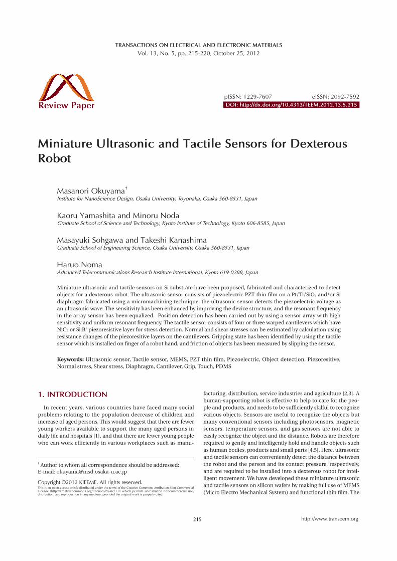
A schematic illustration of an example of the piezoelectric mi-cro-machined ultrasonic sensor (pMUT) is shown together with a plan photograph of center diaphragm in Fig. 1 [16]. The square diaphragm of the SiO2 or SiO2/Si films was fabricated from a pho-tolithograph of the reverse side of a square SiO2 thin film and the preferential etching of a silicon or SOI (Silicon on Insulator) wa-fer underneath the sensitive area [17]. Pt/Ti thin film was formed on the front surface of the diaphragm, the PZT (Pb(Zr,Ti)O3) thin film was successively deposited by the Sol-gel method, and an Au thin film electrode was formed. This structure was placed on a package and the sensor fabrication was completed after wiring. When the ultrasonic wave is applied to the sensor, the diaphragm of the Au/PZT/Pt/Ti/SiO2 and/or SiO2/Si multi-film vibrates up and down at a resonant frequency by air pressure. An ultrasonic array sensor can be easily fabricated by arranging many sensor elements regularly on the Si wafer by using the same fabrication processes.
2.2 Ultrasonic response
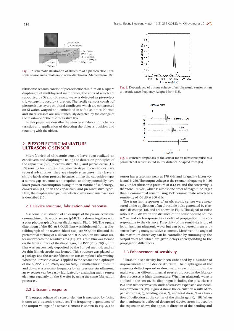
The output voltage of a sensor element is measured by facing it onto an ultrasonic transducer. The frequency dependence of the output voltage of a sensor element is shown in Fig. 2. The
sensor has a resonant peak at 176 kHz and its quality factor (Q-factor) is 250. The output voltage at the resonant frequency is 1.26 meV under ultrasonic pressure of 0.12 Pa and the sensitivity is therefore -39.5 dB, which is almost one order of magnitude larger than a commercial sensor using PZT ceramic plate which has sensitivity of -56 dB at 200 kHz.
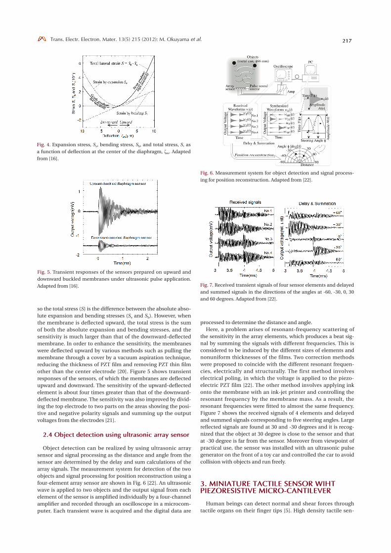
The transient responses of an ultrasonic sensor were mea-sured under application of an ultrasonic pulse generated by elec-trical discharge [18], and are shown in Fig. 3. The signal-to-noise ratio is 23.7 dB when the distance of the sensor-sound source is 2 m, and each response has a delay of propagation time cor-responding to the distance. Directivity of the sensitivity is broad for an incident ultrasonic wave, but can be squeezed in an array sensor having many sensitive elements. Moreover, the angle of the maximum directivity can be controlled by summing up the output voltages which are given delays corresponding to the propagation differences.
2.3 Enhancement of sensitivity
Ultrasonic sensitivity has been enhanced by a number of improvements to the device structure. The diaphragms of the elements deflect upward or downward as each thin film in the multilayer has different internal stresses induced in the fabrica-tion processes at high temperature. When an ultrasonic wave is applied to the sensor, the diaphragm including the piezoelectric PZT thin film receives two kinds of stresses: expansion and bend-ing components [19]. Figure 4 shows the calculation results of ex-pansion stress, Se, bending stress, Sb, and total stress, S, as a func-tion of deflection at the center of the diaphragm, ζm [16]. When the membrane is deflected downward (ζm<0), stress induced by the expansion shows the opposite direction of the bending and
Fig. 1. A schematic illustration of structure of a piezoelectric ultra-sonic sensor and a photograph of the diaphragm. Adapted from [16].
Fig. 2. Dependence of output voltage of an ultrasonic sensor on an ultrasonic wave frequency. Adapted from [15].
Fig. 3. Transient responses of the sensor for an ultrasonic pulse as a parameter of sensor-sound source distance. Adapted from [15].
217Trans. Electr. Electron. Mater. 13(5) 215 (2012): M. Okuyama et al.
so the total stress (S) is the difference between the absolute abso-lute expansion and bending stresses (Se and Sb). However, when the membrane is deflected upward, the total stress is the sum of both the absolute expansion and bending stresses, and the sensitivity is much larger than that of the downward-deflected membrane. In order to enhance the sensitivity, the membranes were deflected upward by various methods such as pulling the membrane through a cover by a vacuum aspiration technique, reducing the thickness of PZT film and removing PZT thin film other than the center electrode [20]. Figure 5 shows transient responses of the sensors, of which the membranes are deflected upward and downward. The sensitivity of the upward-deflected element is about four times greater than that of the downward-deflected membrane. The sensitivity was also improved by divid-ing the top electrode to two parts on the areas showing the posi-tive and negative polarity signals and summing up the output voltages from the electrodes [21].
2.4 Object detection using ultrasonic array sensor
Object detection can be realized by using ultrasonic array sensor and signal processing as the distance and angle from the sensor are determined by the delay and sum calculations of the array signals. The measurement system for detection of the two objects and signal processing for position reconstruction using a four-element array sensor are shown in Fig. 6 [22]. An ultrasonic wave is applied to two objects and the output signal from each element of the sensor is amplified individually by a four-channel amplifier and recorded through an oscilloscope in a microcom-puter. Each transient wave is acquired and the digital data are
processed to determine the distance and angle.Here, a problem arises of resonant-frequency scattering of
the sensitivity in the array elements, which produces a beat sig-nal by summing the signals with different frequencies. This is considered to be induced by the different sizes of elements and nonuniform thicknesses of the films. Two correction methods were proposed to coincide with the different resonant frequen-cies, electrically and structurally. The first method involves electrical poling, in which the voltage is applied to the piezo-electric PZT film [22]. The other method involves applying ink onto the membrane with an ink-jet printer and controlling the resonant frequency by the membrane mass. As a result, the resonant frequencies were fitted to almost the same frequency. Figure 7 shows the received signals of 4 elements and delayed and summed signals corresponding to five steering angles. Large reflected signals are found at 30 and -30 degrees and it is recog-nized that the object at 30 degree is close to the sensor and that at -30 degree is far from the sensor. Moreover from viewpoint of practical use, the sensor was installed with an ultrasonic pulse generator on the front of a toy car and controlled the car to avoid collision with objects and run freely.
3. MINIATURE TACTILE SENSOR WIHTPIEZORESISTIVE MICRO-CANTILEVER
Human beings can detect normal and shear forces through tactile organs on their finger tips [5]. High density tactile sen-
Fig. 5. Transient responses of the sensors prepared on upward and downward buckled membranes under ultrasonic pulse application. Adapted from [16].
Fig. 4. Expansion stress, Se, bending stress, Sb, and total stress, S, as a function of deflection at the center of the diaphragm, ζm. Adapted from [16].
Fig. 6. Measurement system for object detection and signal process-ing for position reconstruction. Adapted from [22].
Fig. 7. Received transient signals of four sensor elements and delayed and summed signals in the directions of the angles at -60, -30, 0, 30 and 60 degrees. Adapted from [22].

Trans. Electr. Electron. Mater. 13(5) 215 (2012): M. Okuyama et al.218
sors are required with the ability to detect various forces and soft surfaces such as the human hand. While many types of tactile sensors have previously been proposed [4,5,23-29], high-density tactile sensor arrays that can simultaneously detect normal and shear forces using one sensor element have not yet been real-ized. In this study, we have proposed a tactile sensor with micro-cantilevers embedded in the elastomer (polydimethylsiloxane; PDMS) for dexterous robots and fabricated by MEMS technolo-gies. It is demonstrated that the fabricated tactile sensors can de-tect normal and shear forces simultaneously [30-34]. In the fol-lowing section, the tactile sensors with sensitive cantilevers are described, and a fabricated tactile sensor array was applied for slippage detection when the object is held in the robot’s hands and is slipped.
3.1 Device structure and fabrication
A schematic illustration of an example of a tactile sensor hav-ing four cantilevers sensitive to normal and shear stresses is shown in Fig. 8(a). Each cantilever is warped back by using the difference between internal stresses induced by different ther-mal expansions of multi-layers. One pair of aligned cantilevers is positioned so the cantilevers face each other and the other pair of cantilevers is arranged orthogonally. The cantilevers consist of Si, Si3N4, SiO2, NiCr (or Si:B+) and Cr thin films as shown in Fig. 8(b), and are embedded in a soft and thick PDMS elastomer layer which can be touched and is human-friendly. The NiCr thin film or Si:B+ layer is piezoresistive and sensitive to deformation in-duced by stresses.
The operation principle is shown in Fig. 9. When normal stress is applied to a pair of face-to-face cantilevers as shown in Fig. 9(a), both the cantilevers deflect in the same bending downward direction, and the piezoresistive outputs have the same sign. On the other hand, when shear stress is applied to a pair of face-to-face cantilevers as shown in Fig. 9(b), both the cantilevers deflect in the opposite bending direction and the piezoresistive outputs have opposite signs. Therefore, the normal and shear stresses can be distinguished by calculating the summation and differ-ence of piezoelectric outputs of the face-to-face cantilevers, respectively. Two pairs of orthogonal face-to-face cantilevers provides strength and direction of shear stress added onto the lateral plane and strength of vertical stress simultaneously, and so can detect the tri-axial (x, y and z) force. Moreover, tactile sensors were fabricated having three cantilevers of which the directions were rotated every 120 degrees centrosymmetrically. Three-axis stresses can be estimated from the resistance changes of NiCr films or Si:B+ layers on the three cantilevers as tri-axial stresses can be principally calculated from three variables (re-sistance changes) by solving linear simultaneous equations with three unknowns.
The cantilevers were fabricated on a SOI (silicon on insulator) by micromachining, and were warped from the residual stress in
the Cr thin film, after release from the Si substrate. Piezoresitive NiCr film or Si:B+ layer on the cantilever is combined with three Ni/Cr films or Si:B+ layers to construct a bridge circuit for detec-tion of tiny change of resistance. Although temperature drift or noise is a serious problem in detection by touching a warm ob-ject such as a human body, it is significantly reduced by optimiz-ing the Ni/Cr atomic ratio (Ni/Cr:42/58) [35]. These cantilevers were embedded in PDMS, which were solidified by heating.
3.2 Detection of normal and shear stresses
The response of the tactile sensor fabricated using Si:B+ piez-soresitive layer was measured under normal and shear stresses. The relative changes of resistances of the face-to-face cantile-vers in the sensor for normal stress, ΔR/R are shown in Fig. 10. Normal stress is added in the measurement system shown in the inset and monitored by a 6-axis force sensor (UFS 2A-05 Nitta Corp.) attaching a press rod. The outputs of the left and right cantilevers are proportional to the applied normal stress, and
Fig. 8. (a) Bird’s eye view of structures of tactile sensor having four cantilevers sensitive to normal and shear stresses and (b) cross-section of the cantilever. Adapted from [31].
Fig. 9. Detection principle for sensing (a) normal stress and (b) shear stress. Adapted from [31].
Fig. 10. Relative changes of resistances of Si:B+ piezoresistive layers on face-to-face cantilevers as a function of normal stress. Inset shows measurement system for applying normal stress to the sensor.
Fig. 11. Relative changes of resistances of Si:B+ piezoresistive lay-ers on cantilevers faced in the force direction as a function of shear stress. Inset shows measurement system for applying shear stress to the sensor. Adapted from [32].
(a) (a) (b)(b)

219Trans. Electr. Electron. Mater. 13(5) 215 (2012): M. Okuyama et al.
their difference induced by the difference in the size and thick-ness of the pizpresitive layer, is not large. The response under shear stress was also measured by using the same system, and by adding shear force under small normal force. The relative changes of resistances of left and right cantilevers under shear stress, ΔR/R are shown in Fig. 11. They have opposite sign and their absolute values are close each other. It is confirmed from these results that normal and shear stresses can be obtained si-multaneously.
3.3 Gripping judgment and friction measurement
3.3.1 Judgment of gripping status by tactile sensor
As a practical application of the tactile sensor, the classifica-tion method of gripping state for the robot hand installed with the sensor array was carried out based on machine learning as shown in Fig. 12 [36,37]. A two-finger type of robot hand with two degrees of freedom was used and a tactile sensor with three cantilevers was placed at an inner side of the finger. Output signals from the sensors are captured by a multi-channel data logger (Keyence corp. NR2000). The object used for the gripping test is an acrylic target box (300 × 50 × 55 mm, 300 g), and a video camera was placed inside the box to observe the contact surface between the object and the sensor through a mirror and classify the gripping states optically.
The experimental sequence was performed as follows. First, the fingers do not touch the target in “non-contact state”. Next, the fingers press the box in “grip (pressed) state”. Then, the fin-gers hold the target stably in “grip (holding) state” where full con-tact between the sensor surface and target is observed. The force applied to the finger is gradually relaxed. When the force is less
than a certain threshold, the finger starts slipping on the object in “grip-slip limit state”. Finally, the object slips in “slip state” and falls down. Under “unstable grip state”, the image of the video camera shows that partial contact occurs in the contact surface. The gripping state was identified by comparing the absolute sen-sor output, the slope of the output transient, and the dispersion during the previous 0.5 sec. Table 1 shows the classification of gripping states estimated by using the output of the tactile sen-sor. Three stable states of “non-contact”, “grip (holding)” and “slip” can be estimated with high probability from the output data of the tactile sensor, but the intermediate states of the “grip (pressed)” and “grip-slip limit” are difficult to estimate as the probabilities are low.
3.3.2 Friction measurement by moving tactile sensor on object
A tactile sensor array covered by a projected cylindrical elas-tomer has been designed and fabricated for crosstalk reduction between sensor elements caused by the lateral deformation of the elastomer. The analysis of elastomer deformation by the fi-nite element method showed that the optimal thickness of the flat elastomer on the substrate except for the cylinders is 50-100 μm, because the sensor structure has not only a low crosstalk but also considerable robustness [34]. A tactile sensor array hav-ing the flat elastomer of 70 μm thickness has little crosstalk and high robustness. Friction between the tactile sensor and some object was measured by slipping the sensor onto objects. Figure 13 shows transient change of relative resistance, ΔR/R when the sensor is slipped on Si and polystyrene plates at constant speed under normal force of 65 gf. The sensor moves laterally from about 3.2 sec and ΔR/R abruptly jumps up. The maximum ΔR/R is dependent on coefficient of static friction and roughness of the object surface and so the sense of touch can be characterized by this measurement. ΔR/R becomes reduced and/or oscillated from the maximum point. The reduction of ΔR/R is considered to be due to smaller coefficient of kinetic friction than coefficient of static friction and the oscillation may be due to stick-slip phe-nomena.
4. CONCLUSION
Miniature ultrasonic and tactile sensors have been proposed, fabricated and characterized for a dexterous robot. The ultra-sonic sensor consists of a sol-gel PZT piezoelectric film on a diaphragm fabricated on Si and vibration induced by ultrasonic pressure produces an electrical signal through piezoelectric ef-fect. Sensitivity of the sensor has been enhanced by buckling
Fig. 12. Schematic illustration of measurement system for detecting slippage. Tactile sensors are installed on the finger surface of the ro-bot’s hand which grips a box. A video camera in the box records grip-ping states. Adapted from [36].
Table 1. Classification of five gripping states estimated from output of tactile sensor.
Non-
contact
Grip
(pressed)
Grip
(holding)
Grip-Slip
limitSlip
Identification
probabilityNon-
contact1,705 0 0 0 5 99.7%
Grip
(pressed)59 143 206 23 130 25.5%
Grip
(holding)0 0 6,922 422 0 94.3%
Grip-Slip
limit0 338 70 151 632 12.7%
Slip 0 0 0 0 400 100.0%
Fig. 13. Relative resistance changes of tactile sensor slipping on Si and polystyrene surfaces. Inset shows cross-section of used tactile sensor array.
Trans. Electr. Electron. Mater. 13(5) 215 (2012): M. Okuyama et al.220
the diaphragm upward and summing outputs of top electrodes divided to two parts. The distance between the sensor and object was easily estimated from the time delay of the wave propaga-tion. Moreover, the stereographic position of objects can be estimated by the processing of signals obtained from the sensor array elements whose resonant frequencies of sensitivity are co-incided. The miniature tactile sensor consists of a NiCr thin film or Si:B+ layer on warped cantilevers on Si, which is embedded in soft PDMS elastomer. Face-to-face cantilevers have the same and opposite stresses under normal pressure and shear stresses, respectively, and are distinguished by the summation and dif-ference of resistance change of piesoresistive layer. Moreover, gripping states are found to be identified by signal processing of normal stress and shear stress outputs. The sense of touch can be identified quantitatively by slipping the tactile sensor onto objects. These two ultrasonic and tactile sensors are expected to be very useful for assisting action of a dexterous robot.
REFERENCES
[1] M. Onishi, Z. ~Luo, T. Odashima, S. Hirano, K. Tahara, T. Mukai, 2007 IEEE Int. Conf. on Robotics and Automation, Roma, Italy, April 10-14, 3128 (2007).
[2] M. Fujii, W. Inamura, H. Murakami, K. Tanaka, K. Kosuge, Proc. 2007 IEEE. Int. Conf. Robotics Biomimetics (2007) p.816 [DOI : http://dx.doi.org/10.1109/ROBIO.2007.4522268].
[3] K. Noda, Y. Hashimoto, Y. Tanaka, I. Shimoyama, Transducers 2009, Denver CO, USA (2009) p.2176.
[4] M. H. Lee, H. R. Nicholls, Mechatronics 9, 1 (1999) [DOI : http://dx.doi.org/ 10.1016/S0957-4158(98)00045-2].
[5] R. S. Dahiya, G. Metta, M. Valle, G. Sandini, IEEE Trans. Robotics 26, 1(2010) [DOI : http://dx.doi.org/10.1109/TRO.2009.2033627].
[6] B. T. Khuri-Yakub, C.H. Cheng, F.L. Degertekin, S. Ergun, S. Hansen, X.C. Jin, O. Oralkan, Jpn. J. Appl. Phys. 39, 2883 (2000) [DOI: http://dx.doi.org/10.1143/JJAP.39.2883].
[7] S. Aoyagi, K. Furukawa, K. Yamashita, T. Tanaka, K. Inoue, M. Okuyama, Jpn. J. Appl. Phys. 46, 4595 (2007) [DOI: http://dx.doi.org/10.1143/JJAP.46.4595].
[8] X. Jin, I. Ladabaum, B. T. Khuri-Yakub, IEEE J. Micro-electromech. Syst. 7, 295 (1998) [DOI : http://dx.doi.org/10.1109/84.709646] .
[9] J. J. Neumann, D.W. Greve, I. J. Oppenheim, Comparison of piezoresistive and capacitive ultrasonic transducers, in: SPIE Smart Structure Conference 2004, San Diego, USA, March 14-18, 2004, pp. 230-238.
[10] Y. Hashimoto, A. Nakai, H. Kawano, K. Matsumoto, I. Shi-moyama, in: Asia Pacific Conference of Transducers and Micro-NanoTechnologies 2008, Vol. 2, Tainan, Taiwan, June 22-25, 2008, pp. 2-3.
[11] K. Ohtani, M. Okuyama, Y. Hamakawa, PbTiO3 thin film ultra-sonic microsensor fabricated on Si wafer, Jpn. J. Appl. Phys. Suppl. 23, 13 (1984).
[12] J. T. Bernstein, S. L. Finberg, K. Houston, L. C. Niles, H. D. Chen, L. E. Corss, K. K. Lee, K. Udayakumar, IEEE Trans. Ul-trason. Ferro. Freq. Cont. 44, 960 (1997) [DOI : http://dx.doi.org/10.1109/58.655620].
[13] P. Muralt, D. Schmitt, N. Ledermann, J. Baborowski, P. K. Weber, W. Steichen, S. Petitgrand, A. Bosseboeuf, N. Setter, P. Gaucher, IEEE Ultrason. Symp. Proc., New York , October 7-10 (2001) p. 907. [DOI : http://dx.doi.org/10.1109/ULTSYM.2001.991867].
[14] Z. H. Wang, J.M. Miao, T. Xu, G. Barbastathis, M. Triantaffylou, Tech. Dig. Transducers 2009, Denver, USA, June 21-25, 2009, p. 1553-1556.
[15] K. Yamashita, H. Katata, M. Okuyama, H. Miyoshi, G. Kato, S.
Aoyagi, Y. Suzuki, Sens. Actuators A 97-98, 302 (2002) [DOI : http://dx.doi.org/10.1016/S0924-4247 (02) 00037-7].
[16] K. Yamashita, T. Yoshizaki, M. Noda, M. Okuyama, IEEJ Trans. on Sensors and Micromachines 131, 235(2011) [DOI: http://dx.doi.org/10.3938/jkps.55.902]
[17] K. Yamashita, T. Yoshizaki, M. Noda, M. Okuyama, J. Korean Phys. Soc. 55, 902 (2009). [DOI: http://dx.doi.org/10.3938/jkps.55.902].
[18] S. Aoyagi, Y. Kamiya, S. Okabe, Jpn. J. Appl. Phys. 31-1 (Suppl.), 263 (1991).
[19] K. Yamashita, H. Nishimoto, M. Okuyama, Sens. Actuators A 139, 118 (2007).
[20] K. Yamashita, T. Watanabe, T. Yoshizaki, M. Noda, M. Okuyama, Sensors and Actuators A 165, 54 (2011)[ DOI:10.1016/j.sna.2010.04.007].
[21] K. Yamashita, M. Okuyama, Sens. Actuators A 127 (2006) 119-122 [DOI : http://dx.doi.org/10.1016/j.sna.2005.11.001].
[22] K. Yamashita, L. Chansomphou, H. Murakami and M. Okuyama, Sensors and Actuators A 114, 147 (2004) [ DOI: http://dx.doi.org/10.1016/j.sna.2003.11.015].
[23] Z. Chu, P. M. Sarro, S. Middelhoek, Sens. Actuators A 54, 505 (1996) [DOI : http://dx.doi.org/10.1016/S0924-4247(95)01190-0].
[24] K. Noda, K. Hoshino, K. Matsumoto, and I. .Shimoyama, Sens. Actuators A 127, 295 (2006) [DOI : http://dx.doi.org/10.1016/j.sna.2005.09.023].
[25] D. J. Heever, K. Schreve, C. Scheer, IEEE Sens. J. 9, 29(2009) [DOI : 10.1109/JSEN.2008.2008891].
[26] C.-S. Park, J. Park, D. -W. Lee, Microeletron. Eng. 86, 1250(2009) [DOI : http://dx.doi.org/10.1016/j.mee.2008.12.072].
[27] Y.-C. Liu, C.-M. Sun, L.-Y. Lin, M.-H. Tsai, and W. Fang, Trans-ducers 2009, Denver CO, USA (2009) p.2190.
[28] M. Shimojo, T. Araki, A. Ming, M. Ishikawa, IEEE Sens. J. 10, 822 (2010) [DOI : 10.1109/JSEN.2009.2034982].
[29] C.-S. Kim, B. K. Kang, J. H. Jung, M. J. Lee, H. B. Kim, S. S. Oh, S. H. Jang, H. J. Lee, H. Kastuyoshi, J. K. Shin, Jpn. J. Appl. Phys. 49, 03CC03 (2010) [DOI : http://dx.doi.org/10.1143/JJAP.49.03CC03].
[30] M. Sohgawa, Y. M. Huang, T. Kanashima, K. Yamashita, M. Noda, M. Okuyama, H. Noma, Transducers'07, Lyon, France (2007) p.1461.
[31] M. Sohgawa, Y. -M. Huang, M. Noda, T. Kanashima, K. Yamashi-ta, M. Okuyama, M. Ikeda, H. Noma, Mater. Res. Soc. Symp. Proc.1052 (2008) p.151 [DOI: http://dx.doi.org/10.1557/PROC-1052-DD04-07].
[32] M. Sohgawa, H. Onishi, T. Mima, Y. -M. Huang, T. Kanashima, K. Yamashita, M. Noda, M. Okuyama, M. Ikeda, H. Noma, Asia-Pacific Conf. on Transducers and Micro-Nano Tech., Tainan, Taiwan (2008).
[33] M. Sohgawa, T. Mima, H. Onishi, T. Kanashima, M. Okuyama, K. Yamashita, M. Noda, M. Higuchi, H. Noma, Transducers 2009, Denver CO, USA (2009) p.284.
[34] M. Sohgawa, T. Uematsu, W. Mito, T. Kanashima, M. Okuyama, H. Noma, Jpn. J. Appl. Phys. 50, 06GM08 (2011) [DOI: http://dx.doi.org/10.1143/JJAP.50.06GM08].
[35] H. Onishi, M. Sohgawa, H. Tachibana, Y. M. Huang, T. Kanashi-ma, M. Okuyama, K. Yamashita, M. Noda, H. Noma, IEEJ Trans. on Sensors and Micromachines 129, 411(2009) [DOI : http://dx.doi.org/10.1541/ieejsmas.129.411].
[36] M. Sohgawa, D. Hirashimaa, Y. Moriguchia, T. Uematsua, W. Mito, T. Kanashima, M. Okuyama and H. Noma, to be pub-lished in Sensors and Actuators A.
[37] W. Mito, H. Yamazoe, S. Yoshida,.M. Tada, M. Sohgawa, T. Kanashima, M. Okuyama, and H. Noma, The 8th France-Japan and 6th Europe-Asia Congress on Mechanics, Yokohama, Japan, 2010 Nov 22-24) p. 260.


![PZT 압전재료.ppt [호환 모드]](https://static.fdocuments.in/doc/165x107/61b3808861533b67b44eb4fc/pzt-ppt-.jpg)


