Mini or Micro-USB Interface IC 34827 - nxp.com · Type 1 cable is attached. After identifying the...
59
Document Number: MC34827 Rev. 3.0, 6/2014 Freescale Semiconductor Technical Data © Freescale Semiconductor, Inc., 2011 - 2014. All rights reserved. Mini or Micro-USB Interface IC The 34827 is a dedicated IC for managing charging and signal multiplexing between a cell phone and its accessory via a 5-pin Mini or Micro-USB connector. An external power source, such as a dedicated AC/DC adapter or a standard USB port, is able to charge the battery in the cell phone via the connector. The 34827 is capable of identifying the type of the external power source and selecting one of two battery charge current levels according to the type. The internal power switch can protect the phone system against 28 V power supply input. The 34827 is also able to multiplex the 5 pins to support UART and High- Speed USB 2.0 data communication, mono/stereo-audio/microphone headset with or without a cord remote control, manufacturing or R/D test cables and other accessories. To identify what accessory is plugged into the Mini or Micro-USB connector, the 34827 supports various detection mechanisms, including the VBUS detection and ID detection. A high accurate 5-bit ADC is offered to distinguish the 32 levels of ID resistance and to identify the button pressed in a cord remote control while an Audio Type 1 cable is attached. After identifying the accessory attached, the 34827 configures itself to support the accessory and interrupts a host via an I 2 C serial bus for further actions. The 34827 is also able to identify some non-supported accessory, such as video cable, Phone- Powered Devices and USB OTG devices. The host controls the 34827 via the I 2 C serial bus. This device is powered using SMARTMOS technology. Features • Automatically identifies the power supply type and sets one of two battery-charge-current levels • Internal power switch protects the phone system against 28 V power supply input • Supports stereo/mono headset with or without micro phone and remote control • Supports USB or UART test and R/D cables • High speed USB2.0 compliant • Supports 32 ID resistance values with a high-accuracy 5-bit ADC • I 2 C interface with interrupt to the host • 10 μA quiescent current in Standby mode Figure 1. MC34827 Simplified Application Diagram INTERFACE IC (PB-FREE) 98ASA00050D 20-PIN UTQFN-EP 34827 (PB-FREE) 98ASA00037D 20-PIN UTQFN-EP Applications • Cell phones • MP3/MP4 players • Portable voice recorders • USB universal charging solution (UCS-OMTP) • Supports mini/micro - USB connector • UART and USB high speed communication • Remote control/accessories IDs VDDIO I2C_SCL BASEBAND 34827 I2C_SDA INTB RXD D- TXD D+ BOOT SPK_L ID DP DM JIG SPK_R MIC ISET OUT VBUS VDD GND Charger V BUS ID D+ D- GND USB CONNECTOR Li+ GPIO I 2 C UART USB XCVR Test Port Audio
Transcript of Mini or Micro-USB Interface IC 34827 - nxp.com · Type 1 cable is attached. After identifying the...

Document Number: MC34827Rev. 3.0, 6/2014
Freescale Semiconductor Technical Data
Mini or Micro-USB Interface ICThe 34827 is a dedicated IC for managing charging and signal multiplexing between a cell phone and its accessory via a 5-pin Mini or Micro-USB connector. An external power source, such as a dedicated AC/DC adapter or a standard USB port, is able to charge the battery in the cell phone via the connector. The 34827 is capable of identifying the type of the external power source and selecting one of two battery charge current levels according to the type. The internal power switch can protect the phone system against 28 V power supply input. The 34827 is also able to multiplex the 5 pins to support UART and High-Speed USB 2.0 data communication, mono/stereo-audio/microphone headset with or without a cord remote control, manufacturing or R/D test cables and other accessories.To identify what accessory is plugged into the Mini or Micro-USB connector, the 34827 supports various detection mechanisms, including the VBUS detection and ID detection. A high accurate 5-bit ADC is offered to distinguish the 32 levels of ID resistance and to identify the button pressed in a cord remote control while an Audio Type 1 cable is attached. After identifying the accessory attached, the 34827 configures itself to support the accessory and interrupts a host via an I2C serial bus for further actions. The 34827 is also able to identify some non-supported accessory, such as video cable, Phone-Powered Devices and USB OTG devices. The host controls the 34827 via the I2C serial bus. This device is powered using SMARTMOS technology.Features• Automatically identifies the power supply type and sets one of two
battery-charge-current levels• Internal power switch protects the phone system against 28 V power
supply input• Supports stereo/mono headset with or without micro phone and
remote control• Supports USB or UART test and R/D cables• High speed USB2.0 compliant• Supports 32 ID resistance values with a high-accuracy 5-bit ADC• I2C interface with interrupt to the host• 10 μA quiescent current in Standby mode
Figure 1. MC34827 Simplified Application Diagram
INTERFACE IC
(PB-FREE)98ASA00050D
20-PIN UTQFN-EP
34827
(PB-FREE)98ASA00037D
20-PIN UTQFN-EP
Applications• Cell phones• MP3/MP4 players• Portable voice recorders• USB universal charging solution (UCS-OMTP)• Supports mini/micro - USB connector• UART and USB high speed communication• Remote control/accessories IDs
VDDIO
I2C_SCL
BASEBAND
34827
I2C_SDA
INTB
RXD
D-
TXD
D+
BOOTSPK_L ID
DPDM
JIG
SPK_RMIC
ISET
OUTVBUS
VDD
GND
Charger
VBUS
IDD+D-GND
USB CONNECTOR
Li+GPIO
I2C
UART
USB XCVR
Test Port
Audio
© Freescale Semiconductor, Inc., 2011 - 2014. All rights reserved.
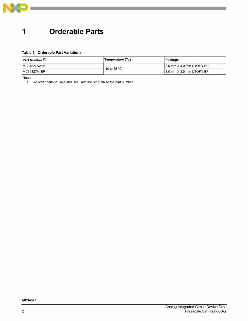
1 Orderable Parts
Table 1. Orderable Part Variations
Part Number (1) Temperature (TA) Package
MC34827A2EP-40 to 85 °C
3.0 mm X 4.0 mm UTQFN-EP
MC34827A1EP 3.0 mm X 3.0 mm UTQFN-EP
Notes1. To order parts in Tape and Reel, add the R2 suffix to the part number.
Analog Integrated Circuit Device Data 2 Freescale Semiconductor
MC34827

INTERNAL BLOCK DIAGRAM
INTERNAL BLOCK DIAGRAM
Figure 2. MC34827 Simplified Internal Block Diagram
VDDIO
I2C_SDA
I2C_SCL
INTB
JIGBOOT
RxD
TxD
D+
D-
SPK_R
SPK_LMIC
VDD
VBUS
OUT
ISET
DP
DM
ID
GND
Reset
I2CInterface
Interrupt
JIGLogic
Output
UARTSwitches
USBSwitches
AudioSwitches
OSC
VBUSDetect
Registerand
StateMachine
VBUS
InternalSupplies
GateDrive and
OCP
ID ADC
IDDetect
Analog Integrated Circuit Device Data Freescale Semiconductor 3
MC34827

PIN CONNECTIONS
PIN CONNECTIONS
Figure 3. MC34827 Pin Connections Table 2. MC34827 Pin Definitions
A functional description of each pin can be found in the Functional Pin Description section beginning on page 14.
Pin Number Pin Name Pin Function Formal Name Definition
1 SPK_R Input Speaker right channel Right channel input of the speaker signals
2 SPK_L Input Speaker left channel Left channel input of the speaker signals
3 MIC Output Microphone output Microphone output to the baseband of the cell phone system
4 D+ IO D+ of the USB transceiver
D+ line of the USB transceiver
5 D- IO D- of the USB transceiver
D- line of the USB transceiver
6 RxD Output UART receiver Receive line of the UART
7 TxD Input UART transmitter Transmit line of the UART
8 BOOT Output BOOT indicator Push-pull output to indicate the boot switch setting of the jig cable
9 VDDIO Input IO power supply IO supply voltage. This is the internal supply voltage for the BOOT and INTB outputs. It can supply the external pull-up voltages for the JIG pin and the I2C bus outside the 34827. This pin also functions as the hardware reset to the IC.
10 JIG Output JIG indicator Open-drain output to indicate the insertion of a jig cable
11 VDD Input Power supply Supply input
12 INTB Output Interrupt output Push-pull interrupt output
13 I2C_SDA IO I2C Data Data line of the I2C interface
14 I2C_SCL Input I2C Clock Clock line of the I2C interface
15 OUT Output Power output The output of the power MOSFET pass switch
16 ISET Output Charge current setting Open-drain output to set the charger current
17 VBUS Input VBUS power supply Mini-USB VBUS line
2
3
4
5
6
15
14
13
12
11
17181920
10987
SPK_L
MIC
D+
D- INTB
I2C_SDA
I2C_SCLOUT
VDD
SPK_RD
PD
M
VBU
S
ISET
JIG
RxD
TxD
VDD
IO
BO
OT
GND
1 16
ID
21
1
2
3
4
5
15
14
13
12
11
1617181920
109876D+
SPK_L
D-
GND
SPK_R
MIC
INTB
I2C_SDA
I2C_SCL
OUT
VDD
DP
DM
VBU
S
ISET
JIG
RxD
TxD
VDD
IO
BO
OT
ID
21
(A). Pinout of 34827 Using a 3.0 mm X 4.0 mm 20 Pin. UTQFN Package(Transparent Top View)
(B). Pinout of 34827 Using a 3.0 mm X 3.0 mm 20 Pin. UTQFN Package(Transparent Top View)
Analog Integrated Circuit Device Data 4 Freescale Semiconductor
MC34827

PIN CONNECTIONS
18 DM IO D- of the USB connector
D- line of the mini-USB connector
19 DP IO D+ of the USB connector
D+ line of the mini-USB connector
20 ID Input ID of the USB connector
ID pin of the mini-USB connector
21 GND Ground Ground Ground
Table 2. MC34827 Pin Definitions (continued)A functional description of each pin can be found in the Functional Pin Description section beginning on page 14.
Pin Number Pin Name Pin Function Formal Name Definition
Analog Integrated Circuit Device Data Freescale Semiconductor 5
MC34827
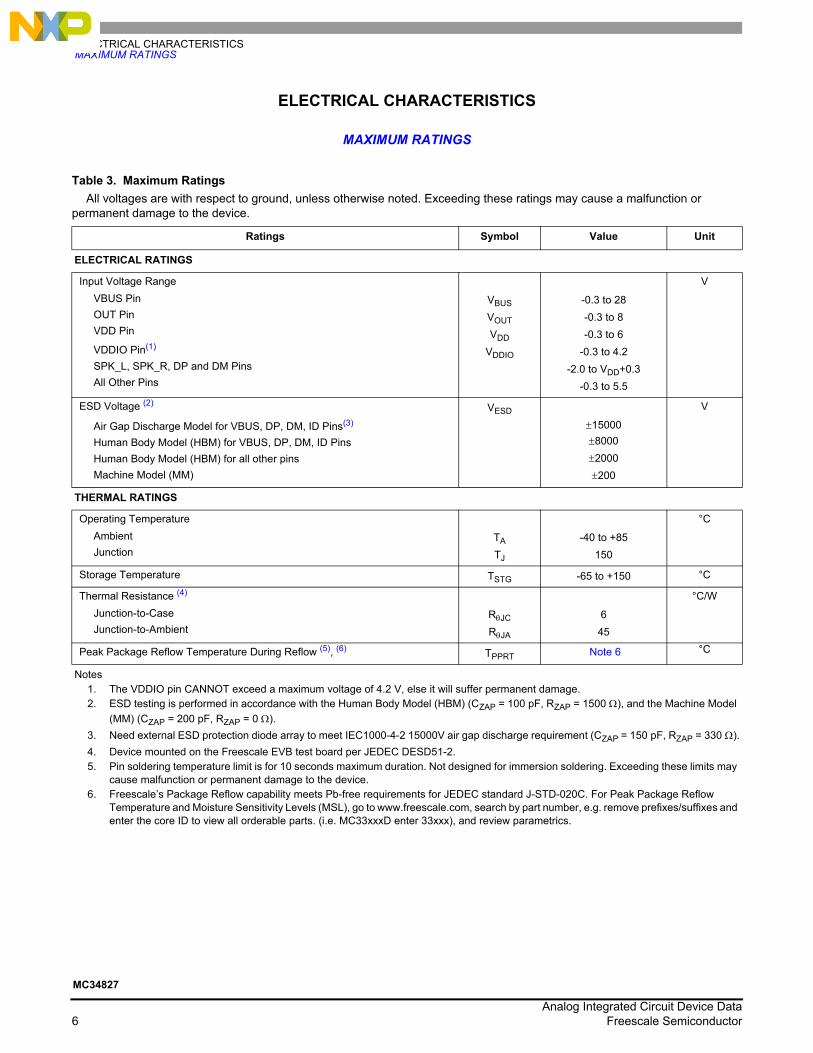
ELECTRICAL CHARACTERISTICSMAXIMUM RATINGS
ELECTRICAL CHARACTERISTICS
MAXIMUM RATINGS
Table 3. Maximum Ratings
All voltages are with respect to ground, unless otherwise noted. Exceeding these ratings may cause a malfunction or permanent damage to the device.
Ratings Symbol Value Unit
ELECTRICAL RATINGS
Input Voltage RangeVBUS PinOUT PinVDD Pin
VDDIO Pin(1)
SPK_L, SPK_R, DP and DM PinsAll Other Pins
VBUS
VOUT
VDD
VDDIO
-0.3 to 28-0.3 to 8-0.3 to 6
-0.3 to 4.2-2.0 to VDD+0.3
-0.3 to 5.5
V
ESD Voltage (2)
Air Gap Discharge Model for VBUS, DP, DM, ID Pins(3)
Human Body Model (HBM) for VBUS, DP, DM, ID PinsHuman Body Model (HBM) for all other pinsMachine Model (MM)
VESD
±15000±8000±2000±200
V
THERMAL RATINGS
Operating TemperatureAmbientJunction
TA
TJ
-40 to +85150
°C
Storage Temperature TSTG -65 to +150 °C
Thermal Resistance (4)
Junction-to-CaseJunction-to-Ambient
RθJC RθJA
645
°C/W
Peak Package Reflow Temperature During Reflow (5), (6) TPPRT Note 6 °C
Notes1. The VDDIO pin CANNOT exceed a maximum voltage of 4.2 V, else it will suffer permanent damage.2. ESD testing is performed in accordance with the Human Body Model (HBM) (CZAP = 100 pF, RZAP = 1500 Ω), and the Machine Model
(MM) (CZAP = 200 pF, RZAP = 0 Ω).3. Need external ESD protection diode array to meet IEC1000-4-2 15000V air gap discharge requirement (CZAP = 150 pF, RZAP = 330 Ω).4. Device mounted on the Freescale EVB test board per JEDEC DESD51-2. 5. Pin soldering temperature limit is for 10 seconds maximum duration. Not designed for immersion soldering. Exceeding these limits may
cause malfunction or permanent damage to the device.6. Freescale’s Package Reflow capability meets Pb-free requirements for JEDEC standard J-STD-020C. For Peak Package Reflow
Temperature and Moisture Sensitivity Levels (MSL), go to www.freescale.com, search by part number, e.g. remove prefixes/suffixes and enter the core ID to view all orderable parts. (i.e. MC33xxxD enter 33xxx), and review parametrics.
Analog Integrated Circuit Device Data 6 Freescale Semiconductor
MC34827

ELECTRICAL CHARACTERISTICSSTATIC ELECTRICAL CHARACTERISTICS
STATIC ELECTRICAL CHARACTERISTICS
Table 4. Static Electrical Characteristics
Characteristics noted under conditions VDD = 3.6 V, VBUS = 5.0 V, VDDIO = 3.0 V, -40 °C ≤ TA ≤ 85 °C (see Figure 1), unless otherwise noted. Typical values noted reflect the approximate parameter means at VDD = 3.6 V and TA = 25 °C under nominal conditions, unless otherwise noted.
Characteristic Symbol Min Typ Max Unit
POWER INPUT
Recommended Operating Voltage Range for VDD Supply Voltage VDD 2.7 - 5.5 V
VDD Power-on Reset ThresholdRising edgeHysteresis
VVDDPOR
--
2.5100
2.65-
VmV
VDD Quiescent CurrentIn Standby modeIn Power Save modeWhen accessory is attached & INT_MASK = ‘1’In Active mode (VDD < VBUS)In Active mode (VDD > VBUS)
IVDD
-----
9.012
125550850
1218
160650
1000
μA
VBUS Supply Voltage VBUS 2.8 5.0 28 V
VBUS Detection Threshold VoltageRising edgeHysteresis
VBUS_DET
--
2.65150
2.80-
VmV
VBUS Supply Quiescent Current In VBUS power mode In Active mode - Dedicated Charger
In Active mode - Audio or TTY(7) (VBUS < VDD)
IVBUS
---
---
1.21.20.5
mAmAμA
VBUS Over-voltage Protection ThresholdRising edgeHysteresis
VBUS_OVP
6.8-
7.0150
7.2-
VmV
VBUS Over-current ProtectionTriggering threshold (at onset of OTP shutoff)
IBUS_OCP
1.2 1.8 2.2 A
Over-temperature Protection ThresholdRising thresholdFalling threshold
TOTP
115-
13095
145-
°C
VDDIO Supply Voltage VDDIO 1.65 - 3.6 V
SWITCH
ISET Open-drain Output MOSFETOn resistance (loaded by 3.0 mA current)Leakage current (when the MOSFET is off at 5.0 V bias voltage)
RISET
IISET_OFF
--
--
1000.5
Ω
μA
OUT Pin Discharge MOSFET(16)
On resistance (loaded by 3.0 mA current)Leakage current (when the MOSFET is off at 5.0 V bias voltage)
ROUT_DISC
IOUT_OFF
--
-0.5
100-
Ω
μA
Notes7. This is an important specification because when an audio accessory is attached, the VBUS line is connected to the microphone. The
quiescent current will affect the bias of the microphone.8. The OUT pin discharge MOSFET is shown in Figure 20. This MOSFET will be turned on when the power MOSFET is off.
Analog Integrated Circuit Device Data Freescale Semiconductor 7
MC34827

ELECTRICAL CHARACTERISTICSSTATIC ELECTRICAL CHARACTERISTICS
Power MOSFET On resistance (when VBUS = 5.0 V, TA< 50 °C)
RPSW
- 200 250mΩ
SPK_L and SPK_R SwitchesOn resistance (20 Hz to 470 kHz)Matching between channelsOn resistance flatness (from -1.2 V to 1.2 V)
RSPK_ON
RSPK_ONMCT
RSPK_ONFLT
---
1.60.120.01
3.00.250.05
Ω
D+ and D- SwitchesOn resistance (0.1 Hz to 240 MHz)Matching between channelsOn resistance flatness (from 0.0 V to 3.3 V)
RUSB_ON
RUSB_ONMCT
RUSB_ONFLT
---
-0.1
0.02
5.00.50.1
Ω
RxD and TxD SwitchesOn resistanceOn resistance flatness (from 0.0 V to 3.3 V)
RUART_ON
RUART_ONFLT
--
--
605.0
Ω
MIC SwitchesOn resistance (at below 2.3 V MIC bias voltage)On resistance flatness (from 1.8 V to 2.3 V)
RMIC_ON
RMIC_ONFLT
--
--
1005.0
Ω
Pull-down Resistors between SPK_L or SPK_R Pins to GND RPD_AUDIO - 100 - kΩ
Signal Voltage RangeSPK_L, SPK_R,D+, D-, RxD, TxD, MIC
-1.5-0.3
--
1.53.6
V
PSRR - From VDD (100 mVrms) to DP/DM Pins (9)
20 Hz to 20 kHz with 32/16 Ω load.VA_PSRR
- - -60dB
Total Harmonic Distortion(9)
20 Hz to 20 kHz with 32/16 Ω load.THD
- - 0.05%
Crosstalk between Two Channels(9)
20 Hz to 20 kHz with 32/16 Ω load.VA_CT
- - -50dΒ
Off-Channel Isolation(9)
Less than 1.0 MHzVA_ISO
- - -100dB
POWER SUPPLY TYPE IDENTIFICATION
Data Source Voltage
Loaded by 0~200 μAVDAT_SRC
0.5 0.6 0.7V
Data Source Current IDAT_SRC 0 - 200 μA
Data Detect Voltage VDAT_REF 0.3 0.35 0.4 V
Car Kit Detect Voltage VCR_REF 0.8 0.9 1.0 V
Data Sink CurrentDM pin is biased between 0.15 to 3.6 V
IDAT_SINK
65 100 135μA
DP, DM Pin Capacitance CDP/DM - 8.0 - pF
Notes9. Not tested. Guaranteed by design.
Table 4. Static Electrical Characteristics (continued)Characteristics noted under conditions VDD = 3.6 V, VBUS = 5.0 V, VDDIO = 3.0 V, -40 °C ≤ TA ≤ 85 °C (see Figure 1), unless
otherwise noted. Typical values noted reflect the approximate parameter means at VDD = 3.6 V and TA = 25 °C under nominal conditions, unless otherwise noted.
Characteristic Symbol Min Typ Max Unit
Analog Integrated Circuit Device Data 8 Freescale Semiconductor
MC34827

ELECTRICAL CHARACTERISTICSSTATIC ELECTRICAL CHARACTERISTICS
DP, DM Pin ImpedanceAll switches are off (Switch_Open = 0)
RDP/DM
- 50 -MΩ
ID DETECTION
ID FLOAT ThresholdDetection threshold
VFLOAT
- 2.3 -V
Pull-up Current SourceWhen ADC Result is 1xxxxWhen ADC Result is 0xxxx
IID1.9
30.42.032
2.133.6
μA
Video Cable Detection Detection currentDetection voltage low thresholdDetection voltage high threshold
IVCBL
VVCBL_L
VVCBL_H
1.0--
1.250
118
1.4--
mAmVmV
LOGIC INPUT AND OUTPUT
VDDIO Logic Input ThresholdInput LOW thresholdInput HIGH threshold
VDDIO_IL
VDDIO_IH
-1.5
--
0.5-
VV
Push-Pull Logic Output (INTB and BOOT)Output HIGH level (loaded by 1.0 mA current)Output LOW level (loaded by 4.0 mA current)
VOH
VOL
0.7VDDIO
---
-0.4
V
Open-Drain Logic Output (JIG)Output LOW level (loaded by 4.0 mA current)
VJIGOL
- - 0.4V
I2C INTERFACE
Low Voltage on I2C_SDA, I2C_SCL Inputs VI2C_IL -0.2 - 0.3VDDIO V
High Voltage on I2C_SDA, I2C_SCL Inputs VI2C_IH 0.7VDDIO - VDDIO V
Low Voltage on I2C_SDA Output VI2C_OL - - 0.4 V
Current Load when I2C_SDA Outputs Low Voltage II2C_OL 0 - 4.0 mA
Leakage Current on I2C_SDA, I2C_SCL Outputs II2C_LEAK -1.0 - 1.0 μA
Input Capacitance of the I2C_SDA, I2C_SCL Pins(10) CI2CIN - - 8.0 pF
Notes10. Not tested. Guaranteed by design.
Table 4. Static Electrical Characteristics (continued)Characteristics noted under conditions VDD = 3.6 V, VBUS = 5.0 V, VDDIO = 3.0 V, -40 °C ≤ TA ≤ 85 °C (see Figure 1), unless
otherwise noted. Typical values noted reflect the approximate parameter means at VDD = 3.6 V and TA = 25 °C under nominal conditions, unless otherwise noted.
Characteristic Symbol Min Typ Max Unit
Analog Integrated Circuit Device Data Freescale Semiconductor 9
MC34827

ELECTRICAL CHARACTERISTICSDYNAMIC ELECTRICAL CHARACTERISTICS
DYNAMIC ELECTRICAL CHARACTERISTICS
Table 5. Dynamic Electrical Characteristics
Characteristics noted under conditions VDD = 3.6 V, VBUS = 5.0 V, VDDIO = 3.0 V, -40 °C ≤ TA ≤ 85 °C (see Figure 1), unless otherwise noted. Typical values noted reflect the approximate parameter means at VDD = 3.6 V and TA = 25 °C under nominal conditions, unless otherwise noted.
Characteristic Symbol Min Typ Max Unit
POWER ON AND OFF DELAY
VDD Power-on Reset ThresholdVDD rising deglitch time VDD falling deglitch time
tD2
tVDDDGT_F
7.01.7
8.52.5
10.23.5
ms
VBUS Detection Threshold Deglitch Time (for Both Rising and Falling Edges) tVBUS_DET 3.5 4.5 5.7 ms
VBUS Over-voltage Protection
Protection delay(11)
Falling-edge deglitch time(12)
tOVPD
tOVPDGT_F
--
-25
2.0-
μs
VBUS Over-temperature Protection
MOSFET turning off speed when OTP occurs(13)
Deglitch timetOTP_TO
tOTP_DGT
--
-15
0.5-
A/μsμs
OSCILLATOR
Oscillation Frequency fOSC 88 100 112 kHz
SWITCHING DELAY
t1 - t0 (td in Figure 17, Default Value is TD = 0100)TD = 0000TD = 0001TD = 0010TD = 0011TD = 0100...TD = 1111
td-----...-
100200300400500...
1600
-----...-
ms
t2 - t1(Figure 17) tSW 20 - - ms
t3 - t2(Figure 17) tSW 20 - - ms
t4 - t1(Figure 17) tSW 100 - - ms
t6 - t3(Figure 17) tSW 100 - - ms
ID DETECTION
ID FLOAT Detection Deglitch Time tID_FLOAT - 20 - ms
Video Cable Detection Time (Video Cable Detection Current Source On Time) tVCBL - 20 - ms
ADC
ADC Conversion Time tCONV - 1.0 - ms
Notes11. The protection delay is defined as the interval between VBUS voltage rising above the OVP rising threshold, and the OUT pin voltage
dropping below the OVP rising threshold voltage for a VBUS ramp rate of >1.0 V/μs.12. The OVP deglitch timer is only for the falling edge threshold.13. Not tested. Guaranteed by design.
Analog Integrated Circuit Device Data 10 Freescale Semiconductor
MC34827
ELECTRICAL CHARACTERISTICSDYNAMIC ELECTRICAL CHARACTERISTICS
REMOTE CONTROL
Key Press Comparator Debounce Time tRMTCON_DG - 20 - ms
RESET TIMING
Device Reset Time tRSTDVC - 10 - μs
VDDIO Logic Input TimingRising-edge deglitch timeFalling-edge deglitch time
tVDDIODGT_R
tVDDIODGT_F
660105
875125
1130150
μs
VDDIO Reset TimingVDDIO reset pulse width tRSTVDDIO 150 - -
μs
I2C Reset Timing
I2C reset pulse widthI2C_SDA/I2C_SCL concurrent low time without causing reset
tRSTI2C
tNRSTI2C
13.5-
--
-8.8
ms
I2C INTERFACE(14)
SCL Clock Frequency fSCL - - 400 kHz
Bus Free Time between a STOP and START Condition tBUF 1.3 - - μs
Hold Time Repeated START Condition tHD:STA 0.6 - - μs
Low Period of SCL Clock tLOW 1.3 - - μs
High Period of SCL Clock tHIGH 0.6 - - μs
Setup Time for a Repeated START condition tSU:STA 0.6 - - μs
Data Hold Time tHD:DAT 0 - - μs
Data Setup Time tSU:DAT 120 - - ns
Rising Time of Both SDA and SCL Signals tR 20+0.1CB - - ns
Falling Time of Both SDA and SCL Signals tF 20+0.1CB - - ns
Setup Time for STOP Condition tSU:STO 0.6 - - μs
Input Deglitch Time (for Both Rising and Falling Edges) tDGT 55 - 300 ns
Notes14. Not tested. Guaranteed by design.
Table 5. Dynamic Electrical Characteristics Characteristics noted under conditions VDD = 3.6 V, VBUS = 5.0 V, VDDIO = 3.0 V, -40 °C ≤ TA ≤ 85 °C (see Figure 1), unless
otherwise noted. Typical values noted reflect the approximate parameter means at VDD = 3.6 V and TA = 25 °C under nominal conditions, unless otherwise noted.
Characteristic Symbol Min Typ Max Unit
Analog Integrated Circuit Device Data Freescale Semiconductor 11
MC34827

ELECTRICAL CHARACTERISTICSELECTRICAL PERFORMANCE CURVES
ELECTRICAL PERFORMANCE CURVES
Figure 4. SPK Switch On-resistance vs Input Voltage
Figure 5. USB Switch On-resistance vs Input Voltage
Figure 6. UART Switch On-resistance vs Input Voltage
Figure 7. MIC Switch On-resistance vs Input Voltage
Figure 8. VDD Supply Current vs Supply Voltage In Standby Mode
Figure 9. VDD Supply Current vs Temperature In Standby Mode
-1.5 -1.0 -0.5 0.0 0.5 1.0 1.5
1.4
1.6
1.8
2.0
2.2Temperature =85°C
Temperature =25°C
Temperature = -40°C
SPK
Sw
itch
On-
Res
ista
nce (Ω
)
Input Voltage (V)
0.0 0.5 1.0 1.5 2.0 2.5 3.0 3.52.0
2.5
3.0
3.5
4.0
4.5
Temperature = 85°C
Temperature = 25°C
Temperature = -40°C
USB
Sw
itch
On-
Res
ista
nce (Ω
)
Input Voltage (V)
0.0 0.5 1.0 1.5 2.0 2.5 3.0 3.520
25
30
35
40
45
Temperature = 85°C
Temperature = 25°C
Temperature = -40°C
UA
RT
Switc
h O
n-R
esis
tanc
e (Ω
)
Input Voltage (V)
1.8 1.9 2.0 2.1 2.2 2.340
50
60
70
80
90Temperature = 85°C
Temperature = 25°C
MIC
Sw
itch
On-
Res
ista
nce (Ω
)
Input Voltage (V)
Temperature = -40°C
2.5 3.0 3.5 4.0 4.5 5.0 5.58.6
8.8
9.0
9.2
9.4
9.6VD
D S
uppl
y C
urre
nt (μ
A)
VDD Voltage (V)
-40 -20 0 20 40 60 80
7
8
9
10
11
VDD
Cur
rent
(μA)
Temperature (°C)
Analog Integrated Circuit Device Data 12 Freescale Semiconductor
MC34827

ELECTRICAL CHARACTERISTICSELECTRICAL PERFORMANCE CURVES
Figure 10. VBUS Supply Current vs Temperature In VBUS Power Mode
Figure 11. OUT Voltage vs VBUS Voltage
-40 -20 0 20 40 60 80760
780
800
820
840
860
880
900
VBU
S Su
pply
Cur
rent
(μA
)
Temperature (°C)0.0 1.5 3.0 4.5 6.0 7.5 9.0
0.0
1.5
3.0
4.5
6.0
7.5
9.0
OU
T Vo
ltage
(V)
VBUS Voltage (V)
Analog Integrated Circuit Device Data Freescale Semiconductor 13
MC34827

FUNCTIONAL DESCRIPTIONINTRODUCTION
FUNCTIONAL DESCRIPTION
INTRODUCTION
The 34827 is used to identify what is attached to the Mini or Micro-USB connector, configure the signal paths between the phone baseband and the 5-pin connector accordingly, and then inform the baseband of the attachment. It also detects the detachment of accessory and then informs the baseband.
To identify what is plugged into the Mini or Micro-USB connector, the 34827 supports various detection mechanisms, including ID detection and VBUS detection. The detection flow is initiated either by the change of VBUS pin voltage or by the change of ID pin voltage. A high accurate 5-bit ADC is offered to distinguish the 32 levels of ID
resistance. Each level of resistance can be assigned to an accessory or a button in a cord remote controller. Some non-supported accessories, such as video cable, Phone-Powered Devices, USB OTG devices and so on, can also be identified. For 34827, the mapping relationship between the ADC values and the types of accessories is fixed and the detailed information is given in section Application Information.
The detachment of accessory is also monitored by both of the ID detector and the VBUS detector.
The host IC can control the 34827 via an I2C serial bus.
FUNCTIONAL PIN DESCRIPTION
SPEAKER RIGHT CHANNEL (SPK_R)Right channel of the baseband speaker output.
SPEAKER LEFT CHANNEL (SPK_L)Left channel of the baseband speaker output.
MICROPHONE OUTPUT (MIC)Microphone output to the baseband.
D+ OF THE USB TRANSCEIVER (D+)D+ line of the USB transceiver.
D- OF THE USB TRANSCEIVER (D-)D- line of the USB transceiver.
UART RECEIVER (RXD)Receiver line of the UART.
UART TRANSMITTER (TXD)Transmitter line of the UART.
BOOT INDICATOR (BOOT)VDDIO referenced push-pull output to indicate the boot
switch setting of jig cables.
IO POWER SUPPLY (VDDIO)Power supply input for the logic IO interface. Generally the
IO power supply voltage should be the same as the IO voltage used in the cell phone system. VDDIO is also one of hardware reset input sources. A falling edge at this pin will reset the 34827.
JIG INDICATOR (JIG)Open-drain output to indicate the insertion of a jig cable.
POWER SUPPLY (VDD)Power supply input. Bypass to ground with a 1.0 μF
capacitor.
INTERRUPT OUTPUT (INTB)Active low and VDDIO referenced push-pull output. When
the 34827 detects a change of external cable status, this pin outputs low voltage to interrupt the baseband. INTB returns to high voltage once all the interrupt bits are read.
DATA LINE OF THE I2C INTERFACE (I2C_SDA)Data line of the I2C interface. I2C_SDA together with
I2C_SCL is one of hardware reset input sources.
CLOCK LINE OF THE I2C INTERFACE(I2C_SCL)Clock line of the I2C interface. I2C_SCL together with
I2C_SDA is one of hardware reset input sources.
POWER OUTPUT (OUT)Output of the power MOSFET in the 34827. This pin is
connected to a charger. Bypass to ground with a 1.0 μF capacitor.
CHARGE CURRENT SETTING (ISET)Open-drain output to set the charge current for a charger
according to the VBUS power supply type.
VBUS POWER SUPPLY (VBUS)Mini-USB VBUS input. Bypass this pin to ground with a
less than 10nF capacitor. When the attached accessory is an audio kit, this pin is the microphone input to the 34827.
D- OF THE USB CONNECTOR (DM)D- line of the mini-USB connector.
Analog Integrated Circuit Device Data 14 Freescale Semiconductor
MC34827

FUNCTIONAL DESCRIPTIONFUNCTIONAL PIN DESCRIPTION
D+ OF THE USB CONNECTOR (DP)D+ line of the mini-USB connector.
ID OF THE USB CONNECTOR (ID)ID pin of the mini-USB connector.
GROUND (GND)Ground.
Analog Integrated Circuit Device Data Freescale Semiconductor 15
MC34827

FUNCTIONAL DESCRIPTIONFUNCTIONAL INTERNAL BLOCK DESCRIPTION
FUNCTIONAL INTERNAL BLOCK DESCRIPTION
Figure 12. MC34827 Functional Internal Block Diagram
LOGIC AND STATE MACHINEInternal state machine executes the detection and
identification flow and turns on or off the signal switches according to the identification result.
I2C INTERFACEI2C interface circuit is an I2C slave device. It receives
commands and data from an I2C master device and transfers them to internal registers of 34827. It also transfers the data from the registers of 34827 to the I2C master device.
TEST INTERFACETest interface connects to a test block of the baseband.
SWITCH ARRAYSwitch array consist of switches for UART, USB and audio
signal channels.
INTERNAL POWER SUPPLYThis block outputs power supply for the internal digital IO
interface and also outputs high power supply for all internal blocks and for the external battery charger. The input power supplies of the block include VBUS, VDD and VDDIO.
VBUS DETECTThis block detects whether the power supply at VBUS pin
is present.
ID ADCAn internal 5-bit ADC measures the resistance at the ID
pin. The result is sent to the Logic and State Machine block to determine what accessory is attached.
ID DETECTThis block generates current sources and other signals to
the ID pin to help the ID ADC block measure the ID resistance.
Switch Array
I2C Interface
VBUS Detect
Test Interface
Internal Power Supply
Logic & State
Machine
ID ADC ID Detect
Analog Integrated Circuit Device Data 16 Freescale Semiconductor
MC34827

FUNCTIONAL DEVICE OPERATIONOPERATIONAL MODES
FUNCTIONAL DEVICE OPERATION
OPERATIONAL MODES
According to the status of the VBUS and VDD power supplies, the 34827 has five operational modes: Power Down mode, VBUS Power mode, Standby mode, Active mode, and
Power Save mode. The mode-transition diagram is given in Figure 13. Details about the mode-transition conditions can be found in Figure 14.
Figure 13. Mode Transition Diagram
POWER DOWN MODEThe Power Down mode is when neither the VDD nor the
VBUS is powered. In this mode, the IC does not respond to any accessory attachment except for a power supply. When an external power supply is plugged, the 34827 enters the VBUS Power mode.
VBUS POWER MODE34827 enters the VBUS Power mode when VBUS is
powered but VDD is not. The 34827 supports regular USB port, dedicated charger, USB charger, 5 wire charger, charger on the A/V cable and any other accessory with powered VBUS voltage. In VBUS Power mode, the internal power MOSFET is turned on to power the charger IC, charging the battery in the phone. ISET pin outputs high impedance to select a lower charge current level for the charger IC.
STANDBY MODEThe Standby mode is when the VDD voltage is higher than
the POR (Power-On Reset) threshold and no accessory is attached. In this mode only ID detection circuit, I2C interface, and internal registers are powered in order to minimize the quiescent current of VDD. The ID detection circuit samples the status of ID line in a period which can be programmed by
the Device Wake Up bits in Timing Set 1 register (refer to Register Map section for more register information).
In Standby mode, all signal switches and the power MOSFET are turned off. The ISET, JIG pins output high impedance and BOOT pin outputs low logic voltage.
If detecting an accessory attachment, the 34827 moves to the Active mode for further accessory identification.
ACTIVE MODEThe Active mode starts when an accessory is plugged with
VDD powered. The 34827 identifies the accessory, configures the signal paths according to the identification result and interrupts the baseband for further actions. Different functions will be enabled according to the identification result. The quiescent current of VDD in Active mode is dependent on the type of attached accessory. The signal switches can also be turned on manually. See more information in section Control Functions.
Mode can be changed from Active to Standby either by accessory detachment or by I2C programming.
POWER SAVE MODEThe Power Save mode is contributing only for the
accessory of Audio Type 1 or TTY. The 34827 enters into
VDD > VPOR
Active
VDD < VPOR
ID detection or VBUS detection
VDD < VPOR
Standby
I2C resets ACTIVE bit or detachment of accessory
Power Down
VBUS Power
VDD > VPOR
VBUS power up
VBUS power down
Power Save
I2C or detection of no activityI2C or
detection of activity
Detachment of accessory
Analog Integrated Circuit Device Data Freescale Semiconductor 17
MC34827

FUNCTIONAL DEVICE OPERATIONPOWER-UP
Power Save mode to minimize the operating current when Audio Type 1 or TTY accessory is attached but not used. For example, when the Audio Type 1 accessory is attached and the cell phone is not in audio playing mode, the baseband can move the 34827 to the Power Save mode via the I2C programming. The 34827 can also automatically switch to Power Save mode when no activity is detected on the SPK_R or SPK_L pins for a period which can be programmed by the Activity Idle Detection Time bits in Timing Set 1 register. The power consumption in Power Save mode approximates that in Standby mode.
The 34827 can quit the Power Save mode to Active mode by I2C programming or automatically when detecting signal activity. The configuration of the 34827 before switching to the Power Save mode is resumed. The mode can also be changed from Power Save mode directly to Standby mode due to the accessory detachment.
DEVICE MODE REGISTERThe PSAVE bit, ACTIVE bit and RST bit in Device Mode
register hold the information of the device operational mode. The RST bit, which is of R/C type, indicates whether a reset has occurred. The RST is set when a Power-on Reset of
VDD, or a hardware reset of VDDIO input, or a hardware reset of I2C inputs occurs, and it will be cleared when it is read by I2C. The ACTIVE bit and the PSAVE bit together indicate the device mode according to the relationship shown in Table 6. When the device is in VBUS Power mode, registers are not powered up.
The ACTIVE bit and PSAVE bit are of R/W type. The baseband can move the device mode to Standby mode manually by writing 0x00 to the Device Mode register via I2C. If an accessory is still attached during the operation, the accessory identification flow shown in Figure 14 can be re-started.
POWER-UP
The 34827 has four possible power-up scenarios depending on which of the VDD and the VBUS is powered first. The four scenarios correspond to the following four mode transitions (refer to Figure 14):
1. From Power Down to VBUS Power: VBUS is powered up when VVDD < VVDDPOR (VDD POR threshold)
2. From VBUS Power to Standby: VBUS is already powered when the VDD rises above its POR threshold
3. From Power Down to Standby: VDD is powered up when VVBUS < VVBUSPOR (VBUS POR threshold)
4. From Standby to Active: VDD is already powered when VBUS rises above its POR threshold
SCENARIO 1: VDD = 0 V AND VBUS IS POWERED UP (POWER DOWN MODE TO VBUS POWER MODE TRANSITION)
If VDD is not powered but the VBUS is powered up to a voltage range between the POR threshold and the OVP threshold, the internal charge pump for the power MOSFET gate driver starts to operate, softly turning on the power MOSFET. The IC is in the VBUS Power mode.
In this case, the ISET outputs high-impedance, all registers are in reset states.
SCENARIO 2: VBUS = HIGH AND VDD IS POWERED UP (VBUS POWER MODE TO STANDBY MODE TRANSITION)
If the VBUS is already powered up, when VDD is powered, the device moves from the VBUS Power mode to the Standby mode and then quickly move to the VBUS detection flow of the Active mode to identify the accessory, as shown in Figure 14.
After VDD is powered up, the 34827 starts up the internal supplies. The POR resets all register bits. The power MOSFET remains on during the reset process.
SCENARIO 3: VBUS = 0 V AND VDD IS POWERED UP (POWER DOWN MODE TO STANDBY MODE TRANSITION)
If no accessory is plugged, when VDD is powered, the 34827 moves from the Power Down mode to the Standby mode. The internal supplies are started up first, and then the whole chip is reset and is ready to accept accessories. When an accessory is attached, the 34827 enters the Active mode. The power MOSFET is off in this case since VBUS = 0 V.
SCENARIO 4: VDD = HIGH AND VBUS IS POWERED UP (STANDBY TO ACTIVE MODE TRANSITION)
This is a normal VBUS detection case.
Table 6. The Device Modes vs. the Register Bits
PSAVE ACTIVE MODE
0 0 Standby
0 1 Active
1 1 Power Save
1 0 Undefined
Analog Integrated Circuit Device Data 18 Freescale Semiconductor
MC34827

FUNCTIONAL DEVICE OPERATIONACCESSORY IDENTIFICATION
ACCESSORY IDENTIFICATION
The identification flow chart is shown in Figure 14. When an accessory with powered VBUS is attached in
Power Down mode, the 34827 enters VBUS Power mode. The 34827 will not identify the type of accessory in VBUS Power mode. The ISET pin outputs high-impedance for all accessories, and the power MOSFET is turned on to pass the VBUS voltage to the charger IC to charge the battery. Once the VDD is increased above the POR threshold, the 34827 enters Standby mode to start the identification flow
In the Standby mode, the 34827 monitors both the ID pin and the VBUS pin. If an accessory attachment is detected, the 34827 enters Active mode to start the identification flow. The ID detection state machine will find out what ID resistor is attached and the PSTI circuit will find out what type of power supplies is connected.
An identification conclusion can be drawn when the identification flow is finished. The corresponding bit in the Device Type register is set to indicate the device type, and the ATTACH bit in the Interrupt 1 register is set to inform the
baseband; If the attached accessory can’t be identified, the Unknown_Atta bit in the Interrupt 2 register will be set.
According to the automatic configuration capability of the 34827 in Active mode, there are three types of accessories:
1. Recognized and supported. Such accessories include: USB port, Dedicated charger, USB charger, A/V charger, 5-wire type 1 and 5-wire type 2 chargers, UART, Audio Type 1 cable, TTY accessory, USB jig cable and UART jig cable. Automatic configurations are supported for those accessories.
2. Recognized but not supported. These accessories can be identified but not supported by 34827, including A/V cable, Phone-Powered Devices, USB OTG accessories and Audio Type 2 cable.
3. Not recognized accessories. These will be identified as Unknown accessories.
The details on the identification flow in Active mode are described as following.
Analog Integrated Circuit Device Data Freescale Semiconductor 19
MC34827

FUNCTIONAL DEVICE OPERATIONACCESSORY IDENTIFICATION
.
Figure 14. Detailed Accessory Identification Flow Diagram
RID IDENTIFICATIONA comparator monitors the ID pin impedance to ground.
When a resistor less than 1.0 MΩ is connected between the ID line and the ground, the ID_FLOAT bit in the FSL Status 1 register will be set to 0; when the resistor is removed, ID_FLOAT bit will be set to 1. A falling-edge of this bit starts the identification flow and a rising-edge of this bit starts the detachment detection flow.
A signal, ID_DET_END, is used to indicate the end of the identification.
ID ADCAfter the ID_FLOAT bit is set to 0, the identification flow is
started, and an ADC_EN signal is set to enable an ADC conversion. A 5-bit ID ADC is used to measure the ID
resistance. The ADC is also used to identify what button is pressed in a cord remote control when the attached accessory is Audio Type 1 cable. The ADC allows 32 levels for the ID resistance measurement and can accurately convert a 1% resistor value to a 5-bit result. The ADC outputs vs. ID resistor values are given in Table 7.
When the conversion completes, an ADC_STATUS bit is set and the ADC result value is sent to the ADC Result register. The ADC_EN signal is cleared automatically after the conversion finishes.
If the ID resistance is below 2.0 kΩ, the ADC Result is set to 00000. If the ID line is floating, the ADC Result is set to 11111.
VBUS_DET?
Detection Delay
USB host
USB-OTG
RID = USB jig w/ Boot?
USB jig cable w/
boot option
Unknown
ID_FLOAT?
RID < 100 ?
RID = 75 ?
Video cable
Start ADC to measure RID
RID = UART jig w/ boot?
RID = Audio Type 1 ?
Audio Type 1
RID = 102k ?
Phone Powered Device
Yes
No
No
Yes
Yes
Yes
Yes
Yes
Yes
Yes
No
No
No
No
No
No
RID = Video cable?
No
Yes
RID = USB jig w/o Boot?
USB jig cable w/o
boot option
Yes
No
UART jig cable w/
boot option
RID = UART jig w/o boot?
Yes
No
UART jig cable w/o
boot optionRID = TTY
Converter?TTY
ConverterYes
RID = UART Cable?
UART Cable
Yes
No
No
DP 0.6V
DM < 0.4V? Yes
No
DM > 0.8V
No
Yes
No
ID_FLOAT? Yes
ID_FLOAT?
No
Yes
A/V_CHG = 1
ID_DET_END?
Yes
No
VBUS PowerPower Down
Standby
Active (Identification
Flow)
RID = Audio Type2 Cable?
Audio Type2 Cable
Yes
Startup delay
ISET = high impedance
Power FET on
No
Yes VDD > VPOR?
No Power
VBUS_DET? Yes
No
Yes
No
Reset
VDD > VPOR?
Dedicated Charger
RID = 440k ?
RID = 200k ?
5-Wire Charger
No
Yes
Yes
No
No
ID_FLOAT
ID_DET_END?
Yes
No
Yes DM 0.6V
DP < 0.4V?No
Yes
USB Charger
ADC = 00000
No
RID = remote key?
No
YesStuck Key Process
ID_DET_END?
No
Yes
Video cable?
Yes
No
Analog Integrated Circuit Device Data 20 Freescale Semiconductor
MC34827

FUNCTIONAL DEVICE OPERATIONACCESSORY IDENTIFICATION
STUCK KEY IDENTIFICATIONWhen the ADC conversion is finished and the ADC Result
is found to be a value corresponding to a remote control key of Audio Type 1 cable, a stuck key process flow will be initiated to find out whether a remote control key is stuck and to inform the baseband of the stuck key status.
Figure 15 shows the stuck key process flow. If the stuck key is detected to be released within 1.5 s, the flow will return to re-start the ID identification flow; Otherwise, a Stuck_Key Interrupt will be set. When the key is released, a Stuck_Key_RCV Interrupt will be generated and then the identification flow will be re-started to find out the ID resistance of the attached cable.
Figure 15. The Stuck Key Process Flow Diagram
Table 7. ADC Output vs. Resistor Values (Unit: kΩ)
ADC Result RID (kΩ) ADC Result RID (kΩ) ADC Result RID (kΩ) ADC Result RID (kΩ)
00000 (15) 01000 10.03 10000 40.2 11000 255
00001 2.00 01001 12.03 10001 49.9 11001 301
00010 2.604 01010 14.46 10010 64.9 11010 365
00011 3.208 01011 17.26 10011 80.07 11011 442
00100 4.014 01100 20.5 10100 102 11100 523
00101 4.820 01101 24.07 10101 121 11101 619
00110 6.03 01110 28.7 10110 150 11110 1000
00111 8.03 01111 34.0 10111 200 11111 (16)
Notes:15. If the ID resistance is below 1.9 kΩ, the ADC Result is set to 00000.16. If the ID line is floating, the ADC Result is set to 11111
Key released?
No
Yes
Start 1.5s timer
1.5s timer expired?
No
Set Stuck_ Key bit
Key released?
No
Yes
Set Stuck_ Key_RCV bit
Yes
Analog Integrated Circuit Device Data Freescale Semiconductor 21
MC34827

FUNCTIONAL DEVICE OPERATIONACCESSORY IDENTIFICATION
POWER SUPPLY TYPE IDENTIFICATION The PSTI (Power Supply Type Identification) circuit is used
in Active mode to identify the type of the connected power supply. The supported power supply should be compliant with the USB Battery Charging Specification Revision 1.1. The PSTI circuit first detects whether the DP and DM pins are short. If the DP and DM pins are found to be short, the PSTI circuit will continue to find out whether DP and DM are forward short or reverse short. The detection result together with the ID detection result is used to determine what powered accessory is connected.
The PSTI circuit is shown in Figure 16. Its operation is described as follows.
When the 34827 detects that the VBUS_DET bit is set, the PSTI identification flow starts.
1. Wait for a Detection Delay td (programmable in the Time Delay register).
2. During tD, check to see whether ID_FLOAT = 0. If yes, then wait for the ID_DET_END to be set and check whether the attached is an A/V cable.
3. If the result is an A/V cable, set the A/V_CHG and ATTACH interrupt bits as well as the A/V bit in Device Type register to inform the baseband and finish the identification flow. If not, go to step 4.
4. Enable the PSTI (PSTI_EN set to ‘1’) at t1. When PSTI_EN rises, the switch SW1 is turned on to drive the data source voltage, VDAT_SRC, to DP line. In the meantime, switch SW2 is turned on so the current source, IDAT_SINK, sinks a current from the DM line. At t2, the PSTI starts to compare the DM line voltage with
references VDAT_REF and VCR_REF. If the DM line voltage stays above VDAT_REF but below VCR_REF for 20 ms continuously before t4, which means that the DP and DM pins are short, the DP/DM_short signal is set to ‘1’ at t3, and go to step 5. If the DP and DM are not short, the VBUS detection completes at t4 and the VBUS_DET_END is set to ‘1’. Then the state machine will go to step 6 to find out the type of accessory based on the DM voltage.
5. The state machine checks if the ID pin is floating. If the ID pin is not floating at t3, the PSTI circuit turns off SW1 and SW2 and the VBUS detection completes. The VBUS_DET_END is set to ‘1’ and the state machine goes to step 6. If the ID pin is floating at t3, the PSTI circuit turns off SW1 and SW2 and then turns on SW3 and SW4 to force VDAT_SRC to the DM pin. If the DP pin is between the two thresholds VDAT_REF and VCR_REF for 20 ms continuously before t6, it means that the DP and DM pins are reverse short, then the DP/DM_reverse_short is set to ‘1’ at t5, and the SW3 and SW4 are turned off, VBUS_DET_END is set to ‘1’, and the state machine goes to step 6. If the DP and DM are not reverse short, the VBUS detection completes at t6, SW3 and SW4 are turned off, the VBUS_DET_END is set to ‘1’, and the state machine goes to step 6.
6. The state machine will make a decision of the attached accessory based on the ID identification and the VBUS identification results.
Figure 16. Power Supply Type Identification Circuit Block Diagram
VDAT_SRC
VDAT_REF
IDAT_SINK
SW1
SW2
VBUS
DP
DM
GND
OSC
CMP1
REG
IDE
VB
ISET
PSTI_EN
CHG_DET
VCR_REF CMP2
LogicTo SW3 & 4
SW3
SW4
To SW1 & 2
Analog Integrated Circuit Device Data 22 Freescale Semiconductor
MC34827

FUNCTIONAL DEVICE OPERATIONOPERATION AFTER IDENTIFICATION
Figure 17. Operating Waveforms for the PSTI Circuit
OPERATION AFTER IDENTIFICATION
The identification process is started when VDD is above POR and the accessory attachment is detected. After the identification process is finished, the operation of the 34827 is determined together by the type of accessory, that is JIG cable or non-JIG cable, the status of power supplies, including the VBUS, VDD and VDDIO, and the Control register values.
If VBUS is powered up and VDD and VDDIO are low, the identification flow is not started. The 34827 is in the VBUS Power mode. The power MOSFET is on and ISET outputs high impedance. The JIG pin outputs high impedance, and the BOOT pin outputs logic low voltage for all accessories.
When VDD increases above POR but VDDIO is still low, the identification flow is started. But the interrupt mask control bit INT_MASK in Control register is in reset state (‘1’) to mask all interrupt outputs. All signal switches are off no matter what
type of accessory is attached. This condition happens when the cell phone is not powered up yet. In this condition, if the accessory is found to be a JIG cable, the JIG pin outputs low impedance to enable the PMIC in the cell phone. Then VDDIO rises. Once the VDDIO rises to high, the BOOT pin will output the correct logic voltage and the UART or the USB switches will be turned on according to the type of JIG cable.
When the VDDIO is started up, the INT_MASK bit is still in reset state ‘1’, and the INTB output stays low. If the accessory is not a JIG cable, when the VDD and VDDIO are both powered up, the signal switches remains off until the INT_MASK is written to ‘0’ by I2C.
The behaviors of INTB and signal switches during such transition and other important control functions are described below in detail.
CONTROL FUNCTIONSThe 34827 contains registers which hold control and
status information. The register map and the description of each register can be found in Register Map section. The details about some important control bits are described as follows.
INTERRUPT MASK (INT_MASK)The INT_MASK bit masks all interrupt outputs to the host.
When the INT_MASK bit is ‘1’, the INTB output is forced to low, and the corresponding interrupt bit can be still set when an interrupt event happens, but the host should not read the interrupt registers when INT_MASK = 1. When INT_MASK bit is set to ‘0’, the INTB output is allowed to send an interrupt, if any, to the host after a delay as shown in Figure 18. The delay is a WAIT time programmed by the Switching Wait bits in Timing Set 2 register. During the delay time, the INTB
outputs a high voltage, and the host is not allowed to read the interrupt registers.
Figure 18 illustrates the switching behavior when the INT_MASK is set to ‘0’. Figure (A) shows the case that no interrupt bit is already set. In this case, the INTB outputs high when INT_MASK bit is set to zero. Figure (B) shows the case that an interrupt bit is already set due to attachment of an accessory and WAIT = 1 when the first delay time expires. In this case, INTB outputs high voltage during the first delay time and then outputs low voltage when the delay time expires. Once the INTB outputs low voltage after the delay time, the 34827 waits for a second WAIT time before turning on the signal switches. The baseband should read the interrupt registers via the I2C, and since all the interrupt bits are of R/C type, the interrupt bits will be cleared after being read and then the INTB output returns to high. Figure (C)
VBUS
SW3
SW4
DP/DM_Short
VBUS_DET_END
t0 t1 t2 t3 t4 t5
tD tD1
PSTI_EN
SW1
SW2
DP/DM_reverse_Short
t6
Analog Integrated Circuit Device Data Freescale Semiconductor 23
MC34827

FUNCTIONAL DEVICE OPERATIONOPERATION AFTER IDENTIFICATION
shows the case that an interrupt bit is already set due to attachment of an accessory and WAIT = 0 when the first delay time expires. In this case, INTB outputs high voltage in the first delay time and then outputs low voltage after the first
delay time expires. The signal switches are not turned on until the WAIT bit is written to ‘1’ by I2C. When the baseband reads the interrupt registers via the I2C, the interrupt bits are cleared and the INTB output returns to high.
Figure 18. Operating Waveforms of the INT_MASK Bit
TIMING OF THE SWITCHING ACTION (WAIT BIT)If the INT_MASK bit is already set to ‘0’ before an
accessory is attached, the INTB outputs low voltage once an interrupt bit is set and the following timing of the switching action is controlled by the WAIT bit in the Control register. If the WAIT bit is ‘1’ when the Attach interrupt bit is set and INTB outputs low voltage, the 34827 waits for a WAIT time
before turning on the switches. The WAIT time is programmed by the Switching Wait bits in the Timing Set 2 register. If the WAIT bit is ‘0’ when the Attach interrupt is generated, the 34827 will not turn on the switches until the WAIT bit is set to ‘1’ by I2C. Both cases are shown in the Figure 19.
INT MASK
INTB WAIT time
(A). No accessory attached when the INT_MASK is reset to zero
INT MASK
INTB
Switching
WAIT time
WAIT
WAIT time
(B). An accessory is already attached when the INT_MASK is reset to zero and WAIT bit = 1 when the first wait time expires.
INT MASK
INTB
Switching
WAIT time
WAIT
(C). An accessory is already attached when the INT_MASK is reset to zero and the WAIT bit = 0 when the first wait time expires.
Analog Integrated Circuit Device Data 24 Freescale Semiconductor
MC34827

FUNCTIONAL DEVICE OPERATIONOPERATION AFTER IDENTIFICATION
Figure 19. Operating Waveforms of the WAIT Bit
AUTOMATIC SWITCHING OR MANUAL SWITCHING (SWITCH_OPEN & MANUAL S/W BITS)
When a supported accessory is identified, the default behavior of 34827 is to automatically turn on the corresponding signal switches. The user can also choose to turn on optional signal switches manually. How to turn on the switches is controlled by the Manual S/W bit and the Switch_Open bits in the Control register.
If the Switch_Open bit is ‘0’, all switches are off, including the power MOSFET.
If Manual S/W = 1, which is its reset value, the switches to be turned on and the outputs of ISET, JIG and BOOT pins are determined automatically by the Device Mode register, that is the identification result. If Manual S/W = 0, the switches to be turned on and the outputs of ISET, JIG and BOOT pins are determined by the values of the Manual S/W register. The relationship between the values of the Manual S/W register and the switches to be turned on can be found in Register Map section.
The values of Switch_Open and Manual S/W bits will not affect the identification flow and the timing of signal switching action of the 34827. The difference between Manual S/W = 1 and Manual S/W = 0 is what switches are turned on and what the ISET, JIG and BOOT pins output when an accessory is attached. In both way, no switches are turned on in Standby
mode. If the Manual S/W bit is changed from ‘1’ to ‘0’ while an accessory is attached, the already automatically turned on switches will be turned off, the switches selected manually will be turned on, and the status of the ISET, JIG and BOOT pins will be determined by the corresponding bit value in the Manual S/W 2 register. However, writing Manual S/W bit back to ‘1’ in Active mode will not change the switches status and the outputs.
RAW DATA (RAW DATA BIT)The RAW DATA bit functions only when the accessory is
Audio Type 1, which supports the remote control key. The RAW DATA bit determines whether to report the ID pin resistance change to the baseband when any key is pressed. When RAW DATA = 1, the ADC is enabled only when an ID line event is detected, such as when a key is pressed. In this case, the interrupt bits KP, LKP or LKR and the corresponding button bits in Button 1 and Button 2 registers will be set accordingly. Detailed behavior information when RAW DATA = 1 can be found in section Audio Device Type 1 -- Audio with or without the Remote Control. When RAW DATA = 0, the ADC is enabled periodically to calculate the ID line resistance. Any change of ADC Result will set the ADC_Change interrupt bit to inform the baseband. Then the baseband can read the ADC Result via I2C. The KP, LKP or LKR and the button bits will not set when RAW DATA = 0.
(A). WAIT = 1 when the ATTACH interrupt is generated. (VDDIO is high and INT_MASK = 1.)
(B). WAIT = 0 when the ATTACH interrupt is generated. (VDDIO is high and INT_MASK = 1.)
Accessory attaching
Device Type
WAIT
ID time
ATTACH
Switching Wait time
Accessory attaching
Device Type ID time
ATTACH
WAIT
Switching
Analog Integrated Circuit Device Data Freescale Semiconductor 25
MC34827

FUNCTIONAL DEVICE OPERATIONOPERATION AFTER IDENTIFICATION
The period of ADC conversion is determined by the Device Wake-up bits in the Timing Set 1 register. All other behaviors of Audio Type 1 and other accessories will not be affected by the RAW DATA bit.
POWER SAVE MODE (AUTOPSAVE BIT)The 34827 supports the Power Save mode when the
accessory is Audio Type 1 or TTY to reduce the power consumption. The default behavior of 34827 is to enter the Power Save mode automatically if no signal activity is detected within a programmable time which is controlled by the Activity Idle Detection Time bits in the Time Delay register. The default delay time is 10s. Once the signal activity is detected, the 34827 will quit the Power Save mode and enter the Active mode immediately. In the Power Save mode, the SPK_R/SPK_L to DP/DM switches and the VBUS to MIC switch all keep on. Remote control key pressing in Power Save mode can be responded as in the Active mode.
If the AutoPSAVE bit in FSL Control register is set to ‘0’, the 34827 will not enter Power Save mode automatically.
Under this condition, the baseband can control the mode transition manually by writing the PSAVE bit when the accessory is Audio Type 1 or TTY. If the PSAVE is set to ‘0’, the 34827 keeps in Active mode; if the PSAVE is set to ‘1’, the 34827 keeps in Power Save mode even if the audio signal is applied at SPK_R and SPK_L pins.
If the Manual S/W is set to ‘0’ for Audio Type 1 or TTY, the 34827 has the same mode transition behavior as when the Manual S/W is in default value ‘1’.
NORMAL OPERATION SETTING OF THE CONTROL BITS
After the VDD and VDDIO are powered up, the 34827 is normally configured to turn on the switches automatically after the attached accessory is identified. Thus the INT_MASK bit must be set to ‘0’, the WAIT bit is normally set to ‘1’, the Manual S/W bit is set to ‘1’, the RAW Data bit is set to ‘1’ and the Switch_Open bit is set to ‘1’. This is the normal setting of these control bits for the normal operation.
ANALOG AND DIGITAL SWITCHESThe signal switches in the 34827 are shown in Figure 20. These switches are controlled by the identification result
when the Manual S/W = 1 and by the Manual S/W registers when the Manual S/W = 0 in Active mode. The Switch_Open bit overrides the switch configuration. When the Switch_Open bit is 0, all switches, including the power MOSFET, are turned off.
The switches for the SPK_L and SPK_R are capable of passing signals of ±1.5 V, referencing to GND pin voltage. The SPK_L and SPK_R pins are pulled down to ground via a 100 kΩ resistor respectively, as shown in Figure 20.
When the switches are configured automatically by the identification result, the configuration of the switches vs. the device type is shown in Table 8.
When detachment of an accessory is detected, the 34827 will return to the Standby mode. In the Standby mode, no matter Manual S/W = 1 or Manual S/W = 0, all signal switches and the power MOSFET are off in the Standby mode except for the OUT-to-ground FET SW10. The OUT-to-ground FET is turned on whenever the FET_ON bit is ‘0’. The ISET and JIG pins output high-impedance and BOOT pin outputs low logic voltage in the Standby mode
Analog Integrated Circuit Device Data 26 Freescale Semiconductor
MC34827

FUNCTIONAL DEVICE OPERATIONOPERATION AFTER IDENTIFICATION
.
Figure 20. Analog and Digital Switches
POWER MOSFETAn N-channel power MOSFET is implemented in the
34827. For the Audio Type 1 or TTY accessory, the power MOSFET isolates the VBUS pin from both the input decoupling capacitor and the input quiescent current of the charger IC at the OUT pin, so that the microphone signal can be connected to the VBUS pin without any attenuation from the OUT pin. The power MOSFET is also used as the input over-voltage protection (OVP) or over-current protection (OCP) switch for other components such as the charger IC to allow a low-voltage rated charger to be used for cost reduction.
The power MOSFET is guaranteed to be turned on when the VDD voltage is below POR threshold and VBUS is powered up to a voltage range between the POR threshold and the OVP threshold to assure that the cell phone battery can be charged in the VBUS Power mode.
When supported power supply is attached in the Active mode, the power MOSFET keeps on unless it is disabled by
the OCP/OTP block or the FET_DIS signal from the logic block. The FET_DIS signal comes from the following places:
1. when the switches are controlled by the Manual S/W bits
2. when the Switch_Open bit = 03. when the accessory is an unknown powered accessory4. when the FET_ON bit =0 in the FSL Control register
OVER-VOLTAGE PROTECTION (OVP)The VBUS line is capable of withstanding a 28 V voltage.
The 34827 protects the cell phone by turning off the internal power MOSFET when the VBUS voltage is higher than the OVP threshold. In this case, the gate driver turns off the power MOSFET within 1.0 μs, and the OVP_EN bit in the Interrupt 1 register is set to interrupt the host. When the OVP event is cleared, the OVP_OTP_DIS bit in the Interrupt 1 register is set to inform the host.
Table 8. Switch Configuration when Controlled by the Device Type Register
Device Type Audio USB UART USB CHG Dedicated CHG 5WT1 CHG
On SW# 4, 5, 7, 10 3, 6, 8 1, 2, 10 3, 6, 8, 9 8, 9 8
Device Type 5WT2 CHG JIG_USB_OFF JIG_USB_ON JIG_UART_OFF JIG_UART_ON TTY
On SW# 8 3, 6, 8 3, 6, 8 1, 2, 10 1, 2, 10 4, 5, 7, 10
SPK_R
SPK_L
MIC
DP
DM
VBUS
RxD
TxD
D+
D-
SW2
SW1
SW3
SW4
SW6
SW7
SW5
OUT
SW8SW9
SW10
ISET
Gate Drive
Analog Integrated Circuit Device Data Freescale Semiconductor 27
MC34827

FUNCTIONAL DEVICE OPERATIONOPERATION AFTER IDENTIFICATION
OVER-CURRENT PROTECTION (OCP) AND OVER-TEMPERATURE PROTECTION (OTP)
If the current in the power MOSFET exceeds the specified OCP limit, the 34827 will operate in CC (Constant Current) mode, regulating the output current at the OCP limit. If the OCP condition persists, the IC temperature will rise, eventually reaching the OTP (over-temperature protection) limit. The 34827 then turns off the power MOSFET and sets the OTP_EN interrupt bit in the Interrupt 1 register to inform
the host. The power MOSFET is turned on again when the IC temperature falls below the OTP falling temperature threshold, and the OVP_OTP_DIS bit is set. If this case happens 7 times, the power MOSFET will permanently be turned off until the accessory is attached again, or the IC is reset.
The gate driver turns off the power MOSFET with a limited speed under the OTP case to prevent a high over-shoot voltage at the VBUS pin.
AUDIO DEVICE TYPE 1 -- AUDIO WITH OR WITHOUT THE REMOTE CONTROLAll Audio Type 1 accessories have the same interface
shown in Figure 21, either stereo or mono, with or without a remote control, or with or without a microphone. When a device, such as the microphone, is not connected in the accessory, the corresponding pin in the mini-USB connector will be left floating.
With the normal operation setting of the control bits, when the accessory is identified as an Audio Type 1 device, the analog switches SW4, SW7 for SPK_R to DP and SPK_L to DM, and SW5 for VBUS to MIC are turned on, the power MOSFET SW8 is turned off to isolate VBUS pin from OUT pin and the OUT-to-ground FET SW10 is turned on to reduce the leakage current into the VBUS pin.(see the Figure 20 and Figure 22).
The 34827 supports the remote control key for Audio Type 1 device. If the RAW DATA = 0, the ADC is turned on periodically to monitor the ID line change caused by the key pressing. The period is programmed by the device wake-up bits. If the ADC Result changes, the ADC_Change bit in the Interrupt register 2 is set to inform the baseband. If the RAW DATA = 1, a comparator is enabled to monitor the key pressing.
The timing of the key press when RAW DATA= 1 is shown in Figure 23. If a key is pressed for a time less than 20 ms, the 34827 ignores this key press. If the key is still pressed after 20 ms, the 34827 starts a timer to count the time during which the key is kept being pressed. There are three
conditions according to the press time: Error key press, short key press and long key press.
1. Error key press: if the key press time is less than TKP, Error bit in the Button 2 register and the short key press bit KP in Interrupt 1 register are set to indicate that an error happens. The Error bit is reset to ‘0’ when the Button 2 register is read or next key press happens. The KP bit is cleared when the Interrupt 1 register is read.
2. Short key press: if the key press time is between TKP and TLKP, the KP bit and the corresponding button bit in Button 1 or Button 2 register are set to inform the baseband. If the ADC Result is not one of the ADC values of the 13 buttons, the Unknown bit in the Button 2 register is set. The INTB outputs a low when the key is released and returns to a high when the interrupt register is read. The KP bit is cleared when the Interrupt 1 register is read.
3. Long key press: if the key press time is longer than TLKP, the long key press bit LKP in the Interrupt 2 register and the corresponding button bit are set to inform the baseband. If the ADC Result is not one of the ADC values of the 13 buttons, the Unknown bit in the Button 2 register is set. When the key is released, the long key release bit LKR in the Interrupt 2 register is set to interrupt the baseband again.
Analog Integrated Circuit Device Data 28 Freescale Semiconductor
MC34827

FUNCTIONAL DEVICE OPERATIONOPERATION AFTER IDENTIFICATION
.
Figure 21. Audio Accessory with Remote Control and Microphone
Figure 22. Operation of the Headset with Remote Control and Microphone
MIC
VBUS
…...
R1 R2 R3 RN-1
RNHOLD
Audio_R
Audio_L
D+
D-
ID
GND
AUDIO ACCESSORY
SEND/END /
VBUS
ID
D+D-
GND
Baseband
SHLD
Charger
ADC
ID Det
AUDIO ACCESSORYMIC
SPKR_RSPKR_L
VDD
OUT
VBUS
DPDM
ID
GND
Analog Integrated Circuit Device Data Freescale Semiconductor 29
MC34827

FUNCTIONAL DEVICE OPERATIONOPERATION AFTER IDENTIFICATION
Figure 23. The Remote Control Key Pressing Timing
20 ms
Key Press
20 ms
TKPTLKP
Error
INTB
KP
INTB
LKP
LKR
INTB
ADC Time
Button Register read
Interrupt Register read
Interrupt Register read
KP
Interrupt Register read
Analog Integrated Circuit Device Data 30 Freescale Semiconductor
MC34827

FUNCTIONAL DEVICE OPERATIONOPERATION AFTER IDENTIFICATION
When AutoPSAVE = 1, if no activity is detected in an Activity Idle Detection Time window, which is programmed by the Activity Idle Detection Time bits in the Time Delay register, the 34827 enters the Power Save mode automatically to minimize the quiescent current. In the Power Save mode, the key pressing is monitored as well. The current to monitor the ID line status is sampled at 5ms period. Upon detecting the activity in signal switches, the 34827 returns to the Active mode.
When AutoPSAVE = 0, the baseband can control the mode of 34827 manually by setting the values of Device Mode register via I2C.
The ID detection circuit continues to be on for detaching detection in the Active mode and samples the ID line every interval programmed by the Device Wake Up bits in the Timing Set 1 register in the Power Save mode. When the ID_FLOAT rising edge is detected, the Detach bit in the Interrupt 1 register is set to inform the host that the accessory is detached. Then the 34827 enters the Standby mode.
JIG CABLEThe JIG cable is for test and development purpose. It has
an ID resistance to differentiate it from a regular USB cable, as shown in Figure 24. The Jig cable has four ID resistance values to identify either the Boot-On option is selected and if the cable is a USB or UART type. The detection result sets the JIG and the BOOT outputs, where JIG is an open-drain output and BOOT is a push-pull output
If Manual S/W is set to ‘1’, the relationship between JIG cable Type and the JIG and BOOT outputs is shown in Table 9.
If Manual S/W is set to ‘0’, the switches to be turned on are determined by the value of Manual S/W registers. The BOOT_SW and JIG_ON bits in Manual S/W 2 register can be configured to control the JIG and BOOT outputs manually under this condition. Detailed information can be found in section Register Map.
USB JIG CABLEWith the normal operation setting of the control bits, when
the identified accessory is a USB jig cable, both the D+ to DP and the D- to DM switches are switched on (see Figure 25), the JIG pin outputs a logic low signal, the power MOSFET is on, the ISET output is high-impedance. The BOOT output is dependent on whether or not the BOOT on option. When the JIG_USB_ON bit in the device type register is set, the BOOT pin outputs logic high.
When INT_MASK = 0, the switching action of D+ to DP and the D- to DM switches are controlled by the WAIT bit. If WAIT = 1, the signal switches will be turned on after a WAIT time since the INTB outputs low voltage as for other type accessory. If WAIT = 0, the signal switches won’t be turned on until the WAIT bit is set to ‘1’ by I2C. When INT_MASK = 1, no matter the WAIT is set to ‘0’ or ‘1’, the signal switches are turned on once the USB jig cable is identified.
Both the ID detector and the VBUS detector monitor the detachment of the USB jig cable. The ID detection circuit continues to be on for detachment detection in the Active mode. When the ID_FLOAT is set, the Detach bit in the Interrupt 1 register is set to inform the host. When the VBUS_DET is set to ‘0’, which means either the VBUS power is removed or the cable is detached, the Detach bit is also set to inform the host. Then the 34827 moves to the Standby mode. If the Detach bit is set due to the removing of only VBUS or only ID resistance and the cable is not detached
completely, the identification flow will be triggered again since the ID_FLOAT bit or VBUS_DET bit still indicates that an accessory is connected when the 34827 moves to the Standby mode. All the signal switches are turned off.
UART JIG CABLEWith the normal operation setting of the control bits, when
the identified accessory is a UART jig cable, both the RxD to DP and the TxD to DM switches are switched on (see Figure 26), the JIG pin outputs low, the power MOSFET is off. The BOOT output is dependent on whether or not the BOOT on option. When the JIG_UART_ON bit in the device type register is set, the BOOT pin outputs logic high.
When INT_MASK = 0, the switching action of RxD to DP and the TxD to DM switches are controlled by the WAIT bit. If WAIT = 1, the signal switches will be turned on after a WAIT time since the INTB outputs low voltage as for other type accessory. If WAIT = 0, the signal switches won’t be turned on until the WAIT bit is set to ‘1’ by I2C. When INT_MASK = 1, no matter the WAIT is set to ‘0’ or ‘1’, the signal switches are turned on once the UART jig cable is identified.
The ID detection comparator continues to be on for detachment detection in the Active mode. When the ID_FLOAT is set, the Detach bit in the Interrupt 1 register is set to inform the host that the accessory is detached. Then the 34827 enters the Standby mode.
Table 9. JIG Cable Type and Indications
Device type bit JIG_USB_ON JIG_USB_OFF JIG_UART_ON JIG_UART_OFF
JIG Output Low-impedance Low-impedance Low-impedance Low-impedance
BOOT Output High Logic Low Logic High Logic Low Logic
Analog Integrated Circuit Device Data Freescale Semiconductor 31
MC34827

FUNCTIONAL DEVICE OPERATIONOPERATION AFTER IDENTIFICATION
Figure 24. Jig Cable
Figure 25. Operation of the USB JIG Cable
VBUS
R1
D+
D-
ID
GND
JIG CABLE TEST EQUIPMENT
VBUS
ID
D+D-
GND
Baseband
SHLD
Charger
USB JIG
Cable
D+D-
VDD
DPDM
ID
GND
USB Port
ADC
ID Det
VBUS Det 5V
Test Interface
USB Xcvr
JIG
BOOT
OUT
Analog Integrated Circuit Device Data 32 Freescale Semiconductor
MC34827

FUNCTIONAL DEVICE OPERATIONOPERATION AFTER IDENTIFICATION
Figure 26. Operation of the UART JIG Cable
TTY CONVERTERA TTY converter is a type of audio accessory. It has its own
ID resistance. When a TTY converter is attached, the TTY bit in the Device Type register and the Attach interrupt bit are set. With the normal operation setting of the control bits, the automatic switch configuration of the TTY converter is similar to that of Audio Type 1 accessory, that is the SPK_R to DP switch and MIC to VBUS switch are turned on, but the SPK_L
to DM switch can only be turned on when TTY_SKPL bit in FSL Control register is set to 1 manually. The TTY accessory doesn’t support the remote control key.
The Power Save mode operation and the detachment detection are the same as those of the Audio Type 1 device.
UARTWith the normal operation setting of the control bits, when
the identified accessory is a UART cable, both the RxD and the TxD switches are switched on (see Figure 27). The power MOSFET is off, and the JIG output high-impedance and the BOOT outputs low-voltage.
The ID detection comparator continues to be on for detachment detection in the Active mode. When the ID_FLOAT is set, the Detach bit in the interrupt register is set to inform the host that the accessory is detached.Then the 34827 enters the Standby mode.
Figure 27. Operation of the UART Cable
VBUS
ID
D+D-
GND
Baseband
SHLD
Charger
UART JIG
Cable
RxDTxD
VDD
DPDM
ID
GND
UART Interface
ADC
ID Det
VBUS Det
Test Interface
UART
JIG
BOOT
OUT
VBUS
ID
D+D-
GND
Baseband
SHLD
Charger
UART Cable
RxDTxD
VDD
DPDM
ID
GND
UART Interface
ADC
ID Det
VBUS Det
UART
OUT
Analog Integrated Circuit Device Data Freescale Semiconductor 33
MC34827

FUNCTIONAL DEVICE OPERATIONOPERATION AFTER IDENTIFICATION
USB HOST (PC OR HUB)When the attached accessory is a USB host or hub, the ID
pin is floating. With the normal operation setting of the control bits, both the D+ to DP and the D- to DM switches are switched on (see Figure 28),the power MOSFET is turned on to allow the charger to charge the battery and the ISET outputs high-impedance to limit the charging current to a lower level.
When INT_MASK = 0, the switching action of D+ to DP and the D- to DM switches are controlled by the WAIT bit. If WAIT = 1, the signal switches will be turned on after a WAIT time since the INTB outputs low voltage as for other type accessory. If WAIT = 0, the signal switches won’t be turned
on until the WAIT bit is set to ‘1’ by I2C. When INT_MASK = 1, no matter the WAIT is set to ‘0’ or ‘1’, the signal switches are turned on once the USB host is identified.
After the D+ to DP and the D- to DM switches are turned on, the baseband can pull the D+ signal to high to start the USB attaching sequence.
The detachment is detected by the falling edge of the VBUS_DET signal. When the VBUS_DET falls, the Detach bit is set to inform the baseband. Then the 34827 enters the Standby mode.
Figure 28. Operation of the USB Cable
USB CHARGER OR DEDICATED CHARGERWhen the attached accessory is a USB charger or
dedicated charger, the 34827 turns on the power MOSFET to allow the charger to start and the ISET outputs low-impedance to allow a higher charge current. With the normal operation setting of the control bits, the D+ and D- switches are turned on for the USB charger but not for the dedicated charger.
The VBUS detector is used to monitor the detachment of the charger. The falling edge of VBUS_DET is an indication of the charger detachment. Both unplugging the mini-USB connector and unplugging the ac side lead to the same detachment conclusion. The detach bit is set to inform the host. Then the 34827 enters the Standby mode.
5-WIRE CHARGER (TYPE 1 OR TYPE 2) OR A/V CHARGERWhen the attached accessory is a 5-Wire Charger or A/V
Charger, the 34827 turns on the power MOSFET to allow the charger to start and the ISET outputs high-impedance.
The VBUS detector is used to monitor the detachment of the charger. The falling edge of VBUS_DET is an indication
of the charger detachment. Both unplugging the mini-USB connector and unplugging the ac side lead to the same detachment conclusion. The detach bit is set to inform the host. Then the 34827 enters the Standby mode.
UNKNOWN ACCESSORYWhen an unknown accessory is attached, either the
ID_FLOAT bit is cleared or the VBUS_DET bit is set to ‘1’. Only the Unknown_Atta bit is set to interrupt the baseband.
The attach bit is not set to distinguish the unknown accessory from the known accessory. No other actions are taken.
If an unknown powered accessory is attached, the power MOSFET is turned on during the identification process and
VBUS
ID
D+D-
GND
Baseband
SHLD
Charger
USB Cable
D+D-
VDD
DPDM
ID
GND
USB Host
ADC
ID Det
VBUS Det 5V
USB Xcvr
OUT
Analog Integrated Circuit Device Data 34 Freescale Semiconductor
MC34827

FUNCTIONAL DEVICE OPERATIONRESET FEATURES
the power MOSFET will be turned off immediately when the accessory is identified as unknown accessory.
Either the falling edge of the VBUS_DET or the rising edge of the ID_FLOAT signals can trigger the detachment
detection. Detach bit is set to inform the detachment of the unknown accessory. Then the 34827 enters the Standby mode.
RESET FEATURES
HARDWARE RESETThere are three sources of hardware resetting for the
34827 as the Figure 29 shows, including the Power-on Reset caused by the powered up VDD, a hardware reset by VDDIO input and a hardware reset by the I2C bus lines.
The VDD Power-on Reset is described earlier. The hardware reset by I2C signals is shown in Figure 30. When both the I2C_SCL and the I2C_SDA have a negative pulse for longer than TRSTI2C, a hardware reset is generated.
The operating waveforms of hardware reset by VDDIO are shown in Figure 31. A glitch on the VDDIO with duration less than a deglitch time TVDDIODGT will be ignored. If the negative pulse on the VDDIO lasts longer than the deglitch time, a
reset by VDDIO is generated. The reset signal has a width of 160μs typically.
All registers except 0x01H will be reset to the default values when hardware reset happens. During the reset process, the 34827 will not respond to any attachment or detachment activities.
SOFTWARE RESETThe 34827 supports a software reset, which is realized by
writing the Reset bit in 0x21H register to 1. The Reset bit will be cleared to 0 at once since it is of W/C type. The consequence of the software reset is the same as the hardware reset. All registers except 0x01H will be reset.
Figure 29. Sources of Reset in the 34827
Figure 30. Hardware Reset Using the I2C Bus
reset+
-
VVDDPOR
VDD
I2C_SDAI2C-Bus Reset
Detection
Delay td2
I2C_SCL
VDDIOVDDIO Reset
Detection
I2C_SDA
I2C_SCL
Reset Condition
Start Condition
Stop Condition
Reset
TRSTI2C
Analog Integrated Circuit Device Data Freescale Semiconductor 35
MC34827

FUNCTIONAL DEVICE OPERATIONI2C SERIAL BUS INTERFACE
Figure 31. Hardware Reset Using the VDDIO Input
I2C SERIAL BUS INTERFACE
The I2C bus is enabled in the Standby, the Power Save, and the Active modes. The serial clock (SCL) and the serial data (SDA) lines must be connected to a positive supply using pull-up resistors. The 34827 is a slave device. Maximum data rate is 400 kbps.
ADDRESSING AND PROTOCOLThe 7-bit address for the 34827 is default to 0100101, as
shown in Figure 32.
Figure 32. I2C Slave AddressThe following three figures show three I2C-bus transaction
protocols. The Word Address is an 8-bit register address in the 34827.
Figure 33. Master Transmits to Slave (Write Mode)
Figure 34. Master Reads After Setting Word Address (Write Word Address and then Read Data)
VDDIO
Reset
TRSTVDDIO
0 1 0 0 1 0 1 R/W
Analog Integrated Circuit Device Data 36 Freescale Semiconductor
MC34827

FUNCTIONAL DEVICE OPERATIONI2C SERIAL BUS INTERFACE
Figure 35. Master Reads Slave Immediately After First Byte (Read Mode)
I2C MODULE INTERFACESFigure 36 shows the conceptual block diagram. The Word
Address is an 8-bit register that stores the register address
the I2C bus reads from or write to. The Word Address automatically increment after each byte of bus access.
Figure 36. I2C Module Conceptual Block Diagram
VDDIO
I2C_SDA
POR
Internal Bus
Data
I2C_SCLClock Word
Address
VD
Analog Integrated Circuit Device Data Freescale Semiconductor 37
MC34827

FUNCTIONAL DEVICE OPERATIONREGISTER MAP
T
A
REGISTER MAP
able 10. Register Map
ddr Register Type Rest Value Bit 7 Bit 6 Bit 5 Bit 4 Bit 3 Bit 2 Bit 1 Bit 0
01H Device ID R 00010001 Version ID Vendor ID
02H Control R/W 00011111 Reserved Reserved Reserved Switch_Open RAW DATA Manual S/W Wait INT_MASK
03H Interrupt 1 R/C 00H OVP_OTP_DIS OTP_EN OVP_EN LKR LKP KP Detach Attach
04H Interrupt 2 R/C 00H Reserved Reserved Reserved Stuck_Key_RCV Stuck_Key ADC_Change Unknown_Atta A/V_Charging
05H Interrupt Mask 1 R/W 00H OVP_OTP_DIS_m OTP_EN_m OVP_EN_m LKR_m LKP_m KP_m Detach_m Attach_m
06H Interrupt Mask 2 R/W 00H Reserved Reserved Reserved Stuck_Key_RCV_m Stuck_Key_m ADC_Change_m Unknown_Atta_m A/V_Charging_m
07H ADC Result R 00011111 Reserved Reserved Reserved ADC Result
08H Timing Set 1 R/W 00H Key Press Device Wake Up
09H Timing Set 2 R/W 00H Switching Wait Long Key Press
0AH Device Type 1 R 00H USB OTG Dedicated CHG USB CHG 5W CHG UART USB Audio Type 2 Audio Type 1
0BH Device Type 2 R 00H Reserved A/V TTY PPD JIG_UART_OFF JIG_UART_ON JIG_USB_OFF JIG_USB_ON
0CH Button 1 R/C 00H 7 6 5 4 3 2 1 0
0DH Button 2 R/C 00H Reserved Unknown Error 12 11 10 9 8
0E-12H Reserved
13H Manual S/W 1 R/W 00H DM Switching DP Switching VBUS Switching
14H Manual S/W 2 R/W 00H Reserved Reserved Reserved CHG_DET BOOT_SW JIG_ON Reserved
20H FSL Status R 0x110xxx Reserved FET_STATUS ID_DET_END VBUS_DET_END ID_GND ID_FLOAT VBUS_DET ADC_STATUS
21H FSL Control R/W 001000x0 FSL_TEST TTY_SPKL AutoPSAVE Reserved Reserved RESET FET_ON Reserved
22H Time Delay R/W 10010100 Activity Idle Detection Time TD
23H Device Mode R/W 01H Reserved Reserved Reserved Reserved Reserved PSAVE ACTIVE RST
Table 11. Device ID Register
Bit Mode Symbol Reset Description Notes
2-0 R Vendor ID 001 A unique number for chip vendor
7-3 R Version ID 00010 A unique number for chip version (17)
Notes:17. the initial version is 00010. For the actual version please consult the factory.
Analog Integrated Circuit Device Data 38 Freescale Semiconductor
MC34827

FUNCTIONAL DEVICE OPERATIONREGISTER MAP
Table 12. Control Register
Bit Mode Symbol Reset Description Notes
0 R/W INT_MASK 1 Master mask for the interrupt0: Enable the interrupt output at the INTB pin. The timing of switching action is determined by Wait bit.1: Disable the interrupt output at the INTB pin. Under this condition, INTB outputs low voltage, and the signal switches for attached accessories except JIG cable will not be turned on. The baseband shouldn’t read interrupt registers before this bit is changed to 0.
1 R/W Wait 1 Wait or not to wait for the command from the baseband before turning on the analog or digital switches for attached accessory0: Wait until this bit is changed to 1. Turn on the switches immediately when this bit is changed to 1. 1: Wait for only the time programmed by the Switching Wait bits in Timing Set 2 register before turning on the switches.
2 R/W Manual S/W 1 Manual or automatic switching of the switches0: manual: the switches are controlled by the Manual S/W registers.1: auto: the switches are controlled by the Device Type registers
3 R/W RAW DATA 1 Interrupt behavior selection0: Enable the ADC conversion periodically and report the ADC Result changes on ID pin to the host. 1: Enable the key press monitor circuit to detect the ID pin status changes and report the key press events to the host.
4 R/W Switch_Open 1 Switch connection selection0: Open all switches1: Switch selection according to the Manual S/W bit.
7-5 R/W Reserved 000
Table 13. Interrupt Register 1
Bit Mode Symbol Reset Description Notes
0 R/C Attach 0 1: accessory attached
1 R/C Detach 0 1: accessory detached
2 R/C KP 0 1: remote controller key is pressed
3 R/C LKP 0 1: remote controller long key is pressed
4 R/C LKR 0 1: remote controller long key is released
5 R/C OVP_EN 0 1: VBUS voltage higher than the OVP threshold
6 R/C OTP_EN 0 1: The temperature of the 34827 is above the OTP threshold
7 R/C OVP_OTP_DIS 0 1: OVP or OTP event is removed
Table 14. Interrupt Register 2
Bit Mode Symbol Reset Description Notes
0 R/C A/V_Charging 0 1: a charger is detected when the A/V cable is attached
1 R/C Unknown_Atta 0 1: an unknown accessory is attached
2 R/C ADC_Change 0 1: ADC Result has changed when the RAW DATA = 0
3 R/C Stuck_Key 0 1: Stuck key is detected
Analog Integrated Circuit Device Data Freescale Semiconductor 39
MC34827

FUNCTIONAL DEVICE OPERATIONREGISTER MAP
4 R/C Stuck_Key_RCV 0 1: Stuck key is recovered
7-5 Reserved 000
Table 15. Interrupt Mask Register1
Bit Mode Symbol Reset Description Notes
0 R/W Attach_m 0 1: interrupt output disabled
1 R/W Detach_m 0 1: interrupt output disabled
2 R/W KP_m 0 1: interrupt output disabled
3 R/W LKP_m 0 1: interrupt output disabled
4 R/W LKR_m 0 1: interrupt output disabled
5 R/W OVP_EN_m 0 1: interrupt output disabled
6 R/W OTP_EN_m 0 1: interrupt output disabled
7 R/W OVP_OTP_DIS_m 0 1: interrupt output disabled
Table 16. Interrupt Mask Register 2
Bit Mode Symbol Reset Description Notes
0 R/W A/V_CHG_m 0 1: interrupt output disabled
1 R/W Unknown_Atta_m 0 1: interrupt output disabled
2 R/W ADC_Change_m 0 1: interrupt output disabled
3 R/W Stuck_Key_m 0 1: interrupt output disabled
4 R/W Stuck_Key_RCV_m 0 1: interrupt output disabled
7-5 Reserved 000
Table 17. ADC Result Register
Bit Mode Symbol Reset Description Notes
4-0 R ADC Result 00000 ADC result value of the resistance at ID pin
7-5 R Reserved 000
Table 18. Timing Set Register 1
Bit Mode Symbol Reset Description Notes
3-0 R/W Device Wake-up 0000 The periodical sampling time of the ID line in the Power-save mode and Standby mode; the periodical time of ADC conversion of the resistance at ID pin when RAW DATA = 0.0000: 50 ms0001: 100 ms0010: 150 ms0011: 200 ms0100: 300 ms...
Table 14. Interrupt Register 2
Bit Mode Symbol Reset Description Notes
Analog Integrated Circuit Device Data 40 Freescale Semiconductor
MC34827

FUNCTIONAL DEVICE OPERATIONREGISTER MAP
7-4 R/W Key Press 0000 Normal key press duration0000: 100 ms0001: 200 ms0010: 300 ms...
Table 19. Timing Set Register 2
Bit Mode Symbol Reset Description Notes
3-0 R/W Long Key Press 0000 Long key press duration0000: 300 ms0001: 400 ms0010: 500 ms...
7-4 R/W Switching Wait 0000 Waiting time before switching the analog or digital switches: 0000: 10 ms0001: 30 ms0010: 50 ms...
Table 20. Timing Table
Setting Value Device Wake-up Key Press Long Key Press Switching Wait
0000 50 ms 100 ms 300 ms 10 ms
0001 100 ms 200 ms 400 ms 30 ms
0010 150 ms 300 ms 500 ms 50 ms
0011 200 ms 400 ms 600 ms 70 ms
0100 300 ms 500 ms 700 ms 90 ms
0101 400 ms 600 ms 800 ms 110 ms
0110 500 ms 700 ms 900 ms 130 ms
0111 600 ms 800 ms 1000 ms 150 ms
1000 700 ms 900 ms 1100 ms 170 ms
1001 800 ms 1000 ms 1200 ms 190 ms
1010 900 ms - 1300 ms 210 ms
1011 1000 ms - 1400 ms -
1100 - - 1500 ms -
1101 - - - -
1110 - - - -
1111 - - - -
Table 21. Device Type Register 1
Bit Mode Symbol Reset Description Notes
0 R Audio Type 1 0 1: an audio type 1 accessory is attached
1 R Audio Type 2 0 1: an audio type 2 accessory is attached
Table 18. Timing Set Register 1
Bit Mode Symbol Reset Description Notes
Analog Integrated Circuit Device Data Freescale Semiconductor 41
MC34827

FUNCTIONAL DEVICE OPERATIONREGISTER MAP
2 R USB 0 1: a USB host is attached
3 R UART 0 1: a UART cable is attached
4 R 5W CHG 0 1: a 5-wire charger (type 1 or 2) is attached
5 R USB CHG 0 1: a USB charger is attached
6 R Dedicated 0 1: a dedicated charger is attached
7 R USB OTG 0 1: a USB OTG accessory is attached
Table 22. Device Type Register 2
Bit Mode Symbol Reset Description Notes
0 R JIG_USB_ON 0 1: A USB jig cable with the BOOT-off option is attached
1 R JIG_USB_OFF 0 1: a USB jig cable with the BOOT-on option is attached
2 R JIG_UART_ON 0 1: a UART jig cable with the BOOT-off option is attached
3 R JIG_UART_OFF 0 1: a UART jig cable with the BOOT-on option is attached
4 R PPD 0 1: a phone powered device is attached
5 R TTY 0 1: a TTY converter is attached
6 R A/V 0 1: an audio/video cable is attached
7 R Reserved 0
Table 23. Remote Controller Button Register 1
Bit Mode Symbol Reset Description Notes
0 R/C Send_End 0 1: the Send_End button is pressed
1 R/C 1 0 1: button 1 is pressed
2 R/C 2 0 1: button 2 is pressed
3 R/C 3 0 1: button 3 is pressed
4 R/C 4 0 1: button 4 is pressed
5 R/C 5 0 1: button 5 is pressed
6 R/C 6 0 1: button 6 is pressed
7 R/C 7 0 1: button 7 is pressed
Table 24. Remote Controller Button Register 2
Bit Mode Symbol Reset Description Notes
0 R/C 8 0 1: button 8 is pressed
1 R/C 9 0 1: button 9 is pressed
2 R/C 10 0 1: button 10 is pressed
3 R/C 11 0 1: button 11 is pressed
4 R/C 12 0 1: button 12 is pressed
5 R/C Error 0 1: button error occurred
6 R/C Unknown 0 1: an unknown button is pressed
7 R/C Reserved 0
Table 21. Device Type Register 1
Bit Mode Symbol Reset Description Notes
Analog Integrated Circuit Device Data 42 Freescale Semiconductor
MC34827

FUNCTIONAL DEVICE OPERATIONREGISTER MAP
Table 25. Manual Switching Register 1
Bit Mode Symbol Reset Description Notes
1-0 R/W VBUS Switching 00 VBUS line switching configuration when Manual S/W = 000: open all switches01: internal power MOSFET on10: VBUS connects to MICOthers: open all switches connected to the VBUS line.
4-2 R/W DP Switching 000 DP line switching configuration when Manual S/W = 0000: open all switches001: DP connected to D+, DM connected to D-010: DP connected to SPK_R, DM connected to SPK_L011: DP connected to RxD, DM connected to TxDOthers: open all switches connected to the DP pin and DM pin
7-5 R DM Switching 000 DM line switching configuration when Manual S/W = 0000: open all switches001: DP connected to D+, DM connected to D-010: DP connected to SPK_R, DM connected to SPK_L011: DP connected to RxD, DM connected to TxDOthers: open all switches connected to the DP pin and DM pin
(18)
Notes:18. DM Switching bits are read-only and equal to the corresponding bits in DP switching bits.
Table 26. Manual Switching Register 2
Bit Mode Symbol Reset Description Notes
1-0 R/W Reserved 00
2 R/W JIG_ON 0 JIG output when Manual S/W = 00: low impedance1: high impedance
3 R/W BOOT_SW 0 BOOT output when Manual S/W = 00: low logic voltage1: high logic voltage
4 R/W CHG_DET 0 ISET output when Manual S/W = 00: high impedance1: low impedance
7-5 R/W Reserved 000
Table 27. FSL Status Register 1
Bit Mode Symbol Reset Description Notes
0 R ADC_STATUS x ADC conversion status1: ADC conversion completed0: ADC conversion in progress
1 R VBUS_DET x VBUS voltage is higher than the POR0: no1: yes
Analog Integrated Circuit Device Data Freescale Semiconductor 43
MC34827

FUNCTIONAL DEVICE OPERATIONREGISTER MAP
2 R ID_FLOAT x ID line is floating0: no1: yes
3 R ID_GND 0 ID pin is shorted to ground0: no1: yes
4 R VBUS_DET_END 1 VBUS power supply type identification completed0: no1: yes
5 R ID_DET_END 1 ID resistance detection finished0: no1: yes
6 R FET_STATUS x The on/off status of the power MOSFET0: off1: on
7 R Reserved 0
Table 28. FSL Control Register
Bit Mode Symbol Reset Description Notes
0 R/W Reserved 0
1 R/W FET_ON x The ON/OFF control of the power MOSFET0: off1: on
(19)
2 W/C RESET 0 Soft reset. When written to 1, the IC is reset. Once the reset is complete, the RST bit is set and the RESET bit is cleared automatically. 1: to soft-reset the IC
3 R/W Reserved 0
4 R/W Reserved 0
5 R/W AutoPSAVE 1 Automatic Power-save mode detection control0: disable automatic Power Save mode detection. Device can enter Power Save mode via the I2C. 1: enable automatic Power Save mode detection. Device cannot enter Power Save mode via the I2C.
6 R/W TTY_SPKL 0 SPK_L to DM switch control0: Turn off the SPK_L to DM switch1: Turn on the SPK_L to DM switch for TTY
7 R/W FSL_TEST 0 Access control for Freescale test registers 0x24H, 0x25H and 0x26H 0: I2C cannot access FSL test registers 0x24H, 0x25H and 0x26H 1: I2C can access FSL test registers 0x24H, 0x25H and 0x26H
Notes:19. The reset value will be 1 if the VBUS is powered.
Table 27. FSL Status Register 1
Bit Mode Symbol Reset Description Notes
Analog Integrated Circuit Device Data 44 Freescale Semiconductor
MC34827

FUNCTIONAL DEVICE OPERATIONREGISTER MAP
Table 29. Time Delay Register
Bit Mode Symbol Reset Description Notes
3-0 R/W TD 0100 Time delay to start the powered accessory identification flow after detecting the bus voltage0000: 100 ms0001: 200 ms0010: 300 ms0011: 400 ms0100: 500 ms...1111:1600 ms
7-4 R/W Activity Idle Detection Time
1001 The time for no activity in the switches before entering the Power Save mode automatically for Audio Type 1 or TTY device0000: 1 s0001: 2 s...1001:10 s...1111:16 s
Table 30. Device Mode Register
Bit Mode Symbol Reset Description Notes
0 R/C RST 1 This bit indicates if a chip reset has occurred. This bit will be cleared once being read. 0: no.1: Yes.
1 R/W ACTIVE 0 Indicate either the device is in Active mode0: Standby1: Active
2 R/W PSAVE 0 To indicate either the device is in Power-save mode0: no1: yes
7-3 Reserved 00000
Analog Integrated Circuit Device Data Freescale Semiconductor 45
MC34827

TYPICAL APPLICATIONSAPPLICATION INFORMATION
TYPICAL APPLICATIONS
APPLICATION INFORMATION
ID RESISTANCE VALUE ASSIGNMENTThe ID resistors used with the 34827 are standard 1%
resistors. Table 33 shows a table of standard E96 resistor values.
The ADC Result values vs. all 32 ID-resistance values are listed in Table 7. Table 32 shows the remote control buttons vs. the ADC Result values and the ID-resistance values. These functions are tentative and will be decided by Samsung. The remote control architecture is illustrated in Figure 37. The recommended resistors for the remote control resistor network are given in Table 31.
Table 34 lists the complete 32 ID-resistor assignment. The ones with the Assigned Functions filled are the ones that are already used. The ones reserved can be assigned to other functions.
Figure 37. Remote Control Architecture
Table 31. Remote Control Resistor Values (Unit: kΩ)
Resistor Standard Value ID Resistance
R1 2.0 2.0
R2 0.604 2.604
R3 0.604 3.208
R4 0.806 4.014
R5 0.806 4.82
R6 1.21 6.03
R7 2.0 8.03
R8 2.0 10.03
R9 2.0 12.03
R10 2.43 14.46
R11 2.8 17.26
R12 3.24 20.5
R13 3.57 24.07
R14 976 1000
…...
R1 R2 R3 R13
R14HOLD
ID
GNDSEND/END S1 S2 S12
Table 32. ADC Output and ID Resistor Values for Remote Control Buttons (Unit: kΩ)
Item# Functions ID ADC Result RID Value
1 Send/End 00001 2.0
2 S1 00010 2.604
3 S2 00011 3.208
4 S3 00100 4.014
5 S4 00101 4.82
6 S5 00110 6.03
7 S6 00111 8.03
8 S7 01000 10.03
9 S8 01001 12.03
10 S9 01010 14.46
11 S10 01011 17.26
12 S11 01100 20.5
13 S12 01101 24.07
Table 33. E96 Series Resistor Values (Unit: kΩ)
1 1.02 1.05 1.07 1.1 1.13
1.15 1.18 1.21 1.24 1.27 1.3
1.33 1.37 1.4 1.43 1.47 1.5
1.54 1.58 1.62 1.65 1.69 1.74
1.78 1.82 1.87 1.91 1.96 2
2.05 2.1 2.15 2.21 2.26 2.32
2.37 2.43 2.49 2.55 2.61 2.67
2.74 2.8 2.87 2.94 3.01 3.09
3.16 3.24 3.32 3.4 3.48 3.57
3.65 3.74 3.83 3.92 4.02 4.12
4.22 4.32 4.42 4.53 4.64 4.75
4.87 4.99 5.11 5.23 5.36 5.49
5.62 5.76 5.9 6.04 6.19 6.34
6.49 6.65 6.81 6.98 7.15 7.32
7.5 7.68 7.87 8.06 8.25 8.45
8.66 8.87 9.09 9.31 9.53 9.76
10 10.2 10.5 10.7 11.0 11.3
11.5 11.8 12.1 12.4 12.7 13
13.3 13.7 14 14.3 14.7 15
Analog Integrated Circuit Device Data 46 Freescale Semiconductor
MC34827

TYPICAL APPLICATIONSAPPLICATION INFORMATION
15.4 15.8 16.2 16.5 16.9 17.4
17.8 18.2 18.7 19.1 19.6 20
20.5 21 21.5 22.1 22.6 23.2
23.7 24.3 24.9 25.5 26.1 26.7
27.4 28 28.7 29.4 30.1 30.9
31.6 32.4 33.2 34 34.8 35.7
36.5 37.4 38.3 39.2 40.2 41.2
42.2 43.2 44.2 45.3 46.4 47.5
48.7 49.9 51.1 52.3 53.6 54.9
56.2 57.6 59 60.4 61.9 63.4
64.9 66.5 68.1 69.8 71.5 73.2
75 76.8 78.7 80.6 82.5 84.5
86.8 88.7 90.9 93.1 95.3 97.6
100 102 105 107 110 113
115 118 121 124 127 130
133 137 140 143 147 150
154 158 162 165 169 174
178 182 187 191 196 200
205 210 215 221 226 232
237 243 249 255 261 267
274 280 287 294 301 309
316 324 332 340 348 357
365 374 383 392 402 412
422 432 442 453 464 475
487 499 511 523 536 549
562 576 590 604 619 634
649 665 681 698 715 732
750 7.8 787 806 825 845
868 887 909 931 953 976
Table 34. ID Resistance Assignment (Unit: kΩ)
Item# ADC Result ID Resistance Assignment
0 00000 - A/V or USBOTG
1 00001 2.0 SEND_END
Table 33. E96 Series Resistor Values (Unit: kΩ)
2 00010 2.604 S1
3 00011 3.208 S2
4 00100 4.014 S3
5 00101 4.820 S4
6 00110 6.03 S5
7 00111 8.03 S6
8 01000 10.03 S7
9 01001 12.03 S8
10 01010 14.46 S9
11 01011 17.26 S10
12 01100 20.5 S11
13 01101 24.07 S12
14 01110 28.7 Reserved
15 01111 34.0 Reserved
16 10000 40.2 Reserved
17 10001 49.9 Reserved
18 10010 64.9 Reserved
19 10011 80.07 Audio Type 2
20 10100 102 PPD
21 10101 121 TTY
22 10110 150 UART
23 10111 200 5W_T1
24 11000 255 JIG_USB_OFF
25 11001 301 JIG_USB_ON
26 11010 365 A/V
27 11011 442 5W_T2
28 11100 523 JIG_UART_OFF
29 11101 619 JIG_UART_ON
30 11110 1000 Audio/Remote Controller
30 11110 1002 Audio/Only Send_End
31 11111 - ID FLOAT
Table 34. ID Resistance Assignment (Unit: kΩ)
Item# ADC Result ID Resistance Assignment
Analog Integrated Circuit Device Data Freescale Semiconductor 47
MC34827

TYPICAL APPLICATIONSAPPLICATION INFORMATION
DECOUPLING CAPACITORDecoupling capacitors are required at all power supply
input and output pins. For VDD pin, a X5R capacitor of 1.0 μF is recommended. For VBUS pin, because it also acts as the microphone input, the decoupling capacitance at VBUS pin must be carefully considered. Assuming the voice band is 3.4 kHz and the pull-up resistance for the microphone is 2.0 kΩ, the decoupling capacitance at the VBUS pin should be less than 22 nF. A 4.7 nF X5R capacitor is recommended for the typical application.
ACCESSORY IDENTIFICATION TIMINGWhen an accessory is connected to the 34827, the 34827
identifies the accessory type and then interrupts the cell phone baseband. Figure 38 to Figure 41 show the identification timing for different accessories. When the phone is on the power-on state, the VDDIO has already been powered. When the phone is on the power-off state, the VDDIO is not powered yet. Once the VDDIO is powered, the I2C of the 34827 can be accessed.
Figure 38. ID Based Accessory Identification Timing Diagram
VDDIO
INTB
VDD
JIG_ON
Attaching
SwitchesOPEN CLOSED
Delay defined by the Switaching Wait in register 0x09 when the WAIT=1
HI-Z
ID Identification flow delay
I2CVALID VALIDVALID
VDDIO
INTB
VDD
JIG_ON
Attaching
Switches OPEN CLOSED
HI-Z
I2CNOT VALID VALID
1.2ms
(a) Audio accessory identification Timing in phone power-on state (b) Audio accessory identification Timing in phone power-off state
Delay defined by the Switching Wait in register 0x09 when the WAIT=1
INT_MASK INT_MASK INT_MASK is cleared manually by I2C after I2C is valid
t2 = twait (t1 = tdet - twait)t2 = tdet - t1 (t1 < tdet - twait)
t2
t1
twait: Delay defined by the Switching Wait in register 0x09 when the WAIT=1tdet: ID Identification flow delay
Analog Integrated Circuit Device Data 48 Freescale Semiconductor
MC34827

TYPICAL APPLICATIONSAPPLICATION INFORMATION
Figure 39. Charger Identification Timing Diagram
Figure 40. JIG USB cable Identification Timing Diagram
INTB
JIG_ON
Attaching
OPEN CLOSED
HI-Z
~4.5ms
I2CVALID VALIDVALID
ISET
(a) Charger identification Timing in phone power-on state
VDDIO
VDD
INT_MASK
VBUS detection delay time defined in register 0x22 and Identification flow delay
HI-Z
JIG_ON
Attaching
Power Switch
OPEN CLOSED
HI-Z
~4.5ms
ISET
(b) Charger identification Timing in phone power-off state
VDDIO
VDD
INT_MASK
VBUS detection delay time defined in register 0x22 and Identification flow delay
HI-Z
I2CNOT VALID VALID
1.2ms
INTB
Delay defined by the Switching Wait in register 0x09 when the WAIT=1
INT_MASK is cleared manually by I2C after I2C is valid
Power Switch
INTB
Attaching
Power Switch
OPEN CLOSED
~4.5ms
I2CVALID VALIDVALID
JIG_ON
(a) JIG_USB identification Timing in phone power-on state
VDDIO
VDD
INT_MASK
VBUS detection delay time defined in register 0x22 and Identification flow delay
HI-Z
Attaching
Power Switch
OPEN CLOSED
~4.5ms
JIG_ON
(b) Charger identification Timing in phone power-off state
VDDIO
VDD
INT_MASK
HI-Z
I2CNOT VALID VALID
1.2ms
INTB
Delay defined by the Switching Wait in register 0x09 when the WAIT=1
INT_MASK is cleared manually by I2C after I2C is valid
VBUS detection delay time defined in register 0x22 and Identification flow delay
OPEN CLOSED Signal Switches
OPEN CLOSED
~1msDelay defined by the Switaching Wait in register 0x09 when the WAIT=1
Signal Switches
Analog Integrated Circuit Device Data Freescale Semiconductor 49
MC34827

TYPICAL APPLICATIONSAPPLICATION INFORMATION
Figure 41. USB Host Identification Timing Diagram
VDDIO
VDD
I2C NOT VALID VALID
1.2ms
VDDIO
INTB
VDD
JIG_ON
Attaching
Signal Switches
OPEN CLOSED
Delay defined by the Switching Wait in register 0x09 when the WAIT=1
HI-Z
I2CVALID VALIDVALID
ISETHI-Z
Power Switch
OPEN CLOSED
~4.5ms
INTB
JIG_ON
Attaching
Signal Switches
HI-Z
ISETHI-Z
Power Switch OPEN CLOSED
~4.5ms
OPEN CLOSED
(a) USB identification Timing in phone power-on state (b) USB identification Timing in phone power-off state
VBUS detection delay time defined in register 0x22 and Identification flow delay
INT_MASK INT_MASK
INT_MASK is cleared manually by I2C after I2C is valid
t1
t2
t2 = twait (t1 = tdet - twait)t2 = td - t1 (t1 < tdet - twait)twait: Delay defined by the Switching Wait in register 0x09 when the WAIT=1td: ID Identification flow delay
Analog Integrated Circuit Device Data 50 Freescale Semiconductor
MC34827

TYPICAL APPLICATIONSTYPICAL APPLICATIONS
TYPICAL APPLICATIONS
INTERFACE CIRCUIT IN A CELL PHONEWhen the 34827 is used in a cell phone, the typical circuit
is shown in the Figure 42. The I2C bus need pull-up resistors. Typically they are 4.7 kΩ. When the audio outputs of the cell
phone baseband/application processor are direct-drive signals, the audio signals can go into the corresponding pins of 34827 directly. Otherwise these signals need DC-blocking capacitors to remove the DC level.
Figure 42. Interface Circuit in a Cell Phone System
VDDIO
I2C_SDAI2C_SCLINTBVDDIO
RxDTxD
D+D-
JIGBOOT
VDD
IDDPDM
GND
VBUS
IDD+D-GND
I2C
UART
USB Xcvr
GPIO
Baseband
SHLD
Test Interface
OUTVBUS
MC34673
ISET
Audio
4.7 nF
1.0 µFLi+1.0 µF
9.1 k12 k
2x4.7 k
MIC
SPK_L
SPK_R
2.0 k
VAIO
*
*
For direct-drive audio output, these DC blocking capacitors are not needed
* :
0.1 µF
Analog Integrated Circuit Device Data Freescale Semiconductor 51
MC34827

TYPICAL APPLICATIONSPACKAGE DIMENSIONS
PACKAGE DIMENSIONS
For the most current package revision, visit www.freescale.com and perform a keyword search using the “98A” listed below.
EP SUFFIX20 PIN. QFN
98ASA00050DREVISION A
Analog Integrated Circuit Device Data 52 Freescale Semiconductor
MC34827

TYPICAL APPLICATIONSPACKAGE DIMENSIONS
EP SUFFIX20 PIN. QFN
98ASA00050DREVISION A
Analog Integrated Circuit Device Data Freescale Semiconductor 53
MC34827
TYPICAL APPLICATIONSPACKAGE DIMENSIONS
EP SUFFIX20 PIN. QFN
98ASA00050DREVISION A
Analog Integrated Circuit Device Data 54 Freescale Semiconductor
MC34827

TYPICAL APPLICATIONSPACKAGE DIMENSIONS
EP SUFFIX20 PIN. QFN
98ASA00037DREVISION O
Analog Integrated Circuit Device Data Freescale Semiconductor 55
MC34827

TYPICAL APPLICATIONSPACKAGE DIMENSIONS
EP SUFFIX20 PIN. QFN
98ASA00037DREVISION O
Analog Integrated Circuit Device Data 56 Freescale Semiconductor
MC34827

TYPICAL APPLICATIONSPACKAGE DIMENSIONS
EP SUFFIX20 PIN. QFN
98ASA00037DREVISION O
Analog Integrated Circuit Device Data Freescale Semiconductor 57
MC34827

REVISION HISTORY
REVISION HISTORY
Revision Date Description of Changes
2.0 3/2011 • Initial release
3.0 6/2014 • No technical changes. Revised back page. Updated document properties. Added SMARTMOS sentence to last paragraph.
Analog Integrated Circuit Device Data 58 Freescale Semiconductor
MC34827

Document Number: MC34827Rev. 3.0
6/2014
Information in this document is provided solely to enable system and software implementers to use Freescale products.
There are no express or implied copyright licenses granted hereunder to design or fabricate any integrated circuits based
on the information in this document.
Freescale reserves the right to make changes without further notice to any products herein. Freescale makes no
warranty, representation, or guarantee regarding the suitability of its products for any particular purpose, nor does
Freescale assume any liability arising out of the application or use of any product or circuit, and specifically disclaims any
and all liability, including without limitation consequential or incidental damages. “Typical” parameters that may be
provided in Freescale data sheets and/or specifications can and do vary in different applications, and actual performance
may vary over time. All operating parameters, including “typicals,” must be validated for each customer application by
customer’s technical experts. Freescale does not convey any license under its patent rights nor the rights of others.
Freescale sells products pursuant to standard terms and conditions of sale, which can be found at the following address:
freescale.com/SalesTermsandConditions.
Freescale and the Freescale logo are trademarks of Freescale Semiconductor, Inc., Reg. U.S. Pat. & Tm. Off.
SMARTMOS is a trademark of Freescale Semiconductor, Inc. All other product or service names are the property of their
respective owners.
© 2014 Freescale Semiconductor, Inc.
How to Reach Us:Home Page: freescale.com Web Support: freescale.com/support