MILLIOHMMETER - QSL.net
125
OPERATir • • • Return this manual to Kobe Agilent Technologies International, Inc . 1-3-2 Murotani Nishiku Kobe Japan, 651-2241 Attention: Ayumi Sakamoto TEL:81-78-993-2883 MILLIOHMMETER 4328A I 30 LINE IQO 'ON OFF 'FAST 11 HEWLETT PACKARD
Transcript of MILLIOHMMETER - QSL.net

OPERATir •
•
•
Return this manual to Kobe Agilent Technologies International, Inc . 1-3-2 Murotani Nishiku Kobe Japan, 651-2241 Attention: Ayumi Sakamoto TEL:81-78-993-2883
MILLIOHMMETER 4328A
I 30 LINE
IQO 'ON OFF 'FAST 11
,~HAfiG£1,
'·.~'
HEWLETT PACKARD

SAFETY SUMMARY
T~e following general safety precautions must be observed during all phases of operation, service, and repair of this instrument. Failure to comply with these precautions or with specific warnings given elsewhere in this manual violates safety standards of design, manufacture, and intended use of the instrument. HewlettPackard Company e.ssumes no liability for the customer's failure to comply with these requirements.
GROUND THE INSTRUMENT
To minimize shock hazard, the instrument chassis and cabinet must be connected to an electrical ground. The instrument is equipped with a three-conductor ac power cable. The power cable must either be plugged into an approved three-contact electrical outlet or used with a three-contact to two-contact adapter with the grounding wire (green) firmly connected to an electrical ground (safety ground) at the power outlet. The power jack and the mating plug of the power cable meet International Electrotechnical Commission (IEC) safety standards.
DO NOT OPERATE IN AN EXPLOSlVE ATMOSPHERE
Do not operate the instrument in the presence of flammable gases or fumes. Operation of any electrical instrument in such an environment constitutes a definite safety hazard.
KEEP AWAY FROM LIVE CIRCUITS
Operating personnel must not remove instrument covers. Component replacement and internal adjustments must be made by qualified maintenance personnel. Do not replace components with power cable connected. Under certain conditions, dangerous voltages may exist even with the power cable removed. To avoid injuries, always disconnect power and discharge circuits before touching them.
DO NOT SERVICE OR ADJUST ALONE
Do not attempt internal service or adjustment unless another person, capable of rendering first aid and resuscitation, is present.
DO NOT SUBSTITUTE PARTS OR MODIFY INSTRUMENT
Because of the danger of introducing additional hazards, do not install substitute parts or perform any unauthorized modification to the instrument. Return the instrument to a Hewlett-Packard Sales and Service Office for service and repair to ensure that safety features are maintained.
DANGEROUS PROCEDURE WARNINGS
Warnings, such as the throughout this manual.
example below, precede potentially dangerous procedures Instructions contained in the warnings must be followed.
WARNING
Dangerous voltages, capable of causing death, are present in this instrument. Use extreme caution when handling, testing, and adjusting.
Ct
•

SAFETY SYMBOLS
General Definitions of Safety Symbols Used On Equipment or In Manuals.
~
~
..l... oR@ -
~
rh OR .L
WARNING
CAUTION
Note
Instruction manual symbol: the product will be marked with this symbol when it is necessary for the user to refer to the instruction manual in order to protect against damage to the instrument.
Indicates dangerous voltage (terminals fed from the interior by voltage ex:ceeding 1000 volts must be so marked).
Protective conductor terminal. For protection against electrical shock in case of a fault. Used with field wiring terminals to indicate the terminal which must be connected to ground before operating e4uipment.
Low-noise or noiseless, clean ground (earth) terminal. Used for a signal common, as well as providing protection against electrical shock in case of fault. A terminal marked with this symbol must be connected to ground in the manner described in the installation (operating) manual, and before operating the equipment.
Frame or chassis terminal. A connection to the frame (chassis) of the equipment which normally includes all exposed metal structures.
Alternating current (power line).
Direct current (power line).
Alternating or direct current (power line).
A WARNING denotes a hazard. It calls attention to a procedure, practice, condition or the like, which, if not correctly performed or adhered to, could result in injury or death to personnel.
The CAUTION sign denotes a hazard. It calls attention to an operating procedure, practice, condition or the like, which, if not correctly performed or adhered to, could result in damage to or destruction of part or all of the product.
A Note denotes important information. It calls attention to a procedure, practice, condition or the like, which is essential to highlight.
•
•

I 1111
•
•
•
Herstellerbescheinigung
Hiermit wird bescheinigt, daB das Geriit HP 4328A Milliohmmeter in Ubereinstimmung mit den Bestimmungen von Postverfiigung 1046/84 funkentstort ist.
Der Deutschen Bundespost wurde das Inverkehrbringen dieses Gerates angezeigt und die Berechtigung zur Uberpriifung der Serie auf Einhaltung der Bestimmungen eingeraumt.
Anm: Werden Mef3- und Testgedite mit ungeschiunten Kabeln und/oder in offenen Me6aufbauten verwendet, so ist vom Bet rei her slcherzustellen, daB die FunkEntstorbestimmungen unter Betriebsbedingungen an seiner Grundstiicksgrenze eingehalten werden.
GERAUSCHEMISSlON
Lpa < 70 dB am Arbeitsplatz normaler Betrieb nach DIN 45635 T. 19
Manufacturer's Declaration This is to certify that this product, the HP 4328A Milliohmmeter, meets the radio frequency interference requirements of directive 1046/84. The German Bundespost has been notified that this equipment was put into circulation and was granted the Iight to check the product type for compliance with these requirements.
Note: If test and measurement equipment is operated with unshielded cables and/or used for measurements on open set-ups, the user must insme that under these operating conditions, the radio frequency interference limits are met at the border of his premises.
ACOUSTIC NOlSE EMISSION
Lpa < 70 dB operator position normal operation per ISO 7779
''I'
I I
• I'
•
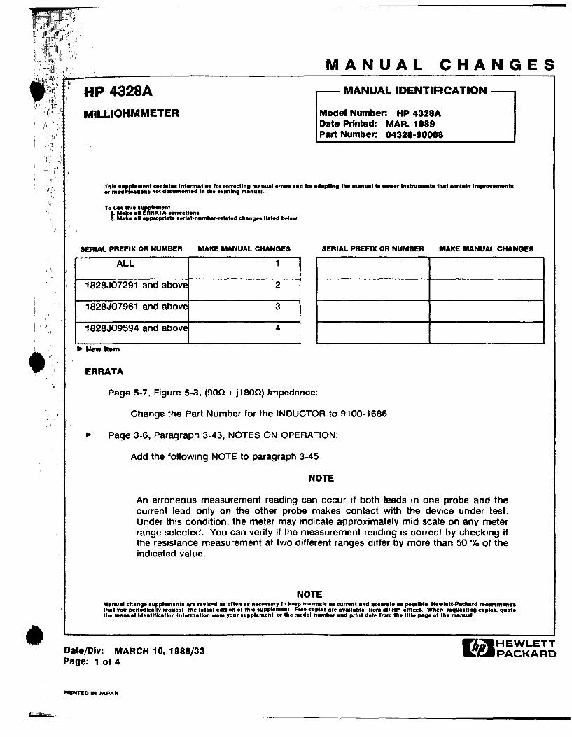
MANUAL CHANGES
HP 4328A
MILLIOHMMETER
r-- MANUAL IDENTIFICATION -
Model Number: HP 4328A Date Printed: MAR. 1989 Part Number: 04328-90008
Thl1 1upr.lomonl eontalno Information for correcting manual erron and for adapting tho manual to nowor lnotNmonle thai oonlaln lmprovomonto or modH calion• not documented In tho oxletlng manual
fo uM thll •upplemont 1 .. Make all ERRATA correction• 2 .. Mako all appropriate .. rial-number-related change• listed below
SERIAL PREFIX OR NUMBER MAKE MANUAL CHANGES SERIAL PREFIX OR NUMBER MAKE MANUAL CHANGES
ALL 1
1828J07291 and above 2
1828J07961 and above 3
1828J09594 and above 4
.., New Item
ERRATA
Page 5-7. Figure 5-3, {900 + j1800) Impedance:
Change the Part Number for the INDUCTOR to 9100-1686 .
.., Page 3-6, Paragraph 3-43, NOTES ON OPERATION:
Add the followmg NOTE to paragraph 3-45 ..
NOTE
An erroneous measurement reading can occur if both leads 1n one probe and the current lead only on the other probe makes contact with the device under test. Under this condition, the meter may mdicate approximately mid scale on any meter range selected. You can verify i! the measurement readmg 1s correct by checking if the resistance measurement at two different ranges differ by more than 50 % of the indicated value.
NOTE Manual change supplements are revised as often as necesury to keep manuals •• current and accurate •• ponlllle Hewlaii-Packard recommend• that you periodically reqUII'SI the latest edition of lhls supplement Free copies are avallallle lrom all HP offices. When requullng coploa. quote the manualldenllllcallon Information rrom your oupplement, or the model number and print dale from the IIIIo page of tho manual .
Oate/Div: MARCH 1 0, 1989/33 Page: 1 of 4
PRINTED IN JAPAN
Flp11HEWLETT ~~PACKARD

,,
L
• Page 5-2, Paragraph 5-13, 4328A PERFORMANCE CHECKS:
Add the following NOTE to paragraph 5-14.
NOTE
Before starting the Performance Check for the 4328A Option 001 , confirm that the battery has enough charge by pressing the BATT. TEST button. If the pointer of meter is out of the BAT. CHARGED range on the meter scale, recharge the battery following the instructions given in Paragraph 3-9. The 4328A Option 001 will not operate properly, if the battery does not have enough charge.
CHANGE 1
..,. Section 6, Replaceable Parts, Table 6-2, Reference Designation Index:
See Table 1, Parts Information.
CHANGE 2
Section 6, Replaceable Parts, Table 6-2, Reference Designation Index:
See Table 1, Parts Information.
Page 4-7, Figure 4-5 and Page 8-19, Figure 8-17, A2 PHASE-SENSITIVE AMPLIFIER Assy.:
Change the value of R230" to 56k0.
Page 8-21, Figure 8-19:
Change the value of R3 to 33k0.
Page 8-23, Figure 8-21:
Change the value of R3 to 33k0.
CHANGE 3
Page 6-8, Table 6-2, Reference Designation Index:
See Table 1, Parts Information.
Page 8-17, Figure 8-14: A3 OSCILLATOR Assy.
Change the value of R335 to 133kn.
- 2-
--- ---~~-~-- ---··~-~----------------
'
•

Page 6-5, Table 6 ·2, Reference Designation Index:
See Table 1, Parts Information.
Page 4-7, Figure 4-5 and Page 8-19, Figure 8-17, A2 PHASE-SENSITIVE AMPLIFIER Assy.:
• Change the value of R234 to 3.16kn-
• • 3 •

'II
I
I'
I
'I
CHANGE
1
2
3
4
PAGE NOTE
6-7 ... c
6-11 ... c
6-5 D
A
6-11 D
A
D
A
6-8 D
A
6-5 D
A
"': NEW ITEM A: Added D: Deleted C: Change
Table 1 . Parts Information
REFERENCE HP DESIGNATION PART NUMBER
A3Q312 1853-0314
F1 2110-0234
* A2R230 0698-3161
* A2R230 0698-5635
DS1 1450-0566
DS1 1450-0613
R3 0683-4735
R3 0683-3335
A3R335 0683-1545
A3R335 0698-3451
* A2R234 0757-0439
* A2R234 0757-0279
I L -4-
DESCRIPTION
TRANSISTOR: SILICON
FUSE SLOW BLOW 100mAT
R: FXD 38.3k!l 1% 1/8W
R: FXD 56k!l 1% 1/8W
LAMP: INDUCTOR
LAMP: INDUCTOR
R: FXD COMP 471<0 5% .25W
R: FXD COMP 33k0 5% .25W
R: FXD COMP 150k0 5% 1/4W
R: FXD COMP 1331<01% 1/8W
R: FXD 6.811<01% 1/8W
R: FXD 3.16k0 1% 1/8W

·t~.·"'' r ~ I I f' ,,, I'
OPERATING AND SERVICE
•
•
MODEL 4328A
MILLIOHMMETER
SERIALS 18:.'8J06-t21 AIHJ ABO\/E
See Sect• on VII for Other Serial Prefixes .
"~' COPYRIGHT YOKOGAWA HEWLETT·PACKARD, LTD 1967 9-1, TAKAKURA.CHO, HACHIOJI-SHI, TOKYO, JAPAN
Manual Part No. 04328-90008 Microfiche Part No. 04328-90058
MANUAL
Prmted : MAR 1989
Ff/OW HEWLETT ~~PACKARD

Table o[ Contents Model 4328A
TABLE OF CONTENTS
Section Page
I GENERAL INFORMATION . . . . . . . . . 1-1 1-1. Description ...................... 1-1 1-9. Accessories Furnished ........... 1-9 1-11. Instrument Identification . . . . , .... 1-2 1-13. Manual Changes .... , ............. 1-2
U INSTALLATION .... , ...... , ............ 2-1 2-1. Introduction . . . . . . . . . . . . . . . . . . . . . 2-1 2-3. Unpacking and Inspection .. , ..... , 2-1 2-5. Storage and Shipment . . . . . . . . . . . . . 2-1 2-6. Packaging .................... ,. 2-1 2-7. Environment . . _...... 2-1 2-8. Installation , . . . . . . . . . . . . . . . . . . . . 2-1 2-10. Combining Case ...... , 2-1 2-12. Adapter Frame , . . . 2-1 2-14. Power Connection . , . . . . . . . . . . 2-1 2-15. Line Voltage . . . . .. . . . . 2-1 2-16. Power Cable . . . . . .. . . . . 2-1
III OPERATION .................. , . . . 3-1 3-1. Introduction . . . . . . .. . . . . . .. 3-1 3 -4.. Controls, Connectors, and
Indicators . . . . . _ . . . . . . . . . . . 3-1 3-6. Battery Operation , .............. 3-1 3-10. Instrument Temperature
Range ...................... 3-1 3-12. Measurement 3-1 3-15. Operating Procedure . . . . . . . . . . . 3-1 3-17. Measuring Voltage on Samples . . . . . 3-1 3-21. Applied Current on Samples and
Ma..ximum Power Dissipation ..... 3-5 3-24. Effect of Series Reactance of
Samples .................... , _ . . . 3-5 3-26. DC Bias Superimposed , . . . . . . ... 3-5 3-30. Recorder Output . . . . . . . . . .. . . . . . . 3-5 3-32. Probe Connection . . . . . _........ . 3-5 3-33. General .......... , . . . . . . . . . 3-5 3-35. Probe InstallatiOn . . . . . . . . . . 3-6 3-37. 16005A Clip-Type Probe . . . . . . 3-6 3-39. 16006A Pin-Type Probe . . . .. . . 3-6 3-41. 16007A B Test Leads .... _ .... 3-6 3-43 Notes on Operation .... , . . . 3-6 3-44 In using the 1 and 3m Ohm
Ranges, Connection o[ Current Terminals to the Sample must be a Firm, Positive Contact . . . . . .. . . . . . . 3-6
3-46. In using the 1 and 3m Ohm Range, Large Electrically Conductive Matedals should not be placed close to the Probe or their Cables 3-6
3-48. Changing Test Lead Length . . . . 3-7
IV THEORY OF OPERATION ............. _ 4-1 4-1. Introduction ,. _ ...... ,. . . . . . . . . .. . . 4-1 4-4. Simplified Functional DescriptiOn 4-1 4-7. Oscillator Circuit . , _ . . . 4-2 4-10. Schmitt Trigger Cucuit . . . . . . 4-2
ii
Section Page
IV THEORY OF OPERATION (Cont'd) 4-12. 20mV Peak Limiter . . . . 4-2 4-14. Phase Sensitive Voltmeter. . . . 4-2
V MAINTENANCE ................. , . . . . . . 5-1 5-l. [ntroduction . , ................... 5-1 5-3. Contents . . . . . . . . .. . . . . . . 5-1 5-4. Performance Checks .......... 5-1 5-6. Adjustments ..... _ ........... , 5-1 5-9. Test Equipment ...... , . . . .. . 5-1 5-11. Maintenance .......... ·-······. 5-2 5-13. 4328A Performance Checks . . . . . .. . 5-2 5-15. Mechamcal Meter Zero . . . .. . 5-2 5-17. Linearity Check ............ , . 5-2 5-18. Full Scale Check . .. . .. . . . 5-2 5-19.. Cover Removal and Replacement. 5-2 5-21. Top Cover Removal .. . . . . . . . . . 5-2 5-22. Top Cover Replacement . . . . 5-2 5-23. Bottom Cover Removal .. , ..... 5-3 5-24. Bottom Cover Replacement 5-3 5-25. Adjustment Procedures . . . . . . . . . . 5-3 5-27. Mechanical Meter Adjustment .. 5-3 5-28. DC Power Supply Check 5-3 5-30. Bias AdJustment , ... , ...... _ .. 5-3 5-32. T302 Adjustment ........... , _ ... 5-3 5-33. Oscillator Output Adjustment .. 5-3 5-34. Electrical Zero Adjustment . . . 5-3 5-35. Lmeanty Adjustment ......... 5-3 5-36. Full Scale Adjustment ........ 5-4 5-37. Recorder Output Adjustment ... 5-4 5-38. Reactance Component Offset
Adjustment ........ ,. . ... , , . . . . 5-4 5-39. Isolating Trouble in Transistor
Circuits ..... , . . . .. . . 5-5 5-40.. General . . . . . . . . . . . .. . . . , . . . 5-5 5-41. In Circuit Testing ............. 5-5 5-45. Out-of-Circuit Testing ........ 5-5 5-47. Component Replacement m
Etched Circuits ................. 5-5 5-48. General . .. . . .. . .. . 5-5 5-49. Axial-Lead Components , . . . . . . 5-5 5-51. Other Components 5-5
Vl REPLACEABLE PARTS . . .. .. . .. 6-1 6-1. Introduction ..... , . . . . . 6-1 6-4. Ordering Information _ .... , . . . . . . 6-1
VII MANUAL CHANGES AND OPTIONS . . . .. . .. 7-1 7-l. Options . . . .. . . ...... _ ............. 7-1 7-3. Special Instruments . . . .. . . . . . .. . . 7-1 7-5. Manual Changes .............. , . 7-1 7-7. Later Instruments . . . . .. . . . 7-1 7-8. Earlier Instruments . , . . . . . .. 7-1
VIIl TROUBLESHOOTING AND CffiCUlT DIAGRAMS , ..... , . . . . . . . . . . .. 8-1 8 -1. Introduction . . . . . . . . .. . . . . .. 8-1 8 -5.. Troubleshooting 8-1 8-8. Schematics . . . . . . . . .. . . . . .. . .. . . . . 8-1
'
-----
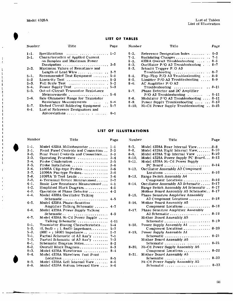
Model 4328A LLst of Tables List of Illustration
LIST OF TABLES
Number Title Page
1-1. 3-1.
3-2.
5-l. 5-2 5-3. 5-4. 5-5.
5-6.
5-7. 6-L
Specifications ...... , . 1-2 Characteristics of Applied Current
on Samples and Maximum Power Dtssipation .............. ,. . . .. . . 3-5
Ma..ximum Values of Resistance and Length of Lead Wire ....... , _ . .. . . 3-7
Recommended Test Equipment .... , ... 5-1 Linearity Test ............ , .. , ...... 5-2 Full Scale Test , .............. , ... , . 5-2 Power Supply Test .......... _. . . . _ .. 5-3 Out-of-Circuit Transistor Resistance
Measurements ........... , ......... 5-6 Safe Ohmmeter Range for Transistor
Resistance Measurements 5-6 Etched Circuit Soldering Equipment .. , 5-7 Ltst of Reference Designators and
Abbreviations ..... , ... , . . . , ........ 6-1
Number Title
6-2. 7-1. 8-1. 8-2. 8-3.
8-4. 8-5. 8-6.
8-7.
8-8. 8-9. 8-10.
Reference Designation Index ....... , .. Backdating Changes .. , ..... , ..... . 4328A Overall Troubleshootmg .... . Oscillator P/0 A3 Troubleshooting . Schmitt Trigger P,'O A3
Troubleshooting , .......... _ .... , -Flip-Flop P/0 A3 Troubleshooting . Limitter P/0 A3 Troubleshooting . , .... AC Amplifier P/0 A2
Troubleshooting .. , ........... . Phase Detector and DC Amplifier
P /0 A2 Troubleshooting . Modulator P iO A2 Troubleshooting Power Supply Troubleshooting .... , .. , Ni-Cd Power Supply Troubleshooting ..
Page
6-2 7-1 8-5 8-7
8-7 8-9 8-9
8-11
8-11 8-11 8-13 8-15
LIST OF ILLUSTRATIONS
Number Title Page
1-1. 3-1. 3-2. 3-3. 3-4. 3-5. 3-6. 3-7. 3-8. 3-9. 4-1. 4-2. 4-3. 4-4.
4-5.
4-6.
4-7.
5-l. 5-2. 5-3. 7-1. 7-2. 8-1. 8-2. 8-3. 8-4.
8-5. 8-6.
Model 4328A Milhohmmeter . . . . . . . . . . 1-1 Front Panel Controls and Connectors . . 3-2 Rear Panel Controls and Connectors... 3-3 Operating Procedure . . . . . . . . . . . . . . . . 3-4 Probe Combmation ..... , . . . . . . . . . . . . 3-5 Probe Installation ...... ,. . . . . . . . . . . . . 3-6 16005A Clip-type Probes . . . . . . . . . . . . . 3-6 16006A Pin-type Probes ..•.... , ...... 3-6 16007A 1B Test Leads ................ 3-6 4-Terminal Device Measurement.... . . 3-7 Basic Low Resistance Measurement ... 4-1 SimphfLed Block Diagram,....... . . . . . . 4-1 Operation of Phase Detector .... _ . . . . . 4-2 Model 4328A Oscillator Talking
Schematic .... , . . . . . . . . . . . . . . . . . . . 4-5 Model 4328A Phase-Sensitive
Amphher Talking Schematic . . . . . . . 4-7 Model 4328A Power Supply Talking
Schematic .... , _ ..... , ............ 4-9 Model 4328A Ni-Cd Power Supply .... .
Talking Schematic . . . . . . . . . . . . . . . . 4-11 Transistor Biasing CharacteristLcs ... , 5-4 (0. 9m.f2 + j 1. 8m0) Impedance ......... 5-7 (900 + J 180Q) Impedance .. , .......... 5-7 Partial Schematic of A2 Ass'y . . . . . . . . 7-1 Parhal Schematic of A3 Ass'y ........ 7-2 Schematic Diagram Notes... . . . . . . . . . . 8-2 Overall Block Diagram. . . . . . . . . . . . . . . 8-3 Model 4328A Waveforms . . . . . . . . . . . . . 8-4 Model 4328A Waveform Test Point
Locations . . . . . . . . . . . . . . . . . . . . . . . . 8-5 Model 4328A Left Internal VIew . . . . . . . 8-6 Model 4328A Bottom Internal V'lew . . . . 8-6
Number Title Page
8-7. 8-8. 8-9. 8-10. 8-11.
8-12.
8-13.
8-14.
8-15.
8-16.
8-17.
8-18.
8-19.
8-20.
8-21.
Model 4328A Rear Internal View ........ 8-8 Model 4328A Right Internal View ....... 8-10 Model 4328A Top lnternal View ....... 8-10 Model 4328A Power Supply PC Board ... 8-12 Model 4328A Ni-Cd Power Supply
PC Board ......................... 8-14 Oscillator Assembly A3 Component
Locations ........................ 8-16 Range Switch Assembly A4
Component Locations .............. 8-16 Oscillator Assembly A3 Schematic ..... 8-17 Range Switch Assembly A4 Schematic .. 8-17 Mother Board Assembly A5 Schemattc .. 8-17 Phase Sensittve Amplifier Assembly
A2 Component Locations .....•..•.. 8-18 Mother Board Assembly A5
Component Locations .............. 8-18 Phase Sensitive Amplifier Assembly
A2 Schematic ............ , ....... 8-19 Mother Board Assembly A5
Schematic ...•......•..........•.. 8-19 Power Supply Assembly Al .......... .
Component Locations .............. 8-20 Power Supply Assembly Al
Schematic ........................ 8-21 Mother Board Assembly A5
Schematic ........... , ............ 8-21 Ni-Cd Power Supply Assembly A6
Component Locations .............. 8-22 Mother Board Assembly A5
Schematic _ ......... _ ....... _ ..... 8-23 Ni-Cd Power Supply Assembly A5
Schematic . . . . . . ........... , ...... 8-23
iii

Section I Paragraphs L-1 to 1-10
SECTION I
GENERAL INFORMATION
1-1. DESCRIPTION
1-2. The Model 4328A Milliohmmeter (Fig. 1-1) is a portable instrument designed to measure low resistance with speed and accuracy. Covering a resistance range of. OOH2 to 100!1, the mstrument uses a Kelvin Bridge method to obtain high sensitivtty Although the 4 terminal method is used to insure accuracy, only 2 probes placed on each end of the sample are used m the actual measurement.
1-3. To avoid measurement errors due to thermal emfs, contact potential differences and electrolytic polarization, the measurement utilizes a 1kHz :::ilgnal and is msensitive to d .. c errors. '
1-4. In the measurement of contact res1stance of components used in low level s1gnal circuits, swttches., relays and connectors, the measurement voltage applied should be less than 20m V peak so that thm insulating films are protected from breakdown With the 4328A, voltage across samples 1s less than 200t.tV peak on any range (when proper range setting used)., and a maximum voltage of 20mV if incorrect range settings are used.
1-5. The 4328A can be used to measure heat-sensitive
__ . .-------
AIHIGE
I -.,'""!-
"' ':l
:.~.-----,. -u,,
samples because the power dissipatwn in samples is very low. Voltage applied to samples is automahcally llm1ted to permit safe measurement of fuses and explosives
1-6. A unique phase dLscriminator in the meter circuit_ insures accurate measurement of samples with senes reactance up to twLce full scale reststance ..
1-7. 150V superimposed de bias may be present on samples durmg measurement. Thus, direct measur~ ment oi mcremental resistance of back biased diodes may be performed, permithng use of the 4328A in the design of semiconductor circuitry.
1-8.. Complete specifications of the Model4328A are given in Table 1-1.
1-9.. ACCESSORIES FURNISHED
1-10 Model 16005A Clip-type probe, 16006A Pintype probe and 16007A B Test Leads are furnished; these probes or test leads may be "mtxed or matched" in any configurahon determined by the form of the sample to be measured.. Also detachable power cord is supplied with the .. Model 4328A Milliohmmeter ..
""•TT rrcr '
LlliE
Figure 1-L Model 4_328A Milliohmmeter
1-1

Section [ Paragraphs 1-11 to 1-14
1-11. INSTRUMENT IDENTIFICATION
1-12. Hewlett-Packard uses a two-section ninecharacter (OOOOJOOOOO) or eight-character (000-00000 or OOOJOOOOO) serial number. The first three or four digits (serial prefix) idenhfy a series of instrument; the last five dig'its identify a particular instrument in that series. A letter placed between the two sections identifies the country where the mstrument was manufactured. The serial number appears on a plate located on the rear panel. All correspondence with HewlettPackard Sales/Service Offices with regard to an instrument should refer to the complete serial number.
1-13. MANUAL CHANGES
1-14. This manual provides operating and service information for the HP Model4328A a portable instru-
Model 4328A
ment for measurement of low resistances. Information in this manual applies directly to instruments (as manufactured) with serial numbers prefixed by the three digits indicated on the title page. If the serial prefix of the instrument is above that on the htle page, a "Manual Change" sheet supplied will describe changes which Will adapt this manual to provide correct coverage. Techmcal correction (if any) due to known errors in print are called Errata and are shown on the change sheet.. And if the serial prefix or number of the instrument is below that on the title page, see SECTION VU MANUAL CHANGES AND OPTIONS. For information on manual coverage of any HP instrument, contact the nearest HP Sales i Service Office (addresses are listed at the rear of this manual)
Table 1-1. Specifications
Resistance Range: 0. 001 to 100 ohms in a 1, 3, 10 sequence.
Resolution rna...:, resolution 0 .. 02 on 0-1 scale. 0. 05 on 0-3 scale.
Accuracy: ±2% of full scale.. Accuracy is un-affected by series reactance of samples with magnitude of up to 2 times full-scale resistance value.
Measuring Frequency: 1000Hz ±100Hz
Voltage across sample:: 200J.N peak at full scale.
Maximum voltage across sample: 20mV peak in any case.
Measuring current and power dissipation in sample.
Range *Applied ~* Ma..ximum Dissipation (ohms) Current (rnA in Samples (J..lW)
0 .. 001 150 23 0.003 50 8 0.01 15 2. 3 0.03 5 0.8 0. 1 1.5 0.23 0. 3 0.5 0 .. 08 1 0.15 0 .. 023 3 0.05 0.008
10 0 .. 015 0.0023 30 0.005 0.0008
100 0.0015 0.00023
* Constant for each range. ** Proportional to meter deflection, full scale
values given.
Superimposed DC: 150V de ma..ximum may be superimposed on samples from an external source.
Recorder Output 0. 1 V de output at full scale meter deflection. Output resistance approx:. 1k ohm.
Operating Temperature Range: 0 to 55°C,
Power:: 115 i230V ±10%, 50 to 60Hz, 2 W Op-
1-2
tional rechargeable battery provides up to 15 hours continuous operation.. Automatic battery recharge.
Weight 7 lbs (3. 2kg)
Accessories Furmshed · 16005A Clip-type Probes 16006A Pin-type Probes 16007A Test Lead 160078 Test Lead Detachable Power Cord 16143A Probe Cable
Accessories Available· 5060-0797 Rack Adapter Frame (holds three instruments the size of the 4 3::!8A. 16459A Carrying Case 1 L056A Handle Kit
Combining Cases. l051A 11 - 1"4 in. (286mm) deep 1052A 16 - 3 8 in .. (416mm) deep The combining cases accept the 1/3 -module HP instruments for bench use or rack mounting. See 1051A data sheet for detail.
Options: 001: Rechargeable battery mstalled, provides up to 15 hours continuous operatmg.
Dimensions:
hiOTE
OIMEI\I:SIOI~IS IN 11~1 HE5 ANIJ IMILLIMETEA:il
liD FOR TOTIIL LENGTH II·ICLUOIIIG 11NOB:i ADO J!5 !l2 1201
f@ FOR HEIG:HT lhiCI UOihiC FEET .1100 T lti II II
'fiDE
_l_
n-------n®
1 " • •. 1'91
ll-----IJJ
.b Bl l'
l-----s-li-••301---1
•-
'
~
- ~
~.
·~ -+·:,1
'~.
i ;)•': '•<~,':·:·
,'1,'/,'','
,, ,,
-'
., , ..
,---='!
' ~
~
~
~
K
2 )
,f / ,f
inltn-
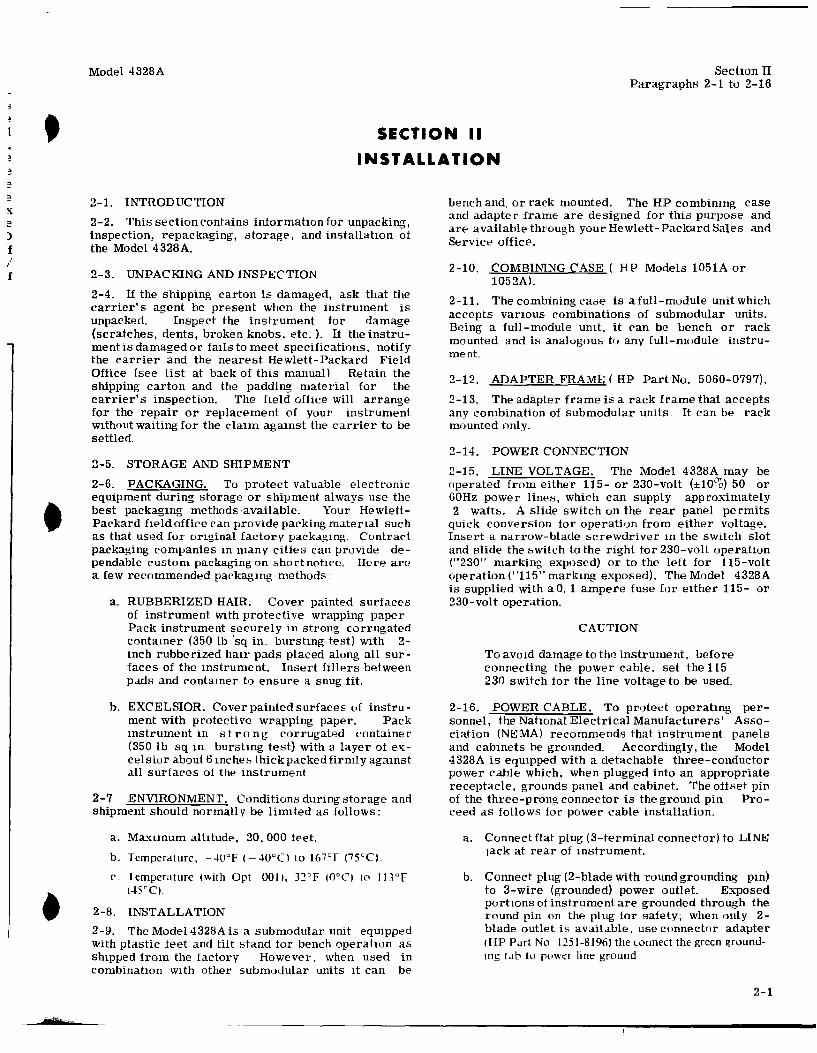
Model 4328A Section IT Paragraphs 2- L to 2-16
SECTION II
INSTALLATION
2-1. INTRODUCTION
2-2. This section contains information for unpacking, inspection, repackaging, storage, and installation of the Model 4328A.
2-3. UNPACKING AND INSPECTION
2-4. If the shipping carton is damaged, ask that the carrier's agent be present when the instrument is unpacked.. Inspect the instrument for damage (scratches, dents, broken knobs, etc .. ). If the instrumentis damaged or falls to meet specifications, notify the carrier and the nearest Hewlett-Packard Field Offlce (see List at back of thLs manual) Retain the shipping carton and the padding material for the carrier's inspection.. The held office will arrange for the repair or replacement of your instrument Wlthout waiting for the cla1m agamst the carrier to be settled.
2-5.. STORAGE AND SHIPMENT
2-6. PACKAGING. To protect valuable electronic equipment during storage or shipment always use the best packagmg methods available. Your HewlettPackard fleldoffice can provide packing matenal such as that used for original factory packaging. Contract packaging companies m many cities can provide dependable custom packaging on short nohce.. Here are a few recommended packaging methods:
a.. RUBBERIZED HAIR. Cover painted surfaces of instrument with protective wrapping paper Pack instrument securely in strong corrugated contamer (350 lb sq in .. bursting test) with 2-inch rubberized hair pads placed along all surfaces of the instrument. Insert fillers between pads and contamer to ensure a snug fit.
b. EXCELSIOR. Coverpaintedsurfaces of instrument with protective wrapping paper.. Pack instrument in strong corrugated container (350 lb sq in .. bursting test) with a layer of ex:celsior about 6 mches thick packed firmly agamst all surfaces of the instrument.
2-7 ENVIRONMENT. Conditions during storage and shipment should normally be limited as follows::
a. Ma..xLmum altitude, 20, 000 feet.
b .. Temperature, -40°F ( -40"CI to l67°F (75°C) ..
c .. Temperature (with Opt. 001), 32°F (0°C) to ll3°F (45°C)
2-8. INSTALLATION
2-9. The Model4328A is a submodular unit, equipped with plastic feet and tilt stand for bench operation as sb1pped from the factory However, when used in combination with other submodular units 1t can be
bench and, or rack mounted. The HP combinmg case and adapter frame are designed for this purpose and are available through your Hewlett-Packard Sales and Service office ..
2-10. COMBINING CASE ( HP Models 1051A or 1052A)
2-11. The combining case is a full-module unit which accepts varwus combinations of submodular units. Being a full-module umt, it can be bench or rack mounted and is analogous to any full-module instrument ..
2-12. ADAPTER FRAME ( HP Part No. 5060-0797).
2-13.. The adapter frame is a rack frame that accepts any combination of submodular units.. It can be rack mounted only ..
2-14. POWER CONNECTION
2-15. LINE VOLTAGE. The Model 4328A may be operated from either 115- or 230-volt (±1000) 50 or 60Hz power lines, which can supply approximately 2 watts. A slide switch on the rear panel permits
quiek conversion for operation from either voltage. Insert a narrow-blade screwdriver in the switch slot and slide the switch to the right for 230-volt operatwn ("230" marking exposed) or to the Left for l15-volt operation ("115" markLng exposed). The Model 4328A is supplied with aD. 1 ampere fuse for etther 115- or 230-volt operation ..
CAUTION
To avotd damage to the instrument, before connecting the power cable, set the 115 230 switch for the line voltage to be used.
2-16. POWER CABLE. To protect operating personnel, the Natwnal Electrical Manufacturers' Association (NEMA) recommends that instrument panels and cabinets be grounded.. Accordingly, the Model 4328A is equipped with a detachable three-conductor power cable which, when plugged into an appropriate receptacle, grounds panel and cabinet. The offset pin of the three-prong connector is the ground pin Proceed as follows for power cable tnstallation.
a. Connect flat plug (3-terminal conneetor) to LINE Jack at rear of instrument.
b. Connect plug (2-blade with round grounding pm) to 3-wire (grounded) power outlet Exposed portions of instrument are grounded through the round pin on the plug for safety; when only 2-blade outlet is available. use connector adapter (HP P.1rt No 1251-8196) the connect the green grounding tab to power !me ground
2-1

I ,,,, '' Model 4328A Section m Paragraphs 3-1 to 3-19
I " ,,
'I"
i r" !
SECTION Ill
OPERATION
3-L INTRODUCTION
3-2. The Model4328A IS effective in measuring contact resistance such as in relays, switches, connectors and incremental resistance of diodes, or lead resistance of integrated circuits. Measurement is made by the 4 terminal method, actually utilizing on 2 probes One current lead and one voltage lead are incorporated in each probe. The probes are branched off through a connector in the probe cord that leads from the front panel and the user can rearrange the different kinds of probes OT test leads at will, according to the form of the sample. This section includes a complete de scription of the Mill iohmmeter operating controls, its accessories, characteristics and techniques of uses ..
3-3. The range of 4328A extends from 1 milliohm to 100ohms full scale in a 1, 3, 10 sequence. Maximum sensitivity IS 20p. ohms.
3-4. CONTROLS, CONNECTORS AND INDICATIONS
3-5. The front and rear panel controls, conneetors and mdicators are explained in Figure 3-1 and 3-2, The descriptions are keyed to the corresponding items which are i.nd'lcated on the fi.gure
3-6. BATTERY OPERATION
3-7. The HP 4328A Option 001 can operate from a rechargeable Nickel-Cadmium battery or ac hne power. Continuous battery operation is poss1ble for approximately 15 hours after a full charge .. The 4328A automatically operates on 1ts mternal batteries whenever the ac lme power IS disconnected, and the batteries are continually charging when the power cable is connected to the power lme, when the LINE lamp is lit
3-8, Before operatmg the 4328A on battenes, check the battery voltage with the BATT. TEST button .. When the BATT TEST button is pressed, the pointer of mater indicates the internal battery voltage .. If the pointer is in the range of BAT. CHARGED of the meter, the battery voltage is h1gh enough to use .. If the pointer IS out ot the range of BAT CHARGED, the battery must be recharged first..
3-9, The battery can be charged using the following procedure (when in the BAT.. CHARGED range or out of the BAT CHARGED range)
I) Connect the power plug to the ac hne, and set the LINE sw1tch to FAST CHARGE.. The LINE lamp is lit and mdicates the battery 1s charging ..
2) Charge the battery unul the pointer is in the range of BAT. CHARGED by pressmg the BATT. TESL It takes apprmumately 4 hours to charge up a full discharged battery mto the BAT CHARGED range, and takes approxImately 48 hours to fully charge ..
CAUTION
The four Nickel-Cadmium batteries in the Option 001 are m hermetically-sealed containers Under high temperatures (above 50° C), hydrogen m the hermetically-
sealed battery container can build up to high pressure causing damage to the batteries and or the mstrument The user must be cognizant of temperature ex:tremes while charging the batteries. Do not charge batteries when temperature is above 40°C ..
3-10 Instrument Temperature Range
3-11, Model4328AOption001 has certain temperature limitations_ Operatmg temperature upper limits for battery operation are lower compared with conventional ac operatwn (Oo C to 50° C). Internal temperatures in ex:cess of 50° Care quite easy to obtain tf the instrument is left m the sun, even if the air temperature is quite moderate A good practice is to be certain that the instrument IS not stored or operated in direct sunlight to avoid the possibility of reduced performance. Keep this limitatwn in mind when operating in field conditions to obtam safe and stable operation.
CAUTION
Nickel-Cadmium cells in this instrument are hermetically-sealed Damage to cells may occur if exposed to extremely high temperatures (above 50° C)
3-12. MEASUREMENT
3-13. Measurement is made by the 4 terminal method to obtam accurate measurement of Low resistance, actually two 2-termmal probes are used so that operatton of the instrument is quite easy The probes furnished in Model4328A are 16005A probe, 16006A probe and 16007 A/B conventional 4 termmal test leads.
3-14. Under no conditions will voltage across the sample exceed 20mV peak, even in the case of incorrect range settings. When the correct range setting is used, voltage across the sample is less than 200f.1V peak. For optimum use of the instrument, range should be set on a higher range when making the mitial connection followed by swttching the selector to the appropriate lower range.
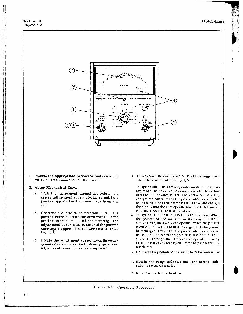
3-15. OPERATING PROCEDURE
3-16. Figure 3-3 illustrates operating procedure.
3-17. MEASURING VOLTAGE ON SAMPLES
3-18. When the voltage applied between the contact is high, the oxidized film formed between the contact is destroyed thereby, and the resistance value me asured may be smaller than under actual use. Moreover, once this happens, it wi.ll never recover the former conditwn even if the voltage or the current is cut off
3-19. According to the recommended standard of IEC (lnternahona Electrotechnical CommissLOn), measurement of contact rest stance by ac should be conducted
3-1

Section III Figure 3-1
..,._ ..... -
C@m HEWLETT PACitARD
1. LINE-ON/OFF.'FAST CHARGE: Instrument power ON/OFF/FAST CHARGE toggle switch connects either ac line or internaL battery (option 001 only) to internaL voltage regulator circuit and provides fast charge to the battery.
2 LINE lamp: This pilot lamp glows when the instrument is turned ON. In optwn 001, the pilot Lamp glows when power cord is connected to ac 115 1 230V source when power switch is in ON or FAST CHARGE positions. When the pilot lamp glows ( Optwn 001 ) batteries are charging continuously.
3. BATT. TEST: Push on~'off switch (non-lock) -a battery test Is made when the push button is depressed irrespective of the position of the ON 10FF·FAST CHARGE switch.
4. RANGE: Low resistance measurement range selector; seLect ranges from lm!J fuLt scale to 1000 fuLl scale.
10 ,. •••
BATT .. TESr 3
~--~~------~2 LINE
OFF fAST CHAitti:E
Model 4328A
5. PROBE: Cord, for measurement, divides into 2 probes at moduLar connector.
8_ CAUTION
Superimposed DC voltage limits are as folLows:
(1) Between High and Low terminals ±150Vdc maximum.
(2) Between Low terminal and GND ±500Vdc maximum.
Do not superimpose DC voltage above sample limits.
6. MechanicaL Meter Zero: Sets meter suspension so that meter indicates zero. To adjust the zero.
a. Remove power from the instrument.
b. Turn the adJustment screw cLockwise until the indicator falls beLow zero and comes back up to zero again.
,1,
I • I
t·
c. Turn the adjustment very slightly counter- • clockwise to free up the mechanism from the adJUSti.ng peg.
Figure 3-1. Front Panel Controls and Connectors
3-2

Model 4328A
1. Line Fuse· Select fuse to match line voltage m u.se. For 115V ac or for 230V ac use 0. 1 amp slow blow fuse ..
2.... Power Cord Input: Use power cord provided, (HP 8120-1378) Line Power limits are 115/ 230V ac, 50 - 60Hz.. Check FUSE rating and position of -Une voltage slide switch before connecting power.
3 .... Line Voltage Slide Switch: Set to line voltage available (115 or 230V ac, 50 - 60Hz)
Section III Figure 3-2
4 .. RECORDER OUTPUT· 0 ... 1 V de output is obtamed at full scale meter deflection directly proportional to meter deflection Output impedance is approximately 10000.
5. Cabinet Ground:: The recorder output is normally floating and Cabinet Ground termmal is tied to earth ground... When recorder output 1s connected to the input of the recorder and when the recorder cabinet is not hed to earth ground, the recorder cabinet should be connected to th1s Cabinet Ground terminal.
Figure 3-2. Rear Panel Controls and Connectors
3-3
Section Ill Figure 3-3
1. Choose the appropriate probes or test leads and put them into connector on the cord.
2. Meter Mechanical Zero.
a. With the instrument turned off, rotate the meter adjustment screw cLockwise until the pomter approaches the zero mark from the left.
b. Continue the clockwise rotation until the pomter coinctdes with the zero mark. [f the pointer overshoots, continue rotating the adjustment screw c lockw1se until the pointer once again approaches the zero mark from the left.
c. Rotate the adJustment screw aboutthree degrees counterclockwise to disengage screw adjustment from the meter suspension.
Model 4328A
3.. Turn 4328A LINE switch to ON .. The LINE lamp grows when the instrument power is ON ..
In Option 001: The 43~8A operate'> on Its mternal battery when the power cable is not connected to ac Ime and the LINE switch IS ON. The 4328A operates and charges the battery when the power cable IS connected to ac !me and the LINE switch is ON. The 4328A charges the battery and does not operate when the LINE switch ism the FAST CHARGE position.
4 In Option 001:: Press the BATT. TEST button When the pomter of the meter is in the range of BAT.. CHARGED, the 4328A can operate .. When the pointer is out of the BAT.. CHARGED range, the battery must be recharged .. Even when the power cable i'> connected to ac line, and when the pomter is out of the BAL CHARGED range, the 4328A cannot operate normally until the battery Is recharged .. Refer to paragraph 3-9 for details
5. Connect the probes to the sample to be measured.
6. Rotate the range selector until the meter indicator moves on scale.
7. Read the meter indication.
Figure 3-3. Operatmg Procedure
3-4
A Model4328A
by means of measuring instruments with voltage peak values of 20mV or less.
3-20. The instrument can not start oscillating H no sample is connected between the probes .. When sample is connected between the probes, a positive feedback loop is formed, and the oscillator begins oscillation. Since constant current flows in the sample (in correct range setting), voltages across the sample are proportional to sample resistance and are less than . 2m V peak on any range, at full scale deflection. When the resistance value of the sample is greater than that of the set range, an "over-voltage" protection circuit ln the Model 4328A i.s called upon to prevent any voltage higher than 20mV peak from belng applied to the sample.. Thus, when an unknown sample IS measured without special preparation, contact resistance is still accurately measurable without disturbance to the contact points.
3-21. APPLlED CURRENT ON SAMPLES AND MAXIMUM POWER DISSIPATlON
3-22. With Model 4328A, the current and power applied to samples are extremely small, the maxima at measurement (i. e, when the meter needle deflects full scale) being as shown in the table below.
Table 3-1. Characteristics of Applied Cur-rent on Samples and Maximum Power Dissipation
MEASURING *1 POWER *2 RANGE CURRENT DISSIP A TlON (Ohm) (rnA) (/lW)
0. 001 150 23 0. 003 50 8 0.01 15 2.3 0.03 5 0.8 0 1 1.5 0.23 0. 3 0.5 0 .. 08 l 0 .. 15 0 .. 023 3 0 .. 05 0.008
10 0. 015 0. 0023 30 0 .. 005 0.0008
100 0.0015 0.00023
* 1 Constant to each range.
*2 Propo-rtional to meter deflection, against full scale deflectwn ..
3-23. As shown in the above table, the power dissipation at sample is so small that fuses, detonators and semi-conductors can be safely measured.
3-24 EFF.Ii:CT OF SERlES REACTANCE OF SAMPLES
3-25. The meter circuit of Model 4328A does not (within limits) respond to the series reactance of --a sample. The meter mdtcates only the correct value of the pure resistance of the sample as long as the series reactance of the sample at 1kHz is less than twice full scale resistance value.
3-26. DC BIAS SUPERIMPOSED
3-27 DC bias may be present on samples, due to
Section III Paragraphs 3-20 to 3-34
some source. Model4328A measures with ac (1kHz), but its probe ctrcuits incorporate de blocktng capacitors The mstrument will not burn out nor will any measuring error will occur even when the probes come in direct contact With a de circuit. The maximum de voltage applicable between two probes is 150V.
3-28.. Also, as the probes are floating from the instrument case (able to Withstand voltage up to 500V de; insulation resistance 10Mr2 or over), it is possible to measure the resistance value of a sample having de voltages relative to ground by connecting directly to it.
3-29. The dynamic resistance of elements whose V-1 characteristics shownon-hnearittes, (such as diodes) may be measured at an arbitrary DC bias pomt. In this type of measurement, note that the maximum voltage (1 kHz) applied to the sample is 0. 2mV peak or less ..
3-30. RECORDER OUTPUT
3-31. A RECORDER termmal is provided on the rear panel of the 4328A, providing a de voltage proportional to the resistance of the sample permitting recording of consecutive tests, etc.
3-32. PROBE CONNECTIONS.
3-33. General
3-34. In Model 4328A, measurement is made by the 4-terminal method; special two-terminal probes that can make 4-terminal measurements (16005A Cliptype Probes and 16006A Pin-type Probes), and conventional4-terminal testleads (16007 A/B Test Leads) are furnished, and can be mixed or matched depending on sample type For eKample, in the case of measurement of the contact resistance of printed circuit board connectors, 1t is usually convenient to use a combination of the clip-type probe and the pin-type probe as shown in Figure 3-4.
Figure 3-4. Probe Combination
3-5

Section III Paragraphs 3-35 to 3-46
3-35. Probe Installati.on
3-36.. Plug in the probes to the connector at the end of 16l43A Probe Cable. Note that the probe plugs must be oriented correctly before plugging m.
1) Connector at the end of probe cable has 4-contacts Each pairof closely--spaced contacts comprise one set of probe contacts.
2) Plug the probe pms in to the connector such that the off set Side faces outwards.. Refer to Figure 3-5.
t 16143A
Figure 3-5. Probe Installation
3-37. 16005A CLip-type Probe
3-38. General purpose, alligator-jaw contacts provide positive gripping of samples. Upper contact (marked "V"l is voltage termmal and lower contact is current terminal. When using this probe in 1 mn range, It is not alway-s possible to measure the sample because of extreme deflectwn of the meter. Figure 3-6 shows 16005A Clip-type Probes.
Figure 3-6. 16005A Clip-type Probes
3-39. 16006A Pin-type Probe
j /
3-40. Probe tip is a voltage terminal and outer conductor ts a current terminal. Probe tip is springloaded, so that both terminals firmly contact the sample under test. This probe LS usefulfor press-an contact measurement such as printed board conductivity measurements. When using this probe m lmn range, itis notalways possibleto measure the sample because of extreme deflection of the meter. (See Figure 3-7).
3-6
---.jo._--~-.~- __ L+_,._-.._._,j...
Model 4328A
Figure 3-7.. 16006A Pin-type Probes
3-41. 16007A!B Test Leads
3-42.. These are provided for standard 4 -terminal measurements.. Each pair of testlead has a separate alligator clip voltage and current terminaL 16007A is furnished with a red cover the 16007B with a black cover.. The black test lead is the voltage terminal and the grey test lead IS the current terminaL (See Figure 3-8)
Figure 3-8.. 16007A/B Test Leads
3-43. NOTES ON OPERATION
3-44.. IN USING THE 1 AND 3m OHM RANGES, CONNECTION OF CURRENT TERMINALS TO THE SAMPLE MUST BE A FIRM, POSITIVE CONTACT.
3-45.. With Model 4328A, the internal resistance of the constant current generator is approximately-equal to the set range x500 Therefore, at 1m ohm and 3m ohms ranges, the internal resistances are 500m ohms and 1. 5 ohms respectively.. Excessive resistance at the probe contact can therefore relatively larger error than on other ranges, The quahty of the connection of the probes to the sample may be deterrowed by applying pressure on the connection point and noting if the meter needle deflects.. Very poor contact or no contact whatsoever 1s mdicated by- a deflection off-scale
3-46.. IN USING THE 1 AND 3m OHM RANGE LARGE ELECTRICALLY CONDUCTIVE MATERIALS SHOULD NOT BE PLACED CLOSE TO THE PROBES OR THEIR CABLES,

r:-·· 1
••
Model 4328A
3-47. On the 1 and 3m ohm ranges, currents flowing in the current leads are 150 mA and 50 rnA respectively large compared to other ranges. Moreover, the voltmeter sechon has very high sensitivity, so that, if a conductor surface is placed near and parallel to the current loop, large errors may result due to coupling between the current loop, the conductor and the voltage terminals. Therefore, at 1 and 3m ohm range, the probes and their cables (i.e. the part between the connector and the tip of probe) must be placed lOcm or more away from the conducting surface or the probes must be placed perpendicularly to the conductor face ..
3-48. A 4- terminal measurement ts a method by which resistance is accurately measured by removing the effect of thermal emf and Lead wire resistance. If a 4-termmal device is measured with the 4-terminal method (Figure 3-9, a), the reading of the indtcating meter will be an Rx which is accurate. However, when measuring resistance by ustng only two terminals of a 4-terminal device (as shown in Figure 3-9, b) the meter will show the resistance of Rx + 2Re. Thus an error of 2Re/Rx results in this instance. If Rx is much larger than Re (Rx/Re> 1000), the error wtll be withm specifications (±2%) even if measuring resistance wtth the method shown in Figure 3-9b.
3-49. CHANGING TEST LEAD LENGTH.
3-50. The values in Table 3-2 are given for wire lengths from the tip of test lead plug to the other end of lead wire, and are maxtma for a single lead.. Note that BOTH the resistance of lead wire AND the wire length must be kept within the values shown in Table 3-2 at the same time.. Further it is recommended that the 4 lead wires be used in a bundle as far as is possible .. The wire length and wire quality of the other two kinds of probes should not be changed.
4-TERMINAL DEVICE
VOLTAGE TERMINAL
(a)
CURRENT TERMINAL
s Rx MEASURED RESISTANCE.
Section III Paragraphs 3-47 to 3-50
Table 3-2. Maximum Values of Resistance and Length of Lead Wire
Range Lead Wire Lead Wire (ohms) Resistance Length (em)
(ohms)
0.001 0.002-0.02* 40
0.003 0 06 60
0.01 0.2 100
0.03 0.6 200
0.1 2 200
0.3 6 200
1 20 200
3 20 200
10 20 200
30 20 200
100 20 200
• Mimmum to maximum value shown.
4- TERMINAL DEVICE
.~ ~ 1 VOLTAGE :TERMINAL I
\ I CURRENT I TERMINAL I
r I I
(b)
Re RESISTANCE OF LEAD OR TERMINAL.
Ftgure 3-9. 4-Terminal Device Measurement
3-7

--Model 4328A Section IV
Paragraphs 4-1 to 4-6
SECTION IV
THEORY OF OPERATION
4-1. INTRODUCTION
4-2. The measuring princtple of Model 4328A is, as shown in Figure 4-1, the so -called 4-terminal method, where constant current i Is applied to a sample Rx, and the voltage drop VR is measured. If 1 IS known, andresistance valueRx maybe calibrated linearly on a voltmeter scale. By changing i, range changing is possible
r.c. r,.
r;,
R)) Rx
Flgure 4-1. Basic Low Resistance Measurement
4-3.. This method requires a total of 4 terminals to be connected to the ends of sample Rx, L e , one voltage and one current terminal on each end. The set of
HIGH INPliT r-------1 IMPEDANCE
AMP
20mV PEA~
LIMirTER
POWER
AMP
·f111
current terminals applies constant current 1 to sample Rx, the voltage terminals detect the voltage drop across Rx. Using this method, the resistance of the lead wires, and the contact resistance between terminals and sample will not constitute any error. The effect of the resistance of voltage terminals rv is removed by making the internal resistance of the voltmeter (MV) sufficiently greater than rv. Resistance rt of the current terminals can also be ignored, as it is normally sufficiently less than the internal resistance R of constant current source. In Model 4328A, the internal impedance as seen from voltage terminals is set at 5k0 or higher, and the internal resistance of constant current source is set at RANGE x500.
4-4. SIMPLIFIED FUNCTIONAL DESCRIPTION
4-5. Functionally vtewed, Model 4328A may be divided into two major sections. One is the 1kHz oscillator sectlon serving as constant current source; and the other is a voltmeter section of the phase-discriminator type amplifying the voltage drop across the sample, synchronously rectifying tt and deflecting the ohm-calibrated meter.
4-6 The following is a detailed description of operationof the 4328A refering to Figure 4-2, Model 4328A Block Diagram.
lli•Rx+JXr
V •V"R+V'x.
----Curr Tip
v.
MODULATOR DC
AMP
PHASE
DETECTOR
FLIP-FLOP
SCHMITT
--, I I
L---------------------------------------------------~~DETECTOR __ _J
TRIGGER
Figure 4-2 .. Simplified Block Diagram
4-1

' ' " I
' ~ I I
:I II,
Sectwn IV Paragraphs 4-7 to 4-17
4-7 .. OSCILLATOR CffiCUIT
4-8.. Assuming that a sample with a resistance value Rx is connected between the current terminals only, a closed current loop is formed bv Reference Resistance Rs of the instrument, Rx and secondary winding of Output Transformer Tl. A positive feedback loop is formed as Rs is connected to the mput terminal of High Input Impedance Amp I ifier, and through It to the Power Amplifier of the next stage and the Output Transformer T 1. This loop Will oscillate depending on the range setting (Rs value). The oscillation frequency, which IS determined by capacity Co and inductance Lo of T1, is 1kHz ±100Hz ..
4-9. The value of Rs is selected by RANGE switch, to be 500 times full scale RANGE value. Th.is oscillator acts as a constant current source, as viewed from sample Rx. Also, the voltage VI at both ends of Reference Resistance Rs is always 100mV peak, thus, when the value of Rx is equal to full-scale value, the 1kHz voltage applied to Rx wlll be 0. 2mV peak. In other words, the voltage applied to the sample is of a verv low level, 0. 2mV peak or lower, at normal measurement. The input impedance of High Input Impedance Amplifier is set sufficiently high so that Rs is unaffected by it.
4-10. Schmitt Trigger Ctrcuit
4-11. When the value of sample Rx is greater than set range, or specifically, Rs 2 Rx, the loop gain of this positLve feedback loop becomes 1 or smaller, so thatoscillation stops .. (f the voltage terminals are connected to both ends of sample Rx at this time, the voltage drop at both ends of Rx is zero. A trigger circuit is added to cause the meter needle -to read above full-scale whenever the value of Rx IS greater than the set range. In other words, when the oscillator's power decreases to below a certain level, the Schmitt Trigger circuit provides a DC voltage to the DC Amplifier m the input stage of the Meter, causing it to deflect off-scale,.
4-12. 20mV Peak Limiter
4-13. The 20mV peak Limiter connected to the current termmals limits the a. c. voltage applied to the sample to 20mV peak.. It does this by comparing the 1kHz output level to a reference diode. When a given level is exceeded, the 1kHz signal is amplified and rectified and the resultant de level is used to reduce the oscillator gain
4-14. PHASE SENSITIVE VOLTMETER
4-15. When the current terminals and the voltage terminals are connected to the sample Rx (It is assumed that the range-setting of 4328A at this time is correct), the voltage drop at both ends of Rx is applied to AC Amplifier via Input Transformer T2, where it is amplified Its output IS connected to the input of the Phase Detector. The other input of the Phase Detector is driven by a Flip- Flop driven by 1kHz from the oscHlator section. That is, the output signal of the AC Amplifier IS synchronously rectified by a voltage which is in-phase with the current flowing in the Reference Resistance Rs (L e .. current flowing in sample Rxl. Thus, a sample Zx = Rx + ]Xx, the voltage
4-2
Model 4328A
drop across the sample will be v = VR + jvx The Input of the AC Amplifier will also be the voltage drop vx whose phase differs from vR by 90°. The Phase Detector detects only the voltage drop vR which is in phase with the current in Rs and provides DC voltage output proportional to vR only.. Therefore, no error is present i.n the meter reading due to Vx, or effectively, the reactance Xx gives rise to no error.
lt 1/x, It r- -,
I I I RK I I
Zx I I I I I I I I Xx I I I I .... L _J I
I
.. I
VR (a) (b)
Flip-Flop
(c)
11'1 IR I I ' VR' -M-M-LF-1 I ' 1
Vx=O
Figure 4-3. Operation of Phase Detector
4-16. The dynamic ranges of the AC Amplifier and Phase Detector of the next stage are sufficiently great that errors due to X11: will be less than 100 as long as the value of reactance Xx at lkHz does not exceed twice the range setting This is an important feature, espectally with reference to AC measurement of low resistance where1n the series inductance component in the sample is a sigmftcant part of the total ac impedance.
4-17 DC signal VR which was synchronously rectified by Phase Detector is amplified and appHed to the Modulator of the next stage This Modulator has two inputs and one output -an AC signal vR corresponding to the product of VR (proportional to the resistance value Rxl and the 1kHz AC signal v3 (which is in phase with the current ln Rs) The AC output signal vR is
II Ill~~ " I
'" ,' ,,,',
i - ~ I I'' 'I,

A
1-
'P ~e
m
d t s d
v t
Model 4328A
negatively fed back to the mput of the AC Amplifier. Therefore, even if the oscillator's output should change, the meter indication will not budge. The voltage drop VR across the sample changes, but v3 also changes at the same rate .. The relation vR = v'R remams constant. Stable operation is obtained, as the entire eire mt of this voltmeter section is incorporated within the negative feedback loop.
4-18. The output VR of the DC amphfler 1s also applied to the Meter and Recorder termtnals.. VR and v' R are related linearly .. The response of the Recorder output requires 0. 6 second to reach 90%of the final reading.. Recorder output is 0 .. 1 V at full scale.
Section IV Paragraph 4-18
4-3

Model 4328A
--- --- --- ---- i
•
r--tLIPPER---,
F1gure 4-4, ModEl 4328A Osnllator Tctlking Schematic
Section IV Figure 4-4
~-;=-....,_,.;Ill-~ ,"''lrJJ ~~ .. ~ .... ...,. ... ,.,...,., .,..,_,,,.,..,,..,,.._,.nn liDliiUIJIJIIIrDII 1,..,.
4-5

-
SEE INSIDE
Figure 4-4
MODEL 4328A OSCILLATOR TALKING SCHEMATIC
4- 5

Model 4328A
·~·-·--~ ~
l!liiLe..:o...---'11
Ill' -r~ .... '"'"' ""'*' Wll .. ~·I"'.__ • .,+., h- ..-1
.
' "
Phllfll ULJO"ftll AI'"'~'
_.._..,""""'"""'-·--llt:ll'tu tl'! '--1-fft ••- WI
.. .._"_,_,,._lin -~ 11!-- := =>=';~
r,:-::C,.-A:-,..,.-------L.::-~===f~IQ:!06A andQ~OiiB am.plll~ Holl.:l..EF dllfLrt-nrr= ,., lhtooulpul3ollhtPha=F Dfelrrlor ~ RZJ:I eommon emlll!!rre.:l.;dor;;uppllu con:.l::!.nl tllrnnllnQ:ZOfiA Q201iB Q10bB Q201 ;and Q20i! a.rnpllh roU:q;:e dille renee::: bEI~~f'n I he n::cll- ;u- oulpul 1."1 dr l:"ouph:d lo Q20B Q:.!OB t!mlller lrJIIown pnnldE:: lul'l lmp!'dilnrr lalnr nulpul 1'1il i201, :and Uw ll.t: oulpuf of Q;!O!l modublor 1 lit oufpul tn Q;!09 l.IKI dtliFE rap.lblllllt!!! CR.i!O<I ruuples Q::!OB nulpul dlre~:IIV fo T:l02 Q:ZOJ I:;=. hh;:h lmj::-;::dii.n<:c: ;:.,rr<=nl :;-;::;,.n::;:: l:ir hlfh am- mEit~r co:..,(,-, :h-I , (I (~.,I ;:;I :;-::.._(;:::) .. 1-;;::,., ~-::h.---,111 Ttlf:r;:>=o lit::;; R2Jl I:; 11-.e piiiiEt commvn ~q~= rEIErlhln CR1n11~ ill-f-mpnalurr- con 1- n!41ar tallbrJ.Inr llm;arlly adru.:l R:!ll9 IE lh" m£1H lull :niL a.dru=l CfHO<l pton_;;-:!llon lor Ql!lll Q201 oulplll );J a~: ~oupiEd lo Q204 high rorreetll lor I hE r-omblnEd non-llnnrll~ ul modulalor and ITWII"r 1 lrcull A.<!:i!ll
.-----+J.c~:_--Jt~l;7 a~ii~I~:.U,~~~:a~lt•:~:~'!!: Q~£~~~~~~:;, p~!! ~~~:~~~~~c~~!:,l ro~~; :~;~1~;mr~~;ilu~ppu~~~~;~Ea;~~~~u..:R107 :ldJLCilTIEnl lxl'nEn Flip Flop outpula :uu1 1\C ;~mpiiiiEr lnpul r~mpllll5allnn lor Q109 C::!IJ IQ=~a rlpplt low
li:t::-====:'_ _______ ft"'Ir 1"""',,
!-b_ .. ,,,tr;~ .. ~.:':!'--- ------- I -------- ---- ---- ----
~ I'MIU~--I;DI!;ITM.,..A;ntlfAirtll).l1.;,-~------ ------------------- -------- -
1--------, ~CTlltJIII<IAI!DiPo~'YIP43:!!1-TDUI L"•.c:l ____ --------
1·, i '------fr-4 ..,. ___ _ Clll,l-+1 ____ ...,
I I! ::I
"'--------8.=..,1,~-~~NIT"I WI IIi -;-.-'"'---r---4,,.+- ....
I I:
'-----t---t---l-----t----1:• ••b-- ro ~YI I 'I
i i! --------- _=-:=J~•~; u~
I
------------ I Ill ____________ ,'------- ------------------- ----------~
1,.,.,..,,,1'~•· •u~-~ ... ..,111 .. ,~~..._,,n
Ftgure 4-5 Morlel 4Jl!MA Phase-Sensitive Amplifier Talking Schematic
Section IV Figure 4-5
4-7

S!E INSI DE
Figur e 4-5
MODEL 4328A PHASE - SENSmVE AMPLIFIER TALKING SCHEMATIC
4- 7

~~·-'~'
. ' '
PnFTI-tli
Bridge circuli:~ CRJOfl CRJO'i CRltlll c:;JO) lorm a lull '«I&V£ bridge rFcllller Tn lhls ur~menl fwo n-oct111f'TI! open.!~> In serle: on each
0 h:lll nil he c,d~, one red IllEr b.=lng In 1he lea.o 10
Ill£ la:u:l I he ulher belllj\" In Uw relurn le3d CJOJ lteep;; ripple low
f
I
I ,_,_,_
I
~-·~ I' CRJJO prutldt>!i a r-Eiarem:e ~allage lor I hE (-J:l\1) ]JO'A<I'T
:L -~---------, r'ftur- 1------- .I
L------~~-~~~FI~c~R~JO~·~~~~p~ll:oo~b~I~~-~,,~,,~'~";~~=~R~J~IU------l_-T--+---~ ,4 ' ~' ------""----ll,"'""""--"'' .. fj ., ...... 11,1-l
L-------------------------7~ r~ L_ _________________ ~------'o' :, : 0
! ,-----""-""----if-~-, ............. , ....... ,_q,# I -Tf1tQI-IAM
L -------- ---------------------------------------------------------------------
I !_________ ----------------------------------- ------- ------------------- ----------- ---------~--- ---
' L_______J__~-'cJ_,>-----=-_j
i 1_111 = --==--&allll,LI I
F1gure 4-6, Model 4328A Power Supply Tallung Schemat1c
4-9

SEE INSIDE
Figure 4-6
MODEL 4328A POWER SUPPLY TALKING SCHEMATIC
4-9

Model 4328A
Brljge rlrc.Jit, CR48l. CR402. CR-l03. CR4J< ~r.d
;;~.:~.\~\~~~- ~:~~~·.·~~~;:"_.,::~~ :;,l.l'i-"'-T--'~"'----; ,,.,.~, .. ,.~. "~------.. •1~\~~~·,~~-~~:~:~"~:,h~ ~~:..~~:~ 10 ~4~~1 "-.J---~ " i<<>"?t. rippl• luw
Q"'""'~-...
.
' •' I
I
Figure 4-7. Modrol 4328A Ki-Cd Power Supply Talking Schemalic
Section IV Figure 4-7
p~=~--~
~i;,, I
I I
I
4-11

SE! INSIDE
Figure 4-7
MODEL 4328A NI-Cd POWER SUPPLY TALKING SCHEMATIC
4-11
•.

Model 4328A Section V Paragraphs 5-1 to 5-10
SECTION V
MAINTENANCE
5-1. INTRODUCTION
5-2. This section outlines routme maintenance, performance checks, adjustments, calibratLon and troubleshooting for the 4328A Milliohmmeter. Performance checks may be used on incoming inspection to verlfy instrument specifications.. The performance checks should also be used alter any adJustments have been made ..
5-3, CONTENT
5-4. PERFORMANCE CHECKS
5-5. The performance check procedures will ver1fy Milliohmmeter performance during incoming inspection, periodtc evaluation, calibration and troubleshooting. The tests can be performed without requiring removal of the access instrument case. Specifications in Table 1-1 are the performance standards. Should the Milliohmmeter fails to meet any of the per[ormance test specifications, refer to the troubleshooting diagrams.
5-6. ADJUSTMENTS
5-7.. The adjustment procedures describe the adJustments necessary to calibrate the Milliohmmeter. AdJust the Model 4328A only when it is determined that the instrument is actually out of adjustment, and not malfunctioning due to a circuit failure ..
5-8. Several circuit components are factory-selected to meet specific c trcuit requirements.. The factory selected parts are indicated on the schematic diagrams ..
5-9. TEST EQUIPMENT
5-10. [nstruments and accessories required for adjusting and testing the 4328A are listed and briefly described in Table 5-1. Instruments used to check 4328A performance must meet or exceed the spectftcations given ..
Table 5-1. Recommended Test Eqmpment.
lnstrument Type Required Characteristics Use Recommended Model
0. 001 to 100 ohms Full scale checks YEW Type 2782 or YEW
Standard Reslstor Accuracy ~ ±0.1% and calibration Type 2792 and GR-1433-U Decade resistor
Decade Range: 10 to 100 ohms Tracking checks & YEW Type 2786 or
Reststance Box Accuracy: ±0.1% calibration at lOOn GR Model 1432T range Decade Resistance Box
Ohm Meter Range: 1n Troubleshooting HP Model 412A Accuracy: ±5%
Digttal Range:: O.lV Troubleshooting HP Model 3440A Voltmeter Accuracy: ±0.2%
DC Voltmeter Range:. 1 - 30V
Checks HP Model 412A Accuracy: ±1%
100/lV· em Checks and HP Model l80A
Oscilloscope Vert. Sens. Vert. Plug-in Sweep time 0. 5 ms. "em Troubleshooting Model 1806A
5-1

Section V Paragraphs 5-11 to 5-22
5-11. MAINTENANCE
5-12. Service information m the form of troubleshooting, waveforms, schematics and component locations are given m Section VIII. Also, an overall system block diagram is included which contains keyed numbers correspondmg to the test points.
5-13. 4328A PERFORMANCE CHECKS
5 -14.. The performance checks presented here are front panel operations designed to compare the Model 4328A wlth its published specifications These operations should be conducted before any attempt is made at instrument calibration or adjustment During performance tests, periodically vary the Une voltage supplied totheModel4328A, ±:1000on eitherll5 or230 V operation A 1/4 hour warm-up period should be allowed before these tests are conducted.
5-15. MECHANICAL METER ZERO.
5-16. If necessary, mechanically zero the meter movement as follows.
a.. With instrument turned off, rotate meter adjustment screw clockwise until pointer approaches zero mark from the left.
b. Continue rotatmg clockwise until pointer comcides with zero mark. If pointer overshoots, continue rotating adjustment screw clockwise until pointer once again approaches zero mark from the Left.
c. Rotate adjustment screw about three degrees counterclockwise to disengage itfrom the meter suspension
5 -17.. LINEARITY CHECK
a.. Attach the Model16005A probe to the 4328A and set the range switch to 100R
Table 5-2. Linearity Test
Standard HP Model HP Model Decade 4328A 4328A Resistor Meter Range Settmgs Readings Settings
on 0
10 8 - 12
20 18 - 22
30 28 - 32
40 38 - 42
50 48 - 52 won 60 58 - 62
70 68 - 72
80 78 - 82
90 88 - 92
100 98 - 102
5-2
Model 4328A
b.. Connect the Model 4328A probe to the Decade Resistance Box ( YEW Type 2792 or GR Model 1432T)
c.. Switch the Decade Resistor, providing 0 to 1 00&1, in 10n steps.
d.. The Model4328A should read as shown in Table 5-2.
5-18 FULL SCALE CHECK
a Attach the Model 16007AiB Test Lead to the Model 4328A.
b Connect the Test Leads to Standard Resistor of 0 .. 001 to lOOn and check the full scale readings of the Model 4328A. The Meter should read as shown in Table 5-3.
5-19. COVER REMOVAL AND REPLACEMENT
5-20. The side covers can be removed and replaced independently of the top and bottom cove r.s. Each side cover 1s held in place by four screws retamed by nuts whlch are fastened to the side frames.
5-21. TOP COVER REMOVAL
a. At the rear of the instrument, remove the screw that retams the cover.
b. Grasp the cover from the rear, and slide it back 1 · 2 inch.. Then tilt forward edge of the cover upward and hft the cover from the instrument ..
5-22 TOP COVER REPLACEMENT
a. Rest the cover flat on the cast guides projectlng mward near the top of each side frame.
Table 5-3.. FuLl Scale Test
Standard HP ModeL HP Model Resistor 4328A 4328A
Meter Range Readings Settings
0 .. 001 f.! 0. 00098 - 0 .. 00102 r2 0 .. 001 n t ( 0 003 0 00294 - 0 .. 00306 0 .. 003)
0 .. 01 0.0098 - 0 .. 0102 0 .. 01
0.03 0.0294 - 0.0306 0 .. 03
0 .. 1 0 .. 098 - 0.102 0. 1
0 .. 3 0.294 - 0 .. 306 0 .. 3
1 0 .. 98 - 1. 02 1
3 2. 94 - 3.06 3
10 9 .. 80 - 10 .. 2 10
30 29 .. 4 - 30.6 30
100 98.0 - 102 0 100
* YEW TYPE 2872 only.

,,
I iili
,,
j
Model 4328A
b. Slide the cover forward, allowmg its forward edge to enter the groove in the front panel.
c. Replace the cover retaining screw.
5-23,. BOTTOM COVER REMOVAL
a. Remove the retaining screw at the rear of the cover.
b. Swing the tilt stand out to free the cover.
c. Slide the cover rearward far enough to free the forward edge.
d. Tilt the forward edge of the cover upward and lift the cover from the mstrument.
5-24. BOTTOM COVER REPLACEMENT
a. Set the tilt stand out of the wav of the cover.
b. Rest the bottom cover flat on the cast guides proJecting inward near the bottom of each side frame.
c. Slide the cover forward on the guides so that the formed portion at the rear of the cover slides over the two short projections at the rear corner of each side frame.
d. Replace the retaining screw ..
5-25. ADJUSTMENT PROCEDURES
5-26. The following is a complete adjustment and calibration procedure for the Model4328A. These operations should be conducted only if it has previously been established by PERFORMANCE TESTS, that the Model 4328A is out of adjustment. If the procedure outlined do not rectify any discrepancy that may exist, and all connections and setting have been rechecked, refer to TROUBLESHOOTING in Section VIII, for possible cause and recommended corrective action.
5-27. MECHANICAL METER ADJUSTMENT
a. When the meter is properly zero -set, the pointer rests over the zero mark on the meter scale when the instrument is:
(1} at normal operating temperature.
(2) in its normal operating position.
(3) turned off.
b. Set the pointer as follows to obtain best accuracy and mechanical stability,
(1) Turn mstrument off.
(2) Rotate the meter mechanical adJustment screw clockwise until the meter pointer is to the left of zero and moVIng up the scale toward zero. Stop when the pointer is exactly over the zero mark. If the pointer
Section V Paragraphs 5-23 to 5-35
overshoots, repeat step 2.
(3) When the pointer is exactly on zero, rotate the adjustment screw approximately 3 degrees counter-clockwise, This frees the adjustment screw from the meter suspension. If the pointer moves during this step, repeat steps 2 and 3.
5-28. DC POWER SUPPLY CHECK
5-29. Refer to Table 5-4 for Power Supply Check points and typical voltage values. Measure de voltage between common and designated Location on MotherBoard. Measure de ±13V ac ripple withOscilloscope (HP Model 140A). The peak value of ripple should not exceed 2mV.
Table 5-4. Power Supply Test
Location on Line Voltage Mother-Board Tolerance Variation
+13V WHT/RED +12V-+14V 103V-127V
-13V WHT -12V--14V
5-30. BIAS ADJUSTMENT
5 -31. With the probe leads shorted adjust R360 so that Q302 collector voltage reads 3. 7V to COMMON. This sets the bias on Q303 base Oscillator output transistor.
5-32. T302 ADJUSTMENT
a. Set the Model 4328A to 1m&1 Range with the probes shorted or 1m&1 across them.
b. AdJust T302 by turning top core cw or ccw for maximum peak reading. Output is taken at T301 terminals marked BLU and BLK.
5-33. OSCILLATOR OUTPUT ADJUSTMENT
a. Set the Model 4328A to 100&1 Range with the probes shorted.
b. AdJust R306 and R360, alternately, for a voltage of 200m Vp-p at T301 terminals marked BLU and BLK (use HP Modell40A).
5-34. ELECTRICAL ZERO ADJUSTMENT
a. Set Model 4328A Range Sw1tch to 100&1,
b. Short the current probes and voltage probes to each other, for zero mput.
c. RotateR228 clockwise slowly and ascertam that the Meter pointer moves up scale, and then rotate counterclockwise until pointer reaches "just" zero.
5-35. LINEARITY ADJUSTMENT
a. Set Model 4328A Range Sw1tch to lOOn.
5-3
Section V Paragraphs 5-36 to 5-38
b. Put the Model16005A Probes or l6007A/B Test Leads to the Model 4328A.
c. Connect the probes to Standard Decade Resistance Box YEW Type 2786 or GR Model 1432T.
d. Adjust the Decade Resistor to provide 30!'2, and adJust R232 so that the pointer mdicates 30n.
e. Adjust the Decade Resistor to provide lOOn, and ad)ust R229 so that the Meter indication is toon.
f. Set Decade Resistor to provide 10 to lOOn in order and check the tracking tolerance of Model 4328A. It should be ±0. 500.
g. If the tracking is out of tolerance, repeat d, e, and f.
5-36. FULL SCALE ADJUSTMENT
a. Attach the Model 16007A/B Test Leads to the Model 4328A.
b. Connect the Test Leads to Standard Resistor of 0. 001 to 100n and check the full scale readings of the Model 4328A.
c. The Meter Readings should be within ±0 .. 5'lQ of full scale.
Model 4328A
d. If the readmgs are off, values of RlOl to Rll1 should slightly be changed for adJusting U1e full scale.
5-37. RECORDER OUTPUT ADJUSTMENT
a. Set the Model 4328A Range Switch to lOOn and connect the probes to 100!'2 Standard Resistor. Check the full scale readmg of the ModeL 4328A.
b. Adjust A2R233 for the recorder output to be lOOmV de between terminals marked RECORDER on the rear panel.
c. Repeat Paragraphs 5-35, 36 and 37.
5-38. REACTANCE COMPONENT OFFSET ADJUSTMENT
a. Set the Model 4328A range to 1m!'2 and measure an impedance of (R + jwL) as shown in Figure 5-2, where R should be calibrated by DC bridge and the reactance value twice that of R.
b.. AdJust A2C208 as the error should come within ±1 o relative to the calibrated value. A2C207 is changed to different values when A2C208 is out of range.
c Set the 4328A range to 3mn and check with Standard Resistor. If necessary adjust A4R102*, error should be within 1%.
TRANSISTOR BIASING DEVICE SYMBOL CUT OFF CONDUCTING
PLArE +200V +200V
VACUUM TUBE GRID-$ -15V~ -JV~ CATHODE
COLLECTOR +20V +20V
BASE~ ~MAIN N P N TRANSISTOR DV~ +.3 V /CURRENT
(OR-) :-CONTR
EMITTER CURRENT -::-
COLLECTOR -20V -20V
~SE~ ~MAIN P N P TRANSISTOR ov(> -.3 V YURRENT
(OR+) -= CONTR
EMITTER CURRENT -=
Figure 5-1. Transistor Biasing Characterlstlcs
5-4
I
* I'' t
f
!
~
,,
I ,, -
I
'I
~I·'
I '',
' ,, ,,'
,,

F
I !
~· I
i
~·
Model 4328A
d. ALL ranges should be checked with Standard Resistors and adjusted if necessary. A4R101 *, 102*, 109*, 110*, 111*, and 117* through 122~' are all factory selected.
e. Set the range to 1000 and measure an impedance of (R + jwL) as shown in Figure 5-3, where R should be calibrated by DC bridge and the reactance value twice that of R.
f. A~ust C202 as the error should come within ±1 •O relative to the calibrated value (Note: C202 takes value from 0. 015 - 0. 025 tJF).
g. Check again at 1mn range whether the error is in the above specification.
5-39. ISOLATING TROUBLE IN TRANSISTOR CIRCUITS
5-40. General. The following information should help determine is a transistor works. There are tests for both in-circuit and out-of-circuit transistors, which help to determine If a particular trouble is due to a faulty transistor or some other component. See Figure 5-l.
5-41. In-Circuit Testing. Intransistor circuit testing the most important consideration is the transistor base-emitter junction. Like the control gndof a vacuum tube, this is the control point in the transistor.
5-42. To check atransistor, first seeif the emitterbase dwde is forward-biased by measuring the voltage difference between emitter and base. When usmg an electronic voltmeter, do not measure directly between emitter and base; there may be sufficient loop current between the voltmeter lead to damage the transistor. Instead, measure each voltage separately with respect to a voltage common point (e. g. , chassis).
5-43. If the transistor base-emitter Junction is forward-biased, the transistor conducts. If the diode is heavily forward-biased, the transistor saturates. However, if the base-emitter diode ts reverse-biased, the transistor is cut off (open). The voltage drop across a forward-biased emitter-base junction varies with transistor collector current. A germanium transistor has a typical base -emitter voltage of 0. 2 - 0. 3 volt with 1 - lOrnA collector current, and 0. 4 - 0. 5 volt with 10 - 100mA collector current. In contrast, base-emitter voltage for silicon transistors is about twtce that for germamum types; about 0. 5 - 0. 6 volt for low collector current, and about 0. 8 - 0. 9 for high collector current.
5-44. If the emitter-base Junctions forward-biased, check for amplifier action by short-circuiting base to emitter while observing collector voltage. The transistor should stop conduction (cut off, which should shift the collector voltage close to the supply voltage. Any difference is due to current leakage through the transistor. In general, the smaller the current, the better the transistor. If collector voltage does not change, the transistor has either an emitter-collector short circuit or emitter-base open circuit.
Section V Paragraphs 5 -39 to 5-52
5-45. OUT-OF-CIRCUIT TESTING
5-46. The two common causes of transistor failure are internal short- and open-circuits. Remove the transistor from the circuit and use an ohmmeter to measure internal resistance. See Table 5-5 for measurement data.
5-47. COMPONENT REPLACEMENT IN ETCHED CIRCUITS
5-48. GeneraL Etched circuit boards are sensitive to heat and to scratches with sharp objects. This is because the conductors are plated on to the circuit boards and the plating extends through the component mounting holes. Whenever possible, avoid unnecessary component substitution; it can damage the circuit board and adjacent components.. See Table 5-7 for recommended tools and materials.
5-49. AXIAL-LEAD COMPONENTS
5-50, Resistors, tubular capacitors and other axial lead components can be replaced without unsoldering. Cutthe componentleads near the bodyof the defective component, remove the component and straighten the leads left in the board. Wrap leads of the replacement component one turn around the original leads, solder the connection, and clip off the excess lead.
5-51 .. OTHER COMPONENTS
5-52. Replace other components as follo'Ys:
a. Remove defective component from circuit board. Use a low-power soldering ironbecause excessive heat may lift a conductor or damage the board.
b. Remove solder from mounting holes with a suetion device or a wooden toothpick. DO NOT USE A SHARP METAL OBJECT SUCH AS AN AWLORTWIST DRlLL. SHARP OBJECTS MAY DAMAGE THE PLATED-THROUGH CONDUCTOR.
c. Shape the leads of the replacement component to match the mounting-hole spacing.
d. Insert the component leads in the mounting holes and position it as the original was. DO NOT FORCE LEADS OF REPLACEMENT COMPONENT INTO MOUNTING HOLES. A sharp edge on the lead rna y damage the plated -through conductor.
e. Solder the component in place andre move excess flux from the soldered areas. Apply a protective coating to prevent contamination and corrosion. See Table 5-7 for recommendations.
5-5
'I I ' I
Section V Table 5-6 and 5-7
Table 5-5. Out-of-Circuit Transistor Resistance Measurements
Connect Ohmmeter Measure Transistor
Resistance Type Pos, Neg. (ohms) lead to lead to
emttter base* 200-250 Small Signal emttter collector lOK-lOOK
PNP Germa-
emitter base* 30-50 nium Power
emitter collector several hundred
emitter base* lOK-lOOK
PNP Small Silicon Signal very higll
emitter collector (might read open)
base emitter 1K-3K
Small very high Signal collector emitter (might
NPN read open)
Silicon base emitter 200-1000
Power high, often collector emitter greater
than 1M
* To test for transistor action, add collector-
5-6
base short. Measured resistance should decrease,
CAUTION
Most ohmmeters can supply enough current or voltage to damage a transistor. Before usmg an ohmmeter to measure transistor forward or reverse resistance, check 1ts open-circuit voltage and short-ctrcuit currentoutputON THE RANGE TO BE USED. Open-circuit voltage must not exceed 1. 5 volts and short-circuit current must be less than 3ma. See Table 5-6 for safe resistance ranges for some common ohmmeters.,
Model 4328A
Table 5-6. Safe Ohmmeter Range for Transistor Resistance
Measurement~
Open Open Ohm- Safe Ckt Ckt
meter Range(s) Voltage Current Color Polarity
RxlK 1. ov lmA
RxlOK l.OV lOOJ.LA HP412A
Rx lOOK l.OV lOJ.LA Red +
HP427A Black -RxlM 1. ov lilA
RxlOM 1. ov 0. lilA
RxlK 1.3V 0.57mA
RxlOK 1.3V 57J.LA + HP410C RxlOOK 1. 3V 5.7J.LA
Red Black -
RxlM 1. 3V o. 5J.LA
RxlOM 1. 3V 0. 05J.LA
RxlOO l.lV l.lmA
RxlK l.lV llOJ.LA
HP410B RxlOK l.lV llJ.LA Black +
Rx lOOK l.lV 1. lilA Red -
RxlM l.lV 0. 11/lA
Simpson RxlOO 1.5V lmA Red +
260 Black -
Simpson RxlK 1.5V 0.82mA Black +
269 Red -
Triplett RxlOO 1.5V 3.25mA
630 RxlK 1.5V 325p.A Varies with Serial
Triplett Rx 10 1.5V 750p.A Number
310 RxlOO 1.5V 75J.LA
1,111
1,"
I
(
,'' ,,,:l
I ~ti C'-"'"1
j,
t

r
I
~
Model 4328A Section V Table 5-7
Table 5-7. Etched Circuit Soldering Equipment
Item Use
Soldering Tool Soldering Unsoldering
Soldering Tip, Solder1ng general purpose Unsoldering
De-soldering aid Unsoldermg multi-connection components (e .. g. , tube sockets)
Resin (flux) Remove excess flux solvent from soldered area
before application of protective coating
Solder Component replacement Circuit boartl repair Winng
Protechve Contamination, corrosion Coating protection after soldering
*Krylon Inc., Nornstown, Pennsylvania
1. CORE
2. COIL
9170-0271
(1. 5mm¢ copper wire one turn)
Figure 5-2. (0. 9mS1 + j 1. 8mr.l) Impedance
Specification Item Recommended
Wattage rating 37. 5 Ungar #776 Handle with Tip Temp 750 - 8oo• F Ungar #1237 Heating Unit Tip Size· 1/8" OD
Shape·· chisel Ungar #PL113 Size 1/8"
Suction device to remove Soldapult by the Edsyn molten solder from Company, Arleta, connection California
Must not dissolve etched Freon circuit base board rna- Acetone tenal or conductor Lacquer Thinner bonding agent Isopropy Alcohol (100% dry)
Resin (flux) core, high tin content (60/40 tin/ lead), 18 gauge (SWG) preferred
Good electrical insula- Krylon* #1302 tion, corrosion-prevention properties Humiseal Protective Coating,
Type 1B12 by Columbia Technical Corp. Woodside 77, New York
1. RESISTOR 0757-0399
2. INDUCTOR 9100-0761
Figure 5-3. (90S1 + j 180n) Impedance
5-7

NOTES
1,,,,,
il' 'I':,
)I
II! ''1,,1
It
I!
I!
II
II' ( ,,,
II
/):
'II
I i
I
II -

Model4328A Section VI Paragraphs 6-1 to 6-6
SECTION VI
REPLACEABLE PARTS
6-1. INTRODUCTION
6-2. Ttns section contains information for ordering replacement parts. Table 6-2 lists parts m alphanumerical order of their reference designators and indicates the description (see Table 6-1 for abbreviations used) and -hp- stock number of each parts, together with any applicable notes.
6-3. Miscellaneous parts associated with each assembly are listed at the end of each assembly listing. Others are listed at the end of Table 6-2.
6-4_ ORDERING lNFORMATlON
6-5. To obtain replacement parts, address order or inquiry to your local Hewlett-Packard Field Office (see lists at rear of tlus manual for addresses). Idenhfyparts by their Hewlett-Packard stock numbers.
6-6. To obtain a part that is not listed, include:
a. Instrument model number.
b. Instrument serial number.
c. Description of the part.
d. Function and location of the part.
Table 6-1. List of Reference Designators and Abbreviations
REFEI!EliiCE DESIGNATORS
A c assembly E mlsc electronlc part p plug v vacuum, tube, neon B motor F ruse Q transistor bulb, photocell, etc. BT c battery FL rmer R resistor VR voltage regulator c capacitor J 1ack RT thermistor w cable CP coupler K relay· s switch X socket CR diode L lnductor T transrormer y crystal DL delay llne M meter m terminal board DS device slgnallng (lamp) MP mechanical part TP test point
ABBREVIATIONS
A amperes H henries NPN negative-positive- RMS root-mean square A. F .. C. automatic t. requency· control HEK he <agonal negatlve RWV reverse working AMPL c amplifier HG mercury NRFR not recommended for voltage
B .. F .. O. beat frequency oscillator HR hour(sl field replacement
S-B slow-blow NSR not separately BE CU c beryllium copper IF Intermediate freq SCR screw BH c binder head IMPG Impregnated replaceable SE sele-nium BP c bandpass INCD mcandescent SECT sectlon(s) BRS c brass INCL lnclude(s) OBD order by descriptlon SEMICON .semiconductor BWO backward wave oscillator INS insulatwn(ed) OH OV'al head S! silicon
INT internal OX o11ide S!L silver ccw counter -clockwise K kilo = 1000 SL slide CER ceramic SPG spring CMO c cabinet mount onlv LH left hand p peak SPL special COEF coefficient LIN linear taper PC printed circuit SST stainless steel COM c common LKWASH lock Wol.Sher PF picofarads = I 0 SR split ring COMP composition LOG logarithmic taper farads STL steel COMPL = complete LPF low pass filter PHBRZ phosphor bronze TA tantalum CONN connector M mill!= I0-3 PHL Phillips TD time delay CP cadmium plate MEG meg= 106 PIV peak tnv·erse voltage TGL toggle CRT cathode -ray tube MET FLM metal film PNP posittve-negati ve- THD thread cw clockwise MET OX metallic oxide positlv·e
TI titanium DEPC deposited carbon MFR manufacturer P/0 part of TOL tolerance DR drive MINAT miniature POLY polystyrene TRIM trimmer
MOM momentary PORC porcelain TWT traveling wav·e tube ELECT • electrolytic MTG mounting POS posltlon(s) ENCAP encapsulated MY "mylar'1 POT potentiometer u micro= 10-6 EXT e>.ternal pp peak-to -peak
F farads N nano (l0-91 PT point VAR c variable
FH c flat head NiC normally closed PWV peak working voltage VDCW de working volts
FILH a fiUister head NE neon Wi with FXD c rtxed N1 PL nickel plate RECT rectifier w watts
N/0 normally open RF radio frequency WIV working inverse GE germanium NPO negative positive zero RH round head or voltage GL glass (zero temperature right hand ww wtrewound GRD ground(edl coefflc lent) HMO rack mount only W'/0 without
6-1

Section VI Table 6-2
6-2
Reference Designation
1.
2.
3.
4.
5.
6.
7.
8.
9 ..
10.
stock No.
5060-0703
1490-0031
5040-0700
5060-0727
5020-6852
5000-8565
5060-8549
5000-8571
04328-1042
04328-10021
Model4328A
Table 6-2, Reference Designation Index
Descnphon Note
CD
FRAME ASSEMBLY
STAND: TIT..T
HINGE
FOOT ASSEMBLY
METER TRIM
SIDE COVER
COVER: TOP
COVER: BOTTOM
PANEL: REAR
PANEL: FRONT
~
'"·-~

r ' '
i
I
~·
j I
~·
Model 4328A
Reference Designation
A1
AlC1-A1C300
A1C301 A1C302 A1C303 A1C304
A1CR1-A1CR300
A1CR301 A1CR302 A1CR303 A1CR304
A1CR305 A1CR306 A1CR307 A1CR308 A1CR309 A1CR310
AlQl-AlQ300
A1Q301 A1Q302 A1Q303
A1Q304 A1Q305 A1Q306
A1R1-A1R300
AlR301 A1R302 AlR303 AlR304
A1R305 A1R306 A1R307 AlR308 A1R309
Table 6-2, Reference Designation Index
Stock No. Description
04304-7043 POWER SUPPLY ASS'Y AC POWER OPERATION ONLY 04304-8704 BOARD: BLANK P. C.
NOT ASSIGNED 0180-0967 C: FXD ALUM 470f.LF 25VDCW 0180-0756 C: FXD ALUM 22f.LF 16VDCW 0180-0967 C: FXD ALUM 470f.LF 25VDCW 0180-0756 C: FXD ALUM 22p.F 16VDCW
NOT ASSIGNED 1901-0230 SEMICON DEVICE: DIODE SILICON 1S1625 600V 350mA 1901-0230 SEMICON DE VICE, DIODE SILICON 1S1625 600V 350mA 1901-0230 SEMICON DE VICE, DIODE SILICON 1S1625 600V 350mA 1901-0230 SEMICON DEVICE, DIODE SILICON 1S1625 600V 350mA
1902-0049 SEMICON DEVICE· DIODE BREAKDOWN 6. 19V 400mW 1901-0230 SEMICON DEVICE· DIODE SILICON 1S1625 600V 350mA 1901-0230 SEMICON DEVICE· DIODE SILICON 1S1625 600V 350mA 1901-0230 SEMICON DEVICE- DIODE SILICON 181625 600V 350mA 1901-0230 8EMICON DEVICE· DIODE SILICON 181625 600V 350mA 1902-0049 SEMICON DEVICE· DIODE BREAKDOWN 6. 19V 400mW
NOT ASSIGNED 1854-0854 TRANSISTOR· NPN SILICON 1854-0003 TRANSISTOR NPN SILICON SIMILAR TO 2N1711 1854-0854 TRANSISTOR: NPN SILICON
1854-0854 TRANSISTOR NPN SILICON 1854-0003 TRANSISTOR: NPN SILICON SIMILAR TO 2Nl 711 1854-0854 TRANSISTOR: NPN SILICON
NOT ASSIGNED 0683-1245 R: FXD COMP 120kfl 500 1/4W 0683-3925 R: FXD COMP 3. 9kfl 500 1/4W 0683-5635 R:: FXD COMP 56kfl 500 1/4W 0683-5635 R:: FXD COMP 56kfl 5% 1,'4W
0683-1245 R:: FXD COMP 120kfl 5% 1/4W 0683-3925 R: FXD COMP 3. 9kr.l 5% 1/4W 0683-5635 R: FXD COMP 56kfo 5% 1/4W 0683-5635 R: FXD COMP 56kfl 500 1/4W 0683-3335 R: FXD COMP 33kr.l 5"b 1/4W
MISCELLANEOUS 5040-3304 HOLDER: CAPACITOR 2 REQ'D
See list of abbreviations m introduction to th1s section
Section VI Table 6-2
Note
6-3
Section VI Table 6-2
Reference Designation
A2
A2C1-A2C200
A2C201 A2C202 A2C203
A2C204 A2C205 A2C206 A2C207* A2C208
A2C209 A2C210 A2C2ll A2C212 A2C213
A2C214 A2C215 A2C216 A2C217 A2C218
A2CRl-A2CR200
A2CR201 A2CR202 A2CR203
A2CR204 A2CR205 A2CR206 A2CR207 A2CR208
A2CR209 A2CR210
A2Q1-A2Q200
A2Q201 A2Q202 A2Q203 A2Q204
A2Q205 A2Q206 A2Q207 A2Q208 A2Q209
6-4
Model 4328A
Table 6-2, Reference Designation Index (Cont'd)
Stock No. Description Note
04328-7022 PHASE SENSlTIVE VOLTMETER ASS'Y 04328-8702 BOARD: BLANK P. C.
NOT ASSIGNED NOT ASSIGNED NOT ASSIGNED
0180-1031 C: FXD TANT 4. 7p.F 20% 15VDCW
0160-1548 C: FXD MY 0. 22p.F 10% 200VJ?CW 0180-1031 C: FXD TANT 4. 7~J.F 20% 15VDCW 0180-1029 C, FXD TANT 1p.F 20% 15VDCW 0160-2204 C: FXD MICA lOOpF 5% 300VDCW 0121-0215 C VAR CER 7-45pF 350VDCW
0180-1031 C: FXD TANT 4. 7~J.F 2000 15VDCW 0180-1029 C _ FXD TANT 1p.F 20% 15VDCW 0180-1031 C: FXD TANT 4. 7~J.F 20% 15VDCW 0160-1554 C~ FXD MY 0. 47p.F 10% 200VDCW 0180-0210 C: FXD TANT 3. 31J.F 20% 15VDCW
0180-1029 c~ FXD TANT 1p.F 20% 15VDCW 0180-1029 C: FXD TANT 1J.LF 20% 15VDCW 0180-1029 C: FXD TANT 1J.LF 2000 15VDCW 0180-1029 C: FXD TANT 1J.LF 2000 15VDCW ~
0160-0127 C: FXD CER lp.F 20% 25VDCW 't' '• I Ill
,'''
NOT ASSIGNED 1901-0040 SEMICON DEVICE: DIODE SILICON 1901-0040 SEMICON DEVICE DIODE SILICON 1901-0040 SEMICON DEVICE: DIODE SILICON
1901-0040 SEMICON DEVICE: DIODE SILICON NOT ASSIGNED '·
1901-0040 SEMICON DEVICE: DIODE SILICON 1902-3150 SEMICON DEVICE: DIODE BREAKDOWN 9. 09V 200 400mW 1901-0040 SEMICON DEVICE.: DIODE SILICON
1902-3150 SEMI CON DE VICE· DIODE BREAKDOWN 9. 09 V 2% 400m W 1902-3172 SEMICON DEVICE DIODE BREAKDOWN ltV 200 400mW
NOT ASSIGNED 1854-0854 TRANSISTOR· NPN SILICON 1854-0854 TRANSISTOR· NPN SILICON 1854-0854 TRANSISTOR· NPN SILICON 1854-0854 TRANSISTOR~ NPN SILICON
1854-0854 TRANSISTOR~ NPN SILICON 1854-0221 TRANSISTOR: NPN SILICON PAIR
NOT ASSIGNED 1854-0854 TRANSISTOR: NPN SILlCON 1854-0854 TRANSISTOR: NPN SILlCON
See list of abbreviations in introduction to this section
' ' L

r. Model 4328A
Reference De,..io-nat1on
A2Rl-A2R200
A2R201 A2R202 A2R203
A2R204 A2R205 A2R206 A2R207 A2R208
A2R209 A2R210 A2R211 A2R212 A2R213
A2R214 A2R215 A2R216 A2R217 A2R218
A2R219 A2R220 A2R221 A2R222 A2R223
A2R224 A2R225* A2R226 A2R227 A2R228
A2R229 A2R230* A2R231 A2R232 A2R233
A2R234* A2R235 A2R236 A2R237 A2R238
-
'
M
Table 6-2, Reference Designation Index (Cont'd)
Stock No. Description
NOT ASSIGNED 0757-0460 R: FXD MET FLM 61. 9kr.l 1'"\J 1/BW 0757-0465 R: FXD MET FLM 100k0 100 1. 8W 0683-1045 R: FXD COMP lOOkn 500 1 i4W
0683-1335 R:: FXD COMP 13k0 500 1,'4W 0683-2035 R: FXD COMP 20k0 500 1 i4W 0683-7525 R: FXD COMP 75000 500 li4W 0757-0460 R:. FXD MET FLM 61. 9k0 100 1 8W 0757-0465 R.: FXD MET FLM 100k0 100 1 '8W
0683-4735 R FXD COMP 47k0 5':1[, 1, 4W 0683-5115 R: FXD COMP 5100 500 1/4W 0683-5635 R: FXD COMP 56k0 5'"'0 1 /4W 0683-6845 R: FXD COMP 680k0 500 1 '4W 0683-7525 R: FXD COMP 75000 5% 1,/4W
0683-1825 R: FXD COMP 1800r.J 6'\'1 1/4W 0757-0960 R: FXD MET FLM 33kO 200 1/8W 0757-0461 R: FXD MET FLM 68.1k0 100 1/8W 0757-0461 R: FXD MET FLM 68. lkQ 1 ~' 1 18W 0757-0960 R: FXD MET FLM 33kQ 2% 1 i8W
0683-1035 R: FXD COMP lOkO 500 1/4W 0757-0465 R· FXD MET FLM 100k0 tOO 1/8W 0757-0465 R FXD MET FLM 100k0 1 Oj', 1 8W 0683-8235 R FXD COMP 82k0 set;', 1 /4W 0683-1045 R · FXD COMP 100kr.! 500 1/4W
0683-2035 R · FXD COMP 20k0 500 1 4W 0698-3160 R: FXD 31. 6kf2 1% U8W 04328-8619 R; FXD W. W. 430 5% 0683-2005 R FXD COMP 200 5% 1 14W 2100-0558 R: VAR 20k!l 10% L 2W
2100-0558 R: VAR 20k!l 10% 1/2W 0698-3161 R: FXD 38. 3kQ 1% 1 8W 0683-4325 R: FXD COMP 43000 5"0 1/4W 2100-3252 R: VAR 5kS? 10% 1/2W 2100-0567 R: VAR 2kf.! 10% 1, 2W
0757-0439 R: FXD 6. 81kQ 1% 1 "BW 0757-0288 R: FXD MET FLM 9. 09kQ 100 1/8W 0683-3025 R: FXD COMP 3kr.! 5'~, 1,14W 0683-2725 R:: FXD COMP 2700r.! 500 1/4W 0683-6815 R: FXD COMP 6800 500 1, 4W
See list of abbreviations in introduction to this section
Section VI Table 6-2
Note
6-5

Section VI Table 6-2
Reference Desi!!nation
A3
A3C1-A3C300
A3C301 A3C302 A3C303
A3C304 A3C305 A3C306 A3C307 A3C308
A3C309 A3C310 A3C311 A3C312 A3C313
A3C314 A3C315 A3C316 A3C317 A3C318
A3C319 A3C320 A3C321 A3C322
A3CR1-A3CR300
A3CR301 A3CR302 A3CR303 A3CR304
A3CR305 A3CR306 A3CR307 A3CR308 A3CR309
A3CR310 A3CR311 A3CR312 A3CR313 A3CR314
6-6
Model 4328A
Table 6-2, Re[erence Designation Index (Cont'd)
Stock No. Description Note
04328-7034 OSCILLATOR ASS' Y 04328-8707 BOARD BLANK P.C.
NOT ASSIGNED 0180-0978 C: FXD TANT 111-F 50VJ)C_F 0180-1029 C: FXD TANT 111-F 20% 15VDCW 0160-1548 C :: FXD MY 0. 22J.J.F 10% 200VDCW
0160-1548 C: FXD MY 0. 22J.J.F 10% 200VDCW 0170-0084 C: FXD MY 0. 06811-F 20% 50VDCW 0180-1029 C: FXD TANT 111-F 20% 15VDCW 0160-1554 C: FXD MY 0. 47tJ-F 10% 200VDCW
NOT ASSIGNED
0180-1029 C: FXD TANT 111-F 20% 15VDCW 0180-1029 C: FXD TANT 111-F 20% 15VDCW 0180-1029 C: FXD TANT 111-F 20'0 15VDCW 0160-0134 C: FXD MICA 220pF 5% 300VDCW 0180-1029 C: FXD TANT 111-F 20% 15VDCW
0160-1563 C: FXD MY 0. 47J.J.F 5% 200VDCW 0180-1029 C: FXD TANT 111-F 20% 15VDCW 0150-0121 C: FXD CER 0. 11J-F -20+8000 50VDCW 0150-0121 C: FXD CER 0.1tJ-F -20+80% 50VDCW 0160-0127 C: FXD CER 111-F 20% 25VDCW
0180-1029 C: FXD TANT 1tJ.F 20% 15VDCW 0160-1542 C: FXD MY 1500pF 10% 100VDCW 0160-1542 C: FXD MY 1500pF 10% 100VDCW 0160-1544 C; FXD MY 4700pF 5% 100VDCW
NOT ASSIGNED 1902-3125 SEMICON DEVICE: DIODE BREAKDOWN 6. 98V 2% 400mW 1901-0040 SEMICON DEVICE: DIODE SILICON 1901-0040 SEMICON DEVICE: DIODE SILICON 1901-0040 SEMICON DEVICE: DIODE SILICON
1901-0040 SEMICON DEVICE: DIODE SILICON 1901-0040 SEMICON DEVICE: DIODE SILICON 1901-0040 SEMICON DEVICE: DIODE SILICON 1901-0040 SEMICON DEVICE: DIODE SILICON 1910-0016 SE MICON DEVICE: DIODE GERMANIUM
1910-0016 SEMICON DEVICE: DIODE GERMANIUM 1901-0040 SE MICON DEVICE: DIODE SILICON 1901-0040 SE MICON DEVICE: DIODE SILICON 1902-3150 SEMICON DEVICE: DIODE BREAKDOWN 9. 09V 2% 400mW 1910-0016 SEMICON DEVICE: DIODE GERMANIUM
See list of abbreviations in introduction to this section

)-
Model 4328A
Reference Desi!mation
A3CR315 A3CR316 A3CR317 A.3CR318 A.3CR319
A.3CR320 A.3CR321 A.3CR322 A.3CR323
A.3Q1-A3Q300
A.3Q301 A.3Q302 A.3Q303 A.3Q304
A3Q305 A3Q306 A3Q307 A3Q308 A3Q309
A3Q310 A3Q311 A3Q312 A3Q313 A3Q314
A3Q315 A3Q316 A3Q317 A3Q318 A3Q319
A3R1-A3R300
A3R301 A3R302 A3R303 A3R304
A3R305 A3R306 A3R307 A3R308 A3R309
I
I A3R310 A3R311 A3R312
• A3R313 A3R314
L,,
Table 6-2, Reference Designation Index (Cont'd)
Stock No. Description
1910-0016 SEMICON DEVICE: DIODE GERMANIUM HH0-0016 SEMICON DEVICE: DIODE GERMANIUM 1910-0016 SEMICON DEVICE: DIODE GERMANIUM 1910-0016 SEMICON DEVICE: DIODE GERMANIUM 1910-0016 SEMICON DEVICE: DIODE GERMANIUM
1902-3129 SEMICON DEVICE: DIODE BREAKDOWN 7. 5V 200 400mW 1902-3150 SEMICON DEVICE: DIODE BREAKDOWN 9. 09V 2o;'J 400mW 1902-0559 SEMICON DEVICE: DIODE BREAKDOWN 6. 19V 2% 1 W 1902-0559 SEMICON DEVICE: DIODE BREAKDOWN 6. 19V 2% 1 W
NOT ASSIGNED 1854-0854 TRANSISTOR: SILICON 1853-001C TRANSISTOR: PNP SILICON 1854-0854 TRANSISTOR: SILICON 1854-0854 TRANSISTOR: SILICON
1854-0854 TRANSISTOR: SILICON 1853-0010 TRANSISTOR:: PNP SILICON 1854-0854 TRANSISTOR: SILICON 1854-0854 TRANSISTOR SILICON 1854-0854 TRANSISTOR: SILICON
1854-0854 TRANSISTOR: SILICON 1854-0854 TRANSISTOR: SILICON 1853-0071 TRANSISTOR: SILICON' 1853-0071 TRANSISTOR: SILICON 1854-0854 TRANSISTOR: SILICON
1854-0854 TRANSISTOR: SILICON 1854-0854 TRANSISTOR SILICON 1854-0854 TRANSISTOR: SILICON 1854-0854 TRANSISTOR: SILICON 1854-0854 TRANSISTOR: SILICON
NOT ASSIGNED 0683-2735 R: FXD COMP 27kr.l 5':1Q 1 /4W 0683-3045 R: FXD COMP 300k0 500 1/4W 0683-1045 R: FXD COMP 100kn 500 1/4W 0683-1035 R FXD COMP 10kr.l 5':1Q 1/4W
0683-6225 R: FXD COMP 6. 2k0 5% 1/4W 2100-3212 R: VAR 20011 10% 1 /2W 0698-3441 R: FXD MET FLM 215r.l 100 1,'8W 04328-8613 R: FXD W. W. 750mr.l 200 0683-5625 R FXD COMP 56000 5% 1/4W
0683-6225 R: FXD COMP 6. 2kr.! 5% 1/4W 0683-6225 R FXD COMP 6. 2kr.! 5% 1/4W 0683-2735 R: FXD COJYIP 27kr.l 5':7[, 1./4W 0683-1235 R: FXD COMP 12kr.l 500 1/4W 0683-5125 R: FXD COMP 5.1kn 500 1/4W
See hst of abbreviations in introduction to this section
Section VI Table 6-2
6-7
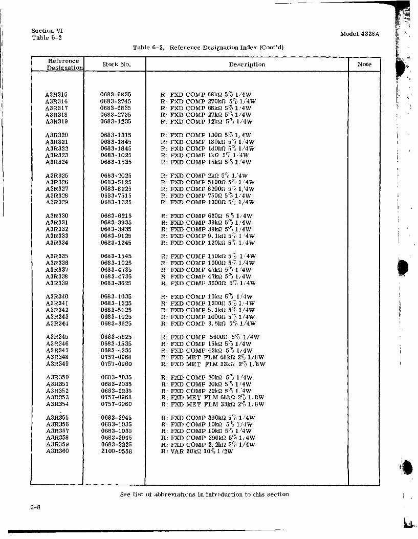
Section VI Table 6-:!
Reference Designation
A3R315 A3R316 A3R317 A3R318 A3R319
A3R320 A3R321 A3R32:! A3R323 A3R324
A3R32S A3R326 A3R3:!7 A3R3:!8 A3R3:!9
A3R330 A3R331 A3R332 A3R333 A3R334
A3R335 A3R336 A3R337 A3R338 A3R339
A3R340 A3R341 A3R342 A3R343 A3R344
A3R345 A3R346 A3R347 A3R348 A3R349
A3R350 A3R351 A3R352 A3R353 A3R354
-
A3R355 A3R356 A3R357 A3R358 A3R359 A3R360
6-8
Model 4328A
Table 6-2, Reference Designation Index (Cont'd)
Stock No. Description Note
0683-6835 R FXD COMP 68kO 5L'b 1/4W 0683-2745 R: FXD COMP 270k0 S~ 1/4W 0683-6835 R: FXD COMP 68k0 5L'b 1.'4W 0683-273S R~ FXD COMP 27kO 500 1/4W 0683-1335 R: FXD COMP 12k0 S0:J 1/4W
0683-1315 R: FXD COMP 1300 500 1!4W 0683-1845 R~ FXD COMP 180kO 5t'Q 1/4W 0683-184S R: FXD COMP 180kO 5U0 1/4W 0683-1025 R: FXD COMP 1kr.! 5o;', 1 .'4W 0683-1535 R: FXD COMP 15k0 5''0 1./4W
0683-202S R~ FXD COMP 2k0 S'JQ 1/4W 0683-5125 R: FXD COMP 51000 500 li4W 0683-8225 R: FXD COMP 8200(2 500 1/4W 0683-7S15 R: FXD COMP 750!2 500 1/4W 0683-1325 R: FXD COMP 1300!2 500 1/4W
0683-621S R: FXD COMP 620!2 5''0 1/4W 0683-3935 R: FXD COMP 39kr.! 5L'b 1/4W 0683-393S R: FXD COMP 39kr.! 500 1/4W 0683-9125 R: FXD COMP 9. 1kf.! so;', 1,'4W 0683-1245 R: FXD COMP 120kn so;', 1/4W
0683-154S R: FXD COMP 150kf.! 500 1 /4W 0683-102S R~ FXD COMP 10000 S00 1/4W 0683-473S R· FXD COMP 47kf.! 5~ 1 14W 0683-4735 R FXD COMP 47k&1 500 1/4W 0683-3625 R. FXD COMP 3600!2 S00 1/4W
0683-103S R· FXD COMP 10kn 500 1/4W 0683-132S R· FXD COMP 13000 500 1/4W 0683-512S R~ FXD COMP 5.1k0 5% 1/4W 0683-102S R~ FXD COMP 10000 5% 1/4W 0683-3625 R: FXD COMP 3. BkO 5% 1./4W
0683-562S R: FXD COMP 56000 5% 1/4W 0683-1S3S R~ FXD COMP 15k0 500 1.i4W 0683-4335 R: FXD COMP 43kO 500 1/4W 0757-0968 R: FXD MET FLM 68kr.l 2% 1/8W 0757-0960 R: FXD MET FIM 33kr.l 200 l/8W
0683-2035 R.: FXD COMP 20k0 S% 1/4W 0683-2035 R: FXD COMP :!Okr.l 500 l./4W 0683-2235 R FXD COMP 22kn 5Cj, 1. ·4w 0757-0968 R:: FXD MET FLM 68kr.l 2ll,; 1/BW 0757-0960 R: FXD MET FLM 33kr.l 200 1/8W
0683-3945 R:: FXD COMP 390kr.! 5o;'J 1 /4W 0683-1035 R: FXD COMP 10kr.l 5% 1/4W 0683-1035 R FXD COMP 10kr.! 500 1/4W 0683-3945 R: FXD COMP 390kr.l 5% 114W 0683-2225 R: FXD COMP 2. 2kr.l 500 1/4W 2100-0558 R ~ VAR 20kR 10% 1 i2W
See list of abbreVIations in introduction to this section

Model 4328A
Reference Designation
A3T1-A3T300
A3T301 A3T302
A4
A4R1-A4R100
A4R101* A4R102* A4R103
A4R104 A4R105 A4R106 A4R107 A4R108
A4R109* A4R110" A4R111
~I I
,'
A4R112* A4R113*
A4R114* A4R115* A4R116* A4R117* A4R118*
A4Rll9* A4R120* A4R121* A4R122* A4R123*
A4S1--A4Sl00
A4S101
Table 6-2, Reference Designation Index (Cont'd)
Stock No. Description
NOT ASSIGNED 04328-7030 TRANSFORMER ·OSC 04328-7032 TRANSFORMER·
04328-7024 RANGE SWITCH ASS' Y
NOT ASSIGNED 04328-8606 R:FXD W. W. 0. 5!2 0. 1% 04328-8626 R:FXD W. W. 1. 477Q 0.1% 04328-8627 R:FXD W. W. 4. 94!2 0.1%
0-!328-8628 RFXD W. W. 14. 85!2 0.1% 04328-8629 R:FXDW.W. 49.6r.!0.1% 04328-8630 R:FXD W. W. 148. 8!2 0.1% 04328-8631 R:FXD W. W. 497, 1!2 0.1% 0698-2125 R :FXD MET FLM 1. 492kn 0. 100 1 4W
0698-1466 R FXD MET FLM 5kn 0.1%1 4W 0698-2126 R FXD MET FLM 14.11kS2 0.1% 1, 4W 0698-2042 R.FXD MET FLM 51. 1k!J 0. 1% 1 i4W 04328-8621 R:FXD W. W. 560mS2 1% 04328-8622 R:FXD W. W. 390mS2 1%
04328-8623 R:FXDW.W. 350mf.l 100 04328-8624 R:FXDW.W. 340mf.l 100 04328-8625 R:FXD W. W. 330mS2 1% 0698-3444 R :FXD MET FLM 316!2 100 1/8W 0757-0426 R:FXD MET FLM 1.10kS2 1% 1 •8W
0757-0290 R:FXD MET FLM 6.19kS2 1% 1/8W 0698-3157 R :FXD MET FLM 19. 6kS2 1% 1 i8W 0757-0464 R:FXD MET FLM 90. 9kf.l 1% 1 8W 0698-3455 R:FXD MET FLM 261kf.l 1% 18W 0698-3444 R.: FXD 316!2 1% 1 iSW
NOT ASSIGNED 3100-1173 SWITCH:RANGE ROTARY
See list of abbreviations in introduction to this section
'
Section VI Table 6-2
Note
6-9

Section VI Table 6-2
Reference Designation
A5
A5C1-A5C201
A5C202*
A5T1-A5T302
A5T303
A5XA1 A5XA2 A5XA3
A6
A6BT1-A6BT400
A6BT401 A6BT402 A6BT403 A6BT404
A6C1-A6C400
A6C401 A6C402
A6CR1-A6CR400
A6CR401 A6CR402 A6CR403
A6CR404 A6CR405 A6CR406 A6CR407 A6CR408
A6CR409 A6CR410 A6CR411 A6CR412
6-10
Model 4328A
Table 6-2, Reference Designation Index (Cont'd)
stock No. Description Note
04328-7033 MOTHER BOARD 04328-8708 BOARD BLANK P. C.
'-'1>
NOT ASSIGNED 0160-1550 C: FXD MY 0. 015JIF 10~, 100VDCW
NOT ASSIGNED 04328-7031 TRANSFORMER·
NOT ASSIGNED 1251-1886 CONNECTOR: PRINTED CIRCUIT 15 CONTACTS 1251-1886 CONNECTOR: PRINTED CffiCUIT 15 CONTACTS
04328-7026 POWER SUPPLY: RECHARGEABLE BATTERY OPERATION ONLY 04328-8706 BOARD~ BLANK P. C.
'
NOT ASSIGNED 1420-0274 BATTERY: 6V. 225A-HR HG SLDR-TAB
~. ,~
1420-0274 BATTERY: 6V. 225A-HR HG SLDR-TAB 1420-0274 BATTERY: 6V. 225A-HR HG SLDR-TAB 1420-0274 BATTERY 6V. 225A-HR HG SLDR-TAB
NOT ASSIGNED I 0180-0965 C:: FXD ALUM 220JlF 25VDCW I
I
0180-0965 C· FXD ALUM 220JlF 25VDCW
NOT ASSIGNED 1901-0230 SEMICON DEVICE· DlODE SILICON 181625 600V 350mA 1901-0230 SEMICON DEVICE· DlODE SILICON 181625 600V 350mA 1901-0230 SEMICON DEVICE· DlODE SILICON 1S1625 600V 350mA
1901-0230 SEMICON DEVICE· DIODE SILICON 181625 600V 350mA 1902-3208 SEMICON DEVICE: DIODE BREAKDOWN 15. 4V 5% 400mW 1901-0040 SEMICON DEVICE: DIODE SILICON 1901-0230 SEMICON DEVICE: DIODE SILICON 181625 600V 350mA 1901-0230 SEMICON DEVICE· DIODE SILICON 1S1625 600V 350mA
1901-0230 SEMICON DEVICE: DIODE SILICON 1S1625 600V 350mA 1901-0230 SEMICON DEVICE: DIODE SILICON 1S1625 600V 350mA 1902-3208 SEMICON DEVICE: DIODE BREAKDOWN 15 .. 4V 5"0 400mW 1901-0040 SEMICON DEVICE: DIODE SILICON
I
f See list of abbreviations in introduction to this section l
L

Model4328A
Reference Des tgnation
1,,,
A6R1-A6R400
A6R401 A6R402 A6R403
C1 C2 C3-C200 C201 C202-C307
C308
DSl
Fl
J1 J2 J3 J4
J5
Ml
Rl R2 R3
S1 S2 S3
Table 6-2, Reference Designation [ndex (Cont'd)
Stock No. Description
NOT ASSIGNED 0683-6215 R:FXD COMP 620Q 5% 1/4W 0683-6215 R:RXD COMP 620r2 5% 1/4W 0683-3335 R:FXD COMP 33kr2 5% 1 4W
MISCELLANEOUS
5040-0615 HOLDER:BATTERY 2 REQ'D
0160-1235 C: FXD MY 0. 011J-F 1 O% 600VDC W 0180-0934 C:FXD TANT lOO!J-F 2000 10VDCW
-, NOT ASSlGNED 0160-1561 C:FXD MET PAPER 4!1F 10% 150VDCW
NOT ASS lG NED
0160-1562 C:FXD MET PAPER 40/1-F 10% 150VDCW
1450-0566 LAMP:INDICATOR
2110-0110 FUSE:CARTRIDGE 0. IA SLOW-BLOW
1251-2357 CONNECTOR:PO\\ER 3 PIN MALE 04260-5028 CONNECTOR:FOR RECORDER 04260-5028 CONNECTOR:FOR GROUND
CONNECTOR:PROBE NOT SEPARATELY REPLACEABLE PART OF W2 PROBE CABLE ASS'Y.
1250-0318 CONNECTOR:FOR PROBE
1120-0751 METER
0757-0476 R:FXD MET FLM 30lkr2 I% 1/8W 0683-4725 R:FXD COMP 4. 7kr2 5% 1/4W 0683-4735 R:FXD COMP 47kr2 5% .25w
3101-0033 SWITCH::SLIDE DPDT FOR l15/230 3101-0272 SWITCH:TOGGLE ON-OFF-ON 3101-0273 SWITCH:PUSH BUTTON BATT TEST 3101-0274 KNOB:FOR S2 3101-0275 BRACKET FOR S2
See list of abbreviations in introduction to this section
Section VI Table 6-2
Note
6-11

Section VI Table 6-2
Reference Desig:nation
T1 T2-T2UO T201 T202
W1
W2
XA1
XF1
W4
6-12
Table 6-2, Reference Designation Index: (Cont'd)
Stock No. Description
9100-0735 TRANSFORMER: POWER NOT ASSIGNED
04328-7029 TRANSFORMER: INPUT 04328-7028 TRANSFORMER: INPUT
8120-1378 CABLE ASS'Y:: POWER 1251-0048 ADAPTER: THREE-PRONG TO TWO-PRONG
04328-7203 CABLE ASS'Y PROBE 04328-7202 CABLE ASS'Y
1251-0135 CONNECTOR:PRINTED CKT:5 CONTACTS.
1400-0084 HOLDER: FUSE
16143A PROBE CABLE
PROBE ASSEMBLIES 16005A PROBE: CLIP TYPE, TWO FURNISHED 16006A PROBE: PIN TYPE, TWO FURNISHED 16007A TEST LEAD: ALLIGATOR CLIP RED 16007B TEST LEAD: ALLIGATOR CLIP BLACK
MISCELLANEOUS 0370-0254 KNOB: SKIRTED BAR 03.- 4" BLK.
-
See list of abbreviations in introduction to this section
Model 4328A
Note
1,\
I L

Model 4328A
SECTION VII MANUAL CHANGES AND OPTIONS
Section Vll Paragraphs 7-1 to 7-8
7-1. OPTIONS Table 7-L Backdatmg Changes,
7-2 Options are standard modifications performed on -hp- instruments at the factory, Model 4328A Option 001 rechargeable battery operation is available
7-3. SPEClAL INSTRUMENTS
7-4. "Specials" are standard -hp- instruments that are modified according to customer specifications, A separate insert sheet is included with the manual for special instruments having electrical changes, Make the changes specified in addttion to any other changes that are necessary.
7-5. MANUAL CHANGES
7-6. This manual applies directly to the Model 4328A with serials 1828J057ll and above. The following paragraphs explain how to adapt this manual to apply to later mstruments w1th higher serial prefix, or earlier instruments With lower senal prefLx or number. Technical corrections to this manual (if any) are called errata and are listed on a separate "Manual Changes" sheet supplied with thts manual.
7-7. LATER INSTRUMENTS; If the serial prefix of your Model 4328A is above 1828, refer to a separate "Manual Changes" sheet supplied with this manual. Locate the serial prefb: of your instrument and make the indicated ehanges.
7 -8 .. EAR LlER INSTRUMENTS (Backdating Changes): lf the serial prefb: or number of your Model 4328A is 1828J057l0 and below, refer to Table 7-1 for the changes necessary to adapt this manual to your particular instrument. Locate the serial prefLx or number of your instrument in the table and make the indicated changes. Note that instrument-component values that differ from those in this manual, yet are not listed in this backdating changes, should be replaced usmg the part number given in this manual
Instrument Serial Prefix or Number
723 724-00050 to -00120
723 '724-00121 to -00210
747 748-00211 to -00270
810 811-00271 to -00300
813, 814-00301 to -00341
818 819-00342 to -00440
818 •'819-00441 to -00730
1039 1040 and below
1210 and below
1233 and below
1334-02811 and below
1420 and below
1542J04620 and below
1542J04870 and below
1542J05050 and below
1828J05530 and below
1828J06420 and below
Make Changes
1, 2, 3, 4, 5, 6, 7, 8, 9, 10, 11,12, 13, 14, 15, 16, 17, 18,19,20
2, 3, 4, 5, 6, 7, 8, 9, 10, 11, 12, 13, 14, 15, 16, 17, 18,19,20
3, 4, 5, 6, 7, 8, 9, 10, 11, 12, 13, 14, 15, 16, 17, 18, 19,20
5, 6, 7, 8, 9, 10, 11, 12, 13, 14, 15, 16, 17, 18, 19, 20
6, 7, 8, 9, 10,11,12,13, 14, 15, 16, 17,18, 19,20
8, 9, 10, 11, 12, 13, 14, 15,16,17,18, 19,20
9, 10, 11,12, 13,14, 15, 16,17,18,19,20
10, 11, 12,13, 14, 15, 16, 17, 18, 19, 20
11, 12, 13, 14,15, 16, 17,, 18,19,20
12,13,14,15,16,17, 18, 19,20
13, 14,15, 16, 17, 18, 19, 20
14, 15,16,17, 18,19,20
15, 16,17, 18,19,20
16, 17, 18, 19,20
17, 18, 19, 20
18, 19, 20
20
7-1

I'· I I
'
Section VII Model 4328A
7-2
CHANGE 1
Page 6-4, Table 6-2 Add A2CR205, HP Part No. 1901-0040, DIODE:SILICON. Change A2R201 and A2R207 to HP Part No~ 0683-1545, R·FXD COMP 150k.Q 5'i1 1 • 4W. Change A2R202 and A2R208 to HP Part No. 0683-1045, R.:FXD COMP 100k.Q 5% 1. 4W.
Page 6-5, Table 6-2 Delete A2R238. Change A2R201 and A2R207 to 150k.Q. Change A2R202 and A2R208 to 100k.Q.
Page 8-19, Figure 8-18
PHASE- SENSITIVE AMPUFIER ASS"Y I 04328-70221
Replace A2R238 with A2CR205 as shown in partial schematic Figure 7-1.
~ IJ208
R232 LIN ~J
R234
---) C21Z CR2 c 20~
Ff224
Figure 7-1. Partial Schematic of A2 Ass'y
CHANGE 2
Page 6-6, Table 6-2 Change A3 Board Ass'y, HP Part No. 04328-7034 to 04328-7023.
Service Note Board Ass'y 04328-7023 is interchangeable with Board Ass'y 04328-7043 ..
Page 6-7, Table 6-2 Delete A3CR32 1.
Page 6-8, Table 6-2 Change A3R342 to HP Part No .. 0683-3325, R:FXD COMP 3 3kr.l 5% 1/4W .. Change A3R344 to HP Part No .. 0683-4325, R:FXD COMP 4 3kr.J 5% 1 4W. Change A3R346 to HP Part No .. 0683-1045, RFXD COMP lOOkQ 5% 1i4W.
Page 8-17, Figure 8-14 Change a part of A3 schematic as follows
--------
R341
CR313
R34T
Figure 7-2. Partial Schematic of A3 Ass'y
Page 6-11, Table 6-2 Delete C2 IOO!J-F connected between Recorder output terminals ..
Page 8-19, Figure 8-18 Delete C2, 100{.lF capaCitor.
~·
L '
'

~ ..
Model 4328A
CHANGE 3
Page 6-9, Table 6-2 Change A4R112 to HP Part No .. 04328-8618, R.:FXD W. W. 750mS"2 0. 200 .. Change A4Rll3 to HP Part No .. 04328-8617, R:FXD W. W. 490mS"2 0. 2%. Change A4R114 to HP Part No .. 04328-8616, RFXD W. W. 430mS1 0. 2% .. Change A4Rl15 to HP Part No .. 04328-8615, R:FXD W. W. 414mS"2 0. 200 .. Change A4Rl16 to HP Part No .. 04328-8614, R:FXD W. W. 406mS"2 0. 200 ..
Service Note; These five resistors mentioned above are not separately replaceable. [f necessary, replace all five resistors as a set to the values shown in this manual.
Page 8-17, Figure 8-14 Change A4Rl12 to 750mS"2, A4Rl13 to 490mS"2, A4Rl14 to 430mS"2, A4R115 to 414mn and A4R116 to 406mS"2 ..
CHANGE 4
Page 6-6, Table 6-2 Change A3C318 to HP Part No .. 0180-1029, C:.FXD TANT 1p_F 20o;:, 15VDCW
Page 6-7, Table 6-2 Change A3R303 to HP Part No .. 0683-3945, R:FXD COMP 390kS1 500 1 4W .. Change A3R304 to HP Part No 0683-3935, R:FXD COMP 39kS"2 500 1/4W Change A3R305 to HP Part No 0683-1035, R:FXD COMP lOks-2 5% V4W. Change A3R310 to HP Part No 0683-1535, R:FXD COMP 15kS1 5% 1/4W. Change A3R311 to HP Part No 0683-5125, R:FXD COMP 5 .. lks-2 500 t/4W. Change A3R313 to HP Part No 0683-6835, RFXD COMP 68kS"2 500 1. 4W Change A3R314 to HP Part No .. 0683-1235, R:FXD COMP 12kS"2 500 1 ~'4W.
Page 6-8, Table 6-2 Change A3R323 to HP Part No .. 0683-3325, R·FXD COMP 3 .. 3kS1 500 1/4W
Page 8-17, Figure 8-14 ,_ Change A3R303 to 390kS"2, A3R304 to 39kr2, A3R305 to 10kr2, A3R310 to 15kr2, A3R31L to 5 .. 1kr2, A3R313 to 68kr2, A3R314 to 12kS'2 and A3R323 to 3. 3kr2.
CHANGE 5
Page 6-4, Table 6-2 Change A2C207 to HP Part No 0140-0194, C:FXD MlCA llOpF 500 300VDCW.
Service Note- See "CHANGE 9"
Page 6-5, Table 6-2 Change A2R238 to HP Part No .. 0683-4715, RFXD COMP 470S'2 500 1 4W.
Page 6-6, Table 6-2 Delete A3C322.
Page 8-19, Figure 8-18 Change A2C207 to llOpF and A2R238 to 470S"2 ..
Page 8-17, Figure 8-14 Delete A3C322 ..
CHANGE 6
Page 6-7, Table 6-2 Change A3R304 to HP Part No .. 0683-2035, RFXD COMP 20kr2 5% 1/4W.. Delete A3CR322 and A3CR323.
Page 6-8, Table 6-2 Delete A3R360 ..
Page 8-17, Figure 8-14 Delete A3CR322 and A3CR323 Change A3R304 to 20kr2. Delete A3R360 and replace with a short circuit.
Section VII
7-3

Sectron VIT Model 4328A
CHANGE 7
Page 6-3, Table 6-2 Change A1CR305 and A1CR310 to HP Part No 1902-3110, DIODE:BREAKDOWN 5 .. 9V 2% ..
Service Note: Use 1902-0049 for replacement
Page 8-21, Figure 8-20 Change the statement of A1CR305 and AlCR310 to 5 .. 9V
CHANGE 8
Page 6-5, Table 6-2 Change A2R230 to HP Part No' 0757-0199, R FXD MET FLM 21.. 5k0 100 1, 8W, Change A2R234 to HP Part No. 0698-3155, RFXD MET FLM 4 .. 64k!J 1% 1.'8W
Page 8-19, Figure 8-18 Change A2R230 to 21. 5k!J and A2R234 to 4 64k!J
CHANGE 9
Page 6-4, Table 6-2 Change A2C207 to HP Part No .. 0140-0204, C FXD MICA 47pF 500 300VDCW..
Service Note If the accuracy on the 1000 Range does not meet with specifications when a sample under test has a series reactance up to two times full scale resistance, proceed following adjustments:
1) Adjust A2C208 2) Change A2C207 to a value between 47pF and 91pF. 3) Change A5C202 to a value between 0 .. 020)1F and 0. 024pF
Page 8-19, Figure 8-18 Change A2C207 to 47pF
CHANGE10
Page 6-2, Table 6-2 Change HP Part No. of METER TRIM to 5020-0704. Change HP Part No. of SIDE COVER to 5000-0703. Change HP Part No. of COVER:TOP to 5070-0706, Change HP Part No. of COVER:BOTTOM to 5000-0711. Change HP Part No. of PANEL:REAR to 04328-1022. Change HP Part No. of PANEL:FRONT to 04328-1021.
Page 6-11, Table 6-2 Add A7; 04328-7035, POWER SWITCH ASS'Y. Add A7R1-A7R403; NOT ASSIGNED. Add A7R404; 0757-0476, RFXD MET FLM 301k0 100 1 · 8W. Add A7R405; 0683-4725, R::FXD COMP 4. 7k!J 5o;'1 1'4W. Add A7S1; 3101-0247, SWITCH:POWER PUSH BUTTON UEG-42L. Add A7S2; 3101-0249, SWITCH.:BATT TEST PUSH BUTTON UEG-421.
Delete R1; 0757-0476, R:FXD MET FLM 301k0 1% l8W. Delete R2; 0683-4725, R:FXD COMP 4. 7k0 5% 1."4 W. Delete R3; 0683-3335, R:FXD COMP 33k!J 5% L'4W. Delete S2; 3101-0272, SWITCH:TOGGLE ON-OFF-ON. Delete S3; 3101-0273, SWITCH:PUSH BUTTON BATT TEST. Delete DS1; 2140-0015, IAMP:NEON NE-2H. Add DSl; 1450-0048, LAMP:LIGHT-IND, RED.
Page 6-12, Table 6-2 Change HP Part No. of W1; CABLE ASS'Y:POWER to 8120-0078. Add W3; 04328-7202, CABLE ASS'Y.
7-4 Delete XA1, 1251-0135, CONNECTOR:PRINTED CffiCUIT 15 CONTACTS.
'·'
•,','
II~ -
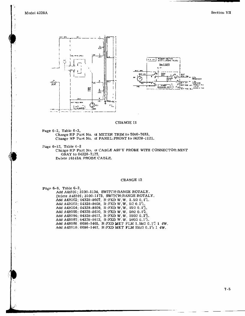
:,,
Mode14328A
WHT I:;RA RED
5I
~r __ , I
~--
WHT REO BAN
CHANGE 11
Page 6-2, Table 6-2, Change HP Part No. of METER TRIM to 5060-7633. Change HP Part No. of PANEL:FRONT to 04328-1121.
Page 6-12, Table 6-2 Change HP Part No. of CABLE ASS'Y PROBE WITH CONNECTOR:MINT
GRAY to 04328-7127. Delete 16143A PROBE CABLE.
CHANGE 12
Page 6-9, Table 6-2, Add A4S101; 3100-1134, SWITCH:RANGE ROTALY. Delete A4S101; 3100-1173, SWITCH:RANGE ROTALY. Add A4R102; 04328-8607, R:FXDW.W. 1.5!2 0.1%. Add A4R103; 04328-8608, R:FXD W. W. 5!1 0.100. Add A4R104; 04328-8609, R :FXD W. W. 15!2 0. 100. Add A4R105; 04328-8610, R:FXD W. W. 50n 0.1%. Add A4R106; 04328-8611, R :FXD W. W. 150!2 0.1 %. Add A4Rl07; 04328-8612, R:FXD W. W. 500!2 0.1%. Add A4R108, 0698-1465, R:FXDMET FLM 1.5kn 0.1%1 4W. Add A4R11 0; 0698-1467, R :FXD MET FLM 15kn 0. 100 1 4W.
Section VII
7-5

Sectwn Vli
7-6
Delete A4R102; 04328-8626, R:FXDW.W. 1.447!2 0.1%. Delete A4R103; 04328-8627, R:FXD W. W. 4. 9451 0.1%. Delete A4R104; 04328-8628, R:FXD W. W. 14.8551 0.1%. Delete A4R1 05; 04328-8629, R :FXD W. W. 49. 651 0. 1%. Delete A4R106; 04328-8630, R:FXDW.W. 148.8510.100. Delete A4R107; 04328-8631, R:FXDW.W. 497.1510.1%. Delete A4R108; 0698-2125, R:FXD MET FLM 1. 492kn 0.1%. Delete A4R110; 0698-2126, R:FXD MET FLM 14.11kn 0.1%_
CHANGE 13
Page 6-5, Table 6-2, Add A2R228, 2100-1777, R:VAR W. W. 20k51 LIN 5% lW. Add A2R229, 2100-1777, R:FAR W. W. 20k51 LIN 5% lW. Add A2R232, 2100-1775, R:VAR W. W. 5k51 LIN 10% L 2W. Add A2R234, 0757-0439, R:FXD MET FLM 6.81k!l 1%1 8W. Add A2R230; 0698-3161, R:FXD MET FLM 38. 3k!l 1% 1 i8W.
Delete A2R228, 2100-1948, R:VAR W. W. 50k!l LIN 5% 1W. Delete A2R229; 2100-1948, R:VAR W.W. 50k!l LIN 500 1W. Delete A2R232; 2100-1777, R:VAR W. W. 20k!l LIN 5% 1W. Delete A2R234; 0757-0283, R:FXD MET FLM 2kR 1% 1 '8W. Delete A2R230; 0757-0959, R:FXD MET FLM 30k!l 2% 1 "8W.
CHANGE 14
Page 6-4, Table 6-2, Delete~A2C218; 0160-0127, C :FXD CER 11lF 20% 25VDCW.
Page 4-7, Figure 4-5, Delete A2C218.
Page 8-19, Figure 8-17, Delete A2C218.
Page 6-7, Table 6-2, Change A3CR322 to HP Part No. 1902-3110, DIODE BREAKDOWN 5. 9V 400mW. Change A3CR323 to HP Part No. 1902-3110, DIODE BREAKDOWN 5. 9V 400mW. Change A3Q312 to HP Part No. 1853-0010, TRANS[STOR :SILICON. Change A3Q313 to HP Part No. 1853-0010, TRANSISTOR :SILICON.
Page 8-17, F1gure 8-14, Change voltages of CR322 and CR323 to 5. 9V.
Page 6-2, Table 6-2, Change HP Part No. of PANEL:FRONT to 04328-1221.
Page 6-11, Table 6-2, Change DS1 to 2140-0015, LAMP :NEON NE-2H.
5040-0234, LAMP :HOLDER FOR DS1. 5040-0235, LAMP :HOLDER FOR DS1.
Change R3 to HP Part No. 0683-3335, R FXD COMP 33kR 5% 1. 4W.
Model 4328A
,, . . ,
1,,,

I ~
Moc'el 4328A
CHANGE 15
Page 6-4, Table 6-2, Page 8-19, F1gure 8-17, Change A2C207 to HP Part No. 0140-0193, C ·FXD MICA 82pF 5% 300VDCW.
CHANGE16
Page 6-4, Table 6-2, Page 8-19, Figure 8-17, Change A2C207 to HP Part No. 0160-2204, C;FXD MICA lOOpF 5% 300VDCW.
CHANGE 17
Page 6-4, Table 6-2, Page 8-19, Figure 8-1, Change A2C207 to HP Part No. 0140-0191, C;FXD MICA 56pF 5% 300VDCW.
CHANGE 18
Page 6-5, Table 6-:l, Change A2R228 to HP Part No. 2100-3253, R:VAR 50k!;l 10% 1/2W. Change A2R229 to HP Part No. 2100-3253, R :V AR 50kn 10% 1. 2W. Change A2R232 to HP Part No. 2100-0558, R :VAR !lOkr.! 10% 1 12W. Change A2R233 to HP Part No. 2100-0567, R:VAR 2kn 10%1 2W.
CHANGEL9
Page 6-4, Table 6-2, Change A2Q209 to HP Part No. 1854-0071.
Page 6-7, Table 6-2, Change .A3Q301 and A3Q308 to HP Part No. 1854-0071.
CHANGE 20
Page 6-5, Table 6-2, Add A2R225; 0683-2035, R: FXD 20kn 5% 1. 4W. Add A2R228; 2100-3253, R: VAR 50kr.! 10% 1/2W. Add A2R229; 2100-3253, R: VAR 50kQ 10% 1/2W. Add A2R230; 0757-0453, R.: FXD 30.1k1"1 1% 1/8W. Add A2R232; 2100-0558, R: VAR 20kQ 10% 1/2W. Add A2R234; 0757-0283, R: FXD 2kn 1% 1/8W.
Delete A2R225; 0698-3160, R: FXD 31.6kr.! 1% 1i8W. Delete A2R228; 2100-0558, R: VAR 20k\2 10% 1 /2W. Delete A2R229; 2100-0558, R: VAR 20kQ 10% 1/2W. Delete A2R230; 0698-3161, R: FXD 38. 3kr.! 1% 1,'8W. Delete A2R232; 2100-3252, R:. VAR 5kr.! 10% 1. 2W. Delete A2R234; 0757-0439, R: FXD 6. 81kn 1% 1.'8W.
Section Vll
7-7

NOTES
Model 4328A Section Vlll Paragraphs 8-1 to 8-13
SECTION VIII
TROUBLESHOOTING AND CIRCUIT DIAGRAMS
8-1. INTRODUCTlON
8 -2.. This section contains troubleshooting instructions, schematics, and component locations [or the milliohmmeter. Also included is an overall block diagram that indicates the location of test point in the instrument
8-3. Reference designations shown within circuit card outlines are abbreviated, To find the part m the Reference Designation Index, use the full reference designation. For example, R305 on the A3 Oscillator Assembly is listed as A3R305.
8-4. The Schematic Diagram Notes in Figure 8-1 pertam to all the schematics. Additional notes on the schematics indicate test conditions, and special information for use when maintain the instrument.
8-5 .. TROUBLESHOOTING
8-6.. Table 8-1 is the Overall Troubleshooting chart for the milliohmmet~r. Procedures for isolating circuit malfunctwns to specific stages are based on the use of the YEW Type 2782 Standard Resistors and YEW Type 2786 or GR Model 1432T Decade Resistance Box and the calibration procedures in Section V. The mformation obtained when calibration is attempted is used to troubleshoot the instrument.
8-7.. Table 8-1 contains references that dtrect the user to the detailed troubleshooting charts, Table 8-2 through 8-10.. The detailed charts refer the user to transistor stages.. [n a few instances, specific parts
are called out as being possible causes of circuit malfunction, however, the troubleshooting charts are not intended to locate specific parts that have failed. They are intended to locate only malfunctioning stages.
8-8. SCHEMATICS
8-9 The schematics contain signal routmginformahon, nominal voltage levels, and notes that assist in understanding the circuit. They are laid out to show electrical operation, and are not intended as wiring diagrams.
8-lO. Component location photographs next to the schematics indicate the physical location of parts. Test pomts are also shown.
8-ll. Factory selected parts are indicated by an asterisk. These are components that generally are installed to fulfill circuit operatwn requirements .. They may be the nominal value, or they may be some value close to nominal. In any case, if the component fails, ctrcuit operation should be verified after these components are replaced ..
8-12. Component values are shown as follows unless otherwise noted.. Resistance in ohms, capacitance in microfarads and inductance in microhenries.
8-13. Wire color is indicated as WHT./ YEL i VIO. First color identifies ground color, second color identifies wide stripe, tlurd color identifies narrow stripe.
8-1

Section VIll Figure 8-1
8-2
r---, L __ J
0 @
Model 4328A
SYMBOLS SWITCH DESIGNATIONS
FRGrH PAtJEL
REAR PAtJEL
KtWB COtHROI- A351BR(2-1 2)
SCREWDRIVER ADJUST
FEEDBACI< PATH AJSl SWITCH 51 WITHIN ASSEMBLr A3
COtmUCTitJG ELEMEtH
WIPER MOVES TOWARD "CW" WHEN COtJTROL IS ROTA TED CLOCKWISE
POWER LltJE GROUtW
CIRCUIT COMMm< GROUtW
TEST POitH
"AND" GATE
INHIBIT GATE
"OR" GATE
WA liE FORMS SHOWN ARE T iPICAL
B
R
( 2-1 2)
REFERENCE DESIGNATIONS
2tm WAFER FROM FROtH IA=1ST, ETC)
REAR OF WAFER iF=FRONT)
TERMI~JAL LOCATIOn l2j-) !VIEWED FROM FRONT)
REFEREtKE DESIGNATIONS WITHitj ASSEMBLIES ARE ABBREVIATED ADD ASSEMBLY NUMBER TO ABBREIIIATIIJtJ FOR COMPLETE DESCRIPTION
A'35EMBL~ ABBREVIATIOtJ COMPLETE DESCFIIPTIOt<
A25 Cl A25C1 A25A1 CRl A25A1CRI
no PREFI>< J3 J3
Frgure 8-1 Schematic Diagram Notes
I J not mounrt d
+6 3V TO
A5PI(6)
\ +6 H _uprfl ui
lrom IJ lo Pm 6 0, P.f oiM
4 .stmbJi -t5
t,•
''IL

Model 4328A
TEST POINT MEASUREMENT CONDITIONS AND LOCATIONS
Measurement Conditions
1. Set Range Switch to lmn.
2.. DC voltage check, probes open and shorted (voltage in both conditions shown in schematics).
3.. To observe waveforms, connect a p1ece of copper wire (AWG #12 - #18) across probes, and adjust the length to get full scale deflection.
4. Measurement made with respect to CIRCUIT COMMON.
Waveform Test Point Locations
Test Pgint Location ~
A3TPl A3Q303 EMITTER
A3TP2 A3Q307 BASE
A3TP3 A3Q316 BASE
A3TP4 A3 BLU
A3TP5 A3 (9, K)
A3TP6 A3Q312 BASE
A2TP7 A2Q201 BASE
A2TP8 A2Q202 BASE
A2TP9 A2Q204 BASE
A2TP10 A2Q205 COLLECTOR
A2TP11 A2 CR202, CR203 junction
A2TP12 A2 (2, B)
A2TP13 A2 (3, C)
A2TP14 A2 (8), (11) Use Differential Input.
A2TP15 A2Q209 EMITTER
~scLLAT I 4328-7(
[
[
I ______ -
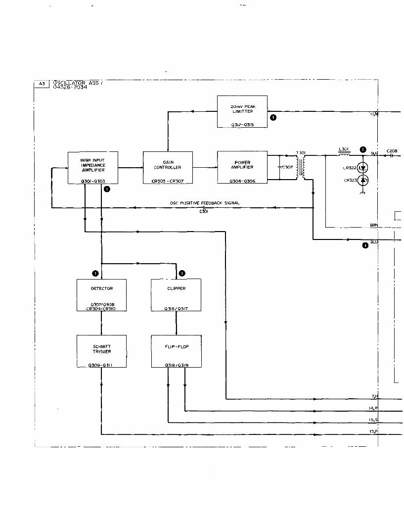
~SC-ILLATOR ASS ( -----------------
1 4328-7034
L ___ _
HIGH INPUT IMPEDANCE AMPLIFIER
0301-0303
0
• DETECTOR
Q307/Q308 CR309/CR310
SCHMITT TRIGGER
0309-0311
GAIN CONTROLLER
CR303 -CR307
20mV PEAK LIMITTER
Q312-Q315
POWER AMPLIFIER
Q304-Q306
OSC POSITIVE FEEDBACK SIGNAL
C301
• CLIPPER
Q316/Q317
FLIP-FLOP
Q318/Q319
•
C307 II "--
BRN
.BL~
I
7,~
14,R
15,5
~---1
F
I
'
L

---------, '
11,1'< C201
J ~
043 28-7022 -' -- ' 0 ' T303 '0 L301
914 C208 r
115 s CURRENT TIP T201
-
-
CR322~ ~ VOLTAGE TIP
II AC 0 • PHA
R> !f202 A~PLIFIER DETEC
- CR323~ ~ • R I CURRENT TIP Q 01-0205 CR202/ I
l VOLTAGE TIP
' J'i L __ ~ ' 0 H-~-l -"" -PRANG~ SWITCH ASS'Y
- -
RMO~ T202 I 0432 -7024 ,....= I
BRN • __ j I r----11 I r-() I I 8
~------------- I
0 BLI ' / 5101 I I I
I ,.
' I RIOI ~
~ l M<louLATOR RI02 Rll2
! I v I
3
0209 - RI03 Rll3 - ~ v I
I mn ' i G) ' RI04 Rll4
ru I
91< - - 3 c --. RICI5 Rll5
~ -.,
'
I I RI06 Rll6
300
I - RI07 ~
i:ij I ' I ' I
- RIOB >-{)
I I
I ' RI09 >-{) ~ n I
I - RIIO ~ ~I I
I
' Rill
100 - _j I
- Lo
-- -- - -' I
7,~ I KHz LEVEL COMPENSATION SIGNAL
! 14,R I
1'3,51 1KHz PHASE REFERENCE SIGNAL
OVER RANGE SIGNAL
. OT.J ,ORAJDACI- TT3JW

I A2l PHAk_E_S_E_N_S_IT_I_V_E AMPLIFIER ASS'Y [-----J 043l:38 - 7022
10 _IA,L~---~-------.
AC 0 A~PLIFIER
~ 0 01-0205 ' L-~~~~~~--~
L 14H, Po ---u~ --l
T202 I= I
I ____ IT~- __ j
11~8
' I
,JDULATOR
I
• PHASE
DETECTOR
CR202/CR203
' I
I DC AMPLIFIER 10,1 0206/0208 I
I
I
I
I
0209 _j' I._· ------ ~9hli.K'----- - - ---=3"-'~"--1-- - -1-2~~_,_8 -- - - --- 1-'Lo-- -
I I
Section VIII Figure 8-2
Ml
/ )
RE CORDER "-,ou fPUT
Figure 8-2. Overall Block Diagram
8-3
.Q
.c
~(
ir
a Q;
n
L
Q
Q IQ
I l
I (
IQ
~Q
~Q
~Q
~Q
2 (
2 I
21
21
2Q
'
SEE INSIDE
·.
Figure 8-2
OVERALL BLOCK DIAGRAM
8-3

Section VIII Figure 8-3
50mV/cm lms/cm
0. 5V/cm lms/cm
lOmV/cm lms/cm
500tN/cm 1ms/cm
500tN/cm lms/cm
8-4
0
0
0
•
0
lOmV/cm lms/cm
2V/cm Lms/cm
2V/cm
5V/cm 0. 5ms/cm
5V/cm
100J1V/cm lms/cm
500/.lV/cm lms/cm
Figure 8-3. Model 4328A Waveforms
Model 4328A
0
• •

,, ,'
!!'','
I t ,,
Model 4328A
0
TABLE 8-1 4328A OVERALL TROUBLESHO<
CHECK CAL£BRATlON USE YEW TYPE 2782 AND YEW TYPE 2786 OR GR MODEL 1432T
-oK-
MET I ~--CALL
I----NOD
MET I ----- oo E1
PROE
TABLE 8-1 4328A OVERALL TROUBLESHOOTING
CHECK CALIBRATION USE YEW TYPE 2782 AND YEW TYPE 2786 OR GR MODEL 1432T
CHECK lliSTRUMENT
-OK---- ELECTRICAL L. OK- FUNCTIONS BAD-ZERO PROPERLY
CHECK AND BAD - ADJUST A2R228
WON'T CALIBRATE 1--------OK--------- CHECK WAVEFORMS ----1
METER DEFLECTS,_ RECALIBRATE CALIBRATION BAD
CHECK FUSE, BATTERY
1--- NO DEFLECTION- POWER SUPPLY---t (+13V, -13V NOMINALLY)
A3T.P .. 4, 5
A30 0
CHECK BAD-POWER SUPPLY
TABLE 8-9 OR 8-10
OK
CHI A2 ~
A2
OK
CHECKWAVEFORMS_L OK-A3 T P 4, 5 BAD•
METER GOES TO CHECK FOR ....._ ___ EVEN IF -OPEN PROBES--~
PROBES SHORTED (AND T302)
A30 0
REPAIR OR BAD- REPLACE
PROBE (AND T302)
CHECK WAVEFORMS OK- A3 T P 4, 5
A30 0
OK-
BAD·
K
CHECK BAD- OSCILLATOR
TABLE 8-2 TO 8-5
CHECK WAVEFORM A2 T P 7
A2 8
L CHECKFOR OPEN PROBES (AND T302)
BAD- CHECK OSCILLATOR TABLE 8-2 TO 8-5
CHECK PHASE SENSITIVE
OK- AMPLIFIER TABLE 8-6 TO 8-8
CHECK POWER
BAD-SUPPLY VOLTAGE (+13V, -13V NOMINALLY)
CHECK BAD-MOTHER
BOARD
CHECK WAVEFORM
OK- A2 T P, 9
A2 0
CHECK OK- OSCILLATOR
TABLE 8-2 TO 8-5
CHECK POWER
BAD- SUPPLY TABLE 8-9 OR 8-10
CHECK WAVEFORM A2 T. P 8
BAD-A2 0 AND MODULATOR TABLE 8-8
CHECK WAVEFORMS ~ OK- A2 T .. P 12, 13
A2 CD 8
CHECK WAVEFORM
OK-A2 T, P 14 -
A2 4D
CHECK FLIP-FLOP
BAD-TABLE 8-4 AND PHASE DETECTOR AN DC AMPLIFIEF TABLE 8-7
NOTES-
TEST INSTRUMENTS REQUIF OSCILLOSCOPE VOLTMETER (SEE TABLE 5-1)
INSTRUMENT TEST CONDIT! SET RANGE SWITCH TO 1rr DC VOLTAGE CHECK, PROBES OPEN AND SHORT (VOLTAGES IN BOTH CONDITIONS SHOWN IN SCI TO OBSERVE WAVEFORMS CONNECT A PIECE OF COl (AWG #12- #18) ACROSS Pl AND ADJUST THE LENGTH GET FULL SCALE DEFLE(

CHECK WAVEFORM
>K-A2 T.P 14
A2 G)
CHECK FLIP-FLOP
3AD-TABLE 8-4
'ES:
AND PHASE DETECTOR AND DC AMPLIFIER TABLE 8-7
INSTRUMENTS REQUIRED ILLOSCOPE ,TMETER ~TABLE 5-1)
lUMENT TEST CONDITIONS RANGE SWITCH TO lmr.l.
VOLTAGE CHECK, )BES OPEN AND SHORTED LTAGES IN BOTH
CHECK
Section VIII Table 8-1
RETURN TO OK- BEGINNING
AND RECHECK
BAD-REPLACE METER
DC AMPLIFIER BAD- AND MODULATOR
TABLE 8-7 AND 8-8
IDITIONS SHOWN IN SCHEMATICS). OBSERVE WAVEFORMS, rNECT A PIECE OF COPPER WIRE G #12 - #18) ACROSS PROBES. > ADJUST THE LENGTH TO ' FULL SCALE DEFLECTION
Table 8-1. Overall Troubleshooting
8-5

,, '·'
SEE INSIDE
Table 8-1
OVERALL TROUBLESHOOTING
8-5
Sect Figu
8-6
Section VIII Figures 8-5 and 8-6
AI ASS'Y T302 T301
@ --~ .J> ·:1 ~
• :t ~ .lJI - ·~ •
li 1 @@ '' c,
·~ ~ ., ,, ,, I -:J , ' I
t t ~ 1) ~ ' I· r,
A3 ASS'Y R306 R360 OSC LEVEL ADJ OSC BIAS ADJ
Figure 8-5. Model 4328A Left Internal View
C201 C308
Figure 8-6. Model 4328A Bottom Internal View
8-6
Model 4328A
J3
' ., '
Jl
J5

Model 4328A
---=-~
TABLE 8-2 OTING OSCILLATOR P/0 A3 JROUBLESHO
NO OSCILLATION (METER GOES TO - EVEN IF PROBES
SHORTED
* CHECK THIS ITEM FIRST
RETURN TO OK - BEGINNING
AND RECHECK
• CHECK W2-04328-707:l PROBE CABLE ASS'Y
CHECK R360 AND CR302 FOR OPEN
CHECK WAVEFORM
REPAIR OR BAD- REPLACE
CHECK C322 CHECK C302, FOR OPEN ---- OK - C304 FOR
OK - BY BRIDGING OPEN SUBSTITUTES
REPLACE BAD-FAULTY
COMPONENT
REMOVE CR322, CR323
BAD-CHECK AND REPLACE
REPLACE BAD- FAULTY
COMPONEN1
A3T.P. 5 --'"'1 OK-
A30 CHECK T301, T302 T201.
OK- CHECK VOLTAGE AT Q306 COLLECTOR
BAD

RETURN TO OK - BEGINNING
AND RECHECK
ECK C302, 14 FOR EN
REPLACE BAD- FAULTY
COMPONENTS ~PLACE
WLTY )MPONENT
CHECK DC LEVEL OF
OK - Q30l, Q302, Q303, Q304
CHECK AND BAD REPLACE
-FAULTY COMPONENTS
CHECK ALL SOLDER
OK- CONNECTIONS ON OSCILLATOR CIRCUIT
FIND AND REPLACE
BAD -FAULTY COMPONENTS
CHECK C301, C322 FOR
OK- OPEN BY BRIDGING SUBSTITUTES
FIND AND FIX
BAD-POOR CONTACTS
TABLE 8-3 SCHMITT TRIGGER P/
CHECK WAVEFORM A3 T. P. 2
A3 0 SAME AS A3 T. P 1
-

iER P/0 A3 TROUBLESHOOTING
tM
CHECK FOR RETU.IDf TO BAD- OPEN CONNECTION OK- BEGINN1NG
IF OSCILLATOR 1 AND REtHECK IS OK •
BAD _ FIND ;ND FIX I
CHECK DC LEVEL AND Q308 INPUT
OK- VIA C310, CR309, CR310
I
CHECK~308 ANDQ3 9 ---1
OK - OUTPU S DC LEVELl
I
!
I
TRAC~ FAULTY BAD- COMP NENT
AND R PLACE
I I
CHECK Q310 OK-ANDQ311
FIND AND BAD -REPLACE
FAULTY COMPONENTS
NOTE:
OK-CHECK CR311
REPLACE BAD- FAULTY
COMPONEN'
DURING NORMAL OPERATION, SCHMITT Til MAY BE CHECKED BY OPENING MOMENTA! LEADS AND MONITORING THE OUTPUT AT
Table 8-2, 8-3,
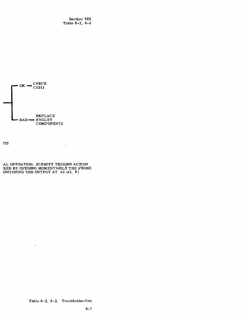
fTS
OK CHECK -CR311
REPLACE BAD- FAULTY
COMPONENTS
Section VIII Table 8-2, 8-3
AL OPERATION, SCHMITT TRIGGER ACTION KED BY OPENING MOMENTARILY THE PROBE ONITORING THE OUTPUT AT A3 (13, P)
Table 8-2, 8-3. Troubleshooting
8-7

L
TABLE OSCILL
NO OSCI (METER - EVE
SHORTE
*C. F
KE INSIO~
Table 8-2, 8-3
TROUBLESHOOTING
8-7

Section VIIT Figure 8-7
8-8
J2
J3
Model 4328A
Tl
Sl CP - -- I
SELECTOR
Fl Jl
Figure 8-7. Model 4328A Rear Internal View
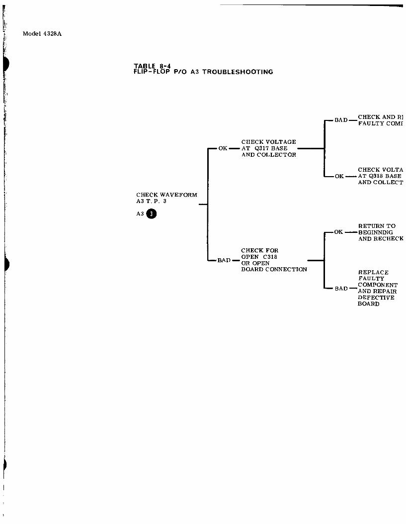
,, ,I
~ Model 4328A '1,1
TABLE 8:-4 FLIP-FLOP P/0 A3 TROUBLESHOOTING
CHECK WAVEFORM A3 T. P. 3
CHECK VOLTAGE OK-AT Q317 BASE
AND COLLECTOR
CHECK FOR BAD OPEN C318
-OR OPEN BOARD CONNECTION
BAD_ CHECK AND Rl FAULTY COMI
CHECK VOLTA OK-AT Q318 BASE
AND COLLECT
RETURN TO OK -BEGINNING
AND RECHECK
REPLACE FAULTY COMPONENT
BAD-AND REPAIR DEFECTIVE BOARD

>REPLACE >MPONENT
.TAGE SE :CTOR
:cK
T ~
CHECK AND BAD-REPLACE
FAULTY COMPONENT
CHECK VOLTAGE OK-AT Q319 BASE
AND COLLECTOR
OK-CHECK CR317, CR319, CR320
CHECK AND REPLACE BAD-FAULTY
COMPONENT
TABLE 8-5 LIMITTER PI'O A3 TRO
CHECK WAVEFORM AND DC LEVEL A3 T P 6

TROUBLESHOOTING
OK - CHECK DC LEVEL OF Q313
CHECK AND REPLACE
BAD- FAULTY I
COMPONENTS
I i
CHECK Q316, OK- CR314, CR315
' i
RETURN TO OK- BEGINNING
AND RECHECK
REPLACE BAD- FAULTY
COMPONENTS
CHECK VOLTAGES OK- AT Q314, Q315
COLLECTOR
REPLACE BAD-FAULTY
COMPONENTS
Tat
CHECK R346, F OK-AND PC BOARI
CONNECTION '1 CR303 - CR307
BAD-CHECK POWER CR313, CR321
Table 8-4, 8-5 Troub

ES
Section VITI Table 8-4, 8-5
CHECK R346, R347 AND PC BOARD
OK-CONNECTION TO CR303 - CR307
BAD_ CHECK POWER SUPPLIES CR313, CR321
Table 8-4, 8-5.. Troubleshooting
8-9

Sf£ INSIDE
Table 8-4, 8-5
TROUBLESHOOTING
8-9

Section VIII Figure 8-8 and 8-9
8-10
f
~' '
t!' I \ ,, r, ,, I
t,
T201
•
A5ASS'Y
R233 A2 ASS'Y REC OUTPUT ADJ
AI ASS'Y
R232 LIN ADJ
-u -r::-
""' ,_
R228 ZERO ADJ
C208 lmn PHASE ADJ
Figure 8-8. Model 4328A Right Internal View
T303 XAI
Figure 8-9. Model 4328A Top lnternal View
@
l '~
q !(
'\!.- • 11 .. tf ~ -@) @
if !"' ·-if --!I !""' -
Model 4328A
,,,

Model 4328A
,,,
,,
'1.
TABLE 8-6 AC AMPLIFIER P/0 A2 TROUBLESHOOTING
CHECK WAVEFORM A2 T. P 7
TABLE 8-7
CHECK DC LEVELS OK- OF Q202, Q203, ---1
Q204
CHECK CONNECTOR BAD A3 (9, K), C308,
-T303, C201, T201, C202
CHECK WAVEFORM A2T.P.10
OK-A28
AND DC LEVEL OF Q205
REPLACE BAD-FAULTY
COMPONENTS
PHASE DETECTOR AND DC AMPLIFIER P/0 A2 TROUBLESHOOTING
CHECK WAVEFORM A2 T. P. 10
BAD-RETURN TO TABLE 8-6
CHECK WAVEFORM OK- A2, T. P 11
A2.
CHECK WAVEFORMS OK-A2T P. 12, 13
A2• 8
CHECK C210 BAD- AND CONNECTION

TABLE 8-8 MODULATOR P/0 A2 TROUBLESHOOTING
CHECK WAVEFORMS A2 T .. P 7, 8
A2e o
CHECK BAD- FLIP-FLOP
TABLE 8-4
MODULATOR OK -FUNCTIONS
PROPERLY
CHECK
FIND BAD-AND
FIX
BAD- CONNECTOR, ---1 T202
CHECK BAD-CR202,
CR203
CHECK OK DC LEVELS
-oF Q201, Q202, Q203
RETURN TO OK- BEGrNNING
AND RECHECK
REPLACE BAD-FAULTY
COMPONENT
CHECK WAVEFOR
OK-A2 T.P 1:
A2-
REPLACE BAD-FAULTY
COMPONE

CHECK WAVEFORM
-A2 T P 11
A2-
REPLACE )-FAULTY
COMPONENTS
CHECK WAVEFORMS A2 T .. P 12, 13
OK-
A2 e 8
BAD-CHECK FAULTY COMPONENTS
I CHECK QK _ Q206A/B, ---1
1 Q208 DC i LEVELS
I
I CHECK
1 CONNECTOR FIND AND
AD-REPLACE FAULTY
i COMPONENT
CHECK AND REPLACE
BAD-FAULTY COMPONENT
CHECK Q209-DC LEVELS CHECK
OK-WAVEFORM A2 T. P. 15
A2 G)
T
BAI
OK
Tables 8-6 through 8

'HECK AND lEPLACE 'AULTY ~OMPONENT
~HECK Q209 ->C LEVELS :HECK VAVEFORM ~2 T. P. 15
Section VIll Tables 8-6 through 8-8
CHECK AND BAD _REPLACE
FAULTY COMPONENTS
OK CHECK METER -ANDS2
Tables 8-6 through 8-8. Troubleshooting
8-11

TABLE AC AM
CHECK A2 T. P.
A28
TABLE PHASE
CHECK A2 T. P
A28
SEE IMSIOE
Table 8-6 through 8 -8
TROUBLESHOOTING
8- 11
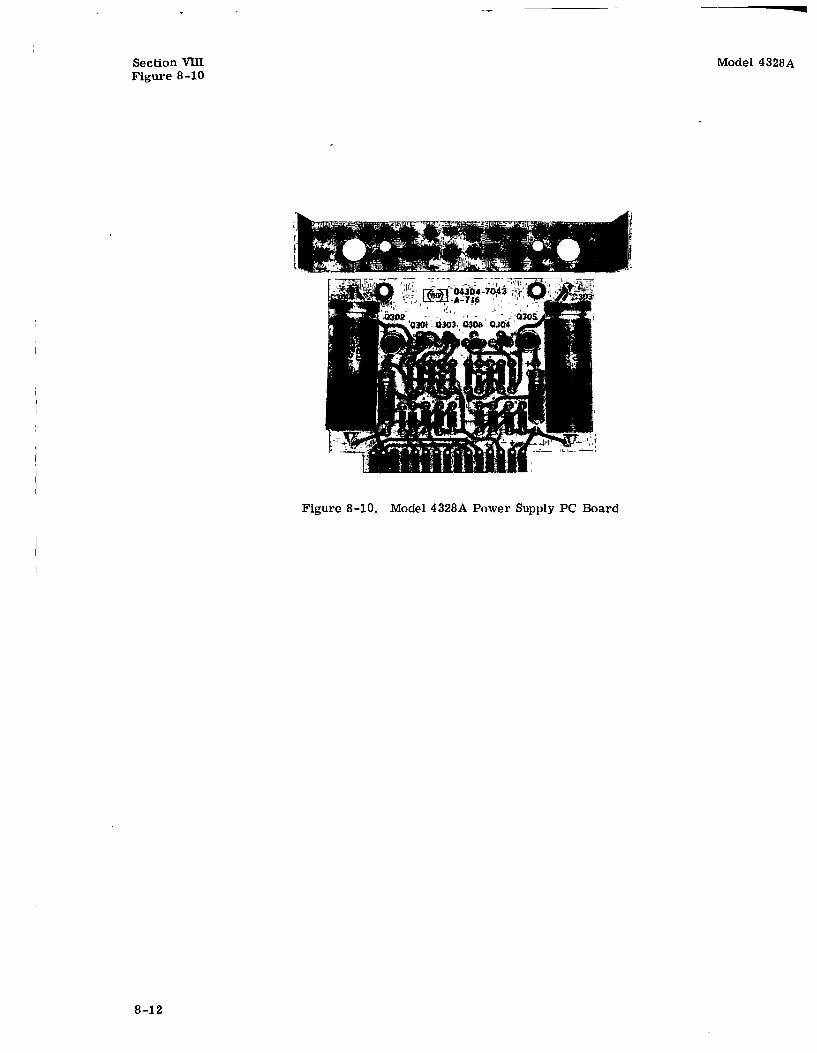
Section VIll Figure 8-10
8-12
Model 4328A
Figure 8-10. Model 4328A Power Supply PC Board

Model 4328A
TABLE 8-9 POWER SUPPLY TROUBLESHOOTING
>(
~22V
MEASURE ±13V SUPPLY MOTHER BOARD (WHT/RED, WHT)
< 12V MEASURE VOLTAGE ACROSS C301
12V TO 14V CHECK -+--REGULATION- CR305,
BAD R302
MEASURE VOLTAGE AT Q302 COLLECTOR
> 14V
MEASURE VOLTAGE ACROSS CR305 -
<(
CHECK FUSE, TRANSFORMER, C301, CR301 -
OV CR304
CHECK OK-Q301, Q302,
Q303
REPLACE BAD-FAULTY
COMPONEN
IF READING IS SAME, CHECK AND REPLACE FAULTY Q302
IF SLIGHTLY DIFFEREN'I BUT HIGH, CHECK CR305, R302, R303, R304

NO SHORT-----------------------------------------------------------------
> 0. 5V OVER LOAD
1\GE
< 05V
!:CK 1, Q302, 3
:PLACE ,ULTY IMPONENTS
AME, 'LACE
~FE RENT :K 03, R304
CHECK FOR SHORTED SUPPLY
SHORT _ FlND AND FIX
REMOVE SUPPLY REPLACE
CR305 1 WORK - CR305
PUT CR305 SUPPLY BACK lN DON'T -CIRCUIT
OK- MEASURE VOLTAGE AT Q301 EMITTER
CHE BAD-REP
Q301
WORK MEASURE VOLTAGE AT Q303 COLLECTOR
MEASI OK- AT Q3'
CHECK AND BAD -REPLACE R301
Q303
NOTE: SAME FORMAT AS DESCRIBED ABOVE CAN BE USED FOR TROUBLESHOOI'ING THE -13V POWER SUPPLY

---------------- MEASURE VOLTAGE MEASURE AT Q303 COLLECTOR10K- VOLTAGE
CHECK AND ~AD -REPLACE
Q301
MEASURE VOLTAGE IK- AT Q302 COLLECTOR
BE USED SUPPLY
OK-CHECK Q302
CHECK FOR OPEN CIRCUIT TO Q301
BAD- COLLECTOR AND BRIDGE RECTlFIER
AT Q301 EMITTER
CHECK AND BAD -REPLACE
Q303
BAD _FIND AND FIX
OK _MEASURE VOLTAGE AT Q302 EMITTER
CHECK Q302 OK- OPEN EMITT
TOCOLLEC1
BAD-CHECK ANI REPLACE c;;
POWER SUPP OK - FUNCTIONS
PROPERLY
CHECK FOR OPEN ClRCl
BAD-TOQ302 EMITTER Al CONNECTOI
Table 8-9. Pov
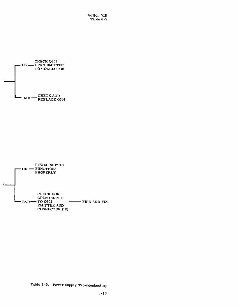
CHECK Q302 OK- OPEN EMITTER
TO COLLECTOR
CHECK AND BAD -REPLACE Q301
POWER SUPPLY OK -FUNCTIONS
PROPERLY
CHECK FOR OPEN CIRCUIT
BAD-TOQ302 EMITTER AND CONNECTOR (12)
Section VITI Table 8-9
---FIND AND FIX
Table 8-9. Power Supply Troubleshooting
8-13

--------- -------" ..... - ........
SEE' INSIDE
•.
Table 8-9
POWER SUPPLY TROUBLESHOOTING
8-13

Section VIII Figure 8-11
8-14
Figure 8-11.
Model 4328A
Model 4328A Ni-Cd Power Supply PC Board

Model 4328A

TABLE 8-10 Ni-Cd POWER SUPPLY TROUBLESHOOTING
MEASURE ±13V , SUPPLY
METER PEGS - MOTHER BOARD
(WHT/ RED, WHT)
POWER SUPPLY CHECK BATTERY --+--OK- FUNCTIONS
PROPERLY
OK·
BAD
METER INDICATES BATTERY _CONNECT 4328A TO_ DISCHARGED AC LINE POWER

D lT)
'4328A TO POWER
CHECK AND OK -REPLACE
A7R 404, R405
CONNECT 4328t' MEASURE VOLTAGE REPLACE BAD- TO AC LINE -ACROSS A6CR405 - FAULTY
- AND A6CR411, AND POWER I CHECK A6R401, A6R402 COMPONENTS
I
I
CHARG~ BATTERY FOR 30IMINUTES
OK- THEN PISCONNECT 4328A Fi'ROM LINE POWER
CHEC~ FUSE, TRAN FORMER
BAD- A6C40 , A6C402 A6CR 01-CR404 A6CR 07-CR410
I
POWER SUPPLY OK - FUNCTlONS
PROPERLY
BATTERY CHECK AND BAD -WON'T -REPLACE
CHARGE BATTERY
FlND BAD-AND
FlX
MEASURE VOLTAGE
OK-ACROSS A6CR405 AND A6CR411
CHECK AND OK-REPLACE
BATTERY
Section VITI Table 8-10
CHECK REPLACE BAD-A6R401 -FAULTY
A6R402 COMPONENTS
Table 8-10. Nt-Cd Power Supply Troubleshooting
8-15

Sf:E INSIDe:
Table 8 -10
NI-Cd POWER SUPPLY TROUBLESHOOTING
8-15
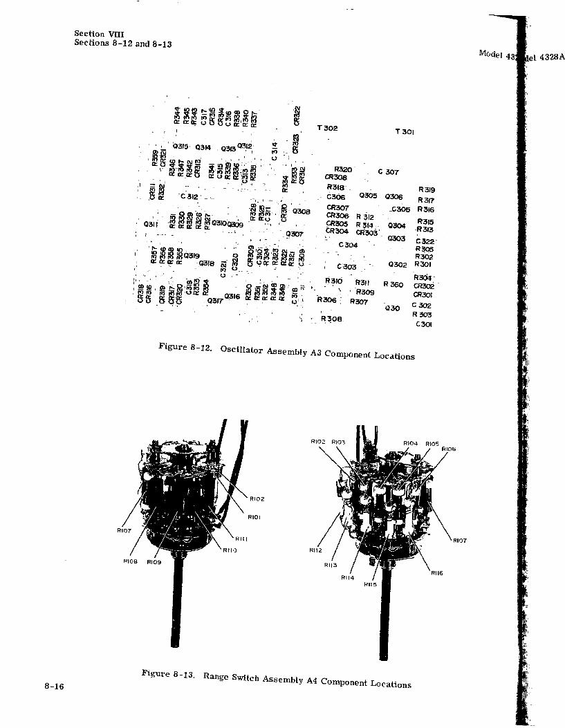
B-16
Section Vlli Sections 8-12 and 8-13
T302
R320 CR308 R318
T301
c 307
R319 C366 Q305 Q306 R 317
CR307 C305 R316 cR306 R 312 CR!505 R 314 , Qao4
~~3p4 CR303, 0303 C304
R315 R313
C322 R305 R302
Q302 R301
Rasa
Q30
R308
R304 CR30.2 CR301
C302 R303 C301
Figure B-12. Oscillator Assembly A3 Component Locations
RI02
RIO I
RIOB RI09
Rll5
Figure 8-13. Range Switch Assembly A4 Component Locations
4328A
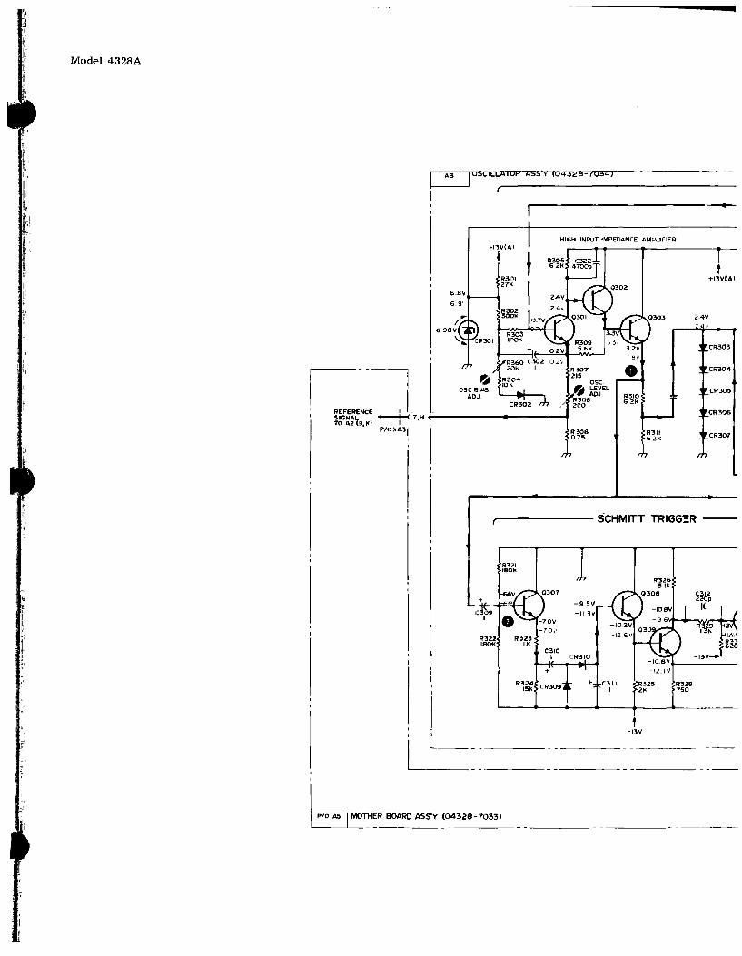
Model 4328A
~DL,A __ •o __ R __ A_s_s_·_v __ to_q __ 3_2_e_-_r __ o_3_4_J ________________________ ___
OSC BIAS AOJ
H3V(A)
• R31ll ~7K
Hl<iH INPUT IMPEDANCE AMPLIFIER
t +13V(A)
2..4V
CR303
CR304
CR:JOS ~~~. I W,G~~~9 !<) ---:-<.7•H +--------.. -----~
' P/OXA31
CR306
CR307
~------SCHMITT TRIGG=:R
L __ _ t ·13V
---------
----------- ------

·----- -------- -
-----------OSCILLATOR----------------------------------------
t +13V(A)
(CR303
(CR304
~CR306
~CR307 7
R312 271<
R327 B2K
._ ___ OIV
5 Ql,,'
CR311
---------
------------
C I I
+
+13(A)--------,
R319 12~
R320 130
POWER AMPLIFIER
,-----CLIPPER--------...
Fl348 681<
R350 ZOK
R351 201<
109V II IV II 7Y
R354 33k
R353 681<
4.ZV
C320 0001~
BLIJ
BRN
1..---..............cBLI<~~~----OETECTOR INP
+13V(B)
'
L ___ . L____-
.----FLIP- FLOP---..
C321 00015
7BV Jlo 7.2v
R357 101<
R358 3901<
'~~-l__jREO BRr
_k II,N
C-.. 41 Eo
R333 911<
CR312
C311 I
1-+
R33"! 1501<
R334 1201<
---------15,5
--~~---------~~--------~~-------r----~~-~--1---------- -LTo A2!Z,BJ}
FLIP- FLOP SIGNAL TO A2 (3,CJ TO PHASE DETECTOR
---- ------------ --------- ------ ------ -------------

DETECTOR INPUT TO T201
- -P/0 XA3
-L5V
R353 911<
CR312
04328
-7033 J5
\ I6143A
L ______ _
R337 C316 47K -~ 5V 0,1
t -13V
R340 101<
------- ------
~AL roR
.-, / I
I I I I
:q-1 I
riP
L~-~L------~~-~ ~ r.,, 1~1 I .. I I --I I ~~--OOL-----+-'"1-"'"T 1, I
-.J
,SAMPLE UNDER TEST
BLU
BRN
BLK
r--A-4---..RANGE SWITCH ASS'Y (04328 -7024)
r--------------------------'
RIO I* 0~ SIOIBR
1121 RIIZ* * (I)
056 RI02 15
* (2) Rl13 039
* (3) Rll4 035
* Rll'5 034
* 15 Rll6 033
50
161
ILl, L_ R122't(B)
--l--l _._:'::R~"-I~0=.9*_1t-'V'~" ~ 151< (10)
----------------~ i L_ L._~ __ .i~1-~-===_~~~=~_~k=-~~=:~=~---_ =_=_ -)_._~_~~~~~
L_ REFERENCE DE
NO PREFIX
C20J,C308 J4 W2
-13V.....,
.I .I i FROM SIA +13V(A)------4. 5 ,E[r' -- +13V
<A3
+13VI8)~12,N;
I I ! r-----4e,~)'l"+l1 ---•• CI,RCUIT COMMON
rfr ·, \rl7)TO A2(6,F,7,HI
I II ~ 6,F )>-~-1!-i --- NO CONTACT
-13V ----71o,L):>---il----- -13V 1 FROM SIB
---------~PfOXA3
CR314
CR315
------------------- __ j COPlRIGHT 1970 Bi" YOtfOGAWA-HEWLETT-PACI't'ARO, LTD
OELETEOrA3C
NOTE
VOLTAGE!
OF SHOR"
RESPECT
AT lmil
BLAC" R
REO REAl
Figure 8-

Section VIII Figure 6-14
'.Y (04 328 -7024)
----------------,--01
IOI* 05 SIOIBR
~I)
~:: 10
~(6) ·- L....-J ~~.~cr. lOb 0 ~0 R121* (7)
90.9~
108 0 SKCJRiz.-(8)
261K
109* ~ < (9)
* ~) k (10)
~ IK (Ill
I
' I
1121
I 5101 I
------------- --------'
N 7,HI
REFERENCE OESIGNA TIONS
NO A3 ASS't PREFI~
C201,C308 qo1-c322 J4 CR301-CR323 W2 0301-0319 lfA3 R301-R360
T30I,T302
DELETED;A3C308
NOTE
A4 Ass·~ AS
RIOI-R122 T303 5101
ASS''t
VOLTAGES OBTAINED UNDER CONDITIONS
OF SHORfED AND OPEN PROBES WITH
RESPECT TO COMMON ( m I RANGE SET
AT lmn
__j ro, LTD
BLACI< READING FOR SHORTED
RED READING FOR OPEN
Figure 8-14_ Oscillator Ass'y A3 Range Switch Ass'y A4
Mother Board Ass'y A5
8-17

SEE INSIOE
Figure 8-14
OSCILLATOR ASS'Y A3 RANGE SWITCH ASS'Y A4
MOTHER BOARD ASS' Y A5
8-17

Section VIll Figure 8-15 & 8-16
,-~ '
r ,, \,.,
~ I I " I I
8-18
·· i'~-1 - ~- tl-1 -I-
Figure 8-15. Phase Sensitive Amplifier Assembly A 2 Component Locations
~A3 XA2
,'',-
I / ' /
",' l C202
T303 ''
. ' j ,-
Figure 8-16. Mother Board Assembly A5 Component Locations
Model 4328A
'~1 ,_'1
~I ,,

I ,, I ,,
Model 4328A
REFERENt-E DESIGNATIONS -NO
A2 A'iS'r A5 ASS't PREFIX
C2,C20J C203 -C217 C202 C308 CR201-CR210 T303 J2,J4 Q20Hl209 <A2 MIOI R20I-R238 T201 T202 wz
DELETED;A2CR205,A2Q20T
NOTE
IIOLTAGES OIITAINED UNDER CONPrTIONS
Of SHORTED AND OPEN PROBES WITH
RESPECT TO COMMONln71 RANGE SET
AT lmll
BLACI< READING FOR SHORTED
RED READING FOR OPEN

PROBE
I I
~SE-- SENSITIVE AMPL-JF_I_E_R_A_S_S_'_y_(0_4_3_2--8--:_~702-2-l ----- --~~~~------------------1 ,. AC AMPLIFIER
I
--~I ~~2.R:
13
I I I I
I le
R205 ZOI<
-2 .. 0V -- C} I
R204 131<
0.204
-f I 5'~-'
R209 471<
-IO .. SV -I [I
C207 R211 561< lOOp
-12 .. 5V -12 5\'
R212 6801<
R210 510
-13V
• C20B 45P,t
+C209 47
R21 751
H214 IBK
t---41---t----~rl;.R R206 0 015
P/OJtA2
R202 1001<
CR201
R208 lOOK
75K
- -13V
~--~--~~~r---·._ ____________ ~
R201 C203
L~"'T., I I
r-----'==o--C-J30~-
L~J OSCILLATOR OUTPUT FROM A3t9,K j
LIMITfER INPUT TO A3(11,M)
C204 0 22
0 14 p 4,0
P/OXAZ-' ~--- --= '?===---+= SCHMirT TRIGG OUTPUf FROM
ORN , lEL A3(13,Pl ,___.,_ --~·----
1 ORN tEL
T202
RED l
------------RED
El MOTHER BOARD AS-=-~43~8-70~~1 _____ _ -------- ------

..----- DC AMPLIFIER a MODULATOR ---__....,. 107V
_14-107"~' 90V 1-6·.,, l
FS .. i 9 .. 0V 0 OADJ R222 6 1-=j\,1
1?213 821< 0208 R2~2 :;.'LIN ~Rzzg 751< 3 . .';v
""I LV Sk-" ADJ.., 201<
G ~2 .. 9V R23o*
* !8 .. 31< R234
-6 ev ti 4 1H 6,811<
Q20(p -6 8'<> Q20g ----- "::t\8 ,~CR20B ...
~ ~-"'" 3 711, \!:- C212 c;~D4 R23B 4 8 \} ----- 3.7V 047 680
-II 4'~ 3..1V 3 8l R227
8 4 ' 20 I ~ I
~1 C210:: RU3 R224 R226 I PHASEAoJ I + lOOK 201< 43 ·,
9,0V I r PHASE DETECTOR , 45V I,
rP MODULATOR I -o.sv Q209 I 209 R214 0 61.'
7 181< i R216 R217
68 II< 6811< II I R22"5* +czl3 ov
201< CR206 53 I
CD I ZERO ADJ 90V-
~
C'!_2,02 c~;;oJ G ..... 6 5~
~llzza ~ ~)09V /' 201< C216
~207 F1215 R219 R218 I 331< IOK 3~1<
Jl R2~1
/ R220 R221 1001< lOOK 4 31< This line Is coMected
to the drcult common
t tmllnA3 C215
I -13V
47 l+cz11 11g~l~ ...
4D 35V • 4 ov 75\.'lorQI,I \ 01-11Df7 5V)
----- , _____ , 11------· ---- - --4,0 2 18 3,C
=-="'=f===-=.2:f=----~ ,.:::==----, SCHMITT TRIGGER FLIP-FLOP SIGNAL FLIP-FLOP SIGNAL
1
OUTPUT FROM FROM A31 15,5 I FROM A3114, R I A3(13,Pl - _j
---------------
C214 I
11235 9091<
R237 2 71<
+
~ ;:\R209
~)09V -~\CR210
~ IIV + -..--'
R236 31(
-
-" /
REC. I OUTPUT
ADJ .. I
0 I
1 L
R2J3 2K
C217 1 I
+ ., I I I
•J r
J /
I I I
J u I I I
I
I
'-------- ----11)-------------~---------------,
a I I I I I
I ! 9,1<>-+--1 i
5,E>-+- .-
I I
I
REFERENCE SIGNAL FROM A3(7,HI
+13V
TO A3(8,J)
-13V -~ I,A>--f---- -13V
I I i I P/0 .:A2
---------------------COPtAIGHf 1970 Bt YO~OiiAWA-HEWLETT-PACICAO, LT[
F1gure 8-17 PhasE
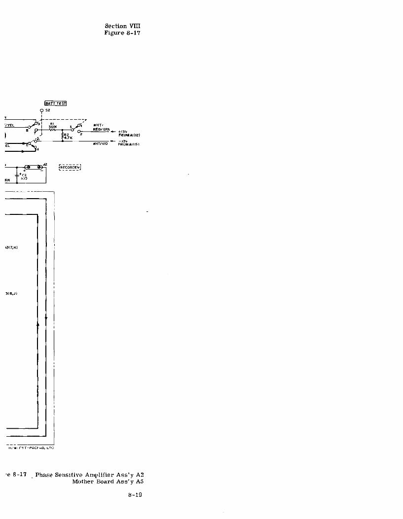
7 )
WHTi
Section VITI Figure 8-17
RED/GRA- +I3 V FROMAI(!l)
:
~·o-';><6-------<~------,w;;;H-;;T;:t;-;;v,:::;-o - F~~~Aifl51 EL~4
RN
13(7,Hl
3IB,Jl
----=;l I
I I
-J -HEWLETf-PACKAO, LTP
·e 8-17 _Phase Sensitive Amplifier Ass'y A2 Mother Board Ass' y A5
8-19

-
SEE INSIDE
·.
Figure 8-17
PHASE SENSITIVE AMPLIFIER ASS'Y A2 MOTHER BOARD ASS'Y A5
8-19

Section VIII Figure 8-18
8-20
i l
'l-
,',!-
t(.l3()2: ~3(), Q303 Q306 Q304 0305 ,, '
-,V
-·~·
-j
-', ,. ,-l
I I ~ I I
Figure 8-18 Power Supply Assembly Al Component Locations
Model 4328A

Model 4328A

REFERENCE DESIGNATIONS
NO PREFilt
Cl 051 Fl Jl MIOI 53 Tl I'll
""' DELETED;
NOTE
AI ASS'r
C301 -C304 CR 301- Cfl310 Q301-Q306 R'301-R309
115 ASS'r
a 50-60Hz LINE INPUT
VOLTAGES SHOWN AFIE REFE"EO TO
COMMONCrhl
PowE:Fi' suPPLY Ass· r (o43o4-7043) 1--A~J ;_W~H~T.:_•':::GR~A:_-... ___ B~L::>:._::R_::E:::_D ______ -0--, T,:, '"'v"'ID,_...,..: 6 .:(-----... 1
115V ........... 230V
GRA
R3 4i"t<
L ___ -: ______ ~p---PIO<AI __ y _________ _J.'
WHr, RED ~'ORN
2
100\,1
4
BLI~ r EL
6
115V
VIO
/ CR304 ...
/
I
J'~ .;,( m3o3 ' / cR302
:7 ( - J
22\1
I
(J301 + 470-25Vl
:8 ~(-----.1 CR309 / ~-CR:l06
"~ A., ----~~g~v-. ______ _
C303 470-25V
+
L---------------------------------------------------------------

~i Co4304-7043)
12
P/0 XAI
::·~~~~------------------ll----------~~1~ j!'JHT RED IJRE
PI'O A5
WHT/RED/ Gr
:o I I I I I I I I I I I I I I I I I I I I I I I
"< ' " i I ! r" :
I I
_j
1 I I I I I I I I I I I I I 1 I 1 I I I
: ! I ), I
L:: __ ~----------------r:~:-ll----------- i~~ ' WHTIVIO o; .,,.. : 0
I I o) I
I i -------r _j
r ____ I
----- l ·C.~---------- u~ 2
1 ,-.__,__ __ -";R~I~-- 7 I cf'l
3 30" I
I I I
I --------~ _L___ 6 I
I 1""1----=Y~E;-L-4
WHTIRED
WHT•'OFIN
Ml
GRN
COP
Figu

+13V
Section Vlll Figure 8-19
~NH~T.,;';.:R.:,:E;.:;D._ ___ -c.:W:.:;H:.:;T.:.,I::,RE~D'-- TO AZ 15, E I 8 11315, E ,12,N)
I -13\1
_;cW.~;~HJ.f-----..(~)-W;;.H"'T"---•TO A2(t,AI6 A3(to,U
I
I
~W~HT~/O~R~N~------~lWHT/ORN I MET+
-METER OUTPUT FROM A21 Jl
' I
---;G:;:R:;-:N:----------1 MET -METER OUTPUT FROM A2 ltO,L) i C___ _ _ ___j
b ' GRN
COPlRIGHT 1970 8 f 'tO~OGAWA-HEWLE rT- PACkARD, LTD
F1gure 8-19 Power Supply Ass 1 y Al Mother Board Ass'y A5
8-21

SEE INSIDE
Figure 8-19
POWER SUPPLY ASS'Y AI MOTHER BOARD ASS'Y A5
8-21

Section VIII Figure 8-20
8-22
,, 11; 1 <t
BT401
~I I
-' - I
BT402 ',
t, : ,''
(i; ,401 "' f 'j' ' "
''
BT404
I~~-
.J' ,_I '· r C 402•r•
.-,
•·BT403
'" " ~'
Figure 8-20 Ni-Cd Power Supply Assembly A6 Component Locations
Model 4328A
•
• I
I'
•

Model 4328A
0
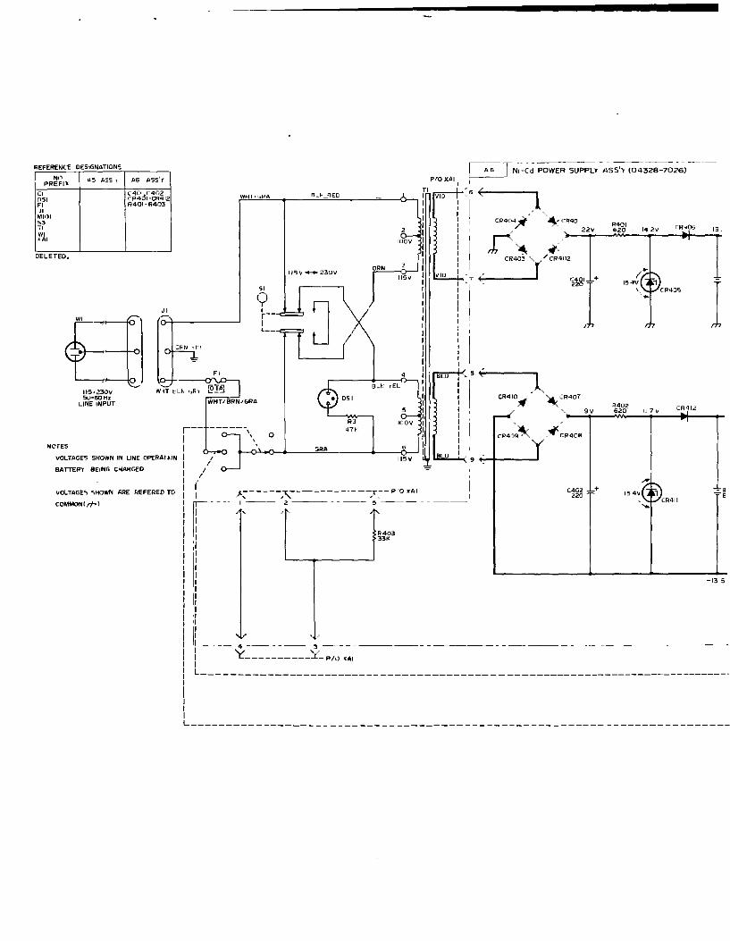
REFERENCE DESIGNATIONS
Nil PREFI1<
A5 ASS' t AG ASS'Y
Cl PSI Fl Jt Mill I 53 Tl WI •AI
DELE rEO,
fl NO rES
115t230V 50-60Hz
LINE INPUT
J I
VOLTAGES SHOWN IN UNE OPERAHJN
BA TTERt BEING CHARGED
,--1 I I I I
WHT• GRA
5I
q I r--1 L--
WH rt BRN IGRA
0
PlO )(AI I
BU·__£JED
11'5V....,..23DV
47~
GRA
I " VOLTAGES SHOWN ARE REFEREO TO I j COMMON(f'hl I I A----- ---------1 r---- I- - ,"'\; ---r--P'OXAI J I I ' 2 --- -- --- ··~' -----
I I ' --
1 I I I R403
33K I 'I I 'I I I I I I J I I I I I I I I I I I 'I I 'I
IL I I I I I I I L_ I
I I I I L----
4 -------Y' ---,_-3 ----__________ y_P/0 <AI
POWER SUPPLl' A ' - -55 y (04328-7026) --
l 8 (
~ CR410 * ~ CR407
~----~9rV----11
~64
N2~~2
--~Il~7~V~--~C·R4!1~2~----)i(' CR408
C402 + 220 15 4V
'"-., CR411
-13,5

-----B28-7026)
14"2V CR406
07V CR412
... CR411
r35V
- BT401
r~
OV
- BT403 -BT404
-13 sv
PtO_.AI I I +13V
12) 1, WHT/REO ORE
I
WHT,'REO WHTIREO o--------------~~~----~~~
I
I ~13
I 14
'
I I I I I I I I I I I I I I
I I P,'O A5 I I
I I I
LHU BL~ l WHTIBLI<
I MoniER BOARD "ASS't (04328 -7033)
~ -~
r l I I ' :~ I .____ __ _j
C I
1001
WHT •' REO ,•' GT
""-o
I I I I I I I
0
15~/----------------------~------,_------------a~~~ o I I WHT'VIO I i"' 10 >l r :
I I I 0
wr
,)-1 I ________ j ! !
WHTlORN WHT/ORN MET+ r------1-- ----I ------- ____ j
---------------------------------------- _61 52
91 9~~~----~W~HTllLJ~fE8L~I 2 ~ I"
D---.------~~--------o~ I e
I LINE FASTl ON- OFF- CHARG~
o1"' 3 3'&1. 7 \ 1
' I i R2 I I 471< 1
--------------~------1------TL---r-------------l ----------------------- I 6 :
I :1, ~----=:"---" I 4 5 TEL I
Qs3 1 BATT TEST I
GF!N GRN MET-
COP'YRIGHT 1970 E
Figure 8-21 Ni-C
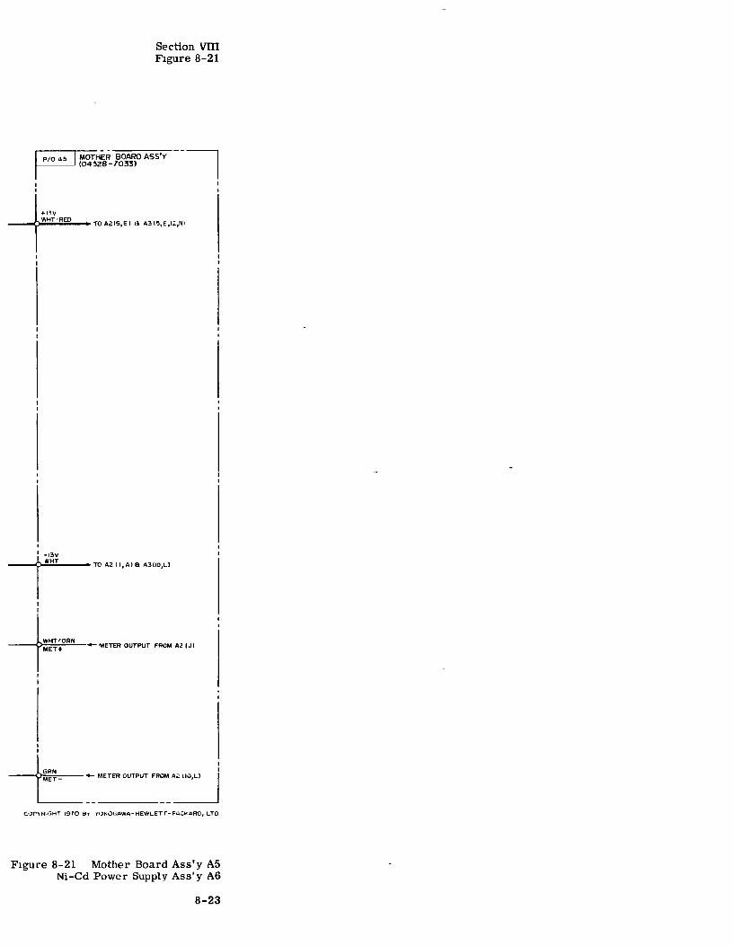
+13V
Section Vlll F1gure 8-21
--.-..<~W:;_:H~T~'R:;:E;:;D;__ TOA2(5,El 8 A3t'5,E.121N)
I
I -13V
lm"''·""•""·" I I
---07=':::~'::~:'::.:;D;..:R:_:N __ METER OUTPUT FROM A21JI
I I
t I I
~METER OUTPUT FR:~ ::J COPYRIGHr 1970 BY Yl)kOGAWA-HEWLETr-PACKARD, LTD
Figure 8-21 Mother Board Ass'y A5 Ni-Cd Power Supply Ass 1 y A6
8-23