MILAD MOSALLAEI Improving the Electrical Performance of ...
101
Tampere University Dissertations 341 Improving the Electrical Performance of Printed Stretchable Interconnects by Local 0RGL¿FDWLRQ RI 6WLႇQHVV MILAD MOSALLAEI
Transcript of MILAD MOSALLAEI Improving the Electrical Performance of ...

Tampere University Dissertations 341
Improving the Electrical Performance of
Printed Stretchable Interconnects by Local
MILAD MOSALLAEI


Tampere University Dissertations 341
MILAD MOSALLAEI
Improving the Electrical Performance of Printed Stretchable Interconnects
by Local Modification of Stiffness
ACADEMIC DISSERTATION To be presented, with the permission of
the Faculty of Information Technology and Communication Sciences of Tampere University,
for public discussion in the Auditorium S2 of the Sähkötalo, Korkeakoulunkatu 3, Tampere,
on 27.11.2020, at 12 o’clock.

ACADEMIC DISSERTATION Tampere University, Faculty of Information Technology and Communication Sciences Finland Responsible supervisor and Custos
Professor Matti Mäntysalo Tampere University Finland
Pre-examiners Professor Stephen Beeby University of Southampton United Kingdom
Assoc. Professor Woo Soo Kim Simon Fraser University Canada
Opponent Professor Jan Vanfleteren Ghent University Belgium
The originality of this thesis has been checked using the Turnitin OriginalityCheck service. Copyright ©2020 author Cover design: Roihu Inc. ISBN 978-952-03-1765-2 (print) ISBN 978-952-03-1766-9 (pdf) ISSN 2489-9860 (print) ISSN 2490-0028 (pdf) http://urn.fi/URN:ISBN:978-952-03-1766-9 PunaMusta Oy – Yliopistopaino Vantaa 2020

iii
ACKNOWLEDGEMENTS
This research work was carried out at the Laboratory for Future Electronics at Tampere University, Finland, from 2016 to 2020. The research was funded by Disappearing Sensors (Tekes), Elastronics (Business Finland), and EpiPrint (Academy of Finland). This research utilized the research infrastructure PII supported by Academy of Finland (AoF FIRI: PII, 320019). The financial support is greatly acknowledged.
First of all, I would like to say a very big thank you to my supervisor Prof. Matti Mäntysalo for his trust, support and guidance throughout my work. I am extremely grateful to all my co-authors Prof. Jukka Vanhala, Prof. Minnamari Vippola, Assoc. Prof. Mikko Kanerva, Dr. Mari Honkanen, Dr. Behnam Khorramdel, M.Sc. Pekka Iso-Ketla and especially Dr. Jarno Jokinen and Dr. Donato Di Vito. I express my warmest gratitude to Prof. Donald Lupo and Prof. Paul Berger for their knowledge. It was a great experience working with them during my master studies. I would like to extend my sincere thanks to Dr. Jari Keskinen for his knowledge and his amazing character. I am forever thankful to my colleagues at the Laboratory for Future Electronics. All of them are very friendly and great people and I was so lucky to work with them.
It is a pleasure to thank and appreciate my beloved friends especially Hossein, Farid, Vafa, Behnam, Maedeh, Patryk, Ewa, Kiarash, Zahra and Afshin. I would like to express my gratitude for Prof. G. Steven Bova and his lovely wife, Eunchung. Steve! You are one of those people who make my life better by just being in it.
At the end, my deep and sincere gratitude to my family for their continuous and unique love, help and support. I especially would like to express my deepest appreciation to my amazing fiancée, Paula as without her support I may never have completed this thesis. Tampere, October 2020.
Milad Mosallaei

iv

v
ABSTRACT
For the production of stretchable electronics, the development of advanced materials which can be adaptable to deformation, as well as tailoring of the structural designs, fabrication and characterization strategies for soft materials are all needed. The major challenge is the ability of the device to maintain both the mechanical and electrical performance during the deformation for a desired number of cycles, and each of the aforementioned requirements are essential to respond to this challenge. From the fabrication point of view, although printing is heavily employed for stretchable electronics, fully printed circuit devices still need further improvements due to their response time, low integration density, etc. To overcome these limitations, heterogonous integration is a potential solution combining the advantages of printing techniques found in the production of large area electronics with the high performance of conventional inorganic electronic devices. In this regard, the island-bridge concept provides links between miniaturized functional units using stretchable interconnects on compliant substrates. Therefore, the development of reliable, stretchable interconnections is highly sought after.
This thesis focuses on an investigation of the practical approaches to improving the electromechanical performance of screen-printed, stretchable interconnects based on carbon and silver inks. Initially, stretchable carbon interconnects were screen-printed, and then methods and tools for the electromechanical characterization of the samples were tested and verified. After this stage, the concept of a “sacrificial zone” was introduced in this thesis where it was shown to improve the stretching performance of interconnections from 44% to 54%.
In the following studies, the “local tuning of the stiffness” by adding and removing material was investigated. This approach had positive effects on the rigid-soft interface by mitigating the strain in this location and improving the homogenous distribution of the stress in the system. The approach can be used in heterogenous integrations, where it was demonstrated to improve the stretching performance from 22% to 43% in the case of passive component attachments.

vi

vii
CONTENTS
Acknowledgements Abstract List of figures List of tables Abbreviations List of publications
1 Introduction ............................................................................................................................ 1 1.1 Aim and scope of the thesis ..................................................................................... 2 1.2 Structure of the thesis ............................................................................................... 2 1.3 The author’s contribution......................................................................................... 3
2 Background ............................................................................................................................. 5 2.1 Stretchable electronics and stretchable interconnects ......................................... 5 2.2 Materials for fabrication of printed stretchable interconnects ........................... 8 2.3 Fabrication techniques ............................................................................................ 15 2.4 Mechanical design .................................................................................................... 21 2.5 Reliability and failure analyses................................................................................ 25 2.6 FE analyses ............................................................................................................... 30
3 Results and discussion ......................................................................................................... 37 3.1 Fabrication and characterization of stretchable interconnects ......................... 38 3.2 Modification of conductive line ............................................................................ 39 3.3 Modification of local stiffness by adding encapsulation ................................... 43 3.4 Modification of local stiffness by removing material ........................................ 51
4 Conclusion ............................................................................................................................. 55

viii
List of Figures Figure 1 Examples of stretchable applications requiring stretchable
interconnects (a) Stretchable interconnects based on a MWCNT-PDMS nanocomposite [27], © IOP Publishing. Reproduced with permission. All rights reserved. (b) Artificial skin for a prosthetic hand [32]. (c)Balloon catheter integrated with electrodes and temperature sensors [39]. (d)Thermal monitoring sensor system for human skin [33].(e) Strain sensor integrated with a bandage and glove [34]. (f) Stretchable chemical sensor for sweat detection [35]. (g)Stretchable display based on an inorganic LED. From [36]. Reprinted with permission from AAAS. (h) Stretchable circuits for EEG signal detection and transmission. From [37]. Reprinted with permission from AAAS; and(i)a stretchable transistor matrix. From [38]. Reprinted with permission from AAAS. .................................................................................................. 7
Figure 2 Comparison of the elastic modulus and electrical conductivity of some common materials used for the fabrication of stretchable interconnects (PET: Polyethylene terephthalate, PMMA: Poly(methyl methacrylate), PP: Polypropylene, PS: Polystyrene, PC: Polycarbonate, PDMS: Polydimethylsiloxane, PU: Polyurethane, PEDOT:PSS Poly(3,4-ethylenedioxythiophene): polystyrene sulfonate, Cu: copper, AU: gold , Ag: silver, CNT: carbon nanotube). [27] © IOP Publishing. Reproduced with permission. All rights reserved .............................................................................. 9
Figure 3 Schematic representation of A: ACA, B: ICA and C: NCA in flip-chip assembly [73], D: Conductivity of different adhesive versus filler concentration based on percolation theory. .............................................................. 14
Figure 4 Schematic illustration of A: parameters in the screen printing process, B: rotary screen printing [43]. ............................................................................................ 17
Figure 5 Screen printers used for printing of the devices for the publications of this thesis A: semi-automatic TIC SCF 300, B: fully automatic Ekra X5 Professional. .................................................................................................................... 18
Figure 6 A summary of structural designs that accommodate stretchability, a: wavy and wrinkled design [104], b: network design [104], c: fractal-inspired design. Adopted from [107], d: island-bridge design, Takao Someya: Stretchable Electronics. Page: 145. 2012. Copyright Wiley-VCH GmbH. Reproduced with permission [30], e: kirigami and origami designs [104], [108]. ........................................................................................................ 22
Figure 7 Set-up for electromechanical assessment used in this thesis. A: an Instron 4411 Universal Testing Machine, B: a static clamp, C: a moving
ix
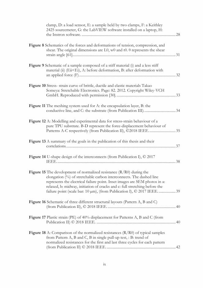
clamp, D: a load sensor, E: a sample held by two clamps, F: a Keithley 2425 sourcemeter, G: the LabVIEW software installed on a laptop, H: the Instron software. ..................................................................................................... 28
Figure 8 Schematics of the forces and deformations of tension, compression, and shear. The original dimensions are L0, w0 and t0. θ represents the shear strain angle [61]............................................................................................................... 31
Figure 9 Schematic of a sample composed of a stiff material (i) and a less stiff material (ii) (Eii<Ei), A: before deformation, B: after deformation with an applied force (F). ....................................................................................................... 32
Figure 10 Stress- strain curve of brittle, ductile and elastic materials Takao Someya: Stretchable Electronics. Page: 82. 2012. Copyright Wiley-VCH GmbH. Reproduced with permission [30]. ............................................................... 33
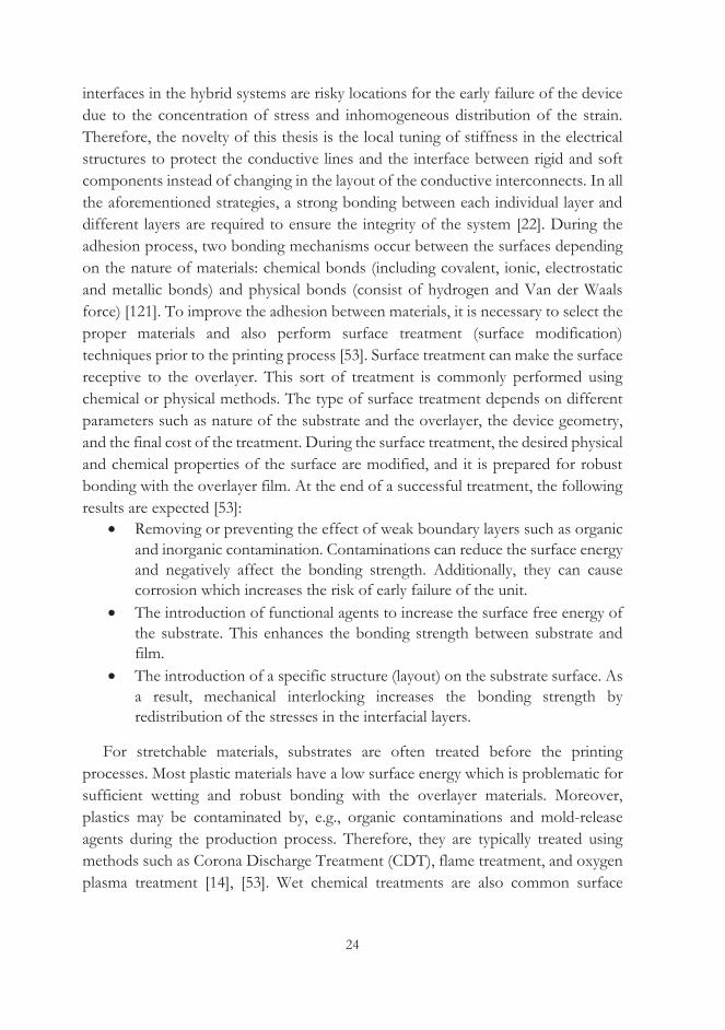
Figure 11 The meshing system used for A: the encapsulation layer, B: the conductive line, and C: the substrate (from Publication III). ................................. 34
Figure 12 A: Modelling and experimental data for stress-strain behaviour of a pure TPU substrate. B-D represent the force-displacement behaviour of Patterns A-C respectively (from Publication II), ©2018 IEEE. ............................ 35
Figure 13 A summary of the goals in the publication of this thesis and their correlations. ..................................................................................................................... 37
Figure 14 U-shape design of the interconnects (from Publication I), © 2017 IEEE. ............................................................................................................................... 38
Figure 15 The development of normalized resistance (R/R0) during the elongation (%) of stretchable carbon interconnects. The dashed line represents the electrical failure point. Inset images are SEM photos in a: relaxed, b: midway, initiation of cracks and c: full stretching before the failure point (scale bar: 10 μm), (from Publication I), © 2017 IEEE. .................. 39
Figure 16 Schematic of three different structural layouts (Pattern A, B and C) (from Publication II), © 2018 IEEE. ......................................................................... 40
Figure 17 Plastic strain (PE) of 40% displacement for Patterns A, B and C (from Publication II) © 2018 IEEE. ..................................................................................... 40
Figure 18 A: Comparison of the normalized resistances (R/R0) of typical samples from Pattern A, B and C, B in single pull-up test, : B: trend of normalized resistances for the first and last three cycles for each pattern (from Publication II) © 2018 IEEE. .......................................................................... 42

x
Figure 19 An FESEM image of the surface of the conductive track on the TPU substrate in its un-stretched form for A: a fresh sample, B: a sample after 1000 cycles and C: an FIBSEM image of the cross section of the conductive track on the TPU substrate (from Publication II), © 2018 IEEE. ............................................................................................................................... 43
Figure 20 Schematic illustration of stretchable interconnects. A: a non-encapsulated sample, B: an entirely encapsulated sample, C: a partially encapsulated sample (from Publication III). ............................................................. 44
Figure 21 The failure location on the printed conductive track after the critical plastic strain (PE) limit (from Publication III). ......................................................... 45
Figure 22 A summary of the stretchability preference of interconnects. A: an interval plot of the stretchability of different sets of samples, 1: non-encapsulated, 2: partially ink-encapsulated, 3: entirely ink-encapsulated, 4: partially TPU-encapsulated and 5: entirely TPU-encapsulated, B: typical performance for normalized resistance of each sample set (from Publication III). .............................................................................................................. 46
Figure 23 The normalized/absolute resistance of the partially TPU-encapsulated samples for 20% stretching cycles (from Publication III). ...................................... 47
Figure 24 The schematic of layouts for stretchable interconnects used in this thesis (from Publication IV and Publication V, right part: © IOP Publishing. Reproduced with permission. All rights reserved). .............................. 48
Figure 25 A: Details of the deformed shapes for the different designs next to the SMD components; the entity plotted is the true strain in the X-direction, which is coaxial with the loading direction, B: Plot of the true strain along the X-direction via the conductive wire, starting from conductive track next to the SMD (from Publication IV). ..................................... 49
Figure 26 A: Normalized resistance (R/R0) of typical samples from different designs in a single pull-up test, B: box and whiskers plot for the stretchability of different samples (from Publication IV). ...................................... 50
Figure 27 A: The FE analyses for the true strain at the maximum location of deformation for different samples (at a strain of 0.4). B and C: progress of the true strain on the conductive track from near the SMD (highlighted by yellow lines) for Set A and Set B respectively (at a strain of 0.4), D: DIC analyses of the strain field for different samples sets. E: development of the stain on the silver tracks in different sample sets (from Publication V, © IOP Publishing. Reproduced with permission. All rights reserved). ........................................................................................................ 52

xi
Figure 28 A: A summary of stretchability plotted for 10 samples for different samples sets, B: Schematic illustration of cross section of a sample in the SMD area, C and D: an SEM image of a fresh sample and one with 1000 cycles at 20% (debonding of ICA from the conductive track is highlighted) (from Publication V, © IOP Publishing. Reproduced with permission. All rights reserved). .................................................................................. 53
List of Tables
Table 1 Conductive and dielectric inks used in the publications of this thesis. .................... 10
Table 2 Properties of the TPU (U4201) used in the publications of this thesis. .................. 12
Table 3 Comparison of common printing methods, adopted from [5], [43], [85]. .............. 15
Table 4 Properties of screen used in this thesis. ........................................................................ 19
Table 5 Parameters used in Ekra screen printer. ........................................................................ 20
Table 6 Standard tests for flexible and stretchable electronics. Adopted from [127]. ................................................................................................................................. 25
Table 7 Properties of the substrate and conductive material used in the FE analysis (from Publication V, © IOP Publishing. Reproduced with permission. All rights reserved). .................................................................................. 36
Table 8 Number of cycles before failure (sets 1–5) (from Publication III). .......................... 47

xii
ABBREVIATIONS
ACA Anisotropic Conductive Adhesive ACF Anisotropic Conductive Film Ag Silver AgNWs Silver Nanowires ASTM American Society for Testing and Materials Au Gold CDT Corona Discharge Treatment CNTs Carbon Nanotubes CTE Coefficient of Thermal Expansion Cu Copper DIC Digital Image Correlation DMA Dynamic Mechanical Analysis E Young’s Modulus (Modulus of Elasticity) ECA Electrically Conductive Adhesive ECG Electrocardiogram EEG Electroencephalogram EGaIn Eutectic Gallium-Indium EPDM Ethylene Propylene Diene Monomer FE Finite Element ICA Isotropic Conductive Adhesive IEEE Institute of Electrical and Electronics Engineers ISO International Organization for Standardization OLED Organic Light-Emitting Diode OPV Organic Photovoltaic LiCl-PAM Lithium chloride-polyacrylamide NCA Non-Conductive Adhesive PANi Polyaniline PC Polycarbonate PDMS Polydimethylsiloxane PE Plastic Strain

xiii
PEDOT: PSS Poly(3,4-ethylenedioxythiophene): polystyrene sulfonate PEN Polyethylene naphthalate PET Polyethylene terephthalate PI Polyimide PMMA Poly(methyl methacrylate) PP Polypropylene PS Polystyrene Pt Platinum PT Polythiophene PU Polyurethane R2R Roll-to-roll SAC Sn-Ag-Cu SEM Scanning Electron Microscope SMD Surface Mount Device Sn Tin Tg Glass Transition Temperature TPU Thermoplastic polyurethane UV Ultraviolet ε Strain σ Stress ν Poisson’s ratio

xiv

xv
LIST OF PUBLICATIONS
Publication I. M. Mosallaei, B. Khorramdel, M. Honkanen, P. Iso-Ketola, J. Vanhala, and M. Mäntysalo, “Fabrication and characterization of screen printed stretchable carbon interconnects,” in 2017 IMAPS Nordic Conference on Microelectronics Packaging (NordPac), 2017, pp. 78–83
Publication II. M. Mosallaei et al., “Geometry Analysis in Screen-Printed Stretchable Interconnects,” IEEE Trans. Components, Packag. Manuf. Technol., pp. 1344 - 1352, 2018
Publication III. M. Mosallaei, J. Jokinen, M. Kanerva, and M. Mäntysalo, “The Effect of Encapsulation Geometry on the Performance of Stretchable Interconnects,” Micromachines, vol. 9, no. 12, p. 645, Dec. 2018
Publication IV. 4 D. Di Vito, M. Mosallaei, B. Khorramdel, M. Kanerva and M. Mäntysalo, “Mechanically driven strategies to improve electromechanical behaviour”, Sci. Rep., vol 10, no. 1, p.12037, Dec. 2020
Publication V. M. Mosallaei, D. Di Vito, B. Khorramdel, and M. Mäntysalo, “Improvements in the electromechanical properties of stretchable interconnects by locally tuning the stiffness,” Flex. Print. Electron., Jan. 2020

xvi

1
1 INTRODUCTION
Common electronic devices are mostly bulky and non-deformable as they are often fabricated on rigid substrates such as glass or silicon [1]. The main reasons for the physical state of these applications are the rigidity of the constituent materials and the manufacturing methods that are employed to fabricate them. The rigidity of conventional electronics limits their use in applications where mechanical deformability is required [2]. For example, devices attached to human skin need to be highly adaptable to the uneven and stretchable nature of the skin [3]. Similarly, sensors in the joint parts of robotics should be highly stretchable to accommodate the folding and twisting motions of the joints [4]. There is significant demand for the development of such applications using low cost fabrication techniques common to the production of large area electronics. Printed electronics are commonly used to fabricate electronic circuits on stretchable, conformable, and flexible substrates such as plastics, textiles, and papers. These methods bring advantages including cost-effectiveness, high throughput, light weight, and disposability of the devices [5], [6]. However, fully printed devices suffer from a lower electrical performance (e.g., slower response time), and a lower integration density in comparison to silicon-based counterparts [7]. Heterogeneous integration is a convenient way to merge the high-performance of conventional silicon-based electronics with the cost effectiveness and conformability of printed electronics [8], [9]. The Institute of Electrical and Electronics Engineers (IEEE) has defined heterogenous integrations as the “integration of separately manufactured components into a higher-level assembly that, in the aggregate, provides enhanced functionality and improved operating characteristics” [10].
A common way to make stretchable electronics is through the miniaturization of functional units while they are still rigid and then to link them together using stretchable interconnects. Establishing a reliable interconnection between components to maintain either the mechanical integrity or electrical conductivity during the stretching is therefore crucial. Employing deformable materials and engineering the design are primary requirements for the fabrication of such stretchable interconnects.
2
1.1 Aim and scope of the thesis
This thesis investigates the effect of the structural design of interconnections on the heterogeneous integration of rigid and deformable materials. The aim is to fabricate stretchable interconnects for wearable structures for items such as health patches or textiles, for example. In such applications, the strain level is limited to approximately 15%–20% which is typical for normal movement on human skin. Thus, the aim was to fabricate devices to approach this deformability level as the minimum requirement and to be compatible with production techniques for large area electronics such as printing production. The novelty of this study is the easily adaptable local tuning of the stiffness in electrical structures to protect the conductive lines and interface between rigid and soft components, and hence improving the reliability of the devices. Initially, the electromechanical testing methods were improved and verified by the characterization of stretchable interconnects. Then three scenarios to accommodate a narrow-to-wide transition along the interconnects were investigated by means of changes in the geometry of the conductive and encapsulation materials where a new design concept involving areas called “sacrificial zones” was developed. Then rigid surface mount components were added to the stretchable interconnects to study the influence of the rigid-soft interface. Such devices are highly prone to early failure in this interface because of the accumulation of stress. Therefore, two approaches were investigated to reduce the stress and strain concentration in close proximity of the rigid-soft interface by locally tuning the substrate stiffness so that both approaches could successfully improve the electromechanical performances of the stretchable interconnects. The modified stretchable interconnects with/without rigid components could achieve an average single pull-up value of 59.8% and 44% respectively.
1.2 Structure of the thesis
This thesis is divided into three chapters followed by a conclusion. The publications included in this thesis are also added. The first chapter introduces the agenda of the thesis and a brief discussion on its aim and scope, followed by the author’s

3
contribution to the publications used to prepare this thesis. The second chapter presents the background regarding stretchable electronic materials and fabrication techniques. The mechanical design, reliability, failure analyses, and finite element analyses are also discussed in this chapter. Chapter three explains the results that were investigated in this thesis. The last chapter summarizes all of the studies done in this thesis and the developments that are required to continue the work in the future.
1.3 The author’s contribution
Publication I. The author was the main contributor, fabricated and characterized the interconnects, and optimized the fabrication and characterization methods. B. Khorramdel and M. Honkanen helped for the SEM sample preparation and image acquisition. The manuscript was written by the main author and revised and improved by M. Mäntysalo. Publication II. The author was the main contributor and designed, fabricated, and measured the test structures, analyzed the data, and wrote the manuscript. He performed the mechanical tests and provided the parameters for the modelling, as well as comparison of the data between the modelling and experimental part. J. Jokinen performed the FE analyses and wrote the relevant section. M. Honkanen took SEM images. Other authors revised and improved the manuscript. Publication III. This paper continues the work in Publication II. The author was the main contributor of the work and designed, fabricated, and analyzed the data acquired from the characterization tests. J. Jokinen performed the FE analyses and wrote a section of the paper. M. Kanerva and M. Mäntysalo revised and improved the manuscript. Publication IV. The author was a co-contributor, and fabricated and characterized
the samples. He wrote the relevant chapter in the manuscript regarding the
preparation and characterization of the samples. The chapter was then revised and
improved by other co-authors.

4
Publication V. The paper continued the work in Publication IV. The author was the main contributor of the work and wrote the manuscript. He prepared and designed the layout of samples, took the SEM images, designed the characterization methods, and analyzed the data and verified the accordance of the modeling results with the experimental data. D. Di Vito performed the FE analyses, took the DIC images, and wrote a section of the paper. B. Khorramdel reviewed the manuscript and M. Mäntysalo revised and improved the manuscript.

5
2 BACKGROUND
The growing interest in the development of stretchable electronics has motivated researchers to innovate new materials, mechanical designs, and fabrication methods compatible with soft electronics. A truly stretchable application should be able to undergo different kinds of deformation (e.g., stretching, compression, twisting, etc.,) during their lifecycles and still maintain their functionalities. Linking the functional circuits by stretchable interconnects on compliant substrates is a common approach to the fabrication of stretchable electronics. Therefore, stretchable interconnections have become an essential component in the development of stretchable devices such as epidermal electronics.
2.1 Stretchable electronics and stretchable interconnects
Conventional electronics are rigid and non-deformable, although they have high levels of reliability during their service life [11]. The materials, layouts, and their reliability are well-studied and they serve extensively in a variety of applications such as household appliances, the automotive industry, etc. [12]. However, with the advancement of technology, there is a big need to develop potential applications that facilitate some degree of mechanical deformation unlike traditional silicon-based structures [11], [13]. Therefore, in the last few years research, industry, and the market have been paid a lot of attention to the development of stretchable electronic devices [14], [15]. In principle, stretchable electronics are soft devices that are able to undergo different types of deformation such as bending, stretching, twisting, compressing, and conforming to non-planer surfaces while they still maintain their mechanical integrity and electrical functionalities [16]. Stretchable electronics provide more freedom than flexible electronics which can only withstand bending [17], [18]. Wearable electronics are potential candidates to take advantages of stretchable electronics. Wearable electronics are actually defined as electronic devices that can be either integrated into a textile or directly attach to the human skin, so they are designed to be in contact with the human body [19], [20] Stretchability is therefore required in these novel wearable applications including body worn

6
applications (skin patches or devices) and smart textile (integration of various sensors and electronics on textiles) devices [21], [22]. These applications are especially important in the healthcare industry where devices can measure and record the vital signs of a patient such as ECG/EEG monitoring [23], human body temperature measurement [24], and sweat analyses [25] and wirelessly transfer the readings to the health monitoring centers [12], [26]. Employing rigid materials for these applications not only brings discomfort to the users but it is also not feasible to use them on some highly-deformable and uneven parts of the body such as on the elbows or knees where device must undergo a large amount of deformation during its lifetime [27], [28].
Individual devices (functional units) can be integrated by using stretchable interconnects [29]. Therefore, deformability of the interconnects to maintain the electrical conductivity between the functional units plays a key role in facilitating the stretchability of the whole system [27]. Ideally, interconnections should adopt the strain of the substrate and maintain mechanical integrity during the stretching and relaxing with minimum change in the electrical resistance for a large number of loading/unloading cycles [22], [30]. The deformation needs to occur along stretchable interconnects between all rigid components [31]. The level of the required stretchability for applications is different based on their functionalities. For instance, a device attached to the knee requires a larger magnitude of stretchability compared to one attached to the chest. Figure 1 summarizes common applications where stretchable interconnects are used [27], [32]–[39]. According to the literature, there are three main wearable technology categories including wearable consumer electronics, health related wearable applications and textile based wearables [40]. The aim of this thesis is to develop the stretchable systems needed in wearable health applications (e.g., skin mounted ECG patch [41]) and textile based applications (e.g., shirts with integrated sensors). In these two categories of wearable electronics, a strain level between 15% and 20% is expected due to the normal movement of the human skin which depends on its location on the human body [42].

7
Figure 1 Examples of stretchable applications requiring stretchable interconnects (a) Stretchable interconnects based on a MWCNT-PDMS nanocomposite [27], © IOP Publishing. Reproduced with permission. All rights reserved. (b) Artificial skin for a prosthetic hand [32]. (c)Balloon catheter integrated with electrodes and temperature sensors [39]. (d)Thermal monitoring sensor system for human skin [33].(e) Strain sensor integrated with a bandage and glove [34]. (f) Stretchable chemical sensor for sweat detection [35]. (g)Stretchable display based on an inorganic LED. From [36]. Reprinted with permission from AAAS. (h) Stretchable circuits for EEG signal detection and transmission. From [37]. Reprinted with permission from AAAS; and(i)a stretchable transistor matrix. From [38]. Reprinted with permission from AAAS.
There are various requirements to fabricate stretchable applications such as the need for deformable materials, engineered structures and characterization methods [11]. The proper selection of materials to facilitate deformation is crucial for all constituents of stretchable applications such as the substrate and conductive materials [27]. Since stretchable electronics are fabricated using different materials with different physical and mechanical properties, precise structural designs are required to facilitate the integration of functional components on compliant substrates [14]. In addition, as most of the available fabrication equipment and characterization tools have been designed for conventional electronics, the development and customization of compatible fabrication and characterization tools

8
are also required [14], [43]. Each of these requirements have their own challenges since if stretchable devices are fabricated using novel materials, engineered designs, and fabrication methods, the manufacturing complexity, overall cost and scalability can limit their usage in mass production [31].
2.2 Materials for fabrication of printed stretchable interconnects
Stretchable electronics have the unique ability to undergo a desired number of loading/unloading conditions during their service life. The soft nature of these devices allows them to adapt and conform to uneven surfaces such as human skin. The materials employed in conventional electronics are inheritably rigid, which limits their use in the fabrication of stretchable electronics. Therefore, the development of new materials with mechanical deformability is highly desired.
In conventional rigid-based electronic applications, metals (e.g., gold and copper) are widely used for their excellent electrical conductivity and thermal stability [44]. Although these materials are highly reliable, it is not feasible to use them in stretchable electronics due to their high Young’s modulus (~ 100 GPa) in bulk form [45], [46]. The hard nature of these materials prevents them from stretching elastically more than a tensile strain of 1% maximum [11]. In fact, metals are normally ductile, and they can undergo plastic deformation up to considerable values of 30% in cases such as copper, gold and silver as discussed in the FE analyses in section 2.6 (Figure 10) [47]. However, when the plastic deformation happens, the material is deformed permanently, and this is not desirable in stretchable electronics as the device should undergo a great deal of loading and unloading during their service life. To increase the mechanical flexibility of these materials, one common means is to prepare a composite ink of conductive particles. In such a system, conductive fillers are distributed into a matrix of rubbery materials (e.g., a polymer) and solvent. Silver nanowires (AgNWs), silver (Ag) flakes, and carbon nanotubes (CNTs) are common conductive fillers [5], [48]. Conductive polymers such as Polyaniline (PANi) Polythiophenes (PTs) and Poly(3,4-ethylenedioxythiophene): poly(4-styrenesulfonate) (PEDOT: PSS) are other options due to their intrinsic mechanical flexibility and transparency. The conductivity level of these organic materials is not high though (~100 S/cm) [20], [49], [50]. Other options as conductive materials include liquid metals (e.g., EGaIn) and ionic hydrogels (e.g., LiCl-PAM) [51], [52]. Figure 2 shows a comparison of the elastic properties and electrical conductivity of common materials used in the fabrication of stretchable electronics [27].

9
Figure 2 Comparison of the elastic modulus and electrical conductivity of some common materials used for the fabrication of stretchable interconnects (PET: Polyethylene terephthalate, PMMA: Poly(methyl methacrylate), PP: Polypropylene, PS: Polystyrene, PC: Polycarbonate, PDMS: Polydimethylsiloxane, PU: Polyurethane, PEDOT:PSS Poly(3,4-ethylenedioxythiophene): polystyrene sulfonate, Cu: copper, AU: gold , Ag: silver, CNT: carbon nanotube). [27] © IOP Publishing. Reproduced with permission. All rights reserved
In a typical printable ink, functional materials (e.g., conductive flakes) are dissolved in solutions together with other additives such as surfactants, curing initiators, etc. [5], [53]. Organic binders are also added to improve the printability of the ink and ensure mechanical integrity and robust adhesion to the substrate [54]. Different properties such as the viscosity of the ink, the type and ratio of binder (and solvent), as well as the type, size, and density of functional fillers all directly affect the conductivity and stretchability of the conductive ink once it is deposited on a flexible substrate [55]. Among the conductive inks, silver (Ag)-based inks are the most common in printed electronics since they demonstrate good physical and electrical performance on plastic substrates [54], [56]. After printing the ink, post-treatment (curing) is required to remove solvents and other unwanted components to achieve the desired functionalities [5], [54]. The materials of the ink and substrate determine the appropriate curing method. The curing process can be performed in an oven if the required temperature and time for the curing are compatible with the constituent components [54]. High curing temperatures damage plastic foils (e.g., TPU, PET, etc.) since they have relatively low glass transition temperatures (Tg) [54], [57]. Therefore, alternative curing treatments, including laser curing, flash lamp curing,

10
UV curing, plasma treatment, microwave curing and mechanical forming can be employed [5]. During the curing process, the evaporation of solvent brings the conductive particles closer [5]. Electrical conductivity is achieved when conductive particles are connected to each other and a percolation network is formed along the conductive path [58]. If the solvent in not completely removed because of inappropriate curing conditions (e.g., a low curing temperature, or inadequate curing time), it remains between the particles and prevents the contact between them [54]. Table 1 shows the properties of the functional inks (conductive and dielectric) used in this thesis.
Table 1 Conductive and dielectric inks used in the publications of this thesis.
Conductive Silver Ink CI-1036
Uncured properties
Color Silver Viscosity 10k CPS @ 25°C #51, 20 rpm Total solid content 66% Density 17.3 lbs/gallon (2.08 kg/l) Flash point 230 °F (110 ° C) Tag Closed Cup
Cured properties Electrical resistance < 10 mΩ/square @ 25.4 μm thick Conductive Carbon Ink CI-2051
Uncured properties
Color Black Viscosity 53k CPS 25°C CPE#51, 0.5 rpm Total solid content 40% Density 9.9 lbs/gallon (1.19 kg/l) Flash point 212 °F (110 °C) Tag Closed Cup
Cured properties Electrical resistance < 40 Ω/square @ 25.4 μm thick Stretchable UV-curable Dielectric DI-7540
Uncured properties
Color Light blue Viscosity 10k cps CPE# 51, 20 rpm 25 °C Total solid content 100% Density 10.6 lbs/gallon (1.27 kg/l) Flash point 240 °F (166 °C) Cleveland Open
Cup Cured properties Electrical resistance > 1000 mega ohms
According to the work from Takao Someya’s group, silver flakes are a more promising candidate for large area applications while they show high conductivity, a modest aspect ratio to realize percolation within the composite, and dispersibility in various solvents [1]. Ag-flakes are relatively cheaper than Ag-nano mates due to the higher price of nanoscale metal particles and special ink formulation. CI-1036 is a
11
commercially available silver flake ink which is sufficiently resistant to abrasion and it is cured at 125 °C, which allows the ink to be printed on a TPU substrate, where it has a higher softening temperature range (155 °C–185 °C) than the ink’s annealing temperature. Additionally, there is a relatively robust adhesion between the ink and the substrate that improves the durability of the device against deformation during its service life. The carbon ink CI-2051 is a commercially available ink and according the manufacturer’s recommendations, it has a decent level of flexibility, stretchability, and durability. It also provides strong adhesion to the TPU substrate and the curing temperature is lower than the softening range of the substrate. DI-7540 is a screen printable and UV curable dielectric ink with high flexibility for stretchable substrates such as TPU or fabrics. This ink is compatible with other functional inks from the same manufacturer such as CI-1036.
The main task of substrates is to provide mechanical support for functional units. They can serve as encapsulation and carrier materials as well. In order to make the right choice of substrate a number of parameters should be considered such as the mechanical properties (e.g., tensile strength, Young’s modulus, stretchability, recovery), physical properties (thickness, roughness, surface energy, air permeability, density, hardness), thermal properties (e.g., melting point, softening range, glass transition temperature, shrinkage), biocompatibility (especially in epidermal electronics), dielectric properties, optical properties, availability, and price [5].
Papers and metal foils are two categories of deformable substrates (flexible rather than stretchable). Paper materials are recyclable and mostly have a lower coefficient of thermal expansion (CTE) than polymer sheets. However, the tendency of papers to absorb water and solvent as well as their high surface roughness make them less common than elastomeric materials [59]–[61]. Metal foils (e.g., stainless steel, titanium, copper) are another category of flexible substrate materials. Although they represent excellent thermal stability, their high weight, high price, and limited elasticity make them less common than other counterparts [61]. In this regard, plastic films such as polyethylene terephthalate (PET), polyethylene naphthalate (PEN), polycarbonate (PC), and polyimide (PI) are common flexible substrates [61], [62]. On the other hand, elastomers are amongst the most common materials used as stretchable substrates for the fabrication of stretchable devices [63], [64]. Obviously, the compliant mechanical properties of these materials can dominate in stretchable systems [17]. Examples of these materials include ethylene propylene diene monomer rubber (EPDM), polyurethanes (PUs), and Polydimethylsiloxane (PDMS) [50]. The main challenge lies in developing compatible annealing condition and assembly methods for these materials [39]–[43]. For instance, the softening

12
temperature range of TPU-based substrates is between 100 °C and 200 °C (with a melting temperature a few tens of degrees above this range), therefore normal lead-free solders such as Sn-Ag-Cu (SAC) alloy are not employed to assemble electronic components due to their deteriorative effect on the substrate [5], [30], [53]. In addition, stretchable substrates such as PDMS and EPDM are commonly used in the fabrication of stretchable electronic. However, they demonstrate a high level of hydrophobicity, which prevents making a strong adhesion between them and the overlaying inks without any surface treatment [68], [69]. On the other hand, the high surface energy of TPU promotes the adhesion between the ink and the substrate while extra surface treatment is not required [70]. The high abrasion resistance of TPU makes for a comfortable experience for the user in textile-integrated applications and it can be easily heat laminated to the garments [71]. In the publications of this thesis, a 50 μm TPU substrate of Epurex Platilon was employed. Table 2 shows the properties of this material. The thermoformable properties of TPU can be used in textile-integration where TPU-based applications are heat-laminated to the textiles. The curing temperatures of the inks used in this thesis are lower than the softening range of TPU (155- 185 °C) which makes this substrate compatible with the inks. TPU is a relatively cheap material and it is compatible with mass production techniques such as R2R processing.
Table 2 Properties of the TPU (U4201) used in the publications of this thesis.
Property Unit Value Carrier film N/A No Thickness μ 50 Density g/cm3 1.15 Hardness Shore A 87 Softening range °C 155-185 Tensile stress at break MPa 65 Tensile stress at 50% strain MPa 5-7 Tensile strain at break % 500 Tear propagation resistance kN/m 50
The thickness of commercial TPU sheet is typically between 25 μm and 100 μm which mostly depends on the amount of extruded materials and the roll up speed [30].
Sn-Ag-Cu (SAC) alloy is a standard lead-free solder but has a high melting point (temperature over 240 °C for the soldering process) and it is not applicable for most printed technology due to the high process temperature [5], [72]. In printed

13
electronics, electrically conductive adhesives (ECAs) are commonly used for component attachment to compliant substrates [5], [73]. Epoxy is frequently used as a matrix in ECAs because of its good environmental stability, robust bonding strength and low price. Since epoxy is brittle, the compound can be modified by the addition of soft segments to the molecular structure and hence increase the deformability, which is beneficial in stretchable applications [5]. Compared to conventional soldering technology, ECAs have advantages such as requiring a lower processing temperature, being more environmentally friendly than lead-based solder, being more flexible than solder, requiring fewer processing steps (which lowers the price), and they have a finer pitch capability (for ACAs) [73]–[75]. ECAs are divided into two categories: isotropic conductive adhesives (ICAs) and anisotropic conductive adhesives (ACAs). ICAs (also called as polymer solder) are composites of polymer resins and conductive fillers. ICAs have a high load of conductive particles and they provide electrical conductivity in all directions [73]. ICAs are often filled with silver particles due to the high conductivity and chemical stability of silver [5], [73]. In addition, silver oxide is also conductive [73]. On the other hand, ACAs have less conductive fillers (e.g., metal coated polymer) and they form the conductivity in one direction. ACAs is available as films and pastes [76], [77]. In order to achieve the bonding between components using an ACA, high temperature and/or pressure is required [76], [78]. The difference between ACAs and ICAs is due to percolation theory where for ICAs after the loading of conductive fillers the percolation threshold is exceeded, and electrical conductivity exists in all x-, y-and z- directions. Non-conductive adhesives (NCAs) are also used to strengthen the mechanical binding between components and substrates [73], [79]. Figure 3 (A-C) schematically shows different adhesives, while Figure 3 (D) represents the difference between ACAs and ICAs based on the percolation theory [73].

14
Figure 3 Schematic representation of A: ACA, B: ICA and C: NCA in flip-chip assembly [73], D: Conductivity of different adhesive versus filler concentration based on percolation theory.
In Publications IV and V, an ICA from Namics (XE184A) with a conductive filler content of 75% was employed to attach the SMD components to the substrate. This ICA was used due to its high flexibility and low modulus (0.25GPa) compared to other similar ICAs. The curing condition of this thermoset ICA with silver filler is 100 °C and it is compatible with the TPU substrate. In addition, in Publications I-V a pressure sensitive ACF from 3 M (Tape 9703) was used to make the electrical connection and physical bonding in the z- direction between the probes of the data collector and the interconnects pads during the electromechanical characterization. This ACF is commercially available and it is especially used for making electrical and mechanical bonding between soft and rigid interfaces.
In most electronic applications, there is a need to encapsulate all of the components and interconnects throughout the system to prevent damage due to the environment [16], [30]. In stretchable electronics, the electromechanical durability of the device can be enhanced by choosing the proper material and design of the encapsulation materials [26]. Therefore, the final aim of encapsulation is to improve the product’s reliability and enhance the production lifespan while the cost is reduced [80]. Encapsulation is especially required for wearable and epidermal electronics where the device should be robust enough against stress factors such as laundry machines and sweat as well as unpredicted body reactions when devices are worn or attached to the human skin [26]. In some application such as OLEDs and OPVs, encapsulation is performed in order to protect the devices against environmental stimuli such as water and oxygen [81], [82]. Proper materials selection and the correct design for the encapsulation materials are important parameters to provide proper barrier functionality of the encapsulation layer on the device and are important
15
regarding the final cost in mass-production. In a common approach and for the sake of materials selection, the same material as the substrate is employed to serve as the encapsulation material. Encapsulation layers are often added to the device by either lamination or printing, based on the type of encapsulants.
In Publications II, III and IV a 50 μm TPU substrate similar to the substrate was used as the encapsulation material by means of heat-lamination. In this process, a strong adhesion between layers is achieved without the risk of delamination. In addition, using the same encapsulant as the substrate simplifies the process of modelling since a more symmetric system is created. Likewise, a UV-curable dielectric ink (DI-7540, see Table 1) was also screen printed to serve as an encapsulation material in Publication III.
2.3 Fabrication techniques
In conventional wafer-based electronics subtractive patterning methods such as photolithography and electron beam lithography are commonly used [17], [27]. However, they are incompatible with stretchable electronics since most of compliant substrates (e.g., elastomers) get damaged by the chemicals and high energy beams used in these techniques [17]. On the other hand, printing methods such as screen, inkjet, gravure, flexo and offset printing for conventional electronic devices can also be used in the fabrication of stretchable electronics due to high speed manufacturing, and the lower post-processing temperature compatible with stretchable substrates [5], [14], [43], [54], [83]. Moreover, these methods facilitate more freedom of design since different functional layers are printed based on the additive process where parameters (e.g., layer thickness, location of functional layers) are controllable over the substrate [5]. A wide range of parameters including the ink rheology, substrate, device structure, feature size, printing accuracy and resolution, throughput speed and final cost of the device need to be considered before choosing the proper printing method [56], [84]. A wide range of functional materials including conductive materials, dielectrics and semiconductors, collides, and pastes are used to spread and pattern directly by the printing technologies on the substrate [5].
Table 3 summarizes a comparison between common printing methods. Adopted from [5], [43], [85].
Table 3 Comparison of common printing methods, adopted from [5], [43], [85].

16
Printing Method
Screen Flexography Offset Gravure Piezoelectric Inkjet
Image transfer Direct Direct Indirect Direct Direct
Line width (μm) 30-50 45-50 10-15 10-50 30-50
Ink viscosity (Pa·s)
> 1-50 0.05-0.5 40-100 0.05-0.2 0.001-0.03
Dry film thickness (μm)
5-100 1-2.5 0.5-1.5 <0.1-5 ≤1
Printing speed (m/mm)
10-15 100-500 200-800
100-1000
15-500
Although different parameters need to be precisely selected and adjusted in all printing methods, in order to get reproducible and reliable results from any of these techniques in the production of large area electronics the following aspects need to be considered [5]:
The printing accuracy and resolution must be high and reproducible. Depending on the technique, the compatibility of functional inks with the printing components such as squeegees, rollers, masks, doctor blades and inkjet heads must be checked carefully since they have decisive effects on the quality of products. Wetting control and the flatness of inks are important parameters in all printing methods and have a direct link to the surface quality of the underlayer where the ink is deposited. The uniformity of the ink throughout the substrate and drying gradient need to be identical. The yield, speed, and quality of the printed products must be reasonably high.
Screen printing is a versatile method of printing functional inks on a wide range of substrates such as paper, glass, metals, plastics, ceramics, and textiles [86]–[88]. The screen-printing process can be performed on either planar or non-planar substrates [89]. Compared to other printing methods, pastes with a high range of viscosities can be used in screen-printing where relatively thick layers of functional materials are printed [90]. The machinery of screen printer is not complicated and it is relatively cheap [87], [91]. In a typical screen-printing process, the printing ink is applied on the screen. A flood squeegee is responsible for spreading the ink along the screen while a printing squeegee pushes the ink into the mesh of the screen. At

17
the end of process, the desired patterns are printed on the underlying substrate and ready for the curing stage [5], [90]. Several parameters affect the quality, resolution and reproducibility of the printed patterns through screen printing [83], [89]. More precisely, the printing screens and the printing squeegees have a major effect on the quality of the process [87], [89], [90]. Moreover compatibility of the paste rheology with the screen-printing process and the nature of the substrate surface are other important factors in addition to the screen-printer itself [5], [89], [90]. Figure 4 (A) show a schematic of important parameters for a screen-printing process. Since screen printing is a relatively slow process, rotary screen printing is used in large area production and it is compatible with roll-to-roll (R2R) printing where large area manufacturing of electronic devices can be employed with high fabrication speed [92]. The drawback of the rotary screen printing compared to the normal screen printing is the lower resolution of the printed patterns [5]. Figure 4 (B) illustrates the principle of rotary screen printing [43].
Figure 4 Schematic illustration of A: parameters in the screen printing process, B: rotary screen printing [43].
Squeegees are used to spread the printable ink onto the screen surface and push the ink through the screen opening to create desired patterns on the substrate surface [93]–[95]. Squeegees are commonly fabricated in either polyurethane or stainless steel with a range of sizes, shapes and hardness. A common range of squeegee hardness lies between 60 and 80 shore [95], [96]. Squeegee manufacturers use different color-codes to differentiate between each range of harnesses [96]. Softer squeegees however conform better to the non-flat and uneven surfaces. The back and forth speed and the pressure of the squeegees need to be adjusted prior to the printing process with respect to the rheology of the ink [96], [97]. More precisely, for inks with a higher level of viscosity, the squeegee speed needs to be decreased so the ink has enough time to pass through the mesh openings toward the substrate. If the same speed is used for less viscous inks, it would be difficult to control the flow of

18
the ink [96]. The squeegee pressure also needs to conform to the squeegee speed. The squeegee speed is usually adjusted between 25 mm/s and 150 mm/s. The hitting angle of the squeegee on the screen affects the downward force on the ink [98]. If the angle is too high, an insufficient amount ink is transferred to the substrate and a very small angle of the squeegee would result in insufficient doctoring of the ink and poor control of the print thickness [98]. If a rubber squeegee is employed, the angle gets smaller during the processing due to the elasticity of the rubber [96]. In addition, the squeegee holder should be slightly wider than the squeegee itself otherwise the vibration during the squeegee movement will jeopardize the quality of the print. In the publications of this thesis a semiautomatic screen printer (TIC SCF 300, Publications I-III) and a fully automatic (Ekra X5 Professional, Publications IV and V) were used. The photographs of equipment are shown in Figure 5.
Figure 5 Screen printers used for printing of the devices for the publications of this thesis A: semi-automatic TIC SCF 300, B: fully automatic Ekra X5 Professional.
The structure of the screen consists of three main components including frame, emulsion and mesh [96]. Metals (especially aluminum alloy) is commonly used to fabricate the screen frame which mechanically supports the mesh which is firmly attached to it [94]. The material used for the frame must be able to withstand the pressure created from the tension of the mesh, which is in the magnitude of 50 kg (it can even exceed 80 kg) [94], [98]. A mesh is attached to the screen frame and an emulsion is applied to the screen which allows patterning layouts [94]. The screen mesh is made of different materials including nylon, polyester or stainless steel [94], [98]. While nylon is relatively cheap and a good choice to print on curved or uneven

19
substrates due to the mechanical elasticity, it is not recommended to use nylon for processes where high precision printing and exact layer alignment accuracy are required due to the elastic properties of the nylon mesh [96], [98]. Obviously the flexible and elastic nature of nylon would lead to distortions of the pattern [94]. Mesh materials from polyester and steel are better candidates to fabricate high resolution patterns. Polyester meshes are cheaper than stainless still meshes and they facilitate high quality printing [96]. However, stainless steel is used to produce even higher resolution patterns when fine features are printed and it is more resistant against wear compared to the two other options [94], [98].
Besides the proper selection of the material for the screen mesh, it is crucial to choose the right values for the mesh parameters including knots, threads and openings [99]. The properties of the ink and feature size of the patterns are decisive aspects in defining the mesh properties. For instance, the diameter of mesh threads should be three times narrower than smallest line width of the pattern and the particle size of the ink should be at least three times smaller than the mesh threads [98]. In addition, it is important to consider the mesh angle and mesh tension during the design of the screen. The mesh angle is the angle at which the mesh is mounted on the screen frame. The mesh angle is often selected between one of 90°, 45° and 22.5° angles [94], [96] . Basically, a smaller mesh angle leads to lower distortion of the printed patterns as the result of mesh stretching during the squeegee movement and better-quality patterns are printed. A mesh angle of 22.5° is recommended to get a high resolution for fine feature patterns [96]. In addition, the mesh tension is an important parameter to improve the reproducibility of the screen-printing process. The screen tension ranges are between 15 N/cm and 40 N/cm which is chosen based on the mesh materials, required resolution, and the substrate [96]. Table 4 shows the screen parameters used in the publications of this thesis.
Table 4 Properties of screen used in this thesis.
Material for mesh Polyester Material for frame Aluminum Mesh count 79 threads/cm Mesh opening 69 μm Mesh angle 22.5 ° Thread diameter 55 μm Screen manufacturer Finnseri Oy
A photosensitive emulsion is used to coat the surface of mesh [94], [96]. After the emulsion is completely deposited on the mesh and a blade draws the emulsion over

20
the screen, the desired pattern is shielded using a UV-protected film and the system is exposed to UV-light [96]. The UV-light cures the non-protected area and therefore the emulsion from the protected area where it contains the pattern is then washed away. At the end of the process the screen is ready for use in the screen-printing process. The overall thickness of the screen is a summation of the mesh and the emulsion and affects the thickness of the printed pattern [94], [96].
One other important parameter in the printing process is the snap-off distance as shown in Figure 4 (A). The snap-off distance is defined as the spacing between the substrate surface and the screen [98]. Generally, the proper length for the snap-off distance is sufficiently close to the screen surface but far away enough so the screen can separate from the substrate after squeegee passes [96], [97]. This gap should be precisely adjusted before the printing process [96]. If this distance is low so that the screen is in direct contact with the substrate, the ink cannot properly transfer to the substrate and it remains in the screen openings. This leads to uneven quality of the printed patterns. If the snap-off distance is too large, the screen is not able to contact the substrate surface while the squeegee passes and hence the ink will not reach the substrate. Increasing the squeegee pressure might improve this although higher wear of either the squeegee or screen can expected in this case as well as the printing of thinner patterns [95]. The screen material plays an important role in determining the snap-off distance. A higher screen tension will allow a smaller snap-off distance [98]. Depending on the screen-printer machine, the snap-off distance is adjusted either manually or automatically.
Table 5 summarizes the parameters used in Publications IV and V of this thesis by the Ekra screen printer.
Table 5 Parameters used in Ekra screen printer.
Parameter Unit Value Print speed forward mm/s 100 Print speed reverse mm/s 100 Print pressure forward N 100 Print pressure reverse N 100 Snap off distance mm 3 Separation way mm 1 Separation speed mm/s 0.5 Amount of print cycles N/A 2

21
2.4 Mechanical design
Stretchable interconnects are considered as the skeleton and building blocks of stretchable electronic devices [27]. Excluding the compatible material, the structural design plays a crucial role in the stretchability of the whole system [27], [100], [101]. The interconnects are fabricated using compliant electronic materials on a stretchable substrate with either an in-plane or out-of-plane structure. While out-of-plane geometries including buckled film, pop up structures and serpentine shapes are difficult to implement in fast production lines (such as R2R process), coplanar layouts such straight lines, pulses, zigzags and horseshoes are alternative methods for the fabrication of stretchable interconnects [27], [61]. Depending on the physical dimensions and density of the functional units, substrate, conductive materials, fabrication method, level of stretchability, and the size and service condition of the application, a precise design such as the interconnect geometry and location of the functional units on the substrate is needed before fabrication of the device. A number of strategies in the structural design of stretchable systems are used, such as wavy structures (either in-plane or out-of-plane structure), mesh structures, origami and kirigami structures, as well as island-bridge configurations [14], [17].
A wavy structure is obtained using a mechanical buckling method [27]. The structure of an in-plane wavy layout can be engineered on a microscale using proper microfabrication techniques. To achieve high stretchability of up to 90% with a reasonable change in the electrical resistance, the structure needs to be optimized by properly engineering the wavelength, wavy amplitude, line width and curvature [102]. An out-of-plane wavy film is created via two approaches. In one strategy, deposition of film on buckled substrate forms the out-of-plane wavy structure. In this strategy, the stretchability of the system depends on the pre-straining magnitude of the substrate. In the other approach a wavy film is deposited by partial free standing on the substrate surface [27], [103]. This technique reduces the stress concentration in the interface of the film and the substrate, which improves the stretchability of the interconnects. The wavy structure is stretched in the wave pattern direction accordingly [27].
The network design is inspired by curved and chained microstructures in biological tissues, where they are formed by fiber networks, cross-linked in random distributions. This inspiration has led to the reproduction of similar structures in synthetic materials. In a typical network design, different patterns (e.g., wavy, horseshoe, etc.) are arranged in periodic lattices such as triangular, and honeycomb lattices [104].

22
The inspiration from fractal patterns found in nature such as snowflakes and Romanesco broccoli has led to development of fractal inspired structures in stretchable electronics [21], [22], [104], [105]. According to this strategy, rigid thin film adopted by fractal patterns are combined with a stretchable substrate. Fractal-based structures consists of small sections similar to the whole unit and they are able to accommodate a large elastic strain across a selected dimension under biaxial, radial and other forms of deformation in stretchable electronic devices [105], [106]. The stretchability in a fractal design is achieved by a series of simplex cuts with different motifs in a multilevel hierarchy system [14], [105]. The maximum stretchability of the system depends on the hierarchical cuts and motifs [14].
Figure 6 A summary of structural designs that accommodate stretchability, a: wavy and wrinkled design [104], b: network design [104], c: fractal-inspired design. Adopted from [107], d: island-bridge design, Takao Someya: Stretchable Electronics. Page: 145. 2012. Copyright Wiley-VCH GmbH. Reproduced with permission [30], e: kirigami and origami designs [104], [108].
Origami and kirigami structures are other strategies used in stretchable electronics [14], [104]. These structures are ancient Japanese concepts where paper is folded, cut and bent with systematic creases to fabricate deformable structures [14], [109].

23
Depending on the required level of stretchability, one can use different folding patterns. While in origami, folding is the main parameter to facilitate stretchability, in kirigami cutting is added together with folding [110]. Cutting can lead non-stretchable substrates to become stretchable with the addition of parallel cuts and they can then be divided into an array of thin strips and linked by short connections [104]. Here, cutting would improve the stretchability of materials and out-of-plane deformation [110]. In order to benefit from origami and kirigami structures in potential electronic applications, it is necessary to scale down the concept to the micro- and nanoscale [14].
Island-bridge configurations are a common method in the fabrication of stretchable electronics [111]–[113]. Unlike fully stretchable systems where all the components are stretchable, in this technique, the functional units (small islands) are miniaturized while they are still rigid. Then these units are distributed on compliant substrates, linked together by stretchable interconnects (bridges) and therefore the whole system is able to go under large and reversible level of stretchability on specific axes [111]. The main challenge with this sort of system is to prevent the breaking of the interconnects and debonding of the functional units during the stretching [21]. This approach was used for the fabrication of stretchable interconnects with rigid SMDs in the publications of this thesis. Non-straight layouts (e.g., sinusoidal, horseshoe, wavy, and arc layouts) have been used in different works such as [100], [104], [114]–[118], and [119]. Although the aim in these works is to increase the maximum stretchability by means of design modification, there are drawbacks compared to the straight line layout. The highest concentration of stress in different locations of these layouts (e.g., in an arc design) can lead to early failure at relatively small deformation values [100]. In this thesis, straight lines for the fabrication of stretchable interconnects were used. The motivation for using straight lines was to avoid regions with high stress concentrations along the conductive line. In addition, straight layouts accommodate the integration of a higher density of conductive lines in the packaging of electronics. Moreover, the use of conductive material in the fabrication of straight lines is less compared to the other non-straight layouts of identical lengths, which is economically beneficial in mass productions. Local modification of substrate stiffness and the influence of that on the quality of rigid-soft interfaces could be studied simpler by using the straight lines rather than other complicated shapes (e.g., horseshoe, serpentine).
Figure 6 illustrates some of the common design concept in the fabrication of stretchable structures. In the similar works such as [14], [106], [113], [120], the stretchability comes from the shape of conductive lines, however the rigid-soft
24
interfaces in the hybrid systems are risky locations for the early failure of the device due to the concentration of stress and inhomogeneous distribution of the strain. Therefore, the novelty of this thesis is the local tuning of stiffness in the electrical structures to protect the conductive lines and the interface between rigid and soft components instead of changing in the layout of the conductive interconnects. In all the aforementioned strategies, a strong bonding between each individual layer and different layers are required to ensure the integrity of the system [22]. During the adhesion process, two bonding mechanisms occur between the surfaces depending on the nature of materials: chemical bonds (including covalent, ionic, electrostatic and metallic bonds) and physical bonds (consist of hydrogen and Van der Waals force) [121]. To improve the adhesion between materials, it is necessary to select the proper materials and also perform surface treatment (surface modification) techniques prior to the printing process [53]. Surface treatment can make the surface receptive to the overlayer. This sort of treatment is commonly performed using chemical or physical methods. The type of surface treatment depends on different parameters such as nature of the substrate and the overlayer, the device geometry, and the final cost of the treatment. During the surface treatment, the desired physical and chemical properties of the surface are modified, and it is prepared for robust bonding with the overlayer film. At the end of a successful treatment, the following results are expected [53]:
Removing or preventing the effect of weak boundary layers such as organic and inorganic contamination. Contaminations can reduce the surface energy and negatively affect the bonding strength. Additionally, they can cause corrosion which increases the risk of early failure of the unit. The introduction of functional agents to increase the surface free energy of the substrate. This enhances the bonding strength between substrate and film. The introduction of a specific structure (layout) on the substrate surface. As a result, mechanical interlocking increases the bonding strength by redistribution of the stresses in the interfacial layers.
For stretchable materials, substrates are often treated before the printing processes. Most plastic materials have a low surface energy which is problematic for sufficient wetting and robust bonding with the overlayer materials. Moreover, plastics may be contaminated by, e.g., organic contaminations and mold-release agents during the production process. Therefore, they are typically treated using methods such as Corona Discharge Treatment (CDT), flame treatment, and oxygen plasma treatment [14], [53]. Wet chemical treatments are also common surface

25
modification techniques where a solution is applied to the substrate [53]. The simplest wet chemical treatment is cleaning the surface with a solvent. Although this cleans the surface from different contaminations, it cannot directly improve the adhesive bonding. Moreover, uncured or partially cured inks can cause problems from poor adhesion and easily wear out on the substrate leading to poor functionality such as high electrical resistance and low dielectric properties [53].
2.5 Reliability and failure analyses
Reliability consists of a series of specifications to be examined over time to verify the functionality of a device [122]. These specifications are studied under desired operational and environmental conditions to verify the lifetime of a device without failure [123], [124]. Possible failure mechanisms need to be considered to ensure the quality and reliability of stretchable electronic applications before they are released onto the market [5]. By careful employing reliability methods, detecting and eliminating the possible reasons for failure, the behaviour of the products can be estimated for the duration of their service life [125]. Basically, reliability tests are deliberately sped-up in laboratory conditions since failure modes can happen after a long time under normal conditions [126]. To speed-up the process, the intensity of the stress, frequency level of the stress, or both are accelerated [125].
Depending on the application, a number of reliability tests are performed. A summary of the standard tests for flexible and stretchable electronics is shown in Table 6 according to the IPC-9204 standard guideline [127].
Table 6 Standard tests for flexible and stretchable electronics. Adopted from [127]. Category Test items Exemplary
applications Applicable standard
Stretchability testing
Stretchability limit test
Stretchable printed inks
No known industry standard
Cyclic stretchability test
Stretchable printed inks
No known industry standard
Stretchability under constant elongation conditions
Stretchable printed inks
No known industry standard

26
Stretchability under constant torsion conditions
Stretchable printed inks
No known industry standard
Stretchability under cyclic torsion conditions
Stretchable printed inks
No known industry standard
Variable radius bending test Flexible displays IEC 62715-6-1
Bending testing
Variable angle bending test Flexible batteries
No known industry standard
Free arc bending test
Flexible displays, flexible OLED lighting
No known industry standard
DeMattia flexibility test
Wearable electroluminescent lighting
ASTM D813, ASTM D430, ISO 7854
Loop bending test Wearable keyboards No known industry standard
Folding endurance test Wearable wristbands ISO 5626, IEC
62899-201
Torsion test Flexible electroluminescent displays
No known industry standard
Torsion testing Rolling flex test Roll to roll printing, e-
paper ASTM F2750
Rolling test
Coiling flex test Roll to roll printing, e-paper
No known industry standard
Sliding plate test Flexible displays, flexible batteries
No known industry standard
Crease test Printed ink circuits ASTM F2749
Crumbling test
Schildknecht test Wearable garments ISO 7854
Crumple flex test Wearable garments ISO 7854, ASTM F392
Vamp flex test Wearable garments and footwear ISO 5402-2
Bally flex test Wearable garments and footwear ASTM D6182

27
Stretching is subjected to the device alone or it can be combined with other modes of deformation (e.g., torsion, twisting, etc.) in a single or desired number of cycles. According to the IPC-9204, the stretchability is described by a percent value [127].
Depending on the application and product service condition, the device is stretched uniaxially, biaxially or omnidirectionally. After a single pull-up test, different information such as the structural integrity of the film, ductility or brittleness of the film, strength of adhesion between the film and substrate, the critical value of maximum strain before failure, and the electrical behaviour are evaluated. On the other hand, in cyclic stretchability tests, the idea is to investigate the durability of a stretchable device during repeated tensile loading/unloading conditions [11]. During a cyclic tensile test, the fatigue performance, critical value of strain under repeated loading/unloading conditions, and the recovery of electrical conductivity are examined.
To mimic the real-life conditions, the device being tested is kept under either constant loading (creep test) or constant elongation conditions (relaxation test). During a creep test, the device is stretched under a desired loading condition and this is maintained for a specific amount of time [128]. On the other hand, a relaxation test requires loading the device up to a desired elongation value and keeping the device for a specific duration of time. Test of stretchability under constant and cyclic torsion conditions are also carried out for stretchable devices. In this test configuration, the device is held statically from one side while the other side is twisted to a certain angle. Then the device is stretched up to a desired elongation percentage and relaxed. In the constant mode, the twisting is unchanged, while in a cyclic mode the device is untwisted during the relaxation phase. The torsion and stretch phase can be repeated for a larger number of cycles [127]. Excluding electromechanical tests, the effect of environmental parameters such as humidity and temperature on the functionality and fatigue life of the device are also investigated [5]. For this purpose, the device is subjected to harsh environmental conditions (humidity and/or temperature cycles) to accelerate aging conditions and therefore the emergence of defects. After these tests, the influence of moisture on the substrate, conductive film, encapsulation layer and the interface degradation between different layers and components can be investigated.
In all the publications of this thesis an Instron 4411 Universal Testing Machine was used for the loading of the samples. A set of dedicated clamps was used where their surfaces were rubber-coated in order to improve the coefficient of friction between the clamps and samples and to prevent possible slippage during the stretching. The clamps’ surfaces were partially hollow to avoid contacting and

28
damaging the conductive track when they were closed. The clamp distance, i.e., the length of samples engaged in stretching, were 50 mm in all cases. Since the Instron device was only able to measure the mechanical properties of samples, it was linked to a Keithley 2425 sourcemeter for in-situ measurement of resistance during the stretching. A customized program developed by LabVIEW software was used as the interface between the two pieces of equipment. Figure 7 shows the electromechanical setup used in the publications of this thesis.
Figure 7 Set-up for electromechanical assessment used in this thesis. A: an Instron 4411 Universal Testing Machine, B: a static clamp, C: a moving clamp, D: a load sensor, E: a sample held by two clamps, F: a Keithley 2425 sourcemeter, G: the LabVIEW software installed on a laptop, H: the Instron software.
In Publications I-V, electromechanical tests, either single-pull up or cyclic tests were performed. In Publication I the recovery behaviour of interconnects were also studied. In Publication V, a creep test was done to study the electromechanical performance of devices under constant loading conditions. Additionally, a relaxation test to investigate the behaviour of devices under constant stretching was performed in Publication V.
After performing reliability tests, it is crucial to investigate the reasons for failure in order to nullify or reduce their influences on the functionality and lifetime of the

29
applications. For each of the reliability tests there are tools to analyze the failure mechanism. Failure mechanisms include all types of failure including mechanical, chemical, thermodynamic, environmental, etc., that negatively affect the functionality of the application and these are divided to overstress and wear-out classifications. Overstress occurs when a stimulus (e.g., overloading, overstretching, harsh chemicals, etc.) is subjected to a sample a single time, however, a wear-out failure happens over a period of time. Although a number of failure mechanisms happen during the lifecycle, some of them can lead to a major failure of the device. Therefore, major failure mechanisms need to be prioritized for identification and modification [125]. The failure mechanism varies depending on the service life of the application.
Microelectronic packages consist of dissimilar multilayer structures in which different layers have various properties. The reliability of these devices heavily depends on the overall integrity of the structure due to either the cohesion strength or interfacial adhesion. Cohesion is the attraction force between the identical materials and needs to be strong enough to keep the integrity of the film. The work of cohesion “Wcoh” for identical materials is defined as [53]:
Wcoh=2γ
Where γ is the surface energy of the material. Delamination (or debonding) and slipping of the conductive path from the substrate are also common failure mechanisms in stretchable devices. When the device is subjected to normal tensile stress, shear stress, or a combination of tensile and shear stress, interfacial delamination can occur, especially when the adhesion between the substrate and overlayer material is not strong enough. Slipping is the result of higher stretching of the substrate than the film due to the poor adhesion between the layers and it can induce cracks on the overlayer film [53]. Interfacial delamination happens in two consecutive steps. First microcracks are initiated in the interface of the materials and then they are propagated until delamination of the film occurs. The resistance against the initiation of microcracks is called the adhesion strength (interface strength). Likewise, the resistance to crack propagation is referred as the thermodynamic work of adhesion (interface fracture toughness). The work of adhesion “Wadh” is calculated as [121]:
Wadh=γ1+γ2-γ12

30
Where γ1 and γ2 represent the surface energies of the materials (the substrate and the overlayer film) and γ12 is the interfacial energy between the two materials. There are a wide range of mechanical and laser-based methods to determine both the interface strength and the interface fracture toughness. Common mechanical tests include scratch tests, peel tests, blister tests, pull-off tests, micro-indentation tests and the four-point bending test. Similarly, laser-based techniques consist of laser spallation methods, and laser direct ablation induced delamination. The adhesion is measured and reported in two ways based on force and time. In the first approach, the force (work) required to separate the layer from substrate is measured. The interface strength (force per unit area) or interface toughness (energy per unit area) is measured in this way. In the second approach, the time when the delamination occurs is measured using accelerated methods such as pressure cooker test or exposing the system to aggressive chemicals [53], [121].
In stretchable electronic applications, fatigue cracks as a result of static and cyclic loading are the most common type of electromechanical failure [61], [129]. The conductive materials demonstrate less elongation at their breaking point and a higher Young’s modulus compared the elastic substrates. During stretching, cracks emerge on the conductive paths at points with high concentrations of stress. The evolution of cracks on compliant substrates happens in three stages: initiation, propagation, and densification. At smaller strain rates, microcracks block the electrical connection locally. However, they grow and propagate during the subsequent stretching/loading cycles and finally the space between cracks decrease until they reach saturation [61], [130], [131]. During this process, the electrical conductivity decreases until the moment where it reaches zero [132]. When the adhesion is perfectly strong, the failure can happen in the individual layers. This is mostly related to cohesive failure than adhesion failure [61], [133].
2.6 FE analyses
To simulate the mechanical performance of samples and predict the behaviour under different loading modes (e.g., strain, compression, torsion, etc.), numerical modeling techniques are commonly used [61]. Within a solid mechanics framework, Finite Element (FE) analyses is one of the most widely recognized and applied methods and are commonly carried out by employing commercially available software such as Abaqus and ANSYS. FE analyses reduce the number of prototype fabrications

31
and characterizations, and hence speed up the product development stage [128], [134].
Figure 8 Schematics of the forces and deformations of tension, compression, and shear. The original dimensions are L0, w0 and t0. θ represents the shear strain angle [61].
FE analyses require the inherent mechanical properties of the constituent materials of a sample such as the Young’s modulus and Poison’s ratio before processing begins, and therefore it is necessary to determine these properties in advance. The model needs to be simplified for further modifications of the design. Users can clarify and import the bulk properties of materials. Likewise, a series of experiments such as tensile tests to determine the stress vs. strain profile of the materials, and dynamic mechanical analyses to find the stress vs. strain profiles of viscoelastic materials are commonly performed [61]. Strain is a unitless quantity that represents the physical deformation of a material. There are three classes of deformation: tensile, compression, and shear. Under a tensile strain, the length of a sample is elongated while under a compression strain, the sample is compacted. Likewise, a shear strain represents a deformation where parallel planes of the sample are deformed in-plane with respect to one another. Shear strain on the other hand is described differently by calculating the tangent of the strain angle (θ). Stress measures the internal forces that are distributed throughout the body of a material in units of pressure. The generated stress in tensile and compression loading is calculated by the total subjected force to the sample divided by the cross-section area of the sample (m2). The same equation is used to express the shear stress. Figure 8 schematically

32
shows the force and deformation in tension, compression and shear [61]. Young’s modulus or modulus of elasticity (E), is the resistance of a material against deformation and it is stress (σ) divided by the strain (ε). Generally, Young’s modulus represents the stiffness of materials where higher values indicate stiffer materials while more flexible materials often show lower values [135]. Figure 9 schematically shows a sample composed of two regions where region “i” is a material with a higher Young’s modulus and region “ii” is a more compliant material with a lower stiffness.
Figure 9 Schematic of a sample composed of a stiff material (i) and a less stiff material (ii) (Eii<Ei), A: before deformation, B: after deformation with an applied force (F).
Due to the decomposition of the sample (to i and ii) and applying the same magnitude of load, the stiffer region will deform less than the other based on the differences in the Young’s modulus of the two materials. In stretchable electronic applications, the system also tends to deform unevenly due to the differences between the Young’s modulus of the constituent materials. Therefore, modification of the materials’ stiffness in such systems can be considered to avoid the concentration of strain in critical regions and to negate the early failure of the device. Different categories of materials show distinctive behaviour for their stress-strain relationship. Figure 10 shows three types of stress-strain behaviour: A: brittle materials, B: ductile materials and C: elastic materials. Stretchable electronics indeed bridge the gap between these materials with fabricated compliant electronic devices [30]. A unique value can be reported for elastic materials where the relationship between stress and strain is linear. However, for viscoelastic materials such as polymers, excluding a limited elastic behaviour, the non-linear relationship between stress and strain would lead to different Young’s modulus values. These values

33
depend on the strain rate [61]. It is also important to clarify how the dimension of the sample change during tensile or compression loading. More precisely, the Poisson’s ratio (ν) defines the relation between longitudinal and transverse strain under uniaxial loading.
Figure 10 Stress- strain curve of brittle, ductile and elastic materials Takao Someya: Stretchable Electronics. Page: 82. 2012. Copyright Wiley-VCH GmbH. Reproduced with permission [30].
Basically, the modeling process in the FE analysis software consists of three steps: pre-processing, analysis, and post-processing. In the pre-processing step, material properties are imported into the software, the geometric construction is defined, and discretization of the model is set. Tabulation and solutions of relevant linear equations are handled in the analysis stage where a physical system is defined with the geometry as a model. Finally, the solution is determined in the post-processing stage. The loading mode and boundary conditions are all clarified for the model. Then the model is divided into discrete pieces called meshes that are assemblages of the model elements. The accuracy of the solution depends on the quality and size of the mesh [128]. The number of nodes (interconnected joints) and elements are defined manually depending on the geometry of the model. At the same time the elements are distributed by the FE analysis software using an automated algorithm so that they do not overlap and so that all the nodes are correctly positioned wherever the elements meet. Higher numbers of nodes and elements leads to more
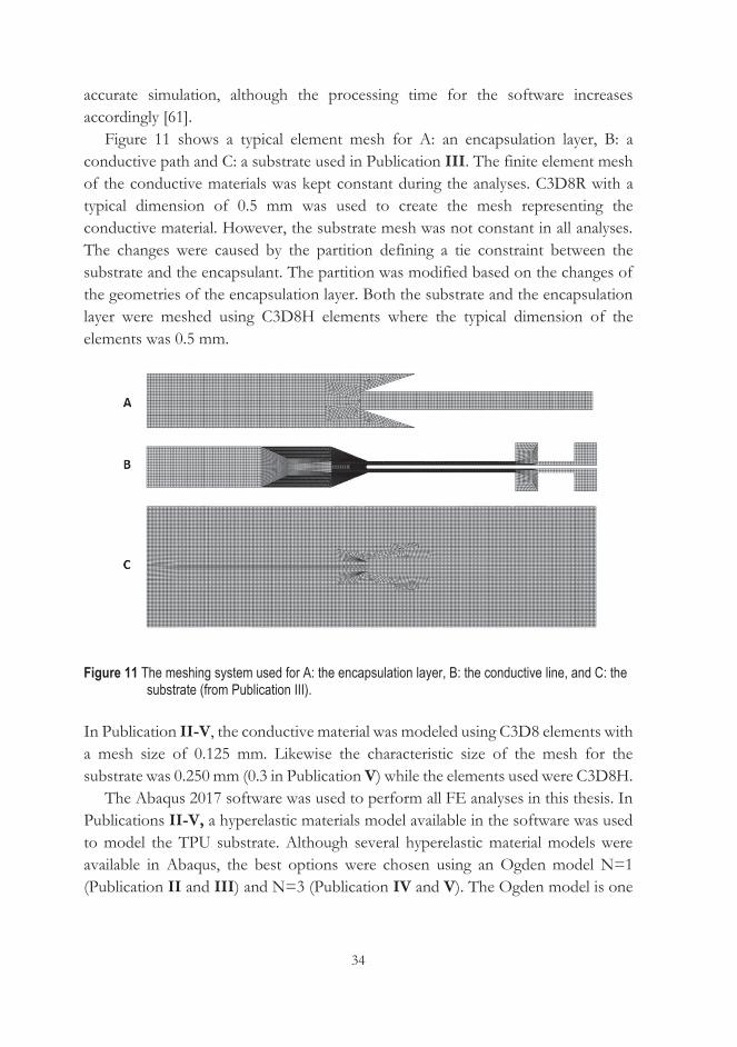
34
accurate simulation, although the processing time for the software increases accordingly [61].
Figure 11 shows a typical element mesh for A: an encapsulation layer, B: a conductive path and C: a substrate used in Publication III. The finite element mesh of the conductive materials was kept constant during the analyses. C3D8R with a typical dimension of 0.5 mm was used to create the mesh representing the conductive material. However, the substrate mesh was not constant in all analyses. The changes were caused by the partition defining a tie constraint between the substrate and the encapsulant. The partition was modified based on the changes of the geometries of the encapsulation layer. Both the substrate and the encapsulation layer were meshed using C3D8H elements where the typical dimension of the elements was 0.5 mm.
Figure 11 The meshing system used for A: the encapsulation layer, B: the conductive line, and C: the substrate (from Publication III).
In Publication II-V, the conductive material was modeled using C3D8 elements with a mesh size of 0.125 mm. Likewise the characteristic size of the mesh for the substrate was 0.250 mm (0.3 in Publication V) while the elements used were C3D8H.
The Abaqus 2017 software was used to perform all FE analyses in this thesis. In Publications II-V, a hyperelastic materials model available in the software was used to model the TPU substrate. Although several hyperelastic material models were available in Abaqus, the best options were chosen using an Ogden model N=1 (Publication II and III) and N=3 (Publication IV and V). The Ogden model is one

35
of the most common hyperelastic models to describe the non-linear stress-strain behaviour of polymers [136].
Figure 12 (A) compares the stress-strain data provided by the uniaxial test from Instron and the FE analyses results for the TPU substrate in Publication II where both the modeling and experimental results agreed well.
Figure 12 A: Modelling and experimental data for stress-strain behaviour of a pure TPU substrate. B-D represent the force-displacement behaviour of Patterns A-C respectively (from Publication II), ©2018 IEEE.
In systems including thin layers on the substrate, the derivation of the mechanical properties for the layers is challenging since the properties are different to the bulk materials [61]. There are however solutions such as nanoindentation to derive the mechanical properties of thin films [137].
The manufacturer of the conductive ink (ECM CI-1036) provided the Young’s Modulus and Poisson’s ratio values of 550 MPa and 0.035 respectively. Since these data were derived from dynamic mechanical analysis (DMA) testing, they were valid only for very small amount of deformation rates. As the strain value of stretchable interconnects made by this conductive material was much larger, the provided data from the manufacturer was not sufficient. Indeed, using DMA data in FE analyses

36
would provide overly stiff force-displacement curves for all layouts compared to the experimental data. On the other hand, it was not possible to determine the properties of the conductive material due to the small thickness and fragility of pure conductive film. Therefore, a series of experiments were performed to derive the properties of the conductive material through reverse engineering where analyses were performed while the properties were modified accordingly. In these experiments, the properties of the conductive material were obtained by uniaxial testing of the conductive film coated on a TPU substrate. The validity of material model was verified by a comparison of force-displacement curves of the samples with three different layouts. The applied material model for the conductive material included two regions: linear elastic and plastic. The Young’s modulus and Poisson’s ratio provided by the ink manufacturer were used for the initial part of the applied model, which was linear elastic. The elastic model was followed by a plastic region, which was used when reaching the yield stress. The first point was at a yield strength of 15 MPa and plastic strain of 0, while at the second point the stress was 80 MPa and the plastic strain was 0.01. Figure 12 (B-C) shows the modeling and experimental force-displacement of patterns A, B and C respectively.
In Publication IV, SMDs were rigid components whose mechanical stiffness were much higher in comparison to the other constituent components of the device. Therefore, SMDs were modelled as discrete rigid forms. Table 7 shows the properties of the substrate and conductive materials in the FE analyses of Publication IV and V.
Table 7 Properties of the substrate and conductive material used in the FE analysis (from Publication V, © IOP Publishing. Reproduced with permission. All rights reserved).
Properties of TPU Properties of conductive paste (GPa) 1.725
1 -4.725 1.402 0.3
2 1.392 3.295 Yield stress 1 (MPa) 19.67 at
3 9.196 -2.075
Yield stress 1 (MPa)
24.35 at

37
3 RESULTS AND DISCUSSION
Figure 13 is a flowchart summarizing the agenda of this thesis where the relevancy and findings of each publication are highlighted. The work is divided into two main sections. In the first section, the fabrication and characterization of stretchable interconnects were investigated. In the second section, the electromechanical performance and stretchability of the interconnects were improved by means of changes in the local stiffness of the substrate via three different approaches including the modification of the conductive line, addition of encapsulation, and removing material from the substrate. In all three approaches, the stiffness of the samples was locally modified to improve the stretchability of the devices.
Figure 13 A summary of the goals in the publication of this thesis and their correlations.

38
3.1 Fabrication and characterization of stretchable interconnects
In Publication I, the aims were the fabrication of stretchable interconnections and verification of methods for performing electromechanical characterization. Therefore, stretchable interconnects were fabricated using a screen-printing technique. Figure 14 illustrates the schematic of the design for the interconnects in Publication I.
Figure 14 U-shape design of the interconnects (from Publication I), © 2017 IEEE.
The stretchable interconnects were screen-printed on a 50 μm TPU-4201 substrate with dimensions of 38 mm × 110 mm using carbon ink (CI-2051). The left clamp was fixed while the right one stretched the sample. This is a simple U-shape design which is an especially beneficial layout to obtain the information about the materials and their stretchability. Carbon interconnects were characterized by measuring the results of a single pull-up test, a cyclic test, and their recovery after unloading (from a single-pull up test).
The initial values for the sheet resistance of samples were between 272 Ω/□ and 338 Ω/□ (36.2 mΩ/□ on average for similar sample fabricated using CI-1036 Ag-ink). Figure 15 shows the results of a single pull-up test with the corresponding SEM images from the relaxed state of the material, midway and after losing conductivity. Typical microcracks and their magnitude are highlighted in the photos.

39
Figure 15 The development of normalized resistance (R/R0) during the elongation (%) of stretchable carbon interconnects. The dashed line represents the electrical failure point. Inset images are SEM photos in a: relaxed, b: midway, initiation of cracks and c: full stretching before the failure point (scale bar: 10 μm), (from Publication I), © 2017 IEEE.
When the sample is relaxed, a uniform conductive film was formed. Upon loading, microcracks started to nucleate on the conductive film. The microcracks were propagated and enlarged as the stretching value increased. Finally, the cracks joined together, and it was no longer feasible for electrical charges to travel along the conductive film and loss of conductivity occurred. The SEM images helped to monitor the evolution of the microcracks on the conductive film. The durability of the interconnects was also characterized by repetitive loading/unloading for 1000 cycles with stretching values up to 40%, where devices could survive during all the cycles. Koivikko et.al. employed successfully the carbon stretchable interconnects developed in this work to fabricate soft actuators together with the silver ink used in the publication of this thesis [138].
3.2 Modification of conductive line
There is a frequent need for the interconnects to transform from a narrower structure to a wider format along stretchable electronic circuits such as on-skin applications, e.g. electronic tattoos. Therefore, in Publication II three geometries were designed to investigate the effects of different shapes of conductive paths for a narrow-to-wide transition. Figure 16 is a schematic of different layouts and the location of the clamps.
40
Figure 16 Schematic of three different structural layouts (Pattern A, B and C) (from Publication II), © 2018 IEEE.
Four contact pads were added to each set of designs to obtain four probe measurements if needed. These interconnects were screen-printed by using Ag-flake inks (CI-1036) as the conductive material on a TPU-4201 substrate.
The materials model explained earlier was used to simulate the loading conditions for all three layouts. Figure 17 shows the plastic strain (PE) corresponding to the displacement of 40% (20 mm) of each sample.
Figure 17 Plastic strain (PE) of 40% displacement for Patterns A, B and C (from Publication II) © 2018 IEEE.

41
As shown in the previous section, although the shape of the force-displacement curve in the both modeling and experimental data were close together (Figure 12), the distribution of the strain along the conductive paths were different. Indeed, the results of the plastic strain highlighted the differences between different layouts of the conductive material. Pattern B had the highest plastic strain value along the narrower conductive line. On the other hand, Pattern A had the least overall level of stain although the transition area on the narrower line had the maximum level of strain on the sample. For Pattern C, the maximum plastic strain existed in the sharp corners of the sample where they had a negligible effect on the conductivity of the device. For Patten C, the maximum plastic strain value on the conductive line was also slightly lower than for Pattern A. The modeling results suggested that Pattern C should have higher stretchability before failure compared to the other patterns. Therefore, the samples needed to be characterized in real life. Figure 18 (A) shows the comparison of the normalized resistances of each pattern in single pull-up tests. As it was shown in the modeling results, the lowest value for the plastic strain along the conductive line led the device to have higher stretchability compared to the other layouts. Likewise, Pattern A and B also followed the same trend as highlighted by the modeling. During the stretching for Pattern C, the stress first became concentrated in the sharp corners on the sides of layout and therefore the strain changed less along the conductive path. We called these corners as “sacrificial zones” since they adopt the maximum level of plastic strain before they let the strain transfer to the transition zone where the device is mostly prone to the failure. A batch of ten samples from each pattern were unidirectionally pulled up and the mean values of the stretchability for Pattern A-C were 44.25%, 41.45% and 54.32% respectively. Similarly, devices fabricated based on the three patterns went under repetitive loading/unloading for 1000 cycles at 20% stretching. Although all of them could survive all the cycles, Pattern C showed less growth in normalized resistance compared to the other patterns as shown in Figure 18 (B).

42
Figure 18 A: Comparison of the normalized resistances (R/R0) of typical samples from Pattern A, B and C, B in single pull-up test, : B: trend of normalized resistances for the first and last three cycles for each pattern (from Publication II) © 2018 IEEE.
Since conductive materials are relatively more expensive compared, e.g., to dielectrics, the authors suggest using cheaper materials in the sacrificial zones in mass production in order to reduce the overall production cost.
SEM images were taken from a fresh sample and from one that experienced 1000 cycles (both samples were adapted from Pattern C). Images for both samples were taken when they were unloaded. Figure 19 (A) shows the fresh sample, whereas Figure 19 (B) shows a sample that underwent the cyclic test. As it can be seen, the density of microcracks increased after the cyclic test. The white arrows emphasize some random microcracks on the surface of the conductive path. Subsequently, the charges were not able to move through the conductive path as they could in the fresh sample due to the presence of microcracks, and the resistance increased accordingly. Figure 19 (C) shows an SEM image of the cross-section of a fresh device where the area of interest is magnified in the right side of the image. In this image, the black zone is the TPU substrate and Pt layer as the protection layer is extended on the top.

43
Figure 19 An FESEM image of the surface of the conductive track on the TPU substrate in its un-stretched form for A: a fresh sample, B: a sample after 1000 cycles and C: an FIBSEM image of the cross section of the conductive track on the TPU substrate (from Publication II), © 2018 IEEE.
Between the TPU substrate and Pt protection layer, silver flakes are shown in gray where each individual flake forms larger rods. These conductive rods joined together and provided the electrical conductivity along the conductive path. It is worth noting that the concept of the sacrificial zone was demonstrated to work also in the case of SMD components pads on printed circuit [139].
3.3 Modification of local stiffness by adding encapsulation
While in Publication II, the effects of the geometry of conductive materials were studied for a narrow-to-wide transition during the stretching, in Publication III the effect of the encapsulation materials and their geometries on the transition were investigated. For this aim, Pattern B was selected from Publication II as it required less conductive material for fabrication (which is especially important in mass production). Two layouts for the encapsulation materials were studied, a full and partial encapsulation of the sample, together with a non-encapsulated sample, as illustrated in Figure 20.

44
Figure 20 Schematic illustration of stretchable interconnects. A: a non-encapsulated sample, B: an entirely encapsulated sample, C: a partially encapsulated sample (from Publication III).
The stretchable interconnects were initially fabricated using a screen-printing technique. Silver ink (ECM CI-1036) and TPU-4201 were used as the conductive material and substrate materials accordingly. In addition, heat-laminated TPU film (the same as the substrate) and a UV-curable dielectric ink (ECM DI-7540) were used as encapsulation materials.
FE analyses were performed to optimize the geometry of the encapsulation when it partially coated the sample. While the geometries of substrate and conductive track were kept constant, the geometry of encapsulation layer was modified. Solid elements were used to create an FE model and all components (the substrate, conductive materials and TPU encapsulation layer) were modeled as separate parts. As shown in Figure 20 (C), three parameters (X, Y and Z) were modified via the FE analyses, while the failure of the conductive path was introduced. This failure was the point the elements were no longer able to maintain a continuous path, as shown in Figure 21. The discontinued parts represent the area where elements crossed the critical plastic strain and they were removed for visualization purposes. The modified geometry of the TPU encapsulation layer was selected after analyses of 23 geometries. The range of failure strain for these 23 cases were between 50% to almost 60%. The modified value for the three parameters of the TPU encapsulation layer were 2 mm, 25 mm and 5 mm for X, Y and Z, respectively. The entirely TPU-
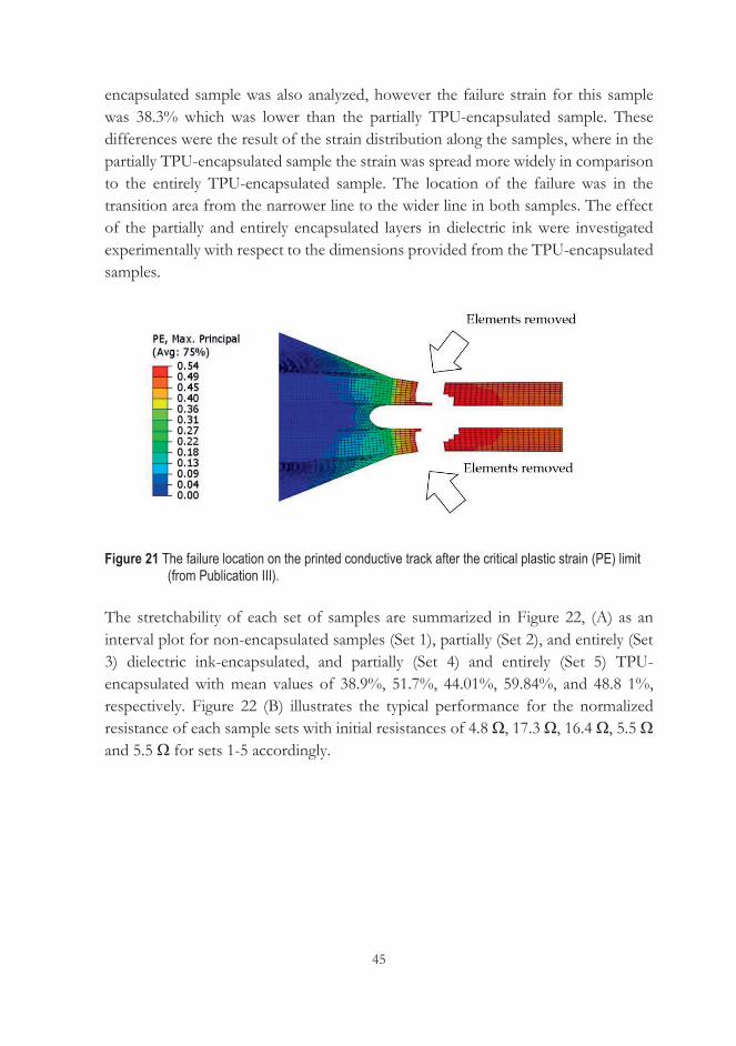
45
encapsulated sample was also analyzed, however the failure strain for this sample was 38.3% which was lower than the partially TPU-encapsulated sample. These differences were the result of the strain distribution along the samples, where in the partially TPU-encapsulated sample the strain was spread more widely in comparison to the entirely TPU-encapsulated sample. The location of the failure was in the transition area from the narrower line to the wider line in both samples. The effect of the partially and entirely encapsulated layers in dielectric ink were investigated experimentally with respect to the dimensions provided from the TPU-encapsulated samples.
Figure 21 The failure location on the printed conductive track after the critical plastic strain (PE) limit (from Publication III).
The stretchability of each set of samples are summarized in Figure 22, (A) as an interval plot for non-encapsulated samples (Set 1), partially (Set 2), and entirely (Set 3) dielectric ink-encapsulated, and partially (Set 4) and entirely (Set 5) TPU-encapsulated with mean values of 38.9%, 51.7%, 44.01%, 59.84%, and 48.8 1%, respectively. Figure 22 (B) illustrates the typical performance for the normalized resistance of each sample sets with initial resistances of 4.8 Ω, 17.3 Ω, 16.4 Ω, 5.5 Ω and 5.5 Ω for sets 1-5 accordingly.

46
Figure 22 A summary of the stretchability preference of interconnects. A: an interval plot of the stretchability of different sets of samples, 1: non-encapsulated, 2: partially ink-encapsulated, 3: entirely ink-encapsulated, 4: partially TPU-encapsulated and 5: entirely TPU-encapsulated, B: typical performance for normalized resistance of each sample set (from Publication III).
As stated in various works such as [14], [140]–[143], the encapsulation of interconnects and functional components provides mechanical and environmental support for the devices and hence improves their reliability. Generally, the encapsulation of interconnects delays crack formation and propagation on the conductive path. This phenomenon was observed in the results of the single pull-up tests in this study as the average stretchability of the encapsulated samples with TPU-encapsulation layer and UV-curable ink (either partially or entirely covered) were higher compared to non-encapsulated ones. In addition, the normalized resistances of all the encapsulated samples increased more gently than the non-encapsulated samples during the single-pull up test. On the other hand, partially encapsulated samples could stretch more than their entirely encapsulated counterparts. This can be explained by the effect of local increases in the stiffness. Therefore, when the sample was stretched, non-encapsulated areas released the strain earlier and less strain was directed to the encapsulated area (where it had higher local stiffness). The concept of sacrificial edges developed in Publication II was used to shield the transition area.
Cyclic tests were also conducted for samples for 10000 cycles at stretching values of 10% and 20%. The samples encapsulated by the UV-curable dielectric performed weakly compared to the others. The weak adhesion strength between the dielectric ink and the substrate did not provide protective support for the conductive path against the cyclic test. In addition, UV-exposure during the curing process of the dielectric ink, caused a mechanical degradation of the substrate, which led to a reduction of the mechanical properties of the TPU substrate and weakened the
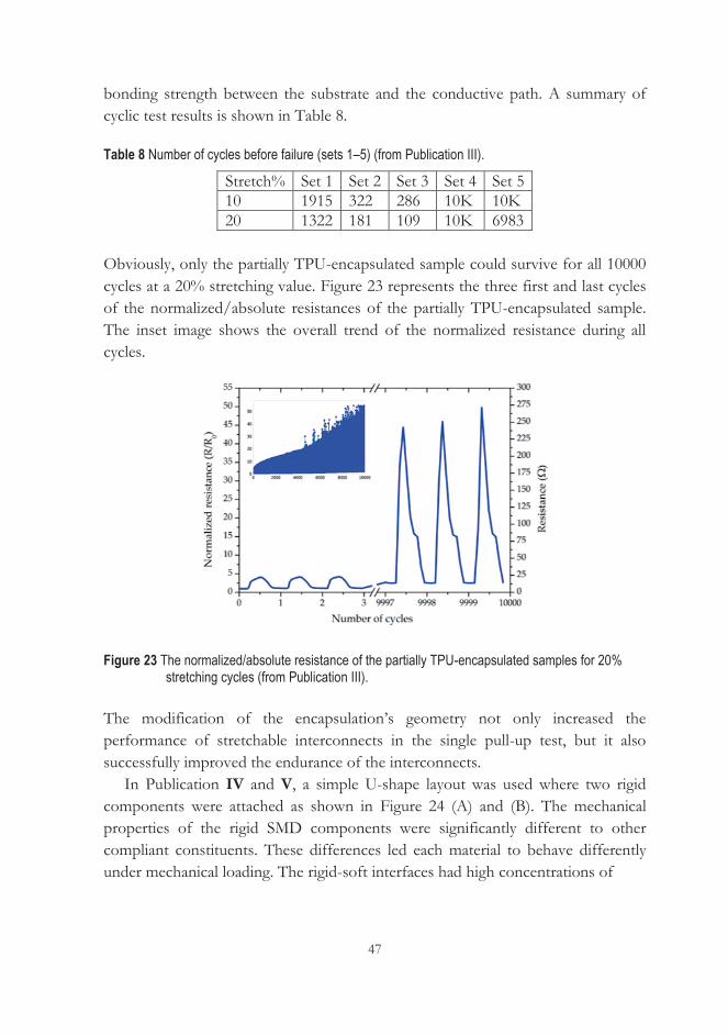
47
bonding strength between the substrate and the conductive path. A summary of cyclic test results is shown in Table 8.
Table 8 Number of cycles before failure (sets 1–5) (from Publication III).
Stretch% Set 1 Set 2 Set 3 Set 4 Set 5 10 1915 322 286 10K 10K 20 1322 181 109 10K 6983
Obviously, only the partially TPU-encapsulated sample could survive for all 10000 cycles at a 20% stretching value. Figure 23 represents the three first and last cycles of the normalized/absolute resistances of the partially TPU-encapsulated sample. The inset image shows the overall trend of the normalized resistance during all cycles.
Figure 23 The normalized/absolute resistance of the partially TPU-encapsulated samples for 20% stretching cycles (from Publication III).
The modification of the encapsulation’s geometry not only increased the performance of stretchable interconnects in the single pull-up test, but it also successfully improved the endurance of the interconnects.
In Publication IV and V, a simple U-shape layout was used where two rigid components were attached as shown in Figure 24 (A) and (B). The mechanical properties of the rigid SMD components were significantly different to other compliant constituents. These differences led each material to behave differently under mechanical loading. The rigid-soft interfaces had high concentrations of

48
Figure 24 The schematic of layouts for stretchable interconnects used in this thesis (from Publication IV and Publication V, right part: © IOP Publishing. Reproduced with permission. All rights reserved).
stress-strain when the system was stretched. These interfaces are prone as the starting location of a failure. The rigid-soft interfaces needed to be protected, so the idea of local stiffness from Publication III inspired Publications IV and V. Likewise, in Publications IV and V two approaches to improve the electromechanical performance of stretchable interconnects with two SMD components were investigated. Stretchable interconnects were fabricated in a similar way to the methods used in Publications II and III. Then two SMD 2512 components with physical dimensions of 6.3 mm × 3.2 mm from TopLine Corporation were bonded with the ICA using a digital automatic dispenser. The island-bridge configuration was used in the design of the stretchable interconnects.
In Publication IV, vulnerable regions in the substrate (areas with soft-rigid interfaces) were reinforced by locally increasing the stiffness. For this aim, two layouts were designed where the TPU-encapsulation material was heat laminated onto the substrate. In Design 1, two straps of TPU were heat laminated on the conductive track in areas including SMD components, while in Design 2 three straps of TPU were encapsulated on the sides of the conductive track including the SMD components. In the other approach, the local stiffness of areas including soft-rigid interfaces were increased by removing materials from substrate away from the soft-rigid interfaces. More precisely, increasing the local stiffness in a reverse way than in Designs 1 and 2.

49
The mechanical behaviour of the samples was initially investigated using the Abaqus software and then samples were fabricated and characterized accordingly. In the FE analyses, the samples were unidirectionally stretched up to a nominal strain of 0.4.
Figure 25 A: Details of the deformed shapes for the different designs next to the SMD components; the entity plotted is the true strain in the X-direction, which is coaxial with the loading direction, B: Plot of the true strain along the X-direction via the conductive wire, starting from conductive track next to the SMD (from Publication IV).
Figure 25 (A) represents the true strain on the deformation field in the vicinity of SMD components. As it can be seen, the maximum level of strain is different in the samples depending on their geometries. Figure 25 (B) shows the strain development along the conductive track to specify the influences of the modifications on them where the electromechanical failure is expected to happen. The maximum peak for the strain existed next to the SMD component in the reference since there was not any kind of shielding in this sample. In the other samples similar peaks were shown in this area however the magnitude of the strains was mitigated due to the positive effect of the design modifications. In Design 1, the maximum level of deformation occurred at 11 mm away from the beginning of the track where the TPU straps ended. This was the effect of the stiffener under the conductive track and similarly a sudden jump in the strain level happened at the edge of TPU strap where it was not continued anymore due to the local strain amplification in the conductive track direction. On the other hand, the deformation levels in Design 2 and Design 3 had a slower slope in this region. More precisely, in Design 3, the deformation peak was reached roughly 16 mm away from the SMD component where material from substrate was removed. In Design 2, the maximum level of deformation decreased

50
due to the effect of TPU straps on the sides of the SMD components. Indeed, the design allowed for a smoother change in deformation along the conductive track. The location of the TPU straps played the main role in the different behaviours for Design 1 and 2 since the creation of interfaces under the track in Design 1, could increase the strain concentration along the conductive track while in Design 2 local stiffening of the sample on the sides of SMD components, provided a smoother distribution of the strain on the conductive path and avoided excessive deformation.
A batch of 10 samples from the reference and other modified samples were experimentally characterized with a single-pull up test until the electrical failure point. Figure 26 (A), a typical stretchability of one sample from each category is shown.
Figure 26 A: Normalized resistance (R/R0) of typical samples from different designs in a single pull-up test, B: box and whiskers plot for the stretchability of different samples (from Publication IV).
In Figure 26 (B), the average stretchability before failure for all designs is illustrated in a box and whiskers graph. The mean value for the stretch ratio of the reference and Designs 1-3 are: 1.240, 1.27, 1.42 and 1.35 (equal to a nominal strain of 0.24, 0.27, 0.42 and 0.35) respectively. These results agreed well with the results obtained from the FE analyses. The results from both the FE analyses and experimental data proved that stiffening the regions in the vicinity of the SMD components could improve the behaviour of samples under deformation since local stiffening leads to the formation of strain concentrations in other regions away from rigid-soft interfaces and improves the distribution of the strain especially in the interfaces. In Design 3, an improvement in electromechanical performance was achieved without the application of an encapsulation layer. This would make the approach superior to the rest since the electromechanical behaviour is independent of the encapsulation

51
quality. In addition, this approach bypasses the extra encapsulation stage which is beneficial from both environmental and economic perspectives in large area production.
3.4 Modification of local stiffness by removing material
In Publication V, we continued to investigate the idea of increasing the local stiffness in the vicinity of rigid-soft interfaces by partially removing material from the substrate. More specifically, material from the substrate away from the SMD components in shape of small circles with desired arrangements were removed precisely with a laser cutting machine (Trotec Speedy 100). Unlike shapes such as ovals, squares, rectangles, semicircles, etc., a circle is a symmetrical shape that is defined by one parameter (its radius). Therefore, in case the device needs to be deformed on a different axis, a circle offers the same property. It is also less complicated to have limited parameters in the modeling. In different structure such as laminated composites, it is often needed to drill to pass communication lines, pipes, etc. Since these holes create stress concentrations, one way to reduce the concentration of stress around the holes is to create auxiliary circular holes around the main hole [144]–[146]. Likewise, we decided to employ this idea (a circular shape) to remove the material, tune the stiffness and shift the stress and strain concentration to less critical regions. In this way, two sets of design were suggested where the shape of the removed material, density, arrangement, and distance from them to the conductive track were studied.

52
Figure 27 A: The FE analyses for the true strain at the maximum location of deformation for different samples (at a strain of 0.4). B and C: progress of the true strain on the conductive track from near the SMD (highlighted by yellow lines) for Set A and Set B respectively (at a strain of 0.4), D: DIC analyses of the strain field for different samples sets. E: development of the stain on the silver tracks in different sample sets (from Publication V, © IOP Publishing. Reproduced with permission. All rights reserved).
Figure 27 (A-C) represents the result of FE analyses for the samples. In the analyses, models were uniaxially loaded up to nominal strain of 0.4. In Figure 27 (A), the plots indicating the true strain at the maximum displacement subjected to the samples so it can be determined how the deformation levels on the conductive track were different. These differences arose from the vicinity of the materials removed to the conductive track. On the other hand, although the amount of removed material was almost similar (44 mm2 for the Set A and 46 mm2 for the set B), the feature sizes could influence the deformation quality. Figure 27 (B, C) highlights different behaviour for different feature sizes of removed materials. If the geometrical features were too small (e.g., shapes smaller than 0.5 mm in radius), they would not effectively influence the deformation behaviour of the conductive track.
Figure 27 (D, E) shows DIC analyses for all sample sets and the results indicated a good agreement with the results of the FE analyses. In Figure 27 (D), the development of strain fields is shown while Figure 27 (E) quantitatively compares the strains along the conductive track (from the SMD). These results indicate how

53
the peak of the deformation varies between different sets of samples. More precisely, in the reference sample and Set B, the maximum value of strain existed near the SMD-conductive track edges. In Set A however the strain concentration had the highest values away from the SMD-conductive track and next to the circular holes where three peaks of strain emerged. The electromechanical failure for each sample set was expected to occur at the points with the maximum strain concentrations.
Figure 28 A: A summary of stretchability plotted for 10 samples for different samples sets, B: Schematic illustration of cross section of a sample in the SMD area, C and D: an SEM image of a fresh sample and one with 1000 cycles at 20% (debonding of ICA from the conductive track is highlighted) (from Publication V, © IOP Publishing. Reproduced with permission. All rights reserved).
Figure 28 (A) summarizes the result of the single-pull up test for each set of samples (10 samples per set). Both modified samples performed better compared to the reference sample. While Set A and Set B had average stretchability with a normal strain of 0.36 and 0.44, this value was 0.25 for the refence sample. In fact, the presence of SMD components in the reference sample induced the strain localization in this area where the homogenous distribution of deformation throughout the sample was prevented. As a result, microcrack nucleation started from this area where the concentration of the strain in the polymeric binder of the conductive path extended beyond the yield point during the loading of the sample and emerging higher density of microcracks occurred to release the strain against larger deformation rates. The steady growth of microcracks continued upon further stretching until the formation of major fractures in the conductive path and the

54
electromechanical failure of the sample. In sample Set A and Set B, removing materials in the regions away from the SMD components lowered the stiffness in this area. On the other hand, this approach would increase the local stiffness in regions around the SMD components and hence reduced the strain concentration in the area accordingly. Moreover, circles were discontinuities on substrate that caused strain concentration. However, they were deliberately introduced to direct the strain concentration away from the conductive path, so the electrical conductivity was not affected. Although locally tuning the stiffness successfully mitigated the strain concentration throughput the sample, this approach cannot eliminate it entirely. In sample Set B, the distribution of the strain was more homogenous though.
During the cyclic test (with a maximum strain of 0.2), the reference sample, Set A and Set B could survive for 105, 173, and 227 cycles, respectively. When the samples underwent frequent loading/unloading cycles, the microcracks that nucleated on the stiffer material (conductive track) could grow and join each other. However, debonding occurred in the interfacial layers in fatigue tests. Figure 28 (B) represents a schematic of the cross section of the device highlighting the interfaces between different components. Figure 28 (C) shows an SEM image of a fresh sample and Figure 28 (D) illustrates an SEM image of a sample that went under 1000 cycles at a strain of 0.2 (both samples were relaxed during the SEM imaging). Although the bonding between the SMD component and ICA remained intact in both samples, the interface between the ICA and conductive lines was deformed for the non-fresh sample and ICA slipped and debonded from the conductive line. The mechanical mismatching properties created stress on the interface and because of poor adhesion, debonding between the ICA and conductive path occurred. This happened for all samples although the intensity was greater for the reference sample. Debonding of the ICA from the conductive path is marked in Figure 28 (D).
Creep and relaxation tests were also conducted for all samples to simulate the real-life conditions of the devices under persistent loading condition. During the creep test, it was found that modified samples could deform more at a fixed level of force in comparison to the reference sample. This is especially beneficial in wearable applications where users pay less attention to the applications when they are worn and hence the unobtrusiveness of the application would increase.

55
4 CONCLUSION
Stretchable electronics open a window toward the development of applications where mechanical deformability can improve the functionality and reliability of devices. It would be easier and more comfortable for a patient to wear a stretchable healthcare monitoring device if they were compatible with the movement of the user. This comfortability is not only beneficial in the long-term monitoring of the patient but also improves the reliability of the collected data since the patient pays less attention to the device compared to conventional rigid counterparts. Printing is a promising approach for the fabrication of stretchable electronics, although fully printed circuits still suffer from a low integration density, minimum feature size and slow response time compared to silicon-based devices. A heterogenous system is a strong candidate to combine the advantages of conventional and stretchable printed electronics. For this aim different components are integrated into a single device. Based on this concept miniaturized rigid components as small islands can be bridged together by stretchable interconnects to create a stretchable system. Although this is a promising approach for the fabrication of stretchable electronics, several challenges such as large derivations in the Young’s modulus and coefficient of thermal expansion of the different constituent materials, as well as fabrication and characterization methods need to be addressed and improved.
The proposed approaches in this thesis, give easily adaptable and cost-effective strategies to design and fabricate stretchable electronics for wearable electronics. Likewise, the practical ways to improve the electromechanical reliability of the stretchable devices were studied. It was shown that regardless of the electrical design, the reliability of the system can be enhanced by means of change in the mechanical properties. Initially a new concept of “sacrificial zones” was developed which can mitigate the concentration of stress in vulnerable areas (e.g., dimensional changes along the interconnects). Then the stiffness of the substrate was tuned by means of adding/removing materials from the substrate in order to protect the rigid-soft interfaces. In all the publications of this thesis, the aim to achieve at least 20% stretchability for the fabricated devices was achieved. A summary of this thesis is as the followings:

56
In Publication I stretchable carbon interconnects were fabricated and characterized. The verification of the characterization methods was the main objective of this work and this was reflecting in the other works of this thesis.
Publication II presented different ways to change the dimensions of the conductive track along the stretchable interconnects. More specifically three layouts were introduced to accommodate a narrow-to-wide transition by changing the design of the conductive materials. FE analyses were implemented by defining the physical properties of the substrate and conductive material in order to virtually investigate the behaviour of samples under deformation. So-called “sacrificial zones” were employed in one of the layouts to act as the protective shields on the sides of the interconnects where the dimensional change happened. When the interconnects were stretched, the stress was initially concentrated in the sacrificial zones which had no influence on the electrical performance of the device. Stretchable interconnects fabricated based on this layout presented a higher stretchability of 10% and 13% on average compared to two other layouts. Since the modification is done by changing the format of the conductive track instead of adding an encapsulation layer, the devices are more flexible and hence more comfortable for the user when they are implemented in wearable applications.
In Publication III, the electromechanical properties of the stretchable interconnects were improved by the addition of an encapsulation layer. Here two layouts for the encapsulation materials were used which either entirely or partially encapsulated the device. The layout of the partially-encapsulated interconnects included the “sacrificial zones” inspired by the work in Publication II. Although devices prepared with either a partial or entirely encapsulation layer performed better than the reference device (with no extra encapsulation layer), the partially-encapsulated device had better mechanical properties. This was justified by the effect of a local increase of stiffness on the conductive line, where the non-encapsulated area could release the strain earlier to relieve the stress. Hence, the higher stretchability of the device was achieved. Unlike in Publication II, the sacrificial zones were achieved by means of encapsulation layers rather than the conductive material. This would reduce the use of conductive material, which is more expensive than the encapsulation material. However, the encapsulation process needs to be done precisely to avoid delamination during moments of deformation.
Publication IV employed a simple U-shape interconnect including two SMD components and the aim was to improve the stretchability of the system. The concept of sacrificial zones was not applicable in this work because of the presence of rigid components. However, the idea of locally tuning the substrate was again

57
employed with the application of the encapsulation layer. The presence of SMD components created a rigid-soft interface with a high level of strain concentration and hence early failure of the device. To homogenize the strain field along the conductive track, the sides of the components were partially encapsulated. The partial encapsulation increased the local stiffness of the device in the vicinity of the SMD components and thus avoided the strain concentrations near the components. The results of simulations from the FE analyses and the practical data agreed well together.
Publication V continued the work in Publication IV by means of increasing the local stiffness in the opposite way. For this aim two sets of samples were designed by partially removing the substrate in areas far away from the rigid components. Both modified samples presented better electromechanical properties under different loading conditions, i.e., in single pull-up, cyclic loading, creep and stress relaxation tests. The FE analyses and experimental data confirmed that not only removing the material but also the shape and density of the removal materials could affect the strain distribution in the samples. Protection of the rigid-soft interface in Publication IV was done by encapsulation which requires an extra stage in the fabrication line which is not economically and environmentally beneficial. Moreover, the properties of the encapsulation material and the adhesion strength between the encapsulant and the underlayer can directly affect the functionality of the device. Tuning the stiffness by removing the material not only bypasses the encapsulation stage but also solves the aforementioned issues.
In conclusion, stretchable electronics add a number of features in potential applications such as health care monitoring systems compared to conventional rigid devices, including lower weight, cheaper price, mechanical deformability, design freedom and ease of use. Despite the progresses in the field of stretchable electronics there are still challenges in the development of new materials to facilitate deformability and reliability that need to be addressed. Moreover, as in most of current stretchable electronic packages, there are still a number of miniaturized rigid units, and engineered structural designs are needed to release the subjected stress on the interconnects and minimize the strain concentration in the rigid-soft locations. From the fabrication point of view, printing methods seem to be a promising way to develop stretchable electronics in both research and commercialization because of the scalability, cheaper manufacturing cost, and possibility to print on a variety of substrates. However, these methods still need further improvement, especially when a high resolution is required in mass production. For the future work of this thesis, the fabrication of a set-up to facilitate the stretching of devices in different directions

58
(e.g., biaxial, omnidirectional) needs to be investigated. In addition, the influence of environmental parameters such as temperature and humidity on the functionality of the devices should be studied. These parameters can especially influence the bonding strength between rigid components and substrates. As it was mentioned earlier, a possible application for stretchable interconnects are stretchable skin sensors and textile applications, and therefore, the effect of chemicals such as sweat, and detergents are also important to consider in future studies.

59
REFERENCES
[1] N. Matsuhisa, X. Chen, Z. Bao, and T. Someya, “Materials and structural designs of stretchable conductors,” Chem. Soc. Rev., vol. 48, no. 11, pp. 2946–2966, 2019.
[2] S. Khan, S. Ali, and A. Bermak, “Recent Developments in Printing Flexible and Wearable Sensing Electronics for Healthcare Applications,” Sensors, vol. 19, no. 5, p. 1230, Mar. 2019.
[3] Y. Gu et al., “Mini Review on Flexible and Wearable Electronics for Monitoring Human Health Information,” Nanoscale Res. Lett., vol. 14, no. 1, p. 263, Dec. 2019.
[4] H. Yousef, M. Boukallel, and K. Althoefer, “Tactile sensing for dexterous in-hand manipulation in robotics—A review,” Sensors Actuators A Phys., vol. 167, no. 2, pp. 171–187, Jun. 2011.
[5] K. Suganuma, Introduction to Printed Electronics, vol. 74. New York, NY: Springer New York, 2014.
[6] J. Chang, X. Zhang, T. Ge, and J. Zhou, “Fully printed electronics on flexible substrates: High gain amplifiers and DAC,” Org. Electron., vol. 15, no. 3, pp. 701–710, Mar. 2014.
[7] W. S. Wong and A. Salleo, Eds., Flexible Electronics, vol. 11. Boston, MA: Springer US, 2009.
[8] L.-R. Zheng, H. Tenhunen, and Z. Zou, Smart Electronic Systems. Weinheim, Germany: Wiley-VCH Verlag GmbH & Co. KGaA, 2018.
[9] L. Xie, “Heterogeneous integration of silicon and printed electronics for intelligente sensing devices,” Information and Communication Technology, KTH Royal Institute of Technology, 2014.
[10] “Heterogeneous Integration Roadmap - IEEE Electronics Packaging

60
Society.” [Online]. Available: https://eps.ieee.org/technology/heterogeneous-integration-roadmap.html. [Accessed: 24-Apr-2020].
[11] S. Nagels and W. Deferme, “Fabrication Approaches to Interconnect Based Devices for Stretchable Electronics: A Review,” Materials (Basel)., vol. 11, no. 3, p. 375, Mar. 2018.
[12] H. Hocheng and C.-M. Chen, “Design, Fabrication and Failure Analysis of Stretchable Electrical Routings,” Sensors, vol. 14, pp. 11855–11877, 2014.
[13] M. D. Dickey, “Stretchable and Soft Electronics using Liquid Metals,” Adv. Mater., vol. 29, no. 27, p. 1606425, Jul. 2017.
[14] W. Wu, “Stretchable electronics: functional materials, fabrication strategies and applications,” Sci. Technol. Adv. Mater., vol. 20, no. 1, pp. 187–224, Dec. 2019.
[15] F. Bossuyt, T. Vervust, and J. Vanfleteren, “Stretchable Electronics Technology for Large Area Applications: Fabrication and Mechanical Characterization,” IEEE Trans. Components, Packag. Manuf. Technol., vol. 3, no. 2, pp. 229–235, Feb. 2013.
[16] K. Li et al., “A Generic Soft Encapsulation Strategy for Stretchable Electronics,” Adv. Funct. Mater., vol. 29, no. 8, p. 1806630, Feb. 2019.
[17] X. Yu, B. Mahajan, W. Shou, and H. Pan, “Materials, Mechanics, and Patterning Techniques for Elastomer-Based Stretchable Conductors,” Micromachines, vol. 8, no. 1, p. 7, Dec. 2016.
[18] D.-H. Kim, J. Xiao, J. Song, Y. Huang, and J. A. Rogers, “Stretchable, Curvilinear Electronics Based on Inorganic Materials,” Adv. Mater., vol. 22, no. 19, pp. 2108–2124, Jan. 2010.
[19] S.-M. Yi, I.-S. Choi, B.-J. Kim, and Y.-C. Joo, “Reliability Issues and Solutions in Flexible Electronics Under Mechanical Fatigue,” Electron. Mater. Lett., vol. 14, no. 4, pp. 387–404, Jul. 2018.
[20] J. Suikkola et al., “Screen-Printing Fabrication and Characterization of Stretchable Electronics,” Sci. Rep., vol. 6, p. 25784, May 2016.

61
[21] Y. Zhao and X. Huang, “Mechanisms and Materials of Flexible and Stretchable Skin Sensors,” Micromachines, vol. 8, no. 3, p. 69, Feb. 2017.
[22] D. F. Fernandes, C. Majidi, and M. Tavakoli, “Digitally printed stretchable electronics: a review,” J. Mater. Chem. C, vol. 7, no. 45, pp. 14035–14068, 2019.
[23] F. Stauffer et al., “Skin Conformal Polymer Electrodes for Clinical ECG and EEG Recordings,” Adv. Healthc. Mater., vol. 7, no. 7, p. 1700994, Apr. 2018.
[24] S. R. Madhvapathy et al., “Epidermal Electronic Systems for Measuring the Thermal Properties of Human Skin at Depths of up to Several Millimeters,” Adv. Funct. Mater., vol. 28, no. 34, p. 1802083, Aug. 2018.
[25] J. Choi, R. Ghaffari, L. B. Baker, and J. A. Rogers, “Skin-interfaced systems for sweat collection and analytics,” Sci. Adv., vol. 4, no. 2, p. eaar3921, Feb. 2018.
[26] O. H. Huttunen, T. Happonen, J. Hiitola-Keinänen, P. Korhonen, J. Ollila, and J. Hiltunen, “Roll-To-Roll Screen-Printed Silver Conductors on a Polydimethyl Siloxane Substrate for Stretchable Electronics,” Ind. Eng. Chem. Res., vol. 58, no. 43, pp. 19909–19916, Oct. 2019.
[27] W. Dang, V. Vinciguerra, L. Lorenzelli, and R. Dahiya, “Printable stretchable interconnects,” Flex. Print. Electron., vol. 2, no. 1, p. 013003, Mar. 2017.
[28] T. Yoshikai, H. Fukushima, M. Hayashi, and M. Inaba, “Development of soft stretchable knit sensor for humanoids’ whole-body tactile sensibility,” in 2009 9th IEEE-RAS International Conference on Humanoid Robots, 2009, pp. 624–631.
[29] S. Hong, S. Lee, and D.-H. Kim, “Materials and Design Strategies of Stretchable Electrodes for Electronic Skin and its Applications,” Proc. IEEE, vol. 107, no. 10, pp. 2185–2197, Oct. 2019.
[30] T. Someya, Ed., Stretchable Electronics. Weinheim, Germany: Wiley-VCH Verlag GmbH & Co. KGaA, 2012.
[31] M. A. Yokus, R. Foote, and J. S. Jur, “Printed Stretchable Interconnects

62
for Smart Garments: Design, Fabrication, and Characterization,” IEEE Sens. J., vol. 16, no. 22, pp. 7967–7976, Nov. 2016.
[32] J. Kim et al., “Stretchable silicon nanoribbon electronics for skin prosthesis,” Nat. Commun., vol. 5, no. 1, p. 5747, Dec. 2014.
[33] R. C. Webb et al., “Ultrathin conformal devices for precise and continuous thermal characterization of human skin,” Nat. Mater., vol. 12, no. 10, pp. 938–944, Oct. 2013.
[34] T. Yamada et al., “A stretchable carbon nanotube strain sensor for human-motion detection,” Nat. Nanotechnol., vol. 6, no. 5, pp. 296–301, May 2011.
[35] X. Huang et al., “Stretchable, Wireless Sensors and Functional Substrates for Epidermal Characterization of Sweat,” Small, vol. 10, no. 15, pp. 3083–3090, Aug. 2014.
[36] S.-I. Park et al., “Printed Assemblies of Inorganic Light-Emitting Diodes for Deformable and Semitransparent Displays,” Science (80-. )., vol. 325, no. 5943, pp. 977–981, Aug. 2009.
[37] S. Xu et al., “Soft Microfluidic Assemblies of Sensors, Circuits, and Radios for the Skin,” Science (80-. )., vol. 344, no. 6179, pp. 70–74, Apr. 2014.
[38] T. Sekitani, Y. Noguchi, K. Hata, T. Fukushima, T. Aida, and T. Someya, “A Rubberlike Stretchable Active Matrix Using Elastic Conductors,” Science (80-. )., vol. 321, no. 5895, pp. 1468–1472, Sep. 2008.
[39] D.-H. Kim et al., “Materials for multifunctional balloon catheters with capabilities in cardiac electrophysiological mapping and ablation therapy,” Nat. Mater., vol. 10, no. 4, pp. 316–323, Apr. 2011.
[40] M. ÇİÇEK, “WEARABLE TECHNOLOGIES AND ITS FUTURE APPLICATIONS,” Int. J. Electr. Electron. Data Commun., vol. 3, no. 4, pp. 45–50, 2015.
[41] T. Vuorinen et al., “Validation of Printed, Skin‐Mounted Multilead Electrode for ECG Measurements,” Adv. Mater. Technol., vol. 4, no. 9, p. 1900246, Sep. 2019.
[42] B. Huyghe, H. Rogier, J. Vanfleteren, and F. Axisa, “Design and

63
Manufacturing of Stretchable High-Frequency Interconnects,” IEEE Trans. Adv. Packag., vol. 31, no. 4, pp. 802–808, Nov. 2008.
[43] P. Rosa, A. Câmara, and C. Gouveia, “The Potential of Printed Electronics and Personal Fabrication in Driving the Internet of Things,” Open J. Internet Things, vol. 1, no. 1, pp. 16–36, 2015.
[44] T. Cheng, Y. Zhang, W.-Y. Lai, and W. Huang, “Stretchable Thin-Film Electrodes for Flexible Electronics with High Deformability and Stretchability,” Adv. Mater., vol. 27, no. 22, pp. 3349–3376, Jun. 2015.
[45] J. A. Rogers, “Materials for semiconductor devices that can bend, fold, twist, and stretch,” MRS Bull., vol. 39, no. 06, pp. 549–556, Jun. 2014.
[46] Y. Zhang et al., “Mechanics of ultra-stretchable self-similar serpentine interconnects,” Acta Mater., vol. 61, no. 20, pp. 7816–7827, Dec. 2013.
[47] R. J. D. Tilley, Understanding Solids. Chichester, UK: John Wiley & Sons, Ltd, 2004.
[48] S. J. Benight, C. Wang, J. B. H. Tok, and Z. Bao, “Stretchable and self-healing polymers and devices for electronic skin,” Prog. Polym. Sci., vol. 38, no. 12, pp. 1961–1977, Dec. 2013.
[49] W. Zeng, L. Shu, Q. Li, S. Chen, F. Wang, and X.-M. Tao, “Fiber-Based Wearable Electronics: A Review of Materials, Fabrication, Devices, and Applications,” Adv. Mater., vol. 26, no. 31, pp. 5310–5336, Aug. 2014.
[50] J.-S. Noh, “Conductive Elastomers for Stretchable Electronics, Sensors and Energy Harvesters,” Polymers (Basel)., vol. 8, no. 4, p. 123, Apr. 2016.
[51] C. Ladd, J.-H. So, J. Muth, and M. D. Dickey, “3D Printing of Free Standing Liquid Metal Microstructures,” Adv. Mater., vol. 25, no. 36, pp. 5081–5085, Sep. 2013.
[52] C. Larson et al., “Highly stretchable electroluminescent skin for optical signaling and tactile sensing,” Science (80-. )., vol. 351, no. 6277, pp. 1071–1074, Mar. 2016.
[53] R. D. Adams, A. Ochsner, and L. F. M. da 1973- Silva, Handbook of Adhesion Technology. Springer-Verlag Berlin Heidelberg, 2011.
64
[54] J. Perelaer et al., “Printed electronics: the challenges involved in printing devices, interconnects, and contacts based on inorganic materials,” J. Mater. Chem., vol. 20, no. 39, p. 8446, 2010.
[55] G. Nisato, D. Lupo, S. Ganz, D. Lupo, and S. Ganz, Organic and Printed Electronics. Jenny Stanford Publishing, 2016.
[56] S. Khan, L. Lorenzelli, and R. S. Dahiya, “Technologies for Printing Sensors and Electronics Over Large Flexible Substrates: A Review,” IEEE Sens. J., vol. 15, no. 6, pp. 3164–3185, Jun. 2015.
[57] J. E. Morris, “Nanopackaging: Nanotechnologies and electronics packaging,” in 2006 Conference on High Density Microsystem Design and Packaging and Component Failure Analysis, HDP’06, 2006, pp. 199–205.
[58] S. Merilampi, T. Laine-Ma, and P. Ruuskanen, “The characterization of electrically conductive silver ink patterns on flexible substrates,” Microelectron. Reliab., vol. 49, no. 7, pp. 782–790, Jul. 2009.
[59] D. Tobjörk and R. Österbacka, “Paper Electronics,” Adv. Mater., vol. 23, no. 17, pp. 1935–1961, May 2011.
[60] L. Hu and Y. Cui, “Energy and environmental nanotechnology in conductive paper and textiles,” Energy and Environmental Science, vol. 5, no. 4. Royal Society of Chemistry, pp. 6423–6435, 2012.
[61] K. D. Harris, A. L. Elias, and H.-J. Chung, “Flexible electronics under strain: a review of mechanical characterization and durability enhancement strategies,” J. Mater. Sci., vol. 51, no. 6, pp. 2771–2805, Mar. 2016.
[62] V. Zardetto, T. M. Brown, A. Reale, and A. Di Carlo, “Substrates for flexible electronics: A practical investigation on the electrical, film flexibility, optical, temperature, and solvent resistance properties,” J. Polym. Sci. Part B Polym. Phys., vol. 49, no. 9, pp. 638–648, May 2011.
[63] S. Yao and Y. Zhu, “Nanomaterial-Enabled Stretchable Conductors: Strategies, Materials and Devices,” Adv. Mater., vol. 27, no. 9, pp. 1480–1511, Mar. 2015.
[64] Y. Wang, Z. Li, and J. Xiao, “Stretchable Thin Film Materials: Fabrication,

65
Application, and Mechanics,” J. Electron. Packag., vol. 138, no. 2, p. 020801, Apr. 2016.
[65] P. Cataldi et al., “Carbon Nanofiber versus Graphene-Based Stretchable Capacitive Touch Sensors for Artificial Electronic Skin,” Adv. Sci., vol. 5, no. 2, p. 1700587, Feb. 2018.
[66] W. A. MacDonald et al., “Latest advances in substrates for flexible electronics,” J. Soc. Inf. Disp., vol. 15, no. 12, p. 1075, 2007.
[67] V. Vijay, A. D. Rao, and K. S. Narayan, “In situ studies of strain dependent transport properties of conducting polymers on elastomeric substrates,” J. Appl. Phys., vol. 109, no. 8, p. 084525, Apr. 2011.
[68] S. Bashir, M. Bashir, X. Solvas, J. Rees, and W. Zimmerman, “Hydrophilic Surface Modification of PDMS Microchannel for O/W and W/O/W Emulsions,” Micromachines, vol. 6, no. 10, pp. 1445–1458, Sep. 2015.
[69] K. F. Grythe and F. K. Hansen, “Surface Modification of EPDM Rubber by Plasma Treatment,” Langmuir, vol. 22, no. 14, pp. 6109–6124, Jul. 2006.
[70] L. Chen, M. Hayashi, and A. Takasu, “Hydrophobicity enhancement of polyurethanes by attaching fluorinated end blocks via ATRP and correlation between surface properties and self-assembly nature,” Polymer (Guildf)., vol. 172, pp. 312–321, May 2019.
[71] J. Tan, Y. Mei Ding, X. Tao He, Y. Liu, Y. An, and W. Min Yang, “Abrasion resistance of thermoplastic polyurethane materials blended with ethylene-propylene-diene monomer rubber,” J. Appl. Polym. Sci., vol. 110, no. 3, pp. 1851–1857, Nov. 2008.
[72] L. Sun and L. Zhang, “Properties and Microstructures of Sn-Ag-Cu-X Lead-Free Solder Joints in Electronic Packaging,” Adv. Mater. Sci. Eng., vol. 2015, pp. 1–16, 2015.
[73] Y. Li and C. P. Wong, “Recent advances of conductive adhesives as a lead-free alternative in electronic packaging: Materials, processing, reliability and applications,” Materials Science and Engineering R: Reports, vol. 51, no. 1–3. Elsevier BV, pp. 1–35, 30-Jan-2006.
[74] D. Lu and C. P. Wong, Eds., Materials for Advanced Packaging. Boston, MA:

66
Springer US, 2009.
[75] R. Durairaj, Ed., Rheology - New Concepts, Applications and Methods. InTech, 2013.
[76] M. J. Rizvi, Y. C. Chan, C. Bailey, H. Lu, and A. Sharif, “The effect of curing on the performance of ACF bonded chip-on-flex assemblies after thermal ageing,” Solder. Surf. Mt. Technol., vol. 17, no. 2, pp. 40–48, 2005.
[77] H. Kristiansen, Z. L. Zhang, and J. Liu, “Characterization of mechanical properties of metalcoated polymer spheres for anisotropic conductive adhesive,” in Proceedings. International Symposium on Advanced Packaging Materials: Processes, Properties and Interfaces, 2005., pp. 209–213.
[78] Y. Li, D. Lu, and C. P. Wong, Electrical Conductive Adhesives with Nanotechnologies. Boston, MA: Springer US, 2010.
[79] S. C. Kim and Y. H. Kim, “Review paper: Flip chip bonding with anisotropic conductive film (ACF) and nonconductive adhesive (NCA),” Curr. Appl. Phys., vol. 13, no. 4 SUPPL.2, pp. S14–S25, Jul. 2013.
[80] W. N. J.H.Lau, C.P.Wong, Electronic Packaging: Design, Materials, Process, and Reliability. McGraw-Hill, 1998.
[81] M. Vilkman et al., “Effect of the Electron Transport Layer on the Interfacial Energy Barriers and Lifetime of R2R Printed Organic Solar Cell Modules,” ACS Appl. Energy Mater., vol. 1, no. 11, pp. 5977–5985, Nov. 2018.
[82] P. Kaur, “Study of Effect of Environmental Factors on Organic Light Emitting Diode (OLED) Displays: A Review,” IOSR J. Electron. Commun. Eng., vol. 01, no. 01, pp. 84–89, Jan. 2016.
[83] S. Khan, S. Tinku, L. Lorenzelli, and R. S. Dahiya, “Flexible Tactile Sensors Using Screen-Printed P(VDF-TrFE) and MWCNT/PDMS Composites,” IEEE Sens. J., vol. 15, no. 6, pp. 3146–3155, Jun. 2015.
[84] F. C. Krebs, “Fabrication and processing of polymer solar cells: A review of printing and coating techniques,” Solar Energy Materials and Solar Cells, vol. 93, no. 4. Elsevier, pp. 394–412, 01-Apr-2009.

67
[85] K. Fukuda and T. Someya, “Recent Progress in the Development of Printed Thin-Film Transistors and Circuits with High-Resolution Printing Technology,” Adv. Mater., vol. 29, no. 25, p. 1602736, Jul. 2017.
[86] F. C. Krebs et al., “A complete process for production of flexible large area polymer solar cells entirely using screen printing—First public demonstration,” Sol. Energy Mater. Sol. Cells, vol. 93, no. 4, pp. 422–441, Apr. 2009.
[87] Q. Li et al., “Review of Printed Electrodes for Flexible Devices,” Front. Mater., vol. 5, Jan. 2019.
[88] W. J. Hyun, E. B. Secor, M. C. Hersam, C. D. Frisbie, and L. F. Francis, “High-Resolution Patterning of Graphene by Screen Printing with a Silicon Stencil for Highly Flexible Printed Electronics,” Adv. Mater., vol. 27, no. 1, pp. 109–115, Jan. 2015.
[89] G. E. Jabbour, R. Radspinner, and N. Peyghambarian, “<title>Screen printing for the fabrication of organic light-emitting devices</title>,” in Organic Field Effect Transistors, 2001, vol. 4466, pp. 72–79.
[90] R. R. Søndergaard, M. Hösel, and F. C. Krebs, “Roll-to-Roll fabrication of large area functional organic materials,” J. Polym. Sci. Part B Polym. Phys., vol. 51, no. 1, pp. 16–34, Jan. 2013.
[91] K.-S. Kim, K.-H. Jung, and S.-B. Jung, “Design and fabrication of screen-printed silver circuits for stretchable electronics,” Microelectron. Eng., vol. 120, no. 39, pp. 216–220, May 2014.
[92] Q. Huang and Y. Zhu, “Printing Conductive Nanomaterials for Flexible and Stretchable Electronics: A Review of Materials, Processes, and Applications,” Adv. Mater. Technol., vol. 4, no. 5, p. 1800546, May 2019.
[93] C. W. Foster, R. O. Kadara, and C. E. Banks, “Fundamentals of screen-printing electrochemical architectures,” in SpringerBriefs in Applied Sciences and Technology, no. 9783319251912, Springer Verlag, 2016, pp. 13–23.
[94] A. Hobby, “Fundamentals of Screens for Electronics Screen Printing,” Circuit World, vol. 16, no. 4. MCB UP Ltd, pp. 16–28, 01-Mar-1990.

68
[95] C. Phillips, D. Beynon, S. Hamblyn, G. Davies, D. Gethin, and T. Claypole, “A Study of the Abrasion of Squeegees Used in Screen Printing and Its Effect on Performance with Application in Printed Electronics,” Coatings, vol. 4, no. 2, pp. 356–379, Jun. 2014.
[96] T. Tuhkala, T. Tuomaala, and M. Harri, PRACTICAL GUIDE TO SCREEN PRINTING IN PRINTED ELECTRONICS. Oulu: Oulu University of Applied Sciences, 2019.
[97] D. E. Riemer, “The Theoretical Fundamentals of the Screen Printing Process,” Microelectronics International: An International Journal, vol. 6, no. 1. MCB UP Ltd, pp. 8–17, 01-Jan-1989.
[98] C. E. Banks, C. W. Foster, and R. O. Kadara, Screen-Printing Electrochemical Architectures. Springer International Publishing, 2016.
[99] P. Mariani, L. Vesce, and A. Di Carlo, “The role of printing techniques for large-area dye sensitized solar cells,” Semicond. Sci. Technol., vol. 30, no. 10, p. 104003, Oct. 2015.
[100] M. Gonzalez, F. Axisa, M. Vanden Bulcke, D. Brosteaux, B. Vandevelde, and J. Vanfleteren, “Design of metal interconnects for stretchable electronic circuits,” Microelectron. Reliab., vol. 48, no. 6, pp. 825–832, Jun. 2008.
[101] J. A. Rogers, T. Someya, and Y. Huang, “Materials and Mechanics for Stretchable Electronics,” Science (80-. )., vol. 327, pp. 1603–1607, 2010.
[102] D.-H. Kim et al., “Optimized Structural Designs for Stretchable Silicon Integrated Circuits,” Small, vol. 5, no. 24, pp. 2841–2847, Dec. 2009.
[103] J. Rogers, Y. Huang, O. G. Schmidt, and D. H. Gracias, “Origami MEMS and NEMS,” MRS Bull., vol. 41, no. 2, pp. 123–129, Feb. 2016.
[104] Y. Ma, X. Feng, J. A. Rogers, Y. Huang, and Y. Zhang, “Design and application of ‘J-shaped’ stress–strain behavior in stretchable electronics: a review,” Lab Chip, vol. 17, no. 10, pp. 1689–1704, 2017.
[105] J. A. Fan et al., “Fractal design concepts for stretchable electronics,” Nat. Commun., vol. 5, no. 1, p. 3266, May 2014.

69
[106] H. Fu et al., “Lateral buckling and mechanical stretchability of fractal interconnects partially bonded onto an elastomeric substrate,” Appl. Phys. Lett., vol. 106, no. 9, p. 091902, Mar. 2015.
[107] S. Yang, I.-S. Choi, and R. D. Kamien, “Design of super-conformable, foldable materials via fractal cuts and lattice kirigami,” MRS Bull., vol. 41, no. 2, pp. 130–138, Feb. 2016.
[108] T. C. Shyu et al., “A kirigami approach to engineering elasticity in nanocomposites through patterned defects,” Nat. Mater., vol. 14, no. 8, pp. 785–789, Aug. 2015.
[109] G. P. Collins, “Science and Culture: Kirigami and technology cut a fine figure, together,” Proc. Natl. Acad. Sci., vol. 113, no. 2, pp. 240–241, Jan. 2016.
[110] W. Zheng et al., “Kirigami-Inspired Highly Stretchable Nanoscale Devices Using Multidimensional Deformation of Monolayer MoS 2,” Chem. Mater., vol. 30, no. 17, pp. 6063–6070, Sep. 2018.
[111] R. Li, M. Li, Y. Su, J. Song, and X. Ni, “An analytical mechanics model for the island-bridge structure of stretchable electronics,” Soft Matter, vol. 9, no. 35, p. 8476, 2013.
[112] J. C. Yang, J. Mun, S. Y. Kwon, S. Park, Z. Bao, and S. Park, “Electronic Skin: Recent Progress and Future Prospects for Skin‐Attachable Devices for Health Monitoring, Robotics, and Prosthetics,” Adv. Mater., p. 1904765, Sep. 2019.
[113] Y. Zhang et al., “Buckling in serpentine microstructures and applications in elastomer-supported ultra-stretchable electronics with high areal coverage,” Soft Matter, vol. 9, no. 33, p. 8062, 2013.
[114] Q. Ma et al., “A nonlinear mechanics model of bio-inspired hierarchical lattice materials consisting of horseshoe microstructures,” J. Mech. Phys. Solids, vol. 90, pp. 179–202, May 2016.
[115] B. Y. Ahn et al., “Omnidirectional Printing of Flexible, Stretchable, and Spanning Silver Microelectrodes,” Science (80-. )., vol. 323, no. 5921, pp. 1590–1593, Mar. 2009.
70
[116] O. van der Sluis, Y. Y. Hsu, P. H. M. Timmermans, M. Gonzalez, and J. P. M. Hoefnagels, “Stretching-induced interconnect delamination in stretchable electronic circuits,” J. Phys. D. Appl. Phys., vol. 44, no. 3, p. 034008, Jan. 2011.
[117] S. Han et al., “Fast Plasmonic Laser Nanowelding for a Cu-Nanowire Percolation Network for Flexible Transparent Conductors and Stretchable Electronics,” Adv. Mater., vol. 26, no. 33, pp. 5808–5814, Sep. 2014.
[118] B. Plovie, F. Bossuyt, and J. Vanfleteren, “Stretchability—The Metric for Stretchable Electrical Interconnects,” Micromachines, vol. 9, no. 8, p. 382, Aug. 2018.
[119] N. Wei, K. Pan, H. Lin, R. Chen, and B. Guo, “Optimistic design of freestanding horseshoe metal interconnects for stretchable electronic circuits,” in 2014 15th International Conference on Electronic Packaging Technology, 2014, pp. 1526–1529.
[120] Z. Xue, H. Song, J. A. Rogers, Y. Zhang, and Y. Huang, “Mechanically‐Guided Structural Designs in Stretchable Inorganic Electronics,” Adv. Mater., vol. 32, no. 15, p. 1902254, Apr. 2020.
[121] P. Viswanadham, “Role of Adhesion Phenomenon in the Reliability of Electronic Packaging,” in Adhesion in Microelectronics, Hoboken, NJ, USA: John Wiley & Sons, Inc., 2014, pp. 211–265.
[122] P. D. T. O’Connor and A. Kleyner, Practical reliability engineering. Wiley, 2012.
[123] E. Suhir, “Accelerated Life Testing (ALT) in Microelectronics and Photonics: Its Role, Attributes, Challenges, Pitfalls, and Interaction With Qualification Tests1,” J. Electron. Packag., vol. 124, no. 3, pp. 281–291, Sep. 2002.
[124] S. A. Klein, A. Aleksov, V. Subramanian, P. Malatkar, and R. Mahajan, “Mechanical Testing for Stretchable Electronics,” J. Electron. Packag., vol. 139, no. 2, Jun. 2017.
[125] M. Pecht and Jie Gu, “Physics-of-failure-based prognostics for electronic products,” Trans. Inst. Meas. Control, vol. 31, no. 3–4, pp. 309–322, Jun.

71
2009.
[126] F. Bossuyt, J. Guenther, T. Löher, M. Seckel, T. Sterken, and J. de Vries, “Cyclic endurance reliability of stretchable electronic substrates,” Microelectron. Reliab., vol. 51, no. 3, pp. 628–635, Mar. 2011.
[127] IPC-9204: Guideline on Flexibility and Stretchability Testing for Printed Electronics. Institute of Printed Circuits, 2017.
[128] V. Adams and A. Askenazi, Building better products with finite element analysis. OnWord Press, 1999.
[129] F. Ramsteiner and T. Armbrust, “Fatigue crack growth in polymers,” Polym. Test., vol. 20, no. 3, pp. 321–327, Jan. 2001.
[130] Y. Leterrier et al., “Mechanical integrity of thin inorganic coatings on polymer substrates under quasi-static, thermal and fatigue loadings,” Thin Solid Films, vol. 519, no. 5, pp. 1729–1737, Dec. 2010.
[131] G.-J. N. Wang, A. Gasperini, and Z. Bao, “Stretchable Polymer Semiconductors for Plastic Electronics,” Adv. Electron. Mater., vol. 4, no. 2, p. 1700429, Feb. 2018.
[132] Y. Lu, M. C. Biswas, Z. Guo, J.-W. Jeon, and E. K. Wujcik, “Recent developments in bio-monitoring via advanced polymer nanocomposite-based wearable strain sensors,” Biosens. Bioelectron., vol. 123, pp. 167–177, Jan. 2019.
[133] Q. Yao and J. Qu, “Interfacial Versus Cohesive Failure on Polymer-Metal Interfaces in Electronic Packaging—Effects of Interface Roughness,” J. Electron. Packag., vol. 124, no. 2, pp. 127–134, Jun. 2002.
[134] O. Zienkiewicz, R. Taylor, and J. Z. Zhu, The Finite Element Method: its Basis and Fundamentals: Seventh Edition. Elsevier Ltd, 2013.
[135] S. Wagner and S. Bauer, “Materials for stretchable electronics,” MRS Bull., vol. 37, no. 03, pp. 207–213, Mar. 2012.
[136] R. Tobajas, E. Ibartz, and L. Gracia, “A comparative study of hyperelastic constitutive models to characterize the behavior of a polymer used in automotive engines,” in Proceedings of 2nd International Electronic Conference on

72
Materials, 2016, p. A002.
[137] R. Saha and W. D. Nix, “Effects of the substrate on the determination of thin film mechanical properties by nanoindentation,” Acta Mater., vol. 50, no. 1, pp. 23–38, Jan. 2002.
[138] A. Koivikko, E. Sadeghian Raei, M. Mosallaei, M. Mantysalo, and V. Sariola, “Screen-Printed Curvature Sensors for Soft Robots,” IEEE Sens. J., vol. 18, no. 1, pp. 223–230, Jan. 2018.
[139] D. Di Vito, M. Mosallaei, B. Khorramdel Vahed, M. Kanerva, and M. Mäntysalo, “Deformability Analysis and Improvement in Stretchable Electronics Systems Through Finite Element Analysis,” 2020, pp. 755–763.
[140] J. Wu et al., “Stretchability of encapsulated electronics,” Appl. Phys. Lett., vol. 99, no. 6, p. 061911, Aug. 2011.
[141] R. Xu et al., “Designing Thin, Ultrastretchable Electronics with Stacked Circuits and Elastomeric Encapsulation Materials,” Adv. Funct. Mater., vol. 27, no. 4, p. 1604545, Jan. 2017.
[142] Y. Zhang et al., “Experimental and Theoretical Studies of Serpentine Microstructures Bonded To Prestrained Elastomers for Stretchable Electronics,” Adv. Funct. Mater., vol. 24, no. 14, pp. 2028–2037, Apr. 2014.
[143] F. Sorgini et al., “Encapsulation of Piezoelectric Transducers for Sensory Augmentation and Substitution with Wearable Haptic Devices,” Micromachines, vol. 8, no. 9, p. 270, Sep. 2017.
[144] S. Sanyal and P. Yadav, “Relief Holes for Stress Mitigation in Infinite Thin Plates With Single Circular Hole Loaded Axially,” in Design Engineering, Parts A and B, 2005, pp. 717–720.
[145] P. E. Erickson and W. F. Riley, “Minimizing stress concentrations around circular holes in uniaxially loaded plates,” Exp. Mech., vol. 18, no. 3, pp. 97–100, Mar. 1978.
[146] K. Rajaiah and N. K. Naik, “Hole-shape optimization in a finite plate in the presence of auxiliary holes,” Exp. Mech., vol. 24, no. 2, pp. 157–161, Jun. 1984.

PUBLICATION I
Fabrication and Characterization of Screen Printed Stretchable Carbon Interconnects
Mosallaei M., Khorramdel B., Honkanen M., Iso-Ketola P., Vanhala J., and Mäntysalo M
IMAPS Nordic Conference on Microelectronics Packaging (NordPac), pp. 78–83 (10.1109/NORDPAC.2017.7993169)
Publication reprinted with the permission of the copyright holders.


PUBLICATION II
Geometry Analysis in Screen-Printed Stretchable Interconnects
Mosallaei M., Jokinen J., Honkanen M., Iso-Ketola P., Vippola M., Vanhala J., Kanerva M., and Mäntysalo M
IEEE Transactions on Components and Packaging Technologies, pp. 1344 - 1352, 2018 (10.1109/TCPMT.2018.2854635)
Publication reprinted with the permission of the copyright holders.


PUBLICATION III
The Effect of Encapsulation Geometry on the Performance of Stretchable Interconnects
Mosallaei MM., Jokinen J., Kanerva M. and Mäntysalo M
Micromachines, vol. 9, no. 12, p. 645, Dec. 2018 (https://doi.org/10.3390/mi9120645)
Publication reprinted with the permission of the copyright holders.


PUBLICATION IV
Mechanically Driven Strategies to Improve Electromechanical Behaviour of Printed Stretchable Electronic Systems
Di Vito D., Mosallaei M., Khorramdel B., Kanerva M. and Mäntysalo M
Scientific Report, vol. 10, p. 12037, 2020 (https://doi.org/10.1038/s41598-020-68871-w)
Publication reprinted with the permission of the copyright holders.


PUBLICATION V
Improvements in the Electromechanical Properties of Stretchable Interconnects by Locally Tuning the Stiffness
Mosallaei M., Di Vito D., Khorramdel B. and Mäntysalo M
Flexible and Printed Electronics, Jan. 2020 (https://doi.org/10.1088/2058-8585/ab68ae)
Publication reprinted with the permission of the copyright holders.