Migrate PWM from MC56F8013 to...
16
Freescale Semiconductor Application Note Document Number: AN4319 Rev. 0, 06/2011 Contents © Freescale Semiconductor, Inc., 2011. All rights reserved. 1 Introduction This application note describes how the user can set up the MC56F8247 PWM module when you have some experience with the MC56F801x/2x PWM module. This is an application note for users who are motor control oriented. 2 PWM Module Overview The PWM module works with six output channels in the motor control application. These six channels have one source clock signal, and one common counter. Each channel has its own time for the rising and falling edge of the signal. 2.1 MC56F8247 PWM signal path This chapter explains the PWM signal path from the beginning to its output on the MC56F8247 pin in a detailed description. 1 Introduction . . . . . . . . . . . . . . . . . . . . . . . . . . . . . . . . . . . 1 2 PWM Module Overview . . . . . . . . . . . . . . . . . . . . . . . . . . 1 2.1 MC56F8247 PWM signal path. . . . . . . . . . . . . . . . . 1 3 PWM Comparison (in detail) . . . . . . . . . . . . . . . . . . . . . . 5 3.1 Output generation . . . . . . . . . . . . . . . . . . . . . . . . . . 5 3.2 Mask and swap . . . . . . . . . . . . . . . . . . . . . . . . . . . . 7 3.3 Interrupts and triggers . . . . . . . . . . . . . . . . . . . . . . . 8 3.4 Fault mode . . . . . . . . . . . . . . . . . . . . . . . . . . . . . . . 8 4 PWM Set Up Example . . . . . . . . . . . . . . . . . . . . . . . . . . . 9 4.1 Module activation. . . . . . . . . . . . . . . . . . . . . . . . . . . 9 4.2 Frequency . . . . . . . . . . . . . . . . . . . . . . . . . . . . . . . 10 4.3 Center-aligned, complementary . . . . . . . . . . . . . . 11 4.4 Deadtime . . . . . . . . . . . . . . . . . . . . . . . . . . . . . . . . 11 4.5 Faults. . . . . . . . . . . . . . . . . . . . . . . . . . . . . . . . . . . 12 4.6 5o% Duty cycle initialization and output enable . . 13 4.7 BLDC commutation . . . . . . . . . . . . . . . . . . . . . . . . 13 5 Conclusion . . . . . . . . . . . . . . . . . . . . . . . . . . . . . . . . . . . 14 Migrate PWM from MC56F8013 to MC568247 How to set up the PWM peripheral on the MC56F8247 using the setting of the PWM on the MC56F8013 by: Jaroslav Musil Czech Republic
Transcript of Migrate PWM from MC56F8013 to...

Freescale SemiconductorApplication Note
Document Number: AN4319Rev. 0, 06/2011
Contents
Introduction . . . . . . . . . . . . . . . . . . . . . . . . . . . . . . . . . . . 1PWM Module Overview . . . . . . . . . . . . . . . . . . . . . . . . . . 1
2.1 MC56F8247 PWM signal path. . . . . . . . . . . . . . . . . 1PWM Comparison (in detail) . . . . . . . . . . . . . . . . . . . . . . 5
3.1 Output generation . . . . . . . . . . . . . . . . . . . . . . . . . . 53.2 Mask and swap . . . . . . . . . . . . . . . . . . . . . . . . . . . . 73.3 Interrupts and triggers . . . . . . . . . . . . . . . . . . . . . . . 83.4 Fault mode . . . . . . . . . . . . . . . . . . . . . . . . . . . . . . . 8PWM Set Up Example. . . . . . . . . . . . . . . . . . . . . . . . . . . 9
4.1 Module activation. . . . . . . . . . . . . . . . . . . . . . . . . . . 94.2 Frequency . . . . . . . . . . . . . . . . . . . . . . . . . . . . . . . 104.3 Center-aligned, complementary . . . . . . . . . . . . . . 114.4 Deadtime . . . . . . . . . . . . . . . . . . . . . . . . . . . . . . . . 114.5 Faults. . . . . . . . . . . . . . . . . . . . . . . . . . . . . . . . . . . 124.6 5o% Duty cycle initialization and output enable . . 134.7 BLDC commutation . . . . . . . . . . . . . . . . . . . . . . . . 13Conclusion. . . . . . . . . . . . . . . . . . . . . . . . . . . . . . . . . . . 14
Migrate PWM from MC56F8013 to MC568247How to set up the PWM peripheral on the MC56F8247 using the setting of the PWM on the MC56F8013by: Jaroslav Musil
Czech Republic
1 IntroductionThis application note describes how the user can set up the MC56F8247 PWM module when you have some experience with the MC56F801x/2x PWM module.
This is an application note for users who are motor control oriented.
2 PWM Module OverviewThe PWM module works with six output channels in the motor control application. These six channels have one source clock signal, and one common counter. Each channel has its own time for the rising and falling edge of the signal.
2.1 MC56F8247 PWM signal pathThis chapter explains the PWM signal path from the beginning to its output on the MC56F8247 pin in a detailed description.
12
3
4
5
© Freescale Semiconductor, Inc., 2011. All rights reserved.

PWM Module Overview
It is necessary to understand how the PWM signal is generated across the sub-modules. In Figure 2-1 each pair of PWM signals is generated in a separate sub-module. Sub-module 0 is the master module and makes the synchronization of the remaining modules.
Figure 2-1. PWM modules
Focus on one sub-module from inside (see Figure 2-2). There are six comparators with a 16-bit counter input and an init signal. Pay attention to those six values and the init signal.
The init signal determines the beginning of the PWM period and the VAL1 value ends it. The PWM period then counts from a value given by the init signal to VAL1. Then, there is a VAL0 value that defines the mid point of the PWM period, this is where the half-cycle reload is defined.
Migrate PWM from MC56F8013 to MC568247, Rev. 0
Freescale Semiconductor2

PWM Module Overview
VAL2 and VAL3 values determine the top PWM on-times and off-times, similarly VAL4 and VAL5 determine the bottom PWM on-times and off-times. The output top and bottom PWM values are named PWM23 and PWM45.
Figure 2-2. PWM generator
In Figure 2-3 see how the outputs from the PWM generator are forced out. You can select the PWM as it is or its inverted value, the predefined values OUT23 and OUT45, and the external values EXTA and EXTB on the outputs.
In Figure 2-4 the output from the force-out logic continues to the deadtime insertion logic. If the PWM generation is independent, this logic is bypassed. If it is complementary, the polarity of the signal is selected and then the particular deadtime is inserted.
Migrate PWM from MC56F8013 to MC568247, Rev. 0
Freescale Semiconductor 3

PWM Module Overview
Figure 2-3. Force-out logic
Figure 2-4. Deadtime insertion logic
Migrate PWM from MC56F8013 to MC568247, Rev. 0
Freescale Semiconductor4

PWM Comparison (in detail)
The last stage of the signal is the output logic (see Figure 2-5). The PWM continues via the fractional delay blocks (in case of fractional PWM).
In case of no fault, the signal goes into the MASKA and MASKB gates which determine if the signal is masked or not. The following gate determines the polarity of the signal. And finally the output gate that turns on and off the PWM output, this depends on the conditions on the PWMA_EN and PWMB_EN.
You can then notice, there is a logic that depends on the fault status. The logic can be set up to force 0, 1, or tristated on the output.
Figure 2-5. Output logic
3 PWM Comparison (in detail)
3.1 Output generationBoth versions of the PWM module on the MC56F8013 and MC56F8247 have a counter that counts up. The first difference comes if the module is used in the center aligned mode which is widely used in motor control applications. In the MC56F8013 version the counter counts up from zero. When it reaches the modulo value it starts counting down to zero. The MC56F8247 version of the PWM module only counts up from a predefined init value and when it reaches the predefined top value, it is re-initialized with the init value. At first, while on the MC56F8013 version there was only one register to define the period (modulo), the MC56F8247 version has two registers, INIT register and VAL1 register. Therefore, the modulo lies between the values of these two registers.
Similarly, the time when the PWM channel output is switched on and off depends on the MC56F8013 version, on one value for each channel (or pair of channels if in the complementary mode). The registers are PWMVAL0 to PWMVAL6 (if in the complementary mode only the 0, 2, and 4 are considered). On the MC56F8247 version you have to immediately set up two registers for one channel. To set up a
Migrate PWM from MC56F8013 to MC568247, Rev. 0
Freescale Semiconductor 5

PWM Comparison (in detail)
complementary pair, you must set up the on-time of the first channel VAL2, and the off-time of the first channel VAL3. Similarly, you must set up the on-time of the paired channel VAL4 and the off-time of the first channel VAL5 (if in complementary mode, it is necessary to only set up the VAL2 and VAL3 registers).
Figure 3-6. Center-align mode on the MC56F8013
Figure 3-7. Center-aligned mode on the MC56F8247
Figure 3-7 is an example of the modulo 0x201. Observe the INIT value is negative. Because, when the values are symmetric according to zero (0 is the mid point) then the calculation uses the negation in the signed arithmetic. The reason is a simple calculation. The modulo must be an odd number to have the symmetric values.
Give a value MODULO an odd number.
INIT is –(MODULO - 1) / 2 and VAL1 is (MODULO - 1) / 2. To determine the duty cycle, the VAL2 and VAL3 registers are: VAL2 is –DUTYCYCLE x (MODULO - 1) / 2 and VAL3 is DUTYCYCLE x (MODULO - 1) / 2.
Migrate PWM from MC56F8013 to MC568247, Rev. 0
Freescale Semiconductor6
PWM Comparison (in detail)
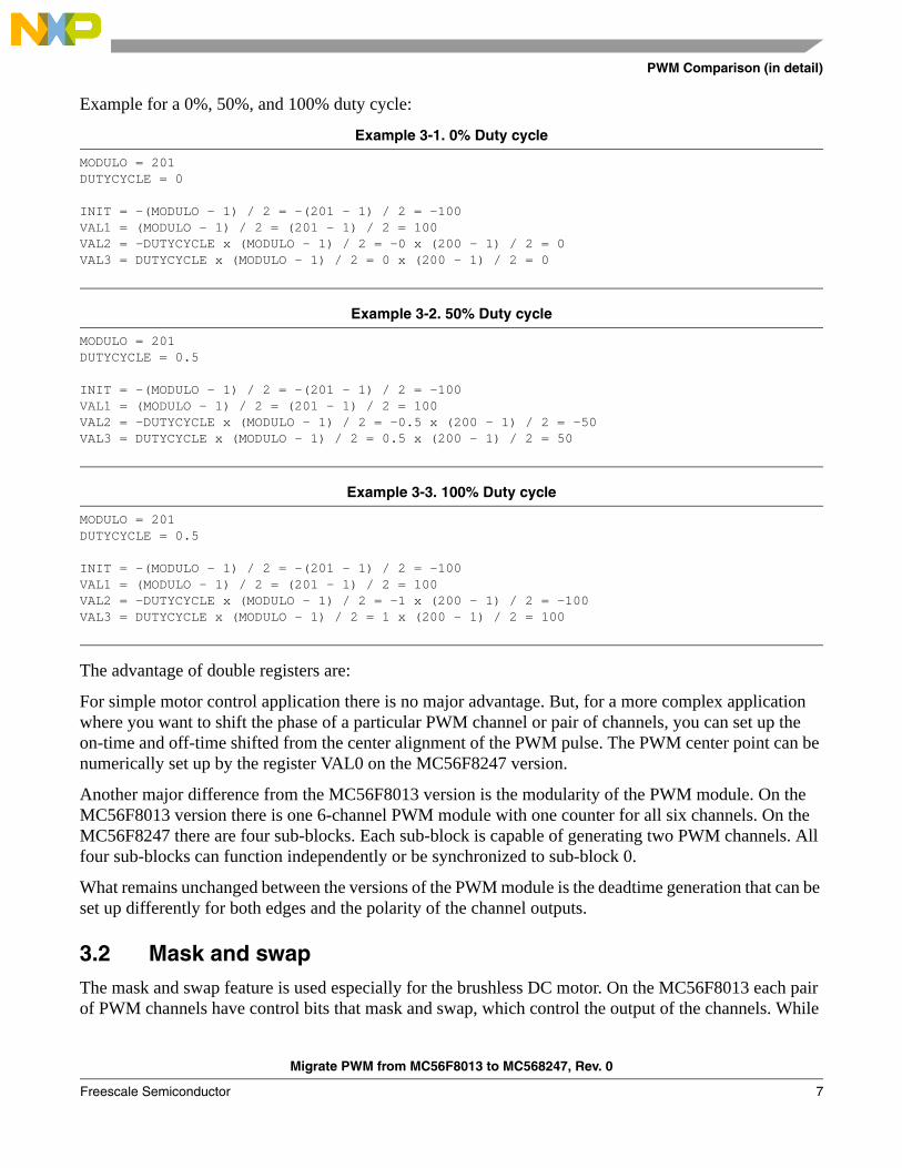
Example for a 0%, 50%, and 100% duty cycle:
Example 3-1. 0% Duty cycle
MODULO = 201DUTYCYCLE = 0
INIT = -(MODULO - 1) / 2 = -(201 - 1) / 2 = -100VAL1 = (MODULO - 1) / 2 = (201 - 1) / 2 = 100VAL2 = -DUTYCYCLE x (MODULO - 1) / 2 = -0 x (200 - 1) / 2 = 0VAL3 = DUTYCYCLE x (MODULO - 1) / 2 = 0 x (200 - 1) / 2 = 0
Example 3-2. 50% Duty cycle
MODULO = 201DUTYCYCLE = 0.5
INIT = -(MODULO - 1) / 2 = -(201 - 1) / 2 = -100VAL1 = (MODULO - 1) / 2 = (201 - 1) / 2 = 100VAL2 = -DUTYCYCLE x (MODULO - 1) / 2 = -0.5 x (200 - 1) / 2 = -50VAL3 = DUTYCYCLE x (MODULO - 1) / 2 = 0.5 x (200 - 1) / 2 = 50
Example 3-3. 100% Duty cycle
MODULO = 201DUTYCYCLE = 0.5
INIT = -(MODULO - 1) / 2 = -(201 - 1) / 2 = -100VAL1 = (MODULO - 1) / 2 = (201 - 1) / 2 = 100VAL2 = -DUTYCYCLE x (MODULO - 1) / 2 = -1 x (200 - 1) / 2 = -100VAL3 = DUTYCYCLE x (MODULO - 1) / 2 = 1 x (200 - 1) / 2 = 100
The advantage of double registers are:
For simple motor control application there is no major advantage. But, for a more complex application where you want to shift the phase of a particular PWM channel or pair of channels, you can set up the on-time and off-time shifted from the center alignment of the PWM pulse. The PWM center point can be numerically set up by the register VAL0 on the MC56F8247 version.
Another major difference from the MC56F8013 version is the modularity of the PWM module. On the MC56F8013 version there is one 6-channel PWM module with one counter for all six channels. On the MC56F8247 there are four sub-blocks. Each sub-block is capable of generating two PWM channels. All four sub-blocks can function independently or be synchronized to sub-block 0.
What remains unchanged between the versions of the PWM module is the deadtime generation that can be set up differently for both edges and the polarity of the channel outputs.
3.2 Mask and swapThe mask and swap feature is used especially for the brushless DC motor. On the MC56F8013 each pair of PWM channels have control bits that mask and swap, which control the output of the channels. While
Migrate PWM from MC56F8013 to MC568247, Rev. 0
Freescale Semiconductor 7
PWM Comparison (in detail)
the mask bit disables the output of the channels, the swap bit swaps the outputs within the pair of channels. These features are controlled by writing software into these bits.
On the MC56F8247, the mask bits and swap bits are also written by the software, but they are applied on the called Force-Out event. This event can be manually written into a register, connected to the reload, or an external signal like timer. In the sensorless BLDC control the timer compare event can make the commutation without any software interaction.
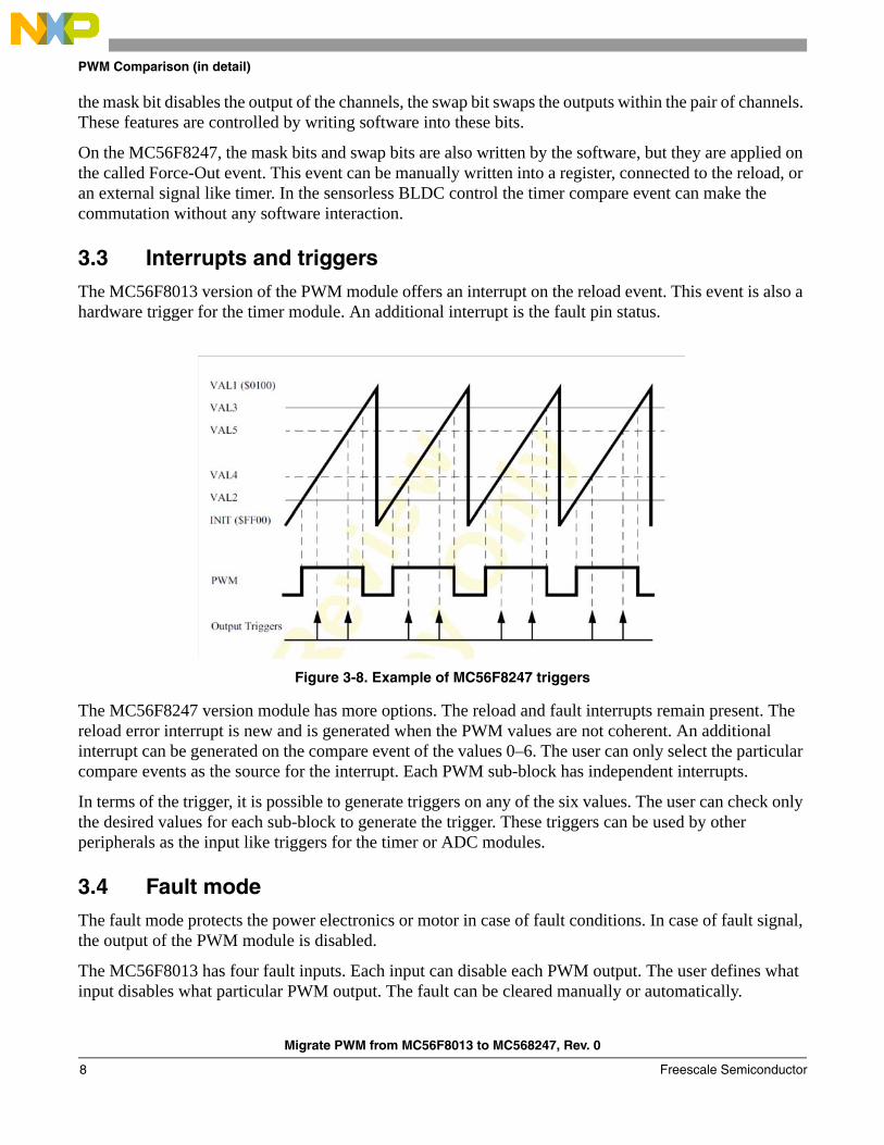
3.3 Interrupts and triggersThe MC56F8013 version of the PWM module offers an interrupt on the reload event. This event is also a hardware trigger for the timer module. An additional interrupt is the fault pin status.
Figure 3-8. Example of MC56F8247 triggers
The MC56F8247 version module has more options. The reload and fault interrupts remain present. The reload error interrupt is new and is generated when the PWM values are not coherent. An additional interrupt can be generated on the compare event of the values 0–6. The user can only select the particular compare events as the source for the interrupt. Each PWM sub-block has independent interrupts.
In terms of the trigger, it is possible to generate triggers on any of the six values. The user can check only the desired values for each sub-block to generate the trigger. These triggers can be used by other peripherals as the input like triggers for the timer or ADC modules.
3.4 Fault modeThe fault mode protects the power electronics or motor in case of fault conditions. In case of fault signal, the output of the PWM module is disabled.
The MC56F8013 has four fault inputs. Each input can disable each PWM output. The user defines what input disables what particular PWM output. The fault can be cleared manually or automatically.
Migrate PWM from MC56F8013 to MC568247, Rev. 0
Freescale Semiconductor8

PWM Set Up Example
On the MC56F8247 the output of each PWM sub-block can be disabled by the four fault inputs. The user has more flexibility to set up what signal goes out from the PWM output in case of fault case. There are three options low, high, or tristated. The fault signal input can be programmed to be active in low or high. The fault clearing can be made manually or automatically. The output is enabled in full or half cycle depending on the user setting.
4 PWM Set Up ExampleAn example on how to set up the PWM module with the following specifications:
• Frequency 20 kHz
• Center-aligned, complementary mode
• Deadtime 800 ns
• Inverted output for the top switches, non-inverted output for the bottom switches
• Fault 0 and 1 sets the outputs to tristated
• 50% duty cycle initialization and output enable
4.1 Module activation
4.1.1 MC56F8013
To enable the clock for the PWM module, you must set up the PWM bit (0) of the register SIM_PCE to 1 .
To enable the PWM module, you must set up the PWMEN bit (0) of the register PWM_CTRL to 1.
It is necessary to correctly set up the GPIO A and B pins to be used as PWM outputs and fault inputs.
4.1.2 MC56F8247
To enable the clock for the PWM module sub-blocks 0, 1, and 3, you must set up the PWMCH0 bit (3), the PWMCH1 bit (2), and the PWMCH2 bit (1) of the register SIM_PCE2 to 1.
It is necessary to set up the GPIO E pins and the Xbar signals to be used as PWM outputs and fault inputs. The GPIOE bit (2) of SIM_PCE0 must be 1 to turn on the GPIO E module. The E5 bit (6) and the E4 bit (4) of SIM_GPS3 must be cleared. These bits select the PWM 2A and 2B as PWM (not XBAR). The bits 0–5 of the GPIOE_PER register must be set to use these pins as PWM (not GPIO).
Example 4-4. Pseudo code
SIM_PCE0 = 0x4 (Enable GPIO E)SIM_PCE2 = 0xE (Enable PWM CH 0, 1, 2)SIM_GPS3 = 0x0 (Select PWM CH 2 A and B outputs)GPIOE_PER = 0x3F (Select PWM CH 0, 1, 2 A & B outputs)
Migrate PWM from MC56F8013 to MC568247, Rev. 0
Freescale Semiconductor 9

PWM Set Up Example
4.2 Frequency
4.2.1 MC56F8013
The clock for the PWM module is 96 MHz (in case of a 3x clock for the PWM, the PCR bit of the SIM_GPS register is set), keeping the prescaler /1, the modulo has to be set up as 96 MHz / 20 kHz = 4800. The center-aligned mode and the counter must count up and down, therefore this number must be divided by 2 to get the correct modulo, that is 2400.
The prescaler is set up by the PRSC bits of the PWM_CTRL register. These bits must be 0.
To set up the modulo, it is necessary to write the value of 2400 to the PWMCM bits of the PWM_CMOD register.
Then the LDOK bit (1) of the PWM_CTRL register must be set for the values to be applied.
4.2.2 MC56F8247
The clock source of the sub-block 0 will be set up to the IPBus clock which means the CLK_SEL bits of the PWM_CTRL2 register will be 0. Sub-block 1 and 2, must be set up to use the clock source of the sub-block 0, these bits will be set to 2.
The prescaler is set up by the PRSC bits of the PWM_CTRL register. These bits must be 0 for each sub-block.
Finally, the LDOK bits (0, 1, 2) of each sub-block must be set to the values to be applied, PWM_MCTRL.
The clock for the PWM module is 60 MHz, keeping the prescaler /1 you must set up the modulo for 3001 (odd to have the symmetry) to achieve 20 kHz, that is the INIT register is –1500 of each sub-block and the VAL1 register is 1500 in the sub-block 0.
To enable the PWM module, set up the RUN bit (8) of the register PWM_MCTRL to 1.
Example 4-5. Pseudo code
PWM_SM0CTRL2 = 0x0 (Input clock for PWM CH 0 is IP Bus clock, complementary)PWM_SM1CTRL2 = 0x2 (Input clock for PWM CH 1 is PWM CH0 clock, complementary)PWM_SM2CTRL2 = 0x2 (Input clock for PWM CH 2 is PWM CH0 clock, complementary)PWM_SM0CTRL = 0x0 (PWM CH 0 prescaler /1)PWM_SM1CTRL = 0x0 (PWM CH 1 prescaler /1)PWM_SM2CTRL = 0x0 (PWM CH 2 prescaler /1)PWM_MCTRL = 0x5 (LDOK bits of PWM CH0, 1, 2)PWM_SM0INIT = -1500 (INIT value; period start)PWM_SM0VAL0 = 0 (VAL0 value; period mid point)PWM_SM0VAL1 = 1500 (VAL1 value; period end)PWM_MCTRL = 0x100 (Run PWM CH0)
Migrate PWM from MC56F8013 to MC568247, Rev. 0
Freescale Semiconductor10

PWM Set Up Example
4.3 Center-aligned, complementary
4.3.1 MC56F8013
To select the center-aligned mode, it is necessary to only set the EDG bit (12) of the PWM_CNFG register to 0.
To select the complementary mode for each pair of PWM outputs it is necessary to set the INDEP01 bit (1), INDEP23 bit (2), and the INDEP45 bit (3) to the value of 0.
4.3.2 MC56F8247
To select the complementary mode for each pair of PWM outputs, it is necessary to clear the INDEP bit (13) of the PWM_CTRL2 register of the sub-block 0, 1, and 2 to the value of 0.
There is no special bit to select the center-aligned or edge-aligned PWM output. To reach the center aligned PWM, the VAL2 and VAL3 values must be supplied symmetrically between the INIT and VAL1 value. Thus, to get 50% duty cycle center-aligned, it is necessary to supply VAL2 with –750 and VAL3 with 750 (because the INIT is –1500 and VAL1 is 1500).
Finally, the LDOK bits (0, 1, 2) of each sub-block must be set for the values applied.
Example 4-6. Pseudo code
PWM_SM0CTRL2 &= ~0x2000 (complementary)PWM_SM1CTRL2 &= ~0x2000 (complementary)PWM_SM2CTRL2 &= ~0x2000 (complementary)PWM_SM0VAL2 = -750 (PWM CH0 50% duty cycle)PWM_SM0VAL3 = 750 (PWM CH0 50% duty cycle)PWM_SM1VAL2 = -750 (PWM CH1 50% duty cycle)PWM_SM1VAL3 = 750 (PWM CH1 50% duty cycle)PWM_SM2VAL2 = -750 (PWM CH2 50% duty cycle)PWM_SM2VAL3 = 750 (PWM CH2 50% duty cycle)PWM_MCTRL = 0x5 (LDOK bits of PWM CH0, 1, 2)
4.4 Deadtime
4.4.1 MC56F8013
The deadtime is derived from the PWM module clock. To set up the deadtime of 800 ns, it is necessary to fill the PWMDT0 bits of the register PWM_DT IM0 and the PWMDT1 bits of the register PWM_DTIM1 with the value of 26.
4.4.2 MC56F8247
The deadtime is derived from the PWM module clock. To set up the deadtime of 800 ns it is necessary to fill the DTCNT0 bits of the register DTCNT0 and the DTCNT1 bits of the DTCNT1 register with the values of 48. These registers must be updated in all the used sub-blocks.
Migrate PWM from MC56F8013 to MC568247, Rev. 0
Freescale Semiconductor 11

PWM Set Up Example
Example 4-7. Pseudo code
PWM_SM0DTCNT0 = 48 (PWM CH0 A deadtime)PWM_SM0DTCNT1 = 48 (PWM CH0 B deadtime)PWM_SM1DTCNT0 = 48 (PWM CH1 A deadtime)PWM_SM1DTCNT1 = 48 (PWM CH1 B deadtime)PWM_SM2DTCNT0 = 48 (PWM CH2 A deadtime)PWM_SM2DTCNT1 = 48 (PWM CH2 B deadtime)
4.5 Faults
4.5.1 MC56F8013
To configure only Fault 0 and Fault 1 signals to disable all the PWM channels, it is necessary to program the register PWM_DMAP0 with the value 0x3333, and the PWMDMA1 register with the value 0x33.
It is then necessary to set up generation on the fault event. This is done by filling the bits FIE0 (1) and FIE1(3) with 0 to turn off the interrupt or 1 to turn on the interrupt. These bits are in the PWM_FCTRL register. To select the manual fault clearing, it is necessary to clear the bits FMODE0 (0) and FMODE1 (0) of the same register. In case of the automatic fault clearing these bits must be set.
4.5.2 MC56F8247
To configure only Fault 0 and Fault 1 signals to disable all the used PWM channels, the PWM_DISMAP register of the sub-block 0, 1 and 2 must be filled with the values 0xF033.
To set up the tristated output of the channels in case of the fault signal, it is necessary to fill the PWM_PWMAFS and PWM_PWMBFS bits of the sub-block 0, 1 and 2 PWM_OCTRL register to the value of 2.
Any possible fault flags (FFLAG) are to be cleared in the PWM_FSTS register by writing 1 to all faults flags, that is 0x0F.
Example 4-8. Pseudo code
PWM_SM0DISMAP = 0xF033 (PWM CH0 A & B disabled fault by PWM fault 0 & 1)PWM_SM1DISMAP = 0xF033 (PWM CH1 A & B disabled fault by PWM fault 0 & 1)PWM_SM2DISMAP = 0xF033 (PWM CH2 A & B disabled fault by PWM fault 0 & 1)PWM_SM0OCTRL = 0x28 (tristated on PWM CH0 A & B when fault)PWM_SM1OCTRL = 0x28 (tristated on PWM CH0 A & B when fault)PWM_SM2OCTRL = 0x28 (tristated on PWM CH0 A & B when fault)PWM_SM0STS = 0xF (clear PWM CH0 fault flags)PWM_SM1STS = 0xF (clear PWM CH1 fault flags)PWM_SM2STS = 0xF (clear PWM CH2 fault flags)
Migrate PWM from MC56F8013 to MC568247, Rev. 0
Freescale Semiconductor12

PWM Set Up Example
4.6 5o% Duty cycle initialization and output enable
4.6.1 MC56F8013
To set the duty cycles to 50% it is necessary to fill the PWM_VAL0, PWM_VAL2 and PWM_VAL4 registers with the value that is half of the modulo, that is 800 / 2 = 400. Then the LDOK bit (1) and the PWM_CTRL register must be set for the values to be applied.
To enable the PWM output on the pins, it is necessary to write one into the PAD_EN bit (15) of the PWM_OUT register.
4.6.2 MC56F8247
To set the duty cycles to 50% it is necessary to set correctly the PWM_VAL2 and PWM_VAL3 registers of the sub-block 0, 1, and 2. As the counter counts from –1500 to 1500, to get the 50% duty cycle the PWM_VAL2 register must be set to –750 and the PWM_VAL3 register, to 750. Finally, the LDOK bits (0, 1, 2) of each sub-block must be set for the values to be applied.
To enable the PWM output on the pins, it is necessary to write 0x7 to the PWMA_EN (8, 9, 10) and PWMB_EN (4, 5, 6) bits of the PWM_OUTEN register.
Example 4-9. Pseudo code
PWM_SM0VAL2 = -750 (PWM CH0 50% duty cycle)PWM_SM0VAL3 = 750 (PWM CH0 50% duty cycle)PWM_SM1VAL2 = -750 (PWM CH1 50% duty cycle)PWM_SM1VAL3 = 750 (PWM CH1 50% duty cycle)PWM_SM2VAL2 = -750 (PWM CH2 50% duty cycle)PWM_SM2VAL3 = 750 (PWM CH2 50% duty cycle)PWM_MCTRL = 0x5 (LDOK bits of PWM CH0, 1, 2)PWM_OUTEN = 0x0770 (PWM output enable)
4.7 BLDC commutationThis is an example where outputs running are needed:
• Phase A non-swapped
• Phase B with no output
• Phase C swapped.
The static setting of the module remains the same from the previous chapters.
4.7.1 MC56F8013
To keep the output of the channels 0 and 1 non-swapped, the bit SWP01 (0) of the PWM_CCTRL register must be cleared. Channel 4 and 5 are swapped, therefore the bit SWP45 (2) must be set. Channel 0, 1, 4, 5 must now be unmasked, so the bits MSK0 (8), MSK1 (9), MSK4 (12), MSK5 (13), or the PWM_CCTRL register must be cleared. To mask the channels 2 and 3, the bits MSK2 (10) and MSK3 (11) must be set.
Migrate PWM from MC56F8013 to MC568247, Rev. 0
Freescale Semiconductor 13

Conclusion
4.7.2 MC56F8247
First, the FORCE_OUT feature must be properly set. The bit FRCEN (7) in the sub-block 0’s PWM_CTRL2 register must be set. When the force signal arrives, the counter is initialized. The condition is to have this bit set on. The FORCE_SEL bits of the sub-block 1 and sub-block 2 must be set to 1 to be forced by the force signal of the sub-block 0. Setting for the sub-block 0 depends if the user wants to force the change manually, and it can be set to 0. If it is forced by an external signal (timer), set it to 6.
To keep the output of the channels of the sub-block 0 non-swapped, the bits SM0SEL23 of the PWM_DTSRCSEL register must be cleared. Swap the sub-block 2’s channels, therefore the bits SM2SEL23 must be filled with the value of 1. The channels of the sub-block 0 and 3 must now be unmasked, the bits MASKA and MASKB of sub-block 0 and sub-block 2 will be cleared in the PWM_MASK register (bits 4, 6, 8, 10). To mask the sub-block 1’s channels, the bits MASKA and MASKB of the sub-block1 must be set (bits 5, 9).
Finally, the FORCE_OUT signal must be generated. If the user selected the manual option of the force signal, then the FORCE bit of the PWM_CTRL2 register of the sub-block 0 must be set. This causes the force event. If it was set as the external signal from the timer, the force event will occur when the timer compare event generates the signal.
Example 4-10. Pseudo code with manual trigger
PWM_SM0CTRL2 |= 0x80 (To enable force out event with manual trigger)PWM_SM1CTRL2 |= 0x40 (To be forced by the sub-module 0)PWM_SM2CTRL2 |= 0x40 (To be forced by the sub-module 0)PWM_DTSRCSEL = 0x0400 (To be swapped the outputs of the sub-block 2)PWM_MASK = 0x0220 (To mask the sub-block 1’s outputs)PWM_SM0CTRL2 |= 0X0040 (To generate the force event)
5 ConclusionThe MC56F8247 PWM module is a complex and flexible peripheral in the market. Therefore, it was not possible to describe all possible settings. The user should consult the manual of this peripheral to understand how powerful this peripheral is.
Migrate PWM from MC56F8013 to MC568247, Rev. 0
Freescale Semiconductor14

Migrate PWM from MC56F8013 to MC568247, Rev. 0
Freescale Semiconductor 15
THIS PAGE IS INTENTIONALLY BLANK
Document Number: AN4319Rev. 006/2011
How to Reach Us:
Home Page:www.freescale.com
Web Support:http://www.freescale.com/support
USA/Europe or Locations Not Listed:Freescale Semiconductor, Inc.Technical Information Center, EL5162100 East Elliot RoadTempe, Arizona 85284+1-800-521-6274 or +1-480-768-2130www.freescale.com/support
Europe, Middle East, and Africa:Freescale Halbleiter Deutschland GmbHTechnical Information CenterSchatzbogen 781829 Muenchen, Germany+44 1296 380 456 (English)+46 8 52200080 (English)+49 89 92103 559 (German)+33 1 69 35 48 48 (French)www.freescale.com/support
Japan:Freescale Semiconductor Japan Ltd.HeadquartersARCO Tower 15F1-8-1, Shimo-Meguro, Meguro-ku,Tokyo 153-0064Japan0120 191014 or +81 3 5437 [email protected]
Asia/Pacific:Freescale Semiconductor China Ltd.Exchange Building 23FNo. 118 Jianguo RoadChaoyang DistrictBeijing 100022 China +86 10 5879 [email protected]
For Literature Requests Only:Freescale Semiconductor Literature Distribution Center1-800-441-2447 or 303-675-2140Fax: [email protected]
Information in this document is provided solely to enable system and software implementers to use Freescale Semiconductor products. There are no express or implied copyright licenses granted hereunder to design or fabricate any integrated circuits or integrated circuits based on the information in this document.
Freescale Semiconductor reserves the right to make changes without further notice to any products herein. Freescale Semiconductor makes no warranty, representation or guarantee regarding the suitability of its products for any particular purpose, nor does Freescale Semiconductor assume any liability arising out of the application or use of any product or circuit, and specifically disclaims any and all liability, including without limitation consequential or incidental damages. “Typical” parameters that may be provided in Freescale Semiconductor data sheets and/or specifications can and do vary in different applications and actual performance may vary over time. All operating parameters, including “Typicals”, must be validated for each customer application by customer’s technical experts. Freescale Semiconductor does not convey any license under its patent rights nor the rights of others. Freescale Semiconductor products are not designed, intended, or authorized for use as components in systems intended for surgical implant into the body, or other applications intended to support or sustain life, or for any other application in which the failure of the Freescale Semiconductor product could create a situation where personal injury or death may occur. Should Buyer purchase or use Freescale Semiconductor products for any such unintended or unauthorized application, Buyer shall indemnify and hold Freescale Semiconductor and its officers, employees, subsidiaries, affiliates, and distributors harmless against all claims, costs, damages, and expenses, and reasonable attorney fees arising out of, directly or indirectly, any claim of personal injury or death associated with such unintended or unauthorized use, even if such claim alleges that Freescale Semiconductor was negligent regarding the design or manufacture of the part.
RoHS-compliant and/or Pb-free versions of Freescale products have the functionality and electrical characteristics as their non-RoHS-compliant and/or non-Pb-free counterparts. For further information, see http://www.freescale.com or contact your Freescale sales representative.
For information on Freescale’s Environmental Products program, go to http://www.freescale.com/epp.
Freescale™ and the Freescale logo are trademarks of Freescale Semiconductor, Inc. All other product or service names are the property of their respective owners.© Freescale Semiconductor, Inc. 2011. All rights reserved.