Microsystem Technologies for Biomedical Applications
26
0 Microsystem Technologies for Biomedical Applications Francisco Perdigones, Jos´ e Miguel Moreno, Antonio Luque, Carmen Aracil and Jos´ e Manuel Quero University of Seville Spain 1. Introduction Microsystems, also often known as microelectromechanical systems (MEMS), are miniaturized devices fabricated using techniques called “micromachining”, and that are common in different application areas, such as automotive, consumer electronics, industrial measurements, and recently biomedical too Dean & Luque (2009). The typical definition states that a microsystem is any device which has at least one feature size in the order of micrometers (1:1000 of a mm). Historically, silicon has been used as the material of choice for fabricating microsystems, due to the processing equipment which was already available in microelectronics foundries, and the thorough understanding of the properties that the impressive development of electronics in the 1950s and 60s made possible. Another advantage derived from microelectronics is the low cost associated when fabricating devices at very large production volume. It was then natural to try to integrate other devices with the microelectronic chips, and so the first microsystems were born. Initially, the market was driven by automotive applications, and accelerometers for stability control and airbag deployment were one of the first commercial successes of microsystems technology. Other typical examples from this age are pressure sensors and inkjet printer nozzles. Since then, the global MEMS market has not ceased to grow, and their applications are more diverse now. It is expected that by 2010 more than 8000 million MEMS devices will be sold yearly Status of the MEMS industry (2008). As explained before, due to the importance of the microelectronics foundries, silicon is nowadays a widely available material, with a relatively low cost. Its mechanical and electrical properties have been very well known for decades, a fact which still makes it an ideal choice for many microsystems. Silicon is nearly as strong as steel, but with a much lower fracture toughness Petersen (1982). It is usually sold in circular wafers of varying diameters, from 100 to 500 mm. In microsystems, the final devices are sometimes built by removing part of the material in the substrate, in a process called bulk micromachining, while in other occasions, thin films are deposited on top of the wafer and then parts of them are etched away to form the device, which is known as surface micromachining Kovacs et al. (1998). The actual micromachining of silicon is performed using etchants, which can be liquid (wet etching) or in gas or plasma form (dry etching). Both types can etch the silicon isotropically or anisotropically, depending on the etchant composition and operating parameters. Other materials are commonly present in silicon-based microsystems, most of which also derive from silicon, such as polycrystalline silicon, silicon dioxide, or silicon nitride. Thin or thick 3 www.intechopen.com
Transcript of Microsystem Technologies for Biomedical Applications

0
Microsystem Technologies for BiomedicalApplications
Francisco Perdigones, Jose Miguel Moreno,Antonio Luque, Carmen Aracil and Jose Manuel Quero
University of SevilleSpain
1. Introduction
Microsystems, also often known as microelectromechanical systems (MEMS), areminiaturized devices fabricated using techniques called “micromachining”, and thatare common in different application areas, such as automotive, consumer electronics,industrial measurements, and recently biomedical too Dean & Luque (2009). The typicaldefinition states that a microsystem is any device which has at least one feature size in theorder of micrometers (1:1000 of a mm).Historically, silicon has been used as the material of choice for fabricating microsystems, dueto the processing equipment which was already available in microelectronics foundries, andthe thorough understanding of the properties that the impressive development of electronicsin the 1950s and 60s made possible. Another advantage derived from microelectronics isthe low cost associated when fabricating devices at very large production volume. It wasthen natural to try to integrate other devices with the microelectronic chips, and so the firstmicrosystems were born. Initially, the market was driven by automotive applications, andaccelerometers for stability control and airbag deployment were one of the first commercialsuccesses of microsystems technology. Other typical examples from this age are pressuresensors and inkjet printer nozzles. Since then, the global MEMS market has not ceased togrow, and their applications are more diverse now. It is expected that by 2010 more than 8000million MEMS devices will be sold yearly Status of the MEMS industry (2008).As explained before, due to the importance of the microelectronics foundries, silicon isnowadays a widely available material, with a relatively low cost. Its mechanical and electricalproperties have been very well known for decades, a fact which still makes it an ideal choicefor many microsystems. Silicon is nearly as strong as steel, but with a much lower fracturetoughness Petersen (1982). It is usually sold in circular wafers of varying diameters, from100 to 500 mm. In microsystems, the final devices are sometimes built by removing partof the material in the substrate, in a process called bulk micromachining, while in otheroccasions, thin films are deposited on top of the wafer and then parts of them are etchedaway to form the device, which is known as surface micromachining Kovacs et al. (1998).The actual micromachining of silicon is performed using etchants, which can be liquid (wetetching) or in gas or plasma form (dry etching). Both types can etch the silicon isotropicallyor anisotropically, depending on the etchant composition and operating parameters. Othermaterials are commonly present in silicon-based microsystems, most of which also derivefrom silicon, such as polycrystalline silicon, silicon dioxide, or silicon nitride. Thin or thick
3
www.intechopen.com

2 Biomedical Engineering, Trends, Researches and Technologies
films of other materials can be deposited on top of the substrate using chemical vapordeposition (CVD), sputtering, thermal evaporation, or spin coating, among other techniques.All the mentioned process are complemented by photolithography, by means of which aparticular area of the wafer where to etch or deposit a material can be selected. This is doneusing a photosensitive resist which is exposed to light (usually ultraviolet) through a maskwith opaque and transparent areas. The resist is then developed and the exposed areas areremoved (if the photoresist is positive). The remaining photoresist protects the wafer andavoid that area to be etched away, or a material to be deposited on top of it.Silicon has been used successfully to fabricate devices such as microfluidic control valves,blood micropumps and microneedles for drug delivery through the skin Henry et al. (1998),but other materials are of more importance for biomedical applications. These materials areusually polymers, which offer the advantage of being cheap and fast to process, especially forsmall-scale production. Many of the polymers used are biocompatible.Two of the most common used polymers are PMMA (poly-methyl-metacrylate) and PDMS(poly-dimethyl-siloxane). PMMA is available in solid form, and thermal casting or moldingare used to shape it Huang & Fu (2007). PDMS is available as two liquid products (prepolymerand curing agent), which should be mixed together, poured over a mold, and cured atmoderately high temperatures. Then it becomes solid and can be demolded. This processhas been widely adopted by the microfluidics and biomedical communities since it wasdeveloped in 2000 Duffy et al. (1998). Another material used in rapid prototyping is thenegative photoresist called SU-8. Examples of actual devices built using PDMS and SU-8will be showcased below.The measurement of substances in the blood was one of the first biomedical applications ofMEMS devices. Nowadays, personal glucometers are inexpensive, and some of them arestarting to include an insulin pump, also built with MEMS technology, which is able to deliverinsulin to the patient when the measured glucose level is too high.One of the most important goals of the research in BioMEMS is the fabrication of a lab-on-chip(LOC) device, where all the needed components to perform extraction, movement, control,processing, analysis, etc. of biological fluids are present. This LOC device would be a trulyminiaturized laboratory, which would fulfill many of today’s needs in portable medicine.To accomplish a task like building a LOC, many smaller parts must be considered. In the restof the sections of this chapter, these parts will be discussed. Section 2 will discuss in detailthe fabrication processes for the materials described above, which are the most commonlyused now. In Section 3, the issue of power supply will be considered, and some solutions tointegrate the microfluidic power in the microsystemwill be presented. Section 4will deal withcontrol and regulation of biological fluids inside the chip. In Section 5, the integration of thedifferent components will be discussed, giving some examples of actual devices, and finallyin Section 6, some conclusions will be remarked.
2. Fabrication processes for biocompatible materials
2.1 IntroductionIn this section the basis of fabrication processes using the most commonlybiocompatible polymers used in MEMS are reported. These materials areGlycidyl-ether-bisphenol-A novolac (SU-8) Lorenz et al. (1997) and polydimethilsiloxane(PDMS) McDonald & Whitesides (2002).Regarding SU-8 fabrication processes, the typical fabrication process and multilayer techniqueMata et al. (2006) are presented in this introduction. Then, in section 2.3 a new process to
46 Biomedical Engineering Trends in Electronics, Communications and Software
www.intechopen.com
Microsystem Technologies for Biomedical Applications 3
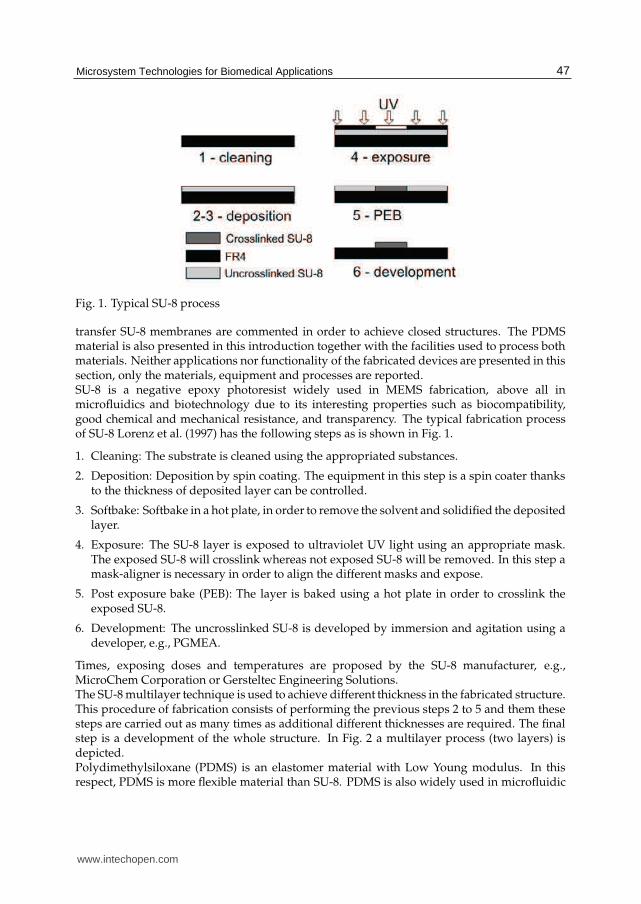
Fig. 1. Typical SU-8 process
transfer SU-8 membranes are commented in order to achieve closed structures. The PDMSmaterial is also presented in this introduction together with the facilities used to process bothmaterials. Neither applications nor functionality of the fabricated devices are presented in thissection, only the materials, equipment and processes are reported.SU-8 is a negative epoxy photoresist widely used in MEMS fabrication, above all inmicrofluidics and biotechnology due to its interesting properties such as biocompatibility,good chemical and mechanical resistance, and transparency. The typical fabrication processof SU-8 Lorenz et al. (1997) has the following steps as is shown in Fig. 1.
1. Cleaning: The substrate is cleaned using the appropriated substances.
2. Deposition: Deposition by spin coating. The equipment in this step is a spin coater thanksto the thickness of deposited layer can be controlled.
3. Softbake: Softbake in a hot plate, in order to remove the solvent and solidified the depositedlayer.
4. Exposure: The SU-8 layer is exposed to ultraviolet UV light using an appropriate mask.The exposed SU-8 will crosslink whereas not exposed SU-8 will be removed. In this step amask-aligner is necessary in order to align the different masks and expose.
5. Post exposure bake (PEB): The layer is baked using a hot plate in order to crosslink theexposed SU-8.
6. Development: The uncrosslinked SU-8 is developed by immersion and agitation using adeveloper, e.g., PGMEA.
Times, exposing doses and temperatures are proposed by the SU-8 manufacturer, e.g.,MicroChem Corporation or Gersteltec Engineering Solutions.The SU-8multilayer technique is used to achieve different thickness in the fabricated structure.This procedure of fabrication consists of performing the previous steps 2 to 5 and them thesesteps are carried out as many times as additional different thicknesses are required. The finalstep is a development of the whole structure. In Fig. 2 a multilayer process (two layers) isdepicted.Polydimethylsiloxane (PDMS) is an elastomer material with Low Young modulus. In thisrespect, PDMS is more flexible material than SU-8. PDMS is also widely used in microfluidic
47Microsystem Technologies for Biomedical Applications
www.intechopen.com

4 Biomedical Engineering, Trends, Researches and Technologies
Fig. 2. Multilayer SU-8 process
circuits and biotechnology as base material. It is composed by a prepolymer and a curingagent that must be mixed in order to obtain the PDMS. Depending on the ratio of bothsubstances the PDMS will require a certain time of curing for a fixed temperature. Theequipment necessary to process PDMS includes a vacuum chamber to remove the bubblesthat appear during mixing and an oven to cure the PDMS. The fabrication of PDMS device ispreceded by molds fabrication. These molds are necessary to define the PDMS structure as itwill be explained.
2.2 PDMS fabrication processesThe fabrication using PDMS elastomer is based on soft lithography McDonald & Whitesides(2002). The procedure starts with the fabrication of molds. There are several techniques tofabricate these molds, among others, photolithography or micromachining. The substratewidely used for photolithography is silicon, and the material to define the structuresis SU-8. The molds are fabricated using the typical process of SU-8 or using morecomplex techniques as multilayer fabrication. The low adherence of PDMS to SU8 andsilicon facilitates the demolding process. We propose Flame Retadant 4 (FR4) of PrintedCircuit Board (PCB) as substrate due to its low cost and good adherence with SU-8,Perdigones, Moreno, Luque & Quero (2010). However this material presents more roughnessthan silicon or pyrex but no problems have been observed due to this issue. Amold fabricatedperforming the typical process with FR4 as substrate and SU-8 can be seen as an example inFig. 3. As it is explained later, the PDMSwill be poured over it, achieving the negative patternof the mold.Once the molds have been produced, a mixture of prepolymer and curing agent is performedwith a commonly used ratio in weight percent of 10:1. This mixture is performed by agitationusing a stirring bar, and then is degassed in order to remove the bubbles that appear duringmixing. Once the mixture has been degassed, it is poured over the mold and put into anoven at 65 ◦C during 1 h approximately until PDMS is crosslinked and solidified. Finally, thePDMS is peeled off the mold. Using this method only opened structures or microchannels canbe fabricated.There are several techniques of PDMS to PDMS bonding in order to complete the fabricationand achieve the closed structures Eddings et al. (2008). Among these techniques, Partial
48 Biomedical Engineering Trends in Electronics, Communications and Software
www.intechopen.com

Microsystem Technologies for Biomedical Applications 5
Fig. 3. Fabricated mold using FR4 as substrate and SU-8 to define the structure. The SU-8patterned layer defines a microchannel with an internal column due to the central cavity.
Curing, Uncured PDMS adhesive and Varing Curing Ratio are the most interesting ones dueto their high average bond strengths. In literature, authors propose different temperatures,baking times and ratios to perform the bonding using these techniques. In this respect, ourgroup uses a combination of Partial Curing and Varing Curing Ratio with successful resultsin multilayer fabrication. We use a ratio 20:1 and 10:1 alternatively, i.e., 20:1 for the first layer,10:1 for the second one, for the third layer 20:1, etc. The baking times can be selected in arange of 30-45 min for 10:1 ratio, and 50-60 min for 20:1 ratio, at 65 ◦C in an oven. Finally, thebonding is performed at 65 ◦C during 2 h in the oven. In Fig. 4, the PDMS part of an extractorof liquid for submicroliter range Perdigones, Luque & Quero (2010b) can be seen.In order to fabricate the PDMS structure shown in Fig. 4 only one mold is necessary. Theprocedure of fabrication is very simple, where two PDMS pieces are bonded. This process canbe seen in Fig. 5 and it starts with the fabrication of the mold using the SU-8 typical procedure.Once the mold has been done, a PDMS with a ratio of 10:1 is poured over it (layer 1), step (a),
Fig. 4. PDMS extractor of liquid for submicroliter range.
49Microsystem Technologies for Biomedical Applications
www.intechopen.com

6 Biomedical Engineering, Trends, Researches and Technologies
Fig. 5. Fabrication process for the structure in Fig. 4
and other mixture of 20:1 is spin coated over a glass substrate (layer 2), step (b). The layersare put into an oven at 65 ◦C during 45 min for the first one and 1 h for the second one. Then,the layer 1 is demolded and put into contact to layer 2, (step c), as can be seen in Fig. 5 and thebonding is performed in an oven at 65 ◦C during 2 h. Once the bonding has been performed,the final structure is peeled off the glass substrate and the layer 2 is punched out.A more complex PDMS three dimensional structure with three different layers and fabricatedusing the presented process is shown in Fig. 6. This is a cross section of a PDMS flow regulatorwith positive gain as will commented in section 4.The process to fabricate the structure in Fig. 6 requires two molds and is shown in Fig. 7. Thefirst one (mold 1) is made using the typical process and the second one (mold 2) using themultilayer technique. The procedure starts performing three mixtures with a ratio 10:1 forthe intermediate layer (layer 2) and 20:1 for the rest. Once the mixtures have been degassed,the mixture 10:1 is spin coated over the mold 1 in order to achieve a structure (layer 2) witha membrane on top (step a). Next, one of 20:1 mixture is poured over the mold 2 (step b)defining the layer 1, and the other is spin coated over a glass substrate (step c) defining thelayer 3. All layers are put into an oven at 65 ◦C during 30 min for layer 2 and 1 h for therest. Once the PDMS layers are partially curing, layer 1 is demolded and put into contact withlayer 2 as can be seen in step d. Both layers are put into an oven at 65 ◦C during 5 min in orderto achieve a initial bonding. This bonding is necessary to demold layer 2 without breaks thatmight appear due to its low thickness. Once this initial bonding is performed, the structure is
Fig. 6. Three dimensional PDMS structure with three layers
50 Biomedical Engineering Trends in Electronics, Communications and Software
www.intechopen.com

Microsystem Technologies for Biomedical Applications 7
Fig. 7. Fabrication process for the structure in Fig. 6
demolded frommold 1, and put into contact with layer 3 as can be seen in step e. Next, thesethree layers are bonding at room temperature during 24 h because the air in the cavities couldexpand and lead the separation between layer 2 and 3. After this step, the final structure is putin a hot plate at 50 ◦C during 5 min to ensure a good bonding and then the device is peeledoff the glass substrate.
2.3 SU-8 closed structuresA special effort is associated to processes which achieve 3D structures to fabricatemicrochannels and microreservoirs, taking into account that SU-8 typical process is focusedfor the fabrication of open structures.Different ways to achieve SU-8 closed structures have been reported but mainly we can findtwo trends. The first approach employs sacrificial layers, where uncrosslinked SU-8 is usedas base to obtain upper layers and afterwards it is removed. A microchannel fabricatedby this method is shown in Fig.8. The significant disadvantages of this approach are thelimitation of the design of structures with an aperture to strip off the uncrosslinked SU-8, andan excessive development time for the required multilayer deposition Chung & Allen (2005).However, in recent years there is an evolution in various aspects of this approach improvingthe mask-process Guerin et al. (1997), embedding the masks Haefliger & Boisen (2006), andcontrolling the exposure, Chuang et al. (2003).The second trend widely used, consists in sealing the SU-8 structure by means of transferringSU-8 layers. In this way, the use of removable films to transfer SU-8 layers obtainingmonolithic devices by lamination has been broadly reported. Many different materials areused as removable layer, among others, PDMS Patel et al. (2008), PET Abgrall et al. (2008),kapton Ezkerra et al. (2007). Besides from using different materials, there are plenty of flowprocesses based in the transfer of the SU-8 layers as well. An important requirement in thedevelopment of processes is the compatibility with previous processes to be able to improvethe complexity and integration with other devices.
51Microsystem Technologies for Biomedical Applications
www.intechopen.com

8 Biomedical Engineering, Trends, Researches and Technologies
Fig. 8. Flow of fabrication process of a sacrificial layer process.
A particular example of this approach is the transferring process has been namedBETTS Aracil, Perdigones, Moreno & Quero (2010) (Bonding, UV Exposing and TransferringTechnique in SU-8). The key step of this process is the use of the layer substrate not only totransfer the SU-8 layer, but also to act as a mask to pattern the SU-8 layer and to allow peelingoff the transferred film easily. Therefore, bonding, UV exposing and transferring processesare carried out in a single step. The process flow of BETTS can be seen in Fig. 9. The transferprocess can be achieved over different kind of substrates, like glass, silicon, SU-8 or FR4, whatextends the number of applications that can use of it. The thickness of the transferred layeris variable according to the application. Its value is very closed linked to the height of themicrochannel. The shallowest microchannel fabricated corresponds to 40µm, for a thicknessof the transferred layer of 5µm. The compatibility with others fabrication processes allowsthe integration with other electronic devices wire bonded to the substrate. 3D structures areeasily manufactured by means of the repetition of the flow of process. An example of 3Dmultichannel network is shown in Fig. 10.
3. Autonomous microdevices
3.1 Pressure chambersNowadays, an important challenge still to be overcome in the field of Lab on Chip devicesis the improvement of portability and fluid flow generation. Although there is a widerange of methods to develop fluid flow in microfluidic devices such as electroosmoticflow, electrokinetic pumps or by centrifugal force or capillary action, Laser & Santiago(2004); Lim et al. (2010), on-chip pumping is in general externally generated by traditionalmacroscale syringe or vacuum pumps. This limitation makes LOC devices encapsulationand portability a very difficult task when developing miniaturized autonomous microfluidicsystems. Moreover, MEMS packaging results more expensive compared to the microsystemitself when considering vacuum or pressure sealing, being indispensable to find simple andlow cost encapsulationmethods fully compatible and easy to integrate with former fabricationprocesses and materials.
52 Biomedical Engineering Trends in Electronics, Communications and Software
www.intechopen.com

Microsystem Technologies for Biomedical Applications 9
Fig. 9. Flow of fabrication process of a transferring process named BETTS.
Peristaltic micropumps have been widely used for LOC fluid flow generation, allowing thetransport of a controlled fluid volume in clinical diagnosis and drug delivery applicationsKoch et al. (2009). Nevertheless, this alternative presents some disadvantages such as thelarge area required in the LOC device and the high power consumption to impulse the fluid.The solution presented in this chapter to minimize these limitations is the use of disposablemicrofluidic devices, based on a single use thermo-mechanical microvalve activation whichreleases a stored pressure to achieve a controlled fluid flow impulsion. This system can beeasily integrated in a small area of the LOC, providing a portable reservoir of pneumaticenergy.The mechanism of differential pressure is a well known method in microfluidic fluid flowimpulsion, where the use of epoxy resins such as SU-8 opens up new possibilities for theimplementation of pressure-driven flow on-chip. Although polymers are typically severalorders of magnitude more permeable to gas leakages than glass or metals, epoxy resins arecharacterized by a low gas permeability and thus can be used for simple and low-cost sealingof packages Murillo et al. (2010). In addition to this, SU-8 epoxy shows a decrease in gaspermeability when the level of crosslinking is increased, being a suitable and interestingalternative for pressurized or vacuum microchambers fabrication Metz et al. (2004).
53Microsystem Technologies for Biomedical Applications
www.intechopen.com

10 Biomedical Engineering, Trends, Researches and Technologies
In this section two portable pressure driven flow devices for LOC applications are presented:vacuum and pressurized chambers.The pressurized system consists in a monolithical SU-8 structure composed by a sealedmicrochamber connected to a valve that will be introduced in section 3.2. The chamberstructure is connected to a microfluidic channel to seal it at a fixed and controlled pressureby an extra UV isolation step compatible with the traditional SU-8 fabrication process. Thepressurized portable system SU-8 layout is shown in Fig. 11. To seal the chamber and store afluid at a fixed pressure, low-viscous SU-8 is externally injected in the chamber hole throughthe control serpentine microchannel by means of a compressed air supply connected to apressure transducer. The viscosity of the SU-8 supplied by Microchem is determined by themanufacturer by means of a code number (2005, 2025, 2150, etc.), where the lower numbermeans lower SU-8 viscosity. Thus, to seal the chamber SU-8 2005 is employed. The dimensionsof the microchannel are previously calculated according to the isothermal process for an idealgas and the Boyle’s law:
PV = k→ P1V1 = P2V2, (1)
Where P1 is the desired final pressure in the microchamber, V1 is its volume, P2 is the initialpressure before sealing process (atmospheric pressure), V2 the total air volume inside thestructure and k is a constant. When the SU-8 2005 is injected through the inlet, the air volumeentrapped inside the control channel at atmospheric pressure pushes the air in the chamber,proportionally increasing its pressure depending on the expression (1). As an example, thecontrol microchannel area in the layout is calculated to be the same than the chamber area,in order to obtain 2 bar absolute pressure inside the chamber. Then, an UV exposure steppolymerizes the liquid SU-8 inside the control channel to seal hermetically the chamber whichis pressurized and ready for use. The stored pneumatic energy of the gas inside the chamberis expressed as follows, Hong et al. (2007).
E =∫
PdV = P1V1ln
(
P1PF
)
(2)
Fig. 10. Fabrication of three dimensional micro-channels network using BETTS process. Theheight of the walls is 200 µmwhile the thickness of the transferred layer is 40 µm. The widthof the microchannels are 400 µm.
54 Biomedical Engineering Trends in Electronics, Communications and Software
www.intechopen.com

Microsystem Technologies for Biomedical Applications 11
Fig. 11. Layout SU-8 mask for a pressurized chamber.
where P1 is the absolute pressure of the gas in the chamber, V1 is the volume of the gas in thechamber and PF is the final pressure after the opening process (normally, it will be ambientpressure). This stored energy will be used to pump the working fluids in LOCs.
3.1.1 Fabrication of a pressurized chamberThe device implementation is simple to be carried out employing a traditional SU-8 fabricationprocess and PCB-based technology already explained in section 2. The first step is theconsideration of a suitable and inexpensive substrate for the structure, where FR4 is chosen.A SU-8 2150 layer is deposited over the substrate by a spin coater and then soft baked for 15min at 65◦C and 90 min at 95◦C. The result is a planar 200 µm thickness layer over the FR4,ready for a UV exposure step to transfer the structure shown in the layout of Fig. 11 in theSU-8. After a PEB step for 5 min at 65◦C and 10 min at 95◦C which polymerizes the SU-8, theboard is immersed in SU-8 developer for 5 min and the final device structure patterned. Then,the board is carefully rinsed in isopropyl alcohol (IPA).After this, the cover bonding process is carried out to close hermetically the structure byBETTS: A thin PDMS layer is spin coated over a transparent acetate film, cured by temperatureand then a 40 µm thickness SU-8 2025 layer is deposited over the PDMS. This thin SU-8 layeris transferred placing the acetate film over the structure and exposing it to UV light during 2min. This step produces a strong crosslinking between the SU-8 device structure and the SU-8of the acetate, sealing completely the patterned layout. Then, the acetate with the PDMS iseasily removed due to the low adhesion between the crosslinked SU-8 of the cover and thePDMS.Once the SU-8 microchamber and control channel is finished and sealed by BETTS, a thinorifice is performed over the beginning of the microchannel in order to create the SU-8 2005inlet. This fluid port is externally connected to a syringe pump than impulses the liquidSU-8 2005 through the microchannel and gradually increases the pressure of the air entrappedinside the chamber. The syringe flow rate is selected to pump 1mL/min and the microchannelshape of a serpentine provides an easy method to precisely control the pumping time in ordernot to fill the chamber. With this method, the syringe is stopped when the SU-2005 reachedthe end of the channel before entering into the chamber, which would produce an undesiredincrement on its pressure. The SU-8 2005 is chosen as the pumping liquid due to its lowviscosity, making easier the flow from the syringe through the control microchannel.Then, with the syringe pump fixed and the microchannel filled with SU-8, the board isexposed to UV light for 5 min in controlled steps of 1 min in order to avoid an increment ofthe chamber temperature which would produce a pressure increment as well due to the idealgas law. After the UV exposure step, the device is soft baked for 10 min at 95◦C, achieving astrong crosslinking between the injected SU-8 and the microchannel SU-8 walls. Finally, the
55Microsystem Technologies for Biomedical Applications
www.intechopen.com

12 Biomedical Engineering, Trends, Researches and Technologies
Fig. 12. Photograph of the pneumatic impulsion device.
syringe pump is disconnected from the device, and a 2 bar pressurized chamber hermeticallysealed is obtained. The fabricated pneumatic impulsion device is show in Fig. 12. The totaldimensions of the device are 10x35x1,75 mm3, with a microchamber internal volume of 11 µL.Following this fabrication process, the manufacturing of a multiple array of pneumaticmicrodevices is easy to be carried out with the SU-8 layout mask shown in Fig. 13. TheSU-8 2005 is distributed from a common inlet through the different microchannels in orderto set a fixed pressure on each chamber. The dimensions of the distribution microchannelsshown in the figure are calculated to push an identical volume of air into the chambers, inorder to fabricate eight independent pressurized reservoirs fixed at the same pressure value.Moreover, it is easy to design the system with different stored pneumatic energies on eachchamber just by changing the dimensions for every distribution channel. The white partsinside the microchambers shown in Fig. 13 are designed to work as pillars for the SU-8chamber structure, supporting the cover fixed to the SU-8 walls during pressurizing step inorder to avoid leakages or device breakages.With the multiple structure presented, a microvalve could be easily added on each pressurechambers just by adding few fabrication steps in the manufacturing process, as is describedin 5, developing a multi-pneumatic flow generator device capable of supplying eight differentand independent fluid impulsions. From this point, the next step is to minimize the layoutarea of each device in order to copy the structure and to develop an array platform with tensof disposable pressurized chambers for complex LOC microfluidic systems.
Fig. 13. Layout SU-8 mask of a multiple pressurized portable device
56 Biomedical Engineering Trends in Electronics, Communications and Software
www.intechopen.com

Microsystem Technologies for Biomedical Applications 13
3.1.2 Fabrication of a vacuum chamberOnce the method and fabrication process for pressurizing SU-8 microstructures has beendescribed, the manufacturing steps to develop vacuum chambers is explained as follows. Inthis case, the device layout just consists of the vacuum chamber without the need of using thecontrol microchannel. The chamber dimensions are selected in order to calculate the volumeof air displaced into the chamber when an activation is performed, according to ideal gas lawequation (1). The initial fabrication steps to create the SU-8 microchamber are identical tothe explained before with the pressurized system until cover layer is bonded to the structure.Now, a small orifice is drilled in the chamber in order to provide an air outlet for vacuumprocess. The FR4 board with the microchamber is placed inside a macro-vacuum chamber inthe laboratory, which contains a syringe dispenser manually controlled from the outside. TheSU-8 microchamber is then carefully placed underneath the dispenser, which is filled withSU-8 2025.Then, the macro-vacuum chamber is sealed and starts to pump out the air contained insidethe microchamber until a pressure of 0.1 bar is reached and observed by a pressure transducerexternally connected to the vacuum pump. At this point, the dispenser is activated, releasinga droplet of SU-8 2025 over the cover orifice of the microchamber. The SU-8 2025 formulationplays a fundamental role due to its medium viscosity, which completely covers the lid orificewithout filling the microchamber inside. Once the droplet has slightly entered into the orifice,a UV lamp illuminates the device, crosslinking the SU-8 droplet with the SU-8 cover of thechamber and thus sealing completely the microchamber at vacuum pressure.Pressurized and vacuum portable systems explained above represent two inexpensive, fastprototyping and easy to fabricate alternatives for fluid flow generation. Moreover, theworking fluids pressurized in the chambers could be either gas or liquid due to the lowgas permeability of the SU-8 used in the device fabrication. As it is shown in section 5, theintegration of these systems with other basic microfluidic components described throughoutthe chapter will lead in a portable and small LOC for fast microfluidic handling.
3.2 3D impulsion devicesRespect to the propulsion of fluid there are two main methods for driving the flow of fluidsin microchannels: pressure-driven and electrokinetic. In the first case the propulsion is due toa difference of pressure between the ends of the microchannels, while in the second one themovement of charged molecules is due to an electric field. Both methods are effective, but thepressure-driven can be used for a wider range of solvents, even the not electrically conductiveones. On the other hand, the pressure driven uses to include an external pump or vacuumsource, making non autonomous its operation.One strategy of design to solve this disadvantage is to integrate microdevices that producesthe difference of pressure. Furthermore, the disposability of many applications sets the trendto integrate one-shot devices. A simple way to obtain the difference of pressure is to opena chamber with an internal overpressure. With this approach there is no need of externalimpulsion so the connections and the complexity of the setup of the system is reduced. Asexample of this kind of devices, an autonomous microdevice for the impulsion in microfluidicapplications is explained in detail in Aracil, Quero, Luque, Moreno & Perdigones (2010). Theone-shot pneumatic impulsion device (OPID) is composed by a chamber and a single-usemicrovalve that connects its output port to the external microfluidic circuit where the fluidis propelled, Fig. 14. Due to the in-plane structure, a high integration with microfluidicand electronic components can be achieved. The activation is based in the combination of
57Microsystem Technologies for Biomedical Applications
www.intechopen.com

14 Biomedical Engineering, Trends, Researches and Technologies
Fig. 14. Cross section of the 3D pneumatic impulsion device.
mechanical to thermal phenomena. The thermal effect is produced by making an electricalcurrent flow through a resistor, implemented by a wire bonded gold filament, and themechanical one by a differential pressure stored in the chamber. The combination of thesephenomena at the time of activation produces a reduction of the required electrical energywith respect to other devices. The impulsion can be produced in the two directions, makinga positive or negative difference pressure respect to external pressure. The fabrication of anarray of devices can be easily implemented allowing the propulsion of fluid sequentially andin different directions. The device working can be seen in Fig. 15. These photos show threeconsecutive moments on the activation of the microdevice. Firstly, in (a), the microdevice ison repose. In (b), the current is applied, and changes on the membrane can be seen by thelight changes. Finally, (c) shows the fluid coming into the chamber.
3.3 2D impulsion devicesAn alternative to the 3D impulsion devices has been developed, consisting in a planarstructure with the membrane acting as a vertical wall between the pressurized chamber anda microchannel Moreno & Quero (2010). The hybrid thermo-mechanical operating principleis similar: a gold microwire acting as a resistor crosses the SU-8 membrane that withstandsthe pressure difference between both sides. When an electric current is supplied to the wirethe membrane heats up, drastically decreasing its fracture strength and causing the valveactivation. The schematic of the 2D impulsion device design is shown in Fig. 16 and Fig. 17:According to the mathematical approximation reported by Roark et al. (2001), the maximumbending stress σmax, generated by a uniform pressure P on a clamped rectangular plate witha height Ly, a length Lx and a thickness h can be expressed as:
σmax = cP
(
Ly
h
)2
, (3)
Fig. 15. Sequence of different frames of the device activation.
58 Biomedical Engineering Trends in Electronics, Communications and Software
www.intechopen.com

Microsystem Technologies for Biomedical Applications 15
Fig. 16. Cross-section view of the 2D micro impulsion device. Pressure in the chamber isregulated through a PCB orifice.
where c is calculated by the polynomial least-squares curve fitting as a function of Ly and Lx.It is interesting to highlight that σmax is thickness-to-width aspect ratio quadratic dependent,establishing the membrane aspect ratio and the pressure applied as main parameters involvedin mechanical actuation. This fact determines that membrane fabrication is a critical step inthe microvalve fabrication process.The implementation of the microvalve employs SU-8 and PCB, integrating microfluidics withclassical PCB electronic connections in a common substrate. The fabrication process startswith a photolithography and wet etching step of the copper layer on top of PCB, obtaining theconnections to bond the gold wire. A flat bonding and a high accuracy in the gold microwirealignment are crucial tasks in order to heat the membrane on its mechanical weakest point,which is in the bottom center surface on the substrateMoreno et al. (2008). The next step isthe deposition of a thick SU-8 layer over the board, making a softbake stage, a UV exposure,a post exposure bake and finally developing the SU-8 to pattern the final structure of thevalve. Membranes with widths near to 45 µm and aspect ratios of 11 are achieved with nearlyperfect vertical profiles. Two orifices are drilled on the PCB in the pressure chamber and inthe right end of the microchannel to connect an external pump with the working pressureand to provide an inlet or outlet for the fluid flow, depending on the valve operation mode.Pressure on chamber will determine the fluid flow direction, establishing a reversible deviceoperation bearing in mind that the microchannel is opened to outside air and consequentlyset at atmospheric pressure. If chamber pressure is higher than atmospheric, the devicewill operate as a microinjector, whereas with lower pressure than atmospheric the valve willwork in microextractor mode, forcing the fluid contained in the inlet/outlet port through thechannel towards the chamber.Finally, the SU-8 cover is bonded to the structure by BETTS, sealing the chamber to avoidpressure leakages. The total dimensions of the device re 4x12x5 mm3, with a microchannellength of 8 mm and a square section of 500x500 µm2. A photograph of the microvalve isillustrated in Fig. 18:
Fig. 17. Layout of the 2D micro impulsion device.
59Microsystem Technologies for Biomedical Applications
www.intechopen.com

16 Biomedical Engineering, Trends, Researches and Technologies
Fig. 18. Photograph of the SU-8 membrane crossed by the gold wire.
4. Flow regulation
4.1 IntroductionThe control of fluids is an important issue when considering LOC devices and theirapplicability in biotechnology as is commented in section 1. Regardingmicrodevices to controlor regulate the flow rates, there are many of them Oh & Ahn (2006) with different actuations.Among these devices, the most interesting ones are those which actuation is pneumatic dueto the damage can be avoided in biological flows when through the devices. On this respect,there are many devices, for instance, the microvalves reported by Takao & Ishida (2003);Baek et al. (2005), all of them present negative gain, G, defined as
G =∂Q
∂P1
∣
∣
∣
∣
P2
≤ 0, (4)
whereQ is the working flow rate, P1 and P2 are the control and working pressure, respectively.
4.2 Positive gain deviceA recent publication Perdigones, Luque & Quero (2010a) demonstrates how the positive gaincan be achieved. Thanks to the positive gain device a pneumatic microvalve can be fabricated.A simple cross section sketch of the microvalve is depicted in Fig. 19, which includes a controland a working channel. In the control channel is included the positive gain device, which iscomposed by two circular membranes with different diameters and a column linking them.When positive pressure is applied in the control channel, the difference of membrane areasmakes possible the aperture of the working channel, decreasing the fluidic resistance andincreasing the flow rate. The behavior depends on the membrane and column diametersas is explained in Perdigones, Luque & Quero (2010a). If low Young modulus materials areused, i.e., PDMS, the shape of the large membrane must be chosen to be pseudo-ellipticalPerdigones et al. (In press).These kind of devices has been fabricated using the SU-8 technology in a FR4 substrate andusing a combination of typical SU-8 process and BETTS (Fig. 20). On the other hand, the PDMSdevice has also been fabricated using the bonding technique commented above, Fig. 21 which
60 Biomedical Engineering Trends in Electronics, Communications and Software
www.intechopen.com

Microsystem Technologies for Biomedical Applications 17
Fig. 19. Cross section of microvalve
section is Fig. 6 , in this case the device has pseudo-elliptical shape for the large membrane,unlike SU-8 device which membrane has circular shape.The graphic which relates the working flow rate and the control pressure demonstratesthe positive gain behavior. The slope of these curves is the gain of the microdevice,Perdigones, Luque & Quero (2010a). This slope is positive so the behavior of the device isgoverned by the positive gain, mathematically,
G =∂Q
∂P1
∣
∣
∣
∣
P2
≥ 0, (5)
Fig. 20. Positive gain flow regulator fabricated using SU-8.
61Microsystem Technologies for Biomedical Applications
www.intechopen.com

18 Biomedical Engineering, Trends, Researches and Technologies
Fig. 21. Positive gain flow regulator fabricated using PDMS.
whereQ is the working flow rate, P1 and P2 are the control and working pressure, respectively.The positive gain behavior provides improvement to the fluidic circuits, e.g., all pneumaticmicrovalves (positive and negative gain) can be controlled using positive pressure sourcesleaving out the vacuum systems. In addition, if a negative pressure is applied to the controlchannel, the microdevice is converted to a normally open microvalve because the controlchannel closes when that negative pressure is applied.
5. Integration
The final aim of this chapter is the integration of the previous components to achieve morecomplex devices. Therefore, an fundamental objective is to find compatible materials andfabrication processes in order to develop a monolithic, functional and autonomous fluidicmicrodevicewithout many manufacturing steps. In this task we will principally focus on SU-8polymer and Printed Circuit Board (PCB) technology, taking advantage of the possibilities thatthese materials offer. A combination of the fabrication techniques commented before, such asBETTS, and new devices, such as pneumatic fluid impulsion devices, is essential to achievethis purpose. To illustrate this, next are detailed the design and fabrication steps involvedin the fabrication of a portable microfluidic platform capable of storing, injecting, mixingand heating a chemical reagent and a human blood sample to finally analyze its glucoseconcentration.The proposed design consists in a pressurized chamber connected to a single use microvalvein charge of driving the fluid flow through a microfluidic circuit. When the valve is activated,the pressure in the chamber pushes the fluid stored in two independent reservoirs, flowingtowards a serpentine micromixer to finally reach a detection chamber where the mixture isheated and finally analyzed photometrically. A chemical reagent which contains enzymeglucose-oxidase is stored in one microreservoir, whereas a solution with a given glucoseconcentration is placed in the other reservoir. Both are connected by a microchannel tothe entrance of a serpentine that mixes both fluids to finally reach the detection chamber,where the reaction takes place accelerated by the temperature supplied by the microheater.The chemical reaction results in a colored solution that can be measured in terms of optical
62 Biomedical Engineering Trends in Electronics, Communications and Software
www.intechopen.com

Microsystem Technologies for Biomedical Applications 19
Fig. 22. Top layer of the microfluidic platform design, describing a potential integration of anoptical sensor and heater.
absorbance by means of a light emitting diode and a photodetector. The commented design,developed in a two layer structure is illustrated in Fig. 22 and Fig. 23.An interesting theoretic modeling for a pressure driven microfluidic design is the assumptionof equivalent circuit theory (EC) in the context of microfluidics Bruus (2001). It derivesits name from the 1:1 mathematical similarity between microfluidic components and theequivalent electronic components, with the basic assumption that the flow is incompressibleand pressure driven with Re < 1. These low order models result very effective in describingthe observed fluid dynamic effects and in addition have very attractive mathematicalproperties and highly intuitive applicability. The table 1 summarizes the equivalent circuitelements for microfluidic and electric circuits Vedel (2009).
Fluidic circuits Electric circuitsPressure drop = ∆P Voltage = ∆V
Resistance = Rhyd Resistance = Rel
Compliance = Chyd Capacitance = Cel
Inertance = Lhyd Inductance = Lel
Table 1. Summary of equivalent circuit elements for microfluidic and electric circuits
With this method is possible to design the microchambers and microchannels dimensions ofthe microfluidic device in order to assure to entry of the mixed fluids in the detection chamber,avoiding the need of using complex fluid mechanics simulation software. Following the tableabove, the microchannels where replaced by fluidic resistances, Rhyd, comparing the linearrelationship between an applied constant pressure difference ∆P and the resultant flow rate Qwith the Ohm’s law which describes the drop in electrical potential, ∆V across a resistor withresistance R in which a current I is running:
Fig. 23. Bottom layer of the microfluidic platform design, describing a potential integration ofan electronic system.
63Microsystem Technologies for Biomedical Applications
www.intechopen.com

20 Biomedical Engineering, Trends, Researches and Technologies
∆P =128µL
πD4H
Q= RhydQ⇐⇒ ∆V = RI (6)
where µ is the fluid viscosity, L is the length of the microchannel and DH the hydraulicdiameter. In common microfabrication technology the microchannels are normallyrectangular or square shaped, being necessary to add a relation between the microchannelheight and width with the equivalent hydraulic diameter.
DH =4S
Pwet=
2wh
w+ h(7)
where S is the microchannel cross sectional area, Pwet is the wetted perimeter, w is themicrochannel width and h is the microchannel height. According to the similarities shownbetween electric and fluidic principles, hydraulic compliance can be thought as a storage ofvolume in the hydraulic circuit since change in pressure will cause a change in volume, justas capacitance is a storage of electric charge. In this manner, the solution for the gas pressureP(t) trapped in a chamber when it opens is easily seen to be analogous to the voltage acrossa discharging capacitor with a characteristic RC time. Moreover, if fluid flow branches off(e.g. in a T-junction) the total flow rate leaving and entering the junction must be identicalbecause of the assumption of incompressible flow and mass conservation equation. Thesesimple arguments illustrate the EC framework: understanding a microfluidic system as anetwork of parameters. The two arguments for series and parallel coupling are identical toKirchhoff’s laws from electric circuits, so electric network analysis is applied to EC modelsof microfluidics. With this method, the microfluidic device presented in this section can bedesigned and analyzed as a network of interconnected elements, as is shown in Fig. 24.Once the device is theoretically studied and characterized, the next step is the fabricationprocess based on the integration of the different microdevices and fabrication techniquespresented in previous sections.The device is fabricated over a two-layer common PCB substrate, with the pneumaticimpulsion system on the bottom layer connected through the microvalve to the top layerwhere the reagent and sample reservoirs with the microfluidic circuitry and detectionchamber are placed. A photograph of the top and bottom SU-8 structures are shown in Fig. 25.A microhole is performed on top of the detection chamber to avoid air entrapment duringdevice activation, as well as on the top of the pressure chamber to be used as an inlet forthe air injection. To seal a fixed pressure in the chamber, low-viscous SU-8 2005 is externallyinjected in the chamber hole through the serpentine by means of a compressed air supplyconnected to a pressure transducer. When the desired pressure is reached in the chamber, thesystem is exposed to UV light in order to polymerize the liquid SU-8 entrapped inside themicrochannel, closing hermetically the chamber. Finally, the sample and reagent fluids areinjected and sealed inside the top layer reservoirs.The microfluidic circuitry of the device has been successfully tested in the laboratory,achieving a controlled filling of the detection chamber. When an electric current is suppliedto the gold wire embedded in the membrane, the pressure contained inside the chamberaccelerates the valve activation, bringing the impulsion of the air and thus the fluid containedin the reservoirs almost instantly. The sample and reagent (e.g. glucose with its respectivereagent) flows through the microchannel to the mixer, taking place the chemical reaction thatmakes the mixture to change its colour intensity, which is linearly proportional to the glucoseconcentration. When the colored mixture reaches the detection chamber and is heated up by
64 Biomedical Engineering Trends in Electronics, Communications and Software
www.intechopen.com
Microsystem Technologies for Biomedical Applications 21
Fig. 24. Design of the microfluidic network using Matlab (Simulink)
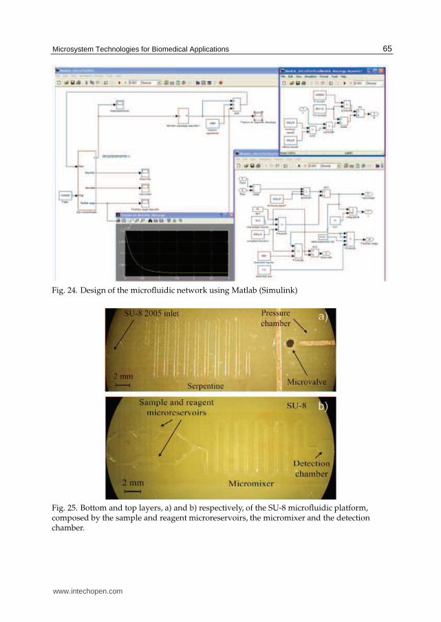
Fig. 25. Bottom and top layers, a) and b) respectively, of the SU-8 microfluidic platform,composed by the sample and reagent microreservoirs, the micromixer and the detectionchamber.
65Microsystem Technologies for Biomedical Applications
www.intechopen.com
22 Biomedical Engineering, Trends, Researches and Technologies
the copper microlines, the photodiode will receive the light emitted by the LED through thedetection chamber, generating a measurable electric current proportional to the intensity ofthe light.
6. Summary
This chapter has summarized design concepts, manufacturing processes and integration ofMEMS devices for the realization of complex microfluidic systems. These implementationsare based on polymer technology that enables the low cost and rapid prototyping ofbiomedical applications. The initial introduction has described the overall objectives andincludes a comparison between the standard silicon MEMS technology and the polymericone, remarking the facility of use and low cost of the latter. A review of standard processesusing the most common materials, PDMS and SU-8, has been described in detail in section2. The basic steps include deposition, photolithography, baking, and development. Themachinery needed for the described processes are a photoplotter to print acetate masks,a spin-coater, a photolithography machine with mask aligner, a hot-plate and a chemicalbank for polymer development. This machinery is available to the scientific community ata very reasonable cost compared to the significantly more expensive silicon technologies.Based on the previous basic manufacturing processes, a set of microfluidic devices have beenintroduced. A one-shot pneumatic impulsion device has been studied in section 3 due to itsrelevance in microfluidic systems, because it avoids the use of external pumps and complexmicrofluidic interfaces. Other devices, such as valves and flow regulators are also describedin section 5. All these devices make use of a PCB as substrate to facilitate its integration withcomplementary electronic circuitry. These devices, together with many other that are foundin literature, can be integrated to perform more complex microfluidic systems. Modeling anew fluidic design by means of the EC theory and simple simulation software allows the fastdesign of autonomous pneumatic microfluidic systems, also providing an easy design toolfor a wide variety of pressure driven LOC devices, considerably reducing the prototypingand development time. An example of a microfluidic system modeling has been developedin section 5. Finally, an example of a basic LOC including an impulsion device, a mixer anda reaction chamber has been fabricated. The final device requires 0.35J of electrical energysupplied to activate the impulsion device, with a pressure of 3 bar stored in the chamber inorder to assure the complete filling of the detection chamber by the fluid to be analyzed. Thetotal time to implement such a system is only one day, thus facilitating a fast improvementof the designs. This example can be easily generalized to implement much more complexmicrofluidic systems.
7. References
Abgrall, P., Charlot, S., Fulcrand, R., Paul, L., Boukabache, A. & Gue, A. (2008). Low-stressfabrication of 3d polymer free standing structures using lamination of photosensitivefilms,Microsyst. Technol. 14(8): 1205–1214.
Aracil, C., Perdigones, F., Moreno, J. M. & Quero, J. M. (2010). BETTS: bonding, exposing andtransferring technique in SU-8 for microsystems fabrication, Journal of Micromechanicsand Microengineering 20: 035088.
Aracil, C., Quero, J. M., Luque, A., Moreno, J. M. & Perdigones, F. (2010). Pneumatic impulsiondevice for microfluidic systems, Sensors and Actuators A: Physical vol. 163, issue 1: pp.247–254.
66 Biomedical Engineering Trends in Electronics, Communications and Software
www.intechopen.com
Microsystem Technologies for Biomedical Applications 23
Baek, J. Y., Park, J. Y., Ju, J. I., Lee, T. S. & Lee, S. H. (2005). A pneumatically controllableflexible and polymeric microfluidic valve fabricated via in situ development, Journalof Micromechanics and Microengineering 15(5): 1015.
Bruus, H. (2001). Theoretical Microfluidics, McGraw-Hill.Chuang, Y.-J., Tseng, F.-G., Cheng, J.-H. & Lin, W.-K. (2003). A novel fabrication method of
embedded micro-channels by using SU-8 thick-film photoresists, Sens. Actuators A,Phys. 103(1-2): 64 – 69.
Chung, C. & Allen, M. (2005). Uncrosslinked SU-8 as a sacrificial material, J. Micromech.Microeng. 15(1): 113–121.
Dean, R. N. & Luque, A. (2009). Applications of microelectromechanical systems in industrialprocesses and services, 56: 913–925.
Duffy, D., McDonald, J. C., Schueller, O. & Whitesides, G. M. (1998). Rapid prototyping ofmicrofluidic systems in poly(dimethylsiloxane), Anal. Chem. 70(23): 4974 – 4984.
Eddings, M. A., Johnson, M. A. & Gale, B. K. (2008). Determining the optimal PDMSPDMS bonding technique for microfluidic devices, Journal of Micromechanics andMicroengineering 18: 067001.
Ezkerra, A., Fernandez, L. J., Mayora, K. & Ruano-Lopez, J. M. (2007). Fabrication ofSU-8 free-standing structures embedded in microchannelsfor microfluidic control,J. Micromech. Microeng. 17(11): 2264–2271.
Guerin, L., Bossel, M., Demierre, M., Calmes, S. & Renaud, P. (1997). Simple and low costfabrication of embedded micro-channels by using a new thick-film photoplastic,TRANSDUCERS ’97. International Conference on Solid State Sensors and Actuators,Chicago, Vol. 2, pp. 1419–1422.
Haefliger, D. & Boisen, A. (2006). Three-dimensional microfabrication in negative resist usingprinted masks, J. Micromech. Microeng. 16(5): 951–957.
Henry, S., McAllister, D. V., Allen, M. G. & Prausnitz, M. R. (1998). Micromachinedneedles for the transdermal delivery of drugs, Proceedings of the IEEE Eleventh AnnualInternational Workshop on Micro Electro Mechanical Systems, Heidelberg, Germany,pp. 494–498.
Hong, C. C., Choi, J. W. & Ahn, C. H. (2007). An on-chip air-bursting detonator fordriving fluids on disposable lab-on-a-chip systems, Journal of Micromechanics andMicroengineering 17: 410–417.
Huang, H. & Fu, C. (2007). Different fabrication methods of out-of-plane polymer hollowneedle arrays and their variations, J. Micromech. Microeng. 17: 393–402.
Koch, C., Remcho, V. & Ingle, J. (2009). Chemical,pdms and tubing-based peristalticmicropumps with direct actuation, Sensors and Actuators B: Chemical 135(2): 664–670.
Kovacs, G. T. A., Maluf, N. I. & Petersen, K. E. (1998). Bulk micromachining of silicon,86(8): 1536–1551.
Laser, D. J. & Santiago, J. G. (2004). A review of micropumps, Journal of Micromechanics andMicroengineering 14: R35–R64.
Lim, Y. C., Kouzani, A. Z., & Duan, W. (2010). Lab-on-a-chip: a component view, Microsyst.Technol. 16:1995-2015.
Lorenz, H., Despont, M., Fahrni, N., LaBianca, N., Renaud, P. & Vettiger, P. (1997). SU-8:a low-cost negative resist for MEMS, Journal of Micromechanics and Microengineering7: 121–124.
Mata, A., Fleischman, A. J. & Roy, S. (2006). Fabrication of multi-layer su-8 microstructures,Journal of Micromechanics and Microengineering 16: 276–284.
67Microsystem Technologies for Biomedical Applications
www.intechopen.com
24 Biomedical Engineering, Trends, Researches and Technologies
McDonald, J. C. & Whitesides, G. M. (2002). Poly(dimethylsiloxane) as a material forfabricating microfluidic devices, Accounts of Chemical Research 35(7): 491 – 499.
Metz, S., Jiguet, S., Bertsch, A., & Renaud. (2004). Polyimide and SU-8 microfluidicdevices manufactured by heat-depolymerizable sacrificial material technique, LabChip 4:114-120.
Moreno, J. M. & Quero, J. M. (2010). A novel single-use SU-8 microvalve for pressure-drivenmicrofluidic applications, Journal of Micromechanics and Microengineering 20: 015005.
Moreno, M., Aracil, C. & Quero, J. (2008). High-integrated microvalve for lab-on-chipbiomedical applications, pp. 313 –316.
Murillo, G.,Davis, Z. J., Keller, S., Abadal, G., Agusti, J., Cagliani, A., Noeth, N., Boisen, A.& Barniol, N. (2010). Novel SU-8 based vacuum wafer-level packaging for MEMSdevices,Microelectronic Engineering 87:1173-1176.
Oh, K. W. & Ahn, C. H. (2006). A review of microvalves, Journal of Micromechanics andMicroengineering 16: R13–R39.
Patel, J. N., Kaminska, B., Gray, B. L. & Gates, B. D. (2008). Pdms as a sacrificial substratefor SU-8-based biomedical and microfluidic applications, J. Micromech. Microeng.18(9): 095028 (11pp).
Perdigones, F., Luque, A. & Quero, J. M. (2010a). Novel structure for a pneumaticallycontrolled flow regulator with positive gain, Journal of Microelectromechanical Systems.19(5): 1070 – 1078.
Perdigones, F., Luque, A. & Quero, J. M. (2010b). PDMS microdevice for precise liquidaspiration in the submicroliter range based on the Venturi effect, MicroelectronicEngineering 87(11): 2103 – 2109.
Perdigones, F., Moreno, J. M., Luque, A. & Quero, J. M. (2010). Characterisation of thefabrication process of freestanding SU-8 microstructures integrated in printing circuitboard in microelectromechanical systems,Micro and Nano Letters 5: 7–13.
Perdigones, F., Luque, A. & Quero, J. M. (In press). Highly integrable flow regulator withpositive gain, Journal of Microelectromechanical Systems In press.
Petersen, K. E. (1982). Silicon as a mechanical material, 70(5): 420–457.Roark, R. J., Budynas, R. G. & Young, W. C. (2001). Roark’s Formulas for stress and strain,
McGraw-Hill.Status of the MEMS industry (2008). Yole Dveloppement.Takao, H. & Ishida, M. (2003). Microfluidic integrated circuits for signal processing using
analogous relationship between pneumatic microvalve and MOSFET, Journal ofMicroelectromechanical Systems 12(4): 497–505.
Vedel, S. (2009). Millisecond dynamics in microfluidics: Equivalent circuit theory and experiment,PhD thesis, DTU Nanotech, Department of Micro and Nanotechnology.
68 Biomedical Engineering Trends in Electronics, Communications and Software
www.intechopen.com

Biomedical Engineering, Trends in Electronics, Communicationsand SoftwareEdited by Mr Anthony Laskovski
ISBN 978-953-307-475-7Hard cover, 736 pagesPublisher InTechPublished online 08, January, 2011Published in print edition January, 2011
InTech EuropeUniversity Campus STeP Ri Slavka Krautzeka 83/A 51000 Rijeka, Croatia Phone: +385 (51) 770 447 Fax: +385 (51) 686 166www.intechopen.com
InTech ChinaUnit 405, Office Block, Hotel Equatorial Shanghai No.65, Yan An Road (West), Shanghai, 200040, China
Phone: +86-21-62489820 Fax: +86-21-62489821
Rapid technological developments in the last century have brought the field of biomedical engineering into atotally new realm. Breakthroughs in materials science, imaging, electronics and, more recently, the informationage have improved our understanding of the human body. As a result, the field of biomedical engineering isthriving, with innovations that aim to improve the quality and reduce the cost of medical care. This book is thefirst in a series of three that will present recent trends in biomedical engineering, with a particular focus onapplications in electronics and communications. More specifically: wireless monitoring, sensors, medicalimaging and the management of medical information are covered, among other subjects.
How to referenceIn order to correctly reference this scholarly work, feel free to copy and paste the following:
Francisco Perdigones, Jose Miguel Moreno, Antonio Luque, Carmen Aracil and Jose Quero (2011).Microsystem Technologies for Biomedical Applications, Biomedical Engineering, Trends in Electronics,Communications and Software, Mr Anthony Laskovski (Ed.), ISBN: 978-953-307-475-7, InTech, Availablefrom: http://www.intechopen.com/books/biomedical-engineering-trends-in-electronics-communications-and-software/microsystem-technologies-for-biomedical-applications

© 2011 The Author(s). Licensee IntechOpen. This chapter is distributedunder the terms of the Creative Commons Attribution-NonCommercial-ShareAlike-3.0 License, which permits use, distribution and reproduction fornon-commercial purposes, provided the original is properly cited andderivative works building on this content are distributed under the samelicense.