MICRONAS CDC 3231G-C Automotive Controllerdatasheet.elcodis.com/pdf2/88/31/883198/cdc3231g-c.pdfCDC...
36
CDC 3231G-C Automotive Controller Edition June 30, 2003 6251-609-2AI ADVANCE INFORMATION MICRONAS MICRONAS
Transcript of MICRONAS CDC 3231G-C Automotive Controllerdatasheet.elcodis.com/pdf2/88/31/883198/cdc3231g-c.pdfCDC...

CDC 3231G-CAutomotive Controller
Edition June 30, 20036251-609-2AI
ADVANCE INFORMATION
MICRONAS
MICRONAS

CDC 3231G-C ADVANCE INFORMATION
2 June 30, 2003; 6251-609-2AI Micronas
Contents
Page Section Title
3 1. Introduction3 1.1. Features5 1.2. Abbreviations6 1.3. Block Diagram
7 2. Packages and Pins7 2.1. Package Outline Dimensions8 2.2. Pin Assignment8 2.3. Pin Function Description
(differing from document “CDC32xxG-C Automotive Controller - Family User Manual,CDC3205G-C Automotive Controller” (6251-579-1PD))
9 2.4. External Components
11 3. Electrical Data11 3.1. Absolute Maximum Ratings12 3.2. Recommended Operating Conditions13 3.3. Characteristics15 3.4. Recommended Quartz Crystal Characteristics
17 4. CPU and Clock System
19 5. Memory and Special Function ROM (SFR) System
21 6. Core Logic21 6.1. Control Word (CW)
23 7. IRQ Interrupt Controller Unit (ICU)
25 8. Hardware Options25 8.1. Functional Description
27 9. Register Cross Reference Table27 9.1. 8-Bit I/O Region32 9.2. 32-Bit I/O Region33 9.3. Modified Registers
35 10. Differences
36 11. Data Sheet History

ADVANCE INFORMATION CDC 3231G-C
1. Introduction
Release Note: Revision bars indicate significantchanges to the previous edition.
The device is a microcontroller for use in automotive applica-tions. The on-chip CPU is an ARM processor ARM7TDMI
with 32-bit data and address bus, which supports Thumb
format instructions.
The chip contains timer/counters, interrupt controller, multichannel AD converter, stepper motor and LCD driver, CAN
interfaces and PWM outputs and a crystal clock multiplyingPLL.
This document provides ROM hardware specific information.General information on operating the IC can be found in thedocument “CDC32xxG-C Automotive Controller - FamilyUser Manual, CDC3205G-C Automotive Controller” (6251-579-1PD).
1.1. Features
Table 1–1: CDC32xxG-C Family Feature List
This Device:
Item CDC3205G-CEMU
CDC3207G-CMCM Flash
CDC3272G-CMask ROM
CDC3231G-CMask ROM
Core
CPU 32-bit ARM7TDMI
CPU-Active Operation Modes DEEP SLOW, SLOW, FAST and PLL
Power Saving Modes (CPU Inactive) IDLE, WAKE and STANDBY
CPU clock multiplication PLL delivering up to 50MHz
EMI Reduction Mode selectable in PLL mode
Oscillators 4 to 5MHz Quartz and 20 to 50kHz Internal RC
RAM, zero wait state, 32 bit wide 32kByte 16kByte 6kByte
ROM ROMless, ext.up to4M x 32/8M x 16,int. 8-KByteBoot ROM
512-kByte Flash(256K x 16) topboot conf.,int. 8-KByteBoot ROM
384kByte(96K x 32/192K x 16)
128kByte(32K x 32/64K x 16)
Digital Watchdog ✔
Central Clock Divider ✔
Interrupt Controller expanding IRQ 40 inputs, 16 priority levels 26 inputs, 16priority levels
Port Interrupts including Slope Selection 6 inputs 5 inputs
Port Wake-Up Inputs including Slope / LevelSelection
10 inputs
Patch Module 10 ROM locations
Boot System allows in-system downloading ofexternal code to Flash memory viaJTAG
-
Micronas June 30, 2003; 6251-609-2AI 3

CDC 3231G-C ADVANCE INFORMATION
Device Lock Module Inhibits Access to internal Firm-ware, Lock settable by Customer
-
Analog
Reset/Alarm Combined Input for Regulator Input Supervision
Clock and Supply Supervision ✔
10-bit ADC, charge balance type 16 channels (each selectable as digital input)
ADC Reference VREF Pin, P1.0 Pin, P1.1 Pin or VREFINT Internal Bandgap selectable
Comparators P06COMP with 1/2 AVDD reference,WAITCOMP with Internal Bandgap reference
LCD Internal processing of all analog voltages for the LCD driver
Communication
DMA 3 DMA Channels, one each for serving the GraphicsBus interface, SPI0 and SPI1
-
UART 2: UART0 and UART1 UART0
Synchronous Serial Peripheral Interfaces 2: SPI0 and SPI1, DMA supported
Full CAN modules V2.0Bwith 512-byte object RAM each(LCAN000E)
4: CAN0, CAN1, CAN2 and CAN3 2: CAN0 andCAN1
1: CAN0
DIGITbus 1 master module -
I2C 2 master modules: I2C0 and I2C1 I2C0
Graphics Bus Interface 8-bit data bus, DMA supported, e.g. for connection ofEPSON SED 1560 LCD controller
-
Input & Output
Universal Ports selectable as 4:1 mux LCDSegment/Backplane lines or Digital I/O Ports
up to 52 I/O or 48 LCD segment lines (=192 segments),individually configurable as I/O or LCD
up to 50 I/O or46LCD seg-ment lines(=184 seg-ments)
Universal Port Slew Rate SW selectable
Stepper Motor Control Modules with High-Current Ports
7 Modules,32 dI/dt controlled ports
4 Modules23 dI/dt con-trolled ports
PWM Modules, each configurable as two 8-bit PWMs or one 16-bit PWM
6 Modules: PWM0/1, PWM2/3, PWM4/5, PWM6/7,PWM8/9 and PWM10/11
5 Modules:PWM0/1,PWM2/3,PWM4/5,PWM6/7,PWM8/9
Phase-Frequency Modulator 2: PFM0 and PFM1 -
Audio Module with auto-decay ✔
Table 1–1: CDC32xxG-C Family Feature List, continued
This Device:
Item CDC3205G-CEMU
CDC3207G-CMCM Flash
CDC3272G-CMask ROM
CDC3231G-CMask ROM
4 June 30, 2003; 6251-609-2AI Micronas

ADVANCE INFORMATION CDC 3231G-C
ARM and Thumb are the registered trademarks of ARM Limited.ARM7TDMI is the trademark of ARM Limited.
1.2. Abbreviations
ADC Analog-to-Digital ConverterAM Audio ModuleCAN Controller Area Network ModuleCAPCOM Capture/Compare ModuleCCC Capture/Compare CounterCPU Central Processing UnitDMA Direct Memory Access ModuleERM EMI Reduction ModeETM Embedded Trace ModuleICU Interrupt ControllerI2C I2C Interface Module
LCD Liquid Crystal Display ModuleP06COMP P0.6 Alarm ComparatorPINT Port Interrupt ModulePWM Pulse Width Modulator ModuleSM Stepper Motor Control ModuleSPI Serial Synchronous Peripheral InterfaceT TimerUART Universal Asynchronous Receiver TransmitterWAITCOMP Wait Comparator
SW selectable Clock outputs 2
Polling / Flash Timer Output 1 High-Current Port output operable in Power Saving Modes
Timers & Counters
16-bit free running counters with Capture/Compare modules
CCC0 with 4 CAPCOMCCC1 with 2 CAPCOM
CCC0 with 4CAPCOM
16-bit timers 1: T0
8-bit timers 4: T1, T2, T3 and T4
Real Time Clock, Delivering Hours, Minutesand Seconds
✔
Miscellaneous
Scalable layout in CAN, RAM and ROM - ✔
Various randomly selectable HW options Set by copy from user program storage during system start-up
JTAG test interface ✔ allows Flashprogramming
✔
On Chip Debug Aids EmbeddedTrace Module,JTAG
JTAG
Core Bond-Out ✔ -
Supply Voltage 3.5 to 5.5V (limited I/O performance below 4.5V)
Case Temperature Range 0 to +70C -40 to +105C
Package
Type Ceramic257PGA
Plastic 128QFP0.5mm pitch
Bonded Pins 256 128 126 111
Table 1–1: CDC32xxG-C Family Feature List, continued
This Device:
Item CDC3205G-CEMU
CDC3207G-CMCM Flash
CDC3272G-CMask ROM
CDC3231G-CMask ROM
Micronas June 30, 2003; 6251-609-2AI 5

CDC 3231G-C ADVANCE INFORMATION
1.3. Block Diagram
Fig. 1–1: CDC3231G-C block diagram
4
3
8
8
7
8
4
3
2
4
4
XTAL1XTAL2
TEST
RESETQ
VREFAVDDAVSS
HVDD0HVSS0
5
Brid
ge
Bridge
8Bit Timer 4
8Bit Timer 3
8Bit Timer 2
8Bit Timer 1
16Bit Timer 0
8Bit PWM 0
8/16B PWM 1
8
HVDD1HVSS1
WAITWAITH
TEST2
32 16/32
8
4
8
6
8Bit PWM 2
8/16B PWM 3
8Bit PWM 4
8/16B PWM 5
8Bit PWM 6
8/16B PWM 7
8Bit PWM 8
8/16B PWM 9
2.5V Reg.
UVDD VDDUVSS VSS
BVDD
2.5V Reg.
HP
ort0
HP
ort2
HP
ort3
HP
ort4
HP
ort5
HP
ort7
4
4
PP
ort0
PP
ort1
PP
ort2
2
MemoryController
VREFINT
PLL/ERM
RC Oscillator
RTC
Test
Reset/Alarm
WatchdogClock
PowerSaving
JTAG Testand DebugInterface
CAPCOM 0
CAPCOM 1
CAPCOM 2
CAPCOM 3
16Bit CCC 0
UP
ort8
UP
ort0
UP
ort1
UP
ort2
UP
ort3
UP
ort4
UP
ort5
UP
ort6
UP
ort7
UART 0
SPI 0
SPI 1
CAN 0
I2C 0
LCD Control
Audio Module
Clock Out 0
Clock Out 1
Wait Comp.
P06 Comp.
Bandgap Ref.
10Bit ADC
ARM7TDMICPU
26 InputInterrupt
Controller
SRAM
Stepper MotorControl
Patch
SFR4k x 16
ROM32k x 32
1.5k x 32
10 Locations
6 June 30, 2003; 6251-609-2AI Micronas

ADVANCE INFORMATION CDC 3231G-C
2. Packages and Pins2.1. Package Outline Dimensions
Fig. 2–1:PMQFP128-2: Plastic Metric Quad Flat Package, 128 leads, 14 × 20 × 2.7 mm3
Ordering code: QKWeight approximately 1.81 g
Micronas June 30, 2003; 6251-609-2AI 7

CDC 3231G-C ADVANCE INFORMATION
2.2. Pin Assignment
Fig. 2–1: Pin Assignment. Please note that in contrast to CDC3205G-C, CDC3207G-C and CDC3272G-C the function CC3-OUT is not present on pin 104!
2.3. Pin Function Description(differing from document “CDC32xxG-C Automotive Controller - Family User Manual, CDC3205G-C Automotive Controller”
(6251-579-1PD))
TEST2For normal operation with internal code connect TEST2 to
System Ground (no internal pull-down).
Pin Functions Note
PinNo.LCD
ModePortSpecial Out
PortSpecial In
BasicFunction
SEG3.1 CC1-OUT CC1-IN / TMS U3.1 116SEG3.0 CC2-OUT CC2-IN / TDI U3.0 117
TEST2 118UVDD 119UVSS 120
SEG2.6 U2.6 121SEG2.5 CC1-OUT UART0-RX U2.5 122SEG2.4 UART0-TX CC1-IN U2.4 123SEG2.3 CC2-OUT U2.3 124SEG2.2 CC2-IN U2.2 125SEG7.7 CO0 U7.7 126SEG7.6 CO1 U7.6 127SEG7.5 LCK U7.5 128SEG7.4 U7.4 1
NC 2NC 3NC 4
SEG5.2 U5.2 5SEG5.1 U5.1 6SEG5.0 U5.0 7SEG2.1 SDA0 WP6/SDA0/CAN0-RX U2.1 8SEG2.0 SCL0/CAN0-TX SCL0 U2.0 9SEG1.7 WP0/PINT0 U1.7 10SEG1.6 INTRES/CO0 PINT1 U1.6 11SEG1.5 CO1/CO0Q PINT2 U1.5 12
TEST 13RESETQ/ALARMQ 14
XTAL2 15XTAL1 16
VSS 17VDD 18
SEG1.4 ITSTOUT/AM-OUT U1.4 19SEG1.3 MTO/AM-PWM WP3 U1.3 20SEG1.2 INTRES/T0-OUT MTI/ITSTIN U1.2 21SEG1.1 T1-OUT U1.1 22SEG1.0 T2-OUT U1.0 23SEG0.7 T3-OUT WP4 U0.7 24SEG0.6 CC3-OUT/T4-OUT CC3-IN U0.6 25SEG0.5 CC3-OUT U0.5 26SEG0.4 CO1 PINT5 U0.4 27SEG0.3 PWM0 U0.3 28SEG0.2 PWM1 U0.2 29SEG0.1 PWM2 U0.1 30SEG0.0 PWM3 U0.0 31
PWM4 H7.3 32PWM6 H7.2 33PWM8 H7.1 34PWM9 H7.0 35
NC 36NC 37NC 38NC 39NC 40NC 41
SMD1+ SMD-COMP3 H5.3 42SMD1- SMD-COMP2 H5.2 43
HVDD0 44HVSS0 45
SMD2+ SMD-COMP1 H5.1 46SMD2- SMD-COMP0 H5.0 47SMA1+ SMA-COMP3 H4.3 48SMA1- SMA-COMP2 H4.2 49SMA2+ SMA-COMP1 H4.1 50SMA2- SMA-COMP0 H4.0 51
PinNo.
Note
Pin FunctionsBasicFunction
PortSpecial In
PortSpecial Out
LCDMode
115 U3.2 CC0-IN / TCK CC0-OUT SEG3.2114 U3.3 CO0/TDO SEG3.3113 U3.4 SPI0-CLK-IN SPI0-CLK-OUT SEG3.4112 U3.5 SPI0-D-IN TO3 SEG3.5111 U3.6 SPI0-D-OUT SEG3.6110 U3.7 SPI1-CLK-IN SPI1-CLK-OUT SEG3.7109 U4.0 SPI1-D-IN CC0-OUT BP0108 U4.1 CC0-IN SPI1-D-OUT BP1107 U4.2 CAN0-TX BP2106 U4.3 CAN0-RX/WP5 TO2 BP3105 U8.0 SEG8.0104 U8.1 SEG8.1103 U8.2 LCD-CLK-IN SEG8.2102 U8.3 WP9 LCD-CLK-OUT SEG8.3101 U8.4 LCD-SYNC-IN SEG8.4100 U8.5 PINT3/WP8 LCD-SYNC-OUT SEG8.599 NC98 U6.1 WP7 SEG6.197 U6.2 SEG6.296 P2.095 P2.194 P0.093 P0.192 P0.291 P0.390 P0.489 P0.588 P0.6 P0.6 Comp.87 P0.786 WAITH85 WAIT84 BVDD83 AVSS82 AVDD81 VREFINT80 VREF79 P1.0 VREF0/WP178 P1.1 VREF1/WP277 P1.2 PINT076 P1.3 PINT175 P1.4 PINT274 P1.5 PINT373 P1.672 P1.7 PINT571 H0.0 PWM770 H0.1 PWM569 H0.2 PWM3/POL68 NC67 NC66 NC65 NC64 NC63 NC62 NC61 H2.0 SMC-COMP0 SMC2-60 H2.1 SMC-COMP1 SMC2+59 HVSS158 HVDD157 H2.2 SMC-COMP2 SMC1-56 H2.3 SMC-COMP3 SMC1+55 H3.0 SMB-COMP0 SMB2-54 H3.1 SMB-COMP1 SMB2+53 H3.2 SMB-COMP2 SMB1-52 H3.3 SMB-COMP3 SMB1+
1
38
102
65
39 64
103128 116 115
5251
NC = not connected,leave vacant(...) = future usage
8 June 30, 2003; 6251-609-2AI Micronas
ADVANCE INFORMATION CDC 3231G-C
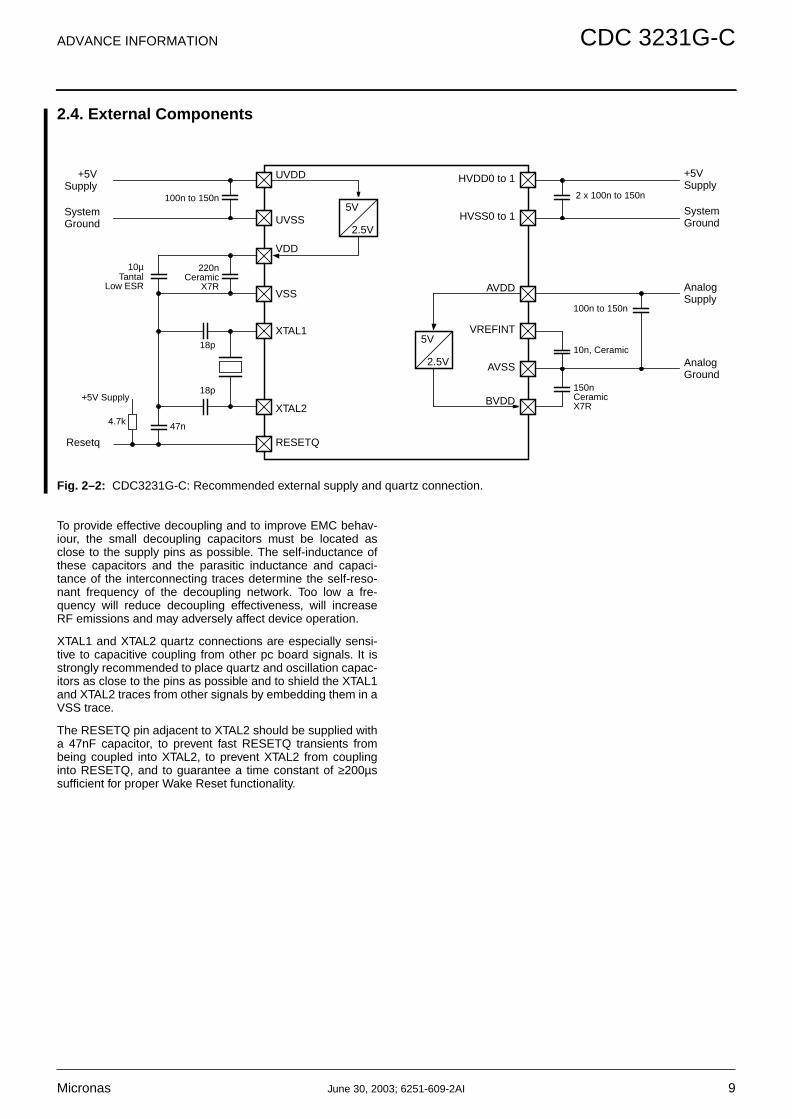
2.4. External Components
Fig. 2–2: CDC3231G-C: Recommended external supply and quartz connection.
To provide effective decoupling and to improve EMC behav-iour, the small decoupling capacitors must be located asclose to the supply pins as possible. The self-inductance ofthese capacitors and the parasitic inductance and capaci-tance of the interconnecting traces determine the self-reso-nant frequency of the decoupling network. Too low a fre-quency will reduce decoupling effectiveness, will increaseRF emissions and may adversely affect device operation.
XTAL1 and XTAL2 quartz connections are especially sensi-tive to capacitive coupling from other pc board signals. It isstrongly recommended to place quartz and oscillation capac-itors as close to the pins as possible and to shield the XTAL1and XTAL2 traces from other signals by embedding them in aVSS trace.
The RESETQ pin adjacent to XTAL2 should be supplied witha 47nF capacitor, to prevent fast RESETQ transients frombeing coupled into XTAL2, to prevent XTAL2 from couplinginto RESETQ, and to guarantee a time constant of ≥200µssufficient for proper Wake Reset functionality.
SystemGround
+5VSupply
2 x 100n to 150n5V
2.5V
5V
2.5V
VREFINT
AVSS
AVDD
BVDD
AnalogGround
AnalogSupply
150nCeramic
10n, Ceramic
VDD
VSS
XTAL1
XTAL2
UVSS
UVDD
SystemGround
+5VSupply
220nCeramic
10µ
18p
18p
100n to 150n
100n to 150n
TantalLow ESR X7R
X7R
HVDD0 to 1
HVSS0 to 1
RESETQResetq
4.7k
+5V Supply
47n
Micronas June 30, 2003; 6251-609-2AI 9

CDC 3231G-C ADVANCE INFORMATION
10 June 30, 2003; 6251-609-2AI Micronas

ADVANCE INFORMATION CDC 3231G-C
3. Electrical Data
3.1. Absolute Maximum Ratings
Stresses beyond those listed in the “Absolute Maximum Ratings” may cause permanent damage to the device. This is a stressrating only. Functional operation of the device at these conditions is not implied. Exposure to absolute maximum ratings condi-tions for extended periods will affect device reliability.
This device contains circuitry to protect the inputs and outputs against damage due to high static voltages or electric fields; how-ever, it is advised that normal precautions be taken to avoid application of any voltage higher than absolute maximum-rated volt-ages to this high-impedance circuit.
1) This condition represents the worst case load with regard to the intended application
Table 3–1: All voltages listed are referenced to ground (UVSS=HVSSn=AVSS=0V), except where noted. All grounds except VSSmust be connected externally low-ohmic.
Symbol Parameter Pin Name Min. Max. Unit
VSUP Main Supply VoltageAnalog Supply VoltageSM Supply Voltage
UVDDAVDDHVDDn
-0.3 6.0 V
VREG Core Supply VoltagePLL Supply Voltage
VDDBVDD
-0.3 3.0 V
ISUP Core Supply CurrentMain Supply Current
VDD, VSS,UVDD, UVSS
-100 100 mA
Analog Supply Current AVDD, AVSS -20 20 mA
SM Supply Current@TCASE=105C, Duty Factor=0.71 1)
HVDDnHVSSn
-250 250 mA
PLL Supply Current BVDD -20 20 mA
Vin Input Voltage U-Ports,XTAL,RESETQ,TEST, TEST2
UVSS-0.5 UVDD+0.7 V
P-PortsVREF
UVSS-0.5 AVDD+0.7 V
H-Ports HVSS-0.5 HVDD+0.7 V
Iin Input Current all Inputs 0 2 mA
Io Output Current U-Ports,RESETQ, WAITH
-5 5 mA
H-Ports -60 60 mA
toshsl Duration of Short Circuit to UVSS orUVDD, Port SLOW Mode enabled
U-Ports, except inDP Mode
indefinite s
Tj Junction Temperature under Bias -45 115 °C
Ts Storage Temperature -45 125 °C
Pmax Maximum Power Dissipation 0.8 W
Micronas June 30, 2003; 6251-609-2AI 11

CDC 3231G-C ADVANCE INFORMATION
3.2. Recommended Operating Conditions
Do not insert the device into a live socket. Instead, apply power by switching on the external power supply.
Keep UVDD=AVDD during all power-up and power-down sequences.
Failure to comply with the above recommendations will result in unpredictable behavior of the device and may result in devicedestruction.
Functional operation of the device beyond those indicated in the “Recommended Operating Conditions” of this specification is notimplied, may result in unpredictable behaviour of the device and may reduce reliability and lifetime.
Table 3–2: All voltages listed are referenced to ground (UVSS=HVSSn=AVSS=0V), except where noted. All grounds except VSSmust be connected externally low-ohmic.
Symbol Parameter Pin Name Min. Typ Max. Unit
VSUP Main Supply VoltageAnalog Supply Voltage
UVDD=AVDD 3.5 5 5.5 V
HVSUP SM Supply Voltage HVDDn 4.75 5 5.25 V
dVDD Ripple, Peak to Peak UVDDAVDDBVDDVDD
200 mV
dVDD/dt Supply Voltage Up/Down RampingRate
UVDDAVDD
20 V/µs
fXTAL XTAL Clock Frequency XTAL1 4 4 5 MHz
fSYS CPU Clock Frequency, PLL on For a list of available settings see Tables 4–1 and4–2.
fBUS Program Storage Clock Fre-quency, PLL on
Vil(see Table 2-2for a list of inputtypes and theirsupply volt-ages)
Automotive Low Input Voltage U-PortsH-PortsP-Ports
0.5*xVDD V
CMOS Low Input Voltage U-Ports, TEST,TEST2H-PortsP-Ports
0.3*xVDD V
Vih(see Table 2-2for a list of inputtypes and theirsupply volt-ages)
Automotive High Input Voltage U-PortsH-PortsP-Ports
0.86*xVDD V
CMOS High Input Voltage U-Ports,TEST,TEST2H-PortsP-Ports
0.7*xVDD V
RVil Reset Active Input Voltage RESETQ 0.75 V
WRVil Reset Active Input Voltage duringPower Saving Modes and WakeReset
RESETQ 0.4 V
RVim Reset Inactive and Alarm ActiveInput Voltage
RESETQ 1.5 2.3 V
RVih Reset Inactive and Alarm InactiveInput Voltage
RESETQ 3.2 V
WRVih Reset Inactive Input Voltage dur-ing Power Saving Modes andWake Reset
RESETQ UVDD-0.4V V
12 June 30, 2003; 6251-609-2AI Micronas

ADVANCE INFORMATION CDC 3231G-C
3.3. Characteristics
Listed are only those characteristics that are differing from Chapter 3.3 of Document “CDC32xxG-C Automotive Controller - Fam-ily User Manual, CDC3205G-C Automotive Controller” (6251-579-1PD). All not differing characteristics, that are not listed here,apply, but in a TCASE temperature range extended to -40 to +105C
VREFi Ext. ADC Reference Input Voltage VREF 2.56 AVDD V
PVi ADC Port Input Voltage referencedto int. VREF Reference
ADC Port Input Voltage referencedto ext. VREFINT Reference
P-Ports 0
0
VREFi
VREFINT
V
Table 3–3: UVSS=HVSSn=AVSS=0V, 3.5V<AVDD=UVDD<5.5V, 4.75V<HVDDn<5.25V, TCASE=-40 to +105C, fXTAL=5MHz, externalcomponents according to Fig. 2–3 (unless otherwise noted)
Symbol Parameter Pin Na. Min. Typ 1) Max. Unit Test Conditions
Package
Rthjc Thermal Resistance fromJunction to Case
6 C/W measured on Micronastypical 2-layer board,1s1p, described in docu-ment “Integrated Circuits- Thermal Characteriza-tion of Packages” (6200-266-1E) (modifiedJESD-51.3)
Rthja Thermal Resistance fromJunction to Ambient
50 C/W
Supply Currents (CMOS levels on all inputs, i.e. Vil=xVSS±0.3V and Vih=xVDD±0.3V, no loads on outputs)
UIDDp UVDD PLL Mode SupplyCurrent
UVDD 50 mA fSYS=24MHz
UIDDf UVDD FAST Mode SupplyCurrent
UVDD 22 mA all Modules off, 2)
UIDDs UVDD SLOW Mode SupplyCurrent
UVDD seeFig. 3–1
1.4 mA all Modules off 2) 3)
UIDDd UVDD DEEP SLOW ModeSupply Current
UVDD seeFig. 3–1
0.9 mA all Modules off 3)
UIDDw UVDD WAKE Mode SupplyCurrent
UVDD 0 20 50 µA RC and XTAL oscillatorsoff
UIDDst UVDD STANDBY ModeSupply Current
UVDD 35 75 µA RC oscillator on, XTALoff
UVDD 60 100 µA XTAL oscillator on, RCoff 3)
1) Typical values describe typical behaviour at room temperature (25C, unless otherwise noted), with typicalRecommended Operating Conditions applied, and are not 100% tested.
Table 3–2: All voltages listed are referenced to ground (UVSS=HVSSn=AVSS=0V), except where noted. All grounds except VSSmust be connected externally low-ohmic.
Symbol Parameter Pin Name Min. Typ Max. Unit
Micronas June 30, 2003; 6251-609-2AI 13
CDC 3231G-C ADVANCE INFORMATION
2) Value may be exceeded with unusual Hardware Option setting
3) Measured with external clock. Add typically 120µA for operation on quartz with SR0.XTAL=0 (Oscillator RUN mode).
Fig. 3–1: Typical UIDD characteristics over temperature @ fXTAL=4MHz, 5V
UIDDi UVDD IDLE Mode SupplyCurrent
UVDD 50 TBD µA RC oscillator on, XTALoff
75 TBD µA XTAL oscillator on, RCoff 3)
AIDDa AVDD Active Supply Cur-rent
AVDD 0.35 0.6 mA ADC on, PLL off
1 2 mA ADC and PLL on,fSYS=24MHz
AIDDq Quiescent Supply Current AVDD 0 1 10 µA SLOW, DEEP SLOWand power savingmodes, ADC and PLL off
HIDDq Sum ofallHVDDn
0 1 40 µA no Output Activity,SM Module off
Inputs
Ii Input Leakage Current TEST2 -1 1 µA 0<Vi<UVDD
Table 3–3: UVSS=HVSSn=AVSS=0V, 3.5V<AVDD=UVDD<5.5V, 4.75V<HVDDn<5.25V, TCASE=-40 to +105C, fXTAL=5MHz, externalcomponents according to Fig. 2–3 (unless otherwise noted)
Symbol Parameter Pin Na. Min. Typ 1) Max. Unit Test Conditions
1) Typical values describe typical behaviour at room temperature (25C, unless otherwise noted), with typicalRecommended Operating Conditions applied, and are not 100% tested.
0
100
200
300
400
500
600
700
800
900
–40 –30 –20 –10 0 10 20 30 40 50 60 70 80 90 100 110 120 °C
µA
TCASE
UIDD
UIDDs (SLOW mode)
UIDDd (DEEP SLOW mode)
UIDDi (IDLE mode)
14 June 30, 2003; 6251-609-2AI Micronas

ADVANCE INFORMATION CDC 3231G-C
3.4. Recommended Quartz Crystal Characteristics
See Chapter 3.4 of document “CDC32xxG-C Automotive Controller - Family User Manual, CDC3205G-C Automotive Controller”(6251-579-1PD).
Micronas June 30, 2003; 6251-609-2AI 15
CDC 3231G-C ADVANCE INFORMATION
16 June 30, 2003; 6251-609-2AI Micronas

ADVANCE INFORMATION CDC 3231G-C
4. CPU and Clock System
4.1. Recommended Register Settings
Other settings for PMF, IOP and WSR than those given inTables 4–1 and 4–2 shall not be used and may result inundefined behaviour. It is required not to operate I/O fasterthan ROM.
Suppression Strength (SUP) and Clock Tolerance (TOL) maybe varied between zero and the values for strong settingsaccording to the rules in Section 4.4.2 of the document“CDC32xxG-C Automotive Controller - Family User Manual,CDC3205G-C Automotive Controller” (6251-579-1PD). Thegiven limits must not be exceeded.
Table 4–1: PLL and ERM Modes: Recommended Settings and Resulting Operating Frequencies (MHz)
fXTAL CPU ROM I/O ERMC.EOM = 1 ERMC.EOM = 2 or 3
Weak Normal Strong Weak Normal Strong
fSYS PLLC.PMF
fBUS WSR fIO=f0
IOC.IOP S
UP
TOL
SU
P
TOL
SU
P
TOL
SU
P
TOL
SU
P
TOL
SU
P
TOL
4 8 1 8 0x00 8 0 0 4 0 7 0 11 4 2 7 4 11 6
16 3 8 0x11 8 1 0 8 0 14 0 15 8 4 14 7 22 11
24 5 8 0x22 8 2 0 12 0 15 0 15 12 6 21 11 31 12
12 0x11 0 10 0 10 0 10 12 2 21 2 33 2
32 7 8 0x33 8 3 0 12 0 12 0 12 16 8 28 12 31 12
10.67 0x22 0 12 0 12 0 12 16 8 192328
976
192337
976
40 9 10 0x33 8 4 0 6 0 6 0 6 21 6 35 6 37 6
48 11 12 0x33 8 5 0 1 0 1 0 1 25 1 42 1 42 1
5 10 1 10 0x00 10 0 0 5 0 8 0 14 5 3 8 4 14 7
20 3 10 0x11 10 1 0 10 0 15 0 15 10 5 17 8 28 8
30 5 10 0x22 10 2 0 14 0 14 0 14 15 8 2426
1211
283035
1098
40 7 10 0x33 10 3 0 6 0 6 0 6 21 6 35 6 37 6
50 9 12.5 0x33 10 4 set ERMC.EOM=0 set ERMC.EOM=0
Table 4–2: PLL2 and ERM Modes: Settings Sacrificing Unlimited Operation of Peripheral Modules and Resulting OperatingFrequencies (MHz)
fXTAL CPU ROM I/O ERMC.EOM = 1 ERMC.EOM = 2 or 3
Weak Normal Strong Weak Normal Strong
fSYS PLLC.PMF
fBUS WSR fIO=f0
IOC.IOP S
UP
TOL
SU
P
TOL
SU
P
TOL
SU
P
TOL
SU
P
TOL
SU
P
TOL
4 12 2 6 0x11 4 2 0 6 0 10 0 15 6 3 10 5 16 8
12 0x00 0 5 0 5 0 5 6 2 10 2 16 2
20 4 10 0x11 4 4 0 10 0 15 0 15 10 5 17 8 28 8
5 15 2 7.5 0x11 5 2 0 7 0 13 0 15 7 4 13 7 21 11
Micronas June 30, 2003; 6251-609-2AI 17

CDC 3231G-C ADVANCE INFORMATION
18 June 30, 2003; 6251-609-2AI Micronas

ADVANCE INFORMATION CDC 3231G-C
5. Memory and Special Function ROM (SFR) System
Fig. 5–1: Address Map. Most Common Settings
A0.0000
20.0000
0
F0.0000
.5M
2M
8M
address range
I/O I/O
SFR
ROM
SFR
00FF.FFFF
(16M)
I/O
SFR
C0.0000
RAM
.5M
2M
F8.0000
E0.0000
rsvd
SFR
RESETQ = 1
debug
CR.MAP = 00 CR.MAP = 01 CR.MAP = 1x
RESETQ = 0TEST2-Pin = 0
SFR
TEST2-Pin = 1
1800
2.0000
128KBROM
128KB
ROM128KB
ROM128KB
22.0000
C0.1800
6KBRAM6KB
RAM6KB
RAM6KB
Micronas June 30, 2003; 6251-609-2AI 19

CDC 3231G-C ADVANCE INFORMATION
20 June 30, 2003; 6251-609-2AI Micronas

ADVANCE INFORMATION CDC 3231G-C
6. Core Logic
6.1. Control Word (CW)
A number of important system configuration properties areselectable during device start-up by means of a unique Con-trol Word (CW).
6.1.1. Reset Active
At the end of the reset period, the device fetches this CWfrom address locations 0x20 to 0x23 of a source that isdetermined by the state of pins TEST and TEST2 and flagMFPLR.MFPL, see Table 6–1 for MCM parts, Table 6–2 forROM parts.
As can be seen from Table 6–1, the device disables externalaccess (through the Multi Function port) to internal code, as
long as MFPLR.MFPL is 1 (= state after UVDD power-up).Setting it to 0 requires internal SW. By this means, an effec-tive device lock mechanism is implemented, that preventsunauthorized access to internal SW.
In ROM parts, flag MFPLR.MFPL is available, but does notlock the Multi Function port. Thus Table 6–1 reduces to Table6–2.
6.1.2. Reset Inactive
When exiting Reset, the CW is read and stored in the ControlRegister (CR) and the system will start up according to theconfiguration defined therein.
Normally the CW is fetched from the same memory that thesystem will start executing code from. Table 6–3 gives fixCWs for a list of the most commonly used configurations.
Table 6–1: CW fetch in MCM parts (QFP128)
Control Word Fetchdesired from
Necessary Reset con-figuration
TEST2 TEST MFPL
Int. Flash 0 0 x
Int. Flash 0 1 1
Ext. via Multi Function port 0 1)
Int. Special Function ROM 1 x x
1) Only available after a non-Power-On RESET with MFPL= 0 set before
Table 6–2: CW fetch in ROM parts (QFP128)
Control Word Fetch desired from Necessary Resetconfig. of pins
TEST2 TEST
Internal ROM 0 0
External via Multi Function port 0 1
Int. Special Function ROM 1 x
Table 6–3: Some common system configurations and the corresponding CW setting
PartType
Program Start desired from Additional desired properties Necessary CW
31:16 15:0
MCM int. 16-Bit Flash (Am29LV400BT) - Don’t care 0x7F5F
ROM int. 32-Bit ROM, 16-Bit mode - Don’t care 0x7F5F
ROM int. 32-Bit ROM, 32-Bit mode - 0xFFBA 0x775F
Micronas June 30, 2003; 6251-609-2AI 21

CDC 3231G-C ADVANCE INFORMATION
22 June 30, 2003; 6251-609-2AI Micronas

ADVANCE INFORMATION CDC 3231G-C
7. IRQ Interrupt Controller Unit (ICU)
Table 7–1: ICU Input Availability
ISN Interrupt Source
0 Default vector, not connected
1 CC0OR
2 CC1OR
3 PINT0
4 PINT1
5 CAN0
6 SPI0
7 Timer 1
8 Timer 0
9 P06 COMP
10 RESET/ALARM
11 WAIT COMP
12 UART0
13 PINT2
14 WAPI
15 CC2OR
16 CC3OR
17 Timer 2
18 RTC
19 I2C0
20 Timer 3
21 SPI1
22 COMMRX/TX
23 PINT5
24 PINT3
25 (Not connected)
26 (Not connected)
27 (Not connected)
28 (Not connected)
29 (Not connected)
30 Timer 4
31 (Not connected)
Table 7–1: ICU Input Availability
ISN Interrupt Source
Micronas June 30, 2003; 6251-609-2AI 23

CDC 3231G-C ADVANCE INFORMATION
24 June 30, 2003; 6251-609-2AI Micronas

ADVANCE INFORMATION CDC 3231G-C
8. Hardware Options
8.1. Functional Description
Hardware Options are available in several areas to adapt theIC function to the host system requirements. For details seethe document “CDC32xxG-C Automotive Controller - FamilyUser Manual, CDC3205G-C Automotive Controller” (6251-579-1PD).
Hardware Option setting requires two steps:
1. selection is done by programming dedicated address loca-tions in the HW Options field with the desired options’ code.
2. activation is done by copying the HW Options field to thecorresponding HW Options registers at least once after eachreset.
In this device, as in EMU and MCM devices, all HW Optionsare SW progammable.
In future mask ROM derivatives the clock options and theWatchdog, Clock and Supply Monitors may be hard wiredaccording to the HW Options field of the ROM code hex file.Those options can only be altered by changing a productionmask.
To ensure compatible option settings in this IC and futuremask ROM derivatives when run with the same ROM code, itis mandatory to always write the HW Options field to the HWoption registers directly after reset.
Micronas June 30, 2003; 6251-609-2AI 25

CDC 3231G-C ADVANCE INFORMATION
26 June 30, 2003; 6251-609-2AI Micronas

ADVANCE INFORMATION CDC 3231G-C
9. Register Cross Reference Table
9.1. 8-Bit I/O Region
Table 9–1: Base address 0x00F80000
Offs. Byte Address Remarks3 2 1 0 Module
0xFFC 7 CAN reserved CAN RAM0x2000x1FC CAN 00x000
Table 9–2: Base address 0x00F81000
Offs. Byte Address Remarks3 2 1 0 Module
0x1FC 7 CAN reserved CAN register0x0400x03C CAN00x0140x010 CTIM0x00C ESM REC TEC OCR0x008 ICR BT3 BT2 BT10x004 IDM0x000 IDX ESTR STR CTR
Micronas June 30, 2003; 6251-609-2AI 27

CDC 3231G-C ADVANCE INFORMATION
Table 9–3: Base address 0x00F90000 (formerly 1F00)
Offs. Byte Address Remarks3 2 1 0 Module
0x0FC TST2 TST1 TST3 TST4 Test0x0F8 TST5 TSTAD3 TSTAD20x0F4 reserved for
DIGITBus0x0F0
0x0EC 64 byte0x0B00x0AC ANAA ADC0x0A8 AD1 AD00x0A4 UA0IF UA0CA UA0IM UART00x0A0 UA0BR1 UA0BR0 UA0C UA0D0x09C 32 byte0x0800x07C CCC0H CCC0L CAPCOM00x078 CC3H CC3L CC3I CC3M CC30x074 CC2H CC2L CC2I CC2M CC20x070 CC1H CC1L CC1I CC1M CC10x06C CC0H CC0L CC0I CC0M CC00x068 8 byte0x0640x060 DBG CSW1 Core Logic0x05C SMVMUX SMVCMP SMVCOS Stepper Motor
Module VDO0x058 SMVSIN SMVC0x054 TIM4 TIM3 TIM2 TIM1 Timer0x0500x04C TIM0H TIM0L Timer00x048 reserved for
CAPCOM10x040
0x03C 16 byte0x0300x02C AMDEC AMF AMAS AMPRE Audio Module0x028 IRPM1 IRPM0 Port Interrupt0x024 8 byte0x0200x01C reserved for
UART10x0180x014 CO0SEL Core Logic0x010 SPI1M SPI1D SPI0M SPI0D SPI0x00C SR1 Core Logic0x008 SR00x004 ANAU0x000 CSW0
28 June 30, 2003; 6251-609-2AI Micronas

ADVANCE INFORMATION CDC 3231G-C
Table 9–4: Base address 0x00F90100 (formerly 1E00)
Offs. Byte Address Remarks3 2 1 0 Module
0x0FC 16 byte HW Options0x0F00x0EC UA00x0E8 PM0x0E40x0E00x0DC P7P P7C P5P P5C0x0D8 P3P P3C P1P P1C0x0D4 P11P P11C P9P P9C0x0D0 SP2C SP1C SP0C SMC0x0CC PF0C AC LC DC0x0C8 C1C C0C CO1C DMAC0x0C4 RZPC CO01C CO00C T4C0x0C0 T3C T2C T1C T0C0x0BC 96 byte0x0600x05C reserved for PFM0x0580x0540x0500x04C PWMC PWM0x048 PWM9 PWM80x044 PWM7 PWM6 PWM5 PWM40x040 PWM3 PWM2 PWM1 PWM00x03C 32 byte0x0200x01C reserved for I2C1 I2C0x018
0x0140x0100x00C I2C00x008 I2CM00x004 I2CRS0 I2CRD0 I2CWP10 I2CWP000x000 I2CWD10 I2CWD00 I2CWS10 I2CWS00
Micronas June 30, 2003; 6251-609-2AI 29

CDC 3231G-C ADVANCE INFORMATION
Table 9–5: Base address 0x00F90400
Offs. Byte Address Remarks3 2 1 0 Module
0x0FC HxPIN H-Port7 H-Ports0x0F8 HxLVL HxNS HxTRI HxD0x0F4 reserved for
H-Port60x0F0
0x0EC HxPIN H-Port50x0E8 HxLVL HxNS HxTRI HxD0x0E4 HxPIN H-Port40x0E0 HxLVL HxNS HxTRI HxD0x0DC HxPIN H-Port30x0D8 HxLVL HxNS HxTRI HxD0x0D4 HxPIN H-Port20x0D0 HxLVL HxNS HxTRI HxD0x0CC reserved for
H-Port10x0C8
0x0C4 HxPIN H-Port00x0C0 HxLVL HxNS HxTRI HxD0x0BC P-Ports0x0B8 P2LVL P2IE P2PIN P-Port 20x0B4 P1LVL P1IE P1PIN P-Port10x0B0 P0LVL P0IE P0PIN P-Port 00x0AC reserved U-Ports0x0900x084 UxMODE UxPIN UxLVL UxSLOW U-Port 80x080 UxDPM UxNS UxTRI UxD0x074 UxMODE UxPIN UxLVL UxSLOW U-Port 70x070 UxDPM UxNS UxTRI UxD0x064 UxMODE UxPIN UxLVL UxSLOW U-Port 6
0x060 UxDPM UxNS UxTRI UxD0x054 UxMODE UxPIN UxLVL UxSLOW U-Port 50x050 UxDPM UxNS UxTRI UxD0x044 UxMODE UxPIN UxLVL UxSLOW U-Port 40x040 UxDPM UxNS UxTRI UxD0x034 UxMODE UxPIN UxLVL UxSLOW U-Port 30x030 UxDPM UxNS UxTRI UxD0x024 UxMODE UxPIN UxLVL UxSLOW U-Port 20x020 UxDPM UxNS UxTRI UxD0x014 UxMODE UxPIN UxLVL UxSLOW U-Port 10x010 UxDPM UxNS UxTRI UxD0x004 UxMODE UxPIN UxLVL UxSLOW U-Port 00x000 UxDPM UxNS UxTRI UxD
30 June 30, 2003; 6251-609-2AI Micronas

ADVANCE INFORMATION CDC 3231G-C
Table 9–6: Base address 0x00F90500
Offs. Byte Address Remarks3 2 1 0 Module
0x0FC 128 Bytes reserved0x0800x07C SMX Power Saving0x078 POL Polling0x074 RTCC RTC0x070 OSC0x06C0x068 WSC0x064 WPM8 Wake Ports mode0x060 WPM6 WPM4 WPM2 WPM00x05C RTC RTC0x058 SSC0x054 SSR0x050 WUS Wake-up source0x04C reserved GBus0x0400x03C Core Logic0x0300x02C WSR Clock, PLL, ERM0x028 IOC0x024 ERMC0x020 PLLC0x01C reserved LCD0x0140x010 ULCDLD0x00C Patch0x008 PER0x004 PDR0x000 PAR
Micronas June 30, 2003; 6251-609-2AI 31

CDC 3231G-C ADVANCE INFORMATION
9.2. 32-Bit I/O Region
Table 9–7: Base address 0x00FFFD00
Offs. Byte Address Remarks3 2 1 0 Module
0x0FC 252 bytesreserved
Core Logic0x0040x000 CR Control Register
Table 9–8: Base address 0x00FFFE00
Offs. Byte Address Remarks3 2 1 0 Module
0x0FC reserved for
DMA0x000
Table 9–9: Base address 0x00FFFF00
Offs. Byte Address Remarks3 2 1 0 Module
0x0FC 12 bytes reserved IRQ and FIQInterrupt Control-ler
0x0F40x0F0 CRF PRF FIQ registers0x0EC 40 bytes reserved0x0C80x0C4 VTB IRQ registers0x0C0 PESRC PEPRIO AFP CRI0x0BC 128 bytes
reserved0x0400x03C Interrupt source
nodes0x0200x01C ISN31 ISN30 ISN29 ISN28: : : : :0x004 ISN7 ISN6 ISN5 ISN40x000 ISN3 ISN2 ISN1 ISN0
32 June 30, 2003; 6251-609-2AI Micronas

ADVANCE INFORMATION CDC 3231G-C
9.3. Modified Registers
Listed are only those registers that are differing from Docu-ment “CDC32xxG-C Automotive Controller - Family UserManual, CDC3205G-C Automotive Controller” (6251-579-1PD).
9.3.1. Standby Registers (cf. chapter 6.3 in “CDC32xxG-C Automotive Controller - Family User Manual, CDC3205G-C Automotive Controller” (6251-579-1PD))
9.3.2. UVDD Analog Registers (cf. chapter 6.4.9 in“CDC32xxG-C Automotive Controller - Family User Manual,CDC3205G-C Automotive Controller” (6251-579-1PD))
SR0 Standby Register 0
7 6 5 4 3 2 1 0 Offs
ANAU Analog UVDD Register
7 6 5 4 3 2 1 0
r/w x I2C0 x x x x x x 3
r/w TIM2 TIM3 TIM4 x x x x x 2
r/w LCD x PSLW UART0 ADC x TIM1 XTAL 1
r/w SM x x x SPI1 CAN0 CCC0 SPI0 0
0x00000100 Res
r/w EAL x LS x x x VE
0 0 0 0 0
Micronas June 30, 2003; 6251-609-2AI 33

CDC 3231G-C ADVANCE INFORMATION
34 June 30, 2003; 6251-609-2AI Micronas

ADVANCE INFORMATION CDC 3231G-C
Micronas June 30, 2003; 6251-609-2AI 35
10. Differences
This chapter describes differences of this document to pre-decessor document “CDC3231G-C V1.0 Automotive Con-troller Specifictaion“ (6251-609-1AI)
Section Description
1. Introduction Editorial corrections.
2. Pins and Packages TEST2 pin without internal pull-down.
Pin 104 (U8.1) without the Special-Out function CC3-OUT
Figure 2-1: changed.
Figure 2-3: corrected.
3. Electrical Data Absolute Maximum Ratings: Revised introduction.
Recommended Operating Conditions: Revised introduction.
Characteristics:
Editorial corrections.Changed definition: Table 3-3 footnote 3,Added parameters: Ii,Changed value: UIDDs, UIDDd, UIDDw, UIDDst, UIDDi,Values added: AIDDq, HIDDqAdded conditions: Rthjc, Rthja,Figure 3-1: added
10. Differences Added.

All information and data contained in this data sheet are without anycommitment, are not to be considered as an offer for conclusion of acontract, nor shall they be construed as to create any liability. Any newissue of this data sheet invalidates previous issues. Product availabilityand delivery are exclusively subject to our respective order confirmationform; the same applies to orders based on development samples deliv-ered. By this publication, Micronas GmbH does not assume responsibil-ity for patent infringements or other rights of third parties which mayresult from its use.Further, Micronas GmbH reserves the right to revise this publication andto make changes to its content, at any time, without obligation to notifyany person or entity of such revisions or changes.No part of this publication may be reproduced, photocopied, stored on aretrieval system, or transmitted without the express written consent ofMicronas GmbH.
CDC 3231G-C ADVANCE INFORMATION
36 June 30, 2003; 6251-609-2AI Micronas
Micronas GmbHHans-Bunte-Strasse 19D-79108 Freiburg (Germany)P.O. Box 840D-79008 Freiburg (Germany)Tel. +49-761-517-0Fax +49-761-517-2174E-mail: [email protected]: www.micronas.com
Printed in GermanyOrder No. 6251-609-2AI
11. Data Sheet History
1. Advance Information: “CDC3231G-C V1.0 Automo-tive Controller Specification”, 13 JAN 03,6251-609-1AI.First release of the advance information.Originally created for HW version CDC3231G-C1.
2. Advance Information: “CDC3231G-C AutomotiveController ”, June 30, 2003, 6251-609-2AI.Second release of the advance information.Originally created for HW version CDC3231G-C2.