Micromechanical Investigation of MEMS- Based Short-Wave ...
193
Micromechanical Investigation of MEMS- Based Short-Wave Infrared Tunable Fabry-Pérot Filters Byron Alan Walmsley, BSc, BE (Hons) School of Mechanical Engineering School of Electrical, Electronic and Computer Engineering This dissertation is presented for the degree of Doctor of Philosophy From The University of Western Australia December 2007
Transcript of Micromechanical Investigation of MEMS- Based Short-Wave ...

Micromechanical Investigation of MEMS-
Based Short-Wave Infrared
Tunable Fabry-Pérot Filters
Byron Alan Walmsley, BSc, BE (Hons) School of Mechanical Engineering
School of Electrical, Electronic and Computer Engineering
This dissertation is presented for the degree of
Doctor of Philosophy
From
The University of Western Australia
December 2007

December, 2007
Dean of Engineering
The University of Western Australia
Crawley, W.A. 6009
Australia
Dear Sir,
It is with pleasure that I present to you this dissertation entitled “Micromechanical
Investigation of MEMS-Based Short-Wave Infrared Tunable Fabry-Pérot Filters”
as required for a Doctor of Philosophy degree.
Yours sincerely,
Byron Alan Walmsley


- v -
Abstract
This study investigates the mechanical and physical properties of low-temperature
(100-300 ºC) plasma enhanced chemical vapour deposited (PECVD) silicon nitride
(SiNxHy) thin films for the fabrication of short-wave infrared tunable Fabry-Pérot filters
with high fill factor, high cavity finesse and low actuation voltages. It has been the
intensions of this work to fabricate a tunable filter that can be monolithically integrated
with temperature-sensitive substrates, namely mercury cadmium telluride (Hg(1-x)CdxTe)
photoconductors and photodiodes.
A range of methods have been utilised to determine the Young’s modulus (E), residual
stress (σ0), density (ρ) and Poisson’s ratio (ν) of PECVD SiNxHy thin films. In order to
understand how E, σ0, ρ and ν are affected by process conditions, a range of SiNxHy thin
films deposited with varying chuck temperatures, RF powers and chamber pressures were
measured. The resonance method was used to determine E and ν of SiNxHy thin films
deposited under varying process conditions. The resonance method involves exciting the
bending and torsional vibration modes of a microcantilever beam fabricated from a film.
The E and G values can be extracted directly from the bending and torsional vibration
modes and the ν value can be determined from the calculated E and G values. The density
of the films was determined using the quartz crystal microbalance method. In order to
determine the validity of the resonance method, finite element modelling was used to
determine its dependence on microcantilever beam dimensions. The microcantilever
beam bending method was also utilised to determine E of SiNxHy thin films deposited at
various chuck temperatures. This method uses a nanoindenter to apply a point load to the
beams whilst measuring its restoring force. The Young’s modulus of the beam can be
determined from the applied load versus displacement curve if the dimensions of the
beam are known. The validity of the Young’s modulus measurements was determined
from nanoindentation experiments.
In order to determine the validity of the Poisson’s ratio measurements using the resonance
method, a modified double-membrane bulge test was used to determine ν of low-tensile
stressed SiNxHy thin films. This test method utilises a square membrane and a large aspect
- vi -
ratio rectangular membrane that is fabricated alongside from the same thin film. The
Poisson’s ratio is determined from the ratio of the bulge deflections of the two
membranes under an applied pressure. The method is suitable for determining ν of either
stress-free thin films or those containing low tensile residual stresses. This method also
provided E and σ0 values of the films.
This study reveals that the resonance method, the microcantilever beam bending method
and the bulge test provide similar E values compared to nanoindentation for the SiNxHy
thin films. This study has also shown that σ0 values obtained using the bulge test agrees
with the substrate curvature method. The results show that all parameters measured are
highly dependent on process conditions. In general, E, ρ and ν of the films all increase
with increasing deposition temperature. Increasing the temperature also increases the
tensile residual stress of the films. This study also reveals that increasing the RF power
and decreasing the chamber pressure increases E and ρ, as well as increasing the
compressive residual stress of the films.
The theoretical design and analysis, as well as the fabrication of a new surface micro-
machined short-wave infrared tunable Fabry-Pérot filter for adaptive infrared photon
detectors is also presented in this study. The proposed structure, termed the suspension
filter, uses broad spectral range, high reflectivity distributed Bragg reflector (DBR)
mirrors, resulting in very high finesse filters. The device utilises multiple sacrificial layers
to define the resonant cavity spacer and the separation of the top mirror from the
supporting flexures. The flexures were fabricated from low-temperature (PECVD) SiNxHy
thin films. Separation of the top mirror from the supporting flexures allows for improved
fill-factors (up to 79%), as well as increased tuning range. Theoretical optical and electro-
mechanical results shows large wavelength tuning ranges (1.5-2.5 µm) at low actuation
voltages (<30 V) are possible using the proposed design, whilst still maintaining a high
cavity finesse. Optical characterisation of fixed filter micro-cavities on Si substrates show
transmissions of ~60% with small line widths (35 nm) are achievable using the proposed
mirror system. Mirror displacement versus applied bias voltage curves obtained from a
released filter fabricated on Si show a stable mirror displacement of 620 nm was
achieved, whilst theoretical results suggested the required 750 nm mirror displacement is
possible using the proposed design.

- vii -
Acknowledgements
Firstly, I would like to thank my supervisors, Professor Yinong Liu, Professor John Dell,
Professor Xiaozhi Hu and Professor Mark Bush for their assistance throughout this
research. Their support and guidance has been invaluable and deeply appreciated. Many
thanks must also go to Professor Lorenzo Faraone who welcomed me into the
Microelectronics Research Group (MRG) and has advised me throughout the course of
this work. I would also like to thank Dr Jarek Antoszewski, Dr Adrian Keating and
Associate Professor Charles Musca for their support and friendship, and of course
sincerest thanks must go to the heart and soul of MRG - Ms Sabine Betts. Thank you for
being so kind, so loving and most importantly, so patient!
This work could not have been made possible without the technical support from the staff
of the Electronic and General Workshops at the School of Electrical, Electronic and
Computer Engineering at The University of Western Australia. In particular, thank you
Mr George Voyt, Mr Ken Fogden, Mr Brian Cowling and Mr Jonathan Brant.
Furthermore, I would like to acknowledge the Centre for Microscopy and Microanalysis
and the support of Mr John Murphy and Dr Robert Woodward.
Finally, thanks must go to all the other postgraduates and research staff at MRG, as well
as to my family and friends for their love and support. Thank you for keeping things in
perspective.

- viii -

- ix -
Table of Contents
Abstract v
Acknowledgements vii
Table of Contents ix
1. Introduction 13
1.1 Micro-Electro-Mechanical Systems 14
1.2 Principles of a MEMS-Based Tunable Infrared Micro-Spectrometer 20
1.2.1 Working Principle of Fabry-Pérot Interferometer 20
1.2.2 Technical Challenges of a MEMS-Based Fabry-Pérot Filter 22
1.2.3 Recent MEMS-Based Fabry-Pérot Filter Designs 25
1.3 Thesis Objectives 27
1.4 List of Publications 28
1.4.1 Publications Resulting From This Work 28
1.4.2 Publications Related to This Work 28 References 29
2. MEMS Fabrication Principles 32
2.1 Lithography 32
2.2 Pattern Transfer Processes 33
2.2.1 Physical Vapour Deposition 33
2.2.2 Chemical Vapour Deposition 36
2.2.3 Dry Etching 37
2.2.1 Wet and Dry Etching 39
2.3 Bulk Micromachining 40
2.4 Surface Micromachining 47
2.5 Fabrication Issues 49
2.5.1 Step Coverage 49
2.5.2 Thin Film Stress 51
2.5.3 Stiction 55
2.6 Summary 55
References 56

- x -
3. Thin Film Mechanics and Actuation Methods 60
3.1 Mechanics of Materials 60
3.2 Plane Stress and Plane Strain 62
3.3 Examples of Plane Stress and Plane Strain Behaviour in MEMS 64
3.3.1 Thin Film Beams 64
3.3.2 Thin Film Membranes 67
3.4 Effects of Stress on Thin Film Structures 68
3.4.1 Microcantilever Beams 68
3.4.2 Fixed-Fixed Beams 70
3.4.3 Thin Film Membranes 71
3.5 Introduction to Finite Element Modelling 72
3.6 MEMS Actuation Principles 73
3.7 Vibration of Thin Film Structures 77
3.7.1 Natural Frequencies of Thin Film Structures 77
3.7.2 Squeeze Film Damping 81
3.8 Summary 82
References 82
4. Properties of Silicon Nitride Thin Films 86
4.1 Methods Used to Determine Thin Film Properties 87
4.1.1 Density 87
4.1.2 Young’s Modulus 87
4.1.3 Poisson’s Ratio 89
4.1.4 Thin Film Residual Stress 89
4.1.5 Comments on Property Measurement Techniques 90
4.2 PECVD Silicon Nitride Thin Films 90
4.3 Surface Morphology and Etch Studies of PECVD SiNxHy Thin Films 92
4.4 Determination of Density Using the Quartz Crystal Microbalance Method 94
4.4.1 Basic Formulations for Property Determination 94
4.4.2 Experimental Details 94
4.4.3 Results to the Quartz Crystal Microbalance Method 94
4.5 Determination of Young’s Modulus and Poisson’s Ratio Using the Resonance
Method 95
4.5.1 Basic Formulations for Property Determination 95
4.5.2 Experimental Details 96
4.5.3 Results to the Resonance Method 97

- xi -
4.6 Determination of Young’s Modulus Using Nanoindentation and
Microcantilever Beam Bending Methods 101
4.6.1 Basic Formulations for Property Determination 101
4.6.2 Experimental Details 104
4.6.3 Nanoindentation and Microcantilever Beam Bending Results 105
4.7 Determination of Density from Microcantilever Beams Using an Atomic Force
Microscope 109
4.7.1 Experimental Details 109
4.7.2 Results to the Density Measurements 110
4.8 Determination of Residual Stress Using the Substrate Curvature Method 111
4.8.1 Basic Formulations for Property Determination 111
4.8.2 Experimental Details 113
4.8.3 Results to the Substrate Curvature Method 114
4.9 Determination of Young’s Modulus, Residual Stress and Poisson’s Ratio Using
the Bulge Test 115
4.9.1 Basic Formulations for Property Determination 115
4.9.2 Experimental Details 117
4.9.3 Results to the Bulge Test Measurements 118
4.10 Discussion 125
4.11 Summary 128
References 129
5. Short-Wave Infrared Filter Design and Optimisation 133
5.1 Review of MEMS-Based Fabry-Pérot Filters 133
5.2 New Fabry-Pérot Filter Design 137
5.3 Fabrication of the Proposed Suspension Filter 140
5.4 Optical Modelling of the Proposed Filter 146
5.4.1 Transmission Spectrum of Stress-Free Mirrors 147
5.4.2 Inclusion of a Stress Compensating Film 147
5.4.3 Alternative Mirror Designs 151
5.5 Mirror Curvature Optimisation 155
5.6 Finite Element Modelling 159
5.7 Device Fabrication 163
5.8 Device Characterisation 167
5.8.1 Optical Measurements 167
5.8.2 Electro-Mechanical Measurements 170

- xii -
5.9 Discussion 172
References 172
6. Conclusions and Further Work 175
6.1 Conclusions 175
6.1.1 Development and Verification of Micromechanical Testing Techniques
of Thin Film Materials 175
6.1.2 Mechanical and Physical Properties of PECVD SiNxHy Thin Films 176
6.1.3 Design and Fabrication of the Suspension FP Filter 177
6.2 Future Work 179
Appendix A – List of Symbols 181
Appendix B – Deflection of a Tapered Beam due to a Point Load 182
Appendix C – Summary of the Optical Transfer Matrix Method 184
C.1 The Reflectance of a Thin Film Covering a Substrate 184
C.2 The Reflectance of Multiple Thin Films Covering a Substrate 187
C.3 Calculating the Transmittance and Absorbance of a Thin Film Assembly 187
C.4 Concluding Remarks 188
References 188
Appendix D – Device Processing Summary 189
D.1 Si wafer clean 189
D.2 Bottom Electrode Deposition 189
D.3 Bottom Mirror Deposition 190
D.4 Bottom Mirror Etch for Bottom Electrode Contact 190
D.5 First Sacrificial Layer Deposition 190
D.6 SiNxHy Compensating Layer Deposition 190
D.7 Top Mirror Deposition 190
D.8 Top Mirror Etch 191
D.9. Second Sacrificial Layer Deposition 191
D.10. Sacrificial Layer Patterning 191
D.11. SiNxHy Flexure Layer Deposition 192
D.12. SiNxHy Etch for Bottom Electrode Contact 192
D.13. Top Electrode Deposition 192
D.14. SiNxHy Flexure Etch 193
D.15. Filter Release and Drying 193

Chapter 1 - Introduction
- 13 -
Chapter 1
Introduction
State-of-the-art infrared (IR) focal plane array (FPA) technologies with broad-band
multi-colour capabilities have received increased interest in recent years for military
applications, as well as for applications in the food, agricultural, mining and biomedical
industries. Examples include high-resolution night vision, food spoilage identification and
filtering, gas leak detection and skin cancer detection. For a system to function efficiently
in these applications, it would need to be portable, robust and provide quantitative
spectral information with high spatial resolution in real-time. A device meeting these
criteria would be in high demand and with recent advances in semiconductor
technologies, fabrication of such a device is made possible.
Currently, the highest performing photon detectors operating in the 1-12 µm IR
spectral range are based on utilising mercury cadmium telluride (Hg1-xCdxTe)
photoconductors and photodiodes [1]. Compared to other detector technologies, only
Hg1-xCdxTe offers the ability to operate across the short-wave (1-3 µm), mid-wave
(3-5 µm) and long-wave (8-12 µm) IR spectral ranges with extremely high detectivity.
This is achieved by tuning its bandgap by changing the mole fraction of x [2].
Commercially available Hg1-xCdxTe IR detectors are sensitive to a broad spectral band,
without the ability to discriminate between wavelengths of detected photons in real-
time [3]. Today’s detectors also tend to operate in scanning mode, and suffer with time
delay associated with data processing. A device that is able to detect only narrow spectral
bands and could be tuned to a desired wavelength would greatly reduce the amount of
data to be processed, thus allowing real-time video display.

Chapter 1 - Introduction
- 14 -
At present, IR spectral information is typically obtained using grating or Fourier
transform spectrometers, which are bulky and expensive [3]. It has been proposed that a
cheaper alternative can be fabricated whilst matching the performance and resolution of
the commercially available spectrometers [4, 5]. The device is fabricated using micro-
electro-mechanical systems (MEMS)-based technologies, and utilises a tunable Fabry-
Pérot (FP) optical filter, which is monolithically integrated with an Hg1-xCdxTe detector.
A description of the proposed micro-spectrometer is given in the following sections of
this chapter including a short introduction of MEMS concepts and current MEMS devices
commercially available.
1.1. Micro-Electro-Mechanical Systems
For years scientists have realised the potential of miniaturisation for the fabrication
of sensors and other devices. Successful development of products that are small in size
and can be reproduced identically in large volumes will lead to lower production costs
whilst improving reliability and function. As the inertia of an object is proportional to its
size, decreasing the size of an object decreases its sensitivity to mechanical vibrations.
Also, objects that are small require less energy to manipulate their movement.
Consequently, there has been growing interest in recent years in systems that integrate
electronics with movable parts on a micron scale for the fabrication of portable devices.
Systems that utilise both electronics and mechanics on such a scale are known as micro-
electro-mechanical systems, or MEMS. In practice, MEMS involve both electronic and
non-electronic elements, and can perform functions such as sensing, signal processing,
actuation, display and control [6]. In general, MEMS devices are light in weight, portable
and efficient in terms of power consumption.
Most MEMS devices and systems involve some form of photolithographic-based
microfabrication process [6]. The basic fabrication processes are similar to those used in
the microelectronics industry, including batch fabrication methods, which offer the
potential to manufacture devices and systems in high volume, and thus greatly reduce
production costs [6]. Consequently, it makes sense to combine both MEMS and
microelectronic parts together to produce a fully integrated microsystem. An example of a
microsystem is the surface-micromachined integrated silicon accelerometer. Figure 1.1
illustrates an accelerometer manufactured by Analog Devices, Inc. The device comprises
of a MEMS sensor at the centre of a chip, which is surrounded by extensive

Chapter 1 - Introduction
- 15 -
complementary metal–oxide–semiconductor (CMOS) signal processing electronics.
Fabricating a monolithic device such as the one shown in Fig. 1.1 is feasible provided the
steps involved in fabricating the MEMS are compatible with the microelectronics.
Alternatively, the microsystem can be partitioned into subsystems that are fabricated
separately and then assembled into a compact system during packaging [6]. This method
however can cause complications with the design, which can limit the performance of the
device.
MEMS fabrication processes include specialised ‘micromachining’ techniques,
which allow for structures to be released from underlying layers. Once released, these
structures are free to be moved and manipulated by external forces applied through
electromagnetics, surface tension, chemical reactions, pressure differentials and inertial
forces. The types of materials used to fabricate MEMS depend on a number of
constraints, however metals, ceramics and polymers can all be utilised. In general,
ceramics such as silicon nitride and silicon oxide, as well as single crystal Si, amorphous
Si and poly-Si are commonly used as structural materials. This is mainly due to their
superior machining capabilities, excellent mechanical properties and their chemical
stability. Metals are commonly used as conductors, as well as reflective coatings.
Polymers are less common as a structural material in MEMS, mainly due to their
incompatibility with high temperature processing steps. MEMS are usually fabricated
FIG. 1.1. A surface-micromachined integrated Si accelerometer [7].

Chapter 1 - Introduction
- 16 -
from materials in thin-film form and three-dimensional structures are generally
constructed from multiple layers of two-dimension features [6].
Figure 1.2 illustrates a close-up view of the inertial sensor used in a MEMS
accelerometer, similar to the one shown in Fig. 1.1. The device works by detecting the
differential lateral capacitance between the interleaved fingers of the comb structure when
the central mass is displaced during periods of acceleration. In order to increase the
sensitivity of the device, large efforts are made to increase the mass of the inertial sensor.
Due to their small size and low cost however, MEMS accelerometers are commonly used
as air-bag sensors in automobiles. The highly planar surfaces are a common feature of
MEMS, as well as the small distances between the structures and the substrate. Surface
micromachined accelerometers are now a mainstream technology that ship in millions of
units for automobile and consumer applications [7].
Micro-opto-electro-mechanical systems (MOEMS), also known as optical-MEMS,
are a subset of MEMS which include optical components such as wave guides, diffraction
gratings and mirrors [8, 9]. MOEMS commonly use thin-film materials with optical
properties that are conducive to reflecting, diffracting or refracting light in one, two or
FIG. 1.2. Scanning electron micrograph (SEM) of a surface-micromachined integrated Si
accelerometer [7].

Chapter 1 - Introduction
- 17 -
three-dimensions. An example of a MOEMS device is the Texas Instrument’s Digital
Micromirror Device (DMD) shown in Figure 1.3 [10]. A DMD chip is fabricated
monolithically using CMOS compatible processes and consists of several hundred
thousand 16 µm square mirrors arranged in a rectangular array. Each mirror represents a
pixel of the image to be displayed, and can be individually rotated ± 10°, representing an
on or off state. Incident light from a source is focused onto the DMD chip, which reflects
light onto a screen via projection optics. In the ‘on’ position, a pixel will appear bright on
the screen. In the ‘off’ position, the light is directed elsewhere (usually onto a heat sink),
10 µm
(a)
(b)
10 µm
(a)
(b)
FIG. 1.3. (a) Schematic diagram of two DMD pixels, and (b) scanning electron micrograph
of an array of DMD pixels [10].

Chapter 1 - Introduction
- 18 -
making the pixel appear dark. A grey-scale image is produced by rapidly changing the
position of the pixel between the on and off states repeatedly, which in turn will change
the intensity of light reflected onto the screen. Colour is added to the image using colour
filters. The top mirror surface of each pixel is fabricated from thin film aluminium and
each are mounted onto a yoke, which is connected to a compliant torsional hinge via
support posts. Electrodes on either side of the hinge control the position of the mirror by
electrostatic attraction. Due to their small size, only a few volts are required to manipulate
the position of the mirrors with a very high degree of accuracy.
There has been tremendous growth in recent years in the MEMS industry. As
shown in Fig. 1.4, worldwide revenue for MEMS is set to double in 2007 compared to
revenue in 2002 [11]. Some areas of MEMS which are experiencing major growth over
the last 10 years include pressure measurement devices (for use in the automotive,
medical and mining industries), optics (for example, optical switches and displays) and
RF devices (for example, cell phone component devices and radar) [6]. Though few will
argue that there is potential demand for MEMS applications over a range of industries,
making the transition from concept to high-volume production is expensive and risky
[12]. Many expect that once the industry matures, it will become easier for companies to
FIG. 1.4. Worldwide revenue forecasts for MEMS [11].
Chapter 1 - Introduction
- 19 -
grow and develop. There is a need, however for a fundamental core technology, which
can be applied over a range of MEMS applications. Once this is achieved, initial
investment costs will decrease, whilst increasing a product’s reliability.
The fabrication of MEMS devices traditionally involve high-temperature silicon-
based processes (>500°C). Some advantages of high temperature processing include:
• The processes are well known and repeatable;
• The deposited films are of a very high quality and environmentally stable;
• The mechanical and physical properties of high-temperature deposited films are well
understood and easily tuned;
• The high temperatures can create a cleaner environment, which results in the removal
contaminants and most importantly moisture [13].
For a MEMS-based IR tunable FP filter monolithically integrated with an Hg1-xCdxTe
detector to be realised, low-temperature processes need to be utilised. This is mainly due
to the degradation of Hg1-xCdxTe at temperatures above 125 °C [3-5]. The maximum
process temperature Hg1-xCdxTe can withstand is ~150 °C, however the material can only
be held at this temperature for a short period of time before Hg diffuses through the
lattice. Low-temperature processing has its drawbacks, namely:
• The processes are not well known and, at times, unrepeatable;
• Unless deposited correctly, the films can be very poor in quality and environmentally
unstable [14];
• The mechanical and physical properties of low-temperature deposited films are not
well understood;
• Low-temperature processing can lead to contamination and issues with moisture
removal.
Though some of the problems regarding low-temperature processing can be overcome
(i.e. utilising ‘getter’ films that immobilise stray moisture), the technology is regarded as
being unreliable and inferior to high-temperature processes. Therefore, development of
reliable low-temperature thin film synthesis and processing techniques is of critical
importance for the success of a range of MEMS-based technologies and more research in
this area is required.

Chapter 1 - Introduction
- 20 -
1.2. Principles of MEMS-based Tunable Infrared Micro-Spectrometer
1.2.1. Working principle of Fabry-Pérot interferometer
A typical Fabry-Pérot (FP) interferometer consists of two plates separated by a
spacer to form an optical cavity. The plates are usually made of glass or quartz with
planar surfaces [15-17]. Their inner surfaces are coated with partially transparent films
that act as highly reflective mirrors, which are parallel to each other, as shown in Fig. 1.5.
The cavity in this case has refractive index (n) and length (d). For the purposes of
simplicity of discussion, the absorption of the mirrors is assumed zero. When a plane
wave of light of unit amplitude and free-space wavelength (λ0) is incident at an angle (θ)
to the surface of one of the two mirrors, multiple reflections (r) and transmissions (t)
occur, with progressively reduced amplitudes with increasing order of reflection and
transmission, as indicated in the figure. The subscripts of the amplitudes denote the
interface at which they occur (mirror 1 or 2) and the superscripts denote their direction
(‘+’ denotes r and t from left-to-right, ‘-’ denotes r and t from right-to-left). The multiple
FIG. 1.5. Reflection of a plane wave in an FP interferometer.

Chapter 1 - Introduction
- 21 -
reflections between the two mirrors create two types of waves; those that are reflected
back towards the source (a,b,c) and those that are transmitted through the cavity (A,B,C)
[18]. Between every pair of successive reflections or transmissions, e.g. between a and b
or between B and C, there is an optical delay of a phase difference determined by the
cavity length d. This phase lag (φ) is given by [15-17]:
0
4 cosndπ θϕλ
= (1.1)
If the first m transmitted beams are now superimposed, the amplitude of the resultant
electric field vector of transmitted light is given by [16]:
])(...)(1[
...)()()1()1(
2122
212121
22
2121212121
ϕϕϕ
ϕϕ
−−+−+−+−++
+−+++−++++
++++=
++=mimii
iit
errerrerrtt
etrrtetrrtttmE (1.2)
As m→∞:
)1( 21
21ϕit err
ttE +−
++
−= (1.3)
For the case where:
, 1, 2,3,...k kϕ π= = (1.4)
all individual transmitted waves are in phase and Et in Eqn. (1.3) is maximised. This is
known as the resonant condition [18]. It is obvious that the satisfaction of the resonant
condition is determined by the relative values of d and λo for any given θ.
When a plane wave consisting of several wavelengths of light is incident to an FP
interferometer, only the wavelengths that satisfy Eqn. (1.4) will resonate, with all other
wavelengths reflected. Those wavelengths that satisfy Eqn. (1.4) are known as the
resonant wavelengths. A change in d will result in different wavelengths resonating inside
the cavity. An FP interferometer can therefore be constructed with a certain cavity length
and serve as a filter by selectively reflecting or transmitting particular wavelengths of
light. More importantly, if an FP resonator can be constructed with an adjustable cavity
length, it may be tuned to different wavelengths in service. By convention, resonator
systems with fixed cavity lengths are referred to as Fabry-Pérot etalons, whilst resonator
systems with variable cavity lengths are referred to as Fabry-Pérot interferometers [15].
For an FP interferometer to filter IR radiation, the length of the cavity needs to be
of the same order as the wavelength. For example, cavity lengths for short wave IR
(SWIR) interferometers are usually around 1 µm [18, 19]. In order to vary the cavity

Chapter 1 - Introduction
- 22 -
length, FP interferometers were initially designed so that one plate remained fixed, while
the other was mounted on a screw-controlled carriage to allow continuous variation of the
plate separation [15]. However, difficulties in the mechanical construction, their
imprecision in changing the cavity length, as well as their sensitivity to mechanical
vibrations have caused the arrangement to become obsolete. Due to the recent advances
in MEMS technology, new interest has been focussed on the FP interferometer. FP
interferometers constructed using thin film materials are known as Fabry-Pérot filters.
The FP filter has many advantages over the older-style interferometers, including:
• Insensitivity to mechanical vibrations;
• The ability to vary the length of the cavity with high precision by electrostatically
actuating one of the mirrors;
• Fabrication of arrays of identical FP filters.
The last point suggests that if an array of FP filters is integrated with photodetector
material, a micro-spectrometer with imaging capabilities is possible.
1.2.2. Technical challenges of a MEMS-based Fabry-Pérot filter
A generic cross-sectional view of a MEMS-based FP filter that is monolithically
integrated with a photodetector is shown in Fig. 1.6. The upper mirror is positioned on
top of self-supporting flexures and the bottom mirror is fabricated on the detector
material, forming a cavity in between. The cavity length may be adjusted by applying an
electrostatic load between the two mirrors, which deflects the supporting structure
downwards to bring the top mirror closer to the bottom mirror. This is usually achieved
by depositing conducting layers on the substrate as well as on the flexures. These layers
act as electrodes, while the flexures themselves act as the insulating layer. The restoring
force (i.e. the force acting against the electrostatic load) comes from the elasticity of the
supporting flexures. With this mechanism, the cavity length can be adjusted continuously,
thus allowing selective filtering of IR radiation of any wavelength within that range to the
photodetector sitting below. Recent attempts in fabricating such devices have been
carried out using Hg1-xCdxTe IR photodetectors and surface micromachined monolithic
fabrication techniques [4, 5, 19]. The advantages of using this method are that it is
excellent for arrays in terms of pixel alignment and scalability. An alternative to using
monolithic fabrication techniques is the hybrid fabrication method where the detector

Chapter 1 - Introduction
- 23 -
material and the FP filter are fabricated separately, and then aligned together afterwards.
This has the advantage of separating high temperature MEMS processes from
temperature sensitive substrates (e.g. Hg1-xCdxTe). Difficulties arise, however, with
fabricating arrays in this manner due to issues with x-y alignment and planarity.
For a surface micromachined tunable FP filter to operate effectively, the following
main technical challenges exist:
(1) Parallelism
(2) Tuning range
(3) Actuation voltage and tuning frequency
(4) Fill factor
Parallelism
As introduced above, the wavelength of IR radiation filtered is directly determined
by the cavity length. Therefore, flatness and parallelism of the two mirrors are of critical
concern for the performance of the FP filter. Any curvature or tilt of the actuated mirror
will adversely affect the uniformity of the cavity length [20, 21], thus the band width and
accuracy of the detector. Mirror distortion can be introduced during filter fabrication, as
well as during actuation. Filter designs that incorporate the top mirror being deposited
directly onto the supporting flexures are prone to mirror distortion during actuation. As
the flexures themselves will inevitably deform during actuation, so too will the top
FIG. 1.6. Cross-sectional view of an IR micro-spectrometer.
Chapter 1 - Introduction
- 24 -
mirror. Increasing the length of the support flexures helps to improve parallelism as the
amount of curvature in the mirror decreases with increasing flexure length [18-23].
Tuning range
The tuning range of the filter needs to be maximised in order to increase the range
of wavelengths that can be detected. When using electrostatic actuation, the largest
theoretical top mirror displacement achievable is 1/3 the cavity length when cantilevers
are employed as the supporting flexures [20-22]. Larger tuning ranges (theoretically, up
to 2/3 the cavity length) are achievable if fixed-fixed beams are used to support the top
mirror instead of cantilever beams. Ideally, stable top mirror displacement across the
entire cavity length is desirable. Using electrostatic forces however, stable mirror control
is difficult to achieve at large mirror displacements due to its non-linear nature and pull-in
phenomenon [22].
Actuation voltage and tuning frequency
As mentioned above, electrostatic forces are commonly used to actuate the filter.
This is mainly due to its ability to control the position of the top mirror with a high degree
of accuracy at small mirror displacements, as well as its ability to actuate the filter at high
frequencies. High frequencies are required to achieve a real-time imaging system. Ideally
low actuation voltages are required to allow the integration of this technology with
application-specific integrated circuits (ASICs) needed for filter control and detector
signal acquisition. Actuation voltages can be minimised by decreasing the stiffness of
flexures. Current methods used to decrease the stiffness of the flexures include:
• Changing the flexure’s dimensions;
• Changing the flexure’s constraints;
• Altering the flexure’s material properties.
Increasing the length of the flexures decreases the voltage required to displace the mirror.
Cantilever beams are less constrained compared to fixed-fixed beams and thus require
smaller voltages for a given displacement. Fixed-fixed beams however are less
constrained compared to membranes that are constrained completely around their
perimeter. The stiffness of a flexure is directly proportional to its material properties. A
decrease in the flexure’s Young’s modulus (E) will result in a decrease in the flexure’s

Chapter 1 - Introduction
- 25 -
stiffness. Depending on the constraint of the flexure, altering the flexure’s residual stress
(σ0) can also lead to a decrease in the flexure’s stiffness.
The material properties of a thin film material are directly dependent on the
conditions of which it was processed. Thus in order to design, optimise and improve the
performance of a MEMS-based tunable SWIR filter, it is of critical importance that the
mechanical and physical properties of the material used to fabricate the flexures are well
known. It is also important to gain an understanding of how these properties are affected
by changes in process conditions. Other material properties that are of interest to the filter
designer are the flexure density (ρ) and Poisson’s ratio (ν). The density of a material is
related to its mass and thus important vibration information can be obtained with its
knowledge. The Poisson’s ratio relates a material’s Young’s modulus to its Shear
modulus (G), and hence provides important information regarding how a material
deforms elastically when subjected to internal and external loads.
Fill factor
For single-element tunable detectors, the space occupied by the MEMS supports
and flexures is not a significant issue, however, for real-time hyperspectral imaging
applications, in which each element is part of a large two-dimensional focal plane array,
the space occupied by the supports and flexures can be a significant proportion of the
total area. This space does not contribute to sensing and detecting. This is particularly
true for small pixel sizes. High fill factor, defined as the ratio of optically active area to
total pixel area, is critical and is required for high resolution systems, while small pixel
sizes are required to reduce the cost of ancillary optics needed for imaging. The
requirement for high fill factor is incompatible with traditional methods used to improve
parallelism, tuning range and minimisation of actuation voltage (i.e. increasing flexure
length).
1.2.3. Recent MEMS-based Fabry-Pérot filter designs
Figure 1.7 shows a SWIR tunable FP filter monolithically integrated with
a Hg1-xCdxTe detector, as fabricated by Dell et al. [23]. Figure 1.7(a) shows a scanning
electron microscope (SEM) image of the filter and Fig 1.7(b) schematically illustrates a
cross-section of the device. Distributed Bragg reflector (DBR) mirrors were utilised
consisting of thermally evaporated germanium and silicon monoxide dielectric layers.
The supporting flexures were fabricated in an X-style using a plasma-enhanced chemical

Chapter 1 - Introduction
- 26 -
vapour deposited (PECVD) silicon nitride thin film deposited at 125 °C. The top and
bottom electrodes were fabricated from thermally evaporated gold/chromium thin films.
Partially cured polyimide (PI) was used as the sacrificial layer for the formation of the
cavity. All fabrication steps involved processing temperatures at 125 °C or below, except
for the polyimide thin film, which was partially cured at 130 °C for 20 minutes. The size
of the top mirror is 100 µm and the length of the supporting flexures is also 100 µm. The
target thickness for the PI sacrificial layer was ~1.4 µm and the filter was designed to
tune between IR wavelengths 1.6-2.5 µm. Actuation of the filter using an applied bias
voltage of up to 7.6 V resulted in an IR tuning range of 1.8-2.2 µm. Whereas successfully
demonstrating the working principles of a tunable FP IR detector, the X-style flexure
design is not appropriate for array applications as the fill factor is ~17%. For real-time
hyperspectral imaging applications, fill factors of at least 56% are required.
The filter shown in Fig. 1.7 is a common design employed by FP filter designers
[3-5, 18-20, 23-27]. This type of filter is generally designed so that most of the
deformation will occur in the flexures during actuation. Consequently it is imperative that
the mechanical and physical properties of the flexure material is characterised. It is
FIG. 1.7. A short wave IR tunable FP filter monolithically integrated with a Hg1-xCdxTe
detector showing, (a) SEM image of a completed MEMS tunable FP filter, and (b) schematic
cross-section of the device [23].
Chapter 1 - Introduction
- 27 -
known that E and σ0 of low-temperature PECVD silicon nitride thin films are dependent
on the deposition conditions [3, 4, 18, 28]. It is not as clear however how ρ and ν of these
films are affected by deposition conditions. The Young’s modulus and σ0 have been
determined previously for low-temperature PECVD silicon nitride thin films deposited
under certain deposition conditions using nanoindentation and substrate curvature
methods, respectively [3, 18]. The accuracy of these methods is however subject to
criticism [3, 28-30], and more work in this area is required.
1.3. Thesis Objectives
The main objective of this work is to improve the performance of the surface
micromachined monolithically fabricated SWIR tunable FP filter proposed by
Dell et al. [23], both optically and mechanically. To achieve this objective, the following
specific issues will be investigated:
(1) To quantitatively characterise the mechanical and physical properties of thin film
materials used to fabricate the filter, and to characterise the effects of deposition
conditions on these properties. Specific attention will be paid to determining E, ρ, ν
and σ0 of PECVD silicon nitride thin films using a variety of methods in a bid to
gain further understanding of how process conditions affect these properties.
(2) Mechanical and optical design and simulation of a new generation SWIR tunable
FP filter that can be monolithically integrated with Hg1-xCdxTe photodetector
material. The proposed device will have a fill factor of greater than 56% and be
able to tune across the IR spectrum from 1.5-2.5 µm, whilst maintaining
parallelism to within a certain tolerance. For the purposes of this study, this
tolerance is defined as the variation in height across the moveable mirror, and must
not exceed 10 nm (i.e. within the same order of magnitude as the surface roughness
of the mirror materials).
(3) To fabricate a prototype device to demonstrate the concept and the performance.
The device must be able to achieve these requirements under electrostatic actuation
of less than 30 V.

Chapter 1 - Introduction
- 28 -
1.4. List of Publications
1.4.1. Publications Resulting From This Work
• B. A. Walmsley, Y. Liu, X. Z. Hu, M. B. Bush, K. J. Winchester, M. Martyniuk, J. M. Dell and L. Faraone, “Effects of deposition temperature on the mechanical and physical properties of silicon nitride thin films,” Journal of Applied Physics, 98, p. 44904-1-6 (2005).
• Byron A. Walmsley, Yinong Liu, Xiao Zhi Hu, Mark B. Bush, John M. Dell and
Lorenzo Faraone, “Poisson’s ratio of low-temperature PECVD silicon nitride thin films,” Journal of Microelectromechanical Systems, 16, p. 622-627 (2007).
• B. A. Walmsley, A. J. Keating, Y. Liu, X. Z. Hu, J. M. Dell, M. B. Bush and L. Faraone, “Process-condition dependence of mechanical and physical properties of silicon nitride thin films,” Journal of Applied Physics, (Accepted September 2007).
• Byron A. Walmsley, John M. Dell, Yinong Liu, Xiao Zhi Hu, Mark B. Bush and Lorenzo Faraone, “Design and Optimisation of a MEMS-Based Tunable Fabry-Pérot Infrared Filter,” Conference on Optoelectronic and Microelectronic Materials and Devices (Perth, Western Australia: IEEE), p. 272-275 (2006).
1.4.2. Publications Related to This Work
• N. Jehanathan, B. Walmsley, Y. Liu, J. Dell and M. Saunders, “Effect of oxidation on the chemical bonding structure of PECVD SiNx thin films,” Journal of Applied Physics, 100, p. 123516-1-7 (2006).
• Neerushana Jehanathan, Byron Walmsley, Yinong Liu and John Dell, “Oxidation of PECVD SiNx Thin Films,” Journal of Alloys and Compounds, 437, p. 332-338 (2007).
• H. Huang, K. Winchester, J. Antoszewski, T. Nguyun, M. Martyniuk, B. Walmsley, Y. Liu, X. Z. Hu, C. A. Musca, J. M. Dell, L. Faraone, “Evaluation of elastic modulus and stress gradient of PECVD silicon nitride thin films,” International Conference on Surface Integrity and Fracture (Brisbane, Queensland), p.149-154 (2004).
• M. Martyniuk, J. Antoszewski, B. A. Walmsley, C. A. Musca, J. M. Dell, Y.-G. Jung, B. R. Lawn, H. Huang and L. Faraone, “Determination of mechanical properties of silicon nitride thin films using nanoindentation” SPIE Defense and Security Symposium, Spaceborne Sensors II (Orlando, Florida), 5798, p.216-225 (2005).
• N. Jehanathan, Y. Liu, B. Walmsley, J. Dell and L. Faraone, “Thermal Stability of PECVD SiNx Films,” International Conference on Nanoscience and Nanotechnology (Brisbane, Queensland: IEEE), p. 76-79 (2006).

Chapter 1 - Introduction
- 29 -
References
1. A. Rogalski, “Infrared detectors: status and trends,” Progress in Quantum Electronics, 27, p. 59-210 (2003).
2. J. L. Miller, Principles of Infrared Technology: A Practical Guide to the State of the
Art, Springer, New York (1994). 3. M. Martyniuk, Low-Temperature Micro-Opto-Electro-Mechanical Technologies for
Temperature Sensitive Substrates, PhD Thesis, The University of Western Australia (2006).
4. K. J. Winchester and J. M. Dell, “Tunable Fabry-Pérot cavities fabricated from
PECVD silicon nitride employing zinc sulphide as the sacrificial layer,” Journal of Micromechanics and Microengineering, 11, p. 589-594 (2001).
5. J. Antoszewski, J. Dell, T. Shivakumar, M. Martyniuk, K. Winchester, J. Wehner,
C. Musca and L. Faraone, “Towards MEMS based infrared tunable microspectrometers,” Proceedings of the SPIE - The International Society for Optical Engineering Smart Structures, Devices, and Systems, Melbourne, 16-18 Dec. 2002, 4935, p. 148-155 (2002).
6. S. D. Senturia, Microsystem Design, Kluwer Academic Publishers, Boston (2001). 7. Analog Devices, http://www.analog.com. 8. M. E. Motamedi (Ed.), MOEMS: Micro-Opto-Electro-Mechanical Systems, SPIE
Press, Bellingham (2005). 9. P. Rai-Choudhury (Ed.), MEMS and MOEMS Technology and Applications, SPIE
Press, Bellingham (2000). 10. M. R. Douglass, “Digital Micromirror Device reliability and failure mechanisms,”
Sematech 7th Annual Topical Research Conference on Reliability, Austin, Texas, USA (2004).
11. MEMS Industry group, http://www.memsindustrygroup.org (Figure re-drawn). 12. J. DeGaspari, “MEMS’ rocky road,” Memagazine, June (2002). 13. R.S. Johnson, “MEMS best-practice definition varies by vendor,” EE Times Online,
December (2006). 14. W.-S. Liao, C.-H. Lin and S.-C. Lee, “Oxidation of silicon nitride prepared by
plasma-enhanced chemical vapor deposition at low temperature,” Applied Physics Letters, 65, p. 2229-2231 (1994).
15. M. Born and E. Wolf, Principles of Optics 6th ed., Cambridge University Press,
Cambridge (1997). 16. M. J. Vaughan, The Fabry-Pérot Interferometer: History, Theory, Practice and
Applications, Adam Hilger, Bristol (1989).

Chapter 1 - Introduction
- 30 -
17. G. Hernandez, Fabry-Pérot Interferometers, Cambridge University Press,
Cambridge (1986). 18. K. J. Winchester, Tunable Microelectromechanical Fabry-Pérot Filters Using
Plasma Enhanced Chemical Vapour Deposited Silicon Nitride Membranes, PhD Thesis, The University of Western Australia (2003).
19. J. Antoszewski, K. J. Winchester, A. J, Keating, T. Nguyen, K. K. M. B. D. Silva,
C. A. Musca, J. M. Dell, L. Faraone, P. Mitra, J. B. Beck, M. R. Skokan and J. E. Robinson, “A monolithically integrated HgCdTe short-wavelength infrared photodetector and micro-electro-mechanical systems-based optical filter,” Journal of Electronic Materials, 34, p. 716-721 (2005).
20. H. Huang, X. Z. Hu, M. B. Bush, K. J. Winchester, C. A. Musca, J. M. Dell and L.
Faraone, “Mechanical design and finite element analysis of tunable Fabry-Pérot MEMS structures for adaptive infrared detectors,” Conference on Optoelectronic and Microelectronic Materials and Devices (Brisbane, Queensland: IEEE), p. 205-208 (2004).
21. E. S. Hung and S. D. Senturia, “Extending the travel range of analog-tuned
electrostatic actuators,” Journal of Microelectromechanical Systems, 8, p. 497-505 (1999).
22. J. Milne, A. Mittal, J. M. Dell, A. Keating and L. Faraone, “Doubly-supported beam
actuators for MEMS-based tunable Fabry-Pérot Etalons, IEEE Conference on Optoelectronic and Microelectronic Materials and Devices (Perth, Western Australia), p. 220-223 (2006).
23. J. M. Dell, C. A. Musca, J. Antoszewski and L. Faraone, “Tunable Infrared Sensors
– Integration of MEMS with Semiconductor Detectors,” IEEE/LEOS International Conference on Optical MEMS and Their Applications, p. 5-6 (2006).
24. C. A. Musca, J. Antoszewski, K. J.Winchester, A. J. Keating, T. Nguyen, K. K. M.
B. D. Silva, J. M. Dell, L. Faraone, P. Mitra, J. D. Beck, M. R. Skokan and J. E. Robinson, “Monolithic Integration of an Infrared Photon Detector With a MEMS Based Tunable Filter,” IEEE electron Device Letters, 26, p. 888-890 (2005).
25. M. A. Shah, V. Shanmugan, G. K. Chowdhury and R. Akkipeddi, “Optomechanical
design of tunable InP-based Fabry-Perot filters for wavelength division multiplexing applications,” Journal of Microlithography, Microfabrication and Microsystems, 4, p. 41303-1-8 (2005).
26. A. T. T. D. Tran, Y. H. Lo, Z. H. Zhu, D. Haronian and E. Mozdy, “Surface
micromachined Fabry-Perot Tunable Filter,” IEEE Photonics Technology Letters, 8, p. 393-395 (1996).
27. V. Gogte and M. A. Matin, “MEM-Mirror design and analysis for tunable optical
filters,” Proceedings of SPIE, 5511, p. 199-206 (2004). 28. M. Martyniuk, J. Antoszewski, J. G. A. Wehner, C. A. Musca, J. M. Dell and L.
Faraone, "Investigation of residual stress in low temperature silicon nitride thin films using Diagnostic Microstructures" SPIE 2003 International Symposium on

Chapter 1 - Introduction
- 31 -
Microelectronics, MEMS and Nanotechnology, Perth, Australia, 10-12 Dec. 2003, 5276, p.451-462 (2004).
29. Y.-G. Jung, B. R. Lawn, M. Martyniuk, H. Huang, and X. Z. Hu, “Evaluation of
elastic modulus and hardness of thin films by nanoindentation”, Journal of Materials Research, 19, p.3076-3080 (2004).
30. L. B. Freund and S. Suresh, Thin Film Materials - Stress, Defect Formation and
Surface Evolution, Cambridge University Press, Cambridge (2004).

Chapter 2 - MEMS Fabrication Principles
- 32 -
Chapter 2
MEMS Fabrication Principles
In this chapter, the fundamentals of microfabrication are discussed with emphasis
on processes and materials which are directly related to this work. In particular, processes
used for the development of test structures needed to assess the material properties of
low-temperature deposited materials, and processes specifically related to the integration
of MEMS FP filter devices with Hg1-xCdxTe detector structures. A brief introduction to
lithography is provided along with pattern transfer processes that concentrate on physical
and chemical vapour deposition, as well as wet and dry etching of thin film materials. The
principles behind bulk and surface micromachining are discussed in detail, along with
important issues associated with the fabrication of MEMS devices.
2.1. Lithography
Lithography is defined as “the technique used to transfer copies of a master pattern
onto the surface of a solid material” [1]. The most common form of lithography is
photolithography, which is used in the integrated circuit (IC) industry to transfer patterns
from masks onto thin films. Photolithography utilises photo-sensitive materials, known as
photoresists to create patterns on solid surfaces. Photoresists usually consist of a polymer
base resin, a sensitizer and a casting solvent [1]. They are generally spun onto the surface
of a sample and soft baked in order to drive off the solvent to form a thin film polymer
material on the surface.
When certain soft baked photoresists are exposed to UV radiation, the polymer
changes its structure. Positive photoresists contain diazoquinone ester as a sensitiser, and
the photochemical reaction during exposure transforms the ester into a carboxylic acid,

Chapter 2 - MEMS Fabrication Principles
- 33 -
which is soluble in basic developing solutions [1, 2]. In contrast, exposure of negative
photoresists to UV light creates cross-linking in the polymer, which is less soluble in a
developing solution. Higher resolution lithography systems utilise electron beam, ion
beam or an x-ray source to pattern photoresists.
Contact printing is a common exposure method utilising UV as the exposure
source and involves direct contact of a mask onto the surface of the baked photoresist.
Examples of this method using both positive and negative photoresists are shown in
Fig. 2.1. In this particular example, the photoresists are used to define the shape of a thin
film, which is deposited onto a substrate. As shown in Figs. 2.1 (a) and (b), a thin film is
first deposited onto the substrate (step (i)). Photoresist is then spun onto the film and soft
baked to drive off solvents (step (ii)). In step (iii), a mask is positioned so that it is in
contact with the sample to define the pattern. The masked sample is then exposed to UV,
which starts the photochemical reaction in the photoresist. Depending on the photoresist
used, a post-bake as well as a flood exposure of the resist layer may be required after
initial exposure to either drive exposure reactions to completion or to initiate new
reactions. Developing of the photoresists in step (iv) results in the more soluble areas of
the photoresists to be washed away, leaving the desired pattern. Areas of the thin film
underneath the photoresists are now protected from other fabrication processes, such as
wet or dry etching (step (v)). Stripping of photoresists (step (vi)) using simple solvents
(for example, acetone) or acids reveals the patterned thin film structure.
2.2. Pattern Transfer Processes
Pattern transfer processes in microfabrication are classified as being either additive
or subtractive. Examples of additive and subtractive processes which are related to this
work are discussed below.
2.2.1. Physical Vapour Deposition
Physical vapour deposition (PVD) is a thin film process that involves either
evaporation or sputtering of a material onto a substrate. Examples of PVD systems
include thermal evaporators, sputtering systems, molecular beam epitaxy (MBE), laser
ablation, ion plating and cluster deposition systems. For the purposes of this work, only
thermal evaporation systems will be discussed. Low-pressure reactors are employed in

Chapter 2 - MEMS Fabrication Principles
- 34 -
FIG. 2.1. Photolithography and pattern transfer processes using (a) positive photoresist, and (b)
negative photoresist.

Chapter 2 - MEMS Fabrication Principles
- 35 -
these systems to minimise intermolecular collisions, which would otherwise affect the
density and uniformity of the resulting deposited film.
Thermal evaporation systems are based on boiling or sublimating a source material
onto a substrate [1]. Figure 2.2 illustrates a schematic of the thermal evaporation system
used in this work. The source material is loaded into a boat or filament, which is made
from a refractory metal (e.g. tungsten). The boat is heated via resistive heating and the
resulting evaporant onto the substrate, which can either be heated or cooled via a
temperature control stage. All surfaces that have a line-of-sight with the source material
are coated. The process is highly directional, thus the films tend to be non-conformal in
nature. The thickness of the deposited film is measured using a water-cooled quartz
crystal thickness monitor. Materials such as Al, Cr, Au, Ge and SiO can be easily
deposited in this manner.
FIG. 2.2. Schematic diagram of a thermal evaporation system.

Chapter 2 - MEMS Fabrication Principles
- 36 -
The boats or filaments used tend to be small in size, which can limit the thickness
of the deposited film. Impurities in the boat or filament can easily contaminate the source
material, which of course is undesirable. Consequently, thermal evaporation systems such
as the one illustrated in Fig. 2.2 tend to only be found in laboratories [1]. For industrial
applications, electron beam (e-beam) PVD systems are more common as there is less
contamination of the source material. An e-beam system utilises a focussed, high-
intensity electron beam gun, which locally melts the source material. The source material
forms its own crucible, which is positioned in a water-cooled hearth. The temperature at
the interface between the source material and the hearth is too low for chemical reactions
to occur, which results in less contamination. Higher quality films and higher deposition
rates are achieved using this method.
2.2.2. Chemical Vapour Deposition
As the name suggests, chemical vapour deposition (CVD) involves the chemical
reaction between reactant gases in their vapour phase. The reactant gases are generally
diluted with an inert carrier gas (e.g. nitrogen) and react and diffuse onto a substrate [1].
Two common examples of CVD systems are low-pressure chemical vapour deposition
(LPCVD) and plasma-enhanced chemical vapour deposition (PECVD). With regards to
this work, the major difference between the two deposition methods is the appropriate
temperature required for film deposition. LPCVD systems require substrate temperatures
typically above 500 °C to promote surface reactions. In contrast, PECVD systems utilise
a radio frequency (RF) induced plasma to transfer energy into the reactant gases and thus
promote surface reactions. Consequently, films can be deposited on substrates with
temperatures below 300 °C.
Some advantages of using LPCVD systems to deposit thin films include excellent
purity and film uniformity, conformal step coverage and large wafer capacity [1].
LPCVD can be used to deposit a-Si, poly-Si, Si3N4, phosphor-silicate glasses (PSG) and
boro-silicate glass (BSG) thin films [3]. Silicon nitride films deposited using LPCVD
processes have higher E and ρ values [4, 5] compared to PECVD silicon nitride films, and
eventually become stoichiometrically equivalent to Si3N4 with increasing deposition
temperature [6]. In contrast, PECVD films contain high percentages of hydrogen, and are
more properly described as SiNxHy [7]. The hydrogen content is process condition

Chapter 2 - MEMS Fabrication Principles
- 37 -
dependent, with more hydrogen being incorporated as deposition temperature is
decreased, which affects the chemical structure and properties of the film [8].
A schematic illustration of a parallel-plate PECVD system used to deposit silicon
nitride is shown in Fig. 2.3. Wafer samples are placed on the anode, which is heated by a
simple resistive heater element [3]. The reactant gases, silane (SiH4), ammonia (NH3) and
nitrogen (N2) are fed into the chamber through the cathode, where they are excited by
electrons that are accelerated by the applied electric field. This results in complex plasma-
phase reactions where both charged species (ions and electrons) and neutral species
(radicals, atoms and molecules) are produced [3]. The charged species are transported to
the substrate by ion acceleration whereas the neutral species are transported by
diffusion [9]. The heated anode provides the necessary energy to initiate condensation
and film growth from the particles created in the plasma [3]. By-products are removed
from the chamber under the anode to enhance the laminar flow of the reactant gases.
FIG. 2.3. Schematic diagram of a parallel plate PECVD reactor.
Chapter 2 - MEMS Fabrication Principles
- 38 -
Reactor parameters, such as chamber pressure, RF power, frequency of the RF
excitation and deposition temperature, all influence the properties and induced stresses of
a deposited film [1]. In general, a low chamber pressure, high RF power, low RF
excitation frequency and high deposition temperature will improve the film’s physical
quality, including thin film adhesion to the substrate, step coverage and lowered porosity,
as well as the film’s mechanical properties. The stresses of the deposited film are also
sensitively affected by changes in reactor parameters.
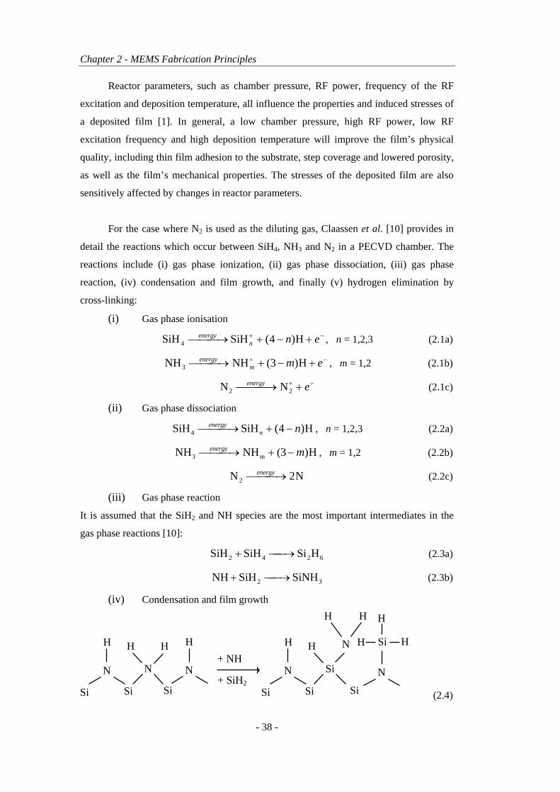
For the case where N2 is used as the diluting gas, Claassen et al. [10] provides in
detail the reactions which occur between SiH4, NH3 and N2 in a PECVD chamber. The
reactions include (i) gas phase ionization, (ii) gas phase dissociation, (iii) gas phase
reaction, (iv) condensation and film growth, and finally (v) hydrogen elimination by
cross-linking:
(i) Gas phase ionisation
−+ +−+⎯⎯ →⎯ ennenergy H)4(SiHSiH 4 , n = 1,2,3 (2.1a)
−+ +−+⎯⎯ →⎯ emmenergy H)3(NHNH3 , m = 1,2 (2.1b)
−+ +⎯⎯ →⎯ eenergy22 NN (2.1c)
(ii) Gas phase dissociation
H)4(SiHSiH4 nnenergy −+⎯⎯ →⎯ , n = 1,2,3 (2.2a)
H)3(NHNH m3 menergy −+⎯⎯ →⎯ , m = 1,2 (2.2b)
N2N2 ⎯⎯ →⎯energy (2.2c)
(iii) Gas phase reaction
It is assumed that the SiH2 and NH species are the most important intermediates in the
gas phase reactions [10]:
6242 HSiSiHSiH ⎯→⎯+ (2.3a)
32 SiNHSiHNH ⎯→⎯+ (2.3b)
(iv) Condensation and film growth
N NN
H H H H
Si Si Si
+ NH
+ SiH2N NSi
H H N Si
Si Si Si
H H
H
H
H
(2.4)
Chapter 2 - MEMS Fabrication Principles
- 39 -
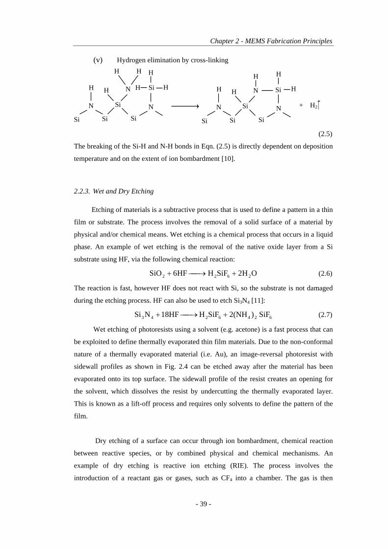
(v) Hydrogen elimination by cross-linking
N NSi
H H N Si
Si Si Si
H H
H
H
H
N NSi
H H N Si
Si Si Si
H H
H
+ H2
(2.5)
The breaking of the Si-H and N-H bonds in Eqn. (2.5) is directly dependent on deposition
temperature and on the extent of ion bombardment [10].
2.2.3. Wet and Dry Etching
Etching of materials is a subtractive process that is used to define a pattern in a thin
film or substrate. The process involves the removal of a solid surface of a material by
physical and/or chemical means. Wet etching is a chemical process that occurs in a liquid
phase. An example of wet etching is the removal of the native oxide layer from a Si
substrate using HF, via the following chemical reaction:
OH2SiFHHF6SiO 2622 +⎯→⎯+ (2.6)
The reaction is fast, however HF does not react with Si, so the substrate is not damaged
during the etching process. HF can also be used to etch Si3N4 [11]:
6246243 SiF )2(NHSiFH 18HFNSi +⎯→⎯+ (2.7)
Wet etching of photoresists using a solvent (e.g. acetone) is a fast process that can
be exploited to define thermally evaporated thin film materials. Due to the non-conformal
nature of a thermally evaporated material (i.e. Au), an image-reversal photoresist with
sidewall profiles as shown in Fig. 2.4 can be etched away after the material has been
evaporated onto its top surface. The sidewall profile of the resist creates an opening for
the solvent, which dissolves the resist by undercutting the thermally evaporated layer.
This is known as a lift-off process and requires only solvents to define the pattern of the
film.
Dry etching of a surface can occur through ion bombardment, chemical reaction
between reactive species, or by combined physical and chemical mechanisms. An
example of dry etching is reactive ion etching (RIE). The process involves the
introduction of a reactant gas or gases, such as CF4 into a chamber. The gas is then

Chapter 2 - MEMS Fabrication Principles
- 40 -
dissociated by energetic particles, i.e. plasma electrons. The radicals, such as CF3+, CF3
and F that are produced during the dissociation step migrate towards the substrate sample
surface, where they become adsorbed, diffuse over the surface and react with surface
species [1]. The reaction products are then desorbed and migrate back into the bulk gas.
The plasma can be either RF-generated and/or inductively coupled plasma (ICP)-
generated. ICP sources create high-density, low-pressure, low-energy plasma, which
increase the etch rate of the dry etch process. As dry etching utilises both physical and
chemical processes, a wet etch process tends to have a higher selectivity due to its
reliance on chemical reactions only. This is advantageous when trying to etch only a
single layer of material from a multilayered structure made from different materials.
2.3. Bulk Micromachining
Bulk micromachining is a special case of wet etching and involves the etching of
the substrate. Bulk micromachining is used to etch materials such as Si, SiC, GaAs, InP
and Ge [1]. With excellent machinability and low cost, single crystal Si is the most
common bulk micromachined material in industry and has been used to fabricate a range
of MEMS devices including pressure sensors and accelerometers [3, 12].
FIG. 2.4. Wet etching of photoresist in a lift-off process.

Chapter 2 - MEMS Fabrication Principles
- 41 -
The atoms in a Si crystal are arranged in a diamond lattice structure, with
tetrahedral atomic coordination, as shown in Fig. 2.5. The structure is face-centred cubic,
with four extra atoms inside the unit cell filling the tetrahedral positions [13]. The {111}
planes present the highest packing density. Consequently, these planes etch at the slowest
rate in an anisotropic etchant among all planes in the crystal structure [1]. Table 2.1
summarises three common etchants and their associated etch rate ratios relative to the
(100) and (111) planes for single crystal Si [14, 15]. A solution of hydrofluoric, nitric and
acetic acids (HNA) etch both the (100) and (111) planes at the same rate. This type of
etchants is known as an isotropic etchant. Tetramethyl-ammonium hydroxide (TMAH)
and KOH show drastic differences in etching rate between the two planes, and are
anisotropic. KOH exhibits extreme selectivity for (100) planes relative to (111), which is
a highly desirable property for certain fabrication processes. The actual etch rate of
crystal planes depend largely on agitation, concentration of the reactants and temperature
of the solution [14, 16, 17].
Si wafers are commonly oriented so that their planar faces are parallel to the (100),
(110) or (111) planes. Using an isotropic etchant however, it is irrelevant what the
orientation of the wafer is. Figure 2.6 (a) and (b) illustrate schematically cross-sectional
and isometric views, respectively of a (100)-oriented Si substrate etched anisotropically
in KOH solution. The top surface of the substrate is initially masked with a thin film
material and patterned either by wet or dry etching to expose the underlying silicon
FIG. 2.5. Unit cell of crystalline Si.

Chapter 2 - MEMS Fabrication Principles
- 42 -
surface. Due to the anisotropic nature of the etchant, the (111) planes are etched much
slower than the (100) and (110) planes, resulting in sloped surfaces at an angle 54.74°
from the horizontal. Upon further etching, these sloped surfaces will meet at either a
single point or line, depending on the shape of the mask. If the thin film mask is patterned
to expose the Si substrate in the shape of a square, the etched silicon will be in the shape
of a pyramid. In comparison, a rectangular mask opening will form V-grooves in the
substrate.
Figure 2.7 illustrates the process steps necessary to release a thin film
microcantilever from a (100)-oriented Si substrate using bulk micromachining
techniques. The film is first deposited uniformly across the top surface of the wafer
(Fig. 2.7(a)). The film is then patterned in the shape of microcantilevers (Fig. 2.7(b)).
After initial wet etching of the Si substrate in KOH solution, a break in the
crystallographic planes underneath the corners of the beam occurs. This results in further
etching of the Si substrate underneath the beam along its length, eventually working its
way to the beam’s base (Fig. 2.7(c)). A schematic illustration of a top view of a released
microcantilever is shown in Fig. 2.8 (a). For such a process to work successfully, the
sides of the beam must be oriented so that they lie along the <110> directions. However,
Table 2.1
Etch plane selectivity of common Si etchants.
Etchant (100)/(111) etch rate ratio HF, HNO3, CH3COOH (HNA) 1:1 TMAH up to 35:1 KOH up to 400:1
FIG. 2.6. Etching of (100)-oriented Si showing (a) cross-sectional view, and (b) isometric
view.

Chapter 2 - MEMS Fabrication Principles
- 43 -
this method will not work for fixed-fixed beams, as shown in Fig. 2.8(b). In this case, two
separate V-grooves will be etched into the substrate on either side of the beam, without
under cutting to release the beam. To release a fixed-fixed beam using (100)-oriented Si,
the structure must be aligned away from the <110> directions, as shown in Fig. 2.8(c). An
optical image of an actual released SiNxHy fixed-fixed beam using this method is shown
in Fig. 2.9.
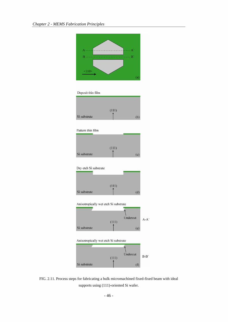
The supports of the fixed-fixed beam in Fig. 2.9 are obviously non-ideal. Fixed-
fixed beams with ideal supports can be successfully bulk micromachined using (111)-
oriented Si wafers [18]. Figure 2.10 shows an optical micrograph of an actual released
bulk micromachined SiNxHy fixed-fixed beam, deposited on an (111)-oriented Si wafer.
The steps required to fabricate a beam in this manner are shown in Fig. 2.11. The mask
FIG. 2.7. Schematic illustrations of the process steps used to release a microcantilever from
(100)-oriented Si using bulk micromachining techniques.

Chapter 2 - MEMS Fabrication Principles
- 44 -
layer is patterned in the shape of a hexagon, with a fixed-fixed beam suspended across its
centre. The sides of the hexagon represent <110> directions in the (111)-oriented Si wafer
[17]. The process involves a dry etch step of the Si-substrate to define the cavity size
underneath the beam. If this step is not carried out, long etch times will be necessary to
release the beam. As seen in Fig. 2.10, the Si substrate is in focus, which suggests the
cavity between the beam and the substrate is very small. In this case, the cavity size was
~2 µm.
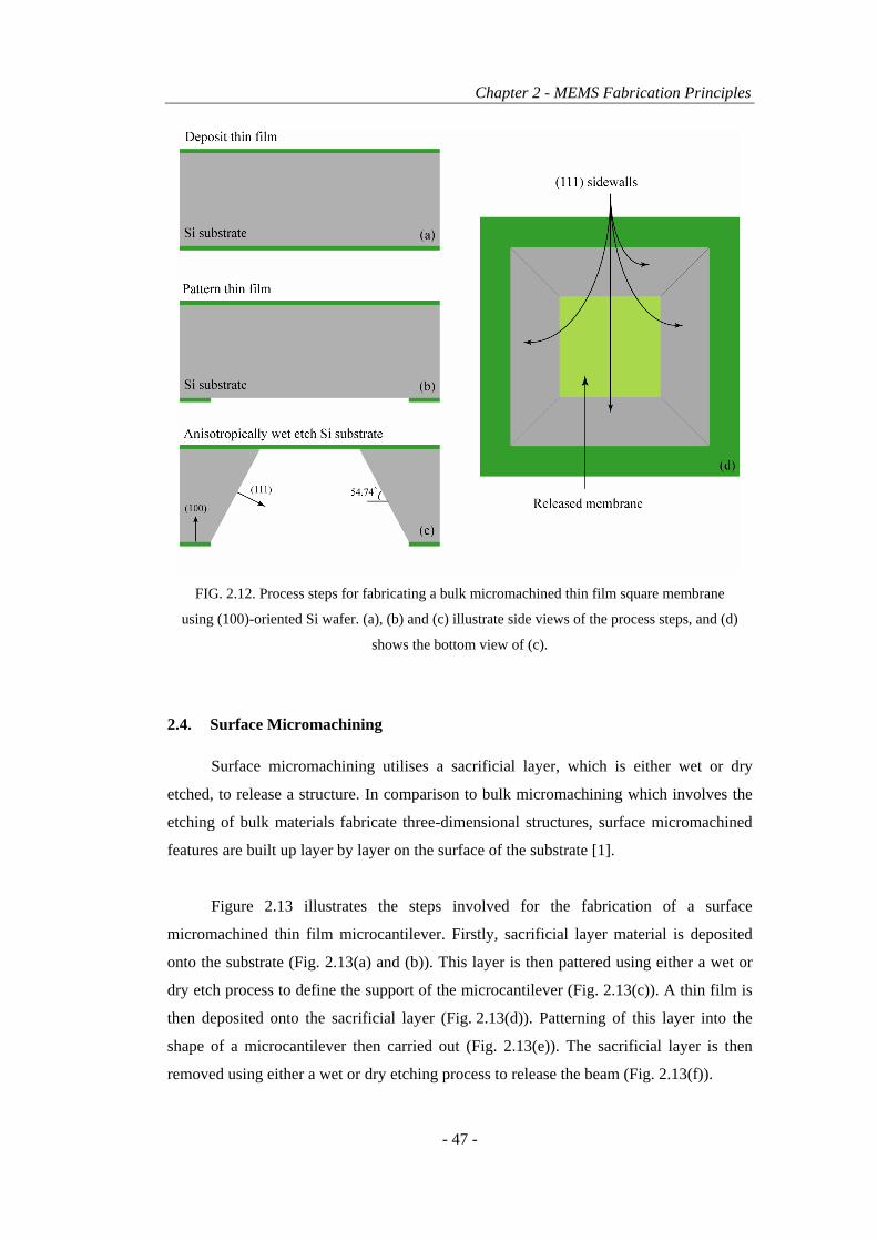
Circular, square and rectangular thin film membranes that are completely
constrained around their perimeter are common MEMS structures have been used to
sense changes in pressure [12]. MEMS-based pressure sensors are often fabricated using
bulk micromachining techniques. Circular-shaped membranes utilise an isotropic etchant
of the substrate, whilst square or rectangular-shaped membranes utilise an anisotropic
etchant. Figure 2.12 illustrates the steps required to fabricate a square membrane made of
thin film material using (100)-oriented single-crystal Si as the substrate and KOH as the
anisotropic etchant. Thin film material is initially deposited on both sides of the wafer
(Fig. 2.12(a)). Patterning of one of the films into the shape of a square is then carried out
(Fig. 2.12(b)), followed by an anisotropic etch of the substrate (Fig. 2.10(c)).
Figure 2.12(d) illustrates the bottom view of the released membrane. Due to the angle of
the (111) planes, the sides of the released membrane are smaller in dimension than the
etched pattern. The released membrane dimensions however can be easily calculated if
the thickness of the substrate is known.
FIG. 2.8. Schematic diagrams of the top views of, (a) a microcantilever released from a (100)-
oriented Si substrate, (b) fixed-fixed beam release failure (the beam is aligned to the <110>
direction), and (c) successful fixed-fixed beam release.

Chapter 2 - MEMS Fabrication Principles
- 45 -
30 µm
FIG. 2.9. Optical micrograph of a released SiNBx BH By B fixed-fixed beam. The beam was released by
etching the (100)-oriented Si substrate with KOH solution.
FIG. 2.10. Optical micrograph of a released SiN Bx BHBy B fixed-fixed beam. The beam was released
by etching the (111)-oriented Si substrate with KOH solution.
Chapter 2 - MEMS Fabrication Principles
- 46 -
FIG. 2.11. Process steps for fabricating a bulk micromachined fixed-fixed beam with ideal
supports using (111)-oriented Si wafer.
Chapter 2 - MEMS Fabrication Principles
- 47 -
2.4. Surface Micromachining
Surface micromachining utilises a sacrificial layer, which is either wet or dry
etched, to release a structure. In comparison to bulk micromachining which involves the
etching of bulk materials fabricate three-dimensional structures, surface micromachined
features are built up layer by layer on the surface of the substrate [1].
Figure 2.13 illustrates the steps involved for the fabrication of a surface
micromachined thin film microcantilever. Firstly, sacrificial layer material is deposited
onto the substrate (Fig. 2.13(a) and (b)). This layer is then pattered using either a wet or
dry etch process to define the support of the microcantilever (Fig. 2.13(c)). A thin film is
then deposited onto the sacrificial layer (Fig. 2.13(d)). Patterning of this layer into the
shape of a microcantilever then carried out (Fig. 2.13(e)). The sacrificial layer is then
removed using either a wet or dry etching process to release the beam (Fig. 2.13(f)).
FIG. 2.12. Process steps for fabricating a bulk micromachined thin film square membrane
using (100)-oriented Si wafer. (a), (b) and (c) illustrate side views of the process steps, and (d)
shows the bottom view of (c).

Chapter 2 - MEMS Fabrication Principles
- 48 -
FIG. 2.13. Process steps necessary for the fabrication of a surface micromachined
microcantilever.

Chapter 2 - MEMS Fabrication Principles
- 49 -
The choice of sacrificial layer material to use is dependent on the selectivity of its
removal process. Polyimide has previously been used as a sacrificial layer for defining
the cavity in surface micromachined FP filters [19]. This is because it can be easily
removed in a weak base solution at room temperature. The solution selectively etches
polyimide whilst having no affect on the other materials in the filter. Polyimide also has
the advantage of being a low-cost material that is easily spun onto a substrate, and can be
partially cured at relatively low temperatures (130 °C). This makes it compatible with
temperature sensitive substrates (e.g. Hg1-xCdxTe).
2.5. Fabrication Issues
2.5.1. Step Coverage
Step coverage is a major issue when fabricating MEMS structures using surface
micromachining techniques. PVD thin films are especially prone to poor step coverage
due to the highly directional nature of the deposition process. As illustrated in Fig. 2.14, if
the sample is positioned perpendicular to the direction of path of the evaporant, only the
horizontal surfaces will be coated with the evaporated material while vertical side walls
will receive little evaporated material
To improve the continuity of a PVD film, the side wall angle of the underlying thin
film needs to be altered. This can be achieved using a photoresist with an overcut profile,
which is used to define the pattern of the underlying thin film, followed by a dry etch. An
example of the procedure is shown in Fig. 2.15. In this case, the thin film underlying the
FIG. 2.14. Step-coverage of thermally evaporated Au.

Chapter 2 - MEMS Fabrication Principles
- 50 -
FIG. 2.15. Process steps necessary to improve step-coverage of PVD films.
Chapter 2 - MEMS Fabrication Principles
- 51 -
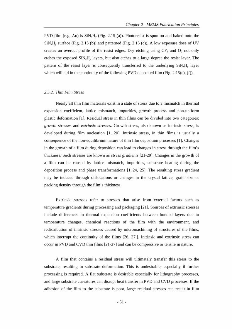
PVD film (e.g. Au) is SiNxHy (Fig. 2.15 (a)). Photoresist is spun on and baked onto the
SiNxHy surface (Fig. 2.15 (b)) and patterned (Fig. 2.15 (c)). A low exposure dose of UV
creates an overcut profile of the resist edges. Dry etching using CF4 and O2 not only
etches the exposed SiNxHy layers, but also etches to a large degree the resist layer. The
pattern of the resist layer is consequently transferred to the underlying SiNxHy layer
which will aid in the continuity of the following PVD deposited film (Fig. 2.15(e), (f)).
2.5.2. Thin Film Stress
Nearly all thin film materials exist in a state of stress due to a mismatch in thermal
expansion coefficient, lattice mismatch, impurities, growth process and non-uniform
plastic deformation [1]. Residual stress in thin films can be divided into two categories:
growth stresses and extrinsic stresses. Growth stress, also known as intrinsic stress, is
developed during film nucleation [1, 20]. Intrinsic stress, in thin films is usually a
consequence of the non-equilibrium nature of thin film deposition processes [1]. Changes
in the growth of a film during deposition can lead to changes in stress through the film’s
thickness. Such stresses are known as stress gradients [21-29]. Changes in the growth of
a film can be caused by lattice mismatch, impurities, substrate heating during the
deposition process and phase transformations [1, 24, 25]. The resulting stress gradient
may be induced through dislocations or changes in the crystal lattice, grain size or
packing density through the film’s thickness.
Extrinsic stresses refer to stresses that arise from external factors such as
temperature gradients during processing and packaging [21]. Sources of extrinsic stresses
include differences in thermal expansion coefficients between bonded layers due to
temperature changes, chemical reactions of the film with the environment, and
redistribution of intrinsic stresses caused by micromachining of structures of the films,
which interrupt the continuity of the films [26, 27,]. Intrinsic and extrinsic stress can
occur in PVD and CVD thin films [21-27] and can be compressive or tensile in nature.
A film that contains a residual stress will ultimately transfer this stress to the
substrate, resulting in substrate deformation. This is undesirable, especially if further
processing is required. A flat substrate is desirable especially for lithography processes,
and large substrate curvatures can disrupt heat transfer in PVD and CVD processes. If the
adhesion of the film to the substrate is poor, large residual stresses can result in film

Chapter 2 - MEMS Fabrication Principles
- 52 -
delamination [32-40]. In certain circumstances, a compressively stressed thin film can
delaminate from the substrate in the form of ‘telephone cord’ shaped patterns. An
example of this morphology is shown in Fig. 2.16 [40]. In this instance a 300 nm thick
tungsten film has delaminated from its substrate in regular, sinusoidal patterns in the
plane of the film. The buckled film adopts this morphology in order to balance the driving
force for delamination and the interfacial fracture energy [40]. In contrary to
compressively stressed films, large tensile stressed films can crack, which is also
undesirable [41-43].
Structures fabricated from thin films that contain residual stress can behave
differently to thin film structures containing zero stress. The difference in behaviour is
not only dependent on the type and magnitude of the stress it is also dependent on the
type of structure, as well as its dimensions and constraints. Figure 2.17 provides examples
of how stress can affect simply supported surface micromachined cantilever and fixed-
fixed beams. For the case of a microcantilever beam fabricated from a compressively
stressed film, such that the stress is homogenous through its thickness, the beam will
increase in length once the sacrificial layer is removed. This increase in length relaxes the
stress from the beam, resulting in a stress-free structure. The same effect will also occur
for a microcantilever beam that is fabricated from a homogenous tensile stressed film,
which will shorten its length once the sacrificial layer is removed. A microcantilever
FIG. 2.16. Optical micrograph of telephone cord buckles formed in 300 nm thick
Tungsten thin film [40].

Chapter 2 - MEMS Fabrication Principles
- 53 -
beam that is fabricated from a film with a non-homogenous stress through its thickness
(i.e. a stress gradient) will bow either up or down once the sacrificial layer is removed. In
this particular example, the top surface of the microcantilever is more tensile (or less
compressive) than the bottom surface, resulting in the beam curving upwards. The
opposite curvature will form if the sign of the stress gradient is reversed.
A fixed-fixed beam (Fig. 2.17(b)) that is fabricated from a homogenous
compressively stressed thin film will buckle, provided that the compressive stress is
greater than the Euler buckling limit, which is also a function of the Young’s modulus of
the film and beam geometry [12]. The shape of the bulking profile is dependent on the
type of constraints of the beam, as well as the beam’s dimensions [44]. Thin film fixed-
fixed beams generally only experience first-order buckling profiles, however higher order
profiles are possible if the long beams are fabricated [44]. For a fixed-fixed beam
FIG. 2.17. Comparison of the affects of compressive and tensile stress, and stress gradient on
microcantilever beams (a) and fixed-fixed beams (b).

Chapter 2 - MEMS Fabrication Principles
- 54 -
fabricated from a homogenous tensile stressed film, its shape will not change after the
removal of the sacrificial layer. Consequently, the stress in the original film is conserved
in the beam so long as the stress in the beam is less than its failure strength. Fixed-fixed
beams that experience a stress gradient will maintain their original state after release
provided the net stress in the beam is tensile, or less than Euler buckling limit if it is
compressive.
Circular, square and rectangular membranes that are constrained around their
perimeter behave similarly to fixed-fixed beams when subjected to residual stress. As
their dimensions and boundary conditions are different compared to fixed-fixed beams, it
is expected the amount of stress required fail or buckle a membrane will be different. Due
to their higher constraints, membranes can achieve higher orders of buckling compared to
fixed-fixed beams. Figure 2.18 illustrates buckled PECVD silicon nitride thin film square
membranes of varying lateral dimensions [45]. It is obvious that the magnitude of
buckling the membrane experiences is dependent on its dimensions.
FIG. 2.18. Optical micrographs of square PECVD silicon nitride membranes with lateral
dimensions (a) 601 µm, (b) 1014 µm, (c) 1425 µm, and (d) 1980 µm [45].

Chapter 2 - MEMS Fabrication Principles
- 55 -
2.5.3. Stiction
Utilising a wet etch process to remove a sacrificial layer can be advantageous with
regards to selectivity, cost and time. However, once the sample is wet released, it will
need to be dried. Drying of MEMS structures and devices is not a trivial process,
especially for surface micromachined structures where distances between suspended
structures and the underlying substrate can be less than a few microns. A drying process
that removes unwanted liquid from a sample by evaporation will cause any liquid trapped
underneath a suspended structure to decrease in volume. The forces due to surface tension
will pull the suspended structure towards the substrate. Once the structure comes into
contact with the substrate, van der Waals’ dispersion forces between the two bodies will
bond the two surfaces together. If these forces are greater than the restoring force of the
suspended structure, the structure will be permanently bonded to the substrate. This is
known as stiction, and can severely limit device yield and greatly increase fabrication
costs [3].
Stiction is a common problem when drying surface micromachined structures.
Critical point drying (CPD) is a common and successful procedure which helps to avoid
stiction under these circumstances [3]. In this procedure, samples are initially dehydrated
in a fluid that is miscible with liquid CO2 (e.g. methanol). Samples are loaded into a CPD
chamber (still submerged in the dehydrating fluid), which is then sealed. The fluid is then
displaced with liquid CO2 at room temperature and 10 atms pressure. The chamber is then
heated, and due to the fixed volume of the chamber, the pressure also increases. The
process is designed to increase the pressure and temperature of the liquid CO2 past its
critical point (31.1 °C, 73 atm) and in doing so the phase transition from liquid CO2 to
gaseous CO2 is avoided. The chamber, once filled with this supercritical gas, is slowly
released from its pressure back to room pressure, whilst maintaining the elevated
temperature. The result is a dried sample with structures feely suspended above the
substrate.
2.6. Summary
This chapter has reviewed the techniques and principles for the synthesis of thin
film materials and fabrication of MEMS structures using thin film materials. The methods
discussed have been utilised in this study to fabricate structures for the determination of

Chapter 2 - MEMS Fabrication Principles
- 56 -
material properties of thin film materials, as well as for the fabrication of FP filters.
Details on this work can be found in Chapters four and five of this thesis, respectively.
References
1. M. J. Madou, Fundamentals of Microfabrication: The Science of Miniaturization 2nd ed., CRC, Boca Raton (2002).
2. M. Furuta, S. Asaumi and A. Yokota, “Mechanism of dissolution inhibition of
novolak-diazoquinone resist,” Proceedings of the SPIE, 1466, p. 477-484. 3. K. J. Winchester, Tunable Microelectromechanical Fabry-Perot Filters Using
Plasma Enhanced Chemical Vapour Deposited Silicon Nitride Membranes, PhD Thesis, University of Western Australia (2003).
4. O. Tabata, K. Kawahata, S. Sugiyama, and I. Igarashi, “Mechanical property
measurement of thin films using load-deflection of composite rectangular membranes,” Sensors and Actuators A, 20, p. 135-141 (1989).
5. C. H. Mastrangelo, Y-C Tai, and R. S. Muller, “Thermophysical properties of low-
residual stress, silicon-rich, LPCVD silicon nitride films,” Sensors and Actuators A, 23, p. 856-880 (1990).
6. T. Hasegawa, T. Date, A. Karen, and A. Masuda, “Study on change in SIMS
intensities near the interface between silicon-nitride film and silicon substrate,” Applied Surface Science, 231-232, p. 725-728 (2004).
7. D. L. Smith, A. S. Alimonda, C-C Chen, S. E. Ready, and B. Wacker, “Mechanism
of SiNxHy deposition from NH3-SiH4 plasma,” Journal of the Electrochemical Society, 137, p. 614-623 (1990).
8. M. T. K. Soh, N. Savvides, C. A. Musca, M. P. Martyniuk, and L. Faraone, “Local
bonding environment of plasma deposited nitrogen-rich silicon nitride thin films,” Journal of Applied Physics, 97, p. 93714-1-8, (2005).
9. A. Okhrimovskyy, A. Bogaerts and R. Gijbels, “Incorporating the gas flow in a
numerical model of rf discharges in methane,” Journal of Applied Physics, 96, p. 3070-3076, (2004).
10. W. A. P. Claassen, W. G. J. N. Valkenburg, M. F. C. Willemsen and W. M. van de
Wijgert, “Influence of deposition temperature, gas pressure, gas phase composition, and RF frequency on composition and mechanical stress of plasma silicon nitride layers,” Journal of the Electrochemical Society, 132, p. 893-899 (1985).
11. K. B. Sundaram, R. E. Sah, H. Baumann, K. Balachandran and R. M. Todi, “Wet
etching studies of silicon nitride thin films deposited by electron cyclotron resonance (ECR) plasma enhanced chemical vapor deposition,” Microelectronic Engineering, 70, p. 109-114 (2003).
12. S. D. Senturia, Microsystem Design, Kluwer Academic Publishers, Boston (2001).

Chapter 2 - MEMS Fabrication Principles
- 57 -
13. W. D. Callister, Materials Science and Engineering: An Introduction 5th ed., John
Wiley & Sons, Inc., New York (2000). 14. K. E. Petersen, “Silicon as a mechanical material,” Proceedings of the IEEE, 70, p.
420-457 (1982). 15. P. J. French and P. M. Sarro, “Surface versus bulk micromachining – the contest for
suitable applications,” Journal of Micromechanics and Microengineering, 8, p. 45-53 (1998).
16. H. Seidel, L. Csepregi, A. Heuberger and H. Baumgärtel, “Anisotropic etching of
crystalline silicon in alkaline solutions,” Journal of the Electrochemical Society, 137, p. 3612-3626 (1990).
17. E. Steinsland, T. Finstad and A. Hanneborg, “Etch rates of 100 , 111 and 110
single-crystal silicon in TMAH measured in situ by laser reflectance interferometry,” Sensors and Actuators A, 86, p. 73-80 (2000).
18. H. Hu, H. Lin, W. Fang and B.C.S.Chou, “The diagnostic micromachined beams on
(111) substrate,” Sensors and Actuators A, 93, p. 258-265 (2001). 19. J. M. Dell, C. A. Musca, J. Antoszewski and L. Faraone, “Tunable Infrared Sensors
– Integration of MEMS with Semiconductor Detectors,” IEEE/LEOS International Conference on Optical MEMS and Their Applications, p. 5-6 (2006).
20. L. B. Freund and S. Suresh, Thin Film Materials, Cambridge University Press, UK
(2003). 21. Y. Pauleau, “Generation and evolution of residual stresses in physical vapour-
deposited thin films,” Vacuum, 61, p 175-181 (2001). 22. J. Singh, S. Chandra and A. Chand, “Strain studies in LPCVD polysilicon for
surface micromachined devices,” Sensors and Actuators A, 77, p. 133–138 (1999). 23. S. G. Mayr and K. Samwer, “Model for intrinsic stress formation in amorphous thin
films,” Physical Review Letters, 87, p. 036105-1-4 (2001). 24. S. Shao, Z. Fan, J. Shao, H. He, “Evolutions of residual stress and microstructure in
ZrO2 thin films deposited at different temperatures and rates,” Thin Solid Films, 445, p. 59-62 (2003).
25. G. Guisbiers, S. Strehle and M. Wautelet, “Modeling of residual stresses in thin
films deposited by electron beam evaporation,” Microelectronic Engineering, 82, p. 665-669 (2005).
26. M. Martyniuk, Low-Temperature Micro-Opto-Electro-Mechanical Technologies for
Temperature Sensitive Substrates, PhD Thesis, University of Western Australia (2006).
27. W-S Liao, C-H Lin and S-C Lee, “Oxidation of silicon nitride prepared by plasma-
enhanced chemical vapor deposition at low temperature,” Applied Physics Letters, 65, p. 2229-2231 (1994).

Chapter 2 - MEMS Fabrication Principles
- 58 -
28. J. P. Harbison, A. J. Williams and D. V. Lang, “Effect od silane dilution on intrinsic
stress in glow discharge hydrogenated amorphous silicon films,” Journal of Applied Physics, 55, p. 946-951 (1984).
29. C. L. G. Alzar, “Mechanical stress reduction in PECVD a-Si:H thin films,”
Materials Science and Engineering B, 65, p. 123-126 (1999). 30. J. Yota, J. Hander and A. A. Saleh, “A comparative study on inductively-coupled
plasma high-density plasma, plasma-enhanced, and low pressure chemical vapor deposition silicon nitride films,” Journal of Vacuum Science & Technology A, 18, p. 372-376 (2000).
31. D. Resnik, U. Aljancic, D. Vrtacnik, M. Mozek and S. Amon, “Mechanical stress
in thin film microstructures on silicon substrate,” Vacuum, 80, p 236-240 (2005). 32. W. Anwen, “Axisymmetric and asymmetric postbuckling response and energy
release rate of delaminated circular film,” International Journal of Mechanical Sciences, 41, p. 43-58 (1999).
33. L. U. J. T. Ogbuji and D. R. Harding, “A novel method for determining the strength
of PECVD silicon (oxy)nitride films,” Thin Solid Films, 263, p. 194-197 (1995). 34. H. M. Jensen and M. D. Thouless, “Effects of residual stress in the blister test,”
International Journal of Solid Structures, 30, p. 779-795 (1993). 35. J. K. Pierson and J. Roorda, “Delamination buckling in circular plates,” Thin-
Walled Structures, 18, p. 161-175 (1994). 36. M. W. Moon, H. M. Jensen, J. W. Hutchinson, K. W. Oh and A. G. Evans, “The
characterization of telephone cord buckling of compressed thin films on substrates,” Journal of the Mechanics and Physics of Solids, 50, p. 2355-2377 (2002).
37. G. Gioia and M. Ortiz, “Determination of thin-film debonding parameters from
telephone-cord measurements,” Acta Materialia, 46, p. 169-175 (1998). 38. P. Goudeau, Philippe P. Villain, N. Tamura, H. A. Padmore, “Mesoscale x-ray
diffraction measurement of stress relaxation associated with buckling in compressed thin films,” Applied Physics Letters, 83, p. 51-53 (2003).
39. A. Lee, B. M. Clemens, W. D. Nix, “Stress induced delamination methods for the
study of adhesion of Pt thin films to Si,” Acta Materialia, 52, p. 2081-2093 (2004). 40. M. J. Cordill, D. F. Bahr, N. R. Moody and W. W. Gerberich, “Adhesion
measurements using telephone cord buckles,” Materials Science and Engineering A, 443, p. 150-155 (2007).
41. P. Wellner, O. Kraft, G. Dehm, J. Andersons and E. Arzt, “Channel cracking of β-
NiAl thin films on Si substrates,” Acta Materialia, 52, p. 2325-2336 (2004). 42. Z. C. Xia and J. W. Hutchinson, “Crack patterns in thin films,” Journal of the
Mechanics and Physics of Solids, 48, p. 1107-1131 (2000).

Chapter 2 - MEMS Fabrication Principles
- 59 -
43. M. George, C. Coupeau, J. Colin and J. Grilhe, “Mechanical behaviour of metallic thin films on polymeric substrates and the effect of ion beam assistance on crack propagation,” Acta Materialia, 53, p. 411-417 (2005).
44. W. Fang and J. A. Wickert, “Post-buckling of micromachined beams,” Proceedings
IEEE Micro Electro Mechanical Systems, p. 182-187 (1994). 45. V. Ziebart and O. Paul, “Strongly buckled square micromachined membranes,”
Journal of Microelectromechanical Systems, 8, p. 423-432 (1999).

Chapter 3 - Thin Film Mechanics and Actuation Methods
- 60 -
Chapter 3
Thin Film Mechanics and Actuation
Methods
As essentially mechanical structures, thin-film components of MEMS devices are
designed to experience mechanical forces. For example, the FP filter illustrated in Fig. 1.7
utilises electrostatics to provide a distributed load over an electrode’s surface, which
results in movement of the top mirror towards the bottom mirror. In order to understand
how a thin film structure behaves under load requires the knowledge of basic solid
mechanics and actuation principles. This chapter outlines the mechanics of thin films
deposited on substrates, thin-film microcantilever beams, fixed-fixed beams and
membranes under various loads, such as point loads, distributed loads, and internal
stresses. Common MEMS actuation principles are also presented with particular emphasis
to those that are relevant to this work. Finally, the vibration behaviour of thin film
structures subjected to different environments is also discussed. The structures described
in this chapter are those directly related to determining the properties of thin films
presented in Chapter 4 and FP filter designs presented in Chapter 5 of this thesis.
3.1. Mechanics of Materials
As a brief introduction to mechanics, the elastic prismatic bar of initial length (L)
and cross sectional area (A) is presented in Fig. 3.1. When a force (F) is applied axially to
the bar, it will elongate to L1 in the direction of the force. The axial stress (σa)
experienced by the bar due to F can be described as:
AF
a =σ (3.1)
The axial strain (εa) experienced by the bar can be described using:
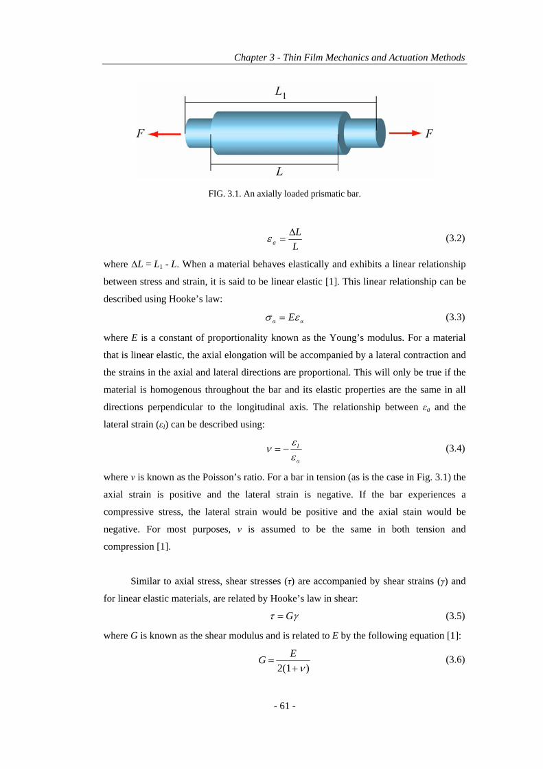
Chapter 3 - Thin Film Mechanics and Actuation Methods
- 61 -
LL
a∆
=ε (3.2)
where ∆L = L1 - L. When a material behaves elastically and exhibits a linear relationship
between stress and strain, it is said to be linear elastic [1]. This linear relationship can be
described using Hooke’s law:
αα Eεσ = (3.3)
where E is a constant of proportionality known as the Young’s modulus. For a material
that is linear elastic, the axial elongation will be accompanied by a lateral contraction and
the strains in the axial and lateral directions are proportional. This will only be true if the
material is homogenous throughout the bar and its elastic properties are the same in all
directions perpendicular to the longitudinal axis. The relationship between εa and the
lateral strain (εl) can be described using:
α
l
εεν −= (3.4)
where ν is known as the Poisson’s ratio. For a bar in tension (as is the case in Fig. 3.1) the
axial strain is positive and the lateral strain is negative. If the bar experiences a
compressive stress, the lateral strain would be positive and the axial stain would be
negative. For most purposes, ν is assumed to be the same in both tension and
compression [1].
Similar to axial stress, shear stresses (τ) are accompanied by shear strains (γ) and
for linear elastic materials, are related by Hooke’s law in shear:
γτ G= (3.5)
where G is known as the shear modulus and is related to E by the following equation [1]:
)2(1 ν+
=EG (3.6)
FIG. 3.1. An axially loaded prismatic bar.

Chapter 3 - Thin Film Mechanics and Actuation Methods
- 62 -
Equation (3.6) shows that E, G and ν are not independent elastic properties of a material.
These properties describe how a material will deform when subjected to external and
internal forces, so long as the forces do not induce permanent deformation or fracture of
the material. Generally, structures are designed to function in the linear elastic region.
3.2. Plane Stress and Plane Strain
MEMS structures and devices are usually fabricated from thin-film materials with
thicknesses that can be orders of magnitude smaller in dimension compared to the length
and width of the structure. In these circumstances, plane stress and plane strain behaviour
can exist and are affected by boundary conditions. For example, the internal stress in an
isotropic thin film deposited onto a substrate can be described as biaxial. Biaxial stress is
a special condition of plane stress which is depicted using the element shown in
Fig. 3.2(a). The element has dimensions a, b and c, in the x, y, and z-directions,
respectively and is subjected to a plane stress condition where it only experiences normal
stresses in two of the three directions, i.e. σx and σy, and a shear stress τxy. The normal
strains εx, εy and εz can be expressed in terms of stresses σx and σy by superimposing the
effects of the individual stresses [1]:
)(1yxx E
νσσε −= (3.7)
)(1xyy E
νσσε −= (3.8)
)( yxz Eσσνε +−= (3.9)
For the biaxial stress condition of the thin film shown in Fig. 3.2(b), τxy = 0 and σx = σy
and consequently Eqns. (3.7), (3.8) and (3.9) simplify to:
yx
x Eεν
σε =−= )1( (3.10)
E
xz
νσε
2−= (3.11)
Rearrangement of Eqn. (3.10) yields:
xxE εν
σ)1( −
= (3.12)
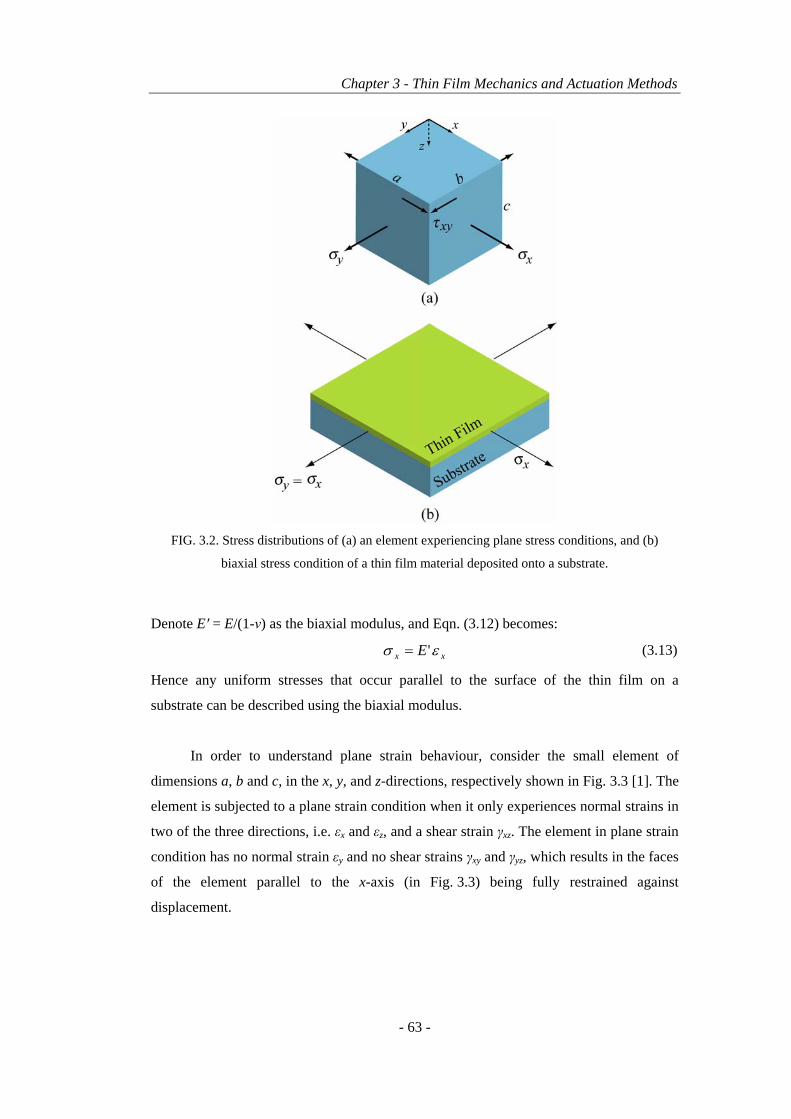
Chapter 3 - Thin Film Mechanics and Actuation Methods
- 63 -
Denote E′ = E/(1-ν) as the biaxial modulus, and Eqn. (3.12) becomes:
xx E εσ '= (3.13)
Hence any uniform stresses that occur parallel to the surface of the thin film on a
substrate can be described using the biaxial modulus.
In order to understand plane strain behaviour, consider the small element of
dimensions a, b and c, in the x, y, and z-directions, respectively shown in Fig. 3.3 [1]. The
element is subjected to a plane strain condition when it only experiences normal strains in
two of the three directions, i.e. εx and εz, and a shear strain γxz. The element in plane strain
condition has no normal strain εy and no shear strains γxy and γyz, which results in the faces
of the element parallel to the x-axis (in Fig. 3.3) being fully restrained against
displacement.
FIG. 3.2. Stress distributions of (a) an element experiencing plane stress conditions, and (b)
biaxial stress condition of a thin film material deposited onto a substrate.
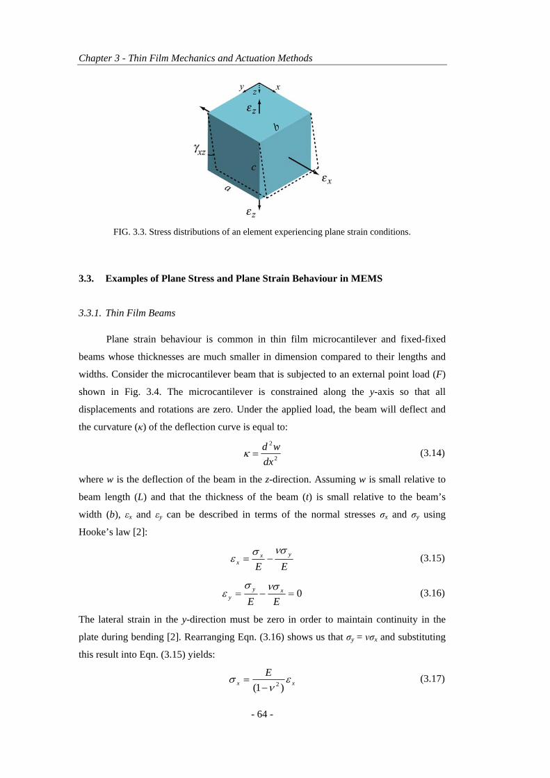
Chapter 3 - Thin Film Mechanics and Actuation Methods
- 64 -
3.3. Examples of Plane Stress and Plane Strain Behaviour in MEMS
3.3.1. Thin Film Beams
Plane strain behaviour is common in thin film microcantilever and fixed-fixed
beams whose thicknesses are much smaller in dimension compared to their lengths and
widths. Consider the microcantilever beam that is subjected to an external point load (F)
shown in Fig. 3.4. The microcantilever is constrained along the y-axis so that all
displacements and rotations are zero. Under the applied load, the beam will deflect and
the curvature (κ) of the deflection curve is equal to:
2
2
dxwd
=κ (3.14)
where w is the deflection of the beam in the z-direction. Assuming w is small relative to
beam length (L) and that the thickness of the beam (t) is small relative to the beam’s
width (b), εx and εy can be described in terms of the normal stresses σx and σy using
Hooke’s law [2]:
EE
yxx
νσσε −= (3.15)
0=−=EE
xyy
νσσε (3.16)
The lateral strain in the y-direction must be zero in order to maintain continuity in the
plate during bending [2]. Rearranging Eqn. (3.16) shows us that σy = νσx and substituting
this result into Eqn. (3.15) yields:
xxE εν
σ)1( 2−
= (3.17)
FIG. 3.3. Stress distributions of an element experiencing plane strain conditions.

Chapter 3 - Thin Film Mechanics and Actuation Methods
- 65 -
Denote E* = E/(1-ν2) as the plate modulus, and Eqn. (3.17) becomes:
xx E εσ *= (3.18)
Hence the stress distribution in a beam that experiences plane strain conditions can be
described using the plate modulus, and is applicable for beams which are designed so that
b≥5t [2, 3].
For a beam that undergoes a deflection due to an external force (such as the beam
illustrated in Fig. 3.4), an element of area dA at distance z from the neutral axis will
undergo elongation εx equal to:
zx κε −= (3.19)
Substituting Eqn. (3.19) into Eqn. (3.18) yields:
zEx κσ *−= (3.20)
The normal stress σx acting on the element dA in Fig. 3.4 produces an element of moment
(dM) equal to -σxzdA. The integral of all such elemental moments over the entire cross-
sectional area (A) must equal the bending moment:
IEdAzEdAzMAA
x κκσ *2* ==−= ∫∫ (3.21)
where:
dAzIA∫= 2 (3.22)
is the moment of inertia of the beam. For a beam of rectangular cross-section profile, I is
expressed as [1]:
FIG. 3.4. Bending of a microcantilever beam.

Chapter 3 - Thin Film Mechanics and Actuation Methods
- 66 -
12
3btI = (3.23)
Substituting Eqn. (3.14) into Eqn. (3.21) yields:
IE
Mdx
wd*2
2
= (3.24)
This equation can be integrated to find the deflection at any point along the length of the
beam. For the microcantilever shown in Fig. 3.4, it can be shown that the deflection at the
end of the beam is equal to [1]:
3
3 *
FLwE I
= (3.25)
In certain situations, the thickness of a microcantilever beam fabricated using bulk
micromachining processes will be tapered. As discussed in Chapter 2, the release of a
microcantilever on (100)-oriented Si in KOH solution occurs across the length of the
beam as the substrate is removed. If some etching of the beam occurs during this process,
the beam’s cross section will look similar to that shown in Fig. 3.5 below:
For the case where a microcantilever beam’s thickness decreases linearly along its
length towards the tip, i.e. its thickness at its base is greater than at its end, Eqns. (3.23)
and (3.25) require further development as the beam’s bending moment varies along its
length. By integrating the bending moment of a cantilever beam of varying thickness, the
beam’s deflection (w) when subjected to a point load F can be calculated using:
* 3 2
(3 2 )6 2 ln(1 )( )
t
t t
mL mL tF mLwE bm t t mL
⎛ ⎞+⎛ ⎞⎛ ⎞= + −⎜ ⎟⎜ ⎟⎜ ⎟ +⎝ ⎠⎝ ⎠⎝ ⎠ (3.26)
FIG. 3.5. Tapered microcantilever beam due to bulk micromachining processes.

Chapter 3 - Thin Film Mechanics and Actuation Methods
- 67 -
where tt is the thickness of the beam at the point where the load F is applied and m is the
gradient of the beam thickness. The derivation of Eqn. (3.26) is shown in Appendix A of
this thesis.
3.3.2. Thin Film Membranes
In addition to slender beam structures, membranes are another common form of
mechanical structures in MEMS devices. Thin film membrane structures are commonly
subjected to distributed loads, such as pressure loads or electrostatic loads. Piezoresistive
pressure sensors are typical examples of MEMS devices that utilise thin film square or
rectangular membranes. These membranes are released from their substrate, but are still
constrained around their perimeter. A pressure difference across the membrane results in
bulging of the membrane. Piezoresistive sensors deposited on one side of the membrane
allow for accurate measurement of the induced bending strain, which can then be
correlated to the pressure difference [4]. For a square thin-film membrane with zero
residual stress that is constrained around the perimeter, the bulge height at the central
point of the square is related to the applied pressure by [2, 5-7]:
3
4
( ) s
s
f E'twPa
ν= (3.27)
where P is the uniform applied pressure on the membrane, t is the membrane thickness,
ws is the bulge height at the centre, as is the half length of the side of the square, and f(ν)
is a function of Poisson’s ratio, which is material-independent [5]. Table 3.1 summarizes
recently reported expressions for f(ν) for square membranes [8].
One would assume the inclusion of E′ is a result of the square membrane
experiencing biaxial stress conditions. However, the inclusion of f(ν) suggests that this is
not entirely true [5]. The strain experienced by the membrane varies from biaxial in the
centre of the membrane to plane strain at the edges and consequently E′ is insufficient to
characterise the behaviour of the membrane under an applied pressure.
Table 3.1 f(ν) expression for square thin-film membranes.
Authors f(ν)
Pan et al. (1990) [6] 1.37(1.446 - 0.427 ν) Vlassak and Nix (1992) [5] (0.800 + 0.062 ν)-3
Maier-Schneider et al. (1995) [7] 1.994(1 - 0.271 ν)

Chapter 3 - Thin Film Mechanics and Actuation Methods
- 68 -
For a rectangular membrane with a sufficiently large length-to-width aspect ratio
that is constrained around the perimeter, the bulge deformation of the membrane under
uniform applied pressure conforms to the plane strain condition, and the bulge contours
are parallel to the long sides of the rectangle, except at the ends. For a rectangular
membrane of side dimensions 2ar by 2br, the plane strain condition has been empirically
determined to be met when br ≥ 4ar [5]. Structures that meet this condition are referred to
as infinite rectangles in this discussion. Under the plane strain condition, the central line
bulge height (wr) and uniform applied pressure relationship is expressed as [5]:
3
4
43
*r
r
E twPa
= (3.28)
Equations (3.27) and (3.28) have been derived using an energy minimisation
method, under the condition that the total elastic strain energy of the system is at a
minimum with respect to the unknown parameters of the displacement field [5]. The
potential energy of a membrane under a uniform applied pressure is represented by the
strain energy of the membrane due to stretching, as well as the potential energy of the
pressure applied to the membrane. Equations (3.27) and (3.28) do not include the effects
of bending as part of the total strain energy of the membrane, which is a valid
approximation when the membrane thickness is much less than the membrane side
dimensions. Consequently, membranes are usually designed so that the as/t and ar/t ratios
are greater than 1000 [5, 6, 9-11].
3.4. Effects of Stress on Thin Film Structures
3.4.1. Microcantilever Beams
In Chapter 2 it was shown that a microcantilever beam fabricated from a thin film
material with in-plane homogenous residual stress (σ0) will change its length when
released from its substrate. The result is a stress-free microcantilever beam that is planar
and parallel to the substrate. The removal of stress during the release process will also
occur for microcantilever beams fabricated from thin film materials that exhibit a stress
gradient (δσ/δt) through the thickness. In this case however, the beam will bow with a
radius of curvature (R) depending on the sign of δσ/δt. The stress gradient may be
determined from the strain gradient (δε/δt) of the film using [12, 13]:
Ett δ
δεδδσ
= (3.29)
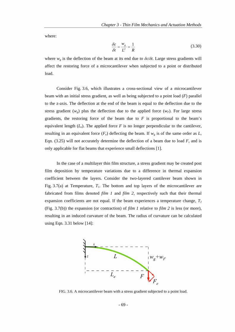
Chapter 3 - Thin Film Mechanics and Actuation Methods
- 69 -
where:
RL
wt
g 12 ==
δδε (3.30)
where wg is the deflection of the beam at its end due to δε/δt. Large stress gradients will
affect the restoring force of a microcantilever when subjected to a point or distributed
load.
Consider Fig. 3.6, which illustrates a cross-sectional view of a microcantilever
beam with an initial stress gradient, as well as being subjected to a point load (F) parallel
to the z-axis. The deflection at the end of the beam is equal to the deflection due to the
stress gradient (wg) plus the deflection due to the applied force (wF). For large stress
gradients, the restoring force of the beam due to F is proportional to the beam’s
equivalent length (Le). The applied force F is no longer perpendicular to the cantilever,
resulting in an equivalent force (Fe) deflecting the beam. If wg is of the same order as L,
Eqn. (3.25) will not accurately determine the deflection of a beam due to load F, and is
only applicable for flat beams that experience small deflections [1].
In the case of a multilayer thin film structure, a stress gradient may be created post
film deposition by temperature variations due to a difference in thermal expansion
coefficient between the layers. Consider the two-layered cantilever beam shown in
Fig. 3.7(a) at Temperature, T1. The bottom and top layers of the microcantilever are
fabricated from films denoted film 1 and film 2, respectively such that their thermal
expansion coefficients are not equal. If the beam experiences a temperature change, T2
(Fig. 3.7(b)) the expansion (or contraction) of film 1 relative to film 2 is less (or more),
resulting in an induced curvature of the beam. The radius of curvature can be calculated
using Eqn. 3.31 below [14]:
FIG. 3.6. A microcantilever beam with a stress gradient subjected to a point load.

Chapter 3 - Thin Film Mechanics and Actuation Methods
- 70 -
2121212112
22
222
21
211
2221
21212121
))((6)()()232(2
bbttEEttbtEbtEttttbbttEER
+−++++
=εε
(3.31)
where E1, t1, b1 and ε1 represent the Young’s modulus, thickness, width and strain of
film 1, respectively, and E2, t2, b2 and ε2 represent the Young’s modulus, thickness, width
and strain of film 2, respectively. Induced stress gradients due to thermal expansion
mismatch of bi-layers is common when thin films are deposited at higher temperatures
than the operating temperature of the structure. At the deposition temperature, the two
films may be formed in harmony (i.e. zero stress gradient), however when cooled down to
the ambient temperature, stresses are generated due to the thermal expansion mismatch.
In order to remove induced stress gradient variations due to temperature variations, thin
film structures can be designed with three layers instead of two. The tri-layer
microcantilever beam shown in Fig. 3.7(c) consists of film 1, film 2 and film 1 alternate
layers. This structure will remain flat even if the temperature is varied to from T1 to T2
(Fig. 3.7(d)) as the induced bending moment created between the bottom and centre
layers (due to differences in thermal expansion coefficient) cancels out the induced
bending moment created between the centre and top layers. However the net bending
moment will only equal zero if the thickness of the top and bottom films are the same.
3.4.2. Fixed-Fixed Beams
For a fixed-fixed beam constrained so that all displacements and rotations are zero
at both ends, a point load F applied at the centre of the beam will result in a displacement,
as shown in Fig, 3.8. The load can be approximated by [4, 12]:
FIG. 3.8. A fixed-fixed beam subjected to a point load in the centre.
FIG. 3.7. Multilayer microcantilevers showing, (a) bi-layer before release, (b) bi-layer after
release, (d) tri-layer before release, and (d) tri-layer after release.

Chapter 3 - Thin Film Mechanics and Actuation Methods
- 71 -
33
4*20
34*
826w
LtbEw
Ltbw
LtbEF ⎟
⎠⎞
⎜⎝⎛+⎟
⎠⎞
⎜⎝⎛+⎟
⎠⎞
⎜⎝⎛=
ππσπ (3.32)
where w is the central beam deflection, and σ0 is the residual stress in the beam. The first,
second and third terms in Eqn. (3.32) represent the beam’s resorting force due to its
bending, residual stress and stretching components, respectively. At small deflections, the
restoring force is dominated by bending and residual stress components, while at large
deflections it is dominated by the stretching of the beam. Equation (3.32) is only an
approximation of the exact solution which can be determined using computational
simulations [4], however it has been shown it is accurate to within 1.5% for small
deflections [12, 15].
If a fixed-fixed beam undergoes enough compressive stress that it exceeds the
Euler buckling limit, it will buckle [4]. The compressive strain (ε0) experienced by the
buckled beam is equal to the Euler strain (εEuler) plus the axial strain (εa) [4, 12]:
⎟⎟⎠
⎞⎜⎜⎝
⎛+−=+=
34
22
2
2
0tw
LEuleraπεεε (3.33)
where w is the deflection of the beam at the centre. The residual stress (σ0) can be
calculated using σ0 = ε0E*.
3.4.3. Thin Film Membranes
For the case where a membrane contains a tensile residual stress σ0, the
relationship between the applied pressure (P) and the central point bulge height (ws) of a
square membrane is given by [5-7]:
302 4
( ) 's s s
s s
t f E tP c w wa aσ ν
= + (3.34)
where cs is a geometry-dependent constant equal to 3.393 for a square membrane [5]. The
linear ws term in Eqn. (3.34) represents the effect of the initial tensile residual stress in the
membrane. The cubic ws term expresses the bulge resistance of the membrane to the
applied pressure due to stretching, which is equivalent to Eqn. (3.27). Similarly, for an
infinite rectangular membrane, the pressure (P) and the central line bulge height (wr) are
related by [5]:
*
302 4
43r r r
r r
t E tP c w wa aσ
= + (3.35)

Chapter 3 - Thin Film Mechanics and Actuation Methods
- 72 -
where cr is a geometry-dependent constant and is equal to 2 for an infinite rectangular
membrane [5]. It is evident that for large bulge heights, Eqns. (3.34) and (3.35) are
reduced to Eqns. (3.27) and (3.28), respectively, since the linear terms become negligible.
Similar to a fixed-fixed beam, a membrane that is constrained around its perimeter
will buckle if it experiences a compressive residual stress greater than the Euler buckling
limit. Ziebart et al. [16, 17] has shown that the respective stress required to induce
buckling in square and rectangular membranes is equal to:
2
2*
0091.1
satE
−=σ (3.36)
2
2*2
0 3 ratEπσ −= (3.37)
Ziebart el al. [16, 17] has also shown that Eqns. (3.34) and (3.35) are unsuitable for
describing the bulge height of compressively stressed thin film membranes subjected to a
distributed load, even if the compressive stress is less than the Euler buckling limit.
3.5. Introduction to Finite Element Modelling
So far, the behaviour of structures fabricated from thin film materials has been
described using analytical solutions. When a system becomes complex however, it is
often more convenient to describe thin film behaviour using computational methods, such
as finite element modelling (FEM). These methods are advantageous as they often
provide solutions in graphical form, thus providing more information compared to
analytical methods. A FEM simulation involves the subdivision of a complex domain into
finite elements and then assigning sets of equations to each element. Elements interact
with other elements via nodes and a collection of many elements is called a mesh.
Figure 3.8 illustrates two different types of meshes used in this work. The commercial
FEM suit CoventorWare version 2006.1 was used to mesh a beam with brick elements
(Fig. 3.8(a)) and tetrahedral elements (Fig. 3.8(b)). Brick elements are hexahedral in
shape and are commonly used to mesh regular shaped structures. Tetrahedral elements are
tetrahedral in shape and are often used to mesh irregular shaped structures and curved
surfaces. In this work, the accuracy of models was increased by using parabolic elements.
Parabolic elements are more computer-intensive compared to linear elements, however
are more accurate [18].

Chapter 3 - Thin Film Mechanics and Actuation Methods
- 73 -
3.6. MEMS Actuation Principles
There are four main actuator principles used to drive MEMS: Electrothermal,
Piezoelectric, Electromagnetic and Electrostatic actuation. Electrothermal actuation is
commonly used in MEMS switches [19, 20] and relies on the induced bending moment
developed between two materials of different coefficients of thermal expansion. For
example, the heat generated from resisters can be utilised to induce curvature in bilayer
cantilevers. High thermal power densities are necessary, however high potentials are not
necessarily required. For example, Schmid et al. [19] have shown that an 800 µm long
bilayer cantilever can be deflected by 78 µm with a voltage of only 1.3 V. To achieve
repeated actuation, the temperature needs to be altered to change the deflection of the
beam. Rapid generation and dissipation of heat energy from resistors is not trivial, and
can limit the actuation speeds of the device.
Piezoelectric actuation relies on the bending moment induced by a piezoelectric
material. Typical piezoelectric materials used are perovskite compounds, for example
BaTiO3, KNbO3, KTaO3, SrTiO3 and PbTiO3, and can be deposited in thin film form.
High temperature processing is usually required for the fabrication of these films [21].
Electromagnetic actuation is the least common of the four actuation principles and is
mainly due to its poor scalability and high power consumption [22].
Electrostatic actuation of MEMS relies on an applied bias voltage to provide a
distributed load across a surface in order to create motion. The application of
electrostatics in MEMS is common practice due to its ability to generate high frequency
precise motion, which is proportional to the applied bias voltage. The main disadvantage
of using electrostatics is the non-linear nature of motion that occurs with increasing bias
FIG. 3.8. Finite element modelling of a beam showing (a) brick element mesh, and (b)
tetrahedral element mesh.

Chapter 3 - Thin Film Mechanics and Actuation Methods
- 74 -
voltage, leading to unstable motion at large displacements and consequent failure of the
device. Consider the ideal one-dimensional parallel-plate actuator illustrated in Fig. 3.9.
When a bias (V) of 0 V is applied between the movable and stationary plates, the distance
between them (known as the cavity length) is z. When V is increased, the induced
electrostatic force (Fe) displaces the movable plate towards the stationary plate by a
distance ∆z. If fringing fields are neglected, Fe can be described using:
2
20
2dAV
Feε
= (3.38)
where e0 is the permittivity of free space, A is the surface area of the movable plates and d
is the distance between the two plates. The spring in Fig. 3.9 represents the restoring
force (Fr), which can be described using:
( )rF k z d= − − (3.39)
where k is the spring constant. At equilibrium, the sum of the electrostatic and restoring
forces will equal zero, i.e. Fe = -Fr:
)(2 2
20 dzk
dAV
−=ε
(3.40)
Dividing both sides of Eqn. (3.40) by 1/kz yields:
zd
kzdAV
−= 12 2
20ε (3.41)
Normalising the left hand side of Eqn. (3.41) gives:
zd
dz
kzAV
zz
kzdAV
−== 122 2
2
3
20
2
2
2
20 εε
(3.42)
Let η = d/z and γ2 = 2kz3/ε0A. Rearranging Eqn. (3.42) yields:
ηγη −= 1V (3.43)
FIG. 3.9. An ideal one-dimensional parallel-plate electrostatic actuator.

Chapter 3 - Thin Film Mechanics and Actuation Methods
- 75 -
The variable η represents the normalised displacement of the movable plate. Unstable
displacement of the plate will occur when dV/dη = 0, i.e.:
012
1 =−
−−η
γηηγ (3.44)
Solving for η yields:
zd32
32
=⇒=η (3.45)
Equation (3.45) shows that once the movable plate displaces to 2/3 of the initial cavity
length (i.e. ∆z = 1/3z), unstable plate motion will occur and will snap down onto the
substrate. This is known as pull-in and is undesirable as it can lead to failure of the
device. Equation (3.45) also shows that for linear spring constants, the pull-in
displacement is independent of k. For non-linear spring constants, the pull-in
displacement can be larger, however is dependent on k [23, 24].
For MEMS applications, cantilevers and fixed-fixed beams are commonly used as
electrostatic actuators. The beam itself acts as the top electrode, while the bottom
electrode (which is stationary) is deposited onto the substrate. The beams are generally
fabricated using surface micromachining processes as smaller cavity sizes are achievable
compared to bulk micromachining processes. According to Eqn. (3.38), a smaller cavity
size means a smaller voltage is required for actuation. The restoring force (i.e. spring
constant) of a cantilever is linear since it relies on pure bending. Consequently, the largest
displacement the cantilever can achieve before pull-in is 1/3 the cavity length. For a
fixed-fixed beam however, the restoring force is non-linear since both bending and
stretching forces exist. Strain stiffening in the beam occurs [23, 24] and results in a more
linear relationship of beam displacement with applied voltage compared to a cantilever
beam, as well as a larger displacement before pull-in occurs. It has been shown that the
maximum theoretical displacement of a fixed-fixed beam is 2/3 the cavity length and is
dependent on beam dimensions as well as the cavity length [24].
Pull-in analysis of continuous systems, such as cantilevers or fixed-fixed beams is
not trivial [24]. Under an electrostatic load, a beam will deflect towards the substrate,
resulting in deformation of the beam. Consequently, the spacing between the top and
bottom electrode is not uniform along the length of the beam. The inclusion of fringing
fields also complicates matters and cannot be neglected. There have been many attempts
to accurately determine analytically the pull-in voltages of microcantilever beams and

Chapter 3 - Thin Film Mechanics and Actuation Methods
- 76 -
fixed-fixed beams, as well as membranes [3, 23-26]. The easiest method is to utilise
FEM. CoventorWare uses an iterative procedure to achieve convergence of the stored
electrostatic energy to the structural displacement energy. For a given bias, an initial
geometry is provided to the electrostatics solver to determine the electrostatic force. This
force is provided to the mechanical solver and then simulated to find the updated
geometry. This process is repeated until equilibrium is achieved within a certain
tolerance [18].
Figure 3.10 plots the simulated maximum displacement versus applied bias of a
microcantilever beam and a fixed-fixed beam, as well as a fixed-fixed beam that
experiences 50 MPa tensile residual stress. For a fixed-fixed beam, the maximum
displacement occurs at its centre, and for a microcantilever beam it occurs at its free end.
The forces on the beams were simulated using CoventorWare. The dimensions of the
beams were 200 µm long, 10 µm wide and 1 µm thick and the cavity size was 2 µm. The
E and ν values of the beams were set to 100 GPa and 0.25, respectively. The permittivity
of the medium between the beams and the substrate was to set to free space. A 5 µm brick
mesh with parabolic elements was used to mesh the beams. The boundary conditions
FIG. 3.10. FEM simulations showing maximum beam displacement versus applied bias voltage
for a microcantilever beam and fixed-fixed beams.

Chapter 3 - Thin Film Mechanics and Actuation Methods
- 77 -
were defined such that all displacements and rotations at both ends of the fixed-fixed
beams were set to zero. The same boundary conditions were used for the cantilever,
except they were only applied to one end. Figure 3.10 shows far more control relative to
applied bias and larger displacements are achievable for a fixed-fixed beam compared to
a microcantilever beam. However, larger voltages are required for a fixed-fixed beam
compared to a microcantilever beam for the same amount of displacement. Residual
stress also has a significant impact on the displacement of a fixed-fixed beam. Hence
there is a very strong dependence of boundary conditions, as well as material properties
on the actuation voltage of a structure.
3.7. Vibration of Thin Film Structures
One of the main advantages MEMS have compared to mechanical structures on
the macro scale is their ability to be actuated at very high frequencies. When scaled, the
inertial forces generated by MEMS are usually negligible compared to electrostatic,
piezoelectric or thermoelectric forces used to actuate the structure. Consequently, high
actuation frequencies are possible and are utilised in many MEMS devices such as
switches, projection displays and sensors. Vibration engineering on the macro scale will
often involve designing systems to operate at frequencies far removed from their resonant
frequencies. In doing so, the performance of the system as well as its lifetime is
increased. In MEMS however, microstructures are sometimes designed to operate at or
very close to their resonant frequencies in order to increase their displacements.
3.7.1. Natural Frequencies of Thin Film Structures
The vibration of a homogenous, isotropic beam can be described as being
continuous, i.e. it has a continuous distribution of mass and elasticity along its length and
width and through its thickness. The natural angular frequency (ωn) of a continuous flat
beam can be determined via the Euler-Bernoulli bending vibration equation [27]:
24( )n n
EILmL
ω β= (3.46)
where m is the mass per unit length of the beam, L is the beam’s length, and E and I are
the Young’s modulus and moment of inertia of the beam. (βnL) is the nth eigenvalue of the
beam and is dependent of boundary conditions. Table 3.2 provides values of (βnL)2 for the
first three bending modes of a cantilever and a fixed-fixed beam.

Chapter 3 - Thin Film Mechanics and Actuation Methods
- 78 -
Equation (3.46) can be rearranged to describe the nth natural bending vibration
frequency (fb)n of a beam with rectangular cross section:
2
2
( )( )48
nb n
L t EfL
βπ ρ
= (3.47)
where t and ρ are the thickness and density of the beam, respectively. There is
inconsistency in the literature to describe the natural bending frequencies of a thin film
microcantilever beam. Some sources suggest that Eqn. (3.47) is a good representation
[28-31], however other sources suggest E in Eqn. (3.47) should be replaced with E* as a
microcantilever is more representative of a plate [32, 33]. Others also suggest that a shape
factor should be included, which takes into account the beam’s length, width (b) and
thickness, as well as ν [34].
To clarify this uncertainty, finite element modelling (FEM) simulations were
conducted using CoventorWare version 2006.1 to determine the first-order bending
resonant frequencies fb of microcantilever beams with various length-to-width ratios
(L/b). The frequencies were then used to calculate the Young’s moduli (Ecalc) of the
beams using Eqn. (3.47). In the simulation, E, ρ and ν were set to 100 GPa, 2.0 g/cm3 and
0.25, respectively. The parameter space was limited to microcantilever beams with widths
equal to 20 µm and thicknesses equal to or less than 1 µm. The lengths of the beams
ranged from 5 µm to 600 µm. A 1 µm parabolic brick mesh was used to mesh each beam.
Figure 3.11(a) plots the effect of L/b ratio and changes in t on Ecalc. It is clear that as the
L/b ratio increases, Ecalc approaches E, and is independent of t over the simulated
thickness range for large L/b ratios. For beams of small L/b ratios, Ecalc varies with t, and
for small values of t, Ecalc approaches E*, while for large values of t approaches E. This is
expected since the length of the beam becomes comparable to its thickness, resulting in a
beam behaving less like a plate.
Table 3.2
Numerical values for (βnL)2 for typical beam end conditions.
Beam (β1L)2 (β2L)2 (β3L)2
Cantilever 3.5160 22.035 61.697 Fixed-Fixed 22.373 61.673 120.9034

Chapter 3 - Thin Film Mechanics and Actuation Methods
- 79 -
FIG. 3.11. (a) Calculated Young’s modulus, and (b) calculated shear modulus using
Eqns. (3.41) and (3.42), respectively from simulated frequency response of microcantilever
beams with varying L/b ratios and t values. E and E* represent the Young’s modulus and the
reduced Young’s modulus used in the FEM simulation. G was obtained from Eqn. (3.6).
Chapter 3 - Thin Film Mechanics and Actuation Methods
- 80 -
The torsional resonant modes of a beam with rectangular cross section can be
approximated using Eqn. (3.48) below [29, 30, 35]:
( )2t iit GfLb ρ
= (3.48)
where (ft)i is the ith natural frequency of torsional vibration of the beam. For a cantilever,
i = 1, 3, 5… and for a fixed-fixed beam, i = 2, 4, 6… Equation (3.48) assumes b >> t,
which is usually the case for thin film beams. Maeda et al. [35] found however for
microcantilever beams with L/b ratios equal to or greater than 5, Eqn (3.48) provides a
reasonable estimation. Figure 3.11(b) plots the effect of L/b ratio and changes in t on
Gcalc, which was calculated using Eqn. (3.48) and the first order torsional resonant
frequencies of the simulated beams. The theoretical value of G for the simulated beams
can be obtained from Eqn. (3.6) giving a value of G as 40 GPa. As the L/b ratio increases,
Gcalc approaches G. For low L/b ratios however, Gcalc greatly overestimates G. The
analyses shown in Fig. 3.11 suggests that Eqns. (3.47) and (3.48) provide reasonable
approximations for E and G determined from the bending and torsional resonant
frequencies of a microcantilever beam of width 20 µm, thickness equal to, or less than
1 µm and high L/b ratio. For example, for a beam of length 160 µm (L/b = 8), Eqn. (3.47)
overestimates E by less than 1.3 %, whereas Eqn. (3.48) overestimates G by less than
6.4 %.
The above equations describe the bending and torsional vibration frequencies of
stress-free, flat microcantilever beams and fixed-fixed beams. The inclusion of stress
gradients or residual stresses will result in changes in resonant frequency of the beams.
For a fixed-fixed beam, increasing the tensile residual stress (σ0) will increase the beam’s
stiffness, resulting in an increase in its resonant frequency. A large stress gradient in a
microcantilever beam or a buckled fixed-fixed beam due to a compressive residual stress
will effectively change the dimensions of the beams and hence change their resonant
frequency. Computational methods are commonly employed to describe a structure’s
resonance behaviour that exhibits internal stresses. However, the Rayleigh-Ritz method
can be employed to approximate resonant frequencies of non-ideal beams. Details on this
method, as well methods to determine stresses in resonating structures can be found in
Ref. [36-39].

Chapter 3 - Thin Film Mechanics and Actuation Methods
- 81 -
3.7.2. Squeeze Film Damping
Squeeze film damping is a form of air damping that can occur during actuation of
MEMS devices. Consider the plate shown in Fig. 3.12 of area A and restoring force k. In
this instance the cavity between the plate and the substrate is of size d such that d << A.
When the plate is displaced towards the substrate, the fluid (i.e. air) trapped inside the
cavity will compress (i.e. pressure increases) and is squeezed out from the edges of the
plate. When the plate moves back to its original position, the pressure inside the cavity
decreases and air is sucked back in. The viscous drag of the air during flow retards the
plate motion. This opposing force is known as squeeze film damping [4]. The squeezed
film can be described using a dashpot (cs) and spring (ks) as shown in Fig 3.12.
Due to their generally small cavity sizes, squeeze film damping is a common
occurrence when surface micromachined structures are actuated at high frequencies. If
the plate is assumed to be rigid, its motion can be described using the following equation:
2
2 ( ) ( )s sd z dzm c k k z f tdt dt
+ + + = (3.49)
where m is the mass of the plate, z describes the displacement of the plate normal to the
substrate and f(t) describes the external excitation force. Equation 3.49 can be rearranged
such that it is expressed in terms of damping ratio (ζ) and the resonant frequency of the
undamped system (ωn) [27]:
2
22
( )2 n nd z dz f tzdt dt m
ζω ω+ + = (3.50)
where
sn
k km
ω += (3.51)
When oscillatory motion exists (i.e. ζ < 1), the general solution to Eqn. (3.50) is:
2 2( sin 1 cos 1 )ntn nz e A t B tζω ζ ω ζ ω−= − + − (3.52)
where A and B are determined from initial conditions. Hence the frequency of the damped
system (ωd) is equal to:
21d nω ω ζ= − (3.53)
Equation (3.53) shows that not only does squeeze film damping result in smaller plate
amplitudes but also changes the plate’s resonant frequency. More accurate models which
take into account the flexibility of MEMS structures can be found in ref. [40].

Chapter 3 - Thin Film Mechanics and Actuation Methods
- 82 -
The damping ratio is directly related to the effective viscosity (ηeff) of the fluid,
given by [4]:
eff 1 6 nKηη =
+ (3.54)
where η is the bulk viscosity of the fluid and Kn is the Knudsen number, which is defined
as the ratio of molecular mean free path (λm) to the size of the cavity. Equations (3.53)
and (3.54) show that by changing the fluid, or its properties (i.e. pressure) will result in a
change in the performance of the MEMS when actuated.
3.8. Summary
This chapter has outlined the behaviour of MEMS structures fabricated from thin
film materials when subjected to internal and external forces. Specific emphasis has been
made on thin film microcantilever beams, fixed-fixed beams and membranes. The
equations and solving methods presented in this chapter will be used in the following
chapters to determine the mechanical and physical properties of thin film materials, as
well as to characterise and optimise a new Fabry-Pérot filter design.
References
1. J. M. Gere and S. P. Timoshenko, Mechanics of Materials 4th ed., PWS Publishing Company, Boston (1997).
2. S. Timoshenko and S. Woinowsky-Krieger, Theory of Plates and Shells, McGraw-
Hill Book Ccompany, Inc., New York (1959).
FIG. 3.12. Spring-mass-damper model with squeeze film damping.

Chapter 3 - Thin Film Mechanics and Actuation Methods
- 83 -
3. P. M. Osterberg and S. D. Senturia, “M-Test: A test chip for MEMS material property measurement using electrostatically actuated test structures,” Journal of Microelectromechanical Systems, 6, p. 107-118 (1997).
4. S. D. Senturia, Microsystem Design, Kluwer Academic Publishers, Boston (2001). 5. J. J. Vlassak and W. D. Nix, “A new bulge test technique for the determination of
Young's modulus and Poisson's ratio of thin films,” Journal of Materials Research, 7, p. 3242-3249 (1992).
6. J. Y. Pan, P. Lin, F. Maseeh and S. D. Senturia, “Verification of FEM analysis of
load-deflection methods for measuring mechanical properties of thin films,” IEEE Technical Digest, Solid-State Sensor and Actuator Workshop, 191, p. 70-73 (1990).
7. D. Maier-Schneider, J. Maibach and E. Obermeier, “A new analytical solution for
the load-deflection of square membranes,” Journal of Microelectromechanical Systems, 4, p. 238-241 (1995).
8. J. S. Mitchell, C. A. Zorman, T. K. Kicher, S. Roy and M. Mehregany,
“Examination of bulge test for determining residual stress, Young’s modulus, and Poisson’s ratio of 3C-SiC thin films,” Journal of Aerospace Engineering, 16, p. 46-54 (2003).
9. O. Tabata, K. Kawahata, S. Sugiyama and I. Igarashi, “Mechanical property
measurement of thin films using load-deflection of composite rectangular membranes,” Sensors and Actuators A, 20, p. 135-141 (1989).
10. O. R. Shojaei and A. Karimi, “Comparison of mechanical properties of TiN thin
films using nanoindentation and bulge test,” Thin Solid Films, 332, p. 202-208 (1998).
11. A. J. Kalkman, A. H. Verbruggen, G. C. A. M. Janssen and F. H. Groen, “A novel
bulge-testing setup for rectangular free-standing thin films,” Review of Scientific Instruments, 70, p. 4026-4031 (1999).
12. M. W. Pruessner, T. T. King, D. P. Kelly, R. Grover, L. C. Calhoun and R. Ghodssi,
“Mechanical property measurement of InP-based MEMS for optical communications,” Sensors and Actuators A, 105, p. 190-200 (2003).
13. J. Singh, S. Chandra and A. Chand, “Strain studies in LPCVD polysilicon for
surface micromachined devices,” Sensors and Actuators A, 77, p. 133-138 (1999). 14. W. Fang, H.-C. Tsai and C.-Y. Lo, “Determining thermal expansion coefficients of
thin films using micromachined cantilevers,” Sensors and Actuators A, 77, p. 21-27 (1999).
15. S. Krenk, Mechanics and Analysis of Beams, Columns and Cables, Springer, Berlin
(2001). 16. V. Ziebart, O. Paul, U. Münch, J. Schwizer and Henry Baltes, “Mechanical
properties of thin films from the load deflection of long clamped plates,” Journal of Microelectromechanical Systems, 7, p. 320-328 (1998).

Chapter 3 - Thin Film Mechanics and Actuation Methods
- 84 -
17. V. Ziebart and O. Paul, “Strongly buckled square micromachined membranes,” Journal of Microelectromechanical Systems, 8, p. 423-432 (1999).
18. Analyser Reference, CoventorWare version 2006.1 User Manual, Coventor Inc.,
North Carolina (2006). 19. P. Schmid, F. J. Hernandez-Guillen and E. Kohn, “Diamond switch using new
thermal actuation principle,” Diamond and Related Materials, 12, p. 418-412 (2003).
20. J. Kusterer, F. J. Hernandez, S. Haroon, P. Schmid, A. Munding, R. Müller and
E. Kohn, “Bi-stable micro actuator based on stress engineered nano-diamond,” Diamond and Related Materials, 15, p. 773-776 (2006).
21. Q. Wan, N. Zhang, L. Wang, Q. Shen and C. Lin, “Preparation of PZT on diamond
by pulsed laser deposition with Al2O3 buffer layer,” Thin Solid Films, 415, p. 64-67 (2002).
22. Y.-H. Zhang, G.–F. Ding, X.-H. Dai and B.-C. Cai, “Fast switching bistable
electromagnetic microactuator,” Electronic Letters, 41, p. 27-28 (2005). 23. E. S. Hung and S. D. Senturia, “Extended tuning range of analog-tuned
electrostatic actuators,” Journal of Microelectromechanical Systems, 8, p. 497-505 (1999).
24. J. Milne, A. Mittal, J. M. Dell, A. Keating and L. Faraone, “Doubly-supported beam
actuators for MEMS-based tunable Fabry-Pérot Etalons, IEEE Conference on Optoelectronic and Microelectronic Materials and Devices (Perth, Western Australia), p. 220-223 (2006).
25. Q. Zou, Z. Li and L. Liu, “New methods for measuring mechanical properties of
thin films in micromachining: beam pull-in voltage (VPI) method and long beam deflection (LBD) method,” Sensors and Actuators A, 48, p. 137-143 (1995).
26. Y. Zhang and Y.-P. Zhao, “Numerical and analytical study on the pull-in instability
of micro-structure under electrostatic loading,” Sensors and Actuators A, 127, p. 366-380 (2006).
27. W. T. Thomson and M. D. Dahleh, Theory of Vibration with Applications, Prentice
Hall, New Jersey (1998). 28. H. Tsai and W. Fang, “Determining the Poisson's ratio of thin film materials using
resonant method,” Sensors and Actuators A, 103, p. 377-383 (2003). 29. S. Nakano, R. Maeda and K. Yamanaka, “Evaluation of the elastic properties of a
cantilever using resonant frequencies,” Japanese Journal of Applied Physics, 36, p. 3265-3266 (1997).
30. U. Rabe, K. Janser and W. Arnold, “Vibration of free and surface-coupled atomic
force microscope cantilevers: Theory and experiement,” Review of Scientific Instruments, 67, p. 3281-3293 (1996).

Chapter 3 - Thin Film Mechanics and Actuation Methods
- 85 -
31. L. Kiesewetter, J.-M. Zhang, D. Houdeau and A. Steckenborn, “Determination of Young’s moduli of micromechanical thin films using resonance method,” Sensors and Actuators A, 35, p. 153-159 (1992).
32. C.-W. Baek, Y.-K. Kim, Y. Ahn and Y.-H. Kim, “Measurement of the mechanical
properties of electroplated gold thin films using micromachined beam structures,” Sensors and Actuators A, 117, p. 17-27 (2005).
33. X. Y. Ye, Z. Y. Zhou, Y. Yang, J. H. Zhang and J. Yao, “Determination of the
mechanical properties of microstructures,” Sensors and Actuators A, 54, p. 750-754 (1996).
34. Y.-C. Wang, T. Hoechbauer, J. G. Swadener, A. Misra, R. G. Hoagland and
M. Nastasi, “Mechanical fatigue measurement via a vibrating cantilever beam for self-supported thin solid films,” Experimental Mechanics, 46, p. 503-517 (2006).
35. T. Maeda, V. Baburaj and T. Koga, “Evaluation of in-plane shear modulus of
composite laminates using holographic interferometry,” Journal of Optical Engineering, 36, p. 1942-1946 (1997).
36. A. P. Payne, B. Staker, C. S. Gudeman, M. Daneman and D. E. Peter, “Resonance
measurements of stresses in Al/Si3N4 micro-ribbons,” SPIE Conference on MEMS Reliability for Critical and Space Applications, 3880, p. 90-100 (1999).
37. Y.-Y. Yu, Vibration of Elastic Plates, Springer, New York (1996). 38. T. D. Rossing and N. H. Fletcher, Principles of Vibration and Sound, 2nd ed.,
Springer, New York (2004). 39. W. S. Soedel, Vibrations of Shells and Plates, Marcel Dekker, Inc., New York
(1981). 40. Y.-J. Yang, M.-A. Gretillat, S. D. Senturia, “Effect of air damping on the dynamics
of nonuniform deformations of microstructures,” IEEE International Conference Proceedings on Solid-State Sensors and Actuators, 2, p. 1093-1096 (1997).
Chapter 4 – Properties of Silicon Nitride Thin Films
- 86 -
Chapter 4
Properties of Silicon Nitride Thin
Films
Silicon nitride thin films, commonly synthesized by various chemical vapour
deposition (CVD) processes, are of particular interest for the micro-fabrication of self-
supporting structures. Plasma-enhanced CVD (PECVD) films are generally amorphous in
structure, and exhibit mechanical properties that are quite different from their
conventional bulk crystalline counterparts. Mechanical properties of thin films, including
Young’s modulus (E), density (ρ), Poisson’s ratio (ν), residual stress (σ0), strength,
fatigue resistance, and creep resistance are primary design parameters in the fabrication of
micro-electro-mechanical systems (MEMS) and devices. Therefore, reliable and accurate
determination of these properties is of critical importance.
Direct experimental measurement of the mechanical and physical properties of
micro- and nano-scale thin films has always been technically challenging due to the small
dimensions of test specimens. To overcome this problem, a number of methods have been
developed and attempted. The choice of which method to use depends on the availability
of equipment necessary for the undertaking of the measurement as well as the
compatibility of the film in question to be fabricated into a particular test structure. It is
the latter point which has brought about the demand for a more standard measurement
technique which is easy to implement and can be applied to a large range of thin films.
This chapter studies the mechanical properties of PECVD silicon nitride (SiNxHy)
thin films deposited under varying deposition conditions. The density, Young’s modulus,
Poisson’s ratio and residual stress of the films have been determined using a range of

Chapter 4 - Properties of Silicon Nitride Thin Films
- 87 -
techniques. Understanding the dependence of these material properties with changes in
deposition conditions will contribute to the realisation of an optimised tunable Fabry-
Pérot filter.
4.1. Methods Used to Determine Thin Film Properties
4.1.1. Density
The two most common methods used to determine ρ of thin films are the weighing
method [1] and the quartz crystal microbalance (QCM) method [2]. The weighing method
simply involves measuring the change in mass of a substrate of known surface area due to
the deposition of a thin film of known thickness on its surface. The accuracy of this
method is dependent on the resolution of the scales used to measure the film’s mass, as
well as the uniformity of the film itself. The QCM method involves measuring the change
in the resonant frequency of a quartz crystal of known surface area when coated with a
thin film material of a known thickness. The method is based on the principle that the
resonant frequency of a solid body is dependent on its mass. QCMs are commonly used
as thickness monitors in physical vapour deposition (PVD) systems, mainly due to their
low cost and high accuracy.
Another method that utilises resonant frequency principle is the oscillation of
microcantilever beams fabricated from thin films. The density of the microcantilever
beam is determined from its fundamental bending resonant frequencies, however E as
well as the dimensions of the beam needs to be known. Measurement of a microcantilever
beam’s bending resonant frequencies is often performed using an atomic force
microscope (AFM). Resonating microstructures using an AFM has been used previously
to characterise the long-term stability of micromechanical structures [3].
4.1.2. Young’s Modulus
Many methods have been developed to determine E of thin films, including
nanoindentation, the microcantilever beam bending test, the resonance method, the bulge
test and the micro tensile test. Nanoindentation has been used to determine E and
hardness (H) of PECVD silicon nitride [4], LPCVD silicon nitride and thermally grown
silicon dioxide thin films [5], as well as materials not in thin film form, such as fused
Chapter 4 – Properties of Silicon Nitride Thin Films
- 88 -
silica, soda-lime glass, and single crystals of aluminium, tungsten, quartz, and sapphire
[6]. Also known as depth sensing indentation (DSI), nanoindentation originates from
hardness tests, such as Brinell, Knoop, Vickers and Rockwell tests which involve
pressing or indenting a hard steel ball or diamond tip of known dimensions against a
material with known force, so that a depression is made [7]. The main difference between
these methods and nanoindentation is the indentation depths. Typical indentation depths
used for nanoindentation are measured in nanometres (hence the name ‘nanoindentation’)
rather than microns or millimetres which are common depths used for conventional
hardness testers. As the thickness of thin-film materials are commonly of the order of
~1 µm or less, nanoindentation is a suitable method to determine E of thin-film materials.
Nanoindentation however does require the knowledge of Poisson’s ratio of the film.
The microcantilever beam bending test utilises a nanoindenter to apply a point load
onto a microcantilever beam fabricated from a thin film. The Young’s modulus of the
beam is determined directly from its restoring force and the beam dimensions. As
microcantilever beams are generally described using the plate modulus, ν of the film
needs to be known. This method has been used to determine E of polysilicon [8], indium
phosphide [9], aluminium and gold films [10]. The resonance method is similar to the
microcantilever beam bending test in that it involves the fabrication of microcantilever
beams. It is essentially the same method as that used to determine ρ in section 4.1.1
however ρ must be known in order to extract E. This method has been used to determine
E of thermally grown silicon dioxide [11], silicon nitride [12] and gold thin films [13].
Another method that can be employed to determine E is the bulge test, which
involves pressurising a membrane that is constrained around the perimeter and has been
released from the substrate, and measuring its maximum bulge height, usually with an
optical profilometer. The membrane is of a well-defined geometry, usually being square,
rectangular or circular, and conveniently fabricated on single crystal Si or amorphous
glass substrates. The method has been used to determine E of tensile stressed low-
pressure chemical vapour deposited (LPCVD) silicon nitride films deposited at
785 °C [14].
Edwards et al. [15] report on measuring E for tension-stressed LPCVD silicon
nitride films using a micro-tensile test. This method is desirable since E is determined
directly from the axial strain in a tensile specimen; however, the method requires accurate
Chapter 4 - Properties of Silicon Nitride Thin Films
- 89 -
measurement of the strain on an extremely small scale, and access to an advanced
measurement system that is not commercially available.
4.1.3. Poisson’s Ratio
The Poisson’s ratio is an extremely difficult mechanical property to measure and
current methods used to measure ν provide only estimations at best. Utilising the micro-
tensile test to measure ν is desirable since it is determined directly from the axial and
lateral strains in a tensile specimen. However, for reasons discussed above, this method is
not always available. Tsai et al. [11] utilised the resonance method to determine ν of
silicon dioxide thin films by fabricating microcantilever beams using bulk
micromachining techniques, and calculating ν directly from their bending and torsional
resonant frequencies. The measurement of torsional resonant frequencies of a
microcantilever beam does require the use of a vibrometer.
Another method that can be used to determine ν is the bulge test. Both square and
rectangular membranes need to be employed and ν is calculated from their bulge height
ratios. Vlassak et al. [14] employed this method to determine ν of tensile stressed LPCVD
silicon nitride thin films. Kim et al. [16] determined ν of polysilicon thin films by
utilising a nanoindenter to displace surface micromachined double-ring shaped
specimens. Though robust, this method requires the knowledge of E, which was
determined using nanoindentation.
4.1.4. Thin Film Residual Stress
The most common method used to determine σ0 is the substrate curvature method.
This method has been used previously to determine σ0 of PECVD silicon nitride [17, 18]
and porous silicon [19] thin films. This method relates the induced curvature of the
substrate to the stress in the deposited film. The radius of curvature of a substrate can be
determined from the divergence/convergence of three parallel laser beams once reflected
from the substrate [17, 18], or by optical profilometry [19]. This method requires the
knowledge of E and ν of the substrate.
The bulge test also allows for measurement of σ0. The bulge height of a membrane
is directly proportional to the film’s σ0, and consequently can be easily extracted. This

Chapter 4 – Properties of Silicon Nitride Thin Films
- 90 -
method has been used to determine σ0 of tensile stressed LPCVD silicon nitride [14],
tungsten [20] and titanium nitride [21] thin films. Pruessner et al. [9] utilised fixed-fixed
beams to determine σ0 of InP thin films. For a compressively stressed film, σ0 was
determined directly from the height of the buckled beams, whilst a nanoindenter was
employed to measure the restoring force of a tensile stressed fixed-fixed beam.
4.1.5. Comments on Property Measurement Techniques
The above discussion presents many methods used to determine ρ, E, ν and σ0 of
thin-film materials. Methods such as the bulge test and the resonance method used to
determine E, ν and σ0 are appealing as more than one parameter can be determined from
the same measurement. These methods however do require the fabrication of
microstructures, which is contrary to methods such as nanoindentation and substrate
curvature methods, which are used to determine E and σ0. When performing
nanoindentation on a thin film deposited on a substrate, the properties of the substrate
inevitably contribute to the measurement. Thus, a certain mathematical treatment is
required to extract the true properties of the thin films from the measurements. The
microcantilever beam bending test used to determine E is advantageous compared to
nanoindentation as the measurements are not influenced by the substrate and thus directly
determines the properties of the film. It is advantageous compared to the bulge test as
both compressive and tensile stressed thin films can be measured. In comparison to the
resonance method, it does not require knowledge of ρ however it does require the
knowledge of ν.
4.2. PECVD Silicon Nitride Thin Films
The mechanical and physical properties of PECVD SiNxHy thin films have
previously been studied by Winchester [22], Dell et al. [23] and Martyniuk [24]. In these
studies, the Young’s modulus was determined using nanoindentation assuming ν of the
films was equal to 0.25 and independent of deposition conditions. The residual stress of
the films was also determined in these studies and was measured via the substrate
curvature method. The deposition system used was an Oxford Instruments PECVD 80
system at an RF frequency of 13.6 MHz. The process gases consisted of ultra-high purity
SiH4, NH3 and N2. Winchester and Dell et al. [22, 23, 25] concluded that slightly tensile
stressed films (<20 MPa) could be achieved for SiNxHy films deposited at 125 °C, an RF
Chapter 4 - Properties of Silicon Nitride Thin Films
- 91 -
power equal to 75 W, a chamber pressure of 875 mTorr and SiH4:NH3:N2 flow ratios
equal to approximately 1:10:20. Due to the low deposition temperature and tensile nature
of the film, these conditions are ideal for the realisation of flat FP filters monolithically
integrated with Hg1-xCdxTe detectors.
Martyniuk measured E and σ0 of SiNxHy thin films with similar SiH4:NH3:N2 flow
ratios, however the chamber pressure and RF power were set at 450 mTorr and 100 W.
The lower pressure and higher power resulted in higher E values compared to films
deposited using Winchester and Dell’s conditions, however compressively stressed films
were realised for films deposited at chuck temperatures below 200 °C. Table 4.1
summarises the conditions used to deposit SiNxHy thin films for this study. The same
Oxford Instruments PECVD 80 system was utilised. The chamber pressure and RF power
of the α-series were set to 600 mTorr and 100 W, respectively, whilst the β-series
conditions were set to those proposed by Winchester and Dell. The chuck temperatures
were varied from 100-300 °C and 100-150 °C for the α-series and β-series films,
respectively. The chamber pressure of the α-series was purposely chosen to lie between
pressures used by Winchester, Dell and Martyniuk.
In this study, nanoindentation and substrate curvature methods were utilised to
determine the Young’s modulus and residual stress of the α and β-series films. In order to
determine the validity of the nanoindentation method, the Young’s modulus of the films
was also realised using the microcantilever beam bending method, the bulge test and the
resonance method. To determine the validity of the substrate curvature method, the
residual stress of the films was realised using the bulge test. This work will not only
provide E and σ0 values of PECVD SiNxHy films of different process conditions (i.e. the
α-series films), but will also strengthen our confidence in the traditional measurement
techniques used to determine E and σ0 of thin film materials. Density and Poisson’s ratio
measurements of the films will also be carried out in this study. These are integral
parameters required for the design and optimization of FP filters using PECVD SiNxHy
Table 4.1 Process conditions of PECVD SiNxHy thin films.
Film Set SiH4:NH3:N2 (SCCM)
Chamber Pressure (mTorr)
RF Power (W)
Chuck Temp. (ºC)
α-series 5:50:100 600 100 100-300 β-series 5:50:100 875 75 100-150

Chapter 4 – Properties of Silicon Nitride Thin Films
- 92 -
thin films, however were not measured by Winchester, Dell and Martyniuk. The density
of the films was measured using the resonance method as well as the quartz crystal
microbalance method. The Poisson’s ratio of the films was measured using the bulge test,
as well as the resonance method. By measuring all four parameters (E, σ0, ρ and ν) of the
α and β-series films with changes in deposition temperature, a better understanding of
how changes in process conditions affect these parameters will be realised.
4.3. Surface Morphology and Etch Studies of PECVD SiNxHy Thin Films
The surface morphology of the SiNxHy thin films were characterised using atomic
force microscopy (AFM) techniques. Figure 4.1 illustrates an AFM image of an α-series
film deposited at 125 °C. The grain structure of the film is very uniform and is continuous
FIG. 4.1. AFM images of PECVD silicon nitride showing (a) two-dimensional
image, and (b) three-dimensional image of its surface. The RMS surface
roughness is less than 1 nm.
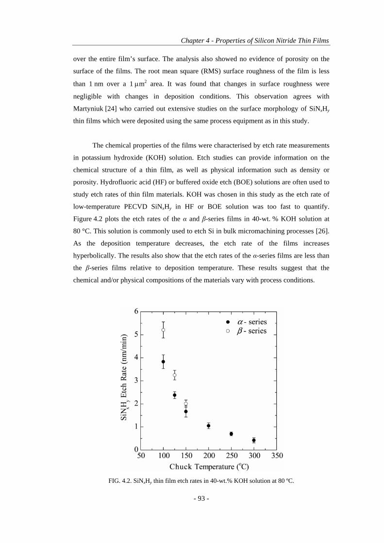
Chapter 4 - Properties of Silicon Nitride Thin Films
- 93 -
over the entire film’s surface. The analysis also showed no evidence of porosity on the
surface of the films. The root mean square (RMS) surface roughness of the film is less
than 1 nm over a 1 µm2 area. It was found that changes in surface roughness were
negligible with changes in deposition conditions. This observation agrees with
Martyniuk [24] who carried out extensive studies on the surface morphology of SiNxHy
thin films which were deposited using the same process equipment as in this study.
The chemical properties of the films were characterised by etch rate measurements
in potassium hydroxide (KOH) solution. Etch studies can provide information on the
chemical structure of a thin film, as well as physical information such as density or
porosity. Hydrofluoric acid (HF) or buffered oxide etch (BOE) solutions are often used to
study etch rates of thin film materials. KOH was chosen in this study as the etch rate of
low-temperature PECVD SiNxHy in HF or BOE solution was too fast to quantify.
Figure 4.2 plots the etch rates of the α and β-series films in 40-wt. % KOH solution at
80 °C. This solution is commonly used to etch Si in bulk micromachining processes [26].
As the deposition temperature decreases, the etch rate of the films increases
hyperbolically. The results also show that the etch rates of the α-series films are less than
the β-series films relative to deposition temperature. These results suggest that the
chemical and/or physical compositions of the materials vary with process conditions.
FIG. 4.2. SiNxHy thin film etch rates in 40-wt.% KOH solution at 80 ºC.

Chapter 4 – Properties of Silicon Nitride Thin Films
- 94 -
4.4. Determination of Density Using the Quartz Crystal Microbalance Method
4.4.1. Basic Formulations for Property Determination
For the quartz crystal microbalance (QCM) method used to determine ρ, the mass
of the film deposited on the quartz crystal can be calculated using the following [2]:
⎟⎟⎠
⎞⎜⎜⎝
⎛ ∆=
qqf F
FMM (4.1)
where Mf is the mass of the deposited film, Mq is the mass of the quartz crystal, ∆F is the
change in resonant frequency of the crystal after the film has been deposited on its
surface, and Fq is the initial resonant frequency of the crystal. The density of the film can
be calculated for given film thickness and area.
4.4.2. Experimental Details
The resonant frequency of a virgin quartz crystal of known surface area was first
measured using an INFICON Thin Film Deposition Controller and then measured again
after the film was deposited on the crystal. The thickness of the film was obtained using a
surface profiler on a witness sample that experienced the same deposition event as the
crystal. For each deposition event, three crystals were positioned inside the chamber in
order to determine the error in the measurement.
4.4.3. Results to the Quartz Crystal Microbalance Method
Figure 4.3 shows the effect of chuck temperature on the density of the SiNxHy thin
films, as determined from the QCM measurements. The error bars represent the standard
deviation in the measurement. It is seen that ρ of the films increases continuously with
increasing deposition temperature and that α-series films exhibit higher ρ values
compared to β-series films. The highest ρ achieved was 2.80 ± 0.05 g/cm3 for a SiNxHy
film deposited at 300 °C, 600 mTorr and 100 W. This is close to the theoretical value of
3.3 g/cm3 for bulk polycrystalline Si3N4 [27]. The lowest ρ achieved was
1.55 ± 0.06 g/cm3 for a SiNxHy film deposited at 100 °C, 875 mTorr and 75 W. Figure 4.3
shows that ρ of the films is highly sensitive to changes in process conditions and that bulk
silicon nitride values cannot accurately represent the true ρ value of the deposited α or β-
series films.

Chapter 4 - Properties of Silicon Nitride Thin Films
- 95 -
4.5. Determination of Young’s Modulus and Poisson’s Ratio Using the Resonance
Method
4.5.1. Basic Formulations for Property Determination
The Young’s modulus of a flat microcantilever beam can be determined from its
bending resonant frequency by rearranging Eqn. (3.47):
224
42
)()(
48nb
n
ftLρLE
βπ
= (4.2)
Similarly, the shear modulus can be determined from its torsional resonant frequency by
rearranging Eqn. (3.48):
222
22
)(4itfti
bLG ρ= , for i = 1, 3, 5... (4.3)
The Poisson’s ratio can be calculated directly from the E and G values by rearranging
Eqn. (3.6):
12
−=GEν (4.4)
FIG. 4.3. Density measurements of α and β-series SiNxHy thin films as a function of chuck
temperature, as determined using the quartz crystal microbalance method.

Chapter 4 – Properties of Silicon Nitride Thin Films
- 96 -
For the first bending and torsional resonant frequencies, substituting Eqns. (4.2) and (4.3)
into Eqn. (4.4) yields:
22 2
4 21
6 1( )
b
t
fLL b fπν
β⎛ ⎞
= −⎜ ⎟⎝ ⎠
(4.5)
Hence the Poisson’s ratio of a microcantilever beam can be determined directly from the
measurements of its bending and torsional resonant frequencies if its length and width are
known. If the thickness and the density of the beam are known, E and G can be
determined using Eqns. (4.2) and (4.3). From the FEM simulations shown in section 3.7,
beams of width 20 µm and of thickness less than 1 µm with L/b ratios greater than 8,
Eqn. (4.5) is accurate to within 7 %, thus providing a good approximation of ν of thin
film microcantilever beams.
4.5.2. Experimental Details
SiNxHy microcantilevers were fabricated on 3-inch (100)-oriented Si wafers using
bulk micromachining techniques, as shown in Fig. 4.4. Due to the high etch rate of low-
temperature PECVD SiNxHy thin films in the KOH solution (see Fig. 4.2), thin layers
(5 nm) of thermally evaporated Cr are deposited before and after the SiNxHy deposition
(Fig. 4.4(a)). The Cr layers act as a barrier between the KOH solution and the SiNxHy thin
film during the etching of the substrate. The films were then patterned (Fig. 4.4(b)) and
the substrates etched in 40-wt. % KOH aqueous solution at 80 °C until the beams were
fully released from the substrate (Fig. 4.4(c)). The Cr layers were then removed in a
hydrochloric acid (HCl) solution (Fig. 4.4(d)). Care was taken not to over-etch the Cr
bottom layer, thus causing undercut at the beams’ supports. This method resulted in
fabricated SiNxHy microcantilevers with constant moment of inertia along their lengths,
thus allowing the application of Eqns. (4.2), (4.3) and (4.5) to determine E, G and ν from
the beams’ resonant frequencies, respectively.
The dimensions of the fabricated microcantilevers ranged from 200-300 µm in
length, 15-25 µm in width and 200-900 nm in thickness. The thickness of the SiNxHy
beams was obtained using a surface profiler on witness samples that experienced the
same deposition event as the fabricated samples. The lengths and widths of the beams
were measured using an optical microscope.
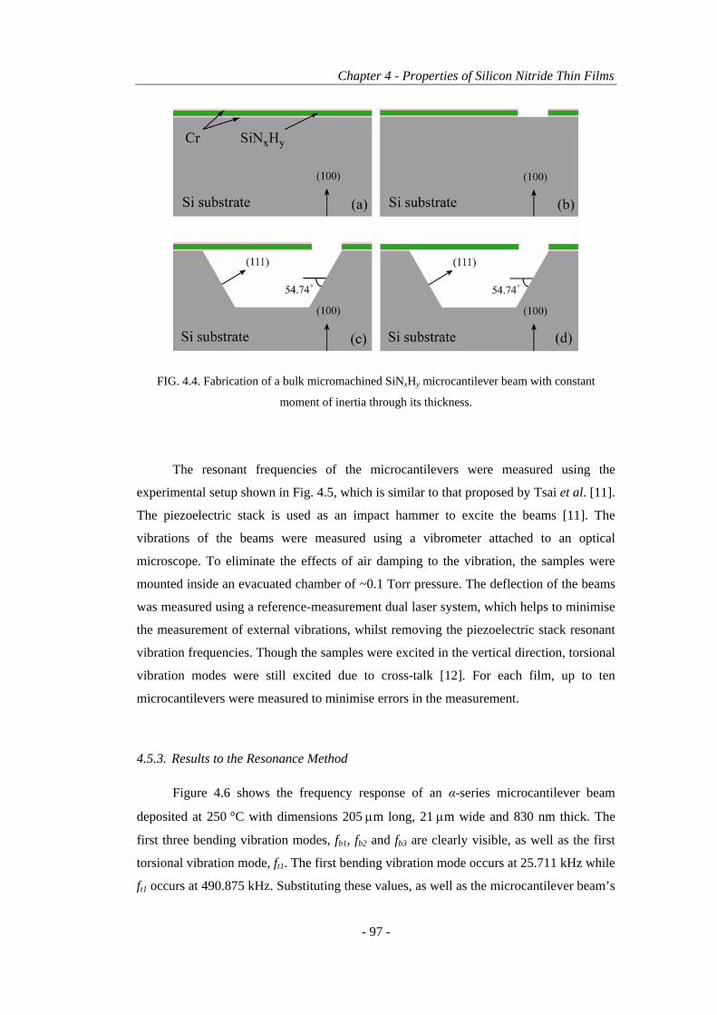
Chapter 4 - Properties of Silicon Nitride Thin Films
- 97 -
The resonant frequencies of the microcantilevers were measured using the
experimental setup shown in Fig. 4.5, which is similar to that proposed by Tsai et al. [11].
The piezoelectric stack is used as an impact hammer to excite the beams [11]. The
vibrations of the beams were measured using a vibrometer attached to an optical
microscope. To eliminate the effects of air damping to the vibration, the samples were
mounted inside an evacuated chamber of ~0.1 Torr pressure. The deflection of the beams
was measured using a reference-measurement dual laser system, which helps to minimise
the measurement of external vibrations, whilst removing the piezoelectric stack resonant
vibration frequencies. Though the samples were excited in the vertical direction, torsional
vibration modes were still excited due to cross-talk [12]. For each film, up to ten
microcantilevers were measured to minimise errors in the measurement.
4.5.3. Results to the Resonance Method
Figure 4.6 shows the frequency response of an α-series microcantilever beam
deposited at 250 °C with dimensions 205 µm long, 21 µm wide and 830 nm thick. The
first three bending vibration modes, fb1, fb2 and fb3 are clearly visible, as well as the first
torsional vibration mode, ft1. The first bending vibration mode occurs at 25.711 kHz while
ft1 occurs at 490.875 kHz. Substituting these values, as well as the microcantilever beam’s
FIG. 4.4. Fabrication of a bulk micromachined SiNxHy microcantilever beam with constant
moment of inertia through its thickness.

Chapter 4 – Properties of Silicon Nitride Thin Films
- 98 -
dimensions and density value (obtained using the QCM method) into Eqns. (4.2), (4.3)
and (4.5) yields calculated E, G and ν values equal to 182 GPa, 72.6 GPa and 0.25,
respectively. Substituting the calculated E and G values into Eqn. (4.4) yields a ν value
equal to 0.25, which agrees with the ν value calculated using Eqn. (4.5).
Figure 4.7 shows the calculated E, G and ν values of the α and β-series thin films
as a function of chuck temperature using the resonance method. The density of the films
required to determine E and G were obtained from the QCM measurements. The error
bars represent the standard deviations in the measurements. The values shown were
calculated using the first bending and torsional vibration frequencies. It is evident that E
and G of the films increase continuously with increasing deposition temperature. The α-
series thin films have higher E and G values compared to β-series films, relative to chuck
temperature. The highest E and G values achieved were 193 ± 7 GPa and 77 ± 3 GPa,
respectively, for SiNxHy films deposited at 300 °C, 600 mTorr and 100 W. This E value is
still far below that of bulk polycrystalline Si3N4, which is 304 GPa [27]. The lowest E and
G values achieved were 54 ± 6 GPa and 22 ± 3 GPa, respectively, for SiNxHy films
deposited at 100 °C, 875 mTorr and 75 W.
FIG. 4.5. Schematic diagram of the resonant frequency method experimental setup.

Chapter 4 - Properties of Silicon Nitride Thin Films
- 99 -
The ν values show little difference between the α-series and β-series films. Though
the relative errors are large, both sets of films show clearly that ν increases with
increasing chuck temperature for temperatures below 200 ºC. For films deposited above
200 °C, the measured Poisson’s ratio appears to be independent with changes in chuck
temperature. At these temperatures, a Poisson’s ratio of approximately 0.25 is realised.
The highest ν value achieved was 0.26 ± 0.01 for SiNxHy films deposited at 250 °C,
600 mTorr and 100 W. This ν value is close to that of bulk polycrystalline Si3N4, which is
0.27 [27]. The lowest ν value achieved was 0.20 ± 0.01 for SiNxHy films deposited at
100 °C, 875 mTorr and 75 W.
Similarly to the ρ measurements presented in Section 4.4, the E, G and ν of α and
β-series films are highly sensitive to process conditions. It is also obvious that bulk
silicon nitride values cannot accurately represent the true E, G and ν values of the
deposited α or β-series films. As deposition temperature increases, however, the E, G and
ν values of the films approach that of the bulk values.
FIG. 4.6. Frequency response of a 250 ºC deposited α-series microcantilever beam of
dimensions 205 µm × 21 µm × 830 nm. fb1, fb2 and fb3 represent the first three bending vibration
modes while ft1 represents the first torsional vibration mode.

Chapter 4 – Properties of Silicon Nitride Thin Films
- 100 -
FIG. 4.7. Resonant method measurements showing (a) E, (b) G, and (c) ν versus changes in
chuck temperature for α and β-series films.

Chapter 4 - Properties of Silicon Nitride Thin Films
- 101 -
4.6. Determination of Young’s Modulus Using Nanoindentation and
Microcantilever Beam Bending Methods
4.6.1. Basic Formulations for Property Determination
When an indenter of known dimensions is pressed onto the surface of a specimen,
the force on the indenter will increase with increasing penetration depth. If the projected
area of the indenter increases with increasing indentation depth (for example, a spherical
or pyramidal shaped indenter), this force increases non-linearly. For a purely elastic
material, the force induced onto the indenter relative to indentation depth will be the same
for both loading and unloading events. For a purely inelastic (i.e. plastic) material, no
force will be induced onto the indenter during an unloading event. Generally, materials
behave both elastically and inelastically, and the loading-unloading curves of an indented
material will look similar to that depicted in Fig. 4.8(a). In this case a SiNxHy thin film
has been indented with a Berkovich tip, which is commonly used in nanoindentation
experiments and is illustrated in Fig. 4.8(b) [28]. For the case where plastic deformation
occurs, the indentation event will leave an impression in the specimen and its height is
equal to the difference in the loading-unloading curve at zero applied load (denoted hr in
Fig. 4.8(a)).
During a loading event, both elastic and plastic deformation occurs. During
unloading, the force induced onto the tip by the film is purely elastic, and is due to the
relaxation of elastic strains within the material [29]. Hence, from nanoindentation
experiments, E is determined from the unloading contact stiffness, S, which can be
obtained from the slope of the initial portion of the unloading curve [6]:
dhdPS = (4.6)
From the parameter S, the reduced modulus Er, which is a measure of the
combined elastic response of the specimen and the indenter, can be determined as:
2r
SEA
πη
= ⋅ (4.7)
which in turn can be related to the Young’s modulus of the sample in:
22 11 1 D
r DE E Eνν −−
= + (4.8)

Chapter 4 – Properties of Silicon Nitride Thin Films
- 102 -
In the equations above, P is the applied load, h is the tip displacement, A is the contact
area, η is a constant depending on the geometry of the indenter, ν and E are the Poisson’s
ratio and the Young’s modulus of the specimen, νD and ED are the Poisson’s ratio and the
Young’s modulus of the diamond tip. Here, νD and ED are equal to 0.07 and 1140 GPa,
respectively, and for the Berkovich indenter tip η = 1.034.
The method described above is known as the Oliver and Pharr [6, 29] method,
which is a refinement of the Doerner and Nix [30] approach. The Oliver and Pharr
method is now the most commonly used method of analysis to determine E from
nanoindentation loading data [29]. It has recently been shown however that the
determination of E using nanoindentation of a thin film material deposited onto a
FIG. 4.8. Nanoindentation of a SiNxHy thin film showing, (a) a typical load versus tip
displacement curve, and (b) SEM image of a Berkovich indenter tip [28].

Chapter 4 - Properties of Silicon Nitride Thin Films
- 103 -
substrate is directly dependent on the thickness of the film and the Young’s modulus of
the substrate (Es) relative to the Young’s modulus of the film (Ef). When nanoindentation
is performed on a film deposited on a substrate, such that Es>Ef, the calculated E using
the Oliver and Pharr method increases with increasing indentation depth towards Es. For
the case where Es<Ef, the calculated Er decreases with increasing indentation depth
towards Es. Previous methods used to negate the effect of the substrate on the calculated
Ef have simply been to neglect all values of Ef calculated from indentation depths greater
than 10 % of the film thickness [31, 32]. Jung et al. [5] provides a more elegant approach
whereby the contributions from substrate deformation on the calculated Ef can be
accounted for. In this method, Ef is determined using the following equations:
L
s
fs E
EEE ⎟⎟
⎠
⎞⎜⎜⎝
⎛= (4.9)
1
1+D
LhCt
=⎡ ⎤⎛ ⎞⎢ ⎥⎜ ⎟
⎝ ⎠⎢ ⎥⎣ ⎦
(4.10)
where h and t are the indentation depth and film thickness, respectively and C and D are
adjustable coefficients. Equations (4.9) and (4.10) satisfy the boundary conditions:
h/t→0, E=Ef and h/t→∞, E=Es. Hence Ef is determined from multiple indentations carried
out over a range of indentation depths. By plotting E verses h and fitting the data with
Eqns. (4.9) and (4.10), Ef can be determined.
As outlined in Chapter 3, the Young’s modulus can also be inferred from the
deflection of a microcantilever. When a nanoindenter is used to deflect a microcantilever
beam, it acts as point load. For a beam with constant moment of inertia through its length,
E of the beam can be calculated by rearranging Eqn. (3.25):
3
23
4 (1 )L FEbt w
ν⎛ ⎞= −⎜ ⎟⎝ ⎠
(4.11)
In this case, F/w is equal to the slope of the applied force versus displacement curve of
the tip of the nanoindenter, and L is the distance from the base of the beam to the tip of
the nanoindenter. Similarly for a tapered beam, E is calculated by rearranging
Eqn. (3.26):
23 2
(3 2 )6 2 ln(1 ) (1 )( )
t
t t
mL mL tmL FEbm t t mL w
ν⎛ ⎞+⎛ ⎞ ⎛ ⎞= + − −⎜ ⎟⎜ ⎟ ⎜ ⎟+⎝ ⎠ ⎝ ⎠⎝ ⎠
(4.12)

Chapter 4 – Properties of Silicon Nitride Thin Films
- 104 -
4.6.2. Experimental Details
Nanoindentation was used to determine E of α-series thin films using a Hysitron
Triboscope III nanomechanical testing instrument, connected to a Digital Instruments
atomic force microscope (AFM) with a Berkovich indenter tip. The indentation profile
used is shown in Fig. 4.9. A holding time of 10 s at the maximum load was used to
eliminate any creep effect on the measurements. For each film, three sets of up to 100
indents were performed with varying indentation loads ranging from 100 µN up to
9000 µN.
For the microcantilever beam bending method used to determine E, the SiNxHy thin
films were patterned into microcantilever beams using the same bulk micromachining
methods shown in Fig. 4.4, except the Cr layers were not included. The SiNxHy thin films
were thus exposed to KOH during the substrate etching process, which resulted in tapered
beams. The microcantilevers were fabricated with widths ranging from 15 µm to 30 µm
and in various lengths ranging from 30 µm to 150 µm. The thicknesses of the beams
ranged from 300 nm to 1000 nm.
Bending tests of the microcantilever beams were carried out using the Hysitron
Triboscope III nanomechanical testing instrument, connected to a Digital Instruments
FIG. 4.9. Indentation profile used for the nanoindentation experiments.
Chapter 4 - Properties of Silicon Nitride Thin Films
- 105 -
AFM. The microcantilevers were initially scanned using the AFM, thus creating an
image, which enabled precise positioning of the nanoindenter tip on the microcantilevers.
The beams were deflected with a conical diamond tip of 20 µm tip radius and a 90° cone
angle. The large tip radius ensures that no indentation of the beam occurred during
bending. The beams were deflected up to 1 µm and the load versus tip displacement was
recorded. For each film, up to 10 microcantilevers of varying dimensions were deflected.
4.6.3. Nanoindentation and Microcantilever Beam Bending Results
The results of the nanoindentation experiments for three α-series thin films
deposited at different chuck temperatures are shown in Fig. 4.10, where E is a function of
normalised indentation depth. The dashed reference line in Fig. 4.10 marks the value of
the Young’s modulus of the Si substrate, ESi, as determined from nanoindentation
experiments. This value is similar to that found in the literature [33]. It is seen that for all
three films, E approaches ESi with increasing indentation depth. The power-law method
proposed by Jung et al. [5] was used to determine E from the film/substrate composite to
the values for the SiNxHy films. From these plots, the Young’s modulus of the 125 ºC,
150 ºC and 200 ºC deposited films were calculated to be 98 GPa, 131 GPa and 162 GPa,
respectively.
Figure 4.11(a) shows an SEM top view image of three released microcantilevers of
25×125 µm in dimensions. It is seen that they are flat and free of any stress gradient.
During the wet release process, etching occurred preferentially on selected atomic planes
in the Si substrate, with the etching front propagating from the tip to the base of the
beams. As the selectivity of the KOH etchant is not infinite, i.e. some slow etching also
occurred on the SiNxHy thin film, a thickness gradient resulted along the length of the
beam [11]. The exact amount of tapering, i.e. the thickness at the base and the tip of the
beam was determined using SEM. An SEM image showing the thickness of a
microcantilever beam near its base is illustrated in Figure 4.11(b). Care was taken not to
etch the samples for too long in an attempt to minimise the amount of undercut at the base
of the beam.
Figure 4.12 illustrates the applied load of the nanoindenter tip relative to its
displacement on an α-series microcantilever beam deposited at 300 °C. The curve is
linear, indicating that the deformation of the beam was totally within the elastic regime.

Chapter 4 – Properties of Silicon Nitride Thin Films
- 106 -
As the beams were tapered, the slope of the curve in Fig. 4.12 is equivalent to the (F/w)
term in Eqn. (4.12). The actual dimensions of the deflected beam were 19 µm in width,
38 µm in length and 900 nm in thickness at its base and 830 nm at its end. The thickness
variation of the beam across its length was determined using SEM. In this particular
example, the length from the base of the beam to the loading point was 32 µm. Using the
calculated ν value of the film determined using the resonance method, the Young’s
modulus of this beam was determined using Eqn. (4.12) to be 193 GPa.
The average E values for α-series thin films calculated from microcantilever beam
bending tests and nanoindentation measurements are shown in Fig. 4.13. It is evident that
the two methods, as well as the E values calculated using the resonance method, exhibited
excellent agreement. The Young’s modulus was found to increase rapidly with increasing
chuck temperature. The Young’s modulus appeared to reach saturation at above 200 °C.
The highest E achieved was 195 GPa at the deposition temperature of 300 °C. For the
film deposited at 100 °C, E was measured to be 83 GPa, ~43% of that of the film
deposited at 300 °C.
FIG. 4.10. Normalised nanoindentation data of three α-series thin films deposited at varying
chuck temperatures. On the x-axis, h/t is the ratio of indentation depth (h) to film thickness (t).
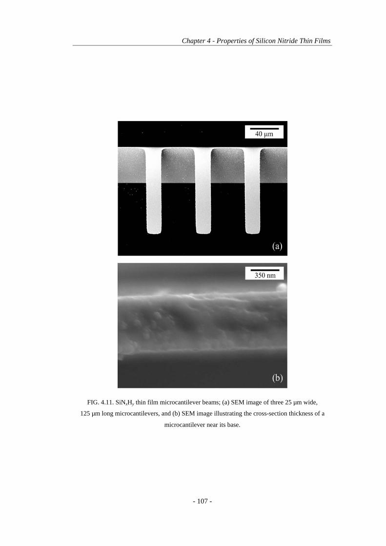
Chapter 4 - Properties of Silicon Nitride Thin Films
- 107 -
FIG. 4.11. SiNxHy thin film microcantilever beams; (a) SEM image of three 25 µm wide,
125 µm long microcantilevers, and (b) SEM image illustrating the cross-section thickness of a
microcantilever near its base.
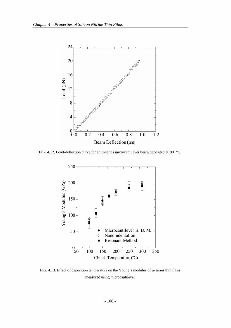
Chapter 4 – Properties of Silicon Nitride Thin Films
- 108 -
FIG. 4.12. Load-deflection curve for an α-series microcantilever beam deposited at 300 °C.
FIG. 4.13. Effect of deposition temperature on the Young’s modulus of α-series thin films
measured using microcantilever
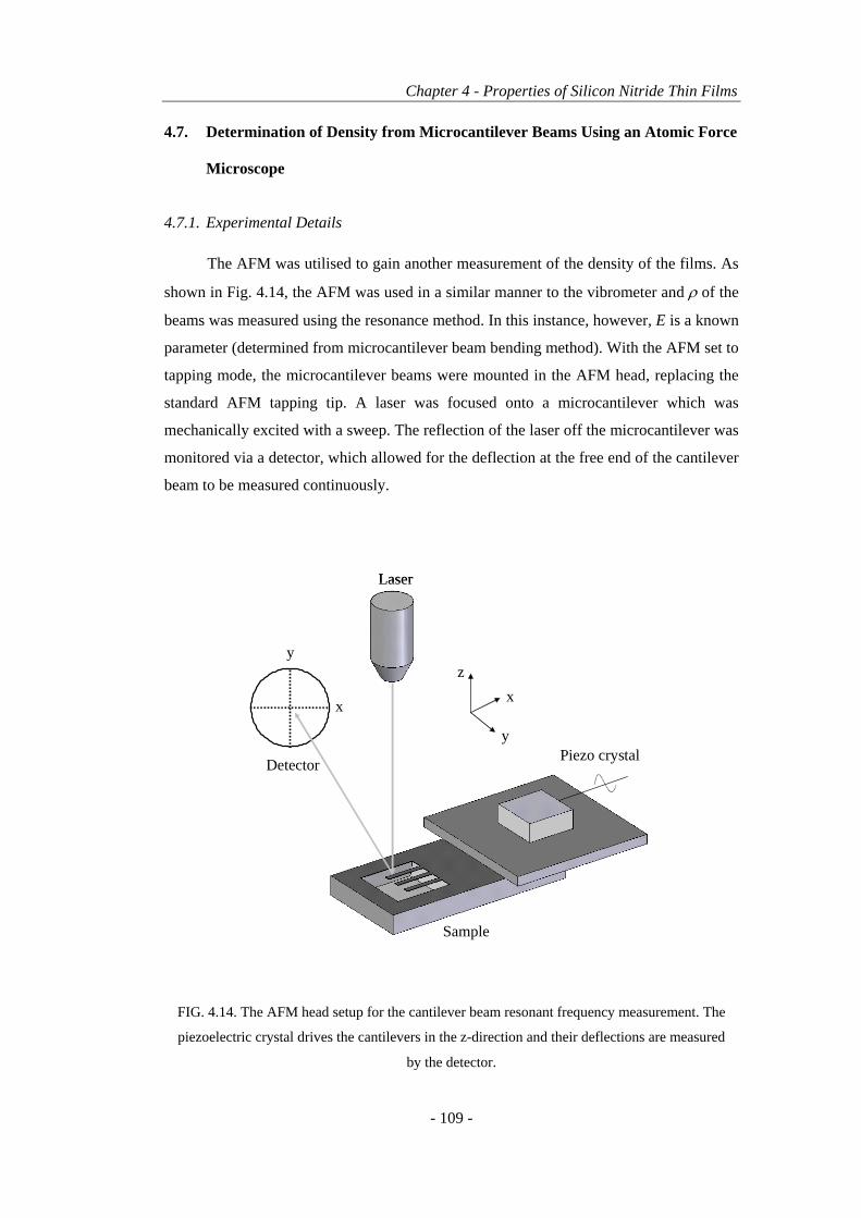
Chapter 4 - Properties of Silicon Nitride Thin Films
- 109 -
4.7. Determination of Density from Microcantilever Beams Using an Atomic Force
Microscope
4.7.1. Experimental Details
The AFM was utilised to gain another measurement of the density of the films. As
shown in Fig. 4.14, the AFM was used in a similar manner to the vibrometer and ρ of the
beams was measured using the resonance method. In this instance, however, E is a known
parameter (determined from microcantilever beam bending method). With the AFM set to
tapping mode, the microcantilever beams were mounted in the AFM head, replacing the
standard AFM tapping tip. A laser was focused onto a microcantilever which was
mechanically excited with a sweep. The reflection of the laser off the microcantilever was
monitored via a detector, which allowed for the deflection at the free end of the cantilever
beam to be measured continuously.
y
xz
x
y
Laser
Detector
Sample
Piezo crystaly
xz
x
y
Laser
Detector
Sample
Piezo crystal
FIG. 4.14. The AFM head setup for the cantilever beam resonant frequency measurement. The
piezoelectric crystal drives the cantilevers in the z-direction and their deflections are measured
by the detector.

Chapter 4 – Properties of Silicon Nitride Thin Films
- 110 -
4.7.2. Results to the Density Measurements
Figure 4.15 shows the effect of chuck temperature on the density of α-series thin
films, as determined from resonating tapered microcantilever beams measured using the
AFM. For comparison, ρ values obtained using the QCM method are also plotted. As
Eqn. (4.2) is only applicable for a beam whose thickness is uniform across its length, the
density of the beams was determined using the commercial finite element modelling
package ANSYS. A modal analysis for a simple microcantilever beam of variable
thickness across its length was modelled using shell elements. Using the measured first
order bending resonant frequencies of microcantilever beams obtained from the AFM, as
well as their measured E values determined from microcantilever beam bending tests, ρ
could be extracted. The results presented in Fig. 4.15 show that both the QCM method
and the AFM method shown excellent agreement. It is seen that ρ of the films increased
continuously with increasing deposition temperature. The highest ρ achieved was
2.9 g/cm3 at the deposition temperature of 300 °C. For the film deposited at 100 °C the
density was estimated as 1.8 g/cm3, ~64% of that of the film deposited at 300 °C.
FIG. 4.15. Effect of chuck temperature on density of α-series thin films, as determined from
resonating, tapered microcantilever beams. The resonant modes of the beams were measured
using an AFM. For comparison, density measurements obtained using the QCM method are
also plotted.

Chapter 4 - Properties of Silicon Nitride Thin Films
- 111 -
It has been reported in the literature that the density of PECVD SiNxHy films are
dependent on film thickness [34]. A variation in ρ through the thickness of an amorphous
CVD deposited thin film suggests that during film growth, a variation in process
conditions has occurred. For example, the temperature of the substrate may increase
during deposition due to ion bombardment. Also, an increase in chamber pressure during
deposition can result from the out-gassing of chamber deposits. This can occur if the
chamber is not cleaned before deposition. For very dirty chambers, the increase in
pressure can be significant.
To determine whether the mechanical and physical properties of PECVD SiNxHy
thin films are dependent on film thickness, the density of three α-series films of different
thicknesses, all deposited at the same temperature of 200 °C, were measured. Through
microcantilever beam bending measurements, Young’s modulus measurements were also
carried out on three α-series thin films of different thicknesses, also deposited at the same
temperature of 200 °C. It is important to note that for these film depositions, as well as
for all PECVD SiNxHy depositions carried out in this study, the PECVD chamber was
thoroughly cleaned before each deposition event. Figure 4.16 shows the E and ρ
measurements as a function of film thickness. The E and ρ values were measured from
bending and resonating microcantilever beams, respectively. The resonant frequencies
were measured using the AFM. It is evident that the variation of E and ρ with changes in
film thickness is within the error of the measurement, which suggests that during each
deposition event the variation in process conditions is negligible.
4.8. Determination of Residual Stress Using the Substrate Curvature Method
4.8.1. Basic Formulations for Property Determination
The residual stress in a film on a film-substrate assembly was determined using the
curvature measurement method. The relationship between the residual stress in the film
and the induced curvature of the substrate is expressed in the Stoney formula [35]:
2
6 (1 )s s
s f
E tR t
σν
=−
(4.13)
where Es and νs are the Young’s modulus and the Poisson’s ratio of the substrate,
respectively, ts and tf are the thickness of the substrate and film, respectively and R is the
radius of curvature of the assembly. This method is true only for situations where ts>>tf
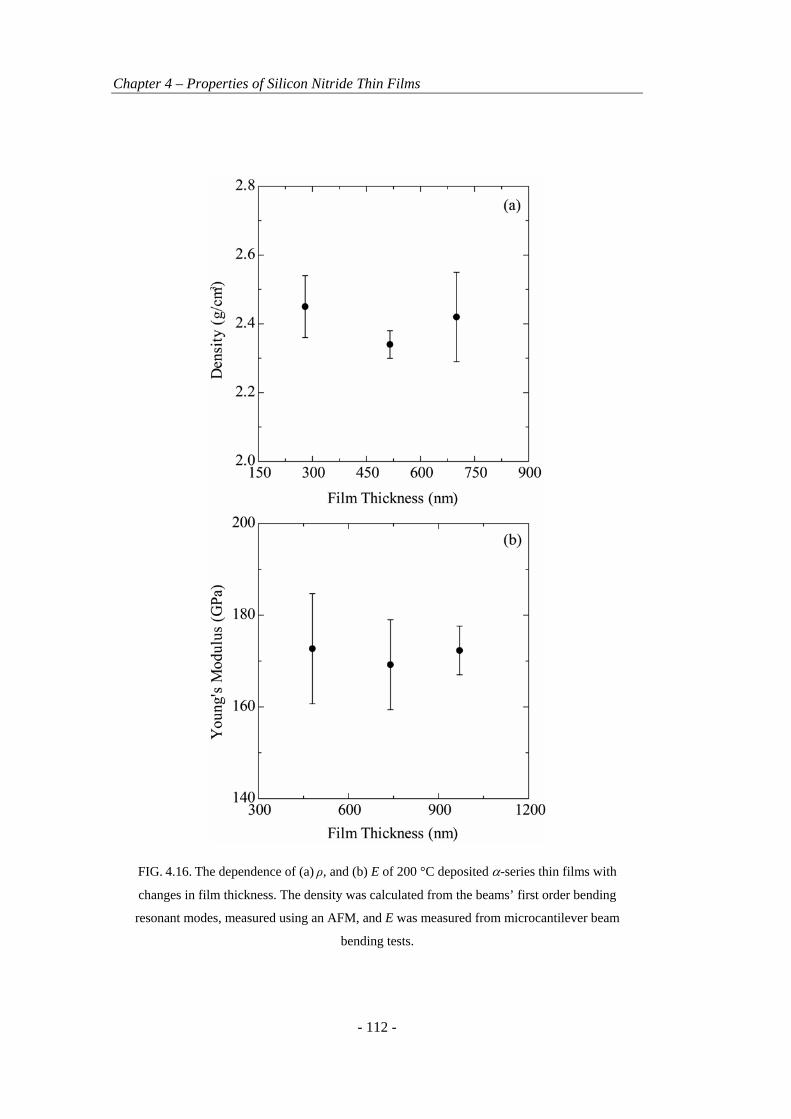
Chapter 4 – Properties of Silicon Nitride Thin Films
- 112 -
FIG. 4.16. The dependence of (a) ρ, and (b) E of 200 °C deposited α-series thin films with
changes in film thickness. The density was calculated from the beams’ first order bending
resonant modes, measured using an AFM, and E was measured from microcantilever beam
bending tests.
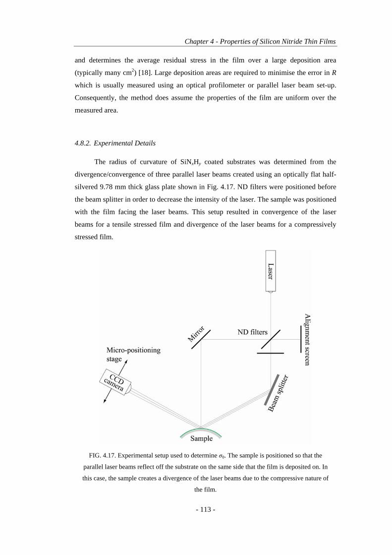
Chapter 4 - Properties of Silicon Nitride Thin Films
- 113 -
and determines the average residual stress in the film over a large deposition area
(typically many cm2) [18]. Large deposition areas are required to minimise the error in R
which is usually measured using an optical profilometer or parallel laser beam set-up.
Consequently, the method does assume the properties of the film are uniform over the
measured area.
4.8.2. Experimental Details
The radius of curvature of SiNxHy coated substrates was determined from the
divergence/convergence of three parallel laser beams created using an optically flat half-
silvered 9.78 mm thick glass plate shown in Fig. 4.17. ND filters were positioned before
the beam splitter in order to decrease the intensity of the laser. The sample was positioned
with the film facing the laser beams. This setup resulted in convergence of the laser
beams for a tensile stressed film and divergence of the laser beams for a compressively
stressed film.
FIG. 4.17. Experimental setup used to determine σ0. The sample is positioned so that the
parallel laser beams reflect off the substrate on the same side that the film is deposited on. In
this case, the sample creates a divergence of the laser beams due to the compressive nature of
the film.

Chapter 4 – Properties of Silicon Nitride Thin Films
- 114 -
The substrate’s radius of curvature can be determined using the following
equation [17]:
D
DLR∆
=θcos
2 (4.14)
where L is the distance from the CCD camera to the sample, θ is the angle of incidence, D
is the interspot distance of the parallel beams and ∆D is the change in the interspot
distance of the reflected beams at the CCD camera. In this particular setup, D was equal
to 6.5 mm. Double-sided polished (100)-oriented Si wafers of thickness 100 µm were
used. Prior to SiNxHy deposition the wafers were dipped in an HF solution to remove the
native oxide layer and then cleaved into rectangles of size 60 mm × 5 mm. The curvatures
of the cleaved Si samples were then measured using the apparatus shown in Fig. 4.17 to
ensure they were optically flat. Three cleaved wafers were positioned in the chamber
during each deposition event to determine the error in the measurement.
4.8.3. Results to the Substrate Curvature Method
Figure 4.18 shows the effect of chuck temperature on the residual stresses of the α
and β-series films. The standard deviation errors of the measurements are smaller in
magnitude than the size of the symbols used to represent the measurement points and thus
FIG. 4.18. Residual stress measurements of α and β−series SiNxHy thin films determined using
the substrate curvature method. Negative σ0 values represent compressive stress.
Chapter 4 - Properties of Silicon Nitride Thin Films
- 115 -
are not shown. It is seen that the residual stresses increase with increasing deposition
temperature for both α- and β-series films. The magnitude of the stress in α-series films
is greater than in β-series films whereas β-series films have higher tensile stress. The
highest compressive residual stress achieved was 133 MPa for SiNxHy films deposited at
100 °C, 600 mTorr and 100 W. The highest tensile residual stress achieved was 59 MPa
for SiNxHy films deposited at 150 °C, 875 mTorr and 75 W.
4.9. Determination of Young’s Modulus, Residual Stress and Poisson’s Ratio
Using the Bulge Test
4.9.1. Basic Formulations for Property Determination
For square and rectangular thin-film membranes with zero residual stress that are
constrained around the perimeter, the bulge height at their central point of the square is
related to the applied pressure by Eqns. (3.27) and (3.28). If both a square and an infinite
rectangular membrane are fabricated on the same substrate and from the same thin film
and that they are both subjected to the same uniform pressure, then Eqns. (3.27) and
(3.28) may be combined to yield:
43
34)1)(( ⎟⎟
⎠
⎞⎜⎜⎝
⎛⎟⎟⎠
⎞⎜⎜⎝
⎛=+
r
s
s
r
aa
wwf νν (4.15)
Furthermore, if the membranes are designed such that as = ar, then Eqn. (4.15) simplifies
to:
3
34)1)(( ⎟⎟
⎠
⎞⎜⎜⎝
⎛=+
s
r
wwf νν (4.16)
Equation (4.16) demonstrates that the wr/ws ratio is solely determined by the Poisson’s
ratio of the film, and is independent of the applied pressure P.
For the case where a membrane contains a tensile residual stress σ0, the
relationship between the applied pressure and the central point bulge height of a square
and an infinite rectangular membrane are given by Eqns. (3.34) and (3.35). As mentioned
in section (3.4), it is evident that for large bulge heights, Eqns. (3.34) and (3.35) are
reduced to Eqns. (3.27) and (3.28), respectively, since the linear terms become negligible.
Hence, if a square membrane and an infinite rectangular membrane of the same
dimension as = ar are fabricated on the same substrate and from the same thin film having

Chapter 4 – Properties of Silicon Nitride Thin Films
- 116 -
the same residual tensile stress σ0, and are tested under the same uniform pressure, then ν
can be calculated from the ratio of wr/ws at high pressures using Eqn. (4.16). However, for
thin films with relatively low failure strengths, such as low-temperature PECVD SiNxHy
films, large bulge heights cannot be achieved prior to failure. In such cases, ν needs to be
determined by measuring ws and wr over a range of pressures, and curve-fitting the data to
the following equations:
321 ssss wAwAP += (4.17)
321 rrrr wAwAP += (4.18)
where A1s, A2s, A1r and A2r are fitting parameters. Referring to Eqns. (3.34) and (3.35), it
is evident that:
20
1s
ss atcA σ
= (4.19.a)
)1(
)(42 νν−
=s
s aEtfA (4.19.b)
20
1r
rr atcA σ
= (4.19.c)
)1(3
4242 ν−
=r
r aEtA (4.19.d)
For the special case when as=ar, dividing A2s by A2r yields:
⎟⎟⎠
⎞⎜⎜⎝
⎛=+
r
s
AA
f2
2
34)1)(( νν (4.20)
Using Eqn. (4.20), ν can be determined directly from the A2s / A2r ratio, and is independent
of the initial tensile residual stress. This implies that Eqn. (4.20) is applicable for both
stress-free membranes and membranes containing tensile residual stress. Equation (4.19)
can also be used to determine E and σ0 if the membrane dimensions are accurately known.
By dividing A1s by A1r, the following relationship can also be derived:
02
1
1 02
1.6965s
ss s
r rr
r
tcaA c
A ctca
σ
σ
⎛ ⎞⎜ ⎟⎛ ⎞ ⎝ ⎠= = =⎜ ⎟ ⎛ ⎞⎝ ⎠⎜ ⎟⎝ ⎠
(4.21)
Equation (4.21) will hold true for any thin film material tested so long as as = ar and the
film thickness and residual stress is uniform. Consequently, Eqn. (4.21) can be used as a
Chapter 4 - Properties of Silicon Nitride Thin Films
- 117 -
measure of possible experimental errors associated with thin film uniformity and
membrane dimensions.
The analysis procedure discussed above can be used to determine ν, E and σ0 for
any thin film membrane material. However, Vlassak and Nix [14] have suggested that
Eqns. (3.27) and (3.28) become invalid for σ0 values above 500 MPa. In a recent study,
Mitchell et al. [36] were unable to determine ν using the bulge test for 3C-SiC films that
were known to exhibit residual tensile stress greater than 300 MPa. In the present study,
only tensile low stress thin films have been used for all bulge test experiments.
4.9.2. Experimental Details
Similar to the bulk micromachining processes described above, square and
rectangular SiNxHy thin film membranes were patterned and released from (100)-oriented
Si substrates. As the bulge test is only applicable to tensile stressed thin films, an α-series
film deposited at 205 °C and a β-series film deposited at 125 °C are fabricated into square
and rectangular membranes. A fully-fabricated membrane is shown schematically in
Fig. 4.19(a). CF4 plasma was used to dry etch the top SiNxHy film, followed by wet
etching of the Si substrate in 40-wt. % KOH solution at 80 °C. As expected, some etching
of the SiNxHy films did occur in the KOH solution, however, note that the samples were
completely immersed in the KOH solution, and etching was terminated immediately on
removal of the Si substrate. In order to accurately determine E and σ0 of the thin films
(see Eqn. (4.19)), their thickness needed to be measured after membrane release. This was
achieved by wet etching an area of the SiNxHy thin film that was still attached to the
substrate and using a surface profiler to measure the SiNxHy step height.
Multiple pairs of square and rectangular SiNxHy membranes were fabricated on 3-
inch Si wafers. The square membranes were approximately 1900×1900 µm in size, and
the rectangular membranes had dimensions of approximately 1900×9000 µm. For each
set of square and rectangular membranes, the variation in ar relative to as was measured
to be less than ±0.2%.
Bulge height measurements of the pressurized thin film membranes were carried
out using a Zygo Maxim-GP optical profilometer, and the experimental setup is shown in
Fig. 4.19(b). The samples were mounted on the pressure chamber with an adhesive
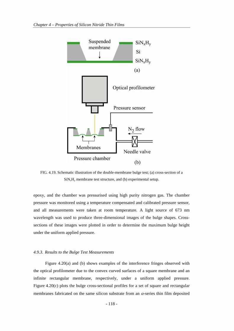
Chapter 4 – Properties of Silicon Nitride Thin Films
- 118 -
epoxy, and the chamber was pressurised using high purity nitrogen gas. The chamber
pressure was monitored using a temperature compensated and calibrated pressure sensor,
and all measurements were taken at room temperature. A light source of 673 nm
wavelength was used to produce three-dimensional images of the bulge shapes. Cross-
sections of these images were plotted in order to determine the maximum bulge height
under the uniform applied pressure.
4.9.3. Results to the Bulge Test Measurements
Figure 4.20(a) and (b) shows examples of the interference fringes observed with
the optical profilometer due to the convex curved surfaces of a square membrane and an
infinite rectangular membrane, respectively, under a uniform applied pressure.
Figure 4.20(c) plots the bulge cross-sectional profiles for a set of square and rectangular
membranes fabricated on the same silicon substrate from an α-series thin film deposited
FIG. 4.19. Schematic illustration of the double-membrane bulge test; (a) cross-section of a
SiNxHy membrane test structure, and (b) experimental setup.

Chapter 4 - Properties of Silicon Nitride Thin Films
- 119 -
FIG. 4.20. Optical profilometer measurements with 673 nm illumination showing; (a)
interference fringes of the middle section of a square membrane under a uniform applied
pressure, (b) interference fringes of the middle section of an infinite rectangular membrane
under a uniform applied pressure, and (c) cross-sectional bulge profiles through the centre (see
insert) of a square and a rectangular membrane under 300 Pa of pressure for a 305 nm thick
PECVD α-series thin film deposited at 205 °C.

Chapter 4 – Properties of Silicon Nitride Thin Films
- 120 -
at 205 °C. The applied pressure corresponding to the two profiles was 300 Pa. The inset
illustrates a top view of the membranes, indicating the positions of the bulge cross-
sectional profiles. It is evident that under the same applied pressure, the square membrane
produced a lower bulge profile compared to the infinite rectangular membrane, which is
due to the greater degree of constraint to bulging that result from the fixed edges of the
square membrane.
It was found that for rectangular membranes, the bulge profile across the width at
any pressure was accurately described by a parabola, with correlation coefficients better
than 0.999. This observation agrees with Kalkman et al. [20] who found the same
parabolic correlation for rectangular free-standing tungsten thin films. However, for the
square membranes, it was found that a fourth order polynomial was well-suited to
describing the bulge profile across the centre at any pressure.
Figure 4.21 shows the relationship between bulge height and applied pressure for two
pairs of membranes fabricated from a β-series thin film deposited at 125 °C (Fig. 3(a))
and an α-series thin film deposited at 205 °C (Fig. 3(b)). The data were fitted using
Eqns. (4.17) and (4.18), with the fitting parameters summarized in Table 4.2. Substituting
the A2s/A2r ratios for this particular set of membranes into Eqn. (4.20) yields a Poisson’s
ratio of 0.24 for the 125 °C deposited film and 0.25 for the 205 °C deposited film, when
using the Vlassak and Nix expression for f(ν) in Table 3.1 [14]. The SiNxHy thicknesses
of these two sets of membranes were measured to be 680 nm and 305 nm for the 125 °C
and 205 °C deposited films, respectively. These thickness values and the parameters
listed in Table 4.2 were substituted into Eqn. (4.19) to determine the Young’s modulus, E,
and residual stress, σ0, for each film. The calculated E values for this particular set of
membranes were thus calculated to be 82 GPa and 146 GPa for the 125 °C deposited film
and the 205 °C deposited film, respectively. The corresponding σ0 values were calculated
to be 4.3 MPa and 32 MPa for the 125 °C deposited film and the 205 °C deposited film,
respectively.
Table 4.2
Fitting parameters for the curves shown in Fig. 4.21. SiNxHy Deposition
Temp. (°C) A1s
(kPa/µm) A2s
(kPa/µm3) A1r
(kPa/µm) A1r
(kPa/µm3) 125 1.094×10⁻² 1.630×10⁻⁴ 6.462×10⁻³ 9.490×10⁻⁵ 205 3.426×10⁻² 1.259×10⁻⁴ 2.114×10⁻² 7.291×10⁻⁵

Chapter 4 - Properties of Silicon Nitride Thin Films
- 121 -
FIG. 4.21. Measured relationship between applied pressure and bulge height for square and
rectangular β and α-series thin film membranes deposited at; (a) 125 °C, and (b) 205 °C,
respectively. The solid lines represent fits to the data using Eqns. (4.17) and (4.18) and the
fitting parameters listed in Table 4.2.

Chapter 4 – Properties of Silicon Nitride Thin Films
- 122 -
Figure 4.22 shows the measured relationships between wr and ws extracted from
the fits shown in Fig. 4.21 for the two films. The dashed lines in both plots are linear,
representing the wr/ws ratio under the condition of zero residual stress: that is σ0=0, as
represented by Eqn. (4.16). It needs to be pointed out that the slope of all the curves in
Fig. 4.22 is always greater than unity. This is due to the bulge height of an infinite
rectangular membrane being always greater than that of a square membrane. From the
data in Fig. 4.22, it is evident that the relationship between wr and ws is non-linear for low
bulge heights, with the experimental curves deviating from the reference dashed lines.
This implies that the films contain residual tensile stresses, which act to restrict bulging of
the membranes.
The curve for the 205 °C deposited film deviates further from the reference line in
comparison to the 125 °C deposited film, which is consistent with the fact that the 205 °C
deposited film had a higher tensile stress than the 125 °C deposited film. The
experimental curves appear above the reference lines because the residual tensile stress is
more effective in resisting bulging for the square membrane than for the rectangular
membrane, as indicated in the relative values of cs and cr. It is also evident that the
experimental curves for increasing wr and ws values are approaching linearity (that is,
merging with the dashed lines), as would be expected according to Eqns. (3.34) and
(3.35).
Substituting A1s and A1r values from Table 4.2 into Eqn. (4.21) yields cs/cr ratios of
1.693 and 1.701 for the 125 °C deposited film and the 205 °C deposited film,
respectively. These values are very close to the theoretical cs/cr ratio of 1.6965. It is
expected that the small error is due mainly to the variation in as relative to ar. Due to the
large exponents in Eqn. (4.19) a 0.2 % error in as relative to ar will cause an error of
approximately ±0.01 in the calculated Poisson’s ratio. Fabricating larger sized
membranes will help to reduce the relative error between as and ar as dimension
variations created during patterning processes will become less significant.
In the course of this study, three sets of square and rectangular membranes were
measured for both β and α-series thin films deposited at 125 °C and 205 °C, respectively,
and the average value of Poisson’s ratio, ν, was calculated using Eqn. (4.20). For β-series
films deposited at 125 °C, ν was calculated to be 0.23 ± 0.02. In this case, the f(ν)

Chapter 4 - Properties of Silicon Nitride Thin Films
- 123 -
FIG. 4.22. The solid lines represent the measured relationship between maximum bulge height
for square and rectangular β and α-series thin film membranes deposited at; (a) 125 °C, and (b)
205 °C, respectively. The dashed lines were calculated neglecting the effects of residual stress,
as represented by Eqn. (4.16).

Chapter 4 – Properties of Silicon Nitride Thin Films
- 124 -
expression proposed by Vlassak and Nix was used for this calculation [14]. The indicated
errors represent the standard deviation in the experimental results. The calculated ν value
is close to the value of 0.22 ± 0.01 obtained using the resonance method for the same
film. For α-series films deposited at 205 °C ν was calculated to be 0.25 ± 0.01, which is
the same as the ν value obtained for the α-series films deposited at 200 °C using the
resonance method. Table 4.3 summarises the calculated ν values for the two SiNxHy films
using the different f(ν) expressions listed in Table 3.1. The models of Pan et al. and
Vlassak and Nix appear to indicate a slightly better agreement between each other in
comparison to the Maier-Schneider et al. model.
The average calculated E and σ0 values for each SiNxHy film are shown in
Table 4.4. In this case, the ν values for each film required to calculate E and σ0 were
determined using the Vlassak and Nix expression for f(ν) [14]. For the β-series film, the
calculated E and σ0 values are comparable to the respective values 78 ± 4 GPa and
14 ± 2 MPa determined using the resonant method and substrate curvature measurements
for films with the same deposition conditions. For the α-series film, the calculated E and
σ0 values are comparable to the respective values 168 ± 6 GPa and 6 ± 1 MPa determined
using the resonant method and substrate curvature measurements for films deposited at
200 ºC.
Table 4.3 Calculated values of ν for the two SiNxHy films using different f(ν) expressions.
Authors f(ν) ν
β-series, 125 °C film Pan et al. (1990) [37] 1.37(1.446 - 0.427 ν) 0.24 Vlassak and Nix (1992) [14] (0.800 + 0.062 ν)-3 0.23 Maier-Schneider et al. (1995) [38] 1.994(1 - 0.271 ν) 0.21 α-series, 205 °C film f(ν) ν Pan et al. (1990) [37] 1.37(1.446 - 0.427 ν) 0.26 Vlassak and Nix (1992) [14] (0.800 + 0.062 ν)-3 0.25 Maier-Schneider et al. (1995) [38] 1.994(1 - 0.271 ν) 0.23
Table 4.4
Calculated E and σ0 values for the two SiNxHy films.
Film Chuck Temperature (°C) E (GPa) σ0 (MPa)
β-series 125 79 ± 4 5.1 ± 1.2 α-series 205 151 ± 6 29 ± 3

Chapter 4 - Properties of Silicon Nitride Thin Films
- 125 -
4.10. Discussion
The resonance method, nanoindentation and microcantilever beam bending
methods used to determine the Young’s modulus of thin film materials show excellent
agreement for the α and β-series SiNxHy thin films measured in this study. The resonance
method and quartz crystal microbalance method used to measure the density of the films
also showed excellent agreement. This study has also shown that the modified bulge test
method provides similar Young’s modulus, residual stress and Poisson’s ratio values for
slightly tensile thin films compared to the other methods presented.
The experimental evidence presented above demonstrates the Young’s modulus
and shear modulus of the SiNxHy films exhibited similar dependencies on deposition
temperature. The increasing trend of E with increasing deposition temperature for SiNxHy
thin films was also observed by Winchester et al. [17] and Martyniuk [18]. It is seen that
the density of the films also increases with increasing deposition temperature.
Figure 4.23(a) plots the Young’s modulus against density for the films as determined
using the resonance method. It is evident that the Young’s modulus increases with
increasing density of the films.
The density measurements presented in Fig. 4.3 determined using the quartz crystal
microbalance method shows that ρ may decrease by 44% (for the α-series films) with
decreasing deposition temperature from 300 ºC to 100 ºC. This is too large to be
accounted for by any minor variations in the structure of the films. Low-temperature
deposited PECVD SiNxHy thin films have been previously described as being porous in
structure, and the amount of porosity in the films increases with decreasing deposition
temperature [39]. Besser et al. [40] suggested that at higher substrate temperatures, there
is a decrease in film porosity due to higher surface mobility of the deposited species
during the deposition process. With such large variation in density, the porosity is
expected to be massive. The current study disagrees with this claim. The films deposited
are found to be perfectly dense without any sign of pinholes or physical porosity [41]. In
this regard, the large variation in density can only be attributed to significant variations in
the chemical and molecular structure of the films, i.e. the films deposited at high and low
temperatures are chemically different. Decreasing the deposition temperature decreases
the surface mobility of the deposited species, as well as the completeness of the film
deposition reactions [42]. This is expected to increase the retention of hydrogen from the
reactant species in the films, resulting in higher concentrations of Si-H and N-H

Chapter 4 – Properties of Silicon Nitride Thin Films
- 126 -
FIG. 4.23. Results obtained from the resonance method, (a), (b) and (c) plot E versus ρ, ν
versus ρ and ν versus E of α-series and β-series SiNxHy thin films, respectively.

Chapter 4 - Properties of Silicon Nitride Thin Films
- 127 -
bonds [43]. Larger concentrations of hydrogen in a film will result in a lower density,
whilst higher concentrations of Si-H and N-H bonds in replacement of Si-N bonds will
result in a lower Young’s modulus as the strength of the Si-N bond is greater compared to
those of the Si-H and N-H bonds [44].
Changes in the atomic composition of PECVD SiNxHy thin films with changes in
deposition temperature have been reported by Martyniuk [24] through Heavy-Ion Elastic
Recoil Detection Analysis (HIERDA). For films deposited using the same process
equipment as in this study, the concentration of hydrogen decreased from 35% to 21%
with increasing deposition temperature from 100 ºC to 300 ºC. In comparison, the
concentration of silicon and nitrogen increased from 21% to 31% and 38% to 47%,
respectively, over the same deposition temperature range. Such large changes in atomic
composition of the films help to explain the large variations in the mechanical and
physical properties measured in this study.
The E and ρ values for the β-series films are lower than those for the α-series
films. This is attributed to the higher chamber pressures and lower RF powers for the β-
series films. A higher pressure decreases the mean free path of the reactants, resulting in
lower energies of the ions as they accelerate towards the substrate. A lower RF power
decreases the intensity of ion bombardment on the surface of the substrate. During film
growth, the breaking of the Si-H and N-H bonds is directly influenced by the extent of ion
bombardment [42]. High retention of H in the structure leads to formation of films of low
density and low Young’s modulus. In this regard, a decrease in ion bombardment
intensity has similar effects on E and ρ as does decreasing the deposition temperature.
This appears to be consistent with the work carried out by Claassen et al. [42], who found
that the percentage of hydrogen in PECVD silicon nitride films deposited at 300 ºC
increased with increasing chamber pressure, whilst the percentage of nitrogen decreased.
The Poisson’s ratio values obtained using the resonance method and the modified
bulge test method agree with Ziebart et al. [45] who report a ν value of 0.253 for PECVD
SiNxHy thin films obtained from buckled membranes. These ν values obtained for
PECVD SiNxHy thin films are lower than the measurement of 0.28 obtained by Vlassak
and Nix [14] for low-pressure chemical vapour deposited (LPCVD) silicon nitride films.
The relationships between the ν and ρ values and between E and ν values are shown in
Figures 4.23(b) and (c), respectively. It is seen that ν increases with increasing ρ. Similar

Chapter 4 – Properties of Silicon Nitride Thin Films
- 128 -
observations were also made by Alexandre et al. [46] on hot isostatically pressed
zirconium nitride materials, Maruyama et al. [47] on high-density isotropic graphites, and
Artamonov et al. [48] on porous iron. The change in the measured ν with changes in ρ in
these studies was attributed to the changes in porosity of the materials. In this sense the
measured ν is only the apparent Poisson’s ratio of the porous materials, instead of the true
physical property of the solid material. The films used in this study contained no physical
porosity. In this regard, the large variation in ν can only be attributed to the large
variations in atomic compositions of the films deposited under different conditions. The
variations in atomic composition also affect the density of the films, as discussed. The
exact explanation of the relation between atomic composition and Poisson’s ratio is yet to
be established.
From the substrate curvature results, it is clear that increasing the chuck
temperature increases the tensile nature of the SiNxHy thin films. It is also clear that
decreasing the RF power and increasing the chamber pressure also increases the tensile
nature of the film. This trend is contrary to the ρ and E parameters. For example,
increasing the chuck temperature increases E, however decreasing RF power and
increasing chamber pressure decreases E. Classen et al. [42] suggests that tensile stress is
caused by densification of the film due to hydrogen desorption, which increases with
increasing chuck temperature. To explain how a tensile stress is produced by decreasing
RF power and increasing chamber pressure however, another mechanism must be
proposed. Winchester [22] suggests even though both the temperature of the deposited
species and the extent of ion bombardment affects hydrogen desorption, it is the
temperature which is the dominating factor. In actual fact, increasing ion bombardment
(i.e. increasing RF power and decreasing chamber pressure) increases the packing and
densification of a film, resulting in an increase in the compressive stress. This agrees with
the results found in this study. The denser α-series films were found to be more
compressive than the β-series films for a given chuck temperature.
4.11. Summary
This chapter has presented Young’s modulus, density, Poisson’s ratio and residual
stress measurements of SiNxHy thin films deposited under varying process conditions. A
range of methods have been used to determine the properties of the films, and show a
strong agreement in the values of the measured parameters, as well as a strong

Chapter 4 - Properties of Silicon Nitride Thin Films
- 129 -
dependence of E, ρ, ν and σ0 with changes in chuck temperature, chamber pressure and
RF power. In general, increasing the chuck temperature will increase the E, ρ, and ν
values of the deposited films. Higher chuck temperatures also resulted in tensile films
being deposited. For a given chuck temperature, increasing the RF power and decreasing
the chamber pressure resulted in higher ρ, E and ν values, however increased the
compressive stress in the films.
References
1. Z. Yin and F. W. Smith, “Optical dielectric function and infrared absorption of hydrogenated amorphous silicon nitride films: experimental results and effective-medium-approximation analysis,” Physical Review B (Condensed Matter), 42, p. 3666-3675 (1990).
2. G. Z. Sauerbrey, “Use of quartz vibrator for weighting thin films on a
microbalance,” Z. Phys., 155, p. 206-212 (1959). 3. R. Kazinczi, J. R. Mollinger, and A. Bossche, “Versatile tool for characterising
long-term stability and reliability of micromechanical structures,” Sensors and Actuators A, 85, p. 84-89 (2000).
4. K. J. Winchester and J. M. Dell, “Nano-indentation characterisation of PECVD
silicon nitride films,” Conference on Optoelectronic and Microelectronic Materials and Devices (Melbourne, Victoria: IEEE), p. 117-120 (2000).
5. Y. Jung, B. R. Lawn, M. Martyniuk, H. Haung, and X. Z. Hu, “Evaluation of elastic
modulus and hardness of thin films by nanoindentation,” Journal of Materials Research, 19, p. 3076-3080 (2004).
6. W. C. Oliver and G. M. Pharr, “Improved technique for determining hardness and
elastic modulus using load and displacement sensing indentation experiments,” Journal of Materials Research, 7, p. 1564-1580 (1992).
7. N. E. Dowling, Mechanical Behaviour of Materials 2nd ed., Prentice Hall, New
Jersey (1999). 8. J. N. Ding, Y. G. Meng, and S. Z. Wen, Materials Science and Engineering B, 83,
p. 42-47 (2001). 9. M. W. Pruessner, T. T. King, D. P. Kelly, R. Grover, L. C. Calhoun, and
R. Ghodssi, “Mechanical property measurement of InP-based MEMS for optical communications,” Sensors and Actuators A, 105, p. 190-200 (2003).
10. D. Son, J. Jeong, and D. Kwon, “Film-thickness considerations in microcantilever-
beam test in measuring mechanical properties of metal thin film,” Thin Solid Films 437, p. 182-187 (2003).

Chapter 4 – Properties of Silicon Nitride Thin Films
- 130 -
11. H. Tsai and W. Fang, “Determining the Poisson's ratio of thin film materials using resonant method,” Sensors and Actuators A, 103, p. 377-383 (2003).
12. S. Nakano, R. Maeda and K. Yamanaka, “Evaluation of the elastic properties of a
cantilever using resonant frequencies,” Japanese Journal of Applied Physics, 36, p. 3265-3266 (1997).
13. C.-W. Baek, Y.-K. Kim, Y. Ahn and Y.-H. Kim, “Measurement of the mechanical
properties of electroplated gold thin films using micromachined beam structures,” Sensors and Actuators A, 117, p. 17-27 (2005).
14. J. J. Vlassak, and W. D. Nix, “A new bulge test technique for the determination of
Young's modulus and Poisson's ratio of thin films,” Journal of Materials Research, 7, p. 3242-3249 (1992).
15. R. L. Edwards, G. Coles, and W. N. Sharpe Jr., “Comparison of tensile and bulge
tests for thin-film silicon nitride,” Experimental Mechanics, 44, p. 49-54 (2004). 16. J.-H. Kim, S.-C. Yeon, Y.-K. Jeon, J.-G. Kim and Y.-H. Kim, “Nano-indentation
method for the measurement of the Poisson’s ratio of MEMS thin films,” Sensors and Actuators A, 108, p. 20-27 (2003).
17. K. Winchester, S. M. R. Spaargaren and J. M. Dell, “Tunable Fabry-Perot
Cavities,” Proceedings of SPIE - The International Society for Optical Engineering, 4230, p. 198-209 (2000).
18. M. Martyniuk, J. Antoszewski, C. A. Musca, J. M. Dell and L. Faraone,
“Determination of residual stress in low-temperature PECVD silicon nitride thin films,” Proceedings of SPIE - The International Society for Optical Engineering, 5276, p. 451-462 (2004).
19. D. Yuxian, J. Xinhua, H. Ming, Q. Yuwen and C. Jinlong, “Residual stress
measurement of porous silicon thin film by substrate curvature method,” Key Engineering Materials, 326-328, p. 223-226 (2006).
20. A. J. Kalkman, A. H. Verbruggen, G. C. A. M. Janssen and F. H. Groen, “A novel
bulge-testing setup for rectangular free-standing thin films,” Review of Scientific Instruments 70, p. 4026-4031 (1999).
21. O. R. Shojaei and A. Karimi, “Comparison of mechanical properties of TiN thin
films using nanoindentation and bulge test,” Thin Solid Films, 332, p. 202-208 (1998).
22. K. J. Winchester, Tunable Microelectromechanical Fabry-Perot Filters Using
Plasma Enhanced Chemical Vapour Deposited Silicon Nitride Membranes, PhD Thesis, University of Western Australia (2003).
23. J. M. Dell, C. A. Musca, J. Antoszewski and L. Faraone, “Tunable Infrared Sensors
– Integration of MEMS with Semiconductor Detectors,” IEEE/LEOS International Conference on Optical MEMS and Their Applications, p. 5-6 (2006).

Chapter 4 - Properties of Silicon Nitride Thin Films
- 131 -
24. M. Martyniuk, Low-Temperature Micro-Opto-Electro-Mechanical Technologies for Temperature Sensitive Substrates, PhD Thesis, University of Western Australia (2006).
25. J. Antoszewski, J. Dell, T. Shivakumar, M. Martyniuk, K. Winchester, J. Wehner,
C. Musca and L. Faraone, “Towards MEMS based infrared tuneable micro-spectrometers,” Proceedings of SPIE - The International Society for Optical Engineering, 4935, p. 148-155 (2002).
26. K. E. Petersen, “Silicon as a mechanical material,” Proceedings of the IEEE, 70,
p. 420-57 (1982). 27. S. J. Schneider, Engineered Materials Handbook: Ceramics and Glasses, ASM,
Metals Park, OH, p. 330 and 677 (1991). 28. TriboScope User Manual, Hysitron Inc., Minneapolis (2002). 29. A. C. Fischer-Cripps, Nanoindentation 2nd ed., Springer, New York (2004). 30. M. F. Doerner and W. D. Nix, “A method for interpreting the data from depth-
sensing indentation instruments,” Journal of Materials Research, 1, p. 601-609 (1986).
31. T.S. Laursen and J.C. Simo, “A study of the mechanics of microindentation using
finite elements,” Journal of Materials Research, 7, p. 618-626 (1992). 32. A.K. Bhattacharya and W.D. Nix, “Analysis of elastic and plastic deformation
associated with indentation testing of thin films on substrates,” International Journal of Solids and Structures, 24, p. 1287-98 (1988).
33. S. E. Grillo, M. Ducarroir, M. Nadal, E. Tournie and J-P. Faurie, “Nanoindentation
of Si, GaP, GaAs and ZnSe single crystals,” Journal of Physics D: Applied Physics, 36, p. L5-L9 (2003).
34. T.S. Hickernell, F.N. Fliegel, and F.S. Hickernell, “The elastic properties of thin-
film silicon nitride,” IEEE Ultrasonics Symposium Proceedings, 1, p. 445-448 (1990).
35. G. Stoney, “The Tension of Metallic Films deposited by Electrolysis,” Proceedings
of the Royal Society of London, Series A, 82, p. 172-175 (1909). 36. J. S. Mitchell, C. A. Zorman, T. K. Kicher, S. Roy and M. Mehregany,
“Examination of bulge test for determining residual stress, Young’s modulus, and Poisson’s ratio of 3C-SiC thin films,” Journal of Aerospace Engineering, 16, p. 46-54 (2003).
37. J. Y. Pan, P. Lin, F. Maseeh and S. D. Senturia, “Verification of FEM analysis of
load-deflection methods for measuring mechanical properties of thin films,” IEEE Solid-State Sensor and Actuator Workshop, 191, p. 70-73 (1990).
38. D. Maier-Schneider, J. Maibach, and E. Obermeier, “A new analytical solution for
the load-deflection of square membranes,” Journal of Microelectromechanical Systems, 4, p. 238-241 (1995).
Chapter 4 – Properties of Silicon Nitride Thin Films
- 132 -
39. W. S. Liao, C. H. Lin and S. C. Lee, “Oxidation of silicon nitride prepared by
plasma-enhanced chemical vapor deposition at low temperature,” Applied Physics Letters, 65, p. 2229-2231 (1994).
40. R. S. Besser, P. J. Louris and R. G. Musket, “Chemical etch rate of plasma-
enhanced chemical vapor deposited SiO2 films. Effect of deposition parameters,” Journal of the Electrochemical Society, 144, p. 2859-2864 (1997).
41. N. Jehanathan, B. Walmsley, Y. Liu, J. Dell and M. Saunders, “Effect of oxidation
on the chemical bonding structure of PECVD SiNx thin films,” Journal of Applied Physics, 100, p. 123516-1-7 (2006).
42. W. A. P. Claassen, W. G. J. N. Valkenburg, M. F. C. Willemsen and W. M. van de
Wijgert, “Influence of deposition temperature, gas pressure, gas phase composition, and RF frequency on composition and mechanical stress of plasma silicon nitride layers,” Journal of the Electrochemical Society, 132, p. 893-899 (1985).
43. M. T. K. Soh, N. Savvides, C. A. Musca, M. P. Martyniuk and L. Faraone, “Local
bonding environment of plasma deposited nitrogen-rich silicon nitride thin films,” Journal of Applied Physics, 97, p. 937141-937148 (2005).
44. CRC Handbook of Chemistry and Physics vol. 87, edited by D. R. Lide (CRC Press,
Boca Raton, Fl, 2006/2007). 45. V. Ziebart, O. Paul, U. Munch and H. Baltes, “A novel method to measure Poisson's
ratio of thin films,” Materials Research Society Symposium Proceedings, 505, p. 27-32 (1998).
46. N. Alexandre, M. Desmaison-Brut, F. Valin and M. Boncoeur, “Mechanical
properties of hot isostatically pressed zirconium nitride materials,” Journal of Materials Science, 28, p. 2385-2390 (1993).
47. T. Maruyama, T. Kaito, S. Onose and I. Shibahara, “Change in physical properties
of high density isotropic graphites irradiated in the JOYO fast reactor,” Journal of Nuclear Materials, 255, p. 267-272 (1995).
48. A. Y. Artamonov, V. A. Danilenko and Yu. A. Kashtalyan, “Effect of porosity on
Poisson's ratio of porous iron,” Soviet Powder Metallurgy and Metal Ceramics, 1, p. 33-34 (1964).

Chapter 5 – Filter Design and Optimisation
- 133 -
Chapter 5
Filter Design and Optimisation
In this chapter, a new MEMS-based short-wave infrared (SWIR) tunable Fabry-
Pérot (FP) filter design is presented, which endeavours to solve the problem of fabricating
a filter array with high fill factor and large tuning range. The filter is optimised both
optically and electro-mechanically. The fabrication processes were designed and
implemented such that the filter can be monolithically integrated with Hg1-xCdxTe. In this
work however, filter fabrication was carried out on (100)-oriented Si substrates. The
transmission spectrum of fabricated fixed cavity filters and the behaviour of tunable
filters when subjected to electrostatic loads are also presented.
5.1. Review of MEMS-Based Fabry-Pérot Filters
The X-style MEMS-based SWIR tunable FP filter fabricated by Dell et al. [1]
(shown in Section 1.2) is a common filter design which has been employed for the
fabrication of both short-wave (1-3 µm) and mid-wave (3-5 µm) IR (MWIR) detectors
[1-5]. Using this design, Dell et al. [1] managed to tune from 1.8-2.2 µm for the SWIR
designed filters and from 3.6-4.5 µm for the MWIR designed filters. In both cases,
distributed Bragg reflector (DBR) mirrors were utilised, and consisted of alternate layers
of thermally evaporated germanium and silicon monoxide thin films. For the SWIR and
MWIR filters, the actuation voltages required to obtain these tuning ranges were 7.6 V
and 17 V, respectively
The finesse of a cavity (Fc) is a parameter often used to describe the resolution of
an FP filter. It is defined using:

Chapter 5 – Filter Design and Optimisation
- 134 -
FWHM
FSR=cF (5.1)
where FSR is free spectral range and FWHM is the full-width at half-maximum of the
resonant peaks (also known as the line width). The line widths of the SWIR filters
fabricated by Dell et al. [1] were less than 40 nm, resulting in Fc equal to more than 10.
The required cavity finesse can be large or small, depending on the application. For
thermal imaging applications, this value of Fc is acceptable, however for spectroscopy
applications, smaller line widths are required. Shah et al. [2] employed the X-style for the
fabrication InP-based FP filters, which were theoretically able to tune from
1.475-1.550 µm with an Fc value greater than 180. Though the FSR is small compared to
filters fabricated by Dell et al. [1], the cavity finesse is much greater and is a requirement
for wavelength division multiplexing applications.
Huang et al. [5] report on modelling the deformation behaviour of four different
FP filters when subjected to electrostatic loading. All four filters were designed such that
the top mirror was positioned on top of supporting flexures, as shown in Fig. 5.1.
This method is common in MEMS-based FP filter designs [1-7]. Figure 5.1(a) illustrates
the X-style filter, as well as three other filter designs. Their associated mirror
displacements versus applied bias voltage curves are shown in Fig. 5.1(b). For these
filters, the resonant cavity size was 1.6 µm and the top mirror size was 100×100 µm. The
top mirrors in designs (i), (ii) and (iii) are supported by two fixed-fixed beams normal to
each other. For these three designs the beams are subjected to tensile load when the
mirror is displaced downwards. For design (iv) the arms are subjected to flexural
deformation when the mirror is displaced. In comparison, the relationship between the
stress in the arms and the displacement of the mirror is more linear for design (iv) and
more parabolic for the other three designs. Due to their non-linear nature, larger
displacements of the top mirror are achieved with designs (i), (ii) and (iii) compared to
design (iv) before pull-in occurs. The tuning curve for design (iv) is undesirable as the
control of the mirror displacement is difficult at higher voltages, however it does have the
advantage of a higher fill factor compared to the other three designs. The top mirror
deformation in designs (i), (ii) and (iii) in Fig. 5.1 is generally insensitive to residual
stress (σ0) in the flexures provided the stress is tensile or less than the Euler buckling limit
if the stress is compressive [5]. Design (iv) however is highly sensitive to residual stress
in the flexures and large tensile or compressive stress will result in warping of the mirror
even without an applied voltage [5].

Chapter 5 – Filter Design and Optimisation
- 135 -
When an electrostatic load is applied to a filter that incorporates the top mirror
sharing a common surface with the flexures (i.e. deposition of the top mirror directly onto
the flexures, or vice versa), the deformation induced in the flexures will inevitably be
transferred to the top mirror. It is for this reason that the designs proposed by Huang et al.
suffer in terms of parallelism (or flatness), especially at large mirror displacements.
Figure 5.2 illustrates schematically cross sectional views of filters that are fabricated with
the top mirror deposited onto a cantilever beam (Fig. 5.2(a)) and a fixed-fixed beam
(Fig. 5.2(b)). When an electrostatic load is applied between the top and bottom electrodes,
the flexures will deform, resulting in the top mirror moving towards the bottom mirror as
(a)
(b)
(a)
(b) FIG. 5.1. (a) Isometric views of four FP filter designs, and (b) their displacement versus
applied bias voltage curves [5].

Chapter 5 – Filter Design and Optimisation
- 136 -
FIG. 5.2. Schematic illustration of mirror distortion of surface-micromachined FP filters when
subjected to electrostatic loads for (a) mirrors supported by a cantilever beam and (b) mirrors
supported by a fixed-fixed beam.

Chapter 5 – Filter Design and Optimisation
- 137 -
the applied voltage is increased. Ideally, the top mirror should stay parallel to the bottom
mirror with increasing bias. Any curvature or tilt in the mirror will adversely affect the
finesse of the cavity [8]. The electrostatic force however will induce curvature into the
flexures, which will be transferred to the top mirrors.
Attempts have been made to minimise the induced deformation of the mirror by
increasing the stiffness of the mirror, decreasing the stiffness of the flexures (i.e.
changing their thickness), changing the shape or positioning of the electrodes, or
increasing the length of the flexures [5, 9]. These methods however can affect the
performance of the filter, both mechanically and optically. Design (iv) is unique in that
the supporting four flexures behave similar to cantilevers that run parallel to the sides of
the top mirror. This design leads to very little curvature induced into the top mirror when
a voltage is applied.
5.2. New Fabry-Pérot Filter Design
It is obvious from the above discussion that depositing the top mirror directly onto
the flexure limits the device in terms of tuning range, parallelism and fill factor. To
overcome these limitations, a different filter structure is designed in this study, as shown
schematically in Fig. 5.3. This design, termed the suspension filter design, varies from
those shown in Fig. 5.1 inasmuch as the top mirror is freely suspended underneath the
supporting flexures. When a bias is applied between the top and bottom electrodes, the
flexures deform towards the substrate, thus changing the length of the resonant cavity
between the mirrors. It is intended that nearly all deformation will occur in the flexures,
without affecting the top mirror. This design allows for large mirror displacements whilst
maintaining parallelism. Consequently, high cavity finesse is maintained over the entire
tuning range.
A similar MEMS structure which supports a mirror at its centre is the Texas
Instrument’s Digital Micromirror Device (DMD). This MEMS device (shown in Fig. 1.3)
utilises a torsional flexure which is electrostatically actuated via a yoke. A mirror is
supported from the underneath by a centre support attached to the yoke. This design
allows for all deformation to occur in the flexure, whilst maintaining a perfectly flat
mirror. Similar to an FP filter, it is essential that the mirrors of the DMD stay perfectly
flat during actuation as it is a requirement for high resolution imaging.
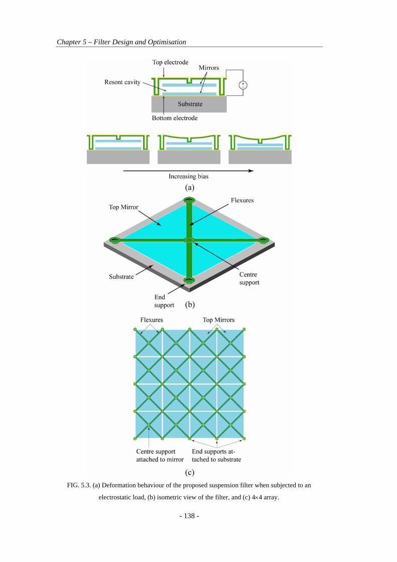
Chapter 5 – Filter Design and Optimisation
- 138 -
FIG. 5.3. (a) Deformation behaviour of the proposed suspension filter when subjected to an
electrostatic load, (b) isometric view of the filter, and (c) 4×4 array.

Chapter 5 – Filter Design and Optimisation
- 139 -
An isometric view of the proposed suspension filter is shown in Fig. 5.3(b). The
flexures consist of two fixed-fixed beams joined at the centre, where they attach to the top
mirror. The ends of the flexures are attached to the substrate via end supports. As the
flexures of the filter shown in Fig. 5.3(b) are positioned above the mirrors, the optically
active area is increased. Figure 5.3(c) shows a 4×4 array of filters. For this particular set
of filters, the mirror sizes are 100×100 µm, the flexure widths are 6 µm and the spacing
between adjacent mirrors is 4 µm. The resulting fill-factor is 79 %. The fill-factor can be
further increased by modifying the flexures such that they consist of only one fixed-fixed
beam. It is expected however that this flexure design will be less reliable when actuated
due to its susceptibility to torsion.
In comparison to the filters proposed by Huang et al. the suspension filter
combines the advantages of the four designs:
• Similar to designs (i), (ii) and (iii) in Fig. 5.1, the suspension filter utilises fixed-fixed
beams which are advantageous compared to cantilever beams due to larger
achievable displacements, and better displacement control of the top mirror at higher
actuation voltages.
• Similar to designs (i), (ii) and (iii) in Fig. 5.1, the mirror deformation of the
suspension filter is, in principle, independent of σ0 in the flexures provided the stress
is tensile or less than the Euler buckling limit if the stress is compressive.
• Similar to design (iv), the suspension filter design results in less mirror deformation
during actuation as the mirror is mechanically independent of the flexures.
The fill factors of the four designs proposed by Huang et al. however are inferior to the
new suspension filter. Designs (i), (ii) and (iii) in Fig. 5.1 have fill factors of
approximately 17%, whilst the fill factor of design (iv) is 25%.
As mentioned in Section 3.6, the displacement of a fixed-fixed beam when
subjected to an electrostatic force is typically around 40 % of the cavity length. A further
increase in the applied bias will result in pull-in of the beam onto the substrate. In the
suspension filter design, positioning the flexures above the top mirror increases the
electrostatic cavity size (i.e. the distance between the top and bottom electrodes).
Consequently, designing the filter so that the flexures are positioned above the top mirror
should, in principle, increase the displacement of the mirror before pull-in. This is a major

Chapter 5 – Filter Design and Optimisation
- 140 -
advantage compared to the four filter designs proposed by Huang et al. Larger mirror
displacements result in a larger achievable FSR. If a high degree of parallelism is
maintained across the suspension filter’s tuning range, smaller line widths of the resonant
peaks can be expected, resulting in higher cavity finesse.
5.3. Fabrication of the Proposed Suspension Filter
Fabrication of the new FP filter design was initially carried out to determine its
feasibility, as well as optimising the required process steps. Due to resolution limitations
of emulsion masks, the dimensions of the FP filter illustrated in Fig. 5.3 were scaled up.
The resolution required for the successful fabrication of the suspension filter however can
be easily achieved using Cr masks. For initial device fabrication, the bottom mirror and
the top and bottom electrodes were omitted from the fabrication steps, and a Si substrate
was used.
Figure 5.4 shows the steps used to fabricate single mirror filters on Si substrates.
The Si substrates were initially dipped in HF to remove the native oxide layer. Polyimide
(PI)-2616 was then spun onto the substrates and baked at 130 ºC for 20 minutes
(Fig. 5.4(a)). More information on partial curing of polyimides can be found in Ref. [10].
The spin speed versus film thickness curve of partially cured (130 ºC for 20 minutes)
PI-2616 is shown in Fig. 5.5. For the first polyimide layer, a spin speed of 3000 rpm was
used. The top mirrors were then deposited and defined using a dry etch process consisting
of CF4 plasma (Fig. 5.4(b)). The top mirrors were fabricated from e-beam evaporated
Ge/SiO/Ge stacks of thickness 120/280/120 nm, as proposed by Dell et al. and
Antoszewski et al. [1, 6]. The Ge and SiO layers were both deposited at 10 Å/s. The
mirror deposition was carried out using a BOC Edwards Auto 500 Vacuum Coater. This
system enables alternate layers of Ge and SiO thin films to be deposited for the one
pump-down process, thus minimising contamination of the layers.
Photo-definable PI-2737 was then spun on at 7000 rpm and baked initially at
100 ºC for 1 minute, followed by a second bake at 130 ºC for 1 minute (Fig. 5.4(c)). After
baking, the sample was flood exposed under a UV source for 40 s. This second PI layer
defines the spacing between top mirror and the flexures and acts as the second sacrificial
layer. PI-2616 cannot be used for this step as solvent transfer will occur between the two
PI layers, resulting in delamination of the patterned top mirrors. The spin speed versus

Chapter 5 – Filter Design and Optimisation
- 141 -
FIG. 5.4. Process steps necessary for the fabrication of a single mirror FP filters on Si.

Chapter 5 – Filter Design and Optimisation
- 142 -
film thickness curve of PI-2737 using this process is also shown in Fig. 5.5. The
polyimide layers were then patterned using a dry etch process consisting of 1:20 gas
mixture ratio of CH4:O2 (Fig. 5.4(d)). This step was carried out using a two mask process
– one mask to etch both polyimide layers down to the substrate (for the ends supports)
and another mask to etch the second polyimide layer down to the top mirror (for the
centre support). This method minimised etching times of the centre support etch and thus
reduced etching in directions parallel to the substrate. To improve step coverage, a
photoresist with an overcut profile was used (see Section 2.5).
The flexures were then deposited from β-series 500 nm thick PECVD SiNxHy thin
films deposited at 125 ºC (Fig. 5.4(e)). In Chapter 4, it was shown that films deposited
under these conditions contain only moderate residual tensile stresses, which are desirable
for producing flat filters. Etching of the flexures was then carried out using CF4 plasma.
The filters were then released from the polyimide sacrificial layers using a wet process
(Fig. 5.4(f)) consisting of a weak base (see Section 2.2). Samples were then washed in
deionised water and transferred to methanol to be dried using a critical point dryer (see
Section 2.5).
FIG. 5.5. Dependences of film thickness on spin speed for Polyimide (PI)-2616
and PI-2737.

Chapter 5 – Filter Design and Optimisation
- 143 -
Figure 5.6 shows optical images of arrays of FP filters (bottom mirror and
electrodes omitted) fabricated on Si wafers. Figure 5.6(a) and (b) shows unreleased filters
with double and single support flexures, respectively. Figure 5.6(c) and (d) shows the
filters after the sacrificial layers have been removed. The sizes of the top mirrors are
250×250 µm. It is obvious from Fig. 5.6(c) and (d) that the mirrors are not planar once
the sacrificial layers are removed. Figure 5.7 plots the height variation across the centre
of one of the released suspension filters. The height measurement was obtained using an
optical profilometer. The centre support is not plotted in the figure as it was out of focus
during the measurement. The plot show the mirror curves right down to the substrate. As
the mirrors are symmetrical through their thickness, the curvature can only be due to
stress gradients in the mirror materials (see Section 3.4).
It is well known that some physical vapour deposited (PVD) thin films exhibit
thickness-dependent stress distributions (i.e. stress gradients) [11, 12]. During a PVD
event, source material is boiled onto the substrate. Depending on the material, the
FIG. 5.6. Optical images of fabricated FP filters with double supports (a) and single supports
(b) in the unreleased state, and released state (c and d). The sizes of the mirrors are
approximately 250×250 µm.

Chapter 5 – Filter Design and Optimisation
- 144 -
evaporant can be many thousands of degrees in temperature, and consequently, the
temperature of the substrate will inevitably increase during deposition. Changes in
substrate temperature during deposition will lead to changes in grain size and growth
through the thickness of the film. The stress in PVD films is also dependent on the rate of
deposition. If the rate of deposition is too high, energy minimisation by atom diffusion
across the sample’s surface is restricted, resulting in a build-up of stress in the film. Mayr
et al. [11] showed as film thickness increases, the grain structure of e-beam evaporated
Zr65Al7.5Cu27.5 film and the surface roughness of the film increase. Guisbiers et al. [12]
showed the average tensile stress in e-beam deposited Ta, Al, Mo and Pd thin films
decreased with increasing film thickness, suggesting the existence of stress gradients.
Winchester [8] showed using a ray approach that even a small deviation (a few
nanometres) in parallelism between the top and the bottom mirrors will have detrimental
effects on the finesse and transmission of the cavity. Depending on its transmission, the
finesse of a cavity can be reduced by as much as an order of magnitude if deviations from
parallel exceed 10 nm [8]. Figures 5.6 and 5.7 clearly show the mirror system used is
unacceptable, and highlights the vulnerability of the suspension filter to stress gradients in
FIG. 5.7. Height variation across the top mirror of a released suspension filter
measured using an optical profilometer. The variation was measured across the
centre of a filter (see insert).

Chapter 5 – Filter Design and Optimisation
- 145 -
the top mirror. The stress gradients in the Ge/SiO/Ge mirror stack have less of an
influence towards cavity finesse for an X-style filter design [1, 6, 8, 13, 14]. In order to
remove the curvature in the top mirror of the suspension filter, three methods are
considered:
• Change the deposition conditions (deposition rate, substrate temperature etc.) to
change grain growth in Ge and SiO films.
• Deposit an additional thin film layer in the mirror stack to compensate for the stress
non-uniformity through the thickness of the mirrors.
• Use an alternative mirror stack system.
Deposition systems containing substrate temperature controllers can be utilised to change
the grain growth of a PVD film [15, 16]. Due to processing temperature constraints,
increasing the substrate temperature to improve the stress uniformity of the Ge and SiO
films is not feasible. A thermal evaporation system fitted with a substrate temperature
controller was utilised to evaporate Ge and SiO films whilst maintaining a constant
substrate temperature of 25 ºC. It was found however that this made little difference to the
stress gradients. Changing the deposition rates of the Ge and SiO thin films is another
alternative to improving stress gradients [17]. However, the optical performance of the
mirror stack is optimised at deposition rates of 10 Å/s [6].
Depositing an additional thin film layer is feasible, provided it does not affect the
optical properties of the filter. The material would need to be free of stress gradients
itself, or at least result in curvature of the mirror in the opposite direction (i.e. curve
mirror up instead of down). PECVD SiNxHy is an ideal choice as its stress profile can be
easily controlled with changes in process conditions. The film (deposited at temperatures
at, or below 125 ºC) would be deposited before or after the deposition of the Ge/SiO/Ge
stack. In order to flatten the mirror, a SiNxHy film deposited before the mirror deposition
event would need to be compressive in nature, or tensile if deposited after the mirror.
Using alternative mirror materials in the stack is also a feasible option. Due to its
excellent mechanical properties, low surface roughness [18] and high refractive index,
PECVD a-Si:H is an ideal choice for use as the high refractive index material in the top
mirror. Further, it has been shown that PECVD a-Si:H can be deposited at low
temperatures with zero stress gradient [19], allowing for highly parallel mirrors to be
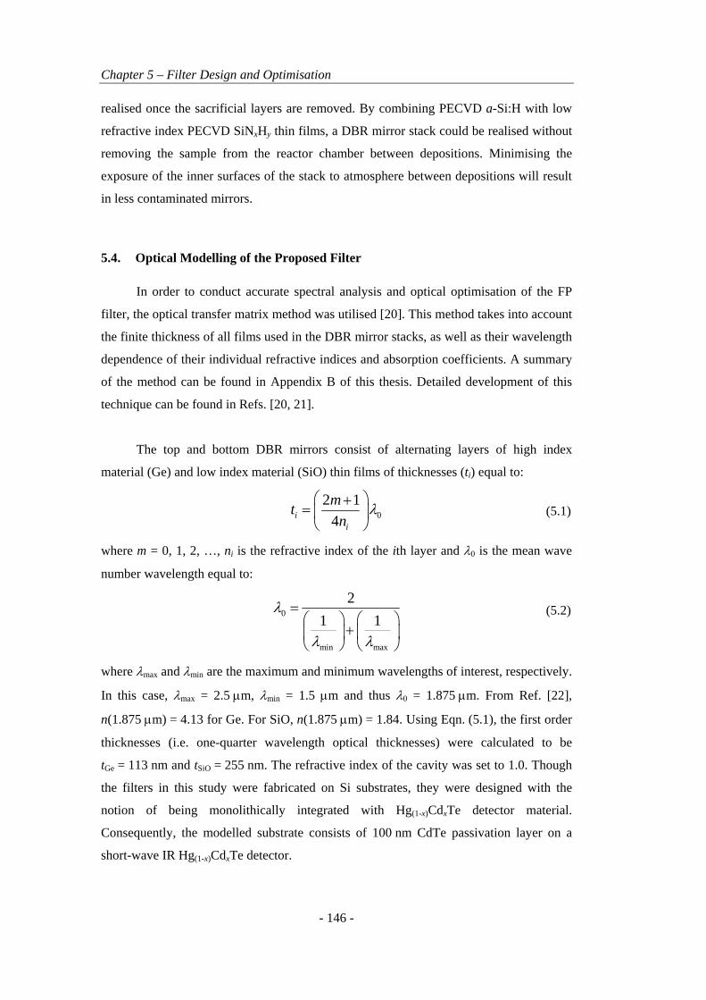
Chapter 5 – Filter Design and Optimisation
- 146 -
realised once the sacrificial layers are removed. By combining PECVD a-Si:H with low
refractive index PECVD SiNxHy thin films, a DBR mirror stack could be realised without
removing the sample from the reactor chamber between depositions. Minimising the
exposure of the inner surfaces of the stack to atmosphere between depositions will result
in less contaminated mirrors.
5.4. Optical Modelling of the Proposed Filter
In order to conduct accurate spectral analysis and optical optimisation of the FP
filter, the optical transfer matrix method was utilised [20]. This method takes into account
the finite thickness of all films used in the DBR mirror stacks, as well as their wavelength
dependence of their individual refractive indices and absorption coefficients. A summary
of the method can be found in Appendix B of this thesis. Detailed development of this
technique can be found in Refs. [20, 21].
The top and bottom DBR mirrors consist of alternating layers of high index
material (Ge) and low index material (SiO) thin films of thicknesses (ti) equal to:
02 1
4ii
mtn
λ⎛ ⎞+
= ⎜ ⎟⎝ ⎠
(5.1)
where m = 0, 1, 2, …, ni is the refractive index of the ith layer and λ0 is the mean wave
number wavelength equal to:
0
min max
21 1
λ
λ λ
=⎛ ⎞⎛ ⎞
+ ⎜ ⎟⎜ ⎟⎝ ⎠ ⎝ ⎠
(5.2)
where λmax and λmin are the maximum and minimum wavelengths of interest, respectively.
In this case, λmax = 2.5 µm, λmin = 1.5 µm and thus λ0 = 1.875 µm. From Ref. [22],
n(1.875 µm) = 4.13 for Ge. For SiO, n(1.875 µm) = 1.84. Using Eqn. (5.1), the first order
thicknesses (i.e. one-quarter wavelength optical thicknesses) were calculated to be
tGe = 113 nm and tSiO = 255 nm. The refractive index of the cavity was set to 1.0. Though
the filters in this study were fabricated on Si substrates, they were designed with the
notion of being monolithically integrated with Hg(1-x)CdxTe detector material.
Consequently, the modelled substrate consists of 100 nm CdTe passivation layer on a
short-wave IR Hg(1-x)CdxTe detector.

Chapter 5 – Filter Design and Optimisation
- 147 -
5.4.1. Transmission Spectrum of Stress-Free Mirrors
Figure 5.8 illustrates two different mirror stack designs and their corresponding
transmission spectrums. In the design shown in (a), the top mirror is of a three-layered
stack consisting of one-quarter wavelength thicknesses of Ge/SiO/Ge thin films. The
bottom mirror has an identical stack structure. In the design shown in (b), the top mirror
remains the same as in (a) but the bottom mirror contains an extra one-quarter wavelength
thick SiO layer below. The respective transmission spectrums of the two stacks are shown
in Fig. 5.8(c) and (d). To obtain these spectrums, the n and extinction coefficient (k)
values for each material were taken from Ref. [22] and the top mirrors are assumed
perfectly flat and free of stress gradients. The cavity lengths corresponding to each peak
are shown above the graphs. The FSR for each filter is similar (~1.5-2.5 µm), however
the transmission intensity and finesse of the cavity for the three-layered bottom mirror
stack are both lower compared to the four-layered bottom mirror stack. Table 5.1 lists the
FWHM and associated cavity finesse for each transmission peak shown in Fig. 5.8.
For a cavity size of 1400 nm, the first and second order resonant peaks occur at
wavelengths of 2502 nm and 1486 nm, respectively for the filter with the three-layered
bottom mirror, and 2486 nm and 1491 nm, respectively for filter with the four-layered
bottom mirror. This corresponds to FSR values for the three- and four-layered bottom
mirror filters equal to 1016 nm and 995 nm, respectively. Increasing the number of layers
of a mirror stack in a filter will increase the cavity finesse, whilst reducing its FSR [21].
The additional SiO layer in the bottom mirror increases the filter’s transmission due to
better matching of the top and bottom mirror with the inclusion of the substrate.
5.4.2. Inclusion of a Stress Compensating Film
As mentioned in Section 5.3, the inclusion of a SiNxHy layer in the top mirror stack
should aid in improving parallelism. SiNxHy thin films have a low refractive index
(n ≈ 1.8), and very low extinction coefficients [6]. Using nSiNxHy = 1.8, from Eqn. (5.1) the
one-quarter wavelength optical thickness of SiNxHy is 260 nm. Figure 5.9 plots the
theoretical transmission spectrums of filters on Hg(1-x)CdxTe substrates with the inclusion
of a SiNxHy layer positioned at the bottom of the top mirror. The bottom mirror is
identical to that shown in Fig. 5.8(b). Figure 5.9(b), (c) and (d) plot the transmission
spectrums of filters with SiNxHy optical thicknesses equal to one-quarter wavelength
(260 nm), one-eighth wavelength (130 nm) and one-sixteenth wavelength (65 nm),

Chapter 5 – Filter Design and Optimisation
- 148 -
FIG. 5.8. Optical impedance matrix modelling of two different FP filters, (a) and (b) illustrate
FP filters with a three and four-layered bottom mirrors, respectively, (c) and (d) show the
transmission spectrums of the filters shown in (a) and (b), respectively.
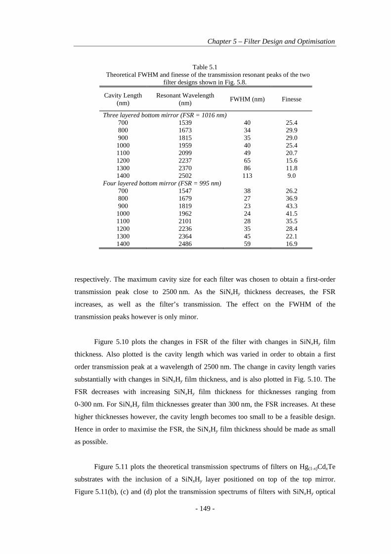
Chapter 5 – Filter Design and Optimisation
- 149 -
respectively. The maximum cavity size for each filter was chosen to obtain a first-order
transmission peak close to 2500 nm. As the SiNxHy thickness decreases, the FSR
increases, as well as the filter’s transmission. The effect on the FWHM of the
transmission peaks however is only minor.
Figure 5.10 plots the changes in FSR of the filter with changes in SiNxHy film
thickness. Also plotted is the cavity length which was varied in order to obtain a first
order transmission peak at a wavelength of 2500 nm. The change in cavity length varies
substantially with changes in SiNxHy film thickness, and is also plotted in Fig. 5.10. The
FSR decreases with increasing SiNxHy film thickness for thicknesses ranging from
0-300 nm. For SiNxHy film thicknesses greater than 300 nm, the FSR increases. At these
higher thicknesses however, the cavity length becomes too small to be a feasible design.
Hence in order to maximise the FSR, the SiNxHy film thickness should be made as small
as possible.
Figure 5.11 plots the theoretical transmission spectrums of filters on Hg(1-x)CdxTe
substrates with the inclusion of a SiNxHy layer positioned on top of the top mirror.
Figure 5.11(b), (c) and (d) plot the transmission spectrums of filters with SiNxHy optical
Table 5.1
Theoretical FWHM and finesse of the transmission resonant peaks of the two filter designs shown in Fig. 5.8.
Cavity Length (nm)
Resonant Wavelength (nm) FWHM (nm) Finesse
Three layered bottom mirror (FSR = 1016 nm) 700 1539 40 25.4 800 1673 34 29.9 900 1815 35 29.0 1000 1959 40 25.4 1100 2099 49 20.7 1200 2237 65 15.6 1300 2370 86 11.8 1400 2502 113 9.0
Four layered bottom mirror (FSR = 995 nm) 700 1547 38 26.2 800 1679 27 36.9 900 1819 23 43.3 1000 1962 24 41.5 1100 2101 28 35.5 1200 2236 35 28.4 1300 2364 45 22.1 1400 2486 59 16.9

Chapter 5 – Filter Design and Optimisation
- 150 -
FIG. 5.9. Theoretical transmission spectrums of an FP filter with a SiNxHy layer included at the
bottom of the top mirror, (a) illustrates the filter layers, and (b), (c) and (d) show the
transmission spectrums of the filter for SiNxHy thicknesses of 260 nm, 130 nm and 65 nm,
respectively.
Chapter 5 – Filter Design and Optimisation
- 151 -
thicknesses equal to one-quarter wavelength (260 nm), one-eighth wavelength (130 nm)
and one-sixteenth wavelength (65 nm), respectively. The plots show that as the thickness
of the SiNxHy layer increases, the FSR increases slightly, as well as the FWHM. Similar
to the filters shown in Fig. 5.9, the transmission of the filter in Fig. 5.11 improves with
decreasing SiNxHy thickness. The change in cavity length required to obtain a first order
transmission peak at 2500 nm is almost independent of changes in SiNxHy thickness. This
result alone shows the performance of the filter is less influenced by changes in SiNxHy
thickness, which is a desired result when tuning SiNxHy thicknesses to obtain flat mirrors.
5.4.3. Alternative Mirror Designs
Figure 5.12 plots the transmission spectrums of alternative mirror designs using
a-Si:H as the high refractive index material. At 1875 nm, the refractive index of a-Si:H is
3.44 [22]. From Eqn. (5.1), the one-quarter wavelength optical thickness of the a-Si:H
layer is 136 nm. Figure 5.12(a) and (b) shows a filter design and its respective
transmission spectrum consisting of a-Si:H and SiNxHy layers as the high and low
refractive index layers in the top mirror, respectively. The high transmission, high FSR
FIG. 5.10. FSR verses SiNxHy film thickness on the bottom of the top mirror. The cavity length
(also plotted) was varied so that the first order transmission peak occurred at a wavelength of
2500 nm.

Chapter 5 – Filter Design and Optimisation
- 152 -
FIG. 5.11. Theoretical transmission spectrums of an FP filter with a SiNxHy layer included at
the top of the top mirror, (a) illustrates the filter layers, and (b), (c) and (d) show the
transmission spectrums of the filter for SiNxHy thicknesses of 260 nm, 130 nm and 65 nm,
respectively.

Chapter 5 – Filter Design and Optimisation
- 153 -
FIG. 5.12. (a), (c) and (e) illustrate alternative FP filter designs utilising a-Si:H thin films, (b),
(d) and (e) plot their respective theoretical transmission spectrums.

Chapter 5 – Filter Design and Optimisation
- 154 -
and low FWHM suggest that this filter design would serve as a good replacement for the
previous filter design which incorporates Ge and SiO in the top mirror. Figure 5.12(c)
shows another alternative filter design which incorporates an air cavity in the top mirror
to replace the SiNxHy layer. The transmission spectrum for this filter design is shown in
Fig. 5.12(d). The air cavity in the top mirror is designed so that it has a fixed cavity length
equal to one-quarter wavelength optical thickness (equal to 469 nm using Eqn. (5.1)
assuming nair = 1.0). This filter design has improved line widths, as well as a higher FSR,
however the transmission is lower. Better matching of the top and bottom mirror is
achieved using the bottom mirror design shown in Fig. 5.12(e), with its associated
transmission spectrum shown in Fig. 5.12(f). In this case the bottom mirror consists of
alternating layers of Ge and SiNxHy. Due to its lower absorption properties, the SiO layers
have been replaced with SiNxHy layers. The six-layered bottom mirror results in much
smaller line widths (FWHM = 9 nm for transmission peak at 1961 nm), and consequently
much higher cavity finesse (Fc = 111 for transmission peak at 1961 nm).
Adopting air as the low refractive index material in a DBR mirror system has
previously been shown to improve a FP filter’s optical performance, in terms of reducing
line-widths and improving cavity finesse [23]. In order to fabricate such a top mirror, the
469 nm separation between the two a-Si:H layers would need to be defined using a
sacrificial layer. As shown in Fig. 5.13, incorporating this mirror design into the new
FIG. 5.13. Top Mirror design incorporating a-Si:H layers and a one-quarter wavelength optical
thick sacrificial layer (thicknesses have been increased by a factor 5 for viewing purposes
only). The end supports are known shown.
Chapter 5 – Filter Design and Optimisation
- 155 -
filter design would be achieved by connecting the two a-Si:H layers via an extra a-Si:H
support layer, which would run underneath the supporting flexures. This would help to
maintain parallelism between the two a-Si:H mirror layers whilst not affecting the fill-
factor.
5.5. Mirror Curvature Optimisation
Due to time constraints, the filter designs incorporating a-Si:H thin films were not
considered for the fabrication of the tunable shortwave IR filter. Though the cavity
finesse of the filter design shown in Fig. 5.12(e) is desirable, fabrication of low-
temperature a-Si:H thin films separated by a 469 nm sacrificial layer requires extensive
research. In this work, the use of stress compensation layers incorporating SiNxHy into the
Ge/SiO/Ge top mirror stack is studied. As discussed in Section 5.4.2, it is desirable to
control the stress in the top mirror by utilising a SiNxHy layer, deposited as thin as
possible, on top of the mirror stack (i.e. outside of the cavity). Surface micromachined
microcantilevers consisting of e-beam evaporated one-quarter wavelength optical
thickness Ge/SiO/Ge layers and PECVD SiNxHy layers were fabricated to determine the
optimum thickness of the SiNxHy layer required to flatten the structure.
Figure 5.14 illustrates the process steps used to fabricate multilayer
microcantilevers. Polyimide-2616 was initially spun onto Si substrates at 3000 rpm and
baked at 130 ºC for 20 minutes. Patterning of the polyimide was carried out using a dry
etch process as explained previously. E-beam evaporated Ge and SiO thin films were then
deposited, followed by the deposition of a SiNxHy layer of known deposition time. The
films were then patterned into microcantilevers of various dimensions using CF4 plasma.
The polyimide layer was then removed using a weak base, followed by rinsing. The
samples were dried using a critical point dryer. The curvature of the beams was measured
using an optical profilometer.
For Ge/SiO/Ge mirrors that curve downwards due to stress gradients, the top
SiNxHy layer needs to be tensile in nature in order to flatten the mirror. To cancel out the
stress gradient in the mirror with the thinnest possible SiNxHy film, it needs to be
deposited with the highest possible tensile stress. As presented in Chapter 4 (Fig. 4.18),
the highest tensile residual stressed SiNxHy film that can be integrated with Hg(1-x)CdxTe is
a β-series film deposited at 125 ºC. Figure 5.15 plots the inverse in radius of curvature (R)

Chapter 5 – Filter Design and Optimisation
- 156 -
FIG. 5.14. Process steps used to fabricate surface micromachined multilayer thin film
microcantilevers.

Chapter 5 – Filter Design and Optimisation
- 157 -
against changes in SiNxHy thickness for microcantilevers consisting of β-series films
deposited at 125 °C on the topside of Ge/SiO/Ge quarter wavelength stack layers. As seen
in the figure, the SiNxHy film thickness required to flatten the cantilever (1/R = 0) is large
(approaching 2 µm). From the optical analysis shown in Fig. 5.11, thick SiNxHy films
deposited on top of the top mirror have detrimental effects on the optical properties of the
filter. Also, depositing such a thick film using PECVD is not practical. Consequently, in
order to flatten the top mirror, a compressively stressed SiNxHy film deposited on the
underside of the Ge/SiO/Ge stack is required. As presented in Chapter 4 (Fig. 4.18), the
highest compressive residual stressed SiNxHy film that can be integrated with Hg(1-x)CdxTe
is an α-series film a deposited at 100 ºC. For the purposes of this work however, an
α-series film deposited at 125 ºC was used to compensate for the stress in the top mirror.
SiNxHy films deposited under these conditions are more chemically inert compared to
lower temperature deposited film when subjected to a base (see Fig. 4.2). This will occur
during the PI release process. Though it is expected the amount of etching of a low-
temperature deposited SiNxHy film subjected to this process will be minimal, the sensitive
nature of compensating for the top mirror curvature requires a high degree of SiNxHy film
FIG. 5.15. β-series SiNxHy thin film compensating layer thickness and deposition time versus
1/R for microcantilevers consisting of Ge/SiO/Ge/SiNxHy multilayer stacks (SiNxHy on top).

Chapter 5 – Filter Design and Optimisation
- 158 -
thickness uniformity of across the mirror’s surface. As the release process of the
suspension filter involves etching of the PI underneath the top mirror, the etching front
starts at the edges of the mirror and will finish underneath its centre. Any etching of the
SiNxHy film during this process will result in a non-uniform film thickness across the
width of the top mirror.
Figure 5.16 plots the inverse in radius of curvature (R) against changes in SiNxHy
thickness for microcantilevers consisting of α-series films deposited at 125 °C on the
topside of Ge/SiO/Ge quarter wavelength stack layers. The figure shows that the stress
gradients in the mirror materials can be compensated for by depositing an α-series SiNxHy
thin film of thickness approximately 100-140 nm. From Fig. 5.9, a SiNxHy film of this
thickness will have negligible effects on the FSR and finesse of the cavity. Figure 5.17
illustrates an array of released single arm suspension filters fabricated on Si substrates
with α-series SiNxHy thin films of thickness 130 nm used as the stress compensating
layers. From optical profilometry measurements, the mirrors are bending up ~20 nm
along the diagonal from the centre supports, corresponding to a curvature of
FIG. 5.16. α-series SiNxHy thin film compensating layer thickness and deposition time versus
1/R for microcantilevers consisting of SiNxHy/Ge/SiO/Ge multilayer stacks
(SiNxHy on bottom).

Chapter 5 – Filter Design and Optimisation
- 159 -
approximately 0.001 mm-1. Though not completely optimised, Fig. 5.17 shows that
adopting a compressively stressed film to the underside of an e-beam deposited
Ge/SiO/Ge mirror can greatly improve its flatness.
5.6. Finite Element Modelling
Finite element modelling (FEM) was carried out using the software package
CoventorWare version 2006.1 to determine the mechanical performance and resonance
behaviour of the suspension filter that utilises a 130 nm thick SiNxHy thin film
compensation layer deposited underneath the top mirror. The modelled filter is shown in
Fig 5.18(a). It consists of 100×100 µm mirrors and 6 µm wide flexures. Since the bottom
mirror is a stationary object, it is not included in the model. The top Ge layer of the
bottom mirror serves as the bottom electrode. Metal-induced crystallisation of Ge results
in an increase in its conductivity, which is desirable for its function as the electrode. The
crystallisation can be achieved by incorporating a monolayer of In [24]. The supporting
FIG. 5.17. Optical micrograph of an array of released single arm filters fabricated on Si
substrates with α-series SiNxHy thin films of thickness 130 nm used as the stress compensating
layer in the mirror. The size of the mirrors are 250×250 µm.

Chapter 5 – Filter Design and Optimisation
- 160 -
flexures consist of a 300 nm thick SiNxHy layer and a 30 nm Au layer deposited on top as
the top electrode. The Au layer covers the SiNxHy layer in a conformal manner and hence
has continuity into the centre support. Due to its tensile nature, the SiNxHy flexure layer
will consist of a β–series film deposited at 125 ºC. From the measurements presented in
Chapter 4, the average residual stress, density and Young’s modulus of this film are
10 MPa, 1.68 g/cm3 and 78 GPa, respectively. From Ref [25], E(Au) = 66 GPa and
ρ(Au) = 19.3 g/cm3. Work carried out by Gall et al. [26] has shown that the average
residual stress in evaporated Au thin films can be easily tuned to a zero via low-
temperature annealing. For the purpose of this work, the residual stress in the Au layer
was set to 0 MPa.
The top mirror was modelled as a single material so that the Young’s modulus,
density and Poisson’s ratio were equivalent to the four-layer SiNxHy/Ge/SiO/Ge stack.
FIG. 5.18. Finite element model of proposed filter showing (a) total modelled filter, and (b)
meshed quarter model. In both cases, the dimensions in the z-direction have been increased by
a factor of 5 for viewing purposes only.

Chapter 5 – Filter Design and Optimisation
- 161 -
From Chapter 4, E and ρ of an α-series SiNxHy thin film deposited at 125 ºC are equal to
104 GPa and 2.18 g/cm3, respectively. The thickness of the α-series SiNxHy stress
compensating layer was set to 130 nm. From Ref [10], E(Ge) = 102 GPa, E(SiO) =
90 GPa, ρ(Ge) = 5.35 g/cm3, ρ(SiO) = 2.13 g/cm3. The dielectric constant (ε0) of the
mirror was modelled such that its total capacitance was the equivalent to the actual mirror
stack for the same thickness. The dielectric constant of the SiNxHy layers was
approximated to be equivalent to the square of its refractive index. From Fig. 5.9, a
130 nm thick SiNxHy stress compensation layer is equivalent to an optical thickness of
(1/8)λ and thus a cavity length of ~1.3 µm is required to obtain a first order resonant peak
at 2.5 µm. The distance between the flexures and the mirror was set to 800 nm. From
Fig. 5.5, a PI-2737 layer spun on at 9000 rpm will achieve this thickness.
To minimise the effects of non-symmetrical meshing, only a quarter of the filter
was meshed and symmetry boundary conditions utilised. Figure 5.18(b) shows the
meshed quarter filter model. As the centre support is circular in shape, the mirror and
flexures were meshed with a 5 µm tetrahedral mesh. The bottom electrode was meshed
with a 5 µm, hexahedral mesh. The boundary conditions of the nodes at the end of the
flexure were set so that all displacements and rotations were set to zero. Figure 5.19 plots
the centre mirror displacement versus applied bias to the top electrode for the meshed
filter shown in Fig. 5.18, with and without the inclusion of residual stress in the SiNxHy
flexure layer. From the optical modelling shown in Fig. 5.9, the cavity length required to
obtain a first order resonant peak at 1502 nm is approximately 650 nm. To achieve this
cavity length, the top mirror needs to be displaced by ~750 nm, which is ~57% of the
initial cavity length. Figure 5.18 suggests that this displacement is easily achievable if the
residual stress in the flexures is zero, however it cannot be achieved without pull-in
occurring if the residual stress in the flexures is included. The tuning range of the mirror
can be increased by increasing the distance between the mirror and the flexures. This will
however increase the required actuation voltage, which is not feasible as the maximum
required voltage shown in Fig. 5.19 is already close to 30 V – the maximum allowable
voltage for the integration of this technology with application-specific integrated circuits
(ASICs) required for filter control and detector signal acquisition.
Milne et al. [27] has shown by varying the dimensions of a fixed-fixed beam, the
displacement of the beam can be increased before pull-in occurs. Figure 5.20 shows the
centre mirror displacement versus applied bias for the meshed filter shown in Fig. 5.18,
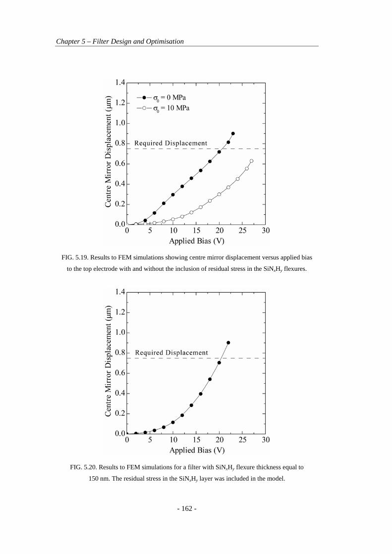
Chapter 5 – Filter Design and Optimisation
- 162 -
FIG. 5.19. Results to FEM simulations showing centre mirror displacement versus applied bias
to the top electrode with and without the inclusion of residual stress in the SiNxHy flexures.
FIG. 5.20. Results to FEM simulations for a filter with SiNxHy flexure thickness equal to
150 nm. The residual stress in the SiNxHy layer was included in the model.

Chapter 5 – Filter Design and Optimisation
- 163 -
except with the thickness of the SiNxHy flexure layer halved to 150 nm. A residual stress
of 10 MPa was included in the model for this layer. As seen in the figure, the required
displacement of 750 nm is easily achieved using this design, at an actuation bias voltage
just over 20 V. This is a desirable result.
An interesting feature of this filter design is the curling of the mirror towards the
flexures (top electrode) when a bias voltage is applied. As discussed in section 5.2, the
suspension filter is free of the problem of large mirror distortion during mirror
displacement driven by electrostatic force on the top electrode because of the separation
of the electrode and the mirror. However, a much minor attraction force may occur cross
the gap between the mirror and the top electrodes (the flexures) when a voltage is applied.
Under the influence of this force, the corners of the mirror situating just under the
flexures will curve up, causing mirror distortion. Modelling results suggest that the mirror
distortion is negligible. For example, under the influence of a 20 V bias voltage, the
corners of the mirror deflect only 5.1 nm towards the top electrode. This level of mirror
distortion is of the same order of magnitude as the surface roughness of evaporated SiO
and Ge thin films [10] and will have negligible effect on the finesse of the cavity.
A modal analysis was conducted on the filter designed with 150 nm thick SiNxHy
flexure supports to determine the frequencies the filter will resonate. Figure 5.21
illustrates the first three resonant modes and their associated frequencies. The first mode
occurs at 26.1 kHz and involves bending of the flexures. The second and third resonant
modes occur at much higher frequencies (199 kHz and 281 kHz) and involve bending in
the top mirror. Ideally, the filter needs to operate at a high frequency (~10 kHz). As the
vibration modes of the filter are much higher than 10 kHz, there will not be any
detrimental effects regarding filter resonance on the performance of the device.
5.7. Device Fabrication
Suspension filters were fabricated specifically for optical and electro-mechanical
testing. Figure 5.22 illustrates schematically the cross-sectional profile of a filter
fabricated on double-sided polished Si substrates. Emulsion masks were utilised, so in
order to obtain the desired resolution, large devices were fabricated. The devices were
fabricated with 200×200 µm mirrors as well as longer flexures. Thicker SiNxHy layers

Chapter 5 – Filter Design and Optimisation
- 164 -
FIG. 5.21. The first three resonant modes of the proposed filter with 150 nm thick SiNxHy
flexures. The residual stress in the SiNxHy flexure layer was included in the model.

Chapter 5 – Filter Design and Optimisation
- 165 -
(410 nm) were also employed for the flexures. An Au layer of 100 nm thickness was used
to act as a shield for the optical measurements (see section 5.8). Thick Au layers
(300 nm) were deposited on areas of the support arms where changes in step height
occurred and in areas where bonding pads were positioned. All Au depositions employed
a thin layer (5 nm) of Cr to improve Au adhesion. For these devices, the Si substrate
served as the bottom conductor. A detailed summary on the processing steps used to
fabricate such a device is presented in Appendix C of this thesis.
Figure 5.23 shows scanning electron microscopic (SEM) images of two filters,
which are poorly fabricated. Fig. 5.23(a) shows a filter with two fixed-fixed beam
supports for the top mirror. The top mirror has detached from its flexures. This is due to
poor adhesion between SiNxHy and Ge. This problem was eradicated by performing an
additional CF4 etch to remove the Ge layer in the area where the flexures attach to the top
mirror, allowing the SiNxHy layer in the flexures to be deposited directly onto the SiO
layer in the top mirror at the centre support. The adhesion of SiNxHy on SiO is far better
than that of SiNxHy on Ge. Figure 5.23(b) illustrates a single fixed-fixed beam filter. This
filter features residual PI-2737 left on the filter. This is due to the polyimide layer not
being properly etched during the release process. Though PI-2616 can be easily etched at
FIG. 5.22. Schematic illustration of a cross-sectional profile of the proposed filter fabricated on
Si for the purpose of optical and electro-mechanical measurements.

Chapter 5 – Filter Design and Optimisation
- 166 -
FIG. 5.23. Scanning electron micrographs of poorly fabricated filters showing (a) detached
mirror of a filter consisting of double arm fixed-fixed beam flexures, and (b) residual PI-2737
hanging from a filter consisting of a single arm fixed-fixed beam flexure. The size of the
mirrors are 200×200 µm.
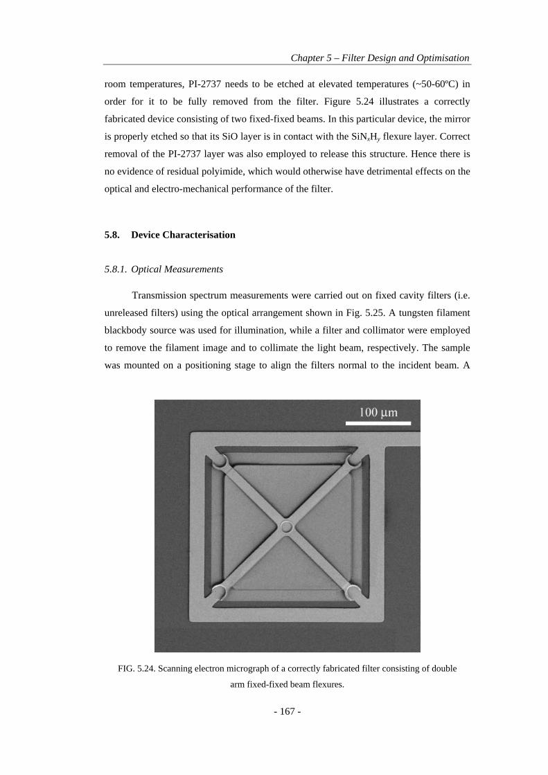
Chapter 5 – Filter Design and Optimisation
- 167 -
room temperatures, PI-2737 needs to be etched at elevated temperatures (~50-60ºC) in
order for it to be fully removed from the filter. Figure 5.24 illustrates a correctly
fabricated device consisting of two fixed-fixed beams. In this particular device, the mirror
is properly etched so that its SiO layer is in contact with the SiNxHy flexure layer. Correct
removal of the PI-2737 layer was also employed to release this structure. Hence there is
no evidence of residual polyimide, which would otherwise have detrimental effects on the
optical and electro-mechanical performance of the filter.
5.8. Device Characterisation
5.8.1. Optical Measurements
Transmission spectrum measurements were carried out on fixed cavity filters (i.e.
unreleased filters) using the optical arrangement shown in Fig. 5.25. A tungsten filament
blackbody source was used for illumination, while a filter and collimator were employed
to remove the filament image and to collimate the light beam, respectively. The sample
was mounted on a positioning stage to align the filters normal to the incident beam. A
FIG. 5.24. Scanning electron micrograph of a correctly fabricated filter consisting of double
arm fixed-fixed beam flexures.
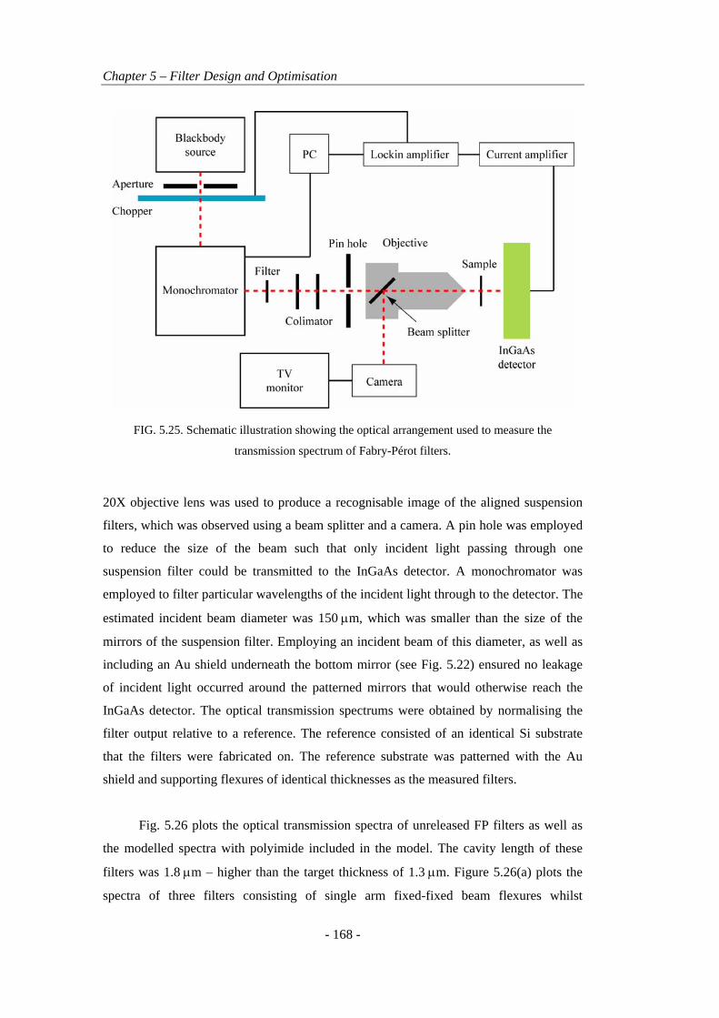
Chapter 5 – Filter Design and Optimisation
- 168 -
20X objective lens was used to produce a recognisable image of the aligned suspension
filters, which was observed using a beam splitter and a camera. A pin hole was employed
to reduce the size of the beam such that only incident light passing through one
suspension filter could be transmitted to the InGaAs detector. A monochromator was
employed to filter particular wavelengths of the incident light through to the detector. The
estimated incident beam diameter was 150 µm, which was smaller than the size of the
mirrors of the suspension filter. Employing an incident beam of this diameter, as well as
including an Au shield underneath the bottom mirror (see Fig. 5.22) ensured no leakage
of incident light occurred around the patterned mirrors that would otherwise reach the
InGaAs detector. The optical transmission spectrums were obtained by normalising the
filter output relative to a reference. The reference consisted of an identical Si substrate
that the filters were fabricated on. The reference substrate was patterned with the Au
shield and supporting flexures of identical thicknesses as the measured filters.
Fig. 5.26 plots the optical transmission spectra of unreleased FP filters as well as
the modelled spectra with polyimide included in the model. The cavity length of these
filters was 1.8 µm – higher than the target thickness of 1.3 µm. Figure 5.26(a) plots the
spectra of three filters consisting of single arm fixed-fixed beam flexures whilst
FIG. 5.25. Schematic illustration showing the optical arrangement used to measure the
transmission spectrum of Fabry-Pérot filters.

Chapter 5 – Filter Design and Optimisation
- 169 -
FIG. 5.26. (a) Modelled and measured optical transmission spectra of three FP filters
consisting of single arm fixed-fixed beam flexures, and (b) modelled and measured
transmission spectrum of three FP filters consisting of double arm fixed-fixed beam flexures.

Chapter 5 – Filter Design and Optimisation
- 170 -
Fig. 5.26(b) plots the spectra of three filters consisting of double arm fixed-fixed beam
flexures. The six filters were fabricated on the same Si wafer and spread across an area of
10×20 mm. The measured spectra of the filters show excellent agreement with the model
in terms of peak position. The measured transmissions of the peaks however are
approximately 20% lower compared to the modelled transmissions. This is most likely
due to the non-perfect nature of the mirrors in terms of surface roughness and parallelism
which the model does not take into account. The average line width of the peaks which
occur at ~2130 nm of the three measured filters plotted in Fig. 5.26(a) is 35 nm. A similar
average line width value of 36 nm is obtained for the filters plotted in Fig. 5.26(b). The
wavelength spread of the peaks which occur at ~2130 nm of the three measured filters
plotted in Fig. 5.26(a) is 10 nm, which is lower than the value of 25 nm obtained for the
filters in Fig. 5.26(b). The heights of the peaks in Fig. 5.26(a) are also slightly higher on
average, compared to the peaks in Fig. 5.26(b).
5.8.2. Electro-Mechanical Measurements
Figure 5.27 illustrates the deformation behaviour of the released FP filter shown in
Fig. 5.24 when subjected to an applied bias. The cavity length of this particular filter was
1.31 µm. Figure 5.27(a) plots height measurements of the filter along one of its support
arms when zero volts were applied to the top electrode. Also plotted are height
measurements of the filter once it had collapsed down to the substrate due to pull-in.
Measurements were obtained using an optical profilometer. These results show that under
zero applied bias, the flexure profile is flat across its length, except for its ends. The
unusual step at the beam’s right support is due to an optical profilometer error, which can
occur if there is a discontinuity in the data. Figure 5.27(b) plots the central mirror
displacement versus applied bias of the filter. Also plotted are simulated data obtained
from finite element modelling using the dimensions of the filter. The measured results
show excellent agreement with the model assuming the residual stress in the SiNxHy
flexure layer is 10 MPa, as obtained from stress measurement data in Chapter 4. The
mirror was displaced by applying a voltage across the top and bottom electrodes in steps
of 2.5 V. When 17.5 V was applied to the top electrode, the mirror displaced 620 nm. A
further increase in bias by 2.5 V resulted in pull-in, which lead to the top mirror being
permanently adhered to the bottom mirror and consequent failure of the device. The
simulation data however does suggest that if smaller voltage steps were used, stable
mirror displacements greater than 750 nm could be achieved.

Chapter 5 – Filter Design and Optimisation
- 171 -
FIG. 5.27. Results to the electro-mechanical measurements of the FP filter shown in Fig. 5.24.
(a) Height measurements of the filter along one of its support arms (see insert) when zero volts
was applied to the top electrode, as well as once the filter had collapsed due to pull-in.
Measurements were obtained using an optical profilometer. (b) Centre mirror displacement
versus applied bias of the filter shown in Fig 5.25. Also plotted are modelled results of the
filter for various residual stress values in the SiNxHy flexure layer.

Chapter 5 – Filter Design and Optimisation
- 172 -
5.9. Discussion
The optical measurements discussed in Section 5.8 suggest that FP filters
consisting of single arm fixed-fixed beam flexures perform slightly better optically
compared to FP filters consisting of double arm fixed-fixed beam flexures. This could be
due to dispersion which occurs due to the flexures being positioned directly above the
mirrors. As a double arm fixed-fixed beam flexure has a greater surface area compared to
a single arm fixed-fixed beam flexure, more dispersion will occur, thus having a
detrimental effect on the optical transmission spectra of the filter. Unfortunately no
spectra were measured on a released filter. The results presented above however do
suggest that the device design is feasible both optically and mechanically.
References
1. J. M. Dell, C. A. Musca, J. Antoszewski and L. Faraone, “Tunable Infrared Sensors – Integration of MEMS with Semiconductor Detectors,” IEEE/LEOS International Conference on Optical MEMS and Their Applications, p. 5-6 (2006).
2. M. A. Shah, V. Shanmugan, G. K. Chowdhury and R. Akkipeddi, “Optomechanical
design of tunable InP-based Fabry-Perot filters for wavelength division multiplexing applications,” Journal of Microlithography, Microfabrication and Microsystems, 4, p. 41303-1-8 (2005).
3. A. T. T. D. Tran, Y. H. Lo, Z. H. Zhu, D. Haronian and E. Mozdy, “Surface
micromachined Fabry-Perot Tunable Filter,” IEEE Photonics Technology Letters, 8, p. 393-395 (1996).
4. K. J. Winchester and J. M. Dell, “Tunable Fabry-Pérot cavities fabricated from
PECVD silicon nitride employing zinc sulphide as the sacrificial layer,” Journal of Micromechanics and Microengineering, 11, p. 589-594 (2001).
5. H. Huang, X. Z. Hu, M. B. Bush, K. J. Winchester, C. A. Musca, J. M. Dell and L.
Faraone, “Mechanical design and finite element analysis of tunable Fabry-Pérot MEMS structures for adaptive infrared detectors,” Conference on Optoelectronic and Microelectronic Materials and Devices (Brisbane, Queensland: IEEE), p. 205-208 (2004).
6. J. Antoszewski, K. J. Winchester, A. J. Keating, T. Nguyen, K. K. M. B. D. Silva,
C. A. Musca, J. M. Dell, L. Faraone, P. Mitra, J. D. Beck, M. R. Skokan and J. E. Robinson, “A monolithically integrated HgCdTe short-wavelength infrared photodetector and micro-electro-mechanical systems-based optical filter,” Journal of Electronic Materials, 34, p. 716-721 (2005).
7. V. Gogte and M. A. Matin, “MEM-Mirror design and analysis for tunable optical
filters,” Proceedings of SPIE, 5511, p. 199-206 (2004).

Chapter 5 – Filter Design and Optimisation
- 173 -
8. K. J. Winchester, Tunable Microelectromechanical Fabry-Perot Filters Using Plasma Enhanced Chemical Vapour Deposited Silicon Nitride Membranes, PhD Thesis, University of Western Australia (2003).
9. E. S. Hung and S. D. Senturia, “Extending the travel range of analog-tuned
electrostatic actuators,” Journal of Microelectromechanical Systems, 8, p. 497-505 (1999).
10. M. Martyniuk, Low-Temperature Micro-Opto-Electro-Mechanical Technologies for
Temperature Sensitive Substrates, PhD Thesis, University of Western Australia (2006).
11. S. G. Mayr and K. Samwer, “Model for intrinsic stress formation in amorphous thin
films,” Physical Review Letters, 87, p. 036105-1-4 (2001). 12. G. Guisbiers, S. Strehle and M. Wautelet, “Modeling of residual stresses in thin
films deposited by electron beam evaporation,” Microelectronic Engineering, 82, p. 665-669 (2005).
13. A. J. Keating, K. K. M. B. D. Silva, J. M. Dell, C. A. Musca and L. Faraone,
“Optical characterization of Fabry–Pérot MEMS filters integrated on tunable short-wave IR detectors,” IEEE Photonics Technology Letters, 18, p. 1079-1081 (2006).
14. C. A. Musca, J. Antoszewski, K. J.Winchester, A. J. Keating, T. Nguyen, K. K. M.
B. D. Silva, J. M. Dell, L. Faraone, P. Mitra, J. D. Beck, M. R. Skokan and J. E. Robinson, “Monolithic integration of an infrared photon detector with a MEMS-based tunable filter,” IEEE Electron Device Letters, 26, p. 888-890 (2005).
15. St. Bertel and R. Abermann, “Evolution of internal stress and microstructure in
Ti50Cu 50 alloy films: Influence of substrate temperature and composition,” Thin Solid Films, 473, p. 1-8 (2005).
16. C. Surgers, C. Strunk and H. Lohneysen, “Effect of substrate temperature on the
microstructure of thin niobium films,” Thin Solid Films, 239, p. 51-56 (1994). 17. S. Shao, Z. Fan, J. Shao, H. He, “Evolutions of residual stress and microstructure in
ZrO2 thin films deposited at different temperatures and rates,” Thin Solid Films, 445, p. 59-62 (2003).
18. G. T. Dalakos, J. L. Plawsky and P. D. Persans, “Surface roughness and structural
aspects of anodic and cathodic plasma deposited a-Si:H at low temperature,” Journal of Non-Crystalline Solids, 349, p. 285-290 (2004).
19. P. Danesh and B. Pantchev, “Mechanical stress in thin a-Si:H films,”
Semiconductor Science and Technology, 15, p. 971-974 (2000). 20. M. Born and E. Wolf, Principles of Optics 6th ed., Cambridge University Press,
Cambridge (1997). 21. H. A. Macleod, Thin-Film Optical Filters 3rd ed., Institute of Physics Publishing,
Bristol (2001).
Chapter 5 – Filter Design and Optimisation
- 174 -
22. D. Palik, Handbook of Optical Constants of Solids, Academic Press, Orlando (1985).
23. M. Datta, M. W. Pruessner, D. P. Kelly and R. Ghodssi, “Design of MEMS-tunable
novel monolithic optical filters in InP with horizontal Bragg mirrors,” Solid-State Electronics, 48, p. 1959-1963 (2004).
24. B. Dwir and G. Deutscher, “Structure and electrical properties of indium-
germanium interfaces,” Physical Review, B40, p.11880-11892 (1989). 25. B. Haung and T.-Y. Zhang, “Microbridge tests: II. On buckled thin gold films,”
Journal of Micromechanics and Microengineering, 16, p. 134-142 (2006). 26. K. Gall, N. West, K. Spark, M. L. Dunn and D. S. Finch, “Creep of thin film Au on
bimaterial Au/Si microcantilevers,” Acta Materialia, 52, p. 2133-2146 (2004). 27. J. Milne, J. Dell, A. Keating and L. Faraone, “Extended tuning range Fabry-Perot
etalon with doubly-supported beam actuators,” IEEE/LEOS Optical MEMS and Their Applications Conference, p. 134-135 (2006).

Chapter 6 – Conclusions and Future Work
- 175 -
Chapter 6
Conclusions and Future Work
6.1. Conclusions
This study has investigated the mechanical and physical properties of low-
temperature plasma enhanced chemical vapour deposited (PECVD) silicon nitride
(SiNxHy) thin films for the fabrication of short-wave infrared tunable Fabry-Pérot (FP)
filters with high fill factor, high cavity finesse and low actuation voltages. It has been the
intension of this work to fabricate a tunable filter that can be monolithically integrated
with Hg(1-x)CdxTe photoconductors and photodiodes. The main outcomes of this work are
in three groups: (1) development and verification of micromechanical testing techniques
of thin film materials, (2) determination and characterisation of mechanical and physical
properties of PECVD SiNxHy thin films, and (3) design and fabrication of the suspension
FP filter.
6.1.1. Development and Verification of Micromechanical Testing Techniques of
Thin Film Materials
A range of methods have been used to determine the Young’s modulus (E),
Poisson’s ratio (ν) residual stress (σ0) and density (ρ) of thin film materials. These
techniques include nanoindentation, microcantilever beam resonance method, the
microcantilever beam bending method, the micromembrane bulge test, and the quartz
crystal microbalance method.
(i) Nanoindentation, the resonance method, the microcantilever beam bending method
and the bulge test were used to determine the E of PECVD SiNxHy thin films. All

Chapter 6 – Conclusions and Future Work
- 176 -
methods have shown very good agreement to within 10% of the nanoindentation
method.
(ii) This study has shown the dependence of the resonance method on the dimensions
of resonating microcantilever beams and quantified the accuracy of standard
bending and torsional resonance equations using finite element modelling (FEM).
For microcantilever beams with length-to-width ratios greater than 8, the
resonance method used in this study to determine ν is accurate to within 7%.
(iii) The resonance method has also been used to determine ρ of thin film materials.
This method has shown very good agreement (to within 10%) of the quartz crystal
microbalance method.
(iv) This study has also derived an equation (Eqn. 4.12) which can be used to
determine E of microcantilever beams of variable thickness along their lengths
using the microcantilever beam bending method. This equation is necessary for
determining E from tapered beams caused by chemical microfabrication processes.
(v) The standard bulge test has been modified in this study to determine ν of thin
films. The modified bulge test varies from the standard bulge test in that both
square and rectangular-shaped membranes are fabricated alongside, and their
relative deflections are measured when subjected to an applied pressure. This new
invention allows for a more accurate determination of ν as the measurement is less
affected by variations in membrane dimensions. It has been shown that this method
closely agrees (to within 5%) with the resonance method used to determine ν.
(vi) The bulge test has also been used to determine σ0 of thin films. It has been shown
in this study that this method provided similar residual stress values compared to
the substrate curvature method, which was also utilised in this study.
6.1.2. Mechanical and Physical Properties of PECVD SiNxHy Thin Films
The Young’s modulus, Poisson’s ratio, residual stress and density of PECVD
SiNxHy thin films have been determined using the methods outlined above. In this study,
all PECVD SiNxHy thin films were deposited using an Oxford Instruments PECVD 80
system at an RF frequency of 13.6 MHz with SiH4:NH3:N2 flow rates of 5:50:100 SCCM.

Chapter 6 – Conclusions and Future Work
- 177 -
The deposition temperature varied between 100-300 ºC. The effects of changes of other
processing parameters such as chamber pressure and RF power on E, ν, σ0 and ρ have also
been evaluated.
(i) The highest E measured was 195 GPa for a film deposited at 300 °C, 600 mTorr
and 100 W. The lowest E measured was 54 GPa for a film deposited at 100 °C,
875 mTorr and 75 W. An increase in chuck temperature, increase in RF power and
decrease in chamber pressure all increase E.
(ii) The highest ρ measured was 2.90 g/cm3 for SiNxHy films deposited at 300 °C,
600 mTorr and 100 W. The lowest ρ measured was 1.55 g/cm3 for a SiNxHy film
deposited at 100 °C, 875 mTorr and 75 W. Increasing chuck temperature,
increasing RF power and decreasing chamber pressure all increase ρ, similar to the
case of E.
(iii) The highest ν value measured was 0.26 ± 0.01 for SiNxHy films deposited at
250 °C, 600 mTorr and 100 W. The lowest ν value achieved was 0.20 ± 0.01 for
SiNxHy films deposited at 100 °C, 875 mTorr and 75 W. An increase in chuck
temperature increases ν. Changes in RF power and chamber pressure have
negligible effect on ν.
(iv) The highest compressive residual stress measured was 133 MPa for SiNxHy films
deposited at 100 °C, 600 mTorr and 100 W. The highest tensile residual stress
achieved was 59 MPa for SiNxHy films deposited at 150 °C, 875 mTorr and 75 W.
Increasing the chuck temperature, decreasing the RF power and increasing the
chamber pressure all increase the tensile nature of the SiNxHy thin films.
6.1.3. Design and Fabrication of the Suspension FP Filter
This study has conducted the theoretical design, analysis and fabrication of a new
surface micro-machined short-wave infrared tunable Fabry-Pérot filter for adaptive
infrared photon detectors.
(i) A new concept support-membrane configuration for Fabry-Pérot filter design is
proposed. This design, termed the suspension filter, separates the top mirror from
the supporting flexures which allows for improved fill-factors (up to 79%), as well

Chapter 6 – Conclusions and Future Work
- 178 -
as increased tuning range. In order to improve parallelism of the filter, a PECVD
SiNxHy stress compensation layer was employed in the top mirror stack.
(ii) The suspension filter uses broad spectral range, high reflectivity distributed Bragg
reflector (DBR) mirrors, which results in very high finesse filters. It has been
shown a theoretical free spectral range (FRS) of approximately 1 µm (tuning
across wavelengths from 1.5 µm to 2.5 µm) is achievable using filters which
incorporate thermally evaporated Ge and SiO as the high and low-refractive index
materials in the DBR mirrors, respectively. A cavity finesse of more than 40 can
be achieved using this mirror system. An alternative mirror stack is also presented,
which incorporates a-Si:H and air as the high and low-refractive index materials in
the top mirror, respectively. This mirror system can theoretically achieve a similar
FSR as the Ge and SiO mirrors, however with an achievable cavity finesse of more
than 110.
(iii) Finite element modelling of the suspension filter has demonstrated top mirror
displacements of more than 900 nm (~64% of the cavity length) are achievable
with actuation voltages less than 30 V. As the required displacement for the filter
to tune across wavelengths from 1.5-2.5 µm is only 750 nm, it has been shown the
suspension filter can easily tune across this wavelength range. It has also been
shown the filter is able to maintain high cavity finesse during tuning, showing
negligible top mirror deformation across the desired wavelength range.
(iv) The fabrication process of this new design has also been established and arrays of
suspension filters, as well as a filter that could be actuated were successfully
fabricated. The filters were fabricated using a multiple sacrificial layer process to
define the resonant cavity spacer and the separation of the top mirror from the
supporting flexures. The flexures were fabricated from low-temperature (PECVD)
SiNxHy thin films.
(v) Optical characterisation of fabricated fixed cavity suspension filters on Si
substrates has shown transmissions of ~60% with small line widths (35 nm) are
achievable using the proposed mirror system incorporating Ge and SiO as the high
and low refractive index materials, respectively.
Chapter 6 – Conclusions and Future Work
- 179 -
(vi) A mirror displacement versus an applied bias voltage curve was obtained from a
released suspension filter fabricated on Si. A mirror displacement of 620 nm was
achieved whilst theoretical results suggest the required 750 nm mirror
displacement was possible if smaller voltage increments were used.
6.2. Future Work
It was the intention of this work to obtain transmission spectra of a released Fabry-
Pérot filter that could be tuned to a desired wavelength in the range 1.5-2.5 µm. This
work has shown that such a target is feasible and that more work in this area is worth
considering. The main challenges in realising this concept to a final engineering product
are:
• Improve device yield through better fabrication processes;
• Improving the optical performance of the filter;
• Gaining a better understanding of the dynamics of the suspension filter.
Recommended future work for research includes:
(i) More robust designs should be made possible using smaller mirror sizes, which
would require the use of Cr masks. Much higher resolutions are achievable using
Cr masks compared to emulsions masks, which were used in this study. Increasing
the resolution of the masks will enable smaller features to be fabricated, including
the size of the mirrors. Smaller mirror sizes will decrease their sensitivity to stress
gradients that exist in the mirror materials. High resolution masks will also help to
decrease errors associated with mask alignment and consequently result in better
performing devices both optically and mechanically, as well as increasing device
yield.
(ii) This work has also presented new mirror structure designs that utilise a-Si:H thin
films. Future work that focuses on optimising a-Si:H thin film processes could
prove useful in terms of improving cavity finesse and parallelism of the filter.
(iii) The dynamics of the suspension filter when actuated at high frequencies has not
been considered in this work. For hyperspectral imaging capabilities to be realised
using this technology, the filter would be required to move across the spectral

Chapter 6 – Conclusions and Future Work
- 180 -
tuning range in increments. At each increment, the filter would have a fixed
voltage applied between its electrodes for a finite period of time, whereby a
measurement would be taken. The time required for a measurement at each
increment is dependent on computation time as well as device settling time. It is
expected that the settling time of the proposed filter will be higher compared to
designs previously fabricated by researchers. It is the opinion of the writer that a
highly damped environment would be required to minimise the settling time
however, issues regarding squeeze-film damping need to be considered.

Appendix A –List of Symbols
- 181 -
Appendix A
List of Symbols σ Stress R Radius of curvature σ0 Residual stress ε0 Permittivity of free space F Force k Spring constant A Area V Voltage ε Strain ωn Angular frequency L Length λm Mean free path E Young’s modulus Mf Mass of deposited film ν Poisson’s ratio Mq Mass of quartz crystal τ Shear stress Fq Quartz crystal resonance G Shear modulus S Contact stiffness E’ Biaxial modulus Er Reduced modulus E* Plate modulus Fc Finesse of cavity γ Shear strain n Refractive index κ Curvature k Extinction coefficient w Deflection λ0 Mean wave number b Beam width N Complex refractive index t Beam thickness δ Phase shift of a wave z Distance η Admittance of a film M Bending moment Y Optical admittance I Moment of inertia E Electric field m Gradient of beam thickness H Magnetic field P Pressure R Reflectance
as,r Half width of a square/rectangle T Transmittance br Half length of rectangular A Absorbance

Appendix B –Deflection of a Tapered Beam due to a Point Load
- 182 -
Appendix B
Deflection of a Tapered Beam due to a
Point Load
This section derives the equation found in Chapter 3 on page 64 which describes
the deflection of a tapered beam due to a point load. Referring to Fig. B1, let tt be the
thickness of the beam at the point where the load F is applied and m be the gradient of the
beam thickness. Also, let L and b be the length and width of the beam, respectively. The
moment of inertia of the beam can thus be described using:
3( )12 tbI t mx= + (B.1)
From Eqn. (3.24):
2 * 2
*2 2 312 ( )t
d w E b d w xE I M Fxdx F dx t mx
= = ⇒ =+
(B.2)
Integrating with respect to x yields:
*
12 2
212 2 ( )
t
t
t mxE b dw CF dx m t mx
+= − +
+ (B.3)
FIG. B1. Tapered microcantilever beam due to bulk micromachining processes.
Appendix B –Deflection of a Tapered Beam due to a Point Load
- 183 -
( ) 1 2 2
202 ( )
t
t
t mLdw L Cdx m t mL
+= ⇒ =
+ (B.4)
Thus:
*
2 2 2 2
2 212 2 ( ) 2 ( )
t t
t t
t mx t mLE b dwF dx m t mx m t mL
+ += − +
+ + (B.5)
Integrating with respect to x yields:
*
23 3 2 2
( 2 )1 ln( )12 2 ( ) ( ) 2 ( )
t t tt
t t t
t t t mL xE bw t mx CF m t mx m t mx m t mL
⎡ ⎤ += − + + + +⎢ ⎥+ + +⎣ ⎦
(B.6)
( ) 2 3 3 2 2
( 2 )10 ln( )2 ( ) ( ) 2 ( )
t t tt
t t t
t t t mL Lw L C t mLm t mL m t mL m t mL
⎡ ⎤ += ⇒ = − + + + −⎢ ⎥+ + +⎣ ⎦
(B.7) Maximum deflection occurs at F, i.e. when x= 0. Hence:
[ ]*
3 3 3 3 2 2
( 2 )1 1 11 ln( ) ln( )12 2 2 ( ) ( ) 2 ( )
t t tt t
t t t
t t t mL LE bw t t mLF m m m t mL m t mL m t mL
⎡ ⎤ += − + − + + + −⎢ ⎥+ + +⎣ ⎦
(B.8) Rearranging yields:
* 3 2
(3 2 )6 2 ln(1 )( )
t
t t
mL mL tF mLwE bm t t mL
⎛ ⎞+⎛ ⎞⎛ ⎞= + −⎜ ⎟⎜ ⎟⎜ ⎟ +⎝ ⎠⎝ ⎠⎝ ⎠ (B.9)

Appendix C – Summary of the Optical Transfer Matrix Method
- 184 -
Appendix C
Summary of the Optical Transfer
Matrix Method
This section provides a brief summary on the basic theory required to calculate the
properties of multilayer thin film coatings. An introduction into the methods behind
calculating the reflectance of a single layer thin film on a substrate, as well as a multilayer
thin film assembly, is presented. More detail on these topics can be found in references
[1-4] found at the end of this Appendix.
C.1. The Reflectance of a Thin Film Covering a Substrate
This section outlines the equations used to determine the reflectance of an incident
plane wave normal to a single thin film covering a substrate. The film is said to be ‘thin’
FIG. C.1. Incident plane wave normal to a thin film on a substrate.

Appendix C – Summary of the Optical Transfer Matrix Method
- 185 -
when its thickness is less than the coherence length of the incident light. Figure C1
illustrates the arrangement of a plane wave, incident on a thin film. The film’s complex
refractive index (N1), can be described using the following:
111 iknN −= (C.1)
where n1 is the real part of the refractive index of the film, and k1 is known as the
extinction coefficient.
For a plane wave of normal incidence on a thin film covering a substrate, the sum
of the incident electric field and the reflected electric field (denoted Ea), and the sum of
the incident magnetic field and the reflected magnetic field (denoted Ha) are related to the
transmitted electric and magnetic fields (denoted Eb and Hb, respectively) via the optical
transfer matrix:
⎥⎦
⎤⎢⎣
⎡⎥⎦
⎤⎢⎣
⎡=⎥
⎦
⎤⎢⎣
⎡
b
b
a
a
HEi
iHE
δηδ
δηδ
cos/)sin(
sincos 1
1
(C.2)
where δ is equal to the phase shift of the wave and η1 is the admittance of the film. For a
plane wave of normal incidence:
y11 N=η (C.3)
where y is usually complex. In free space however, y is equal to 2.6544×10⁻³ S. The 2×2
matrix on the right side of Eqn. (C.2) is known as the characteristic matrix of the film.
The phase shift of a normal incidence plane wave travelling through the film’s thickness,
d is given by:
λπδ dN12
= (C.4)
where N1 is the complex refractive index of the film, and λ is the wavelength. Define the
input optical admittance, Y as:
a
a
EHY = (C.5)
The reflectance of an interface between an incident medium of admittance η0 and a
medium of admittance Y is equal to:
∗
⎟⎟⎠
⎞⎜⎜⎝
⎛+−
⎟⎟⎠
⎞⎜⎜⎝
⎛+−
=YY
YYR
0
0
0
0
ηη
ηη
(C.6)
Equation (C.2) can be normalised by dividing through by Eb:
⎥⎦
⎤⎢⎣
⎡⎥⎦
⎤⎢⎣
⎡=⎥
⎦
⎤⎢⎣
⎡=⎥
⎦
⎤⎢⎣
⎡
2
1
1
1cos
/)sin(sin
cos//
ηδηδ
δηδ i
iCB
EHEE
ba
ba (C.7)

Appendix C – Summary of the Optical Transfer Matrix Method
- 186 -
where
⎥⎦
⎤⎢⎣
⎡CB
(C.8)
is known as the characteristic matrix of the assembly. B and C represent the normalised
electric and magnetic fields at the front interface. From Eqns. (C.5) and (C.7), we can
write:
δηηδδηδη
sin)/(cossincos
12
12
ii
BC
EHY
a
a
++
=== (C.9)
Hence from Eqns. (C.6) and (C.9), the reflectance can be calculated.
C.2. The Reflectance of Multiple Thin Films Covering a Substrate
Consider the thin film setup shown in Fig. C.2. The characteristic matrix of the
film nearest the substrate is:
⎥⎦
⎤⎢⎣
⎡
2
22
22
2
cos
/)sin(sin
cosδ
ηδδη
δ ii
(C.10)
and
⎥⎦
⎤⎢⎣
⎡⎥⎦
⎤⎢⎣
⎡=⎥
⎦
⎤⎢⎣
⎡
c
c
b
b
HEi
iHE
2
22
22
2
cos/)sin(
sincos
δηδ
δηδ
(C.11)
Applying Eqn. (C.2), Ea and Ha can be calculated using:
FIG. C.2. Incident plane wave normal to two thin films on a substrate.

Appendix C – Summary of the Optical Transfer Matrix Method
- 187 -
⎥⎦
⎤⎢⎣
⎡⎥⎦
⎤⎢⎣
⎡⎥⎦
⎤⎢⎣
⎡=⎥
⎦
⎤⎢⎣
⎡
c
c
a
a
HEi
ii
iHE
2
22
22
2
1
11
11
1
cos/)sin(
sincos
cos/)sin(
sincos
δηδ
δηδ
δηδ
δηδ
(C.12)
and the characteristic matrix of the assembly is:
⎥⎦
⎤⎢⎣
⎡⎥⎦
⎤⎢⎣
⎡⎥⎦
⎤⎢⎣
⎡=⎥
⎦
⎤⎢⎣
⎡
32
22
22
2
1
11
11
1 1cos
/)sin(sin
coscos
/)sin(sin
cosηδ
ηδδη
δδ
ηδδη
δ ii
iiC
B (C.13)
Y is defined as before (C/B), and the reflectance is calculated using Eqn. (C.6). Hence, for
an assembly with q number of layers, the characteristic matrix is equal to the product of
the individual matrices:
⎥⎦
⎤⎢⎣
⎡
⎭⎬⎫
⎩⎨⎧
⎥⎦
⎤⎢⎣
⎡=⎥
⎦
⎤⎢⎣
⎡ ∏= m
q
r r
rr
rr
r iiC
Bηδ
ηδδη
δ 1cos
/)sin(sin
cos
1
(C.14)
where δr = 2πNrdr/λ and ηm is the optical admittance of the substrate.
C.3. Calculating the Transmittance and Absorbance of a Thin Film
Assembly
The transmittance of a thin film assembly is equal to the ratio of the net irradiance
at the exit side of the assembly (denoted the kth interface) to the net incidence irradiance:
)Re(
)1)(Re(∗
−==
BCR
II
T m
i
k η (C.15)
The transmittance is related to the assembly’s reflectance (R) and absorbance (A) via the
following equation:
1=++ TRA (C.16)
Substituting Eqn. (C.15) into (C.16) yields:
⎟⎟⎠
⎞⎜⎜⎝
⎛−−= ∗ )Re(
)Re(1)1(
BCRA mη (C.17)
Rewriting the reflectance in terms of B and C, Eqn. (C.6) can be written as:
∗
⎟⎟⎠
⎞⎜⎜⎝
⎛+−
⎟⎟⎠
⎞⎜⎜⎝
⎛+−
=CBCB
CBCB
R0
0
0
0
ηη
ηη
(C.18)
Inserting Eqn. (C.18) into Eqns. (C.15) and (C.17) yields:
∗++=
))(()Re(4
00
0
CBCBT m
ηηηη
(C.19)
Appendix C – Summary of the Optical Transfer Matrix Method
- 188 -
∗
∗
++−
=))(()Re(4
00
0
CBCBBC
A m
ηηηη
(C.20)
C.4. Concluding Remarks
From the above analysis, the transmittance, absorbance and reflectance of either a
singular thin film or a multilayer assembly are calculated directly from the complex
refractive index (Ni) and the thickness (di) of the films, as well as the substrate in which
the films are deposited on. It is also important to note that Ni is a function of λ. Values for
n and k used in this study were found in ref. [5].
References
1. H. A. Macleod, Thin-Film Optical Filters 3rd ed., Institute of Physics Publishing, Bristol (2001).
2. M. Born and E. Wolf, Principles of Optics 6th ed., Cambridge University Press,
Cambridge (1997). 3. O. S. Heavens, Optical Properties of Thin Solid Films, Dover Publications, New
York (1991). 4. K. J. Winchester, Tunable Microelectromechanical Fabry-Perot Filters Using
Plasma Enhanced Chemical Vapour Deposited Silicon Nitride Membranes, PhD Thesis, University of Western Australia (2003).
5. D. Palik, Handbook of Optical Constants of Solids, Academic Press, Orlando
(1985).

Appendix D – Device Processing Summary
- 189 -
Appendix D
Device Processing Summary
This section summarises the process steps necessary for the fabrication of the
tunable filter on Si substrates described in Section 5.7.
D.1. Si Wafer Clean
Step Step Details Piranha etch 1:1 H2SO4:H2O2
Immerse wafer once H2O2 is added to H2SO4 for 10 min Soak in hot trichloroethylene 50 °C for 5 min Soak in hot acetone 50 °C for 5 min Soak in hot methanol 50 °C for 5 min Soak in hot isopropanol 50 °C for 5 min Blow dry N2
D.2. Bottom Electrode Deposition
Step Step Details Dehydration 110 °C for 1 min Spin AZ 2035 resist 3000 rpm for 40 s Bake 110 °C for 1 min Mask 1 exposure 20 s exposure on Karl Suss mask aligner Bake 110 °C for 1 min Develop AZ 300 MIF 90 s, undiluted Rinse and blow dry N2 Load sample in thermal evaporator Evacuate <2×10⁻⁶ mBar Evaporate 50/1000 Å Cr/Au 1 Å/s for Cr, 10 Å/s for Au Cool down, remove from chamber Lift-off Soak in undiluted acetone Solvent rinse Soak in acetone, methanol and isopropanol Blow dry N2

Appendix D – Device Processing Summary
- 190 -
D.3. Bottom Mirror Deposition
Step Step Details Dehydration 110 °C for 1 min Load sample in E-beam Evacuate <2×10⁻⁶ mBar Evaporate 255/113/255/113 Å SiO/Ge/SiO/Ge
10 Å/s for all materials
Cool down, remove from chamber
D.4. Bottom Mirror Etch for Bottom Electrode Contact
Step Step Details Dehydration 110 °C for 1 min Spin 4562 resist 4000 rpm for 40 s Bake 100 °C for 90 s Mask 2 exposure 40 s exposure on Karl Suss mask aligner Develop 400 K 60 s, dilute with H20 1:3 Rinse and Blow dry N2 Load sample in Plasmalab 100 RIE CF4 10 sccm, 10 mTorr, 20 °C, 50/50 W RF/ICP, 30 min Remove resist in acetone Solvent clean Soak in acetone, methanol and isopropanol Blow dry N2
D.5. First Sacrificial Layer Deposition
Step Step Details Dehydration 130 °C for 1 min Spin Polyimide 2616 6000 rpm for 40 s Bake 130 °C for 20 min
D.6. SiNxHy Compensating Layer Deposition
Step Step Details Deposit SiNxHy using Oxford Instruments PECVD 80 System
Evacuate chamber for 15 min Deposit at 125 °C SiH4:NH3:N2 flow ratios 5:50:100 sccm 600 mTorr 100 W RF 4 min, 35 sec
D.7. Top Mirror Deposition
Step Step Details Dehydration 110 °C for 1 min Load sample in E-beam Evacuate <2×10⁻⁶ mBar

Appendix D – Device Processing Summary
- 191 -
Evaporate 113/255/113 Å Ge/SiO/Ge
10 Å/s for all materials
Cool down, remove from chamber
D.8. Top Mirror Etch
Step Step Details Dehydration 110 °C for 1 min Spin HPr resist 3000 rpm for 40 s Bake 100 °C for 60 s Mask 3 exposure 40 s exposure on Karl Suss mask aligner Develop HPr developer 60 s, dilute with H20 1:3 Rinse and Blow dry N2 Load sample in Plasmalab 100 RIE CF4 10 sccm, 10 mTorr, 20 °C, 50/50 W RF/ICP, 25 min Remove resist in acetone Solvent clean Soak in acetone, methanol and isopropanol Blow dry N2
D.9. Second Sacrificial Layer Deposition
Step Step Details Dehydration 100 °C for 1 min Spin Polyimide 2737 9000 rpm for 40 s Bake 100 °C for 1 min Bake 130 °C for 1 min Flood Expose 40 s exposure on Karl Suss mask aligner
D.10. Sacrificial Layer Patterning
Step Step Details Dehydration 110 °C for 1 min Spin AZ 2035 resist 3000 rpm for 40 s Bake 110 °C for 1 min Mask 4 exposure 20 s exposure on Karl Suss mask aligner Bake 110 °C for 1 min Develop AZ 300 MIF 90 s, undiluted Rinse and blow dry N2 Load sample in Plasmalab 100 RIE O2/CF4 20/1 sccm, 20 mTorr, 20 °C, 75 W RF, 20 min Remove resist in acetone Solvent clean Soak in acetone, methanol and isopropanol Blow dry N2 Dehydration 110 °C for 1 min Spin AZ 2035 resist 3000 rpm for 40 s Bake 110 °C for 1 min Mask 5 exposure 20 s exposure on Karl Suss mask aligner Bake 110 °C for 1 min Develop AZ 300 MIF 90 s, undiluted Rinse and blow dry N2 Load sample in Plasmalab 100 RIE O2/CF4 20/1 sccm, 20 mTorr, 20 °C, 75 W RF, 30 min Remove resist in acetone

Appendix D – Device Processing Summary
- 192 -
Solvent clean Soak in acetone, methanol and isopropanol Blow dry N2
D.11. SiNxHy Flexure Layer Deposition
Step Step Details Deposit SiNxHy using Oxford Instruments PECVD 80 System
Evacuate chamber for 15 min Deposit at 125 °C SiH4:NH3:N2 flow ratios 5:50:100 sccm 875 mTorr 75 W RF 15 min
D.12. SiNxHy Etch for Bottom Electrode Contact
Step Step Details Dehydration 110 °C for 1 min Spin 4562 resist 4000 rpm for 40 s Bake 100 °C for 90 s Mask 6 exposure 40 s exposure on Karl Suss mask aligner Develop 400 K 60 s, dilute with H20 1:3 Rinse and Blow dry N2 Load sample in Plasmalab 100 RIE CF4 10 sccm, 10 mTorr, 20 °C, 50/50 W RF/ICP, 10 min Remove resist in acetone Solvent clean Soak in acetone, methanol and isopropanol Blow dry N2
D.13. Top Electrode Deposition
Step Step Details Dehydration 110 °C for 1 min Spin AZ 2035 resist 3000 rpm for 40 s Bake 110 °C for 1 min Mask 7 exposure 20 s exposure on Karl Suss mask aligner Bake 110 °C for 1 min Develop AZ 300 MIF 90 s, undiluted Rinse and blow dry N2 Load sample in thermal evaporator Evacuate <2×10⁻⁶ mBar Evaporate 50/500 Å Cr/Au 1 Å/s for Cr, 10 Å/s for Au Cool down, remove from chamber Lift-off Soak in undiluted acetone Solvent rinse Soak in acetone, methanol and isopropanol Blow dry N2 Dehydration 110 °C for 1 min Spin AZ 2035 resist 3000 rpm for 40 s Bake 110 °C for 1 min Mask 8 exposure 20 s exposure on Karl Suss mask aligner Bake 110 °C for 1 min Develop AZ 300 MIF 90 s, undiluted Rinse and blow dry N2

Appendix D – Device Processing Summary
- 193 -
Load sample in thermal evaporator Evacuate <2×10⁻⁶ mBar Evaporate 50/3000 Å Cr/Au 1 Å/s for Cr, 10 Å/s for Au Cool down, remove from chamber Lift-off Soak in undiluted acetone Solvent rinse Soak in acetone, methanol and isopropanol Blow dry N2
D.14. SiNxHy Flexure Etch
Step Step Details Load sample in Plasmalab 100 RIE CF4 10 sccm, 10 mTorr, 20 °C, 50/50 W RF/ICP, 10 min
(Au layers define SiNxHy patten) O2 80 sccm, 20 mTorr, 20 °C, 75 W RF, 5 min (Oxygen ash)
Solvent clean Soak in acetone, methanol and isopropanol Blow dry N2
D.15. Filter Release and Drying
Step Step Details Remove polyimide layers Solution of HPr: photosensitive developer – 1:2 Rinse in H2O 10 mins running H2O in Petri dish in large rectangular
glass dish Dehydrate Step 1 1:2 acetone:H2O 10mins Dehydrate Step 2 2:1 acetone:H2O 10mins Dehydrate Step 3 Acetone 10mins Dehydrate Step 4 Methanol 10 mins Immerse in fresh methanol – transfer to critical point dryer
Run critical point dryer process