Micromachining for Optical and Optoelectronic Systems - Blog.nus
24
Micromachining for Optical and Optoelectronic Systems MING C. WU, MEMBER, IEEE Invited Paper Micromachining technology opens up many new opportunities for optical and optoelectronic systems. It offers unprecedented capabilities in extending the functionality of optical devices and the miniaturization of optical systems. Movable structures, microactu- ators, and microoptical elements can be monolithically integrated on the same substrate using batch processing technologies. In this paper, we review the recent advances in this fast-emerging field. The basic bulk- and surface-micromachining technologies appli- cable to optical systems are reviewed. The free-space microoptical bench and the concept of optical prealignment are introduced. Examples of micromachined optical devices are described, in- cluding optical switches with low loss and high contract ratio, low-cost modulators, micromechanical scanners, and the micropositioners with large travel distance and fine positioning accuracy. Monolithically integrated systems such as single-chip optical disk pickup heads and a femtosecond autocorrelator have also been demonstrated. Keywords—Integrated optics, integrated optoelectronics, micro- electromechanical devices, optical switches. I. INTRODUCTION The miniaturization and integration of electronics have created a far-reaching technological revolution. The inven- tion of integrated circuits not only allows a large number of transistors to be fabricated on the same silicon chip but also enables them to be interconnected into functional circuits. Today, the optics is at the same stage that electronics was a couple of decades ago: though high-performance optoelectronic devices have been developed, most of the optical systems are still assembled piece by piece. In 1969, Miller proposed the concept of “integrated optics” [1], in which he envisioned active optical devices interconnected by optical waveguides, similar to the way transistors are interconnected by wires in integrated circuits. Though there has been significant development of waveguide-based inte- Manuscript received July 13, 1997; revised August 5, 1997. This work was supported in part by the Defense Advanced Research Project Agency under Grant DABT63-95-C-0050 and in part by the Packard Foundation under Grant 92-5208. The author is with the Electrical Engineering Department, University of California, Los Angeles, CA 90095-1594 USA (e-mail: [email protected]). Publisher Item Identifier S 0018-9219(97)08236-4. grated optics (also known as photonic integrated circuit), many free-space optical systems cannot be integrated by such technology. Free-space optics can perform optical imaging and generate diffraction-limited focused spots, and is widely used in optical display, data storage, switching, and sensing systems. The micromachining, or microelectromechanical systems (MEMS) [2], technology has opened up many new possibil- ities for free-space optical systems. Movable micromechan- ical structures as well as precision optomechanical parts can be made by micromachining—a batch-fabrication tech- nology similar to the microfabrication process for making very large scale integrated (VLSI) circuits. The movable structures are attractive for optical applications because small mechanical displacement can often produce physical effects that are stronger than the conventional electrooptic or free carrier effects. For example, a displacement of one-quarter wavelength in an interferometer can produce an ON/OFF switching. Many new optical devices and sys- tems based on movable structures have been reported. Compared with macroscale optomechanical devices, the micromechanical devices are smaller, lighter, faster (higher resonant frequencies), and more rugged. Very efficient light modulators, switches, broadly tunable semiconductor lasers, detectors, and filters can be realized by the optical MEMS technology [3], [4]. The optical MEMS technology is sometimes also called microoptoelectromechanical systems (MOEMS) or microoptomechanical systems (MOMS). In this paper, we will use these terms interchangeably. Optics is an ideal application domain for the MEMS technology: photons have no mass and are much easier to actuate than other macroscale objects. Microactuators with small force and medium travel distance are useful for many optical applications. Packaging of optical MEMS devices may also be easier than that of other MEMS devices since optics provides a noncontact, nonintrusive access to the MEMS devices. Its applications include projection and head-mount display, optical data storage, printing, optical scanners, switches, modulators, sensors, and packaging of 0018–9219/97$10.00 1997 IEEE PROCEEDINGS OF THE IEEE, VOL. 85, NO. 11, NOVEMBER 1997 1833
Transcript of Micromachining for Optical and Optoelectronic Systems - Blog.nus
Micromachining for Optical andOptoelectronic Systems
MING C. WU, MEMBER, IEEE
Invited Paper
Micromachining technology opens up many new opportunitiesfor optical and optoelectronic systems. It offers unprecedentedcapabilities in extending the functionality of optical devices and theminiaturization of optical systems. Movable structures, microactu-ators, and microoptical elements can be monolithically integratedon the same substrate using batch processing technologies. In thispaper, we review the recent advances in this fast-emerging field.The basic bulk- and surface-micromachining technologies appli-cable to optical systems are reviewed. The free-space microopticalbench and the concept of optical prealignment are introduced.Examples of micromachined optical devices are described, in-cluding optical switches with low loss and high contract ratio,low-cost modulators, micromechanical scanners, and theXY Z
micropositioners with large travel distance and fine positioningaccuracy. Monolithically integrated systems such as single-chipoptical disk pickup heads and a femtosecond autocorrelator havealso been demonstrated.
Keywords—Integrated optics, integrated optoelectronics, micro-electromechanical devices, optical switches.
I. INTRODUCTION
The miniaturization and integration of electronics havecreated a far-reaching technological revolution. The inven-tion of integrated circuits not only allows a large number oftransistors to be fabricated on the same silicon chip but alsoenables them to be interconnected into functional circuits.Today, the optics is at the same stage that electronicswas a couple of decades ago: though high-performanceoptoelectronic devices have been developed, most of theoptical systems are still assembled piece by piece. In 1969,Miller proposed the concept of “integrated optics” [1], inwhich he envisioned active optical devices interconnectedby optical waveguides, similar to the way transistors areinterconnected by wires in integrated circuits. Though therehas been significant development of waveguide-based inte-
Manuscript received July 13, 1997; revised August 5, 1997. This workwas supported in part by the Defense Advanced Research Project Agencyunder Grant DABT63-95-C-0050 and in part by the Packard Foundationunder Grant 92-5208.
The author is with the Electrical Engineering Department, University ofCalifornia, Los Angeles, CA 90095-1594 USA (e-mail: [email protected]).
Publisher Item Identifier S 0018-9219(97)08236-4.
grated optics (also known as photonic integrated circuit),many free-space optical systems cannot be integrated bysuch technology. Free-space optics can perform opticalimaging and generate diffraction-limited focused spots, andis widely used in optical display, data storage, switching,and sensing systems.
The micromachining, or microelectromechanical systems(MEMS) [2], technology has opened up many new possibil-ities for free-space optical systems. Movable micromechan-ical structures as well as precision optomechanical partscan be made by micromachining—a batch-fabrication tech-nology similar to the microfabrication process for makingvery large scale integrated (VLSI) circuits. The movablestructures are attractive for optical applications becausesmall mechanical displacement can often produce physicaleffects that are stronger than the conventional electroopticor free carrier effects. For example, a displacement ofone-quarter wavelength in an interferometer can producean ON/OFF switching. Many new optical devices and sys-tems based on movable structures have been reported.Compared with macroscale optomechanical devices, themicromechanical devices are smaller, lighter, faster (higherresonant frequencies), and more rugged. Very efficient lightmodulators, switches, broadly tunable semiconductor lasers,detectors, and filters can be realized by the optical MEMStechnology [3], [4]. The optical MEMS technology issometimes also called microoptoelectromechanical systems(MOEMS) or microoptomechanical systems (MOMS). Inthis paper, we will use these terms interchangeably.
Optics is an ideal application domain for the MEMStechnology: photons have no mass and are much easierto actuate than other macroscale objects. Microactuatorswith small force and medium travel distance are usefulfor many optical applications. Packaging of optical MEMSdevices may also be easier than that of other MEMS devicessince optics provides a noncontact, nonintrusive access tothe MEMS devices. Its applications include projection andhead-mount display, optical data storage, printing, opticalscanners, switches, modulators, sensors, and packaging of
0018–9219/97$10.00 1997 IEEE
PROCEEDINGS OF THE IEEE, VOL. 85, NO. 11, NOVEMBER 1997 1833
(a)
(b)
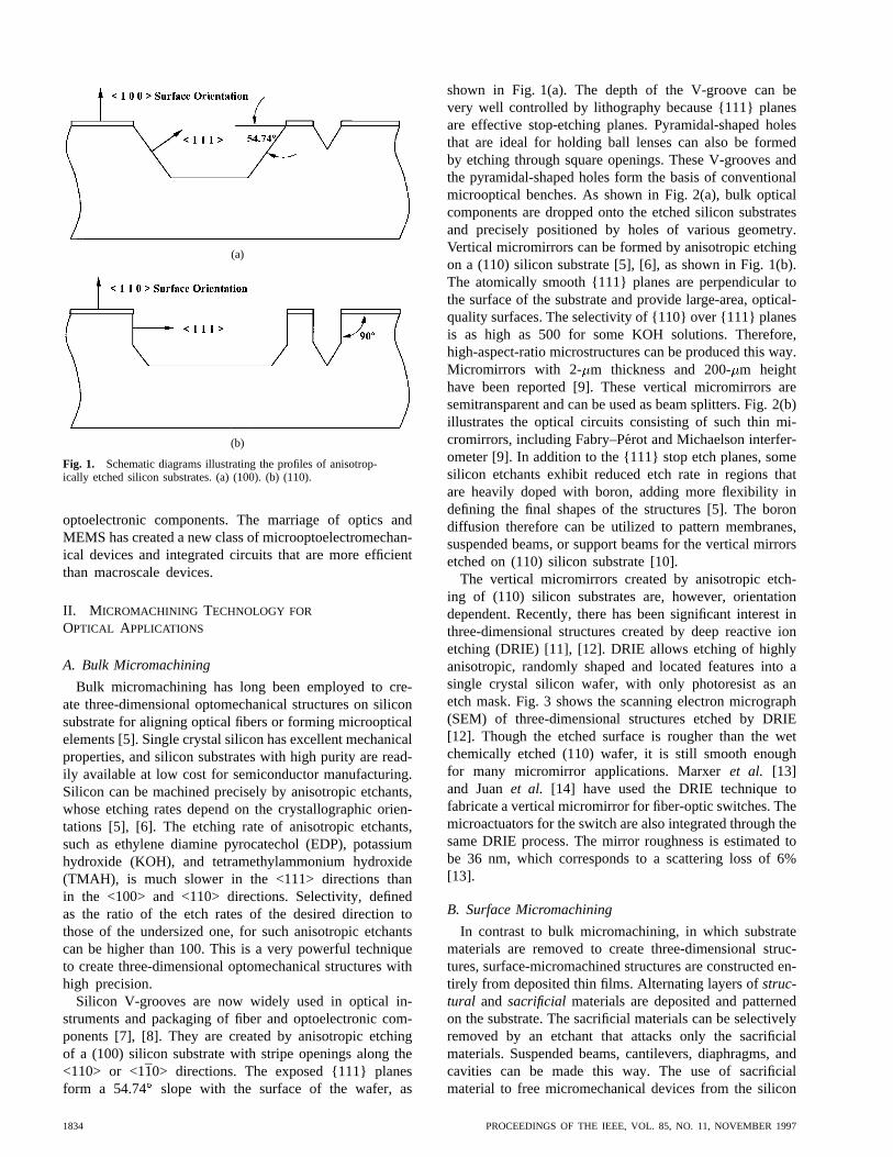
Fig. 1. Schematic diagrams illustrating the profiles of anisotrop-ically etched silicon substrates. (a) (100). (b) (110).
optoelectronic components. The marriage of optics andMEMS has created a new class of microoptoelectromechan-ical devices and integrated circuits that are more efficientthan macroscale devices.
II. M ICROMACHINING TECHNOLOGY FOR
OPTICAL APPLICATIONS
A. Bulk Micromachining
Bulk micromachining has long been employed to cre-ate three-dimensional optomechanical structures on siliconsubstrate for aligning optical fibers or forming microopticalelements [5]. Single crystal silicon has excellent mechanicalproperties, and silicon substrates with high purity are read-ily available at low cost for semiconductor manufacturing.Silicon can be machined precisely by anisotropic etchants,whose etching rates depend on the crystallographic orien-tations [5], [6]. The etching rate of anisotropic etchants,such as ethylene diamine pyrocatechol (EDP), potassiumhydroxide (KOH), and tetramethylammonium hydroxide(TMAH), is much slower in the <111> directions thanin the <100> and <110> directions. Selectivity, definedas the ratio of the etch rates of the desired direction tothose of the undersized one, for such anisotropic etchantscan be higher than 100. This is a very powerful techniqueto create three-dimensional optomechanical structures withhigh precision.
Silicon V-grooves are now widely used in optical in-struments and packaging of fiber and optoelectronic com-ponents [7], [8]. They are created by anisotropic etchingof a (100) silicon substrate with stripe openings along the<110> or <110> directions. The exposed {111} planesform a 54.74 slope with the surface of the wafer, as
shown in Fig. 1(a). The depth of the V-groove can bevery well controlled by lithography because {111} planesare effective stop-etching planes. Pyramidal-shaped holesthat are ideal for holding ball lenses can also be formedby etching through square openings. These V-grooves andthe pyramidal-shaped holes form the basis of conventionalmicrooptical benches. As shown in Fig. 2(a), bulk opticalcomponents are dropped onto the etched silicon substratesand precisely positioned by holes of various geometry.Vertical micromirrors can be formed by anisotropic etchingon a (110) silicon substrate [5], [6], as shown in Fig. 1(b).The atomically smooth {111} planes are perpendicular tothe surface of the substrate and provide large-area, optical-quality surfaces. The selectivity of {110} over {111} planesis as high as 500 for some KOH solutions. Therefore,high-aspect-ratio microstructures can be produced this way.Micromirrors with 2- m thickness and 200-m heighthave been reported [9]. These vertical micromirrors aresemitransparent and can be used as beam splitters. Fig. 2(b)illustrates the optical circuits consisting of such thin mi-cromirrors, including Fabry–P´erot and Michaelson interfer-ometer [9]. In addition to the {111} stop etch planes, somesilicon etchants exhibit reduced etch rate in regions thatare heavily doped with boron, adding more flexibility indefining the final shapes of the structures [5]. The borondiffusion therefore can be utilized to pattern membranes,suspended beams, or support beams for the vertical mirrorsetched on (110) silicon substrate [10].
The vertical micromirrors created by anisotropic etch-ing of (110) silicon substrates are, however, orientationdependent. Recently, there has been significant interest inthree-dimensional structures created by deep reactive ionetching (DRIE) [11], [12]. DRIE allows etching of highlyanisotropic, randomly shaped and located features into asingle crystal silicon wafer, with only photoresist as anetch mask. Fig. 3 shows the scanning electron micrograph(SEM) of three-dimensional structures etched by DRIE[12]. Though the etched surface is rougher than the wetchemically etched (110) wafer, it is still smooth enoughfor many micromirror applications. Marxeret al. [13]and Juanet al. [14] have used the DRIE technique tofabricate a vertical micromirror for fiber-optic switches. Themicroactuators for the switch are also integrated through thesame DRIE process. The mirror roughness is estimated tobe 36 nm, which corresponds to a scattering loss of 6%[13].
B. Surface Micromachining
In contrast to bulk micromachining, in which substratematerials are removed to create three-dimensional struc-tures, surface-micromachined structures are constructed en-tirely from deposited thin films. Alternating layers ofstruc-tural and sacrificial materials are deposited and patternedon the substrate. The sacrificial materials can be selectivelyremoved by an etchant that attacks only the sacrificialmaterials. Suspended beams, cantilevers, diaphragms, andcavities can be made this way. The use of sacrificialmaterial to free micromechanical devices from the silicon
1834 PROCEEDINGS OF THE IEEE, VOL. 85, NO. 11, NOVEMBER 1997

(a)
(b)
Fig. 2. Silicon optical benches on silicon substrates. (a) (100) [7]. (b) (110) (after [9]).
substrate was first demonstrated by Nathansonet al. [15]for fabricating a field effect transistor with a suspendedresonant gate. In 1983, Howe and Muller [16] describedthe use of polysilicon as the structural material and silicondioxide as the sacrificial material. Because of the excellentmechanical properties of polysilicon material and the highselectivity of sacrificial etching with hydrofluoric acid,this combination has become the most popular choice forsurface micromachining.
Fig. 4 illustrates the surface-micromachining process formaking cantilevers. This process requires one layer ofsacrificial material and one layer of structural material.The complexity of the surface-micromachining process canbe quantified by the number of structural and sacrifi-cial materials. With two structural polysilicon layers, free-moving mechanical gears, springs, and sliders have beendemonstrated [17], [18]. Micromotors [19], [20] and other
microactuators were later demonstrated using similar fabri-cation processes. One of the main features that distinguishesthe surface micromachining from the bulk micromachiningis that many different devices can be fabricated using acommon fabrication process. By changing the patterns onthe photomask layouts, different devices such as cantileverresonators, sliders, micromotors, or comb drive actuatorsare fabricated simultaneously on the same substrate. Thismethodology is similar to that used in today’s VLSI circuits.For this reason, the surface-micromachining process is oftenreferred to as an integrated circuit (IC) process or VLSI-like process. Today, there already are two commercialfoundries offering such polysilicon surface-micromachiningprocesses.1 Some of these processes can also be integrated
1MEMS Technology Applications Center, Microelectronics Center atNorth Carolina (MCNC), Research Triangle Park, NC, and Integrated Mi-cro Electro Mechanical Systems, offered at Analog Devices, Cambridge,MA.
WU: MICROMACHINING 1835
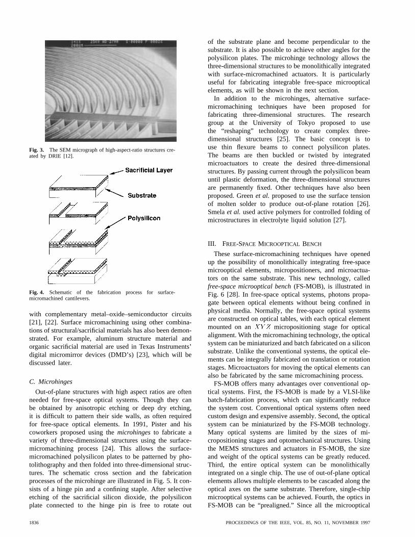
Fig. 3. The SEM micrograph of high-aspect-ratio structures cre-ated by DRIE [12].
Fig. 4. Schematic of the fabrication process for surface-micromachined cantilevers.
with complementary metal–oxide–semiconductor circuits[21], [22]. Surface micromachining using other combina-tions of structural/sacrificial materials has also been demon-strated. For example, aluminum structure material andorganic sacrificial material are used in Texas Instruments’digital micromirror devices (DMD’s) [23], which will bediscussed later.
C. Microhinges
Out-of-plane structures with high aspect ratios are oftenneeded for free-space optical systems. Though they canbe obtained by anisotropic etching or deep dry etching,it is difficult to pattern their side walls, as often requiredfor free-space optical elements. In 1991, Pister and hiscoworkers proposed using themicrohingesto fabricate avariety of three-dimensional structures using the surface-micromachining process [24]. This allows the surface-micromachined polysilicon plates to be patterned by pho-tolithography and then folded into three-dimensional struc-tures. The schematic cross section and the fabricationprocesses of the microhinge are illustrated in Fig. 5. It con-sists of a hinge pin and a confining staple. After selectiveetching of the sacrificial silicon dioxide, the polysiliconplate connected to the hinge pin is free to rotate out
of the substrate plane and become perpendicular to thesubstrate. It is also possible to achieve other angles for thepolysilicon plates. The microhinge technology allows thethree-dimensional structures to be monolithically integratedwith surface-micromachined actuators. It is particularlyuseful for fabricating integrable free-space microopticalelements, as will be shown in the next section.
In addition to the microhinges, alternative surface-micromachining techniques have been proposed forfabricating three-dimensional structures. The researchgroup at the University of Tokyo proposed to usethe “reshaping” technology to create complex three-dimensional structures [25]. The basic concept is touse thin flexure beams to connect polysilicon plates.The beams are then buckled or twisted by integratedmicroactuators to create the desired three-dimensionalstructures. By passing current through the polysilicon beamuntil plastic deformation, the three-dimensional structuresare permanently fixed. Other techniques have also beenproposed. Greenet al. proposed to use the surface tensionof molten solder to produce out-of-plane rotation [26].Smelaet al. used active polymers for controlled folding ofmicrostructures in electrolyte liquid solution [27].
III. FREE-SPACE MICROOPTICAL BENCH
These surface-micromachining techniques have openedup the possibility of monolithically integrating free-spacemicrooptical elements, micropositioners, and microactua-tors on the same substrate. This new technology, calledfree-space microoptical bench(FS-MOB), is illustrated inFig. 6 [28]. In free-space optical systems, photons propa-gate between optical elements without being confined inphysical media. Normally, the free-space optical systemsare constructed on optical tables, with each optical elementmounted on an micropositioning stage for opticalalignment. With the micromachining technology, the opticalsystem can be miniaturized and batch fabricated on a siliconsubstrate. Unlike the conventional systems, the optical ele-ments can be integrally fabricated on translation or rotationstages. Microactuators for moving the optical elements canalso be fabricated by the same micromachining process.
FS-MOB offers many advantages over conventional op-tical systems. First, the FS-MOB is made by a VLSI-likebatch-fabrication process, which can significantly reducethe system cost. Conventional optical systems often needcustom design and expensive assembly. Second, the opticalsystem can be miniaturized by the FS-MOB technology.Many optical systems are limited by the sizes of mi-cropositioning stages and optomechanical structures. Usingthe MEMS structures and actuators in FS-MOB, the sizeand weight of the optical systems can be greatly reduced.Third, the entire optical system can be monolithicallyintegrated on a single chip. The use of out-of-plane opticalelements allows multiple elements to be cascaded along theoptical axes on the same substrate. Therefore, single-chipmicrooptical systems can be achieved. Fourth, the optics inFS-MOB can be “prealigned.” Since all the microoptical
1836 PROCEEDINGS OF THE IEEE, VOL. 85, NO. 11, NOVEMBER 1997
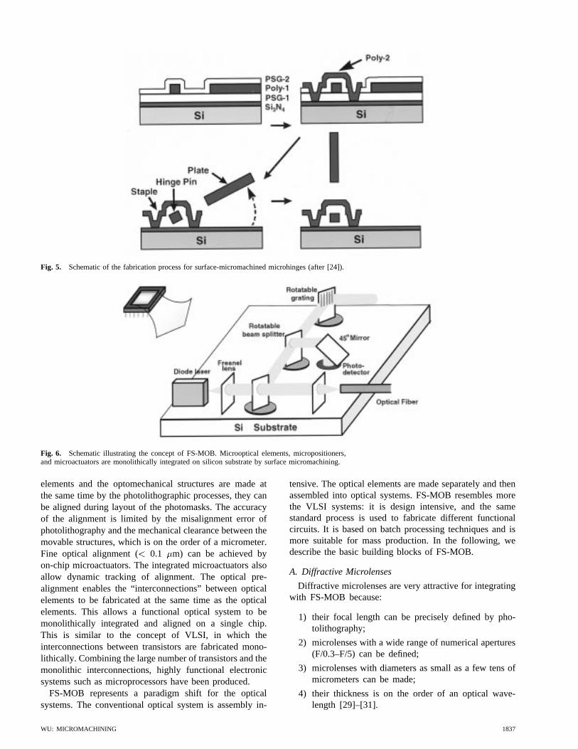
Fig. 5. Schematic of the fabrication process for surface-micromachined microhinges (after [24]).
Fig. 6. Schematic illustrating the concept of FS-MOB. Microoptical elements, micropositioners,and microactuators are monolithically integrated on silicon substrate by surface micromachining.
elements and the optomechanical structures are made atthe same time by the photolithographic processes, they canbe aligned during layout of the photomasks. The accuracyof the alignment is limited by the misalignment error ofphotolithography and the mechanical clearance between themovable structures, which is on the order of a micrometer.Fine optical alignment ( 0.1 m) can be achieved byon-chip microactuators. The integrated microactuators alsoallow dynamic tracking of alignment. The optical pre-alignment enables the “interconnections” between opticalelements to be fabricated at the same time as the opticalelements. This allows a functional optical system to bemonolithically integrated and aligned on a single chip.This is similar to the concept of VLSI, in which theinterconnections between transistors are fabricated mono-lithically. Combining the large number of transistors and themonolithic interconnections, highly functional electronicsystems such as microprocessors have been produced.
FS-MOB represents a paradigm shift for the opticalsystems. The conventional optical system is assembly in-
tensive. The optical elements are made separately and thenassembled into optical systems. FS-MOB resembles morethe VLSI systems: it is design intensive, and the samestandard process is used to fabricate different functionalcircuits. It is based on batch processing techniques and ismore suitable for mass production. In the following, wedescribe the basic building blocks of FS-MOB.
A. Diffractive Microlenses
Diffractive microlenses are very attractive for integratingwith FS-MOB because:
1) their focal length can be precisely defined by pho-tolithography;
2) microlenses with a wide range of numerical apertures(F/0.3–F/5) can be defined;
3) microlenses with diameters as small as a few tens ofmicrometers can be made;
4) their thickness is on the order of an optical wave-length [29]–[31].
WU: MICROMACHINING 1837

(a)
(b)
Fig. 7. (a) Schematic of a Fresnel zone plate. (b) Schematic ofa multiple-level binary microlens.
Fig. 8. Schematic of the out-of-plane micro-Fresnel lens fabri-cated on a hinged polysilicon plate.
The thin construction is particularly suitable for the surface-micromachining process because the thicknesses of thestructural layers are only on the order of 1m. Fig. 7 showsthe schematic diagram of two diffractive microlenses: (a)Fresnel lens and (b) multiple-level binary microlens. Thebinary-amplitude Fresnel zone plate has alternating trans-mission and blocking zones. Though it is very easy tofabricate, however, its efficiency (diffraction efficiency intothe first-order beam) is limited to 10%. The efficiency of abinary microlens with phase levels is [29]
The efficiency increases with the number of phase levels atthe expense of more complicated fabrication processes. Forexample, 41% for , 81% for , and
99% for . Fabrication of binary microlenses onvarious substrates has already been demonstrated [29]–[31].These microlenses are usually confined to the surface ofthe substrates.
Microlenses with optical axes parallel to the substrateare necessary for single-chip microoptical systems. Thisis achieved by combining the conventional microopticstechnology with the surface-micromachined microhinges.As shown in Fig. 8, the micro-Fresnel lens is fabricated on
Fig. 9. The assembly process for the three-dimensional mi-cro-Fresnel lens.
Fig. 10. The SEM of the out-of-plane micro-Fresnel lens. Thelens has a diameter of 280�m, a focal length of 500�m, and anoptical axis of 254�m above the silicon substrate.
a hinged polysilicon plate [32], [33]. Since the polysiliconplate lies on the surface of the substrate before assembly,conventional planar fabrication technology can be used todefine the patterns of the Fresnel lens. After releasing etch,the micro-Fresnel lens plate is rotated out of the substrateplane and becomes perpendicular to the substrate. Theassembly process is illustrated in Fig. 9. To enhance themechanical strength and to more precisely define the angleof the microlens, a pair of side support plates is added. Theside support plates are also made on polysilicon using themicrohinge technology. They have a V-shaped opening atthe top, followed by a long, narrow groove in the center.When they are folded onto the microlens plate, the 2-m-thick microlens plate is firmly locked into the 2.5-m-widegroove. As will be shown later, the side support plates playa critical role in the robustness of such three-dimensionalmicrostructures. The maximum angular variation of themicrolens depends on the geometry of the side supportplates. Angular variation of less than 0.1is achievable.Fig. 10 shows the SEM micrograph of a micro-Fresnel lenswith a diameter of 280 m, a focal length of 500 m, andan optical axis of 254 m above the silicon surface [33].For simplicity, only a binary-amplitude Fresnel zone plate
1838 PROCEEDINGS OF THE IEEE, VOL. 85, NO. 11, NOVEMBER 1997

Fig. 11. The intensity profile and contour plot of the optical beamemitted from an optical fiber and collimated by the micro-Fresnellens.
is demonstrated. Lenses as large as 650m and as tall as1.4 mm also have been demonstrated [32].
The lens exhibits very good optical performance. Theoutput beam from a single-mode fiber is successfullycollimated by the lens [32]. Fig. 11 shows the intensityprofile of the collimated beam and the contour plotof the intensity distribution. Very good agreement withGaussian shape is obtained. The intensity full-width-at-half-maximum (FWHM) divergence angle of the collimatedbeam has been reduced from 5.0to 0.33 . The diffractionefficiency of the micro-Fresnel lens was measured tobe 8.6% using the method described by Rastaniet al.[30]. This is in agreement with the theoretical limit ofthe binary-amplitude Fresnel zone plate. As mentionedearlier, efficiency greater than 80% can be achievedby multilevel Fresnel lenses at the expense of morecomplicated fabrication processes. Another potential issueof fabricating diffractive optical elements on the surface-micromachined polysilicon plates is the surface roughness.The plates might need to be smoothened by chemical-mechanical planarization, which can reduce the surfaceroughness to 17A [34]. Another alternative to achievehigh efficiency is to use a refractive lens, as described inthe next section.
B. Refractive Microlenses
The refractive microlenses are complementary to thediffractive microlenses. They offer several advantages over
Fig. 12. Schematic of an out-of-plane refractive microlens.
diffractive optical elements. Their focal length is indepen-dent of the optical wavelength (except a weak dependencedue to the dispersion of the lens material). It is also easierto make fast refractive microlenses without tight criticaldimension control. Refractive microlenses do not sufferfrom diffraction loss, and it is easier to make a high-efficiency lens at low cost. In contrast, high-efficiencydiffractive microlenses need multiple critical lithographysteps.
Fabrication of a planar refractive microlens arrayon semiconductor and dielectric substrates has beendemonstrated using photoresist/polyimide reflow techniques[35]–[38]. The lens pattern can also be transferred tosubstrate through reactive ion etching or ion milling. Here,we combine the planar refractive microlens fabrication withthe surface-micromachining process to create low-cost,high-quality out-of-plane refractive microlenses. Fig. 12shows the schematic drawing of the out-of-plane refractivespherical lens [39]. One potential issue for such microlensesis the scattering loss of the supporting polysilicon plate.The scattering loss is related to the surface roughness by[13], [40]
where is the percentage of the scattering loss,is theroot-mean-square roughness of the polysilicon surface,is the incident angle, and is the optical wavelength.The surface roughness of as-grown polysilicon is on theorder of 45 nm (the exact value depends on the depositioncondition), and the corresponding scattering loss is 17% perinterface at 1300-nm wavelength. There are two approachesto reducing the scattering loss. The first is to smooth thesurface by chemical-mechanical planarization (CMP). Thesurface roughness can be reduced to 1.7 nm, which willimprove the scattering loss to 0.02%. Both surfaces needto be polished for a transmission device, however, and it isdifficult to polish the bottom side of the polysilicon plate.Alternatively, we can remove the polysilicon material atthe center of the lens, which forms an aperture for the
WU: MICROMACHINING 1839

Fig. 13. The fabrication process for the three-dimensional refrac-tive microlens. The microlens is fabricated on a hinged polysiliconplate by the reflow technique.
Fig. 14. The surface profile of the microlens. The lens is 30�mthick at center and 300�m in diameter.
microlens. The scattering as well as reflection loss of thepolysilicon plate are thus eliminated. We have adopted thesecond approach here.
The fabrication process is illustrated in Fig. 13 [39]. First,a lens mount is fabricated using the surface-micromachiningtechnique. This process is similar to that of the micro-Fresnel lens except that an aperture is etched in the centerof the polysilicon plate. Before releasing, a 20-m-thickAZ 4620 photoresist cylinder is deposited on the hingedpolysilicon plate. The lens is realized by heating the pho-toresist cylinder to 200C, causing the photoresist to reflowinto a spherical shape. Fig. 14 shows the surface profileof the reflowed photoresist. The lens is 30m thick atcenter, and the maximum deviation from spherical is lessthan 0.5 m to within 5 m of the edges. The resultinglens has a diameter of 300m and a focal length of670 m. Refractive microlenses with an F-number rangingfrom one to five and diameters from 30 to more than 500
m can be made by this technique. The microlens can bemade vertical to the substrate by rotating the supportingpolysilicon plate after the reflow processes. Fig. 15 showsthe SEM micrographs of both the front and back sides of themicrolens. The back-side view clearly shows the aperture ofthe microlens. The optical loss of the microlens is measured
Fig. 15. SEM micrographs of the front and back sides of thethree-dimensional refractive microlens. The aperture of the mi-crolens is clearly visible from the backside.
to be 0.7 dB at 632-nm wavelength. Lower loss is expectedat longer wavelengths. The optical axis of the microlensesis fixed to the same height as the rest of the FS-MOB byphotolithography. Therefore, the refractive microlens can bealigned to other optical elements to within the fabricationtolerance.
Very good optical performance has been achieved for therefractive microlens. The divergence angle of the light emit-ted from a single-mode fiber at 630 nm has been reducedfrom 3.3 to 0.18 after it is collimated by the refractivemicrolens. The intensity contour of the collimated beam isalso very symmetric, as shown in Fig. 16, indicating thehigh quality of the spherical microlens.
C. Micropositioners
As described in [17] and [18], various types of movablestructures can be made by the surface-micromachining
1840 PROCEEDINGS OF THE IEEE, VOL. 85, NO. 11, NOVEMBER 1997

Fig. 16. The intensity contour of the optical beam collimated bythe spherical microlens.
Fig. 17. Surface-micromachined translation stage with (a) flexuresprings and (b) sliding guides.
technique. A linear translation stage and rotation stage canbe built in a similar way on FS-MOB. The microlensesand other out-of-plane microoptical elements can be inte-grated with translation and rotation stages by attaching themicrohinges to a movable polysilicon plate. The movablestage consists of a fully released polysilicon plate that isattached or confined to the substrate by either 1) flexuresprings or 2) sliding guides. Fig. 17 illustrates these twotypes of micropositioners. The spring-attached stage is moreaccurate; however, it has limited travel distance. The springrestoring force also needs to be constantly balanced bythe actuators. The sliding type of stage has a long traveldistance. Since there is no restoring force, the frictionbetween the stage and the substrate or the sliding guides canhold the stage in place without any power consumption. Onthe other hand, the finite clearance between the stage andthe sliding guides may cause some statistical variation andhysteresis. These two types of stages are complementary.
To integrate the microoptical elements on translationstages, the microoptics plate now needs to be constructedon the second polysilicon layer and connected to themicrohinges defined on the first polysilicon layer. The basesof the spring latched and staples are now connected to themovable plate on the first polysilicon layer instead of thesubstrate. Fig. 18 shows the SEM micrograph of a three-dimensional micrograting integrated on a rotation stage[41]. The stage in the SEM has been rotated by 20. Therotary grating has been employed to build an integrated-wavelength meter for a single-wavelength laser [42] andmicrospectrometer [43].
D. Microactuators
Perhaps the most interesting feature of micromachinedoptics is the ability to integrate microactuators with the
Fig. 18. SEM micrograph of a three-dimensional microgratingintegrated on a rotation stage.
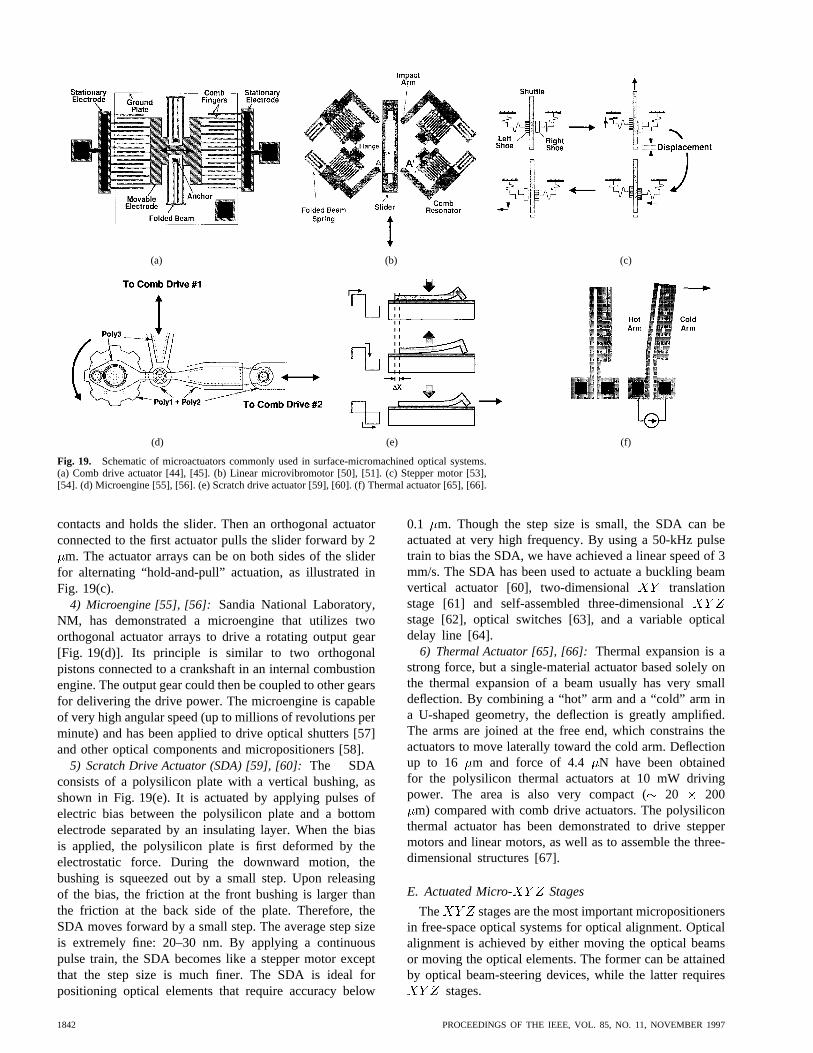
optical elements. Many new surface-micromachined mi-croactuators have been proposed and demonstrated sincethe invention of micromotors. It is beyond the scope of thispaper to have a complete review of these microactuators.Here, we will describe only a selected set of microactuatorsthat are particularly useful for optical applications. Fig. 19shows the schematic drawing of these actuators.
1) Comb Drive Actuator [44], [45]: The comb drive isactuated by electrostatic force between a pair of movablecombs and fixed combs, as shown in Fig. 19(a). Whena voltage is applied, the movable comb is attracted tothe stationary comb. The position of the movable combcan thus be controlled by voltage. This is perhaps by farthe most popular surface-micromachined actuator. Typicalsurface-micromachined polysilicon comb drive actuatorscan produce micronewtons of force and a few micrometersof displacement. The comb drive actuators have beenemployed to drive optical choppers [46] and bar-codescanners [47]. Another electrostatic actuator is gap-closingactuators [48], [49]. They have larger force but smallerdisplacement.
2) Linear Microvibromotor [50], [51]: Impact actuationcan be used to obtain relatively large motion from small-displacement resonant structures such as comb driveactuators. The linear microvibromotor shown in Fig. 19(b)consists of two 45 resonant comb drives, two 45resonant comb drives, and a slider. Upon each impact fromthe comb drives, the slider moves by an average step sizeof 0.27 m [51]. The standard deviation of the step size isrelatively large (0.17 m) due to the impact actuation andwobble of the slider. The position and speed of the slidercan be controlled by adjusting the number of impacts. Amaximum speed of 1 mm/s has been achieved. The linearmicrovibromotor has been used to actuate a slide-tilt mirrorfor alignment for optical beams for fiber coupling [52].
3) Stepper Motor: In addition to impact actuation, thelong travel distance of the slider can also be achieved by the“hold-and-pull” actuation [53], [54]. A large-force, small-displacement actuator, such as the gap-closing actuator, first
WU: MICROMACHINING 1841
(a) (b) (c)
(d) (e) (f)
Fig. 19. Schematic of microactuators commonly used in surface-micromachined optical systems.(a) Comb drive actuator [44], [45]. (b) Linear microvibromotor [50], [51]. (c) Stepper motor [53],[54]. (d) Microengine [55], [56]. (e) Scratch drive actuator [59], [60]. (f) Thermal actuator [65], [66].
contacts and holds the slider. Then an orthogonal actuatorconnected to the first actuator pulls the slider forward by 2
m. The actuator arrays can be on both sides of the sliderfor alternating “hold-and-pull” actuation, as illustrated inFig. 19(c).
4) Microengine [55], [56]: Sandia National Laboratory,NM, has demonstrated a microengine that utilizes twoorthogonal actuator arrays to drive a rotating output gear[Fig. 19(d)]. Its principle is similar to two orthogonalpistons connected to a crankshaft in an internal combustionengine. The output gear could then be coupled to other gearsfor delivering the drive power. The microengine is capableof very high angular speed (up to millions of revolutions perminute) and has been applied to drive optical shutters [57]and other optical components and micropositioners [58].
5) Scratch Drive Actuator (SDA) [59], [60]:The SDAconsists of a polysilicon plate with a vertical bushing, asshown in Fig. 19(e). It is actuated by applying pulses ofelectric bias between the polysilicon plate and a bottomelectrode separated by an insulating layer. When the biasis applied, the polysilicon plate is first deformed by theelectrostatic force. During the downward motion, thebushing is squeezed out by a small step. Upon releasingof the bias, the friction at the front bushing is larger thanthe friction at the back side of the plate. Therefore, theSDA moves forward by a small step. The average step sizeis extremely fine: 20–30 nm. By applying a continuouspulse train, the SDA becomes like a stepper motor exceptthat the step size is much finer. The SDA is ideal forpositioning optical elements that require accuracy below
0.1 m. Though the step size is small, the SDA can beactuated at very high frequency. By using a 50-kHz pulsetrain to bias the SDA, we have achieved a linear speed of 3mm/s. The SDA has been used to actuate a buckling beamvertical actuator [60], two-dimensional translationstage [61] and self-assembled three-dimensionalstage [62], optical switches [63], and a variable opticaldelay line [64].
6) Thermal Actuator [65], [66]: Thermal expansion is astrong force, but a single-material actuator based solely onthe thermal expansion of a beam usually has very smalldeflection. By combining a “hot” arm and a “cold” arm ina U-shaped geometry, the deflection is greatly amplified.The arms are joined at the free end, which constrains theactuators to move laterally toward the cold arm. Deflectionup to 16 m and force of 4.4 N have been obtainedfor the polysilicon thermal actuators at 10 mW drivingpower. The area is also very compact (20 200
m) compared with comb drive actuators. The polysiliconthermal actuator has been demonstrated to drive steppermotors and linear motors, as well as to assemble the three-dimensional structures [67].
E. Actuated Micro- Stages
The stages are the most important micropositionersin free-space optical systems for optical alignment. Opticalalignment is achieved by either moving the optical beamsor moving the optical elements. The former can be attainedby optical beam-steering devices, while the latter requires
stages.
1842 PROCEEDINGS OF THE IEEE, VOL. 85, NO. 11, NOVEMBER 1997
(a)
(b)
Fig. 20. (a) Schematic of vertical beam-shifting device. (b)Schematic of three-dimensional beam-steering device.
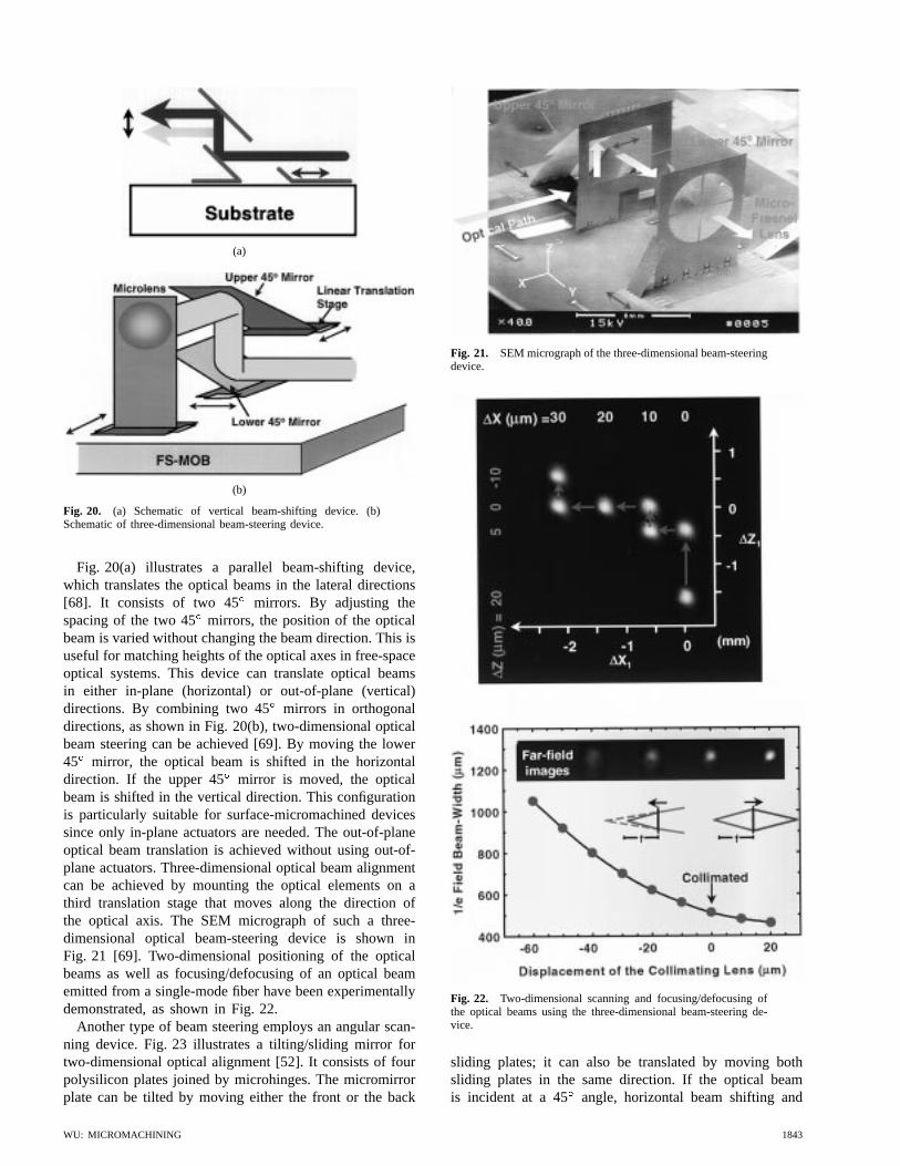
Fig. 20(a) illustrates a parallel beam-shifting device,which translates the optical beams in the lateral directions[68]. It consists of two 45 mirrors. By adjusting thespacing of the two 45mirrors, the position of the opticalbeam is varied without changing the beam direction. This isuseful for matching heights of the optical axes in free-spaceoptical systems. This device can translate optical beamsin either in-plane (horizontal) or out-of-plane (vertical)directions. By combining two 45 mirrors in orthogonaldirections, as shown in Fig. 20(b), two-dimensional opticalbeam steering can be achieved [69]. By moving the lower45 mirror, the optical beam is shifted in the horizontaldirection. If the upper 45 mirror is moved, the opticalbeam is shifted in the vertical direction. This configurationis particularly suitable for surface-micromachined devicessince only in-plane actuators are needed. The out-of-planeoptical beam translation is achieved without using out-of-plane actuators. Three-dimensional optical beam alignmentcan be achieved by mounting the optical elements on athird translation stage that moves along the direction ofthe optical axis. The SEM micrograph of such a three-dimensional optical beam-steering device is shown inFig. 21 [69]. Two-dimensional positioning of the opticalbeams as well as focusing/defocusing of an optical beamemitted from a single-mode fiber have been experimentallydemonstrated, as shown in Fig. 22.
Another type of beam steering employs an angular scan-ning device. Fig. 23 illustrates a tilting/sliding mirror fortwo-dimensional optical alignment [52]. It consists of fourpolysilicon plates joined by microhinges. The micromirrorplate can be tilted by moving either the front or the back
Fig. 21. SEM micrograph of the three-dimensional beam-steeringdevice.
Fig. 22. Two-dimensional scanning and focusing/defocusing ofthe optical beams using the three-dimensional beam-steering de-vice.
sliding plates; it can also be translated by moving bothsliding plates in the same direction. If the optical beamis incident at a 45 angle, horizontal beam shifting and
WU: MICROMACHINING 1843
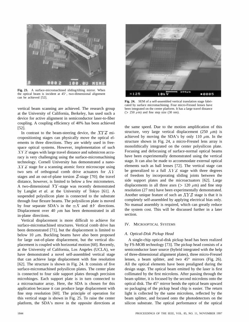
Fig. 23. A surface-micromachined sliding/tilting mirror. Whenthe optical beam is incident at 45�, two-dimensional alignmentcan be achieved [52].
vertical beam scanning are achieved. The research groupat the University of California, Berkeley, has used such adevice for active alignment in semiconductor laser-to-fibercoupling. A coupling efficiency of 40% has been achieved[52].
In contrast to the beam-steering device, the mi-cropositioning stages can physically move the optical el-ements in three directions. They are widely used in free-space optical systems. However, implementation of such
stages with large travel distance and submicron accu-racy is very challenging using the surface-micromachiningtechnology. Cornell University has demonstrated a nano-
stage for a scanning atomic force microscope usingtwo sets of orthogonal comb drive actuators forstages and an out-of-plane torsion-stage [70]; the traveldistance, however, is limited to below a few micrometers.A two-dimensional -stage was recently demonstratedby Langlet et al. at the University of Tokyo [61]. Asuspended polysilicon plate is connected to the substratethrough four flexure beams. The polysilicon plate is movedby four separate SDA’s in the and directions.Displacement over 40 m has been demonstrated in allin-plane directions.
Vertical displacement is more difficult to achieve forsurface-micromachined structures. Vertical comb drive hasbeen demonstrated [71], but the displacement is limited tobelow 10 m. Buckling beams have also been proposedfor large out-of-plane displacement, but the vertical dis-placement is coupled with horizontal motion [60]. Recently,at the University of California, Los Angeles (UCLA), wehave demonstrated a novel self-assembled vertical stagethat can achieve large displacement with fine resolution[62]. The structure is shown in Fig. 24. It consists of fivesurface-micromachined polysilicon plates. The center plateis connected to four side support plates through precisionmicrohinges. Each support plate is in turn connected toa microactuator array. Here, the SDA is chosen for thisapplication because it can produce large displacement withfine step resolution [60]. The principle of operation forthis vertical stage is shown in Fig. 25. To raise the centerplatform, the SDA’s move in the opposite directions at
Fig. 24. SEM of a self-assembled vertical translation stage fabri-cated by surface micromachining. Four micro-Fresnel lenses havebeen integrated on the center platform. It has a large travel distance(> 250 �m) and fine step size (30 nm).
the same speed. Due to the motion amplification of thisstructure, very large vertical displacement (250m) isachieved by moving the SDA’s by only 110m. In thestructure shown in Fig. 24, a micro-Fresnel lens array ismonolithically integrated on the center polysilicon plate.Focusing and defocusing of surface-normal optical beamshave been experimentally demonstrated using the verticalstage. It can also be made to accommodate external opticalelements such as ball lenses [72]. The vertical stage canbe generalized to a full stage with three degreesof freedom by incorporating sliding joints between theside support plates and the microactuators [62]. Largedisplacements in all three axes (120 m) and fine stepresolution (27 nm) have been experimentally demonstrated.Another unique feature of such an stage is that it iscompletely self-assembled by applying electrical bias only.No manual assembly is required, which can greatly reducethe system cost. This will be discussed further in a latersection.
IV. M ICROOPTICAL SYSTEMS
A. Optical-Disk Pickup Head
A single-chip optical-disk pickup head has been realizedby FS-MOB technology [73]. The pickup head consists of asemiconductor laser source (hybrid integrated with the helpof three-dimensional alignment plates), three micro-Fresnellenses, a beam splitter, and two 45mirrors (Fig. 26).All the optical elements have been prealigned during thedesign stage. The optical beam emitted by the laser is firstcollimated by the first microlens. After passing through thebeam splitter, it is focused by the second microlens onto theoptical disk. The 45 mirror bends the optical beam upwardso packaging of the pickup head chip is easier. The returnlight is collected by the same microlens, reflected by thebeam splitter, and focused onto the photodetectors on thesilicon substrate. The optical performance of the optical
1844 PROCEEDINGS OF THE IEEE, VOL. 85, NO. 11, NOVEMBER 1997
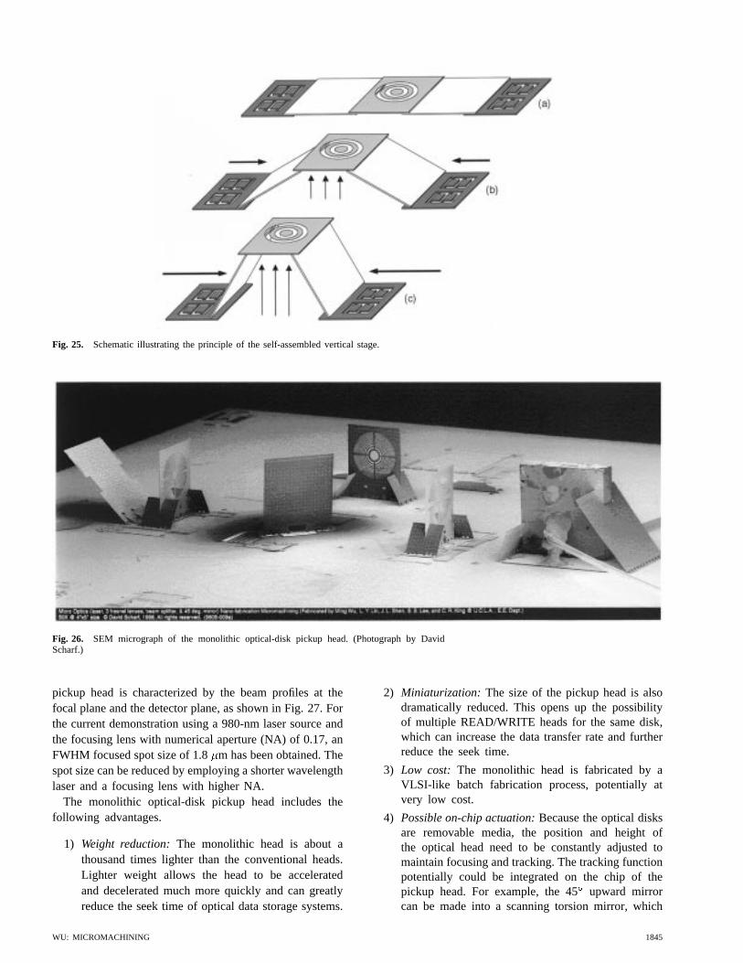
Fig. 25. Schematic illustrating the principle of the self-assembled vertical stage.
Fig. 26. SEM micrograph of the monolithic optical-disk pickup head. (Photograph by DavidScharf.)
pickup head is characterized by the beam profiles at thefocal plane and the detector plane, as shown in Fig. 27. Forthe current demonstration using a 980-nm laser source andthe focusing lens with numerical aperture (NA) of 0.17, anFWHM focused spot size of 1.8m has been obtained. Thespot size can be reduced by employing a shorter wavelengthlaser and a focusing lens with higher NA.
The monolithic optical-disk pickup head includes thefollowing advantages.
1) Weight reduction:The monolithic head is about athousand times lighter than the conventional heads.Lighter weight allows the head to be acceleratedand decelerated much more quickly and can greatlyreduce the seek time of optical data storage systems.
2) Miniaturization: The size of the pickup head is alsodramatically reduced. This opens up the possibilityof multiple READ/WRITE heads for the same disk,which can increase the data transfer rate and furtherreduce the seek time.
3) Low cost: The monolithic head is fabricated by aVLSI-like batch fabrication process, potentially atvery low cost.
4) Possible on-chip actuation:Because the optical disksare removable media, the position and height ofthe optical head need to be constantly adjusted tomaintain focusing and tracking. The tracking functionpotentially could be integrated on the chip of thepickup head. For example, the 45upward mirrorcan be made into a scanning torsion mirror, which
WU: MICROMACHINING 1845
Fig. 27. The profile of the optical beam focused on the surface of the disk and on the photodetectorplane.
can scan the focused beam across the tracks of theoptical disks.
B. Femtosecond Autocorrelator
Another example of a single-chip microoptical system isthe monolithic femtosecond autocorrelator. The autocorre-lator is an optical instrument for measuring the durationof ultrashort optical pulses with femtosecond resolution. Itconsists of an interferometer with a variable delay arm anda nonlinear detector. In principle, the autocorrelator can bemade very compact because one femtosecond correspondsto a distance of 0.3 m. In reality, it is limited by thesize of bulk optics, micromechanical stages, and motors,and typical autocorrelators are larger than the size of ashoebox. With FS-MOB, it is possible to monolithicallyintegrate the autocorrelator on a single chip. The SEMmicrograph of the autocorrelator is shown in Fig. 28 [64].It consists of a microactuated translation stage, two beamsplitters, and six micromirrors integrated on an Si chip withan area of 4 4.5 mm . All the microoptical elements arebuilt monolithically on the Si substrate, with their opticalaxes parallel to the substrate. A collinear configuration isemployed for the first demonstration. Since the FS-MOBcan be prealigned during layout of the photomasks, thetwo optical path lengths are balanced to almost zero initialdifferential delay. The two beams combine collinearly atthe output beam splitter. The variable delay line comprisesa two-mirror retroreflector and a microactuated translationstage. It is driven by the SDA’s discussed earlier. Theyhave a large travel distance and a fine step size of 27nm, which corresponds to a temporal resolution of 0.18fs. We have employed a two-photon-absorption (TPA)photodiode as the nonlinear detector. The semiconductorphotodiode can potentially be integrated on the Si substrate.A silicon photodiode can be used for TPA for wavelengthsof 1.1–2.2 m, which covers the spectrum used for fiber
communications. Here, we use an InGaP photodiode fordetecting the 860-nm femtosecond pulses generated by theTi:Sapphire laser. The experimental autocorrelation resultsobtained from the micromachined autocorrelators with TPAphotodiode and the conventional autocorrelator with non-linear crystal are shown in Fig. 29(a) and (b), respectively.Very good agreement has been obtained. The speed of SDAranges from micrometers/second to 3 mm/s. Therefore, thetime required for completing one autocorrelation trace (scanover 1 ps) can be as short as 0.1 s.
C. Fiber-Optic Switches
Free-space fiber-optic switches offer many advantagesover conventional waveguide switches. They have lowercoupling loss and much smaller cross talk, and are inde-pendent of wavelength, polarization, and data format. Boththe surface-micromachining and the bulk-micromachiningtechniques have been used to fabricate fiber-optic switches.A bulk-micromachined 2 2 fiber-optic switch was re-ported by AT&T Bell Laboratories in 1992 [74]. A (110)silicon wafer is anisotropically etched by EDP to createsmooth vertical micromirrors. Very high reflectivity (97%) has been achieved for these single crystalline mirrorswhen coated with Ti/Pt/Au coating. A separate (100) siliconsubstrate is chemically etched to create four V-grooves andpyramidal holes for aligning fibers and ball lenses. Thetwo wafers are then joined together manually, and externalactuators are employed. An insertion loss of 0.7 dB and aswitching time of less than 10 ms have been obtained. Thisswitch still requires substantial assembly, however, and thepotential cost is high. In the following, we will describe therecent progress in micromachined fiber-optic switches.
1) Surface-Micromachined Fiber-Optic Switches:Underthe support of the Defense Advance Research ProjectAgency, UCLA and the Rockwell Science Center havebeen investigating manufacturable, low-cost fiber-optic
1846 PROCEEDINGS OF THE IEEE, VOL. 85, NO. 11, NOVEMBER 1997

Fig. 28. The schematic and SEM of the femtosecond autocorrelator.
Fig. 29. Experimental autocorrelation traces. (a) Measured by the MEMS autocorrelator witha TPA photodetector. (b) Measured by the conventional autocorrelator with second harmonicgeneration crystal.
switches using surface-micromachining technologies since1994 [75]. Surface micromachining offers greater flexibilitysince it can monolithically integrate various types of three-dimensional microoptical elements with microactuators.The schematic diagram of the switch is shown in Fig. 30.It consists of a movable three-dimensional micromirror,four fiber guiding rails, and microacuators. Depending onthe mirror position, light emitted from the input fiber iseither transmitted to the opposite fiber or reflected to theorthogonal fiber. By keeping the distance between fibersshort, it is possible to achieve low insertion loss withoutexternal lenses. For multimode fibers with higher numericalaperture, a semispherical fiber lens can be used to reducethe diffraction loss and to increase the working distance.The mirror is actuated by the SDA microactuators. Insteadof using two actuators to move the mirror back and forth,we employ a mechanical flexure spring to pull the SDA
back to the center position. This is necessary for the “fail-safe” requirement, i.e., the switch must always return to thebypass state during power failure. Since the SDA force islarger than the spring force, the mirror is moved away bythe SDA’s when an ac electrical pulse train is applied to theSDA’s. The mirror can be maintained at the off-centeredposition by applying a dc bias to hold the SDA’s to thesubstrate. When the dc voltage is released, or when powerfailure occurs, the mirror will return to the center positionby the spring force. This 2 2 has been fabricated by thethree-polysilicon-layer surface-micromachining technologyoffered at MCNC. The SEM micrograph of the switch isshown in Fig. 31 [63].
The optical performance of the switch has been character-ized using four multimode optical fibers with 62.5-m corediameters. The fiber-to-fiber spacing is 80m, and the fibertip has been melted to form hemispherical microlenses. The
WU: MICROMACHINING 1847
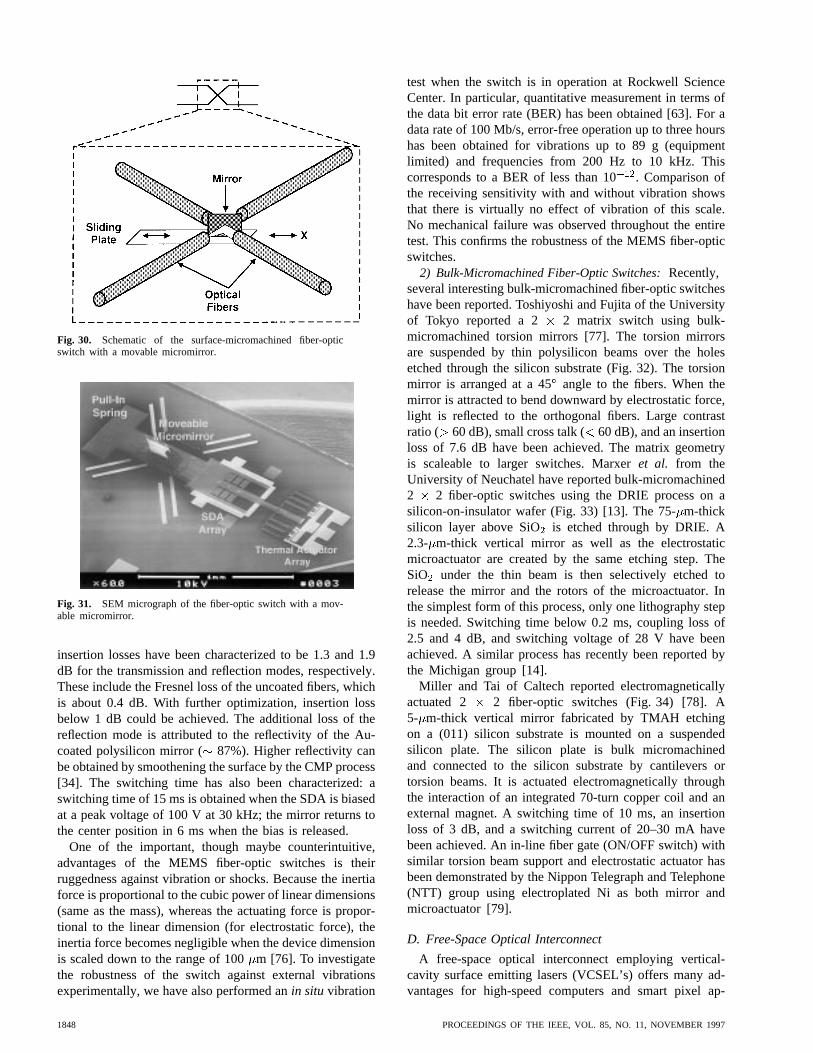
Fig. 30. Schematic of the surface-micromachined fiber-opticswitch with a movable micromirror.
Fig. 31. SEM micrograph of the fiber-optic switch with a mov-able micromirror.
insertion losses have been characterized to be 1.3 and 1.9dB for the transmission and reflection modes, respectively.These include the Fresnel loss of the uncoated fibers, whichis about 0.4 dB. With further optimization, insertion lossbelow 1 dB could be achieved. The additional loss of thereflection mode is attributed to the reflectivity of the Au-coated polysilicon mirror ( 87%). Higher reflectivity canbe obtained by smoothening the surface by the CMP process[34]. The switching time has also been characterized: aswitching time of 15 ms is obtained when the SDA is biasedat a peak voltage of 100 V at 30 kHz; the mirror returns tothe center position in 6 ms when the bias is released.
One of the important, though maybe counterintuitive,advantages of the MEMS fiber-optic switches is theirruggedness against vibration or shocks. Because the inertiaforce is proportional to the cubic power of linear dimensions(same as the mass), whereas the actuating force is propor-tional to the linear dimension (for electrostatic force), theinertia force becomes negligible when the device dimensionis scaled down to the range of 100m [76]. To investigatethe robustness of the switch against external vibrationsexperimentally, we have also performed anin situ vibration
test when the switch is in operation at Rockwell ScienceCenter. In particular, quantitative measurement in terms ofthe data bit error rate (BER) has been obtained [63]. For adata rate of 100 Mb/s, error-free operation up to three hourshas been obtained for vibrations up to 89 g (equipmentlimited) and frequencies from 200 Hz to 10 kHz. Thiscorresponds to a BER of less than 10. Comparison ofthe receiving sensitivity with and without vibration showsthat there is virtually no effect of vibration of this scale.No mechanical failure was observed throughout the entiretest. This confirms the robustness of the MEMS fiber-opticswitches.
2) Bulk-Micromachined Fiber-Optic Switches:Recently,several interesting bulk-micromachined fiber-optic switcheshave been reported. Toshiyoshi and Fujita of the Universityof Tokyo reported a 2 2 matrix switch using bulk-micromachined torsion mirrors [77]. The torsion mirrorsare suspended by thin polysilicon beams over the holesetched through the silicon substrate (Fig. 32). The torsionmirror is arranged at a 45angle to the fibers. When themirror is attracted to bend downward by electrostatic force,light is reflected to the orthogonal fibers. Large contrastratio ( 60 dB), small cross talk ( 60 dB), and an insertionloss of 7.6 dB have been achieved. The matrix geometryis scaleable to larger switches. Marxeret al. from theUniversity of Neuchatel have reported bulk-micromachined2 2 fiber-optic switches using the DRIE process on asilicon-on-insulator wafer (Fig. 33) [13]. The 75-m-thicksilicon layer above SiO is etched through by DRIE. A2.3- m-thick vertical mirror as well as the electrostaticmicroactuator are created by the same etching step. TheSiO under the thin beam is then selectively etched torelease the mirror and the rotors of the microactuator. Inthe simplest form of this process, only one lithography stepis needed. Switching time below 0.2 ms, coupling loss of2.5 and 4 dB, and switching voltage of 28 V have beenachieved. A similar process has recently been reported bythe Michigan group [14].
Miller and Tai of Caltech reported electromagneticallyactuated 2 2 fiber-optic switches (Fig. 34) [78]. A5- m-thick vertical mirror fabricated by TMAH etchingon a (011) silicon substrate is mounted on a suspendedsilicon plate. The silicon plate is bulk micromachinedand connected to the silicon substrate by cantilevers ortorsion beams. It is actuated electromagnetically throughthe interaction of an integrated 70-turn copper coil and anexternal magnet. A switching time of 10 ms, an insertionloss of 3 dB, and a switching current of 20–30 mA havebeen achieved. An in-line fiber gate (ON/OFF switch) withsimilar torsion beam support and electrostatic actuator hasbeen demonstrated by the Nippon Telegraph and Telephone(NTT) group using electroplated Ni as both mirror andmicroactuator [79].
D. Free-Space Optical Interconnect
A free-space optical interconnect employing vertical-cavity surface emitting lasers (VCSEL’s) offers many ad-vantages for high-speed computers and smart pixel ap-
1848 PROCEEDINGS OF THE IEEE, VOL. 85, NO. 11, NOVEMBER 1997

Fig. 32. Schematic of a matrix fiber-optic switch with torsion mirrors [77].
Fig. 33. Schematic of a 2� 2 fiber-optic switch with verticalmirror fabricated by DRIE [13].
plications. The optical beams emitted from VCSEL’s areusually expanded, collimated, or focused by external mi-crolenses. Monolithic integration of fixed refractive [80]and diffractive [81] microlenses on the back side of VC-SEL wafers has been demonstrated. In most applications,however, it is desirable to have a dynamically movablemicrolens on top of the VCSEL to perform dynamic opticalalignment, tracking and focusing, continuous optical beam
Fig. 34. Schematic of a 2� 2 fiber-optic switch with (110)etched mirror and electromagnetic actuator [78].
scanning, space division switching, or implementation ofreconfigurable optical interconnect.
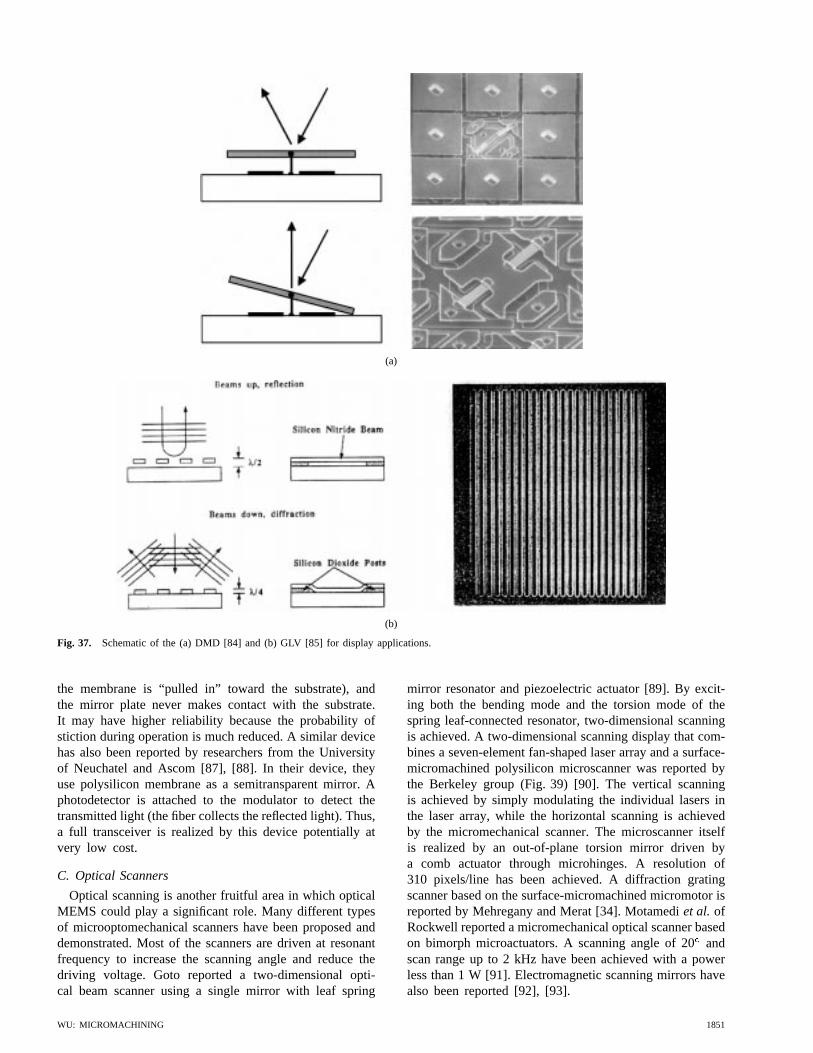
We have used the surface-micromachining technologyto produce a suspended microlens for dynamic alignmentin free-space optical interconnect. Fig. 35 shows the SEMmicrograph of the suspended scanning microlens [82].A 670-nm VCSEL is hybrid integrated on the siliconsubstrate before the microlens is assembled. This suspendedmicrolens can directly collimate or focus light emittedfrom the VCSEL below it. The microlens is supportedby “doubly folded” polysilicon plates. The base of thelens support is hinged to an integrated “ ” translationstage, which is driven by SDA’s. The collimated beam canbe scanned in two dimensions by moving the suspendedmicrolens. Fig. 36 shows the far-field pattern of the two-dimensional scanning in the plane. The maximumscanning range of 8 has been achieved. A larger scan-ning angle can be achieved by employing the micro-stage with larger travel distances. The structures shown in
WU: MICROMACHINING 1849
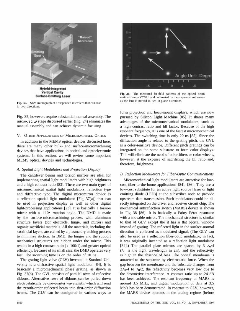
Fig. 35. SEM micrograph of a suspended microlens that can scanin two directions.
Fig. 35, however, require substantial manual assembly. Themicro- stage discussed earlier (Fig. 24) eliminates themanual assembly and can achieve dynamic focusing.
V. OTHER APPLICATIONS OFMICROMACHINED OPTICS
In addition to the MEMS optical devices discussed here,there are many other bulk- and surface-micromachiningdevices that have applications in optical and optoelectronicsystems. In this section, we will review some importantMEMS optical devices and technologies.
A. Spatial Light Modulators and Projection Display
The cantilever beams and torsion mirrors are ideal forimplementing spatial light modulators with high brightnessand a high contrast ratio [83]. There are two main types ofmicromechanical spatial light modulators: reflection typeand diffractive type. The digital micromirror device isa reflection spatial light modulator [Fig. 37(a)] that canbe used in projection display as well as other digitallight-processing applications [23]. It is basically a torsionmirror with a 10 rotation angle. The DMD is madeby the surface-micromachining process with aluminumstructure layers (for electrode, hinge, and mirror) andorganic sacrificial materials. All the materials, including thesacrificial layers, are etched by a plasma dry etching processto minimize stiction. In DMD, the hinges and the supportmechanical structures are hidden under the mirror. Thisresults in a high contrast ratio (100:1) and greater opticalefficiency. Because of its small size, the DMD operates veryfast. The switching time is on the order of 10s.
The grating light valve (GLV) invented at Stanford Uni-versity is a diffractive spatial light modulator [84]. It isbasically a micromechanical phase grating, as shown inFig. 37(b). The GVL consists of parallel rows of reflectiveribbons. Alternative rows of ribbons can be pulled downelectrostatically by one-quarter wavelength, which will sendthe zeroth-order reflected beam into first-order diffractionbeams. The GLV can be configured in various ways to
Fig. 36. The measured far-field patterns of the optical beamemitted from a VCSEL and collimated by the suspended microlensas the lens is moved in two in-plane directions.
form projection and head-mount displays, which are nowpursued by Silicon Light Machine [85]. It shares manyadvantages of the micromechanical modulators, such asa high contrast ratio and fill factor. Because of the highresonant frequency, it is one of the fastest micromechanicaldevices. The switching time is only 20 ns [85]. Since thediffraction angle is related to the grating pitch, the GVLis a color-sensitive device. Different pitch gratings can beintegrated on the same substrate to form color displays.This will eliminate the need of color filters or color wheels,however, at the expense of sacrificing the fill ratio and,therefore, brightness.
B. Reflection Modulators for Fiber-Optic Communications
Micromechanical light modulators are attractive for low-cost fiber-to-the-home applications [84], [86]. They are alow-cost substitute for an active light source [laser or lightemitting diode (LED)] at the subscriber node to provideupstream data transmission. Such modulators could be di-rectly integrated on the driver and receiver circuit chip. Themechanical antireflection switch (MARS) device is shownin Fig. 38 [86]. It is basically a Fabry–Perot resonatorwith a movable mirror. The mechanical structure is similarto that of GLV except the it has a flat optical windowinstead of grating. The reflected light in the surface-normaldirection is collected as modulated signal. (The GLV canalso be used as a reflection fiber-optic modulator; in fact,it was originally invented as a reflection light modulator[84].) The parallel plate mirrors are spaced by 3/4( is the light wavelength in air), and the reflectivityis high in the absence of bias. The optical membrane isattracted to the substrate by electrostatic force. When thegap between the membrane and the substrate changes from3 /4 to /2, the reflectivity becomes very low due tothe destructive interference. A contrast ratio up to 24 dBhas been achieved. The resonant frequency of MARS isaround 3.5 MHz, and digital modulation of data at 3.5Mb/s has been demonstrated. In contrast to GLV, however,the MARS device operates in the analog regime (before
1850 PROCEEDINGS OF THE IEEE, VOL. 85, NO. 11, NOVEMBER 1997
(a)
(b)
Fig. 37. Schematic of the (a) DMD [84] and (b) GLV [85] for display applications.
the membrane is “pulled in” toward the substrate), andthe mirror plate never makes contact with the substrate.It may have higher reliability because the probability ofstiction during operation is much reduced. A similar devicehas also been reported by researchers from the Universityof Neuchatel and Ascom [87], [88]. In their device, theyuse polysilicon membrane as a semitransparent mirror. Aphotodetector is attached to the modulator to detect thetransmitted light (the fiber collects the reflected light). Thus,a full transceiver is realized by this device potentially atvery low cost.
C. Optical Scanners
Optical scanning is another fruitful area in which opticalMEMS could play a significant role. Many different typesof microoptomechanical scanners have been proposed anddemonstrated. Most of the scanners are driven at resonantfrequency to increase the scanning angle and reduce thedriving voltage. Goto reported a two-dimensional opti-cal beam scanner using a single mirror with leaf spring
mirror resonator and piezoelectric actuator [89]. By excit-ing both the bending mode and the torsion mode of thespring leaf-connected resonator, two-dimensional scanningis achieved. A two-dimensional scanning display that com-bines a seven-element fan-shaped laser array and a surface-micromachined polysilicon microscanner was reported bythe Berkeley group (Fig. 39) [90]. The vertical scanningis achieved by simply modulating the individual lasers inthe laser array, while the horizontal scanning is achievedby the micromechanical scanner. The microscanner itselfis realized by an out-of-plane torsion mirror driven bya comb actuator through microhinges. A resolution of310 pixels/line has been achieved. A diffraction gratingscanner based on the surface-micromachined micromotor isreported by Mehregany and Merat [34]. Motamediet al. ofRockwell reported a micromechanical optical scanner basedon bimorph microactuators. A scanning angle of 20andscan range up to 2 kHz have been achieved with a powerless than 1 W [91]. Electromagnetic scanning mirrors havealso been reported [92], [93].
WU: MICROMACHINING 1851
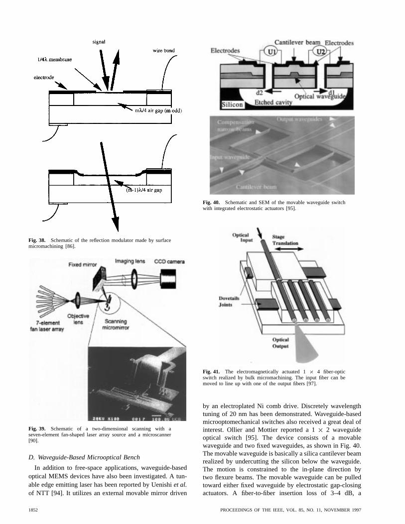
Fig. 38. Schematic of the reflection modulator made by surfacemicromachining [86].
Fig. 39. Schematic of a two-dimensional scanning with aseven-element fan-shaped laser array source and a microscanner[90].
D. Waveguide-Based Microoptical Bench
In addition to free-space applications, waveguide-basedoptical MEMS devices have also been investigated. A tun-able edge emitting laser has been reported by Uenishiet al.of NTT [94]. It utilizes an external movable mirror driven
Fig. 40. Schematic and SEM of the movable waveguide switchwith integrated electrostatic actuators [95].
Fig. 41. The electromagnetically actuated 1� 4 fiber-opticswitch realized by bulk micromachining. The input fiber can bemoved to line up with one of the output fibers [97].
by an electroplated Ni comb drive. Discretely wavelengthtuning of 20 nm has been demonstrated. Waveguide-basedmicrooptomechanical switches also received a great deal ofinterest. Ollier and Mottier reported a 1 2 waveguideoptical switch [95]. The device consists of a movablewaveguide and two fixed waveguides, as shown in Fig. 40.The movable waveguide is basically a silica cantilever beamrealized by undercutting the silicon below the waveguide.The motion is constrained to the in-plane direction bytwo flexure beams. The movable waveguide can be pulledtoward either fixed waveguide by electrostatic gap-closingactuators. A fiber-to-fiber insertion loss of 3–4 dB, a
1852 PROCEEDINGS OF THE IEEE, VOL. 85, NO. 11, NOVEMBER 1997
(a)
(b)
Fig. 42. Schematic of broadly tunable VCSEL’s with movable micromechanical top mirrors [102],[103].
switching time of 0.8 ms, and a driving voltage of28V has been obtained.
Another type of fiber-optic switch involves physicalmovement of the fiber itself instead of a waveguide. Fieldet al. of Hewlett-Packard [96] reported a 1 2 fiber-opticswitch that utilizes an electroplated (LIGA) thermal actuatorto move the input fiber between two output fibers. Acoupling loss of 5.8 dB and isolation of 66.5 dB have beenachieved. Another interesting moving-fiber-optical switch isreported by Gonzales and Collins [97]. The 14 switch(Fig. 41) consists of one movable fiber and four fixed fibers.The movable fiber is mounted on a bulk-micromachinedtranslation stage, which is actuated by an electromagneticactuator. A thin film of paramagnetic material (permalloy)is deposited on the input translation stage, and an externalmagnetic field is applied to either side of the sliding stageto align the input fiber to the appropriate output fiber. Aswitching time of 5 ms, an insertion of 1 dB, and a crosstalk of 60 dB have been achieved for multimode fibers.One of the major constraints of the waveguide-based fiber-optic switches is that they are mainly constrained to 1
switches, and it is more difficult to scale up to largerswitches.
E. Micromachined Device on III–V Substrates
Micromachining on III–V materials is a new area thathas caught a great deal of interest recently [98]–[101]. Theobvious advantage of the III–V substrate is that active opto-electronic devices such as semiconductor lasers, LED’s, andphotodetectors can be readily integrated with the microme-
chanical structure. The MEMS technology enables broadlytunable VCSEL’s, LED’s, photodetectors, and filters to beimplemented on III–V compound semiconductor substrates[102]–[106]. Basically, the wavelength tuning range of aFabry–Perot cavity with length and refractive indexcan be expressed as
where is the longitudinal mode number. Vertical-cavitylasers can have very large tuning range thanks to thewide mode spacing; however, the effect of index changedue to electrooptic or free carrier effect is very weakbecause of the small cavity length ( 5 m). On theother hand, a very broad tuning range can be obtainedby changing the cavity length. This can be accomplishedby employing a movable mirror for the cavity. Indeed,a very broad tuning range ( 20 nm) has been demon-strated in such micromachined VCSEL’s. Two types ofmovable mirrors have been investigated: one employs a de-formable metal/dielectric/semiconductor membrane [102],the other uses single crystalline semiconductor cantileverbeams [103], as shown in Fig. 42(a) and (b), respectively.Broadly tunable LED’s, photodetectors, and filters at longwavelength have also been demonstrated [104].
VI. CONCLUSION
The micromachining technology has opened up manynew possibilities for optical and optoelectronic systems.It allows movable micromechanical structures to be inte-
WU: MICROMACHINING 1853

grated monolithically with microoptical elements. The inte-grated micromechanical device can perform many functionsthat are not achievable with conventional devices. Opticalswitches with low loss and high isolation, optical scan-ners with large scanning angles, high-brightness projectiondisplays, low-cost fiber-optic modulators, broadly tunablesemiconductor lasers, photodetectors, and filters have beendemonstrated. Single-chip microoptical systems have alsobeen built. Compared with conventional optomechanicaldevices, the microfabricated devices are smaller, lighter,cheaper, faster, and more rugged and consume less power.
ACKNOWLEDGMENT
The author wishes to thank Dr. L.-Y. Lin of AT&TResearch Labs, Dr. J.-L. Shen, L. Fan, S.-S. Lee, C. R.King, J. G. D. Su, and R. Chen for the research workdone at UCLA; Prof. K. S. J. Pister for valuable discus-sions on microhinges; Prof. W. Kaiser, Prof. C. J. Kim,and Dr. M. E. Motamedi for stimulating discussions; theMicroelectronics Center at North Carolina for fabricationof the surface-micromachined devices; and members of theNanofabrication Research Facility at UCLA for help infabricating the devices.
REFERENCES
[1] S. E. Miller, “Integrated optics: An introduction,”Bell Syst.Tech. J.,vol. 48, pp. 2059–2068, 1969.
[2] For an overview, see W. S. Trimmer,Micromechanics andMEMS—Classic and Seminal Papers to 1990.Piscataway, NJ:IEEE Press, 1997.
[3] For an overview of the recent development in optical MEMS,seeDig. IEEE/LEOS 1996 Summer Topical Meeting on OpticalMEMS and Their Applications,IEEE, Piscataway, NJ, 1996.
[4] See “Special issue on micro-opto-electro-mechanical systems,”Opt. Eng.,vol. 36, pp. 1280–1413, May 1997.
[5] K. E. Petersen, “Silicon as a mechanical material,”Proc. IEEE,vol. 70, pp. 420–457, 1982.
[6] K. E. Bean, “Anisotropic etching of silicon,”IEEE Trans.Electron Devices,vol. ED-25, pp. 1185–1193, Oct. 1978.
[7] C. H. Henry, G. E. Blonder, and R. F. Kazarinov, “Glasswaveguides on silicon for optical packaging,”J. LightwaveTechnol.,vol. 7, pp. 1530–1539, Oct. 1989..
[8] H. Han, J. E. Schramm, J. Mathews, and R. A. Boudreau,“Micromachined silicon structures for single mode passivealignment,” inProc. SPIE Optoelectronic Packaging,vol. 2691,pp. 118–123, Feb. 1996.
[9] Y. Uenishi, M. Tsugai, and M. Mehregany, “Micro-opto-mechanical devices fabricated by anisotropic etching of (110)silicon,” J. Micromech. Microeng.,vol. 5, pp. 305–312, Dec.1995.
[10] K.-S. Seo, Y.-H. Cho, and S.-K. Youn, “An electrostatically-tunable switching micromirror using (110) silicon wafers,” inDig. IEEE/LEOS 1996 Summer Topical Meetings on OpticalMEM’s and Their Applications,Keystone, CO, 1996, pp. 41–42.
[11] S. Kong, K. Minami, and M. Esashi, “Fabrication of reactiveion etching systems for deep silicon machining,”Trans. Inst.Electr. Eng. Jpn. E,vol. 117-E, pp. 10–14, Jan. 1997.
[12] E. H. Klaassen, K. Petersen, J. M. Noworolski, J. Logan,N. I. Maluf, J. Brown, C. Storment, W. McCulley, and G.T. A. Kovacs, “Silicon fusion bonding and deep reactive ionetching: A new technology for microstructures,”Sens. ActuatorsA (Physical),vol. A52, pp. 132–139, Mar./Apr. 1996.
[13] C. Marxer, M.-A. Gretillat, N. F. de Rooij, R. Battig, O.Anthamatten, B. Valk, and P. Vogel, “Vertical mirrors fabricatedby reactive ion etching for fiber optical switching applications,”in Proc. 10th Workshop Micro Electro Mechanical Systems(MEMS), Nagoya, Japan, 1997, pp. 49–54.
[14] W. H. Juan and S. W. Pang, “Batch-micromachined, high aspectratio Si mirror arrays for optical switching applications,” in
Proc. Int. Conf. Solid-State Sensors and Actuators (TRANS-DUCERS ’97),1997, paper 1A4.09P.
[15] H. C. Nathanson, W. E. Newell, R. A. Wickstrom, and J. R.Davis, Jr., “The resonant gate transistor,”IEEE Trans. ElectronDevices,vol. ED-14, pp. 117–133, 1967.
[16] R. T. Howe and R. S. Muller, “Polycrystalline silicon microme-chanical beams,”J. Electrochem. Soc.,vol. 130, pp. 1420–1423,1983.
[17] M. Mehregany, K. J. Gabriel, and W. S. N. Trimmer, “In-tegrated fabrication of polysilicon mechanisms,”IEEE Trans.Electron Devices,vol. 35, pp. 719–723, 1988.
[18] L. S. Fan, Y. C. Tai, and R. S. Muller, “Integrated movablemicromechanical structures for sensors and actuators,”IEEETrans. Electron Devices,vol. 35, pp. 724–730, 1988.
[19] , “IC-processed electrostatic micro-motors,” inProc. IEEEInt. Electronic Device Meeting (IEDM),San Francisco, CA,1988, pp. 666–669.
[20] Y. C. Tai, L. S. Fan, and R. S. Muller, “IC-processed micro-motors: Design, technology, and testing,” inProc. IEEE MicroElectro Mechanical Systems (MEMS),Salt Lake City, UT, 1989,pp. 1–6.
[21] J. H. Smith, S. Montague, J. J. Sniegowski, J. R. Murray,and P. J. McWhorter, “Embedded micromechanical devices forthe monolithic integration of MEMS with CMOS,” inProc.Int. Electron Devices Meeting,Washington, D.C., 1995, pp.609–612.
[22] M. Fischer, M. Nagele, D. Eichner, C. Schollhorn, and R. Stro-bel, “Integration of surface-micromachined polysilicon mirrorsand a standard CMOS process,”Sens. Actuators A (Physical),vol. A52, pp. 140–144, 1996.
[23] L. J. Hornbeck, “Digital light processing and MEMS: Timelyconvergence for a bright future” (abstract), inProc. SPIE Symp.Micromachining and Microfabrication,Austin, TX, Oct. 1995.
[24] K. S. J. Pister, M. W. Judy, S. R. Burgett, and R. S. Fear-ing, “Microfabricated hinges,”Sens. Actuators A,vol. 33, pp.249–256, 1992.
[25] Y. Fukuta, D. Collard, T. Akiyama, E. H. Yang, and H. Fujita,“Microactuated self-assembling of 3D polysilicon structureswith reshaping technology,” inProc. IEEE Micro Electro Me-chanical Systems (MEMS),Nagoya, Japan, 1977, pp. 477–481.
[26] P. W. Green, R. R. A. Syms, and E. M. Yeatman, “Demon-stration of three-dimensional microstructure self-assembly,”J.Microelectromech. Syst.,vol. 4, pp. 170–176, 1995.
[27] E. Smela, L. Inganas, and I. Lundstrom, “Controlled folding ofmicrometer-size structures,”Science,vol. 268, pp. 1735–1738.
[28] M. C. Wu, L. Y. Lin, S. S. Lee, and K. S. J. Pister, “Micro-machined free-space integrated micro-optics,”Sens. Actuators:A (Physical),vol. 50, pp. 127–134, 1995.
[29] M. E. Motamedi, M. P. Griswold, and R. E. Knowlden, “Siliconmicrolenses for enhanced optical coupling to silicon focalplanes,” inProc. SPIE,vol. 1544, 1991, pp. 22–32.
[30] K. Rastani, A. Marrakchi, S. F. Habiby, W. M. Hubbard, H.Gilchrist, and R. E. Nahory, “Binary phase Fresnel lenses forgeneration of two-dimensional beam arrays,”Appl. Opt.,vol.30, no. 11, pp. 1347–1354, 1991.
[31] M. E. Motamedi, M. C. Wu, and K. S. J. Pister, “Micro-opto-mechanical devices and on-chip optical processing,”Opt. Eng.,vol. 36, pp. 1282–1297, 1997.
[32] L. Y. Lin, S. S. Lee, K. S. J. Pister, and M. C. Wu, “Three-dimensional micro-Fresnel optical elements fabricated by mi-cromachining technique,”Electron. Lett.,vol. 30, pp. 448–449,1994.
[33] , “Micro-machined three-dimensional micro-optics for in-tegrated free-space optical system,”IEEE Photon. Technol.Lett., vol. 6, pp. 1445–1447, 1994.
[34] A. A. Yasseen, S. W. Smith, M. Mehregany, and F. L. Merat,“Diffraction grating scanners using polisilicon micromotors,”in Proc. IEEE Micro Electro Mechanical Systems,Amsterdam,The Netherlands, Jan. 29–Feb. 2, 1995, pp. 175–180.
[35] H. Sankur, E. Motamedi, R. Hall, W. J. Gunning, and M.Khoshnevisan, “Fabrication of refractive microlens arrays,” inProc. SPIE Micro-Optics/Micromechanics and Laser Scanningand Shaping,vol. 2383, 1995, pp. 179–183.
[36] T. R. Jay, M. B. Stern, and R. E. Knowlden, “Effect of refractivemicrolens array fabrication parameters on optical quality,” inProc. SPIE Miniature and Micro-Optics,vol. 1751, 1992, pp.236–245.
[37] Z. D. Popovic, R. A. Sprague, and G. A. Neville Connell,
1854 PROCEEDINGS OF THE IEEE, VOL. 85, NO. 11, NOVEMBER 1997
“Technique for monolithic fabrication of microlens arrays,”Appl. Opt.,vol. 27, no. 7, pp. 1281–1284, 1988.
[38] N. J. Phillips and C. A. Barnett, “Micro-optic studies usingphotopolymers,” inProc. SPIE Miniature and Micro-Optics,vol. 1544, 1991, pp. 10–21.
[39] C. R. King, L. Y. Lin, and M. C. Wu, “Monolithically integratedrefractive microlens standing perpendicular to the substrate,” inProc. SPIE Photonics West’96,San Jose, CA, Jan. 1996, vol.2687, pp. 123–130.
[40] P. Beckmann and A. Spizzichino,The Scattering of Electro-magnetic Waves From Rough Surface.Norwood, MA: ArtechHouse, 1987, ch. 3–5.
[41] S. S. Lee, L. Y. Lin, and M. C. Wu, “Surface-micromachinedfree-space micro-optical systems containing three-dimensionalmicro-gratings,” Appl. Phys. Lett.,vol. 67, pp. 2135–2137,1995.
[42] , “Distributed feedback lasers integrated with microma-chined wavelength-meter for dense WDM systems,” inProc.1996 Conf. Lasers and Electro-Optics (CLEO),Anaheim, CA,June 3–7, 1996, paper CFG2.
[43] M. H. Kiang, J. T. Nee, K. Y. Lau, and R. S. Muller, “Surface-micromachined diffraction gratings for scanning spectroscopicapplications,” inProc. Int. Conf. Solid-State Sensors and Actu-ators (TRANSDUCERS ’97),1997, pp. 343–345.
[44] W. C. Tang, T. C. H. Nguyen, and R. T. Howe, “Laterally drivenpolysilicon resonant microstructures,” inProc. Micro ElectroMechanical Systems (MEMS),1989, pp. 53–59.
[45] W. C. Tang, T. C. H. Nguyen, M. W. Judy, and R. T. Howe,“Electrostatic-comb drive of lateral polysilicon resonators,”Sensors Actuators A (Physical), vol. A21, pp. 328–331, 1990.
[46] M. T. Ching, R. A. Brennen, and R. M. White, “Microfabricatedoptical chopper,” inProc. SPIE,1993, vol. 1992, pp. 40–46.
[47] M. H. Kiang, O. Solgaard, R. S. Muller, and K. Lau, “Micro-machined polysilicon microscanners for barcode readers,”IEEEPhoton. Technol. Lett.,vol. 8, pp. 1707–1709, 1996.
[48] W. S. N. Trimmer and K. J. Gabriel, “Design considerationsfor a practical electrostatic micro-motor,”Sens. Actuators,vol.11, pp. 189–206, 1987.
[49] P. B. Chu, P. R. Nelson, M. I. Tachiki, and K. S. J. Pister,“Dynamics of polysilicon parallel-plate electrostatic actuators,”Sens. Actuators A (Physical),vol. A52, p. 216–220, 1996.
[50] A. P. Lee and A. P. Pisano, “Polysilicon angular microvibro-motors,” J. Microelectromech. Syst.,vol. 1, pp. 70–76, 1992.
[51] M. M. Daneman, N. C. Tien, O. Solgaard, A. P. Pisano, K. Y.Lau, and R. S. Muller, “Linear microvibromotor for positioningoptical components,”J. Microelectromech. Syst.,vol. 5, pp.159–165, 1996.
[52] M. J. Daneman, O. Solgaard, N. C. Tien, K. Y. Lau, and R. S.Muller, “Laser-to-fiber coupling module using a micromachinedalignment mirror,” IEEE Photon. Technol. Lett.,vol. 8, pp.396–398, 1996.
[53] R. Yeh, E. J. J. Kruglick, and K. S. J. Pister, “Surface-micromachined components for articulated microrobots,”J.Microelectromech. Syst.,vol. 5, pp. 10–17, 1996.
[54] N. R. Tas, A. H. Sonnenberg, A. F. M. Sander, and M. C.Elwenspoek, “Surface micromachined linear electrostatic step-per motor,” in Proc. IEEE Micro Electro Mechanical Systems(MEMS), 1997, pp. 215–220.
[55] E. J. Garcia and J. J. Sniegowski, “Surface micromachinedmicroengine,” Sens. Actuators A (Physical),vol. A48, pp.203–214, 1995.
[56] J. J. Sniegowski and E. J. Garcia, “Surface-micromachined geartrains driven by an on-chip electrostatic microengine,”IEEEElectron Device Lett.,vol. 17, pp. 366–368, 1996.
[57] J. J. Sniegowski, S. L. Miller, G. F. LaVigne, M. S. Rodgers,and P. J. McWhorter, “Monolithic geared-mechanisms drivenby a polysilicon surface-micromachined on-chip electrostaticmicroengine,” inProc. Solid State Sensor and Actuator Work-shop,Hilton Head, SC, 1996, pp. 178–182.
[58] J. J. Sniegowski and E. J. Garcia, “Microfabricated actuatorsand their application to optics,” inProc. SPIE,vol. 2383, 1995,pp. 46–64.
[59] T. Akiyama and K. Shono, “Controlled stepwise motion inpolysilicon microstructures,”J. Microelectromech. Syst.,vol. 2,pp. 106–110, 1993.
[60] T. Akiyama, D. Collard, and H. Fujita, “Scratch drive actuatorwith mechanical links for self-assembly of three-dimensionalMEMS,” J. Microelectromech. Syst.,vol. 6, pp. 10–17, 1997.
[61] P. Langlet, D. Collard, T. Akiyama, and J. Fujita, “A quanti-tative analysis of scratch drive actuation for integratedmotion system,” inProc. Int. Conf. Solid-State Sensors andActuators (TRANSDUCERS 97),1997, paper 3A2.01.
[62] L. Fan, M. C. Wu, K. Choquette, and M. H. Crawford, “Self-assembled microactuated stages for optical scanning andalignment,” in Proc. 1997 Int. Conf. Solid-State Sensors andActuators (TRANSDUCERS 97),1997, paper 2A2.01.
[63] S. S. Lee, E. Motamedi, and M. C. Wu, “Surface-micromachined free-space fiber optic switches with integratedmicroactuators for optical fiber communication systems,”in Proc. 1997 Int. Conf. Solid-State Sensors and Actuators(TRANSDUCERS 97),1997, paper 1A4.07P.
[64] G. D. Su, L. Y. Lin, and M. C. Wu, “Single-chip femtosecondautocorrelator realized by surface-micromachined integratedoptics,” in Proc. Conf. Lasers and Electro-Optics (CLEO),Baltimore, MD, 1997, paper CWL2.
[65] H. Guckel, J. Klein, T. Christenson, K. Skrobis, M. Laudon,and E. G. Lovell, “Thermalmagnetic metal flexure actuators,” inProc. IEEE Solid State Sensors and Actuators Workshop,HiltonHead, SC, 1992, p. 73.
[66] J. H. Comtois, V. M. Bright, and M. W. Phipps, “Thermalmicroactuators for surface-micromachining processes,” inProc.SPIE, 1995, vol. 2642, pp. 10–21.
[67] J. H. Comtois and V. M. Bright, “Applications for surface-micromachined polysilicon thermal actuators and arrays,”Sens.Actuators A (Physical),vol. A58, pp. 19–25, 1997.
[68] L. Y. Lin, S. S. Lee, and M. C. Wu, “45� out of plane beamsteering optics for vertical alignment in free-space micro-opticalbench,” in Proc. Conf. Lasers and Electro-Optics (CLEO),Anaheim, CA, 1996, paper CFC5.
[69] L. Y. Lin, J. L. Shen, S. S. Lee, and M. C. Wu, “Surface-micromachined micro- stages for free-space micro-opticalbench,”IEEE Photon. Technol. Lett.,vol. 9, pp. 345–347, Mar.1997.
[70] Y. Xu, N. C. MacDonald, and S. A. Miller, “Integrated micro-scanning tunneling microscope,”Appl. Phys. Lett.,vol. 67, pp.2305–2307, 1995.
[71] A. Selvakumar, K. Najafi, W. H. Juan, and S. Peng, “Ver-tical comb array microactuators,” inProc. IEEE WorkshopMicro Electro Mechanical Systems,Amsterdam, The Nether-lands, 1995, pp. 43–48.
[72] L. Fan and M. C. Wu, “Self-assembled micro-XYZ stagesfor moving micro-ball lenses,” presented at the Int. Conf. onOptical MEMS and Their Applications, Nara, Japan, Nov.1997.
[73] L. Y. Lin, J. L. Shen, S. S. Lee, and M. C. Wu, “Realizationof novel monolithic free-space optical disk pickup heads bysurface micromachining,”Opt. Lett.,vol. 21, no. 2, pp. 155–157,Jan. 15, 1996.
[74] M. F. Dautartas, A. M. Benzoni, Y. C. Chen, G. E. Blonder, B.H. Johnson, C. R. Paola, E. Rice, and Y. H. Wong, “A silicon-based moving mirror optical switch,”J. Lightwave Technol.,vol. 8, pp. 1078–1085, 1992.
[75] S. S. Lee, L. Y. Lin, and M. C. Wu, “Surface-micromachinedfree-space fiber optic switches,”Electron. Lett.,vol. 31, no. 17,pp. 1481–1482, Aug. 1995.
[76] W. S. N. Trimmer, “Microrobots and micromechanical sys-tems,” Sens. Actuators,vol. 19, pp. 267–287, 1989.
[77] H. Toshiyoshi and H. Fujita, “Electrostatic micro torsion mirrorsfor an optical switch matrix,”J. Microelectromech. Syst.,vol.5, pp. 231–237, 1996.
[78] R. A. Miller, Y. C. Tai, G. Xu, J. Bartha, and F. Lin, “An elec-tromagnetic MEMS 2 2 fiber optic bypass switch,” inProc.Int. Conf. Solid-State Sensors and Actuators (TRANSDUCERS’97), 1997, pp. 89–92.
[79] E. Hashimoto, Y. Uenishi, K. Honma, and S. Nagaoka, “Micro-optical gate for fiber optic communications,” inProc. Int. Conf.Solid-State Sensors and Actuators (TRANSDUCERS ’97),1997,pp. 331–334.
[80] E. M. Strzelecka, G. D. Robinson, M. G. Peters, F. H. Peters,and L. A. Coldren, “Monolithic integration of vertical-cavitylaser diodes with refractive GaAs microlenses,”Electron. Lett.,vol. 31, pp. 724–725, 1995.
[81] T. Du, M. E. Warren, J. R. Wendt, G. A. Vawter, S. P. Kilcoyne,K. L. Lear, R. P. Schneider, A. J. Howard, R. F. Carson, and J.C. Zolper, “Directional beam control using on/off-axis high-efficiency diffractive optics integrated on substrate-emitting
WU: MICROMACHINING 1855
vertical cavity lasers,” inProc. Conf. Lasers and Electro-Optics(CLEO’95), Baltimore, MD, 1995, pp. 195–196.
[82] L. Fan, M. C. Wu, and K. D. Choquette, “Two-dimensionalscanning microlenses for vertical cavity surface-emittinglasers,” in 1997 Conf. of Lasers and Electro-Optics (CLEO),Baltimore, MD, May 18–23, 1997, paper CME2.
[83] K. E. Petersen, “Silicon torsional scanning mirror,”IBM J. Res.Develop.,vol. 24, pp. 631–637, 1980.
[84] O. Solgaard, F. S. A. Sandejas, and D. M. Bloom, “Deformablegrating optical modulator,”Opt. Lett., vol. 17, pp. 688–690,1992.
[85] D. M. Bloom, “The grating light valve: Revolutionizing displaytechnology,” inProc. SPIE,1997.
[86] J. A. Walker, K. W. Goossen, and S. C. Arney, “Fabrication of amechanical antireflection switch for fiber-to-the-home systems,”J. Microelectromech. Syst.,vol. 5, pp. 45–51, 1996.
[87] C. Marxer, M. A. Gretillat, V. P. Jaecklin, R. Baettig, O.Anthamatten, P. Vogel, and N. F. de Rooij, “Megahertz opto-mechanical modulator,”Sens. Actuators A (Physical),vol. A52,pp. 46–50, 1996.
[88] O. Anthamatten, R. K. Battig, B. Valk, P. Vogel, C. Marxer,M. Gretillat, and N. F. de Rooij, “Packaging of a reflectiveoptical duplexer based on silicon micromechanics,” inProc.IEEE/LEOS 1996 Summer Topical Meetings on Optical MEM’sand Their Applications,Piscataway, NJ, 1996, pp. 61–62.
[89] H. Goto, “Si micromachined 2D optical scanning mirror andits application to scanning sensors,” inProc. IEEE/LEOS 1996Summer Topical Meetings on Optical MEM’s and Their Appli-cations,,Piscataway, NJ, 1996, pp. 17–18.
[90] D. A. Francis, M.-H. Kiang, O. Solgaard, K. Y. Lau, R. S.Muller, and C. J. Chang-Hasnain, “Compact 2D laser beamscanner with fan laser array and Si micromachined microscan-ner,” Electron. Lett.,vol. 33, pp. 1143–1145, 1997.
[91] M. E. Motamedi, S. Park, A. Wang, M. S. Dadkhah, A. P.Andrews, H. O. Marcy, M. Khoshnevisan, A. E. Chiou, R. J.Huhn, C. F. Sell, and J. G. Smits, “Development of micro-electro-mechanical optical scanner,”Opt. Eng., vol. 36, pp.1346–1353, 1997.
[92] R. A. Miller and T. Yu-Chong, “Micromachined electromag-netic scanning mirrors,”Opt. Eng., vol. 36, pp. 1399–1407,1997.
[93] J. W. Judy, R. S. Muller, and H. H. Zappe, “Magnetic microac-tuation of polysilicon flexure structures,”J. Microelectromech.Syst.,vol. 4, pp. 162–169, 1995.
[94] Y. Uenishi, K. Honma, and S. Nagaoka, “Tunable laser diodeusing a nickel micromachined external mirror,”Electron. Lett.,vol. 32, no. 13, pp. 1207–1208, June 20, 1996.
[95] E. Ollier and P. Mottier, “Integrated electrostatic micro-switchfor optical fiber networks driven by low voltage,”Electron.Lett., vol. 32, pp. 2007–2009, 1996.
[96] L. A. Field, D. L. Burriesci, P. R. Robrish, and R. C. Ruby,“Micromachined 1*2 optical-fiber switch,”Sens. Actuators A(Physical),vol. A53, pp. 311–316, 1996.
[97] C. Gonzalez and S. D. Collins, “Magnetically actuated fiber-optic switch with micromachined positioning stages,”Opt. Lett.,vol. 22, pp. 709–711, 1997.
[98] Z. L. Zhang and N. C. MacDonald, “Fabrication of submicronhigh-aspect-ratio GaAs actuators,”J. Microelectromech. Syst.,vol. 2, pp. 66–73, 1993.
[99] K. Hjort, J. Soderkvist, and J.-A. Schweitz, “Gallium arsenideas a mechanical material,”J. Micromech. Microeng.,vol. 4, pp.1–13, 1994.
[100] Y. Uenishi, H. Tanaka, and H. Ukita, “Characterization ofAlGaAs microstructure fabricated by AlGaAs/GaAs microma-chining,” IEEE Trans. Electron Devices,vol. 41, pp. 1778–1783,Oct. 1994.
[101] K. Hjort, “Sacrificial etching of III–V compounds for mi-cromechanical devices,”J. Micromech. Microeng.,vol. 6, pp.370–375, 1996.
[102] F. Sugihwo, M. C. Larson, J. S. Harris, Jr., “Low thresholdcontinuously tunable vertical-cavity surface-emitting lasers with19.1 nm wavelength range,”Appl. Phys. Lett.,vol. 70, pp.547–549, 1997.
[103] M. Y. Li, W. Yuen, G. S. Li, and C. J. Chang-Hasnain, “Highperformance continuously tunable top-emitting vertical cavitylaser with 20 nm wavelength range,”Electron. Lett.,vol. 33,pp. 1051–1052, 1997.
[104] G. L. Christenson, A. T. T. D. Tran, Z. H. Zhu, Y. H. Lo, M.Hong, J. P. Mannaerts, and R. Bhat, “Long-wavelength resonantvertical-cavity LED/photodetector with a 75-nm tuning range,”IEEE Photon. Technol. Lett.,vol. 9, pp. 725–727, 1997.
[105] E. C. Vail, M. S. Wu, G. S. Li, L. Eng, and C. J. Chang-Hasnain, “GaAs micromachined widely tunable Fabry–P´erotfilters,” Electron. Lett.,vol. 31, pp. 228–229, 1995.
[106] M. C. Larson and J. S. Harris, Jr., “Broadly-tunable resonant-cavity light-emitting diode,”IEEE Photon. Technol. Lett.,vol.7, pp. 1267–1269, 1995.
Ming C. Wu (Member, IEEE) received the M.S.and Ph.D. degrees in electrical engineering fromthe University of California, Berkeley, in 1985and 1988, respectively.
From 1988 to 1992, he was a member ofthe Technical Staff at AT&T Bell Laboratories,Murray Hill, NJ, where he conducted researchin high-speed semiconductor lasers and opto-electronics. In 1993, he joined the Faculty ofthe Electrical Engineering Department of theUniversity of California, Los Angeles, where he
currently is a Professor. He also is the Director of the MURI Center onRF Photonic Materials and Devices sponsored by the Office of Naval Re-search. His current research interests include micromachined microoptics,optical microelectromechanical systems (MEMS), free-space integratedoptics, ultrafast integrated optoelectronics, microwave photonics, high-power photodetectors, semiconductor lasers, and optical interconnect. Hehas published more than 85 journal papers, 120 conference papers, andone book chapter, and has received eight U.S. patents.
Dr. Wu is a member of the American Physical Society, the OpticalSociety of America, the International Union of Radio Science, and EtaKappa Nu. He was General Cochair of the IEEE LEOS Summer TopicalMeeting in 1995 (RF Optoelectronics) and 1996 (Optical MEMS) andProgram Committee Chair of the 1997 IEEE LEOS Topical Meetingon Optical MEMS. He also served on the Program Committee of theConference on Lasers and Electro-Optics from 1996 to 1998 and IEDMin 1996. He received the Packard Foundation Fellowship in 1992 and theMeritorious Conference Paper Award of the 1994 Government Microcir-cuit Applications Conference.
1856 PROCEEDINGS OF THE IEEE, VOL. 85, NO. 11, NOVEMBER 1997