
Micromachining f MEMS f or MEMS f g Technologies f b i ti abrication
77
Micromachining Micromachining f MEMS f for MEMS f Carmen M Carmen M g Technologies g Technologies fbi ti fabrication Moldovan Moldovan
Transcript of Micromachining f MEMS f or MEMS f g Technologies f b i ti abrication

MicromachiningMicromachining
f MEMS ffor MEMS f
Carmen MCarmen M
g Technologiesg Technologies
f b i tifabrication
MoldovanMoldovan

SILICON MICROMACHININGSILICON MICROMACHINING
• INTRODUCTION
•BULK MICROMACHINING
•SURFACE MICROMACHINING
POLYMER MICROMACHINING
GLASS MICROMACHINING
CERAMICS MICROMACHININGCERAMICS MICROMACHINING
G
GG

INTRODUCTIONSILICON as a material for MST/MEMS
Positive:
• Good electrical and mechanical propert
W ll d t d h t i ti• Well understood characteristics
• Well established processing methods
• Integration of mechanical/electronic/opti
Limitations:Limitations:
•Limited materials flexibility e.g no magne
•Difficult interfacing - interconnections/ p
•Limited functionality at high temperature
ties e.g. elasticity, piezoresistivity
cal functions
etic material, no piezoelectric
packaging problems still under development

MICROMACHINING TECHNOLOG•Micromachining technology allows the fabri•Micromachining technology allows the fabristructures with very small dimensions (in thprocesses, different of conventional IC tech
•Generally the micromachining technology cand surface micromachining
B lk i hi i i b d i l– Bulk micromachining is based on single cmicromechanical structures developed wsilicon crystal or deposited or grown laye
Mi h i l t t d d b•Micromechanical structures produced by minto three groups: static, dynamic, and kinem
• Static micromechanical structures includes frenozzles, cavities, capillary column, circular ori
• Dinamic micromechanical structures: diaphragb t Th i t l di lbeams, resonators. They require control displa
• The kinematic group includes micromotors, msliders. The kinematic devices ar considered toand microsurgery.
Ycation of electro mechanical opticalcation of electro- mechanical optical
he micrometer range), 3D, using special nologies.
an be classified in : bulk micromachining
t l ili t hi d thcrystal silicon etching, and the with this technology are made of either ers on silicon.
i hi i t h l b di id dicromachining technology can be divided matic.
ee three dimensional structures such as ifices, miniature electrical connectors.
gmes, membranes, microbridges, cantilever t t li h th d i d f tiacement to accomplish the desired function.
icrogears, pin joints, springs, cranks, o be essential in the future for microrobotics

DIMENSIONS

Metal O ide Nanoparticles in CMetal Oxide Nanoparticles in C
BORESI AND CHONG, ELASTICITY IN ENGIN
CoatingsCoatings
NEERING MECHANICS, WILEY, 2000.

Bulk micromachining = 3D configuration technBulk micromachining = 3D configuration technprocesses: chemical and electrochemical anisolaser technique, anodic bonding, double side a
Bulk micromachining of silicon is based mainlyfact that certain aqueous alkaline solutions attavarious crystallographic directionsy g p
Silicon crystallographic directions
Crystallographic Structureis a diamond type cristal with centrated faces, and a constant lattice ,of 5,43 A
nique of silicon and thin films by using specific
Bulk micromachining technique
nique of silicon and thin films by using specific otropic etching, stop etch technique, assisted alignment, LIGA technique.
y on anisotropic etching. This relies on the ack silicon at widely differing speeds in the

Crystallographic orientation – Dy g pA basic feature of anisotropic etchants is that crystallographic planes. <111> surfaces etch aplanes This indicates that the dissolution rateplanes. This indicates that the dissolution rateof the silicon rate. Anisotropic etching is a funatoms per square centimetre), the energy needgeometric screening effects (three-dimensionag g (consequences of anisotropy it is possible to devfeasible.
EDP etch rate dependence on crystallographic orientation in <100> silicon.
Dependent Etch rateBulk micromachining technique
ptheir etch rates are dependent of the
at a slower rate than all other crystallographic e will be a function of the crystal orientatione will be a function of the crystal orientation nction of the density of atoms (number of ded to remove an atom from the surface, and al distribution of atoms in the lattice). As a )velop unique structures not otherwise
Truncated pyramidal pit boundedby silicon <111>planes

Etching profile for Silicon <100>Etching profile for Silicon <100> anisotropically etched
Bulk micromachining technique
Etching profile for Silicon <110>Etching profile for Silicon <110> anisotropically etched

Layer 1 (SiO2)
Lithographic Pro
Silicon substrate
Layer 1 (SiO2)
A. Oxidation
Negative photoresiscoat
Silicon substrate
Layer 1 (SiO2)
B. Litography preparation
UV Light
Glass Plate
Opaque Pattern
Hardened R
Layer 1 (SiO2)
Silicon substrate
C. Exposure
Negative i t
ocess Bulk micromachining technique
Silicon
Layer 1 (SiO2)resist
t
Silicon substrate
D. Unexposed Photoresist Removed by Developer
Negative resistLayer 1 (SiO2)
Silicon substrate
Resist
E. SiO2 etched with NH4F + HF
Negative resistLayer 1 (SiO )
Silicon substrate
Layer 1 (SiO2)
F. Exposed Photoresist Removed with H2SO4
SILICON BULK MIC
Anisotropic etcD bl id liDouble side aligLaser machininLaser machininAnodic Bonding
CROMACHINING
hingtgnment
ggg

SILICON ANISOTROPIC. SILICON ANISOTROPIC
Anisotropic etching of silicon waAnisotropic etching of silicon wa
•Orientation of monocrystaline silicon
•High dose boron concentration
• Etchant temperature p
•Composition and concentration of the etch
The most important anisotropic e
Hydroxides of alkaline metals: KOH NaOH LiHydroxides of alkaline metals: KOH, NaOH, Li
Diamines:EDP(Ethylenediamine-pyrocatechol-W
Tetramethylammonium Hydroxide (TMAH)
C ETCHING
Bulk micromachining technique
C ETCHING
as studied as a function of:as studied as a function of:
hant
etchants of silicon
iOH CsOHiOH, CsOH
Water)
)

KOH (potassium hydroxide) – high etch rate,the etching rate on the crystallographic orientat
ANISOTROPIC ETCHINGANISOTROPIC ETCHING
the etching rate on the crystallographic orientat
Up to now, two aspects of the silicon etching hav
a) The general reaction:a) The general reaction:
Si + 2H2O + 2HO- → SiO2(OH)22- + 2H2
b) The intrinsic etching process steps:) g p p
b1. Diffusion of the reactant molecules through
b2. Adsorption of reactant molecules on the soli
b3. Surface reaction;
b4. Reaction product desorbtion;
b5. Diffusion of by-products back across the bou
Bulk micromachining technique
strong alkaline character, high dependence oftion and boron concentration of the substrate
G OF SILICONG OF SILICON
tion and boron concentration of the substrate
ve been generally accepted /3.1/, /3.2/:
the boundary layer to the silicon surface;
id surface of silicon;
undary layer into the bulk of the solution

Potassium Hydroxide - KOH1) The highest etch rate has been obtained for a cKOH + isopropylic alcohol. The isopropylic alcohKOH isopropylic alcohol. The isopropylic alcohrate and of the boiling temperature of the solution.
2) No effect of the etchant stirring has been found ⇒
3) The ration between the etch rates of the silicon di
Seidel
Bulk micromachining technique
Hconcentration of 10 - 15% simple KOH and ~ 30%hol in KOH solution leads to the decrease of the etchhol in KOH solution leads to the decrease of the etch
⇒ the reaction is not limited by the diffusion
irections Si<100>/Si<111> is 35:1

Ethylendiamine – pyrocathecol –wat
Si etch rate in EDP, after Seidel /2.2/
Bulk micromachining technique
er (EDP)
Si etch rate in EDP – experimental/2.5/p

Ethylendiamine – pyrocathecol
The micropyramides are related to the pi t i t h t d f i tanisotropic etchants used for experiment an
Changing the composition of etchants, it isize of micropyramides
Micropyramides are the results of the aniMicropyramides are the results of the anitogether, the smallest are situated on one of edge of the pyramid base to be curved, not
-
Fig.2. 5. Silicon hillocks during th
Bulk micromachining technique
plan <111>, one characteristic of all the d t dnd study.
is possible to modified the density and the
sotropy of the solution they appearsotropy of the solution, they appear f the pyramid side, and make that the
right.
he anisotropic etching in EDP /Tan/.

AFM I ti ti f iliAFM Investigation of silicon waanisotropic etchin
b)a
Rouetchc
coma)com
f h ft th
Bulk micromachining technique
afer roughness after the ng process
ughness of a silicon wafer 200µm thickness,hed in 4.5M KOH+ redox system +
l t t 800C (3D AFM i ti ti )mplexant, at 800C (3D-AFM investigation):calix[4]arene complexant; b) ether crown
mplexant; c) simple 4.5M KOH

HILLOCKS MINIMIZATIONHILLOCKS MINIMIZATION
a) 10-2 [M/l] phenol concentration b) 10-3 [M/l] ph
Fi 2 12 T i
d)10-5 [M/l] phenol concentration
Fig.2.12. Top vieof n type<100> S4.5M KOH+ 10-4
butylphenol
Fig. 2.11. a, b, c, d Top view microscop picture of n type <100> Si etched 1h at 850C in 4.5M KOH+ phenol at different concentration
ON THE SILICON SURFACEBulk micromachining technique
ON THE SILICON SURFACE
henol concentration c) 10-4 [M/l] phenol concentration
i i tew microscop picture Si etched 1h at 850C in 4 M/l p-tert
Fig.2.13.Top view microscop picture of n type<100> Si etched 1h at 850C in 4.5M KOH+ 10-5 M/l azo calix[4]arene

SILICON HILLOCKS MINIMIZATIOETCHINGETCHING
Fig 2 14 Top view microscop detail of n Fig.2.15. Top view microscFig.2.14. Top view microscop detail of n type<100> Si etched 1h at 850C in 4.5M KOH
Fig.2.15. Top view microsctype<100> Si etched 1h at KOH+ 10-4 M/l p-tert buty
Fig.2.17. T op view microscop picture of n type<100> Si etched 1h at 850C in 4.5M KOH
FtyK
ON DURING THE ANISOTROPIC PROCESS
Bulk micromachining technique
PROCESS
cop detail of nFig.2.16. SEM picture of hillocks of silicon n<100> etched in KOH+ 10-4 M/l phenol
cop detail of n 850C in 4.5M
ylphenol
Fig.2.18. T op view microscop picture of n ype<100> Si etched 1h at 850C in 4.5M
KOH +redox system

COMPARISON STUDY OF SILANISOTROPIC ETCHING IANISOTROPIC ETCHING I
b
b
ICON MEMBRANE HILLOCKS FOR IN NaOH and LiOH ⋅ H2O
Bulk micromachining technique
IN NaOH and LiOH H2O
Fig.2.19. Microscop photograph of n type<100> Si membrane, (150x120 µ2) dimension, etched in
a) 4.5M NaOH
b) 4.5M NaOH+ptert butilfenol
Fig 2 20 Microscop photograph ofFig.2.20. Microscop photograph of n type<100> Si membrane (150x120 µ2) etched in a)LiOH·H2O b) LiOH·H2O+ 10-4M/l p-tert butilfenol
Fig.2.20. SEM picture of n type<100> Si membrane etched in
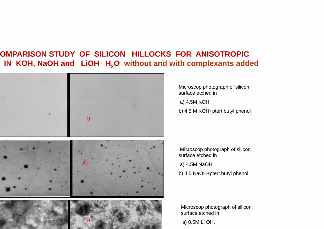
OMPARISON STUDY OF SILIC IN KOH, NaOH and LiOH ⋅ H
b
b
b
CON HILLOCKS FOR ANISOTROPIC H2O without and with complexants added
Microscop photograph of silicon surface etched in
a) 4 5M KOHa) 4.5M KOH,
b) 4.5 M KOH+ptert butyl phenol
Microscop photograph of silicon surface etched in
a) 4.5M NaOH,
b) 4.5 NaOH+ptert butyl phenol
Microscop photograph of silicon surface etched insurface etched in
a) 0.5M Li OH,

N OF BULK MICROMACH
micromachining technology is ailities in the field of sensors and m
Design of test structures for bucharacte
gn of test structures for characgy are important for:
minimizing the number of experim
optimisation and control of anisooptimisation and control of aniso
mask materials,
lithographic configuration,lithographic configuration,
establishing of design rules for 3
HINED SENSORSBulk micromachining technique
complex technique, offering a wide rangemicrosystems microfabrication.
ulk micromachining technology erisation
cterisation of 3D silicon micromachining
ments;
otropic etching processotropic etching process,
D microstructures,

DESIGN OF CONTROL ANDESIGN OF CONTROL AN
i th t t f t l dning the structures for control and
has a diamond cubic crystal sgraphic planes of silicon are <100
con etch rate in anisotropic solutie <110> direction and both are mu
different structures can be definedifferent structures can be defineask three different structures: onnd a square diaphragm on the b2.33 for silicon <110>)2.33 for silicon <110>)
hragm is defined by B++ doping.
> planes form (each one) an angleength of 54,740arctg√2
n <110> two of the planes <111>
D TEST STRUCTURES
Bulk micromachining technique
D TEST STRUCTURES
d t t it i t kd test it is necessary to know:
structure. The Miller indices of the main0>, <110>, and <111>
ions in the <100> direction is slightly higheruch higher than in the <111> direction
d in an unique process sequence by usingd in an unique process sequence, by usingne window which penetrates the wafer, a V-back side of the wafer (Fig.2.32, for silicon
e of 54,740 (for silicon <100>) and the slope
form an angle of 35 260 with the surface of

ing a diaphragm on silicon <
h2W ⋅+=
hing a V-groove on silicon <1
idth of the V-groove is √2 x thickidth of the V groove is √2 x thickched silicon
l = 2a = √ 2 x h
4,74° for Si <100>
Bulk micromachining technique
<100>
100>
kness ofkness of α

CMOS TECHNOLOGY AN
Bulk micromachining technique
D BULK MICROMACHINING

Sili fSilicon wafer
Deposit Positive Photoresist
Mask
UV Light
Develop resistp
Anneal and O id ti
Bulk micromachining technique
Oxidation
Open Contacts
DepositDeposit Aluminium
Pattern Aluminium
Pattern Back Oxide

PATTERNINGPATTERNINGk shown in Fig. 2.34. has only concif the opening is oriented properly
ORIENTAthe<110>
if the opening is oriented properlyed (Fig.2.35)
direction
G 1
Bulk micromachining technique
G -1cave corners, which are not usually y This way, the truncated pyramidal pit can
ATION in >
y. This way, the truncated pyramidal pit can
ns

PATTERNIN
FFaes
hip between opening surface orienhip between opening, surface orien
window Surface orientatio<100>
<100>
100
NG - 2Bulk micromachining technique
Fig.2.36. Undercuttting of improperlyFig.2.36. Undercuttting of improperly aligned edges. Improperly aligned edges are the corners on the right side
ntation and structurentation and structure
on StructurePyramidal pit or truncated pyramidal pity p py p
Rectangular pit (trench)
P id l i

PATTERNIN
nd experimentally that the undercnt of local surface area attacked bnt of local surface area attacked b
a, illustrates the pattern with two cna taking place during silicon etch
NG - 3Bulk micromachining technique
cutting depend on the total etching time and by the etchby the etch.
convex corners and the undercutting hing, Fig.2.37 b .

PATTERNIN
ral different examples of under
U d tti i i l t t
NG - 4Bulk micromachining technique
rcutting are shown in fig. 2.38-2.40
Fi 2 39 U d tti f d d

PATTERNIN
Fig.2.40. Undercutting progres
Bulk micromachining technique
NG - 5
ss in a cantilever array

PPLICATIONS ANDPIEZORESISTIVE PRESSUR
Bulk micromachining technique
EXAMPLESRE SENSOR

SiO2
Silicon
Si3N4
PhotoresistHardened resistMask
Silicon
SiO2
Si3N4
Silicon
SiO2Configured SiO2
Hardened resist
Silicon
Si N
SiO2
Piezoresistors
Bulk micromachining technique
Silicon
Si3N4
Piezoresistors
3 4
SiO
Silicon
SiO2
Piezoresistors
Si3N4Si3N4 – Plasma etched
Piezoresistors
Silicon –KOH etch
Si N Plasma
Silicon

of Science & technologyr R&D Programmeosystem Programmeosystem Programme
Bulk micromachining technique
Micro-capsule

tomotive Sensors
Vehicle Dynamic Control System
Crash Detection System
y y
Navigation Information SystemBody / Chassis Control System
Bulk micromachining technique
Satellite Sensor
Ai bAirbag
Seatbelt Sensor


Bulk micromachining technique

Bulk micromachining technique

SURFACE MICRO
Surface micromachining technique
OMACHINING

SURFACE MICROMACHIN
machining technology isof realisation of 3D micro
Isolation
of realisation of 3D micro-echanical structures from
s deposited and patternedfsurface.
Polysilicon
PSG
Oxide undoped 1
Oxide undoped 2Si3N4
p
Sacrificial layer NING TECHNOLOGY
S b t t
n
Substrate
sacrificiu
1
SubstratSubstrat
Strat de izolare Strat activ Strat activ
Isolation
SubstratSubstrat

layer
layer
Sacrificial layer
Surface micromachining technique
Sacrificial layer
Isolation layer
Silicon substrate
Sacrificial layer
Isolation layer
Silicon substrate
Isolation layer

matic representation of PSG
on
sbϑdif = DHF with DHFδ
sCbC −
Surface micromachining technique
sacrificial etching mechanism
1→External Reactant Mass Transport
2→Reactant diffusion2→Reactant diffusion
3→Product Diffusion
4→External product Mass transport
F = diffusion length

h l i l i t f th dhnological experiments for the deplayers – PSG – for surface microm
sition and etching of PSG thin filmssition and etching of PSG thin films
he PSG layers, generally considereding the APCVD method, typically atg , yp ysphine (2), in the presence of oxygen.
iH + 2O = SiO + 2H O4 2 2 2iH 2O SiO 2H OPH + 4O = P O + 3H O
4 2 2 2
3 2 2 5 2
hin SiO2 layers and PSG oxides, wihave been studied.
he etching speed has been analysedhe etching speed has been analysedones, using BHF-type etching so
th concentrations of 1:10 and 1:15 the
iti d fi ti f th
Surface micromachining technique
position and configuration of the machined membranes
d to be phosphor-doped silicon dioxide, are400oC and atmospheric pressure, from silanep p ,
ith phosphorus concentrations between 3 and
d for the densified oxides and also for thed, for the densified oxides, and also for theolutions (fluorhydric acid with ammoniumeir temperature being 35oC

BHF1:10d3 6,5 11,5 13
BHF1:10
%wt. P
speed for deposited layers, and for deposited and p p y , pin BHF 1:10
te of the doped CVD oxides (the Present a nonlinear increase vs. thensified oxides than for the densifiee the etching mechanism is differe
se in the etching rate swith the P c
Surface micromachining technique
80100120
140160
A/s
BHF1:15d020406080A
0 3 6,5 11,5 13
BHF1:15BHF1:15d
%wt. P
Fig.3.2. Etching speed for deposited layers, and for deposited and g g p p y , pdensified layers, in BHF 1:15
PSG ones) and the undoped ones, in BHF 1:10 e P concentration increase and they are higher ed ones, except for the very high P doped , p y g pent.
concentration is explained by the fact that the

. Etching of the sacrificial layer
e PSG etching under the resist andicon mask in BHF 15:1, vs. thehe SiO2 deposited layerhe SiO2 deposited layer
Surface micromachining technique
r
Fig.4.4. The PSG etching under the resist andthe polysilicon mask in BHF 15:1, vs. thedoping of the SiO deposited layerdoping of the SiO2 deposited layer

HE POLYSILICON LAYER DEP
D image of thesited” layers
and 53 Pa
Fig. 3.8-b. AFM 3-D imaLPCVD “as-deposited”surface, at 500oC andpressure.
e dimensions:nm.
Ra): 0.6393
The scanned surface dim1009.804 x 1005.637 nm.Medium rugosity (Ra): 1nm.
Fig 3 9-b AFig. 3.9-b. ALPCVD “surface, atpress re
Surface micromachining technique
POSITION
Fig. 3.9-a. AFM 3-D image of theage of the” layers
100 Pa
LPCVD “as-deposited” layerssurface, at 615oC and 20 Papressure.
The scanned surface dimensions:mensions:
.0387
1011.4 x 1012.1 nm.Medium rugosity (Ra): 20.2348 nm.
AFM 3-D image of theAFM 3-D image of the“as-deposited” layers
615oC and 100 Pa

sonant gas sensors susonant gas sensors su
The resonant gas sensorof a resonant polysiliconge and the measuremento pick up the resonanceof the bridge. By coatingwith sensor active material
ble to use these devices asitive gas sensor
urface micromachinedSurface micromachining technique
urface micromachined
P+ P+
Layout of a resonant sensor: microbridge withLayout of a resonant sensor: microbridge with excitation-detection electrodes

sonant gas sensors -2
a) Sensor chiptop view: a)b) electronic
electronic circuits for excitation -the microbridge, having the ma
ed by the variable capacitors from
the microresonator and the excie single-crystal silicon. The techg yd clamped polysilicon bridge withS technology.
Surface micromachining technique
The polysilicon microbridge is 1µm thickness. The polysilicon
pbridge; cs
1µm thickness. The polysilicon deposition for the bridge was realised by LPCVD, followed by lithographic configuration and planar plasma (CF4+O2) etching. The sacrificial oxide was then removed in BHF 10:1,
detection are integrated on the same chipain aim to amplify the small current (pA)
detection way.
itation-detection circuits are processed onhnological steps for processing a double-g g
electronics on the same chip are based on
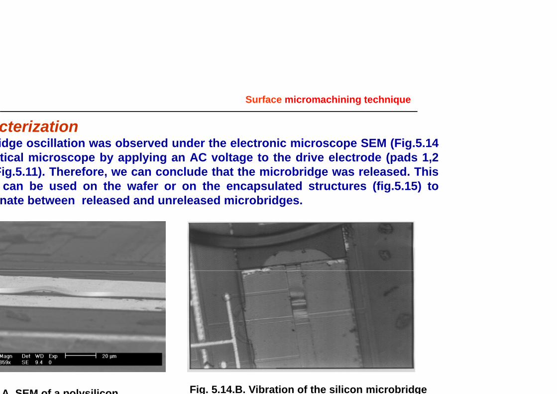
cterizationcterizationidge oscillation was observed undtical microscope by applying an
Fig.5.11). Therefore, we can conclug ) ,can be used on the wafer or onate between released and unrele
A SEM of a polysilicon
Surface micromachining technique
der the electronic microscope SEM (Fig.5.14AC voltage to the drive electrode (pads 1,2ude that the microbridge was released. Thisgn the encapsulated structures (fig.5.15) toeased microbridges.
Fig. 5.14.B. Vibration of the silicon microbridge

TEGRATED GAS MICROICATIONS IN ENVIRONM
ERISTICS :gases (NOx, CO, H2S) from media
nsions - chip area: 1 4x1 5 mm2nsions - chip area: 1,4x1,5 mm2,- electronic circuits
n the same chip with the sensorfactor: 1.000 in air, 20.000 in vacuum
measurement: ppm ÷ hundred ppmmeasurement: ppm ÷ hundred ppm,equency range: tens kHz÷MHz
OSENSOR WITH Surface micromachining technique
ENT MONITORINGSEM picture of a
polysilicon microbridge (400x30 µm2) in vibration(400x30 µm ) in vibration

CAPACITIVE PRESSUCAPACITIVE PRESSU
ve sensors convert a change ingd into a change of capacitancecapacitor consist basically of
rode separated by a dielectriccitance change can be used
motion of one of the twos with respect to the other
or by the change in theor by the change in thebetween two fixed electrodes.electrode movement is notr if the capacitance change isr if the capacitance change is
by deflection of part of thethen the capacitance changecalculated by integrating over
deformed dielectric space:
he two dimensional function w(x y) gives
URE MICROSENSORURE MICROSENSOR
Difragma din poliimida
ElectrodCr/Au/CrPoliimida
ElectrodCr/Au/CSiO2
ElectrodCr/Au/Cr
Si
ε
Cross section of the capacitive pressure microsensor
∫∫ −−=∆ dxdy
y)W(x,dεCC 0
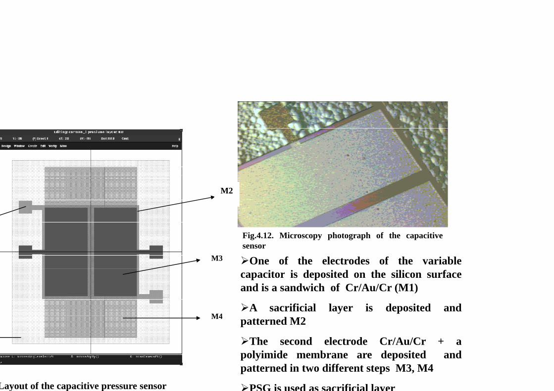
Layout of the capacitive pressure sensor
M2
Fig.4.12. Microscopy photograph of the capacitivesensor
M3 One of the electrodes of the variable
M4
capacitor is deposited on the silicon surfaceand is a sandwich of Cr/Au/Cr (M1)
A sacrificial layer is deposited andM4 patterned M2
The second electrode Cr/Au/Cr + apolyimide membrane are deposited andpatterned in two different steps M3, M4
PSG is used as sacrificial layer

acitive pressure sensoracitive pressure sensor
0.2 0.4 0.6 0.8 1 1.2 1.4 1.6 1.8
Rel. pressure (atm)
Relative capacitance change vs. applied differential pressure
Si3N4
SiliconA p<100>
Cr/Au
Bp<100>
Sacrificial layer
Cp<100>
C
Cr/Auu
D p<100>
Polyimide
E p<100>
PolyimideCr/AuCr/Au


NOSE – Operation princNOSE Operation princciplecipleEight cantilevers functionalized with i h diffeight different
polymers or blends


plications and examples
EMBRANE BASEMBRANE BASSED SENSORSSED SENSORS

MORESISTIVE GAS SENSORcation
Meron (9⋅1015 cm-2, 100lanted and diffused
b d i f
cation
CVD -SiO2
Lift ff
a boron doping from+ diffusion (1050°C, 4e p-n junction, 12 µmotropical stop etch
SiO25000
Lift-off mask
otropical stop etch
layer deposition andof the masking layer for
t hi f ili
Si N
5000 Å
etching of silicon
d configuration of aoped polysilicon layer.
Sin <10>
Si3N42000Å
sion could be to use thee high doped with boront polysilicon resistor-
is deposed such asr and the contacts at
RS - Sensor design and
Polysilicon 4000 Åetal
Electrodes
00B++

MORESISTIVE GAS SENSORriments -1
nterdigitated electrodes, the resisi th hi t t d toring the chip temperature and t
y bond pads are definedography above the insulated hea
(Cr-Au) was used as electrot hi d t t ith tto achieve a good contact with tThe utilisation of Al as electro
give us, also, very good results.
osition and the configurationside alignment of 2 µh ili t l (BPSG)sphosilicate glass (BPSG), as ma
for the anisotropic etching, wh
RS Phtalocyanine based –
storththeby
ater
odeth SEM picture of the sensor chiptheode
SEM picture of the sensor chip
byµm
kaskich

EMFET sensors
selectiveGas selective
E l tiEnzyme selectiveImmuno-selective
Fig. 1

FET BASED SENSORS FO
ct gas sensors are based on mmetal gate is a catalyst for gas s
FET BASED SENSORS FO
metal gate is a catalyst for gas sn are palladium, platinum, and irid
T Sensors use the field effectT Sensors use the field effectare biological and medical applic
m for a generating potential thay. The CHEMFET is essentially anthe transistor and the reference elec
OR MONITORING OF GASES
metal-insulator-semiconductor structures insensing Typical catalytic metals used in this
OR MONITORING OF GASES
sensing. Typical catalytic metals used in thisdium.
transistors to detect chemical quantities.transistors to detect chemical quantities.cations. The surface field effect is a desirableat provides high chemical selectivity and
n extended gate field effect transistor with thectrode

MANUFACT
Si3N4Polysilicon
p+ oxide
ate
CVD oxide
TiW/Au
Polysilicon
TURING STEPS
Separation
Si Substrate
b
EDP etching
d

MICROMACHINED
l micrograph of the body of the microping at the external package is presente
The body of the microprobe and the ads (optical microphotography) after 5h
etching in EDP, 96 0C
D MICROPROBE -1
probe which hosts the electronics and allows the ed in fig.4. and the microprobe tip is presented in
Fig.7.5. Optical microphotography (x100) of the microprobe tip, after 5h etching in EDP, 96 0C

BASED BIOSENSORS FOR MBASED BIOSENSORS FOR MIONS AND pH IN VITRO ANDIONS AND pH IN VITRO ANDIONS AND pH, IN VITRO ANDIONS AND pH, IN VITRO AND
e microprobe ISFET biosensors
ONITORING OF THE CaONITORING OF THE Ca+2+2, Mg, Mg+2+2, , D IN VIVOD IN VIVO 22D IN VIVO D IN VIVO --22
ISFET biosensor with integrated reference electrodeelectrode

OLYMER MICROMACHININGMicrofluidic channels

er Micromachined platform

ss micromachining
t etching (isotropic or anisotro
tal deposition+ lithography fortal deposition+ lithography for
sma treatment for resist remov
sma treatment for surface func
opic) of glass
r sensor patterningr sensor patterning
val
ctionalization

nsors platform

machining of ceramicsmachining of ceramics
veloping a novel class
aturized
rs
aturizedcost power consumption
g mixed techniques such as:
illi t h ir milling techniques;ductive ceramic technology;& thick film technology;micromachining techniquesmicromachining techniques
ss
s of chemoresistive gas

CAS 2005, 4th Octobe
DDesign and technologesign and technologhe sensor consists of an integrated on top of a suspended membrane.
P AP A.er machining of electroceramic heatennels (100 µm width) & subsequent fillinconducting ceramic
Heater(Mask
er, 30, 2005, Sinaia, Romania
gical stepsgical stepsheater and a platinum temperature sensor
STEP B. erng
SDeposition and configuration of an electric isolating layer (SiO2 or ceramic).
r 1)
Dielectric layer (Mask 2)

CAS 2005, 4th Octobe
DDesign and technesign and techn
Interdigitated ele
Heater
Insulator
strate
Fig.8. Mask
er, 30, 2005, Sinaia, Romania
ological stepsological steps
ectrodes SnO2 sensing material
6 - Membrane releasing

Manufacturining the heater groove
Manufacturining the heater groove
g the groove with AuPtPd paste
ning and release of the heater Thening and release of the heater. Theation was performed first by machbridges around the heater. This opcompleted by traversing the 0.5x2 ngles several times until the full thngles several times until the full the wafer was machined, resulting inngular hole.
hinning of the ceramic substrate bhinning of the ceramic substrate bwas performed by “scanning” the with the laser beam as shown in the the lateral step size (s) was 6 µm
ring Stepsring Steps
e releasinge releasing ining the
peration mm
hicknesshickness n a
back sideThe suspended heating element
back side. 3x3 mm
he Figure, m.

ent of the thermal properties
500,0°C
400
500
200
300
SP01
T
21,5°C
100
Turt
he heat distribution from the released ating element using FLIR 40
let
Twtcnh
400
500
C )
100
200
300
Tem
p (°C
The temperature is0
0 1 2 3 4 5
Time (s)
The temperature is uniform at the released area and he outside area at
The power-on curve for the released heater element.
east 400 °C lower emperature.
The input power p pwas 1,1 W and his should be
compared with the non-released heater element

eses
Ristic, Sensor Technology and Devices, A
. Seidel, L. Csepregi, A. Heuberger, H, p g , g ,n Alkaline Solutions, Journal of the Elec
Moldovan, R. Iosub, D. Dascalu, Gh. Nfor Silicon Anisotropic Etching, Abstfor Silicon Anisotropic Etching, AbstEtching of Silicon, Holten, 1998, pp 21
D. Gutsche, B. Dhawan, K. Hyum No,ization and Properties of the Calixarenization, and Properties of the Calixaren
1), 3782-3792
Shinkai, K. Araki, J. Shibata, D. Tsunga[4] S b tit t Eff t th Ux[4] arene: Substituent Effects on the U
in Trans.1 (1990), 3333-3337
inus Pauling, General Chemistry, W.in Bucharest 1972, pp. 461-462
K Sato M Shikida Y Matsushima T
Artech House, Boston, 1994, pp 67-68
H. Baumgärtel, Anisotropic Etching of Crystallineg , p g yctrochemical Society, 137 (1990), 3612-3632
Nechifor, C. Radu, An investigation of an Alkalinetract, Workshop of Physical Chemistry of Wettract, Workshop of Physical Chemistry of Wet-22
R. Mathukrishnan, Calixarenes. 4. The Synthesis,nes from p tert Butylphenol J Am Chem Socnes from p-tert- Butylphenol, J. Am. Chem Soc.,
awa, O. Manabe, Autoaccelerative Diazo CouplingU l C ti it f th OH G J ChUnusual Co-operativity of the OH Groups, J. Chem.
.H. Freeman and Company, San Francisco, 1970,
Yamashiro K Asaumi Y Iriye M Tamamoto

n, M. L. Reed, H. Han and R. Boudreauectromechanical Systems, 5 (1996), 65-
. M. M. C. Bressers, J. J. Kelly, J. Ggy of p-Type (100) Silicon Etched igy p yp ( )emical Society, 143 (1996), 1744-1750
Elwenspoek, Stationary Hillocks ohanics Europe Workshop MME'98, Ulvhanics Europe Workshop MME 98, Ulv
Schröder, E. Obermeier, A. Steckenmids on KOH etched {100} silicon Pmids on KOH etched {100} silicon, PMME'98, Ulvik in Hardanger, Norway,
Abe, A Contamination-Free Microstrucf H d hili d H d h bion of Hydrophilic and Hydrophobic
7 (1998), 94-101
, Mechanism of Etch Hillock Formation, Journal71
G. E. Gardeniers and M. Elwenspoek, Surfacein Aqueous Alkaline Solution, Journal of theq
on Etching Silicon, Proceedings, The Ninthvik in Hardanger, Norway,June 3-5, 1991, pp 70-vik in Hardanger, Norway,June 3 5, 1991, pp 70
nborn, Formation, prevention and removal ofProceedings The Ninth Micromechanics EuropeProceedings, The Ninth Micromechanics Europe
June 3-5, 1991, pp 28-31
ture in a Humid Environment by Means of aS f J l f Mi l t h i lc Surfaces, Journal of Microelectromechanical