Microfluidic metamaterial sensor: Selective trapping … · The meta-material was designed by...
7
Microfluidic metamaterial sensor: Selective trapping and remote sensing of microparticles Kailing Shih, Prakash Pitchappa, Manukumara Manjappa, Chong Pei Ho, Ranjan Singh, and Chengkuo Lee Citation: J. Appl. Phys. 121, 023102 (2017); doi: 10.1063/1.4973492 View online: http://dx.doi.org/10.1063/1.4973492 View Table of Contents: http://aip.scitation.org/toc/jap/121/2 Published by the American Institute of Physics
Transcript of Microfluidic metamaterial sensor: Selective trapping … · The meta-material was designed by...

Microfluidic metamaterial sensor: Selective trapping and remote sensing ofmicroparticlesKailing Shih, Prakash Pitchappa, Manukumara Manjappa, Chong Pei Ho, Ranjan Singh, and Chengkuo Lee
Citation: J. Appl. Phys. 121, 023102 (2017); doi: 10.1063/1.4973492View online: http://dx.doi.org/10.1063/1.4973492View Table of Contents: http://aip.scitation.org/toc/jap/121/2Published by the American Institute of Physics

Microfluidic metamaterial sensor: Selective trapping and remote sensing ofmicroparticles
Kailing Shih,1,2,5 Prakash Pitchappa,1,2 Manukumara Manjappa,3,4 Chong Pei Ho,1,2,5
Ranjan Singh,3,4 and Chengkuo Lee1,2,6,a)
1Department of Electrical and Computer Engineering, National University of Singapore, 117576 Singapore2Center for Intelligent Sensors and MEMS (CISM), National University of Singapore, 117576 Singapore3Division of Physics and Applied Physics, School of Physical and Mathematical Sciences,Nanyang Technological University, 637371 Singapore4Center for Disruptive Photonic Technologies, The Photonics Institute, 50 Nanyang Avenue,Nanyang Technological University, 639798 Singapore5Department of Micro/Nano Electronics, Shanghai Jiao Tong University, Dong Chuan Road 800,200240 Shanghai, People’s Republic of China6Graduate School for Integrative Science and Engineering, National University of Singapore, Singapore
(Received 2 November 2016; accepted 19 December 2016; published online 9 January 2017)
We experimentally demonstrate the integration of a microfluidic trap array on top of metamaterial
resonators for size selective trapping and remote sensing of microparticles. A split-ring resonator
(SRR) design supports strongly confined electric field in the capacitive split gap at the fundamental
inductive-capacitive resonance mode. The tightly confined electric field in the SRR gap forms a
hot-spot that has become an enabling platform for sensing applications. Here, we extend the con-
cept of metamaterial sensing to “trapping and sensing” by fabricating trapezoidal shaped structures
near the split gap that enables trapping of microparticles in the split-gap region of each SRR. The
proposed microfluidic metamaterial sensor enables sensing of different refractive index micropar-
ticles in terms of change in the transmitted amplitude and resonance frequency of the fundamental
resonance mode operating in the terahertz spectral region. The proposed approach exploits the
advantages offered by microfluidics, metamaterials, and terahertz technologies to form an ideal
platform for ultra-sensitive, label-free, remote, and non-destructive detection of micro-substances.
Published by AIP Publishing. [http://dx.doi.org/10.1063/1.4973492]
I. INTRODUCTION
An electromagnetic metamaterial is a periodic array of
sub-wavelength structures that can be engineered to achieve
specific electromagnetic properties on demand.1,2 This has led
to the demonstration of numerous interesting electromagnetic
properties such as negative refractive index,3,4 perfect absorp-
tion,5,6 sub-wavelength focusing,7 and many more.8–10
Interestingly, the properties of the metamaterials are strongly
dependent on the geometry of their unit cell, and thereby pas-
sively and actively varying the size and shape of the unit cell,
a precise control of the metamaterial properties can be readily
achieved.11–18 Alternatively, metamaterials are also explored
as a sensing platform due to their strong response to the
changes in the surrounding medium and strong enhancement
of the field strengths at specific portions of the resonator geom-
etry.19 In particular, metamaterials operating in the THz spec-
tral region are of great interest, due to their lower illumination
energy and their unit cell dimensions matching the size of
microscale particles and biological cells.20–24
Earlier reports have shown the sensing capabilities of
the THz metamaterials by covering the entire surface of the
metamaterial resonators with the material of interest for
sensing.25–33 Park et al., have reported detection of microor-
ganisms,25–27 while on the other hand chemical and biomole-
cule sensing has also been explored.28–33 However, these
reports provide the qualitative estimations on the sensing of
the thin film or biological samples in the form of their statis-
tical average value. These techniques also require a rela-
tively large volume of sensing medium due to the need for
uniform coating.34 Hence, to achieve more quantitative sens-
ing of particles, the number of particles per resonator geome-
try and the location at which the particle is placed become
extremely crucial. This can be realized by integrating micro-
fluidic trapping structures onto metamaterial resonators oper-
ating in the THz spectral range. Integration of metamaterials
and microfluidics has been demonstrated in the gigahertz
(GHz) spectral range for liquid sensing.35,36 Microfluidics
enables the precise manipulation of fluid with a small vol-
ume inside a microchannel by utilizing the microelectrome-
chanical system (MEMS) technology.37–41 It also facilitates
precise handling, sorting, and trapping of microsubstances
suspended in liquid solution.42–44 By proper design of the
flow resistance, a single particle trapping can be positioned
at the desired area of the microfluidic device.45–48 Hence, by
integrating microfluidic systems with metamaterials, it is
possible to control the volume of the sample and the location
of microsubstances without any chemical modification or
additional handling. Moreover, the versatility of metamate-
rial resonator designs with the ease of microfluidic integra-
tion offers a new set of interesting functionalities for
applications in the field of chemical and biological sensing.
In this work, we experimentally demonstrate a device
platform for trapping and sensing of microparticles by
a)Author to whom correspondence should be addressed. Electronic mail:
0021-8979/2017/121(2)/023102/6/$30.00 Published by AIP Publishing.121, 023102-1
JOURNAL OF APPLIED PHYSICS 121, 023102 (2017)
exploiting the advantages provided by the microfluidics and
metamaterials operating in the THz spectral region. The
device consists of microfluidic channels integrated with trap-
ping structures on top of a metamaterial structure to trap the
microparticles in the most sensitive region of each unit cell,
and the changes in the THz transmission response of the
metamaterial are used to examine the type and quantity of
the trapped microparticles.
II. DESIGN AND FABRICATION
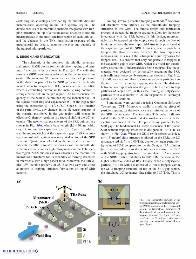
The schematic of the proposed microfluidic metamate-
rial sensor (MMS) device for the selective trapping and sens-
ing of microparticles is shown in Fig. 1(a). The split ring
resonator (SRR) structure is selected as the metamaterial res-
onator. The incoming THz wave with electric field polarized
in the direction parallel to the SRR gap excites the funda-
mental inductive-capacitive (LC) resonance of the SRR,
where a circulating current in the metallic ring confines a
strong electric field in the gap region. The LC resonance fre-
quency of the SRR is determined by the inductance (L) of
the square metal ring and capacitance (C) of the gap region
using the expression, fr ¼ 1=2pffiffiffiffiffiffi
LCp
. Since C is a function
of the permittivity, any changes in the dielectric property of
the material positioned in the gap region will change its
effective C, thereby resulting in a spectral shift of the LC res-
onance. The geometrical parameters of the SRR unit cell are
shown in Fig. 1(b), where base length (L)¼ 30 lm, width
(w)¼ 5 lm, and the capacitive gap (g)¼ 5 lm. In order to
trap the microparticles at the capacitive gap of SRR geome-
try, a microfluidic system was integrated on top of the SRR
structure. Quartz was selected as the substrate material to
fabricate metallic resonator patterns as well as microfluidic
structures because of its high transparency in the THz spec-
tral region. SU-8 photoresist was chosen as the material for
microfluidic structures for its capability of forming structures
in microscale with a high aspect ratio. Moreover, the ultravi-
olet (UV) curable property of SU-8 allows easy and direct
alignment of trapping structure fabrication on top of SRR
patterns.
Among several presented trapping methods,46 trapezoi-
dal structures were utilized as the microfluidic trapping
structures in this work. The simple design and fabrication
process of trapezoidal trapping structures allow for the easier
integration with the SRR below. In this design, micropar-
ticles can be trapped into the empty slots through the flow of
liquid in between the two trapezoidal structures positioned at
the capacitive gap of the SRR. However, once a particle is
trapped, the flow resistance between the two trapezoids
increases and as a result the subsequent liquid bypasses the
trapped slot. This ensures that only one particle is trapped at
the capacitive gap of each SRR, which is critical for quanti-
tative estimation of microparticles being trapped. The meta-
material was designed by periodically arranging the SRR
unit cells in a honeycomb structure, as shown in Fig. 1(c).
This allows the liquid flow to carry subsequent particles into
the next row of the empty trapping structures. The distance
between two trapezoids was designed to be t¼ 5 lm to trap
particles of larger size, in this case, aiming at polystyrene
particles with a diameter of 20 lm suspended in isopropyl
alcohol (IPA) solution.
Simulations were carried out using Computer Software
Technology (CST) Microwave studio to study the effect of
particle trapping on the resonance transmission response of
the SRR metamaterial. The incoming THz pulse is illumi-
nated on the SRR metamaterial at normal incidence with the
electric component of the THz pulse being parallel to the
SRR gap. The fundamental LC mode resonance of the planar
SRR without trapping structures is designed at 1.04 THz, as
shown in Fig. 2(a). When the SU-8 (with refractive index,
n¼ 1.8) microfluidic structure is placed on the SRR, the LC
resonance red shifts to 1.00 THz, due to the larger permittiv-
ity value of SU-8 compared to the air. Next, as IPA solution
(n¼ 1.9) was added into the whole area covering the SRR
with SU-8 trapping structures, the simulated LC resonance
of the SRRs further red shifts to 0.85 THz, because of the
higher refractive index of IPA. Finally, when a polystyrene
particle (n¼ 1.6) with a diameter of 20 lm is trapped within
the SU-8 trapping structure on top of the SRR gap region,
the simulated LC resonance blue shifts to 0.87 THz. This is
FIG. 1. (a) Schematic drawing of the
proposed microfluidic metamaterial sen-
sor (MMS) operating in the THz spectral
region. (b) Geometrical parameters of
the metamaterial unit cell along with the
trapping structure (g¼ 5lm, t¼ 5lm,
w¼ 5lm, L¼ 30lm) and (c) the corre-
sponding metamaterial array design
(p¼ 50 lm).
023102-2 Shih et al. J. Appl. Phys. 121, 023102 (2017)

caused due to the lower refractive index of polystyrene with
respect to IPA solution. The electric field distribution at the
fundamental LC resonant frequency of the SRR was studied at
various trapping configurations of the MMS. When no particle
is trapped, there is a strong confinement of electric field in the
capacitive gap region, as shown in Fig. 2(b). However, when
the particle is trapped, the electric field in the gap region
strongly couples to the particle, as shown in Fig. 2(d). This
causes a spectral shift of the SRR LC mode resonance. Hence,
based on the changes in the THz transmission spectral shift of
LC resonance, the type of microparticle can be estimated.
Further simulations were carried out to determine the
best particle trapping position on the SRR geometry to
achieve the maximum sensitivity. By setting the center of
the SRR gap region as the coordinate origin, the polystyrene
particle along with its trapping structure was moved to dif-
ferent spatial positions along x- and y- directions on top of
the SRR (Fig. 3(a)). The amount of resonance shift (Dfr) was
calculated as the difference between the initial resonance fre-
quency of the SRR with trapping structures plus the IPA
solution without the particle (0.85 THz) and with the particle
trapped at various spatial positions. As shown in Fig. 3(b),
the particle placed in the center of the gap region (x¼ 0 lm,
y¼ 0 lm) results in the largest shift of LC resonance. The
value of Dfr decreases along the y-direction at any fixed x-
position. This is due to the existence of stronger electric field
strength at the SRR gap as shown in Fig. 2(b) and the
strength fades out as the particle is displaced along the y-
direction. In the case of particle being displaced along the
x-direction (for y¼ 0), there is no significant change in the
frequency shift Dfr of the resonance. This observed distinc-
tive variation in the values of the frequency shifts Dfr along
the x- or y-axis displacement of the particle is due to the
anisotropic distribution of the confined electric field in the
x- and y-directions. In other words, the electric field distribu-
tion along the x-direction is more uniform than its distribu-
tion along the y-direction in the SRR gap region.
The steps involved in the fabrication process for the
demonstration of the MMS concept are shown pictorially in
Fig. 4. The UV lithography process was first performed to
structure the SRR patterns. Later, titanium (Ti) and alumi-
num (Al) metal of thickness 10 nm and 100 nm, respectively,
were deposited using a thermal evaporation method followed
by the lift-off process to obtain the desired metamaterial pat-
terns (Fig. 4(a.1)). The trapping structure and the microflui-
dic channel of 25 lm height were aligned and patterned on
top of each SRR gap using SU-8 photoresist (Fig. 4(a.2)). As
a sealing material, a polyethylene terephthalate (PET) sub-
strate of thickness 100 lm was used because of its high
FIG. 2. (a) Simulated THz transmission spectrum for the SRR under the fol-
lowing conditions of only SRR, SRR with the trapping structure, SRR with
the trapping structure plus IPA introduction, and SRR with the trapping
structure plus IPA plus the polystyrene particle. (b) Top view and (c) per-
spective view of the simulated electric field distribution of the SRR in IPA
at 0.85 THz when the particle is not trapped. (d) Top view and (e) perspec-
tive view of the simulated electric field distribution of SRR in IPA at 0.87
THz when the particle is trapped.
FIG. 3. (a) Schematic illustration of
displacing the particle with the trap-
ping structure from the center of
SRR’s gap. (b) Contour plot showing
the resonant frequency shift when the
particle is trapped at different positions
(along x and y axes) with respect to the
SRR gap (the black line indicates the
edge of the SRR structure).
023102-3 Shih et al. J. Appl. Phys. 121, 023102 (2017)
transparency in the THz and visible spectrum (Fig. 4(b.1)). It
was treated by oxygen (O2) plasma before spin-coating a
50 lm thick SU-8 as an adhesive layer (Fig. 4(b.2)).
Subsequently, the PET with uncrosslinked SU-8 was flipped
and bonded on top of the bottom SRR substrate with a SU-
8 trapping structure chip (Fig. 4(c)). Finally, the bonded
microfluidic chip was exposed to UV light to crosslink the
adhesive SU-8 layer, thereby making a strong seal to prevent
solution leakage during the measurements (Fig. 4(d)). Fig.
5(a) shows the photograph of the MMS device (1 cm� 1 cm)
fabricated on a quartz substrate of dimension 4 cm� 4 cm.
Fig. 5(b) depicts the microscopic image of the MMS active
area, where the trapping structures positioned on top of each
SRR with two trapezoidal structures are seen. Due to the lim-
itations of the alignment system for the photolithography
process, there is a slight misalignment of the trapping struc-
ture from the center of the SRR gap. In our fabrication, we
observed Dx¼þ4 lm and Dy¼þ5 lm alignment error,
respectively, along the horizontal and the vertical directions.
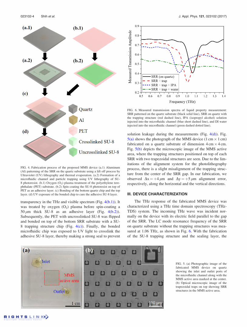
III. DEVICE CHARACTERIZATION
The THz response of the fabricated MMS device was
characterized using a THz time domain spectroscopy (THz-
TDS) system. The incoming THz wave was incident nor-
mally on the device with its electric field parallel to the gap
of the SRR. The LC mode resonance frequency of the SRR
on quartz substrate without the trapping structures was mea-
sured at 1.06 THz, as shown in Fig. 6. With the fabrication
of the SU-8 trapping structure and the sealing layer, the
FIG. 4. Fabrication process of the proposed MMS device (a.1) Aluminum
(Al) patterning of the SRR on the quartz substrate using a lift off process by
Ultraviolet (UV) lithography and thermal evaporation. (a.2) Formation of a
microfluidic channel and particle trapping using UV lithography of SU-
8 photoresist. (b.1) Oxygen (O2) plasma treatment of the polyethylene tere-
phthalate (PET) substrate. (b.2) Spin coating the SU-8 photoresist on top of
PET as an adhesive layer. (c) Bonding of the bottom quartz chip and the top
layer. (d) UV exposure of the bonded chip to cure the adhesive SU-8 layer.
FIG. 5. (a) Photographic image of the
fabricated MMS device on quartz
showing the inlet and outlet ports of
the microfluidic channel along with the
MMS active area marked at the center.
(b) Optical microscopic image of the
trapezoidal traps on top showing SRR
structures in the MMS active area.
FIG. 6. Measured transmission spectra of liquid property measurement:
SRR patterned on the quartz substrate (black solid line), SRR on quartz with
the trapping structure (red dashed line), IPA (isopropyl alcohol) solution
injected into the microfluidic channel (blue short dashed line), and DI water
injected into the microfluidic channel (green dashed dotted line).
023102-4 Shih et al. J. Appl. Phys. 121, 023102 (2017)

measured LC resonance frequency red shifts to 1.00 THz,
and shows good agreement with the simulated results. IPA
and deionized (DI) water were injected into the fluidics chan-
nel without any microparticles. When DI water was injected
into the channel, the amplitude of the transmitted THz signal
was strongly modulated and there was no observable reso-
nance dip in the measured spectrum. This is due to strong
absorption of water in the THz frequencies. Alternatively,
for IPA, the resonance is observed at 0.91 THz. The red shift
in the measured resonance frequency is caused due to the
increased refractive index of IPA relative to air. The integra-
tion of microfluidics channel structures and the metamaterial
enables detection of refractive index of liquids using a small
sample volume.
As a demonstration of particle trapping and detection,
polystyrene beads (Phosphorex) with a diameter of 20 lm
were used. After filling the channel with pure IPA, polysty-
rene beads suspended in IPA solution were injected using a
syringe pump. From optical microscopic observation, 15%
of the SRRs were occupied by beads in a random order. The
transmission spectrum of the trapped beads in IPA solution
was then measured and a resonance dip was observed at 0.92
THz, as shown in Fig. 7. The measured resonance frequency
shift of 10 GHz was achieved for the MMS with and without
polystyrene particles. The blue shift in the resonance is
caused due to the lower refractive index of polystyrene with
respect to IPA. The relatively small resonant shift in the
measurements can be attributed to the alignment errors in the
fabrication process and reduced number of particles trapped
in the SRR gaps. Since the transmitted signal is a collective
response of each meta-atom, the reduction in the number of
SRRs with trapped particles also results in a decrease of
resonance strength. Limitations such as the trapping rate
and alignment error can be readily overcome by further opti-
mization of resonator design, trapping structural design,
robust fabrication process, and experimental conditions.
Furthermore, the proposed MMS is an ideal platform for the
live biological cell trapping and detection; however the limi-
tation of water absorption should be addressed. This can be
done by reducing the water volume in the trapping struc-
tures. Thus, the proposed MMS device concept allows for
the label-free, non-destructive, and remote sensing of micro-
particles by taking advantage of the complementing features
offered by the research fields of microfluidics, metamateri-
als, and terahertz spectroscopy.
IV. CONCLUSION
In summary, a platform for size selective trapping and
sensing of microparticles is demonstrated by integrating
microfluidics with metamaterials operating at terahertz fre-
quencies. We designed and fabricated periodically spaced
SRR structures on a quartz substrate consisting of SU-8/PET
microfluidic channels to selectively trap the microparticles in
the most sensitive gap region of the SRRs. Due to the prede-
fined number of microparticles trapped in each SRR, the
THz transmission response can provide both the qualitative
and quantitative estimation of the trapped particles in terms
of their resonance frequency and the amplitude modulation,
respectively. The maximum blue shift of 10 GHz is achieved
for 15% particle trapping rate. The versatility of metamate-
rial resonator designs along with the selective trapping func-
tionality of microfluidics operating in the low energy THz
spectral range will open up new research opportunities
focused on label-free detection, biomolecular sensing and
quantification of microparticles in the terahertz and infrared
frequencies.
ACKNOWLEDGMENTS
K.S., P.P., C.P.H., and C.L. acknowledge the financial
support from the research grant of ARF Tier2-MOE2012-
T2-2-154; NRF-CRP15-2015-02 at the National University
of Singapore, Singapore. National Natural Science
Foundation of China under Grant No. 61474078 at NUS
(Suzhou) Research Institute, Suzhou, China, and No.
61674104 at Shanghai Jiao Tong University, Shanghai,
China. M.M. and R.S. acknowledge the research funding
support from NTU startup Grant No. M4081282, Singapore
MOE Grant Nos. M4011362, M4011534, MOE2011-T3-1-
005, and MOE2015-T2-2-103.
1B. Ferguson and X.-C. Zhang, “Materials for terahertz science and tech-
nology,” Nat. Mater. 1, 26 (2002).2N. I. Zheludev and Y. S. Kivshar, “From metamaterials to metadevices,”
Nat. Mater. 11, 917 (2012).3R. A. Shelby, D. R. Smith, and S. Schultz, “Experimental verification of a
negative index of refraction,” Science 292, 77 (2001).4J. Valentine, S. Zhang, T. Zentgraf, E. Ulin-Avila, D. A. Genov, G. Bartal,
and X. Zhang, “Three-dimensional optical metamaterial with negative
refractive index,” Nature 455, 376 (2008).5H. Tao, N. I. Landy, C. M. Bingham, Z. Zhang, R. D. Averitt, and W. J.
Padilla, “A metamaterial absorber for the terahertz regime: Design, fabri-
cation and characterization,” Opt. Express 16, 7181 (2008).6N. I. Landy, S. Sajuyigbe, J. J. Mock, D. R. Smith, and W. J. Padilla,
“Perfect metamaterial absorber,” Phys. Rev. Lett. 100, 207402 (2008).7N. Fang, H. Lee, C. Sun, and X. Zhang, “Sub-diffraction-limited optical
imaging with a silver superlens,” Science 308, 534 (2005).
FIG. 7. Measured transmission spectra of the bead trapping experiment:
SRR with trap (black solid line), SRR with trap in IPA solution (red solid
line), and polystyrene beads trapped in IPA solution (red dashed line), and
the inset figure depicts the optical microscopic image of polystyrene beads
trapped by the SU-8 trapping structure at the gap of the SRR pattern.
023102-5 Shih et al. J. Appl. Phys. 121, 023102 (2017)

8P. Pitchappa, M. Manjappa, C. P. Ho, R. Singh, N. Singh, and C. Lee,
“Active control of electromagnetically induced transparency analog in ter-
ahertz MEMS metamaterial,” Adv. Opt. Mater. 4, 541 (2016).9C. P. Ho, P. Pitchappa, and C. Lee, “Digitally reconfigurable binary coded
terahertz metamaterial with output analogous to NOR and AND,” J. Appl.
Phys. 119, 153104 (2016).10D. Hasan, C. P. Ho, and C. Lee, “Thermally tunable absorption-induced
transparency by a quasi 3D bow-tie nanostructure for nonplasmonic and
volumetric refractive index sensing at mid-IR,” Adv. Opt. Mater. 4, 943
(2016).11D. Schurig, J. J. Mock, B. J. Justice, S. A. Cummer, J. B. Pendry, A. F.
Starr, and D. R. Smith, “Metamaterial electromagnetic cloak at microwave
frequencies,” Science 314, 977 (2006).12F. Ma, Y.-S. Lin, X. Zhang, and C. Lee, “Tunable multiband terahertz
metamaterials using a reconfigurable electric split-ring resonator array,”
Light: Sci. Appl. 3, e171 (2014).13P. Pitchappa, C. P. Ho, L. Dhakar, Y. Qian, N. Singh, and C. Lee,
“Periodic array of subwavelength MEMS cantilevers for dynamic
manipulation of terahertz waves,” J. Microelectromech. Syst. 24, 525
(2015).14P. Pitchappa, C. P. Ho, Y. Qian, L. Dhakar, N. Singh, and C. Lee,
“Microelectromechanically tunable multiband metamaterial with pre-
served isotropy,” Sci. Rep. 5, 11678 (2015).15P. Pitchappa, C. P. Ho, L. Dhakar, Y. Qian, and C. Lee,
“Microelectromechanically reconfigurable interpixelated metamaterial for
independent tuning of multiple resonances at terahertz spectral region,”
Optica 2, 571 (2015).16Y.-S. Lin and C. Lee, “Tuning characteristics of mirrorlike T-shape tera-
hertz metamaterial using out-of-plane actuated cantilevers,” Appl. Phys.
Lett. 104, 251914 (2014).17P. Pitchappa, C. P. Ho, L. Cong, R. Singh, N. Singh, and C. Lee,
“Reconfigurable digital metamaterial for dynamic switching of terahertz
anisotropy,” Adv. Opt. Mater. 4, 391 (2016).18P. Pitchappa, M. Manjappa, C. P. Ho, R. Singh, N. Singh, and C. Lee,
“Active control of electromagnetically induced transparency with dual
dark mode exciatation pathway using MEMS based tri-atomic meta-
molecules,” Appl. Phys. Lett. 109, 211103 (2016).19T. Chen, S. Li, and H. Sun, “Metamaterials application in sensing,”
Sensors 12, 2742 (2012).20M. Tonouchi, “Cutting-edge terahertz technology,” Nat. Photonics 1, 97
(2007).21R. M. Woodward, B. E. Cole, V. P. Wallace, R. J. Pye, D. D. Arnone, E.
H. Linfield, and M. Pepper, “Terahertz pulse imaging in reflection geome-
try of human skin cancer and skin tissue,” Phys. Med. Biol. 47, 3853
(2002).22H. B. Liu, G. Plopper, Y. Chen, B. Ferguson, and Z.-C. Zhang, “Sensing
minute changes in biological cell monolayers with THz differential time-
domain spectroscopy,” Biosens. Bioelectron. 22, 1075 (2007).23A. Menikh, R. MacColl, C. A. Mannella, and X.-C. Zhang, “Theahertz
biosensing technology: Frontiers and progress,” ChemPhysChem 3, 655
(2002).24C. Seco-Martorell, V. Lopez-Dominguez, G. Arauz-Garofalo, A. Redo-
Sanchez, J. Palacios, and J. Tejada, “Goya’s artwork imaging with
Terahertz waves,” Opt. Express 21, 17800 (2013).25S. J. Park, J. T. Hong, S. J. Choi, H. S. Kim, W. K. Park, S. T. Han, J. Y.
Park, S. Lee, D. S. Kim, and Y. H. Ahn, “Detection of microorganisms
using terahertz metamaterials,” Sci. Rep. 4, 4988 (2014).26S. J. Park, B. H. Son, S. J. Choi, H. S. Kim, and Y. H. Ahn, “Sensitive
detection of yeast using terahertz slot antennas,” Opt. Express 22, 30467
(2014).27S. J. Park, S. W. Jun, A. R. Kim, and Y. H. Ahn, “Terahertz metamaterial
sensing on polystyrene microbeads: Shape dependence,” Opt. Mater.
Express 5, 2150 (2015).
28J. F. O’Hara, R. Singh, I. Brener, E. Smirnova, J. Han, A. J. Taylor, and
W. Zhang, “Thin-film sensing with planar terahertz metamaterials:
Sensitivity and limitations,” Opt. Express 16, 1786 (2008).29R. Singh, W. Cao, I. Al-Naib, L. Cong, W. Withayachumnankul, and W.
Zhang, “Ultrasensitive terahertz sensing with high-Q Fano resonances in
metasurfaces,” Appl. Phys. Lett. 105, 171101 (2014).30L. Cong, S. Tan, R. Yahiaoui, F. Yan, W. Zhang, and R. Singh,
“Experimental demonstration of ultrasensitive sensing with terathertz
metamaterial absorbers: A comparison with the metasurfaces,” Appl.
Phys. Lett. 106, 031107 (2015).31D.-K. Lee, J.-H. Kang, J.-S. Lee, H.-S. Kim, C. Kim, J. H. Kim, T.
Lee, J.-H. Son, Q-H. Park, and M. Seo, “Highly sensitive and selec-
tive sugar detection by terahertz nano-antennas,” Sci. Rep. 5, 15459
(2015).32O. Limaj, D. Etezadi, N. J. Wittenberg, D. Rodrigo, D. Yoo, S.-H. Oh, and
H. Altug, “Infrared plasmonic biosensor for real-time and label-free moni-
toring of lipid membranes,” Nano Lett. 16, 1502 (2016).33A. Berrier, M. C. Schaafsma, G. Nonglaton, J. Bergquist, and J. G. Rivas,
“Selective detection of bacterial layers with terahertz plasmonic antennas,”
Biomed. Opt. Express 3, 2937 (2012).34W. Withayachumnankul, H. Lin, K. Serita, C. M. Shah, S. Sriram, M.
Bhaskaran, M. Tonouchi, C. Fumeaux, and D. Abbott, “Sub-diffraction
thin-film sensing with planar terahertz metamaterials,” Opt. Express 20,
3345 (2012).35W. Withayachumnankul, K. Jaruwongrungsee, A. Tuantranont, C.
Fumeaux, and D. Abbott, “Metamaterial-based microfluidic sensor for
dielectric characterization,” Sens. Actuators, A 189, 233 (2013).36A. Ebrahimi, W. Withayachumnankul, S. Al-Sarawi, and D. Abbott,
“High-sensitivity metamaterial-inspired sensor for microfluidic dielectric
characterization,” IEEE Sens. J. 14, 1345 (2014).37G. M. Whitesides, “The origins and the future of microfluidics,” Nature
442, 368 (2006).38L. Y. Yeo, H.-C. Chang, P. P. Y. Chan, and J. R. Friend, “Microfluidic
devices for bioapplications,” Small 7, 12 (2011).39J. El-Ali, P. K. Sorger, and K. F. Jensen, “Cells on chip,” Nature 442, 403
(2006).40R. Sista, Z. Hua, P. Thwar, A. Sudarsan, V. Srinivasan, A. Eckhardt, M.
Pollack, and V. Pamula, “Development of a digital microfluidic platform
for point of care testing,” Lab Chip 8, 2091 (2008).41H. Wang, C.-H. Chen, Z. Xiang, M. Wang, and C. Lee, “Convection-
driven long-range linear gradient generator with dynamic controls,” Lab
Chip 15, 1445 (2015).42X. Fan, I. M. White, S. I. Shopova, H. Zhu, J. D. Suter, and Y. Sun,
“Sensitive optical biosensors for unlabeled targets: A review,” Anal.
Chem. Acta 620, 8 (2008).43K. K. Zeming, S. Ranjan, and Y. Zhang, “Rotational separation of non-
spherical bioparticles using I-shaped pillar arrays in a microfluidic
device,” Nat. Commun. 4, 1625 (2013).44M. E. Warkiani, G. Guan, K. B. Luan, W. C. Lee, A. A. S. Bhagat, P. K.
Chaudhuri, D. S.-W. Tan, W. T. Lim, S. C. Lee, P. C. Y. Chen, C. T. Lim,
and J. Han, “Slanted spiral microfluidics for the ultar-fast, label-free isola-
tion of circulating tumor cells,” Lab Chip 14, 128 (2014).45D. Di Carlo, L. Y. Wu, and L. P. Lee, “Dynamic single cell culture array,”
Lab Chip 6, 1445 (2006).46X. Xhu, P. Sarder, Z. Li, and A. Nehorai, “Optimization of microfluidic
microsphere-trap arrays,” Biomicrofluidics 7, 014112 (2013).47J. Kim, J. Erath, A. Rodriguez, and C. Yang, “A high-efficiency microflui-
dic device for size-selective trapping and sorting,” Lab Chip 14, 2480
(2014).48H. Chen, J. Sun, E. Wolvetang, and J. Cooper-White, “High-throughput,
deterministic single cell trapping and long-term clonal cell culture in
microfluidic devices,” Lab Chip 15, 1072 (2015).
023102-6 Shih et al. J. Appl. Phys. 121, 023102 (2017)