Microfabrication - ERNETsuresh/memscourse/proflectures/lecture3.pdfMicrofabrication Process Flows...
59
Microfabrication Process Flows G. K. Ananthasuresh [email protected] Mechanical Engineering Indian Institute of Science Bangalore, INDIA February 19 th , 2005 http://www.mecheng.iisc.ernet.in/~suresh/memscourse/proficience33.html Presented to Proficience #33 class in Jan.-May term of 2005 Lecture 3
Transcript of Microfabrication - ERNETsuresh/memscourse/proflectures/lecture3.pdfMicrofabrication Process Flows...

MicrofabricationProcess Flows
G. K. [email protected] EngineeringIndian Institute of ScienceBangalore, INDIA
February 19th, 2005http://www.mecheng.iisc.ernet.in/~suresh/memscourse/proficience33.html
Presented to Proficience #33 class in Jan.-May term of 2005
Lecture 3

G.K. Ananthasuresh, Indian Institute of Science, Jan. 2005
2Equipment and Process Flows
Basic equipment
Pressure sensor process steps
Process steps for comb-drive
Process steps for in-plane hinges
MUMPs (foundry process)
Resonant pressure sensor
PennSOIL
Electronics integration and packaging

G.K. Ananthasuresh, Indian Institute of Science, Jan. 2005
3Basic process steps
PhotolithographyOxidationThin-film depositionSelective etching through a maskWafer bondingDopingEpitaxial growthThick-film depositionDicing, die-bonding, and wire-bonding

G.K. Ananthasuresh, Indian Institute of Science, Jan. 2005
4Silicon wafer making
(from “Fundamental of Microfabrication” by Marc Madou)

G.K. Ananthasuresh, Indian Institute of Science, Jan. 2005
5Oxidation
(from “Fundamental of Microfabrication” by Marc Madou)

G.K. Ananthasuresh, Indian Institute of Science, Jan. 2005
6Physical vapour deposition (PVD)
(from “Fundamental of Microfabrication” by Marc Madou)

G.K. Ananthasuresh, Indian Institute of Science, Jan. 2005
7Chemical vapour deposition (CVD)
(from “Fundamental of Microfabrication” by Marc Madou)

G.K. Ananthasuresh, Indian Institute of Science, Jan. 2005
8PECVD (plasma-enhanced)
(from “Fundamental of Microfabrication” by Marc Madou)

G.K. Ananthasuresh, Indian Institute of Science, Jan. 2005
9Process design issues
Geometry of the deviceAvailable equipment and skillsSystem partitioningProcess partitioningContamination and cleaning requirmentsMaterial property controlProcess accuracyMechanical and thermal stabilityAlignment featuresPlanning the devices on the waferPost-fabrication (packaging)

G.K. Ananthasuresh, Indian Institute of Science, Jan. 2005
10A typical process flow
Begin with substrate waferRCA clean with HF dipGrow oxidePhotolithography (alignment)Etch alignment marks into oxideStrip photoresistPhotolithography (piezoresistors)Boron implantingStrip photoresistRCA clean without HF dipDeposit nitrideBackside photolithography (diaphragm)Etch nitride and oxide from backKOH etchPhotolithography (vias)Plasma etch nitride and oxide through viasStrip photoresistPre-metal cleanEvoporate aluminiumPhotolithography (aluminum)Strip photoresistSinter for annealing contactsTest piezoresistor value at the wafer levelDie separation with sawingMount in packageWire-bondSeal packageTest and calibration
For Motorola’s pressure sensor

G.K. Ananthasuresh, Indian Institute of Science, Jan. 2005
11MIT’s wafer-bonded pressure sensor
G.K. Ananthasuresh, Indian Institute of Science, Jan. 2005
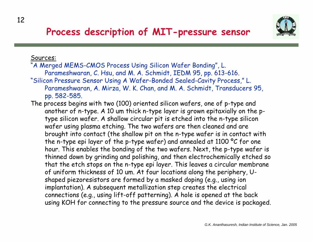
12Process description of MIT-pressure sensor
Sources:“A Merged MEMS-CMOS Process Using Silicon Wafer Bonding”, L.
Parameshwaran, C. Hsu, and M. A. Schmidt, IEDM 95, pp. 613-616.“Silicon Pressure Sensor Using A Wafer-Bonded Sealed-Cavity Process,” L.
Parameshwaran, A. Mirza, W. K. Chan, and M. A. Schmidt, Transducers 95, pp. 582-585.
The process begins with two (100) oriented silicon wafers, one of p-type and another of n-type. A 10 um thick n-type layer is grown epitaxially on the p-type silicon wafer. A shallow circular pit is etched into the n-type silicon wafer using plasma etching. The two wafers are then cleaned and are brought into contact (the shallow pit on the n-type wafer is in contact with the n-type epi layer of the p-type wafer) and annealed at 1100 ºC for one hour. This enables the bonding of the two wafers. Next, the p-type wafer is thinned down by grinding and polishing, and then electrochemically etched so that the etch stops on the n-type epi layer. This leaves a circular membrane of uniform thickness of 10 um. At four locations along the periphery, U-shaped piezoresistors are formed by a masked doping (e.g., using ion implantation). A subsequent metallization step creates the electrical connections (e.g., using lift-off patterning). A hole is opened at the back using KOH for connecting to the pressure source and the device is packaged.

G.K. Ananthasuresh, Indian Institute of Science, Jan. 2005
13Process flow for MIT’s pressure sensor

G.K. Ananthasuresh, Indian Institute of Science, Jan. 2005
14Process flow for MIT’s pressure sensor

G.K. Ananthasuresh, Indian Institute of Science, Jan. 2005
15Process flow for MIT’s pressure sensor

G.K. Ananthasuresh, Indian Institute of Science, Jan. 2005
16Electrostatic comb-drive actuator
(first comb-drive, Tang et al., 1989)

G.K. Ananthasuresh, Indian Institute of Science, Jan. 2005
17Comb-drive linear electrostatic microactuator

G.K. Ananthasuresh, Indian Institute of Science, Jan. 2005
18Process steps for comb-drive

G.K. Ananthasuresh, Indian Institute of Science, Jan. 2005
19Process steps for comb-drive (contd.)

G.K. Ananthasuresh, Indian Institute of Science, Jan. 2005
20Mask #1

G.K. Ananthasuresh, Indian Institute of Science, Jan. 2005
21Mask #2

G.K. Ananthasuresh, Indian Institute of Science, Jan. 2005
22Mask #3

G.K. Ananthasuresh, Indian Institute of Science, Jan. 2005
23Mask #4

G.K. Ananthasuresh, Indian Institute of Science, Jan. 2005
24In-plane hinge using surface micromachining

G.K. Ananthasuresh, Indian Institute of Science, Jan. 2005
25 In-plane hinge using surface micromachining (contd.)

G.K. Ananthasuresh, Indian Institute of Science, Jan. 2005
26Floating in-plane hinge
Clemens and Howell, 1999

G.K. Ananthasuresh, Indian Institute of Science, Jan. 2005
27Mask sets for floating in-plane hinge
Axis of the floating jointAxis of the substrate joint

G.K. Ananthasuresh, Indian Institute of Science, Jan. 2005
28Parts of an in-plane floating hinge
Hub of the substrate hinge
Body with substrate and floating hinges at the either end
Body with the floating hinge on one end

G.K. Ananthasuresh, Indian Institute of Science, Jan. 2005
29Rotated in-plane hinge

G.K. Ananthasuresh, Indian Institute of Science, Jan. 2005
30Making elements of mechanisms
A surface micromachined hinge(Kris Pister, Berkeley)
Substrate hinge

G.K. Ananthasuresh, Indian Institute of Science, Jan. 2005
31Floating hinges
Masklayout

G.K. Ananthasuresh, Indian Institute of Science, Jan. 2005
32The need for planarization step in MEMS
Cronos MUMPs process with three structural layers
The geometry and topography of the latter layers get increasingly more complicated. Leads to the problem of stringers (loose pieces upon release) too.

G.K. Ananthasuresh, Indian Institute of Science, Jan. 2005
33MEMS foundry
PolyMUMPsMUMPs
MCNC Cronos Uniphase MEMSCap

G.K. Ananthasuresh, Indian Institute of Science, Jan. 2005
34 Visualize device from a verbal description of the process
Being able to draw the process flow diagrams from a description.
Shallow pits were etched into n-type substrates, and p-type deflection electrodes were diffused in the above pits, followed by fusion bonding of a second wafer above the first. The top wafer was then ground and polished down to a thickness of 6 um. A passivation layer was then formed on the top wafer and sensing piezoesistors were formed using ion implantation, after which contact holes for metallization to connect to the diffused deflection electrodes were etched. Bond pads and interconnect metallization were then deposited and patterned, followed by etching of the diaphragm from the back of the wafer. Finally, two slots were etched next to the beam to release it over the buried cavity.
(Petersen et al., 1991)

G.K. Ananthasuresh, Indian Institute of Science, Jan. 2005
35Process flow
Wire bond

G.K. Ananthasuresh, Indian Institute of Science, Jan. 2005
36“Verbalize” the process steps from a device cross section
“Verbalizing” a process from a cross-section and then visualizing it geometrically.
What process was used to make this?
A micro-diaphragm pressure sensor (Sugiyama et al., 1986)
N-type (100) Si
PolysiliconSilicon nitrideAluminium
Top view
(IEEE Int. Electron Devices Meeting, 1986, pp. 184-187)

G.K. Ananthasuresh, Indian Institute of Science, Jan. 2005
37Visualizing a process flow
Deposit a nitride layer using LPCVD
Etch the nitride layer to leave a square window
Deposit polysilicon using LPCVD
Deposit a thick nitride layer
Deposit polysilicon piezoresistors
Deposit another nitride layer
Etch nitride layers
Etch polysilicon and silicon using KOH
Seal using a nitride layer using plasma CVD
Deposit Al using vacuum evaporation and pattern

G.K. Ananthasuresh, Indian Institute of Science, Jan. 2005
38Order of the process steps is important!
We cannot etch the pyramidal pit first. This is because the subsequent layers conform to the pit’s surface and it will not be possible to get a membrane.

G.K. Ananthasuresh, Indian Institute of Science, Jan. 2005
39SUMMiT V
Oxide1
Oxide2
Oxide3
Oxide4
CMP
CMP
Poly0Nitride (0.8 um)
Thermal oxide (0.63 um)
A gear train on a moving platform.
Sandia Ultra-planar Multi-layer Micromachining Technology
Figures: courtesy of Sandia National Laboratory

G.K. Ananthasuresh, Indian Institute of Science, Jan. 2005
40 PennSOIL(Univ. of Pennsylvania Silicon-On-Insulator Layer process)
Bulk micromachining process based on Silicon on Insulator (SOI) wafersA single releasable structural layer with selectively doped regions
Moulton and Ananthasuresh, Sensors and Actuators A, 90 (2001), pp. 38-48.
Silicon
SiO2
SiliconDoped

G.K. Ananthasuresh, Indian Institute of Science, Jan. 2005
41
•Four inch wafers are diced into pieces for use in 2”equipment
•A membrane is formed out of the thin layer of the SOI wafer by a KOH etch from the back of the wafer
PennSOIL (contd.)

G.K. Ananthasuresh, Indian Institute of Science, Jan. 2005
42
•An intermediate non-structural silicon etch must be done for front-back alignment
•Selective doping is accomplished by applying dopant material on top of an oxide mask
PennSOIL (contd.)

G.K. Ananthasuresh, Indian Institute of Science, Jan. 2005
43
•The dopant is driven in at high temperature in the furnace
•Devices are formed by etching through the silicon membrane. This is done with a plasma etch and NiChromemask.
PennSOIL (contd.)

G.K. Ananthasuresh, Indian Institute of Science, Jan. 2005
44Devices made with PennSOIL (a bulk process)
1 mm
Silicon
SiO2
SiliconDoped
Linear actuator
Three dof platform
Single actuator

G.K. Ananthasuresh, Indian Institute of Science, Jan. 2005
45MIT microengine
MIT Microengine (Source: Epstein, 2003)
Several wafers patterned with deep features are bonded together.

G.K. Ananthasuresh, Indian Institute of Science, Jan. 2005
46Integration of electronics
Even though MEMS are touted as “chip-scale integrated systems”, the issue of integration of electronics on the same chip is open to debate.
Some integrate, some do not.Some invent new fabrication techniques in order to integrate.Some do not integrate even though their process may allow it.It is all in $ (Rs).
Nevertheless, inclusion of electronics is essential for the full functionality of MEMS.
Almost all MEMS devices have output signals in electric form (a few have optical output); thus electronics is indispensable.

G.K. Ananthasuresh, Indian Institute of Science, Jan. 2005
47 Ways of integrating/interfacing electronics with MEMS
Complete integration in fab in a single chipiMEMS of Analog DevicesSandia’s embedded integrative process
Off-chip electronics and integration in a packageFlip-chip with analogous electrical connection padsSpecial techniques
CMOS-based micromachiningMotorola’s process for their MAP sensor
In any case, system partitioning is a big issue with any MEMS device.

G.K. Ananthasuresh, Indian Institute of Science, Jan. 2005
48iMEMS: Completely integrated process
Analod Devices developed iMEMS process for their inertial MEMS sensor.It combines CMOS with surface micromachining.
Mechanical components753 um x 657 um
1940 um
1940
um
One of its version consisted of…13 for electronics and11 for mechanical components.
It combines…MOS transistors,Bipolar transistors,And polysilicon structures.

G.K. Ananthasuresh, Indian Institute of Science, Jan. 2005
49Steps in iMEMS process
Interconnect region between the circuit and sensor element formed.
After deposition and patterning of the structural polysilicon.

G.K. Ananthasuresh, Indian Institute of Science, Jan. 2005
50iMEMS process steps (contd.)
Opening of contact holes and metallization in the circuit part.
After releasing the mechanical structure.

G.K. Ananthasuresh, Indian Institute of Science, Jan. 2005
51Sandia’s embedded integrative process
Mechanical Electronic
Mechanics first approach.
Protects the mechanical parts and carries CMOS.

G.K. Ananthasuresh, Indian Institute of Science, Jan. 2005
52Package-level integration
Motorola’s accelerometer
The accelerometer’s MEMS chip does not contain any electronic components.All electronics are in the Application Specific Integrated Chip (ASIC).The interface between the two is via the wire bonds.
Divide and rule!

G.K. Ananthasuresh, Indian Institute of Science, Jan. 2005
53Flip-chip process
MCNC/Cronos/JD Uniphase/MEMSCAP MUMPs
MEMS-chip
Electronic chip (ASIC)
Solder bumps for interface
Modularity helps.Both MEMS and ASIC processes can be standardized for multiple users.

G.K. Ananthasuresh, Indian Institute of Science, Jan. 2005
54Motorola’s special integrated process
Motorola’s MAP sensor
Motorola developed a special bipolar transistor process for (100) wafer while (111) wafers are traditionally used for it.

G.K. Ananthasuresh, Indian Institute of Science, Jan. 2005
55Components of packaging
Motorola’s Manifold Pressure Sensor

G.K. Ananthasuresh, Indian Institute of Science, Jan. 2005
56What is packaging?
Interface to the macro worldMounting Fluidic fittings for microfluidic devicesSample introduction for bioMEMSOptical windows for MOEMS
Thermal managementProtection from environmentDamage due to handlingDirectly impacts the ability to calibrate and test

G.K. Ananthasuresh, Indian Institute of Science, Jan. 2005
57Why is packaging so important?
It is important for IC chips but more important for MEMS
MEMS need to work in environments that are much more differentPackaging could affect the sensitivity, noise, and robustness of the MEMS device—more so than IC chipsEach MEMS device needs a different a strategyIt accounts for 45% of the total cost; 20% for calibration and test

G.K. Ananthasuresh, Indian Institute of Science, Jan. 2005
58Strategies for packaging
Design the MEMS device and its package at the same timeDecide on:
System partitioningMinimize the integrated electronics.
InterfacesThermal expansion, bio inertness/compatibility, chemical and fracture resistance, etc. of the interfaces
Specifications and parasiticsCapacitances, resistances, and inductances that may affcetthe devicePerformance, temperature and pressure ranges, reliability, sensitivity, noise
before detail design is doneSimulate with the packaging effects included

G.K. Ananthasuresh, Indian Institute of Science, Jan. 2005
59 Electronics specific to capacitive accelerometers
Capacitance extraction circuitsShould be properly conditionedSufficient amplification
Sandia’s three-axis accelerometer