Microcontrollers: Lecture 6 Sensors, ADC,...
59
1 Microcontrollers: Lecture 6 Sensors, ADC, DMA Michele Magno
Transcript of Microcontrollers: Lecture 6 Sensors, ADC,...
1
Microcontrollers: Lecture 6 Sensors, ADC, DMA
Michele Magno

2
Calendar
07.04.2016: Power consumption; Low power States; Buses, Memory, GPIOs
08.04.2016 Interrupts, Timers, Exercises
15.04.2016 Serial Communications
21.04.2016 – 22.04.2016 Programming STM32
28.04.2016 ADC, DMA
29.04.2016 Sensors / Radios
Projects presentation and exercises.
3
CORTEXTM-M3CPU
24 MHz
AR
M®
Pe
rip
he
ral B
us
(ma
x 2
4M
Hz)
2 x I2C
1 x SPI
2 x USART/LINSmartcard / IrDa
Modem Control
37/51/80 I/Os
Up to 16 Ext. ITs
JTAG/SW Debug
Power SupplyReg 1.8V
POR/PDR/PVD
DMA
7 Channels
Nested vect IT Ctrl
1 x USART/LINSmartcard/IrDa
Modem Control
1 x SPI
Bridge
Bridge
1 x Systick Timer
AR
M®
Lit
e H
i-S
pee
d B
us
Ma
trix
/ A
rbit
er
(ma
x 2
4M
Hz)
RTC / AWU
ARM® Peripheral Bus
(max 24MHz)
XTAL oscillators32KHz + 4~25MHz
Int. RC
oscillators40KHz + 8MHz
PLL
8kB SRAM
Fla
sh
I/F
64kB - 128kB Flash Memory
Clock Control
20B Backup Data
1 x 12-bit ADC
up to16 channels
Temperature Sensor
2 x Watchdog(independent & window)
6 x 16-bit Timer1 x CEC
2-channel 12-bit DAC
1 x 16-bit PWM Synchronized AC Timer
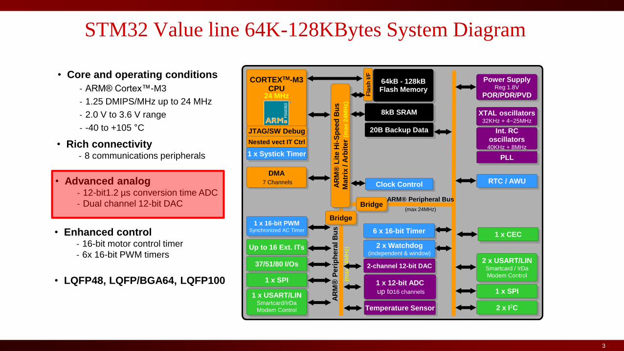
• Core and operating conditions
- ARM® Cortex™-M3
- 1.25 DMIPS/MHz up to 24 MHz
- 2.0 V to 3.6 V range
- -40 to +105 °C
• LQFP48, LQFP/BGA64, LQFP100
• Advanced analog- 12-bit1.2 µs conversion time ADC
- Dual channel 12-bit DAC
• Enhanced control- 16-bit motor control timer
- 6x 16-bit PWM timers
• Rich connectivity- 8 communications peripherals
STM32 Value line 64K-128KBytes System Diagram

4
Sensors
4
Integrated 9DoF IMU (Invensense)
Low-power cameras (Centeye, Awaiba, SoftKinetic)
IR sensors (LEAP, PMD)
EF sensors (Microchip GestIC, Plessy sensors)
ECG contactless (EPIC from Plessey) and bio sensors
Multi-Gas sensors
Contactless Voltage + Current
Acoustic sensors (MEMS, Analog, Digital)
Grove Starter Kit for LaunchPad
5
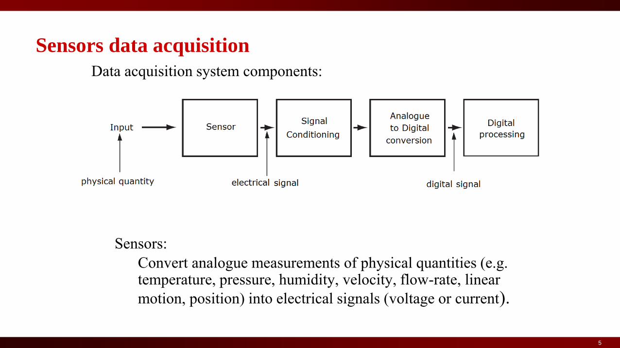
Sensors data acquisition
Data acquisition system components:
Sensors:
Convert analogue measurements of physical quantities (e.g. temperature, pressure, humidity, velocity, flow-rate, linear
motion, position) into electrical signals (voltage or current).

6
Data acquisition system components
Signal conditioning (filtering and amplification):- The operations required to convert the measured analogue signal to the
electrical signal range of the analogue-to-digital converter (ADC) may involve filtering, amplification, attenuation or impedance transformation.
Analogue-to-Digital Converter (ADC):- Input: Signal to be measured;
- Output: A digital code compatible with the digital processing system;
- Requires:
• Sample-and-hold: Used to take a snapshot of the continuously changinginput signal and maintain the value over the sample interval set by a clocksystem;
• A sampling frequency based on the Nyquist theorem.

7
ADC conversion Sample and Hold
Sample and Hold circuit does the signal time quantization
Restriction to digital information processing.
Known digital computers can only process discrete time series
Sample and hold-devices.
Ideally: width of clock pulse 0
Convert signal function in a series of value

8
Analogue-to-Digital Converter (ADC)
The ADC takes the voltage from the acquisition system (after signal conditioning) and converts it to an equivalent digital code;
ADC architectures: Successive Approximation (SAR)
Sigma Delta (SD or )
Slope or Dual Slope
Pipeline
Flash
ADC ideal transfer function
ADC performance

9
ADC performance
Resolution, R:
The resolution specifies the width of the digital output word;
- 10, 12, 16 Bit ADC
The width of the word implies the smallest change to the analogue voltage that
can be converted into a digital code;
The Least Significant Bit (LSB):
Accuracy:
Degree of conformity of a digital code representing the analogue
voltage to
Speed:
Maximum output data rate expressed in sample per second (sps)
n
ref
LSB
VV
2
10
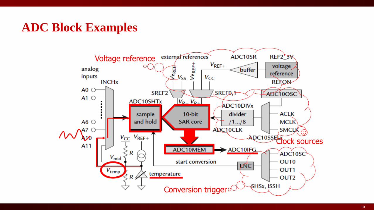
ADC Block Examples
Voltage reference
Clock sources
Conversion trigger

11
ADC Features
3 ADCs : ADC1 (master), ADC2 and ADC3 (slaves)
Maximum frequency of the ADC analog clock is 36MHz.
12-bits, 10-bits, 8-bits or 6-bits configurable resolution.
ADC conversion rate with 12 bit resolution is up to:
2.4 M.sample/s in single ADC mode,
4.5 M.sample/s in dual interleaved ADC mode,
7.2 M.sample/s in triple interleaved ADC mode.
Conversion range: 0 to 3.6 V.
ADC supply requirement: VDDA = 2.4V to 3.6V at full speed and down to 1.65V
at lower speed.
Up to 24 external channels.
3 ADC1 internal channels connected to:
Temperature sensor,
Internal voltage reference : VREFINT (1.2V typ),
VBAT for internal battery monitoring.

12
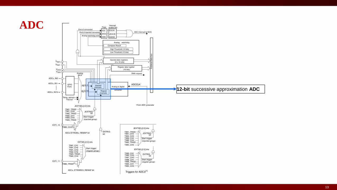
ADC – Summary and examples
• The 12-bit ADC is a successive approximation analog-to-digital converter. It has up to 18 multiplexed channels allowing it
measure signals from 16 external and two internal sources.
• A/D conversion of the various channels can be performed in single, continuous, scan or discontinuous mode. The result of
the ADC is stored in a left-aligned or right-aligned 16-bit data register.
• The analog watchdog feature allows the application to detect if the input voltage goes outside the user-defined high or low
thresholds.
• The ADC input clock is generated from the PCLK2 clock divided by a prescaler.
13
12-bit successive approximation ADC
ADC

14
Tconv = n * TCK
Successive Approximation ADC

15
Analog references / supply
ADC

16
The ADCCLK clock provided by the
Clock Controller is synchronous with
the PCLK2 (APB2 clock). The RCC
controller has a dedicated
programmable prescaler for the ADC
clock
If prescaler == 0 on the STM32
discovery ADCCLK==36MHz
ADC

17
RCC – Real Time Clock Control
18
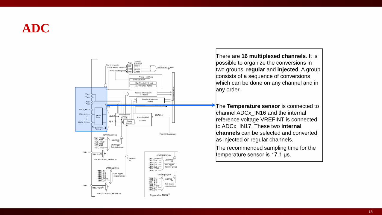
There are 16 multiplexed channels. It is
possible to organize the conversions in
two groups: regular and injected. A group
consists of a sequence of conversions
which can be done on any channel and in
any order.
The Temperature sensor is connected to
channel ADCx_IN16 and the internal
reference voltage VREFINT is connected
to ADCx_IN17. These two internal
channels can be selected and converted
as injected or regular channels.
The recommended sampling time for the
temperature sensor is 17.1 μs.
ADC

19
Conversion can be triggered by an external
event (e.g. timer capture, EXTI line)
ADC
20
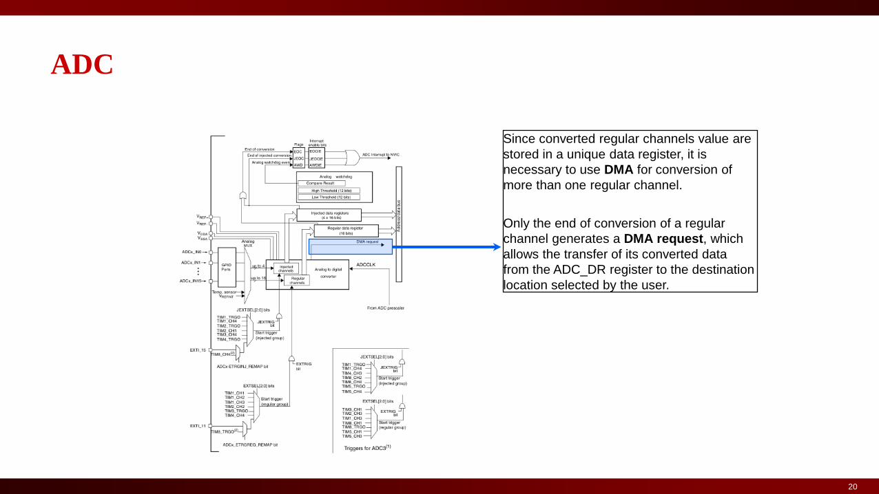
Since converted regular channels value are
stored in a unique data register, it is
necessary to use DMA for conversion of
more than one regular channel.
Only the end of conversion of a regular
channel generates a DMA request, which
allows the transfer of its converted data
from the ADC_DR register to the destination
location selected by the user.
ADC

21
When the conversion is done, data is
stored in 16 bits registers and the proper
flags are set to indicate the end of
conversion
ADC

22
ADC speed performances
AHB_PRESC
/1,2,..512
APB2_PRESC
/1, 2, 4, 8,16
ADC_PRESC
/2,4, 6, 8
ADC_CLK
(36MHz max)
AHBCLK
(168MHz max)
(1). ADC_PRESC = /2
(2). ADC_PRESC = /4
(a)APB_PRESC = /2
(b)APB_PRESC = /1
SYSCLK
(168MHz max)
APB2CLK
(84MHz max)
AHBCLK APB2CLK ADC_CLK ADC speed(15 cycles)
168MHz (a)84MHz
(2)21MHz
0.714μs1.4 Msample/s
144MHz (a)72MHz
(1)36MHz
0.416μs2.4 Msample/s
120MHz (a)60MHz
(1)30MHz
0.5μs2 Msample/s
96MHz (a)48MHz
(1)24MHz
0.625μs1.6 Msample/s
72MHz (b)72MHz
(1)36MHz
0.416μs2.4 Msample/s
23
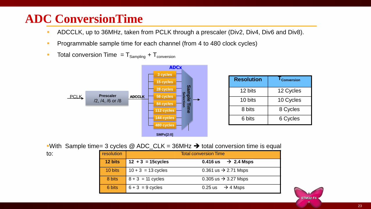
ADCCLK, up to 36MHz, taken from PCLK through a prescaler (Div2, Div4, Div6 and Div8).
Programmable sample time for each channel (from 4 to 480 clock cycles)
Total conversion Time = TSampling + Tconversion
ADCx
112 cycles
144 cycles
480 cycles
SMPx[2:0]
With Sample time= 3 cycles @ ADC_CLK = 36MHz total conversion time is equal
to:
ADC ConversionTime
ADCCLKPrescaler
/2, /4, /6 or /8PCLK
3 cycles
15 cycles
28 cycles
84 cycles
58 cycles
Sa
mp
leT
ime
Se
lec
tion
Resolution TConversion
12 bits 12 Cycles
10 bits 10 Cycles
8 bits 8 Cycles
6 bits 6 Cycles
resolution Total conversion Time
12 bits 12 + 3 = 15cycles 0.416 us 2.4 Msps
10 bits 10 + 3 = 13 cycles 0.361 us 2.71 Msps
8 bits 8 + 3 = 11 cycles 0.305 us 3.27 Msps
6 bits 6 + 3 = 9 cycles 0.25 us 4 Msps
24
Analog peripherals in STM33: Comparators
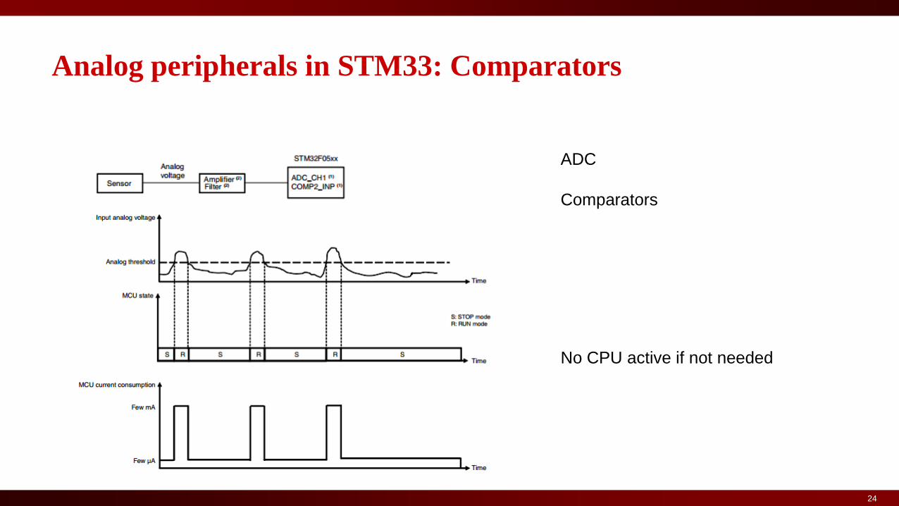
No CPU active if not needed
ADC
Comparators

25
Comparator 1 features 25
• Non-inverting input selectable from 24 I/Os
• Selectable edge detection through EXTI Line 21
• COMP1 and ADC can’t be used at same time since they share the ADC switch matrix
VSS
CH25
CH24
CH23
CH4
ADC
VCOMP
VREFINT
1.22V
VDD
10K400K
10K400K
+
-
COMP1
CH5
CH22
Temp. Sensor *
VREFINT *
Group 8
Group 1
Group 9
Group 7
Group 3
Group 2
CH10
CH11
CH12
CH13
CH1
CH2
CH3
CH0
CH14
CH15
CH19
CH20
CH21
CH9
CH8
CH6
CH7
CH18
ADC Switch matrix
EXTI 21
CMP1OUT
Routing Interface
PC0
PC1
PC2
PC3
PA0
PA1
PA2
PA3
PA6
PA7
PC4
PC5
PB12
PB13
PB14
PB15
PB0
PB1
PA4
PA5
PE7
PE8
PE9
PE10
26
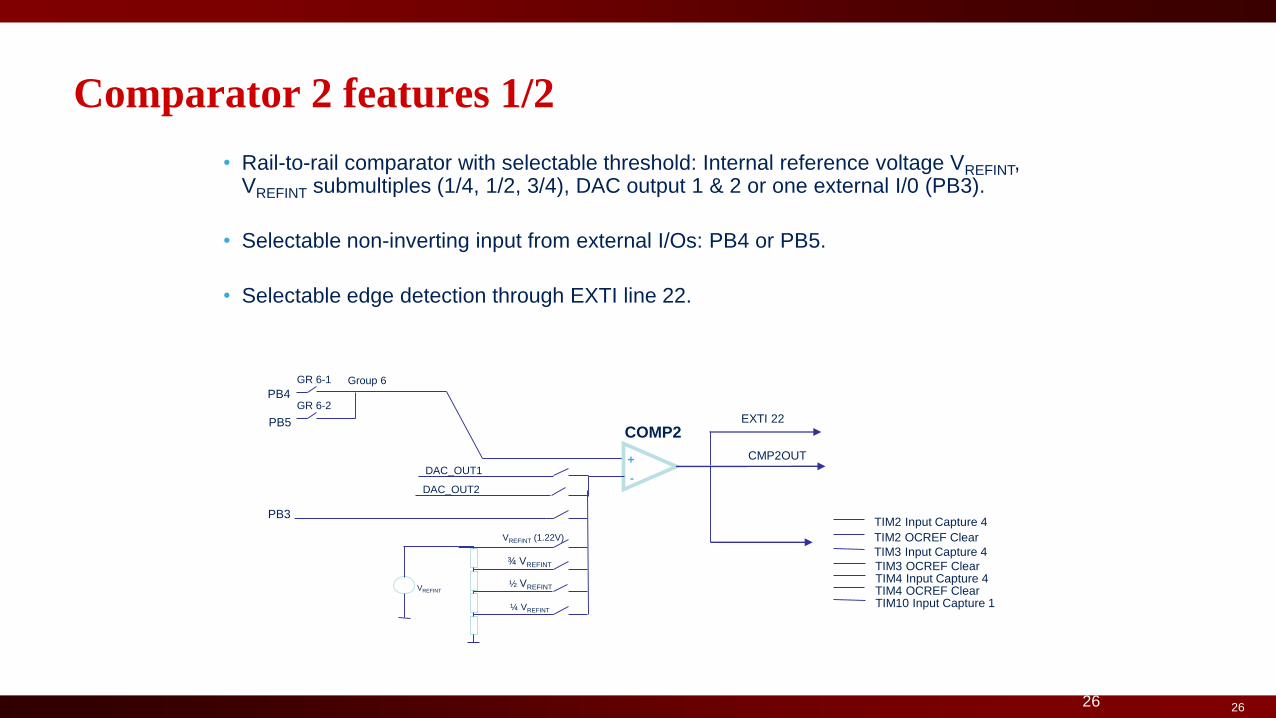
Comparator 2 features 1/2 26
• Rail-to-rail comparator with selectable threshold: Internal reference voltage VREFINT, VREFINT submultiples (1/4, 1/2, 3/4), DAC output 1 & 2 or one external I/0 (PB3).
• Selectable non-inverting input from external I/Os: PB4 or PB5.
• Selectable edge detection through EXTI line 22.
Group 6GR 6-1
GR 6-2
PB3
TIM3 OCREF Clear
TIM3 Input Capture 4
TIM2 OCREF Clear
TIM2 Input Capture 4
TIM4 Input Capture 4TIM4 OCREF ClearTIM10 Input Capture 1
DAC_OUT1
VREFINT (1.22V)
-
+
¾ VREFINT
½ VREFINT
¼ VREFINT
PB4
PB5 EXTI 22
COMP2
DAC_OUT2
VREFINT
CMP2OUT
26

27
Comparator 2 features 2/2 27
Group 6GR 6-1
GR 6-2
PB3
DAC_OUT1
VREFINT (1.22V)
-
+
¾ VREFINT
½ VREFINT
¼ VREFINT
PB4
PB5 EXTI 22
COMP2
DAC_OUT2
VREFINT
CMP2OUT
27
• COMP2 output can be redirected to:
• Timer input captures for pulse width or signal frequency measurements
• Timer output compare reference clear signal “OCREFCLR”, putting the PWM signal in safe state as soon as analog input voltage crosses the reference.
TIM2 IC4
TIM2 OCRECLR
TIM3 IC4
TIM3 OCREFCLR
TIM4 IC4
TIM4 OCRECLR
TIM10 IC1
OUTSEL[2:0]
28
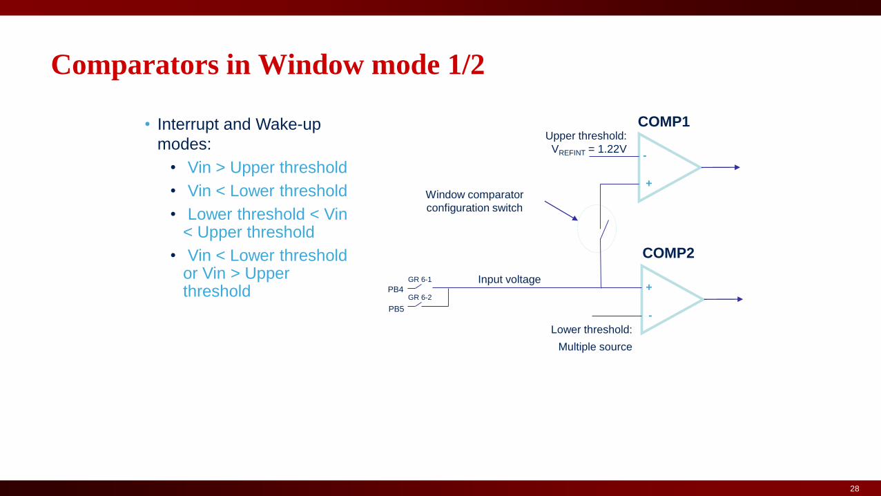
Comparators in Window mode 1/2 28
• Interrupt and Wake-up
modes:
• Vin > Upper threshold
• Vin < Lower threshold
• Lower threshold < Vin < Upper threshold
• Vin < Lower threshold or Vin > Upper threshold
Lower threshold:
Multiple source
+
-
-
+
Upper threshold:
VREFINT = 1.22V
Window comparator
configuration switch
Input voltage
COMP2
COMP1
PB4
PB5
GR 6-1
GR 6-2
30
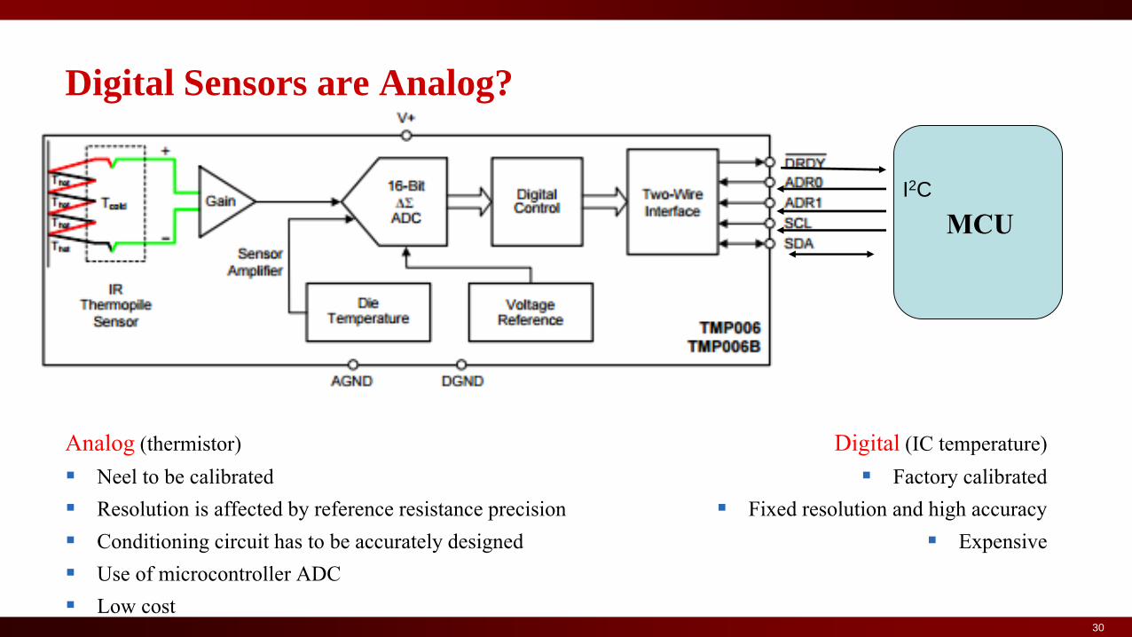
Digital Sensors are Analog?
MCU
I2C
Analog (thermistor)
Neel to be calibrated
Resolution is affected by reference resistance precision
Conditioning circuit has to be accurately designed
Use of microcontroller ADC
Low cost
Digital (IC temperature)
Factory calibrated
Fixed resolution and high accuracy
Expensive

31
Direct Memory Access - DMA

32
DMA Characteristics
Direct memory access (DMA) is used to provide high-speed data transfer between peripherals and
memory as well as memory to memory.
Data can be quickly moved by DMA without any CPU actions.
It keeps CPU resources free for other operations.
DATA TRANSFERS:
• With CPU:
• ldr
• str
• …
• ldr
• Str
• With DMA:
• Give the start command
• Wait the interrupt when transfer is completed

33
DMA in STM32F4
The two DMA controllers have 16 streams in total (8 for DMA1 and 8 for DMA2), each stream has
8 different channels each dedicated to managing memory access requests from one
peripheral. It has an arbiter for handling the priority between DMA requests.
• 16 streams for dedicated hardware DMA requests,
software trigger is also supported. The
configuration is done by software.
• 4 priority levels (very high, high, medium, low) or
hardware in case of equality (request 1 has priority
over request 2, etc.)
• Independent source and destination transfer size
(byte, half word, word), Source/destination
addresses must be aligned on the data size.
• 5 event flags (DMA Half Transfer, DMA Transfer
complete, DMA Transfer Error, DMA FIFO Error,
Direct Mode Error) logically ORed together in a
single interrupt request for each stream

34
DMA transfer modes: memory-to-memory, peripheral-to-memory, memory-to-
peripheral.
• Memory-to-Memory:
- Transfer data from one memory buffer to another
- Circular and Direct modes are not allowed.
- Only the DMA2 controller is able to perform memory-to-memory transfers
DMA Memory to memory

35
DMA Memory and peripherals
• Memory-to-Peripheral or Peripheral-to-Memory:
- When the threshold level of the FIFO is reached, its content is drained and stored into the
destination.
- Direct Mode: the threshold level of the FIFO is not used. After each single data transfer from
the peripheral to the FIFO, the data is immediately drained and stored into the destination.
Memory-to-Peripheral Peripheral-to-Memory
36
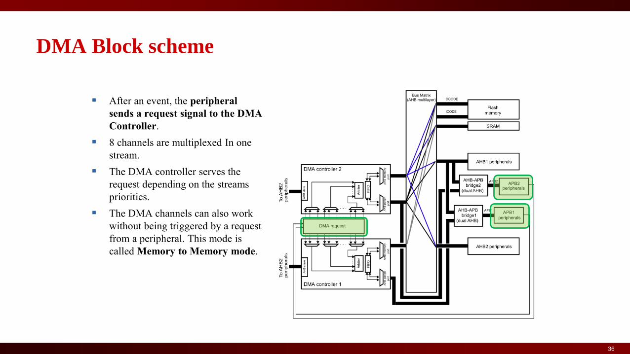
DMA Block scheme
After an event, the peripheral
sends a request signal to the DMA
Controller.
8 channels are multiplexed In one
stream.
The DMA controller serves the
request depending on the streams
priorities.
The DMA channels can also work
without being triggered by a request
from a peripheral. This mode is
called Memory to Memory mode.

37
DMA Block scheme
• DMA requests are collected and
channel multiplexed.
• The arbiter manages the stream
requests based on their priority and
launches the peripheral/memory
access sequences.
• The priorities are managed in two
stages:
- Software (defined priority)
- Hardware (if 2 requests have
the same software priority
level, the channel with the
lowest number will get priority
versus the channel with the
highest number.)

38
DMA Block scheme
• Each channel can handle DMA
transfers between a peripheral
register located at a fixed address
and a memory address.
• Peripheral and memory pointers can
optionally be automatically post-
incremented after each transaction.
• If incremented mode is enabled, the
address of the next transfer will be
the address of the previous one
incremented by 1, 2 or 4 depending
on the chosen data size.

39
DMA Block scheme
• Noncircular mode: no DMA
request is served after the last
transfer (that is once the number of
data items to be transferred has
reached zero).
• Circular mode: handle circular
buffers and continuous data flows
(e.g. ADC scan mode). When
circular mode is activated, the
number of data to be transferred is
automatically reloaded with the
initial value programmed during the
channel configuration phase, and the
DMA requests continue to be served.

40
DMA Channels
Each Stream is multiplexed up to eight channel, only one channel at a time can be active
It is not possible to activate two channels on the same stream
Is possible to perform transfers from all 8 streams

41
Code example

• We want to use a DMA and ADC to sample a signal from an input
channel.
• Configure and enable DMA
1. Configure and enable ADC
1. Configure the prescaler for ADCCLK
2. Configure and init the ADC (conversion mode, sampling time,
etc...)
3. Calibrate ADC
4. Starting the acquisition
ADC

1. Configure and enable DMA
#define ADCx_DR_Address ((uint32_t)0x4001204C)
DMA_InitTypeDef DMA_InitStructure;
/* Enable DMA2 clock*/
RCC_AHB1PeriphClockCmd(RCC_AHB1Periph_DMA2, ENABLE);
/* DMA2 Stream0 channel 0 configuration */
DMA_InitStructure.DMA_Channel = DMA_Channel_0;
DMA_InitStructure.DMA_PeripheralBaseAddr = (uint32_t)&ADC1->DR;
DMA_InitStructure.DMA_Memory0BaseAddr = (uint32_t)&ADC1ConvertedValue;
DMA_InitStructure.DMA_DIR = DMA_DIR_PeripheralToMemory;
DMA_InitStructure.DMA_BufferSize = 1;
DMA_InitStructure.DMA_PeripheralInc = DMA_PeripheralInc_Disable;
DMA_InitStructure.DMA_MemoryInc = DMA_MemoryInc_Disable;
DMA_InitStructure.DMA_PeripheralDataSize = DMA_PeripheralDataSize_HalfWord;
DMA_InitStructure.DMA_MemoryDataSize = DMA_MemoryDataSize_HalfWord;
DMA_InitStructure.DMA_Mode = DMA_Mode_Circular;
DMA_InitStructure.DMA_Priority = DMA_Priority_High;
DMA_InitStructure.DMA_FIFOMode = DMA_FIFOMode_Disable;
DMA_InitStructure.DMA_FIFOThreshold = DMA_FIFOThreshold_HalfFull;
DMA_InitStructure.DMA_MemoryBurst = DMA_MemoryBurst_Single;
DMA_InitStructure.DMA_PeripheralBurst = DMA_PeripheralBurst_Single;
DMA_Init(DMA2_Stream0, &DMA_InitStructure);
/* Enable DMA1 channel0 */DMA_Cmd(DMA2_Stream0, ENABLE);
Address of the register where the result
of the acquisition is saved
ADC

1. Configure and enable DMA
#define ADCx_DR_Address ((uint32_t)0x4001204C)
DMA_InitTypeDef DMA_InitStructure;
/* Enable DMA2 clock*/
RCC_AHB1PeriphClockCmd(RCC_AHB1Periph_DMA2, ENABLE);
/* DMA2 Stream0 channel 0 configuration */
DMA_InitStructure.DMA_Channel = DMA_Channel_0;
DMA_InitStructure.DMA_PeripheralBaseAddr = (uint32_t)&ADC1->DR;
DMA_InitStructure.DMA_Memory0BaseAddr = (uint32_t)&ADC1ConvertedValue;
DMA_InitStructure.DMA_DIR = DMA_DIR_PeripheralToMemory;
DMA_InitStructure.DMA_BufferSize = 1;
DMA_InitStructure.DMA_PeripheralInc = DMA_PeripheralInc_Disable;
DMA_InitStructure.DMA_MemoryInc = DMA_MemoryInc_Disable;
DMA_InitStructure.DMA_PeripheralDataSize = DMA_PeripheralDataSize_HalfWord;
DMA_InitStructure.DMA_MemoryDataSize = DMA_MemoryDataSize_HalfWord;
DMA_InitStructure.DMA_Mode = DMA_Mode_Circular;
DMA_InitStructure.DMA_Priority = DMA_Priority_High;
DMA_InitStructure.DMA_FIFOMode = DMA_FIFOMode_Disable;
DMA_InitStructure.DMA_FIFOThreshold = DMA_FIFOThreshold_HalfFull;
DMA_InitStructure.DMA_MemoryBurst = DMA_MemoryBurst_Single;
DMA_InitStructure.DMA_PeripheralBurst = DMA_PeripheralBurst_Single;
DMA_Init(DMA2_Stream0, &DMA_InitStructure);
/* Enable DMA1 channel0 */DMA_Cmd(DMA2_Stream0, ENABLE);
ADC
We read 16bits from ADC and save
16bits in the ADC1ConvertedValue variable

2. Configure and enable ADC
ADC_InitTypeDef ADC_InitStructure;
ADC_CommonInitTypeDef ADC_CommonInitStructure;
/* Enable ADC1 clock*/
RCC_APB2PeriphClockCmd(RCC_APB2Periph_ADC1, ENABLE);
/* ADC Common Init */
ADC_CommonInitStructure.ADC_Mode = ADC_Mode_Independent;
ADC_CommonInitStructure.ADC_Prescaler = ADC_Prescaler_Div2;
ADC_CommonInitStructure.ADC_DMAAccessMode = ADC_DMAAccessMode_Disabled;
ADC_CommonInitStructure.ADC_TwoSamplingDelay = ADC_TwoSamplingDelay_5Cycles;
ADC_CommonInit(&ADC_CommonInitStructure);
/* ADC1 Init */
ADC_InitStructure.ADC_Resolution = ADC_Resolution_12b;
ADC_InitStructure.ADC_ScanConvMode = DISABLE;
ADC_InitStructure.ADC_ContinuousConvMode = ENABLE;
ADC_InitStructure.ADC_ExternalTrigConvEdge = ADC_ExternalTrigConvEdge_None;
ADC_InitStructure.ADC_ExternalTrigConv = ADC_ExternalTrigConv_T1_CC1;
ADC_InitStructure.ADC_DataAlign = ADC_DataAlign_Right;
ADC_InitStructure.ADC_NbrOfConversion = 1;
ADC_Init(ADC1, &ADC_InitStructure);
/* ADC1 regular channel12 configuration */
ADC_RegularChannelConfig(ADC1, ADC_Channel_12, 1, ADC_SampleTime_3Cycles);
/* Enable DMA request after last transfer (Single-ADC mode) */
ADC_DMARequestAfterLastTransferCmd(ADC1, ENABLE);
/* Enable ADC1 DMA */
ADC_DMACmd(ADC1, ENABLE);
/* Enable ADC1 */
ADC_Cmd(ADC1, ENABLE);
ADC
ADC in independent mode

2. Configure and enable ADC
ADC_InitTypeDef ADC_InitStructure;
ADC_CommonInitTypeDef ADC_CommonInitStructure;
/* Enable ADC1 clock*/
RCC_APB2PeriphClockCmd(RCC_APB2Periph_ADC1, ENABLE);
/* ADC Common Init */
ADC_CommonInitStructure.ADC_Mode = ADC_Mode_Independent;
ADC_CommonInitStructure.ADC_Prescaler = ADC_Prescaler_Div2;
ADC_CommonInitStructure.ADC_DMAAccessMode = ADC_DMAAccessMode_Disabled;
ADC_CommonInitStructure.ADC_TwoSamplingDelay = ADC_TwoSamplingDelay_5Cycles;
ADC_CommonInit(&ADC_CommonInitStructure);
/* ADC1 Init */
ADC_InitStructure.ADC_Resolution = ADC_Resolution_12b;
ADC_InitStructure.ADC_ScanConvMode = DISABLE;
ADC_InitStructure.ADC_ContinuousConvMode = ENABLE;
ADC_InitStructure.ADC_ExternalTrigConvEdge = ADC_ExternalTrigConvEdge_None;
ADC_InitStructure.ADC_ExternalTrigConv = ADC_ExternalTrigConv_T1_CC1;
ADC_InitStructure.ADC_DataAlign = ADC_DataAlign_Right;
ADC_InitStructure.ADC_NbrOfConversion = 1;
ADC_Init(ADC1, &ADC_InitStructure);
/* ADC1 regular channel12 configuration */
ADC_RegularChannelConfig(ADC1, ADC_Channel_12, 1, ADC_SampleTime_3Cycles);
/* Enable DMA request after last transfer (Single-ADC mode) */
ADC_DMARequestAfterLastTransferCmd(ADC1, ENABLE);
/* Enable ADC1 DMA */
ADC_DMACmd(ADC1, ENABLE);
/* Enable ADC1 */
ADC_Cmd(ADC1, ENABLE);
ADC
Set the prescaler to have ADCCLK==18MHz

2. Configure and enable ADC
ADC_InitTypeDef ADC_InitStructure;
ADC_CommonInitTypeDef ADC_CommonInitStructure;
/* Enable ADC1 clock*/
RCC_APB2PeriphClockCmd(RCC_APB2Periph_ADC1, ENABLE);
/* ADC Common Init */
ADC_CommonInitStructure.ADC_Mode = ADC_Mode_Independent;
ADC_CommonInitStructure.ADC_Prescaler = ADC_Prescaler_Div2;
ADC_CommonInitStructure.ADC_DMAAccessMode = ADC_DMAAccessMode_Disabled;
ADC_CommonInitStructure.ADC_TwoSamplingDelay = ADC_TwoSamplingDelay_5Cycles;
ADC_CommonInit(&ADC_CommonInitStructure);
/* ADC1 Init */
ADC_InitStructure.ADC_Resolution = ADC_Resolution_12b;
ADC_InitStructure.ADC_ScanConvMode = DISABLE;
ADC_InitStructure.ADC_ContinuousConvMode = ENABLE;
ADC_InitStructure.ADC_ExternalTrigConvEdge = ADC_ExternalTrigConvEdge_None;
ADC_InitStructure.ADC_ExternalTrigConv = ADC_ExternalTrigConv_T1_CC1;
ADC_InitStructure.ADC_DataAlign = ADC_DataAlign_Right;
ADC_InitStructure.ADC_NbrOfConversion = 1;
ADC_Init(ADC1, &ADC_InitStructure);
/* ADC1 regular channel12 configuration */
ADC_RegularChannelConfig(ADC1, ADC_Channel_12, 1, ADC_SampleTime_3Cycles);
/* Enable DMA request after last transfer (Single-ADC mode) */
ADC_DMARequestAfterLastTransferCmd(ADC1, ENABLE);
/* Enable ADC1 DMA */
ADC_DMACmd(ADC1, ENABLE);
/* Enable ADC1 */
ADC_Cmd(ADC1, ENABLE);
ADC
ADC in Continuous Mode
2. Configure and enable ADC
ADC_InitTypeDef ADC_InitStructure;
ADC_CommonInitTypeDef ADC_CommonInitStructure;
/* Enable ADC1 clock*/
RCC_APB2PeriphClockCmd(RCC_APB2Periph_ADC1, ENABLE);
/* ADC Common Init */
ADC_CommonInitStructure.ADC_Mode = ADC_Mode_Independent;
ADC_CommonInitStructure.ADC_Prescaler = ADC_Prescaler_Div2;
ADC_CommonInitStructure.ADC_DMAAccessMode = ADC_DMAAccessMode_Disabled;
ADC_CommonInitStructure.ADC_TwoSamplingDelay = ADC_TwoSamplingDelay_5Cycles;
ADC_CommonInit(&ADC_CommonInitStructure);
/* ADC1 Init */
ADC_InitStructure.ADC_Resolution = ADC_Resolution_12b;
ADC_InitStructure.ADC_ScanConvMode = DISABLE;
ADC_InitStructure.ADC_ContinuousConvMode = ENABLE;
ADC_InitStructure.ADC_ExternalTrigConvEdge = ADC_ExternalTrigConvEdge_None;
ADC_InitStructure.ADC_ExternalTrigConv = ADC_ExternalTrigConv_T1_CC1;
ADC_InitStructure.ADC_DataAlign = ADC_DataAlign_Right;
ADC_InitStructure.ADC_NbrOfConversion = 1;
ADC_Init(ADC1, &ADC_InitStructure);
/* ADC1 regular channel12 configuration */
ADC_RegularChannelConfig(ADC1, ADC_Channel_12, 1, ADC_SampleTime_3Cycles);
/* Enable DMA request after last transfer (Single-ADC mode) */
ADC_DMARequestAfterLastTransferCmd(ADC1, ENABLE);
/* Enable ADC1 DMA */
ADC_DMACmd(ADC1, ENABLE);
/* Enable ADC1 */
ADC_Cmd(ADC1, ENABLE);
ADC
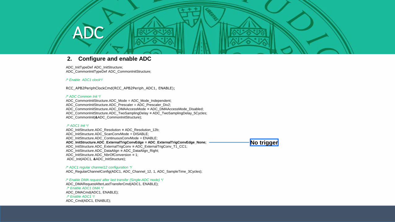
No trigger

2. Configure and enable ADC
ADC_InitTypeDef ADC_InitStructure;
ADC_CommonInitTypeDef ADC_CommonInitStructure;
/* Enable ADC1 clock*/
RCC_APB2PeriphClockCmd(RCC_APB2Periph_ADC1, ENABLE);
/* ADC Common Init */
ADC_CommonInitStructure.ADC_Mode = ADC_Mode_Independent;
ADC_CommonInitStructure.ADC_Prescaler = ADC_Prescaler_Div2;
ADC_CommonInitStructure.ADC_DMAAccessMode = ADC_DMAAccessMode_Disabled;
ADC_CommonInitStructure.ADC_TwoSamplingDelay = ADC_TwoSamplingDelay_5Cycles;
ADC_CommonInit(&ADC_CommonInitStructure);
/* ADC1 Init */
ADC_InitStructure.ADC_Resolution = ADC_Resolution_12b;
ADC_InitStructure.ADC_ScanConvMode = DISABLE;
ADC_InitStructure.ADC_ContinuousConvMode = ENABLE;
ADC_InitStructure.ADC_ExternalTrigConvEdge = ADC_ExternalTrigConvEdge_None;
ADC_InitStructure.ADC_ExternalTrigConv = ADC_ExternalTrigConv_T1_CC1;
ADC_InitStructure.ADC_DataAlign = ADC_DataAlign_Right;
ADC_InitStructure.ADC_NbrOfConversion = 1;
ADC_Init(ADC1, &ADC_InitStructure);
/* ADC1 regular channel12 configuration */
ADC_RegularChannelConfig(ADC1, ADC_Channel_12, 1, ADC_SampleTime_3Cycles);
/* Enable DMA request after last transfer (Single-ADC mode) */
ADC_DMARequestAfterLastTransferCmd(ADC1, ENABLE);
/* Enable ADC1 DMA */
ADC_DMACmd(ADC1, ENABLE);
/* Enable ADC1 */
ADC_Cmd(ADC1, ENABLE);
ADC
Number of Conversion
2. Configure and enable ADC
ADC_InitTypeDef ADC_InitStructure;
ADC_CommonInitTypeDef ADC_CommonInitStructure;
/* Enable ADC1 clock*/
RCC_APB2PeriphClockCmd(RCC_APB2Periph_ADC1, ENABLE);
/* ADC Common Init */
ADC_CommonInitStructure.ADC_Mode = ADC_Mode_Independent;
ADC_CommonInitStructure.ADC_Prescaler = ADC_Prescaler_Div2;
ADC_CommonInitStructure.ADC_DMAAccessMode = ADC_DMAAccessMode_Disabled;
ADC_CommonInitStructure.ADC_TwoSamplingDelay = ADC_TwoSamplingDelay_5Cycles;
ADC_CommonInit(&ADC_CommonInitStructure);
/* ADC1 Init */
ADC_InitStructure.ADC_Resolution = ADC_Resolution_12b;
ADC_InitStructure.ADC_ScanConvMode = DISABLE;
ADC_InitStructure.ADC_ContinuousConvMode = ENABLE;
ADC_InitStructure.ADC_ExternalTrigConvEdge = ADC_ExternalTrigConvEdge_None;
ADC_InitStructure.ADC_ExternalTrigConv = ADC_ExternalTrigConv_T1_CC1;
ADC_InitStructure.ADC_DataAlign = ADC_DataAlign_Right;
ADC_InitStructure.ADC_NbrOfConversion = 1;
ADC_Init(ADC1, &ADC_InitStructure);
/* ADC1 regular channel12 configuration */
ADC_RegularChannelConfig(ADC1, ADC_Channel_12, 1, ADC_SampleTime_3Cycles);
/* Enable DMA request after last transfer (Single-ADC mode) */
ADC_DMARequestAfterLastTransferCmd(ADC1, ENABLE);
/* Enable ADC1 DMA */
ADC_DMACmd(ADC1, ENABLE);
/* Enable ADC1 */
ADC_Cmd(ADC1, ENABLE);
ADC
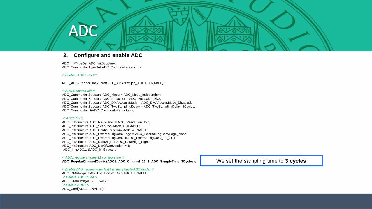
We set the sampling time to 3 cycles

2. Configure and enable ADC
ADC_InitTypeDef ADC_InitStructure;
ADC_CommonInitTypeDef ADC_CommonInitStructure;
/* Enable ADC1 clock*/
RCC_APB2PeriphClockCmd(RCC_APB2Periph_ADC1, ENABLE);
/* ADC Common Init */
ADC_CommonInitStructure.ADC_Mode = ADC_Mode_Independent;
ADC_CommonInitStructure.ADC_Prescaler = ADC_Prescaler_Div2;
ADC_CommonInitStructure.ADC_DMAAccessMode = ADC_DMAAccessMode_Disabled;
ADC_CommonInitStructure.ADC_TwoSamplingDelay = ADC_TwoSamplingDelay_5Cycles;
ADC_CommonInit(&ADC_CommonInitStructure);
/* ADC1 Init */
ADC_InitStructure.ADC_Resolution = ADC_Resolution_12b;
ADC_InitStructure.ADC_ScanConvMode = DISABLE;
ADC_InitStructure.ADC_ContinuousConvMode = ENABLE;
ADC_InitStructure.ADC_ExternalTrigConvEdge = ADC_ExternalTrigConvEdge_None;
ADC_InitStructure.ADC_ExternalTrigConv = ADC_ExternalTrigConv_T1_CC1;
ADC_InitStructure.ADC_DataAlign = ADC_DataAlign_Right;
ADC_InitStructure.ADC_NbrOfConversion = 1;
ADC_Init(ADC1, &ADC_InitStructure);
/* ADC1 regular channel12 configuration */
ADC_RegularChannelConfig(ADC1, ADC_Channel_12, 1, ADC_SampleTime_3Cycles);
/* Enable DMA request after last transfer (Single-ADC mode) */
ADC_DMARequestAfterLastTransferCmd(ADC1, ENABLE);
/* Enable ADC1 DMA */
ADC_DMACmd(ADC1, ENABLE);
/* Enable ADC1 */
ADC_Cmd(ADC1, ENABLE);
ADC
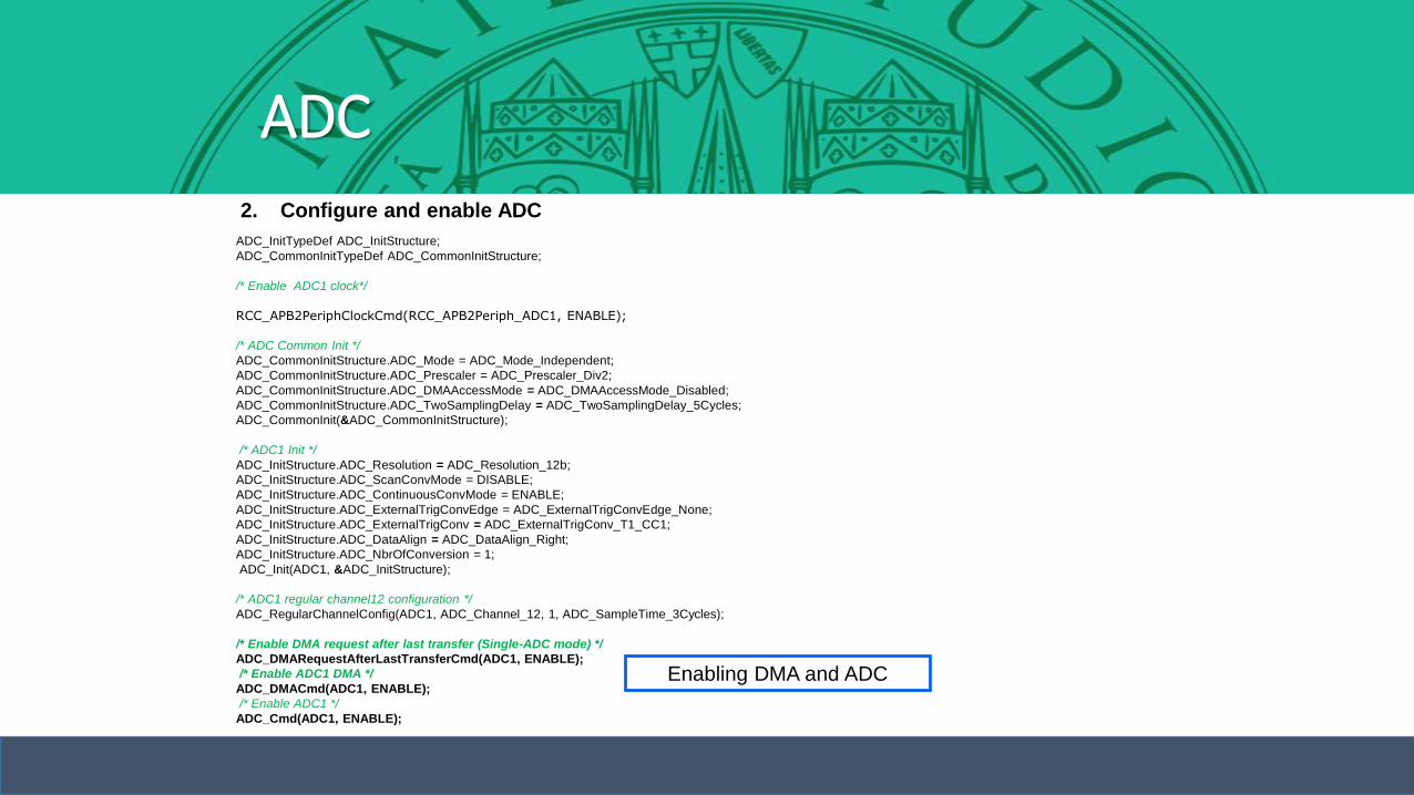
Enabling DMA and ADC
2. Configure and enable ADC
ADC_InitTypeDef ADC_InitStructure;
ADC_CommonInitTypeDef ADC_CommonInitStructure;
/* Enable ADC1 clock*/
RCC_APB2PeriphClockCmd(RCC_APB2Periph_ADC1, ENABLE);
/* ADC Common Init */
ADC_CommonInitStructure.ADC_Mode = ADC_Mode_Independent;
ADC_CommonInitStructure.ADC_Prescaler = ADC_Prescaler_Div2;
ADC_CommonInitStructure.ADC_DMAAccessMode = ADC_DMAAccessMode_Disabled;
ADC_CommonInitStructure.ADC_TwoSamplingDelay = ADC_TwoSamplingDelay_5Cycles;
ADC_CommonInit(&ADC_CommonInitStructure);
/* ADC1 Init */
ADC_InitStructure.ADC_Resolution = ADC_Resolution_12b;
ADC_InitStructure.ADC_ScanConvMode = DISABLE;
ADC_InitStructure.ADC_ContinuousConvMode = ENABLE;
ADC_InitStructure.ADC_ExternalTrigConvEdge = ADC_ExternalTrigConvEdge_None;
ADC_InitStructure.ADC_ExternalTrigConv = ADC_ExternalTrigConv_T1_CC1;
ADC_InitStructure.ADC_DataAlign = ADC_DataAlign_Right;
ADC_InitStructure.ADC_NbrOfConversion = 1;
ADC_Init(ADC1, &ADC_InitStructure);
/* ADC1 regular channel12 configuration */
ADC_RegularChannelConfig(ADC1, ADC_Channel_12, 1, ADC_SampleTime_3Cycles);
/* Enable DMA request after last transfer (Single-ADC mode) */
ADC_DMARequestAfterLastTransferCmd(ADC1, ENABLE);
/* Enable ADC1 DMA */
ADC_DMACmd(ADC1, ENABLE);
/* Enable ADC1 */
ADC_Cmd(ADC1, ENABLE);
ADC
Enabling DMA and ADC
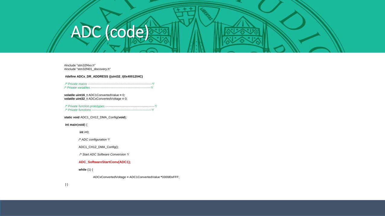
#include "stm32f4xx.h"
#include "stm32f401_discovery.h"
#define ADCx_DR_ADDRESS ((uint32_t)0x4001204C)
/* Private macro -------------------------------------------------------------*/
/* Private variables ---------------------------------------------------------*/
volatile uint16_t ADC1ConvertedValue = 0;
volatile uint32_t ADCxConvertedVoltage = 0;
/* Private function prototypes -----------------------------------------------*/
/* Private functions ---------------------------------------------------------*/
static void ADC1_CH12_DMA_Config(void);
int main(void) {
int i=0;
/* ADC configuration */
ADC1_CH12_DMA_Config();
/* Start ADC Software Conversion */
ADC_SoftwareStartConv(ADC1);
while (1) {
ADCxConvertedVoltage = ADC1ConvertedValue *3300/0xFFF;
} }
ADC (code)
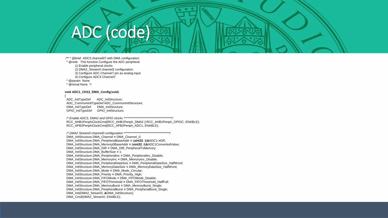
/** * @brief ADC3 channel07 with DMA configuration
* @note This function Configure the ADC peripheral
1) Enable peripheral clocks
2) DMA2_Stream0 channel2 configuration
3) Configure ADC Channel7 pin as analog input
4) Configure ADC3 Channel7
* @param None
* @retval None */
void ADC1_CH12_DMA_Config(void)
{
ADC_InitTypeDef ADC_InitStructure;
ADC_CommonInitTypeDef ADC_CommonInitStructure;
DMA_InitTypeDef DMA_InitStructure;
GPIO_InitTypeDef GPIO_InitStructure;
/* Enable ADC3, DMA2 and GPIO clocks ****************************************/
RCC_AHB1PeriphClockCmd(RCC_AHB1Periph_DMA2 | RCC_AHB1Periph_GPIOC, ENABLE);
RCC_APB2PeriphClockCmd(RCC_APB2Periph_ADC1, ENABLE);
/* DMA2 Stream0 channel0 configuration **************************************/
DMA_InitStructure.DMA_Channel = DMA_Channel_0;
DMA_InitStructure.DMA_PeripheralBaseAddr = (uint32_t)&ADC1->DR;
DMA_InitStructure.DMA_Memory0BaseAddr = (uint32_t)&ADC1ConvertedValue;
DMA_InitStructure.DMA_DIR = DMA_DIR_PeripheralToMemory;
DMA_InitStructure.DMA_BufferSize = 1;
DMA_InitStructure.DMA_PeripheralInc = DMA_PeripheralInc_Disable;
DMA_InitStructure.DMA_MemoryInc = DMA_MemoryInc_Disable;
DMA_InitStructure.DMA_PeripheralDataSize = DMA_PeripheralDataSize_HalfWord;
DMA_InitStructure.DMA_MemoryDataSize = DMA_MemoryDataSize_HalfWord;
DMA_InitStructure.DMA_Mode = DMA_Mode_Circular;
DMA_InitStructure.DMA_Priority = DMA_Priority_High;
DMA_InitStructure.DMA_FIFOMode = DMA_FIFOMode_Disable;
DMA_InitStructure.DMA_FIFOThreshold = DMA_FIFOThreshold_HalfFull;
DMA_InitStructure.DMA_MemoryBurst = DMA_MemoryBurst_Single;
DMA_InitStructure.DMA_PeripheralBurst = DMA_PeripheralBurst_Single;
DMA_Init(DMA2_Stream0, &DMA_InitStructure);
DMA_Cmd(DMA2_Stream0, ENABLE);
ADC (code)
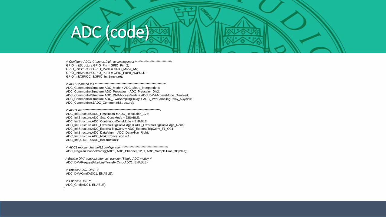
/* Configure ADC1 Channel12 pin as analog input ******************************/
GPIO_InitStructure.GPIO_Pin = GPIO_Pin_2;
GPIO_InitStructure.GPIO_Mode = GPIO_Mode_AN;
GPIO_InitStructure.GPIO_PuPd = GPIO_PuPd_NOPULL ;
GPIO_Init(GPIOC, &GPIO_InitStructure);
/* ADC Common Init **********************************************************/
ADC_CommonInitStructure.ADC_Mode = ADC_Mode_Independent;
ADC_CommonInitStructure.ADC_Prescaler = ADC_Prescaler_Div2;
ADC_CommonInitStructure.ADC_DMAAccessMode = ADC_DMAAccessMode_Disabled;
ADC_CommonInitStructure.ADC_TwoSamplingDelay = ADC_TwoSamplingDelay_5Cycles;
ADC_CommonInit(&ADC_CommonInitStructure);
/* ADC1 Init ****************************************************************/
ADC_InitStructure.ADC_Resolution = ADC_Resolution_12b;
ADC_InitStructure.ADC_ScanConvMode = DISABLE;
ADC_InitStructure.ADC_ContinuousConvMode = ENABLE;
ADC_InitStructure.ADC_ExternalTrigConvEdge = ADC_ExternalTrigConvEdge_None;
ADC_InitStructure.ADC_ExternalTrigConv = ADC_ExternalTrigConv_T1_CC1;
ADC_InitStructure.ADC_DataAlign = ADC_DataAlign_Right;
ADC_InitStructure.ADC_NbrOfConversion = 1;
ADC_Init(ADC1, &ADC_InitStructure);
/* ADC1 regular channel12 configuration *************************************/
ADC_RegularChannelConfig(ADC1, ADC_Channel_12, 1, ADC_SampleTime_3Cycles);
/* Enable DMA request after last transfer (Single-ADC mode) */
ADC_DMARequestAfterLastTransferCmd(ADC1, ENABLE);
/* Enable ADC1 DMA */
ADC_DMACmd(ADC1, ENABLE);
/* Enable ADC1 */
ADC_Cmd(ADC1, ENABLE);
}
ADC (code)
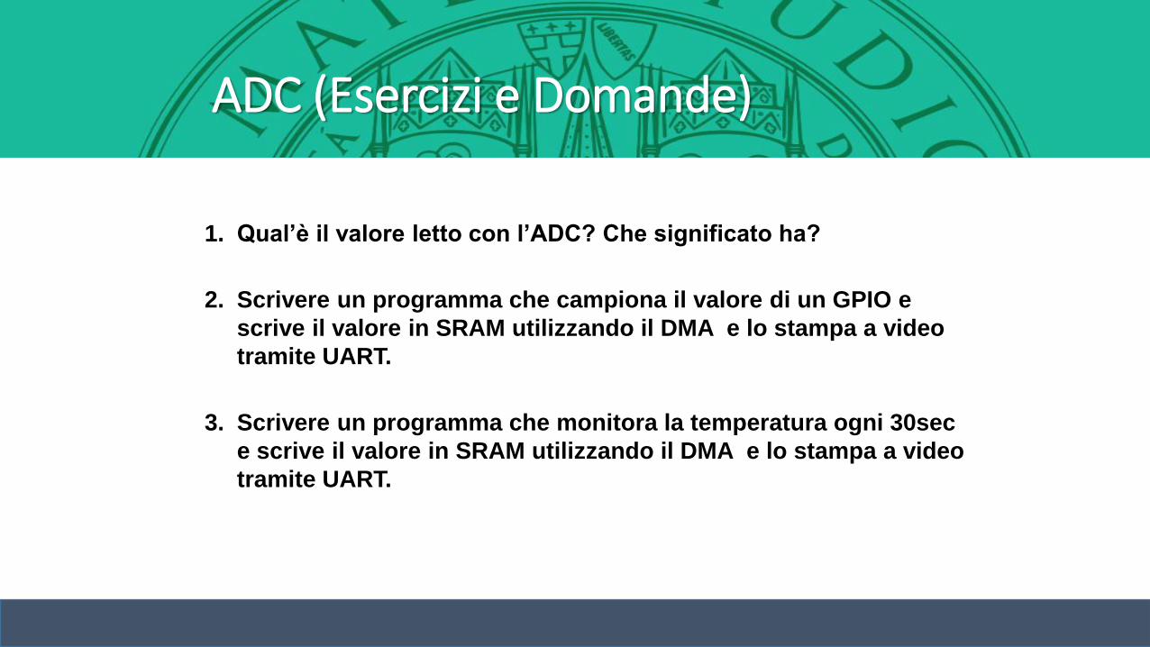
1. Qual’è il valore letto con l’ADC? Che significato ha?
2. Scrivere un programma che campiona il valore di un GPIO e
scrive il valore in SRAM utilizzando il DMA e lo stampa a video
tramite UART.
3. Scrivere un programma che monitora la temperatura ogni 30sec
e scrive il valore in SRAM utilizzando il DMA e lo stampa a video
tramite UART.
ADC (Esercizi e Domande)

Analog to Digital Conversion:
• Connect the potentiometer to the board:• 10K potentiometer
• External pin connected to 3.3V and GND
• Central pin connected to PC2
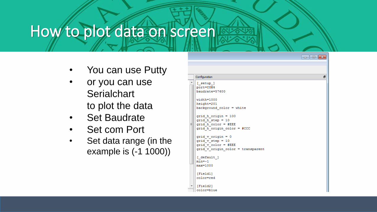
How to plot data on screen
• You can use Putty
• or you can use
Serialchart
to plot the data
• Set Baudrate
• Set com Port• Set data range (in the
example is (-1 1000))

How to plot data on screen
• Format data like in the example:
• Printf(“%d,%f,%f/r/n”,counter,data1,data2)