MICROCONTROLLERS Combinational Logic and … Portland State University MICROCONTROLLERS...
22
PH-315 Portland State University MICROCONTROLLERS Combinational Logic and PWM OBJECTIVE 1. Become familiar with binary coding (encoding and decoding). Since the Arduino microcontroller uses a C++ based programming language (where the Hexadecimal system is of standard use) we have to get familiar expressing binary numbers in hexadecimal (HEX) notation 1 2. Familiarize with the operational principle of the “7 Segment Display” and the “Dot Matrix Display”. 3. Use Pulse Width Modulation (PWM) to control the display brightness. 1. Introduction In combinational logic, the outputs of the circuit block are only determined by the logical function of their current input state. Combinational logic can be implemented by an Arduino in a ver easily. Y straightforward way. Fig 1. Illustration of combinational logic. The output is a function f of the input. In this lab, you will apply combinational logic strategies to implement different display schemes in “7 Segment Display” and “Dot Matrix Display” units. 2. The 7-segment Single-digit Display The seven segment display, consists of seven LEDs (hence its name) arranged in a rectangular fashion as shown in Fig. 2. Each of the seven LEDs is called a segment because when illuminated the segment forms part of a numerical digit (both Decimal and Hex) to be displayed. An additional 8th LED is sometimes used within the same package thus allowing the indication of a decimal point (DP). Each one of the seven LEDs in the display is given a positional segment with one of its connection pins being brought straight out of the rectangular plastic package. These individual LED pins are labelled from a to g, which connect to one terminal of the corresponding LED. The other LED pin terminals are wired together to a common pin. So by forward biasing the appropriate pins of the LED segments in a particular order, some segments will be light and
-
Upload
nguyentruc -
Category
Documents
-
view
217 -
download
3
Transcript of MICROCONTROLLERS Combinational Logic and … Portland State University MICROCONTROLLERS...

PH-315 Portland State University
MICROCONTROLLERS Combinational Logic and PWM
OBJECTIVE
1. Become familiar with binary coding (encoding and decoding). Since the Arduino
microcontroller uses a C++ based programming language (where the Hexadecimal
system is of standard use) we have to get familiar expressing binary numbers in
hexadecimal (HEX) notation1
2. Familiarize with the operational principle of the “7 Segment Display” and the “Dot
Matrix Display”.
3. Use Pulse Width Modulation (PWM) to control the display brightness.
1. Introduction In combinational logic, the outputs of the circuit block are only determined by the logical
function of their current input state. Combinational logic can be implemented by an Arduino in
a ver easily. Y straightforward way.
Fig 1. Illustration of combinational logic. The output is a function f of the input.
In this lab, you will apply combinational logic strategies to implement different display schemes
in “7 Segment Display” and “Dot Matrix Display” units.
2. The 7-segment Single-digit Display
The seven segment display, consists of seven LEDs (hence its name) arranged in a
rectangular fashion as shown in Fig. 2. Each of the seven LEDs is called a segment because when
illuminated the segment forms part of a numerical digit (both Decimal and Hex) to be displayed.
An additional 8th LED is sometimes used within the same package thus allowing the indication
of a decimal point (DP).
Each one of the seven LEDs in the display is given a positional segment with one of its
connection pins being brought straight out of the rectangular plastic package. These individual
LED pins are labelled from a to g, which connect to one terminal of the corresponding LED. The
other LED pin terminals are wired together to a common pin. So by forward biasing the
appropriate pins of the LED segments in a particular order, some segments will be light and
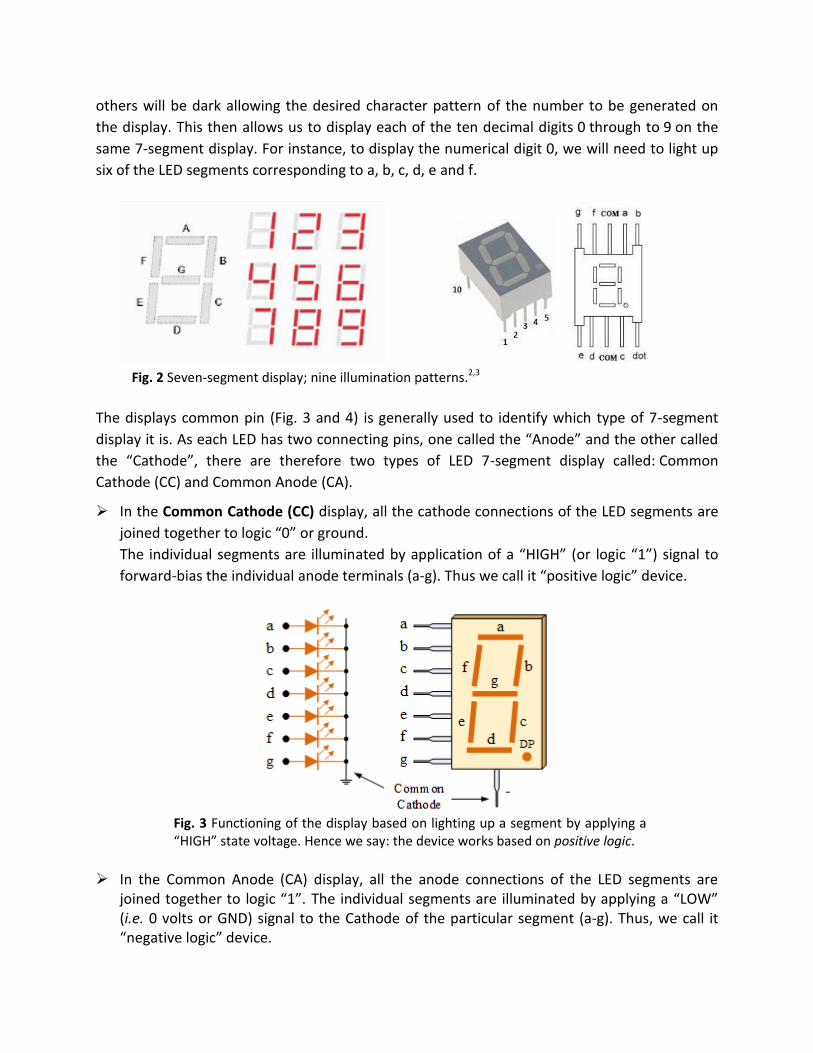
others will be dark allowing the desired character pattern of the number to be generated on
the display. This then allows us to display each of the ten decimal digits 0 through to 9 on the
same 7-segment display. For instance, to display the numerical digit 0, we will need to light up
six of the LED segments corresponding to a, b, c, d, e and f.
Fig. 2 Seven-segment display; nine illumination patterns.2,3
The displays common pin (Fig. 3 and 4) is generally used to identify which type of 7-segment
display it is. As each LED has two connecting pins, one called the “Anode” and the other called
the “Cathode”, there are therefore two types of LED 7-segment display called: Common
Cathode (CC) and Common Anode (CA).
In the Common Cathode (CC) display, all the cathode connections of the LED segments are
joined together to logic “0” or ground.
The individual segments are illuminated by application of a “HIGH” (or logic “1”) signal to
forward-bias the individual anode terminals (a-g). Thus we call it “positive logic” device.
Fig. 3 Functioning of the display based on lighting up a segment by applying a “HIGH” state voltage. Hence we say: the device works based on positive logic.
In the Common Anode (CA) display, all the anode connections of the LED segments are
joined together to logic “1”. The individual segments are illuminated by applying a “LOW” (i.e. 0 volts or GND) signal to the Cathode of the particular segment (a-g). Thus, we call it “negative logic” device.

Fig 4. Functioning of the display based on lighting up a segment by applying a “LOW” state voltage. Hence we say, the device works based on “negative logic”.
In general, common anode displays are more popular as many logic circuits can sink more current than they can source.
3. Numerical Basis [Taken from Ref4] 3.1 Decimal numbers (base 10)
Decimal numbers have 10 different digits to be represented (0, 1, 2, 3, 4, 5, 6, 7, 8, 9).
3.2 Hexadecimal numbers (base 16)
Hexadecimal numbers have 16 different digits to be represented (0, 1, 2, 3, 4, 5, 6, 7, 8,
9, and the letters A, B, C, D, E and F).
Hexadecimal (C) Decimal Binary
0 0 0
0x1 1 (one) 0 1
0x2 2 (two) 1 0
0x3 3 (three) 1 1
0x4 4 (four) 1 0 0
0x5 5 (five) 1 0 1

0x6 6 (six) 1 1 0
0x7 7 (seven) 1 1 1
0x8 8 (eight) 1 0 0 0
0x9 9 (nine) 1 0 0 1
0xA 10 (ten) 1 0 1 0
0xB 11 (eleven) 1 0 1 1
0xC 12 (twelve) 1 1 0 0
0xD 13 (thirteen) 1 1 0 1
0xE 14 (fourteen) 1 1 1 0
0xF 15 (fifteen) 1 1 1 1
0x10 16 (sixteen) 1 0 0 0 0
0x11 17 (seventeen) 1 0 0 0 1
… …
In C++, hexadecimal numbers are preceded by 0x (zero, x).
One way to translate a number from a base to another is the following:
3.3 Binary representations
Octal and hexadecimal numbers have a considerable advantage over our decimal
numbers in the world of bits. It is that their bases (8 and 16) are perfect multiples of 2
(23 and 24, respectively), which allows us to make easier conversions from these bases
to binary than from decimal numbers (whose base is 2x5).
For example, suppose that we want to translate the following binary sequence to
numbers of other bases:
110011111010010100 (number in base 2)
In order to translate it to decimal we would need to conduct a mathematical
operation similar to the one we have used previously 1x 217 + 1x 216 + 0x 215+ …, which
would give us the decimal number 212628.

To pass this sequence to octal we proceed as follows: Since 8 is 23, we will separate
the binary value in groups of 3 numbers:
110 011 111 010 010 100
and now we just have to translate to octal base each group separately:
110 011 111 010 010 100 (base 2)
6 3 7 2 2 4 (base 8)
giving the number 637224 as result.
This same process can be inversely performed to pass from octal to binary.
To pass this sequence to hexadecimal numbers we perform the same process but
separating the binary value in groups of 4 numbers, because 16 is 24:
11 0011 1110 1001 0100 (base 2) 3 3 E 9 4 (base 16)
Therefore, the binary expression 110011111010010100 can be represented in C++ either as 212628 (decimal), as 0637224 (octal) or as 0x33e94 (hexadecimal). The hexadecimal code is especially interesting since nowadays, computers are compatible with bytes composed of 8 binary bits and therefore each byte matches with the range that 2 hexadecimal numbers can represent. For that reason it is so frequently used to represent values translated to or from binary base.
4. Experimental tasks
In every project we identify three distinct sections
which will be used as a reference when describing the 7-segment display application.
4.1 To design a combinational logic circuit to display characters from 0 to 9 in a 7-segment display
Step-1 Construct a truth table, which should indicate the individual segments that need to be illuminated in order to produce the required decimal digit from 0 through 9 (i.e. establish the 7-segment binary coding).
Step-2 Express the binary coding into hexadecimal coding. It will be a good practice to do this step on your own.
Assignment: Check if the truth table suggested in Fig. 5 is correct.

Fig 5. Illustration of a 7- segment display and the suggested truth table. The truth table constitutes the Mathematical Model for the display. You have to verify if the whole table is correct.
The table in Fig.5 above constitutes our decoder. We now know which pins have to be
connected to a HIGH level in order to display the desired digit.
In past versions of this lab, we used NAND and NOR electronic gates to, for a given binary input,
establish the proper logical levels (HIGH or LOW) at the pins of the 7-segment display. This time,
we will use instead the ARDUINO to implement that process. That is, we will be “interfacing the
7-segment display with the Arduino microcontroller.”
Step-2 Connect the abcdefg pins to the digital ports
D4-D10 of the microcontroller (Fig.5).
Connect the COM with a 1Kresistor to GND.
Remember we are using a positive logic de-
vice(i.e. LEDs light up when a HIGH level signal is placed at the corresponding anode).

Fig 6. Connection of the arduino board to a 7-seg display.
Step-3 Load the following program into your microcontroller board.
// This program contains global variables, array, etc.
/ / I. Here we implement the math model.
(interaction between the code and the math model)
const char disp[]={0x3f, 0x06, 0x5b, 0x4f, 0x66, 0x6d, 0x7d,
0x07, 0x7f, 0x6f, 0x77, 0x7c, 0x39, 0x5e, 0x79, 0x71, 0x80 };
// This is to define the library; i.e putting in the
// array disp the information given in Fig.5
// II. This section is for interfacing the hardware-section with the code-section.
void setup() {
// put your setup code here, to run once:
for (int i=4; i<=11; i++) // the increase operator (++) increase by one the value // stored in a variable. // i++; // is equivalent to // i = i+1; // Below in the program we will make j=4 pinMode( i, OUTPUT);
}
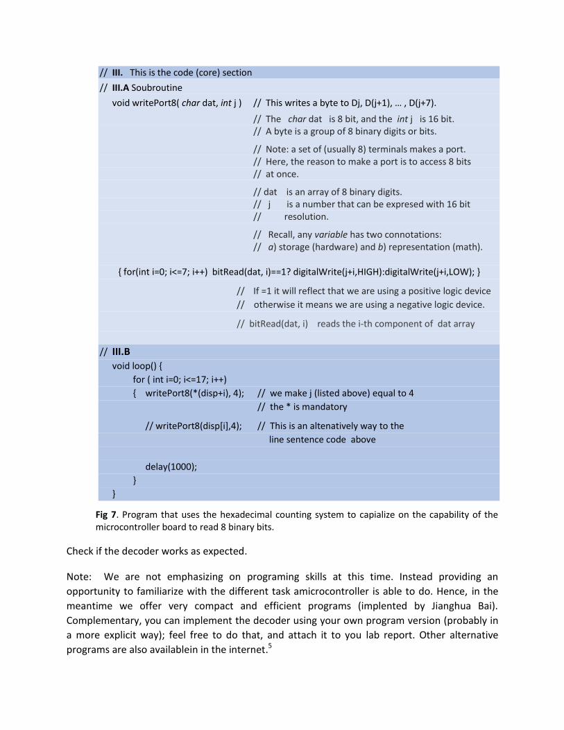
// III. This is the code (core) section
// III.A Soubroutine
void writePort8( char dat, int j ) // This writes a byte to Dj, D(j+1), … , D(j+7).
// The char dat is 8 bit, and the int j is 16 bit. // A byte is a group of 8 binary digits or bits.
// Note: a set of (usually 8) terminals makes a port. // Here, the reason to make a port is to access 8 bits // at once.
// dat is an array of 8 binary digits. // j is a number that can be expresed with 16 bit // resolution.
// Recall, any variable has two connotations: // a) storage (hardware) and b) representation (math). { for(int i=0; i<=7; i++) bitRead(dat, i)==1? digitalWrite(j+i,HIGH):digitalWrite(j+i,LOW); }
// If =1 it will reflect that we are using a positive logic device
// otherwise it means we are using a negative logic device.
// bitRead(dat, i) reads the i-th component of dat array
// III.B
void loop() {
for ( int i=0; i<=17; i++)
{ writePort8(*(disp+i), 4); // we make j (listed above) equal to 4
// the * is mandatory
// writePort8(disp[i],4); // This is an altenatively way to the
line sentence code above
delay(1000);
}
}
Fig 7. Program that uses the hexadecimal counting system to capialize on the capability of the microcontroller board to read 8 binary bits.
Check if the decoder works as expected.
Note: We are not emphasizing on programing skills at this time. Instead providing an
opportunity to familiarize with the different task amicrocontroller is able to do. Hence, in the
meantime we offer very compact and efficient programs (implented by Jianghua Bai).
Complementary, you can implement the decoder using your own program version (probably in
a more explicit way); feel free to do that, and attach it to you lab report. Other alternative
programs are also availablein in the internet.5

Step-4 Standalone microcontroller. After you finish the sections above, unplug the USB cable
between your Arduino board and your computer. Use a different power supply to power
the Arduino board and watch what happens. The purpose of this step is to show that
the Arduino is an actual computer. After we program them, they can run by themselves.
That is one reason why microcontrollers are very popular. After they are programmed,
they can be powered by batteries and be used to control portable appliances.
4.2 Controlling the brightness of the 7-seg display with Pulse Width Modulation (PWM)
How to achieve analog control with a digital controller? Pulse width modulation is an easy
way. Suppose one sets the output of a terminal with a TTL logic signal. If one outputs HIGH
during 50% of the time and LOW during the other 50% of the time (i.e. 50% duty cycle), the
average effect at the terminal will somewhat equivalent to keeping 2.5V all the time. If one sets
HIGH 80% and LOW 20% of the time (i.e. 80% duty cycle), the average output at the terminal
will be as if one is applying 4V all the time. That is, one changes the duty cycle of the digital
pulses in order to produce an average analog effect at the port; this is called PWM. (But
remember the PWM output at a port is not a digital-to-analog converter).
Now, repeat section 4.1, but remove the 300 ohms resistor between COM and GND.
Connect the COM to D2 directly. Modify the loop() function with the block shown below.
Change the delay time, and check what happens. Monitor the COM with an oscilloscope.
Fig 8. Illustration of puses of different duty cycle used in PWM.
void loop() {
for (int i=0; i<=17; i++)

{ writePort8(*(disp+i),4);
For( int j=0; j<80;j++) // This FOR is for implementing PWM
// see comment below, beneath the program
{ digitalWrite(2, LOW), delayMicroseconds(1);
digitalWrite(2,HIGH),delayMicroseconds(20); // change here, from 20—1,
// and check the brightness.
// Notice we are implementing PWM through pin#2
}
}
}
Fig 9.
The PWM here we are using is negative logic. Why? Because our display is positive logic, common cathode, through which the LEDs are connected to GND. Now we connect the common cathode to our PWM pin. The PWM pin serves as the GND. So, the PWM here is negative logic.
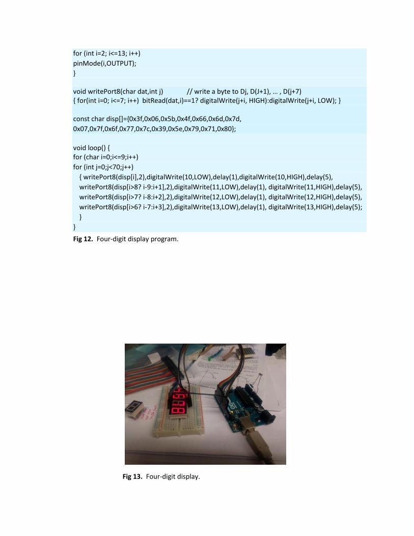
4.3 Four-digit display (Hardware of the device: The four digits share the same data bus, and thus share the
same data information) With the capability to activate only one ”7-segment display” at a time, we plan to operate up to
four ”7-segment display” in such a way that the user observes the counting of up to 4 digit numbers.
The trick here is that, even though we light up ONE digit at a time, we can light up (sequentially) more
than one but so fast that the human perception will not notice it. First digit ONE is lighted up and the
other 3 are kept off; then we light up digit TWO and other 3 are kept off.; and so on. A given four-digit
number remains displayed until an activation signal is given to the device.
Step-1 Connect A-F to Arduino D2—D8. Connect display D1-D4 to Arduino D10---D13.
All the corresponding abcdefg LED of the four displays are correspondingly connected
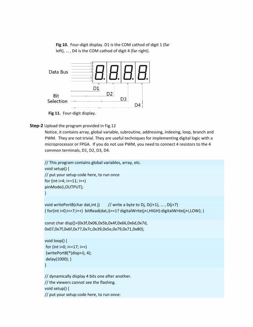
Fig 10. Four-digit display. D1 is the COM cathod of digit 1 (far
left), … , D4 is the COM cathod of digit 4 (far right).
Fig 11. Four-digit display.
Step-2 Upload the program provided in Fig.12
Notice, it contains array, global variable, subroutine, addressing, indexing, loop, branch and
PWM. They are not trivial. They are useful techniques for implementing digital logic with a
microprocessor or FPGA. If you do not use PWM, you need to connect 4 resistors to the 4
common terminals, D1, D2, D3, D4.
// This program contains global variables, array, etc.
void setup() {
// put your setup code here, to run once
for (int i=4; i<=11; i++)
pinMode(i,OUTPUT);
}
void writePort8(char dat,int j) // write a byte to Dj, D(J+1), … , D(j+7)
{ for(int i=0;i<=7;i++) bitRead(dat,i)==1? digitalWrite(j+i,HIGH):digitalWrite(j+i,LOW); }
const char disp[]={0x3f,0x06,0x5b,0x4f,0x66,0x6d,0x7d,
0x07,0x7f,0x6f,0x77,0x7c,0x39,0x5e,0x79,0x71,0x80};
void loop() {
for (int i=0; i<=17; i++)
{writePort8(*(disp+i), 4);
delay(1000); }
} // dynamically display 4 bits one after another.
// the viewers cannot see the flashing.
void setup() {
// put your setup code here, to run once:
for (int i=2; i<=13; i++)
pinMode(i,OUTPUT);
} void writePort8(char dat,int j) // write a byte to Dj, D(J+1), … , D(j+7) { for(int i=0; i<=7; i++) bitRead(dat,i)==1? digitalWrite(j+i, HIGH):digitalWrite(j+i, LOW); } const char disp[]={0x3f,0x06,0x5b,0x4f,0x66,0x6d,0x7d,
0x07,0x7f,0x6f,0x77,0x7c,0x39,0x5e,0x79,0x71,0x80};
void loop() { for (char i=0;i<=9;i++)
for (int j=0;j<70;j++)
{ writePort8(disp[i],2),digitalWrite(10,LOW),delay(1),digitalWrite(10,HIGH),delay(5),
writePort8(disp[i>8? i-9:i+1],2),digitalWrite(11,LOW),delay(1), digitalWrite(11,HIGH),delay(5),
writePort8(disp[i>7? i-8:i+2],2),digitalWrite(12,LOW),delay(1), digitalWrite(12,HIGH),delay(5),
writePort8(disp[i>6? i-7:i+3],2),digitalWrite(13,LOW),delay(1), digitalWrite(13,HIGH),delay(5);
}
}
Fig 12. Four-digit display program.
Fig 13. Four-digit display.

4.4 Four-digit display integrated with a counter
In lab 2, the counter design uses the computer monitor as your display. Here we use the 4 digit LED
instead as your displayer. For that purpose let’s rebuild the counter. One has to tune the analog
threshold properly and the LED displayer in order to make the whole project work.
// This program demonstrate a digital flip-flop and a digital counter!
void setup() {
pinMode(A0,INPUT);
for (int i=2;i<=13;i++)
pinMode(i,OUTPUT);
}
// dynamically display 4 bits one after another.
// the viewers cannot see the flashing.
void writePort8(char dat,int j) // write a byte to Dj, D(j+1), … , D(j+7), 8 bits together!
{ for(int i=0;i<=7;i++) bitRead(dat,i)==1? digitalWrite(j+i,HIGH):digitalWrite(j+i,LOW); }
const char disp[]={0x3f,0x06,0x5b,0x4f,0x66,0x6d,0x7d,
0x07,0x7f,0x6f,0x77,0x7c,0x39,0x5e,0x79,0x71,0x80};
void write4digits(int dat)
{
int i4=dat%10;
int i3=dat%100/10;
int i2=dat%1000/100;
int i1=dat/1000;
for (int j=0;j<30;j++)
{ writePort8(disp[i1],2),digitalWrite(10,LOW),delay(1),digitalWrite(10,HIGH),delay(5),
writePort8(disp[i2],2),digitalWrite(11,LOW),delay(1), digitalWrite(11,HIGH),delay(5),
writePort8(disp[i3],2),digitalWrite(12,LOW),delay(1), digitalWrite(12,HIGH),delay(5),
writePort8(disp[i4],2),digitalWrite(13,LOW),delay(1), digitalWrite(13,HIGH),delay(5);
// delay(8);
}
}
int s=0;
void loop() {
int j;
j=analogRead(A0);
if (j<349) // change this number according to your measurement.

{delay(3);
if (analogRead(A0)>350)
write4digits(++s);
}
}
Fig 14. Counter with LED display program.
Fig. 15. Counter with LED display.
Fig 14 Picture of the counter and display setup.
4.4 The dot matrix display
In the sections above, we first implemented a one-digit display (8 LEDs), and then a 4-digit
display (32 LEDs). Now we plan to use an 8-line x 8-column (64 LEDs) device as a display. This is the
dot matrix display.
In a dot matrix display, multiple LEDs are wired together in rows and columns. 6 This is done
to minimize the number of pins required to drive them. For example, a 8×8 matrix of LEDs
(shown in Fig. 15) would need 64 I/O pins, one for each LED pixel. By wiring all the anodes
together in rows (R1 through R8), and cathodes in columns (C1 through C8), the required
number of I/O pins is reduced to 16. Each LED is addressed by its row and column number. For
example, if R4 is pulled HIGH and C3 is pulled LOW, the LED in fourth row and third column will
be turned on. Characters can be displayed by fast scanning of either rows or columns, as
outlined below.

Figure 15. Structure of an 8x8 LED dot matrix.
Example
In this experiment we use a 8x8 LED dot matrix. The example provided below (Fig. 16 and 17)6
corresponds to a LED matrix of size 5×7, but the working principle is the same in a 8x8 dot
matrix.
Figure 16 shows which LEDs have to be turned on to display the English alphabet ‘A’.
The 7 rows and 5 columns are controlled through the microcontroller pins. Let’s see in detail
how it works.
Figure 16. A 5x7 LED dot matrix display.

Suppose, we want to display the letter ”A”.
We will first select the column C1, i.e. C1 is pulled LOW, and
deselect other columns by blocking their ground paths (i. e. C2 through C5 pins are pulled to
logic HIGH).
Now that the first column is active, and you need to turn on the LEDs in the rows R2 through
R7 of this column, which can be done by applying forward bias voltages to these rows.
Next, select the column C2 (and deselect all other columns), and apply forward bias to R1
and R5,
and so on.
Therefore, by scanning across the column quickly (> 100 times per second), and turning on the
respective LEDs in each row of that column, the persistence of vision comes in to play, and we
perceive the display image as still.
Figure 17. Scanning across the columns; at each column feeding the appropriate row values.6
Procedure
This experiment requires a lot combinational logic work. First, mapping the columns and
rows of the dot display with the characters intended to be displayed. Second, mapping the
hardware pinout of the dot-display to an orderly array so that the programing task can be made
simpler. Third, mapping the Arduino digital out with the display pinouts. Schematically, we
have to implement a composed mapping: C ( F ( D (16) ) ) , where D is Arduino digital port
mapping function. F is the display mapping function. C is the character mapping function.
Step-1. Connect pins 9 to 16 of the display with terminal D4 to D13 of the Arduino. Putting
the wires in color order, will save a lot of efforts.
Connect pins 1 to 6 of the display with terminals A0 to A5 of the Arduino.
Connect pins 7 of the display with terminal D3 of the Arduino.
Connect pins 8 of the display with terminal D2 of the Arduino.
The Arduino has limited digital terminals, so we have to use some of the analog
terminals as our digital terminals. See the table shown below.
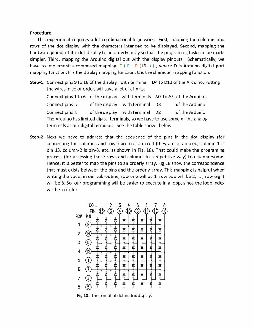
Step-2. Next we have to address that the sequence of the pins in the dot display (for
connecting the columns and rows) are not ordered (they are scrambled; column-1 is
pin 13, column-2 is pin-3, etc. as shown in Fig. 18). That could make the programing
process (for accessing those rows and columns in a repetitive way) too cumbersome.
Hence, it is better to map the pins to an orderly array. Fig 18 show the correspondence
that must exists between the pins and the orderly array. This mapping is helpful when
writing the code; in our subroutine, row one will be 1, row two will be 2, … , row eight
will be 8. So, our programming will be easier to execute in a loop, since the loop index
will be in order.
Fig 18. The pinout of dot matrix display.
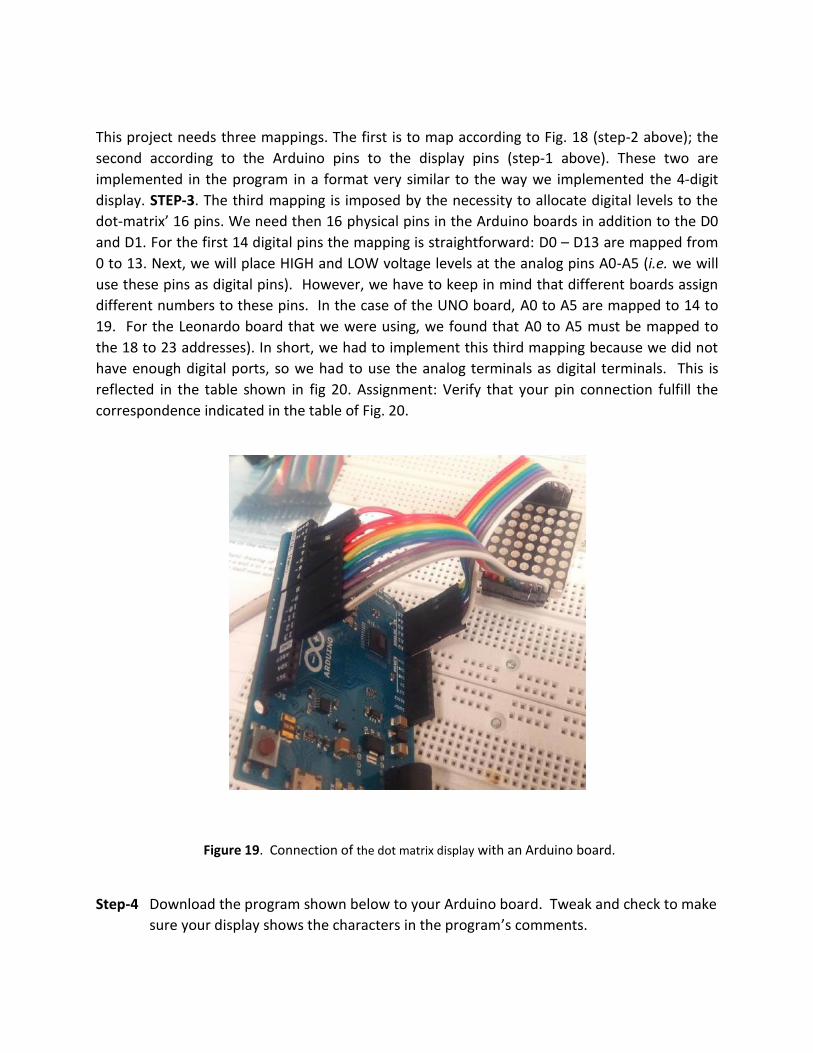
This project needs three mappings. The first is to map according to Fig. 18 (step-2 above); the
second according to the Arduino pins to the display pins (step-1 above). These two are
implemented in the program in a format very similar to the way we implemented the 4-digit
display. STEP-3. The third mapping is imposed by the necessity to allocate digital levels to the
dot-matrix’ 16 pins. We need then 16 physical pins in the Arduino boards in addition to the D0
and D1. For the first 14 digital pins the mapping is straightforward: D0 – D13 are mapped from
0 to 13. Next, we will place HIGH and LOW voltage levels at the analog pins A0-A5 (i.e. we will
use these pins as digital pins). However, we have to keep in mind that different boards assign
different numbers to these pins. In the case of the UNO board, A0 to A5 are mapped to 14 to
19. For the Leonardo board that we were using, we found that A0 to A5 must be mapped to
the 18 to 23 addresses). In short, we had to implement this third mapping because we did not
have enough digital ports, so we had to use the analog terminals as digital terminals. This is
reflected in the table shown in fig 20. Assignment: Verify that your pin connection fulfill the
correspondence indicated in the table of Fig. 20.
Figure 19. Connection of the dot matrix display with an Arduino board.
Step-4 Download the program shown below to your Arduino board. Tweak and check to make
sure your display shows the characters in the program’s comments.
The microcontroller can process 8 bits at a time. So, one can either light up 8 LEDs in a column
or 8 LEDs in a row at a time. Then light other columns or rows. We can also process pixel by
pixel. This way, we are playing with 64 elements. Surely we can display more effects, but the
programming will be more sophisticated.
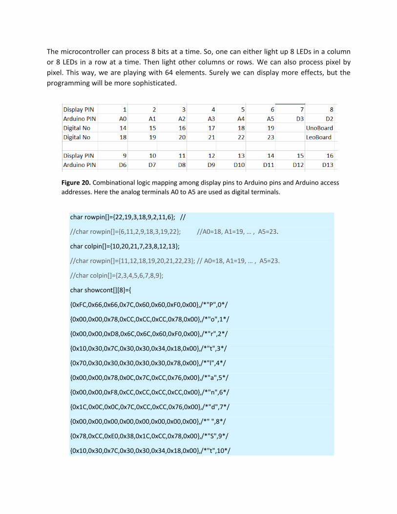
Figure 20. Combinational logic mapping among display pins to Arduino pins and Arduino access
addresses. Here the analog terminals A0 to A5 are used as digital terminals.
char rowpin[]={22,19,3,18,9,2,11,6}; //
//char rowpin[]={6,11,2,9,18,3,19,22}; //A0=18, A1=19, … , A5=23.
char colpin[]={10,20,21,7,23,8,12,13};
//char rowpin[]={11,12,18,19,20,21,22,23}; // A0=18, A1=19, … , A5=23.
//char colpin[]={2,3,4,5,6,7,8,9};
char showcont[][8]={
{0xFC,0x66,0x66,0x7C,0x60,0x60,0xF0,0x00},/*"P",0*/
{0x00,0x00,0x78,0xCC,0xCC,0xCC,0x78,0x00},/*"o",1*/
{0x00,0x00,0xD8,0x6C,0x6C,0x60,0xF0,0x00},/*"r",2*/
{0x10,0x30,0x7C,0x30,0x30,0x34,0x18,0x00},/*"t",3*/
{0x70,0x30,0x30,0x30,0x30,0x30,0x78,0x00},/*"l",4*/
{0x00,0x00,0x78,0x0C,0x7C,0xCC,0x76,0x00},/*"a",5*/
{0x00,0x00,0xF8,0xCC,0xCC,0xCC,0xCC,0x00},/*"n",6*/
{0x1C,0x0C,0x0C,0x7C,0xCC,0xCC,0x76,0x00},/*"d",7*/
{0x00,0x00,0x00,0x00,0x00,0x00,0x00,0x00},/*" ",8*/
{0x78,0xCC,0xE0,0x38,0x1C,0xCC,0x78,0x00},/*"S",9*/
{0x10,0x30,0x7C,0x30,0x30,0x34,0x18,0x00},/*"t",10*/

{0x00,0x00,0x78,0x0C,0x7C,0xCC,0x76,0x00},/*"a",11*/
{0x10,0x30,0x7C,0x30,0x30,0x34,0x18,0x00},/*"t",12*/
{0x00,0x00,0x78,0xCC,0xFC,0xC0,0x78,0x00},/*"e",13*/
{0x00,0x00,0x00,0x00,0x00,0x00,0x00,0x00},/*" ",14*/
{0xCC,0xCC,0xCC,0xCC,0xCC,0xCC,0xFC,0x00},/*"U",15*/
{0x00,0x00,0xF8,0xCC,0xCC,0xCC,0xCC,0x00},/*"n",16*/
{0x30,0x00,0x70,0x30,0x30,0x30,0x78,0x00},/*"i",17*/
{0x00,0x00,0xCC,0xCC,0xCC,0x78,0x30,0x00},/*"v",18*/
{0x00,0x00,0x78,0xCC,0xFC,0xC0,0x78,0x00},/*"e",19*/
{0x00,0x00,0xD8,0x6C,0x6C,0x60,0xF0,0x00},/*"r",20*/
{0x00,0x00,0x7C,0xC0,0x78,0x0C,0xF8,0x00},/*"s",21*/
{0x30,0x00,0x70,0x30,0x30,0x30,0x78,0x00},/*"i",22*/
{0x10,0x30,0x7C,0x30,0x30,0x34,0x18,0x00},/*"t",23*/
{0x00,0x00,0xCC,0xCC,0xCC,0x7C,0x0C,0xF8},/*"y",24*/
{0x00,0x00,0x00,0x00,0x00,0x70,0x30,0x60},/*",",25*/
{0x00,0x00,0x00,0x00,0x00,0x00,0x00,0x00},/*" ",26*/
{0xFC,0x66,0x66,0x7C,0x60,0x60,0xF0,0x00},/*"P",27*/
{0xE0,0x60,0x6C,0x76,0x66,0x66,0xE6,0x00},/*"h",28*/
{0x00,0x00,0xCC,0xCC,0xCC,0x7C,0x0C,0xF8},/*"y",29*/
{0x00,0x00,0x7C,0xC0,0x78,0x0C,0xF8,0x00},/*"s",30*/
{0x30,0x00,0x70,0x30,0x30,0x30,0x78,0x00},/*"i",31*/
{0x00,0x00,0x78,0xCC,0xC0,0xCC,0x78,0x00},/*"c",32*/
{0x00,0x00,0x7C,0xC0,0x78,0x0C,0xF8,0x00},/*"s",33*/
{0x00,0x00,0x00,0x00,0x00,0x00,0x00,0x00},/*" ",34*/
{0xFC,0x6C,0x66,0x66,0x66,0x6C,0xFC,0x00},/*"D",35*/
{0x00,0x00,0x78,0xCC,0xFC,0xC0,0x78,0x00},/*"e",36*/
{0x00,0x00,0xDC,0x66,0x66,0x7C,0x60,0xF0},/*"p",37*/
{0x10,0x30,0x7C,0x30,0x30,0x34,0x18,0x00},/*"t",38*/
{0x00,0x00,0x00,0x00,0x00,0x70,0x30,0x60},/*",",39*/

{0x00,0x00,0x00,0x00,0x00,0x00,0x00,0x00},/*" ",40*/
{0xFC,0x66,0x66,0x7C,0x60,0x60,0xF0,0x00},/*"P",41*/
{0xCC,0xCC,0xCC,0xFC,0xCC,0xCC,0xCC,0x00},/*"H",42*/
{0x78,0xCC,0x0C,0x38,0x0C,0xCC,0x78,0x00},/*"3",43*/
{0x30,0xF0,0x30,0x30,0x30,0x30,0xFC,0x00},/*"1",44*/
{0xFC,0xC0,0xF8,0x0C,0x0C,0xCC,0x78,0x00},/*"5",45*/
};
void setup()
{
for (char i=2;i<=9;i++) pinMode(i,OUTPUT),digitalWrite(i,HIGH);
for (char i=11;i<=23;i++) pinMode(i,OUTPUT),digitalWrite(i,LOW);
}
void loop() {
for (char k=0;k<=45;k++)
{
for(int m=0;m<300;m++)
{for (char i=0;i<=7;i++)
{ digitalWrite(rowpin[i],HIGH); // light one row
for(char j=0;j<=7;j++) // light column one after another.
{ digitalWrite(colpin[j],bitRead(showcont[k][i],j)==1? LOW:HIGH); //show the words.
delayMicroseconds(1); // ON one column.
digitalWrite(colpin[j],HIGH); // OFF one column.
delayMicroseconds(1); //PWM to dim the LEDs.
}
digitalWrite(rowpin[i],LOW); // OFF one row.
}
}
delay(500);
}
}
Fig 21. Dot matrix program.
Assignments:
Verify that the hex coding in the program above reflects the intended character. Hint: Do it from the
hexadecimal to the character shape.

Modify the program to display your name (show it the instructor when done).
1 http://www.binaryhexconverter.com/binary-to-hex-converter Binary is the simplest kind of number system that uses only two digits of 0 and 1. By using these digits
computational problems can be solved by machines because in digital electronics a transistor is used in two states. Those two states can be represented by 0 and 1. That is why this number system is the most preferred in modern computer engineer, networking and communication specialists, and other professionals.
Hex, or hexadecimal, is a number system of base 16. This number system is especially interesting because in our casually used decimal system we have only 10 digits to represent numbers. As hex system has 16 digits, the extra needed 6 digits are represented by the first 6 letters of English alphabet. Hence, hex digits are 0,1,2,3,4,5,6,7,8 and 9 A, B, C, D, E, F. This number system is the most commonly used in mathematics and information technologies.
Binary to hex conversion examples (1110)2 = 0E (111001)2 = 39 (10011100)2 = 9C
Binary to Hexadecimal Conversion Chart
Binary Hexadecimal
0000 0
0001 1
0010 2
0011 3
0100 4
0101 5
0110 6
0111 7
1000 8
1001 9
1010 A
1011 B
1100 C
1101 D
1110 E
1111 F
2 http://www.realdigital.org/document/28
3 http://www.engineersgarage.com/tutorials/seven-segment-testing
4 http://www.cplusplus.com/doc/hex/
5 http://circuitdigest.com/microcontroller-projects/7-segment-display-interfacing-with-arduino
6 http://embedded-lab.com/blog/lab-12-basics-of-led-dot-matrix-display/