1 Introduction to Microcontroller Microcontroller Fundamentals & Programming.

Microcontrollerbased peak current mode control using digital slope compensation Article
Accepted Version
Hallworth, M. and Shirsavar, A. (2012) Microcontrollerbased peak current mode control using digital slope compensation. IEEE Transactions on Power Electronics, 27 (7). pp. 33403351. ISSN 08858993 doi: https://doi.org/10.1109/TPEL.2011.2182210 Available at http://centaur.reading.ac.uk/31751/
It is advisable to refer to the publisher’s version if you intend to cite from the work.
To link to this article DOI: http://dx.doi.org/10.1109/TPEL.2011.2182210
Publisher: IEEE
All outputs in CentAUR are protected by Intellectual Property Rights law, including copyright law. Copyright and IPR is retained by the creators or other copyright holders. Terms and conditions for use of this material are defined in the End User Agreement .
www.reading.ac.uk/centaur
CentAUR

Central Archive at the University of Reading
Reading’s research outputs online

1
Microcontroller Based Peak Current Mode
Control Using Digital Slope CompensationMichael Hallworth, Member, IEEE, and Seyed Ali Shirsavar.
Abstract
Microcontroller based peak current mode control of a Buck converter is investigated. The new solution uses a
discrete time controller with digital slope compensation. This is implemented using only a single-chip microcontroller
to achieve desirable cycle-by-cycle peak current limiting. The digital controller is implemented as a two pole, two
zero linear difference equation designed using a continuous time model of the Buck converter and a discrete time
transform. Subharmonic oscillations are removed with digital slope compensation using a discrete staircase ramp. A
16W hardware implementation directly compares analog and digital control. Frequency response measurements are
taken and it is shown that the crossover frequency and expected phase margin of the digital control system match
that of its analog counterpart.
Index Terms
Digital peak current mode control, DC-DC switch mode power supplies, discrete controller, digital slope com-
pensation.
Both authors are with the School of Systems Engineering, The University of Reading, England. Corresponding author: Michael Hallworth.
E-mail: [email protected]. Postal: School of Systems Engineering, University of Reading, Whiteknights, Reading, Berkshire,
RG6 6AY, England. Phone: +44(0)7891 353 129. Fax: +44(0)1189 751 994. This paper has been submitted solely to IEEE Transactions on
Power Electronics and has not been presented at a conference.

2
NOMENCLATURE
CO Output filter capacitor.
D Duty ratio.
IO Output current.
LO Output filter inductor.
QC Double pole quality factor.
Ramp Digital ramp height.
Steps Number of digital steps per slope compensation period.
SE External ramp slope.
SN Output inductor current slope.
TS Switching period.
TSLOPE Digital slope compensation period.
TSTEP Time taken to decrement digital ramp.
VDAC DAC voltage range.
VIN Input voltage.
VO Output voltage.
VPP Compensation ramp height.
mC Slope compensation factor.
n Turns ratio, n = NS/NP .
nDAC Number of DAC bits.
ΔRamp Change in digital ramp height per step.
ΦE Phase erosion.
ΦM Required open-loop phase margin.
ωCP0 Compensator pole at origin.
ωCP1 Compensator pole.
ωCZ1 Compensator zero.
ωN Plant double pole.
ωP1 Plant pole.
ωP1 Plant zero.
ωX Required open-loop crossover frequency.
I. INTRODUCTION
II. REVIEW OF PEAK CURRENT MODE CONTROL
Figure 1 depicts the typical set up for analog peak current mode control of a Buck converter. The output voltage
along with a reference voltage are used as inputs to an error amplifier. The capacitors and resistors in the feedback

3
SlopeCompensation
Comparator
Error Amp
PWM
RILO
CO RO
VO
PWM
VS
C3
C1 R2
R1
RbVREF
Fig. 1. Analog peak current mode control of a Buck converter.
Comparator PWM
RILO
CO RO
VO
PWM
VS
R1
Rb
DAC ADC2p2zController
Digital SlopeCompensation
Mixed SignalMicrocontroller Digital Control
Fig. 2. Digital peak current mode control of a Buck converter.
path of the error amplifier form the poles and zeros of the compensation network. The output of the error amplifier
forms the current reference voltage before slope compensation.
The peak of the output inductor current is sensed by measuring the current through the switch using either a
small current sense resistor or a current transformer; both of which have an equivalent current-to-voltage gain of RI .
The sensed current is effectively a ramp; as the switch is turned on at the beginning of the pulse width modulation
(PWM) period the current through it increases from its minimum to the maximum by the end of the duty period.
This sensed current is used as an input to a comparator. The second input to the comparator is the control
voltage obtained from the error amplifier and compensation network. This forms the inner control loop; the current
loop. Compensators can be designed for both outer and inner control loops [1], however only the outer loop is
compensated in peak current mode.
When the sensed current reaches the value of the control voltage the output of the comparator changes and this
4
is used to trigger the end of the PWM duty cycle. Effectively the current through the inductor is limited and the
plant acts as a constant current source. However, due to the voltage feedback, the converter is also able to regulate
a constant voltage across a varying load.
For the digital implementation of peak current mode control presented in this paper, all of the analog control
components are replaced by a single microcontroller as shown in Figure 2. Initially the PWM duty cycle is set
to 100% and current is conducted through the switch. The output voltage is applied, through a sampling divider,
to the ADC of the microcontroller. The analog voltage is sampled and converted to a digital value. This digital
representation of the output voltage has a reference voltage (another digital value) subtracted from it and the resulting
discrete time error signal is used as an input to a discrete time controller.
The capacitors and resistors of the analog compensation network are replaced by the digital coefficients of the
controller. The controller design will be discussed in detail in Section VI. The output of the controller, a number, is
scaled appropriately and used as an input to the microcontroller’s digital-to-analog (DAC) module. This generates
the current reference voltage.
The switch current is sensed using the same method as with analog control. The sensed current is used as the
other input to the microcontroller’s on-board comparator module with the first input supplied directly from the
output of the DAC module. When the sensed current ramp reaches the control voltage the comparator’s output will
change. This is used as a trip inside the microcontroller to reset the PWM output and disable the switch. The result
is the same operation of peak current mode control so commonly implemented in analog. Slope compensation is
still required with the analog controller and this must also be implemented in digital. This will be discussed in the
next Section.
III. CURRENT LOOP AND SLOPE COMPENSATION
An analysis of peak current mode control by Ridley in [2] determined that the subharmonic oscillations observed
during peak current mode control could be represented by a double pole at half the switching frequency, FS .
ωN = πFS (1)
The subharmonic oscillations can be removed by ensuring that the resonant peak of this double pole is sufficiently
damped. The peak should be damped such that it does not cross the unity gain axis of the open loop system. This
can be achieved by setting the quality factor, QC , of the double pole to QC ≤ 1. Using this, the slope compensation
factor, mC , can be calculated. The slope compensation factor specifies the ratio of external compensation slope to
output inductor slope required in order to sufficiently damp the subharmonic oscillations.
mC =1 + π
2 .QC
π.QC . (1−D)(2)
Where D is the duty cycle calculated in 3.
5
D =VO + VDIODE
VIN(3)
Using the slope compensation factor calculated in 2, the external ramp slope, SE , can be found using the output
inductor slope, SN . For Buck derived topologies, the output inductor current slope during the time that the switch
is on is calculated in 4.
SN =(n.VIN )− VOUT − VDIODE
LO.RI .n (4)
SE = (mC − 1) .SN (5)
Thus, the quality factor of the resonant peak at half the switching frequency determines the compensation ramp
requirements. The required peak-to-peak value of the compensation ramp is calculated using 6.
VPP = SE .TS (6)
There is no transformer with a Buck converter and so in the above equations n = NS/NP = 1. However these
equations are valid for other Buck derived topologies which include transformers; such as half or full-bridge. If a
transformer is used there will be a certain amount of slope compensation provided by the magnetizing inductance
of the transformer [3].
IV. COMPENSATOR DESIGN
Using the simplified model of a PWM switch [4], an accurate model for the small-signal characteristics of peak
current mode control is presented in [2] with further information in [3]. Other models are available [5] and could be
investigated, however, the model in [2] is used as it performs well when compared to the hardware measurements.
The subharmonic oscillations observed with peak current mode control due to small perturbations in the inductor
current are predicted by this model. The compensation ramp discussed in the previous Section is added to the
sensed switch current to damp these oscillations.
Many implementations take an intuitive approach to compensator design. However this paper uses an exact
method to calculate the compensator poles and zeros such that the specified open loop crossover and phase margin
are achieved. Using the accurate control-to-output model proposed by Ridley in [2] a Type II compensator can be
analytically designed.
With peak current mode control the compensator is placed within the outer voltage loop. The inner current loop
has a bandwidth of between 1/6th and 2/3rds of the switching frequency [6], [7]. Therefore the crossover frequency
of the outer voltage loop should be less than this; between 1/20th and 1/10th of the switching frequency. The
transfer function of the Type II compensator, given in 7, has one pole, one zero and a pole at the origin.
6
HC (s) =ωCP0
s×
(1 + s
ωCZ1
)(1 + s
ωCP1
) (7)
The compensator pole, ωCP1, is placed at the frequency of the plant’s zero formed by the capacitor and its
parasitic ESR.
ωCP1 = ωESR =1
RESRCO(8)
Intuitive placement of the compensator zero is normally used to add phase in to the open loop system around the
crossover frequency. However, in this paper an exact equation is derived which analytically places the compensator
zero so as to achieve the phase margin specification precisely.
At the crossover frequency, the combined control-to-output and compensator transfer functions must satisfy 9.
Where φM is the required phase margin in radians and ωX is the required crossover frequency. HP (jω) and
HC (jω) are the control-to-output and controller transfer functions respectively.
∠ (HP (jωX)×HC (jωX)) = −π + φM (9)
Through knowledge of the control-to-output transfer function as given in [2], [3] and 7, an equation for calculating
the compensator zero is derived in this paper and given in 10 to precisely achieve a specified phase margin and
crossover frequency concurrently.
ωCZ1 =ωX
tan [φV ](10)
Where:
φV = −π
2+ φM + tan−1
(ωX
ωP1
)+ tan−1
(ωX
ωN1
)+ tan−1
(ωX
ωN2
)(11)
ωP1 =1
RO.CO+
TS
LO.CO. (mC . (1−D)− 0.5) (12)
ωN1 =−ωN
2.QC+
√1
Q2C .ω
2N
− 2 (13)
ωN2 =−ωN
2.QC−√
1
Q2C .ω
2N
− 2 (14)
In 11, the ωN1 and ωN2 terms are the complex conjugate poles of the high frequency double-pole ωN . The
inverse tangent of these pairs must be calculated accordingly. The phase contribution from ωCP1 negates that of
ωESR and as such these terms have been omitted from 11.

7
Finally, the gain of the compensator can be analytically calculated to achieve the specified crossover frequency of
the open loop system. This is the pole at the origin of the compensator and is the frequency at which this pole has
unity gain. However, the complete open loop system should have unity gain at the specified crossover frequency.
This is described in 15.
20 log10 [HP (jωX)] + 20 log10 [HC (jωX)] = 0 (15)
Using the control-to-output transfer function and 7, an equation for calculating the compensator pole at the origin
is given in 16 to achieve a specific crossover frequency.
ωCP0 =ωX
KDC ×K1 ×K2(16)
Where:
KDC =RO
n.RI× 1[
1 + RO.TS
LO. (mC . (1−D)− 0.5)
] (17)
K1 =
√1 +
(ω
ωCZ1
)2
√1 + ωX
ωP1
2(18)
K2 =1√(
1 + −ωX
ω2N
)2
+(
ωX
ωN .QC
)2(19)
V. DESIGN EXAMPLE
A 16W Buck converter is designed and constructed. An input voltage of 16V and output of 8V at 2A is used.
The full converter specification is given in Table Ia.
First, the slope compensation requirements are calculated given that the quality factor of the double pole at
half the switching frequency is set to 1. The remaining operational parameters are calculated using the converter
specification and equations presented in the previous Sections. Table Ib lists the parameters calculated for this
design example.
Using the exact analytical design method presented in this paper, the compensator is designed to meet the specified
phase margin and crossover frequency. For a Type II compensator, using 8, the pole is placed at the frequency of
the power stage ESR zero. 10 calculates the frequency of the compensator zero required to meet the phase margin
specification. Finally 16 calculates the gain of the compensator to meet the crossover specification.
The compensator poles and zeros are given in Table Ic. These exact values will be used in the next Section to
design the digital controller.
This design example is simulated using MATLAB. Figure 3 depicts the theoretical frequency response of the
control-to-output and controller transfer functions for the peak current mode converter design example. The controller

8
TABLE I
PEAK CURRENT MODE DESIGN EXAMPLE
Parameter Value Parameter Value
VIN 16V dc RI 0.48
VO 8V dc RESR 31mΩ
IO 2A VDIODE 0.6V
CO 440μF FS 200kHz
LO 22μH FX 15kHz
n 1 φM 75◦
(a) Specification
Parameter Value Parameter Value
QC 1 ωP1 732.6rad.s−1
D 0.5375 ωZ1 7.331× 10⁴rad.s−1
mC 1.7693 ωN 6.283× 10⁵rad.s−1
VPP 0.621V KDC 6.4631
(b) Operational parameters
Pole/Zero Value
ωCP1 7.331× 10⁴rad.s−1
ωCZ1 1.111× 10⁴rad.s−1
ωCP0 2.171× 10⁵rad.s−1
(c) Compensator poles and zeros
has been designed using the exact method presented in this paper. The plot of the combined open loop response is
stable as slope compensation is used and shows that the crossover frequency and phase margin, specified in Table
Ia, are achieved precisely in the open loop system.
VI. DIGITAL CONTROLLER DESIGN
Within one switching period the microcontroller must sample the analog output voltage, convert this to a digital
value, calculate the error, execute a controller based on this error and run the slope compensation algorithm using
the controller output to calculate the reference current. This is then compared to the sensed inductor current in
order to implement the peak current limit. When the sensed inductor current reaches the reference current a trip is
set within the microcontroller and the PWM duty is disabled.
In this digital implementation the controller has been designed in the continuous time domain and will be converted

9
101 102 103 104 105-50
0
50
Mag
nitu
de (d
B)
Frequency (Hz)
Control-to-OutputControllerOpen Loop
101 102 103 104 105-200
-150
-100
-50
0
Phas
e (D
egre
es)
Frequency (Hz)
Fig. 3. Theoretical frequency response plots of the control-to-output transfer, analytically designed controller and combined open loop. Open
loop crossover frequency: 15kHz, phase margin: 75◦.
to the discrete time domain using the bilinear transform. The bilinear transform will be used as it provides good
results up to half the switching frequency and the poles and zeros are within the unit circle [8]. Using the substitution
in 20, the continuous time compensator transfer function is converted in to a discrete time transfer function in 21.
s =2
TS
z − 1
z + 1(20)
HC [z] =ωCP0(2TS
z−1z+1
) × 1 +
(2
TS
z−1z+1
)
ωCZ1
1 +
(2
TS
z−1z+1
)
ωCP1
(21)
After simplification, a two-pole, two-zero digital controller is derived in 22.
HC [z] =B2z
−2 +B1z−1 +B0
−A2z−2 −A1z−1 + 1(22)
The coefficients of the digital two-pole, two-zero controller are calculated from the compensator poles and zeros.
All of the variables in these coefficients have now been defined and therefore the coefficients can be calculated
analytically.
B0 =TS .ωCP0.ωCP1 × (2 + TS .ωCZ1)
2× (2 + TS .ωCP1)× ωCZ1(23)
10
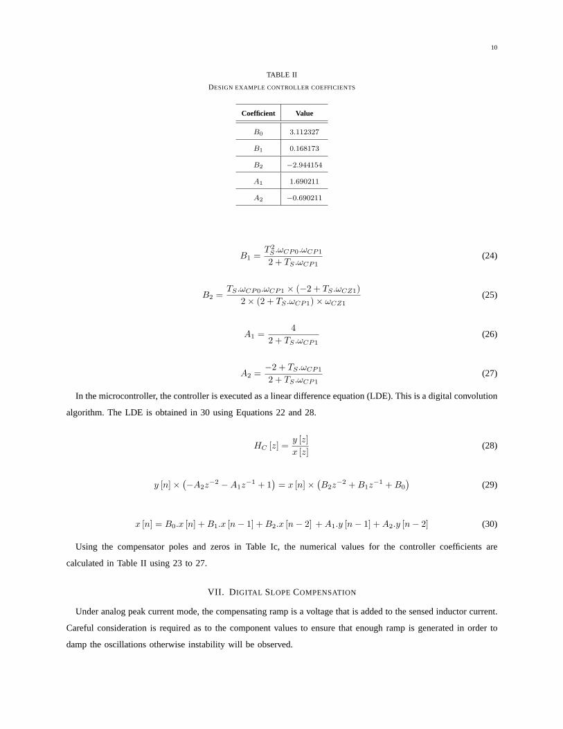
TABLE II
DESIGN EXAMPLE CONTROLLER COEFFICIENTS
Coefficient Value
B0 3.112327
B1 0.168173
B2 −2.944154
A1 1.690211
A2 −0.690211
B1 =T 2S .ωCP0.ωCP1
2 + TS .ωCP1(24)
B2 =TS .ωCP0.ωCP1 × (−2 + TS .ωCZ1)
2× (2 + TS .ωCP1)× ωCZ1(25)
A1 =4
2 + TS .ωCP1(26)
A2 =−2 + TS .ωCP1
2 + TS .ωCP1(27)
In the microcontroller, the controller is executed as a linear difference equation (LDE). This is a digital convolution
algorithm. The LDE is obtained in 30 using Equations 22 and 28.
HC [z] =y [z]
x [z](28)
y [n]× (−A2z−2 −A1z
−1 + 1)= x [n]× (
B2z−2 +B1z
−1 +B0
)(29)
x [n] = B0.x [n] +B1.x [n− 1] +B2.x [n− 2] +A1.y [n− 1] +A2.y [n− 2] (30)
Using the compensator poles and zeros in Table Ic, the numerical values for the controller coefficients are
calculated in Table II using 23 to 27.
VII. DIGITAL SLOPE COMPENSATION
Under analog peak current mode, the compensating ramp is a voltage that is added to the sensed inductor current.
Careful consideration is required as to the component values to ensure that enough ramp is generated in order to
damp the oscillations otherwise instability will be observed.

11
DACn-1(τ.t)
tDn-1.TS 'Dn-1.TS
IL(t).RI
V
Dn.TS 'Dn.TS
TS
TSLOPE
TSTART
Fig. 4. Slope compensation using a digital staircase.
Under digital peak current mode, a discrete digital ramp can be subtracted from digital output of the controller at
sub-intervals within the switching period. This task is particularly suited to the many microcontrollers on the market
which have two or more cores. The Texas Instruments TMX320F28035 used in this example has a main core and
a control law accelerator (CLA) which allows will allow the execution of both the control and slope compensation
code in parallel.
The DAC connects the output of the digital controller to the input of the continuous time comparator for peak
current detection. At the beginning of the switching period in Figure 4 the DAC module is loaded with the output
of the digital controller; the peak current reference before slope compensation. The input to the DAC is then
decremented at fixed sub-intervals throughout the switching period, simulating the compensation ramp necessary
to damp any subharmonic oscillations. This digital slope compensation is in the form of a staircase with a fixed
number of steps and step height over the switching period. Several parameters are defined to calculate the digital
slope compensation.
Ramp = VPP × 2nDAC − 1
VDAC(31)
The DAC has a specific number of bits, nDAC , which represent the output voltage range, VDAC . The peak-to-peak
compensation ramp value, VPP calculated in Section III, is converted to a discrete number using the calculation
in 31. The result is the digital staircase height. The DAC resolution can be improved by setting the external DAC
voltage reference pins VDDA and VSSA. This would be especially useful for configurations which require small
values of slope compensation.
Steps =TSLOPE
TSTEP(32)
The individual number of steps and change in height per step are calculated based on the microcontroller
specification. Several microcontroller instruction cycles will be required to decrement the input to the DAC for
each step of the staircase type compensation. The total time for each step will be specific to the microcontroller.

12
TABLE III
DIGITAL SLOPE COMPENSATION PARAMETERS
Parameter Value Parameter Value
VPP 0.621V TSTEP 50ns
nDAC 10bits TSLOPE 3950ns
VDAC 3.3V Steps 79
Ramp 192.53 ΔRamp −2.437
However, it is referred to as TSTEP for the equations herein. 32 calculates the number of discrete steps that the
microcontroller can execute for one digital slope compensation period, TSLOPE , within each switching period.
Given this, 33 calculates the change in DAC value for each step.
ΔRamp = −Ramp
Steps(33)
The digital slope compensation parameters required for the design example given in Section V are calculated
in Table III. Ideally, TSLOPE would be equal to the switching period. However, in practice it will take a number
of time steps to begin the digital slope compensation function within each switching period, TSTART . This is the
time taken for the PWM interrupt to trigger the flushing of the pipeline and start of the CLA code execution.
TSTART has been measured as 400ns on the TI microcontroller used herein.This time is comparable to the reverse
recovery time of the diode often used in the analog slope compensation circuit and forms only a small fraction of
the entire duty cycle. Therefore it has no impact on the damping of subharmonic oscillations. The time step for
the microcontroller used in this design example is 50ns. The time available for slope compensation, TSLOPE , is
calculated as 4600ns as 8 time steps are required to start the slope compensation function within each switching
period.
In Figure 5 the control-to-output transfer function of the hardware experimentation has been measured using a
frequency analyzer in order to illustrate the effectiveness of the digital staircase slope compensation. Detailed open
loop experimental results will be given in Section IX. The Figure illustrates the damping effect for different values
of ΔRamp.
The first measurement taken has no digital slope compensation, ΔRamp = 0; the DAC value remains constant
throughout the switching period. The characteristic resonant peak at half the switching frequency is visible. The
proportional gain had to be reduced such that the resonant peak did not cross the unity gain axis; allowing stable
operation and a frequency response measurement to be obtained. This does not change the shape of the magnitude
plot.
The remaining measurements are taken with digital slope compensation applied using varying values of ΔRamp.
As expected, damping of the resonant peak increases as the digital compensation ramp is increased. When ΔRamp

13
101 102 103 104 105-40
-30
-20
-10
0
10
20
Frequency (Hz)
Mag
nitu
de (d
B)
Without digital slopeWith digital slope
ΔRamp = 0 (no digital slope comp.)
ΔRamp = -1
ΔRamp = -2
ΔRamp = -3
Fig. 5. Measured control-to-output frequency response using an OMICRON Lab Bode 100 network analyzer comparing with and without digital
slope compensation for varying ΔRamp values.
tC
tDn-1.Ts 'Dn-1.Ts
V
Dn.Ts 'Dn.Ts
IL(t).RI
Zero-Order Hold
DACUpdate
SampleVOUT
Fig. 6. Time delays introduced with a digital controller. tc is the time spent sampling and performing calculations within the controler.
is between -2 and -3, the resonant peak is sufficiently damped and the converter operation is stable with the
proportional gain returned to the correct value. This indicates that the novel digital staircase implementation of
slope compensation achieves the same damping effect as analog slope compensation.
VIII. PHASE EROSION
With digital control, care must be taken to calculate the sources of delay within the system. These delays
manifests themselves as a phase margin erosion that is significant for high crossover frequencies. Therefore, with
digital control it is necessary to calculate these delays and ensure that the compensator is designed to allow for this
phase erosion.
Two factors contribute to phase erosion; the phase delay due to the sampling and calculation time [9], φCALC ,
and the phase delay due to the zero-order hold, φZOH . The sampling and calculation time begins when the output
voltage is sampled and ends when the LDE output has been calculated and is ready to be used. The output voltage
is sampled and the controller value is calculated in one period and the output of this is used in the following period.
Therefore, as illustrated in Figure 6, the sampling point should be as near to the end of the switching period as
14
possible in order to minimize this delay. Furthermore, it is up to the designer to write efficient code which minimizes
the time spent performing calculations. Ideally, the output voltage is sampled in one period and the output of the
controller is ready just before the beginning of the next period taking a total time tC .
The controller output remains fixed for the duration of the following switching period. This zero-order hold
introduces a time delay of half the switching period, TS [10]. The total time delay is the sum of the sampling
and calculation delay and the delay introduced by the zero-order hold. However, the sampled data analysis used to
derive the peak current mode model by Ridley in [2] already includes the effects of the zero-order hold. Therefore,
when using this particular peak current mode model, only the sampling and calculation delay need be considered.
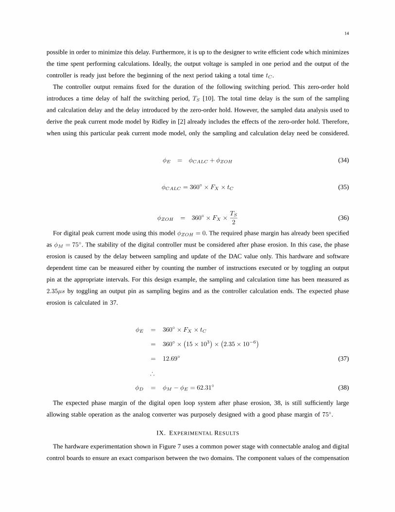
φE = φCALC + φZOH (34)
φCALC = 360◦ × FX × tC (35)
φZOH = 360◦ × FX × TS
2(36)
For digital peak current mode using this model φZOH = 0. The required phase margin has already been specified
as φM = 75◦. The stability of the digital controller must be considered after phase erosion. In this case, the phase
erosion is caused by the delay between sampling and update of the DAC value only. This hardware and software
dependent time can be measured either by counting the number of instructions executed or by toggling an output
pin at the appropriate intervals. For this design example, the sampling and calculation time has been measured as
2.35μs by toggling an output pin as sampling begins and as the controller calculation ends. The expected phase
erosion is calculated in 37.
φE = 360◦ × FX × tC
= 360◦ × (15× 103
)× (2.35× 10⁻⁶
)= 12.69◦ (37)
∴
φD = φM − φE = 62.31◦ (38)
The expected phase margin of the digital open loop system after phase erosion, 38, is still sufficiently large
allowing stable operation as the analog converter was purposely designed with a good phase margin of 75◦.
IX. EXPERIMENTAL RESULTS
The hardware experimentation shown in Figure 7 uses a common power stage with connectable analog and digital
control boards to ensure an exact comparison between the two domains. The component values of the compensation

15
Fig. 7. Peak current mode Buck converter with 16W load (bottom right), analog control board (top right) and digital control board (left).
network on the analog controller board are calculated from the compensator poles and zeros given in Table Ic. The
analog board is populated with component values nearest to those calculated for the Type II error amplifier.
The digital system is implemented using a Texas Instruments TMX320F28035 microcontroller and the precise
controller coefficients required are entered in software. This microcontroller was chosen because of its on-board
comparator, DAC and CLA modules. The CLA allows the digital slope compensation code to be executed in parallel
to the main controller. For the power stage, a Texas Instruments UCC27200 high side driver is used to drive an
IRFR3708PBF N-channel MOSFET.
Both control schemes result in stable steady state operation for varying loads. Oscilloscope plots of the transient
response of the analog and digital control methods under continuous conduction mode (CCM) are given in Figures
8 and 9 respectively. The tests are performed as the load is switched from 67% to 100% and vice versa. Automatic
switching of the load in and out of the circuit is performed by a low side MOSFET.
The output voltage (Ch4) is AC coupled and shows the controller’s response to a step change in load (Ch3). The
repetitive sawtooth shape of the output voltage is due to the product of the AC component of the output current
and the capacitor’s parasitic ESR. The transient response measurements should therefore be taken as the average
of this waveform over each switching cycle. The inductor current (Ch2) of the analog and digital systems can be
clearly seen in Figures 8b and 9b respectively. The effective regulation of the peak current by the digital controller
as the load changes is shown. The digital response in Figure 9b is almost identical to the analog response in Figure
8b.
The transient responses in Figures 8 and 9 both show a stable overdamped response with a settling time of
approximately 80μs and less than 50mV overshoot. The overdamped response is indicative of a good phase margin.
The digital transient response in Figure 9 is marginally better than the analog counterpart as the digital system has
a lower phase margin. This is due to the phase margin erosion discussed earlier.
Under discontinuous conduction mode (DCM) the control-to-output transfer function of the peak current mode
converter changes [11]. The controller has been designed to meet the crossover and phase margin specifications for
16
(a) Measured transient response of analog system.
(b) Close-up view of analog system transient response.
Fig. 8. Measured continuous conduction mode (CCM) transient response of the analog system using Tektronix TDS3014B as load is switched
from 67% (6Ω) to 100% (4Ω) and vice versa. Ch1: Switch PWM. Ch2: Output inductor current. Ch3: Load switching (high: 100%, low: 67%
load). Ch4: AC coupled output voltage.
CCM only. However it is prudent to check the transient response of the converter when operating in both CCM and
DCM modes to ensure stability and speed of response. The transient response of both analog and digital control
methods under DCM operation is shown in Figures 10a and 10b. The response is stable as the load is switched
from 1% to 10% and vice versa. The settling time under DCM has increased to approximately 300μs, due to the
change in control-to-output model, with the overshoot remaining less than 50mV .

17
(a) Measured transient response of digital system.
(b) Close-up view of digital system transient response.
Fig. 9. Measured continuous conduction mode (CCM) transient response of the digital system using Tektronix TDS3014B as load is switched
from 67% (6Ω) to 100% (4Ω) and vice versa. Ch1: Switch PWM. Ch2: Output inductor current. Ch3: Load switching (high: 100%, low: 67%
load). Ch4: AC coupled output voltage.
From the Figures, under both CCM and DCM, it can be seen that the behavior of the novel digital peak current
mode controller is equivalent to its analog counterpart as both control schemes show a similar response to the
stepped change in load.
To further confirm the suitability of the proposed digital scheme, frequency domain analysis is used. The open
loop frequency response of the converter is measured in Figure 11 using an OMICRON Lab Bode 100 vector

18
(a) Measured transient response of analog system.
(b) Measured transient response of digital system.
Fig. 10. Measured discontinuous conduction mode (DCM) transient response using Tektronix TDS3014B as load is switched from 1% (330Ω)
to 10% (38Ω).
network analyzer. Both analog and digital control methods have a 15kHz crossover frequency for fast transient
response. The measured analog phase margin of 76◦ matches the design specification and the lower digital phase
margin of 58◦ is due to the phase margin erosion. The expected digital phase margin after phase erosion calculated
in 38 was 62◦. The difference would be due to any additional delays unaccounted for within the system.
The deviations from the theoretical results at the lower frequencies are expected. In order to achieve the high
crossover frequency a large gain is required. However, in reality the gain bandwidth product of the error amplifier

19
101 102 103 104 105-20
0
20
40
60
80
100
Frequency (Hz)M
agni
tude
(dB
)
101 102 103 104 105-200
-150
-100
-50
0
Frequency (Hz)
Phas
e (D
egre
es)
TheoreticalAnalogDigital
Fig. 11. Measured open loop frequency response at full load, 16W, using an OMICRON Lab Bode 100 vector network analyzer. Crossover
frequency/phase margin: Analog 15kHz, 76◦. Digital 15kHz, 58◦.
used in the analog design will limit this gain. As the frequency increases, and the required gain reduces, the amplifier
re-enters its linear region.
An analogous effect occurs in the digital domain. Quantization errors occur in both the ADC and DAC. Further-
more, the microcontroller has a 32-bit word length and uses fixed point arithmetic resulting in additional quantization
during calculations. This, combined with the limited output range of the DAC, has the effect of limiting the low
frequency gain; similar to the gain bandwidth product limitation of the analog domain. This can result in limit cycling
if the microcontroller modules have insufficient resolution [12]. Therefore it is necessary to calculate the minimum
number of bits required for ADC, DAC (or DPWM) modules before selecting the appropriate microcontroller [13],
[14]. The results obtained during this experiment show that, in both systems, the low frequency gain is sufficiently
large for this not to be an issue.
The controller is coded such that an output pin is toggled when the subroutine starts and finishes. Figure 12 plots
the duration of the controller subroutine against the switching period. The controller occupies 26% of the switching
period leaving 74% of the MCU available to perform other tasks. As discussed in the introduction, this could
include running multiple converters, communications, condition monitoring and a user interface. This presents a
clear advantage over analog control in systems where a microcontroller is already used. Given sufficient bandwidth,
the analog control components could be removed and this task would be performed by the microcontroller already
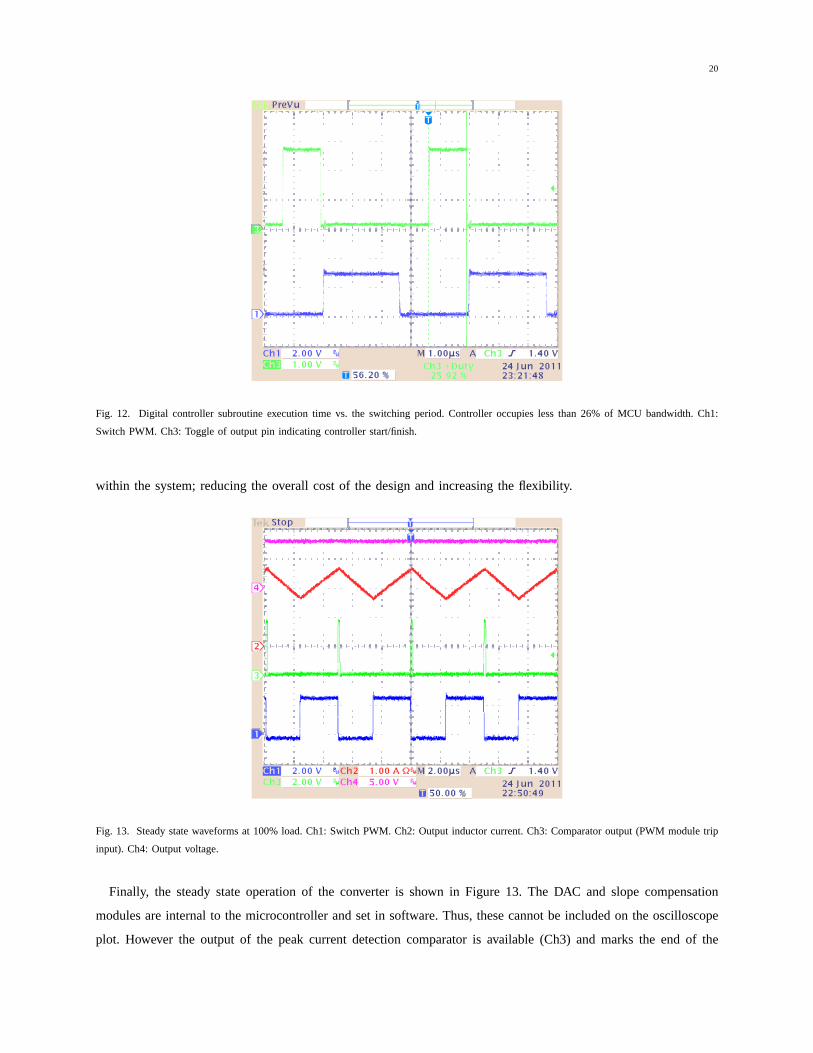
20
Fig. 12. Digital controller subroutine execution time vs. the switching period. Controller occupies less than 26% of MCU bandwidth. Ch1:
Switch PWM. Ch3: Toggle of output pin indicating controller start/finish.
within the system; reducing the overall cost of the design and increasing the flexibility.
Fig. 13. Steady state waveforms at 100% load. Ch1: Switch PWM. Ch2: Output inductor current. Ch3: Comparator output (PWM module trip
input). Ch4: Output voltage.
Finally, the steady state operation of the converter is shown in Figure 13. The DAC and slope compensation
modules are internal to the microcontroller and set in software. Thus, these cannot be included on the oscilloscope
plot. However the output of the peak current detection comparator is available (Ch3) and marks the end of the

21
PWM duty cycle (Ch1) as the switch current has reached the reference value set by the controller. The duty at full
load is 51% and no subharmonic oscillations are observed.
Figure 5 in Section VII measures the control-to-output transfer function of the hardware converter with varying
degrees of digital slope compensation. For the case where no digital slope compensation is added, ΔRamp = 0,
the system is unstable as subharmonic oscillations are observed. The resonant peak at half the switching frequency
is clearly underdamped. In the hardware experimentations presented in this Section, the digital slope compensation
method is used and the system is stable. This indicates that the novel digital staircase slope compensation method
presented in this paper is effective.
X. CONCLUSION
A new method of implementing peak current mode control using a discrete time controller, digital staircase slope
compensation and a mixed signal comparator has been described which enables cycle-by-cycle current limiting and
therefore true peak current mode operation.
Using established continuous time domain models [2], the compensator poles and zeros are analytically calculated
in the continuous time domain and converted in to the discrete time domain using the bilinear transform. The discrete
time two pole, two zero controller is implemented as a linear difference equation within the microcontroller.
A novel digital staircase ramp is used to implement the digital slope compensation required to damp subharmonic
oscillations. Experimental measurements indicate that the digital staircase has the same effect as analog slope
compensation and is accurately able to remove the resonant peak at half the switching frequency. Furthermore,
the control-to-output transfer function is measured with and without digital slope compensation. The measurement
indicates that the system will be unstable without the digital slope compensation and stable when the compensation
is added. Thus, the effectiveness of this compensation scheme is shown. Equations are given to calculate the ramp
parameters to implement this effective method of digital slope compensation.
Frequency response measurements confirm that the converter using digital control is able to match the performance
of the converter using analog control in terms of a high crossover frequency and good phase margin for this design
specification.
REFERENCES
[1] R. Ridley, B. Cho, and F. Lee, “Analysis and interpretation of loop gains of multiloop-controlled switching regulators [power supply
circuits],” Power Electronics, IEEE Transactions on, vol. 3, no. 4, pp. 489–498, Oct 1988.
[2] R. Ridley, “A new, continuous-time model for current-mode control [power convertors],” Power Electronics, IEEE Transactions on, vol. 6,
no. 2, pp. 271–280, Apr 1991.
[3] ——, “A new small-signal model for current-mode control,” Ph.D. dissertation, Virginia Polytechnic Institute and State University, 1990.
[4] V. Vorperian, “Simplified analysis of pwm converters using model of pwm switch. continuous conduction mode,” Aerospace and Electronic
Systems, IEEE Transactions on, vol. 26, no. 3, pp. 490–496, May 1990.
[5] J. Li and F. Lee, “New modeling approach and equivalent circuit representation for current-mode control,” Power Electronics, IEEE
Transactions on, vol. 25, no. 5, pp. 1218 –1230, May 2010.
[6] S.-P. Hsu, A. Brown, L. Rensink, and R. Middlebrook, “Modelling and analysis of switching dc-to-dc converters in constant-frequency
current programmed mode,” Power Electronics Specialists Conference, 1979. PESC 79. 1979 IEEE 10th Annual, pp. 284–301, 1979.

22
[7] R. D. Middlebrook, “Topics in multiple-loop regulators and current-mode programming,” Power Electronics, IEEE Transactions on, vol.
PE-2, no. 2, pp. 109–124, April 1987.
[8] J. Proakis and D. Manolakis, Digital Signal Processing. Pearson Prentice Hall, 2007.
[9] Y. Duan and H. Jin, “Digital controller design for switchmode power converters,” in Applied Power Electronics Conference and Exposition,
1999. APEC ’99. Fourteenth Annual, vol. 2, Mar. 1999, pp. 967 –973 vol.2.
[10] S. Bibian and H. Jin, “Time delay compensation of digital control for dc switchmode power supplies using prediction techniques,” Power
Electronics, IEEE Transactions on, vol. 15, no. 5, pp. 835 –842, Sep. 2000.
[11] D. Sable and R. Ridley, “Comparison of performance of single-loop and current-injection control for pwm converters that operate in both
continuous and discontinuous modes of operation,” Power Electronics, IEEE Transactions on, vol. 7, no. 1, pp. 136 –142, Jan 1992.
[12] A. Peterchev and S. Sanders, “Quantization resolution and limit cycling in digitally controlled pwm converters,” in Power Electronics
Specialists Conference, 2001. PESC. 2001 IEEE 32nd Annual, vol. 2, 2001, pp. 465 –471 vol.2.
[13] H. Peng, D. Maksimovic, A. Prodic, and E. Alarcon, “Modeling of quantization effects in digitally controlled dc-dc converters,” in Power
Electronics Specialists Conference, 2004. PESC 04. 2004 IEEE 35th Annual, vol. 6, 2004, pp. 4312 – 4318 Vol.6.
[14] A. Prodic, D. Maksimovic, and R. Erickson, “Design and implementation of a digital pwm controller for a high-frequency switching dc-dc
power converter,” in Industrial Electronics Society, 2001. IECON ’01. The 27th Annual Conference of the IEEE, vol. 2, 2001, pp. 893
–898 vol.2.
M. Hallworth (M’11) received the B.Eng. (Hons.) degree in Electronic Engineering from the University of Reading,
Reading, U.K., in 2009. Currently working towards a Ph.D. at the same University. His main research topic is in the
field of high efficiency contactless power conversion. Other related interests include power electronics, microcontrollers
and embedded systems design.
S. A. Shirsavar received the B.Eng. (Hons.) degree in Electronic Engineering and the Ph.D. degree from the University
of Reading, Reading, U.K., in 1992 and 1998, respectively. After a period of work in the industry designing embedded
controller hardware, switch-mode power supplies, and high-performance three-phase inverters, he returned to the
University of Reading as a Lecturer, where he has taught courses at all levels. His main research interests are in
power electronics and in particular digital control of switch mode power supplies.