Microcontroller with 512/1024 Bytes In-System...
169
Features • High Performance, Low Power AVR ® 8-Bit Microcontroller • Advanced RISC Architecture – 54 Powerful Instructions – Most Single Clock Cycle Execution – 16 x 8 General Purpose Working Registers – Fully Static Operation – Up to 12 MIPS Throughput at 12 MHz • Non-volatile Program and Data Memories – 512/1024 Bytes of In-System Programmable Flash Program Memory – 32 Bytes Internal SRAM – Flash Write/Erase Cycles: 10,000 – Data Retention: 20 Years at 85 o C / 100 Years at 25 o C • Peripheral Features – One 16-bit Timer/Counter with Prescaler and Two PWM Channels – Programmable Watchdog Timer with Separate On-chip Oscillator – 4-channel, 8-bit Analog to Digital Converter (1) – On-chip Analog Comparator • Special Microcontroller Features – In-System Programmable (2) – External and Internal Interrupt Sources – Low Power Idle, ADC Noise Reduction, and Power-down Modes – Enhanced Power-on Reset Circuit – Programmable Supply Voltage Level Monitor with Interrupt and Reset – Internal Calibrated Oscillator • I/O and Packages – Four Programmable I/O Lines – 6-pin SOT and 8-pad UDFN • Operating Voltage: – 1.8 – 5.5V • Programming Voltage: – 5V • Speed Grade – 0 – 4 MHz @ 1.8 – 5.5V – 0 – 8 MHz @ 2.7 – 5.5V – 0 – 12 MHz @ 4.5 – 5.5V • Industrial Temperature Range • Low Power Consumption – Active Mode: • 200μA at 1MHz and 1.8V – Idle Mode: • 25μA at 1MHz and 1.8V – Power-down Mode: • < 0.1μA at 1.8V Note: 1. The Analog to Digital Converter (ADC) is available in ATtiny5/10, only 2. At 5V, only 8-bit Microcontroller with 512/1024 Bytes In-System Programmable Flash ATtiny4/5/9/10 Preliminary Rev. 8127D–AVR–02/10
Transcript of Microcontroller with 512/1024 Bytes In-System...

8-bit Microcontroller with 512/1024 Bytes In-SystemProgrammable Flash
ATtiny4/5/9/10
Preliminary
Rev. 8127D–AVR–02/10
Features• High Performance, Low Power AVR® 8-Bit Microcontroller• Advanced RISC Architecture
– 54 Powerful Instructions – Most Single Clock Cycle Execution– 16 x 8 General Purpose Working Registers– Fully Static Operation– Up to 12 MIPS Throughput at 12 MHz
• Non-volatile Program and Data Memories– 512/1024 Bytes of In-System Programmable Flash Program Memory– 32 Bytes Internal SRAM– Flash Write/Erase Cycles: 10,000– Data Retention: 20 Years at 85oC / 100 Years at 25oC
• Peripheral Features– One 16-bit Timer/Counter with Prescaler and Two PWM Channels– Programmable Watchdog Timer with Separate On-chip Oscillator– 4-channel, 8-bit Analog to Digital Converter (1)
– On-chip Analog Comparator• Special Microcontroller Features
– In-System Programmable (2)
– External and Internal Interrupt Sources– Low Power Idle, ADC Noise Reduction, and Power-down Modes– Enhanced Power-on Reset Circuit– Programmable Supply Voltage Level Monitor with Interrupt and Reset– Internal Calibrated Oscillator
• I/O and Packages– Four Programmable I/O Lines– 6-pin SOT and 8-pad UDFN
• Operating Voltage:– 1.8 – 5.5V
• Programming Voltage:– 5V
• Speed Grade– 0 – 4 MHz @ 1.8 – 5.5V– 0 – 8 MHz @ 2.7 – 5.5V– 0 – 12 MHz @ 4.5 – 5.5V
• Industrial Temperature Range• Low Power Consumption
– Active Mode:• 200µA at 1MHz and 1.8V
– Idle Mode:• 25µA at 1MHz and 1.8V
– Power-down Mode:• < 0.1µA at 1.8V
Note: 1. The Analog to Digital Converter (ADC) is available in ATtiny5/10, only
2. At 5V, only

1. Pin Configurations
Figure 1-1. Pinout of ATtiny4/5/9/10
1.1 Pin Description
1.1.1 VCCSupply voltage.
1.1.2 GNDGround.
1.1.3 Port B (PB3..PB0)This is a 4-bit, bi-directional I/O port with internal pull-up resistors, individually selectable foreach bit. The output buffers have symmetrical drive characteristics, with both high sink andsource capability. As inputs, the port pins that are externally pulled low will source current if pull-up resistors are activated. Port pins are tri-stated when a reset condition becomes active, even ifthe clock is not running.
The port also serves the functions of various special features of the ATtiny4/5/9/10, as listed onpage 37.
1.1.4 RESETReset input. A low level on this pin for longer than the minimum pulse length will generate areset, even if the clock is not running and provided the reset pin has not been disabled. The min-imum pulse length is given in Table 16-4 on page 120. Shorter pulses are not guaranteed togenerate a reset.
The reset pin can also be used as a (weak) I/O pin.
123
654
(PCINT0/TPIDATA/OC0A/ADC0/AIN0) PB0 GND
(PCINT1/TPICLK/CLKI/ICP0/OC0B/ADC1/AIN1) PB1
PB3 (RESET/PCINT3/ADC3)VCCPB2 (T0/CLKO/PCINT2/INT0/ADC2)
SOT-23
1234
8765
(PCINT1/TPICLK/CLKI/ICP0/OC0B/ADC1/AIN1) PB1 NCNC
GND
PB2 (T0/CLKO/PCINT2/INT0/ADC2)VCCPB3 (RESET/PCINT3/ADC3)PB0 (AIN0/ADC0/OC0A/TPIDATA/PCINT0)
UDFN
28127D–AVR–02/10
ATtiny4/5/9/10

ATtiny4/5/9/10
2. OverviewATtiny4/5/9/10 are low-power CMOS 8-bit microcontrollers based on the compact AVRenhanced RISC architecture. By executing powerful instructions in a single clock cycle, theATtiny4/5/9/10 achieve throughputs approaching 1 MIPS per MHz, allowing the system designerto optimize power consumption versus processing speed.
Figure 2-1. Block Diagram
The AVR core combines a rich instruction set with 16 general purpose working registers andsystem registers. All registers are directly connected to the Arithmetic Logic Unit (ALU), allowingtwo independent registers to be accessed in one single instruction executed in one clock cycle.The resulting architecture is compact and code efficient while achieving throughputs up to tentimes faster than conventional CISC microcontrollers.
STACKPOINTER
SRAM
PROGRAMCOUNTER
PROGRAMMINGLOGIC
ISPINTERFACE
INTERNALOSCILLATOR
WATCHDOGTIMER
RESET FLAGREGISTER
MCU STATUSREGISTER
TIMER/COUNTER0
CALIBRATEDOSCILLATOR
TIMING ANDCONTROL
INTERRUPTUNIT
ANALOGCOMPARATOR ADC
GENERALPURPOSE
REGISTERS
XYZ
ALU
STATUSREGISTER
PROGRAMFLASH
INSTRUCTIONREGISTER
INSTRUCTIONDECODER
CONTROLLINES
VCC RESET
DATA REGISTERPORT B
DIRECTIONREG. PORT B
DRIVERSPORT B
GNDPB3:0
8-BIT DATA BUS
38127D–AVR–02/10

The ATtiny4/5/9/10 provide the following features: 512/1024 byte of In-System ProgrammableFlash, 32 bytes of SRAM, four general purpose I/O lines, 16 general purpose working registers,a 16-bit timer/counter with two PWM channels, internal and external interrupts, a programmablewatchdog timer with internal oscillator, an internal calibrated oscillator, and four software select-able power saving modes. ATtiny5/10 are also equipped with a four-channel, 8-bit Analog toDigital Converter (ADC).
Idle mode stops the CPU while allowing the SRAM, timer/counter, ADC (ATtiny5/10, only), ana-log comparator, and interrupt system to continue functioning. ADC Noise Reduction modeminimizes switching noise during ADC conversions by stopping the CPU and all I/O modulesexcept the ADC. In Power-down mode registers keep their contents and all chip functions aredisabled until the next interrupt or hardware reset. In Standby mode, the oscillator is runningwhile the rest of the device is sleeping, allowing very fast start-up combined with low powerconsumption.
The device is manufactured using Atmel’s high density non-volatile memory technology. The on-chip, in-system programmable Flash allows program memory to be re-programmed in-system bya conventional, non-volatile memory programmer.
The ATtiny4/5/9/10 AVR are supported by a suite of program and system development tools,including macro assemblers and evaluation kits.
2.1 Comparison of ATtiny4, ATtiny5, ATtiny9 and ATtiny10A comparison of the devices is shown in Table 2-1.
Table 2-1. Differences between ATtiny4, ATtiny5, ATtiny9 and ATtiny10
Device Flash ADC Signature
ATtiny4 512 bytes No 0x1E 0x8F 0x0A
ATtiny5 512 bytes Yes 0x1E 0x8F 0x09
ATtiny9 1024 bytes No 0x1E 0x90 0x08
ATtiny10 1024 bytes Yes 0x1E 0x90 0x03
48127D–AVR–02/10
ATtiny4/5/9/10

ATtiny4/5/9/10
3. General Information
3.1 ResourcesA comprehensive set of drivers, application notes, data sheets and descriptions on developmenttools are available for download at http://www.atmel.com/avr.
3.2 Code ExamplesThis documentation contains simple code examples that briefly show how to use various parts ofthe device. These code examples assume that the part specific header file is included beforecompilation. Be aware that not all C compiler vendors include bit definitions in the header filesand interrupt handling in C is compiler dependent. Please confirm with the C compiler documen-tation for more details.
3.3 Data RetentionReliability Qualification results show that the projected data retention failure rate is much lessthan 1 PPM over 20 years at 85°C or 100 years at 25°C.
3.4 DisclaimerTypical values contained in this datasheet are based on simulations and characterization ofother AVR microcontrollers manufactured on the same process technology. Min and Max valueswill be available after the device has been characterized.
58127D–AVR–02/10

4. CPU CoreThis section discusses the AVR core architecture in general. The main function of the CPU coreis to ensure correct program execution. The CPU must therefore be able to access memories,perform calculations, control peripherals, and handle interrupts.
4.1 Architectural Overview
Figure 4-1. Block Diagram of the AVR Architecture
In order to maximize performance and parallelism, the AVR uses a Harvard architecture – withseparate memories and buses for program and data. Instructions in the program memory areexecuted with a single level pipelining. While one instruction is being executed, the next instruc-tion is pre-fetched from the program memory. This concept enables instructions to be executedin every clock cycle. The program memory is In-System Reprogrammable Flash memory.
The fast-access Register File contains 16 x 8-bit general purpose working registers with a singleclock cycle access time. This allows single-cycle Arithmetic Logic Unit (ALU) operation. In a typ-ical ALU operation, two operands are output from the Register File, the operation is executed,and the result is stored back in the Register File – in one clock cycle.
FlashProgramMemory
InstructionRegister
InstructionDecoder
ProgramCounter
Control Lines
16 x 8GeneralPurpose
Registrers
ALU
Statusand Control
I/O Lines
Data Bus 8-bit
DataSRAM
Dire
ct A
ddre
ssin
g
Indi
rect
Add
ress
ing
InterruptUnit
WatchdogTimer
AnalogComparator
Timer/Counter 0
ADC
68127D–AVR–02/10
ATtiny4/5/9/10

ATtiny4/5/9/10
Six of the 16 registers can be used as three 16-bit indirect address register pointers for dataspace addressing – enabling efficient address calculations. One of the these address pointerscan also be used as an address pointer for look up tables in Flash program memory. Theseadded function registers are the 16-bit X-, Y-, and Z-register, described later in this section.
The ALU supports arithmetic and logic operations between registers or between a constant anda register. Single register operations can also be executed in the ALU. After an arithmetic opera-tion, the Status Register is updated to reflect information about the result of the operation.
Program flow is provided by conditional and unconditional jump and call instructions, capable ofdirectly addressing the whole address space. Most AVR instructions have a single 16-bit wordformat but 32-bit wide instructions also exist. The actual instruction set varies, as some devicesonly implement a part of the instruction set.
During interrupts and subroutine calls, the return address Program Counter (PC) is stored on theStack. The Stack is effectively allocated in the general data SRAM, and consequently the Stacksize is only limited by the SRAM size and the usage of the SRAM. All user programs must initial-ize the SP in the Reset routine (before subroutines or interrupts are executed). The StackPointer (SP) is read/write accessible in the I/O space. The data SRAM can easily be accessedthrough the four different addressing modes supported in the AVR architecture.
The memory spaces in the AVR architecture are all linear and regular memory maps.
A flexible interrupt module has its control registers in the I/O space with an additional GlobalInterrupt Enable bit in the Status Register. All interrupts have a separate Interrupt Vector in theInterrupt Vector table. The interrupts have priority in accordance with their Interrupt Vector posi-tion. The lower the Interrupt Vector address, the higher the priority.
The I/O memory space contains 64 addresses for CPU peripheral functions as Control Regis-ters, SPI, and other I/O functions. The I/O memory can be accessed as the data space locations,0x0000 - 0x003F.
4.2 ALU – Arithmetic Logic UnitThe high-performance AVR ALU operates in direct connection with all the 16 general purposeworking registers. Within a single clock cycle, arithmetic operations between general purposeregisters or between a register and an immediate are executed. The ALU operations are dividedinto three main categories – arithmetic, logical, and bit-functions. Some implementations of thearchitecture also provide a powerful multiplier supporting both signed/unsigned multiplicationand fractional format. See document “AVR Instruction Set” and section “Instruction Set Sum-mary” on page 152 for a detailed description.
4.3 Status RegisterThe Status Register contains information about the result of the most recently executed arithme-tic instruction. This information can be used for altering program flow in order to performconditional operations. Note that the Status Register is updated after all ALU operations, asspecified in document “AVR Instruction Set” and section “Instruction Set Summary” on page152. This will in many cases remove the need for using the dedicated compare instructions,resulting in faster and more compact code.
The Status Register is not automatically stored when entering an interrupt routine and restoredwhen returning from an interrupt. This must be handled by software.
78127D–AVR–02/10
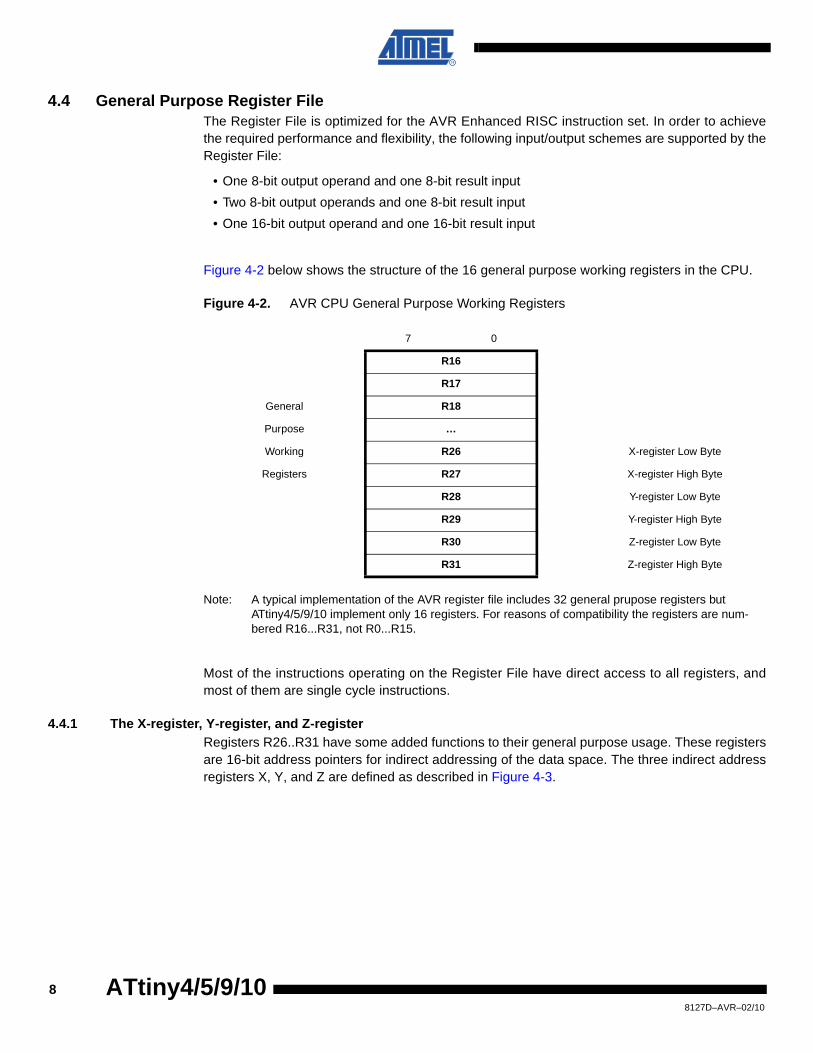
4.4 General Purpose Register FileThe Register File is optimized for the AVR Enhanced RISC instruction set. In order to achievethe required performance and flexibility, the following input/output schemes are supported by theRegister File:
• One 8-bit output operand and one 8-bit result input
• Two 8-bit output operands and one 8-bit result input
• One 16-bit output operand and one 16-bit result input
Figure 4-2 below shows the structure of the 16 general purpose working registers in the CPU.
Figure 4-2. AVR CPU General Purpose Working Registers
Note: A typical implementation of the AVR register file includes 32 general prupose registers but ATtiny4/5/9/10 implement only 16 registers. For reasons of compatibility the registers are num-bered R16...R31, not R0...R15.
Most of the instructions operating on the Register File have direct access to all registers, andmost of them are single cycle instructions.
4.4.1 The X-register, Y-register, and Z-registerRegisters R26..R31 have some added functions to their general purpose usage. These registersare 16-bit address pointers for indirect addressing of the data space. The three indirect addressregisters X, Y, and Z are defined as described in Figure 4-3.
7 0
R16
R17
General R18
Purpose …
Working R26 X-register Low Byte
Registers R27 X-register High Byte
R28 Y-register Low Byte
R29 Y-register High Byte
R30 Z-register Low Byte
R31 Z-register High Byte
88127D–AVR–02/10
ATtiny4/5/9/10

ATtiny4/5/9/10
Figure 4-3. The X-, Y-, and Z-registers
In different addressing modes these address registers function as automatic increment andautomatic decrement (see document “AVR Instruction Set” and section “Instruction Set Sum-mary” on page 152 for details).
4.5 Stack PointerThe Stack is mainly used for storing temporary data, for storing local variables and for storingreturn addresses after interrupts and subroutine calls. The Stack Pointer Register always pointsto the top of the Stack. Note that the Stack is implemented as growing from higher memory loca-tions to lower memory locations. This implies that a Stack PUSH command decreases the StackPointer.
The Stack Pointer points to the data SRAM Stack area where the Subroutine and InterruptStacks are located. This Stack space in the data SRAM must be defined by the program beforeany subroutine calls are executed or interrupts are enabled. The Stack Pointer must be set topoint above 0x40. The Stack Pointer is decremented by one when data is pushed onto the Stackwith the PUSH instruction, and it is decremented by two when the return address is pushed ontothe Stack with subroutine call or interrupt. The Stack Pointer is incremented by one when data ispopped from the Stack with the POP instruction, and it is incremented by two when data ispopped from the Stack with return from subroutine RET or return from interrupt RETI.
The AVR Stack Pointer is implemented as two 8-bit registers in the I/O space. The number ofbits actually used is implementation dependent. Note that the data space in some implementa-tions of the AVR architecture is so small that only SPL is needed. In this case, the SPH Registerwill not be present.
4.6 Instruction Execution TimingThis section describes the general access timing concepts for instruction execution. The AVRCPU is driven by the CPU clock clkCPU, directly generated from the selected clock source for thechip. No internal clock division is used.
15 XH XL 0
X-register 7 0 7 0
R27 R26
15 YH YL 0
Y-register 7 0 7 0
R29 R28
15 ZH ZL 0
Z-register 7 0 7 0
R31 R30
98127D–AVR–02/10

Figure 4-4. The Parallel Instruction Fetches and Instruction Executions
Figure 4-4 shows the parallel instruction fetches and instruction executions enabled by the Har-vard architecture and the fast access Register File concept. This is the basic pipelining conceptto obtain up to 1 MIPS per MHz with the corresponding unique results for functions per cost,functions per clocks, and functions per power-unit.
Figure 4-5 shows the internal timing concept for the Register File. In a single clock cycle an ALUoperation using two register operands is executed, and the result is stored back to the destina-tion register.
Figure 4-5. Single Cycle ALU Operation
4.7 Reset and Interrupt HandlingThe AVR provides several different interrupt sources. These interrupts and the separate ResetVector each have a separate Program Vector in the program memory space. All interrupts areassigned individual enable bits which must be written logic one together with the Global InterruptEnable bit in the Status Register in order to enable the interrupt.
The lowest addresses in the program memory space are by default defined as the Reset andInterrupt Vectors. The complete list of vectors is shown in “Interrupts” on page 36. The list alsodetermines the priority levels of the different interrupts. The lower the address the higher is thepriority level. RESET has the highest priority, and next is INT0 – the External Interrupt Request0.
When an interrupt occurs, the Global Interrupt Enable I-bit is cleared and all interrupts are dis-abled. The user software can write logic one to the I-bit to enable nested interrupts. All enabled
clk
1st Instruction Fetch
1st Instruction Execute2nd Instruction Fetch
2nd Instruction Execute3rd Instruction Fetch
3rd Instruction Execute4th Instruction Fetch
T1 T2 T3 T4
CPU
Total Execution Time
Register Operands Fetch
ALU Operation Execute
Result Write Back
T1 T2 T3 T4
clkCPU
108127D–AVR–02/10
ATtiny4/5/9/10

ATtiny4/5/9/10
interrupts can then interrupt the current interrupt routine. The I-bit is automatically set when aReturn from Interrupt instruction – RETI – is executed.
There are basically two types of interrupts. The first type is triggered by an event that sets theInterrupt Flag. For these interrupts, the Program Counter is vectored to the actual Interrupt Vec-tor in order to execute the interrupt handling routine, and hardware clears the correspondingInterrupt Flag. Interrupt Flags can also be cleared by writing a logic one to the flag bit position(s)to be cleared. If an interrupt condition occurs while the corresponding interrupt enable bit iscleared, the Interrupt Flag will be set and remembered until the interrupt is enabled, or the flag iscleared by software. Similarly, if one or more interrupt conditions occur while the Global InterruptEnable bit is cleared, the corresponding Interrupt Flag(s) will be set and remembered until theGlobal Interrupt Enable bit is set, and will then be executed by order of priority.
The second type of interrupts will trigger as long as the interrupt condition is present. Theseinterrupts do not necessarily have Interrupt Flags. If the interrupt condition disappears before theinterrupt is enabled, the interrupt will not be triggered.
When the AVR exits from an interrupt, it will always return to the main program and execute onemore instruction before any pending interrupt is served.
Note that the Status Register is not automatically stored when entering an interrupt routine, norrestored when returning from an interrupt routine. This must be handled by software.
When using the CLI instruction to disable interrupts, the interrupts will be immediately disabled.No interrupt will be executed after the CLI instruction, even if it occurs simultaneously with theCLI instruction.
When using the SEI instruction to enable interrupts, the instruction following SEI will be exe-cuted before any pending interrupts, as shown in the following example.
Note: See “Code Examples” on page 5.
4.7.1 Interrupt Response TimeThe interrupt execution response for all the enabled AVR interrupts is four clock cycles mini-mum. After four clock cycles the Program Vector address for the actual interrupt handling routineis executed. During this four clock cycle period, the Program Counter is pushed onto the Stack.The vector is normally a jump to the interrupt routine, and this jump takes three clock cycles. Ifan interrupt occurs during execution of a multi-cycle instruction, this instruction is completedbefore the interrupt is served. If an interrupt occurs when the MCU is in sleep mode, the interruptexecution response time is increased by four clock cycles. This increase comes in addition to thestart-up time from the selected sleep mode.
A return from an interrupt handling routine takes four clock cycles. During these four clockcycles, the Program Counter (two bytes) is popped back from the Stack, the Stack Pointer isincremented by two, and the I-bit in SREG is set.
Assembly Code Example
sei ; set Global Interrupt Enable
sleep ; enter sleep, waiting for interrupt
; note: will enter sleep before any pending interrupt(s)
118127D–AVR–02/10

4.8 Register Description
4.8.1 CCP – Configuration Change Protection Register
• Bits 7:0 – CCP[7:0] – Configuration Change ProtectionIn order to change the contents of a protected I/O register the CCP register must first be writtenwith the correct signature. After CCP is written the protected I/O registers may be written to dur-ing the next four CPU instruction cycles. All interrupts are ignored during these cycles. Afterthese cycles interrupts are automatically handled again by the CPU, and any pending interruptswill be executed according to their priority.
When the protected I/O register signature is written, CCP[0] will read as one as long as the pro-tected feature is enabled, while CCP[7:1] will always read as zero.
Table 4-1 shows the signatures that are in recognised.
4.8.2 SPH and SPL — Stack Pointer Register
4.8.3 SREG – Status Register
• Bit 7 – I: Global Interrupt EnableThe Global Interrupt Enable bit must be set for the interrupts to be enabled. The individual inter-rupt enable control is then performed in separate control registers. If the Global Interrupt EnableRegister is cleared, none of the interrupts are enabled independent of the individual interruptenable settings. The I-bit is cleared by hardware after an interrupt has occurred, and is set bythe RETI instruction to enable subsequent interrupts. The I-bit can also be set and cleared bythe application with the SEI and CLI instructions, as described in the document “AVR InstructionSet” and “Instruction Set Summary” on page 152.
Bit 7 6 5 4 3 2 1 0
0x3C CCP[7:0] CCP
Read/Write W W W W W W W W
Initial Value 0 0 0 0 0 0 0 0
Table 4-1. Signatures Recognised by the Configuration Change Protection Register
Signature Group Description
0xD8 IOREG: CLKMSR, CLKPSR, WDTCSR Protected I/O register
Bit 15 14 13 12 11 10 9 8
0x3E SP15 SP14 SP13 SP12 SP11 SP10 SP9 SP8 SPH
0x3D SP7 SP6 SP5 SP4 SP3 SP2 SP1 SP0 SPL
7 6 5 4 3 2 1 0
Read/Write R/W R/W R/W R/W R/W R/W R/W R/W
Read/Write R/W R/W R/W R/W R/W R/W R/W R/W
Initial Value RAMEND RAMEND RAMEND RAMEND RAMEND RAMEND RAMEND RAMEND
Initial Value RAMEND RAMEND RAMEND RAMEND RAMEND RAMEND RAMEND RAMEND
Bit 7 6 5 4 3 2 1 0
0x3F I T H S V N Z C SREG
Read/Write R/W R/W R/W R/W R/W R/W R/W R/W
Initial Value 0 0 0 0 0 0 0 0
128127D–AVR–02/10
ATtiny4/5/9/10

ATtiny4/5/9/10
• Bit 6 – T: Bit Copy StorageThe Bit Copy instructions BLD (Bit LoaD) and BST (Bit STore) use the T-bit as source or desti-nation for the operated bit. A bit from a register in the Register File can be copied into T by theBST instruction, and a bit in T can be copied into a bit in a register in the Register File by theBLD instruction.
• Bit 5 – H: Half Carry Flag The Half Carry Flag H indicates a Half Carry in some arithmetic operations. Half Carry is usefulin BCD arithmetic. See document “AVR Instruction Set” and section “Instruction Set Summary”on page 152 for detailed information.
• Bit 4 – S: Sign Bit, S = N ⊕ VThe S-bit is always an exclusive or between the Negative Flag N and the Two’s ComplementOverflow Flag V. See document “AVR Instruction Set” and section “Instruction Set Summary” onpage 152 for detailed information.
• Bit 3 – V: Two’s Complement Overflow FlagThe Two’s Complement Overflow Flag V supports two’s complement arithmetics. See document“AVR Instruction Set” and section “Instruction Set Summary” on page 152 for detailedinformation.
• Bit 2 – N: Negative FlagThe Negative Flag N indicates a negative result in an arithmetic or logic operation. See docu-ment “AVR Instruction Set” and section “Instruction Set Summary” on page 152 for detailedinformation.
• Bit 1 – Z: Zero FlagThe Zero Flag Z indicates a zero result in an arithmetic or logic operation. See document “AVRInstruction Set” and section “Instruction Set Summary” on page 152 for detailed information.
• Bit 0 – C: Carry FlagThe Carry Flag C indicates a carry in an arithmetic or logic operation. See document “AVRInstruction Set” and section “Instruction Set Summary” on page 152 for detailed information.
138127D–AVR–02/10

5. MemoriesThis section describes the different memories in the ATtiny4/5/9/10. Devices have two mainmemory areas, the program memory space and the data memory space.
5.1 In-System Re-programmable Flash Program MemoryThe ATtiny4/5/9/10 contain 512/1024 bytes of on-chip, in-system reprogrammable Flash mem-ory for program storage. Since all AVR instructions are 16 or 32 bits wide, the Flash is organizedas 256/512 x 16.
The Flash memory has an endurance of at least 10,000 write/erase cycles. The ATtiny4/5/9/10Program Counter (PC) is 9 bits wide, thus capable of addressing the 256/512 program memorylocations, starting at 0x000. “Memory Programming” on page 108 contains a detailed descriptionon Flash data serial downloading.
Constant tables can be allocated within the entire address space of program memory. Since pro-gram memory can not be accessed directly, it has been mapped to the data memory. Themapped program memory begins at byte address 0x4000 in data memory (see Figure 5-1 onpage 15). Although programs are executed starting from address 0x000 in program memory itmust be addressed starting from 0x4000 when accessed via the data memory.
Internal write operations to Flash program memory have been disabled and program memorytherefore appears to firmware as read-only. Flash memory can still be written to externally butinternal write operations to the program memory area will not be succesful.
Timing diagrams of instruction fetch and execution are presented in “Instruction Execution Tim-ing” on page 9.
5.2 Data MemoryData memory locations include the I/O memory, the internal SRAM memory, the non-volatilememory lock bits, and the Flash memory. See Figure 5-1 on page 15 for an illustration on howthe ATtiny4/5/9/10 memory space is organized.
The first 64 locations are reserved for I/O memory, while the following 32 data memory locationsaddress the internal data SRAM.
The non-volatile memory lock bits and all the Flash memory sections are mapped to the datamemory space. These locations appear as read-only for device firmware.
The four different addressing modes for data memory are direct, indirect, indirect with pre-decre-ment, and indirect with post-increment. In the register file, registers R26 to R31 function aspointer registers for indirect addressing.
The IN and OUT instructions can access all 64 locations of I/O memory. Direct addressing usingthe LDS and STS instructions reaches the 128 locations between 0x0040 and 0x00BF.
The indirect addressing reaches the entire data memory space. When using indirect addressingmodes with automatic pre-decrement and post-increment, the address registers X, Y, and Z aredecremented or incremented.
148127D–AVR–02/10
ATtiny4/5/9/10

ATtiny4/5/9/10
Figure 5-1. Data Memory Map (Byte Addressing)
5.2.1 Data Memory Access TimesThis section describes the general access timing concepts for internal memory access. Theinternal data SRAM access is performed in two clkCPU cycles as described in Figure 5-2.
Figure 5-2. On-chip Data SRAM Access Cycles
0x0000 ... 0x003F
0x0040 ... 0x005F
0x0060 ... 0x3EFF
0x3F00 ... 0x3F01
0x3F02 ... 0x3F3F
0x3F40 ... 0x3F41
0x3F42 ... 0x3F7F
0x3F80 ... 0x3F81
0x3F82 ... 0x3FBF
0x3FC0 ... 0x3FC3
0x3FC4 ... 0x3FFF
0x4000 ... 0x41FF/0x43FF
0x4400 ... 0xFFFF
I/O SPACE
SRAM DATA MEMORY
(reserved)
NVM LOCK BITS
(reserved)
CONFIGURATION BITS
(reserved)
CALIBRATION BITS
(reserved)
DEVICE ID BITS
(reserved)
FLASH PROGRAM MEMORY
(reserved)
clk
WR
RD
Data
Data
Address Address valid
T1 T2 T3
Compute Address
Rea
dW
rite
CPU
Memory Access Instruction Next Instruction
158127D–AVR–02/10

5.3 I/O MemoryThe I/O space definition of the ATtiny4/5/9/10 is shown in “Register Summary” on page 150.
All ATtiny4/5/9/10 I/Os and peripherals are placed in the I/O space. All I/O locations may beaccessed using the LD and ST instructions, enabling data transfer between the 16 general pur-pose working registers and the I/O space. I/O Registers within the address range 0x00 - 0x1Fare directly bit-accessible using the SBI and CBI instructions. In these registers, the value of sin-gle bits can be checked by using the SBIS and SBIC instructions. See document “AVRInstruction Set” and section “Instruction Set Summary” on page 152 for more details. Whenusing the I/O specific commands IN and OUT, the I/O addresses 0x00 - 0x3F must be used.
For compatibility with future devices, reserved bits should be written to zero if accessed.Reserved I/O memory addresses should never be written.
Some of the status flags are cleared by writing a logical one to them. Note that CBI and SBIinstructions will only operate on the specified bit, and can therefore be used on registers contain-ing such status flags. The CBI and SBI instructions work on registers in the address range 0x00to 0x1F, only.
The I/O and Peripherals Control Registers are explained in later sections.
168127D–AVR–02/10
ATtiny4/5/9/10

ATtiny4/5/9/10
6. Clock SystemFigure 6-1 presents the principal clock systems and their distribution in ATtiny4/5/9/10. All of theclocks need not be active at a given time. In order to reduce power consumption, the clocks tomodules not being used can be halted by using different sleep modes and power reduction reg-ister bits, as described in “Power Management and Sleep Modes” on page 23. The clocksystems is detailed below.
Figure 6-1. Clock Distribution
6.1 Clock SubsystemsThe clock subsystems are detailed in the sections below.
6.1.1 CPU Clock – clkCPU
The CPU clock is routed to parts of the system concerned with operation of the AVR Core.Examples of such modules are the General Purpose Register File, the System Registers andthe SRAM data memory. Halting the CPU clock inhibits the core from performing general opera-tions and calculations.
6.1.2 I/O Clock – clkI/O
The I/O clock is used by the majority of the I/O modules, like Timer/Counter. The I/O clock isalso used by the External Interrupt module, but note that some external interrupts are detectedby asynchronous logic, allowing such interrupts to be detected even if the I/O clock is halted.
6.1.3 NVM clock - clkNVM
The NVM clock controls operation of the Non-Volatile Memory Controller. The NVM clock is usu-ally active simultaneously with the CPU clock.
CLOCK CONTROL UNIT
GENERALI/O MODULES
ANALOG-TO-DIGITALCONVERTER
CPUCORE
WATCHDOGTIMER
RESETLOGIC
CLOCKPRESCALER
RAM
CLOCKSWITCH
NVM
CALIBRATEDOSCILLATOR
clk ADC
SOURCE CLOCK
clk I/Oclk CPU
clk NVM
WATCHDOGCLOCK
WATCHDOGOSCILLATOR
EXTERNALCLOCK
178127D–AVR–02/10

6.1.4 ADC Clock – clkADC
The ADC is provided with a dedicated clock domain. This allows halting the CPU and I/O clocksin order to reduce noise generated by digital circuitry. This gives more accurate ADC conversionresults.
The ADC is available in ATtiny5/10, only.
6.2 Clock SourcesAll synchronous clock signals are derived from the main clock. The device has three alternativesources for the main clock, as follows:
• Calibrated Internal 8 MHz Oscillator (see page 18)
• External Clock (see page 18)
• Internal 128 kHz Oscillator (see page 19)
See Table 6-3 on page 21 on how to select and change the active clock source.
6.2.1 Calibrated Internal 8 MHz OscillatorThe calibrated internal oscillator provides an approximately 8 MHz clock signal. Though voltageand temperature dependent, this clock can be very accurately calibrated by the user. See Table16-2 on page 119, Figure 17-39 on page 143 and Figure 17-40 on page 143 for more details.
This clock may be selected as the main clock by setting the Clock Main Select bits CLKMS[1:0]in CLKMSR to 0b00. Once enabled, the oscillator will operate with no external components. Dur-ing reset, hardware loads the calibration byte into the OSCCAL register and therebyautomatically calibrates the oscillator. The accuracy of this calibration is shown as Factory cali-bration in Table 16-2 on page 119.
When this oscillator is used as the main clock, the watchdog oscillator will still be used for thewatchdog timer and reset time-out. For more information on the pre-programmed calibrationvalue, see section “Calibration Section” on page 111.
6.2.2 External ClockTo use the device with an external clock source, CLKI should be driven as shown in Figure 6-2.The external clock is selected as the main clock by setting CLKMS[1:0] bits in CLKMSR to 0b10.
Figure 6-2. External Clock Drive Configuration
When applying an external clock, it is required to avoid sudden changes in the applied clock fre-quency to ensure stable operation of the MCU. A variation in frequency of more than 2% fromone clock cycle to the next can lead to unpredictable behavior. It is required to ensure that theMCU is kept in reset during such changes in the clock frequency.
EXTERNALCLOCKSIGNAL
CLKI
GND
188127D–AVR–02/10
ATtiny4/5/9/10

ATtiny4/5/9/10
6.2.3 Internal 128 kHz OscillatorThe internal 128 kHz oscillator is a low power oscillator providing a clock of 128 kHz. The fre-quency depends on supply voltage, temperature and batch variations. This clock may be selectas the main clock by setting the CLKMS[1:0] bits in CLKMSR to 0b01.
6.2.4 Switching Clock SourceThe main clock source can be switched at run-time using the “CLKMSR – Clock Main SettingsRegister” on page 21. When switching between any clock sources, the clock system ensuresthat no glitch occurs in the main clock.
6.2.5 Default Clock SourceThe calibrated internal 8 MHz oscillator is always selected as main clock when the device ispowered up or has been reset. The synchronous system clock is the main clock divided by 8,controlled by the System Clock Prescaler. The Clock Prescaler Select Bits can be written later tochange the system clock frequency. See “System Clock Prescaler”.
6.3 System Clock PrescalerThe system clock is derived from the main clock via the System Clock Prescaler. The systemclock can be divided by setting the “CLKPSR – Clock Prescale Register” on page 22. The sys-tem clock prescaler can be used to decrease power consumption at times when requirementsfor processing power is low or to bring the system clock within limits of maximum frequency. Theprescaler can be used with all main clock source options, and it will affect the clock frequency ofthe CPU and all synchronous peripherals.
The System Clock Prescaler can be used to implement run-time changes of the internal clockfrequency while still ensuring stable operation.
6.3.1 Switching Prescaler SettingWhen switching between prescaler settings, the system clock prescaler ensures that no glitchoccurs in the system clock and that no intermediate frequency is higher than neither the clockfrequency corresponding the previous setting, nor the clock frequency corresponding to the newsetting.
The ripple counter that implements the prescaler runs at the frequency of the main clock, whichmay be faster than the CPU's clock frequency. Hence, it is not possible to determine the state ofthe prescaler - even if it were readable, and the exact time it takes to switch from one clock divi-sion to another cannot be exactly predicted.
From the time the CLKPS values are written, it takes between T1 + T2 and T1 + 2*T2 before thenew clock frequency is active. In this interval, two active clock edges are produced. Here, T1 isthe previous clock period, and T2 is the period corresponding to the new prescaler setting.
198127D–AVR–02/10

6.4 Starting
6.4.1 Starting from ResetThe internal reset is immediately asserted when a reset source goes active. The internal reset iskept asserted until the reset source is released and the start-up sequence is completed. Thestart-up sequence includes three steps, as follows.
1. The first step after the reset source has been released consists of the device counting the reset start-up time. The purpose of this reset start-up time is to ensure that supply voltage has reached sufficient levels. The reset start-up time is counted using the inter-nal 128 kHz oscillator. See Table 6-1 for details of reset start-up time.Note that the actual supply voltage is not monitored by the start-up logic. The device will count until the reset start-up time has elapsed even if the device has reached suffi-cient supply voltage levels earlier.
2. The second step is to count the oscillator start-up time, which ensures that the cali-brated internal oscillator has reached a stable state before it is used by the other parts of the system. The calibrated internal oscillator needs to oscillate for a minimum num-ber of cycles before it can be considered stable. See Table 6-1 for details of the oscillator start-up time.
3. The last step before releasing the internal reset is to load the calibration and the config-uration values from the Non-Volatile Memory to configure the device properly. The configuration time is listed in Table 6-1.
Notes: 1. After powering up the device or after a reset the system clock is automatically set to calibrated internal 8 MHz oscillator, divided by 8
6.4.2 Starting from Power-Down ModeWhen waking up from Power-Down sleep mode, the supply voltage is assumed to be at a suffi-cient level and only the oscillator start-up time is counted to ensure the stable operation of theoscillator. The oscillator start-up time is counted on the selected main clock, and the start-uptime depends on the clock selected. See Table 6-2 for details.
Notes: 1. The start-up time is measured in main clock oscillator cycles.
6.4.3 Starting from Idle / ADC Noise Reduction / Standby ModeWhen waking up from Idle, ADC Noise Reduction or Standby Mode, the oscillator is already run-ning and no oscillator start-up time is introduced.
The ADC is available in ATtiny5/10, only.
Table 6-1. Start-up Times when Using the Internal Calibrated Oscillator
Reset Oscillator Configuration Total start-up time
64 ms 6 cycles 21 cycles 64 ms + 6 oscillator cycles + 21 system clock cycles (1)
Table 6-2. Start-up Time from Power-Down Sleep Mode.
Oscillator start-up time Total start-up time
6 cycles 6 oscillator cycles (1)
208127D–AVR–02/10
ATtiny4/5/9/10

ATtiny4/5/9/10
6.5 Register Description
6.5.1 CLKMSR – Clock Main Settings Register
• Bit 7:2 – Res: Reserved BitsThese bits are reserved and always read zero.
• Bit 1:0 – CLKMS[1:0]: Clock Main Select BitsThese bits select the main clock source of the system. The bits can be written at run-time toswitch the source of the main clock. The clock system ensures glitch free switching of the mainclock source.
The main clock alternatives are shown in Table 6-3.
To avoid unintentional switching of main clock source, a protected change sequence must befollowed to change the CLKMS bits, as follows:
1. Write the signature for change enable of protected I/O register to register CCP
2. Within four instruction cycles, write the CLKMS bits with the desired value
6.5.2 OSCCAL – Oscillator Calibration Register.
• Bits 7:0 – CAL[7:0]: Oscillator Calibration ValueThe oscillator calibration register is used to trim the calibrated internal oscillator and remove pro-cess variations from the oscillator frequency. A pre-programmed calibration value isautomatically written to this register during chip reset, giving the factory calibrated frequency asspecified in Table 16-2, “Calibration Accuracy of Internal RC Oscillator,” on page 119.
The application software can write this register to change the oscillator frequency. The oscillatorcan be calibrated to frequencies as specified in Table 16-2, “Calibration Accuracy of Internal RCOscillator,” on page 119. Calibration outside the range given is not guaranteed.
The CAL[7:0] bits are used to tune the frequency of the oscillator. A setting of 0x00 gives thelowest frequency, and a setting of 0xFF gives the highest frequency.
Bit 7 6 5 4 3 2 1 0
0x37 – – – – – – CLKMS1 CLKMS0 CLKMSR
Read/Write R R R R R R R/W R/W
Initial Value 0 0 0 0 0 0 0 0
Table 6-3. Selection of Main Clock
CLKM1 CLKM0 Main Clock Source
0 0 Calibrated Internal 8 MHzOscillator
0 1 Internal 128 kHz Oscillator (WDT Oscillator)
1 0 External clock
1 1 Reserved
Bit 7 6 5 4 3 2 1 0
0x39 CAL7 CAL6 CAL5 CAL4 CAL3 CAL2 CAL1 CAL0 OSCCAL
Read/Write R/W R/W R/W R/W R/W R/W R/W R/W
Initial Value 0 0 0 0 0 0 0 0
218127D–AVR–02/10

6.5.3 CLKPSR – Clock Prescale Register
• Bits 7:4 – Res: Reserved BitsThese bits are reserved and will always read as zero.
• Bits 3:0 – CLKPS[3:0]: Clock Prescaler Select Bits 3 - 0These bits define the division factor between the selected clock source and the internal systemclock. These bits can be written at run-time to vary the clock frequency and suit the applicationrequirements. As the prescaler divides the master clock input to the MCU, the speed of all syn-chronous peripherals is reduced accordingly. The division factors are given in Table 6-4.
To avoid unintentional changes of clock frequency, a protected change sequence must be fol-lowed to change the CLKPS bits:
1. Write the signature for change enable of protected I/O register to register CCP
2. Within four instruction cycles, write the desired value to CLKPS bits
At start-up, CLKPS bits are reset to 0b0011 to select the clock division factor of 8. If the selectedclock source has a frequency higher than the maximum allowed the application software mustmake sure a sufficient division factor is used. To make sure the write procedure is not inter-rupted, interrupts must be disabled when changing prescaler settings.
Bit 7 6 5 4 3 2 1 0
0x36 – – – – CLKPS3 CLKPS2 CLKPS1 CLKPS0 CLKPSR
Read/Write R R R R R/W R/W R/W R/W
Initial Value 0 0 0 0 0 0 1 1
Table 6-4. Clock Prescaler Select
CLKPS3 CLKPS2 CLKPS1 CLKPS0 Clock Division Factor
0 0 0 0 1
0 0 0 1 2
0 0 1 0 4
0 0 1 1 8 (default)
0 1 0 0 16
0 1 0 1 32
0 1 1 0 64
0 1 1 1 128
1 0 0 0 256
1 0 0 1 Reserved
1 0 1 0 Reserved
1 0 1 1 Reserved
1 1 0 0 Reserved
1 1 0 1 Reserved
1 1 1 0 Reserved
1 1 1 1 Reserved
228127D–AVR–02/10
ATtiny4/5/9/10

ATtiny4/5/9/10
7. Power Management and Sleep ModesThe high performance and industry leading code efficiency makes the AVR microcontrollers anideal choise for low power applications. In addition, sleep modes enable the application to shutdown unused modules in the MCU, thereby saving power. The AVR provides various sleepmodes allowing the user to tailor the power consumption to the application’s requirements.
7.1 Sleep ModesFigure 6-1 on page 17 presents the different clock systems and their distribution inATtiny4/5/9/10. The figure is helpful in selecting an appropriate sleep mode. Table 7-1 showsthe different sleep modes and their wake up sources.
Note: 1. The ADC is available in ATtiny5/10, only
2. For INT0, only level interrupt.
To enter any of the four sleep modes, the SE bits in SMCR must be written to logic one and aSLEEP instruction must be executed. The SM2:0 bits in the SMCR register select which sleepmode (Idle, ADC Noise Reduction, Standby or Power-down) will be activated by the SLEEPinstruction. See Table 7-2 for a summary.
If an enabled interrupt occurs while the MCU is in a sleep mode, the MCU wakes up. The MCUis then halted for four cycles in addition to the start-up time, executes the interrupt routine, andresumes execution from the instruction following SLEEP. The contents of the Register File andSRAM are unaltered when the device wakes up from sleep. If a reset occurs during sleep mode,the MCU wakes up and executes from the Reset Vector.
Note that if a level triggered interrupt is used for wake-up the changed level must be held forsome time to wake up the MCU (and for the MCU to enter the interrupt service routine). See“External Interrupts” on page 37 for details.
7.1.1 Idle ModeWhen bits SM2:0 are written to 000, the SLEEP instruction makes the MCU enter Idle mode,stopping the CPU but allowing the analog comparator, timer/counter, watchdog, and the inter-rupt system to continue operating. This sleep mode basically halts clkCPU and clkNVM, whileallowing the other clocks to run.
Idle mode enables the MCU to wake up from external triggered interrupts as well as internalones like the timer overflow. If wake-up from the analog comparator interrupt is not required, the
Table 7-1. Active Clock Domains and Wake-up Sources in Different Sleep Modes
Sleep Mode
Active Clock Domains Oscillators Wake-up Sources
clk C
PU
clk N
VM
clk I
O
clk A
DC (1
)
Mai
n C
lock
Sou
rce
Ena
bled
INT
0 an
dP
in C
hang
e
AD
C (1
)
Oth
er I/
O
Wat
chdo
gIn
terr
upt
VLM
Inte
rrup
t
Idle X X X X X X X X
ADC Noise Reduction X X X (2) X X X
Standby X X (2) X
Power-down X (2) X
238127D–AVR–02/10

analog comparator can be powered down by setting the ACD bit in “ACSR – Analog ComparatorControl and Status Register” on page 82. This will reduce power consumption in idle mode. If theADC is enabled (ATtiny5/10, only), a conversion starts automatically when this mode is entered.
7.1.2 ADC Noise Reduction Mode When bits SM2:0 are written to 001, the SLEEP instruction makes the MCU enter ADC NoiseReduction mode, stopping the CPU but allowing the ADC, the external interrupts, and the watch-dog to continue operating (if enabled). This sleep mode halts clkI/O, clkCPU, and clkNVM, whileallowing the other clocks to run.
This mode improves the noise environment for the ADC, enabling higher resolution measure-ments. If the ADC is enabled, a conversion starts automatically when this mode is entered.
This mode is available in all devices, although only ATtiny5/10 are equipped with an ADC.
7.1.3 Power-down ModeWhen bits SM2:0 are written to 010, the SLEEP instruction makes the MCU enter Power-downmode. In this mode, the oscillator is stopped, while the external interrupts, and the watchdogcontinue operating (if enabled). Only a watchdog reset, an external level interrupt on INT0, or apin change interrupt can wake up the MCU. This sleep mode halts all generated clocks, allowingoperation of asynchronous modules only.
7.1.4 Standby ModeWhen bits SM2:0 are written to 100, the SLEEP instruction makes the MCU enter Standbymode. This mode is identical to Power-down with the exception that the oscillator is kept run-ning. This reduces wake-up time, because the oscillator is already running and doesn't need tobe started up.
7.2 Power Reduction RegisterThe Power Reduction Register (PRR), see “PRR – Power Reduction Register” on page 26, pro-vides a method to reduce power consumption by stopping the clock to individual peripherals.When the clock for a peripheral is stopped then:
• The current state of the peripheral is frozen.
• The associated registers can not be read or written.
• Resources used by the peripheral will remain occupied.
The peripheral should in most cases be disabled before stopping the clock. Clearing the PRR bitwakes up the peripheral and puts it in the same state as before shutdown.
Peripheral shutdown can be used in Idle mode and Active mode to significantly reduce the over-all power consumption. See “Supply Current of I/O Modules” on page 123 for examples. In allother sleep modes, the clock is already stopped.
7.3 Minimizing Power ConsumptionThere are several issues to consider when trying to minimize the power consumption in an AVRCore controlled system. In general, sleep modes should be used as much as possible, and thesleep mode should be selected so that as few as possible of the device’s functions are operat-ing. All functions not needed should be disabled. In particular, the following modules may needspecial consideration when trying to achieve the lowest possible power consumption.
248127D–AVR–02/10
ATtiny4/5/9/10

ATtiny4/5/9/10
7.3.1 Analog ComparatorWhen entering Idle mode, the analog comparator should be disabled if not used. In the power-down mode, the analog comparator is automatically disabled. See “Analog Comparator” onpage 82 for further details.
7.3.2 Analog to Digital ConverterIf enabled, the ADC will be enabled in all sleep modes. To save power, the ADC should be dis-abled before entering any sleep mode. When the ADC is turned off and on again, the nextconversion will be an extended conversion. See “Analog to Digital Converter” on page 84 fordetails on ADC operation.
The ADC is available in ATtiny5/10, only.
7.3.3 Watchdog TimerIf the Watchdog Timer is not needed in the application, this module should be turned off. If theWatchdog Timer is enabled, it will be enabled in all sleep modes, and hence, always consumepower. In the deeper sleep modes, this will contribute significantly to the total current consump-tion. Refer to “Watchdog Timer” on page 30 for details on how to configure the Watchdog Timer.
7.3.4 Port PinsWhen entering a sleep mode, all port pins should be configured to use minimum power. Themost important thing is then to ensure that no pins drive resistive loads. In sleep modes wherethe I/O clock (clkI/O) is stopped, the input buffers of the device will be disabled. This ensures thatno power is consumed by the input logic when not needed. In some cases, the input logic isneeded for detecting wake-up conditions, and it will then be enabled. Refer to the section “DigitalInput Enable and Sleep Modes” on page 45 for details on which pins are enabled. If the inputbuffer is enabled and the input signal is left floating or has an analog signal level close to VCC/2,the input buffer will use excessive power.
For analog input pins, the digital input buffer should be disabled at all times. An analog signallevel close to VCC/2 on an input pin can cause significant current even in active mode. Digitalinput buffers can be disabled by writing to the Digital Input Disable Register (DIDR0). Refer to“DIDR0 – Digital Input Disable Register 0” on page 83 for details.
7.4 Register Description
7.4.1 SMCR – Sleep Mode Control RegisterThe SMCR Control Register contains control bits for power management.
• Bits 7:4 – Res: Reserved BitsThese bits are reserved and will always read zero.
Bit 7 6 5 4 3 2 1 0
0x3A – – – – SM2 SM1 SM0 SE SMCR
Read/Write R R R R R/W R/W R/W R/W
Initial Value 0 0 0 0 0 0 0 0
258127D–AVR–02/10

• Bits 3:1 – SM2..SM0: Sleep Mode Select Bits 2..0These bits select between available sleep modes, as shown in Table 7-2.
Note: 1. This mode is available in all devices, although only ATtiny5/10 are equipped with an ADC
• Bit 0 – SE: Sleep EnableThe SE bit must be written to logic one to make the MCU enter the sleep mode when the SLEEPinstruction is executed. To avoid the MCU entering the sleep mode unless it is the programmer’spurpose, it is recommended to write the Sleep Enable (SE) bit to one just before the execution ofthe SLEEP instruction and to clear it immediately after waking up.
7.4.2 PRR – Power Reduction Register
• Bits 7:2 – Res: Reserved BitsThese bits are reserved and will always read zero.
• Bit 1 – PRADC: Power Reduction ADCWriting a logic one to this bit shuts down the ADC. The ADC must be disabled before shut down.The analog comparator cannot use the ADC input MUX when the ADC is shut down.
The ADC is available in ATtiny5/10, only.
• Bit 0 – PRTIM0: Power Reduction Timer/Counter0Writing a logic one to this bit shuts down the Timer/Counter0 module. When the Timer/Counter0is enabled, operation will continue like before the shutdown.
Table 7-2. Sleep Mode Select
SM2 SM1 SM0 Sleep Mode
0 0 0 Idle
0 0 1 ADC noise reduction (1)
0 1 0 Power-down
0 1 1 Reserved
1 0 0 Standby
1 0 1 Reserved
1 1 0 Reserved
1 1 1 Reserved
Bit 7 6 5 4 3 2 1 0
0x35 – – – – – – PRADC PRTIM0 PRR
Read/Write R R R R R R R/W R/W
Initial Value 0 0 0 0 0 0 0 0
268127D–AVR–02/10
ATtiny4/5/9/10

ATtiny4/5/9/10
8. System Control and Reset
8.1 Resetting the AVRDuring reset, all I/O registers are set to their initial values, and the program starts execution fromthe Reset Vector. The instruction placed at the Reset Vector must be a RJMP – Relative Jump –instruction to the reset handling routine. If the program never enables an interrupt source, theinterrupt vectors are not used, and regular program code can be placed at these locations. Thecircuit diagram in Figure 8-1 shows the reset logic. Electrical parameters of the reset circuitry aredefined in section “System and Reset Characteristics” on page 120.
Figure 8-1. Reset Logic
The I/O ports of the AVR are immediately reset to their initial state when a reset source goesactive. This does not require any clock source to be running.
After all reset sources have gone inactive, a delay counter is invoked, stretching the internalreset. This allows the power to reach a stable level before normal operation starts. The start upsequence is described in “Starting from Reset” on page 20.
8.2 Reset SourcesThe ATtiny4/5/9/10 have three sources of reset:
• Power-on Reset. The MCU is reset when the supply voltage is below the Power-on Reset threshold (VPOT)
• External Reset. The MCU is reset when a low level is present on the RESET pin for longer than the minimum pulse length
• Watchdog Reset. The MCU is reset when the Watchdog Timer period expires and the Watchdog is enabled
Reset Flag Register(RSTFLR)
Delay CountersCKTIMEOUT
WD
RF
EXTR
F
PORF
VLM
RF
DATA BUS
ClockGenerator
SPIKEFILTER
Pull-up Resistor
WatchdogOscillator
Power-on ResetCircuit
278127D–AVR–02/10

8.2.1 Power-on ResetA Power-on Reset (POR) pulse is generated by an on-chip detection circuit. The detection levelis defined in section “System and Reset Characteristics” on page 120. The POR is activatedwhenever VCC is below the detection level. The POR circuit can be used to trigger the Start-upReset, as well as to detect a failure in supply voltage.
A Power-on Reset (POR) circuit ensures that the device is reset from Power-on. Reaching thePower-on Reset threshold voltage invokes the delay counter, which determines how long thedevice is kept in reset after VCC rise. The reset signal is activated again, without any delay, whenVCC decreases below the detection level.
Figure 8-2. MCU Start-up, RESET Tied to VCC
Figure 8-3. MCU Start-up, RESET Extended Externally
8.2.2 VCC Level MonitoringATtiny4/5/9/10 have a VCC Level Monitoring (VLM) circuit that compares the voltage level at theVCC pin against fixed trigger levels. The trigger levels are set with VLM2:0 bits, see “VLMCSR –VCC Level Monitoring Control and Status register” on page 34.
The VLM circuit provides a status flag, VLMF, that indicates if voltage on the VCC pin is below theselected trigger level. The flag can be read from VLMCSR, but it is also possible to have aninterrupt generated when the VLMF status flag is set. This interrupt is enabled by the VLMIE bitin the VLMCSR register. The flag can be cleared by changing the trigger level or by writing it tozero. The flag is automatically cleared when the voltage at VCC rises back above the selectedtrigger level.
V
TIME-OUT
RESET
RESET
TOUT
INTERNAL
t
V POT
V RST
CC
V
TIME-OUT
TOUT
TOUT
INTERNAL
CC
t
V POT
V RST
> t
RESET
RESET
288127D–AVR–02/10
ATtiny4/5/9/10

ATtiny4/5/9/10
The VLM can also be used to improve reset characteristics at falling supply. Without VLM, thePower-On Reset (POR) does not activate before supply voltage has dropped to a level wherethe MCU is not necessarily functional any more. With VLM, it is possible to generate a reset atsupply voltages where the MCU is still functional.
When active, the VLM circuit consumes some power, as illustrated in Figure 17-48 on page 147.To save power the VLM circuit can be turned off completely, or it can be switched on and off atregular intervals. However, detection takes some time and it is therefore recommended to leavethe circuitry on long enough for signals to settle. See “VCC Level Monitor” on page 120.
When VLM is active and voltage at VCC is above the selected trigger level operation will be asnormal and the VLM can be shut down for a short period of time. If voltage at VCC drops belowthe selected threshold the VLM will either flag an interrupt or generate a reset, depending on theconfiguration.
When the VLM has been configured to generate a reset at low supply voltage it will keep thedevice in reset as long as VCC is below the reset level. See Table 8-4 on page 35 for reset leveldetails. If supply voltage rises above the reset level the condition is removed and the MCU willcome out of reset, and initiate the power-up start-up sequence.
If supply voltage drops enough to trigger the POR then PORF is set after supply voltage hasbeen restored.
8.2.3 External ResetAn External Reset is generated by a low level on the RESET pin if enabled. Reset pulses longerthan the minimum pulse width (see section “System and Reset Characteristics” on page 120)will generate a reset, even if the clock is not running. Shorter pulses are not guaranteed to gen-erate a reset. When the applied signal reaches the Reset Threshold Voltage – VRST – on itspositive edge, the delay counter starts the MCU after the time-out period – tTOUT – has expired.External reset is ignored during Power-on start-up count. After Power-on reset the internal resetis extended only if RESET pin is low when the initial Power-on delay count is complete. See Fig-ure 8-2 and Figure 8-3 on page 28.
Figure 8-4. External Reset During Operation
8.2.4 Watchdog ResetWhen the Watchdog times out, it will generate a short reset pulse of one CK cycle duration. Onthe falling edge of this pulse, the delay timer starts counting the time-out period tTOUT. See page
CC
298127D–AVR–02/10

30 for details on operation of the Watchdog Timer and Table 16-4 on page 120 for details onreset time-out.
Figure 8-5. Watchdog Reset During Operation
8.3 Watchdog TimerThe Watchdog Timer is clocked from an on-chip oscillator, which runs at 128 kHz. See Figure 8-6. By controlling the Watchdog Timer prescaler, the Watchdog Reset interval can be adjusted asshown in Table 8-2 on page 33. The WDR – Watchdog Reset – instruction resets the WatchdogTimer. The Watchdog Timer is also reset when it is disabled and when a device reset occurs.Ten different clock cycle periods can be selected to determine the reset period. If the resetperiod expires without another Watchdog Reset, the ATtiny4/5/9/10 resets and executes fromthe Reset Vector. For timing details on the Watchdog Reset, refer to Table 8-3 on page 34.
Figure 8-6. Watchdog Timer
The Wathdog Timer can also be configured to generate an interrupt instead of a reset. This canbe very helpful when using the Watchdog to wake-up from Power-down.
CK
CC
OS
C/2
K
OS
C/4
K
OS
C/8
K
OS
C/1
6K
OS
C/3
2K
OS
C/6
4K
OS
C/1
28K
OS
C/2
56K
OS
C/5
12K
OS
C/1
024K
MCU RESET
WATCHDOGPRESCALER
128 kHzOSCILLATOR
WATCHDOGRESET
WDP0WDP1WDP2WDP3
WDE
MUX
308127D–AVR–02/10
ATtiny4/5/9/10

ATtiny4/5/9/10
To prevent unintentional disabling of the Watchdog or unintentional change of time-out period,two different safety levels are selected by the fuse WDTON as shown in Table 8-1 on page 31.See “Procedure for Changing the Watchdog Timer Configuration” on page 31 for details.
8.3.1 Procedure for Changing the Watchdog Timer ConfigurationThe sequence for changing configuration differs between the two safety levels, as follows:
8.3.1.1 Safety Level 1In this mode, the Watchdog Timer is initially disabled, but can be enabled by writing the WDE bitto one without any restriction. A special sequence is needed when disabling an enabled Watch-dog Timer. To disable an enabled Watchdog Timer, the following procedure must be followed:
1. Write the signature for change enable of protected I/O registers to register CCP
2. Within four instruction cycles, in the same operation, write WDE and WDP bits
8.3.1.2 Safety Level 2In this mode, the Watchdog Timer is always enabled, and the WDE bit will always read as one. Aprotected change is needed when changing the Watchdog Time-out period. To change theWatchdog Time-out, the following procedure must be followed:
1. Write the signature for change enable of protected I/O registers to register CCP
2. Within four instruction cycles, write the WDP bit. The value written to WDE is irrelevant
Table 8-1. WDT Configuration as a Function of the Fuse Settings of WDTON
WDTONSafetyLevel
WDTInitial State
How toDisable the WDT
How toChange Time-out
Unprogrammed 1 DisabledProtected change sequence
No limitations
Programmed 2 Enabled Always enabledProtected change sequence
318127D–AVR–02/10

8.3.2 Code ExamplesThe following code example shows how to turn off the WDT. The example assumes that inter-rupts are controlled (e.g., by disabling interrupts globally) so that no interrupts will occur duringexecution of these functions.
Note: See “Code Examples” on page 5.
8.4 Register Description
8.4.1 WDTCSR – Watchdog Timer Control and Status Register
• Bit 7 – WDIF: Watchdog Timer Interrupt FlagThis bit is set when a time-out occurs in the Watchdog Timer and the Watchdog Timer is config-ured for interrupt. WDIF is cleared by hardware when executing the corresponding interrupthandling vector. Alternatively, WDIF is cleared by writing a logic one to the flag. When the WDIEis set, the Watchdog Time-out Interrupt is requested.
• Bit 6 – WDIE: Watchdog Timer Interrupt EnableWhen this bit is written to one, the Watchdog interrupt request is enabled. If WDE is cleared incombination with this setting, the Watchdog Timer is in Interrupt Mode, and the correspondinginterrupt is requested if time-out in the Watchdog Timer occurs.
If WDE is set, the Watchdog Timer is in Interrupt and System Reset Mode. The first time-out inthe Watchdog Timer will set WDIF. Executing the corresponding interrupt vector will clear WDIEand WDIF automatically by hardware (the Watchdog goes to System Reset Mode). This is use-ful for keeping the Watchdog Timer security while using the interrupt. To stay in Interrupt andSystem Reset Mode, WDIE must be set after each interrupt. This should however not be donewithin the interrupt service routine itself, as this might compromise the safety-function of the
Assembly Code Example
WDT_off:
wdr
; Clear WDRF in RSTFLR
in r16, RSTFLR
andi r16, ~(1<<WDRF)
out RSTFLR, r16
; Write signature for change enable of protected I/O register
ldi r16, 0xD8
out CCP, r16
; Within four instruction cycles, turn off WDT
ldi r16, (0<<WDE)
out WDTCSR, r16
ret
Bit 7 6 5 4 3 2 1 0
0x31 WDIF WDIE WDP3 – WDE WDP2 WDP1 WDP0 WDTCSR
Read/Write R/W R/W R/W R R/W R/W R/W R/W
Initial Value 0 0 0 0 X 0 0 0
328127D–AVR–02/10
ATtiny4/5/9/10

ATtiny4/5/9/10
Watchdog System Reset mode. If the interrupt is not executed before the next time-out, a Sys-tem Reset will be applied.
Note: 1. WDTON configuration bit set to “0“ means programmed and “1“ means unprogrammed.
• Bit 4 – Res: Reserved BitThis bit is reserved and will always read zero.
• Bit 3 – WDE: Watchdog System Reset EnableWDE is overridden by WDRF in RSTFLR. This means that WDE is always set when WDRF isset. To clear WDE, WDRF must be cleared first. This feature ensures multiple resets during con-ditions causing failure, and a safe start-up after the failure.
Table 8-2. Watchdog Timer Configuration
WDTON(1) WDE WDIE Mode Action on Time-out
1 0 0 Stopped None
1 0 1 Interrupt Mode Interrupt
1 1 0 System Reset Mode Reset
1 1 1Interrupt and System Reset Mode
Interrupt, then go to System Reset Mode
0 x x System Reset Mode Reset
338127D–AVR–02/10

• Bits 5, 2:0 – WDP3..0: Watchdog Timer Prescaler 3, 2, 1 and 0The WDP3..0 bits determine the Watchdog Timer prescaling when the Watchdog Timer is run-ning. The different prescaling values and their corresponding time-out periods are shown inTable 8-3 on page 34.
8.4.2 VLMCSR – VCC Level Monitoring Control and Status register
• Bit 7 – VLMF: VLM FlagThis bit is set by the VLM circuit to indicate that a voltage level condition has been triggered (seeTable 8-4). The bit is cleared when the trigger level selection is set to “Disabled”, or when volt-age at VCC rises above the selected trigger level.
• Bit 6 – VLMIE: VLM Interrupt EnableWhen this bit is set the VLM interrupt is enabled. A VLM interrupt is generated every time theVLMF flag is set.
• Bits 5:3 – Res: Reserved BitsThese bits are reserved. For ensuring compatibility with future devices, these bits must be writ-ten to zero, when the register is written.
Table 8-3. Watchdog Timer Prescale Select
WDP3 WDP2 WDP1 WDP0Number of WDTOscillator Cycles
Typical Time-out at VCC = 5.0V
0 0 0 0 2K (2048) cycles 16 ms
0 0 0 1 4K (4096) cycles 32 ms
0 0 1 0 8K (8192) cycles 64 ms
0 0 1 1 16K (16384) cycles 0.125 s
0 1 0 0 32K (32768) cycles 0.25 s
0 1 0 1 64K (65536) cycles 0.5 s
0 1 1 0 128K (131072) cycles 1.0 s
0 1 1 1 256K (262144) cycles 2.0 s
1 0 0 0 512K (524288) cycles 4.0 s
1 0 0 1 1024K (1048576) cycles 8.0 s
1 0 1 0
Reserved
1 0 1 1
1 1 0 0
1 1 0 1
1 1 1 0
1 1 1 1
Bit 7 6 5 4 3 2 1 0
0x34 VLMF VLMIE – – – VLM2 VLM1 VLM0 VLMCSR
Read/Write R R/W R R R R R/W R/W
Initial Value 0 0 0 0 0 0 0 0
348127D–AVR–02/10
ATtiny4/5/9/10

ATtiny4/5/9/10
• Bits 2:0 – VLM2:0: Trigger Level of Voltage Level MonitorThese bits set the trigger level for the voltage level monitor, as described in Table 8-4 below.
For VLM voltage levels, see Figures 17-42, 17-43, 17-44, and 17-45.
8.4.3 RSTFLR – Reset Flag RegisterThe Reset Flag Register provides information on which reset source caused an MCU Reset.
• Bits 7:4, 2– Res: Reserved BitsThese bits are reserved bits in ATtiny4/5/9/10 and will always read as zero.
• Bit 3 – WDRF: Watchdog Reset FlagThis bit is set if a Watchdog Reset occurs. The bit is reset by a Power-on Reset, or by writing alogic zero to the flag.
• Bit 1 – EXTRF: External Reset FlagThis bit is set if an External Reset occurs. The bit is reset by a Power-on Reset, or by writing alogic zero to the flag.
• Bit 0 – PORF: Power-on Reset FlagThis bit is set if a Power-on Reset occurs. The bit is reset only by writing a logic zero to the flag.
To make use of the Reset Flags to identify a reset condition, the user should read and then resetthe MCUSR as early as possible in the program. If the register is cleared before another resetoccurs, the source of the reset can be found by examining the Reset Flags.
Table 8-4. Setting the Trigger Level of Voltage Level Monitor.
VLM2:0 Label Description
000 VLM0 Voltage Level Monitor disabled
001 VLM1L Triggering generates a regular Power-On Reset (POR).The VLM flag is not set010 VLM1H
011 VLM2 Triggering sets the VLM Flag (VLMF) and generates a VLM interrupt, if enabled100 VLM3
101
Not allowed110
111
Bit 7 6 5 4 3 2 1 0
0x3B – – – – WDRF – EXTRF PORF RSTFLR
Read/Write R R R R R/W R R/W R/W
Initial Value 0 0 0 0 X 0 X X
358127D–AVR–02/10

9. InterruptsThis section describes the specifics of the interrupt handling in ATtiny4/5/9/10. For a generalexplanation of the AVR interrupt handling, see “Reset and Interrupt Handling” on page 10.
9.1 Interrupt VectorsInterrupt vectors of ATtiny4/5/9/10 are described in Table 9-1 below.
Note: 1. The ADC is available in ATtiny5/10, only.
In case the program never enables an interrupt source, the Interrupt Vectors will not be usedand, consequently, regular program code can be placed at these locations.
The most typical and general setup for interrupt vector addresses in ATtiny4/5/9/10 is shown inthe program example below.
Address Labels Code Comments
0x0000 rjmp RESET ; Reset Handler
0x0001 rjmp INT0 ; IRQ0 Handler
0x0002 rjmp PCINT0 ; PCINT0 Handler
0x0003 rjmp TIM0_CAPT ; Timer0 Capture Handler
0x0004 rjmp TIM0_OVF ; Timer0 Overflow Handler
0x0005 rjmp TIM0_COMPA ; Timer0 Compare A Handler
0x0006 rjmp TIM0_COMPB ; Timer0 Compare B Handler
0x0007 rjmp ANA_COMP ; Analog Comparator Handler
0x0008 rjmp WDT ; Watchdog Interrupt Handler
0x0009 rjmp VLM ; Voltage Level Monitor Handler
0x000A rjmp ADC ; ADC Conversion Handler
<continues>
Table 9-1. Reset and Interrupt Vectors
Vector No. Program Address Label Interrupt Source
1 0x0000 RESETExternal Pin, Power-on Reset,VLM Reset, Watchdog Reset
2 0x0001 INT0 External Interrupt Request 0
3 0x0002 PCINT0 Pin Change Interrupt Request 0
4 0x0003 TIM0_CAPT Timer/Counter0 Input Capture
5 0x0004 TIM0_OVF Timer/Counter0 Overflow
6 0x0005 TIM0_COMPA Timer/Counter0 Compare Match A
7 0x0006 TIM0_COMPB Timer/Counter0 Compare Match B
8 0x0007 ANA_COMP Analog Comparator
9 0x0008 WDT Watchdog Time-out
10 0x0009 VLM VCC Voltage Level Monitor
11 0x000A ADC ADC Conversion Complete (1)
368127D–AVR–02/10
ATtiny4/5/9/10

ATtiny4/5/9/10
<continued>
0x000B RESET: ldi r16, high(RAMEND); Main program start
0x000C out SPH,r16 ; Set Stack Pointer
0x000D ldi r16, low(RAMEND) ; to top of RAM
0x000E out SPL,r16
0x000F sei ; Enable interrupts
0x0010 <instr>
... ...
9.2 External InterruptsExternal Interrupts are triggered by the INT0 pin or any of the PCINT3..0 pins. Observe that, ifenabled, the interrupts will trigger even if the INT0 or PCINT3..0 pins are configured as outputs.This feature provides a way of generating a software interrupt. Pin change 0 interrupts PCI0 willtrigger if any enabled PCINT3..0 pin toggles. The PCMSK Register controls which pins contrib-ute to the pin change interrupts. Pin change interrupts on PCINT3..0 are detectedasynchronously, which means that these interrupts can be used for waking the part also fromsleep modes other than Idle mode.
The INT0 interrupt can be triggered by a falling or rising edge or a low level. This is set up asshown in “EICRA – External Interrupt Control Register A” on page 38. When the INT0 interrupt isenabled and configured as level triggered, the interrupt will trigger as long as the pin is held low.Note that recognition of falling or rising edge interrupts on INT0 requires the presence of an I/Oclock, as described in “Clock System” on page 17.
9.2.1 Low Level InterruptA low level interrupt on INT0 is detected asynchronously. This means that the interrupt sourcecan be used for waking the part also from sleep modes other than Idle (the I/O clock is halted inall sleep modes except Idle).
Note that if a level triggered interrupt is used for wake-up from Power-down, the required levelmust be held long enough for the MCU to complete the wake-up to trigger the level interrupt. Ifthe level disappears before the end of the Start-up Time, the MCU will still wake up, but no inter-rupt will be generated. The start-up time is defined as described in “Clock System” on page 17.
If the low level on the interrupt pin is removed before the device has woken up then programexecution will not be diverted to the interrupt service routine but continue from the instruction fol-lowing the SLEEP command.
9.2.2 Pin Change Interrupt TimingA timing example of a pin change interrupt is shown in Figure 9-1.
378127D–AVR–02/10
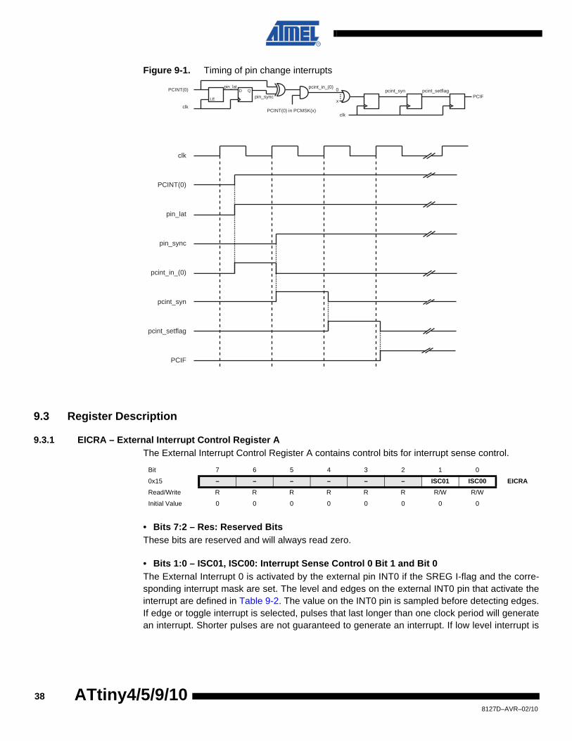
Figure 9-1. Timing of pin change interrupts
9.3 Register Description
9.3.1 EICRA – External Interrupt Control Register AThe External Interrupt Control Register A contains control bits for interrupt sense control.
• Bits 7:2 – Res: Reserved BitsThese bits are reserved and will always read zero.
• Bits 1:0 – ISC01, ISC00: Interrupt Sense Control 0 Bit 1 and Bit 0The External Interrupt 0 is activated by the external pin INT0 if the SREG I-flag and the corre-sponding interrupt mask are set. The level and edges on the external INT0 pin that activate theinterrupt are defined in Table 9-2. The value on the INT0 pin is sampled before detecting edges.If edge or toggle interrupt is selected, pulses that last longer than one clock period will generatean interrupt. Shorter pulses are not guaranteed to generate an interrupt. If low level interrupt is
clk
PCINT(0)
pin_lat
pin_sync
pcint_in_(0)
pcint_syn
pcint_setflag
PCIF
PCINT(0)
pin_syncpcint_syn
pin_latD Q
LE
pcint_setflagPCIF
clk
clkPCINT(0) in PCMSK(x)
pcint_in_(0) 0
x
Bit 7 6 5 4 3 2 1 0
0x15 – – – – – – ISC01 ISC00 EICRA
Read/Write R R R R R R R/W R/W
Initial Value 0 0 0 0 0 0 0 0
388127D–AVR–02/10
ATtiny4/5/9/10

ATtiny4/5/9/10
selected, the low level must be held until the completion of the currently executing instruction togenerate an interrupt.
9.3.2 EIMSK – External Interrupt Mask Register
• Bits 7:1 – Res: Reserved BitsThese bits are reserved and will always read zero.
• Bit 0 – INT0: External Interrupt Request 0 EnableWhen the INT0 bit is set (one) and the I-bit in the Status Register (SREG) is set (one), the exter-nal pin interrupt is enabled. The Interrupt Sense Control bits (ISC01 and ISC00) in the ExternalInterrupt Control Register A (EICRA) define whether the external interrupt is activated on risingand/or falling edge of the INT0 pin or level sensed. Activity on the pin will cause an interruptrequest even if INT0 is configured as an output. The corresponding interrupt of External InterruptRequest 0 is executed from the INT0 Interrupt Vector.
9.3.3 EIFR – External Interrupt Flag Register
• Bits 7:1 – Res: Reserved BitsThese bits are reserved and will always read zero.
• Bit 0 – INTF0: External Interrupt Flag 0When an edge or logic change on the INT0 pin triggers an interrupt request, INTF0 becomes set(one). If the I-bit in SREG and the INT0 bit in EIMSK are set (one), the MCU will jump to the cor-responding Interrupt Vector.
The flag is cleared when the interrupt routine is executed. Alternatively, the flag can be clearedby writing a logical one to it.
This flag is constantly zero when INT0 is configured as a level interrupt.
Table 9-2. Interrupt 0 Sense Control
ISC01 ISC00 Description
0 0 The low level of INT0 generates an interrupt request.
0 1 Any logical change on INT0 generates an interrupt request.
1 0 The falling edge of INT0 generates an interrupt request.
1 1 The rising edge of INT0 generates an interrupt request.
Bit 7 6 5 4 3 2 1 0
0x13 – – – – – – – INTO EIMSK
Read/Write R R R R R R R R/W
Initial Value 0 0 0 0 0 0 0 0
Bit 7 6 5 4 3 2 1 0
0x14 – – – – – – – INTF0 EIFR
Read/Write R R R R R R R R/W
Initial Value 0 0 0 0 0 0 0 0
398127D–AVR–02/10

9.3.4 PCICR – Pin Change Interrupt Control Register
• Bits 7:1 – Res: Reserved BitsThese bits are reserved and will always read zero.
• Bit 0 – PCIE0: Pin Change Interrupt Enable 0When the PCIE0 bit is set (one) and the I-bit in the Status Register (SREG) is set (one), pinchange interrupt 0 is enabled. Any change on any enabled PCINT3..0 pin will cause an interrupt.The corresponding interrupt of Pin Change Interrupt Request is executed from the PCI0 Inter-rupt Vector. PCINT3..0 pins are enabled individually by the PCMSK Register.
9.3.5 PCIFR – Pin Change Interrupt Flag Register
• Bits 7:1 – Res: Reserved BitsThese bits are reserved and will always read zero.
• Bit 0 – PCIF0: Pin Change Interrupt Flag 0When a logic change on any PCINT3..0 pin triggers an interrupt request, PCIF0 becomes set(one). If the I-bit in SREG and the PCIE0 bit in PCICR are set (one), the MCU will jump to thecorresponding Interrupt Vector. The flag is cleared when the interrupt routine is executed. Alter-natively, the flag can be cleared by writing a logical one to it.
9.3.6 PCMSK – Pin Change Mask Register
• Bits 7:4 – Res: Reserved BitsThese bits are reserved and will always read zero.
• Bits 3:0 – PCINT3..0: Pin Change Enable Mask 3..0Each PCINT3..0 bit selects whether pin change interrupt is enabled on the corresponding I/Opin. If PCINT3..0 is set and the PCIE0 bit in PCICR is set, pin change interrupt is enabled on thecorresponding I/O pin. If PCINT3..0 is cleared, pin change interrupt on the corresponding I/O pinis disabled.
Bit 7 6 5 4 3 2 1 0
0x12 – – – – – – – PCIE0 PCICR
Read/Write R R R R R R R R/W
Initial Value 0 0 0 0 0 0 0 0
Bit 7 6 5 4 3 2 1 0
0x11 – – – – – – – PCIF0 PCIFR
Read/Write R R R R R R R R/W
Initial Value 0 0 0 0 0 0 0 0
Bit 7 6 5 4 3 2 1 0
0x10 – – – – PCINT3 PCINT2 PCINT1 PCINT0 PCMSK
Read/Write R R R R R/W R/W R/W R/W
Initial Value 0 0 0 0 0 0 0 0
408127D–AVR–02/10
ATtiny4/5/9/10

ATtiny4/5/9/10
10. I/O Ports
10.1 OverviewAll AVR ports have true Read-Modify-Write functionality when used as general digital I/O ports.This means that the direction of one port pin can be changed without unintentionally changingthe direction of any other pin with the SBI and CBI instructions. The same applies when chang-ing drive value (if configured as output) or enabling/disabling of pull-up resistors. Each outputbuffer has symmetrical drive characteristics with both high sink and source capability. The pindriver is strong enough to drive LED displays directly. All port pins have individually selectablepull-up resistors with a supply-voltage invariant resistance. All I/O pins have protection diodes toboth VCC and Ground as indicated in Figure 10-1 on page 41. See “Electrical Characteristics” onpage 117 for a complete list of parameters.
Figure 10-1. I/O Pin Equivalent Schematic
All registers and bit references in this section are written in general form. A lower case “x” repre-sents the numbering letter for the port, and a lower case “n” represents the bit number. However,when using the register or bit defines in a program, the precise form must be used. For example,PORTB3 for bit no. 3 in Port B, here documented generally as PORTxn. The physical I/O Regis-ters and bit locations are listed in “Register Description” on page 51.
Four I/O memory address locations are allocated for each port, one each for the Data Register –PORTx, Data Direction Register – DDRx, Pull-up Enable Register – PUEx, and the Port InputPins – PINx. The Port Input Pins I/O location is read only, while the Data Register, the DataDirection Register, and the Pull-up Enable Register are read/write. However, writing a logic oneto a bit in the PINx Register, will result in a toggle in the corresponding bit in the Data Register.
Using the I/O port as General Digital I/O is described in “Ports as General Digital I/O” on page42. Most port pins are multiplexed with alternate functions for the peripheral features on thedevice. How each alternate function interferes with the port pin is described in “Alternate PortFunctions” on page 46. Refer to the individual module sections for a full description of the alter-nate functions.
Note that enabling the alternate function of some of the port pins does not affect the use of theother pins in the port as general digital I/O.
Cpin
Logic
Rpu
See Figure"General Digital I/O" for
Details
Pxn
418127D–AVR–02/10

10.2 Ports as General Digital I/OThe ports are bi-directional I/O ports with optional internal pull-ups. Figure 10-2 shows a func-tional description of one I/O-port pin, here generically called Pxn.
Figure 10-2. General Digital I/O(1)
Note: 1. WEx, WRx, WPx, WDx, REx, RRx, RPx, and RDx are common to all pins within the same port. clkI/O, and SLEEP are common to all ports.
10.2.1 Configuring the PinEach port pin consists of four register bits: DDxn, PORTxn, PUExn, and PINxn. As shown in“Register Description” on page 51, the DDxn bits are accessed at the DDRx I/O address, thePORTxn bits at the PORTx I/O address, the PUExn bits at the PUEx I/O address, and the PINxnbits at the PINx I/O address.
clk
RPx
RRx
RDx
WDx
WEx
SYNCHRONIZER
WDx: WRITE DDRx
WRx: WRITE PORTxRRx: READ PORTx REGISTERRPx: READ PORTx PIN
clk I/O: I/O CLOCK
RDx: READ DDRx
WEx: WRITE PUExREx: READ PUEx
D
L
Q
Q
REx
RESET
RESET
Q
QD
Q
Q D
CLR
PORTxn
Q
Q D
CLR
DDxn
PINxn
DAT
A B
US
SLEEP
SLEEP: SLEEP CONTROL
Pxn
I/O
WPx
RESET
Q
Q D
CLR
PUExn
0
1
WRx
WPx: WRITE PINx REGISTER
428127D–AVR–02/10
ATtiny4/5/9/10

ATtiny4/5/9/10
The DDxn bit in the DDRx Register selects the direction of this pin. If DDxn is written logic one,Pxn is configured as an output pin. If DDxn is written logic zero, Pxn is configured as an inputpin.
If PORTxn is written logic one when the pin is configured as an output pin, the port pin is drivenhigh (one). If PORTxn is written logic zero when the pin is configured as an output pin, the portpin is driven low (zero).
The pull-up resistor is activated, if the PUExn is written logic one. To switch the pull-up resistoroff, PUExn has to be written logic zero.
Table 10-1 summarizes the control signals for the pin value.
Port pins are tri-stated when a reset condition becomes active, even when no clocks arerunning.
10.2.2 Toggling the PinWriting a logic one to PINxn toggles the value of PORTxn, independent on the value of DDRxn.Note that the SBI instruction can be used to toggle one single bit in a port.
10.2.3 Break-Before-Make SwitchingIn Break-Before-Make mode, switching the DDRxn bit from input to output introduces an imme-diate tri-state period lasting one system clock cycle, as indicated in Figure 10-3. For example, ifthe system clock is 4 MHz and the DDRxn is written to make an output, an immediate tri-stateperiod of 250 ns is introduced before the value of PORTxn is seen on the port pin.
To avoid glitches it is recommended that the maximum DDRxn toggle frequency is two systemclock cycles. The Break-Before-Make mode applies to the entire port and it is activated by theBBMx bit. For more details, see “PORTCR – Port Control Register” on page 51.
When switching the DDRxn bit from output to input no immediate tri-state period is introduced.
Table 10-1. Port Pin Configurations
DDxn PORTxn PUExn I/O Pull-up Comment
0 X 0 Input No Tri-state (hi-Z)
0 X 1 Input Yes Sources current if pulled low externally
1 0 0 Output No Output low (sink)
1 0 1 Output Yes
NOT RECOMMENDED.Output low (sink) and internal pull-up active. Sources current through the internal pull-up resistor and consumes power constantly
1 1 0 Output No Output high (source)
1 1 1 Output Yes Output high (source) and internal pull-up active
438127D–AVR–02/10

Figure 10-3. Switching Between Input and Output in Break-Before-Make-Mode
10.2.4 Reading the Pin ValueIndependent of the setting of Data Direction bit DDxn, the port pin can be read through thePINxn Register bit. As shown in Figure 10-2 on page 42, the PINxn Register bit and the preced-ing latch constitute a synchronizer. This is needed to avoid metastability if the physical pinchanges value near the edge of the internal clock, but it also introduces a delay. Figure 10-4shows a timing diagram of the synchronization when reading an externally applied pin value.The maximum and minimum propagation delays are denoted tpd,max and tpd,min respectively.
Figure 10-4. Synchronization when Reading an Externally Applied Pin value
Consider the clock period starting shortly after the first falling edge of the system clock. The latchis closed when the clock is low, and goes transparent when the clock is high, as indicated by theshaded region of the “SYNC LATCH” signal. The signal value is latched when the system clockgoes low. It is clocked into the PINxn Register at the succeeding positive clock edge. As indi-cated by the two arrows tpd,max and tpd,min, a single signal transition on the pin will be delayedbetween ½ and 1½ system clock period depending upon the time of assertion.
out DDRx, r16 nop
0x02 0x01
SYSTEM CLK
INSTRUCTIONS
DDRx
intermediate tri-state cycle
out DDRx, r17
0x55PORTx
0x01
intermediate tri-state cycle
Px0
Px1
tri-state
tri-statetri-state
0x01r17
0x02r16
XXX in r17, PINx
0x00 0xFF
INSTRUCTIONS
SYNC LATCH
PINxn
r17
XXX
SYSTEM CLK
tpd, max
tpd, min
448127D–AVR–02/10
ATtiny4/5/9/10

ATtiny4/5/9/10
When reading back a software assigned pin value, a nop instruction must be inserted as indi-cated in Figure 10-5 on page 45. The out instruction sets the “SYNC LATCH” signal at thepositive edge of the clock. In this case, the delay tpd through the synchronizer is one systemclock period.
Figure 10-5. Synchronization when Reading a Software Assigned Pin Value
10.2.5 Digital Input Enable and Sleep ModesAs shown in Figure 10-2 on page 42, the digital input signal can be clamped to ground at theinput of the schmitt-trigger. The signal denoted SLEEP in the figure, is set by the MCU SleepController in Power-down and Standby modes to avoid high power consumption if some inputsignals are left floating, or have an analog signal level close to VCC/2.
SLEEP is overridden for port pins enabled as external interrupt pins. If the external interruptrequest is not enabled, SLEEP is active also for these pins. SLEEP is also overridden by variousother alternate functions as described in “Alternate Port Functions” on page 46.
If a logic high level (“one”) is present on an asynchronous external interrupt pin configured as“Interrupt on Rising Edge, Falling Edge, or Any Logic Change on Pin” while the external interruptis not enabled, the corresponding External Interrupt Flag will be set when resuming from theabove mentioned Sleep mode, as the clamping in these sleep mode produces the requestedlogic change.
10.2.6 Unconnected PinsIf some pins are unused, it is recommended to ensure that these pins have a defined level. Eventhough most of the digital inputs are disabled in the deep sleep modes as described above, float-ing inputs should be avoided to reduce current consumption in all other modes where the digitalinputs are enabled (Reset, Active mode and Idle mode).
The simplest method to ensure a defined level of an unused pin, is to enable the internal pull-up.In this case, the pull-up will be disabled during reset. If low power consumption during reset isimportant, it is recommended to use an external pull-up or pulldown. Connecting unused pinsdirectly to VCC or GND is not recommended, since this may cause excessive currents if the pin isaccidentally configured as an output.
out PORTx, r16 nop in r17, PINx
0xFF
0x00 0xFF
SYSTEM CLK
r16
INSTRUCTIONS
SYNC LATCH
PINxn
r17tpd
458127D–AVR–02/10

10.2.7 Program ExampleThe following code example shows how to set port B pin 0 high, pin 1 low, and define the portpins from 2 to 3 as input with a pull-up assigned to port pin 2. The resulting pin values are readback again, but as previously discussed, a nop instruction is included to be able to read back thevalue recently assigned to some of the pins.
Note: See “Code Examples” on page 5.
10.3 Alternate Port FunctionsMost port pins have alternate functions in addition to being general digital I/Os. In Figure 10-6below is shown how the port pin control signals from the simplified Figure 10-2 on page 42 canbe overridden by alternate functions.
Assembly Code Example
...
; Define pull-ups and set outputs high
; Define directions for port pins
ldi r16,(1<<PUEB2)
ldi r17,(1<<PB0)
ldi r18,(1<<DDB1)|(1<<DDB0)
out PUEB,r16
out PORTB,r17
out DDRB,r18
; Insert nop for synchronization
nop
; Read port pins
in r16,PINB
...
468127D–AVR–02/10
ATtiny4/5/9/10

ATtiny4/5/9/10
Figure 10-6. Alternate Port Functions(1)
Note: 1. WEx, WRx, WPx, WDx, REx, RRx, RPx, and RDx are common to all pins within the same port. clkI/O, and SLEEP are common to all ports. All other signals are unique for each pin.
The illustration in the figure above serves as a generic description applicable to all port pins inthe AVR microcontroller family. Some overriding signals may not be present in all port pins.
clk
RPx
RRxWRx
RDx
WDx
SYNCHRONIZER
WDx: WRITE DDRx
WRx: WRITE PORTxRRx: READ PORTx REGISTER
RPx: READ PORTx PIN
REx: READ PUExWEx: WRITE PUEx
clk I/O: I/O CLOCK
RDx: READ DDRx
D
L
Q
Q
SET
CLR
0
1
0
1
0
1
DIxn
AIOxn
DIEOExn
PVOVxn
PVOExn
DDOVxn
DDOExn
PUOExn
PUOVxn
PUOExn: Pxn PULL-UP OVERRIDE ENABLEPUOVxn: Pxn PULL-UP OVERRIDE VALUEDDOExn: Pxn DATA DIRECTION OVERRIDE ENABLEDDOVxn: Pxn DATA DIRECTION OVERRIDE VALUEPVOExn: Pxn PORT VALUE OVERRIDE ENABLEPVOVxn: Pxn PORT VALUE OVERRIDE VALUE
DIxn: DIGITAL INPUT PIN n ON PORTxAIOxn: ANALOG INPUT/OUTPUT PIN n ON PORTx
RESET
RESET
Q
Q D
CLR
Q
Q D
CLR
Q
QD
CLR
PINxn
PORTxn
DDxn
DAT
A B
US
0
1DIEOVxn
SLEEP
DIEOExn: Pxn DIGITAL INPUT-ENABLE OVERRIDE ENABLEDIEOVxn: Pxn DIGITAL INPUT-ENABLE OVERRIDE VALUESLEEP: SLEEP CONTROL
Pxn
I/O
0
1
PTOExn
PTOExn: Pxn, PORT TOGGLE OVERRIDE ENABLE
WPx: WRITE PINx
WPx
WEx
REx
RESET
Q
Q D
CLR
PUExn
478127D–AVR–02/10

Table 10-2 on page 48 summarizes the function of the overriding signals. The pin and portindexes from Figure 10-6 on page 47 are not shown in the succeeding tables. The overridingsignals are generated internally in the modules having the alternate function.
The following subsections shortly describe the alternate functions for each port, and relate theoverriding signals to the alternate function. Refer to the alternate function description for furtherdetails.
Table 10-2. Generic Description of Overriding Signals for Alternate Functions
Signal Name Full Name Description
PUOEPull-up Override Enable
If this signal is set, the pull-up enable is controlled by the PUOV signal. If this signal is cleared, the pull-up is enabled when PUExn = 0b1.
PUOVPull-up Override Value
If PUOE is set, the pull-up is enabled/disabled when PUOV is set/cleared, regardless of the setting of the PUExn Register bit.
DDOEData Direction Override Enable
If this signal is set, the Output Driver Enable is controlled by the DDOV signal. If this signal is cleared, the Output driver is enabled by the DDxn Register bit.
DDOVData Direction Override Value
If DDOE is set, the Output Driver is enabled/disabled when DDOV is set/cleared, regardless of the setting of the DDxn Register bit.
PVOEPort Value Override Enable
If this signal is set and the Output Driver is enabled, the port value is controlled by the PVOV signal. If PVOE is cleared, and the Output Driver is enabled, the port Value is controlled by the PORTxn Register bit.
PVOVPort Value Override Value
If PVOE is set, the port value is set to PVOV, regardless of the setting of the PORTxn Register bit.
PTOEPort Toggle Override Enable
If PTOE is set, the PORTxn Register bit is inverted.
DIEOEDigital Input Enable Override Enable
If this bit is set, the Digital Input Enable is controlled by the DIEOV signal. If this signal is cleared, the Digital Input Enable is determined by MCU state (Normal mode, sleep mode).
DIEOVDigital Input Enable Override Value
If DIEOE is set, the Digital Input is enabled/disabled when DIEOV is set/cleared, regardless of the MCU state (Normal mode, sleep mode).
DI Digital Input
This is the Digital Input to alternate functions. In the figure, the signal is connected to the output of the schmitt-trigger but before the synchronizer. Unless the Digital Input is used as a clock source, the module with the alternate function will use its own synchronizer.
AIOAnalog Input/Output
This is the Analog Input/Output to/from alternate functions. The signal is connected directly to the pad, and can be used bi-directionally.
488127D–AVR–02/10
ATtiny4/5/9/10

ATtiny4/5/9/10
10.3.1 Alternate Functions of Port B The Port B pins with alternate function are shown in Table 10-3 on page 49.
• Port B, Bit 0 – ADC0/AIN0/OC0A/PCINT0/TPIDATA
• ADC0: Analog to Digital Converter, Channel 0 (ATtiny5/10, only)
• AIN0: Analog Comparator Positive Input. Configure the port pin as input with the internal pull-up switched off to avoid the digital port function from interfering with the function of the Analog Comparator.
• OC0A, Output Compare Match output: The PB0 pin can serve as an external output for the Timer/Counter0 Compare Match A. The pin has to be configured as an output (DDB0 set (one)) to serve this function. This is also the output pin for the PWM mode timer function.
• PCINT0: Pin Change Interrupt source 0. The PB0 pin can serve as an external interrupt source for pin change interrupt 0.
• TPIDATA: Serial Programming Data.
• Port B, Bit 1 – ADC1/AIN1/CLKI/ICP0/OC0B/PCINT1/TPICLK
• ADC1: Analog to Digital Converter, Channel 1 (ATtiny5/10, only)
• AIN1: Analog Comparator Negative Input. Configure the port pin as input with the internal pull-up switched off to avoid the digital port function from interfering with the function of the Analog Comparator.
• CLKI: External Clock.
• ICP0: Input Capture Pin. The PB1 pin can act as an Input Capture pin for Timer/Counter0.
Table 10-3. Port B Pins Alternate Functions
Port Pin Alternate Function
PB0
ADC0: ADC Input Channel 0
AIN0: Analog Comparator, Positive Input
OC0A: Timer/Counter0 Compare Match A OutputPCINT0: Pin Change Interrupt 0, Source 0
TPIDATA:Serial Programming Data
PB1
ADC1: ADC Input Channel 1
AIN1: Analog Comparator, Negative Input
CLKI: External ClockICP0: Timer/Counter0 Input Capture Input
OC0B: Timer/Counter0 Compare Match B Output
PCINT1:Pin Change Interrupt 0, Source 1TPICLK: Serial Programming Clock
PB2
ADC2: ADC Input Channel 2CLKO: System Clock Output
INT0: External Interrupt 0 Source
PCINT2: Pin Change Interrupt 0, Source 2T0: Timer/Counter0 Clock Source
PB3ADC3: ADC Input Channel 3PCINT3: Pin Change Interrupt 0, Source 3
RESET: Reset Pin
498127D–AVR–02/10

• OC0B: Output Compare Match output: The PB1 pin can serve as an external output for the Timer/Counter0 Compare Match B. The PB1 pin has to be configured as an output (DDB1 set (one)) to serve this function. The OC0B pin is also the output pin for the PWM mode timer function.
• PCINT1: Pin Change Interrupt source 1. The PB1 pin can serve as an external interrupt source for pin change interrupt 0.
• TPICLK: Serial Programming Clock.
• Port B, Bit 2 – ADC2/CLKO/INT0/PCINT2/T0
• ADC2: Analog to Digital Converter, Channel 2 (ATtiny5/10, only)
• CLKO: System Clock Output. The system clock can be output on pin PB2. The system clock will be output if CKOUT bit is programmed, regardless of the PORTB2 and DDB2 settings.
• INT0: External Interrupt Request 0
• PCINT2: Pin Change Interrupt source 2. The PB2 pin can serve as an external interrupt source for pin change interrupt 0.
• T0: Timer/Counter0 counter source.
• Port B, Bit 3 – ADC3/PCINT3/RESET
• ADC3: Analog to Digital Converter, Channel 3 (ATtiny5/10, only)
• PCINT3: Pin Change Interrupt source 3. The PB3 pin can serve as an external interrupt source for pin change interrupt 0.
• RESET:
Table 10-4 and Table 10-5 on page 51 relate the alternate functions of Port B to the overridingsignals shown in Figure 10-6 on page 47.
Table 10-4. Overriding Signals for Alternate Functions in PB3..PB2
Notes: 1. RSTDISBL is 1 when the configuration bit is “0” (Programmed).
2. CKOUT is 1 when the configuration bit is “0” (Programmed).
SignalName PB3/ADC3/RESET/PCINT3 PB2/ADC2/INT0/T0/CLKO/PCINT2
PUOE RSTDISBL(1) CKOUT(2)
PUOV 1 0
DDOE RSTDISBL(1) CKOUT(2)
DDOV 0 1
PVOE 0 CKOUT(2)
PVOV 0 (system clock)
PTOE 0 0
DIEOERSTDISBL(1) + (PCINT3 • PCIE0) + ADC3D
(PCINT2 • PCIE0) + ADC2D + INT0
DIEOV RSTDISBL • PCINT3 • PCIE0 (PCINT2 • PCIE0) + INT0
DI PCINT3 Input INT0/T0/PCINT2 Input
AIO ADC3 Input ADC2 Input
508127D–AVR–02/10
ATtiny4/5/9/10

ATtiny4/5/9/10
Notes: 1. EXT_CLOCK is 1 when external clock is selected as main clock.
10.4 Register Description
10.4.1 PORTCR – Port Control Register
• Bits 7:2, 0 – ReservedThese bits are reserved and will always read zero.
• Bit 1 – BBMB: Break-Before-Make Mode EnableWhen this bit is set the Break-Before-Make mode is activated for the entire Port B. The interme-diate tri-state cycle is then inserted when writing DDRxn to make an output. For furtherinformation, see “Break-Before-Make Switching” on page 43.
10.4.2 PUEB – Port B Pull-up Enable Control Register
Table 10-5. Overriding Signals for Alternate Functions in PB1..PB0
SignalName PB1/ADC1/AIN1/OC0B/CLKI/ICP0/PCINT1 PB0/ADC0/AIN0/OC0A/PCINT0
PUOE EXT_CLOCK(1) 0
PUOV 0 0
DDOE EXT_CLOCK(1) 0
DDOV 0 0
PVOE EXT_CLOCK(1) + OC0B Enable OC0A Enable
PVOV EXT_CLOCK(1) • OC0B OC0A
PTOE 0 0
DIEOEEXT_CLOCK(1) + (PCINT1 • PCIE0) + ADC1D
(PCINT0 • PCIE0) + ADC0D
DIEOV(EXT_CLOCK(1) • PWR_DOWN) + (EXT_CLOCK(1) • PCINT1 • PCIE0)
PCINT0 • PCIE0
DI CLOCK/ICP0/PCINT1 Input PCINT0 Input
AIO ADC1/Analog Comparator Negative Input ADC0/Analog Comparator Positive Input
Bit 7 6 5 4 3 2 1 0
0x03 – – – – – – BBMB – PORTCR
Read/Write R R R R R R R/W R
Initial Value 0 0 0 0 0 0 0 0
Bit 7 6 5 4 3 2 1 0
0x03 – – – – PUEB3 PUEB2 PUEB1 PUEB0 PUEB
Read/Write R R R R R/W R/W R/W R/W
Initial Value 0 0 0 0 0 0 0 0
518127D–AVR–02/10

10.4.3 PORTB – Port B Data Register
10.4.4 DDRB – Port B Data Direction Register
10.4.5 PINB – Port B Input Pins
Bit 7 6 5 4 3 2 1 0
0x02 – – – – PORTB3 PORTB2 PORTB1 PORTB0 PORTB
Read/Write R R R R R/W R/W R/W R/W
Initial Value 0 0 0 0 0 0 0 0
Bit 7 6 5 4 3 2 1 0
0x01 – – – – DDB3 DDB2 DDB1 DDB0 DDRB
Read/Write R R R R R/W R/W R/W R/W
Initial Value 0 0 0 0 0 0 0 0
Bit 7 6 5 4 3 2 1 0
0x00 – – – – PINB3 PINB2 PINB1 PINB0 PINB
Read/Write R R R R R/W R/W R/W R/W
Initial Value 0 0 0 0 N/A N/A N/A N/A
528127D–AVR–02/10
ATtiny4/5/9/10

ATtiny4/5/9/10
11. 16-bit Timer/Counter0
11.1 Features• True 16-bit Design, Including 16-bit PWM• Two Independent Output Compare Units• Double Buffered Output Compare Registers• One Input Capture Unit• Input Capture Noise Canceler• Clear Timer on Compare Match (Auto Reload)• Glitch-free, Phase Correct Pulse Width Modulator (PWM)• Variable PWM Period• Frequency Generator• External Event Counter• Four independent interrupt Sources (TOV0, OCF0A, OCF0B, and ICF0)
11.2 OverviewThe 16-bit Timer/Counter unit allows accurate program execution timing (event management),wave generation, and signal timing measurement.
Figure 11-1. 16-bit Timer/Counter Block Diagram
Clock Select
Timer/Counter
DAT
A B
US
OCRnA
OCRnB
ICRn
=
=
TCNTn
WaveformGeneration
WaveformGeneration
OCnA
OCnB
NoiseCanceler
ICPn
=
FixedTOP
Values
EdgeDetector
Control Logic
= 0
TOP BOTTOM
Count
Clear
Direction
TOVn(Int.Req.)
OCnA(Int.Req.)
OCnB(Int.Req.)
ICFn (Int.Req.)
TCCRnA TCCRnB
( From AnalogComparator Ouput )
TnEdge
Detector
( From Prescaler )
clkTn
538127D–AVR–02/10

A simplified block diagram of the 16-bit Timer/Counter is shown in Figure 11-1 on page 53. Foractual placement of I/O pins, refer to “Pinout of ATtiny4/5/9/10” on page 2. CPU accessible I/ORegisters, including I/O bits and I/O pins, are shown in bold. The device-specific I/O Registerand bit locations are listed in the “Register Description” on page 74.
Most register and bit references in this section are written in general form. A lower case “n”replaces the Timer/Counter number, and a lower case “x” replaces the Output Compare unitchannel. However, when using the register or bit defines in a program, the precise form must beused, i.e., TCNT0 for accessing Timer/Counter0 counter value and so on.
11.2.1 RegistersThe Timer/Counter (TCNT0), Output Compare Registers (OCR0A/B), and Input Capture Regis-ter (ICR0) are all 16-bit registers. Special procedures must be followed when accessing the 16-bit registers. These procedures are described in the section “Accessing 16-bit Registers” onpage 72. The Timer/Counter Control Registers (TCCR0A/B) are 8-bit registers and have no CPUaccess restrictions. Interrupt requests (abbreviated to Int.Req. in the figure) signals are all visiblein the Timer Interrupt Flag Register (TIFR). All interrupts are individually masked with the TimerInterrupt Mask Register (TIMSK). TIFR and TIMSK are not shown in the figure.
The Timer/Counter can be clocked internally, via the prescaler, or by an external clock source onthe T0 pin. The Clock Select logic block controls which clock source and edge the Timer/Counteruses to increment (or decrement) its value. The Timer/Counter is inactive when no clock sourceis selected. The output from the Clock Select logic is referred to as the timer clock (clkT0).
The double buffered Output Compare Registers (OCR0A/B) are compared with the Timer/Coun-ter value at all time. The result of the compare can be used by the Waveform Generator togenerate a PWM or variable frequency output on the Output Compare pin (OC0A/B). See “Out-put Compare Units” on page 60. The compare match event will also set the Compare MatchFlag (OCF0A/B) which can be used to generate an Output Compare interrupt request.
The Input Capture Register can capture the Timer/Counter value at a given external (edge trig-gered) event on either the Input Capture pin (ICP0) or on the Analog Comparator pins (See“Analog Comparator” on page 82). The Input Capture unit includes a digital filtering unit (NoiseCanceler) for reducing the chance of capturing noise spikes.
The TOP value, or maximum Timer/Counter value, can in some modes of operation be definedby either the OCR0A Register, the ICR0 Register, or by a set of fixed values. When usingOCR0A as TOP value in a PWM mode, the OCR0A Register can not be used for generating aPWM output. However, the TOP value will in this case be double buffered allowing the TOPvalue to be changed in run time. If a fixed TOP value is required, the ICR0 Register can be usedas an alternative, freeing the OCR0A to be used as PWM output.
11.2.2 DefinitionsThe following definitions are used extensively throughout the section:
Table 11-1. Definitions
Constant Description
BOTTOM The counter reaches BOTTOM when it becomes 0x00
MAX The counter reaches its MAXimum when it becomes 0xFF (decimal 255)
TOPThe counter reaches the TOP when it becomes equal to the highest value in the count sequence. The TOP value can be assigned to be the fixed value 0xFF (MAX) or the value stored in the OCR0A Register. The assignment depends on the mode of operation
548127D–AVR–02/10
ATtiny4/5/9/10

ATtiny4/5/9/10
11.3 Clock SourcesThe Timer/Counter can be clocked by an internal or an external clock source. The clock sourceis selected by the Clock Select logic which is controlled by the Clock Select (CS02:0) bitslocated in the Timer/Counter control Register B (TCCR0B). For details on clock sources andprescaler, see section “Prescaler”.
11.3.1 PrescalerThe Timer/Counter can be clocked directly by the system clock (by setting the CS2:0 = 1). Thisprovides the fastest operation, with a maximum Timer/Counter clock frequency equal to systemclock frequency (fCLK_I/O). Alternatively, one of four taps from the prescaler can be used as aclock source.
See Figure 11-2 for an illustration of the prescaler unit.
Figure 11-2. Prescaler for Timer/Counter0
Note: 1. The synchronization logic on the input pins (T0) is shown in Figure 11-3 on page 56.
The prescaled clock has a frequency of fCLK_I/O/8, fCLK_I/O/64, fCLK_I/O/256, or fCLK_I/O/1024. SeeTable 11-6 on page 77 for details.
11.3.1.1 Prescaler ResetThe prescaler is free running, i.e., operates independently of the Clock Select logic of theTimer/CounterCounter, and it is shared by the Timer/Counter Tn. Since the prescaler is notaffected by the Timer/Counter’s clock select, the state of the prescaler will have implications forsituations where a prescaled clock is used. One example of prescaling artifacts occurs when thetimer is enabled and clocked by the prescaler (CS2:0 = 2, 3, 4, or 5). The number of system
PSR10
Clear
clkT0
T0
clkI/O
Synchronization
558127D–AVR–02/10

clock cycles from when the timer is enabled to the first count occurs can be from 1 to N+1 sys-tem clock cycles, where N equals the prescaler divisor (8, 64, 256, or 1024).
It is possible to use the Prescaler Reset for synchronizing the Timer/Counter to programexecution.
11.3.2 External Clock SourceAn external clock source applied to the T0 pin can be used as Timer/Counter clock (clkTn). TheTn pin is sampled once every system clock cycle by the pin synchronization logic. The synchro-nized (sampled) signal is then passed through the edge detector. Figure 11-3 on page 56 showsa functional equivalent block diagram of the T0 synchronization and edge detector logic. Theregisters are clocked at the positive edge of the internal system clock (clkI/O). The latch is trans-parent in the high period of the internal system clock.
The edge detector generates one clkT0 pulse for each positive (CS2:0 = 7) or negative (CS2:0 =6) edge it detects.
Figure 11-3. T0 Pin Sampling
The synchronization and edge detector logic introduces a delay of 2.5 to 3.5 system clock cyclesfrom an edge has been applied to the T0 pin to the counter is updated.
Enabling and disabling of the clock input must be done when T0 has been stable for at least onesystem clock cycle, otherwise it is a risk that a false Timer/Counter clock pulse is generated.
Each half period of the external clock applied must be longer than one system clock cycle toensure correct sampling. The external clock must be guaranteed to have less than half the sys-tem clock frequency (fExtClk < fclk_I/O/2) given a 50/50% duty cycle. Since the edge detector usessampling, the maximum frequency of an external clock it can detect is half the sampling fre-quency (Nyquist sampling theorem). However, due to variation of the system clock frequencyand duty cycle caused by oscillator source (crystal, resonator, and capacitors) tolerances, it isrecommended that maximum frequency of an external clock source is less than fclk_I/O/2.5.
An external clock source can not be prescaled.
11.4 Counter UnitThe main part of the 16-bit Timer/Counter is the programmable 16-bit bi-directional counter unit.Figure 11-4 on page 57 shows a block diagram of the counter and its surroundings.
Tn_sync(To ClockSelect Logic)
Edge DetectorSynchronization
D QD Q
LE
D QTn
clkI/O
568127D–AVR–02/10
ATtiny4/5/9/10

ATtiny4/5/9/10
Figure 11-4. Counter Unit Block Diagram
Signal description (internal signals):
Count Increment or decrement TCNT0 by 1.Direction Select between increment and decrement.Clear Clear TCNT0 (set all bits to zero).clkT0 Timer/Counter clock.TOP Signalize that TCNT0 has reached maximum value.BOTTOM Signalize that TCNT0 has reached minimum value (zero).
The 16-bit counter is mapped into two 8-bit I/O memory locations: Counter High (TCNT0H) con-taining the upper eight bits of the counter, and Counter Low (TCNT0L) containing the lower eightbits. The TCNT0H Register can only be indirectly accessed by the CPU. When the CPU does anaccess to the TCNT0H I/O location, the CPU accesses the high byte temporary register (TEMP).The temporary register is updated with the TCNT0H value when the TCNT0L is read, andTCNT0H is updated with the temporary register value when TCNT0L is written. This allows theCPU to read or write the entire 16-bit counter value within one clock cycle via the 8-bit data bus.It is important to notice that there are special cases of writing to the TCNT0 Register when thecounter is counting that will give unpredictable results. The special cases are described in thesections where they are of importance.
Depending on the mode of operation used, the counter is cleared, incremented, or decrementedat each timer clock (clkT0). The clkT0 can be generated from an external or internal clock source,selected by the Clock Select bits (CS02:0). When no clock source is selected (CS02:0 = 0) thetimer is stopped. However, the TCNT0 value can be accessed by the CPU, independent ofwhether clkT0 is present or not. A CPU write overrides (has priority over) all counter clear orcount operations.
The counting sequence is determined by the setting of the Waveform Generation mode bits(WGM03:0) located in the Timer/Counter Control Registers A and B (TCCR0A and TCCR0B).There are close connections between how the counter behaves (counts) and how waveformsare generated on the Output Compare outputs OC0x. For more details about advanced countingsequences and waveform generation, see “Modes of Operation” on page 63.
The Timer/Counter Overflow Flag (TOV0) is set according to the mode of operation selected bythe WGM03:0 bits. TOV0 can be used for generating a CPU interrupt.
TEMP (8-bit)
DATA BUS (8-bit)
TCNTn (16-bit Counter)
TCNTnH (8-bit) TCNTnL (8-bit)Control Logic
Count
Clear
Direction
TOVn(Int.Req.)
Clock Select
TOP BOTTOM
TnEdge
Detector
( From Prescaler )
clkTn
578127D–AVR–02/10

11.5 Input Capture UnitThe Timer/Counter incorporates an Input Capture unit that can capture external events and givethem a time-stamp indicating time of occurrence. The external signal indicating an event, or mul-tiple events, can be applied via the ICP0 pin. The time-stamps can then be used to calculatefrequency, duty-cycle, and other features of the signal applied. Alternatively the time-stamps canbe used for creating a log of the events.
The Input Capture unit is illustrated by the block diagram shown in Figure 11-5 on page 58. Theelements of the block diagram that are not directly a part of the Input Capture unit are grayshaded. The lower case “n” in register and bit names indicates the Timer/Counter number.
Figure 11-5. Input Capture Unit Block Diagram
When a change of the logic level (an event) occurs on the Input Capture pin (ICP0), alternativelyon the Analog Comparator output (ACO), and this change confirms to the setting of the edgedetector, a capture will be triggered. When a capture is triggered, the 16-bit value of the counter(TCNT0) is written to the Input Capture Register (ICR0). The Input Capture Flag (ICF0) is set atthe same system clock as the TCNT0 value is copied into ICR0 Register. If enabled (ICIE0 = 1),the Input Capture Flag generates an Input Capture interrupt. The ICF0 flag is automaticallycleared when the interrupt is executed. Alternatively the ICF0 flag can be cleared by software bywriting a logical one to its I/O bit location.
Reading the 16-bit value in the Input Capture Register (ICR0) is done by first reading the lowbyte (ICR0L) and then the high byte (ICR0H). When the low byte is read the high byte is copiedinto the high byte temporary register (TEMP). When the CPU reads the ICR0H I/O location it willaccess the TEMP Register.
The ICR0 Register can only be written when using a Waveform Generation mode that utilizesthe ICR0 Register for defining the counter’s TOP value. In these cases the Waveform Genera-
ICFn (Int.Req.)
AnalogComparator
WRITE ICRn (16-bit Register)
ICRnH (8-bit)
NoiseCanceler
ICPn
EdgeDetector
TEMP (8-bit)
DATA BUS (8-bit)
ICRnL (8-bit)
TCNTn (16-bit Counter)
TCNTnH (8-bit) TCNTnL (8-bit)
ACIC* ICNC ICESACO*
588127D–AVR–02/10
ATtiny4/5/9/10

ATtiny4/5/9/10
tion mode (WGM03:0) bits must be set before the TOP value can be written to the ICR0Register. When writing the ICR0 Register the high byte must be written to the ICR0H I/O locationbefore the low byte is written to ICR0L.
For more information on how to access the 16-bit registers refer to “Accessing 16-bit Registers”on page 72.
11.5.1 Input Capture Trigger SourceThe main trigger source for the Input Capture unit is the Input Capture pin (ICP0).Timer/Counter0 can alternatively use the Analog Comparator output as trigger source for theInput Capture unit. The Analog Comparator is selected as trigger source by setting the AnalogComparator Input Capture (ACIC) bit in “ACSR – Analog Comparator Control and Status Regis-ter”. Be aware that changing trigger source can trigger a capture. The Input Capture Flag musttherefore be cleared after the change.
Both the Input Capture pin (ICP0) and the Analog Comparator output (ACO) inputs are sampledusing the same technique as for the T0 pin (Figure 11-3 on page 56). The edge detector is alsoidentical. However, when the noise canceler is enabled, additional logic is inserted before theedge detector, which increases the delay by four system clock cycles. Note that the input of thenoise canceler and edge detector is always enabled unless the Timer/Counter is set in a Wave-form Generation mode that uses ICR0 to define TOP.
An Input Capture can be triggered by software by controlling the port of the ICP0 pin.
11.5.2 Noise CancelerThe noise canceler improves noise immunity by using a simple digital filtering scheme. Thenoise canceler input is monitored over four samples, and all four must be equal for changing theoutput that in turn is used by the edge detector.
The noise canceler is enabled by setting the Input Capture Noise Canceler (ICNC0) bit inTimer/Counter Control Register B (TCCR0B). When enabled the noise canceler introduces addi-tional four system clock cycles of delay from a change applied to the input, to the update of theICR0 Register. The noise canceler uses the system clock and is therefore not affected by theprescaler.
11.5.3 Using the Input Capture UnitThe main challenge when using the Input Capture unit is to assign enough processor capacityfor handling the incoming events. The time between two events is critical. If the processor hasnot read the captured value in the ICR0 Register before the next event occurs, the ICR0 will beoverwritten with a new value. In this case the result of the capture will be incorrect.
When using the Input Capture interrupt, the ICR0 Register should be read as early in the inter-rupt handler routine as possible. Even though the Input Capture interrupt has relatively highpriority, the maximum interrupt response time is dependent on the maximum number of clockcycles it takes to handle any of the other interrupt requests.
Using the Input Capture unit in any mode of operation when the TOP value (resolution) isactively changed during operation, is not recommended.
Measurement of an external signal’s duty cycle requires that the trigger edge is changed aftereach capture. Changing the edge sensing must be done as early as possible after the ICR0Register has been read. After a change of the edge, the Input Capture Flag (ICF0) must be
598127D–AVR–02/10

cleared by software (writing a logical one to the I/O bit location). For measuring frequency only,the clearing of the ICF0 flag is not required (if an interrupt handler is used).
11.6 Output Compare UnitsThe 16-bit comparator continuously compares TCNT0 with the Output Compare Register(OCR0x). If TCNT equals OCR0x the comparator signals a match. A match will set the OutputCompare Flag (OCF0x) at the next timer clock cycle. If enabled (OCIE0x = 1), the Output Com-pare Flag generates an Output Compare interrupt. The OCF0x flag is automatically clearedwhen the interrupt is executed. Alternatively the OCF0x flag can be cleared by software by writ-ing a logical one to its I/O bit location. The Waveform Generator uses the match signal togenerate an output according to operating mode set by the Waveform Generation mode(WGM03:0) bits and Compare Output mode (COM0x1:0) bits. The TOP and BOTTOM signalsare used by the Waveform Generator for handling the special cases of the extreme values insome modes of operation (“Modes of Operation” on page 63).
A special feature of Output Compare unit A allows it to define the Timer/Counter TOP value (i.e.,counter resolution). In addition to the counter resolution, the TOP value defines the period timefor waveforms generated by the Waveform Generator.
Figure 11-6 on page 60 shows a block diagram of the Output Compare unit. The small “n” in theregister and bit names indicates the device number (n = 0 for Timer/Counter 0), and the “x” indi-cates Output Compare unit (A/B). The elements of the block diagram that are not directly a partof the Output Compare unit are gray shaded.
Figure 11-6. Output Compare Unit, Block Diagram
The OCR0x Register is double buffered when using any of the twelve Pulse Width Modulation(PWM) modes. For the Normal and Clear Timer on Compare (CTC) modes of operation, the
OCFnx (Int.Req.)
= (16-bit Comparator )
OCRnx Buffer (16-bit Register)
OCRnxH Buf. (8-bit)
OCnx
TEMP (8-bit)
DATA BUS (8-bit)
OCRnxL Buf. (8-bit)
TCNTn (16-bit Counter)
TCNTnH (8-bit) TCNTnL (8-bit)
COMnx1:0WGMn3:0
OCRnx (16-bit Register)
OCRnxH (8-bit) OCRnxL (8-bit)
Waveform GeneratorTOP
BOTTOM
608127D–AVR–02/10
ATtiny4/5/9/10

ATtiny4/5/9/10
double buffering is disabled. The double buffering synchronizes the update of the OCR0x Com-pare Register to either TOP or BOTTOM of the counting sequence. The synchronizationprevents the occurrence of odd-length, non-symmetrical PWM pulses, thereby making the out-put glitch-free.
The OCR0x Register access may seem complex, but this is not case. When the double bufferingis enabled, the CPU has access to the OCR0x Buffer Register, and if double buffering is dis-abled the CPU will access the OCR0x directly. The content of the OCR0x (Buffer or Compare)Register is only changed by a write operation (the Timer/Counter does not update this registerautomatically as the TCNT0 and ICR0 Register). Therefore OCR0x is not read via the high bytetemporary register (TEMP). However, it is a good practice to read the low byte first as whenaccessing other 16-bit registers. Writing the OCR0x Registers must be done via the TEMP Reg-ister since the compare of all 16 bits is done continuously. The high byte (OCR0xH) has to bewritten first. When the high byte I/O location is written by the CPU, the TEMP Register will beupdated by the value written. Then when the low byte (OCR0xL) is written to the lower eight bits,the high byte will be copied into the upper 8-bits of either the OCR0x buffer or OCR0x CompareRegister in the same system clock cycle.
For more information of how to access the 16-bit registers refer to “Accessing 16-bit Registers”on page 72.
11.6.1 Force Output CompareIn non-PWM Waveform Generation modes, the match output of the comparator can be forced bywriting a one to the Force Output Compare (0x) bit. Forcing compare match will not set theOCF0x flag or reload/clear the timer, but the OC0x pin will be updated as if a real comparematch had occurred (the COM01:0 bits settings define whether the OC0x pin is set, cleared ortoggled).
11.6.2 Compare Match Blocking by TCNT0 WriteAll CPU writes to the TCNT0 Register will block any compare match that occurs in the next timerclock cycle, even when the timer is stopped. This feature allows OCR0x to be initialized to thesame value as TCNT0 without triggering an interrupt when the Timer/Counter clock is enabled.
11.6.3 Using the Output Compare UnitSince writing TCNT0 in any mode of operation will block all compare matches for one timer clockcycle, there are risks involved when changing TCNT0 when using any of the Output Comparechannels, independent of whether the Timer/Counter is running or not. If the value written toTCNT0 equals the OCR0x value, the compare match will be missed, resulting in incorrect wave-form generation. Do not write the TCNT0 equal to TOP in PWM modes with variable TOPvalues. The compare match for the TOP will be ignored and the counter will continue to 0xFFFF.Similarly, do not write the TCNT0 value equal to BOTTOM when the counter is downcounting.
The setup of the OC0x should be performed before setting the Data Direction Register for theport pin to output. The easiest way of setting the OC0x value is to use the Force Output Com-pare (0x) strobe bits in Normal mode. The OC0x Register keeps its value even when changingbetween Waveform Generation modes.
Be aware that the COM0x1:0 bits are not double buffered together with the compare value.Changing the COM0x1:0 bits will take effect immediately.
618127D–AVR–02/10

11.7 Compare Match Output UnitThe Compare Output Mode (COM0x1:0) bits have two functions. The Waveform Generator usesthe COM0x1:0 bits for defining the Output Compare (OC0x) state at the next compare match.Secondly the COM0x1:0 bits control the OC0x pin output source. Figure 11-7 on page 62 showsa simplified schematic of the logic affected by the COM0x1:0 bit setting. The I/O Registers, I/Obits, and I/O pins in the figure are shown in bold. Only the parts of the general I/O port controlregisters (DDR and PORT) that are affected by the COM0x1:0 bits are shown. When referring tothe OC0x state, the reference is for the internal OC0x Register, not the OC0x pin. If a systemreset occur, the OC0x Register is reset to “0”.
Figure 11-7. Compare Match Output Unit, Schematic (non-PWM Mode)
The general I/O port function is overridden by the Output Compare (OC0x) from the WaveformGenerator if either of the COM0x1:0 bits are set. However, the OC0x pin direction (input or out-put) is still controlled by the Data Direction Register (DDR) for the port pin. The Data DirectionRegister bit for the OC0x pin (DDR_OC0x) must be set as output before the OC0x value is visi-ble on the pin. The port override function is generally independent of the Waveform Generationmode, but there are some exceptions. See Table 11-2 on page 75, Table 11-3 on page 75 andTable 11-4 on page 75 for details.
The design of the Output Compare pin logic allows initialization of the OC0x state before the out-put is enabled. Note that some COM0x1:0 bit settings are reserved for certain modes ofoperation. See “Register Description” on page 74
The COM0x1:0 bits have no effect on the Input Capture unit.
PORT
DDR
D Q
D Q
OCnxPinOCnx
D QWaveformGenerator
COMnx1
COMnx0
0
1
DAT
A B
US
FOCnx
clkI/O
628127D–AVR–02/10
ATtiny4/5/9/10

ATtiny4/5/9/10
11.7.1 Compare Output Mode and Waveform GenerationThe Waveform Generator uses the COM0x1:0 bits differently in normal, CTC, and PWM modes.For all modes, setting the COM0x1:0 = 0 tells the Waveform Generator that no action on theOC0x Register is to be performed on the next compare match. For compare output actions in thenon-PWM modes refer to Table 11-2 on page 75. For fast PWM mode refer to Table 11-3 onpage 75, and for phase correct and phase and frequency correct PWM refer to Table 11-4 onpage 75.
A change of the COM0x1:0 bits state will have effect at the first compare match after the bits arewritten. For non-PWM modes, the action can be forced to have immediate effect by using the 0xstrobe bits.
11.8 Modes of OperationThe mode of operation, i.e., the behavior of the Timer/Counter and the Output Compare pins, isdefined by the combination of the Waveform Generation mode (WGM03:0) and Compare Outputmode (COM0x1:0) bits. The Compare Output mode bits do not affect the counting sequence,while the Waveform Generation mode bits do. The COM0x1:0 bits control whether the PWM out-put generated should be inverted or not (inverted or non-inverted PWM). For non-PWM modesthe COM0x1:0 bits control whether the output should be set, cleared or toggle at a comparematch (“Compare Match Output Unit” on page 62)
For detailed timing information refer to “Timer/Counter Timing Diagrams” on page 70.
11.8.1 Normal ModeThe simplest mode of operation is the Normal mode (WGM03:0 = 0). In this mode the countingdirection is always up (incrementing), and no counter clear is performed. The counter simplyoverruns when it passes its maximum 16-bit value (MAX = 0xFFFF) and then restarts from theBOTTOM (0x0000). In normal operation the Timer/Counter Overflow Flag (TOV0) will be set inthe same timer clock cycle as the TCNT0 becomes zero. The TOV0 flag in this case behaveslike a 17th bit, except that it is only set, not cleared. However, combined with the timer overflowinterrupt that automatically clears the TOV0 flag, the timer resolution can be increased by soft-ware. There are no special cases to consider in the Normal mode, a new counter value can bewritten anytime.
The Input Capture unit is easy to use in Normal mode. However, observe that the maximuminterval between the external events must not exceed the resolution of the counter. If the intervalbetween events are too long, the timer overflow interrupt or the prescaler must be used toextend the resolution for the capture unit.
The Output Compare units can be used to generate interrupts at some given time. Using theOutput Compare to generate waveforms in Normal mode is not recommended, since this willoccupy too much of the CPU time.
11.8.2 Clear Timer on Compare Match (CTC) ModeIn Clear Timer on Compare or CTC mode (WGM03:0 = 4 or 12), the OCR0A or ICR0 Registerare used to manipulate the counter resolution. In CTC mode the counter is cleared to zero whenthe counter value (TCNT0) matches either the OCR0A (WGM03:0 = 4) or the ICR0 (WGM03:0 =12). The OCR0A or ICR0 define the top value for the counter, hence also its resolution. Thismode allows greater control of the compare match output frequency. It also simplifies the opera-tion of counting external events.
638127D–AVR–02/10

The timing diagram for the CTC mode is shown in Figure 11-8 on page 64. The counter value(TCNT0) increases until a compare match occurs with either OCR0A or ICR0, and then counter(TCNT0) is cleared.
Figure 11-8. CTC Mode, Timing Diagram
An interrupt can be generated at each time the counter value reaches the TOP value by eitherusing the OCF0A or ICF0 flag according to the register used to define the TOP value. If the inter-rupt is enabled, the interrupt handler routine can be used for updating the TOP value. However,changing the TOP to a value close to BOTTOM when the counter is running with none or a lowprescaler value must be done with care since the CTC mode does not have the double bufferingfeature. If the new value written to OCR0A or ICR0 is lower than the current value of TCNT0, thecounter will miss the compare match. The counter will then have to count to its maximum value(0xFFFF) and wrap around starting at 0x0000 before the compare match can occur. In manycases this feature is not desirable. An alternative will then be to use the fast PWM mode usingOCR0A for defining TOP (WGM03:0 = 15) since the OCR0A then will be double buffered.
For generating a waveform output in CTC mode, the OC0A output can be set to toggle its logicallevel on each compare match by setting the Compare Output mode bits to toggle mode(COM0A1:0 = 1). The OC0A value will not be visible on the port pin unless the data direction forthe pin is set to output (DDR_OC0A = 1). The waveform generated will have a maximum fre-quency of 0A = fclk_I/O/2 when OCR0A is set to zero (0x0000). The waveform frequency is definedby the following equation:
The N variable represents the prescaler factor (1, 8, 64, 256, or 1024).
As for the Normal mode of operation, the TOV0 flag is set in the same timer clock cycle that thecounter counts from MAX to 0x0000.
11.8.3 Fast PWM ModeThe fast Pulse Width Modulation or fast PWM mode (WGM03:0 = 5, 6, 7, 14, or 15) provides ahigh frequency PWM waveform generation option. The fast PWM differs from the other PWMoptions by its single-slope operation. The counter counts from BOTTOM to TOP then restartsfrom BOTTOM. In non-inverting Compare Output mode, the Output Compare (OC0x) is clearedon the compare match between TCNT0 and OCR0x, and set at BOTTOM. In inverting CompareOutput mode output is set on compare match and cleared at BOTTOM. Due to the single-slope
TCNTn
OCnA(Toggle)
OCnA Interrupt Flag Setor ICFn Interrupt Flag Set(Interrupt on TOP)
1 4Period 2 3
(COMnA1:0 = 1)
fOCnAfclk_I/O
2 N 1 OCRnA+( )⋅ ⋅---------------------------------------------------=
648127D–AVR–02/10
ATtiny4/5/9/10

ATtiny4/5/9/10
operation, the operating frequency of the fast PWM mode can be twice as high as the phase cor-rect and phase and frequency correct PWM modes that use dual-slope operation. This highfrequency makes the fast PWM mode well suited for power regulation, rectification, and DACapplications. High frequency allows physically small sized external components (coils, capaci-tors), hence reduces total system cost.
The PWM resolution for fast PWM can be fixed to 8-, 9-, or 10-bit, or defined by either ICR0 orOCR0A. The minimum resolution allowed is 2-bit (ICR0 or OCR0A set to 0x0003), and the max-imum resolution is 16-bit (ICR0 or OCR0A set to MAX). The PWM resolution in bits can becalculated by using the following equation:
In fast PWM mode the counter is incremented until the counter value matches either one of thefixed values 0x00FF, 0x01FF, or 0x03FF (WGM03:0 = 5, 6, or 7), the value in ICR0 (WGM03:0 =14), or the value in OCR0A (WGM03:0 = 15). The counter is then cleared at the following timerclock cycle. The timing diagram for the fast PWM mode is shown in Figure 11-9 on page 65. Thefigure shows fast PWM mode when OCR0A or ICR0 is used to define TOP. The TCNT0 value isin the timing diagram shown as a histogram for illustrating the single-slope operation. The dia-gram includes non-inverted and inverted PWM outputs. The small horizontal line marks on theTCNT0 slopes represent compare matches between OCR0x and TCNT0. The OC0x interruptflag will be set when a compare match occurs.
Figure 11-9. Fast PWM Mode, Timing Diagram
The Timer/Counter Overflow Flag (TOV0) is set each time the counter reaches TOP. In additionthe OC0A or ICF0 flag is set at the same timer clock cycle as TOV0 is set when either OCR0A orICR0 is used for defining the TOP value. If one of the interrupts are enabled, the interrupt han-dler routine can be used for updating the TOP and compare values.
When changing the TOP value the program must ensure that the new TOP value is higher orequal to the value of all of the Compare Registers. If the TOP value is lower than any of theCompare Registers, a compare match will never occur between the TCNT0 and the OCR0x.Note that when using fixed TOP values the unused bits are masked to zero when any of theOCR0x Registers are written.
RFPWMTOP 1+( )log
2( )log-----------------------------------=
TCNTn
OCRnx/TOP Update andTOVn Interrupt Flag Set andOCnA Interrupt Flag Setor ICFn Interrupt Flag Set(Interrupt on TOP)
1 7Period 2 3 4 5 6 8
OCnx
OCnx
(COMnx1:0 = 2)
(COMnx1:0 = 3)
658127D–AVR–02/10

The procedure for updating ICR0 differs from updating OCR0A when used for defining the TOPvalue. The ICR0 Register is not double buffered. This means that if ICR0 is changed to a lowvalue when the counter is running with none or a low prescaler value, there is a risk that the newICR0 value written is lower than the current value of TCNT0. The result will then be that thecounter will miss the compare match at the TOP value. The counter will then have to count to theMAX value (0xFFFF) and wrap around starting at 0x0000 before the compare match can occur.The OCR0A Register however, is double buffered. This feature allows the OCR0A I/O locationto be written anytime. When the OCR0A I/O location is written the value written will be put intothe OCR0A Buffer Register. The OCR0A Compare Register will then be updated with the valuein the Buffer Register at the next timer clock cycle the TCNT0 matches TOP. The update is doneat the same timer clock cycle as the TCNT0 is cleared and the TOV0 flag is set.
Using the ICR0 Register for defining TOP works well when using fixed TOP values. By usingICR0, the OCR0A Register is free to be used for generating a PWM output on OC0A. However,if the base PWM frequency is actively changed (by changing the TOP value), using the OCR0Aas TOP is clearly a better choice due to its double buffer feature.
In fast PWM mode, the compare units allow generation of PWM waveforms on the OC0x pins.Setting the COM0x1:0 bits to two will produce a non-inverted PWM and an inverted PWM outputcan be generated by setting the COM0x1:0 to three (see Table 11-3 on page 75). The actualOC0x value will only be visible on the port pin if the data direction for the port pin is set as output(DDR_OC0x). The PWM waveform is generated by setting (or clearing) the OC0x Register atthe compare match between OCR0x and TCNT0, and clearing (or setting) the OC0x Register atthe timer clock cycle the counter is cleared (changes from TOP to BOTTOM).
The PWM frequency for the output can be calculated by the following equation:
The N variable represents the prescaler divider (1, 8, 64, 256, or 1024).
The extreme values for the OCR0x Register represents special cases when generating a PWMwaveform output in the fast PWM mode. If the OCR0x is set equal to BOTTOM (0x0000) the out-put will be a narrow spike for each TOP+1 timer clock cycle. Setting the OCR0x equal to TOPwill result in a constant high or low output (depending on the polarity of the output set by theCOM0x1:0 bits.)
A frequency (with 50% duty cycle) waveform output in fast PWM mode can be achieved by set-ting OC0A to toggle its logical level on each compare match (COM0A1:0 = 1). The waveformgenerated will have a maximum frequency of f0A = fclk_I/O/2 when OCR0A is set to zero (0x0000).This feature is similar to the OC0A toggle in CTC mode, except the double buffer feature of theOutput Compare unit is enabled in the fast PWM mode.
11.8.4 Phase Correct PWM ModeThe phase correct Pulse Width Modulation or phase correct PWM mode (WGM03:0 = 1, 2, 3,10, or 11) provides a high resolution phase correct PWM waveform generation option. Thephase correct PWM mode is, like the phase and frequency correct PWM mode, based on a dual-slope operation. The counter counts repeatedly from BOTTOM (0x0000) to TOP and then fromTOP to BOTTOM. In non-inverting Compare Output mode, the Output Compare (OC0x) iscleared on the compare match between TCNT0 and OCR0x while upcounting, and set on thecompare match while downcounting. In inverting Output Compare mode, the operation isinverted. The dual-slope operation has lower maximum operation frequency than single slope
fOCnxPWMfclk_I/O
N 1 TOP+( )⋅-----------------------------------=
668127D–AVR–02/10
ATtiny4/5/9/10

ATtiny4/5/9/10
operation. However, due to the symmetric feature of the dual-slope PWM modes, these modesare preferred for motor control applications.
The PWM resolution for the phase correct PWM mode can be fixed to 8-, 9-, or 10-bit, or definedby either ICR0 or OCR0A. The minimum resolution allowed is 2-bit (ICR0 or OCR0A set to0x0003), and the maximum resolution is 16-bit (ICR0 or OCR0A set to MAX). The PWM resolu-tion in bits can be calculated by using the following equation:
In phase correct PWM mode the counter is incremented until the counter value matches eitherone of the fixed values 0x00FF, 0x01FF, or 0x03FF (WGM03:0 = 1, 2, or 3), the value in ICR0(WGM03:0 = 10), or the value in OCR0A (WGM03:0 = 11). The counter has then reached theTOP and changes the count direction. The TCNT0 value will be equal to TOP for one timer clockcycle. The timing diagram for the phase correct PWM mode is shown on Figure 11-10 on page67. The figure shows phase correct PWM mode when OCR0A or ICR0 is used to define TOP.The TCNT0 value is in the timing diagram shown as a histogram for illustrating the dual-slopeoperation. The diagram includes non-inverted and inverted PWM outputs. The small horizontalline marks on the TCNT0 slopes represent compare matches between OCR0x and TCNT0. TheOC0x interrupt flag will be set when a compare match occurs.
Figure 11-10. Phase Correct PWM Mode, Timing Diagram
The Timer/Counter Overflow Flag (TOV0) is set each time the counter reaches BOTTOM. Wheneither OCR0A or ICR0 is used for defining the TOP value, the OC0A or ICF0 flag is set accord-ingly at the same timer clock cycle as the OCR0x Registers are updated with the double buffervalue (at TOP). The interrupt flags can be used to generate an interrupt each time the counterreaches the TOP or BOTTOM value.
When changing the TOP value the program must ensure that the new TOP value is higher orequal to the value of all of the Compare Registers. If the TOP value is lower than any of the
RPCPWMTOP 1+( )log
2( )log-----------------------------------=
OCRnx/TOP Update andOCnA Interrupt Flag Setor ICFn Interrupt Flag Set(Interrupt on TOP)
1 2 3 4
TOVn Interrupt Flag Set(Interrupt on Bottom)
TCNTn
Period
OCnx
OCnx
(COMnx1:0 = 2)
(COMnx1:0 = 3)
678127D–AVR–02/10

Compare Registers, a compare match will never occur between the TCNT0 and the OCR0x.Note that when using fixed TOP values, the unused bits are masked to zero when any of theOCR0x Registers are written. As the third period shown in Figure 11-10 on page 67 illustrates,changing the TOP actively while the Timer/Counter is running in the phase correct mode canresult in an unsymmetrical output. The reason for this can be found in the time of update of theOCR0x Register. Since the OCR0x update occurs at TOP, the PWM period starts and ends atTOP. This implies that the length of the falling slope is determined by the previous TOP value,while the length of the rising slope is determined by the new TOP value. When these two valuesdiffer the two slopes of the period will differ in length. The difference in length gives the unsym-metrical result on the output.
It is recommended to use the phase and frequency correct mode instead of the phase correctmode when changing the TOP value while the Timer/Counter is running. When using a staticTOP value there are practically no differences between the two modes of operation.
In phase correct PWM mode, the compare units allow generation of PWM waveforms on theOC0x pins. Setting the COM0x1:0 bits to two will produce a non-inverted PWM and an invertedPWM output can be generated by setting the COM0x1:0 to three (See Table 11-4 on page 75).The actual OC0x value will only be visible on the port pin if the data direction for the port pin isset as output (DDR_OC0x). The PWM waveform is generated by setting (or clearing) the OC0xRegister at the compare match between OCR0x and TCNT0 when the counter increments, andclearing (or setting) the OC0x Register at compare match between OCR0x and TCNT0 whenthe counter decrements. The PWM frequency for the output when using phase correct PWM canbe calculated by the following equation:
The N variable represents the prescaler divider (1, 8, 64, 256, or 1024).
The extreme values for the OCR0x Register represent special cases when generating a PWMwaveform output in the phase correct PWM mode. If the OCR0x is set equal to BOTTOM theoutput will be continuously low and if set equal to TOP the output will be continuously high fornon-inverted PWM mode. For inverted PWM the output will have the opposite logic values.
11.8.5 Phase and Frequency Correct PWM ModeThe phase and frequency correct Pulse Width Modulation, or phase and frequency correct PWMmode (WGM03:0 = 8 or 9) provides a high resolution phase and frequency correct PWM wave-form generation option. The phase and frequency correct PWM mode is, like the phase correctPWM mode, based on a dual-slope operation. The counter counts repeatedly from BOTTOM(0x0000) to TOP and then from TOP to BOTTOM. In non-inverting Compare Output mode, theOutput Compare (OC0x) is cleared on the compare match between TCNT0 and OCR0x whileupcounting, and set on the compare match while downcounting. In inverting Compare Outputmode, the operation is inverted. The dual-slope operation gives a lower maximum operation fre-quency compared to the single-slope operation. However, due to the symmetric feature of thedual-slope PWM modes, these modes are preferred for motor control applications.
The main difference between the phase correct, and the phase and frequency correct PWMmode is the time the OCR0x Register is updated by the OCR0x Buffer Register, (see Figure 11-10 on page 67 and Figure 11-11 on page 69).
The PWM resolution for the phase and frequency correct PWM mode can be defined by eitherICR0 or OCR0A. The minimum resolution allowed is 2-bit (ICR0 or OCR0A set to 0x0003), and
fOCnxPCPWMfclk_I/O
2 N TOP⋅ ⋅-----------------------------=
688127D–AVR–02/10
ATtiny4/5/9/10

ATtiny4/5/9/10
the maximum resolution is 16-bit (ICR0 or OCR0A set to MAX). The PWM resolution in bits canbe calculated using the following equation:
In phase and frequency correct PWM mode the counter is incremented until the counter valuematches either the value in ICR0 (WGM03:0 = 8), or the value in OCR0A (WGM03:0 = 9). Thecounter has then reached the TOP and changes the count direction. The TCNT0 value will beequal to TOP for one timer clock cycle. The timing diagram for the phase correct and frequencycorrect PWM mode is shown on Figure 11-11 on page 69. The figure shows phase and fre-quency correct PWM mode when OCR0A or ICR0 is used to define TOP. The TCNT0 value is inthe timing diagram shown as a histogram for illustrating the dual-slope operation. The diagramincludes non-inverted and inverted PWM outputs. The small horizontal line marks on the TCNT0slopes represent compare matches between OCR0x and TCNT0. The OC0x interrupt flag will beset when a compare match occurs.
Figure 11-11. Phase and Frequency Correct PWM Mode, Timing Diagram
The Timer/Counter Overflow Flag (TOV0) is set at the same timer clock cycle as the OCR0xRegisters are updated with the double buffer value (at BOTTOM). When either OCR0A or ICR0is used for defining the TOP value, the OC0A or ICF0 flag set when TCNT0 has reached TOP.The interrupt flags can then be used to generate an interrupt each time the counter reaches theTOP or BOTTOM value.
When changing the TOP value the program must ensure that the new TOP value is higher orequal to the value of all of the Compare Registers. If the TOP value is lower than any of theCompare Registers, a compare match will never occur between the TCNT0 and the OCR0x.
As Figure 11-11 on page 69 shows the output generated is, in contrast to the phase correctmode, symmetrical in all periods. Since the OCR0x Registers are updated at BOTTOM, thelength of the rising and the falling slopes will always be equal. This gives symmetrical outputpulses and is therefore frequency correct.
RPFCPWMTOP 1+( )log
2( )log-----------------------------------=
OCRnx/TOP UpdateandTOVn Interrupt Flag Set(Interrupt on Bottom)
OCnA Interrupt Flag Setor ICFn Interrupt Flag Set(Interrupt on TOP)
1 2 3 4
TCNTn
Period
OCnx
OCnx
(COMnx1:0 = 2)
(COMnx1:0 = 3)
698127D–AVR–02/10

Using the ICR0 Register for defining TOP works well when using fixed TOP values. By usingICR0, the OCR0A Register is free to be used for generating a PWM output on OC0A. However,if the base PWM frequency is actively changed by changing the TOP value, using the OCR0A asTOP is clearly a better choice due to its double buffer feature.
In phase and frequency correct PWM mode, the compare units allow generation of PWM wave-forms on the OC0x pins. Setting the COM0x1:0 bits to two will produce a non-inverted PWM andan inverted PWM output can be generated by setting the COM0x1:0 to three (See Table 11-4 onpage 75). The actual OC0x value will only be visible on the port pin if the data direction for theport pin is set as output (DDR_OC0x). The PWM waveform is generated by setting (or clearing)the OC0x Register at the compare match between OCR0x and TCNT0 when the counter incre-ments, and clearing (or setting) the OC0x Register at compare match between OCR0x andTCNT0 when the counter decrements. The PWM frequency for the output when using phaseand frequency correct PWM can be calculated by the following equation:
The N variable represents the prescaler divider (1, 8, 64, 256, or 1024).
The extreme values for the OCR0x Register represents special cases when generating a PWMwaveform output in the phase correct PWM mode. If the OCR0x is set equal to BOTTOM theoutput will be continuously low and if set equal to TOP the output will be set to high for non-inverted PWM mode. For inverted PWM the output will have the opposite logic values.
11.9 Timer/Counter Timing DiagramsThe Timer/Counter is a synchronous design and the timer clock (clkT0) is therefore shown as aclock enable signal in the following figures. The figures include information on when interruptflags are set, and when the OCR0x Register is updated with the OCR0x buffer value (only formodes utilizing double buffering). Figure 11-12 on page 70 shows a timing diagram for the set-ting of OCF0x.
Figure 11-12. Timer/Counter Timing Diagram, Setting of OCF0x, no Prescaling
fOCnxPFCPWMfclk_I/O
2 N TOP⋅ ⋅-----------------------------=
clkTn(clkI/O/1)
OCFnx
clkI/O
OCRnx
TCNTn
OCRnx Value
OCRnx - 1 OCRnx OCRnx + 1 OCRnx + 2
708127D–AVR–02/10
ATtiny4/5/9/10

ATtiny4/5/9/10
Figure 11-13 on page 71 shows the same timing data, but with the prescaler enabled.
Figure 11-13. Timer/Counter Timing Diagram, Setting of OCF0x, with Prescaler (fclk_I/O/8)
Figure 11-14 on page 71 shows the count sequence close to TOP in various modes. Whenusing phase and frequency correct PWM mode the OCR0x Register is updated at BOTTOM.The timing diagrams will be the same, but TOP should be replaced by BOTTOM, TOP-1 byBOTTOM+1 and so on. The same renaming applies for modes that set the TOV0 flag atBOTTOM.
Figure 11-14. Timer/Counter Timing Diagram, no Prescaling
Figure 11-15 on page 72 shows the same timing data, but with the prescaler enabled.
OCFnx
OCRnx
TCNTn
OCRnx Value
OCRnx - 1 OCRnx OCRnx + 1 OCRnx + 2
clkI/O
clkTn(clkI/O/8)
TOVn (FPWM)and ICFn (if used
as TOP)
OCRnx(Update at TOP)
TCNTn(CTC and FPWM)
TCNTn(PC and PFC PWM)
TOP - 1 TOP TOP - 1 TOP - 2
Old OCRnx Value New OCRnx Value
TOP - 1 TOP BOTTOM BOTTOM + 1
clkTn(clkI/O/1)
clkI/O
718127D–AVR–02/10

Figure 11-15. Timer/Counter Timing Diagram, with Prescaler (fclk_I/O/8)
11.10 Accessing 16-bit RegistersThe TCNT0, OCR0A/B, and ICR0 are 16-bit registers that can be accessed by the AVR CPU viathe 8-bit data bus. The 16-bit register must be byte accessed using two read or write operations.Each 16-bit timer has a single 8-bit register for temporary storing of the high byte of the 16-bitaccess. The same temporary register is shared between all 16-bit registers within each 16-bittimer. Accessing the low byte triggers the 16-bit read or write operation. When the low byte of a16-bit register is written by the CPU, the high byte stored in the temporary register, and the lowbyte written are both copied into the 16-bit register in the same clock cycle. When the low byte ofa 16-bit register is read by the CPU, the high byte of the 16-bit register is copied into the tempo-rary register in the same clock cycle as the low byte is read.
Not all 16-bit accesses uses the temporary register for the high byte. Reading the OCR0A/B 16-bit registers does not involve using the temporary register.
To do a 16-bit write, the high byte must be written before the low byte. For a 16-bit read, the lowbyte must be read before the high byte.
The following code example shows how to access the 16-bit timer registers assuming that nointerrupts updates the temporary register. The same principle can be used directly for accessingthe OCR0A/B and ICR0 Registers.
TOVn (FPWM)and ICFn (if used
as TOP)
OCRnx(Update at TOP)
TCNTn(CTC and FPWM)
TCNTn(PC and PFC PWM)
TOP - 1 TOP TOP - 1 TOP - 2
Old OCRnx Value New OCRnx Value
TOP - 1 TOP BOTTOM BOTTOM + 1
clkI/O
clkTn(clkI/O/8)
728127D–AVR–02/10
ATtiny4/5/9/10

ATtiny4/5/9/10
Note: See “Code Examples” on page 5.
The code example returns the TCNT0 value in the r17:r16 register pair.
It is important to notice that accessing 16-bit registers are atomic operations. If an interruptoccurs between the two instructions accessing the 16-bit register, and the interrupt codeupdates the temporary register by accessing the same or any other of the 16-bit timer registers,then the result of the access outside the interrupt will be corrupted. Therefore, when both themain code and the interrupt code update the temporary register, the main code must disable theinterrupts during the 16-bit access.
The following code example shows how to do an atomic read of the TCNT0 Register contents.Reading any of the OCR0A/B or ICR0 Registers can be done by using the same principle.
Note: See “Code Examples” on page 5.
The code example returns the TCNT0 value in the r17:r16 register pair.
The following code example shows how to do an atomic write of the TCNT0 Register contents.Writing any of the OCR0A/B or ICR0 Registers can be done by using the same principle.
Assembly Code Example
...
; Set TCNT0 to 0x01FFldi r17,0x01
ldi r16,0xFF
out TCNT0H,r17out TCNT0L,r16; Read TCNT0 into r17:r16in r16,TCNT0Lin r17,TCNT0H...
Assembly Code Example
TIM16_ReadTCNT0:; Save global interrupt flag
in r18,SREG
; Disable interrupts
cli
; Read TCNT0 into r17:r16in r16,TCNT0Lin r17,TCNT0H; Restore global interrupt flag
out SREG,r18
ret
738127D–AVR–02/10

Note: See “Code Examples” on page 5.
The code example requires that the r17:r16 register pair contains the value to be written toTCNT0.
11.10.1 Reusing the Temporary High Byte RegisterIf writing to more than one 16-bit register where the high byte is the same for all registers written,then the high byte only needs to be written once. However, note that the same rule of atomicoperation described previously also applies in this case.
11.11 Register Description
11.11.1 TCCR0A – Timer/Counter0 Control Register A
• Bits 7:6 – COM0A1:0: Compare Output Mode for Channel A
• Bits 5:4 – COM0B1:0: Compare Output Mode for Channel BThe COM0A1:0 and COM0B1:0 control the behaviour of Output Compare pins OC0A andOC0B, respectively. If one or both COM0A1:0 bits are written to one, the OC0A output overridesthe normal port functionality of the I/O pin it is connected to. Similarly, if one or both COM0B1:0bit are written to one, the OC0B output overrides the normal port functionality of the I/O pin it isconnected to.
Note, however, that the Data Direction Register (DDR) bit corresponding to the OC0A or OC0Bpin must be set in order to enable the output driver.
Assembly Code Example
TIM16_WriteTCNT0:; Save global interrupt flag
in r18,SREG
; Disable interrupts
cli
; Set TCNT0 to r17:r16out TCNT0H,r17out TCNT0L,r16; Restore global interrupt flag
out SREG,r18
ret
Bit 7 6 5 4 3 2 1 0
0x2E COM0A1 COM0A0 COM0B1 COM0B0 – – WGM01 WGM00 TCCR0A
Read/Write R/W R/W R/W R/W R R R/W R/W
Initial Value 0 0 0 0 0 0 0 0
748127D–AVR–02/10
ATtiny4/5/9/10

ATtiny4/5/9/10
When OC0A or OC0B is connected to the pin, the function of COM0x1:0 bits depends on theWGM03:0 bits. Table 11-2 shows the COM0x1:0 bit functionality when the WGM03:0 bits are setto a Normal or CTC (non-PWM) Mode.
Table 11-3 shows the COM0x1:0 bit functionality when the WGM03:0 bits are set to one of theFast PWM Modes.
Note: 1. A special case occurs when OCR0A/OCR0B equals TOP and COM0A1/COM0B1 is set. In this case the compare match is ignored, but set or clear is done at BOTTOM. See “Fast PWM Mode” on page 64 for more details.
Table 11-4 shows the COM0x1:0 bit functionality when the WGM03:0 bits are set to the phasecorrect or the phase and frequency correct, PWM mode.
Note: 1. A special case occurs when OCR0A/OCR0B equals TOP and COM0A1/COM0B1 is set. “Phase Correct PWM Mode” on page 66 for more details.
Table 11-2. Compare Output in Non-PWM Modes
COM0A1/COM0B1
COM0A0COM0B0 Description
00 Normal port operation: OC0A/OC0B disconnected
1 Toggle OC0A/OC0B on compare match
10 Clear (set low) OC0A/OC0B on compare match
1 Set (high) OC0A/OC0B on compare match
Table 11-3. Compare Output in Fast PWM Modes
COM0A1/COM0B1
COM0A0/COM0B0 Description
0
0 Normal port operation: OC0A/OC0B disconnected
1WGM03 = 0: Normal port operation, OC0A/OC0B disconnectedWGM03 = 1: Toggle OC0A on compare match, OC0B reserved
1 (1)0
Clear OC0A/OC0B on compare matchSet OC0A/OC0B at BOTTOM (non-inverting mode)
1Set OC0A/OC0B on compare matchClear OC0A/OC0B at BOTTOM (inverting mode)
Table 11-4. Compare Output in Phase Correct and Phase & Frequency Correct PWM Modes
COM0A1/COM0B1
COM0A0/COM0B0 Description
0
0 Normal port operation: OC0A/OC0B disconnected.
1WGM03 = 0: Normal port operation, OC0A/OC0B disconnectedWGM03 = 1: Toggle OC0A on compare match, OC0B reserved
1 (1)
0Counting up: Clear OC0A/OC0B on compare matchCounting down: Set OC0A/OC0B on compare match
1Counting up: Set OC0A/OC0B on compare match
Counting down: Clear OC0A/OC0B on compare match
758127D–AVR–02/10

• Bits 1:0 – WGM01:0: Waveform Generation ModeCombined with WGM03:2 bits of TCCR0B, these bits control the counting sequence of the coun-ter, the source for maximum (TOP) counter value, and what type of waveform to generate. SeeTable 11-5. Modes of operation supported by the Timer/Counter unit are: Normal mode (coun-ter), Clear Timer on Compare match (CTC) mode, and three types of Pulse Width Modulation(PWM) modes. (“Modes of Operation” on page 63).
11.11.2 TCCR0B – Timer/Counter0 Control Register B
• Bit 7 – ICNC0: Input Capture Noise CancelerSetting this bit (to one) activates the Input Capture Noise Canceler. When the noise canceler isactivated, the input from the Input Capture pin (ICP0) is filtered. The filter function requires foursuccessive equal valued samples of the ICP0 pin for changing its output. The Input Capture istherefore delayed by four oscillator cycles when the noise canceler is enabled.
• Bit 6 – ICES0: Input Capture Edge SelectThis bit selects which edge on the Input Capture pin (ICP0) that is used to trigger a captureevent. When the ICES0 bit is written to zero, a falling (negative) edge is used as trigger, andwhen the ICES0 bit is written to one, a rising (positive) edge will trigger the capture.
Table 11-5. Waveform Generation Modes
ModeWGM0
3:0 Mode of Operation TOPUpdate of OCR0x at
TOV0 Flag Set on
0 0000 Normal 0xFFFF Immediate MAX
1 0001 PWM, Phase Correct, 8-bit 0x00FF TOP BOTTOM
2 0010 PWM, Phase Correct, 9-bit 0x01FF TOP BOTTOM
3 0011 PWM, Phase Correct, 10-bit 0x03FF TOP BOTTOM
4 0100 CTC (Clear Timer on Compare) OCR0A Immediate MAX
5 0101 Fast PWM, 8-bit 0x00FF TOP TOP
6 0110 Fast PWM, 9-bit 0x01FF TOP TOP
7 0111 Fast PWM, 10-bit 0x03FF TOP TOP
8 1000 PWM, Phase & Freq. Correct ICR0 BOTTOM BOTTOM
9 1001 PWM, Phase & Freq. Correct OCR0A BOTTOM BOTTOM
10 1010 PWM, Phase Correct ICR0 TOP BOTTOM
11 1011 PWM, Phase Correct OCR0A TOP BOTTOM
12 1100 CTC (Clear Timer on Compare) ICR0 Immediate MAX
13 1101 (Reserved) – – –
14 1110 Fast PWM ICR0 TOP TOP
15 1111 Fast PWM OCR0A TOP TOP
Bit 7 6 5 4 3 2 1 0
0x2D ICNC0 ICES0 – WGM03 WGM02 CS02 CS01 CS00 TCCR0B
Read/Write R/W R/W R R/W R/W R/W R/W R/W
Initial Value 0 0 0 0 0 0 0 0
768127D–AVR–02/10
ATtiny4/5/9/10

ATtiny4/5/9/10
When a capture is triggered according to the ICES0 setting, the counter value is copied into theInput Capture Register (ICR0). The event will also set the Input Capture Flag (ICF0), and thiscan be used to cause an Input Capture Interrupt, if this interrupt is enabled.
When the ICR0 is used as TOP value (see description of the WGM03:0 bits located in theTCCR0A and the TCCR0B Register), the ICP0 is disconnected and consequently the Input Cap-ture function is disabled.
• Bit 5 – Reserved BitThis bit is reserved for future use. For ensuring compatibility with future devices, this bit must bewritten to zero when TCCR0B is written.
• Bits 4:3 – WGM03:2: Waveform Generation ModeSee “TCCR0A – Timer/Counter0 Control Register A” on page 74.
• Bits 2:0 – CS02:0: Clock SelectThe three Clock Select bits set the clock source to be used by the Timer/Counter, see Figure 11-12 and Figure 11-13.
If external pin modes are used for the Timer/Counter0, transitions on the T0 pin will clock thecounter even if the pin is configured as an output. This feature allows software control of thecounting.
11.11.3 TCCR0C – Timer/Counter0 Control Register C
• Bit 7 – FOC0A: Force Output Compare for Channel A
• Bit 6 – FOC0B: Force Output Compare for Channel BThe FOC0A/FOC0B bits are only active when the WGM03:0 bits specifies a non-PWM mode.However, for ensuring compatibility with future devices, these bits must be set to zero whenTCCR0A is written when operating in a PWM mode. When writing a logical one to theFOC0A/FOC0B bit, an immediate compare match is forced on the Waveform Generation unit.
Table 11-6. Clock Select Bit Description
CS02 CS01 CS00 Description
0 0 0 No clock source (Timer/Counter stopped)
0 0 1 clkI/O/1 (No prescaling)
0 1 0 clkI/O/8 (From prescaler)
0 1 1 clkI/O/64 (From prescaler)
1 0 0 clkI/O/256 (From prescaler)
1 0 1 clkI/O/1024 (From prescaler)
1 1 0 External clock source on T0 pin. Clock on falling edge
1 1 1 External clock source on T0 pin. Clock on rising edge
Bit 7 6 5 4 3 2 1 0
0x2C FOC0A FOC0B – – – – – – TCCR0C
Read/Write W W R R R R R R
Initial Value 0 0 0 0 0 0 0 0
778127D–AVR–02/10

The OC0A/OC0B output is changed according to its COM0x1:0 bits setting. Note that theFOC0A/FOC0B bits are implemented as strobes. Therefore it is the value present in theCOM0x1:0 bits that determine the effect of the forced compare.
A FOC0A/FOC0B strobe will not generate any interrupt nor will it clear the timer in Clear Timeron Compare match (CTC) mode using OCR0A as TOP.
The FOC0A/FOC0B bits are always read as zero.
• Bits 5:0 – Reserved BitsThese bits are reserved for future use. For ensuring compatibility with future devices, these bitsmust be written to zero when the register is written.
11.11.4 TCNT0H and TCNT0L – Timer/Counter0
The two Timer/Counter I/O locations (TCNT0H and TCNT0L, combined TCNT0) give directaccess, both for read and for write operations, to the Timer/Counter unit 16-bit counter. Toensure that both the high and low bytes are read and written simultaneously when the CPUaccesses these registers, the access is performed using an 8-bit temporary high byte register(TEMP). This temporary register is shared by all the other 16-bit registers. See “Accessing 16-bitRegisters” on page 72.
Modifying the counter (TCNT0) while the counter is running introduces a risk of missing a com-pare match between TCNT0 and one of the OCR0x Registers.
Writing to the TCNT0 Register blocks (removes) the compare match on the following timer clockfor all compare units.
11.11.5 OCR0AH and OCR0AL – Output Compare Register 0 A
11.11.6 OCR0BH and OCR0BL – Output Compare Register 0 B
The Output Compare Registers contain a 16-bit value that is continuously compared with thecounter value (TCNT0). A match can be used to generate an Output Compare interrupt, or togenerate a waveform output on the OC0x pin.
The Output Compare Registers are 16-bit in size. To ensure that both the high and low bytes arewritten simultaneously when the CPU writes to these registers, the access is performed using an
Bit 7 6 5 4 3 2 1 0
0x29 TCNT0[15:8] TCNT0H
0x28 TCNT0[7:0] TCNT0L
Read/Write R/W R/W R/W R/W R/W R/W R/W R/W
Initial Value 0 0 0 0 0 0 0 0
Bit 7 6 5 4 3 2 1 0
0x27 OCR1A[15:8] OCR0AH
0x26 OCR1A[7:0] OCR0AL
Read/Write R/W R/W R/W R/W R/W R/W R/W R/W
Initial Value 0 0 0 0 0 0 0 0
Bit 7 6 5 4 3 2 1 0
0x25 OCR0B[15:8] OCR0BH
0x24 OCR0B[7:0] OCR0BL
Read/Write R/W R/W R/W R/W R/W R/W R/W R/W
Initial Value 0 0 0 0 0 0 0 0
788127D–AVR–02/10
ATtiny4/5/9/10

ATtiny4/5/9/10
8-bit temporary high byte register (TEMP). This temporary register is shared by all the other 16-bit registers. See “Accessing 16-bit Registers” on page 72.
11.11.7 ICR0H and ICR0L – Input Capture Register 0
The Input Capture is updated with the counter (TCNT0) value each time an event occurs on theICP0 pin (or optionally on the Analog Comparator output for Timer/Counter0). The Input Capturecan be used for defining the counter TOP value.
The Input Capture Register is 16-bit in size. To ensure that both the high and low bytes are readsimultaneously when the CPU accesses these registers, the access is performed using an 8-bittemporary high byte register (TEMP). This temporary register is shared by all the other 16-bitregisters. “Accessing 16-bit Registers” on page 72.
11.11.8 TIMSK0 – Timer/Counter Interrupt Mask Register 0
• Bits 7:6, 4:3 – Reserved BitsThese bits are reserved for future use. For ensuring compatibility with future devices, these bitsmust be written to zero when the register is written.
• Bit 5 – ICIE0: Timer/Counter0, Input Capture Interrupt EnableWhen this bit is written to one, and the I-flag in the Status Register is set (interrupts globally enabled), the Timer/Counter0 Input Capture interrupt is enabled. Thecorresponding Interrupt Vector (See “Interrupts” on page 66.) is executed when theICF0 Flag, located in TIFR0, is set.
• Bit 2 – OCIE0B: Timer/Counter0, Output Compare B Match Interrupt EnableWhen this bit is written to one, and the I-flag in the Status Register is set (interrupts globallyenabled), the Timer/Counter0 Output Compare B Match interrupt is enabled. The correspondingInterrupt Vector (see “Interrupts” on page 36) is executed when the OCF0B flag, located inTIFR0, is set.
• Bit 1 – OCIE0A: Timer/Counter0, Output Compare A Match Interrupt EnableWhen this bit is written to one, and the I-flag in the Status Register is set (interrupts globallyenabled), the Timer/Counter0 Output Compare A Match interrupt is enabled. The correspondingInterrupt Vector (see “Interrupts” on page 36) is executed when the OCF0A flag, located inTIFR0, is set.
• Bit 0 – TOIE0: Timer/Counter0, Overflow Interrupt Enable When this bit is written to one, and the I-flag in the Status Register is set (interrupts globallyenabled), the Timer/Counter0 Overflow interrupt is enabled. The corresponding Interrupt Vector(see “Interrupts” on page 36) is executed when the TOV0 flag, located in TIFR0, is set.
Bit 7 6 5 4 3 2 1 0
0x23 ICR0[15:8] ICR0H
0x22 ICR0[7:0] ICR0L
Read/Write R/W R/W R/W R/W R/W R/W R/W R/W
Initial Value 0 0 0 0 0 0 0 0
Bit 7 6 5 4 3 2 1 0
0x2B – – ICIE0 – – OCIE0B OCIE0A TOIE0 TIMSK0
Read/Write R R R/W R R R/W R/W R/W
Initial Value 0 0 0 0 0 0 0 0
798127D–AVR–02/10

11.11.9 TIFR0 – Timer/Counter Interrupt Flag Register 0
• Bits 7:6, 4:3 – Reserved BitsThese bits are reserved for future use. For ensuring compatibility with future devices, these bitsmust be written to zero when the register is written.
• Bit 5 – ICF0: Timer/Counter0, Input Capture FlagThis flag is set when a capture event occurs on the ICP0 pin. When the Input Capture Register(ICR0) is set by the WGM03:0 to be used as the TOP value, the ICF0 flag is set when the coun-ter reaches the TOP value.
ICF0 is automatically cleared when the Input Capture Interrupt Vector is executed. Alternatively,ICF0 can be cleared by writing a logic one to its bit location.
• Bit 2 – OCF1B: Timer/Counter0, Output Compare B Match FlagThis flag is set in the timer clock cycle after the counter (TCNT0) value matches the OutputCompare Register B (OCR0B).
Note that a Forced Output Compare (0B) strobe will not set the OCF0B flag.
OCF1B is automatically cleared when the Output Compare Match B Interrupt Vector is exe-cuted. Alternatively, OCF1B can be cleared by writing a logic one to its bit location.
• Bit 1 – OCF0A: Timer/Counter0, Output Compare A Match FlagThis flag is set in the timer clock cycle after the counter (TCNT0) value matches the OutputCompare Register A (OCR0A).
Note that a Forced Output Compare (1A) strobe will not set the OCF0A flag.
OCF0A is automatically cleared when the Output Compare Match A Interrupt Vector is exe-cuted. Alternatively, OCF0A can be cleared by writing a logic one to its bit location.
• Bit 0 – TOV0: Timer/Counter0, Overflow FlagThe setting of this flag is dependent of the WGM03:0 bits setting. In Normal and CTC modes,the TOV0 flag is set when the timer overflows. See Table 11-5 on page 76 for the TOV0 flagbehavior when using another WGM03:0 bit setting.
TOV0 is automatically cleared when the Timer/Counter0 Overflow Interrupt Vector is executed.Alternatively, TOV0 can be cleared by writing a logic one to its bit location.
11.11.10 GTCCR – General Timer/Counter Control Register
• Bit 7 – TSM: Timer/Counter Synchronization ModeWriting the TSM bit to one activates the Timer/Counter Synchronization mode. In this mode, thevalue that is written to the PSR bit is kept, hence keeping the Prescaler Reset signal asserted.
Bit 7 6 5 4 3 2 1 0
0x2A – – ICF0 – – OCF0B OCF0A TOV0 TIFR0
Read/Write R R R/W R R R/W R/W R/W
Initial Value 0 0 0 0 0 0 0 0
Bit 7 6 5 4 3 2 1 0
0x2F TSM – – – – – – PSR GTCCR
Read/Write R/W R R R R R R R/W
Initial Value 0 0 0 0 0 0 0 0
808127D–AVR–02/10
ATtiny4/5/9/10

ATtiny4/5/9/10
This ensures that the Timer/Counter is halted and can be configured without the risk of advanc-ing during configuration. When the TSM bit is written to zero, the PSR bit is cleared by hardware,and the Timer/Counter start counting.
• Bit 0 – PSR: Prescaler 0 Reset Timer/Counter 0When this bit is one, the Timer/Counter0 prescaler will be Reset. This bit is normally clearedimmediately by hardware, except if the TSM bit is set.
818127D–AVR–02/10

12. Analog ComparatorThe Analog Comparator compares the input values on the positive pin AIN0 and negative pinAIN1. When the voltage on the positive pin AIN0 is higher than the voltage on the negative pinAIN1, the Analog Comparator output, ACO, is set. The comparator can trigger a separate inter-rupt, exclusive to the Analog Comparator. The user can select Interrupt triggering on comparatoroutput rise, fall or toggle. A block diagram of the comparator and its surrounding logic is shownin Figure 12-1.
Figure 12-1. Analog Comparator Block Diagram.
See Figure 1-1 on page 2 for pin use of analog comparator, and Table 10-4 on page 50 andTable 10-5 on page 51 for alternate pin usage.
12.1 Register Description
12.1.1 ACSR – Analog Comparator Control and Status Register
• Bit 7 – ACD: Analog Comparator DisableWhen this bit is written logic one, the power to the analog comparator is switched off. This bitcan be set at any time to turn off the analog comparator, thus reducing power consumption inActive and Idle mode. When changing the ACD bit, the analog comparator Interrupt must be dis-abled by clearing the ACIE bit in ACSR. Otherwise an interrupt can occur when the bit ischanged.
• Bits 6 – Res: Reserved BitThis bit is reserved and will always read zero.
• Bit 5 – ACO: Analog Comparator OutputEnables output of analog comparator. The output of the analog comparator is synchronized andthen directly connected to ACO. The synchronization introduces a delay of 1 - 2 clock cycles.
Bit 7 6 5 4 3 2 1 0
0x1F ACD – ACO ACI ACIE ACIC ACIS1 ACIS0 ACSR
Read/Write R/W R R R/W R/W R/W R/W R/W
Initial Value 0 0 0 0 0 0 0 0
828127D–AVR–02/10
ATtiny4/5/9/10

ATtiny4/5/9/10
• Bit 4 – ACI: Analog Comparator Interrupt FlagThis bit is set by hardware when a comparator output event triggers the interrupt mode definedby ACIS1 and ACIS0. The analog comparator interrupt routine is executed if the ACIE bit is setand the I-bit in SREG is set. ACI is cleared by hardware when executing the corresponding inter-rupt handling vector. Alternatively, ACI is cleared by writing a logic one to the flag.
• Bit 3 – ACIE: Analog Comparator Interrupt EnableWhen the ACIE bit is written logic one, the Analog Comparator interrupt request is enabled.When written logic zero, the interrupt request is disabled.
• Bit 2 – ACIC: Analog Comparator Input Capture Enable When set, this bit enables the input capture function in Timer/Counter0 to be triggered by theanalog comparator. In this case, the comparator output is directly connected to the input capturefront-end logic, using the noise canceler and edge select features of the Timer/Counter0 inputcapture interrupt. To make the comparator trigger the Timer/Counter0 input capture interrupt,the ICIE1 bit in “TIMSK0 – Timer/Counter Interrupt Mask Register 0” must be set.
When this bit is cleared, no connection between the analog comparator and the input capturefunction exists.
• Bits 1:0 – ACIS1, ACIS0: Analog Comparator Interrupt Mode SelectThese bits determine which comparator events that trigger the analog comparator interrupt. Thedifferent settings are shown in Table 12-1.
When changing the ACIS1/ACIS0 bits, the analog comparator Interrupt must be disabled byclearing its Interrupt Enable bit in “ACSR – Analog Comparator Control and Status Register”.Otherwise an interrupt can occur when the bits are changed.
12.1.2 DIDR0 – Digital Input Disable Register 0
• Bits 1:0 – ADC1D, ADC0D: Digital Input DisableWhen this bit is set, the digital input buffer on pin AIN1 (ADC1) / AIN0 (ADC0) is disabled andthe corresponding PIN register bit will read as zero. When used as an analog input but notrequired as a digital input the power consumption in the digital input buffer can be reduced bywriting this bit to logic one.
Table 12-1. Selecting Source for Analog Comparator Interrupt.
ACIS1 ACIS0 Interrupt Mode
0 0 Comparator Interrupt on Output Toggle.
0 1 Reserved
1 0 Comparator Interrupt on Falling Output Edge.
1 1 Comparator Interrupt on Rising Output Edge.
Bit 7 6 5 4 3 2 1 0
0x17 – – – – – – ADC1D ADC0D DIDR0
Read/Write R R R R R R R/W R/W
Initial Value 0 0 0 0 0 0 0 0
838127D–AVR–02/10

13. Analog to Digital Converter
13.1 Features• 8-bit Resolution• 0.5 LSB Integral Non-linearity• ± 1 LSB Absolute Accuracy• 65µs Conversion Time• 15 kSPS at Full Resolution• Four Multiplexed Single Ended Input Channels• Input Voltage Range: 0 – VCC
• Supply Voltage Range: 2.5V – 5.5V• Free Running or Single Conversion Mode• ADC Start Conversion by Auto Triggering on Interrupt Sources• Interrupt on ADC Conversion Complete• Sleep Mode Noise Canceler
13.2 OverviewATtiny5/10 feature an 8-bit, successive approximation ADC. The ADC is connected to a 4-chan-nel analog multiplexer which allows four single-ended voltage inputs constructed from the pinsof port B. The single-ended voltage inputs refer to 0V (GND).
The ADC contains a Sample-and-Hold-circuit, which ensures that the input voltage to the ADC isheld at a constant level during conversion. A block diagram of the ADC is shown in Figure 13-1on page 85.
Internal reference voltage of VCC is provided on-chip.
The ADC is not available in ATtiny4/9.
13.3 OperationIn order to be able to use the ADC the Power Reduction bit, PRADC, in the Power ReductionRegister must be disabled. This is done by clearing the PRADC bit. See “PRR – Power Reduc-tion Register” on page 26 for more details.
The ADC is enabled by setting the ADC Enable bit, ADEN in “ADCSRA – ADC Control and Sta-tus Register A”. Input channel selections will not go into effect until ADEN is set. The ADC doesnot consume power when ADEN is cleared, so it is recommended to switch off the ADC beforeentering power saving sleep modes.
The ADC converts an analog input voltage to an 8-bit digital value using successive approxima-tion. The minimum value represents GND and the maximum value represents the voltage onVCC.
The analog input channel is selected by writing MUX1:0 bits. See “ADMUX – ADC MultiplexerSelection Register” on page 94. Any of the ADC input pins can be selected as single endedinputs to the ADC.
The ADC generates an 8-bit result which is presented in the ADC data register. See “ADCL –ADC Data Register” on page 96.
The ADC has its own interrupt request which can be triggered when a conversion completes.
848127D–AVR–02/10
ATtiny4/5/9/10

ATtiny4/5/9/10
Figure 13-1. Analog to Digital Converter Block Schematic
13.4 Starting a ConversionMake sure the ADC is powered by clearing the ADC Power Reduction bit, PRADC, in the PowerReduction Register, PRR (see “PRR – Power Reduction Register” on page 26).
A single conversion is started by writing a logical one to the ADC Start Conversion bit, ADSC.This bit stays high as long as the conversion is in progress and will be cleared by hardwarewhen the conversion is completed. If a different data channel is selected while a conversion is inprogress, the ADC will finish the current conversion before performing the channel change.
Alternatively, a conversion can be triggered automatically by various sources. Auto Triggering isenabled by setting the ADC Auto Trigger Enable bit, ADATE in ADCSRA. The trigger source isselected by setting the ADC Trigger Select bits, ADTS in “ADCSRB – ADC Control and StatusRegister B”. See Table 13-4 on page 96 for a list of the trigger sources. When a positive edgeoccurs on the selected trigger signal, the ADC prescaler is reset and a conversion is started.This provides a method of starting conversions at fixed intervals. If the trigger signal still is setwhen the conversion completes, a new conversion will not be started. If another positive edgeoccurs on the trigger signal during conversion, the edge will be ignored. Note that an interruptflag will be set even if the specific interrupt is disabled. A conversion can thus be triggered with-out causing an interrupt. However, the interrupt flag must be cleared in order to trigger a newconversion at the next interrupt event.
ADMUX
DECODER
8-BIT DATA BUS
MU
X1
MU
X0
ADCSRA ADCL
AD
PS
0
AD
EN
AD
PS
1
AD
PS
2
AD
ATE
AD
IF
AD
SC
TRIGGERSELECT
VREF
AD
TS
2:0
STA
RT
PRESCALER
AD
C7:
0
CONVERSION LOGIC
8-BIT DAC
ADCSRB
-
+ADC3
ADC2
ADC1
ADC0
VCC
INPUTMUX
INT
ER
RU
PT
FLA
GS
AD
IE
ADC IRQ
SAMPLE & HOLDCOMPARATOR
CH
AN
NE
L
858127D–AVR–02/10

Figure 13-2. ADC Auto Trigger Logic
Using the ADC interrupt flag as a trigger source makes the ADC start a new conversion as soonas the ongoing conversion has finished. The ADC then operates in Free Running mode, con-stantly sampling and updating the ADC data register. The first conversion must be started bywriting a logical one to bit ADSC bit in ADCSRA. In this mode the ADC will perform successiveconversions independently of whether the ADC Interrupt Flag, ADIF is cleared or not.
If Auto Triggering is enabled, single conversions can be started by writing ADSC in ADCSRA toone. ADSC can also be used to determine if a conversion is in progress. The ADSC bit will beread as one during a conversion, independently of how the conversion was started.
13.5 Prescaling and Conversion TimingBy default, the successive approximation circuitry requires an input clock frequency between 50kHz and 200 kHz to get maximum resolution.
Figure 13-3. ADC Prescaler
The ADC module contains a prescaler, as illustrated in Figure 13-3 on page 86, which generatesan acceptable ADC clock frequency from any CPU frequency above 100 kHz. The prescaling isset by the ADPS bits in ADCSRA. The prescaler starts counting from the moment the ADC is
ADSC
ADIF
SOURCE 1
SOURCE n
ADTS[2:0]
CONVERSIONLOGIC
PRESCALER
START CLKADC
.
.
.
. EDGEDETECTOR
ADATE
7-BIT ADC PRESCALER
ADC CLOCK SOURCE
CK
ADPS0ADPS1ADPS2
CK
/128
CK
/2
CK
/4
CK
/8
CK
/16
CK
/32
CK
/64
ResetADENSTART
868127D–AVR–02/10
ATtiny4/5/9/10

ATtiny4/5/9/10
switched on by setting the ADEN bit in ADCSRA. The prescaler keeps running for as long as theADEN bit is set, and is continuously reset when ADEN is low.
When initiating a single ended conversion by setting the ADSC bit in ADCSRA, the conversionstarts at the following rising edge of the ADC clock cycle.
A normal conversion takes 13 ADC clock cycles, as summarised in Table 13-1 on page 88. Thefirst conversion after the ADC is switched on (ADEN in ADCSRA is set) takes 25 ADC clockcycles in order to initialize the analog circuitry. See Figure 13-4.
Figure 13-4. ADC Timing Diagram, First Conversion (Single Conversion Mode)
The actual sample-and-hold takes place 3 ADC clock cycles after the start of a normal conver-sion and 16 ADC clock cycles after the start of a first conversion. See Figure 13-5. When aconversion is complete, the result is written to the ADC Data Registers, and ADIF is set. In Sin-gle Conversion mode, ADSC is cleared simultaneously. The software may then set ADSC again,and a new conversion will be initiated on the first rising ADC clock edge.
Figure 13-5. ADC Timing Diagram, Single Conversion
When Auto Triggering is used, the prescaler is reset when the trigger event occurs. See Figure13-6. This assures a fixed delay from the trigger event to the start of conversion. In this mode,the sample-and-hold takes place two ADC clock cycles after the rising edge on the triggersource signal. Three additional CPU clock cycles are used for synchronization logic.
Conversion Result
ADC Clock
ADSC
Sample & Hold
ADIF
ADCL
Cycle Number
ADEN
1 2 12 13 14 15 16 17 18 19 20 21 22 23 24 25 1 2
First ConversionNextConversion
3
MUX Update
MUX Update
ConversionComplete
1 2 3 4 5 6 7 8 9 10 11 12 13
Conversion Result
ADC Clock
ADSC
ADIF
ADCL
Cycle Number 1 2
One Conversion Next Conversion
3
Sample & HoldMUX Update
ConversionComplete
MUX Update
878127D–AVR–02/10

Figure 13-6. ADC Timing Diagram, Auto Triggered Conversion
In Free Running mode (see Figure 13-7), a new conversion will be started immediately after theconversion completes, while ADSC remains high.
Figure 13-7. ADC Timing Diagram, Free Running Conversion
For a summary of conversion times, see Table 13-1.
Table 13-1. ADC Conversion Time
ConditionSample & Hold (Cycles from
Start of Conversion) Conversion Time (Cycles)
First conversion 16.5 25
Normal conversions 3.5 13
Auto Triggered conversions 4 13.5
1 2 3 4 5 6 7 8 9 10 11 12 13
Conversion Result
ADC Clock
TriggerSource
ADIF
ADCL
Cycle Number 1 2
One Conversion Next Conversion
ConversionComplete
Prescaler Reset
ADATE
PrescalerReset
Sample &Hold
MUX Update
11 12 13
Conversion Result
ADC Clock
ADSC
ADIF
ADCL
Cycle Number1 2
One Conversion Next Conversion
3 4
Conversion complete Sample & HoldMUX update
888127D–AVR–02/10
ATtiny4/5/9/10

ATtiny4/5/9/10
13.6 Changing ChannelThe MUXn bits in the ADMUX Register are single buffered through a temporary register to whichthe CPU has random access. This ensures that the channel selection only takes place at a safepoint during the conversion. The channel is continuously updated until a conversion is started.Once the conversion starts, the channel selection is locked to ensure a sufficient sampling timefor the ADC. Continuous updating resumes in the last ADC clock cycle before the conversioncompletes (ADIF in ADCSRA is set). Note that the conversion starts on the following rising ADCclock edge after ADSC is written. The user is thus advised not to write new channel selectionvalues to ADMUX until one ADC clock cycle after ADSC is written.
If Auto Triggering is used, the exact time of the triggering event can be indeterministic. Specialcare must be taken when updating the ADMUX Register, in order to control which conversionwill be affected by the new settings.
If both ADATE and ADEN is written to one, an interrupt event can occur at any time. If theADMUX Register is changed in this period, the user cannot tell if the next conversion is basedon the old or the new settings. ADMUX can be safely updated in the following ways:
• When ADATE or ADEN is cleared.
• During conversion, minimum one ADC clock cycle after the trigger event.
• After a conversion, before the Interrupt Flag used as trigger source is cleared.
When updating ADMUX in one of these conditions, the new settings will affect the next ADCconversion.
13.6.1 ADC Input ChannelsWhen changing channel selections, the user should observe the following guidelines to ensurethat the correct channel is selected:
• In Single Conversion mode, always select the channel before starting the conversion. The channel selection may be changed one ADC clock cycle after writing one to ADSC. However, the simplest method is to wait for the conversion to complete before changing the channel selection.
• In Free Running mode, always select the channel before starting the first conversion. The channel selection may be changed one ADC clock cycle after writing one to ADSC. However, the simplest method is to wait for the first conversion to complete, and then change the channel selection. Since the next conversion has already started automatically, the next result will reflect the previous channel selection. Subsequent conversions will reflect the new channel selection.
13.6.2 ADC Voltage ReferenceThe reference voltage of the ADC determines the conversion range, which in this case is limitedto 0V (VGND) and VREF = Vcc. Channels that exceed VREF will result in codes saturated at 0xFF.
13.7 ADC Noise CancelerThe ADC features a noise canceler that enables conversion during sleep mode to reduce noiseinduced from the CPU core and other I/O peripherals. The noise canceler can be used with ADCNoise Reduction and Idle mode. To make use of this feature, the following procedure should beused:
898127D–AVR–02/10

• Make sure that the ADC is enabled and is not busy converting. Single Conversion mode must be selected and the ADC conversion complete interrupt must be enabled.
• Enter ADC Noise Reduction mode (or Idle mode). The ADC will start a conversion once the CPU has been halted.
• If no other interrupts occur before the ADC conversion completes, the ADC interrupt will wake up the CPU and execute the ADC Conversion Complete interrupt routine. If another interrupt wakes up the CPU before the ADC conversion is complete, that interrupt will be executed, and an ADC Conversion Complete interrupt request will be generated when the ADC conversion completes. The CPU will remain in active mode until a new sleep command is executed.
Note that the ADC will not be automatically turned off when entering other sleep modes than Idlemode and ADC Noise Reduction mode. The user is advised to write zero to ADEN before enter-ing such sleep modes to avoid excessive power consumption.
13.8 Analog Input CircuitryThe analog input circuitry for single ended channels is illustrated in Figure 13-8 An analogsource applied to ADCn is subjected to the pin capacitance and input leakage of that pin, regard-less of whether that channel is selected as input for the ADC. When the channel is selected, thesource must drive the S/H (sample and hold) capacitor through the series resistance (combinedresistance in the input path).
Figure 13-8. Analog Input Circuitry
The capacitor in Figure 13-8 depicts the total capacitance, including the sample/hold capacitorand any stray or parasitic capacitance inside the device. The value given is worst case.
The ADC is optimized for analog signals with an output impedance of approximately 10 kΩ, orless. With such sources, the sampling time will be negligible. If a source with higher impedanceis used, the sampling time will depend on how long time the source needs to charge the S/Hcapacitor. This can vary widely. The user is recommended to only use low impedance sourceswith slowly varying signals, since this minimizes the required charge transfer to the S/Hcapacitor.
Signal components higher than the Nyquist frequency (fADC/2) should not be present to avoiddistortion from unpredictable signal convolution. The user is advised to remove high frequencycomponents with a low-pass filter before applying the signals as inputs to the ADC.
ADCn
IIH
1..100 kohmCS/H= 14 pF
VCC/2
IIL
908127D–AVR–02/10
ATtiny4/5/9/10

ATtiny4/5/9/10
13.9 Noise Canceling TechniquesDigital circuitry inside and outside the device generates EMI which might affect the accuracy ofanalog measurements. When conversion accuracy is critical, the noise level can be reduced byapplying the following techniques:
• Keep analog signal paths as short as possible.
• Make sure analog tracks run over the analog ground plane.
• Keep analog tracks well away from high-speed switching digital tracks.
• If any port pin is used as a digital output, it mustn’t switch while a conversion is in progress.
• Place bypass capacitors as close to VCC and GND pins as possible.
Where high ADC accuracy is required it is recommended to use ADC Noise Reduction Mode, asdescribed in Section 13.7 on page 89. A good system design with properly placed, externalbypass capacitors does reduce the need for using ADC Noise Reduction Mode
13.10 ADC Accuracy DefinitionsAn n-bit single-ended ADC converts a voltage linearly between GND and VREF in 2n steps(LSBs). The lowest code is read as 0, and the highest code is read as 2n-1.
Several parameters describe the deviation from the ideal behavior:
• Offset: The deviation of the first transition (0x00 to 0x01) compared to the ideal transition (at 0.5 LSB). Ideal value: 0 LSB.
Figure 13-9. Offset Error
Output Code
VREF Input Voltage
Ideal ADC
Actual ADC
OffsetError
918127D–AVR–02/10

• Gain Error: After adjusting for offset, the Gain Error is found as the deviation of the last transition (0xFE to 0xFF) compared to the ideal transition (at 1.5 LSB below maximum). Ideal value: 0 LSB
Figure 13-10. Gain Error
• Integral Non-linearity (INL): After adjusting for offset and gain error, the INL is the maximum deviation of an actual transition compared to an ideal transition for any code. Ideal value: 0 LSB.
Figure 13-11. Integral Non-linearity (INL)
Output Code
VREF Input Voltage
Ideal ADC
Actual ADC
GainError
Output Code
VREF Input Voltage
Ideal ADC
Actual ADC
INL
928127D–AVR–02/10
ATtiny4/5/9/10

ATtiny4/5/9/10
• Differential Non-linearity (DNL): The maximum deviation of the actual code width (the interval between two adjacent transitions) from the ideal code width (1 LSB). Ideal value: 0 LSB.
Figure 13-12. Differential Non-linearity (DNL)
• Quantization Error: Due to the quantization of the input voltage into a finite number of codes, a range of input voltages (1 LSB wide) will code to the same value. Always ± 0.5 LSB.
• Absolute Accuracy: The maximum deviation of an actual (unadjusted) transition compared to an ideal transition for any code. This is the compound effect of offset, gain error, differential error, non-linearity, and quantization error. Ideal value: ± 0.5 LSB.
13.11 ADC Conversion ResultAfter the conversion is complete (ADIF is high), the conversion result can be found in the ADCData Register (ADCL). For single ended conversion, the result is
where VIN (see Table 13-2 on page 94) is the voltage on the selected input pin and VCC is thevoltage reference. 0x00 represents analog ground, and 0xFF represents the selected referencevoltage minus one LSB.
Output Code
0xFF
0x00
0 VREF Input Voltage
DNL
1 LSB
ADCLVIN 256⋅
VCC-----------------------=
938127D–AVR–02/10

13.12 Register Description
13.12.1 ADMUX – ADC Multiplexer Selection Register
• Bits 7:2 – Res: Reserved BitsThese bits are reserved and will always read zero.
• Bits 1:0 – MUX1:0: Analog Channel Selection BitsThe value of these bits selects which combination of analog inputs are connected to the ADC.See Table 13-2 for details. If these bits are changed during a conversion, the change will not goin effect until the conversion is complete (ADIF in ADCSRA is set).
13.12.2 ADCSRA – ADC Control and Status Register A
• Bit 7 – ADEN: ADC EnableWriting this bit to one enables the ADC. By writing it to zero, the ADC is turned off. Turning theADC off while a conversion is in progress, will terminate this conversion.
• Bit 6 – ADSC: ADC Start ConversionIn Single Conversion mode, write this bit to one to start each conversion. In Free Running mode,write this bit to one to start the first conversion. The first conversion after ADSC has been writtenafter the ADC has been enabled, or if ADSC is written at the same time as the ADC is enabled,will take 25 ADC clock cycles instead of the normal 13. This first conversion performs initializa-tion of the ADC.
ADSC will read as one as long as a conversion is in progress. When the conversion is complete,it returns to zero. Writing zero to this bit has no effect.
• Bit 5 – ADATE: ADC Auto Trigger EnableWhen this bit is written to one, Auto Triggering of the ADC is enabled. The ADC will start a con-version on a positive edge of the selected trigger signal. The trigger source is selected by settingthe ADC Trigger Select bits, ADTS in ADCSRB.
Bit 7 6 5 4 3 2 1 0
0x1B – – – – – – MUX1 MUX0 ADMUX
Read/Write R R R R R R R/W R/W
Initial Value 0 0 0 0 0 0 0 0
Table 13-2. Input Channel Selections
MUX1 MUX0 Single Ended Input
00 ADC0 (PB0)
1 ADC1 (PB1)
10 ADC2 (PB2)
1 ADC3 (PB3)
Bit 7 6 5 4 3 2 1 0
0x1D ADEN ADSC ADATE ADIF ADIE ADPS2 ADPS1 ADPS0 ADCSRA
Read/Write R/W R/W R/W R/W R/W R/W R/W R/W
Initial Value 0 0 0 0 0 0 0 0
948127D–AVR–02/10
ATtiny4/5/9/10

ATtiny4/5/9/10
• Bit 4 – ADIF: ADC Interrupt FlagThis bit is set when an ADC conversion completes and the data registers are updated. The ADCConversion Complete Interrupt is requested if the ADIE bit is set. ADIF is cleared by hardwarewhen executing the corresponding interrupt handling vector. Alternatively, ADIF is cleared bywriting a logical one to the flag.
• Bit 3 – ADIE: ADC Interrupt EnableWhen this bit is written to one, the ADC Conversion Complete Interrupt request is enabled.
• Bits 2:0 – ADPS2:0: ADC Prescaler Select BitsThese bits determine the division factor between the system clock frequency and the input clockto the ADC.
13.12.3 ADCSRB – ADC Control and Status Register B
• Bits 7:3 – Res: Reserved BitsThese bits are reserved and will always read zero.
• Bits 2:0 – ADTS2:0: ADC Auto Trigger SourceIf ADATE in ADCSRA is written to one, the value of these bits selects which source will triggeran ADC conversion. If ADATE is cleared, the ADTS2:0 settings will have no effect. A conversionwill be triggered by the rising edge of the selected Interrupt Flag. Note that switching from a trig-ger source that is cleared to a trigger source that is set, will generate a positive edge on the
Table 13-3. ADC Prescaler Selections
ADPS2 ADPS1 ADPS0 Division Factor
0 0 0 2
0 0 1 2
0 1 0 4
0 1 1 8
1 0 0 16
1 0 1 32
1 1 0 64
1 1 1 128
Bit 7 6 5 4 3 2 1 0
0x1C – – – – – ADTS2 ADTS1 ADTS0 ADCSRB
Read/Write R R R R R R/W R/W R/W
Initial Value 0 0 0 0 0 0 0 0
958127D–AVR–02/10

trigger signal. If ADEN in ADCSRA is set, this will start a conversion. Switching to Free Runningmode (ADTS[2:0]=0) will not cause a trigger event, even if the ADC Interrupt Flag is set.
13.12.4 ADCL – ADC Data Register
When an ADC conversion is complete, the result is found in the ADC register.
• Bits 7:0 – ADC7:0: ADC Conversion ResultThese bits represent the result from the conversion.
13.12.5 DIDR0 – Digital Input Disable Register 0
• Bits 7:4 – Res: Reserved BitThese bits are reserved and will always read zero.
• Bits 3:0 – ADC3D..ADC0D: ADC3..0 Digital Input DisableWhen this bit is written logic one, the digital input buffer on the corresponding ADC pin is dis-abled. The corresponding PIN register bit will always read as zero when this bit is set. When ananalog signal is applied to the ADC3..0 pin and the digital input from this pin is not needed, thisbit should be written logic one to reduce power consumption in the digital input buffer.
Table 13-4. ADC Auto Trigger Source Selections
ADTS2 ADTS1 ADTS0 Trigger Source
0 0 0 Free Running mode
0 0 1 Analog Comparator
0 1 0 External Interrupt Flag 0
0 1 1 Timer/Counter 0 Compare Match A
1 0 0 Timer/Counter 0 Overflow
1 0 1 Timer/Counter 0 Compare Match B
1 1 0 Pin Change Interrupt 0 Request
1 1 1 Timer/Counter 0 Capture Event
Bit 7 6 5 4 3 2 1 0
0x19 ADC7 ADC6 ADC5 ADC4 ADC3 ADC2 ADC1 ADC0 ADCL
Read/Write R R R R R R R R
Initial Value 0 0 0 0 0 0 0 0
Bit 7 6 5 4 3 2 1 0
0x17 – – – – ADC3D ADC2D ADC1D ADC0D DIDR0
Read/Write R R R R R/W R/W R/W R/W
Initial Value 0 0 0 0 0 0 0 0
968127D–AVR–02/10
ATtiny4/5/9/10

ATtiny4/5/9/10
14. Programming interface
14.1 Features• Physical Layer:
– Synchronous Data Transfer– Bi-directional, Half-duplex Receiver And Transmitter– Fixed Frame Format With One Start Bit, 8 Data Bits, One Parity Bit And 2 Stop Bits– Parity Error Detection, Frame Error Detection And Break Character Detection– Parity Generation And Collision Detection– Automatic Guard Time Insertion Between Data Reception And Transmission
• Access Layer:– Communication Based On Messages– Automatic Exception Handling Mechanism– Compact Instruction Set– NVM Programming Access Control– Tiny Programming Interface Control And Status Space Access Control– Data Space Access Control
14.2 OverviewThe Tiny Programming Interface (TPI) supports external programming of all Non-Volatile Memo-ries (NVM). Memory programming is done via the NVM Controller, by executing NVM controllercommands as described in “Memory Programming” on page 108.
The Tiny Programming Interface (TPI) provides access to the programming facilities. The inter-face consists of two layers: the access layer and the physical layer. The layers are illustrated inFigure 14-1.
Figure 14-1. The Tiny Programming Interface and Related Internal Interfaces
Programming is done via the physical interface. This is a 3-pin interface, which uses the RESETpin as enable, the TPICLK pin as the clock input, and the TPIDATA pin as data input and output.
NVM can be programmed at 5V, only.
14.3 Physical Layer of Tiny Programming InterfaceThe TPI physical layer handles the basic low-level serial communication. The TPI physical layeruses a bi-directional, half-duplex serial receiver and transmitter. The physical layer includesserial-to-parallel and parallel-to-serial data conversion, start-of-frame detection, frame errordetection, parity error detection, parity generation and collision detection.
ACCESSLAYER
PHYSICALLAYER
NVMCONTROLLER
NON-VOLATILEMEMORIES
TPICLKRESET
TPIDATA
TINY PROGRAMMING INTERFACE (TPI)
DATA BUS
978127D–AVR–02/10

The TPI is accessed via three pins, as follows:
RESET: Tiny Programming Interface enable inputTPICLK: Tiny Programming Interface clock inputTPIDATA: Tiny Programming Interface data input/output
In addition, the VCC and GND pins must be connected between the external programmer and thedevice. See Figure 14-2.
Figure 14-2. Using an External Programmer for In-System Programming via TPI
NVM can be programmed at 5V, only. In some designs it may be necessary to protect compo-nents that can not tolerate 5V with, for example, series resistors.
14.3.1 EnablingThe following sequence enables the Tiny Programming Interface (see Figure 14-3 for guidance):
• Apply 5V between VCC and GND
• Depending on the method of reset to be used:
– Either: wait tTOUT (see Table 16-4 on page 120) and then set the RESET pin low. This will reset the device and enable the TPI physical layer. The RESET pin must then be kept low for the entire programming session
– Or: if the RSTDISBL configuration bit has been programmed, apply 12V to the RESET pin. The RESET pin must be kept at 12V for the entire programming session
• Wait tRST (see Table 16-4 on page 120)
• Keep the TPIDATA pin high for 16 TPICLK cycles
Figure 14-3. Sequence for enabling the Tiny Programming Interface
ATtiny4/5/9/10
TPIDATA/PB0
GND
TPICLK/PB1
PB3/RESET
VCC
PB2
TPICONN
APPLICATION
+5V
RESET
t RST
TPIDATA
TPICLK
16 x TPICLK CYCLES
988127D–AVR–02/10
ATtiny4/5/9/10

ATtiny4/5/9/10
14.3.2 DisablingProvided that the NVM enable bit has been cleared, the TPI is automatically disabled if theRESET pin is released to inactive high state or, alternatively, if VHV is no longer applied to theRESET pin.
If the NVM enable bit is not cleared a power down is required to exit TPI programming mode.
See NVMEN bit in “TPISR – Tiny Programming Interface Status Register” on page 107.
14.3.3 Frame FormatThe TPI physical layer supports a fixed frame format. A frame consists of one character, eightbits in length, and one start bit, a parity bit and two stop bits. Data is transferred with the leastsignificant bit first.
Figure 14-4. Serial frame format.
Symbols used in Figure 14-4:
ST: Start bit (always low)D0-D7: Data bits (least significant bit sent first)P: Parity bit (using even parity)SP1: Stop bit 1 (always high)SP2: Stop bit 2 (always high)
14.3.4 Parity Bit CalculationThe parity bit is always calculated using even parity. The value of the bit is calculated by doingan exclusive-or of all the data bits, as follows:
P = D0 ⊗ D1 ⊗ D2 ⊗ D3 ⊗ D4 ⊗ D5 ⊗ D6 ⊗ D7 ⊗ 0
where:
P: Parity bit using even parityD0-D7: Data bits of the character
14.3.5 Supported CharactersThe BREAK character is equal to a 12 bit long low level. It can be extended beyond a bit-lengthof 12.
Figure 14-5. Supported characters.
TPIDATA
TPICLK
SP1ST SP2 IDLE/STIDLE PD1D0 D7
IDLE/STIDLE
BREAK CHARACTER
DATA CHARACTER
SP1ST SP2 IDLE/STIDLE PD1D0 D7
TPIDATA
TPIDATA
998127D–AVR–02/10

14.3.6 OperationThe TPI physical layer operates synchronously on the TPICLK provided by the external pro-grammer. The dependency between the clock edges and data sampling or data change isshown in Figure 14-6. Data is changed at falling edges and sampled at rising edges.
Figure 14-6. Data changing and Data sampling.
The TPI physical layer supports two modes of operation: Transmit and Receive. By default, thelayer is in Receive mode, waiting for a start bit. The mode of operation is controlled by theaccess layer.
14.3.7 Serial Data ReceptionWhen the TPI physical layer is in receive mode, data reception is started as soon as a start bithas been detected. Each bit that follows the start bit will be sampled at the rising edge of theTPICLK and shifted into the shift register until the second stop bit has been received. When thecomplete frame is present in the shift register the received data will be available for the TPIaccess layer.
There are three possible exceptions in the receive mode: frame error, parity error and breakdetection. All these exceptions are signalized to the TPI access layer, which then enters theerror state and puts the TPI physical layer into receive mode, waiting for a BREAK character.
• Frame Error Exception. The frame error exception indicates the state of the stop bit. The frame error exception is set if the stop bit was read as zero.
• Parity Error Exception. The parity of the data bits is calculated during the frame reception. After the frame is received completely, the result is compared with the parity bit of the frame. If the comparison fails the parity error exception is signalized.
• Break Detection Exception. The Break detection exception is given when a complete frame of all zeros has been received.
14.3.8 Serial Data TransmissionWhen the TPI physical layer is ready to send a new frame it initiates data transmission by load-ing the shift register with the data to be transmitted. When the shift register has been loaded withnew data, the transmitter shifts one complete frame out on the TPIDATA line at the transfer rategiven by TPICLK.
If a collision is detected during transmission, the output driver is disabled. The TPI access layerenters the error state and the TPI physical layer is put into receive mode, waiting for a BREAKcharacter.
TPIDATA
TPICLK
SAMPLE
SETUP
1008127D–AVR–02/10
ATtiny4/5/9/10

ATtiny4/5/9/10
14.3.9 Collision Detection ExceptionThe TPI physical layer uses one bi-directional data line for both data reception and transmission.A possible drive contention may occur, if the external programmer and the TPI physical layerdrive the TPIDATA line simultaneously. In order to reduce the effect of the drive contention, acollision detection mechanism is supported. The collision detection is based on the way the TPIphysical layer drives the TPIDATA line.
The TPIDATA line is driven by a tri-state, push-pull driver with internal pull-up. The output driveris always enabled when a logical zero is sent. When sending successive logical ones, the outputis only driven actively during the first clock cycle. After this, the output driver is automatically tri-stated and the TPIDATA line is kept high by the internal pull-up. The output is re-enabled, whenthe next logical zero is sent.
The collision detection is enabled in transmit mode, when the output driver has been disabled.The data line should now be kept high by the internal pull-up and it is monitored to see, if it isdriven low by the external programmer. If the output is read low, a collision has been detected.
There are some potential pit-falls related to the way collision detection is performed. For exam-ple, collisions cannot be detected when the TPI physical layer transmits a bit-stream ofsuccessive logical zeros, or bit-stream of alternating logical ones and zeros. This is because theoutput driver is active all the time, preventing polling of the TPIDATA line. However, within a sin-gle frame the two stop bits should always be transmitted as logical ones, enabling collisiondetection at least once per frame (as long as the frame format is not violated regarding the stopbits).
The TPI physical layer will cease transmission when it detects a collision on the TPIDATA line.The collision is signalized to the TPI access layer, which immediately changes the physical layerto receive mode and goes to the error state. The TPI access layer can be recovered from theerror state only by sending a BREAK character.
14.3.10 Direction ChangeIn order to ensure correct timing of the half-duplex operation, a simple guard time mechanismhas been added to the physical layer. When the TPI physical layer changes from receive totransmit mode, a configurable number of additional IDLE bits are inserted before the start bit istransmitted. The minimum transition time between receive and transmit mode is two IDLE bits.The total IDLE time is the specified guard time plus two IDLE bits.
The guard time is configured by dedicated bits in the TPIPCR register. The default guard timevalue after the physical layer is initialized is 128 bits.
The external programmer looses control of the TPIDATA line when the TPI target changes fromreceive mode to transmit. The guard time feature relaxes this critical phase of the communica-tion. When the external programmer changes from receive mode to transmit, a minimum of oneIDLE bit should be inserted before the start bit is transmitted.
14.4 Access Layer of Tiny Programming InterfaceThe TPI access layer is responsible for handling the communication with the external program-mer. The communication is based on message format, where each message comprises aninstruction followed by one or more byte-sized operands. The instruction is always sent by theexternal programmer but operands are sent either by the external programmer or by the TPIaccess layer, depending on the type of instruction issued.
1018127D–AVR–02/10

The TPI access layer controls the character transfer direction on the TPI physical layer. It alsohandles the recovery from the error state after exception.
The Control and Status Space (CSS) of the Tiny Programming Interface is allocated for controland status registers in the TPI access Layer. The CSS consist of registers directly involved inthe operation of the TPI itself. These register are accessible using the SLDCS and SSTCSinstructions.
The access layer can also access the data space, either directly or indirectly using the PointerRegister (PR) as the address pointer. The data space is accessible using the SLD, SST, SINand SOUT instructions. The address pointer can be stored in the Pointer Register using theSLDPR instruction.
14.4.1 Message formatEach message comprises an instruction followed by one or more byte operands. The instructionis always sent by the external programmer. Depending on the instruction all the following oper-ands are sent either by the external programmer or by the TPI.
The messages can be categorized in two types based on the instruction, as follows:
• Write messages. A write message is a request to write data. The write message is sent entirely by the external programmer. This message type is used with the SSTCS, SST, STPR, SOUT and SKEY instructions.
• Read messages. A read message is a request to read data. The TPI reacts to the request by sending the byte operands. This message type is used with the SLDCS, SLD and SIN instructions.
All the instructions except the SKEY instruction require the instruction to be followed by one byteoperand. The SKEY instruction requires 8 byte operands. For more information, see the TPIinstruction set on page 103.
14.4.2 Exception Handling and SynchronisationSeveral situations are considered exceptions from normal operation of the TPI. When the TPIphysical layer is in receive mode, these exceptions are:
• The TPI physical layer detects a parity error.
• The TPI physical layer detects a frame error.
• The TPI physical layer recognizes a BREAK character.
When the TPI physical layer is in transmit mode, the possible exceptions are:
• The TPI physical layer detects a data collision.
All these exceptions are signalized to the TPI access layer. The access layer responds to anexception by aborting any on-going operation and enters the error state. The access layer willstay in the error state until a BREAK character has been received, after which it is taken back toits default state. As a consequence, the external programmer can always synchronize the proto-col by simply transmitting two successive BREAK characters.
1028127D–AVR–02/10
ATtiny4/5/9/10

ATtiny4/5/9/10
14.5 Instruction SetThe TPI has a compact instruction set that is used to access the TPI Control and Status Space(CSS) and the data space. The instructions allow the external programmer to access the TPI,the NVM Controller and the NVM memories. All instructions except SKEY require one byte oper-and following the instruction. The SKEY instruction is followed by 8 data bytes. All instructionsare byte-sized.
The TPI instruction set is summarised in Table 14-1.
14.5.1 SLD - Serial LoaD from data space using indirect addressingThe SLD instruction uses indirect addressing to load data from the data space to the TPI physi-cal layer shift-register for serial read-out. The data space location is pointed by the PointerRegister (PR), where the address must have been stored before data is accessed. The PointerRegister is either left unchanged by the operation, or post-incremented, as shown in Table 14-2.
Table 14-1. Instruction Set Summary
Mnemonic Operand Description Operation
SLD data, PRSerial LoaD from data space using indirect addressing
data ← DS[PR]
SLD data, PR+Serial LoaD from data space using indirect addressing and post-increment
data ← DS[PR]PR ← PR+1
SST PR, dataSerial STore to data space using indirect addressing
DS[PR] ← data
SST PR+, dataSerial STore to data space using indirect addressing and post-increment
DS[PR] ← dataPR ← PR+1
SSTPR PR, aSerial STore to Pointer Register using direct addressing
PR[a] ← data
SIN data, a Serial IN from data space data ← I/O[a]
SOUT a, data Serial OUT to data space I/O[a] ← data
SLDCS data, aSerial LoaD from Control and Status space using direct addressing
data ← CSS[a]
SSTCS a, dataSerial STore to Control and Status space using direct addressing
CSS[a] ← data
SKEY Key, {8{data}} Serial KEY Key ← {8{data}}
Table 14-2. The Serial Load from Data Space (SLD) Instruction
Operation Opcode Remarks Register
data ← DS[PR] 0010 0000 PR ← PR Unchanged
data ← DS[PR] 0010 0100 PR ← PR + 1 Post increment
1038127D–AVR–02/10

14.5.2 SST - Serial STore to data space using indirect addressingThe SST instruction uses indirect addressing to store into data space the byte that is shifted intothe physical layer shift register. The data space location is pointed by the Pointer Register (PR),where the address must have been stored before the operation. The Pointer Register can beeither left unchanged by the operation, or it can be post-incremented, as shown in Table 14-3.
14.5.3 SSTPR - Serial STore to Pointer RegisterThe SSTPR instruction stores the data byte that is shifted into the physical layer shift register tothe Pointer Register (PR). The address bit of the instruction specifies which byte of the PointerRegister is accessed, as shown in Table 14-4.
14.5.4 SIN - Serial IN from i/o space using direct addressingThe SIN instruction loads data byte from the I/O space to the shift register of the physical layerfor serial read-out. The instuction uses direct addressing, the address consisting of the 6address bits of the instruction, as shown in Table 14-5.
14.5.5 SOUT - Serial OUT to i/o space using direct addressingThe SOUT instruction stores the data byte that is shifted into the physical layer shift register tothe I/O space. The instruction uses direct addressing, the address consisting of the 6 addressbits of the instruction, as shown in Table 14-6.
Table 14-3. The Serial Store to Data Space (SLD) Instruction
Operation Opcode Remarks Register
DS[PR] ← data 0110 0000 PR ← PR Unchanged
DS[PR] ← data 0110 0100 PR ← PR + 1 Post increment
Table 14-4. The Serial Store to Pointer Register (SSTPR) Instruction
Operation Opcode Remarks
PR[a] ← data 0110 100a Bit ‘a’ addresses Pointer Register byte
Table 14-5. The Serial IN from i/o space (SIN) Instruction
Operation Opcode Remarks
data ← I/O[a] 0aa1 aaaa Bits marked ‘a’ form the direct, 6-bit addres
Table 14-6. The Serial OUT to i/o space (SOUT) Instruction
Operation Opcode Remarks
I/O[a] ← data 1aa1 aaaa Bits marked ‘a’ form the direct, 6-bit addres
1048127D–AVR–02/10
ATtiny4/5/9/10

ATtiny4/5/9/10
14.5.6 SLDCS - Serial LoaD data from Control and Status space using direct addressingThe SLDCS instruction loads data byte from the TPI Control and Status Space to the TPI physi-cal layer shift register for serial read-out. The SLDCS instruction uses direct addressing, thedirect address consisting of the 4 address bits of the instruction, as shown in Table 14-7.
14.5.7 SSTCS - Serial STore data to Control and Status space using direct addressingThe SSTCS instruction stores the data byte that is shifted into the TPI physical layer shift regis-ter to the TPI Control and Status Space. The SSTCS instruction uses direct addressing, thedirect address consisting of the 4 address bits of the instruction, as shown in Table 14-8.
14.5.8 SKEY - Serial KEY signalingThe SKEY instruction is used to signal the activation key that enables NVM programming. TheSKEY instruction is followed by the 8 data bytes that includes the activation key, as shown inTable 14-9.
14.6 Accessing the Non-Volatile Memory ControllerBy default, NVM programming is not enabled. In order to access the NVM Controller and be ableto program the non-volatile memories, a unique key must be sent using the SKEY instruction.The 64-bit key that will enable NVM programming is given in Table 14-10.
After the key has been given, the Non-Volatile Memory Enable (NVMEN) bit in the TPI StatusRegister (TPISR) must be polled until the Non-Volatile memory has been enabled.
NVM programming is disabled by writing a logical zero to the NVMEN bit in TPISR.
Table 14-7. The Serial Load Data from Control and Status space (SLDCS) Instruction
Operation Opcode Remarks
data ← CSS[a] 1000 aaaa Bits marked ‘a’ form the direct, 4-bit addres
Table 14-8. The Serial STore data to Control and Status space (SSTCS) Instruction
Operation Opcode Remarks
CSS[a] ← data 1100 aaaa Bits marked ‘a’ form the direct, 4-bit addres
Table 14-9. The Serial KEY signaling (SKEY) Instruction
Operation Opcode Remarks
Key ← {8[data}} 1110 0000 Data bytes follow after instruction
Table 14-10. Enable Key for Non-Volatile Memory Programming
Key Value
NVM Program Enable 0x1289AB45CDD888FF
1058127D–AVR–02/10

14.7 Control and Status Space Register DescriptionsThe control and status registers of the Tiny Programming Interface are mapped in the Controland Status Space (CSS) of the interface. These registers are not part of the I/O register mapand are accessible via SLDCS and SSTCS instructions, only. The control and status registersare directly involved in configuration and status monitoring of the TPI.
A summary of CSS registers is shown in Table 14-11.
14.7.1 TPIIR – Tiny Programming Interface Identification Register
• Bits 7:0 – TPIIC: Tiny Programming Interface Identification CodeThese bits give the identification code for the Tiny Programming Interface. The code can beused be the external programmer to identify the TPI. The identification code of the Tiny Pro-gramming Interface is shown in Table 14-12..
14.7.2 TPIPCR – Tiny Programming Interface Physical Layer Control Register
• Bits 7:3 – Res: Reserved BitsThese bits are reserved and will always read zero.
Table 14-11. Summary of Control and Status Registers
Addr. Name Bit 7 Bit 6 Bit 5 Bit 4 Bit 3 Bit 2 Bit 1 Bit 0
0x0F TPIIR Tiny Programming Interface Identification Code
0x0E
...
0x03
Reserved – – – – – – – –
0x02 TPIPCR – – – – – GT2 GT1 GT0
0x01 Reserved – – – – – – – –
0x00 TPISR – – – – – – NVMEN –
Bit 7 6 5 4 3 2 1 0
CSS: 0x0F Programming Interface Identification Code TPIIR
Read/Write R R R R R R R R
Initial Value 0 0 0 0 0 0 0 0
Table 14-12. Identification Code for Tiny Programming Interface
Code Value
Interface Identification 0x80
Bit 7 6 5 4 3 2 1 0
CSS: 0x02 – – – – – GT2 GT1 GT0 TPIPCR
Read/Write R R R R R R/W R/W R/W
Initial Value 0 0 0 0 0 0 0 0
1068127D–AVR–02/10
ATtiny4/5/9/10

ATtiny4/5/9/10
• Bits 2:0 – GT[2:0]: Guard TimeThese bits specify the number of additional IDLE bits that are inserted to the idle time whenchanging from reception mode to transmission mode. Additional delays are not inserted whenchanging from transmission mode to reception.
The total idle time when changing from reception to transmission mode is Guard Time plus twoIDLE bits. Table 14-13 shows the available Guard Time settings.
The default Guard Time is 128 IDLE bits. To speed up the communication, the Guard Timeshould be set to the shortest safe value.
14.7.3 TPISR – Tiny Programming Interface Status Register
• Bits 7:2, 0 – Res: Reserved BitsThese bits are reserved and will always read zero.
• Bit 1 – NVMEN: Non-Volatile Memory Programming EnabledNVM programming is enabled when this bit is set. The external programmer can poll this bit toverify the interface has been successfully enabled.
NVM programming is disabled by writing this bit to zero.
Table 14-13. Guard Time Settings
GT2 GT1 GT0 Guard Time (Number of IDLE bits)
0 0 0 +128 (default value)
0 0 1 +64
0 1 0 +32
0 1 1 +16
1 0 0 +8
1 0 1 +4
1 1 0 +2
1 1 1 +0
Bit 7 6 5 4 3 2 1 0
CSS: 0x00 – – – – – – NVMEN – TPIPCR
Read/Write R R R R R R R/W R
Initial Value 0 0 0 0 0 0 0 0
1078127D–AVR–02/10

15. Memory Programming
15.1 Features• Two Embedded Non-Volatile Memories:
– Non-Volatile Memory Lock bits (NVM Lock bits)– Flash Memory
• Four Separate Sections Inside Flash Memory:– Code Section (Program Memory)– Signature Section– Configuration Section– Calibration Section
• Read Access to All Non-Volatile Memories from Application Software• Read and Write Access to Non-Volatile Memories from External programmer:
– Read Access to All Non-Volatile Memories– Write Access to NVM Lock Bits, Flash Code Section and Flash Configuration Section
• External Programming:– Support for In-System and Mass Production Programming– Programming Through the Tiny Programming Interface (TPI)
• High Security with NVM Lock Bits
15.2 OverviewThe Non-Volatile Memory (NVM) Controller manages all access to the Non-Volatile Memories.The NVM Controller controls all NVM timing and access privileges, and holds the status of theNVM.
During normal execution the CPU will execute code from the code section of the Flash memory(program memory). When entering sleep and no programming operations are active, the Flashmemory is disabled to minimize power consumption.
All NVM are mapped to the data memory. Application software can read the NVM from themapped locations of data memory using load instruction with indirect addressing.
The NVM has only one read port and, therefore, the next instruction and the data can not beread simultaneously. When the application reads data from NVM locations mapped to the dataspace, the data is read first before the next instruction is fetched. The CPU execution is heredelayed by one system clock cycle.
Internal programming operations to NVM have been disabled and the NVM therefore appears tothe application software as read-only. Internal write or erase operations of the NVM will not besuccessful.
The method used by the external programmer for writing the Non-Volatile Memories is referredto as external programming. External programming can be done both in-system or in mass pro-duction. See Figure 14-2 on page 98. The external programmer can read and program the NVMvia the Tiny Programming Interface (TPI).
In the external programming mode all NVM can be read and programmed, except the signatureand the calibration sections which are read-only.
NVM can be programmed at 5V, only.
1088127D–AVR–02/10
ATtiny4/5/9/10

ATtiny4/5/9/10
15.3 Non-Volatile MemoriesThe ATtiny4/5/9/10 have the following, embedded NVM:
• Non-Volatile Memory Lock Bits
• Flash memory with four separate sections
15.3.1 Non-Volatile Memory Lock BitsThe ATtiny4/5/9/10 provide two Lock Bits, as shown in Table 15-1.
The Lock Bits can be left unprogrammed ("1") or can be programmed ("0") to obtain the addi-tional security shown in Table 15-2. Lock Bits can be erased to "1" with the Chip Erasecommand, only.
Notes: 1. Program the configuration section bits before programming NVLB1 and NVLB2.
2. "1" means unprogrammed, "0" means programmed
Table 15-1. Lock Bit Byte
Lock Bit Bit No Description Default Value
7 1 (unprogrammed)
6 1 (unprogrammed)
5 1 (unprogrammed)
4 1 (unprogrammed)
3 1 (unprogrammed)
2 1 (unprogrammed)
NVLB2 1 Non-Volatile Lock Bit 1 (unprogrammed)
NVLB1 0 Non-Volatile Lock Bit 1 (unprogrammed)
Table 15-2. Lock Bit Protection Modes
Memory Lock Bits (1)
Protection TypeLock Mode NVLB2 (2) NVLB1 (2)
1 1 1 No Memory Lock feature Enabled
2 1 0
Further Programming of the Flash memory is disabled in the external programming mode. The configuration section bits are locked in the external programming mode
3 0 0
Further programming and verification of the flash is disabled in the external programming mode. The configuration section bits are locked in the external programming mode
1098127D–AVR–02/10

15.3.2 Flash MemoryThe embedded Flash memory of ATtiny4/5/9/10 has four separate sections, as shown in Table15-3 and Table 15-3.
Notes: 1. This section is read-only.
Notes: 1. This section is read-only.
15.3.3 Configuration SectionATtiny4/5/9/10 have one configuration byte, which resides in the configuration section. SeeTable 15-5.
Table 15-6 briefly describes the functionality of all configuration bits and how they are mappedinto the configuration byte.
Table 15-3. Number of Words and Pages in the Flash (ATtiny9/10)
Section Size (Bytes) Page Size (Words) Pages WADDR PADDR
Code (program memory) 1024 8 64 [3:1] [9:4]
Configuration 8 8 1 [3:1] –
Signature (1) 16 8 2 [3:1] [4:4]
Calibration (1) 8 8 1 [3:1] –
Table 15-4. Number of Words and Pages in the Flash (ATtiny4/5)
Section Size (Bytes) Page Size (Words) Pages WADDR PADDR
Code (program memory) 512 8 32 [3:1] [9:4]
Configuration 8 8 1 [3:1] –
Signature (1) 16 8 2 [3:1] [4:4]
Calibration (1) 8 8 1 [3:1] –
Table 15-5. Configuration bytes
Configuration word address
Configuration word data
High byte Low byte
0x00 Reserved Configuration Byte 0
0x01 ... 0x07 Reserved Reserved
Table 15-6. Configuration Byte 0
Bit Bit Name Description Default Value
7:3 – Reserved 1 (unprogrammed)
2 CKOUT System Clock Output 1 (unprogrammed)
1 WDTON Watchdog Timer always on 1 (unprogrammed)
0 RSTDISBL External Reset disable 1 (unprogrammed)
1108127D–AVR–02/10
ATtiny4/5/9/10

ATtiny4/5/9/10
Configuration bits are not affected by a chip erase but they can be cleared using the configura-tion section erase command (see “Erasing the Configuration Section” on page 114). Note thatconfiguration bits are locked if Non-Volatile Lock Bit 1 (NVLB1) is programmed.
15.3.3.1 Latching of Configuration BitsAll configuration bits are latched either when the device is reset or when the device exits theexternal programming mode. Changes to configuration bit values have no effect until the deviceleaves the external programming mode.
15.3.4 Signature SectionThe signature section is a dedicated memory area used for storing miscellaneous device infor-mation, such as the device signature. Most of this memory section is reserved for internal use,as shown in Table 15-7.
ATtiny4/5/9/10 have a three-byte signature code, which can be used to identify the device. Thethree bytes reside in the signature section, as shown in Table 15-7. The signature data forATtiny4/5/9/10 is given in Table 15-8.
15.3.5 Calibration SectionATtiny4/5/9/10 have one calibration byte. The calibration byte contains the calibration data forthe internal oscillator and resides in the calibration section, as shown in Table 15-9. Duringreset, the calibration byte is automatically written into the OSCCAL register to ensure correct fre-quency of the calibrated internal oscillator.
Table 15-7. Signature bytes
Signature word address
Signature word data
High byte Low byte
0x00 Device ID 1 Manufacturer ID
0x01 Reserved for internal use Device ID 2
0x02 ... 0x0F Reserved for internal use Reserved for internal use
Table 15-8. Signature codes
Part
Signature Bytes
Manufacturer ID Device ID 1 Device ID 2
ATtiny4 0x1E 0x8F 0x0A
ATtiny5 0x1E 0x8F 0x09
ATtiny9 0x1E 0x90 0x08
ATtiny10 0x1E 0x90 0x03
Table 15-9. Calibration byte
Calibration word address
Calibration word data
High byte Low byte
0x00 Reserved Internal oscillator calibration value
0x01 ... 0x07 Reserved Reserved
1118127D–AVR–02/10

15.3.5.1 Latching of Calibration ValueTo ensure correct frequency of the calibrated internal oscillator the calibration value is automati-cally written into the OSCCAL register during reset.
15.4 Accessing the NVMNVM lock bits, and all Flash memory sections are mapped to the data space as shown in Figure5-1 on page 15. The NVM can be accessed for read and programming via the locations mappedin the data space.
The NVM Controller recognises a set of commands that can be used to instruct the controllerwhat type of programming task to perform on the NVM. Commands to the NVM Controller areissued via the NVM Command Register. See “NVMCMD - Non-Volatile Memory Command Reg-ister” on page 116. After the selected command has been loaded, the operation is started bywriting data to the NVM locations mapped to the data space.
When the NVM Controller is busy performing an operation it will signal this via the NVM BusyFlag in the NVM Control and Status Register. See “NVMCSR - Non-Volatile Memory Control andStatus Register” on page 116. The NVM Command Register is blocked for write access as longas the busy flag is active. This is to ensure that the current command is fully executed before anew command can start.
Programming any part of the NVM will automatically inhibit the following operations:
• All programming to any other part of the NVM
• All reading from any NVM location
ATtiny4/5/9/10 support only external programming. Internal programming operations to NVMhave been disabled, which means any internal attempt to write or erase NVM locations will fail.
15.4.1 Addressing the FlashThe data space uses byte accessing but since the Flash sections are accessed as words andorganized in pages, the byte-address of the data space must be converted to the word-addressof the Flash section. This is illustrated in Figure 15-1. Also, see Table 15-3 on page 110.
The most significant bits of the data space address select the NVM Lock bits or the Flash sec-tion mapped to the data memory. The word address within a page (WADDR) is held by bits[WADDRMSB:1], and the page address (PADDR) by bits [PADDRMSB:WADDRMSB+1].Together, PADDR and WADDR form the absolute address of a word in the Flash section.
The least significant bit of the Flash section address is used to select the low or high byte of theword.
1128127D–AVR–02/10
ATtiny4/5/9/10

ATtiny4/5/9/10
Figure 15-1. Addressing the Flash Memory
15.4.2 Reading the Flash The Flash can be read from the data memory mapped locations one byte at a time. For readoperations, the least significant bit (bit 0) is used to select the low or high byte in the wordaddress. If this bit is zero, the low byte is read, and if it is one, the high byte is read.
15.4.3 Programming the FlashThe Flash can be written word-by-word. Before writing a Flash word, the Flash target locationmust be erased. Writing to an un-erased Flash word will corrupt its content.
The Flash is word-accessed for writing, and the data space uses byte-addressing to accessFlash that has been mapped to data memory. It is therefore important to write the word in thecorrect order to the Flash, namely low bytes before high bytes. First, the low byte is written to thetemporary buffer. Then, writing the high byte latches both the high byte and the low byte into theFlash word buffer, starting the write operation to Flash.
The Flash erase operations can only performed for the entire Flash sections.
The Flash programming sequence is as follows:
1. Perform a Flash section erase or perform a Chip erase
2. Write the Flash section word by word
15.4.3.1 Chip EraseThe Chip Erase command will erase the entire code section of the Flash memory and the NVMLock Bits. For security reasons, the NVM Lock Bits are not reset before the code section hasbeen completely erased. Configuration, Signature and Calibration sections are not changed.
00
PAGE
01
02
SECTIONEND
WORD
00
01
PAGEEND
FLASHSECTION
FLASHPAGE
0/1WADDRPADDR
1WADDRMSBPADDRMSB16
ADDRESS POINTER
...
...
...
...
...
...
PAGE ADDRESSWITHIN A FLASH
SECTION
WORD ADDRESSWITHIN A FLASHPAGE
LOW/HIGHBYTE SELECT
WADDRMSB+1
1138127D–AVR–02/10

Before starting the Chip erase, the NVMCMD register must be loaded with the CHIP_ERASEcommand. To start the erase operation a dummy byte must be written into the high byte of aword location that resides inside the Flash code section. The NVMBSY bit remains set until eras-ing has been completed. While the Flash is being erased neither Flash buffer loading nor Flashreading can be performed.
The Chip Erase can be carried out as follows:
1. Write the CHIP_ERASE command to the NVMCMD register
2. Start the erase operation by writing a dummy byte to the high byte of any word location inside the code section
3. Wait until the NVMBSY bit has been cleared
15.4.3.2 Erasing the Code SectionThe algorithm for erasing all pages of the Flash code section is as follows:
1. Write the SECTION_ERASE command to the NVMCMD register
2. Start the erase operation by writing a dummy byte to the high byte of any word location inside the code section
3. Wait until the NVMBSY bit has been cleared
15.4.3.3 Writing a Code WordThe algorithm for writing a word to the code section is as follows:
1. Write the WORD_WRITE command to the NVMCMD register
2. Write the low byte of the data into the low byte of a word location
3. Write the high byte of the data into the high byte of the same word location. This will start the Flash write operation
4. Wait until the NVMBSY bit has been cleared
15.4.3.4 Erasing the Configuration SectionThe algorithm for erasing the Configuration section is as follows:
1. Write the SECTION_ERASE command to the NVMCMD register
2. Start the erase operation by writing a dummy byte to the high byte of any word location inside the configuration section
3. Wait until the NVMBSY bit has been cleared
15.4.3.5 Writing a Configuration Word The algorithm for writing a Configuration word is as follows.
1. Write the WORD_WRITE command to the NVMCMD register
2. Write the low byte of the data to the low byte of a configuration word location
3. Write the high byte of the data to the high byte of the same configuration word location. This will start the Flash write operation.
4. Wait until the NVMBSY bit has been cleared
1148127D–AVR–02/10
ATtiny4/5/9/10

ATtiny4/5/9/10
15.4.4 Reading NVM Lock BitsThe Non-Volatile Memory Lock Byte can be read from the mapped location in data memory.
15.4.5 Writing NVM Lock BitsThe algorithm for writing the Lock bits is as follows.
1. Write the WORD_WRITE command to the NVMCMD register.
2. Write the lock bits value to the Non-Volatile Memory Lock Byte location. This is the low byte of the Non-Volatile Memory Lock Word.
3. Start the NVM Lock Bit write operation by writing a dummy byte to the high byte of the NVM Lock Word location.
4. Wait until the NVMBSY bit has been cleared.
15.5 Self programmingThe ATtiny4/5/9/10 don't support internal programming.
15.6 External ProgrammingThe method for programming the Non-Volatile Memories by means of an external programmer isreferred to as external programming. External programming can be done both in-system or inmass production.
The Non-Volatile Memories can be externally programmed via the Tiny Programming Interface(TPI). For details on the TPI, see “Programming interface” on page 97. Using the TPI, the exter-nal programmer can access the NVM control and status registers mapped to I/O space and theNVM memory mapped to data memory space.
15.6.1 Entering External Programming ModeThe TPI must be enabled before external programming mode can be entered. The following pro-cedure describes, how to enter the external programming mode after the TPI has been enabled:
1. Make a request for enabling NVM programming by sending the NVM memory access key with the SKEY instruction.
2. Poll the status of the NVMEN bit in TPISR until it has been set.
Refer to the Tiny Programming Interface description on page 97 for more detailed information ofenabling the TPI and programming the NVM.
15.6.2 Exiting External Programming ModeClear the NVM enable bit to disable NVM programming, then release the RESET pin.
See NVMEN bit in “TPISR – Tiny Programming Interface Status Register” on page 107.
1158127D–AVR–02/10

15.7 Register Description
15.7.1 NVMCSR - Non-Volatile Memory Control and Status Register
• Bit 7 - NVMBSY: Non-Volatile Memory BusyThis bit indicates the NVM memory (Flash memory and Lock Bits) is busy, being programmed.This bit is set when a program operation is started, and it remains set until the operation hasbeen completed.
• Bit 6:0 - Res: Reserved BitsThese bits are reserved and will always be read as zero.
15.7.2 NVMCMD - Non-Volatile Memory Command Register
• Bit 7:6 - Res: Reserved BitsThese bits are reserved and will always read zero.
• Bit 5:0 - NVMCMD[5:0]: Non-Volatile Memory CommandThese bits define the programming commands for the flash, as shown in Table 15-10.
Bit 7 6 5 4 3 2 1 0
0x32 NVMBSY – – – – – – – NVMCSR
Read/Write R/W R R R R R R R
Initial Value 0 0 0 0 0 0 0 0
Bit 7 6 5 4 3 2 1 0
0x33 – – NVMCMD[5:0] NVMCMD
Read/Write R R R/W R/W R/W R/W R/W R/W
Initial Value 0 0 0 0 0 0 0 0
Table 15-10. NVM Programming commands
Operation Type
NVMCMD
Mnemonic DescriptionBinary Hex
General0b000000 0x00 NO_OPERATION No operation
0b010000 0x10 CHIP_ERASE Chip erase
Section 0b010100 0x14 SECTION_ERASE Section erase
Word 0b011101 0x1D WORD_WRITE Word write
1168127D–AVR–02/10
ATtiny4/5/9/10
ATtiny4/5/9/10
16. Electrical Characteristics
16.1 Absolute Maximum Ratings*
16.2 DC Characteristics
Operating Temperature.................................. -55°C to +125°C *NOTICE: Stresses beyond those listed under “Absolute Maximum Ratings” may cause permanent dam-age to the device. This is a stress rating only and functional operation of the device at these or other conditions beyond those indicated in the operational sections of this specification is not implied. Exposure to absolute maximum rating conditions for extended periods may affect device reliability.
Storage Temperature ..................................... -65°C to +150°C
Voltage on any Pin except RESETwith respect to Ground ................................-0.5V to VCC+0.5V
Voltage on RESET with respect to Ground......-0.5V to +13.0V
Maximum Operating Voltage ............................................ 6.0V
DC Current per I/O Pin ............................................... 40.0 mA
DC Current VCC and GND Pins................................ 200.0 mA
Table 16-1. DC Characteristics. TA = -40°C to +85°C
Symbol Parameter Condition Min. Typ. Max. Units
VIL Input Low VoltageVCC = 1.8V - 2.4VVCC = 2.4V - 5.5V
-0.50.2VCC0.3VCC
V
VIH
Input High-voltageExcept RESET pin
VCC = 1.8V - 2.4VVCC = 2.4V - 5.5V
0.7VCC(1)
0.6VCC(1) VCC +0.5(2) V
Input High-voltageRESET pin
VCC = 1.8V to 5.5V 0.9VCC(1) VCC +0.5(2) V
VOLOutput Low Voltage(3)
Except RESET pin(5)IOL = 10 mA, VCC = 5VIOL = 5 mA, VCC = 3V
0.60.5
V
VOHOutput High-voltage(4)
Except RESET pin(5)IOH = -10 mA, VCC = 5VIOH = -5 mA, VCC = 3V
4.32.5
V
ILILInput LeakageCurrent I/O Pin
Vcc = 5.5V, pin low(absolute value)
<0.05 1 µA
ILIHInput LeakageCurrent I/O Pin
Vcc = 5.5V, pin high(absolute value)
<0.05 1 µA
RRST Reset Pull-up Resistor Vcc = 5.5V, input low 30 60 kΩ
RPU I/O Pin Pull-up Resistor Vcc = 5.5V, input low 20 50 kΩ
IACLKAnalog Comparator Input Leakage Current
VCC = 5VVin = VCC/2
-50 50 nA
1178127D–AVR–02/10

Notes: 1. “Min” means the lowest value where the pin is guaranteed to be read as high.
2. “Max” means the highest value where the pin is guaranteed to be read as low.
3. Although each I/O port can sink more than the test conditions (10 mA at VCC = 5V, 5 mA at VCC = 3V) under steady state conditions (non-transient), the sum of all IOL (for all ports) should not exceed 60 mA. If IOL exceeds the test conditions, VOL may exceed the related specification. Pins are not guaranteed to sink current greater than the listed test condition.
4. Although each I/O port can source more than the test conditions (10 mA at VCC = 5V, 5 mA at VCC = 3V) under steady state conditions (non-transient), the sum of all IOH (for all ports) should not exceed 60 mA. If IOH exceeds the test condition, VOH may exceed the related specification. Pins are not guaranteed to source current greater than the listed test condition.
5. The RESET pin must tolerate high voltages when entering and operating in programming modes and, as a consequence, has a weak drive strength as compared to regular I/O pins. See Figure 17-25 on page 136, and Figure 17-26 on page 136.
6. Values are with external clock using methods described in “Minimizing Power Consumption” on page 24. Power Reduction is enabled (PRR = 0xFF) and there is no I/O drive.
7. BOD Disabled.
16.3 SpeedThe maximum operating frequency of the device depends on VCC . As shown in Figure 16-1, therelationship between maximum frequency vs. VCC is linear between 1.8V < VCC < 4.5V.
Figure 16-1. Maximum Frequency vs. VCC
ICC
Power Supply Current(6)
Active 1MHz, VCC = 2V 0.2 0.5 mA
Active 4MHz, VCC = 3V 0.8 1.5 mA
Active 8MHz, VCC = 5V 2.7 5 mA
Idle 1MHz, VCC = 2V 0.02 0.2 mA
Idle 4MHz, VCC = 3V 0.13 0.5 mA
Idle 8MHz, VCC = 5V 0.6 1.5 mA
Power-down mode(7)WDT enabled, VCC = 3V 4.5 10 µA
WDT disabled, VCC = 3V 0.15 2 µA
Table 16-1. DC Characteristics. TA = -40°C to +85°C (Continued)
Symbol Parameter Condition Min. Typ. Max. Units
4 MHz
8 MHz
1.8V 5.5V4.5V2.7V
12 MHz
1188127D–AVR–02/10
ATtiny4/5/9/10

ATtiny4/5/9/10
16.4 Clock Characteristics
16.4.1 Accuracy of Calibrated Internal OscillatorIt is possible to manually calibrate the internal oscillator to be more accurate than default factorycalibration. Note that the oscillator frequency depends on temperature and voltage. Voltage andtemperature characteristics can be found in Figure 17-39 on page 143 and Figure 17-40 onpage 143.
Notes: 1. Accuracy of oscillator frequency at calibration point (fixed temperature and fixed voltage).
16.4.2 External Clock Drive
Figure 16-2. External Clock Drive Waveform
Table 16-2. Calibration Accuracy of Internal RC Oscillator
CalibrationMethod Target Frequency VCC Temperature
Accuracy at given Voltage & Temperature(1)
FactoryCalibration
8.0 MHz 3V 25°C ±10%
UserCalibration
Fixed frequency within:7.3 – 8.1 MHz
Fixed voltage within:1.8V – 5.5V
Fixed temp. within:-40°C – 85°C
±1%
VIL1
VIH1
Table 16-3. External Clock Drive Characteristics
Symbol Parameter
VCC = 1.8 - 5.5V VCC = 2.7 - 5.5V VCC = 4.5 - 5.5V
UnitsMin. Max. Min. Max. Min. Max.
1/tCLCL Clock Frequency 0 4 0 8 0 12 MHz
tCLCL Clock Period 250 125 83 ns
tCHCX High Time 100 50 33 ns
tCLCX Low Time 100 50 33 ns
tCLCH Rise Time 2.0 1 0.6 μs
tCHCL Fall Time 2.0 1 0.6 μs
ΔtCLCL Change in period from one clock cycle to the next 2 2 2 %
1198127D–AVR–02/10

16.5 System and Reset Characteristics
Note: 1. Values are guidelines, only
16.5.1 Power-On Reset
Note: 1. Values are guidelines, only
2. Threshold where device is released from reset when voltage is rising
3. The Power-on Reset will not work unless the supply voltage has been below VPOA
16.5.2 VCC Level Monitor
Note: 1. Typical values at room temperature
Table 16-4. Reset, VLM, and Internal Voltage Characteristics
Symbol Parameter Condition Min(1) Typ(1) Max(1) Units
VRSTRESET Pin Threshold Voltage
0.2 VCC 0.9VCC V
tRSTMinimum pulse width on RESET Pin
VCC = 1.8VVCC = 3VVCC = 5V
2000700400
ns
tTOUT Time-out after reset 64 128 ms
Table 16-5. Characteristics of Enhanced Power-On Reset. TA = -40 - 85°C
Symbol Parameter Min(1) Typ(1) Max(1) Units
VPOR Release threshold of power-on reset (2) 1.1 1.4 1.6 V
VPOA Activation threshold of power-on reset (3) 0.6 1.3 1.6 V
SRON Power-On Slope Rate 0.01 V/ms
Table 16-6. Voltage Level Monitor Thresholds
Parameter Min Typ (1) Max Units
Trigger level VLM1L 1.1 1.4 1.6
VTrigger level VLM1H 1.4 1.6 1.8
Trigger level VLM2 2.0 2.5 2.7
Trigger level VLM3 3.2 3.7 4.5
Settling time VMLM2,VLM3 (VLM1H,VLM1L) 5 (50) µs
1208127D–AVR–02/10
ATtiny4/5/9/10

ATtiny4/5/9/10
16.6 Analog Comparator Characteristics
Note: All parameters are based on simulation results. None are tested in production
16.7 ADC Characteristics (ATtiny5/10, only)
Table 16-7. Analog Comparator Characteristics, TA = -40°C - 85°C
Symbol Parameter Condition Min Typ Max Units
VAIO Input Offset Voltage VCC = 5V, VIN = VCC / 2 < 10 40 mV
ILAC Input Leakage Current VCC = 5V, VIN = VCC / 2 -50 50 nA
tAPD
Analog Propagation Delay(from saturation to slight overdrive)
VCC = 2.7V 750
nsVCC = 4.0V 500
Analog Propagation Delay(large step change)
VCC = 2.7V 100
VCC = 4.0V 75
tDPD Digital Propagation Delay VCC = 1.8V - 5.5 1 2 CLK
Table 16-8. ADC Characteristics. T = -40°C – 85°C. VCC = 2.5V – 5.5V
Symbol Parameter Condition Min Typ Max Units
Resolution 8 Bits
Absolute accuracy(Including INL, DNL, and Quantization, Gain and Offset Errors)
VREF = VCC = 4V,ADC clock = 200 kHz
1.0 LSB
VREF = VCC = 4V,ADC clock = 200 kHzNoise Reduction Mode
1.0 LSB
Integral Non-Linearity (INL)(Accuracy after Offset and Gain Calibration)
VREF = VCC = 4V,ADC clock = 200 kHz
1.0 LSB
Differential Non-linearity (DNL)
VREF = VCC = 4V,ADC clock = 200 kHz
0.5 LSB
Gain ErrorVREF = VCC = 4V,ADC clock = 200 kHz
1.0 LSB
Offset ErrorVREF = VCC = 4V,ADC clock = 200 kHz
1.0 LSB
Conversion Time Free Running Conversion 65 260 µs
Clock Frequency 50 200 kHz
VIN Input Voltage GND VREF V
Input Bandwidth 7.7 kHz
RAIN Analog Input Resistance 100 MΩ
ADC Conversion Output 0 255 LSB
1218127D–AVR–02/10

16.8 Serial Programming Characteristics
Figure 16-3. Serial Programming Timing
Table 16-9. Serial Programming Characteristics, TA = -40°C to 85°C, VCC = 5V (Unless Other-wise Noted)
Symbol Parameter Min Typ Max Units
1/tCLCL Clock Frequency 2 MHz
tCLCL Clock Period 500 ns
tCLCH Clock Low Pulse Width 200 ns
tCHCH Clock High Pulse Width 200 ns
tIVCH Data Input to Clock High Setup Time 50 ns
tCHIX Data Input Hold Time After Clock High 100 ns
tCLOV Data Output Valid After Clock Low Time 200 ns
tCHIX
TPIDATA
tIVCH
tCHCLtCLCH
tCLCL
TPICLK
tCLOV
Transmit ModeReceive Mode
1228127D–AVR–02/10
ATtiny4/5/9/10

ATtiny4/5/9/10
17. Typical CharacteristicsThe data contained in this section is largely based on simulations and characterization of similardevices in the same process and design methods. Thus, the data should be treated as indica-tions of how the part will behave.
The following charts show typical behavior. These figures are not tested during manufacturing.During characterisation devices are operated at frequencies higher than test limits but they arenot guaranteed to function properly at frequencies higher than the ordering code indicates.
All current consumption measurements are performed with all I/O pins configured as inputs andwith internal pull-ups enabled. Current consumption is a function of several factors such as oper-ating voltage, operating frequency, loading of I/O pins, switching rate of I/O pins, code executedand ambient temperature. The dominating factors are operating voltage and frequency.
A sine wave generator with rail-to-rail output is used as clock source but current consumption inPower-Down mode is independent of clock selection. The difference between current consump-tion in Power-Down mode with Watchdog Timer enabled and Power-Down mode with WatchdogTimer disabled represents the differential current drawn by the Watchdog Timer.
The current drawn from pins with a capacitive load may be estimated (for one pin) as follows:
where VCC = operating voltage, CL = load capacitance and fSW = average switching frequency ofI/O pin.
17.1 Supply Current of I/O ModulesTables and formulas below can be used to calculate additional current consumption for the dif-ferent I/O modules in Active and Idle mode. Enabling and disabling of I/O modules is controlledby the Power Reduction Register. See “Power Reduction Register” on page 24 for details.
Note: 1. The ADC is available in ATtiny5/10, only
Table 17-2 below can be used for calculating typical current consumption for other supply volt-ages and frequencies than those mentioned in the Table 17-1 above.
Note: 1. The ADC is available in ATtiny5/10, only
ICP VCC CL f×× SW≈
Table 17-1. Additional Current Consumption for the different I/O modules (absolute values)
PRR bit Typical numbers
VCC = 2V, f = 1MHz VCC = 3V, f = 4MHz VCC = 5V, f = 8MHz
PRTIM0 6.6 uA 40.0 uA 153.0 uA
PRADC (1) 29.6 uA 88.3 uA 333.3 uA
Table 17-2. Additional Current Consumption (percentage) in Active and Idle mode
PRR bit
Current consumption additional to active mode with external clock(see Figure 17-1 and Figure 17-2)
Current consumption additional to idle mode with external clock(see Figure 17-7 and Figure 17-8)
PRTIM0 2.3 % 10.4 %
PRADC (1) 6.7 % 28.8 %
1238127D–AVR–02/10

17.2 Active Supply Current
Figure 17-1. Active Supply Current vs. Low Frequency (0.1 - 1.0 MHz)
Figure 17-2. Active Supply Current vs. frequency (1 - 12 MHz)
ACTIVE SUPPLY CURRENT vs. LOW FREQUENCY(PRR=0xFF)
5.5 V
5.0 V
4.5 V
4.0 V
3.3 V
2.7 V
1.8 V
0
0.1
0.2
0.3
0.4
0.5
0.6
0.7
0 0.1 0.2 0.3 0.4 0.5 0.6 0.7 0.8 0.9 1
Frequency (MHz)
I CC (
mA
)
5.5 V
5.0 V
4.5 V
4.0 V
3.3 V
2.7 V
1.8 V
ACTIVE SUPPLY CURRENT vs. FREQUENCY(PRR=0xFF)
0
0.5
1
1.5
2
2.5
3
3.5
4
4.5
5
0 2 4 6 8 10 12
Frequency (MHz)
I CC (
mA
)
1248127D–AVR–02/10
ATtiny4/5/9/10

ATtiny4/5/9/10
Figure 17-3. Active Supply Current vs. VCC (Internal Oscillator, 8 MHz)
Figure 17-4. Active Supply Current vs. VCC (Internal Oscillator, 1 MHz)
ACTIVE SUPPLY CURRENT vs. VCC
INTERNAL OSCILLATOR, 8 MHz
85 °C25 °C
-40 °C
0
0.5
1
1.5
2
2.5
3
3.5
1.5 2 2.5 3 3.5 4 4.5 5 5.5
VCC (V)
I CC (
mA
)
ACTIVE SUPPLY CURRENT vs. VCC
INTERNAL OSCILLATOR, 1 MHz
85 °C25 °C
-40 °C
0
0.1
0.2
0.3
0.4
0.5
0.6
0.7
0.8
0.9
1
1.5 2 2.5 3 3.5 4 4.5 5 5.5
VCC (V)
I CC (
mA
)
1258127D–AVR–02/10

Figure 17-5. Active Supply Current vs. VCC (Internal Oscillator, 128 kHz)
Figure 17-6. Active Supply Current vs. VCC (External Clock, 32 kHz)
ACTIVE SUPPLY CURRENT vs. VCC
INTERNAL OSCILLATOR, 128 KHz
85 °C
25 °C-40 °C
0
0.02
0.04
0.06
0.08
0.1
0.12
1.5 2 2.5 3 3.5 4 4.5 5 5.5
VCC (V)
I CC (
mA
)
ACTIVE SUPPLY CURRENT vs. VCC
INTERNAL OSCILLATOR, 32 KHz
85 °C25 °C
-40 °C
0
0.005
0.01
0.015
0.02
0.025
0.03
0.035
0.04
1.5 2 2.5 3 3.5 4 4.5 5 5.5
VCC (V)
I CC (
mA
)
1268127D–AVR–02/10
ATtiny4/5/9/10

ATtiny4/5/9/10
17.3 Idle Supply Current
Figure 17-7. Idle Supply Current vs. Low Frequency (0.1 - 1.0 MHz)
Figure 17-8. Idle Supply Current vs. Frequency (1 - 12 MHz)
IDLE SUPPLY CURRENT vs. LOW FREQUENCY(PRR=0xFF)
5.5 V
5.0 V
4.5 V
4.0 V
3.3 V
2.7 V
1.8 V
0
0,01
0,02
0,03
0,04
0,05
0,06
0,07
0,08
0,09
0,1
0,1 0,2 0,3 0,4 0,5 0,6 0,7 0,8 0,9 1
Frequency (MHz)
I CC (m
A)
5.5 V
5.0 V
4.5 V
4.0 V
3.3 V
2.7 V
1.8 V
IDLE SUPPLY CURRENT vs. FREQUENCY(PRR=0xFF)
0
0,2
0,4
0,6
0,8
1
210186420
Frequency (MHz)
I CC (m
A)
1278127D–AVR–02/10

Figure 17-9. Idle Supply Current vs. VCC (Internal Oscillator, 8 MHz)
Figure 17-10. Idle Supply Current vs. VCC (Internal Oscillator, 1 MHz)
IDLE SUPPLY CURRENT vs. VCCINTERNAL RC OSCILLATOR, 8 MHz
85 °C25 °C
-40 °C
0
0,1
0,2
0,3
0,4
0,5
0,6
0,7
1,5 2 2,5 3 3,5 4 4,5 5 5,5
VCC (V)
I CC (m
A)
IDLE SUPPLY CURRENT vs. VCCINTERNAL RC OSCILLATOR, 1 MHz
85 °C25 °C
-40 °C
0
0,1
0,2
0,3
0,4
0,5
0,6
0,7
1,5 2 2,5 3 3,5 4 4,5 5 5,5
VCC (V)
I CC (m
A)
1288127D–AVR–02/10
ATtiny4/5/9/10

ATtiny4/5/9/10
17.4 Power-down Supply Current
Figure 17-11. Power-down Supply Current vs. VCC (Watchdog Timer Disabled)
Figure 17-12. Power-down Supply Current vs. VCC (Watchdog Timer Enabled)
POWER-DOWN SUPPLY CURRENT vs. VCC
WATCHDOG TIMER DISABLED
85 °C
25 °C
-40 °C
0
0.05
0.1
0.15
0.2
0.25
0.3
0.35
0.4
0.45
0.5
1.5 2 2.5 3 3.5 4 4.5 5 5.5
VCC (V)
I CC (
uA)
POWER-DOWN SUPPLY CURRENT vs. VCCWATCHDOG TIMER ENABLED
85 °C25 °C
-40 °C
0
1
2
3
4
5
6
7
8
9
1,5 2 2,5 3 3,5 4 4,5 5 5,5
VCC (V)
I CC (u
A)
1298127D–AVR–02/10

17.5 Pin Pull-up
Figure 17-13. I/O pin Pull-up Resistor Current vs. Input Voltage (VCC = 1.8V)
Figure 17-14. I/O Pin Pull-up Resistor Current vs. input Voltage (VCC = 2.7V)
I/O PIN PULL-UP RESISTOR CURRENT vs. INPUT VOLTAGE
85 °C25 °C
-40 °C0
10
20
30
40
50
60
0 0,2 0,4 0,6 0,8 1 1,2 1,4 1,6 1,8 2
VOP (V)
I OP (u
A)
I/O PIN PULL-UP RESISTOR CURRENT vs. INPUT VOLTAGE
85 °C25 °C
-40 °C0
10
20
30
40
50
60
70
80
35,225,115,00
VOP (V)
I OP (u
A)
1308127D–AVR–02/10
ATtiny4/5/9/10

ATtiny4/5/9/10
Figure 17-15. I/O pin Pull-up Resistor Current vs. Input Voltage (VCC = 5V)
Figure 17-16. Reset Pull-up Resistor Current vs. Reset Pin Voltage (VCC = 1.8V)
I/O PIN PULL-UP RESISTOR CURRENT vs. INPUT VOLTAGE
85 °C25 °C
-40 °C0
20
40
60
80
100
120
140
160
6543210
VOP (V)
I OP (u
A)
RESET PULL-UP RESISTOR CURRENT vs. RESET PIN VOLTAGE
85 °C
25 °C-40 °C
0
5
10
15
20
25
30
35
40
0 0,2 0,4 0,6 0,8 1 1,2 1,4 1,6 1,8 2
VRESET (V)
I RE
SE
T (u
A)
1318127D–AVR–02/10

Figure 17-17. Reset Pull-up Resistor Current vs. Reset Pin Voltage (VCC = 2.7V)
Figure 17-18. Reset Pull-up Resistor Current vs. Reset Pin Voltage (VCC = 5V)
RESET PULL-UP RESISTOR CURRENT vs. RESET PIN VOLTAGE
85 °C
25 °C-40 °C
0
10
20
30
40
50
60
35,225,115,00
VRESET (V)
I RE
SE
T (u
A)
RESET PULL-UP RESISTOR CURRENT vs. RESET PIN VOLTAGE
85 °C
25 °C-40 °C
0
20
40
60
80
100
120
0 0,5 1 1,5 2 2,5 3 3,5 4 4,5 5
VRESET (V)
I RE
SE
T (u
A)
1328127D–AVR–02/10
ATtiny4/5/9/10

ATtiny4/5/9/10
17.6 Pin Driver Strength
Figure 17-19. I/O Pin Output Voltage vs. Sink Current (VCC = 1.8V)
Figure 17-20. I/O Pin Output Voltage vs. Sink Current (VCC = 3V)
I/O PIN OUTPUT VOLTAGE vs. SINK CURRENTVCC = 1.8V
85 °C
25 °C
-40 °C
0
0.1
0.2
0.3
0.4
0.5
0.6
0.7
0.8
0 0.5 1 1.5 2 2.5 3 3.5 4 4.5 5
IOL (mA)
VO
L (V
)
I/O PIN OUTPUT VOLTAGE vs. SINK CURRENTVCC = 3V
85 °C
25 °C-40 °C
0
0.1
0.2
0.3
0.4
0.5
0.6
0.7
0.8
0 1 2 3 4 5 6 7 8 9 10
IOL (mA)
VO
L (V
)
1338127D–AVR–02/10

Figure 17-21. I/O pin Output Voltage vs. Sink Current (VCC = 5V)
Figure 17-22. I/O Pin Output Voltage vs. Source Current (VCC = 1.8V)
I/O PIN OUTPUT VOLTAGE vs. SINK CURRENTVCC = 5V
85 °C
25 °C-40 °C
0
0.2
0.4
0.6
0.8
1
0 2 4 6 8 10 12 14 16 18 20
IOL (mA)
VO
L (V
)
I/O PIN OUTPUT VOLTAGE vs. SOURCE CURRENTVCC = 1.8V
85 °C
25 °C
-40 °C
0
0.2
0.4
0.6
0.8
1
1.2
1.4
1.6
1.8
2
0 0.5 1 1.5 2 2.5 3 3.5 4 4.5 5
IOH (mA)
VO
H (
V)
1348127D–AVR–02/10
ATtiny4/5/9/10

ATtiny4/5/9/10
Figure 17-23. I/O Pin Output Voltage vs. Source Current (VCC = 3V)
Figure 17-24. I/O Pin output Voltage vs. Source Current (VCC = 5V)
I/O PIN OUTPUT VOLTAGE vs. SOURCE CURRENTVCC = 3V
85 °C
25 °C-40 °C
1.5
1.7
1.9
2.1
2.3
2.5
2.7
2.9
3.1
0 1 2 3 4 5 6 7 8 9 10
IOH (mA)
VO
H (
V)
I/O PIN OUTPUT VOLTAGE vs. SOURCE CURRENTVCC = 5V
85 °C
25 °C-40 °C
4
4.2
4.4
4.6
4.8
5
5.2
0 2 4 6 8 10 12 14 16 18 20
IOH (mA)
VO
H (
V)
1358127D–AVR–02/10

Figure 17-25. Reset Pin as I/O, Output Voltage vs. Sink Current
Figure 17-26. Reset Pin as I/O, Output Voltage vs. Source Current
OUTPUT VOLTAGE vs. SINK CURRENTRESET PIN AS I/O
5.0 V
0
0.1
0.2
0.3
0.4
0.5
0.6
0.7
0.8
0.9
1
43210
IOL (mA)
VO
L (V
)
3.0 V1.8 V
OUTPUT VOLTAGE vs. SOURCE CURRENTRESET PIN AS I/O
5.0 V
3.0 V
0
1
2
3
4
5
0 0.2 0.4 0.6 0.8 1 1.2 1.4 1.6 1.8 2
IOH (mA)
VO
H (
V)
1.8 V
1368127D–AVR–02/10
ATtiny4/5/9/10

ATtiny4/5/9/10
17.7 Pin Threshold and Hysteresis
Figure 17-27. I/O Pin Input Threshold Voltage vs. VCC (VIH, IO Pin Read as ‘1’)
Figure 17-28. I/O Pin Input threshold Voltage vs. VCC (VIL, IO Pin Read as ‘0’)
I/O PIN INPUT THRESHOLD VOLTAGE vs. VCCVIH, IO PIN READ AS '1'
85 °C25 °C
-40 °C
0
0,5
1
1,5
2
2,5
3
3,5
1,5 2 2,5 3 3,5 4 4,5 5 5,5
VCC (V)
Thre
shol
d (V
)
I/O PIN INPUT THRESHOLD VOLTAGE vs. VCCVIL, IO PIN READ AS '0'
85 °C25 °C
-40 °C
0
0,5
1
1,5
2
2,5
3
1,5 2 2,5 3 3,5 4 4,5 5 5,5
VCC (V)
Thre
shol
d (V
)
1378127D–AVR–02/10

Figure 17-29. I/O Pin Input Hysteresis vs. VCC
Figure 17-30. Reset Pin as I/O, Input Threshold Voltage vs. VCC (VIH, I/O Pin Read as ‘1’)
I/O PIN INPUT HYSTERESIS vs. VCC
85 °C
25 °C
-40 °C
0
0,1
0,2
0,3
0,4
0,5
0,6
0,7
0,8
0,9
1
1,5 2 2,5 3 3,5 4 4,5 5 5,5
VCC (V)
Inpu
t Hys
tere
sis
(V)
RESET PIN AS I/O THRESHOLD VOLTAGE vs. VCCVIH, RESET READ AS '1'
85 °C25 °C
-40 °C
0
0,5
1
1,5
2
2,5
3
1,5 2 2,5 3 3,5 4 4,5 5 5,5
VCC (V)
Thre
shol
d (V
)
1388127D–AVR–02/10
ATtiny4/5/9/10

ATtiny4/5/9/10
Figure 17-31. Reset Pin as I/O, Input Threshold Voltage vs. VCC (VIL, I/O pin Read as ‘0’)
Figure 17-32. Reset Input Hysteresis vs. VCC (Reset Pin Used as I/O)
RESET PIN AS I/O THRESHOLD VOLTAGE vs. VCCVIL, RESET READ AS '0'
85 °C25 °C
-40 °C
0
0,5
1
1,5
2
2,5
1,5 2 2,5 3 3,5 4 4,5 5 5,5
VCC (V)
Thre
shol
d (V
)
RESET PIN AS I/O, INPUT HYSTERESIS vs. VCCVIL, PIN READ AS "0"
85 °C
25 °C
-40 °C
0
0,1
0,2
0,3
0,4
0,5
0,6
0,7
0,8
0,9
1
1,5 2 2,5 3 3,5 4 4,5 5 5,5
VCC (V)
Inpu
t Hys
tere
sis
(V)
1398127D–AVR–02/10

Figure 17-33. Reset Input Threshold Voltage vs. VCC (VIH, I/O Pin Read as ‘1’)
Figure 17-34. Reset Input Threshold Voltage vs. VCC (VIL, I/O pin Read as ‘0’)
RESET INPUT THRESHOLD VOLTAGE vs. VCCVIH, IO PIN READ AS '1'
85 °C
25 °C-40 °C
0
0,5
1
1,5
2
2,5
1,5 2 2,5 3 3,5 4 4,5 5 5,5
VCC (V)
Thre
shol
d (V
)
RESET INPUT THRESHOLD VOLTAGE vs. VCCVIL, IO PIN READ AS '0'
85 °C25 °C
-40 °C
0
0,5
1
1,5
2
2,5
1,5 2 2,5 3 3,5 4 4,5 5 5,5
VCC (V)
Thre
shol
d (V
)
1408127D–AVR–02/10
ATtiny4/5/9/10
ATtiny4/5/9/10
Figure 17-35. Reset Pin, Input Hysteresis vs. VCC
17.8 Analog Comparator Offset
Figure 17-36. Analog Comparator Offset
RESET PIN INPUT HYSTERESIS vs. VCC
85 °C
25 °C
-40 °C
0
0,2
0,4
0,6
0,8
1
1,5 2 2,5 3 3,5 4 4,5 5 5,5
VCC (V)
Inpu
t Hys
tere
sis
(V)
ANALOG COMPARATOR OFFSETVCC = 5V
85
25
-40
0
0.002
0.004
0.006
543210
VIN
Offs
et
1418127D–AVR–02/10

17.9 Internal Oscillator Speed
Figure 17-37. Watchdog Oscillator Frequency vs. VCC
Figure 17-38. Watchdog Oscillator Frequency vs. Temperature
WATCHDOG OSCILLATOR FREQUENCY vs. OPERATING VOLTAGE
85 °C
25 °C
-40 °C
99
100
101
102
103
104
105
106
107
108
109
110
1.5 2 2.5 3 3.5 4 4.5 5 5.5
VCC (V)
Fre
quen
cy (
kHz)
WATCHDOG OSCILLATOR FREQUENCY vs. TEMPERATURE
5.5 V
4.0 V
3.3 V
2.7 V
1.8 V
100
101
102
103
104
105
106
107
108
109
110
-60 -40 -20 0 20 40 60 80 100
Temperature
Fre
quen
cy (
kHz)
1428127D–AVR–02/10
ATtiny4/5/9/10

ATtiny4/5/9/10
Figure 17-39. Calibrated Oscillator Frequency vs. VCC
Figure 17-40. Calibrated Oscillator Frequency vs. Temperature
CALIBRATED 8.0MHz OSCILLATOR FREQUENCY vs. OPERATING VOLTAGE
85 °C
25 °C
-40 °C
7.4
7.6
7.8
8
8.2
8.4
1.5 2 2.5 3 3.5 4 4.5 5 5.5
VCC (V)
Fre
quen
cy (
MH
z)
CALIBRATED 8.0MHz OSCILLATOR FREQUENCY vs. TEMPERATURE
5.0 V
3.0 V
1.8 V
7.6
7.7
7.8
7.9
8
8.1
8.2
8.3
-40 -20 0 20 40 60 80 100
Temperature
Fre
quen
cy (
MH
z)
1438127D–AVR–02/10

Figure 17-41. Calibrated Oscillator Frequency vs, OSCCAL Value
17.10 VLM Thresholds
Figure 17-42. VLM1L Threshold of VCC Level Monitor
CALIBRATED 8.0MHz RC OSCILLATOR FREQUENCY vs. OSCCAL VALUEVCC = 3V
85 °C25 °C
-40 °C
0
2
4
6
8
10
12
14
16
0 16 32 48 64 80 96 112 128 144 160 176 192 208 224 240
OSCCAL (X1)
Fre
quen
cy (
MH
z)
VLM THRESHOLD vs. TEMPERATUREVLM2:0 = 001
1.34
1.35
1.36
1.37
1.38
1.39
1.4
1.41
1.42
-40 -20 0 20 40 60 80 100
Temperature (C)
Thr
esho
ld (
V)
1448127D–AVR–02/10
ATtiny4/5/9/10

ATtiny4/5/9/10
Figure 17-43. VLM1H Threshold of VCC Level Monitor
Figure 17-44. VLM2 Threshold of VCC Level Monitor
VLM THRESHOLD vs. TEMPERATUREVLM2:0 = 010
1.4
1.45
1.5
1.55
1.6
1.65
1.7
-40 -20 0 20 40 60 80 100
Temperature (C)
Thr
esho
ld (
V)
VLM THRESHOLD vs. TEMPERATUREVLM2:0 = 011
2.43
2.44
2.45
2.46
2.47
2.48
-40 -20 0 20 40 60 80 100
Temperature (C)
Thr
esho
ld (
V)
1458127D–AVR–02/10

Figure 17-45. VLM3 Threshold of VCC Level Monitorr2
17.11 Current Consumption of Peripheral Units
Figure 17-46. ADC Current vs. VCC (ATtiny5/10, only)
VLM THRESHOLD vs. TEMPERATUREVLM2:0 = 100
3.4
3.5
3.6
3.7
3.8
3.9
-40 -20 0 20 40 60 80 100
Temperature (C)
Thr
esho
ld (
V)
ADC CURRENT vs. VCC
4.0 MHz FREQUENCY
0
100
200
300
400
500
600
700
1.5 2 2.5 3 3.5 4 4.5 5 5.5
VCC (V)
I CC (
uA)
1468127D–AVR–02/10
ATtiny4/5/9/10

ATtiny4/5/9/10
Figure 17-47. Analog Comparator Current vs. VCC
Figure 17-48. VCC Level Monitor Current vs. VCC
ANALOG COMPARATOR CURRENT vs. VCC
0
20
40
60
80
100
120
140
1,5 2 2,5 3 3,5 4 4,5 5 5,5
VCC (V)
I CC (u
A)
25 ˚C
VLM SUPPLY CURRENT vs. VCC
VLM2:0 = 100
VLM2:0 = 011VLM2:0 = 010
VLM2:0 = 001
VLM2:0 = 0000
0.05
0.1
0.15
0.2
0.25
0.3
0.35
1.5 2 2.5 3 3.5 4 4.5 5 5.5
VCC (V)
I CC (
mA
)
1478127D–AVR–02/10

Figure 17-49. Temperature Dependence of VLM Current vs. VCC
Figure 17-50. Watchdog Timer Current vs. VCC
VLM SUPPLY CURRENT vs. VCC
VLM2:0 = 001
85 °C
25 °C
-40 °C
0
50
100
150
200
250
300
350
1.5 2 2.5 3 3.5 4 4.5 5 5.5
VCC (V)
I CC (
uA)
85 °C25 °C
-40 °C
0
1
2
3
4
5
6
7
8
9
1,5 2 2,5 3 3,5 4 4,5 5 5,5
VCC (V)
I CC (u
A)
WATCHDOG TIMER CURRENT vs. VCC
1488127D–AVR–02/10
ATtiny4/5/9/10

ATtiny4/5/9/10
17.12 Current Consumption in Reset and Reset Pulsewidth
Figure 17-51. Reset Supply Current vs. VCC (0.1 - 1.0 MHz, excluding Current Through the Reset Pull-up)
Note: The default clock source for the device is always the internal 8 MHz oscillator. Hence, current con-sumption in reset remains unaffected by external clock signals.
Figure 17-52. Minimum Reset Pulse Width vs. VCC
RESET SUPPLY CURRENT vs. VCCEXCLUDING CURRENT THROUGH THE RESET PULLUP
5.5 V
5.0 V4.5 V4.0 V3.3 V2.7 V
1.8 V
0
0,1
0,2
0,3
0,4
0,5
0 0,1 0,2 0,3 0,4 0,5 0,6 0,7 0,8 0,9 1
Frequency (MHz)
I CC (m
A)
MINIMUM RESET PULSE WIDTH vs. VCC
85 °C25 °C
-40 °C
0
500
1000
1500
2000
2500
1,5 2 2,5 3 3,5 4 4,5 5 5,5
VCC (V)
Pul
sew
idth
(ns)
1498127D–AVR–02/10

18. Register SummaryAddress Name Bit 7 Bit 6 Bit 5 Bit 4 Bit 3 Bit 2 Bit 1 Bit 0 Page
0x3F SREG I T H S V N Z C Page 12
0x3E SPH Stack Pointer High Byte Page 12
0x3D SPL Stack Pointer Low Byte Page 12
0x3C CCP CPU Change Protection Byte Page 12
0x3B RSTFLR – – – – WDRF – EXTRF PORF Page 35
0x3A SMCR – – – – SM2 SM1 SM0 SE Page 25
0x39 OSCCAL Oscillator Calibration Byte Page 21
0x38 Reserved – – – – – – – –
0x37 CLKMSR – – – – – – CLKMS1 CLKMS0 Page 21
0x36 CLKPSR – – – – CLKPS3 CLKPS2 CLKPS1 CLKPS0 Page 22
0x35 PRR – – – – – – PRADC PRTIM0 Page 26
0x34 VLMCSR VLMF VLMIE – – – VLM2 VLM1 VLM0 Page 34
0x33 NVMCMD – – NVM Comman Page 116
0x32 NVMCSR NVMBSY – – – – – – – Page 116
0x31 WDTCSR WDIF WDIE WDP3 – WDE WDP2 WDP1 WDP0 Page 32
0x30 Reserved – – – – – – – –
0x2F GTCCR TSM – – – – – – PSR Page 80
0x2E TCCR0A COM0A1 COM0A0 COM0B1 COM0B0 – – WGM01 WGM00 Page 74
0x2D TCCR0B ICNC0 ICES0 – WGM03 WGM02 CS02 CS01 CS00 Page 76
0x2C TCCR0C FOC0A FOC0B – – – – – – Page 77
0x2B TIMSK0 – – ICIE0 – – OCIE0B OCIE0A TOIE0 Page 79
0x2A TIFR0 – – ICF0 – – OCF0B OCF0A TOV0 Page 80
0x29 TCNT0H Timer/Counter0 – Counter Register High Byte Page 78
0x28 TCNT0L Timer/Counter0 – Counter Register Low Byte Page 78
0x27 OCR0AH Timer/Counter0 – Compare Register A High Byte Page 78
0x26 OCR0AL Timer/Counter0 – Compare Register A Low Byte Page 78
0x25 OCR0BH Timer/Counter0 – Compare Register B High Byte Page 78
0x24 OCR0BL Timer/Counter0 – Compare Register B Low Byte Page 78
0x23 ICR0H Timer/Counter0 - Input Capture Register High Byte Page 79
0x22 ICR0L Timer/Counter0 - Input Capture Register Low Byte Page 79
0x21 Reserved – – – – – – – –
0x20 Reserved – – – – – – – –
0x1F ACSR ACD – ACO ACI ACIE ACIC ACIS1 ACIS0 Page 82
0x1E Reserved – – – – – – – –
0x1D ADCSRA ADEN ADSC ADATE ADIF ADIE ADPS2 ADPS1 ADPS0 Page 94
0x1C ADCSRB – – – – – ADTS2 ADTS1 ADTS0 Page 95
0x1B ADMUX – – – – – – MUX1 MUX0 Page 94
0x1A Reserved – – – – – – – –
0x19 ADCL ADC Conversion Result Page 96
0x18 Reserved – – – – – – – –
0x17 DIDR0 – – – – ADC3D ADC2D ADC1D ADC0D Page 83, Page 96
0x16 Reserved – – – – – – – –
0x15 EICRA – – – – – – ISC01 ISC00 Page 38
0x14 EIFR – – – – – – – INTF0 Page 39
0x13 EIMSK – – – – – – – INT0 Page 39
0x12 PCICR – – – – – – – PCIE0 Page 40
0x11 PCIFR – – – – – – – PCIF0 Page 40
0x10 PCMSK – – – – PCINT3 PCINT2 PCINT1 PCINT0 Page 40
0x0F Reserved – – – – – – – –
0x0E Reserved – – – – – – – –
0x0D Reserved – – – – – – – –
0x0C PORTCR – – – – – – BBMB – Page 51
0x0B Reserved – – – – – – – –
0x0A Reserved – – – – – – – –
0x09 Reserved – – – – – – – –
0x08 Reserved – – – – – – – –
0x07 Reserved – – – – – – – –
0x06 Reserved – – – – – – – –
0x05 Reserved – – – – – – – –
0x04 Reserved – – – – – – – –
0x03 PUEB – – – – PUEB3 PUEB2 PUEB1 PUEB0 Page 51
0x02 PORTB – – – – PORTB3 PORTB2 PORTB1 PORTB0 Page 52
0x01 DDRB – – – – DDRB3 DDRB2 DDRB1 DDRB0 Page 52
0x00 PINB – – – – PINB3 PINB2 PINB1 PINB0 Page 52
1508127D–AVR–02/10
ATtiny4/5/9/10

ATtiny4/5/9/10
Note: 1. For compatibility with future devices, reserved bits should be written to zero if accessed. Reserved I/O memory addresses should never be written.
2. I/O Registers within the address range 0x00 - 0x1F are directly bit-accessible using the SBI and CBI instructions. In these registers, the value of single bits can be checked by using the SBIS and SBIC instructions.
3. Some of the Status Flags are cleared by writing a logical one to them. Note that, unlike most other AVRs, the CBI and SBI instructions will only operation the specified bit, and can therefore be used on registers containing such Status Flags. The CBI and SBI instructions work with registers 0x00 to 0x1F only.
4. The ADC is available in ATtiny5/10, only.
1518127D–AVR–02/10

19. Instruction Set SummaryMnemonics Operands Description Operation Flags #Clocks
ARITHMETIC AND LOGIC INSTRUCTIONS
ADD Rd, Rr Add without Carry Rd ← Rd + Rr Z,C,N,V,S,H 1
ADC Rd, Rr Add with Carry Rd ← Rd + Rr + C Z,C,N,V,S,H 1
SUB Rd, Rr Subtract without Carry Rd ← Rd - Rr Z,C,N,V,S,H 1
SUBI Rd, K Subtract Immediate Rd ← Rd - K Z,C,N,V,S,H 1
SBC Rd, Rr Subtract with Carry Rd ← Rd - Rr - C Z,C,N,V,S,H 1
SBCI Rd, K Subtract Immediate with Carry Rd ← Rd - K - C Z,C,N,V,S,H 1
AND Rd, Rr Logical AND Rd ← Rd • Rr Z,N,V,S 1
ANDI Rd, K Logical AND with Immediate Rd ← Rd • K Z,N,V,S 1
OR Rd, Rr Logical OR Rd ← Rd v Rr Z,N,V,S 1
ORI Rd, K Logical OR with Immediate Rd ← Rd v K Z,N,V,S 1
EOR Rd, Rr Exclusive OR Rd ← Rd ⊕ Rr Z,N,V,S 1
COM Rd One’s Complement Rd ← $FF − Rd Z,C,N,V,S 1
NEG Rd Two’s Complement Rd ← $00 − Rd Z,C,N,V,S,H 1
SBR Rd,K Set Bit(s) in Register Rd ← Rd v K Z,N,V,S 1
CBR Rd,K Clear Bit(s) in Register Rd ← Rd • ($FFh - K) Z,N,V,S 1
INC Rd Increment Rd ← Rd + 1 Z,N,V,S 1
DEC Rd Decrement Rd ← Rd − 1 Z,N,V,S 1
TST Rd Test for Zero or Minus Rd ← Rd • Rd Z,N,V,S 1
CLR Rd Clear Register Rd ← Rd ⊕ Rd Z,N,V,S 1
SER Rd Set Register Rd ← $FF None 1
BRANCH INSTRUCTIONS
RJMP k Relative Jump PC ← PC + k + 1 None 2
IJMP Indirect Jump to (Z) PC(15:0) ← Z, PC(21:16) ← 0 None 2
RCALL k Relative Subroutine Call PC ← PC + k + 1 None 3/4
ICALL Indirect Call to (Z) PC(15:0) ← Z, PC(21:16) ← 0 None 3/4
RET Subroutine Return PC ← STACK None 4/5
RETI Interrupt Return PC ← STACK I 4/5
CPSE Rd,Rr Compare, Skip if Equal if (Rd = Rr) PC ← PC + 2 or 3 None 1/2/3
CP Rd,Rr Compare Rd − Rr Z, C,N,V,S,H 1
CPC Rd,Rr Compare with Carry Rd − Rr − C Z, C,N,V,S,H 1
CPI Rd,K Compare with Immediate Rd − K Z, C,N,V,S,H 1
SBRC Rr, b Skip if Bit in Register Cleared if (Rr(b)=0) PC ← PC + 2 or 3 None 1/2/3
SBRS Rr, b Skip if Bit in Register is Set if (Rr(b)=1) PC ← PC + 2 or 3 None 1/2/3
SBIC A, b Skip if Bit in I/O Register Cleared if (I/O(A,b)=0) PC ← PC + 2 or 3 None 1/2/3
SBIS A, b Skip if Bit in I/O Register is Set if (I/O(A,b)=1) PC ← PC + 2 or 3 None 1/2/3
BRBS s, k Branch if Status Flag Set if (SREG(s) = 1) then PC←PC+k + 1 None 1/2
BRBC s, k Branch if Status Flag Cleared if (SREG(s) = 0) then PC←PC+k + 1 None 1/2
BREQ k Branch if Equal if (Z = 1) then PC ← PC + k + 1 None 1/2
BRNE k Branch if Not Equal if (Z = 0) then PC ← PC + k + 1 None 1/2
BRCS k Branch if Carry Set if (C = 1) then PC ← PC + k + 1 None 1/2
BRCC k Branch if Carry Cleared if (C = 0) then PC ← PC + k + 1 None 1/2
BRSH k Branch if Same or Higher if (C = 0) then PC ← PC + k + 1 None 1/2
BRLO k Branch if Lower if (C = 1) then PC ← PC + k + 1 None 1/2
BRMI k Branch if Minus if (N = 1) then PC ← PC + k + 1 None 1/2
BRPL k Branch if Plus if (N = 0) then PC ← PC + k + 1 None 1/2
BRGE k Branch if Greater or Equal, Signed if (N ⊕ V= 0) then PC ← PC + k + 1 None 1/2
BRLT k Branch if Less Than Zero, Signed if (N ⊕ V= 1) then PC ← PC + k + 1 None 1/2
BRHS k Branch if Half Carry Flag Set if (H = 1) then PC ← PC + k + 1 None 1/2
BRHC k Branch if Half Carry Flag Cleared if (H = 0) then PC ← PC + k + 1 None 1/2
BRTS k Branch if T Flag Set if (T = 1) then PC ← PC + k + 1 None 1/2
BRTC k Branch if T Flag Cleared if (T = 0) then PC ← PC + k + 1 None 1/2
BRVS k Branch if Overflow Flag is Set if (V = 1) then PC ← PC + k + 1 None 1/2
BRVC k Branch if Overflow Flag is Cleared if (V = 0) then PC ← PC + k + 1 None 1/2
BRIE k Branch if Interrupt Enabled if ( I = 1) then PC ← PC + k + 1 None 1/2
BRID k Branch if Interrupt Disabled if ( I = 0) then PC ← PC + k + 1 None 1/2
BIT AND BIT-TEST INSTRUCTIONS
LSL Rd Logical Shift Left Rd(n+1) ← Rd(n), Rd(0) ← 0 Z,C,N,V,H 1
LSR Rd Logical Shift Right Rd(n) ← Rd(n+1), Rd(7) ← 0 Z,C,N,V 1
ROL Rd Rotate Left Through Carry Rd(0)←C,Rd(n+1)← Rd(n),C←Rd(7) Z,C,N,V,H 1
ROR Rd Rotate Right Through Carry Rd(7)←C,Rd(n)← Rd(n+1),C←Rd(0) Z,C,N,V 1
ASR Rd Arithmetic Shift Right Rd(n) ← Rd(n+1), n=0..6 Z,C,N,V 1
SWAP Rd Swap Nibbles Rd(3..0)←Rd(7..4),Rd(7..4)←Rd(3..0) None 1
BSET s Flag Set SREG(s) ← 1 SREG(s) 1
1528127D–AVR–02/10
ATtiny4/5/9/10

ATtiny4/5/9/10
BCLR s Flag Clear SREG(s) ← 0 SREG(s) 1
SBI A, b Set Bit in I/O Register I/O(A, b) ← 1 None 1
CBI A, b Clear Bit in I/O Register I/O(A, b) ← 0 None 1
BST Rr, b Bit Store from Register to T T ← Rr(b) T 1
BLD Rd, b Bit load from T to Register Rd(b) ← T None 1
SEC Set Carry C ← 1 C 1
CLC Clear Carry C ← 0 C 1
SEN Set Negative Flag N ← 1 N 1
CLN Clear Negative Flag N ← 0 N 1
SEZ Set Zero Flag Z ← 1 Z 1
CLZ Clear Zero Flag Z ← 0 Z 1
SEI Global Interrupt Enable I ← 1 I 1
CLI Global Interrupt Disable I ← 0 I 1
SES Set Signed Test Flag S ← 1 S 1
CLS Clear Signed Test Flag S ← 0 S 1
SEV Set Two’s Complement Overflow. V ← 1 V 1
CLV Clear Two’s Complement Overflow V ← 0 V 1
SET Set T in SREG T ← 1 T 1
CLT Clear T in SREG T ← 0 T 1
SEH Set Half Carry Flag in SREG H ← 1 H 1
CLH Clear Half Carry Flag in SREG H ← 0 H 1
DATA TRANSFER INSTRUCTIONS
MOV Rd, Rr Copy Register Rd ← Rr None 1
LDI Rd, K Load Immediate Rd ← K None 1
LD Rd, X Load Indirect Rd ← (X) None 1/2
LD Rd, X+ Load Indirect and Post-Increment Rd ← (X), X ← X + 1 None 2
LD Rd, - X Load Indirect and Pre-Decrement X ← X - 1, Rd ← (X) None 2/3
LD Rd, Y Load Indirect Rd ← (Y) None 1/2
LD Rd, Y+ Load Indirect and Post-Increment Rd ← (Y), Y ← Y + 1 None 2
LD Rd, - Y Load Indirect and Pre-Decrement Y ← Y - 1, Rd ← (Y) None 2/3
LD Rd, Z Load Indirect Rd ← (Z) None 1/2
LD Rd, Z+ Load Indirect and Post-Increment Rd ← (Z), Z ← Z+1 None 2
LD Rd, -Z Load Indirect and Pre-Decrement Z ← Z - 1, Rd ← (Z) None 2/3
LDS Rd, k Store Direct from SRAM Rd ← (k) None 1
ST X, Rr Store Indirect (X) ← Rr None 1
ST X+, Rr Store Indirect and Post-Increment (X) ← Rr, X ← X + 1 None 1
ST - X, Rr Store Indirect and Pre-Decrement X ← X - 1, (X) ← Rr None 2
ST Y, Rr Store Indirect (Y) ← Rr None 1
ST Y+, Rr Store Indirect and Post-Increment (Y) ← Rr, Y ← Y + 1 None 1
ST - Y, Rr Store Indirect and Pre-Decrement Y ← Y - 1, (Y) ← Rr None 2
ST Z, Rr Store Indirect (Z) ← Rr None 1
ST Z+, Rr Store Indirect and Post-Increment. (Z) ← Rr, Z ← Z + 1 None 1
ST -Z, Rr Store Indirect and Pre-Decrement Z ← Z - 1, (Z) ← Rr None 2
STS k, Rr Store Direct to SRAM (k) ← Rr None 1
IN Rd, A In from I/O Location Rd ← I/O (A) None 1
OUT A, Rr Out to I/O Location I/O (A) ← Rr None 1
PUSH Rr Push Register on Stack STACK ← Rr None 2
POP Rd Pop Register from Stack Rd ← STACK None 2
MCU CONTROL INSTRUCTIONS
BREAK Break (see specific descr. for Break) None 1
NOP No Operation None 1
SLEEP Sleep (see specific descr. for Sleep) None 1
WDR Watchdog Reset (see specific descr. for WDR) None 1
Mnemonics Operands Description Operation Flags #Clocks
1538127D–AVR–02/10

20. Ordering Information
Notes: 1. Tape and reel.
2. All packages are Pb-free, halide-free and fully green and they comply with the European directive for Restriction of Hazard-ous Substances (RoHS). NiPdAu finish.
3. Top/bottomside markings for ATtiny4:
– Topside: T4x (x stands for “die revision”)
– Bottomside: zHzzz [H stands for (-40°C to 85°C)], z8zzz [8 stands for (-40°C to 125°C)]
4. Topside marking for ATtiny4:
– 1st Line: T4
– 2nd Line: xx
– 3rd Line: xxx5. This device can also be supplied in wafer form. Please contact your local Atmel sales office for detailed ordering information
and minimum quantities.6. For typical and Electrical characteristics for this device please consult Appendix A, ATtiny4/5/9/10 Specification at 125°C.
20.1 ATtiny4
Speed (MHz) Power Supply Ordering Code(1) Package(2) Operational Range
12 1.8 - 5.5V
ATtiny4-TSHR(3)
ATtiny4-MAHR(4)
6ST1
8MA4Industrial
(-40°C to 85°C)(5)
ATtiny4-TS8R(3) 6ST1Industrial
(-40°C to 125°C)(6)
Package Type
6ST1 6-lead, 2.90 x 1.60 mm Plastic Small Outline Package (SOT23)
8MA4 8-pad, 2 x 2 x 0.6 mm Plastic Ultra Thin Dual Flat No Lead (UDFN)
1548127D–AVR–02/10
ATtiny4/5/9/10

ATtiny4/5/9/10
Notes: 1. Tape and reel.
2. All packages are Pb-free, halide-free and fully green and they comply with the European directive for Restriction of Hazard-ous Substances (RoHS). NiPdAu finish.
3. Top/bottomside markings for ATtiny5:
– Topside: T5x (x stands for “die revision”)– Bottomside: zHzzz [H stands for (-40°C to 85°C)], z8zzz [8 stands for (-40°C to 125°C)]
4. Topside marking for ATtiny5:
– 1st Line: T5
– 2nd Line: xx– 3rd Line: xxx
5. This device can also be supplied in wafer form. Please contact your local Atmel sales office for detailed ordering information and minimum quantities.
6. For typical and Electrical characteristics for this device please consult Appendix A, ATtiny4/5/9/10 Specification at 125°C.
20.2 ATtiny5
Speed (MHz) Power Supply Ordering Code(1) Package(2) Operational Range
12 1.8 - 5.5V
ATtiny5-TSHR(3)
ATtiny5-MAHR(4)
6ST1
8MA4Industrial
(-40°C to 85°C)(5)
ATtiny5-TS8R(3) 6ST1Industrial
(-40°C to 125°C)(6)
Package Type
6ST1 6-lead, 2.90 x 1.60 mm Plastic Small Outline Package (SOT23)
8MA4 8-pad, 2 x 2 x 0.6 mm Plastic Ultra Thin Dual Flat No Lead (UDFN)
1558127D–AVR–02/10

Notes: 1. Tape and reel.
2. All packages are Pb-free, halide-free and fully green and they comply with the European directive for Restriction of Hazard-ous Substances (RoHS). NiPdAu finish.
3. Top/bottomside markings for ATtiny9:
– Topside: T9x (x stands for “die revision”)– Bottomside: zHzzz [H stands for (-40°C to 85°C)], z8zzz [8 stands for (-40°C to 125°C)]
4. Topside marking for ATtiny9:
– 1st Line: T9
– 2nd Line: xx– 3rd Line: xxx
5. This device can also be supplied in wafer form. Please contact your local Atmel sales office for detailed ordering information and minimum quantities.
6. For typical and Electrical characteristics for this device please consult Appendix A, ATtiny4/5/9/10 Specification at 125°C.
20.3 ATtiny9
Speed (MHz) Power Supply Ordering Code(1) Package(2) Operational Range
12 1.8 - 5.5V
ATtiny9-TSHR(3)
ATtiny9-MAHR(4)
6ST1
8MA4Industrial
(-40°C to 85°C)(5)
ATtiny9-TS8R(3) 6ST1Industrial
(-40°C to 125°C)(6)
Package Type
6ST1 6-lead, 2.90 x 1.60 mm Plastic Small Outline Package (SOT23)
8MA4 8-pad, 2 x 2 x 0.6 mm Plastic Ultra Thin Dual Flat No Lead (UDFN)
1568127D–AVR–02/10
ATtiny4/5/9/10

ATtiny4/5/9/10
Notes: 1. Tape and reel.
2. All packages are Pb-free, halide-free and fully green and they comply with the European directive for Restriction of Hazard-ous Substances (RoHS). NiPdAu finish.
3. Top/bottomside markings for ATtiny10:
– Topside: T10x (x stands for “die revision”)– Bottomside: zHzzz [H stands for (-40°C to 85°C)], z8zzz [8 stands for (-40°C to 125°C)]
4. Topside marking for ATtiny10:
– 1st Line: T10
– 2nd Line: xx– 3rd Line: xxx
5. This device can also be supplied in wafer form. Please contact your local Atmel sales office for detailed ordering information and minimum quantities.
6. For typical and Electrical characteristics for this device please consult Appendix A, ATtiny4/5/9/10 Specification at 125°C.
20.4 ATtiny10
Speed (MHz) Power Supply Ordering Code(1) Package(2) Operational Range
12 1.8 - 5.5V
ATtiny10-TSHR(3)
ATtiny10-MAHR(4)
6ST1
8MA4Industrial
(-40°C to 85°C)(5)
ATtiny10-TS8R(3) 6ST1Industrial
(-40°C to 125°C)(6)
Package Type
6ST1 6-lead, 2.90 x 1.60 mm Plastic Small Outline Package (SOT23)
8MA4 8-pad, 2 x 2 x 0.6 mm Plastic Ultra Thin Dual Flat No Lead (UDFN)
1578127D–AVR–02/10

21. Packaging Information
21.1 6ST1
TITLE DRAWING NO. GPC REV. Package Drawing Contact: [email protected] 6ST1TAQ A
6ST1, 6-lead, 2.90 x 1.60 mm Plastic Small Outline Package (SOT23)
MAX NOTESYMBOL MIN NOM
COMMON DIMENSIONS(Unit of Measure = mm)
A – – 1.45
A1 0 – 0.15
A2 0.90 – 1.30
D 2.80 2.90 3.00 2
E 2.60 2.80 3.00
E1 1.50 1.60 1.75
L 0.30 0.45 0.55
e 0.95 BSC
b 0.30 – 0.50 3
c 0.09 – 0.20
θ 0° – 8°
Notes: 1. This package is compliant with JEDEC specification MO-178 Variation AB 2. Dimension D does not include mold Flash, protrusions or gate burrs. Mold Flash, protrustion or gate burrs shall not exceed 0.25 mm per end. 3. Dimension b does not include dambar protrusion. Allowable dambar protrusion shall not cause the lead width to exceed the maximum b dimension by more than 0.08 mm 4. Die is facing down after trim/form.
6/30/08
Side View
E E1
D
e
A2 A
A1C
C0.10
0.25
LO
A2 A
A1 C
C0.10
A
A
SEE VIEW BC
SEATING PLANE
SEATING PLANE
SEATING PLANE
c
b
Pin #1 ID
1
6
2 3
5 4
Top View
View B
View A-A
1588127D–AVR–02/10
ATtiny4/5/9/10

ATtiny4/5/9/10
21.2 8MA4
TITLE DRAWING NO.GPC REV. Package Drawing Contact: [email protected] 8MA4YAG A
8PAD, 2x2x0.6 mm body, 0.5 mm pitch, 0.9x1.5 mm exposed pad, Saw singulated Thermally enhanced plastic ultra thin dual flat no lead package (UDFN/USON)
12/17/09
COMMON DIMENSIONS(Unit of Measure = mm)
SYMBOL MIN NOM MAX NOTE
A – – 0.60
A1 0.00 – 0.05
b 0.20 – 0.30
D 1.95 2.00 2.05
D2 1.40 1.50 1.60
E 1.95 2.00 2.05
E2 0.80 0.90 1.00
e – 0.50 –
L 0.20 0.30 0.40
K 0.20 – –
TOP VIEW
BOTTOM VIEW
Note: 1. ALL DIMENSIONS ARE IN mm. ANGLES IN DEGREES. 2. COPLANARITY APPLIES TO THE EXPOSED PAD AS WELL AS THE TERMINALS COPLANARITY SHALL NOT EXCEED 0.05 mm. 3. WARPAGE SHALL NOT EXCEED 0.05 mm. 4. REFER JEDEC MO-236/MO-252
Pin 1 ID
E
D
D2
1 2 3 4
8 7 6 5
E2
b
14
85
e
K
L
0.05
SIDE VIEW
A1A
c
c0.05 c
8x
C0.2
1598127D–AVR–02/10

22. ErrataThe revision letters in this section refer to the revision of the corresponding ATtiny4/5/9/10device.
22.1 ATtiny4
22.1.1 Rev. E• Programming Lock Bits
1. Programming Lock BitsProgramming Lock Bits to a lock mode equal or lower than the current causes one word ofFlash to be corrupted. The location of the corruption is random.
Problem Fix / WorkaroundWhen programming Lock Bits, make sure lock mode is not set to present, or lower levels.
22.1.2 Rev. D• ESD HBM (ESD STM 5.1) level ±1000V• Programming Lock Bits
1. ESD HBM (ESD STM 5.1) level ±1000VThe device meets ESD HBM (ESD STM 5.1) level ±1000V.
Problem Fix / WorkaroundAlways use proper ESD protection measures (Class 1C) when handling integrated circuitsbefore and during assembly.
2. Programming Lock BitsProgramming Lock Bits to a lock mode equal or lower than the current causes one word ofFlash to be corrupted. The location of the corruption is random.
Problem Fix / WorkaroundWhen programming Lock Bits, make sure lock mode is not set to present, or lower levels.
22.1.3 Rev. A – CNot sampled.
22.2 ATtiny5
22.2.1 Rev. E• Programming Lock Bits
1. Programming Lock BitsProgramming Lock Bits to a lock mode equal or lower than the current causes one word ofFlash to be corrupted. The location of the corruption is random.
Problem Fix / WorkaroundWhen programming Lock Bits, make sure lock mode is not set to present, or lower levels.
1608127D–AVR–02/10
ATtiny4/5/9/10

ATtiny4/5/9/10
22.2.2 Rev. D• ESD HBM (ESD STM 5.1) level ±1000V• Programming Lock Bits
1. ESD HBM (ESD STM 5.1) level ±1000VThe device meets ESD HBM (ESD STM 5.1) level ±1000V.
Problem Fix / WorkaroundAlways use proper ESD protection measures (Class 1C) when handling integrated circuitsbefore and during assembly.
2. Programming Lock BitsProgramming Lock Bits to a lock mode equal or lower than the current causes one word ofFlash to be corrupted. The location of the corruption is random.
Problem Fix / WorkaroundWhen programming Lock Bits, make sure lock mode is not set to present, or lower levels.
22.2.3 Rev. A – CNot sampled.
22.3 ATtiny9
22.3.1 Rev. E• Programming Lock Bits
1. Programming Lock BitsProgramming Lock Bits to a lock mode equal or lower than the current causes one word ofFlash to be corrupted. The location of the corruption is random.
Problem Fix / WorkaroundWhen programming Lock Bits, make sure lock mode is not set to present, or lower levels.
22.3.2 Rev. D• ESD HBM (ESD STM 5.1) level ±1000V• Programming Lock Bits
1. ESD HBM (ESD STM 5.1) level ±1000VThe device meets ESD HBM (ESD STM 5.1) level ±1000V.
Problem Fix / WorkaroundAlways use proper ESD protection measures (Class 1C) when handling integrated circuitsbefore and during assembly.
2. Programming Lock BitsProgramming Lock Bits to a lock mode equal or lower than the current causes one word ofFlash to be corrupted. The location of the corruption is random.
Problem Fix / WorkaroundWhen programming Lock Bits, make sure lock mode is not set to present, or lower levels.
1618127D–AVR–02/10

22.3.3 Rev. A – CNot sampled.
22.4 ATtiny10
22.4.1 Rev. E• Programming Lock Bits
1. Programming Lock BitsProgramming Lock Bits to a lock mode equal or lower than the current causes one word ofFlash to be corrupted. The location of the corruption is random.
Problem Fix / WorkaroundWhen programming Lock Bits, make sure lock mode is not set to present, or lower levels.
22.4.2 Rev. C – D• ESD HBM (ESD STM 5.1) level ±1000V• Programming Lock Bits
1. ESD HBM (ESD STM 5.1) level ±1000VThe device meets ESD HBM (ESD STM 5.1) level ±1000V.
Problem Fix / WorkaroundAlways use proper ESD protection measures (Class 1C) when handling integrated circuitsbefore and during assembly.
2. Programming Lock BitsProgramming Lock Bits to a lock mode equal or lower than the current causes one word ofFlash to be corrupted. The location of the corruption is random.
Problem Fix / WorkaroundWhen programming Lock Bits, make sure lock mode is not set to present, or lower levels.
22.4.3 Rev. A – BNot sampled.
1628127D–AVR–02/10
ATtiny4/5/9/10

ATtiny4/5/9/10
23. Datasheet Revision History
23.1 Rev. 8127D – 02/101. Added UDFN package in “Features” on page 1, “Pin Configurations” on page 2, “Order-
ing Information” on page 154, and in “Packaging Information” on page 158
2. Updated Figure 8-2 and Figure 8-3 in Section 8.2.1 “Power-on Reset” on page 28
3. Updated Section 8.2.3 “External Reset” on page 29
4. Updated Figures 17-36 and 17-51 in “Typical Characteristics”
5. Updated notes in Section 20. “Ordering Information” on pages 154- 157
6. Added device Rev. E in Section 22. “Errata” on page 160
23.2 Rev. 8127C – 10/091. Updated values and notes:
– Table 16-1 in Section 16.2 “DC Characteristics” on page 117
– Table 16-3 in Section 16.4 “Clock Characteristics” on page 119
– Table 16-6 in Section 16.5.2 “VCC Level Monitor” on page 120
– Table 16-9 in Section 16.8 “Serial Programming Characteristics” on page 122
2. Updated Figure 16-1 in Section 16.3 “Speed” on page 118
3. Added Typical Characteristics Figure 17-36 in Section 17.8 “Analog Comparator Offset” on page 141. Also, updated some other plots in Typical Characteristics.
4. Added topside and bottomside marking notes in Section 20. “Ordering Information” on page 154, up to page 157
5. Added ESD errata, see Section 22. “Errata” on page 160
6. Added Lock bits re-programming errata, see Section 22. “Errata” on page 160
23.3 Rev. 8127B – 08/091. Updated document template
2. Expanded document to also cover devices ATtiny4, ATtiny5 and ATtiny9
3. Added section:
– “Comparison of ATtiny4, ATtiny5, ATtiny9 and ATtiny10” on page 4
4. Updated sections:
– “ADC Clock – clkADC” on page 18
– “Starting from Idle / ADC Noise Reduction / Standby Mode” on page 20
– “ADC Noise Reduction Mode” on page 24
– “Analog to Digital Converter” on page 25
– “SMCR – Sleep Mode Control Register” on page 25
– “PRR – Power Reduction Register” on page 26
– “Alternate Functions of Port B” on page 49
– “Overview” on page 84
– “Physical Layer of Tiny Programming Interface” on page 97
– “Overview” on page 108
– “ADC Characteristics (ATtiny5/10, only)” on page 121
– “Supply Current of I/O Modules” on page 123
1638127D–AVR–02/10

– “Register Summary” on page 150
– “Ordering Information” on page 154
5. Added figure:
– “Using an External Programmer for In-System Programming via TPI” on page 98
6. Updated figure:
– “Data Memory Map (Byte Addressing)” on page 15
7. Added table:
– “Number of Words and Pages in the Flash (ATtiny4/5)” on page 110
8. Updated tables:
– “Active Clock Domains and Wake-up Sources in Different Sleep Modes” on page 23
– “Reset and Interrupt Vectors” on page 36
– “Number of Words and Pages in the Flash (ATtiny9/10)” on page 110
– “Signature codes” on page 111
23.4 Rev. 8127A – 04/091. Initial revision
1648127D–AVR–02/10
ATtiny4/5/9/10

ATtiny4/5/9/10
Features ..................................................................................................... 1
1 Pin Configurations ................................................................................... 2
1.1 Pin Description ..................................................................................................2
2 Overview ................................................................................................... 3
2.1 Comparison of ATtiny4, ATtiny5, ATtiny9 and ATtiny10 ...................................4
3 General Information ................................................................................. 5
3.1 Resources .........................................................................................................5
3.2 Code Examples .................................................................................................5
3.3 Data Retention ...................................................................................................5
3.4 Disclaimer ..........................................................................................................5
4 CPU Core .................................................................................................. 6
4.1 Architectural Overview .......................................................................................6
4.2 ALU – Arithmetic Logic Unit ...............................................................................7
4.3 Status Register ..................................................................................................7
4.4 General Purpose Register File ..........................................................................8
4.5 Stack Pointer .....................................................................................................9
4.6 Instruction Execution Timing .............................................................................9
4.7 Reset and Interrupt Handling ...........................................................................10
4.8 Register Description ........................................................................................12
5 Memories ................................................................................................ 14
5.1 In-System Re-programmable Flash Program Memory ....................................14
5.2 Data Memory ...................................................................................................14
5.3 I/O Memory ......................................................................................................16
6 Clock System ......................................................................................... 17
6.1 Clock Subsystems ...........................................................................................17
6.2 Clock Sources .................................................................................................18
6.3 System Clock Prescaler ..................................................................................19
6.4 Starting ............................................................................................................20
6.5 Register Description ........................................................................................21
7 Power Management and Sleep Modes ................................................. 23
7.1 Sleep Modes ....................................................................................................23
7.2 Power Reduction Register ...............................................................................24
7.3 Minimizing Power Consumption ......................................................................24
7.4 Register Description ........................................................................................25
i8127D–AVR–02/10

8 System Control and Reset .................................................................... 27
8.1 Resetting the AVR ...........................................................................................27
8.2 Reset Sources .................................................................................................27
8.3 Watchdog Timer ..............................................................................................30
8.4 Register Description ........................................................................................32
9 Interrupts ................................................................................................ 36
9.1 Interrupt Vectors ..............................................................................................36
9.2 External Interrupts ...........................................................................................37
9.3 Register Description ........................................................................................38
10 I/O Ports .................................................................................................. 41
10.1 Overview ..........................................................................................................41
10.2 Ports as General Digital I/O .............................................................................42
10.3 Alternate Port Functions ..................................................................................46
10.4 Register Description ........................................................................................51
11 16-bit Timer/Counter0 ............................................................................ 53
11.1 Features ..........................................................................................................53
11.2 Overview ..........................................................................................................53
11.3 Clock Sources .................................................................................................55
11.4 Counter Unit ....................................................................................................56
11.5 Input Capture Unit ...........................................................................................58
11.6 Output Compare Units .....................................................................................60
11.7 Compare Match Output Unit ............................................................................62
11.8 Modes of Operation .........................................................................................63
11.9 Timer/Counter Timing Diagrams .....................................................................70
11.10 Accessing 16-bit Registers ..............................................................................72
11.11 Register Description ........................................................................................74
12 Analog Comparator ............................................................................... 82
12.1 Register Description ........................................................................................82
13 Analog to Digital Converter .................................................................. 84
13.1 Features ..........................................................................................................84
13.2 Overview ..........................................................................................................84
13.3 Operation .........................................................................................................84
13.4 Starting a Conversion ......................................................................................85
13.5 Prescaling and Conversion Timing ..................................................................86
ii8127D–AVR–02/10
ATtiny4/5/9/10

ATtiny4/5/9/10
13.6 Changing Channel ...........................................................................................89
13.7 ADC Noise Canceler .......................................................................................89
13.8 Analog Input Circuitry ......................................................................................90
13.9 Noise Canceling Techniques ...........................................................................91
13.10 ADC Accuracy Definitions ...............................................................................91
13.11 ADC Conversion Result ...................................................................................93
13.12 Register Description ........................................................................................94
14 Programming interface .......................................................................... 97
14.1 Features ..........................................................................................................97
14.2 Overview ..........................................................................................................97
14.3 Physical Layer of Tiny Programming Interface ................................................97
14.4 Access Layer of Tiny Programming Interface ................................................101
14.5 Instruction Set ................................................................................................103
14.6 Accessing the Non-Volatile Memory Controller .............................................105
14.7 Control and Status Space Register Descriptions ..........................................106
15 Memory Programming ......................................................................... 108
15.1 Features ........................................................................................................108
15.2 Overview ........................................................................................................108
15.3 Non-Volatile Memories ..................................................................................109
15.4 Accessing the NVM .......................................................................................112
15.5 Self programming ..........................................................................................115
15.6 External Programming ...................................................................................115
15.7 Register Description ......................................................................................116
16 Electrical Characteristics .................................................................... 117
16.1 Absolute Maximum Ratings* .........................................................................117
16.2 DC Characteristics .........................................................................................117
16.3 Speed ............................................................................................................118
16.4 Clock Characteristics .....................................................................................119
16.5 System and Reset Characteristics ................................................................120
16.6 Analog Comparator Characteristics ...............................................................121
16.7 ADC Characteristics (ATtiny5/10, only) .........................................................121
16.8 Serial Programming Characteristics ..............................................................122
17 Typical Characteristics ........................................................................ 123
17.1 Supply Current of I/O Modules ......................................................................123
17.2 Active Supply Current ....................................................................................124
iii8127D–AVR–02/10

17.3 Idle Supply Current ........................................................................................127
17.4 Power-down Supply Current ..........................................................................129
17.5 Pin Pull-up .....................................................................................................130
17.6 Pin Driver Strength ........................................................................................133
17.7 Pin Threshold and Hysteresis ........................................................................137
17.8 Analog Comparator Offset .............................................................................141
17.9 Internal Oscillator Speed ...............................................................................142
17.10 VLM Thresholds ............................................................................................144
17.11 Current Consumption of Peripheral Units ......................................................146
17.12 Current Consumption in Reset and Reset Pulsewidth ..................................149
18 Register Summary ............................................................................... 150
19 Instruction Set Summary .................................................................... 152
20 Ordering Information ........................................................................... 154
20.1 ATtiny4 ..........................................................................................................154
20.2 ATtiny5 ..........................................................................................................155
20.3 ATtiny9 ..........................................................................................................156
20.4 ATtiny10 ........................................................................................................157
21 Packaging Information ........................................................................ 158
21.1 6ST1 ..............................................................................................................158
21.2 8MA4 .............................................................................................................159
22 Errata ..................................................................................................... 160
22.1 ATtiny4 ..........................................................................................................160
22.2 ATtiny5 ..........................................................................................................160
22.3 ATtiny9 ..........................................................................................................161
22.4 ATtiny10 ........................................................................................................162
23 Datasheet Revision History ................................................................ 163
23.1 Rev. 8127D – 02/10 .......................................................................................163
23.2 Rev. 8127C – 10/09 .......................................................................................163
23.3 Rev. 8127B – 08/09 .......................................................................................163
23.4 Rev. 8127A – 04/09 .......................................................................................164
iv8127D–AVR–02/10
ATtiny4/5/9/10

8127D–AVR–02/10
Headquarters International
Atmel Corporation2325 Orchard ParkwaySan Jose, CA 95131USATel: 1(408) 441-0311Fax: 1(408) 487-2600
Atmel AsiaUnit 1-5 & 16, 19/FBEA Tower, Millennium City 5418 Kwun Tong RoadKwun Tong, KowloonHong KongTel: (852) 2245-6100Fax: (852) 2722-1369
Atmel EuropeLe Krebs8, Rue Jean-Pierre TimbaudBP 30978054 Saint-Quentin-en-Yvelines CedexFranceTel: (33) 1-30-60-70-00 Fax: (33) 1-30-60-71-11
Atmel Japan9F, Tonetsu Shinkawa Bldg.1-24-8 ShinkawaChuo-ku, Tokyo 104-0033JapanTel: (81) 3-3523-3551Fax: (81) 3-3523-7581
Product Contact
Web Sitewww.atmel.com
Technical [email protected]
Sales Contactwww.atmel.com/contacts
Literature Requestswww.atmel.com/literature
Disclaimer: The information in this document is provided in connection with Atmel products. No license, express or implied, by estoppel or otherwise, to anyintellectual property right is granted by this document or in connection with the sale of Atmel products. EXCEPT AS SET FORTH IN ATMEL’S TERMS AND CONDI-TIONS OF SALE LOCATED ON ATMEL’S WEB SITE, ATMEL ASSUMES NO LIABILITY WHATSOEVER AND DISCLAIMS ANY EXPRESS, IMPLIED OR STATUTORYWARRANTY RELATING TO ITS PRODUCTS INCLUDING, BUT NOT LIMITED TO, THE IMPLIED WARRANTY OF MERCHANTABILITY, FITNESS FOR A PARTICULARPURPOSE, OR NON-INFRINGEMENT. IN NO EVENT SHALL ATMEL BE LIABLE FOR ANY DIRECT, INDIRECT, CONSEQUENTIAL, PUNITIVE, SPECIAL OR INCIDEN-TAL DAMAGES (INCLUDING, WITHOUT LIMITATION, DAMAGES FOR LOSS OF PROFITS, BUSINESS INTERRUPTION, OR LOSS OF INFORMATION) ARISING OUT OFTHE USE OR INABILITY TO USE THIS DOCUMENT, EVEN IF ATMEL HAS BEEN ADVISED OF THE POSSIBILITY OF SUCH DAMAGES. Atmel makes norepresentations or warranties with respect to the accuracy or completeness of the contents of this document and reserves the right to make changes to specificationsand product descriptions at any time without notice. Atmel does not make any commitment to update the information contained herein. Unless specifically providedotherwise, Atmel products are not suitable for, and shall not be used in, automotive applications. Atmel’s products are not intended, authorized, or warranted for useas components in applications intended to support or sustain life.
© 2010 Atmel Corporation. All rights reserved. Atmel®, Atmel logo and combinations thereof, AVR®, and others are registered trademarks, ortrademarks of Atmel Corporation or its subsidiaries. Other terms and product names may be trademarks of others.


![Atmel 8-bit AVR Microcontroller with 512/1024 Bytes In ...geii.iut-troyes.univ-reims.fr/.../images/f/f3/Attiny10.pdfATtiny4/5/9/10 [DATASHEET] 7 8127F–AVR–02/2013 Six of the 16](https://static.fdocuments.in/doc/165x107/606ea9d3b255f10ef6593b8c/atmel-8-bit-avr-microcontroller-with-5121024-bytes-in-geiiiut-attiny45910.jpg)