Microcontroller 8051 third
33
Wednesday, February 25, 2015 Hisham Mat Hussin UniKL BMI
-
Upload
hisham-mat-hussin -
Category
Education
-
view
206 -
download
1
Transcript of Microcontroller 8051 third

Wednesday, February 25, 2015
Hisham Mat HussinUniKL BMI
Wednesday, February 25, 2015
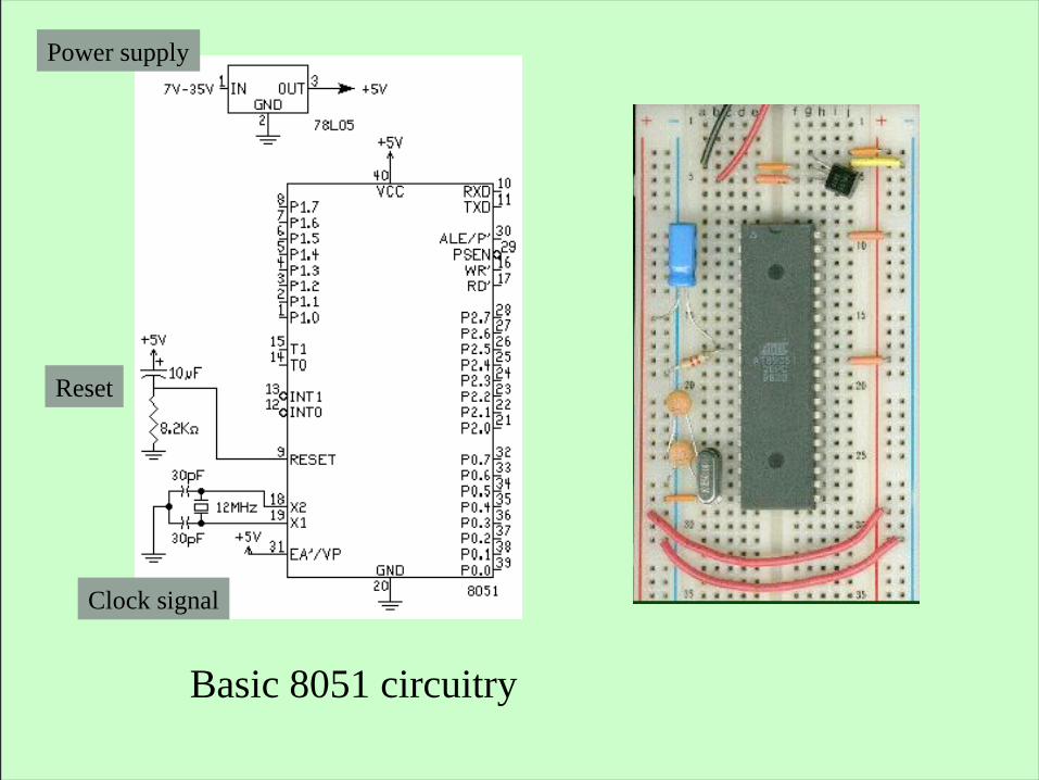
Basic 8051 circuitry
Power supply
Reset
Clock signal

Wednesday, February 25, 2015
Port 2
Port 0Port 1
Port 3

I/O Port Programming
• Port 1 is denoted by P1.
• P1.0 ~ P1.7• We use P1 as examples to show
the operations on ports.
• P1 as an output port (i.e., write CPU data to the external pin)
• P1 as an input port (i.e., read pin data into CPU bus)
Wednesday, February 25, 2015
Port 1( pins 1-8)

A Pin of Port 1
Wednesday, February 25, 2015
8051 IC
D Q
Clk Q
Vcc
Load(L1)
Read latch
Read pin
Write to latch
Internal CPU bus
M1
P1.X pinP1.X
TB1
TB2

Hardware Structure of I/O Pin
• Each pin of I/O ports
• Internal CPU bus:communicate with CPU
• A D latch store the value of this pin
• D latch is controlled by “Write to latch”• Write to latch= 1: write data
into the D latch
Wednesday, February 25, 2015
D Q
Clk Q
Vcc
Load(L1)
Read latch
Read pin
Write to latch
Internal CPU bus
M1
P1.X pin
P1.X
TB1
TB2

Hardware Structure of I/O Pin • 2 Tri-state buffer:
• TB1: controlled by “Read pin”• Read pin= 1: really read
the data present at the pin
• TB2: controlled by “Read latch”• Read latch= 1: read value
from internal latch
Wednesday, February 25, 2015
D Q
Clk Q
Vcc
Load(L1)
Read latch
Read pin
Write to latch
Internal CPU bus
M1
P1.X pin
P1.X
TB1
TB2
A transistor M1 gate Gate=0: open Gate=1: close

Tri-state Buffer
Wednesday, February 25, 2015
Output Input
Tri-state control (active high)
L H Low
Highimpedance (open-circuit)
HH
L H

Writing “1” to Output Pin P1.X
Wednesday, February 25, 2015
D Q
Clk Q
Vcc
Load(L1)
Read latch
Read pin
Write to latch
Internal CPU bus
M1
P1.X pinP1.X
8051 IC
2. output pin is Vcc1. write a 1 to the pin
1
0 output 1
TB1
TB2

Writing “0” to Output Pin P1.X
Wednesday, February 25, 2015
D Q
Clk Q
Vcc
Load(L1)
Read latch
Read pin
Write to latch
Internal CPU bus
M1
P1.X pinP1.X
8051 IC
2. output pin is ground1. write a 0 to the pin
0
1 output 0
TB1
TB2

Port 1 as Output(Write to a Port)• Send data to Port 1:
MOV A,#55H
BACK: MOV P1,A
ACALL DELAY
CPL A
SJMP BACK
• Let P1 toggle.• You can write to P1 directly.
Wednesday, February 25, 2015

Reading Input v.s. Port Latch • When reading ports, there are two possibilities:
• Read the status of the input pin. ( from external pin value)• MOV A, PX• JNB P2.1, TARGET ; jump if P2.1 is not set• JB P2.1, TARGET ; jump if P2.1 is set
• Read the internal latch of the output port.
• ANL P1, A ; P1 ← P1 AND A• ORL P1, A ; P1 ← P1 OR A• INC P1 ; increase P1
Wednesday, February 25, 2015

Reading “High” at Input Pin
Wednesday, February 25, 2015
D Q
Clk Q
Vcc
Load(L1)
Read latch
Read pin
Write to latch
Internal CPU bus
M1
P1.X pin
P1.X
8051 IC
2. MOV A,P1
external pin=High1. write a 1 to the pin MOV
P1,#0FFH
1
0
3. Read pin=1 Read latch=0 Write to latch=1
1
TB1
TB2
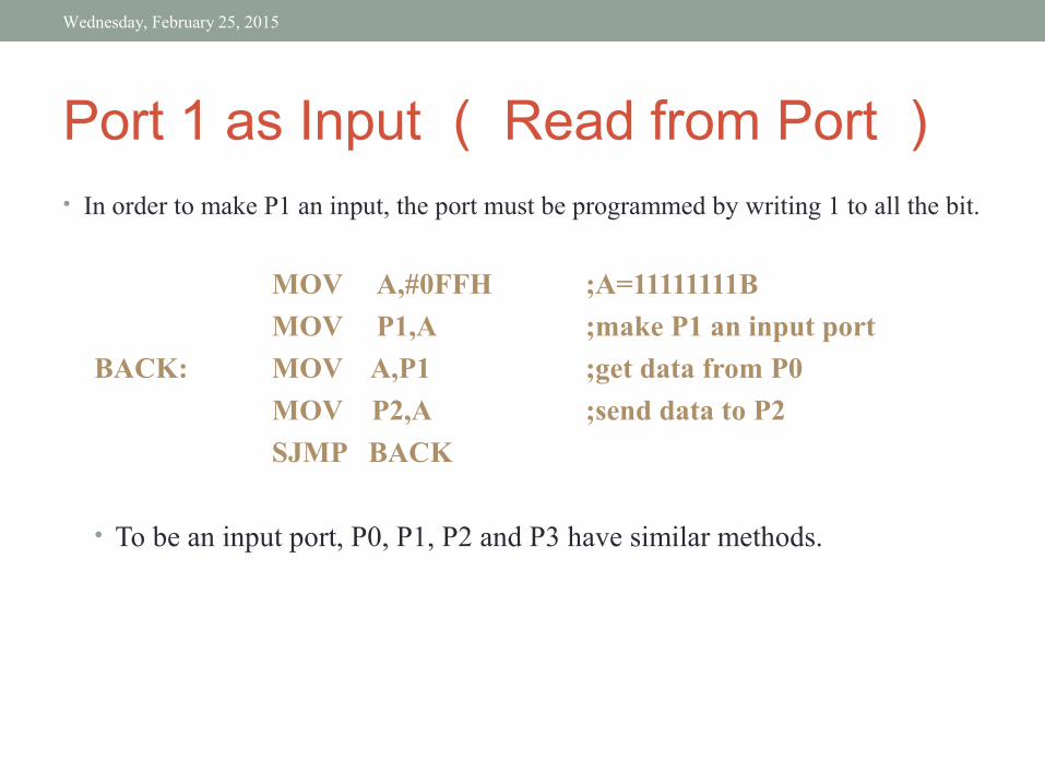
Port 1 as Input( Read from Port)• In order to make P1 an input, the port must be programmed by writing 1 to all the bit.
MOV A,#0FFH ;A=11111111B
MOV P1,A ;make P1 an input port
BACK: MOV A,P1 ;get data from P0
MOV P2,A ;send data to P2
SJMP BACK
• To be an input port, P0, P1, P2 and P3 have similar methods.
Wednesday, February 25, 2015

Instructions For Reading an Input Port
Mnemonics Examples Description
MOV A,PX MOV A,P2 Bring into A the data at P2 pins
JNB PX.Y,.. JNB P2.1,TARGET Jump if pin P2.1 is low
JB PX.Y,.. JB P1.3,TARGET Jump if pin P1.3 is high
MOV C,PX.Y MOV C,P2.4 Copy status of pin P2.4 to CY
Wednesday, February 25, 2015
• Following are instructions for reading external pins of ports:

Reading Latch• Exclusive-or the Port 1:
MOV P1,#55H ;P1=01010101
ORL P1,#0F0H ;P1=11110101
1. The read latch activates TB2 and bring the data from the Q latch into CPU.
• Read P1.0=0
2. CPU performs an operation.
• This data is ORed with bit 1 of register A. Get 1.
3. The latch is modified.
• D latch of P1.0 has value 1.
4. The result is written to the external pin.
• External pin (pin 1: P1.0) has value 1.
Wednesday, February 25, 2015

Reading the Latch
Wednesday, February 25, 2015
D Q
Clk Q
Vcc
Load(L1)
Read latch
Read pin
Write to latch
Internal CPU bus
M1
P1.X pin
P1.X
8051 IC
4. P1.X=12. CPU compute P1.X OR 1
0
0
1. Read pin=0 Read latch=1 Write to latch=0 (Assume P1.X=0 initially)
1
TB1
TB2
3. write result to latch
Read pin=0 Read latch=0 Write to latch=1
1
0

Read-modify-write Feature• Read-modify-write Instructions
• Check Mazidi’s• This features combines 3 actions in a single instruction:
1. CPU reads the latch of the port
2. CPU perform the operation
3. Modifying the latch
4. Writing to the pin• Note that 8 pins of P1 work independently.
Wednesday, February 25, 2015
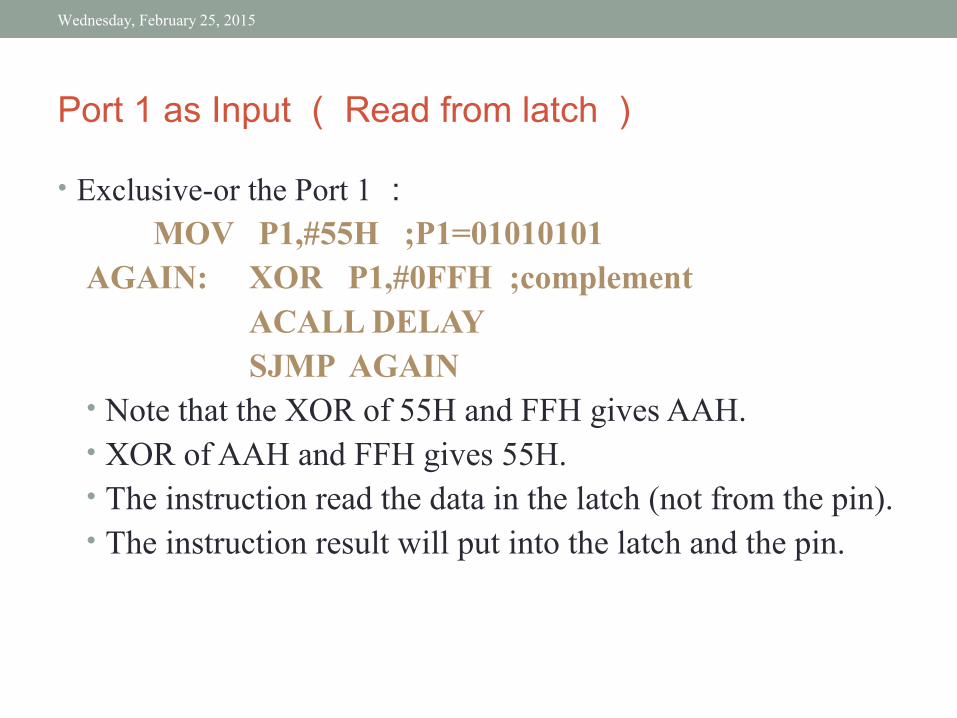
Port 1 as Input( Read from latch)
• Exclusive-or the Port 1: MOV P1,#55H ;P1=01010101AGAIN: XOR P1,#0FFH ;complement
ACALL DELAY SJMP AGAIN
• Note that the XOR of 55H and FFH gives AAH.• XOR of AAH and FFH gives 55H.• The instruction read the data in the latch (not from the pin).• The instruction result will put into the latch and the pin.
Wednesday, February 25, 2015
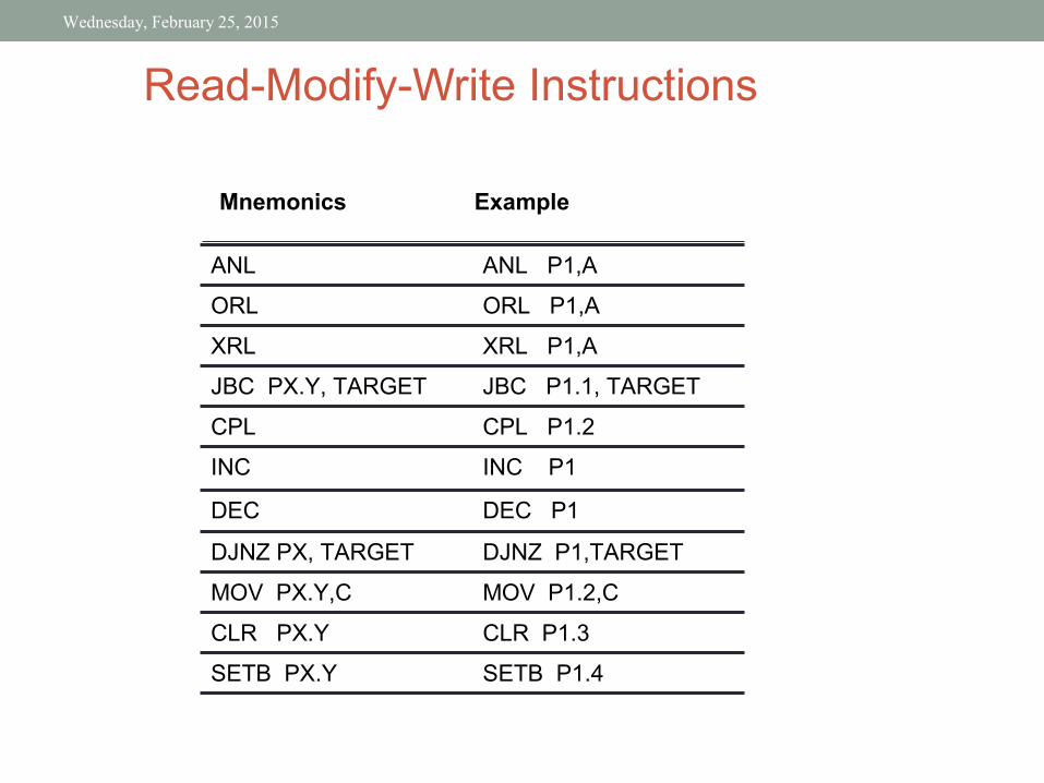
Read-Modify-Write Instructions
Wednesday, February 25, 2015
ExampleMnemonics
SETB P1.4SETB PX.Y
CLR P1.3CLR PX.Y
MOV P1.2,CMOV PX.Y,C
DJNZ P1,TARGETDJNZ PX, TARGET
INC P1INC
CPL P1.2CPL
JBC P1.1, TARGETJBC PX.Y, TARGET
XRL P1,AXRL
ORL P1,AORL
ANL P1,AANL
DEC P1DEC
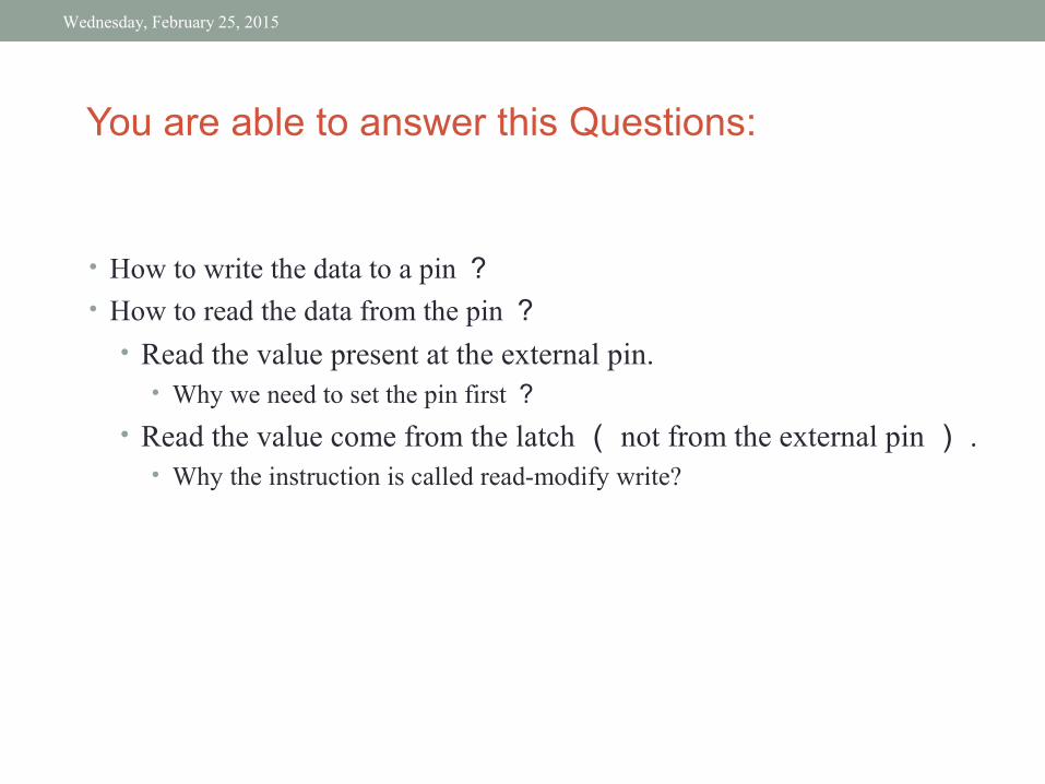
You are able to answer this Questions:
• How to write the data to a pin?• How to read the data from the pin?
• Read the value present at the external pin.• Why we need to set the pin first?
• Read the value come from the latch( not from the external pin) .• Why the instruction is called read-modify write?
Wednesday, February 25, 2015

Other Pins• P1, P2, and P3 have internal pull-up resisters.
• P1, P2, and P3 are not open drain.• P0 has no internal pull-up resistors and does not connects to Vcc inside the
8051.
• P0 is open drain.• Compare the figures of P1.X and P0.X.
• However, for a programmer, it is the same to program P0, P1, P2 and P3.• All the ports upon RESET are configured as output.
Wednesday, February 25, 2015

A Pin of Port 0
Wednesday, February 25, 2015
8051 IC
D Q
Clk Q
Read latch
Read pin
Write to latch
Internal CPU bus
M1
P0.X pinP1.X
TB1
TB2
P1.x

Port 0( pins 32-39)• P0 is an open drain.
• Open drain is a term used for MOS chips in the same way that open collector is used for TTL chips.
• When P0 is used for simple data I/O we must connect it to external pull-up resistors.
• Each pin of P0 must be connected externally to a 10K ohm pull-up resistor.
• With external pull-up resistors connected upon reset, port 0 is configured as an output port.
Wednesday, February 25, 2015

Port 0 with Pull-Up ResistorsWednesday, February 25, 2015
P0.0P0.1P0.2P0.3P0.4P0.5P0.6P0.7
DS5000
8751
8951
Vcc10 K
Port 0

Dual Role of Port 0
• When connecting an 8051/8031 to an external memory, the 8051 uses ports to send addresses and read instructions.
• 8031 is capable of accessing 64K bytes of external memory.
• 16-bit address: P0 provides both address A0-A7, P2 provides address A8-A15.
• Also, P0 provides data lines D0-D7. • When P0 is used for address/data multiplexing, it is connected
to the 74LS373 to latch the address.
• There is no need for external pull-up resistors.
Wednesday, February 25, 2015

74LS373
Wednesday, February 25, 2015
D
74LS373ALE
P0.0
P0.7
PSEN
A0
A7
D0
D7
P2.0
P2.7
A8
A15
OE
OC
EA
G
8051 ROM

Reading ROM (1/2)Wednesday, February 25, 2015
D
74LS373ALE
P0.0
P0.7
PSEN
A0
A7
D0
D7
P2.0
P2.7
A8
A12
OE
OC
EA
G
8051 ROM
1. Send address to ROM
2. 74373 latches the address and send to
ROM
Address
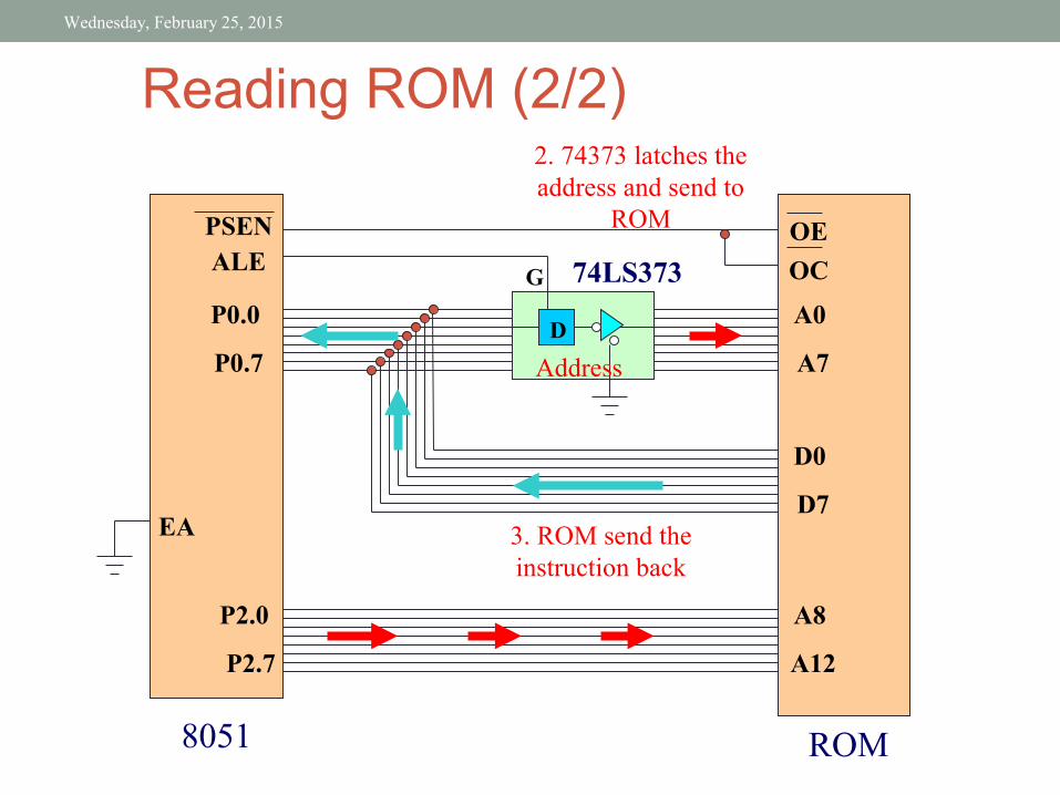
Reading ROM (2/2)
Wednesday, February 25, 2015
D
74LS373ALE
P0.0
P0.7
PSEN
A0
A7
D0
D7
P2.0
P2.7
A8
A12
OE
OC
EA
G
8051 ROM
2. 74373 latches the address and send to
ROM
Address
3. ROM send the instruction back

ALE Pin• The ALE pin is used for de-multiplexing the address and data
by connecting to the G pin of the 74LS373 latch.• When ALE=0, P0 provides data D0-D7.• When ALE=1, P0 provides address A0-A7.• The reason is to allow P0 to multiplex address and data.
Wednesday, February 25, 2015

Port 2( pins 21-28)• Port 2 does not need any pull-up resistors since it already has
pull-up resistors internally.• In an 8031-based system, P2 are used to provide address A8-
A15.
Wednesday, February 25, 2015
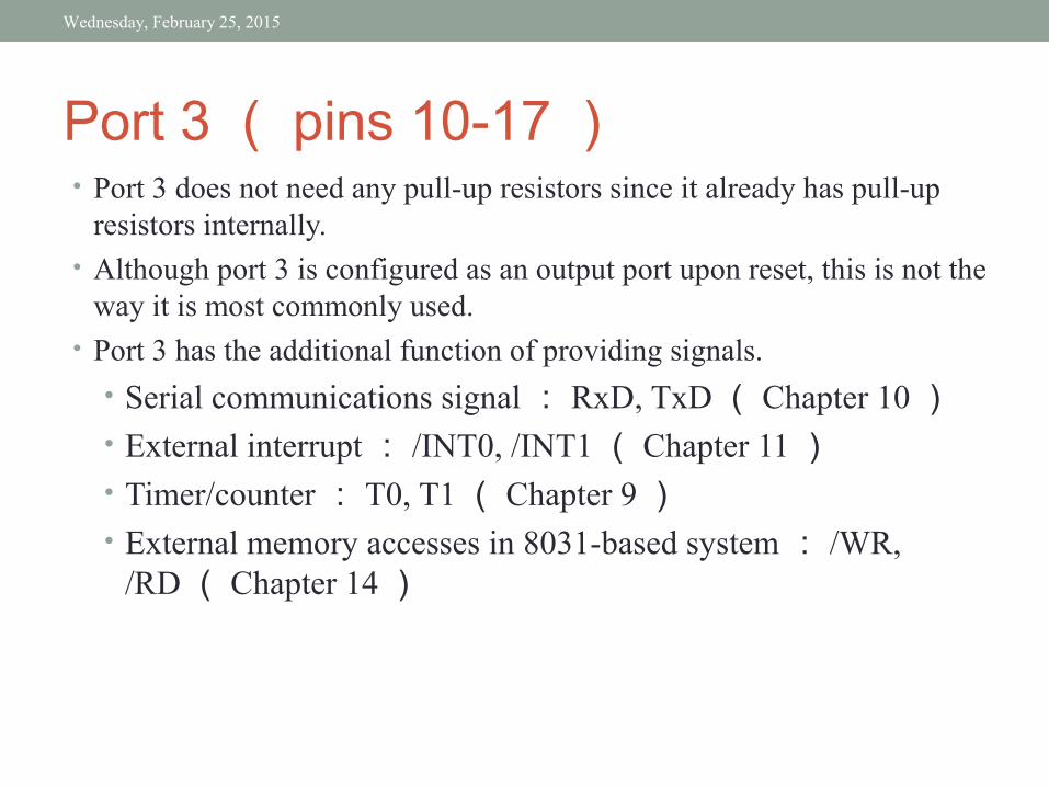
Port 3( pins 10-17)• Port 3 does not need any pull-up resistors since it already has pull-up
resistors internally.• Although port 3 is configured as an output port upon reset, this is not the
way it is most commonly used.• Port 3 has the additional function of providing signals.
• Serial communications signal: RxD, TxD( Chapter 10)• External interrupt: /INT0, /INT1( Chapter 11)• Timer/counter: T0, T1( Chapter 9)• External memory accesses in 8031-based system: /WR,
/RD( Chapter 14)
Wednesday, February 25, 2015
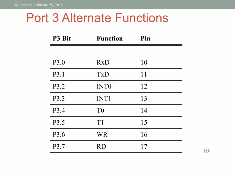
Port 3 Alternate FunctionsWednesday, February 25, 2015
17RDP3.7
16WRP3.6
15T1P3.5
14T0P3.4
13INT1P3.3
12INT0P3.2
11TxDP3.1
10RxDP3.0
PinFunctionP3 Bit