Advantech-LNC Technology Co., Ltd. LNC-M6800 SERIES I-NC ...
paper-tape form, as an alternative to buying a set of PROMs. A tape costs $15, and may be ordered direct from NS Elec-tronics, Cnr Stud Road and Mountain Highway, Bayswater, Victoria 3153.
Faster SC/MP chip, too National Semiconductor has also
announced a new N-channel version of the SC/MP chip itself. It offers three main features over the existing P-channel chip: Twice the speed, one quarter the power, and only a single + 5V supply.
Designated SC/MP-II, the new chip will be available in Australia shortly, from NS Electronics and their various distribu-tors in each state.
Microcomputer News & Products
SC/MP Tiny BASIC Back in the December 1976 issue, we
announced that National Semiconductor was coming out with a Tiny-BASIC interpreter for their SC/MP, called NIBL. At that stage only a 3k bytes preliminary version was available, with an improved 4k version still to come.
Well, the 4k version of NIBL has now arrived, and it's even better than was predicted. It is .now very much an extended Tiny-BASIC, with many power-ful features which should make it of great interest and value to professional and hobby computer users alike.
As predicted, it now offers an RND function to generate 16-bit random num-bers, and a LINK statement to allow call-ing machine language subroutines. The hoped-for DO . .. UNTIL statements are also provided, too.
In addition, there is now the ability to perform FOR ... NEXT loops as in many full BASICs. There is also the ability to handle character strings, and to handle hexadecimal constants. There is also a REM statement for remarks, a MOD function for absolute values, a STAT func-tion to return the current value of SC/MP's status register (allowing the program to manipulate flag and sense lines), and paging functions.
NIBL's formal grammar is now some-what more flexible, too, allowing greater programming efficiency. Multiple statements per line are now allowed, while LET is no longer mandatory in assignment statements.
And you can now buy NI BL in punched
New MC6800 kit Motorola Semiconductor Products has
released a new evaluation kit for their well-known MC6800 microprocessor. Called the MEK6800D2, the new kit has its own 24-key keyboard and 6-digit hex display, obviating the need for an expen-sive data terminal. It also features an inbuilt audio cassette interface, for con-venient program storage at low cost.
The kit comes with 256 bytes of RAM for user programs, a 1k byte ROM with a debug/monitor called MUG, and 16 lines of parallel I/O via a PIA. Provision is made for easy expansion.
By the time you read this, the new kits should be available from local Motorola distributors for around $240.
By courtesy of Motorola, EA has one of the new kits and we are currently put-ting it through its paces. We hope to publish the results next month, all going well.
ELECTRONICS Australia, April, 1977 73

MOTOROLA M6800 (ik EVALUATION KIT
MEK6800D2 provides a useful and expandable tool for those who wish to develop systems with the M6800 Microprocessor without investing in expensive terminals. All parts needed to complete the system and get up and running are provided in the kit with the exception of the power supply. In addition to the expansion available on the basic microcomputer module, additional RAM, ROM and I/O parts can be accommodated at a later date to implement more complex systems. Machine language programs can be entered through the system keyboard or via a built-in audio cassette interface system. Hexademical LED displays are provided for monitoring data and address information. A crystal-controlled clock generator is used to eliminate timing adjustments. • JBUG Monitor. Trace One Instruction. Set up to Five Breakpoints. Examine and Change Memory and Registers. • Parallel and Serial Interface Capability. • 16 I JO Lines, 4 Control Lines.
FIRMWARE FEATURES The monitor firmware included with this system sets a new standard of performance for evaluation kits. The function of the JBUG monitor is to allow the user to communicate with and hence control the M6800 microcomputer by using the hexadecimal keyboard and display module. The intelligence and diagnostic capability of JBUG is provided in line 1K x 8 ROM.
MEK6800 D2 HARDWARE FEATURES
Three I/O devices are provided in the kit. One Peripheral Interface Adapter (PIA) is dedicated to the hexadecimal keyboard and display module. A second PIA is made available exclusively for the user. An Asynchronous Com-munications Interface Adapter (ACIA) is also included to interface with your audio cassette tape recorder.
WANT TO HEAR MORE? CALL MOTOROLA SYDNEY
—438 1955, 43 4299 MELBOURNE-561 3555
MOTOROLA DISTRIBUTORS
TOTAL ELECTRONICS MELBOURNE 96 2891; SYDNEY 439 6722; BRISBANE 229 1633; ADELAIDE 268 2922; PERTH (ATHOL HILL P/L) 25 7811; NEWCASTLE (DIGITRONICS) 69 2040; CANBERRA (ELECTRONIC COMP) 95 6811;
CEMA MELBOURNE 877 5311; SYDNEY 439 4655; BRISBANE (ELECTRONIC COMP) 371 5677; ADELAIDE (WOOLLARD & CRABBE) 51 4713; CANBERRA (CUSTOM SCIENTIFIC) 47 6179; WOLLONGONG (MACELEC) 29 1276; PERTH (RESERVE ELECTRONICS) 87 1026;
MOTOROLA Microsystems —making it happen in microcomputers
ELECTRONICS Australia, May, 1977 73

A9 18
A8 17
A7 16
A6 15
t
H
A5 A4 14 13
A
A3 A2 Al AO 12 11 10 9
t I t t t
Program Counter
Output Buffers
A15 A14 A13 25 24 23
ft' Al2 All A10 22 20 19
t
Output Buffers
Vcc = Pin 8 VSS = Pins 1,21
•26 27 28 29 30 31 32 33
07 06 D5 D4 03 D2 D1 190
82 ELECTRONICS Australia, May, 1977
GETTING INTO MICROPROCESSORS
The Motorola 6800
Motorola Semiconductor Products were only the second major US manu-facturer to enter the microprocessor field, in 1974. The MC6800 was their initial entry, and the fact that it is still one of the market leaders—and showing no signs of giving ground—testifies to the soundness of the basic design concept. Needless to say it is now supported by a large amount of development and applications software, much of it generated by users. This inevitably increases its appeal for potential new users, compared with newer entries to the field.
It is strongly supported in another sense, too: along with the basic micro-processor chip there are a number of matching memory and interfacing chips, all designed to simplify system design. These include a 1024 x 8-bit ROM (MCM6830), a 128 x 8-bit RAM (MCM6810), a programmable 16-bit bidirectional Peripheral Interface Adap-
Clock, 01 3 ---11.
Clock, 02 37
Reset 40
Non-Maskable Interrupt 6 (1.
Halt 2 -IP Instruction
Interrupt Request 4
Decode and Pointer
Stack
Three-State Control 39 Control
Data Bus Enable 36 0.
Bus Available 7
Valid Memory Address 5 10
Read/Write 34
Instruction Register
Data Buffer
for or "PIA" (MC6820), a programmable Asynchronous Communications Inter-face Adaptor or "ACIA" (MC6850), a programmable Synchronous Serial Data Adaptor or "SSDA" (MC6852), and a number of more specialised devices including some which are still in development. There are also various sys-tem housekeeping devices, including a family of hybrid clock oscillators.
As the block diagram suggests, the basic architecture of the MC6800 micro-processor chip itself is fairly straight-forward. This is perhaps part of the secret of its success, although there are a num-ber of subtle strengths which also emerge upon closer inspection.
There are only six internal working registers, one of which is a condition code or processor status register. Two of the remaining registers are 8-bit accumulators, both full primary accum-ulators of almost equal status. The other three registers are the program counter,
an index register and a stack pointer, all three of which are 16 bits long. The MC6800 implements its stack in external RAM.
The status register has six active bits, one of which is the flag for enabling and disabling the master interrupt input. The remaining status bits are condition code flags, representing arithmetic carry and overflow, sign, zero and a bit-3 carry used for BCD arithmetic. None of the sta-tus register bits is accessible directly via external device pins.
Data and address information pass between the MC6800 and the rest of a system via two separate buses. One is an 8-bit bidirectional data bus; the other is a 16-bit address bus which gives the MC6800 the capability of directly addressing 65,536 or "65k" bytes of memory space.
The output buffers on both the data and address lines are 3-state, and may be disabled for DMA operation.
There is no clock oscillator on the MC6800 chip itself. Instead there are two clock input pins, which must be fed with non-overlapping two-phase clock sig-nals. Maximum clock frequency is 1MHz, and a machine cycle corresponds direc-tly to a clock period. Fetching and execu-tion of an instruction ranges from 2 to 12 machine cycles depending upon the instruction, or from 2 to 12us at the maximum clock rate.
Incidentally the MC6800 is an N-channel depletion mode MOS device, made using silicon gate technology. As a result it operates from a single +5V supply.
Apart from the normal reset and mas-ter interrupt inputs the MC6800 is also provided with a non-maskable interrupt input. There is also a software-interrupt instruction, for program abortion. Vec-toring is provided only for the different interrupt mechanisms; within each mechanism an interrupt source must be identified by polling.
What the MC6800 does do upon being interrupted is automatically save the con-tents of all its registers on the stack, in external RAM. This takes place in only 10 machine cycles, far less than would be required if the interrupt routine had to perform the saving by explicit instruc-tions (required by most other micros).
Left: Basic architecture of the MC6800 microprocessor chip. Six registers are accessible to the programmer.
One of the most established microprocessors, the Motorola MC6800 is supported by a continuously expanding "family" of memory and specialised interfacing chips—and also by a great deal of proven soft-ware and applications experience. In this article we look at the MC6800, its main support chips, and also the recently released MEK6800D2 "Mark II" evaluation kit.
by JAMIESON ROWE
Program Counter
Index Register
Accumulator A
Accumulator B
Condition Code
Register
Index Register
Stack Pointer
ALU
11
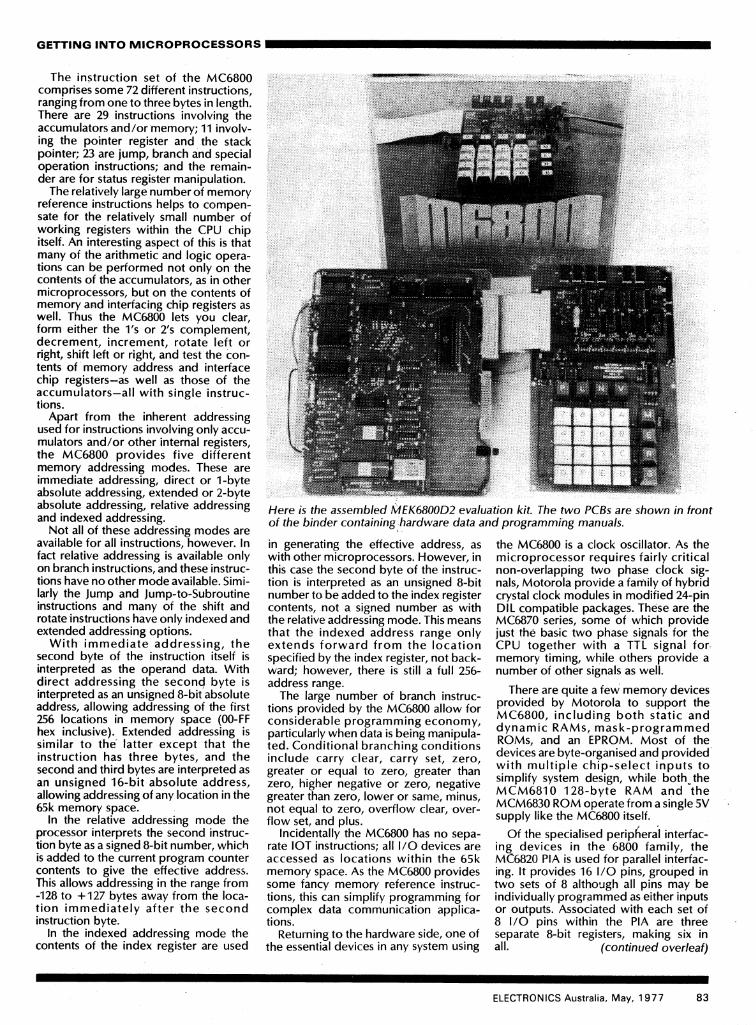
Here is the assembled MEK6800D2 evaluation kit. The two PCBs are shown in front of the binder containing hardware data and programming manuals.
GETTING INTO MICROPROCESSORS
The instruction set of the MC6800 comprises some 72 different instructions, ranging from one to three bytes in length. There are 29 instructions involving the accumulators and/or memory; 11 involv-ing the pointer register and the stack pointer; 23 are jump, branch and special operation instructions; and the remain-der are for status register manipulation.
The relatively large number of memory reference instructions helps to compen-sate for the relatively small number of working registers within the CPU chip itself. An interesting aspect of this is that many of the arithmetic and logic opera-tions can be performed not only on the contents of the accumulators, as in other microprocessors, but on the contents of memory and interfacing chip registers as well. Thus the MC6800 lets you clear, form either the l's or 2's complement, decrement, increment, rotate left or right, shift left or right, and test the con-tents of memory address and interface chip registers—as well as those of the accumulators—all with single instruc-tions.
Apart from the inherent addressing used for instructions involving only accu-mulators and/or other internal registers, the MC6800 provides five different memory addressing modes. These are immediate addressing, direct or 1-byte absolute addressing, extended or 2-byte absolute addressing, relative addressing and indexed addressing.
Not all of these addressing modes are available for all instructions, however. In fact relative addressing is available only on branch instructions, and these instruc-tions have no other mode available. Simi-larly the Jump and Jump-to-Subroutine instructions and many of the shift and rotate instructions have only indexed and extended addressing options.
With immediate addressing, the second byte of the instruction itself is interpreted as the operand data. With direct addressing the second byte is interpreted as an unsigned 8-bit absolute address, allowing addressing of the first 256 locations in memory space (00-FF hex inclusive). Extended addressing is similar to the latter except that the instruction has three bytes, and the second and third bytes are interpreted as an unsigned 16-bit absolute address, allowing addressing of any location in the 65k memory space.
In the relative addressing mode the processor interprets the second instruc-tion byte as a signed 8-bit number, which is added to the current program counter contents to give the effective address. This allows addressing in the range from -128 to +127 bytes away from the loca-tion immediately after the second instruction byte.
In the indexed addressing mode the contents of the index register are used
in generating the effective address, as with other microprocessors. However, in this case the second byte of the instruc-tion is interpreted as an unsigned 8-bit number to be added to the index register contents, not a signed number as with the relative addressing mode. This means that the indexed address range only extends forward from the location specified by the index register, not back-ward; however, there is still a full 256-address range.
The large number of branch instruc-tions provided by the MC6800 allow for considerable programming economy, particularly when data is being manipula-ted. Conditional branching conditions include carry clear, carry set, zero, greater or equal to zero, greater than zero, higher negative or zero, negative greater than zero, lower or same, minus, not equal to zero, overflow clear, over-flow set, and plus.
Incidentally the MC6800 has no sepa-rate IOT instructions; all I/O devices are accessed as locations within the 65k memory space. As the MC6800 provides some fancy memory reference instruc-tions, this can simplify programming for complex data communication applica-tions.
Returning to the hardware side, one of the essential devices in any system using
the MC6800 is a clock oscillator. As the microprocessor requires fairly critical non-overlapping two phase clock sig-nals, Motorola provide a family of hybrid crystal clock modules in modified 24-pin DI L compatible packages. These are the MC6870 series, some of which provide just the basic two phase signals for the CPU together with a TTL signal for memory timing, while others provide a number of other signals as well.
There are quite a few memory devices provided by Motorola to support the MC6800, including both static and dynamic RAMs, mask-programmed ROMs, and an EPROM. Most of the devices are byte-organised and provided-with multiple chip-select inputs to simplify system design, while both_ the MCM6810 128-byte RAM and the MCM6830 ROM operate from a single 5V supply like the MC6800 itself.
,• Of the specialised peripheral interfac-
ing devices in the 6800 family, the MC6820 PIA is used for parallel interfac-ing. It provides 16 I/O pins, grouped in two sets of 8 although all pins may be individually programmed as either inputs or outputs. Associated with each set of 8 I/O pins within the PIA are three separate 8-bit registers, making six in all. (continued overleaf)
ELECTRONICS Australia, May, 1977 83
GETTING INTO MICROPROCESSORS
One in each group is a data buffer, another a latch whose bits specify whether the device pins are used as inputs or outputs; the third is a control register used to define interfacing pro-tocol and status. All six PIA registers are addressable in MC6800 memory space, although in a slightly confusing manner: the control registers are addressed directly, while the data and direction registers share common addresses and must be distinguished by setting a con-trol register bit.
The other peripheral interfacing device most likely to be found in smaller 6800 systems is the MC6850 ACIA, used for asynchronous serial interfacing. The ACIA is rather like a UART, having separate sections for asynchronous transmission and reception. However unlike a UART these share a common 8-bit parallel bidirectional interface to the 6800 system data bus. In addition, there is an 8-bit control register address-able separately in 6800 memory space, which allows program control of serial data format, a choice of three com-munication rate clock division ratios, and the handshaking protocol. There is also a status register, sharing the same address as the control register, whose bits may be read to determine ACIA status.
Having looked briefly at the MC6800 microprocessor, its instruction set and some of its support chips, let us now turn to the new MEK6800D2 evaluation kit. This has been produced by Motorola to provide a complete low-cost 6800 sys-tem, for both evaluation and basic program development.
The MEK6800D2 is an assemble-it yourself kit, which goes together tc produce two PCB assemblies. One is the microcomputer itself, on a PCB measur-ing 248 x 210mm overall; the other is low-cost terminal unit on a PCB measuring 254 x 159mm.
The assembled microcomputer board has the MC6800 itself, a crystal clock module (614.4k Hz), a 1 k byte ROM with resident "JBUG" monitor program, three 128-byte RAMs (one of which is alloca-ted to the monitor, leaving 256 bytes for user programs), two PIA devices and an ACIA.
The PCB also has decoding and sockets for easy expansion using a further two 128-byte RAMs, and two 1k byte EPROMs (MCM68708). It also has space for data bus and address bus buf-fers, if the user wishes to expand further into a multi-board system.
The assembled "terminal" ,PCB has a 24-key keyboard and a display using six 7-segment LEDs. Together these can be used with the JBUG monitor for entering programs, examining memory and regis-ters, single stepping through a program, setting and removing breakpoints (five
84 ELECTRONICS Australia, May, 1977

SIMPLE DI SPLAY PROGRAM FOR MOTOROLA MEK6800D2 KIT WRITTEN BY J. ROWE, ELECTRONICS AUSTRALIA 9. 3. 1977
0000 CE 00 24 START, L DX DI SBUF SET X AS BUFF PTR 0003 DF 22 STX XBUF & SAVE 0005 86 20 L DA A $20 SET PIA FOR DI SPLAY U 1 0007 B7 80 22 STA A DI SREG 000A A6 00 LOOP,LDA A 0,X FETCH CHAR VIA X 000C B7 80 20 STA A SEG REG & DI SPLAY 000F CE 00 4D L DX $4D SET UP X FOR 1MS DELAY 0012 BD E0 E0 J SR DLY 1 CALL JBUG DELAY S- R 0015 7C 00 23 INC XBUF+ 1 INCREMENT SAVED BUFF PTR 0018 DE 22 L DX XBUF & RESTORE TO - X 00 1A OC CL C CLEAR CARRY 001B 74 SO 22 LSR DI GREG UPDATE DIGIT PTR IN PI A 001E 24 EA BCC LOOP CONTINUE UNTIL 6 DONE 0020 20 DE BRA START BACK TO BEGIN AGAIN 0022 00 00 XBUF, X I S STORED HERE 0024 02 START OF MESSAGE BUFFER 0025 00 0026 40 0027 40 0028 21 0029 24
A simple novelty program for the MEK6800D2 kit. It displays encoded characters stored in locations 0024-0029 on the kit's 6-digit LED display.
GETTING INTO MICROPROCESSORS
are permitted), and transferring control to the user program.
In addition, the terminal PCB contains a full audio tape interface, to allow dumping and loading of programs using a normal cassette or reel-to-reel tape recorder. All that is required apart from the kit (and power supply) are a couple of shielded leads with suitable audio connectors.
The loading and dumping operations are controlled by further JBUG routines. Transfer takes place at a rate of 300 bauds, and the format conforms to the "Kansas City Standard" with 2400/ 1200Hz tones. The interfacing circuitry requires no "tweaking", using a stable counter-type decoder.
The terminal PCB connects to the main .microcomputer PCB by means of a 50-way flat ribbon cable and edge con-nector. The keyboard and LED display interface via one of the two PIAs, while the tape interface uses the ACIA. The remaining PIA on the main PCB is avail-able for user interfacing, with the ter-minal connected. If the user later decides to use the kit for a dedicated application, without the terminal PCB, all three inter-facing chips can be used for interfacing.
It is also possible to convert the kit over for operation with a teleprinter or other serial asynchronous terminal. The main change required is to replace the MUG ROM with another containing the terminal-orientated monitor "MINIbug Ill
The complete MEK6800D2 kit operates from a single +5V power sup-ply, drawing about -I amp.
The Sydney office of Motorola Semi-conductor sent us one of the MEK6800D2 kits, so that we would be able to assemble it and report to readers on our findings.
The kit comes in a single box, which opens to reveal one of the large spring-clip binders. Inside are two blister packs containing most of the parts for the two PCB modules, together with a plastic bag containing the rest of the parts. There are also a number of handbooks, including a kit manual, programming reference manual and M6800 system design book.
I found it fairly easy to put the kit together, although the instructions are rather cursory and assume that the builder has a fair amount of experience. Assembly took me about 7 hours, but I wasn't trying to break any records.
The kit worked perfectly when power was applied, and I was then able to run through the introductory program load-run-debug example which Motorola have thoughtfully provided in the kit manual. This is well done, and should give a newcomer to microcomputer sys-tems a good idea of the basic concepts of program manipulation via a monitor.
When it came to writing our own
programs, the going wasn't quite as easy. The programming reference manual doesn't seem to me to be particularly well written, at least as far as the introductory material is concerned. For example the material describing the various 6800 addressing modes complicates the issue by talking quite a lot about assembly language syntax, so that a beginner could get very con-fused.
As I was not too familiar with the 6800, it took a while to sort out chip operation from assembler operation. One thing which helped was a look through the list-ing for the kit's J-BUG monitor program, which Motorola have thoughfully given in the manual.
Once the addressing modes were sorted out, I was able to begin writing a few short programs and try them out. A sample program is reproduced here, as readers may find it interesting. It was written as a little exercise to see how one can use the LED display under user pro-gram control.
The kit manual doesn't help a great deal in telling you how to display data, so I had to deduce the way of doing this from the terminal circuit diagram and the J-BUG listing. It turns out that the rou-tines in J-BUG itself are not capable of being called by user programs, as they are not self-contained subroutines. However, in any case it is fairly easy to provide a routine in one's own program, as you can see. This is largely because the PIA does most of the work.
The comments in the right-hand column of the listing should give you a fair idea how the program works. Note that the display digit multiplexing is per-
formed by loading a 1 into one data register of the PIA, labelled "DIGREG", and then shifting the 1 along using the LSR instruction (address 001B). Similarly the actual digits are fed to the display segments by loading them into the other PIA data register, labelled "SEGREG".
The only part of the J-BUG monitor made use of by this little program is the subroutine DLY1, used to obtain the 1ms delay between displayed digits. This is used by first loading the index register with hex 4D, to specify a 1ms delay time, and then calling the subroutine at address E0E0. The two instructions invol-ved are those with their first bytes stored in addresses 000F and 0012.
Note that the simple 6-character mes-sage displayed by this program is stored in locations 0024-0029. They are not in ASCII code, but in a code whose first 7 bits correspond to the seven display seg-ments, in complement form. Any characters capable of being displayed on 7-segment LEDs can be shown, by work-ing out the appropriate codes.
To summarise, the MEK6800D2 kit seems a well-designed one, and should enable those with reasonable experience at electronic kit building to build up a low-cost 6800 system. When assembled it becomes a small but businesslike development system, adequate for learning 6800 programming and working up quite respectable programs. And with plenty of provision for expansion, you can make it grow into a more elaborate system when this is needed.
In short, good value for money at the quoted price of around $240. The kit should be available from Motorola dis-tributors, in every state.
ff
ELECTRONICS Australia, May, 1977 85
Using the Motorola D2 kit with a terminal Computer hobbyists and schools who have the Motorola MEK6800D2 evaluation kit should find this article interesting. It ex-plains how the kit may be converted easily and with minimum out-lay to interface with a video terminal or teleprinter, using standard 20mA current loops. It also gives details of useful subroutines available in the terminal-orientated MINIBUG-lll ROM.
Since we wrote about the Motorola MEK6800D2 "Mark 2" evaluation kit in the May 1977 issue, quite a few of the kits have apparently been sold. It would seem that many people agreed with our basic finding, that the kit provided an attractive way of building up a 6800-based system suitable for learning 6800 programming and working on program development.
Probably one of the features that appealed to people was the kit's expan-dability. For example although it comes with only 256 bytes of user-available RAM, the PCB provides decoding and sockets for the addition of a further 256 bytes merely by plugging in a further pair of MCM6810 RAM chips. There are also two further sockets, which may be arranged quite easily to accept either a pair of 1024-byte EPROMs (2708 Or similar), or a pair of 2048-byte mask-programmed ROMs (MCM68316 or similar).
To allow for still further expansion the PCB is provided with spaces for the addition of data and address bus buffers, so that external memory boards and further peripheral inter-faces may be connected. As the kit already offers two MC6820 PIA (peripheral interface adapter) devices, each providing two 8-bit bidirectional peripheral interface ports, and an MC6850 ACIA (asynchronous com-munications interface adapter) which provides a serial input and output, this makes it, very suitable for expansion into a full-scale minicomputer or development system.
Motorola itself makes available a number of compatible memory boards, including two dynamic RAM boards offering either 4096 bytes or 16,384 bytes of memory (MM6 8 1 0 0, MMS68104). However these are
probably a little elaborate for most hobbyists, being more suitable for the professional user. A more attractive ap-proach for the hobbyist would probably be to use one of the low cost memory modules now available using static RAM chips.
Apart from memory expansion, perhaps the most likely thing that both hobbyist and professional D2 kit users will want to do to their system is modify it for use with a video terminal or teleprinter. Although the original 24-key. keyboard and LED-display "ter-minal" supplied with the kit is quite sufficient for one's initial foray into 680Q system operation and develop-ment of simple programs, it is not really suitable for serious work. Programs may be stored on cassette tape, but cannot
by JAMIESON ROWE
be entered efficiently in the first place or listed conveniently for examination. Word processing and games are not really feasible with the simple terminal, either.
Anticipating that many users would want to modify their D2 kit for use with a standard terminal, Motorola has made available a suitable terminal-orientated debug/monitor program. The debug/monitor is called "MINIBUG-III", and it comes in a mask-programmed ROM which is pin-compatible with the original JBUG monitor ROM supplied as part of the D2 kit.
The firm has also made available an application note (AN-771), giving details of the ways that the D2 kit may be expanded, and including informa-
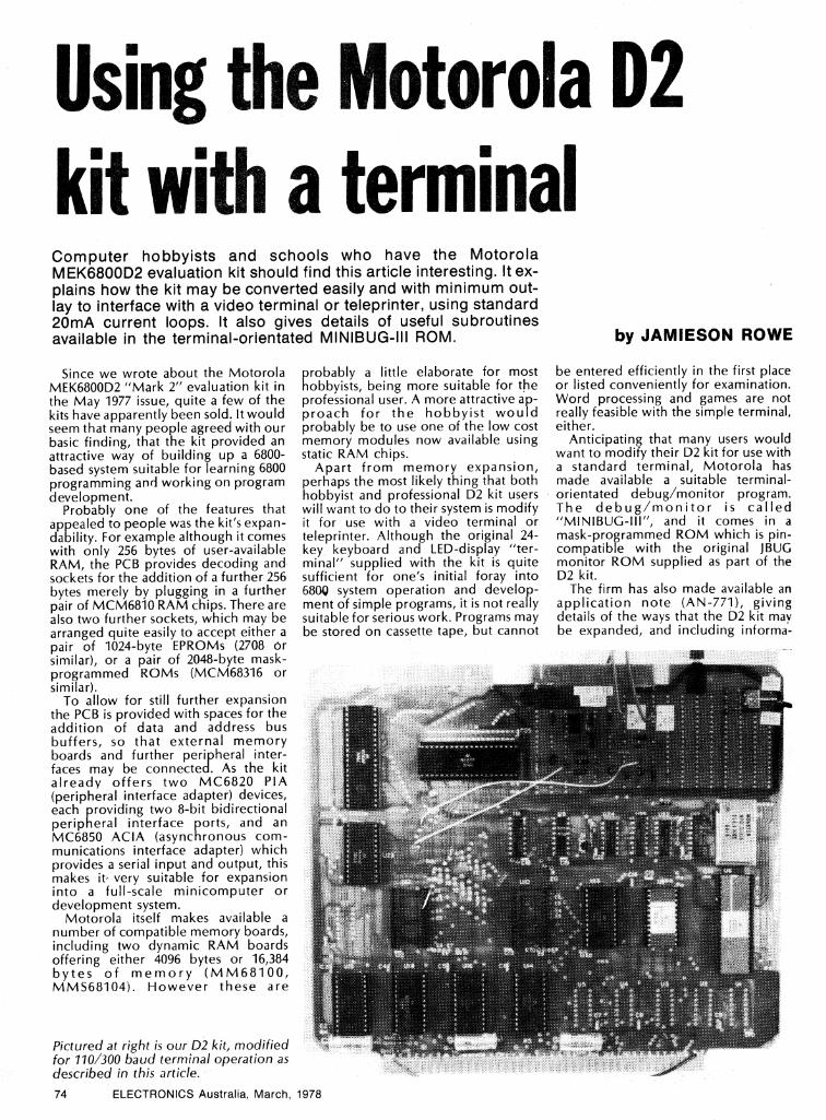
Pictured at right is our D2 kit, modified for 110/300 baud terminal operation as described in this article.
74 ELECTRONICS Australia, March, 1978

gatalltilliffinonagapippoppir +-5V
RTS
RXD ACIA (U23)
TXD
TXC
RXC
MOW
(CUT)
1111111111114z FROM wer (MN 13)-A.
MC-14040
J2
SIMPLE 20mA SERIAL INTERFACE FOR MOTOROLA MEK6800D2 KIT (TO SUIT MINIBUG III ROM)
19
Details of the circuit modifications required for using the D2 kit with a 20mA video terminal or teleprinter. The 555 provides the 110-baud clock.
non on modification of the kit for use with a terminal. The application note is available on request to professional users, but not to hobbyists. In any case it is intended primarily for the professional, dealing mainly with fairly elaborate expansion techniques and in many places providing only very cur-sory explanations.
The details given for interfacing to a terminal assume that the user will want to implement a dual-monitor system, wherein both the MUG and MI IBUG 111 monitor ROMs are in circuit and alternatively selectable by means of 'either a hardware switch or software in-structions. It seems unlikely that many hobbyists will want to go that far. Also shown is the use of opto-couplers for full electrical isolation of the terminal interfacing; as most hobbyists will be using video terminals with opto-couplers already fitted, this is really not necessary.
Actually if you simply want to imple-ment a basic system, using just the MINIBUG-Ill ROM and low-cost inter-facing to a standard 110-baud or 300-baud terminal, the application, note isn't very helpful. You're apparently ex-pected to work out the details for yourself.
Having gone through this exercise myself the hard way, I thought readers might like to benefit from my ex-perience. It turns out that apart from the replacement ROM with MINIBUG-111, all you need are three low-cost tran-ostors, a 555 timer IC and a few minor romponents.
The modifications and circuit ad-ditions are shown in the circuit. For convenience they can be split into two distinct sections: that associated with actual interfacing to the terminal, and that concerned with setting the com-munications baud rate.
The MINIBUG-III monitor program is designed to communicate with the ter-minal via the MC6850 ACIA device, labelled "U23" on the D2 kit PCB. The ACIA is similar to a UART, except that is bus orientated: the data format and clock ,divider rate are software programmable, while the transmitter and receiver status are available for software interrogation.
Data from the computer emerges in asynchronous serial form from the transmitter section of the ACIA at the "transmit data" (TXD) output, pin 6. This also connects to the )2 output con-nector of the kit PCB, at pad U. The data at this point is in TTL voltage-level form: logic high level corresponds to "mark", and logic low level to "space".
In order to drive a standard video ter-minal or teleprinter this voltage-level signal must be converted into the equivalent 20mA current-loop signal, with "mark" corresponding to 20mA DC current flow and "space" to zero current. This is done by the additional circuitry using transistors Q1 and Q2.
Transistor Q1 is driven from the TXD output of the ACIA, so that when the TXD output is at the high logic level for "mark", Q1 is driven into saturation. This causes transistor Q2 to be driven into conduction also, passing current to the display/printer section of the ter-
minal. The 180-ohm resistor sets the current level to the nominal 20mA figure required.
When the TXD output of the ACIA falls to the logic low level for "space", transistor Q1 cuts off. This causes Q2 to cut off also, interrupting the loop current. Hence Q1 and Q2 provide a simple TTL voltage level to 20mA current loop interface.
The serial input of the receiver sec-tion of the ACIA is its "receiver data in-
ut" (RXD), pin 2. This also connects to pad W on PCB connector )2, in the D2 kit. Like the transmitter output, the RXD input is designed to accept TTL voltage logic levels, with logic high cor-responding to "mark" and logic low to "space".
As the keyboard output of a video terminal or teleprinter is basically a set of switch contacts (either mechanical or solid state) which are closed for "mark" and open for "space", a conversion cir-cuit is again needed in order to produce the TTL levels required by the ACIA. This conversion is performed by the additional circuitry shown around transistor Q3.
Essentially the circuit consists of an inverter stage using Q3, with its base potentially forward biased via the 3.3k and two 1k resistors. However the keyboard switch is connected so that when closed for "mark", it shorts out the forward bias and causes Q3 to be cut off. The 4.7k collector resistor of Q3 thus pulls the RXD input of the ACIA to the corresponding logic high level.
When the keyboard switch opens for "space", however, the forward bias is applied to Q3 and the transistor is driven into saturation. This pulls the RXD input of the ACIA down to the corresponding logic low level.
The 0.1uF capacitor is used in con-junction with the 3.3k resistor as a filter to suppress any contact bounce that may occur with teleprinter keyboards. The filtering is not strictly necessary with video terminals having a solid state switch or opto-coupler on the keyboard output, although I suggest you leave it in because it filters any hum which may be induced into the cable.
The two diodes are top rotect the transistor from any "spikes" which may be generated in the cable due to induc-tion or the effects of cable inductance. Again they are not strictly necessary if you are using a cable only a few feet long — particularly if it is shielded — but I suggest you leave them in as they only cost a few cents.
The circuitry associated with Q1, Q2 and Q3 thus performs the actual ter-minal interfacing. The remaining part of the circuitry added to the D2 kit is used to provide the ACIA with the ap-propriate clock signals, so that it can operate on the data rates of 110 or 300 baud expected by the MINIBUG-III monitor program and most video ter-minals and teleprinters.
In the D2 kit as originally wired ac-
ELECTRONICS Australia, March, 1978 75
Using the Motorola D2 kit with a termina II • •
cording to the Motorola manual, the ACIA is used with an audio FSK (fre-quency shift keying) interface on the matching "terminal" PCB, for dumping on and loading programs from cassette tapes. The data rate used is 300 baud, and the corresponding 4800Hz clock signal required by the ACIA transmitter 06 times 300) is derived from U17. This
an MC14040 multi-stage binary diYider IC, driven in turn by a 12288MHz signal from the MC6871 crystal clock generator (U15).
As originally wired the 4800Hz signal connects to ACIA pin 4, the transmitter dock input (TXC). The receiver clock input RXC (pin 3) is fed with a recovered 4800Hz clock signal, derived tr4 the FSK interface from the tape recording itself.
To use the ACIA with a standard video terminal or teleprinter, it is necessary to connect the TXC and RXC inputs of the ACIA together so that they operate at the same clock rate. This is most easily done by joining the two together with a wire link near the 12 edge connector. The two clock in-puts run to connector pads 17 and 19, and they can be joined easily near the pads.
As the TXC input is still at this stage connected to U17 via the PCB pattern, the link between the TXC and RXC in-puts of the ACIA will enable the system to communicate with a terminal at a fix-ed, crystal-locked 300 baud rate.
The MINIBUG-III monitor ROM can communicate at this rate, as can many video terminals and some teleprinters. However with MINIBUG-III it is actual-ly necessary to use 110-baud com-munication at least upon initial switch-on, in order to tell the monitor to change to 300-baud operation. For this reason and to allow the system to work with 110-baud terminals, it is necessary to modify the clock feed circuit.
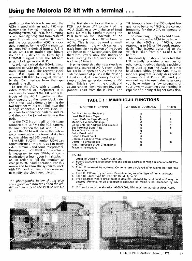
The photographs below should give you a good idea how we added the ad-ditional circuitry to the PCB of our D2 kit.
The first step is to cut the existing PCB track from U17 to pin 4 of the ACIA (U23), to allow a choice of baud rates. Do this by carefully cutting the PCB track on the underside of the board, at a point about 30mm from the ACIA. This is just beyond a small plated-through hole which carries the track from pin 4 to the top of the board and hence to the J2 connector. The cut therefore severs only the underside track leading to U17, and leaves the track to J2 intact.
Having done this the next step is to provide a source of ACIA clock pulses for 110-baud operation. As there is no suitable source of pulses in the existing D2 kit circuit, it is necessary to add a simple pulse generator using a 555 timer. This is shown in the circuit, and as you can see it involves very few com-ponents apart from the IC itself. The
22k trimpot allows the 555 output fre-quency to be set to 1760Hz, the correct frequency for the ACIA to operate at 110 baud.
The remaining thing is to add a small switch, to allow the ACIA to be fed with either the 4800Hz or 1760Hz, cor-responding to 300 or 110 bauds respec-tively. The 4800Hz signal fed to the switch is taken from pin 13 of U17, as before.
Incidentally, it should be noted that U17 actually provides a number of other crystal-derived signals, capable of being used to run the ACIA at other baud rates. Although the MINIBUG-Ill monitor program is only designed to communicate at 110 or 300 baud, you may well want to use higher rates once you have written a few programs of your own — assuming your terminal is capable of running at higher rates also.
TABLE 1 : MINIBUG-III FUNCTIONS
MONITOR FUNCTION MINIBUG III COMMAND NOTES
Display Internal Registers Load RAM from Tape Dump RAM to Tape (Punch) Memory Examine/Change Go to Entered Address and Execute Set Terminal Baud Rate Trace One Instruction Set a Breakpoint Reset a Breakpoint Continue Execute from Breakpoint Delete All Breakpoints Print Addresses of All Breakpoints Trace N Instructions
R L P M G S N V U C D B T
1
2 3 4 5
6
6
NOTES
1. Order of Display: (PC,SP,CC,B,A,X). 2. Before executing, load beginning and ending address of range in locations A002 to
A005. 3. Enter M followed by address. Contents are displayed after typing last address
character. 4. Type G, followed by address. Execution begins after type of last character. 5. For 110 Baud: Type Si. For 300 Baud: Type S3. 6. Type address where breakpoint is desired, followed by V. A total of 8 may be
entered. Removal of all breakpoints executed by typing V not preceded by ad-dress.
7. IRQ vector must be stored at A000/A001, NMI must be stored at A006/A007.
ELECTRONICS Australia, March, 1978 77
BADDR (E0F8) — Built a 16-bit hex-adecimal address from four digits entered from the keyboard. Entry requirements: none. Exit: X-register contains the 16-bit ad-dress. A & B registers destroyed.
BYTE (E106) — Input two hex characters from the keyboard and form a 1-byte number. Entry requirements: none. Exit: A-register contains the 8-bit number. B-register is destroyed.
OUTHL (E118) — Output left digit of hex number to console. Entry requirements: A-register con-tains hex number. Exit: A-register is destroyed.
OUTHR (E11C) — Output right digit of hex number to console. Entry requirements: A-register con-tains hex number. Exit: A-register is destroyed.
OUTCH (E126) — Output one ASCII character to terminal. Entry requirements: A-register con-tains ASCII character output. Exit: No change.
INCHP (E133) — Input one character, with parity, from terminal to A-register. Entry requirements: None. Exit: A-register contains character in-put.
OUTS (E19A) — Output a space. Entry requirements: none. Exit: A-register destroyed.
PDATA1 (E14B) — Print at terminal the ASCII data string pointed to by X-register. Data string must contain an ASCII EOT (04) as a terminator. Entry requirements: X-register con-tains the address of the 1st byte of the data string. The data string is ter-minated with a 04 character. Exit: A-register is destroyed. X-register contains address of 04 character.
OUT2H (E18D) — Output two hex characters, pointed to by X-register contains the address of the characters to be output. Exit: A-register is destroyed. X-register is incremented.
OUT2HA (E10F) — Output two hex character in A-register to the terminal. Entry requirements: A-register con-tains the characters to output. Exit: A-register is destroyed. X-register is incremented.
OUT4HS (E196) — Output four hex characters (2 bytes) plus a space to the terminal. Entry requirements: X-register con-tains address of first byte. Exit: A-register is destroyed. X-register contains address of second byte.
OUT2HS (E198) — Output two hex characters (1 byte) and a space to the terminal. Entry requirements: X-register con-tains address of byte to output. Exit: A-register is destroyed. X-register is incremented.
The full list of frequencies available from U17 is listed below, together with the corresponding baud rates:
Pin No. 14 12 13
4 2 3 5 6
Frequency 1200 2400 4800 9600
19200 38400 76800
153600
Baud Rate 75
150 300 600
1200 2400 4800 9600
Using the Motorola D2
kit with a terminal . . . TABLE 2 : Accessible subroutines in MINIBUG-III
(Hexadecimal starting address of each is shown in brackets)
You may care to fit a multi-position switch in place of the two-position switch shown in the circuit, to allow further baud rates to be selected. However note that the keyboard input filter circuitry connected to Q3 will have to be modified for very high baud rates.
As you can see from the photographs, I wired the additional cir- cuitry in the area on the D2 kit PCB provided for additions. The wiring is not critical, and there is plenty of room. The 110/300 baud rate switch is mounted at the side of the board, near the reset button. It is held in place by the three connection wires, soldered to both the board holes and the switch lugs, and also by a small loop of tinned copper wire pulled tight around the threaded ferrule and soldered to the board.
The terminal connections are made available at four PCB pins, two for the display/printer and two for the keyboard. On the hardware side, that is all there is to it.
As far as software is concerned, the monitor and debug functions per-formed by MINIBUG-III are shown in Table 1 together with some brief notes on their operation. As you can see, MINIBUG-III allows programs to be loaded, examined, dumped and ex-ecuted with breakpoints for debugg-ing. This allows programs to be developed very quickly and con-veniently.
Apart from using MINIBUG-III in this way, it contains a number of useful sub-routines which may be called by your own programs. There are 13 such sub-routines, according to the Motorola literature; all of them concerned with input and output of information via the terminal. Table 2 lists them for your in-formation, together with their address in the ROM and details of their entry and exit requirements in terms of register contents, etc.
At the time of writing, no listing of MINIBUG-III is available from Motorola, so this information is all that is available. However if you are really interested in finding out more, you could try writing a disassembler program and turning it loose on the ROM, for a start.
78 ELECTRONICS Australia, March, 1978
Hard copy for your Motorola D2 kit by MICHAEL MOTE
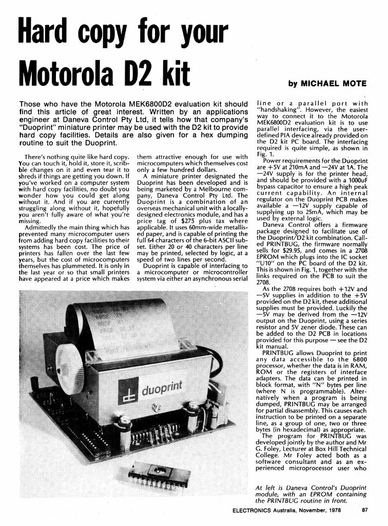
Those who have the Motorola MEK6800D2 evaluation kit should find this article of great interest. Written by an applications engineer at Daneva Control Pty Ltd, it tells how that company's "Duoprint" miniature printer may be used with the D2 kit to provide hard copy facilities. Details are also given for a hex dumping routine to suit the Duoprint.
There's nothing quite like hard copy. You can touch it, hold it, store it, scrib-ble changes on it and even tear it to shreds if things are getting you down. If you've worked on a computer system with hard copy facilities, no doubt you wonder how you could get along without it. And if you are currently struggling along without it, hopefully you aren't fully aware of what you're missing.
Admittedly the main thing which has prevented many microcomputer users from adding hard copy facilities to their systems has been cost. The price of printers has fallen over the last few years, but the cost of microcomputers themselves has plummeted. It is only in the last year or so that small printers have appeared at a price which makes
them attractive enough for use with microcomputers which themselves cost only a few hundred dollars.
A miniature printer designated the Duoprint has been developed and is being marketed by a Melbourne com-pany, Daneva Control Pty Ltd. The Duoprint is a combination of an overseas mechanical unit with a locally-designed electronics module, and has a price tag of $275 plus tax where applicable. It uses 60mm-wide metallis-ed paper, and is capable of printing the full 64 characters of the 6-bit ASCII sub-set. Either 20 or 40 characters per line may be printed, selected by logic, at a speed of two lines per second.
Duoprint is capable of interfacing to a microcomputer or microcontroller system via either an asynchronous serial
line or a parallel port with "handshaking". However, the easiest way to connect it to the Motorola MEK6800D2 evaluation kit is to use parallel interfacing, via the user-defined PIA device already provided on the D2 kit PC board. The interfacing required is quite simple, as shown in Fig. 1.
Power requirements for the Duoprint are +5V at 210mA and —24V at 1A. The —24V supply is for the printer head, and should be provided with a 1000uF bypass capacitor to ensure a high peak current capability. An internal regulator on the Duoprint PCB makes available a —12V supply capable of supplying up to 25mA, which may be used by external logic.
Daneva Control offers a firmware package designed to facilitate use of the Duoprint/D2 kit combination. Call-ed PRINTBUG, the firmware normally sells for $29.95, and comes in a 2708 EPROM which plugs into the IC socket "U10" on the PC board of the D2 kit. This is shown in Fig. 1, together with the links required on the PCB to suit the 2708.
As the 2708 requires both +12V and —5V supplies in addition to the +5V provided on the D2 kit, these additional supplies must be provided. Luckily the —5V may be derived from the —12V output on the Duoprint, using a series resistor and 5V zener diode. These can be added to the D2 PCB in locations provided for this purpose — see the D2 kit manual.
PRINTBUG allows Duoprint to print any data accessible to the 6800 processor, whether the data is in RAM, ROM or the registers of interface adapters. The data can be printed in block format, with "N" bytes per line (where N is programmable). Alter-natively when a program is being dumped, PRINTBUG may be arranged for partial disassembly. This causes each instruction to be printed on a separate line, as a group of one two or three bytes (in hexadecimal) as appropriate.
The program for PRINTBUG was developed jointly by the author and Mr G. Foley, Lecturer at Box Hill Technical College. Mr Foley acted both as a software consultant and as an ex-perienced microprocessor user who
At left is Daneva Control's Duoprint module, with an EPROM containing the PRINTBUG routine in front.
ELECTRONICS Australia, November, 1978
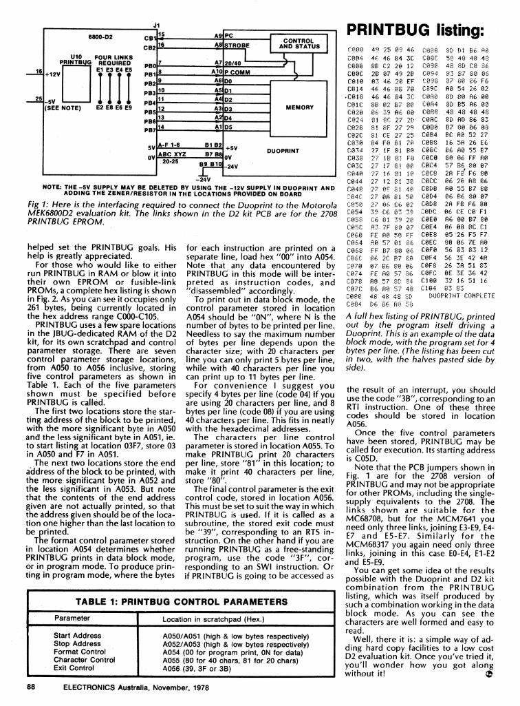
U10 FOUR LINKS PRINTBUG REQUIRED
El E3 E4 E5 +12V
-5V (SEE NOTE)
E2 E8 E6 E9
10 A5 D1 .. -
11 A4 D2 5 12 /2 D3 6 13 A D4
14 Al D5
MEMORY
J1 15
CB104,
CB2 16
16
25
A-F 1-6
20-25
helped set the PRINTBUG goals. His help is greatly appreciated.
For those who would like to either run PRINTBUG in RAM or blow it into their own EPROM or fusible-link PROMs, a complete hex listing is shown in Fig. 2. As you can see it occupies only 261 bytes, being currently located in the hex address range C000-C105.
PRINTBUG uses a few spare locations in the MUG-dedicated RAM of the D2 kit, for its own scratchpad and control parameter storage. There are seven control parameter storage locations, from A050 to A056 inclusive, storing five control parameters as shown in Table 1. Each of the five parameters shown must be specified before PRINTBUG is called.
The first two locations store the star-ting address of the block to be printed, with the more significant byte in A050 and the less significant byte in A051, ie. to• start listing at location 03F7, store 03 in A050 and F7 in A051.
The next two locations store the end address of the block to be printed, with the more significant byte in A052 and the less significant in A053. But note that the contents of the end address given are not actually printed, so that the address given should be of the loca-tion one higher than the last location to be printed.
The format controlparameter stored in location A054 determines whether PRINTBUG prints in data block mode, or in program mode. To produce prin-ting in program mode, where the bytes
PC CONTROL
AND STATUS
P COMM
DUOPRINT
for each instruction are printed on a separate line, load hex "00" into A054. Note that any data encountered by PRINTBUG in this mode will be inter-preted as instruction codes, and "disassembled" accordingly.
Toprint out in data bloCk mode, the control parameter stored in location A054 should be "ON", where N is the number of bytes to be printed per line. Needless to say the maximum number of bytes per line depends upon the character size; with 20 characters per line you can only print 5 bytes per line, while with 40 charactersper line you can print up to 11 bytes per line.
For convenience I suggest you specify 4 bytes per line (code 04) if you are using 20 characters per line, and 8 bytes per line (code 08) if you are using 40 characters per line. This fits in neatly with the hexadecimal addresses.
The characters per line control parameter is stored in location A055. To make PRINTBUG print 20 characters per line, store "81" in this location; to make it print 40 characters per line, store "80".
The final control parameter is the exit control code, stored in location A056. This must be set to suit the way in which PRINTBUG is used. If it is called as a subroutine, the stored exit code must be "39", corresponding to an RTS in-struction. On the other hand if you are running PRINTBUG as a free-standing program, use the code "3F", cor-responding to an SWI instruction. Or if PRINTBUG is going to be accessed as
PRINTBUG listing: 45 25 46 C,088 ;SD Di 86 58
roo4 4E 44 84 3C CO8C 58 48 48 42 C008 SE C2 25 12 C090 48 85 C8 34 COOC 28 07 49 28 ri-194 83 67 80 06 C010 03 4,; 20 EF CP98 R7 SO 06 F6 C014 46 46 88 70 CB9C 50 54 26 02 .0018 46 4A 84 3E CEiSS 8D 85 A6 00 CO1C 8B 02 87 80 C854 8D 85 56 00 CO20 06 39 A6 00 COPS .48 48 48 48 C0124 81 8C 27 2D CORC 8D AD 86 83 CO28 81 8F 27 29 CUES E7 88 04 08 CO2C 81 CE 27 25 C884 BC 50 52 27 C070 54 F5 81 7P. C888 16 55 26 E6 ro34 27. 1F 81 80 C58C 86 AO 55 87 C038 27 18 81 FO COCE1 80 06 FF 50
27 17 81 00 C5C4 57 34 85 07 0040 27 16 81 10 COCA: 25 FE F6 80 C044 27 12 Si 30 COCC 06 25 58 86 cR48 2 7 Si 40 CODO 50 55 87 80 CO4 C 27 OA 81•50 C8514 06 86 80 07 17 P50 27 06 C6 02 CSD8 2A F8 F6 80 ro54 39 C6 03 39 CODC 06 CE CO Fl
C 01 39 20 CSES 56 00 57 80 P3 7F 80 07 CSE4 06 08 SC Cl
CO6E1 FE AP 50 FF CSE8 05 *26 F5 F7 Rif 97 01 86 CSEC 80 06 7E 58
C068 FF 87 20 06 COFO 56 83 83 12 COAC 84 2C B7 80 COF4 54 3E 42 45 C070 07 84 80 04 COF8 26 35 51 83 C074 FE RO 57 36 CSFC OE
/ 3E 36 42
C078 55• 57 8D 24 0100 32 16 51 16 C 7c 86 50 57 48 C104 83 83 C080 48 48 48 2D DUOPRINT COMPLETE 0084 D4 84 50 7,3
A full hex listing of PRINTBUG, printed out by the program itself driving a Duoprint. This is an example of the data block mode, with the program set for 4 bytes per line. (The listing has been cut in two, with the halves pasted side by side).
the result of an interrupt, you should use the code "3B", corresponding to an RTI instruction. One of these three codes should be stored in location A056.
Once the' five control parameters have been stored, PRINTBUG may be called for execution. Its starting address is CO5D.
Note that the PCB jumpers shown in Fig. 1 are for the 2708 version of PRINTBUG and may not be appropriate for other PROMs, including the single-supply equivalents to the 2708. The links shown are suitable for the MC68708, but for the MCM7641 you need only three links, joining E3-E9, E4-E7 and E5-E7. Similarly for• the MCM68317 you again need only three links, joining in this case EO-E4, E1-E2 and E5-E9.
You can get some idea of the results possible with the Duoprint and D2 kit combination from the PRINTBUG listing, which was itself produced by such a combination working in the data block mode. As you can see the characters are well formed and easy to read.
Well, there it is: a simple way of ad-ding hard copy facilities to a low cost D2 evaluation kit. Onceyou've tried it, you'll wonder how you got along without it! 1.9
6800-D2
PB0 PB1
PB2
PB3
PB4
PB
PB PB7
B1 B2 5V +5V ABC XYZ B7 B OV OV
119 Bl° 24V -L
-24V NOTE: THE -5V SUPPLY MAY BE DELETED BY USING THE -12V SUPPLY IN DUOPRINT AND
ADDING THE ZENER/RESISTOR IN THE LOCATIONS PROVIDED ON BOARD
Fig 1: Here is the interfacing required to connect the Duoprint to the Motorola MEK6800D2 evaluation kit. The links shown in the D2 kit PCB are for the 2708 PRINTBUG EPROM.
8 9
A0.8
A7
A10
A61
A9
STROBE
20/40 1
TABLE 1: PRINTBUG CONTROL PARAMETERS
Parameter Location in scratchpad (Hex.)
Start Address A050/A051 (high & low bytes respectively) Stop Address A052/A053 (high & low bytes respectively) Format Control A054 (00 for program print, ON for data) Character Control A055 (80 for 40 chars, 81 for 20 chars) Exit Control A056 (39, 3F or 3B)
88 ELECTRONICS Australia, November, 1978

Microcomputer News & Products
New Motorola MEK6802D3 uses 6800 hardware and software and is greatly expandable
Choose a single board computer, add a suitable power supply and, perhaps, some additional external memory; put these into an enclosure and you have a complete microcomputer — ready to go to work.
Motorola have released their MOKEP range of low-cost, assembled and tested microcomputer products to enable people to do just that.
The MEK6802D3 microcomputer module is a single board with eight LED digits and hex keypad. Based on the MC6802 MPU/RAM/CLOCK chip and the MC6846 ROM/I0/TIMER chip, this module allows a user to easily evaluate and use Motorola's M6800 hardware and software. The module features a 2k byte Monitor (D3BUG), 256 bytes of user RAM and 128 bytes of stack, and is fully expandable with the other products in the MOKEP range via a 60-pin bus.
Memory requirements for EPROM/ROM or RAM can be satisfied through the inclusion of the three memory modules offered — the MEK68MM16 16k byte dynamic memory, the MEK68MM32 32k byte dynamic memory or the MEK68RR ROM and RAM board. The latter accepts up to 8k bytes of static RAM
and up to 32k bytes of EPROM or 64k bytes of ROM. The MEK6802D3 has memory paging circuitry giving an ex-pansion capability to 160k bytes of ROM and 256k bytes of RAM.
Owners of the ever popular MEK6800D2 kits have not been forgotten. Each of the above-
mentioned boards has a counter-part compatible for use with the D2.
Further information about these products is available from Total Elec-tronics: Melbourne, (03) 596 2891; Sydney (02) 428 3500; Brisbane (07) 52 4357.
Micronews Continued
86 ELECTRONICS Australia, January, 1980

TV INTERFACE MODULE MEK68R2M, used with the D3 and Motherboard — a typical small system.
1)3, THE NEW LOW COST POWER BASE
TO BUILD YOUR SYSTEM ON!
Motorola's Microcomputer Expansion Systems are built around the completely new D3 module, and that means you now get all the versatility you want on one printed circuit board. This new module is the power base on which you can build your own powerful micro system, and it's big capacity allows
you to construct simple or complex systems — as you want them.
D3 features a multilevel memory paging technique, memory expandable to 256 K bytes RAM, and 160 K bytes ROM, a 2 K byte monitor — D3 BUG, for control of the systems microprocessor through the D3 hexadecimal keypad and LED display.
And there's the 16 K byte dynamic memory module, a television interface board, the combination card cage
and motherboard, wirewrap board, and a RAM/ROM board. No assembly or soldering because Motorola have designed each module to simply plug into the motherboard and the D3 module does the rest ! If you have one of the ever popular D2 kits — don't panic. There is a new range of expansion products to suit these kits too!
84 ELECTRONICS Australia, March, 1980

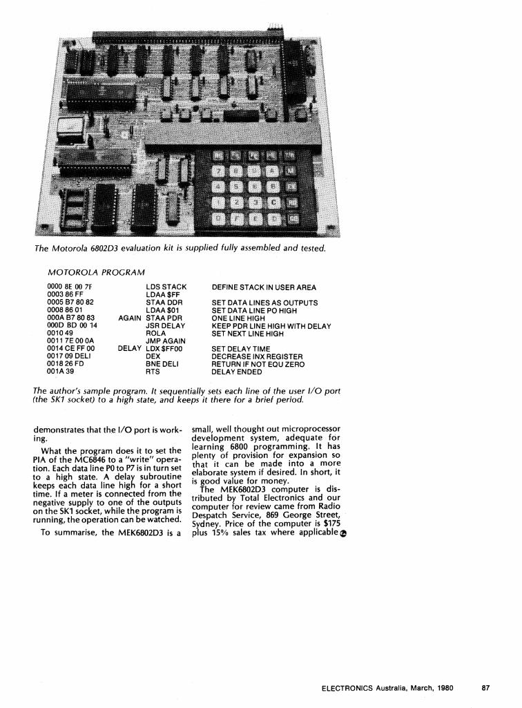
Motorola 61302D3 evaluation kit
Features a hexadecimal keyboard and LED readout
As recently announced, Motorola has just released a new microprocessor evaluation kit based on the MC6802. Called the MEK6802D3, the new system is supplied fully assembled and supersedes the well known MEK6800D2 two-board evaluation kit. The MEK6802D3 is accommodated on a single PCB which has a hexadecimal keyboard and an eight-digit LED readout.
Many of our readers will probably be sorry to see the end of the Motorola MEK6800D2 but they may rest assured that most of its features are carried on in the newly released MEK6802D3 system.
The single board D3 system employs the MC6802 microprocessor chip which has all the registers and accumulators of the MC6800 plus an internal clock os-cillator and driver. In addition, the 6802 has 128 bytes of RAM and a "Vcc stand-by" feature which allows the first 32 bytes of RAM memory to be retained in a low power mode.
In addition to the MC6802 chip ther are two MC6810 static RAMs, orie MC6821 Peripheral Interface Adaptor (PIA) and MC6846 ROM-I/O-Timer'. A 3.579545MHz crystal reference is provided for the clock. This frequency is divided by four within the MC6802 chip itself which consequently operates on 894.88k Hz.
The MC6821 PIA is provided for in-terfacing the keyboard and LED dis-plays to the processor. The only user in-put/output clevice is the relatively new chip, the MC6846. The MC6846 provides 2048 8-bit bytes of ROM, an 8-bit bidirectional dataport for parallel interface plus two control lines and programmable interval timer-counter functions. The ROM accommodates the D3BUG monitor program. The data port differs from a standard PIA in that all the control registers can be accessed so that, for example, the choice of positive or negative edge triggering and/or latching can be easily im plemented.
The timer within the MC6846 can be operated in various modes such as pulse width comparison, frequency comparison, normal single-shot con-
tinuous and cascaded single-shot operations. Comprehensive i nforma-tion isgiven on all these modes in the data sheets.
The total volatile memory (RAM) available on the D3 computer board is 256 bytes.
The D3 evaluation kit is supplied fully assembled and tested. All that is need-ed to have it running is a 5V power supply capable of delivering 900 milliamps. Dimensions of the double-sided PCB are 210 x 180mm.
Comprehensive literature is provided in loose-leaf form, suitable for insertion into a standard 3-ring binder. The literature includes a manual on the D3 system itself, with chapters on general description and operation, hardware, software and expansion. Data sheets on all the major chips in the D3 system are provided plus schematics and an appendix on number systems and 6800 addressing modes. Also supplied is a programming reference manual on the M6800.
The D3BUG monitor is quite an ad-vance on the JBUG monitor program of the D2 kit. With the D2, memory could only be advanced when in JBUG, however, with the D3BUG memory can be also stepped backwards. Breakpoints with the D3 computer can be removed separately, whereas the D2 monitor only removed breakpoints all at once. Up to eight breakpoints can be inserted compared to the D2's five.
Using breakpoints is easy with the D3BUG since the registers and their contents are displayed. The D3BUG will also calculate offsets for branch instruc-tions. Just enter the start address, type the "FS" key and enter the final ad-dress. Type "GO" and the hexadecimal offset is displayed. The D2 kit had a
by JOHN CLARKE
separate program to calculate offsets. The D3 computer as it stands is not
capable of transferring RAM contents onto an audio tape, although there is routine in the D3BUG monitor program. An extra board is required to be connected to the D3system bus to enable use of the dump and load routine.
A chapter in the manual is devoted to expansion of the D3 computer. This chapter is well written and describes the necessary modifications required for the expansion boards. Extra memory boards and a colour TV monitor interface board are examples of the variety of expansion boards available.
Working through the introductory program load-run-debug example which Motorola have thoughtfully provided in the kit manual, I quickly learned to operate the system in D3BUG. The example is well done and should be equally effective in in-troducing a newcomer to microprocessing systems.
Programming the system was more difficult until I was able to sort out the addressing modes. Once this was done, another problem arose; how to access the I/O peripheral port? The manual refers to the PIA timer address being located Pat 8080 to 8087 but the order in which the registers are located is not clear. Reference to the data sheets showed a truth table for the register selection.
After conversion of the addresses 8080 to 8087, it became clear that the registers are located in memory in the order in which they occur in the above truth table. With that sorted out I was able to write a short program which
86 ELECTRONICS Australia, March, 1980
••••:••••,•••
•
The Motorola 6802D3 evaluation kit is supplied fully assembled and tested.
MOTOROLA PROGRAM
0000 8E 00 7F LDS STACK DEFINE STACK IN USER AREA 0003 86 FF LDAA $FF 0005 B7 80 82 STAA DDR SET DATA LINES AS OUTPUTS 0008 86 01 LDAA $01 SET DATA LINE PO HIGH 000A B7 80 83 AGAIN STAA PDR ONE LINE HIGH 000D BD 00 14 JSR DELAY KEEP PDR LINE HIGH WITH DELAY 0010 49 ROLA SET NEXT LINE HIGH 0011 7E 00 OA JMP AGAIN 0014 CE FF 00 DELAY LDX $FFOO SET DELAY TIME 0017 09 DELI DEX DECREASE INX REGISTER 0018 26 FD BNE DELI RETURN IF NOT EQU ZERO 001A 39 RTS DELAY ENDED
The author's sample program. It sequentially sets each line of the user I/O port (the SK1 socket) to a high state, and keeps it there for a brief period.
demonstrates that the I/O port is work-ing.
What the program does it to set the PIA of the MC6846 to a "write" opera-tion. Each data line PO to P7 is in turn set to a high state. A delay subroutine keeps each data line high for a short time. If a meter is connected from the negative supply to one of the outputs on the SK1 socket, while the program is running, the operation can be watched.
To summarise, the MEK6802D3 is a
small, well thought out microprocessor development system, adequate for learning 6800 programming. It has plenty of provision for expansion so that it can be made into a more elaborate system if desired. In short, it is good value for money.
The MEK6802D3 computer is dis-tributed by Total Electronics and our computer for review came from Radio Despatch Service, 869 George Street, Sydney. Price of the computer is $175 plus 15% sales tax where applicable a
ELECTRONICS Australia, March, 1980 87
ANNOUNCING
DEVELOPMENT SYSTEMS The EXORmacs Development System for 68000 has just been announced. The system includes 15 slot chassis and power supply, MPU module, memory management module, deBUG module, 128K byte dynamic memory module, and an intelligent floppy disk controller module.
Software includes Structured Macro Assembler/Linkage Editor, screen based editor, symbolic deBUG and a PASCAL compiler.
Peripherals include intelligent CRT console, a 1 Mbyte, two drive double sided floppy disk, and a model 703 (180 CPS 132 column) line printer.
A large number of support modules are also available.
6800/6809 EXORciser Development Systems The popular EXORciser ri Development System is now available in both 6800 and 6809 versions. For those people already owning a 6800 EXORciser or EXORterm Development System, a 6809 upgrade kit is available. Both EXORcisers may be expanded to allow development of the
MC6802 / MC6808 MC6801/MC6803/MC68701 MC6805 A wide range of support modules are
available, including support modules for PIA, ACIA, SSDA, ADLC, GPIA, CRT controller and universal support module.
High level languages are available for - 6800: BASIC, FORTRAN, COBOL, MPL. 6809: FORTRAN, MPL, PASCAL.
Bulk storage is available on both single and double sided floppy disks. Up to 4 drives are supported.
A 10 Mbyte Hard Disk System is also available with expansion to 40 Mbyte. The Hard Disk System may co-reside with the floppy system to allow easy transfer of old files.
68000 Courses Rank Electronics has much pleasure in announcing a visit from two leading Motorola lecturers to give courses on the MC68000.
Subjects will include both hardware and software aspects.
Course costs: $250.00 per head for each course.
Dates: Sydney — May 19, 20, 21 and 22. Brisbane — May 23, 26 and 27. Adelaide — May 28, 29 and 30. Melbourne — June 2, 3, 4 and 5.
Hours: Sydney and Melbourne — 9.00 a.m. to 5.00 p.m. Brisbane and Adelaide — 8.30 a.m. to 7.30 p.m.
For further details and application form please contact:
RANK ELECTRONICS PTY LIMITED INDUSTRIAL SYSTEMS
12 Barcoo Street, East Roseville, Sydney 2069. Phone 406 5666 60 Rosebank Ave, Clayton South, Vic 3169 Telephone 541 8444 299 Montague Road, West End, Brisbane 4101. Telephone 44 2851 101-105 Mooringe Avenue, Camden Park, SA 5038. Telephone 294 6555 430 Newcastle Street, Perth 6000. Phone 328 3933 120 Parry Street, Newcastle 2300. Phone 26 2466 MAS5561
30 ELECTRONICS Australia, April, 1980

•
Break away from he past.
C
Motorola's MC68000 sets new MPU system performance standards for the '80s. Now. Motorola announces a new microprocessor so advanced in concept it offers the design& virtually unlimited freedom of system design. Advanced technologies provide it with a speed/power product four times that of standard NMOS. Break away from the past and step into the new era of microprocessors.
Everything you need for system design is available now—a Design Module for evaluating the MC68000, development hardware and software, full documentation and training. In addition, the MC68000 interfaces directly and easily with existing M6800 Family peripherals, MPUs, and MCUs.
The MC68000 is, by design, perfect for an easy-to-handle, block-structured, high-level language like PASCAL. It simplifies modern programming techniques like modular programming. Complete M68000 design support available now. Concurrent with introduction of the MC68000, the design tools to help you break away from the past are now available.
A major commitment to development of timely and effective M68000 hardware and software has been part of the program from the beginning. The results, part innovation and part evolution, give you a choice among Motorola's EXORciser®, the
IBM 370 and the PDP*-11 for system hardware and software development. Motorola offers the total range of microcomponents for your advanced systems. Motorola's original M6800 Family pioneered the concept of the fully-compatible, matched set microprocessor plus I/O, peripheral controller and memory family, complete with support hardware, software and training.
The MC68000 springs from a rich tradition in both microcomponents and MOS technology and is designed to develop in the same total family way as the M6800 Family.
Pace-setting products like the MCM6664 64K dynamic RAM, the MC6809 super 8-bit microprocessor, and the definitive MC6801 and M6805 Family one-chip MCUs have firmly established Motorola's capability. For further details and application form please contact:
RANK ELECTRONICS PTY LIMITED INDUSTRIAL SYSTEMS
12 Barcoo Street, East Roseville NSW 2069. Phone: 406 5666 60 Rosebank Avenue, Clayton South Vic 3169. Phone: 541 8444 299 Montague Road, West End, Brisbane 4101. Phone 44 2851 101-105 Mooringe Avenue, Camden Park SA 5038. Phone 294 6555 430 Newcastle Street, Perth WA 6000. Phone: 328 3933 120 Parry Street, Newcastle NSW 2300. Phone: 26 2466
*Trademark of Digital Equipment Corporation. MAS5694
ELECTRONICS Australia, June, 1980
17

' '
Microcomputer News [!] ! I '
/ ./;(Jl!<""f/ ,I ,: '""'"·:W.
._______ __ ---·-
Motorola evaluation board for the MC68000 Motorola Inc has released an evaluation board for the MC68000 1 6-bit microprocessor. For those interested in exploring the capabilities of this chip the MEX68KECB (Educational Computer Board) provides a (relatively) low cost 68000 system, needing only a power supply and a serial terminal.
Intended primarily for training and educational use, the Educational Computer Board serves as a comprehensive introduction to systems based on the 68000 microprocessor. The board measures just 264 x 168mm yet provides everything necessary to begin writing and testing machine language programs for the MC68000 16-bit microprocessor.
On the board are a MC68000 processor running at 4MHz, 32K bytes of
selected by jumper blocks and may be any standard rate between 11 0 and 9600 baud.
So that the ECB can be used immediately, extensive software is included in ROM on the board. Called "Tutor", this software provides the user with a monitor and debugging package, assembler and disassembler and 1/0 control functions.
The MC68000 microprocessor is often
The MEX68KECB board provides 32K of RAM, parallel and serial ports and software.
dynamic RAM arranged as 16K x 16 bit ·, words, two RS232C serial communica
tions ports, a 16-bit parallel input/output port (which can be configured as a Centronics compatible printer port), a cassette tape interface for program
· storage, a 24-bit programmable timer and Reset and Abort pushbutton switches.
For those wishing to add their own interface circuits a small prototyping area is also provided.
The user must add power supplies of ±1V and ±12V, and a serial terminal. Communications rates for the board are
referred to as a 16/32 bit microprocessor, as it has a 16-bit external data bus but internally is organised around 32-bit registers. In addition to a 32-bit program counter and 16-bit status register, the processor provides 17 32-bit registers. Of these, the first eight may be used for byte, word or "long word" (32-bit) storage while the second group of eight and the 32-bit stack pointer can be used as address registers, for word and long word manipulation and as index registers.
The external address bus is 24-bits wide, providing a direct addressing
128 ELECTRONICS Australia, April, 1983
range of 16 megabytes (16,777,216 bytes). A CHK (Check register against bounds) instruction allows the programmer to create a variety of memory protection/management routines.
Other features of the processor are the ease of single step debugging provided by a trace mode called up by the instruction "TRAP". The processor also makes a distinction between two modes of operation, the "user" and "supervisor" states. The user mode prohibits access to certain of the memory instructions, allowing programs for multi-user systems to be written in such a way so that they will not interfere with each other even in the event of an error.
The 16K "Tutor" software provided with the Educational Computer Board is basically a system monitor which controls communication with the terminal and· allows the creation and testing of assembly language programs. The lineby-line assembler does not save the source program but translates each instruction into the correct machine code for storage in memory. Facilities are limited to the specification of operation and operands- line numbers, labels and comments are not allowed.
_· The disassembler also operates on a line-by-line basis, disassembling the machine code in memory and displaying the instruction mnemonic and operands. Jli4o editing facilities are provided other t~ re-entering the source statement. For;:other facilities a macro assembler or cross assembler can be run on a host computer, with data communicated to the 68000 board through the second serial port.
In addition to the assembler/disassembler, Tutor provides com-, mands to display and modify memory and registers, commands for executing programs, either continuously or with breakpoints, or in a Trace mode. Other commands allow blocks of memory to be filled, moved or searched for a specified character and there are also commands for controlling the serial communications ports and parallel printer inter.face and for dumping and loading programs from a cassette recorder.
Documentation provided with the board consists of a 200-page loose leaf manual which covers the set up and