Micro and nano patterning of carbon electrodes for bioMEMS · PDF fileBioinspired, Biomimetic...
14
Bioinspired, Biomimetic and Nanobiomaterials Volume 1 Issue BBN4 Micro and nano patterning of carbon electrodes for bioMEMS Sharma and Madou 252 ice | science 1. Introduction In recent years, carbon has received much attention as a material for micro and nanofabrication. Rigorous research has been performed on carbon nanotubes (CNTs), carbon microelectromechanical systems (CMEMS), carbon nanomechanical systems (CNEMS), carbon micro/nanofibers, carbon nanospheres, carbon whiskers, and graphene for applications in biomedical engineering, sensor technology, and electronic applications. 1–5 Initially, silicon was employed as the platform of choice for most MEMS fabrication because fabrication methodologies and equipment from the integrated circuit industry, which operates almost exclusively on silicon, could be adapted. 6 In those early days, the mid-80s, MEMS applications were limited to pressure sensors, accelerometers, and gyros, for which Si is an excellent material’s choice. With MEMS being applied more and more to biomedical applications, ‘bioMEMS’ evolved, representing a new class of MEMS that commands its own fabrication tools and involves a much wider range of materials. BioMEMS devices include biosensors such as glucose sensors blood gas blood electrolyte sensors, lab-on-chip systems and diagnostic medical tools such as protein and DNA arrays. 6 Because of the irreversible chemical reactions involved in many medical tests (e.g. nucleic acid and immuno assays) and because of contamination considerations, bioMEMS devices tend to be disposable, and therefore call for an inexpensive material and fabrication technique. Today, biocompatible metals (e.g. silver, gold), 7,8 various biodegradable polymers (e.g. polycaprolactone), 9 soft-biocompatible polymers such as silicone (polydimethylsiloxane (PDMS)) 10 and advanced carbon materials (CMEMS, CNEMS, carbon fibers (CFs) and capsules, CNTs, etc.) 1–5,11 often replace silicon for disposable bioMEMS applications. Carbon, in particular, is a low-cost material that can be derived by the carbonization of certain precursor polymers. Also, CMEMS/ CNEMS fabrication processes are suitable for mass manufacturing and that makes them attractive for a wide-variety of future bioMEMS applications. CMEMS and CNEMS applications employ micro and nanodevices of a wide-variety of shapes, dimensions, and chemical and mechanical properties that are otherwise difficult or very expensive to implement. 12 With advanced photolithographic techniques and the use of appropriate precursor polymer materials such as SU8, fabrication of miniaturized carbon devices has rapidly evolved from the micrometer-sized CMEMS devices to nanometer-sized CNEMS devices. 12 Today, the most common fabrication methodology for CMEMS and CNEMS fabrication is photolithography of a photoresist (mainly SU8), and carbonization of the thus patterned polymer by pyrolysis. 2,11,12 Some of the early attempts of CMEMS fabrication also employed patterning by soft lithography, 13 molding, 14,15 and chemical vapor deposition. 16 Here, the fabrication Micro and nano patterning of carbon electrodes for bioMEMS Swati Sharma* MSc PhD Student, Materials and Manufacturing Technology, University of California, Irvine (UCI), California, USA Marc Madou PhD Chancellor’s Professor, Mechanical & Aerospace Engineering and Biomedical Engineering, University of California, Irvine (UCI), California, USA Carbon based bioMEMS are an emerging class of miniaturized biomedical devices. Due to the numerous advantages such as scalable manufacturing processes, inexpensive and readily available precursor polymer materials, tunable surface properties and biocompatibility, carbon has become a preferred material for a wide variety of future biosensing applications. In this article, we review fabrication methodologies for carbon-MEMS (CMEMS) and carbon-NEMS (CNEMS) devices and strategies for their surface modification for biocompatibility and for biosensing. We also discuss the underlying graphitic and glassy microstructures of carbon since the biocompatibility of carbon and its microstructures are intertwined. We conclude by exploring various CMEMS and CNEMS devices that have been successfully fabricated. 1 2 Pages 252–265 http://dx.doi.org/10.1680/bbn.12.00010 Themed Issue Paper Received 07/05/2012 Accepted 12/06/2012 Published online 27/06/2012 Keywords: carbon MEMS/bioMEMS/biosensor ICE Publishing: All rights reserved 1 2 *Corresponding author email address: [email protected]
Transcript of Micro and nano patterning of carbon electrodes for bioMEMS · PDF fileBioinspired, Biomimetic...

Bioinspired, Biomimetic and NanobiomaterialsVolume 1 Issue BBN4
Micro and nano patterning of carbon electrodes for bioMEMSSharma and Madou
252
ice | science
1. IntroductionIn recent years, carbon has received much attention as a material for
micro and nanofabrication. Rigorous research has been performed on
carbon nanotubes (CNTs), carbon microelectromechanical systems
(CMEMS), carbon nanomechanical systems (CNEMS), carbon
micro/nanofi bers, carbon nanospheres, carbon whiskers, and graphene
for applications in biomedical engineering, sensor technology, and
electronic applications.1–5 Initially, silicon was employed as the
platform of choice for most MEMS fabrication because fabrication
methodologies and equipment from the integrated circuit industry,
which operates almost exclusively on silicon, could be adapted.6
In those early days, the mid-80s, MEMS applications were limited
to pressure sensors, accelerometers, and gyros, for which Si is an
excellent material’s choice. With MEMS being applied more and
more to biomedical applications, ‘bioMEMS’ evolved, representing
a new class of MEMS that commands its own fabrication tools
and involves a much wider range of materials. BioMEMS devices
include biosensors such as glucose sensors blood gas blood
electrolyte sensors, lab-on-chip systems and diagnostic medical
tools such as protein and DNA arrays.6 Because of the irreversible
chemical reactions involved in many medical tests (e.g. nucleic acid
and immuno assays) and because of contamination considerations,
bioMEMS devices tend to be disposable, and therefore call for an
inexpensive material and fabrication technique. Today, biocompatible
metals (e.g. silver, gold),7,8 various biodegradable polymers (e.g.
polycaprolactone),9 soft-biocompatible polymers such as silicone
(polydimethylsiloxane (PDMS))10 and advanced carbon materials
(CMEMS, CNEMS, carbon fi bers (CFs) and capsules, CNTs,
etc.)1–5,11 often replace silicon for disposable bioMEMS applications.
Carbon, in particular, is a low-cost material that can be derived by
the carbonization of certain precursor polymers. Also, CMEMS/
CNEMS fabrication processes are suitable for mass manufacturing
and that makes them attractive for a wide-variety of future bioMEMS
applications. CMEMS and CNEMS applications employ micro and
nanodevices of a wide-variety of shapes, dimensions, and chemical
and mechanical properties that are otherwise diffi cult or very
expensive to implement.12
With advanced photolithographic techniques and the use of
appropriate precursor polymer materials such as SU8, fabrication
of miniaturized carbon devices has rapidly evolved from the
micrometer-sized CMEMS devices to nanometer-sized CNEMS
devices.12 Today, the most common fabrication methodology
for CMEMS and CNEMS fabrication is photolithography of a
photoresist (mainly SU8), and carbonization of the thus patterned
polymer by pyrolysis.2,11,12 Some of the early attempts of CMEMS
fabrication also employed patterning by soft lithography,13
molding,14,15 and chemical vapor deposition.16 Here, the fabrication
Micro and nano patterning of carbon electrodes for bioMEMS
Swati Sharma* MScPhD Student, Materials and Manufacturing Technology, University of California, Irvine (UCI), California, USA
Marc Madou PhDChancellor’s Professor, Mechanical & Aerospace Engineering and Biomedical Engineering, University of California, Irvine (UCI), California, USA
Carbon based bioMEMS are an emerging class of miniaturized biomedical devices. Due to the numerous advantages
such as scalable manufacturing processes, inexpensive and readily available precursor polymer materials, tunable surface
properties and biocompatibility, carbon has become a preferred material for a wide variety of future biosensing applications.
In this article, we review fabrication methodologies for carbon-MEMS (CMEMS) and carbon-NEMS (CNEMS) devices and
strategies for their surface modifi cation for biocompatibility and for biosensing. We also discuss the underlying graphitic
and glassy microstructures of carbon since the biocompatibility of carbon and its microstructures are intertwined. We
conclude by exploring various CMEMS and CNEMS devices that have been successfully fabricated.
1 2
Pages 252–265 http://dx.doi.org/10.1680/bbn.12.00010Themed Issue PaperReceived 07/05/2012 Accepted 12/06/2012Published online 27/06/2012Keywords: carbon MEMS/bioMEMS/biosensor
ICE Publishing: All rights reserved
1 2
*Corresponding author email address: [email protected]

Bioinspired, Biomimetic and NanobiomaterialsVolume 1 Issue BBN4
Micro and nano patterning of carbon electrodes for bioMEMSSharma and Madou
253
process for CMEMS/CNEMS with representative examples from
both SU8 and non-SU8 based techniques is described.
The most desirable feature of carbon-based bioMEMS devices is the
amenability to surface modifi cation of carbon. Carbon is easier to
derivatize with organic molecules compared to most other traditional
MEMS materials such as silicon. Carbon surface modifi cation
can entail chemical and electrochemical modifi cation17–19 as well
as topographical changes.20 In this context, it is important to
understand the underlying microstructure of the various allotropes
of carbon, since the carbon surface refl ects its internal molecular
arrangements.21 Carbon microstructures are usually determined
by the fabrication process details and by the choice of polymer
precursor. In this study, glassy carbon (GC) designs are mostly
dealt since GC is the most commonly used material for bioMEMS
applications. However, in order to better understand the surface
modifi cation techniques and the thus resulting biocompatibility,
examples of carbon micro and nanofi bers that often feature a more
graphitic microstructure are also reviewed. CFs, so far, have not
been implemented for bioMEMS purposes; nevertheless, they have
been successfully employed as implant materials.
2. Carbon microstructureThe properties of carbon vary widely as it comes in many different
allotropes based on the fabrication method involved. CNTs,
graphene, carbon whiskers, and carbon nanofi bers (CNFs) are
non-glassy materials, whereas carbon obtained from pyrolysis of
a precursor polymer is usually glassy (GC). The microstructure of
GC is surprisingly dissimilar from the other carbon allotropes of
carbon and its exact nature has been a matter of dispute for many
years.22–24 GC exhibits excellent electrochemical properties and
may substitute more expensive noble metals such as Pt and Au
commonly employed for the fabrication of miniaturized sensing
electrodes.25–27 For electrochemists, GC electrodes are often used as
the gold standard to compare the electrochemical behavior of other
electrodes. Using CMEMS and CNEMS technology, very small GC
electrode designs are possible by lithographic patterning a photoresist
and carbonizing the design, resulting in sensing devices with novel
geometries and unprecedented sensitivities.28 The fabrication cost of
sophisticated carbon electrode designs is small compared with that
of the more involved patterning of noble metal electrodes because
of the simplicity and the wide range of polymer precursors that are
available in CMEMS and CNEMS processing11 (see Section 3).
In most cases, upon pyrolysis of polymer precursors, a GC results that
possesses glass-like properties and shatters upon breaking. Carbon
is one of the few materials that tends to polymerize with itself,
and therefore, when a precursor polymer is heated to temperatures
high enough to remove more volatile elements, new C-C bonds are
formed. This self-polymerization leads to a network of carbon, the
molecular structure of which depends upon several factors including
the nature and chemical structure of the polymer precursor,
fabrication methodology, pyrolysis temperature, mechanical and
electrical forces acting on the precursor polymer chains, etc.12 These
tunable factors may enhance graphitization especially in the case of
polymer derived CNFs as discussed in detail in Sharma et al.12 More
typically, though bulk polymers with high carbon content such as
SU8, polyacrylonitrile (PAN), polyimides, and polyimides yield GC
upon pyrolysis between 800 and 1200°C. CMEMS fabricated using
photolithography of SU8 have attracted much attention in the recent
past because of their compatibility with deep UV photolithography,
high carbon yield of SU8, and a wide variety of high-aspect-ratio
micro/nano designs (see Section 5).
The exact microstructure of GC was a controversial topic among
researchers for a long time because of the uncertainty of the nature
of the prevailing intermolecular cross-links. As far back as 1951,
Rosalind Franklin23 carried out a comparative study employing
X-ray crystallography to investigate the amount of crystallinity in
graphitizing and non-graphitizing carbons. According to Franklin,
a graphitizing carbon is one that gets converted completely to
graphite upon heat treatment whereas a non-graphitizing carbon is
amorphous or glassy in nature and cannot be converted completely
to graphite even at very high pyrolysis temperatures. Jenkins and
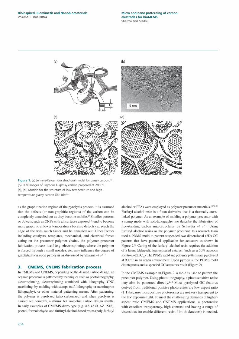
Kawamura22 proposed a model for the structure of GC that consists
of a ribbon-like geometry of entangled carbon sheets (Figure
1(a)). Franklin’s and Jenkins et al’s initial observations were made
analyzing X-ray diffraction patterns, using more advanced structural
analysis techniques, such as high-resolution transmission electron
microscopy (HRTEM). It became evident that even non-graphitizing
polymer derived carbons do contain small isolated crystals of
graphite. These graphitic regions, however, may not fully develop
into full graphite sheets because of chain morphology restrictions in
the parent polymer structure and space constrains. Harris24 proposed
a structural model for non-graphitizing carbons based on HRTEM
imaging, and ventured that GC only contains sp2-hybridized carbons
such as those found in fullerenes. These sp2-bonded carbons contain
six-membered rings as well as fi ve and seven membered rings, and
are highly stable. This model is supported by HRTEM images of
commercially available GC (Figure 1(b)). Harris suggested that GC
prepared at different temperatures results in different packing of the
dispersed carbon sheets (Figures 1(c) and 1(d)).
To better understand the microstructure carbon may adopt while it
evolves from its polymer precursor, it is of paramount interest to
discuss the chemical changes that take place during the pyrolysis
process. When a polymer pattern is pyrolyzed, a multi-step
carbonization process takes place.29 Initially, in the 300–500°C
temperature range, called the carbonization regime, there is a rapid
polymer weight loss because of the removal of elements such as
oxygen, nitrogen, chlorine, etc. Above 500°C, hydrogen attached
to carbon atoms is cleaved off and removed. A high purity GC,
that is, one with almost all H atoms removed, is usually obtained
between 800–1200°C. If the temperature is further increased,
graphitic zones start to form. Between 2500 and 3300°C, known
Bioinspired, Biomimetic and NanobiomaterialsVolume 1 Issue BBN4
Micro and nano patterning of carbon electrodes for bioMEMSSharma and Madou
254
as the graphitization regime of the pyrolysis process, it is assumed
that the defects (or non-graphitic regions) of the carbon can be
completely annealed out as they become mobile.29 Smaller patterns
or objects, such as CNFs with all surfaces exposed12 tend to become
more graphitic at lower temperatures because defects can reach the
edge of the wire much faster and be annealed out. Other factors
including catalysts, templates, mechanical, and electrical forces
acting on the precursor polymer chains, the polymer precursor
fabrication process itself (e.g. electrospinning, where the polymer
is forced through a small nozzle), etc. may infl uence the degree of
graphitization upon pyrolysis as discussed by Sharma et al.12
3. CMEMS, CNEMS fabrication processIn CMEMS and CNEMS, depending on the desired carbon design, an
organic precursor is patterned by techniques such as photolithography,
electrospinning, electrospinning combined with lithography, CNC
machining, by molding with stamps (soft-lithography or nanoimprint
lithography), or other material patterning means. After patterning,
the polymer is pyrolyzed (also carbonized) and when pyrolysis is
carried out correctly, a shrunk but isometric carbon design results.
In early examples of CMEMS diazo type (e.g. AZ 4330, AZ 1518),
phenol-formaldehyde, and furfuryl alcohol-based resins (poly-furfulyl
alcohol or PFA) were employed as polymer precursor materials.13,30,31
Furfuryl alcohol resin is a furan derivative that is a thermally cross-
linked polymer. As an example of molding a polymer precursor with
a stamp made with soft-lithography, we describe the fabrication of
free-standing carbon microstructures by Schueller et al.13 Using
furfuryl alcohol resins as the polymer precursor, this research team
used a PDMS mold to pattern suspended two-dimensional (2D) GC
patterns that have potential application for actuators as shown in
Figure 2.13 Curing of the furfuryl alcohol resin requires the addition
of a latent (delayed), heat-activated catalyst (such as a 50% aqueous
solution of ZnCl2). The PDMS mold and polymer patterns are pyrolyzed
at 900°C in an argon environment. Upon pyrolysis, the PDMS mold
disintegrates and suspended GC actuators result (Figure 2).
In the CMEMS example in Figure 2, a mold is used to pattern the
precursor polymer. Using photolithography, a photosensitive resist
may also be patterned directly.2,12 Most pyrolysed GC features
derived from traditional positive photoresists are low aspect ratio
(1:1) because most positive photoresists are not very transparent to
the UV exposure light. To meet the challenging demands of higher-
aspect ratio CMEMS and CNEMS applications, a photoresist
with excellent transparency, high contrast and having a range of
viscosities (to enable different resist fi lm thicknesses) is needed.
Figure 1. (a) Jenkins-Kawamura structural model for glassy carbon.22
(b) TEM images of Sigradur G glassy carbon prepared at 2800oC.
(c), (d)) Models for the structure of low-temperature and high-
temperature glassy carbon ((b)–(d)).24
Lc
La
(a)
(c) (d)
(b)
5 nm

Bioinspired, Biomimetic and NanobiomaterialsVolume 1 Issue BBN4
Micro and nano patterning of carbon electrodes for bioMEMSSharma and Madou
255
An epoxy novolac-based negative photoresist, SU8, developed by
IBM and marketed by MicroChem Inc., Newton, MA, USA and
Gersteltec SARL, Pully, Switzerland,32,33 meets these requirements
as it has a very high deep UV transparency, good contrast in the
near UV range (350–400 nm) and is available in a wide range of
viscosities.11,33 Unlike some other negative tone photoresists,34
SU8 does not exhibit any oxygen sensitivity, which may lower the
fabrication speed and/or lead to pattern distortions.
The standard procedure for fabrication of high-aspect-ratio
CMEMS (carbon posts in this case) or CNEMS employing SU8 is
illustrated in Figure 3.
SU8 formulation with the optimal viscosity for the intended
application is fi rst spin coated on the desired substrate (Figure
3(a)). Before spin coating, the substrate must be cleaned thoroughly
and depending on the requirement of the process, an adhesive (e.g.
OmniCoat, MicroChem Inc.) may be used before spinning or
casting SU8 on it. In the case of spin coating, the rotation speed
of the spin coater, the resist viscosity, and resist concentration
control the resulting resist thicknesses. The prebake (also soft
bake or preexposure bake) step of the SU8 fi lm thus coated on a
substrate consists of fi rst heating the sample to 65°C and then to
95°C in order to evaporate the solvent slowly. If the fi lm is exposed
to a very high temperature too abruptly (for example, because
of a false reading of the hot plate temperature), the evaporation
of solvent will not be uniform and some solvent may remain
trapped, especially in the case of thicker fi lms. The UV exposure
(Figure 3(b)) is the crucial step in any photoresist patterning
process. During exposure, prebaked SU8 is exposed to UV light
through a mask that is aligned with the substrate in a mask aligner.
The energy supplied by the UV light initiates cross-linking by
activating the photo-initiators present in the SU8 photoresist. The
required exposure dose can be calculated from the commercially
available SU8 data sheets.33 Establishing the correct UV dose for a
given SU8 fi lm is of the utmost importance since both under- and
Figure 2. Scanning electron micrographs of GC structures prepared by
carbonization at 1000°C of furfulyl alcohol resin. (a) and (b) The inner
frame can be electrostatically actuated. This type of structure represents
the sensing unit for an accelerometer. (c) Precursor to an interdigitated
capacitor. The interdigitated comb structures become electrically
isolated once the supporting frame is broken. (d) Optical defl ector. The
initial carbonization step at 1000°C (in a tube furnace) was followed
by heat treatment under Ar up to 1800°C (in an induction furnace).
Electrostatic actuation can induce angular defl ection of the central
plate. The angle of defl ection of a light beam refl ected off the surface
of the central plate can therefore be controlled electrostatically.13
(a)
(c) (d)
(b)
100 μm 100 μm
100 μm 100 μm

Bioinspired, Biomimetic and NanobiomaterialsVolume 1 Issue BBN4
Micro and nano patterning of carbon electrodes for bioMEMSSharma and Madou
256
over-exposed fi lms lead to fabrication failure. An under-exposed
design results in incomplete cross-linking at the base of the fi lm
and hence weak adhesion to the substrate. Such patterns are usually
washed away during development. However, an over-exposed
design leads to T-topping, yielding T-shaped features35 having a
hardened top layer that blocks adequate exposure for the bottom of
the SU8 layer. After exposure, the patterns are again baked at 65°C
and 95°C; this step is known as post exposure bake (also PEB or
post bake) to improve fi lm stability and promote adhesion. Next in
the CMEMS/CNEMS fabrication process is the development step
in which a commercially available SU8 developer is employed for
dissolving the uncross-linked SU8 (Figure 3(c)). For very thick
SU8 layers, spray or jet development can be employed.36 Spray
development uses a nozzle that sprays SU8 developer onto the resist
dissolving, thereby, the uncross-linked sections in the design. The
resulting patterns are then washed with isopropyl alcohol and dried
by gently blowing N2 on them. The thus fabricated SU8 patterns
are pyrolyzed (Figure 3(d)) in an inert atmosphere between 800 and
1200°C that yields CMEMS or CNEMS designs.
Depending on the temperature ramp rate during pyrolysis, the
resulting GC may be more or less porous.6 At a typical ramp rate
of 2–5°C/min, the resulting GC is dense and appears to have no
pores even under scanning electron microscope (SEM) inspection
(Figure 4(a)). Figure 4(a) illustrates an intentionally broken carbon
post pyrolyzed under standard pyrolysis conditions (ramp rate 2°C/
min). If the temperature ramp rate of the pyrolysis is increased to
above 15°C/min, the gases being released from the carbonizing
polymer leave micropores behind (Figure 4(b)) as the carbonization
is so fast that micropores cannot be annealed out before solidifi cation
occurs. This microporosity can be further enhanced by using even
faster ramp rates (90°C/min) resulting in pores with a diameter of
10–15 microns (Figure 4(c)).6
Next, some representative work in which the thus fabricated
CMEMS/CNEMS designs are functionalized to modify their
biocompatibility or to make them into biosensors is discussed.
4. Biocompatibility of carbon
4.1 Carbon surface modifi cation for cytocompatibility: chemical and topographical cues
Carbon surfaces resulting from pyrolysis are notoriously unreactive
because of the reducing environment in which carbonization is
Figure 3. Process fl ow of microfabrication of pyrolysed photoresist
patterns (a) Spin- coating SU8 to obtain fi lm of desired thickness, (b)
Exposure to UV light for cross-linking, (c) Development of cross-linked
patterns (d) Pyrolysis for carbonization.75
(a) Spin-coating photoresist
SU8 photoresist
Substrate
(b)
Mask
UV exposureUV light
SU8 post(c) Developing
Carbon post(d) Pyrolysis
Figure 4. SEM images of Microporous C-MEMS obtained using fast
pyrolysis at different ramp rates: (a) 2oC/min (An intentionally broken
carbon post) (b) 90oC/min from room temperature to 900oC.
(c) 15oC/min6.
(a) (b) (c)
5.0kv 16.0mm × 4.00 k 10.0kv 13.3mm × 2.50 k 10.0kv 15.9mm × 50010.0um 20.0um 100um

Bioinspired, Biomimetic and NanobiomaterialsVolume 1 Issue BBN4
Micro and nano patterning of carbon electrodes for bioMEMSSharma and Madou
257
carried out.29 Therefore, surface modifi cation of this type of carbon is
particularly important to modify its interaction with biological cells
and tissue for implants or for rendering it into a selective biosensor
surface. Conventional functionalization methodologies such as
microwave and reactive plasma treatment may not yield an optimal
degree of functionalization of the carbon in CMEMS/CNEMS.37–39
Therefore, techniques that may be more gainfully employed to turn
CMEMS and CNEMS devices into implants or biosensors are briefl y
discussed. The objective of carbon surface modifi cation, chemically
or topographically, for implants is quite different than that for in-vitro
carbon-based sensors. In a carbon sensor, we want to facilitate the
reaction rate, sensitivity and selectivity of the device whereas, for
an implant, biocompatibility, durability, absence of cytotoxicty,
and re-absorption upon erosion of the implant material is required.
Despite these different objectives, the surface modifi cation strategies
are often the same for carbon implants and carbon sensors.
Surface modifi cation of carbon can be carried out chemically or
electrochemically.18,19,40–42 Electrochemically-assisted carbon surface
modifi cation methodologies have been extensively studied since they
were fi rst used for the modifi cation of GC electrodes in 1990.41 The two
most commonly used electrochemical modifi cation methodologies for
GC are (i) oxidation of aryl acetates or amines that grafts respective
aryl or amine groups covalently bonded onto carbon surface and (ii)
reduction of aryl diazonium salts leading to aryl terminated carbon.
Allongue et al18 employed the reduction of a variety of diazonium
salts to derivitize GC and highly oriented pyrolytic graphite
and concluded that the attachment of these fi lms is very strong
and persistent. For example, these fi lms require mechanical
abrasion for their removal indicative of the covalent nature of
their attachment. Oxidation of amines however, is preferred over
reduction of diazonium salts for functionalization of GC because
the reduction pathways are limited to aryl compounds because
of the unstable nature of most aliphatic diazonium salts.43 In our
group, a functionalization strategy based on the oxidation of
ethylene diamine and amino benzoic acid have been developed.
An accepted mechanism for the electro-oxidation of amines is
illustrated in Figure 5. In this reaction, an amine radical is formed
by fi rst loosing an electron and subsequently a proton. After a
proton rearrangement, this radical can either proceed to attach to
the electrode surface, or convert back to the amine compound.
Some chemical surface modifi cation techniques for CMEMS and
CNEMS include oxygen plasma treatment,40 nitric acid treatment,44,45
and attachment of biologically important molecules such as ribofl avin.46
In the latter case,46 the authors carried out the surface modifi cation of
GC by oxidizing the electrode anodically in 10% nitric acid and 2.5%
potassium dichromate to yield -COOH functionalities. The electrode
was then activated in a solution of ribofl avin. The authors tested the
thus modifi ed GC electrodes for catalytic properties. Some of the
more harsh chemical treatments such as nitric acid treatment44,45 may
cause damage to carbon because of the harshness of the chemical
reactions and physisorption approaches for most application do not
lead to a suffi ciently strong bond.
Cells take both chemical and topographical cues from the surfaces
they are deposited on. To de-convolute, for a given surface, the
relative contribution of chemical and topographical cues that
a type of cell responds to remains a daunting task as chemistry
and topography is often intertwined.17 Two examples, where
cytocompatibility of carbon on topographically modifi ed surfaces
was investigated, are now reviewed. In both studies,17,20 the authors
concluded that cells display better adhesion and faster growth on
deliberately textured carbon surfaces.
Kulkarni et al20 studied the cytocompatibility of photoresist-
derived patterned carbon fi lm employing intensive SEM studies of
cellular cytoplasmic extension using L929 mouse fi broblast cells.
The authors employed a photoresist (SC-100, a cyclic polyisoprene
photoresist) that was exposed to UV light selectively so as to
obtain a harder (more cross-linked) top layer and a softer bottom
layer. During development, the two layers swell anisotropically.
When drying this composite resist structure, the unequal shrinkage
of the constituent layers results in a buckled polymer fi lm that
is subsequently pyrolyzed to yield a micro-patterned GC fi lm
constituting a platform for faster growth of cells compared to a
smooth carbon surface.
In a similar study on the cytocompatibility of photoresist-derived
carbons, Teixidor et al17 employed various carbon and Si micro-
patterns as substratum for cell growth using two cell lines: murine
dermal fi broblasts and neuroblastoma spinal cord hybrid cells
(NSC-34). The authors treated GC surfaces with oxygen plasma,
and concluded that the thus modifi ed carbon surface promotes cell
adhesion better than non-plasma treated carbon surfaces or silicon-
based substrates. These authors suggest that oxygen-plasma-
treated GC has a higher surface energy and lower hydrophobicity
than untreated GC fi lms because of the introduction of oxygen-
containing surface groups and an increase in surface roughness.
This enhancement in surface roughness again provides a more
favorable platform for cell growth. It is postulated that nano or micro
topographic patterns on GC surfaces promote better adhesion for
Figure 5. Mechanism for electro- oxidation of amines- radical
formation by loss of electron, deprotonation, rearrangement of
proton and attachment of deprotonated radical to electrode (could be
GC or a metal).43
RCH2NH2
R=alkyl, arylE
E=glassy carbon, Au, Pt
NHCH2R
RCH2NH2 RCH2NH2RCH2NH2
+-e– -H+

Bioinspired, Biomimetic and NanobiomaterialsVolume 1 Issue BBN4
Micro and nano patterning of carbon electrodes for bioMEMSSharma and Madou
258
cells because patterned carbon surfaces mimic the structural design
of the extracellular matrix more closely than a fl at surface.20
4.2 Erosion behavior of carbon implantsAn implant material must not only be biocompatible, it should also
be free of any toxic effects and be safe for human use. In some
materials, biocompatibility is purely a matter of the wrong surface
chemistry: copper, for example, may cause signifi cant cytotoxicity
by releasing copper ions in the body.47 Carbon on the other hand does
not display any intrinsic toxicity by releasing toxic ions; the surface
of carbon, however, often needs to be modifi ed (topographically
and/or chemically) for its application as a biocompatible material.
The inertness or passive nature of implant material improves its
chances of being utilized as prostheses. In the case of scaffolds,
the erosion (degradation) behavior of the implant is a key factor in
deciding its feasibility for in vivo implementation. More et al,48 for
example, explored the erosion behavior of carbon implants in rats
employing radiotracers. The study describes how carbon implants
dissociate in small pieces, and can be found as eroded carbon
particles or carbon capsules near the implant. Some particles were
also located at a distance from the implant site.48
Interestingly, carbon obtained from pyrolysis of PAN at 1200°C
displays different erosion behaviors than those obtained at
2700°C, which are more graphitic (see section 2).49–53 It appears
that crystalline graphitic carbons are more diffi cult to assimilate
by the body while amorphous (or glassy) carbons readily
undergo partial fragmentation and get gradually resorbed at the
implantation site.50
CFs with modifi ed surfaces offer a great deal of biocompatibility
with osseous tissue, blood and soft tissue, and have a stimulating
infl uence on the growth of connective tissue that is morphologically
identical to the mother tissue.48 Some successful carbon implants
include CF braids for their use in tendons and ligaments prostheses,
carbon plates and screws for osteosynthesis, needled carbon cloth
for fi lling cartilaginous tissue defects, CF support for drug delivery,
etc.50–53 Among these, polymer derived CF braids and scaffolds are
most popular as carbon implants. CF braids have been evaluated
for both in vitro and in vivo response to cells, and for their erosion
behavior as implants over the past two decades.48–53 In a recent
study, Blazewicz group53 compared the biological properties and
bioactivity of hydroxyapatite modifi ed porous CFs with pure CFs.
In this study, in vivo tests were carried out on porous hydroxyapatite
modifi ed CFs which were used as scaffolds for tissue regeneration.
It was shown that the thus modifi ed CFs served as an effective
biologically active agent to stimulate tissue re-growth. The authors
suggest that addition of nanohydroxyapatite to the CFs precursor
can modify the CFs biological properties signifi cantly without the
need for any other surface modifi cations. Figure 6 represents an
optical image of MG-63 cells seeded on porous CFs compared
to those on a control polystyrene plate (Figure 6(a)). As can be
observed in Figures 6(b)–6(d), cells display good adhesion on
carbon surface and can be cultured on them.
Use of CFs as a dental material is yet another fascinating area of
application for carbon micro and nanofi bers.51 Because of their
integration with the surrounding tissues, CFs can be used as
implants for the maintenance of bone volume after tooth avulsion
(complete displacement of a tooth from its socket).
5. CMEMS/CNEMS devicesIn the preceding sections, an attempt have been made to show that,
GC-based MEMS and NEMS devices can be manufactured from
a wide range of precursor materials, they can be patterned with a
wide variety of tools to yield lengths from a few nanometers to a
few hundred microns, CMEMS and CNEMS are often simpler to
make than competing devices and the CMEMS/CNEMS surface
properties can be enhanced to serve as either implants or sensors.
Figure 6. Morphology of MG-63 cells seeded on hydroxyapatite
treated porous CFs after 7 days in culture: (a) cells on control
polystyrene plate and (b)–(d)) cells on porous CFs. Stained with
propidium iodide.53
(a) (b) (c)
(d)
(e)100 μm 100 μm
100 μm
100 μm
100 μm

Bioinspired, Biomimetic and NanobiomaterialsVolume 1 Issue BBN4
Micro and nano patterning of carbon electrodes for bioMEMSSharma and Madou
259
To further make this case, CMEMS and CNEMS devices of a wide-
range of sizes made with a variety of manufacturing tools are listed
in Tables 1 and 2. In Table 1, non-SU8 (azide, diazo or furfuryl
alcohol-based polymers) derived devices and SU8 derived designs
compiled in Table 2 are summarized. At the end of the two tables,
two recently developed CMEMS/CNEMS devices are detailed that
is, three-dimensional (3D) CMEMS patterns used in diectrophoresis
(DEP),54,55 and miniaturized carbon nanoelectrode arrays for redox
amplifi cation.
In Tables 1 and 2 CMEMS/CNEMS fabrication techniques that include
photolithography,14,30,31,56,57 laser patterning,58,59 soft-lithography,13,60
electrospinning, electrospinning combined with lithography,12 chemical
methods,16,61 anodic alumina mold fi lling,15 etc. are listed. Today the
use of carbon micro and nano pattern using SU8 as polymer precursor
in photolithography28,55,62–72 has become the dominant approach (Table
2). In some cases, a combination of photolithography with other
microfabrication techniques is used as well (see e.g. electrospinning
combined with lithography. Given the cost of manufacturing, the
authors believe that nano imprint lithography and electrospinning offer
the greatest potential for the ever-expanding CMEMS/CNEMS fi eld.
One of the more recent examples of a successful implementation
of 3D CMEMS electrodes for biological applications is their
use in DEP.54,55 DEP is a non-destructive method for separation,
transportation, trapping, and sorting of small particles such as
biological cells. In positive DEP, the force is towards increasing
fi eld strength and particles collect at the electrode edges where the
highest fi eld strengths are found. In negative DEP, the force is in the
direction of decreasing fi eld strength with particles being repelled
from the electrode edges. The frequency dependence of the DEP
force makes for a powerful method of manipulating particles in
solution. Ma et al54 fabricated CMEMS high-aspect-ratio pillars of
various shapes and implemented these patterns as electrodes for
DEP separation of bioparticles in fl uids. 3D carbon microelectrode
confi gurations offer a much improved particle separation effi ciency
as compared to 2D electrodes as the fi eld in the 3D implementation
penetrates a higher percentage of the liquid volume in which the
electrodes are submerged. In another recent DEP study, Martinez-
Duarte et al55 fabricated 3D carbon microelectrodes and performed
high-throughput fi ltering, particle positioning and cell focusing.
The same group also integrated CMEMS DEP on a centrifugal
platform, simplifying the need for tubing and obviating the need
for a pump.73
Figure 7 is a schematic diagram that illustrates how 3D electrodes
are more effective than 2D electrodes in DEP particle manipulation.
In DEP, the electric fi eld gradient that drives the particles is
confi ned to an area very close to the electrode surface. With
CMEMS technology, electrodes of variable height, diameter, and
spacing contribute to improvement in the fi eld gradient distribution
throughout a larger volume of the solution thus impacting more
particles to be separated.54 In an alternative approach, 3D DEP
was carried out on Au posts,74 a method more expensive and more
laborious than using CMEMS.
A recent CNEMS application is the use of carbon nanoelectrodes
for redox amplifi cation. Redox amplifi cation can be achieved if
two electrodes are placed in close proximity of each other such
that their depletion regions overlap. One of the electrodes, the
generator, is placed at a more positive potential, oxidizing the
reductant of a redox couple. The second electrode, the collector
electrode, is biased at a more negative potential such that the
oxidized ions are now reduced back. The reduced ions can now
fl ow back to the generator electrode to be oxidized again. As
a result, the two electrodes work together creating a feedback
loop used to amplify the measured current with an improved
detection limit.
Heo et al28 fabricated an array of interdigitated carbon electrodes using
SU8 photolithography: the electrode fi ngers in their interdigitated
array were 80 nm in width (height and width, aspect ratio 1:1) and
the electrode separation was 300 nm Figure 8. The authors achieved
a redox amplifi cation factor of 25. The CNEMS process is a one
step-process and does not need the laborious and expensive lift-off
techniques that are required when patterning alternative metals such
as Pt and Au for interdigitated arrays. Moreover, the height of the
interdigitated electrodes also can enhance the redox amplifi cation
and, with CMEMS, a thicker/higher electrode is easy to achieve
without having to resort to electroplating.
6. ConclusionsCMEMS and CNEMS devices are fabricated by the pyrolysis of
designs that are created using a variety of patterning techniques
in a wide choice of precursor polymer materials. The resulting
CMEMS and CNEMS devices typically have a GC microstructure
that features several characteristics that make them an attractive,
inexpensive approach for many bioMEMS applications. Most
importantly, the GC surface thus obtained can be modifi ed by
introducing chemical and topographical changes enabling the
construction of biocompatible implants and sensors. GC electrodes
also feature a wide electrochemical stability window that enables a
variety of electroanalysis experiments that are diffi cult to carry out
on more expensive noble metal electrodes.
Besides innovative CMEMS/CNEMS fabrication methods, carbon-
based implants, biocompatibility studies, and innovative CMEMS
and CNEMS devices are reviewed in this paper. The authors
believe that, from the novel fabrication techniques, the ones based
on nanoimprinting and electrospinning are most promising to
further expand the CMEMS/CNEMS fi eld. It is expected that the
technologies and expertise developed in the fi eld of CMEMS and
CNEMS will play a decisive role in making disposable bioMEMS
technology possible and also impact several emerging electronic
and implant applications.

Bioinspired, Biomimetic and NanobiomaterialsVolume 1 Issue BBN4
Micro and nano patterning of carbon electrodes for bioMEMSSharma and Madou
260
S. No Design type Precursor polymerFabrication technique
Minimum resolution
Reference Remarks
1 Grid/ various microstructures
Copolymers of phenol-formaldehydeor furfuryl alcohol-phenol
Soft-lithography 50–100 μm [13]
2 Array of nanopillars
Furfuryl alcohol resin Anodic alumina nanoporous membrane
50 nm [5] Aspect ratio: 10:1
3 Film AZ-4330, OIR-897 Spin coating 2 μm [56]
4 Interdigitated electrodes
AZ-4330, XPSU Photolithography 50 μm [30]
5 Inertdigitated electrodes
OiR897-101
Photo/laser lithography, thermal/ laser pyrolysis
2 μm [58] Carbon fi lm was micro-patterned
6 Inertdigitated electrodes
AZ-4330, XPSU Photolithography 50 μm [31]
7 Electrodes for microchips
AZ 1518, SU8 Photolithography/ molding on PDMS
40 μm [14]
9 Two-dimensional electrodes
AZ 4330 Photolithography 4–5 μm [57]
10 Microbridge Polyimide Treatment with various chemicals, O2 plasma
1.3 μm [61] Pattern was integrated with Cr/Au electrodes
11 Microelectrodes/ microdiscs
- Laser microfabrication ~10 μm [59] Glassy carbon electrodes were patterned using Nd:YAG laser
13 Array of posts Furfuryl alcohol-basedresin
Soft lithography/ molding
100 μm, fl at
[60] Polymer patterned by MIMIC/ micro TM
14 Diamond and diamond-like carbon fi lms
Mixture of gases (CH4, Ar)
CVD, microwave CVD - [16]
15 Carbon fi lm AZ4330 Spin coating Film thickness: 1–2 μm
[76]
16 Microbridge/ girder
Epoxy resin Amine curing/ paraffi n wax mold evaporation
90–230 μm [77] Multi-walled carbon nanotube (MWCNT), silver particles, and carbon black (CB) used as fi llers for spacingSubstrate: Alumina
CVD, chemical vapour deposition.; MIMIC, micro-molding in capillaries; micro TM, micro transfer molding.
Table 1. Carbon MEMS structures: Fabrication techniques that use precursor polymers other than SU8.

Bioinspired, Biomimetic and NanobiomaterialsVolume 1 Issue BBN4
Micro and nano patterning of carbon electrodes for bioMEMSSharma and Madou
261
S. No. Structure Precursor TechniqueDimension
RangeReference Remarks
1 Multi-levelsuspended carbon microstructures
SU8 Photolithography 24–200 μm [62]
2 Suspendedbridges and wires, posts
SU8 Photolithography, controlled heating
50 μm [63] Aspect ratio = 10:1
3 Hollow needlearrays
SU8 Photolithography 100 μm [64]
4 Multi-layered pillars/ other structures
SU8 Photolithography 5 μm (top layer)
[65] Aspect ratio = 16:1
5 Pillar: single and multilayered
SU8 Photolithography 10 μm [66] Aspect ratio = 22:1
6 Channels SU8 Photolithography 250 μm [67] Embedded mask was used
7 Pillars of various designs
SU8 Photolithography with megasonic development
43 μm [68] Aspect ratio= 40:1 in open fi eld patterns and 23:1 in cylinders at heights of 1150 and 1500 μm
8 Patterns (trenches/ channels) in thick fi lms
SU8 Photolithography 150 μm [69] Theoretical study of possible pattern height was also incorporated
9 Single- and double-layer electrodes
SU8 10 Photolithography 50 μm [70] Application: Producing fl uid fl ow using carbon electrodes
10 Tapered hollow metallic microneedlearray
SU8 Photolithography/ electrodeposition
33.6–400 μm [71] Aspect ratio: 5: 1
11 3D micropillars of various geometries
SU8 Photolithography [55] Patterns used for DEP
12 Single suspended CNWs on CMEMS
SU8 Photolithography and electrospinning
42 nm [72] Patterns designed for gas sensing
13 Interdigitated nanoelectrode array
SU8 Photolithography 80, 300 nm (height and
width of electrodes)
[28] Patterns used for electrochemical applications
CNWs, carbon nanowires; DEP, diectrophoresis; MEMS, microelectromechanical systems.
Table 2. CMEMS fabricated using SU8 as precursor material.

Bioinspired, Biomimetic and NanobiomaterialsVolume 1 Issue BBN4
Micro and nano patterning of carbon electrodes for bioMEMSSharma and Madou
262
REFERENCES
1. Kinoshita, K. Carbon: Electrochemical and Physicochemical Properties. Wiley, New York, 1988.
2. Wang, C.; Zaouk, R. B.; Park B. Y.; Madou, M. J. Carbon as
a MEMS material: micro and nano abrication of pyrolyzed
photoresist carbon. Int. J. Manufacturing Technology and Management. 2008, 13 (2/3/4), 360–375.
3. Baughman, R. H.; Zakhidov, A. A.; de Heer, W. A. Carbon
nanotubes–the route toward applications. Science. 2002,
297(5582), 787–792.
4. Gates, B. D.; Xu, Q.; Stewart, M.; Ryan, D.; Willson, C. G.;
Whitesides, G. M. New approaches to nanofabrication:
molding, printing, and other techniques. Chemical Reviews.
2005, 105(4), 1171–1196.
5. Sharma, C. S.; Patil, S.; Saurabh, S.; Sharma A.;
Venkataraghavan, R. Resorcinol- formaldehyde based carbon
nanospheres by electrospraying. Bulletin of Material Science. 2009, 32, 1–8.
6. Zaouk R. B. PhD dissertation. Carbon MEMS from the nanoscale to the macroscale: novel fabrication techniques and applications in electrochemistry. Department of
Mechanical and Aerospace Engineering, University of
California, Irvine, CA, USA (ISBN/ISSN: 9780549481973).
7. Xu, J. Z.; Zhang, Y.; Li, G. X.; Zhu J. J. An electrochemical
biosensor constructed by nanosized silver particles doped sol-
gel fi lm. Material Science and Engineering C. 2004, 24(6-8),
833–836.
8. Vidotti M.; Carvalhal R. F.; Mendes R. K.; Ferreira D. C. M.;
Kubota L. T. J. Biosensors based on gold nanostructures.
Brazilian Chemical Society. 2011, 22(1), 3–20.
9. Sinha, V. R.; Bansal, K.; Kaushik, R.; Kumria, R.; Trehan, A.
Poly-epsilon-caprolactone microspheres and nanospheres:
Figure 7. Schematic diagram of DEP generation. (a) Schematic of DEP
generation in 2-D planar electrode with K > 0 or K < 0 representing
positive or negative DEP, respectively. (b) Schematic of particles in 3-D
MEMS electrode confi guration.54
E
∇E
K < 0
K > 0
(a) (b)
Figure 8. Scanning electron micrographs of a 1:1 carbon IDA
nanoelectrode pyrolized from a photoresist IDA micropattern.28
(i) Before pyrolysis
Top view Section view
Top view Section view
(ii) After pyrolysis
1 μm
1.65 μm
300 nm
Carbon
1 μm
2.95 μm
100 μm
Carbon
340 nm
300 nm
Photoresist
Photoresist
1 μm

Bioinspired, Biomimetic and NanobiomaterialsVolume 1 Issue BBN4
Micro and nano patterning of carbon electrodes for bioMEMSSharma and Madou
263
An overview. International Journal of Pharmaceutics. 2004,
278(1), 1–23.
10. Tambe, N. S.; Bhushan B. Micro/nanotribological
characterization of PDMS and PMMA used for bioMEMS/
NEMS applications. Ultrmicroscopy 2005, 105(1–4), 238–247.
11. Madou M. Fundamentals of Microfabrication, 2nd edn. CRC
Press, Boca Raton, FL, 2002.
12. Sharma, S.; Sharma, A.; Cho, Y. K.; Madou, M. Increased
graphitization in electrospun single suspended carbon
nanowires integrated with carbon-MEMS and carbon-NEMS
platforms. ACS Applied Materials & Interfaces. 2012, 4(1),
34–39.
13. Schueller, O. J. A.; Brittain, S. T.; Marzolin, C.; Whitesides, G. M.
Fabrication and characterization of glassy carbon MEMS.
Chemistry of Materials. 1997, 9, 1399–1406.
14. Fischera, D. J.; Vandaveer, W. R. I. V.; Grigsbyb, R. J.;
Lunte, S. M. Pyrolyzed photoresist carbon electrodes for
microchip electrophoresis with dual-electrode amperometric
detection. Electroanalysis 2005, 17(13), 1153–1159.
15. Rahman S.; Yang, H. Nanopillar arrays of glassy carbon by
anodic aluminum oxide nanoporous templates. Nano Letters,
2003, 3(4), 439– 442.
16. Luo, J. K.; Fu, Y. Q.; Le, H. R.; Williams, J. A.; Spearing
S. M.; Milne, W. I. Journal of Micromechanics and
Microengineering. 2007, 17, S147–S163.
17. Teixidor, G. T.; Gorkin, R. A. 3rd.; Tripathi, P. P.; Bisht, G. S.;
Kulkarni, M.; Maiti, T. K.; Battacharyya, T. K.; Subramaniam,
J. R.; Sharma, A.; Park, B. Y.; Madou, M. Carbon
microelectromechanical systems as a substratum for cell
growth. Biomedical Materials. 2008, 3(3), 034116.
18. Allongue, P.; Delamar, M.; Desbat, B.; Fagebaume, O.;
Hitmi R.; Pinson J.; Saveant J. M. J Journal of the American Chemical Society. 1997, 119, 201–207.
19. Deinhammer, R. S.; Ho, M.; Anderegg, J. W.; Porter, M. D.
Electrochemical oxidation of amine-containing compounds. A
route to the surface modifi cation of glassy carbon electrodes.
Langmuir. 1994, 10, 1306–1313.
20. Kulkarni, M. M.; Sharma, C. S.; Sharma, A.; Kalmodia, S.;
Basu, B. Multiscale micro-patterned polymeric and carbon
substrates derived from buckled photoresist fi lms: fabrication
and cytocompatibility. Journal of Materials Science. 2012, 47,
3867–3875.
21. Brown, N. M. D.; Cui, N.; McKinley, A. A study of the
topography of a glassy carbon surface following low-power
radio-frequency oxygen plasma treatment. Applied Surface Science. 1998, 133(3), 157–165.
22. Jenkins, G. M.; Kawamura, K. Structure of glassy carbon.
Nature. 1971, 231(5299), 175–176.
23. Franklin R. E. Crystallite growth in graphitizing and non-
graphitizing carbons. Proceedings of the Royal Society A.
1951, A209, 196.
24. Harris P. J. F. Fullerene-related structure of commercial glassy
carbons. Philosophical Magazine. 2004, A84, 3159–3167.
25. Shigemitsu, T.; Matsumoto, G.; Tsukahara, S. Electrical
properties of glassy-carbon electrodes. Medical & Biological Engineering & Computing. 1979, 17(4), 465–470.
26. Kotlensky W. V.; Martens H. E. Tensile properties of glassy
carbon to 2900 C. Nature. 1965, 206, 1246–1247.
27. Sawyer, D. T.; Sobkowiak, A.; Roberts, J. L., Jr.
Electrochemistry for Chemists, 2nd edn. New York, John
Wiley, 1995.
28. Heo, J. I.; Shim, D. S.; Teixidor, G. T.; Oh, S.; Madou, M.;
Shin, H. Carbon interdigitated array nanoelectrodes for
electrochemical applications. Journal of Electrochemical Society. 2011, 158(3), J76–J80.
29. Jenkins G. M.; Kawamura, K. Polymeric Carbons- Carbon Fibre Glass and Char. Cambridge, Cambridge University
Press, 1976.
30. Kostecki, R.; Song, X.; Kinoshita, K. Electrochemical analysis
of carbon interdigitated microelectrodes. Electrochemical and
Solid-State Letters. 1999, 2, 461–465.
31. Kinoshita, K.; Song, X.; Kim, J.; Inaba, M. J. Development of
a carbon-based lithium microbattery. Power Sources, 1999,
81–82, 170–175.
32. SU-8: Thick Photo-Resist for MEMS. See http://
memscyclopedia.org/su8.html
33. MicroChem. NaNo SU-8 data sheet. 2008. See http://www.
microchem.com/pdf/SU-82000DataSheet2025thru2075Ver4.
34. Skarvinko, E. R.; Binghomton, N. Y. Preventing speed loss in oxygen sensing photoresist layers. US Patent 3669667,
1972.
35. Malladi, K.; Wang, C.; Madou, M. Fabrication of suspended
carbon microstructures by e-beam writer and pyrolysis.
Carbon, 2006, 44(13), 2602–2607.
36. Natarajan, S.; Chang-Yen, D. A.; Gale, B. K. J. Large-area,
high- aspect-ratio SU-8 molds for the fabrication of PDMS
microfl uidic devices. Journal of Micromechanics and
Microengineering., 2008, 18, 045021.
37. Chen, C.; Liang, B.; Ogino, A.; Wang, X.; Nagatsu, M.
Oxygen functionalization of multiwall carbon nanotubes by
microwave-excited surface-wave plasma treatment. Journal of Physical Chemistry C, 2009, 113, 7659–7665.
38. Pötschke, P.; Zschoerper, N. P.; Moller, B. P.; Vohrer, U. Plasma
functionalization of multiwalled carbon nanotube bucky papers
and the effect on properties of melt-mixed composites with
polycarbonate. Macromolecular Rapid Communications. 2009,
30, 1828–1833.
39. Pandurangappa, M.; Ramakrishnappa, T. J. Homogeneous
chemical derivatisation of carbon particles: A novel method for
funtionalising carbon surfaces. Solid-State Electronics. 2010,
14, 687–695.
40. Pranevicius L. Tailoring of surface topography of carbon
electrodes for supercapacitors using plasma technologies.
Nanomaterials: Applications and Properties, 2011, 1(2),
448–452.

Bioinspired, Biomimetic and NanobiomaterialsVolume 1 Issue BBN4
Micro and nano patterning of carbon electrodes for bioMEMSSharma and Madou
264
41. Barbier, B.; Pinson, J.; Desarmot, G.; Sanchez, M.
Electrochemical bonding of amines to carbon fi ber surfaces
toward improved carbon-epoxy composites. Journal of the Electrochemical Society. 1990, 137, 1757–1764.
42. Downard A. Electrochemically assisted covalent modifi cation of carbon electrodes. Electroanalysis, 2000, 12(14),
1085–1096.
43. Adenier, A.; Chehimi, M. M.; Gallardo, I.; Pinson, J.; Vilà, N.
Electrochemical oxidation of aliphatic amines and their
attachment to carbon and metal surfaces. Langmuir. 2004,
20(19), 8243–8253.
44. Lakshminarayanan, P. V.; Toghiani, H.; Pittman, C. U. Jr.
Nitric acid oxidation of vapor grown carbon nanofi bers.
Carbon. 2004, 42, 2433–2442.
45. Rosca, I. D.; Watari, F.; Uo, M.; Akasaka, T. Oxidation of
multiwalled carbon nanotubes by nitric acid. Carbon, 2005,
43, 3124–3131.
46. Berchmans, S.; Vijayavalli, R. Surface modifi cation of glassy-
carbon by ribofl avin. Langmuir. 1995, 11, 286–290.
47. Cortizo, M. C.; Fernández Lorenzo de Mele, M. Cytotoxicity
of copper ions released from metal: Variation with the
exposure period and concentration gradients. Biological Trace Element Research. 2004, 102(1–3), 129–141.
48. More, N.; Baquey, C.; Barthe, X.; Rouais F.; Rivel J.;
Trinquecoste, M.; Marchand A. Biocompatibility of carbon-
carbon materials: in vivo study using 14carbon labelled
samples. Biomaterials, 1988, 9(4), 328–332, IN1, 333–334.
49. Tran, P. A.; Zhang, L.; Webster, T. J. Carbon nanofi bers and
carbon nanotubes in regenerative medicine. Advanced Drug
Delivery Reviews. 2009, 61(12), 1097–1114.
50. Blazewicz, M. Carbon materials in the treatment of soft and
hard tissue injuries. European Cells & Materials. 2001, 2,
21–29.
51. Louis, J. P.; Dabadie, M. Fibrous carbon implants for the
maintenance of bone volume after tooth avulsion: First clinical
results. Biomaterials. 1990, 11(7), 525–528.
52. Baquey, C.; Bordenave, L.; More, N.; Caix, J.; Basse-
Cathalinat, B. Biocompatibility of carbon-carbon materials:
Blood tolerability. Biomaterials. 1989, 10(7), 435–440.
53. Rajzer, I.; Menaszek, E.; Bacakova, L.; Rom, M.; Blazewicz, M.
In vitro and in vivo studies on biocompatibility of carbon
fi bres. Journal of Materials Science: Materials in Medicine.
2010, 21(9), 2611–2622.
54. Ma, W.; Shi, T.; Tang, Z.; Liu, S.; Malik, R.; Zhang, L. High-
throughput dielectrophoretic manipulation of bioparticles
within fl uids through biocompatible three-dimensional
microelectrode array. Electrophoresis. 2011, 32(5), 494–505.
55. Martinez-Duarte, R.; Renaud, P.; Madou, M. J. A novel
approach to dielectrophoresis using carbon electrodes.
Electrophoresis. 2011, 32, 2385–2392.
56. Kostecki, R.; Schnyder, B.; Alliat, D.; Song, X.; Kinoshita,
K.; Kötz, R. Surface studies of carbon fi lms from pyrolyzed
photoresist. Thin Solid Films. 2001, 396, 36–43.
57. Ranganathan, S.; McCreery, R.; Majji, S. M.; Madou, M.
Photoresist-derived carbon for microelectromechanical
systems and electrochemical applications. Journal of The Electrochemical Society. 2000, 147(1), 277–282.
58. Kostecki, R.; Song, X.; Kinoshita K. Fabrication of
Interdigitated Carbon Structures by Laser Pyrolysis of
Photoresist. Electrochemical and Solid-State Letters. 2002,
5(6), E29–E31.
59. Sternitzke, K. D.; McCreery, R. L. Laser microfabrication and
activation of graphite and glassy carbon electrodes. Analytical Chemistry. 1990, 62, 1339–1344.
60. Schueller, O. J. A.; Brittain, S. T.; Whitesides, G. M.
Fabrication of glassy carbon microstructures by pyrolysis of microfabricated polymeric precursors. Advanced Materials.
1997, 9(6), 477–480.
61. Naka, K.; Nagae, H.; Ichiyanagi, M.; Jeong, O. C.; Konishi, S.
Investigation of pyrolyzed polyimide thin fi lm as MEMS
material. Semiconductor Science and Technology. 2005, 5(1),
38–44.
62. Lee, J. A.; Lee, S. W.; Lee K. C.; Park, S. I.; Lee, S. S.
Fabrication and characterization of freestanding 3D carbon
microstructures using multi-exposures and resist pyrolysis.
Journal of Micromechanics and Microengineering. 2008, 18,
035012.
63. Wang, C.; Jia, G.; Taherabadi L. H.; Madou M. J. A novel.
method for the fabrication of high-aspect ratio C-MEMS.
structures. Microelectromechanical Systems. 2005, 14,
348–358.
64. Huang, H.; Fu, C. Different fabrication methods of out-of-
plane polymer hollow needle arrays and their variations.
Journal of Micromechanics and Microengineering. 2007, 17,
393–402.
65. Mata, A.; Fleischman, A. J.; Roy, S. J. Fabrication of multi-
layer SU-8 microstructures. Journal of Micromechanics and
Microengineering. 2006, 16, 276–284.
66. Peterman, M. C.; Huie, P.; Bloom D. M.; Fishman, H. A.
Building thick photoresist structures from the bottom up.
Journal of Micromechanics and Microengineering. 2003, 13,
380–382.
67. Alderman, B. E. J.; Mann, C. M.; Steenson D. P.;
Chamberlain, J. M. Microfabrication of channels using an
embedded mask in negative resist. Journal of Micromechanics
and Microengineering. 2001, 11, 703–705.
68. Williams, J. D.; Wang, W. Using megasonic development of
SU-8 to yield ultra-high aspect ratio microstructures with UV
lithography. Microsystem Technologies, 2004, 10, 694–698.
69. Dentinger, P. M.; Krafcik, K. L.; Simison, K. L.; Janek, R. P.
Hachman, J. High aspect ratio patterning with a proximity
ultraviolet source. Microelectronic Engineering. 2002,
61–62,1001–1007.
70. Rouabah, H. A.; Park, B. Y.; Zaouk, R. B.; Madou M. J.;
Green, N. G. Producing fl uid fl ow using 3D carbon electrodes.
Journal of Physics: Conference Series. 2008, 142, 012072.

Bioinspired, Biomimetic and NanobiomaterialsVolume 1 Issue BBN4
Micro and nano patterning of carbon electrodes for bioMEMSSharma and Madou
265
71. Kim, K.; Park, D. S.; Lu, H. M.; Che, W. S.; Kim, K. H.; Lee J.
B.; Ahn, C. A tapered hollow metallic microneedle array using
backside expo- sure of SU-8. Journal of Micromechanics and
Microengineering. 2004, 14, 597–603.
72. Sharma, S.; Madou M. A new approach to gas sensing with
nanotechnology. Philosophical Transactions of the Royal Society A. 2012, 370(1967), 2448–2473.
73. Martinez-Duarte, R.; Gorkin, R. A. 3rd; Abi-Samra, K.;
Madou, M. J. The integration of 3D carbon-electrode
dielectrophoresis on a CD-like centrifugal microfl uidic
platform. Lab on a Chip. 2010, 10(8), 1030–1043.
74. Wang, L.; Flanagan, L. A.; Monuki, E.; Jeon, N. L.; Lee, A. P.
Dielectrophoresis switching with vertical sidewall electrodes
for microfl uidic fl ow cytometry. Lab on a Chip. 2007, 7(9),
1114–1120.
75. Wang, C.; Taherabadi L.; Jia G. Y.; Madou, M.; Yeh Y.; Dunn B.
C-MEMS for the manufacture of 3D microbatteries.
Electrochemical and Solid-State Letters, 2004, 7(11), A435–A438.
76. Hebert, N. E.; Snyder, B.; McCreery, R. L.; Kuhr, W. G.;
Brazill, S. A. Performance of pyrolyzed photoresist carbon
fi lms in a microchip capillary electrophoresis device with
sinusoidal voltammetric detection. Analytical Chemistry. 2003,
75(16), 4265–4271.
77. Yamada, Y.; Chung, D. D. L. Three-dimensional
microstructuring of carbon by thermoplastic spacer evaporation
during pyrolysis. Carbon, 2008, 46(13), 1765–1772.
WHAT DO YOU THINK?
To discuss this paper, please email up to 500 words to the managing editor at [email protected]
Your contribution will be forwarded to the author(s) for a reply and, if considered appropriate by the editor-in-chief, will be published as a discussion in a future issue of the journal.
ICE Science journals rely entirely on contributions sent in by professionals, academics and students coming from the fi eld of materials science and engineering. Articles should be within 5000-7000 words long (short communications and opinion articles should be within 2000 words long), with adequate illustrations and references. To access our author guidelines and how to submit your paper, please refer to the journal website at www.icevirtuallibrary.com/bbn