Michael S. Georgas
92
An Optical Data Receiver for Integrated Photonic Interconnects by Michael S. Georgas Submitted to the Department of Electrical Engineering and Computer Science in partial fulfillment of the requirements for the degree of Master of Science in Electrical Engineering and Computer Science at the MASSACHUSETTS INSTITUTE OF TECHNOLOGY September 2009 @ Massachusetts Institute of Technology 2009. All rights reserved. ,./1 I A uthor .......... ... Department Certified by ..... Accepted by... of Eectrical Engineering and Computer Science September 4, 2009 / -/ Vladimir Stojanovid Assistant Professor Thesis Supervisor 7................................................................ Terry Orlando Chairman, Department Committee on Graduate Theses MASSCHUSRTTS INS OF TECHNOLOGY SEP 3 0 2009 ARCHIVES LIBRARIES
Transcript of Michael S. Georgas

An Optical Data Receiver for Integrated Photonic
Interconnects
by
Michael S. Georgas
Submitted to the Department of Electrical Engineering and ComputerScience
in partial fulfillment of the requirements for the degree of
Master of Science in Electrical Engineering and Computer Science
at the
MASSACHUSETTS INSTITUTE OF TECHNOLOGY
September 2009
@ Massachusetts Institute of Technology 2009. All rights reserved.
,./1 I
A uthor .......... ...Department
Certified by .....
Accepted by...
of Eectrical Engineering and Computer ScienceSeptember 4, 2009
/ -/ Vladimir StojanovidAssistant Professor
Thesis Supervisor
7................................................................
Terry OrlandoChairman, Department Committee on Graduate Theses
MASSCHUSRTTS INSOF TECHNOLOGY
SEP 3 0 2009 ARCHIVES
LIBRARIES


An Optical Data Receiver for Integrated Photonic
Interconnects
by
Michael S. Georgas
Submitted to the Department of Electrical Engineering and Computer Scienceon September 4, 2009, in partial fulfillment of the
requirements for the degree ofMaster of Science in Electrical Engineering and Computer Science
Abstract
The throughput bounds of traditional interconnect networks in microprocessorsare being pushed to their limits. In past single-core processors, the number of longglobal wires constituted only a small fraction of the total. However, with the emer-
gence of multi-core systems, where each core must be able to communicate with eachother as well as off-chip memory, global interconnects have become a major bottle-neck. The solution has been proposed through integrated photonic networks, wheremultiple channels of information can be placed onto a single low-latency waveguide,reducing the number of interconnects and increasing the speed of transimssion.
This work presents a novel optical data receiver for integrated optical links. Boththe optical receiver and the photodiode are monolithically-integrated in the sameCMOS substrate. The highly-digital receiver senses the photodiode current usinga regenerative cross-coupled latch. The photodiode is modelled as an ideal currentsource with a capacitance in parallel. The receiver operates in two phases, receivingone bit per clock cycle, and is able to resolve input photocurrents of less than 50,PAat 5-Gb/s with a power consumption of less than 500yW (100fJ/bit). The receiverwas fabricated in a 32-nm CMOS process as part of a flexible test vehicle that willdemonstrate various optical components and the electronic systems that interfacewith them.
Thesis Supervisor: Vladimir StojanovidTitle: Assistant Professor


Acknowledgments
Over the past two years I have learned a tremendous amount. I am grateful to
everyone that I have learned something from. In particular I thank my supervisor,
Professor Vladimir Stojanovid, for all of his support and guidance in this work. I
thank my closest collaborators, Ben Moss and Jonathan Leu, and I thank the rest of
the Integrated Photonics team.
I am also grateful to have enjoyed a mid-afternoon coffee with some of the most
interesting people that I have met. I thank Ranko Sredojevid for all of the discussion
(ranging from politics to parallel computing) and the rest of my research group here
at MIT. I thank all of the other new friends that I have made.
I thank my family, and for more than the last two years. You have always been a
great support for me. I thank Diana for always believing in me, even when I do not
believe in myself. I could not have made it this far without all of you.
Support
My work over the past two years has been funded by NSERC, DARPA, and Texas
Instruments. I thank each group for helping to fund my exploration of this interesting
research.


Contents
1 Introduction 15
1.1 Background ................... ........ . . . . 15
1.2 Motivation ............... .. ................ 16
1.3 Previous Work ................... ......... .. 17
1.3.1 Optical Waveguides ................... ..... 18
1.3.2 Optical Modulators ................ ..... . . 18
1.3.3 Optical Receivers ................... ...... 19
1.4 Contributions of this Thesis ................... .... 24
1.5 Summary . ...................... .. . . . 25
2 Receiver Design 27
2.1 Recever Block Diagram ................... ....... 27
2.2 Photodiode ................... .......... .. 28
2.2.1 Semiconductor Material ................... .. 29
2.2.2 Geometry ................... ......... 30
2.2.3 Photodiode Model ................... ..... 32
2.3 Latching Sense Amplifier ................ ....... .. 33
2.4 Offset Compensation ....... ................ .. . 35
2.5 Latch Output Buffer ............... ..... .. .. 38
2.6 Dynamic to Static Converter ................... .... 38
2.7 Photodiode Clamp ................... ....... . 39
2.8 Clock Enable ................... ......... .. 40
2.9 Summary . .................. ......... ... 40

3 Receiver Simulation
3.1 Transient Simulation ....... ...........
3.2 Offset Compensation Simulation ......... .
3.3 Setup Time .........................
3.4 Characterization of the Receiver's Sampling Aperture
3.5 Eye Diagram . .... .................
3.6 Process Variation . ..... ..............
3.7 Summary .. ......................
43
.. . . . . 43
.. . . . 46
.. . ... . 46
. . . . . . . . . 49
.. . . . . . 51
.. . . . . . 53
. . .. . .. . 55
4 EOS2 Test Chip
4.1 Chip Organization . ............
4.2 Digital Test Structures ....... . .
4.2.1 Scan Chain ....... .....
4.2.2 High-Speed Signal Synchronization
4.2.3 PRBS/Pattern Generator . . . . .
4.2.4 Counters ......... ...
4.2.5 Snapshot. ..............
4.3 Summary . . .................
57
.. . . . . 57
.. . . . . 61
. .. . .. . . 61
. . . . . . . . . . . . . 63
. . . . . . . . 64
.... . . . . 65
.. . . . . 66
.. . . . . 67
5 Conclusion and Future Work 69
5.1 Conclusion . . .................. . .............. 69
5.2 Future Work ......... ..................... ... 70
5.2.1 Co-design of Optical Devices and Electrical Circuits .... . . . 70
5.2.2 Optical Device Design, Layout, and Verification . ....... 70
A Testbench Schematics 73
B Power Measurement in Simulation 77
C Sampling Aperture Data 79
D Custom Standard Cell Library 81
D.1 Register ....... ... ........................... . 81
i ~- ~--.(- ~I.--~-.-.~II -i--^-li. i-iii-l;il-"-;-"i--.i'.--~''~

D.2 MUX . ................................... 82
E Scan Chain Control 85
E.1 Correct Signalling for the Scan Chain ................... 85
E.1.1 Reading from EOS2 . .................. . . 86
E.1.2 Writing from EOS2 . ................. . . . . 86
F PRBS Generation 89


List of Figures
1-1 An integrated photonic link implementing WDM [1]. . ......... 17
1-2 A ring with a modulator on the EOS2 test chip ............. 19
1-3 Optical data receivers from the literature. . ............... 21
2-1 Block diagram of the optical data receiver implemented in the EOS2
test chip ................... ... ........... .. 27
2-2 The absorption coeffecient plotted against wavelenth of light [15]. . . 29
2-3 A cross-sectional view of the waveguide showing the mode propagation.
[Figure courtesy of Jason Orcutt] ................... . 31
2-4 A 3D model of one of the photodiodes implemented in EOS2 .... 32
2-5 Photodiode Model ................... ....... . 32
2-6 The latching data receiver implemented on the EOS2 test chip..... . 34
2-7 7-bit offset compensation scheme for latching data receiver........ 35
2-8 Offset compensation performance...... ........... . . 36
2-9 The output buffer of the optical receiver. . ...... ....... .. 38
2-10 Dynamic-to-static schematic. ................... .... 39
2-11 The photodiode-clamping circuit used in the optical data receiver. .. 39
2-12 The clock-enabling block for each optical data receiver. . ........ 40
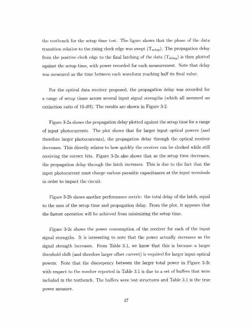
3-1 Transient simulation waveforms demonstrating bit decisions. ..... 44
3-2 Propagation delay through the latch plotted against setup time. The
input photocurrent was varied, and the input data is switched from 0
to 1. Clock frequency is 5-GHz. ................... .. 48
3-3 Sampling apertuture characterization for 0-1 step input. . ....... 50

3-4 In Situ eye diagram from simulation. ...................
3-5 Transient plot of the positive output terminal of the receiver during a
DC input photocurrent. Superimposed on the plot is the distribution
of threshold values from monte carlo simulation.
Layout photo of the EOS2 chip . . . . .
Organization of the EOS2 electrical cell.
An optical link in EOS2 . .........
Block diagram showing cell operation. .
Block diagram of scan chain cells.....
High-speed SEnable synchronization.
High-speed signal synchronization .
PRBS/pattern generator block . . . . .
Output transition counter with reference.
4-10 Snapshot implemented for the modulator
. . . . . . . . . 58
. . . . . . . . . . . . 58
.. . . . . . . 59
. . . . . . . . . . . 60
. . . . . . . . . . 62
. . . . . . . . . . 63
. . . . . . . . . . . 64
.. . . . . . . 65
. . . . . . . . . . . . . 66
and data receiver of EOS2. 67
Transient analysis testbench . . . . . . . ....
Offset compensation testbench. .........
Testbench for setup and hold time simulation.
Sampling aperture characterization testbench.
Variation analysis testbench. ...........
.. . . . . . . 73
.. . . . 74
. . . . . . . . . . . . . 74
. . . . . . . . . . . . . 75
. . . . . . . . 75
B-I Testbench for power measurement simulation . . . . . .
C-I Sampling apertuture characterization for 1-0 step input.
. . . . . . . 77
. . . . . . . 80
D-I Register design. ................. . . . . . . . . . . ....
D-2 M UX design . .. .. . . . . . . . . . . . . . . . . . . . . . . . . . . .
E-i Block diagram of scan chain cells. ................... .
F-I The output of the PRBS generator, driven at 5-GHz ..........
4-1
4-2
4-3
4-4
4-5
4-6
4-7
4-8
4-9
A-1
A-2
A-3
A-4
A-5
i
. . . . . 54

List of Tables
1.1 Summary of optical receivers scaled to 32nm. Power scaling for digital
designs follows P = fCVDD, with C scaling linearly with process.
Power scaling for analog designs follows a linear scaling with current
and supply, based on maintaining a constant transistor transconductance. 20
2.1 Example configuration data. Threshold values are found using Fig-
ure 2-7 ...... ............................ 37
3.1 Power consumption for each block of the data receiver during 5-GHz
operation with a 100-uA 'on' photocurrent. . ............... 45
F.1 Progression of PRBS pattern. . .................. . 90


Chapter 1
Introduction
This thesis presents an energy-efficient monolithically-integrated optical receiver
for photonic interconnects in a 32-nm CMOS process. The work will analyze the
various aspects of the receiver, focusing on challenges such as process variation, sen-
sitivity, energy-efficiency, and integrated photodiode modelling.
1.1 Background
Optics has been used to transmit high-bandwidth data since the 1970s, when it
was first used in long-haul interconnects. In computing, optical networks have been
envisioned as a replacement for electrical backbones since the early 1990s [2] when
they were used to connect multiple computers to form a single super-computer. Since
that time, Moore's law continued to drive CMOS gate sizes smaller and smaller,
increasing clock speeds. The price, however, was paid in power dissipation. Processor
manufacturers such as Intel and AMD drove clock speeds to the point where the heat
produced could not be pulled away fast enough, and so a practical limit in CPU clock
speed was reached in the range of 3- to 4-GHz. Designers had to find a way to keep
computation scaling, and the answer was found in parallelism.
Since the release of the first multi-core processors, the trend in industry and
academia has been to continue to increase the number of cores on each chip. At the
time of this proposal, it is common for consumer computers to have dual- or quad-

core processors, such as the Intel Core i7 [3]. More specialized consumer hardware
has seen 9-core processors, such as the IBM Cell in the Playstation 3 [4], and 16-core
server processors, such as the third-generation SPARC processor [5]. Going forward,
we can envision systems with upwards of 256 cores.
In order to fully harness the computing capability of many-core systems, commu-
nication between cores and with a shared off-chip memory must be extremely fast. In
past single-core processors, the number of long global wires constituted only a small
fraction of the total. However, with the emergence of multi-core systems, where each
core must be able to communicate with each other as well as off-chip memory, global
interconnects have become a major bottleneck. Power density requirements further
dictate that the communication must also be low power and energy-efficient. The
problem with electrical I/O is that even its projected performance will not satisfy
the bandwidth and energy-efficiency demands of many-core systems [1]. This is due
in part to the fact that electrical I/O performance is ceasing to scale with technol-
ogy, and is instead becoming channel-limited [6]. Integrated photonic links provide a
new type of channel for inter- and intra-chip I/O. Wavelength-division multiplexing
(WDM) allows for several high-speed data streams to be placed onto a single low-
latency waveguide, reducing the number of interconnects and increasing the energy
efficiency and bandwidth density.
1.2 Motivation
The reward of a monolithically-integrated optical link is high, but there are many
challenges that stand in its way. The characteristics of such a link are well-suited to
high-speed communication, but have significanly different characteristics than tradi-
tional electrical interconnect. As a result, it may be difficult for designers to adapt
to optical I/O design. Designers must be knowledgeable in optical device physics in
order to determine which of the limited materials and layers to use in a given semicon-
ductor process. They must be able to take these materials and create optical device
geometries that either route optical data or serve as an interface between the optical
i-1

and electrical domains. Finally, they must have a strong system-design background in
order to optimize the electrical-optical-electrial link as a whole. This thesis addresses
this emerging design issue through the implementation of an optical data receiver.
Each of the parts of the receiver will be described and analyzed, exemplifying how
designers must use their knowledge of both optics and electronics in order to exploit
optical I/O. This serves to help future designers by focusing on the most important
design parameters.
1.3 Previous Work
External Chip A Ring Modulator Driver Chip B Receiver
Lser Vertical Coupler Photo- , O\Soure and Tap V V Waveguide detector.
Ring Modulator Ring Modulator Mode Ring Filter Ring Filterwith A Resonance with 2 Resomnance Fiber with Xl Resonance with 2 Resonance
Figure 1-1: An integrated photonic link implementing WDM [1].
This section reviews the building blocks and previous work done on integrated
optical interconnects. A diagram of an integrated optoelectronic system is shown in
Figure 1-1, with the main building blocks being:
1. integrated photonic waveguide - the path along which the modulated optical
data can travel
2. optical modulator - converts electronic data into an optical signal
3. optical receiver - converts optically modulated data back into the electrical
domain
In Figure 1-1, the optical source is an off-chip continuous-wave laser. This laser
light is coupled onto the IC by means of a vertical coupler which redirects the light to
travel in the plane of the chip. Once propagating along the integrated photonic waveg-
uides, the continuous-wave laser light can be manipulated. Different wavelengths can
LM

be re-routed by means of wavelength-selective filters, and data can be imprinted onto
each wavelength by means of an optical modulator. The modulated light can be
placed onto a bus common with data modulated on different wavelengths, without
interference. This optically modulated data can then be routed to an optical receiver,
either on the same chip or a different one.
While these components have been demonstrated in the past, one of the key
challenges in this work is that the components must be monolithically integrated
onto a single wafer of silicon, in order to enable high energy efficiency and bandwidth
density. In the following sections, we outline each of the above components in more
depth.
1.3.1 Optical Waveguides
Optical confinement in any medium is created by an index difference between the
core and surrounding materials. Integrated photonic waveguides have been demon-
strated recently in two main ways: in special processes, such as silicon-on-insulator
(SOI); and in bulk CMOS processes [7]. In an SOI process, the waveguide core can
be created using the body, with the buried-oxide layer creating the cladding. In
bulk CMOS, the waveguide core can be made from the poly-silicon layer used to
create the unsilicided resistors, located above the shallow-trench isolation (STI). One
of the main problems with bulk CMOS integration is that the oxide layer is much
thinner, increasing optical loss to the substrate. In order to mitigate this effect, an
air-undercladding is created during post-processing, as demonstrated in [8].
1.3.2 Optical Modulators
The purpose of the optical modulator is to take an electrical signal, and imprint
it onto a continuous wave of light, generating an optically modulated signal. In this
work, resonant ring modulators are used. Resonant ring filters (Figure 1-2) are cir-
cular optical structures adjacent to a waveguide. Each filter is tuned to a particular
photon wavelength. At that wavelength, light travelling down the waveguide will cou-

ple into the filter and remain confined there, eventually being dissipated or dropped.
All other wavelengths will travel down the waveguide undisturbed, except for some
relatively small wavelength-dependent loss.
Figure 1-2: A ring with a modulator on the EOS2 test chip.
A modulator based on this structure exploits the fact that the resonant frequency
can be tuned thermally, or by injecting charge into the ring to change the index of
refraction. To generate an optical '0', the ring is tuned to the wavelength of interest
and the transmission through the waveguide is decreased. To generate an optical '1',
the ring is tuned away from the wavelength of interest, decreasing that wavelength's
confinement and increasing its transmission [9].
1.3.3 Optical Receivers
The final component in the optical link is the receiver, which converts the optically-
modulated data back into the electrical domain. This is accomplished by sensing the
photocurrent produced by a photodiode that is being illuminated, and converting the
current into a voltage waveform. Previous implementations can be broken down into
two main types of implementations: current-sensing and current-integrating. The
two methods are discussed further in the following subsections.
To date, the majority of optical receiver designs in the literature have addressed
telecommunications applications, where a single, discrete receiver is connected to a
fiber-optic cable and used to generate an electrical data signal. One major challenge
associated with this is the very large parasitic capacitance due to packaging of discrete
components. However, a major benefit is that since the phodiode is external, any
semiconductor material desired can be used. In contrast, in order to achieve a large
receiver density with high energy efficiency, we focus on monolithic integration. As a
- M

result, in this work we are constrained to the material selection available in the 32-nm
bulk CMOS process.
The performance of several recent optical receivers is summarized in Table 1.1.
The table shows the process, data rate, power consumption, and topology used. Also
shown are power and energy/bit numbers scaled to a 32-nm process node. This was
done in order to create a more accurate performance comparison with the receiver
proposed in this work.
Process Speed Power Power (mW) pJ/bit Topology(Gb/s) (mW) (scaled) (scaled)
[6] 90-nm 16 23 8.17 0.51 DDR Latch[10] 0.13-um SOI 4x10 120 19.7 0.492 TIA/Limit[11] 80-nm 20-GHz 2.2 0.88 - TIA[12] 0.13-um,Ge-on-SOI 10 30 4.92 0.492 TIA/Limit
This Work 32-nm, SiGe PD 5 0.5 0.5 <0.1 Latch
Table 1.1: Summary of optical receivers scaled to 32nm. Power scaling for digitaldesigns follows P = fCVD, with C scaling linearly with process. Power scaling foranalog designs follows a linear scaling with current and supply, based on maintaininga constant transistor transconductance.
The integration of all necessary optical and electrical components onto a single
substrate was recently demonstrated in [10], where a single SOI substrate was used to
create a 4xl0-Gb/s transceiver, with the photodiodes flip-chip bonded to the CMOS
die. The receiver consists of a TIA followed by a limiting amplifier. The input
impedance of the TIA is kept small by using resistive feedback. This allowed for
high-speed operation, despite the relatively large parasitic capacitance.
Current-Sensing Receivers
In current-sensing implementations, the input photocurrent is converted to a volt-
age waveform by means of some transimpedance gain. This can be accomplished by a
transimpedance amplifier, or as is the case in this work, a current-sense-amplifier. As
will be shown in Chapter 2, one advantage of this approach is that it easily enables
the implementation of a highly-digital design, with no biasing required at the input

(a) [11] (b) [12]
TIA F ..nt.En
Vdd
, LGndP"U
(c) Narasimha Data Recever [10] (d) Receiver-less Optical Clock Injection [13]
Figure 1-3: Optical data receivers from the literature.
nodes. The disadvantage however is that only the input photocurrent at the time of
evaluation is used, increasing the vulnerability due to random noise.Figure 1-3a shows the CMOS trans-impedance amplifer for the optical Clock Injecdata re-
ceiver presented in [11]. This work targeted low-power, high-bandwidth optical linksT Day
T. ----------------
VWeora~~
--------------,-------------------
ceiver presented in [11]. This work targeted low-power, high-bandwidth optical links

for short-distance fiber-optic interconnects. Standard TIA topologies were investi-
gated, and limitations in the 80-nm CMOS process used were discussed. The TIA
shown in Figure 1-3a consists of a modified conventional regulated cascode, and over-
comes process limitations such as low supply headroom in order to achieve its target
specification. The design also uses peaking inductors in order to increase the band-
width, which further illustrates the problem with analog-style optical receiver designs
going forward into more advanced CMOS processes. The photodiode capacitance for
the work was 220-fF.
In [12], the advantages of monolithic integration of the photodiode and receiver
circuit are discussed, with the benefits of the use of Germanium presented. The work
uses a Ge-on-SOI detector, which is stated to have a responsivity of 0.35 A/W and
an intrinsic capacitance of 30-fF. The TIA ( 1-3b) used is a differential, common-gate
topology, that also uses peaking inductors. The TIA is followed by a 5-stage limiting
amplifier, and then a buffer to drive a 50-Q load. The complete receiver operates at
12-Gb/s, and the authors note the low photodiode biases used.
Data-rate scaling through the implementation of wavelength-division multiplexing
(WDM) is presented in [10]. The strategy of the transceiver presented was to take
multiple 10-Gb/s links and put them in parallel in order to achieve higher data rates.
This was done to address the fact that the channel can become the most expensive
part of a long I/O link. The data receiver used is shown in Figure 1-3c. Similar to
the receiver presented in [12], it consists of a TIA front-end followed by a 5-stage
limiting amplifier and 50-Q output buffer. The photodiode is flip-chip bonded to the
die, with light directed to it by means of a holographic lens. What is remarkable
about this work is the level of optelectronic integration, with the optical transmitters
and receivers implemented on the same CMOS SOI chip.
Current-Integrating Receivers
Designs that use an analog amplifying front-end burn a lot of quiescent power in
order to achieve high bandwidth and low noise [14]. In current-integrating approaches,
the input photocurrent is integrated into a capacitance, which converts the signal

into a voltage waveform that is integrated over time. The capacitance can be some
fixed capacitance, the capacitance of the diode, or the parasitic capacitance of the
interfacing transistors. It can also be the capacitance of a programmable current
source [6] that continuously discharges the average photo-current. The advantage
of the current-integrating approach is that the input current signal is now being
integrated over as much as an entire bit time, increasing the sensitivity of the receiver.
The receiver will also be more robust to a random noise source at the input, as each
noise contribution should, on average, cancel over the integrating time.
The clearest example of an integrating-type receiver is presented in [13], and is
shown in Figure 1-3d. In this receiver-less design, two optical clock pulses that are
out of phase are propagated to two photodiodes that are stacked on top of each other.
As the optical clock pulses reach their target photodiodes, the photocurrent that is
generated is used to charge/discharge the node looking into the digital logic block.
The capacitance at this node is composed of the diode's own capacitances, as well
as any parasitic capacitances. Assuming that the diodes are well matched, and that
there is enough optical power and high-enough conversion efficiency, the input node
to the digital logic will have enough range to drive the following logic blocks.
Figure 1-3e shows the optical data receiver presented in [14]. One of the main
challenges with using clock-based designs that latch the decisions of comparators
is that there must be some reset phase in the operation. Since we only want to
use one photodiode and one waveguide to save area, this means that it is difficult
to achieve better than one bit per clock period. An innovative solution to this is
presented in [14], where double-data-rate (DDR) operation was achieved. The author
integrates the photocurrent from the diode onto its own parasitic capacitance. A
feedback loop substracts an average optical current from the capacitor in order to
prevent the capacitor's voltage from increasing to the supply. The bit decision is
then made by comparing the voltage on the capacitor to the voltage on the capacitor
from the previous bit. If the voltage is greater, then photocurrent has been generated
during this bit decision and an optical '1' is received. If the voltage is smaller (due
to the charge subtracted by the feedback loop), then an optical '0' is received. The

receiver implemented in [14] was able to resolve a 11-pA input current at 1.6-Gb/s
with a power consumption of only 3-mW. The design was implemented in a 0.25-tum
CMOS process with a photodiode capacitance of 420-fF.
Figure 1-3f shows an updated version of [14], as presented in [6], as part of a
complete optical transceiver. In [6], the receiver demultiplexes the data stream into
five parallel receivers by means of five different clock phases. Each of the data receivers
sequentially uses two consecutive clock phases to implement the double-sampling
previously described. This allows the receiver to integrate the input photocurrent for
an entire bit-time and then evaluate the decision for another bit-time, significantly
increasing the sensitivity. This yields a high data rate while only using a single
photodiode and a relatively low-speed clock.
1.4 Contributions of this Thesis
This thesis presents the first-generation implementation of an optical data receiver
for monolithically-integrated silicon photonic interconnects. The optical receiver pre-
sented is a photocurrent-sensing receiver that amplifies the input signal by means of a
modified sense amplifier. The amplification is enabled through the positive feedback
of two cross-coupled inverter structures in the latch.
The challenge in this work is to design a highly energy- and area-efficient receiver
for massively integrated applications, that is is robust to process and noise in a highly
digital environment. The additional practical challenge associated with this work is
that monolithic silicon photonic devices are still under development, so this receiver
has to be flexible enough to accomodate a large range of device variations. The issue
is compounded by the fact that the work is done in a pilot 32-nm process, where
creating a large and complex chip is extremely difficult.

1.5 Summary
In this chapter, the use of optical interconnects for emerging multi- and many-core
processors was presented. The main building blocks of an electrical-optical-electrical
link were outlined, with particular attention paid to the optical data receivers. The
two main types of optical data receivers (current-sensing and current-integrating) were
contrasted against each other. Finally, the design and implemenation of a highly-
digital, monolithically-integrated optical data receiver in a 32-nm process was then
introduced as the goal of this thesis.


Chapter
Receiver Design
The optical receiver presented in this work is a highly-digital, synchronous, current-
sensing data receiver that interfaces with a monolithically-integrated photodiode. The
simulated receiver will be shown to be able to resolve input photocurrents of less than
50-pA at 5-Gb/s with a power consumption of less than 500-pW (100fJ/bit). In this
chapter the optical receiver is introduced. An overview of the receiver illustrates its
basic operation. Each of the parts of the receiver is then presented and examined in
more detail.
2.1 Recever Block Diagram
+ + Buffer + VoutLatching Sense Dynamic-to-StaticSAmplifier V n Converter
V Buffer + - Vout-
Photodiode Vbuf- -Oglobal Clock
Clamp Vbuf+ enable Enable
Figure 2-1: Block diagram of the optical data receiver implemented in the EOS2 testchip.
The optical data receiver presented in this thesis is shown in Figure 2-1. The re-
ceiver consists of several highly-digital blocks, including one that provides feedback.
The front-end of the receiver consists of a monolithically-integrated photodiode con-
nected directly to a modified latching current-sense amplifier. The output of the latch
(dynamic signals Vdy,+, -) is then buffered and converted to static signals V,,t+, -
that are valid over an entire bit time. The buffered signals Vbuf+, - are also used
to drive a feedback block that shorts the photodiode once the bit decision has been
made.
The entire receiver is driven by a clock that can be disabled if the receiver is
not to be used. Disabling the clock eliminates switching-power consumption in the
rest of the receiver. The only block that would consume static current is the offset-
compensation block inside the Latching Sense Amplifer. A separate configuration bit
disables the bias in this block, eliminating power consumption in the disabled mode.
The optical receiver operates in two clock phases, receiving 1 bit per clock period.
In the reset phase (first half clock cycle), the sense amplifier is reset to a metastable
initial state. In the evaluation phase (second half clock cycle), the latching sense
amplifier evaluates the current generated by the photodiode. By the end of the
evaulation phase, the output of the sense amplifier has been resolved to a digital
value that is then stored at the onset of the next reset phase.
2.2 Photodiode
The main element that allows the optically-modulated data signal to be converted
into the electrical domain is the photodiode, which converts incident optical power
into electrical current that can be detected. The design, simulation, and implemen-
tation of the photodiode used in this work was done by Jason Orcutt. Some key
modelling parameters and theory of operation are presented in this section.
i ~i~-~i --i-^lii) i- iii lii--i:: --- i--i----~~~-'~-~-i'~~~~W*-i*~~il-.i~~

2.2.1 Semiconductor Material
The mechanism by which a photocurrent is generated by an optical optical signal
is the absorption of a photon, and consequently the generation of an electron-hole pair
in the depletion region of the diode. The electric field that exists in the depletion
region then causes the electron and hole to be swept to the n- and p-doped termi-
nals, respectively, creating a current that can be measured at the diode's terminals.
Some of the fundamental parameters to consider are the bandgap of the material,
which describes the amount of optical energy required to excite an electron from the
valence to conduction band and create an electron-hole pair, the wavelength of the
incident optical power, which describes how much energy each incident photon has
(Equation 2.1), and whether or not the the semiconductor material has a direct or
indirect bandgap. The absorption coeffecient, a [cm - 1] describes how much light is
absorbed by a material, and can be plotted as a function of wavelength.
heEphoto = (2.1)
Ge
E EEg,d,
0.6 0.8 1.0 1.2 1.4 1.6 1.8Wavelength [pm]
Figure 2-2: The absorption coeffecient plotted against wavelenth of light [15].
Figure 2-2 shows the absorption coefficients for silicon and germanium at various

wavelengths. Note that since silicon has an indirect bandgap structure, its absorption
rolls off slowly. Germanium, which has an indirect bandgap around 1.8-um also rolls
off, but at its direct bandgap between 1.5 and 1.6-nm the absorption increases quickly
with photon energy.
The photodiode material used in this work is a Silicon-Germamium (SiGe) al-
loy. The availability of this material is a fortunate coincidence. SiGe is becoming
more common in advanced CMOS processes, as the Germanium is implanted into the
drain regions of the PMOS transistors in order to improve mobility. We exploit the
availability of the Germanium in order to create the photodiodes.
With the photodiode created using SiGe, and the optical waveguides (which should
have as little absorption as possibile) created using polysilicon, an appropriate range
of wavelengths for the light in this work can then be selected. The wavelength should
be large enough that the light is not absorbed by the poly-silicon waveguide, but
also small enough that it can be absorbed by the high-absorption direct-bandgap of
the Germanium in the SiGe. The exact wavelength used will also be a function of
the mole fraction of Germanium, with the anticipated range for this process being
1200-1300-nm.
2.2.2 Geometry
Once the semiconductor materials for the photodiode have been selected, the ge-
ometry must be designed. The layout of the photodiode relative to the direction of the
incident optical power depends on the application, and will affect design metrics such
as the efficiency and responsivity of the diode, which describe how much current will
be generated per incident optical power. The efficiency of the photodiode describes
how many electron-hole pairs are generated per incident photon. The responsivity is
defined as the amount of photocurrent generated per incident optical power, and can
be used directly in a link-budget calcuation.
In the case of the EOS2 test chip, the incident optical power is propagating down a
poly-silicon waveguide, and must be absorbed near the termination of the waveguide.
Figure 2-3 is a simulation result that shows the intensity of the optical power through

Figure 2-3: A cross-sectional view of the waveguide showing the mode propagation.[Figure courtesy of Jason Orcutt]
the core of an integrated waveguide. It is the portion of the mode outside of the core
that will be absorbed.
Figure 2-4 shows a model of the photodiode placement relative to the waveguide
termination. The model (not to scale) shows that the photodiodes are made using
the same p-n junctions as in the MOSFETS of the process. The p-n junctions are
oriented radially away from the waveguide, ensuring that there is an absorptive region
along the entire length of the waveguide. Photodiodes are placed on each side of the
waveguide in order to maximize absorption. The terminals are then tied together
using the metal layers, in order to collect the photocurrent in parallel. A final layout
picture of the photodiode can be seen in the far-right of Figure 4-3b.
--- , I _I

Figure 2-4: A 3D model of one of the photodiodes implemented in EOS2.
2.2.3 Photodiode Model
One of main challenges with designing any system composed of both optical and
electrical elements is properly modelling one set of elements in a manner that fits
into the design environment of the other. We needed to create a model of the pho-
todiode that could be integrated into the existing electrical design flow. The basic
functionality of the photodiode is represented by a current source, representing the
photocurrent that is generated when the photodiode is excited by an optical source,
and a capacitance that is seen across the diode's terminals (Figure 2-5).
*l on,off diode
Figure 2-5: Photodiode Model
In this work, the modelling is particularly challenging, as all of the optical elements
are implemented monolithically in a CMOS process with relatively little information
'I- -,~ r - - -- I I I ~-
about critical doping concentrations and other photonic design and variation param-
eters.
As a result, we use reasonable estimates for the diode's parameters. The dark
current of the diode should be very small and is therefore negligible. This is because
the p-n junctions used are the same as those used in transistors, and the dark cur-
rent will be on the same order as any leakage. The relatively small dimension of
the diode enables fast operation even without a reverse bias, enabling the interesting
current-sensing receiver described in this work. The difference between the diode's
on- and off-currents was taken to be 10-dB, due to the expected extinction ratio of
the modulator implemented on the chip. The diode capacitance used is 10-fF. Note
that this capacitance is significanly smaller than other diode capacitances in the op-
tical communication literature, due to the fact that it is monolithically integrated.
While this is certainly good, the penalty that is paid is that in a monolithic imple-
mentation, the photodiode material selection is limited only to what is available in
the process. The absorption, and correspondingly the photocurrent and sensitivity,
therefore potentially suffer from monolithic integration.
2.3 Latching Sense Amplifier
For this thesis work, an optical data receiver based on a current-sense-amplifier
is proposed. The current-sense-amplifier with the photodiode connected to the in-
put terminals is show in Figure 2-6. As described in Section 2.2, the photodiode is
modelled as an ideal current source in parallel with a capacitance. The latch design
leverages the fact that the photodiode used can be operated without a reverse-bias
applied across its terminals. This allows for a fully differential, highly digital receiver
to be designed, without having to worry about biasing the diode.
In the reset phase, all of the latch's terminals are precharged to the supply. The
photodiode is shorted. During the evaluation phase, transistors M 1,2 are enabled
by the clock, and each branch of the latch begins to discharge. If an optical 1 is
received, then a photocurrent will be generated, causing current to flow from the node

Figure 2-6: The latching data receiver implemented on the EOS2 test chip.
in- to node in+. This will cause the negative branch of the latch to discharge more
quickly, and therefore latch low. In the absence of a photocurrent, the branches would
discharge at an equal rate, and (without offset compensation) the latch would not be
able to make a decision. Offset compensation will be examined in the next section,
and can help the negative branch to latch high in the absence of a photocurrent.
The latch's transistor sizes were selected based on speed and sensitivity constaints,
as detailed in [16]. NMOS transitors M1,2 are ideally made small, in order to maximize
the evalutation time of the latch. Non-minimum-size devices were used in order to
achieve the target data rate. The latch itself consists of two cross-coupled inverters
(NMOS M3 ,4 and PMOS M5,6). In each of the inverters, the NMOS-to-PMOS sizing
ratio was made larger than that used for a balanced inverter. This serves to lower
the threshold of the cross-coupled inverters, and again increases the evaluation time
where the positive-feedback integrates the input signal. Resetting the latch is achieved
through transistors M7 ,8,9,10 which precharge all of the internal nodes high. Transistor
--- ---lr~'-"~~"~""~"-*ri;i~:r-^-)?ic~~~ ~

M11 further balances the two latch branches in the reset phase. Transistors M 7,8,9,10,11
are ideally small to reduce parasitics.
2.4 Offset Compensation
Figure 2-7: 7-bit offset compensation scheme for latching data receiver.
The latching sense-amplifier presented in Section 2.3 is a differential structure
and is nominally perfectly balanced. This balance can be disrupted through process
variation, which can only be compensated after fabrication, and so a programmable
offset compensation block must be implemented. The offset compensation must have
a range that is sufficiently large to counter the effects of both optical and electrical
variation, but also enough resolution to measure the eye diagram in situ as will be
presented in Section 3.5.
The offset compensation is also required to upset the balance of the latch during
nominal operation. When an optical-1 is received, the photodiode in Figure 2-6
generates a current from node Vi,- to Vi,+. This will cause Vi,+ to discharge more
slowly and therefore latch high. When an optical-0 is receiver, though, little or no

photocurrent will be generated, and the latch input will appear to be approximately
zero. Without compensation, the decision that the latch will make will be random
and dependant on noise at the inputs. Offset compensation is therefore used in order
to raise the threshold of the latch, so that V,,t+ will always latch low for an optical-0.
140
120
100
80
60
40
20
00 20 40 60 80 100 120 1
DAC Code
(a) Offset Compensation Codes
0 20 40
(b) Integral
60 80 100 120 140 0 20 40 60DAC Code DAC C
Nonlinearity Error (c) Differential Non
Figure 2-8: Offset compensation performance.
80 100 120 140ode
linearity Error
The offset compensation is shown in Figure 2-7. The compensation consists of a
digitally-programmable binary-weighted current mirror (transistors M30-M43) that
pulls additional current off of one of the two input nodes shown in Figure 2-6. Transis-
tors M30-36, which have the same gate bias, have binary-weighted widths to generate
the binary-weighted currents. Transistors M3 7- 4 3 control which branches are enabled,
and are sized the same as M30-M36 to ensure that branches carrying more current
have a correspondingly smaller impedance. The node that is compensated is con-
trolled by transistors M46 and M47. The gate bias for the binary-weighted current
branches is generated by transistors M25- 29 . In the event that offet compensation is
-Clock Speed:5GHz
- .. . . ............
,. .. i i.
* 1 LSB= 1.1uA
0 .. :- 664 6 : j- 1-
-1"2 *
I I ---- --------- ----- .. .......... - - - - - --i : -lil - -
S1 LSB=uA
......... .... : i .................... .. ..................
.. : . :.... .... ... ... .... .... ... .... ... .... ... .... .. .., ...,, ir *
L ~ ! ! ! . . . . . . . . . ... . . . .. . . .= . . _ ... . .. . . . i +
-

not required, the current mirror can be completely shut off by turning M 24 on and
M25 off. This sets the bias voltage equal to zero and prevents any current from being
generated in the branches.
Figure 2-8 summarizes the performance of the offset compensation block. Figure 2-
8a shows the meta-stable input current that correspondes to of the 128 codes. The
range of compensation was determined based on variation analysis that will be further
analyzed in Section 3.2. It is interesting to note the non-ideality of the codes near the
origin. this shift in the transfer function is due to the capacitance that is added just
by turning on transistor M46. The magnitude of the shift then represents the amount
of current required to overcome this additional capicitance. Figures 2-8b and 2-8c
show the integral-nonlinearity error (INL) and differential-nonlinearity error (DNL)
of the DAC, respectively. These metrics describe the linearity of the DAC.
In order to configure the offset compensation, the following steps should be carried
out experimentally. Here they are done in simulation for the purpose of this thesis.
The results are summarized in Table 2.1.
1. Determine the threshold for the receiver when the input bit is an optical 0.
2. Determine the threshold for the receiver when the input bit is an optical 1.
3. Set the offset compensation to the code half-way between the two thresholds
found in steps 1 and 2.
ION,IoFF Optical '0' Optical '1' Optical DAC(p1 A) Threshold Threshold Threshold Configuration
120,12 9 103 56 100 0111100,10 8 80 44 101 001180,8 7 61 34 101 110160,6 6 44 25 110 011040,4 5 29 17 110 111020,2 2 14 8 111 0111
Table 2.1: Example configuration data. Threshold values are found using Figure 2-7

2.5 Latch Output Buffer
Vdyn +/- >0, Vbuf-/+
Figure 2-9: The output buffer of the optical receiver.
The latch shown in Figure 2-6 is followed by a buffer stage. The buffers are
implemented as inverters, as shown in Figure 2-9. The purpose of the buffers is to
increase the sensitivity of the latch at the cost of delay.
For a given clock speed, the sensitivity is improved as the capacitance seen at
the output nodes is a much weaker function of the previous bit received. This is
because the capacitance looking into the dynamic-to-static converter, presented in
section 2.6, depends strongly on the previous bit, which it holds on floating nodes
until the decision for the current bit is made.
During the implementation of the EOS2 test chip, an error was made in the
placement of this buffer. The output of the latch was fed directly into the input of
the dynamic-to-static converter. The buffered signal was used only in feedback for the
photodiode clamp. Not only does this error mean that the capacitances seen at the
decision nodes of the latch will depend on the previous bit, but the feedback clamp
is also delayed by an inverter delay. The simulation results presented throughout the
thesis use the flawed schematic just described, in order to be able to more closely
match measured results with simulation. The advantage of the flawed design is that
there is less delay between the clock signal and the output data becoming valid.
2.6 Dynamic to Static Converter
The dynamic-to-static converter used in the optical receiver is shown in Figure 2-
10. Dynamic-to-static conversion is necessary because the output decisions from the
latching sense-amplifier are only valid for half of a bit-time (they are reset during the

Vbuf- M21 M18 M19 M2 V buf
Vu- M20 M16 M1 M22 - Vbu+
Vout- M Vout +
M12 M13
Figure 2-10: Dynamic-to-static schematic.
other half). The output of the dynamic-to-static converter is valid over the entire bit
time.
The dynamic-to-static converter consists of two cross-coupled tristate buffers (tran-
sistors M12-19). While the clock is high, the latch output bits can be set through tran-
sistors M20-23 based on the decision of the sense-amplifier. During the receiver's reset
phase (I=0), the tristate buffers become cross-coupled inverters, holding their pre-
vious values. The output dynamic-to-static converter's output nodes are not driving
by any other signal, as V b; + /- are both high.
2.7 Photodiode Clamp
Vbuf+ In+
Vbuf- In-
Figure 2-11: The photodiode-clamping circuit used in the optical data receiver.
The photodiode clamping circuit used is shown in Figure 2-11. The clamp consists
of a single NAND-gate that drives an NMOS transistor. The NAND-gate is connected

to the outputs of the sense-amplifier, before the dynamic-to-static conversion. During
the precharge phase, the sense-amplifier outputs are both HIGH, and the NAND's
output will be 0. During the evaluation phase, the sense-amplifier's outputs start off
the same and then diverge to a decision. It is only once the divergence has occurred
that the NAND's inputs differ, yielding a HIGH signal at the output that enables the
clamping NMOS. Therefore, the photodiode is only shorted once the bit decision has
been made.
The photodiode must be shorted in order to prevent a forward-biasing of the sub-
strate. At the end of the evaluation phase, the photodiodes terminals are connected
to two virtual grounds (being held by transistors M1, 2 ). If additional photocurrent
causes Vi,- to go below ground, then the M2 will have to start pulling the node up
to ground, which an NMOS cannot do well. If Vi,- is driven low enough, the diode
formed by the N-doped drain of M2 and the P-type substrate could turn on.
2.8 Clock Enable
enable
Figure 2-12: The clock-enabling block for each optical data receiver.
The clock-enabling scheme is shown in Figure 2-12. The Figure shows that the
clock used for each data receiver is derived from a global high-speed clock. By setting
the enable bit low, the local clock will not oscillate, and the rest of the highly digital
receiver will not switch, eliminating power consumption aside from leakage.
2.9 Summary
This chapter introduced the highly-digital, synchronous, current-sensing data re-
ceiver presented in this work. The receiver's basic operation was outlined. Each

of the components of the receiver was then presented, with operation and design
decisions explained. In the next chapter, circuit simulations are presented in order
to further illustrate the circuit's functionality, and also to demonstrate the achieved
performance.

Chapter 3
Receiver Simulation
In the previous chapter we outlined the design of the optical data receiver, showing
how each of the blocks were designed and work together. In this chapter, the full
operation is shown with simulated results. The simulations further illustrate how the
receiver operates, as well as analyze the performance achieved.
3.1 Transient Simulation
The in-depth analysis of the optical data receiver starts by first looking at the
waveforms at the nodes of the data receiver. To do this, a transient simulation is set
up, as shown in the testbench Figure A-1. The current source of the photodiode's
model is set to be a pulsed current source, with each pulse representing a bit of data
to be received. The offset compensation is set such that the threshold value is placed
between the 1- and 0-bit threshold values, as determined by Table 2.1.
Figure 3-1 shows the receiver voltage waveforms during multiple bit decisions.
In this example, the photodiode on-current was set to 100-ipA, while the off-current
was only 10-pA, assuming an extinction ratio of 10-dB. The current signal (Figure 3-
ib) was initially low, and transitions HIGH in time for the first rising clock edge
(Figure 3-1a). When the clock transitions high, the two photodiode input nodes
(Figure 3-1c) both race toward ground. At 200-ps, the positive node has current
being driven onto it from the photodiode, while current is being removed from the

o 0.5
0 .
0.2 0.3 0.4 0.5 0.6 0.7 0.8 0.9 1Time (ns)
(a) Clock Signal
Time (ns)(b) Photodiode Current
> 0.5
0
z0.5
0
0.2 0.3 0.4 0.5 0.5 0.7 0.8 0.9Time (ns)
(c) Input Node Voltages
0.2 0.3 0.4 0.5 0.6Time (ns)
(d) VDYN
0.2 0,3 0.4 0.5 0,6Time (ns)
(e) V,,t+
Figure 3-1: Transient simulation waveforms
0.7 0.8 0.9 1
0.7 08 0.9
demonstrating bit decisions.
negative node at the same time. This causes the negative node to race toward ground
more quickly. Figure 3-1d shows the response of the dynamic decision nodes of the
receiver (labeled Vdy, + /- in Figure 2-6). During the reset phase, when the clock
44
~ i;L -- =----:~.-----r)l-;-~-i;_-~-_-1CI _

is LOW, all of the internal nodes are pre-charged HIGH. When clock goes HIGH
during the evaluation phase, it is clear that if an optical '1' is being received, the
cross-coupled inverters cause Vdan+ to latch high and Vday- to latch low. Similarly,
if an optical 'O' is being received, such as at 600- and 8 00 -ps, Vdyn+ will latch LOW
and Vday- will latch HIGH. The outputs of the basic receiver are dynamic however,
and must be integrated into a static system. Figure 3-le shows the positive output
of the dynamic-to-static converter. The data at this node is valid for an entire bit
period.
Power (uW)Latch 110.2
Offset Compensation 237.5Output Buffer 2.4
Dynamic-to-static Converter 12.6Photodiode Clamp 0.3
Clock Enable 53.4Total 416.4
Table 3.1: Power consumption for each block of the data receiver during 5-GHzoperation with a 100-uA 'on' photocurrent.
Power consumption analysis is presented in Table 3.1, where the power of each
block is shown for operation at 5-GHz and a photodiode 'on' current of 100-uA.
From the table, it is clear that the offset compensation block dominates the power
consumption. Despite the use of current mirrors with ratios larger than 1, this power
results from the total range required by the compensation, while ensuring that all
mirroring transistors are near saturation. It is important to note that this power
consumption will decrease should the offset not be required to shift so far. This may
be the result of a smaller photodiode 'on' current, or from process variation. In the
former case, the problem that would arise is that the measurable eye-diagram would
have less vertical resolution. That is, the number of offset codes required to sweep
out the vertical opening of the eye would decrease. Therefore, future work should
address an offset compensation scheme that can add resolution without requiring
such a large photodiode 'on' current (which requires a large compensation power). A

programmable array of gate capacitances is a good solution.
The energy-per-bit is computed from Table 3.1 to be 83.3-fJ/bit. From Table 1.1,
it is clear that the energy-per-bit of the data receiver is competitive with the current
state of the art, though it only represents simulated results. Power was measured
using the method presented in Appendix B.
3.2 Offset Compensation Simulation
The offset compensation block of the optical data receiver was introduced in the
previous chapter, and is a particularly crucial block. It is the means by which the
threshold of the receiver can be set in order to accomodate different incident optical
powers. It is also the means by which the eye diagram of the receiver will be measured.
As a result, the offset compensation transfer function must be determined carefully.
The testbench for the offset compensation simulation is shown in Figure A-2. The
figure shows that for each experiment, the input photocurrent is set to a DC value,
and an offset compensation code is set. A transient simulation is then run, with a
5-GHz clock driving the optical data receiver. For each compensation code, the DC
current value is increased over multiple simulations. When the positive output of the
receiver eventually latches positive, it means the meta-stable current-code pair has
been determined. The resulting transfer function was presented in Figure 2-8a.
3.3 Setup Time
One of the main metrics in evaluating the performance of a digital block is the
relationship between the setup time and the delay. The setup time is defined as the
time between a change in the input data and the rising edge of the clock. The delay
through the block is the time from the positive edge of the clock to the change in the
output of the block.
In this section we examine the effect of the data input's phase and magnitude
on the ability of the data receiver to evaluate the correct bit. Figure A-3 shows
.__. ~~;~~__;_~~_~ ~ ~. .~~. ~.._ _.....~.....l__,x --I- I- ------- ;l;x r.
the testbench for the setup time test. The figure shows that the phase of the data
transition relative to the rising clock edge was swept (Tsetup). The propagation delay
from the positive clock edge to the final latching of the data (Tdelay) is then plotted
against the setup time, with power recorded for each measurement. Note that delay
was measured as the time between each waveform reaching half its final value.
For the optical data receiver proposed, the propagation delay was recorded for
a range of setup times across several input signal strengths (which all assumed an
extinction ratio of 10-dB). The results are shown in Figure 3-2.
Figure 3-2a shows the propagation delay plotted against the setup time for a range
of input photocurrents. The plot shows that for larger input optical powers (and
therefore larger photocurrents), the propagation delay through the optical receiver
decreases. This directly relates to how quickly the receiver can be clocked while still
receiving the correct bits. Figure 3-2a also shows that as the setup time decreases,
the propagation delay through the latch increases. This is due to the fact that the
input photocurrent must charge various parasitic capacitances at the input terminals
in order to impact the circuit.
Figure 3-2b shows another performance metric: the total delay of the latch, equal
to the sum of the setup time and propagation delay. From the plot, it appears that
the fastest operation will be achieved from minimizing the setup time.
Figure 3-2c shows the power consumption of the receiver for each of the input
signal strengths. It is interesting to note that the power actually increases as the
signal strength increases. From Table 3.1, we know that this is because a larger
threshold shift (and therefore larger offset current) is required for larger input optical
powers. Note that the discrepency between the larger total power in Figure 3-2c
with respect to the number reported in Table 3.1 is due to a set of buffers that were
included in the testbench. The buffers were test structures and Table 3.1 is the true
power measure.

: --- 120-uA..... 100-uA
+ -- .... 80-uA+ .+ + * 60-uA
:o ++ ++ + + + + o 40-uA
S cooo + 20-uA
.000. .00 .0. 0,00o.
I I I i-10 0 10 20 30 40 5
Ttp (ps)(a) Propagation Delay plotted against the setup time.
(a) Propagation Delay plotted against the setup time.
Tetup (ps)
(b) Total Delay plotted against setup time.
-10 0 10 20 30 40Tsetup (pS)
(c) Average power over a bit period plotted against setup time.
Figure 3-2: Propagation delay through the latch plotted against setup time. Theinput photocurrent was varied, and the input data is switched from 0 to 1. Clockfrequency is 5-GHz.
i - - -- ----- 120-uA
....... 1 ................... .................. 0 0-u A
* 60-uA. ............. .......... ....................... .* 6 0-uA
0 40-uA... - + 20-uA
* * + + * * * * * 444* * * + 4* * * * 4* * * * * * *4 *
. . . . . . . . . . . . . . . . . . . . . . . . . . . . . . .. . .. . . . . . .
+ +:+++++ ++++++ t + ++ ++-+ ++++ + +:+++++ +++ ++I Ii i
_LI
1111ill
3.4 Characterization of the Receiver's Sampling
Aperture
This section characterizes the sampling aperture of the latch-based optical re-
ceiver. The sampling aperture gives us a way to measure the bandwidth of the re-
ceiver. The characterization follows the analysis presented in [17], where the latch's
bit decision is represented as a weighted time-average of the input signal. One dif-
ference between the work in this thesis and that in [17] is that our input signal is
current-mode. The DC gain that we present here is a then a transimpedance gain as
opposed to a unitless one.
The testbench for the aperture characterization is shown in Figure A-4. The input
signal consists of a photocurrent step that again assumes a 10-dB extinction ratio.
The step's phase relative to the clock is swept, and for each phase, the receiver's
threshold is swept by changing the offset compensation code. The latch's bit decision
is recorded. The phase-configuration-bit space can then be plotted, showing all of the
metastable points and yielding an eye diagram.
Figure 3-3 shows the the simulation results from the receiver's aperture analysis for
a 0-1 step transition (the results for a 1-0 step transition can be found in Appendix C).
Figure 3-3a shows the offset current required to bring the latch to a meta-stable
state for each phase of the input step. From the figure, we can see that if the step
signal arrives early (negative phase), then the input nodes have time to settle and the
input photocurrent appears as a DC signal. The meta-stable code is then predicted
by looking at Figure 2-8a. As the step occurs closer and closer to the clock edge,
its photocurrent will have less and less impact on the latch's decision. Less offset
current is required by the compensation block to match the input signal, and we see
a decrease in the metastable code. In the extreme, when the bit arrives much later
than the clock edge, the offset compensation block must only match the off-current
of the input signal. Again, this appears as a DC-input that can be predicted by
Figure 2-8a.
Implicit in the code plotted in Figure 3-3a is any non-linearity in the current-DAC

70
60
50
40
30
20
10
0-10 100 1 -50 0 50
phase (ps)
(b) IMS(7)
100 150
x 1010
phase (ps)
(c) SSF(T).
0 200 400 600Frequency GHz
(e) FFT(ISF)
Figure 3-3: Sampling
phase (ps)
(d) ISF(r-).
235
234
,_ 231
23040-uA 40-uA: BW=14.9-GHz
-- 60-uA 229 --- 60-uA: BW=14.9-GHz .............-- 80-uA ---- 80-uA: BW=14.9-GHz
228800 1000 0 5 10 15
Frequency GHz
(f) FFT(ISF) (zoom view)
apertuture characterization for 0-1 step input.
- 40-uA- - 60-uA-- - 80-uA
............... .---
... ......
-50 0 50phase (ps)
(a) cMS(-r)
0
2 0 K
0 -50 -100
~r -. -.r- -- ---, -.- .rr-x-- --- ----r--;; - ; -- i:r---iici-r;-;i-ii.;cr;;;.ii i;. i;r --a; ;i ;r~:il---r;r~r~li;r~;=r--l -~~~;ir~~B~" ;;~~ ':;~-~~~~i w~~;i_:: -;
L
i=.

shown in Figure 2-7. Using the transfer function in Figure 2-8a, the meta-stable code
(cMS) is mapped to a meta-stable input current (IMS), shown in Figure 3-3b.
The Step Sensitivity Function (SSF) is defined by Equation 3.2, and is used to
plot a normalized version of the IMS, shown in Figure 3-3c. If the slope of the step
transition is large, it means that the receiver is very sensitive to the arrival time of
the input step. The receiver's sampling aperture would be considered fast.
Is(T) - min(Ins(T))SSF-() (3.1)norm( maz(IMs(r)) - min(Ins(T))
ISForm(T) = SSForm(T) (3.2)
The Impulse Sensitivity Function (ISF) is defined in Equation 3.2 as the derivative
of the SSF, and is plotted in Figure 3-3d. Through examination of the SSF, we
determined that an SSF with a steeper slope has a smaller aperture in time during
which it samples its input. This is seen directly in Figure 3-3d, where a receiver with
a smaller aperture would appear to have a sharper impulse.
Since this impulse the same impulse that we are using to sample our imput, it must
be thin enough (have enough bandwidth) to accomodate our desired data rate. As
discussed in [17], the bandwidth of the latching receiver can be computed by taking
the FFT of the ISF and measuring the 3-dB bandwidth. Figures 3-3e and 3-3f show
the FFT of the ISF. From the figures, the bandwidth of the receiver is clearly larger
than 10-GHz for each of the input current step sizes measured. This verifies that the
latch is fast enough for the 5-Gb/s target data rate.
3.5 Eye Diagram
In the previous section we used the SSF and ISF to characterize the sampling
aperture of the latching optical receiver. We can also use the cfgMS to create an
in situ eye diagram. In order to obtain the eye diagram, the IMS is recorded for a
different bit transitions (010,100,101,000,etc) and then superimposed. The resulting

80 I
60
V 40 ...... 40 uA
20 ..
-100 -50 0 50 100 150 200 250 300 350time (ps)
(a) 40-uA step input.
60 ......
C_ 40 ......... -....... .. ........ .......... ....... .... t-.....6 O uA60
20 . .
....
-100 -50 0 50 100 150 200 250 300 350time (ps)
(b) 60-uA step input.
80 ....
-100 50 0 50 100 150 200 250 300 350time (ps)
(c) 80-uA step input.
Figure 3-4: In Situ eye diagram from simulation.
plot is shown in Figure 3-4, and represents a plot of metastable currents for each
phase. The plot is used to determine the optimal sampling phase and threshold value
for each optical signal power.
It is important to emphasize that this is an experiment that will be performed on-
chip, and will be the only method to measure an eye-diagram. The difference between
the chip measurment and the one presented here is that while the eye diagram shown
in Figure 3-4 is derived from a single ideal transient simulation for each phase and
offset value, the on-chip measurement will take the average of 220 such simulations

for each phase and threshold value.
3.6 Process Variation
One of the major challenges with using such an advanced CMOS process as 32-nm
is combating the process variation and mismatch. These effects were mitigated by
implementing an offset compensation block with sufficient range to accomodate the
worst variation. The offset compensation block was presented in Section 2.4. In this
section, the performance of the compensation block is examined through variation
analysis.
Process variation is first studied through examination of the threshold shifts of the
latch for a DC input current over several Monte Carlo simulations. The testbench for
the experiment is shown in Figure A-5. The figure shows taht for each simulation, the
input photocurrent is set to a DC value. A transient simulation is then run with the
offset compensation code slowly incremented through the transient simulation, such
that each code will be valid over several high-speed clock periods. When the code is
incremented to the point where the positive output of the data receiver transitions
from high to low, then the meta-stable code that corresponds to the DC input current
for that Monte Carlo run has been found. Note that this threshold measurement
differs from the one used in Section 3.2 because if a new transient simulation was run
for each offset code, the Monte Carlo parameters would be reset.
The results of the DC-input variation analysis are shown in Figure 3-5. The plots
show a transient simulation with a duration of 2560ns. The codes are swept from -127
through 127, as shown in Figure 3-5a, with each code being valid for 10-ns. With a
clock rate of 1-GHz used for this experiment, each code is valid for 10 clock periods,
eliminating the effects of switching the codes during the simulation.
Each input current bias was simulated with 30 Monte Carlo runs. The threshold
for each run was recorded, and the mean and standard deviations computed. The
Gaussian distributions are superimposed onto the threshold plots in Figures 3-5b- 3-
5f.

50
0-C. . ...... ..... . .. ...... . . .. .: .
0 0,5 15 2 25time (us)
(a) Offset Code
I 1____ . J .................L................ I.-rS. .. ..... ....... ....... .......... ...... .... ...... ... ... ....... .......U
0 0.5 1 1.5 2 2.5
time x 10(b) Idiode=0-pA
I I r ........... .. ....... I......... .. -
0 . . .............5 .-. . ....... .
.. .......... ..
-....... .................
.
0" .. ............... ., ":
V
I
0 . ............... .............. ....... .... ...... ........ ........ . . . . . .. . .!....-. .-13 -- -' ' -.......
I
1
0 5 ................. :................. "................. :..,/ .......... .. i...... . .. ..0 .5. .... ..... ., - - -
0 0.5 1 1.5 2 2.5
I
x 10etime
(f) Idiode=80-pA
I
Figure 3-5: Transient plot of the positive output terminal of the receiver during a DCinput photocurrent. Superimposed on the plot is the distribution of threshold valuesfrom monte carlo simulation.
l""l~u"~""m"l""x~""-~""""~
0 0.5 1 1.5 2 2.5time x lo
(c) Idiode=20- A
I r _ . _ ............ I .................. .
r...... "0 0.5 1 1.5 2 2.5
time x 10o
(d) Idiode=40-pA
MI ! r....... .................,
O 0.5 1 1.5 2 2.5time x lO.a
(e) Idiode=60-/tA
.... "-. .., ................ .
r
: i
Nominal DAC=0SI I--"m'°°' 0AC0 I
Nominal DAC=16
mean=13stdev=28
- - Nominal DAC=31
mean=28stdev=22
-- Nominal DAC=45
mean=39stdev=27
-- Nominal DAC=63
mean=64stdev=29
I
I
0 .5 .............. .. .................n - - - -.

From the plots, it is clear that the peak of the Guassian distribution is located near
the nominal threshold crossing with no variation, as expected. The figures also show
that Guassian curves spread themself over a wide range of offset codes. While this
partly implies that the variation is severe, it also shows that the offset compensation
has good resolution in this implementation, meaning that the offset code required will
be quite close to the true meta-stable threshold. The fact that the Gaussian curves
largely flatten out within the range of the compensation code indicates that the offset
compensation scheme also has sufficient tuning range. The triple-transition seen in
Figure 3-5b is due to the parasitic capacitance of the branch-selection switch itself.
It is clear that when the branch selection switch is moved from the positive-branch
to the negative branch, even when the offset code is zero, there is some ambiguity
created in the threshold of the comparator.
Finally, while the Gaussian curves from each of the plots overlap each other when
superimposed, implying that there exist variation combinations where receiving data
is impossible, it is important to remember that each data point represents a different
Monte Carlo simulation, and the metastable points for the on- and off-currents will
shift together for a given run.
3.7 Summary
This chapter built upon the understanding of the optical data receiver presented
in Chapter 2 by analyzing the performance of the receiver through a series of ex-
periments. The basic implementation and operation of the optical data receiver was
introduced, with assumptions made on the type of optical signal that will be received.
Then the main offset tuning mechanism was explored through its own calibration
testbench. The offset compensation block's ability to mitigate the effects of process
variation was presented, indicated that the receiver should work even in this advanced
CMOS process. The speed of the latch was explored by examining the different delays
associated with its operation. Finally, a sophisticated method for measuring an in
situ eye diagram yielded a predicted bandwith for the receiver.


Chapter 4
EOS2 Test Chip
Our research team has executed a test chip called EOS2 that implements the main
photonic building blocks listed in Section 1.3. The purpose of the chip is to serve as
a test vehicle through which each of the components can be fully characterized. The
chip contains many different combinations of modulators, receivers, and waveguides in
order to develop an experimental understanding of the characteristics of each design.
The large degree of redundency serves to combat the unknown severity of process
variation in the pilot 32-nm process run. The EOS2 chip was submitted for fabrication
in the Spring of 2008, and is due to return in the Fall of 2009. A layout photograph
is shown in Figure 4-1.
4.1 Chip Organization
The EOS2 chip is composed of optical components and the electrical circuits that
interface with them. The electrical circuits are grouped into cells, where each cell
contains two modulator drivers, two optical clock receivers, and two optical data
receivers. The cells also contain test structures such as Pseudo-Random Binary Se-
quence (PRBS) generators, counters, and data snapshots (Figure 4-2). Programming
of the configuration bits is achieved through a single scan chain which is routed
throughout the chip. Configuration bits are first shifted into the scan chain, and then
loaded into their respective circuits.

Figure 4-1: Layout photo of the EOS2 chip.
I II!~ I
I II I
tI IIi I
Bufferst !! I
1 !I
i !I! !
i High-speed clock buffer
L ---- ---- --- ---- -- ---- ---- --- ---- ---
Figure 4-2: Organization of the EOS2 electrical cell.
II - - - II - - Ir
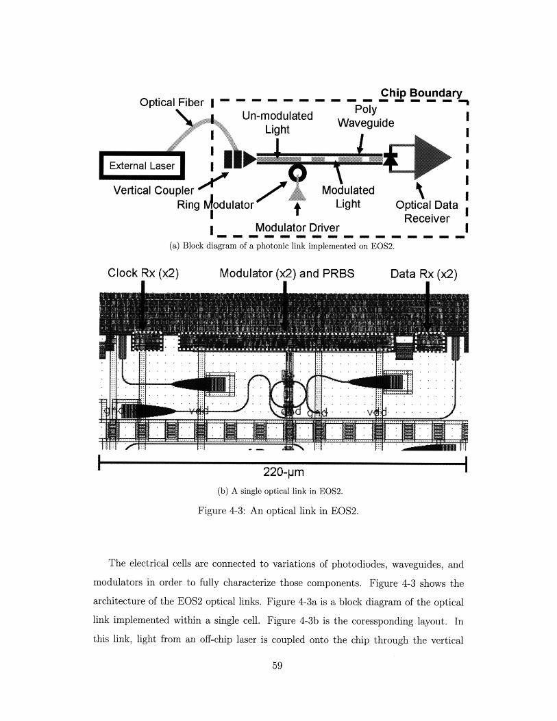
Chip BoundaryOptical Fiber I - - - - - -- -
Un-modulated PolyWaveguide
Light
External Laser I M
Vertical Coupler ModulatedRing Ivlodulator , Light Optical Data
I Receiver| Modulator Driver
(a) Block diagram of a photonic link implemented on EOS2.
Clock Rx (x2) Modulator (x2) and PRBS Data Rx (x2)
220-pm(b) A single optical link in EOS2.
Figure 4-3: An optical link in EOS2.
The electrical cells are connected to variations of photodiodes, waveguides, and
modulators in order to fully characterize those components. Figure 4-3 shows the
architecture of the EOS2 optical links. Figure 4-3a is a block diagram of the optical
link implemented within a single cell. Figure 4-3b is the coressponding layout. In
this link, light from an off-chip laser is coupled onto the chip through the vertical
NOW=

coupler (lower-left corner of Figure 4-3b. The light propagates along the waveguide,
and is modulated by the ring modulator in the center. This modulated data signal
then continues along the same waveguide until it is fed into the photodiode (top
right-hand corner of Figure 4-3b. The photodiode converts the optical signal into a
photocurrent, which is then detected by the data receiver.
The electrical test setup within each cell is shown in Figure 4-4. The data origi-
nates in the transmitter (TX) block, propagates through an optical waveguide, and
is received by a photodiode and the receivers of the receiver (RX) block.
On the transmitter's side, data from a PRBS/pattern generator drives both the
modulator, and a snapshot block. The PRBS/pattern generator can be configured to
generate either a pseudo-random bit sequence with a known starting point, or seed.
It can also be configured in a racetrack mode, with a pre-programmed 32-bit pattern
repeating itself. The snapshot is used to capture the most recent string of data that
was driven into the modulator.
Scanchain
Modulator SnapshoDriver RxData-2
PRBS aSeCounter
Snapshot RxClk-1
RxClk-2
Figure 4-4: Block diagram showing cell operation.
On the receiver's side of the block diagram, there are two types of input paths:
that for the optical data receiver and that for the optical clock receiver. In each
cell, there are two optical data receivers. One is connected to an optical circuit such
as that shown in Figure 4-3. The other is connect to either a vertically-illuminated
photodiode, or a waveguide connected directly to a vertical coupler. This second
- I I -I ar

photodiode is driven by optical data that has been modulated off-chip, and is a back-
up testing option in the event that the on-chip modulators do not work as expected.
The data receiver is selected by of a mux that drives a 32-bit snapshot block. The
snapshot records the 32 most recently received bits.
The receiver side also contains two clock receivers. The clock receivers are driven
by an off-chip optical clock, and are tested by counting the number of output electrical
pulses relative to a reference counter driven by an electrical clock. A mux is again
used to select which clock receiver is in operation.
The counter in the receiver block is a 20-bit pulse counter. The input to the
counter is driven by a third mux that selects between the data receiver's path and
the clock receiver's path. For the data receiver, the counter will be used primarily for
the measurement of an in situ eye diagram. It is important to be clear that in this
design, a bit-error-rate measurement cannot be performed on-chip.
4.2 Digital Test Structures
This section presents the implementations of the digital test structures used in
each cell of the EOS2 test chip.
4.2.1 Scan Chain
The EOS2 test chip is fully programmable by means of a single scan chain con-
sisting of a long array of registers. The scan chain consists of two different types of
cells: one for writing bits to the chip and one for reading bits from the chip. The
scan chain is controlled through five low-speed signals:
* Scan In (SI): the data bit to be loaded into the chip
* Scan Out (SO): the data bit to be read out of the chip
* Scan Clock (SCLK): the clock signal for reading and writing bits on the chip
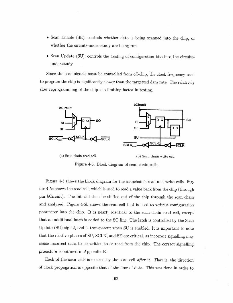
* Scan Enable (SE): controls whether data is being scanned into the chip, or
whether the circuits-under-study are being run
* Scan Update (SU): controls the loading of configuration bits into the circuits-
under-study
Since the scan signals must be controlled from off-chip, the clock frequency used
to program the chip is significantly slower than the targetted data rate. The relatively
slow reprogramming of the chip is a limiting factor in testing.
bCircuitbCircuit
0 0
SI D Q SO SI 1 D QSO
SE SE D Q
SCLK SUSCLKooK ._LK SO ! S1K U...SC xSCLK
SCLKnex L;K
(a) Scan chain read cell. (b) Scan chain write cell.
Figure 4-5: Block diagram of scan chain cells.
Figure 4-5 shows the block diagram for the scanchain's read and write cells. Fig-
ure 4-5a shows the read cell, which is used to read a value back from the chip (through
pin bCircuit). The bit will then be shifted out of the chip through the scan chain
and analyzed. Figure 4-5b shows the scan cell that is used to write a configuration
parameter into the chip. It is nearly identical to the scan chain read cell, except
that an additional latch is added to the SO line. The latch is controlled by the Scan
Update (SU) signal, and is transparent when SU is enabled. It is important to note
that the relative phases of SU, SCLK, and SE are critical, as incorrect signalling may
cause incorrect data to be written to or read from the chip. The correct signalling
procedure is outlined in Appendix E.
Each of the scan cells is clocked by the scan cell after it. That is, the direction
of clock propogation is opposite that of the flow of data. This was done in order to

avoid hold-time violations.
4.2.2 High-Speed Signal Synchronization
The EOS2 test chip has a single scan-enabling signal SEnable for both the low-
and high-speed blocks. When Senable is 1, all of the digital structures in the selected
portion of the chip shift data to the next structure. This means that the PRBS
is running in either of its two modes, the snapshot is receiving data, and the scan
chain is shifting data across in response to Sclk. It is important to recognize that
the while the transition edge of the Senable signal can be tightly controlled with
respect to the other low-speed signals (Sclk, Sreset, Supdate, Sin, Sout), its phase
relative the corresponding high-speed TX and RX clock edges is extremely difficult to
determine, and will vary across the chip. As a result, it is possible that the Senable
signal will transition near a high-speed positive clock edge in the local high-speed
blocks. This could potentially cause some registers to update, based on Senable=l1
and others based on Senable=0O, corrupting the data. The phase issue was addressed
SEnable D Q SEnable (local)
Figure 4-6: High-speed SEnable synchronization.
by re-synchronizing the Senable signal relative to the local high-speed clock phase.
Figure 4-6 shows the synchronization circuit. In the synchronization circuit, a single
register controls the local SEnable signal. On the positive high-speed clock edge, the
local SEnable signal is updated with the global value set by the Senable pin. The
local clock domain then has an entire bit time for Senable to settle, and the data will
processed correctly.

(a) A sweep of possible SEnable step phases.
(b) The synchronized local SEnable signal.
(c) Clock Signal.
Figure 4-7: High-speed signal synchronization.
4.2.3 PRBS/Pattern Generator
The PRBS/Pattern generator implemented in the EOS2 chip (Figure 4-8) consists
of 32 registers and supporting logic. The PRBS can be configured to achieve two
different modes of operation: PRBS mode and pattern mode. In the PRBS mode,
the registers create a 31-bit Linear Feedback Shift Register (LFSR). The outputs from
the 28th and 31st registers are summed and fed back into the first register in order
to achieve the correct sequence [18]. The 32nd register in the block is bypassed. In
the pattern mode, the feedback is changed and the 32nd register is not bypassed. A
32-bit pattern that has been loaded into the registers is allowed to shift arround in a
circle. In both PRBS and pattern modes, the initial pattern is set through the scan
chain. The same cells used to implement the scan chain's read cells were again used
in order to be able to have a pattern loaded into the PRBS. The SO bit of each stage
drives the SIN bit of the next, and all blocks share a common clock signal. A pattern

SE 0 A 1 W .
clock 1W II -- 1
Figure 4-8: PRBS/pattern generator block.
can be loaded into the PRBS through the circuitIn input of each scan cell. The figure
also shows how the outputs of the 31st and 28th stages are summed in a 1-bit adder
in order to create the necessary feedback bit. In PRBS mode, this bit is selected by
a MUX and sent to the input of the first scan cell. In pattern mode, the output of a
32nd register is instead routed back to the first scan cell.
Figure F-1 in Appendix F shows the first few outputs of the PRBS generator in
PRBS mode. Table F.1 will help the reader map out the states of the PRBS generator
and see how bit 0 and bit 3 are summed and fed back into bit 30.
4.2.4 Counters
The counter blocks in the EOS2 test chip are used to perform on-chip measure-
ments, with only the results being scanned out. This approach was necessary, as
there are not enough pads on the chip to measure every signal directly, and bringing
high-speed data off-chip is not a trivial task.
The counter functionality implemented in EOS2 is shown in Figure 4-9. The
two counters each consist of 20 registers, where the clock signal comes from the Q-
output of the previous stage, and each D-input comes from the stages own inverted
Q-output. The counters are both reset to a full count of all '1' and count down. The

Figure 4-9: Output transition counter with reference.
upper counter in the diagram is the reference counter and counts from 220 - 1 down
to zero. An additional register serves as a 21st bit, indicated whether or not a zero-
count has been reached. When the count reaches zero, the inputs to the reference
and measurement counters are switched to ground from the reference clock and input
signal, respectively. The data can then be scanned out of the chip and analyzed.
4.2.5 Snapshot
The snapshot is a 32-bit shift register that records the most recent receiver ouput
transititions. There is a snapshot for both the modulator driver and the data receiver.
The data from the snapshot can be scanned out of the chip, and th TX and RX
patterns compared. This can be used to determine the necessary phase difference
between the TX and RX high-speed clocks. Figure 4-10 shows the block diagram of
the snapshot implemented in EOS2. It is important to note that the snapshot uses
scan cells with some feedback as opposed to regular D-flip-flops. This is done in order
to preserve the data when SEnable is 0.
low

Figure 4-10: Snapshot implemented for the modulator and data receiver of EOS2.
4.3 Summary
This chapter presented the EOS2 test chip in which the optical data receiver was
implemented. The organization of the chip was outlined at both the chip and test-cell
levels. Each test cell was then described in detail, with an example optical link shown.
The high-speed test structures were then presented in order to show how some of the
simulation results shown in Chapter 3 will be measured.

I 11--l-I ---------- - =& -- -- - - --- ---- -- ",

Chapter 5
Conclusion and Future Work
5.1 Conclusion
The emergence of multi-core processors has created an I/O bottleneck both on-chip
between the cores, and between the cores and off-chip memory. Optical interconnects
are an attractive solution, as wavelength-division multiplexing allows multiple chan-
nels of information to be placed onto a single low-latency waveguide, reducing the
number of interconnects and increasing the speed of transmission.
This thesis presented a monolithically-integrated optical data link, focusing on
the design of an optical data receiver. The proposed receiver is a highly-digital,
current-sensing optical data receiver that interfaces with a monolithically-integrated
photodiode. The receiver is able resolve input photocurrents of less than 50-/pA at
a data rate of 5-Gb/s. The power consumption at this rate is less than 0.5-mW,
achieving better than 100-fJ/bit. This work demonstrated how an optical link de-
signer must first study the characteristics of the optical interface, and then design the
corresponding circuitry. The optical data receiver was presented as part of the EOS2
test chip, a flexible test vehicle that will demonstrate various optical components and
the electronic systems that interface with them.
5.2 Future Work
The field of monolithically-integrated photonic links for multi-core processors is
still an emerging one, and as such there are several areas in which more work can be
done, from the design of circuits, to the CAD-tools and infrastructure supporting the
actual design, to post-processing techniques.
5.2.1 Co-design of Optical Devices and Electrical Circuits
One of the main challenges described in this work related to the use of monolithically-
integrated photodiodes, which have a different set of characteristics than the discrete
photodiodes used in the literature. While a much more limited material selection
makes the design of highly-efficient and responsive monolithically-integrated photo-
diodes difficult, their smaller capacitances makes them ideal candidates for high-speed
receivers. Furthermore, by having the diode integrated with the rest of the circuitry,
the designer has complete control over the design of the circuits, the photodiode, and
also the interface between them. This gives the designer an unprecedented ability to
tightly integrate and co-design the two components. Going forward, we can expect
to see photodetectors that have been custom designed for a particular style of circuit
receiver. The design of the two components will be an iterative procedure, yielding a
more system-optimized architecture.
5.2.2 Optical Device Design, Layout, and Verification
One of the largest challenges, even in conventional circuit design, is ensuring
that performance does not degrade as the design matures from equations, to SPICE
simulations, to post-layout extracted simulations, to the final chip. Even verifying
that the layout and schemtic views contain identical connectivity is not a trivial task.
When optical links are incorporated into a current circuit CAD flow, the con-
nectivity problem only worsens. Designers must often manually check the interfaces
between the electrical and optical blocks. A full link simulation is also impossible,
as there is no optical simulator built into existing circuit CAD tools. Design rule
__-- .1 . ..... i. .. .. i.-.~;-.-j' I----- -- ------i--------ll----i.^"l~ ~ ";~~"~;

checking, which describes how the different layers in the chip's process are allowed
to be organizied, is also difficult, as many of the rules intended to protect transistor
and other electrical component fabrication must be broken in order to create the op-
tical structures. This requires a large degree of communication with the fabrication
company.


Appendix A
Testbench
IPD
Schematics
out+
out-
Figure A-i: Transient analysis testbench.
out+ tO I : tL

IPD
Cfg c fg -- fgin+ out+ out+
out+ r---- PD CP, RxDatat in- out- out-
0 q , clock
Figure A-2: Offset compensation testbench.
'PDt
, , cfg - cfgStin+ out+ out+IPD CPD RxData
out+ in- out- out-t
Sclocktsetupe :
tcqi
Figure A-3: Testbench for setup and hold time simulation.
I 1 1- -------

PD
cfg fg efg, t-in+ out+ out+,in
PD PD RxData
--- ,t in- out , out-
out+ ' - clock
It
tsetup I
Figure A-4: Sampling aperture characterization testbench.
IPD I
tfg Cfg
cfg - cfg in+ out+ out+
t IPD D RxData
out+ T in- out- out-
t clock
Figure A-5: Variation analysis testbench.


Appendix B
Power Measurement in Simulation
{Figure B-1: Testbench for power measurement simulation.
The testbench for measuring the average power is shown in Figure B-1. The
voltage source shown is the supply for the circuit under test. The current-controlled
current source is a current source with a gain of 1 that replicated the current from
the voltage source in the figure, with no feedback.
-I-
Vcap
Td I(t)dt
1- IAVGTC
77
(B.1)
(B.2)
(B.3)
The equation governing the voltage across the capacitor is given by Equation B.3.
The length of the transient simulation is given by T, the capacitance by C, and
the average current from the supply is given by IAVG. Rearranging the expression
and multiplying by the voltage from the supply, we can compute the average power
consumption over the simulation interval (Equation B.5).
Pavg = VDDIAVG (B.4)
=VDTD a (B.5)
By measuring the voltage across the capacitor at the end of the simulation, and
by knowing the capacitance and the length of the simulation. The average power can
then be computed.
i

Appendix C
Sampling Aperture Data
This appendix contains the sampling aperture data for a 1-0 step transition, as
opposed to the 0-1 step transition presented in Section 3.4. From the FFT, we verify
that the receiver has sufficient bandwidth for our data rate.

70
60
50
t 40
S30
20
10
0-10
0.8
0.6
C)
0.4
0.2
100 1200
50 -100 -50 0 50phase (ps)
(b) IMS(r)
x 1010
u bu uU 1ub -100 -50 0 50phase (ps) phase (ps)
(c) SSF(r). (d) ISF(r).
200 400 600 800 1000Frequency GHz
(e) FFT(ISF)
Figure C-1: Sampling apertuture
235
234
233
232
231
230
229
38R
0 5 10 15Frequency GHz
(f) FFT(ISF) (zoom view)
characterization for 1-0 step input.
-- 40-uA---- 60-uA
- - 80-uA
. .
-50 0 50phase (ps)
(a) cMS(r)
0 100 150
100 150
250
200
150
100
50
0
-50
-1000
.. . . . .. . . . .. . . ..... . . .. .
-40-uA: BW=17.3-GHz--- 60-uA: BW=14.9-GHz .
---- 80-uA: BW=17.3-GHzi i ,
.i .............. .. . . . .. . :. .. ..... .. .
- 40-uA....... ... . ....... - - - 60-uA -
--- 80-uA
"~;";"";': ---;-~~;;;;~ -- ~~~;;-~--~~;----~---~----~--~~~-- -----
. i I

Appendix D
Custom Standard Cell Library
There was no standard cell design library available in the advanced and experi-
mental 32-nm process that this thesis work was done in, and so a small standard cell
library had to be designed in order to implement the digital blocks. This appendix
outlines the design of some of the key components in the standard cell library and
the decisions that were made in their selection.
D.1 Register
Figure D-1 shows the register design used in the EOS2 test chip. It is a MASTER-
SLAVE style register from [19] [20], with the first latch being set when the clock is
low, and the second being set when the clock transistions from low to high. There
are several conservative design features implemented in the latch. Each half of the
latch is transparent for half of a clock period. During -= 0 clock phase, the first half
of the latch is transparent. Note that the feedback for the first half is disabled during
this time. This is to avoid competition. When the clock transisitions from low to
high, and )=1, the feedback in the first half of the latch is enabled, and the state is
stored. The second half of the latch is enabled for writing, with its feedback disabled.
The state of the second half of the latch is stored when the clock returns to zeros.
The Q-output of the register is isolated by means of an inverter. This is to prevent
whatever circuitry is driven by the latch from over-powering the latches feedback and

changing the state that is stored.
In the output loop, the clocked transistors were placed closer to the output node to
increase the speed of enabling the feedback. The register is asynchronously resetable.
D.2 MUX
The MUX used for standard cell library is a transmission-gate MUX, and is shown
in Figure D-2. The transission-gate style MUX was selected for its simplicity, but care
was required when preceding or following the gate by a long wire or large capacitance.
The reason for this is that the transmission-gate MUX is much weaker than a NAND-
based MUX. As area was not a primary concern in a 32-nm CMOS process, a NAND-
based MUX could have been a more appropriate choice.
(a) Register used in EOS2.
14 15 16 17 18 19Tsetup (ps)
(b) Clock-to-Q plotted against the setup time for the EOS2 register.
Figure D-1: Register design.
83
45
40
35
30
25
201-
.. .. ................. Tcq-T +T-- q setup
. . ". . . .............. ................................
3I I I I I I

inO
sell out
inl
Tsell
Figure D-2: MUX design.
__ii1
Appendix E
Scan Chain Control
E.1 Correct Signalling for the Scan Chain
This section explains the proper signalling sequence for the scanchain implemented
on the EOS2 test chip. Proper signalling ensures that the correct bits are read from
and written two the test circuits. The two different types of scan chain cells are shown
in Figure 4-5, and are repeated in Figure E-i for convenience.
bCircuitbCircuit
SO
SCLK--+-
(a) Scan chain read cell. (b) Scan chain write cell.
Figure E-1: Block diagram of scan chain cells.
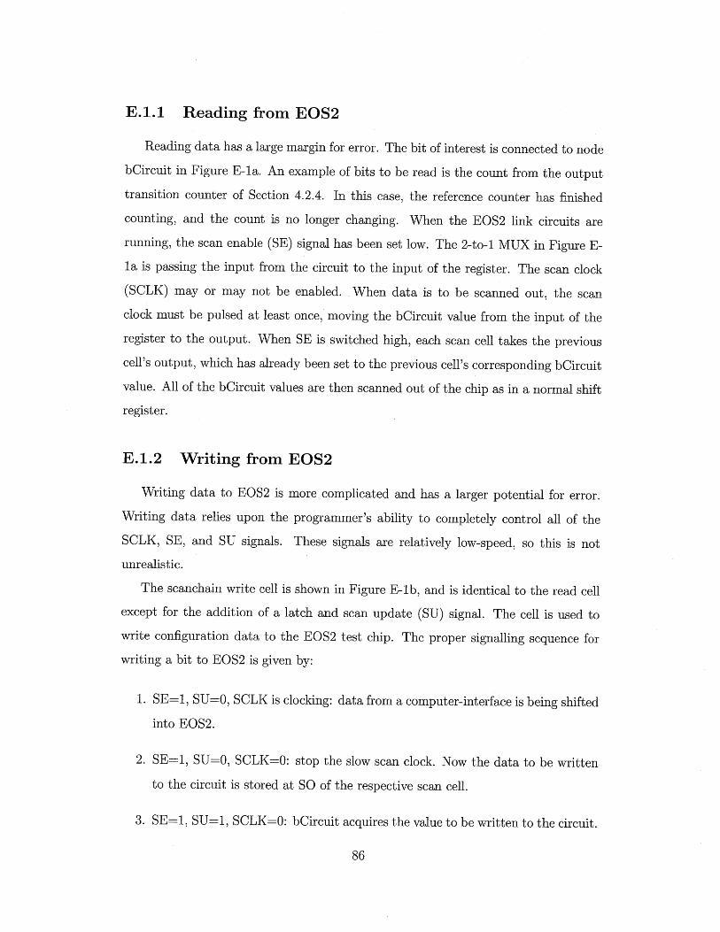
E.1.1 Reading from EOS2
Reading data has a large margin for error. The bit of interest is connected to node
bCircuit in Figure E-la. An example of bits to be read is the count from the output
transition counter of Section 4.2.4. In this case, the reference counter has finished
counting, and the count is no longer changing. When the EOS2 link circuits are
running, the scan enable (SE) signal has been set low. The 2-to-1 MUX in Figure E-
la is passing the input from the circuit to the input of the register. The scan clock
(SCLK) may or may not be enabled. When data is to be scanned out, the scan
clock must be pulsed at least once, moving the bCircuit value from the input of the
register to the output. When SE is switched high, each scan cell takes the previous
cell's output, which has already been set to the previous cell's corresponding bCircuit
value. All of the bCircuit values are then scanned out of the chip as in a normal shift
register.
E.1.2 Writing from EOS2
Writing data to EOS2 is more complicated and has a larger potential for error.
Writing data relies upon the programmer's ability to completely control all of the
SCLK, SE, and SU signals. These signals are relatively low-speed, so this is not
unrealistic.
The scanchain write cell is shown in Figure E-1b, and is identical to the read cell
except for the addition of a latch and scan update (SU) signal. The cell is used to
write configuration data to the EOS2 test chip. The proper signalling sequence for
writing a bit to EOS2 is given by:
1. SE=I, SU=O0, SCLK is clocking: data from a computer-interface is being shifted
into EOS2.
2. SE=1, SU=0O, SCLK=O: stop the slow scan clock. Now the data to be written
to the circuit is stored at SO of the respective scan cell.
3. SE=1, SU=I, SCLK=0O: bCircuit acquires the value to be written to the circuit.
~L-~X~I'~I"X^~.-(-~---.-_i.--I--_I----- i;~-il--.-r-i;~w~~wl~~;~l-i.~_-~~~~c~~

4. SE=-i, SU=0O, SCLK=0O: bCircuit holds the value to be written to the circuit
and is no isolated from the rest of the scan chain.
5. SE=0, SU=O, SCLK=O: the input to the register is now set to the value of the
bit that was intended to be written to EOS2 (the value of bCircuit).
6. SE=0, SU=0O, SCLK pulsed once: the value written to the circuit is now stored
at SO
7. SE=I, SU=0O, SCLK is clocking: data is scanned out from the chip to be ana-
lyzed. The scanchain read cells have read a value from the circuit. The scan-
chain write cells have stored the value that was written to the circuit. This can
be compared to the value that was intended to be written for verification.


Appendix F
PRBS Generation
This appendix shows the first 67 states of the PRBS pattern generator when seeded
with all l's. This is intended to give the reader an idea of how the prbs generates
all of the bit sequences with pulses of different lengths. Figure F-1 shows the output
of the PRBS generator being driven by a 5-GHz clock. In Table F.1, the reader can
follow through each of the states, seeing clearly how bits 0 and 3 are summed and fed
back into bit 30.
1
, _ ' 0 •. . . • .
0 5 10 15 20 25 30 35 40 45 50time (ns)
Figure F-1: The output of the PRBS generator, driven at 5-GHz.

bit 30 29 28 27 26 25 24 23 22 21 20 19 18 17 16 15 14 13 12 11 10 9 8 7 6 5 4 3 2 1 0 (output)
seed 1 1 1 1 1 1 1 1 1 1 1 1 1 1 1 1 1 1 1 1 1 1 1 1 1 1 1 1 1 1 1state 2 0 1 1 1 1 1 1 1 1 1 1 1 1 1 1 1 1 1 1 1 1 1 1 1 1 1 1 1 1 1 1state 3 0 0 1 1 1 1 1 1 1 1 1 1 1 1 1 1 1 1 1 1 1 1 1 1 1 1 1 1 1 1 1state 4 0 0 0 1 1 1 1 1 1 1 1 1 1 1 1 1 1 1 1 1 1 1 1 1 1 1 1 1 1 1 1state 5 0 0 0 0 1 1 1 1 1 1 1 1 1 1 1 1 1 1 1 1 1 1 1 1 1 1 1 1 1 1 1state 6 0 0 0 0 0 1 1 1 1 1 1 1 1 1 1 1 1 1 1 1 1 1 1 1 1 1 1 1 1 1 1state 7 0 0 0 0 0 0 1 1 1 1 1 1 1 1 1 1 1 1 1 1 1 1 1 1 1 1 1 1 1 1 1state 8 0 0 0 0 0 0 0 1 1 1 1 1 1 1 1 1 1 1 1 1 1 1 1 1 1 1 1 1 1 1 1state 9 0 0 0 0 0 0 0 0 1 1 1 1 1 1 1 1 1 1 1 1 1 1 1 1 1 1 1 1 1 1 1state 29 0 0 0 0 0 0 0 0 0 0 0 0 0 0 0 0 0 0 0 0 0 0 00 0 0 1 1 1 1 1state 30 0 0 0 0 0 0 0 0 0 0 0 0 0 0 0 0 0 0 0 0 0 0 0 0 0 0 0 0 1 1 1state 31 1 0 0 0 0 0 0 0 0 0 0 0 0 0 0 0 0 0 0 0 0 0 0 0 0 0 0 0 0 1 1state 32 1 1 0 0 0 0 0 0 0 0 0 0 0 0 0 0 0 0 0 0 0 0 0 0 0 0 0 0 0 0 1state 33 1 1 1 0 0 0 0 0 0 0 0 0 0 0 0 0 0 0 0 0 0 0 0 0 0 0 0 0 0 0 0 0state 34 0 1 1 1 0 0 0 0 0 0 0 0 0 0 0 0 0 0 0 0 0 0 0 0 0 0 0 0 0 0 0state 35 0 0 1 1 1 0 0 0 0 0 0 0 0 0 0 0 0 0 0 0 0 0 0 0 0 0 0 0 0 0 0state 36 0 0 0 1 1 1 0 0 0 0 0 0 0 0 0 0 0 0 0 0 0 0 0 0 0 0 0 0 0 0 0state 37 0 0 0 0 1 1 1 0 0 0 0 0 0 0 0 0 0 0 0 0 0 0 0 0 0 0 0 0 0 0 0state 38 0 0 0 0 0 1 1 1 0 0 0 0 0 0 0 0 0 0 0 0 0 0 0 0 0 0 0 0 0 0 0state 57 0 0 0 0 0 0 0 000 0 0 0 0 0 0 0 0 0 0 0 0 0 0 0 1 1 1 0 0 0 0state 58 0 0 0 0 0 0 0 0 0 0 0 0 0 0 0 0 0 0 0 0 0 0 0 0 0 1 1 1 0 0 0state 59 1 0 0 0 0 0 0 0 0 0 0 0 0 0 0 0 0 0 0 0 0 0 0 0 0 0 1 1 1 0 0state 60 1 1 0 0 0 0 0 0 0 0 0 0 0 0 0 0 0 0 0 0 0 0 0 0 0 0 0 1 1 1 0state 61 1 1 1 0 0 0 0 0 0 0 0 0 0 0 0 0 0 0 0 0 0 0 0 0 0 0 0 0 1 1 1state 62 1 1 1 1 0 0 0 0 0 0 0 0 0 0 0 0 0 0 0 0 0 0 0 0 0 0 0 0 0 1 1state 63 1 1 1 1 1 0 0 0 0 0 0 0 0 0 0 0 0 0 0 0 0 0 0 0 0 0 0 0 0 0 1state 64 1 1 1 1 1 1 0 0 0 0 0 0 0 0 0 0 0 0 0 0 0 0 0 0 0 0 0 0 0 0 0state 65 0 1 1 1 1 1 1 0 0 0 0 0 0 0 0 0 0 0 0 0 0 0 0 0 0 0 0 0 0 0 0
Table F.1: Progression of PRBS pattern.

Bibliography
[1] C. Batten, A. Joshi, J. Orcutt, A. Khilo, B. Moss, C. Holzwarth, M. Popovic,Hanqing Li, H. Smith, J. Hoyt, F. Kartner, R. Ram, V. Stojanovic, andK. Asanovic. Building manycore processor-to-dram networks with monolithicsilicon photonics. High Performance Interconnects, 2008. HOTI '08. 16th IEEESymposium on, pages 21-30, Aug. 2008.
[2] Rajeev J. Ram. MIT 6.731: Semiconductor Optoelectronics [course notes]. 2008.
[3] J.R. Sauer, D.J. Blumenthal, and A.V. Ramanan. Photonic interconnects forgigabit multicomputer communications. LTS, IEEE, 3(3):12-19, Aug 1992.
[4] Intel. Core i7 processor, 2008. http://www.intel.com/products/processor/corei7/index.htm.
[5] J. Kahle. The cell processor architecture, Nov. 2005.
[6] G. Konstadinidis, M. Rashid, P.F. Lai, Y. Otaguro, Y. Orginos, S. Param-palli, M. Steigerwald, S. Gundala, R. Pyapali, L. Rarick, I. Elkin, Yuefei Ge,and I. Parulkar. Implementation of a third-generation 16-core 32-thread chip-multithreading spares processor. Solid-State Circuits Conference, 2008. ISSCC2008. Digest of Technical Papers. IEEE International, pages 84-597, Feb. 2008.
[7] S. Palermo, A. Emami-Neyestanak, and M. Horowitz. A 90 nm cmos 16 gb/stransceiver for optical interconnects. Solid-State Circuits, IEEE Journal of,43(5):1235-1246, May 2008.
[8] J.S. Orcutt, A. Khilo, M.A. Popovic, C.W. Holzwarth, B. Moss, Hanqing Li,M.S. Dahlem, T.D. Bonifield, F.X. Kartner, E.P. Ippen, J.L. Hoyt, R.J. Ram,and V. Stojanovic. Demonstration of an electronic photonic integrated circuitin a commercial scaled bulk cmos process. Lasers and Electro-Optics, 2008 and2008 Conference on Quantum Electronics and Laser Science. CLEO/QELS 2008.Conference on, pages 1-2, May 2008.
[9] C.W. Holzwarth, J.S. Orcutt, Hanqing Li, M.A. Popovic, V. Stojanovic, J.L.Hoyt, R.J. Ram, and H.I. Smith. Localized substrate removal technique enablingstrong-confinement microphotonics in bulk si cmos processes. Lasers and Electro-Optics, 2008 and 2008 Conference on Quantum Electronics and Laser Science.CLEO/QELS 2008. Conference on, pages 1-2, May 2008.

[10] M. Lipson. Guiding, modulating, and emitting light on silicon-challenges andopportunities. Lightwave Technology, Journal of, 23(12):4222-4238, Dec. 2005.
[11] A. Narasimha, B. Analui, Y. Liang, T.J. Sleboda, S. Abdalla, E. Balmater,S. Gloeckner, D. Guckenberger, M. Harrison, R.G.M.P. Koumans, D. Kucharski,A. Mekis, S. Mirsaidi, Dan Song, and T. Pinguet. A fully integrated 4 10-gb/sdwdm optoelectronic transceiver implemented in a standard 0.13 um cmos soitechnology. Solid-State Circuits, IEEE Journal of, 42(12):2736-2744, Dec. 2007.
[12] C. Kromer, G. Sialm, T. Morf, M.L. Schmatz, F. Ellinger, D. Erni, and H. Jackel.A low-power 20-ghz 52-db-ohm transimpedance amplifier in 80-nm cmos. Solid-State Circuits, IEEE Journal of, 39(6):885-894, June 2004.
[13] C.L. Schow, L. Schares, S.J. Koester, G. Dehlinger, R. John, and F.E. Doany.A 15-gb/s 2.4-v optical receiver using a ge-on-soi photodiode and a cmos ic.Photonics Technology Letters, IEEE, 18(19):1981-1983, Oct.1, 2006.
[14] C. Debaes, A. Bhatnagar, D. Agarwal, R. Chen, G.A. Keeler, N.C. Helman,H. Thienpont, and D.A.B. Miller. Receiver-less optical clock injection for clockdistribution networks. Selected Topics in Quantum Electronics, IEEE Journalof, 9(2):400-409, March-April 2003.
[15] A. Emami-Neyestanak, D. Liu, G. Keeler, N. Helman, and M. Horowitz. A 1.6gb/s, 3 mw cmos receiver for optical communication. VLSI Circuits Digest ofTechnical Papers, 2002. Symposium on, pages 84-87, 2002.
[16] S. Mukhopadhyay, R.V. Joshi, Keunwoo Kim, and Ching-Te Chuang. Variabilityanalysis for sub-100nm pd/soi sense-amplifier. pages 488-491, March 2008.
[17] M. Jeeradit, J. Kim, B. Leibowitz, P. Nikaeen, V. Wang, B. Garlepp, andC. Werner. Characterizing sampling aperture of clocked comparators. In VLSICircuits, 2008 IEEE Symposium on, pages 68-69, June 2008.
[18] Peter Alfke. Efficient shift registers, Ifsr counters, and long pseudo-random se-quence generators. Technical report, Xilinx, 1996.
[19] V. Stojanovic, V. Oklobdzija, and R. Bajwa. Comparative analysis of latchesand flip-flops for high-performance systems. In Computer Design: VLSI in Com-puters and Processors, 1998. ICCD '98. Proceedings. International Conferenceon, pages 264-269, Oct 1998.
[20] G. Gerosa, S. Gary, C. Dietz, Dac Pham, K. Hoover, J. Alvarez, H. Sanchez,P. Ippolito, Tai Ngo, S. Litch, J. Eno, J. Golab, N. Vanderschaaf, and J. Kahle.A 2.2 w, 80 mhz superscalar rise microprocessor. Solid-State Circuits, IEEEJournal of, 29(12):1440-1454, Dec 1994.