MgO Magnetic Tunnel Junction sensors in Full Wheatstone Bridge ...
95
MgO Magnetic Tunnel Junction sensors in Full Wheatstone Bridge configuration for in-chip current field detection Raquel de Jesus Gandum Rato Gon¸ calves Flores Disserta¸ c˜ ao para a obten¸c˜ ao de Grau de Mestre em Engenharia F´ ısica Tecnol´ ogica J´ uri Presidente: Professor Jo˜ao Carlos Carvalho de S´a Seixas Orientador: Professora Susana Isabel Pinheiro Cardoso de Freitas Vogal: Professor Paulo Jorge Peixeiro de Freitas Outubro de 2010
-
Upload
dangnguyet -
Category
Documents
-
view
240 -
download
0
Transcript of MgO Magnetic Tunnel Junction sensors in Full Wheatstone Bridge ...
MgO Magnetic Tunnel Junction sensors in Full
Wheatstone Bridge configuration for in-chip current
field detection
Raquel de Jesus Gandum Rato Goncalves Flores
Dissertacao para a obtencao de Grau de Mestre em
Engenharia Fısica Tecnologica
Juri
Presidente: Professor Joao Carlos Carvalho de Sa Seixas
Orientador: Professora Susana Isabel Pinheiro Cardoso de Freitas
Vogal: Professor Paulo Jorge Peixeiro de Freitas
Outubro de 2010


Agradecimentos
Gostaria de agradecer em primeiro lugar a Professora Susana Cardoso, por me ter orientado e ajudado
durante este projecto, e ao Professor Paulo Freitas por me ter dado a oportunidade de trabalhar no INESC-
MN, com a sala limpa e todos os seus recursos ao meu dispor para este trabalho. Gostaria ainda de agradecer
ao Professor Candid Reig, do Departamento de Engenharia Electronica, da Universidade de Valencia, pela
sua inteira disponibilidade para me ajudar ao longo do projecto e ainda pela preciosa ajuda na realizacao e
discussao das medidas efectuadas em Valencia.
Um grande obrigado a todos os colegas e tecnicos do INESC-MN pela disponibilidade e ajudas prestadas
sempre que foi necessario, sem os quais nao teria sido possıvel chegar onde cheguei. Obrigado ainda a todos
aqueles que me proporcionaram um local de trabalho com muita alegria, boa disposicao e simpatia.
Agradecco aos meus colegas e amigos de mestrado pelo apoio e companheirismo e ainda a todos os meus
amigos que estiveram sempre presentes para dar animo e alegria a minha vida, em especial ao Ricardo por
ter estado la sempre que precisei.
Finalmente, ficarei para sempre agradecida e em dıvida para com a minha famılia pelo apoio incondicional
que me foi prestado em todos os aspectos que um curso acarreta para a vida. Um obrigada profundo as pessoas
mais importantes da minha vida: a minha mae Maria do Ceu, aos meus irmaos Manuel e Andre, a minha tia
Juquinha, a minha avo Catarina e a minha prima Monica. Agradeco ainda a famılia Raquel por todo o seu
apoio e carinho. E ainda ao Ze Maria pela sua companhia, que apesar de nao ser humano tambem faz parte
da famılia.
Obrigado ao meu avo Rato que me ensinou a ser uma pessoa melhor. Todos sentimos a sua falta!
iii

Resumo
Hoje em dia, e mais do que nunca, no que respeita a circuitos electronicos, a precisao e o controlo tornam-se
extremamente importantes, especialmente quando se trata de dispositivos relacionados com microeletronica,
onde medidas de corrente electrica, potencia e energia tem sido alvo de preocupacao. Por isso, dispositivos
precisos, facilmente integraveis, de baixo consumo energetico e baixo custo sao exigidos e sao essencialmente
necessarios em circuitos integrados, sistemas micro-eletromecanicos (MEMS), entre outros.
Juncoes de efeito de tunel magneticas (MTJ) tem sido utilizados como sensores de correntes electricas
em circuitos integrados. Alem disso, estes sensores tambem tem sido utilizados em configuracao de ponte de
Wheatstone para medicoes de baixas correntes.
Assim sendo, neste trabalho sao apresentados sensores MTJ em ponte de Wheatstone para deteccao de
corrente electrica em circuitos integrados com uma nova configuracao: cada elemento resistivo da ponte
consiste num conjunto de sensores MTJ ligados em serie, em vez de um unico elemento. O objetivo e medir
o campo criado por uma corrente electrica, aplicada em pistas incorporadas no chip durante o processo de
microfabricacao, reduzindo a separacao entre a fonte do campo e os elementos sensitivos, levando a uma
maior sensibilidade. Para obter uma ponte de Wheatstone completa e balancada, as pistas de corrente tem
que ser apropriadamente desenhadas.
Utilizando series de 18 MTJ elementos, alimentados por uma corrente de 100μA, obteve-se uma ponte
de Wheastotne com uma sensibilidade de 0.267 mVmAVb
= 1.334 mVOeVb
, e com um regiao linear de 40Oe, onde a
resistencia de entrada obtida para este dispositivo foi 544.96Ω. A tensao de “offset” obtida foi de −1.27mV .
Obteve-se uma R × A para a juncao de MgO de 1.82kΩ · μm2. Quando comparados com os dispositivos ja
existentes anteriormente, este novo tipo de pontes mantem o seu funcionamento ate tensoes de alimentacao
de 40V.
Palavras-chave: Sensores magnetoresistivos, Sensores MTJ de MgO, Pontes de Wheatstone, Sensores
de corrente
v

vi

Abstract
Nowadays and more than ever, control and precision regarding electronic circuits becomes very important,
especially concerning microelectronic devices where electrical current, power and energy measurements have
been a matter of concern. New precise, integrable, low power consumption and low cost devices are demanded
and they are mainly needed in integrated circuits (IC), systems-on-chip (SOC), micro-electromechanical
systems (MEMS), among others.
Magnetic tunnel junctions (MTJ) have been currently used as sensors for electrical currents measurements
in IC. In addition, these sensors have also been used in Wheatstone bridge configuration for low current
measurements.
So, Full Wheatstone bridges magnetic-tunnel-junction-based sensors for electrical current sensing at the
IC level are presented, with a new configuration: the resistive elements of the Wheatstone bridges consist
in arrays of MgO MTJ’s elements connected in series, instead of bridges with one single MTJ has resistive
element. The goal is to measure the field created by an electrical current, driven through paths incorporated
in the chip during the microfabrication process, reducing the separation to the sensing elements, leading to
improved sensitivity. And in order to get a full balanced Wheatstone bridge, the current paths need to be
properly designed.
Using series of 18 MTJs elements, biased with 100μA, it was obtained a bridge presenting a sensitivity of
0.267 mVmAVb
= 1.334 mVOeVb
, with linear behavior in the range of 40 Oe, where the bridge’s input resistance was
544.96Ω. The offset voltage of the transfer curve was −1.27mV and the R×A of the junction was determined
as 1.82kΩ · μm2. As a great improvement comparing to the previously existing devices, these new type of
bridges can hold up to voltages of 40V without breaking down.
Keywords: Tunneling magnetoresistance (TMR) sensors, MgO MTJ, Wheatstone bridge, Current
sensors
vii

viii

Contents
Acknowledgements . . . . . . . . . . . . . . . . . . . . . . . . . . . . . . . . . . . . . . . . . . . . . iii
Resumo . . . . . . . . . . . . . . . . . . . . . . . . . . . . . . . . . . . . . . . . . . . . . . . . . . . v
Abstract . . . . . . . . . . . . . . . . . . . . . . . . . . . . . . . . . . . . . . . . . . . . . . . . . . . vii
Contents ix
List of Figures xiii
List of Tables xv
1 Motivation 1
2 Theoretical Background 3
2.1 Magnetism and magnetic materials . . . . . . . . . . . . . . . . . . . . . . . . . . . . . . . . . 3
2.1.1 Diamagnetic materials . . . . . . . . . . . . . . . . . . . . . . . . . . . . . . . . . . . . 3
2.1.2 Paramagnetic materials . . . . . . . . . . . . . . . . . . . . . . . . . . . . . . . . . . . 4
2.1.3 Ferromagnetic materials . . . . . . . . . . . . . . . . . . . . . . . . . . . . . . . . . . . 4
2.1.4 Ferrimagnetic materials . . . . . . . . . . . . . . . . . . . . . . . . . . . . . . . . . . . 5
2.1.5 Antiferromagnetic materials . . . . . . . . . . . . . . . . . . . . . . . . . . . . . . . . . 5
2.2 Micromagnetism for ferromagnetic materials . . . . . . . . . . . . . . . . . . . . . . . . . . . . 6
2.2.1 Zeeman Energy . . . . . . . . . . . . . . . . . . . . . . . . . . . . . . . . . . . . . . . . 6
2.2.2 Exchange Energy . . . . . . . . . . . . . . . . . . . . . . . . . . . . . . . . . . . . . . . 6
2.2.3 Anisotropic Energy . . . . . . . . . . . . . . . . . . . . . . . . . . . . . . . . . . . . . . 7
2.2.4 Demagnetizing Energy . . . . . . . . . . . . . . . . . . . . . . . . . . . . . . . . . . . . 8
2.2.5 Neel Energy . . . . . . . . . . . . . . . . . . . . . . . . . . . . . . . . . . . . . . . . . . 9
2.2.6 Interlayer Coupling . . . . . . . . . . . . . . . . . . . . . . . . . . . . . . . . . . . . . . 9
2.2.7 Hysteresis Loop . . . . . . . . . . . . . . . . . . . . . . . . . . . . . . . . . . . . . . . . 10
2.3 Magnetoresistance . . . . . . . . . . . . . . . . . . . . . . . . . . . . . . . . . . . . . . . . . . 10
2.3.1 Anisotropic Magnetoresistance Effect - AMR . . . . . . . . . . . . . . . . . . . . . . . 11
2.3.2 Giant Magnetoresistance Effect - GMR . . . . . . . . . . . . . . . . . . . . . . . . . . 11
2.3.3 Tunneling Magnetoresistance Effect - TMR . . . . . . . . . . . . . . . . . . . . . . . . 13
2.3.4 Linear MTJs . . . . . . . . . . . . . . . . . . . . . . . . . . . . . . . . . . . . . . . . . 15
3 Experimental Facilities 19
3.1 Sputtering Deposition Systems . . . . . . . . . . . . . . . . . . . . . . . . . . . . . . . . . . . 19
3.1.1 Nordiko 2000 . . . . . . . . . . . . . . . . . . . . . . . . . . . . . . . . . . . . . . . . . 20
3.1.2 Nordiko 7000 . . . . . . . . . . . . . . . . . . . . . . . . . . . . . . . . . . . . . . . . . 21
3.1.3 UHV II . . . . . . . . . . . . . . . . . . . . . . . . . . . . . . . . . . . . . . . . . . . . 22
3.1.4 Alcatel SCM450 . . . . . . . . . . . . . . . . . . . . . . . . . . . . . . . . . . . . . . . 22
3.2 Ion Beam Deposition Systems . . . . . . . . . . . . . . . . . . . . . . . . . . . . . . . . . . . . 23
ix
3.3 Reactive Ion Etch . . . . . . . . . . . . . . . . . . . . . . . . . . . . . . . . . . . . . . . . . . . 24
3.3.1 LAM Research Rainbow Plasma Etcher . . . . . . . . . . . . . . . . . . . . . . . . . . 24
3.4 Pattern Transfer and Lithography: Direct Write Laser Optical Lithography (DWL) . . . . . . 25
3.4.1 Vapor Prime . . . . . . . . . . . . . . . . . . . . . . . . . . . . . . . . . . . . . . . . . 26
3.4.2 Photo-resist coating and developing . . . . . . . . . . . . . . . . . . . . . . . . . . . . 26
3.4.3 Optical Lithography Exposure . . . . . . . . . . . . . . . . . . . . . . . . . . . . . . . 27
3.4.4 Pattern transfer processes . . . . . . . . . . . . . . . . . . . . . . . . . . . . . . . . . . 28
3.5 Characterization . . . . . . . . . . . . . . . . . . . . . . . . . . . . . . . . . . . . . . . . . . . 29
3.5.1 Magnetic Thermal Annealing . . . . . . . . . . . . . . . . . . . . . . . . . . . . . . . . 29
3.5.2 Vibrating Sample Magnetometer (VSM) . . . . . . . . . . . . . . . . . . . . . . . . . . 30
3.5.3 Profilometer . . . . . . . . . . . . . . . . . . . . . . . . . . . . . . . . . . . . . . . . . . 30
3.5.4 Ellipsometer . . . . . . . . . . . . . . . . . . . . . . . . . . . . . . . . . . . . . . . . . 31
4 TMR based sensors: Wheatstone Bridge for Electrical Current Sensing 33
4.1 Wheatstone Bridge . . . . . . . . . . . . . . . . . . . . . . . . . . . . . . . . . . . . . . . . . . 33
4.1.1 Quarter Bridge Configuration . . . . . . . . . . . . . . . . . . . . . . . . . . . . . . . . 34
4.1.2 Half Bridge Configuration . . . . . . . . . . . . . . . . . . . . . . . . . . . . . . . . . . 34
4.1.3 Full Bridge Configuration . . . . . . . . . . . . . . . . . . . . . . . . . . . . . . . . . . 34
4.2 Application: Electrical current sensing . . . . . . . . . . . . . . . . . . . . . . . . . . . . . . . 35
4.3 Noise and detectivity of an array of tunnel junctions . . . . . . . . . . . . . . . . . . . . . . . 37
4.4 Device design . . . . . . . . . . . . . . . . . . . . . . . . . . . . . . . . . . . . . . . . . . . . . 38
4.5 Microfabrication . . . . . . . . . . . . . . . . . . . . . . . . . . . . . . . . . . . . . . . . . . . 39
4.5.1 Stack Deposition . . . . . . . . . . . . . . . . . . . . . . . . . . . . . . . . . . . . . . . 39
4.5.2 Bottom Electrode Definition . . . . . . . . . . . . . . . . . . . . . . . . . . . . . . . . 39
4.5.3 Junction Pillar Definition . . . . . . . . . . . . . . . . . . . . . . . . . . . . . . . . . . 40
4.5.4 Electrode Insulation . . . . . . . . . . . . . . . . . . . . . . . . . . . . . . . . . . . . . 40
4.5.5 Top Electrode Definition . . . . . . . . . . . . . . . . . . . . . . . . . . . . . . . . . . . 41
4.5.6 Sensors Insulation . . . . . . . . . . . . . . . . . . . . . . . . . . . . . . . . . . . . . . 41
4.5.7 Current Lines Definition . . . . . . . . . . . . . . . . . . . . . . . . . . . . . . . . . . . 42
4.5.8 Final Passivation . . . . . . . . . . . . . . . . . . . . . . . . . . . . . . . . . . . . . . . 42
4.5.9 Annealing . . . . . . . . . . . . . . . . . . . . . . . . . . . . . . . . . . . . . . . . . . . 42
4.5.10 Encapsulation . . . . . . . . . . . . . . . . . . . . . . . . . . . . . . . . . . . . . . . . . 42
4.6 Characterization . . . . . . . . . . . . . . . . . . . . . . . . . . . . . . . . . . . . . . . . . . . 43
4.6.1 MR Curves . . . . . . . . . . . . . . . . . . . . . . . . . . . . . . . . . . . . . . . . . . 43
4.6.2 I-V curves . . . . . . . . . . . . . . . . . . . . . . . . . . . . . . . . . . . . . . . . . . . 45
4.6.3 AC Characterization . . . . . . . . . . . . . . . . . . . . . . . . . . . . . . . . . . . . . 46
4.6.4 Thermal Characterization . . . . . . . . . . . . . . . . . . . . . . . . . . . . . . . . . . 47
5 Sensors Characterization and Results 49
5.1 Sensors design . . . . . . . . . . . . . . . . . . . . . . . . . . . . . . . . . . . . . . . . . . . . . 49
5.2 Results . . . . . . . . . . . . . . . . . . . . . . . . . . . . . . . . . . . . . . . . . . . . . . . . . 50
5.2.1 Calibration of the field created by the electrical current . . . . . . . . . . . . . . . . . 51
5.2.2 DC measurements . . . . . . . . . . . . . . . . . . . . . . . . . . . . . . . . . . . . . . 52
5.2.3 AC measurements . . . . . . . . . . . . . . . . . . . . . . . . . . . . . . . . . . . . . . 56
5.2.4 Thermal measurements . . . . . . . . . . . . . . . . . . . . . . . . . . . . . . . . . . . 57
6 Conclusions 61
Bibliography 63
x

A Masks 65
B Run Sheet 67
xi


List of Figures
2.1 Magnetic moment of atoms in diamagnetic materials . . . . . . . . . . . . . . . . . . . . . . . . . 4
2.2 Paramagnetism effect . . . . . . . . . . . . . . . . . . . . . . . . . . . . . . . . . . . . . . . . . . 4
2.3 Ferromagnetic behavior . . . . . . . . . . . . . . . . . . . . . . . . . . . . . . . . . . . . . . . . . 5
2.4 Ferrimagnetic ordering . . . . . . . . . . . . . . . . . . . . . . . . . . . . . . . . . . . . . . . . . . 5
2.5 Antiferromagnetic ordering . . . . . . . . . . . . . . . . . . . . . . . . . . . . . . . . . . . . . . . 5
2.6 Coercive field effect exemplification . . . . . . . . . . . . . . . . . . . . . . . . . . . . . . . . . . . 8
2.7 Demagnetizing field . . . . . . . . . . . . . . . . . . . . . . . . . . . . . . . . . . . . . . . . . . . 9
2.8 Neel coupling . . . . . . . . . . . . . . . . . . . . . . . . . . . . . . . . . . . . . . . . . . . . . . . 9
2.9 RKKY exchange coupling . . . . . . . . . . . . . . . . . . . . . . . . . . . . . . . . . . . . . . . . 10
2.10 Hysteresis loop of a ferrogmanetic material . . . . . . . . . . . . . . . . . . . . . . . . . . . . . . 11
2.11 Spin Valve structure . . . . . . . . . . . . . . . . . . . . . . . . . . . . . . . . . . . . . . . . . . . 12
2.12 Magnetic Tunnel Junction structure . . . . . . . . . . . . . . . . . . . . . . . . . . . . . . . . . . 13
2.13 Synthetic Antiferromagnetic structure . . . . . . . . . . . . . . . . . . . . . . . . . . . . . . . . . 13
2.14 Spin Dependant Tunneling effect . . . . . . . . . . . . . . . . . . . . . . . . . . . . . . . . . . . . 14
2.15 Spin depedent tunneling effect scheme . . . . . . . . . . . . . . . . . . . . . . . . . . . . . . . . . 15
2.16 Free and pinned layers with parallel anisotropies . . . . . . . . . . . . . . . . . . . . . . . . . . . 16
2.17 Parallel anisotropy solution: square transfer curve . . . . . . . . . . . . . . . . . . . . . . . . . . 17
2.18 Parallel anisotropy solution: linear transfer curve . . . . . . . . . . . . . . . . . . . . . . . . . . . 17
2.19 Free and pinned layers with perpendicular anisotropies . . . . . . . . . . . . . . . . . . . . . . . . 18
2.20 Crossed anisotropy solution: linear transfer curve . . . . . . . . . . . . . . . . . . . . . . . . . . . 18
3.1 Schematic view of a magnetron sputtering system . . . . . . . . . . . . . . . . . . . . . . . . . . . 19
3.2 N2000 schematic view . . . . . . . . . . . . . . . . . . . . . . . . . . . . . . . . . . . . . . . . . . 20
3.3 N7000: picture (left) and schematic view (right) . . . . . . . . . . . . . . . . . . . . . . . . . . . 21
3.4 UHVII: front view picture (left) and side view schematic (right) . . . . . . . . . . . . . . . . . . . 22
3.5 Alcatel SCM450 picture (left) and chamber schematic view (right) . . . . . . . . . . . . . . . . . 23
3.6 Schematic view of IBD systems . . . . . . . . . . . . . . . . . . . . . . . . . . . . . . . . . . . . . 24
3.7 LAM front view picture . . . . . . . . . . . . . . . . . . . . . . . . . . . . . . . . . . . . . . . . . 25
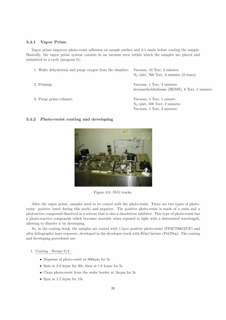
3.8 SVG tracks . . . . . . . . . . . . . . . . . . . . . . . . . . . . . . . . . . . . . . . . . . . . . . . . 26
3.9 Photo-resist mask designed by optical lithography . . . . . . . . . . . . . . . . . . . . . . . . . . 27
3.10 Picture of DWL system . . . . . . . . . . . . . . . . . . . . . . . . . . . . . . . . . . . . . . . . . 27
3.11 Illustration of the lift-off process . . . . . . . . . . . . . . . . . . . . . . . . . . . . . . . . . . . . 28
3.12 Illustration of the etch process . . . . . . . . . . . . . . . . . . . . . . . . . . . . . . . . . . . . . 28
3.13 Annealing setup . . . . . . . . . . . . . . . . . . . . . . . . . . . . . . . . . . . . . . . . . . . . . 29
3.14 Temperature cycle during magnetic thermal annealing . . . . . . . . . . . . . . . . . . . . . . . . 29
3.15 DMS model 880 VSM picture . . . . . . . . . . . . . . . . . . . . . . . . . . . . . . . . . . . . . . 30
3.16 Example of a VSM measurement for a bulk structure annealed at 240◦C . . . . . . . . . . . . . . 30
3.17 Profilometer’s picture . . . . . . . . . . . . . . . . . . . . . . . . . . . . . . . . . . . . . . . . . . 31
xiii

3.18 Ellipsometer’s picture . . . . . . . . . . . . . . . . . . . . . . . . . . . . . . . . . . . . . . . . . . 31
4.1 Wheatstone bridge circuit . . . . . . . . . . . . . . . . . . . . . . . . . . . . . . . . . . . . . . . . 33
4.2 Different Wheatstone bridge configurations . . . . . . . . . . . . . . . . . . . . . . . . . . . . . . 35
4.3 Magnetic field generated by an 160μm wide and 0.3μm thick current line . . . . . . . . . . . . . 36
4.4 Magnetic field generated by an 25μm wide and 0.3μm thick current line . . . . . . . . . . . . . . 36
4.5 Current lines configurations . . . . . . . . . . . . . . . . . . . . . . . . . . . . . . . . . . . . . . . 38
4.6 MTJ’s stack deposited in N2000 . . . . . . . . . . . . . . . . . . . . . . . . . . . . . . . . . . . . 39
4.7 Scheme of bottom electrodes definition . . . . . . . . . . . . . . . . . . . . . . . . . . . . . . . . . 39
4.8 Picture of bottom electrodes . . . . . . . . . . . . . . . . . . . . . . . . . . . . . . . . . . . . . . 39
4.9 Junction pillar definition . . . . . . . . . . . . . . . . . . . . . . . . . . . . . . . . . . . . . . . . . 40
4.10 Picture of junction pillars . . . . . . . . . . . . . . . . . . . . . . . . . . . . . . . . . . . . . . . . 40
4.11 Bottom electrodes and junction pillars insulation . . . . . . . . . . . . . . . . . . . . . . . . . . . 40
4.12 Top electrodes definition . . . . . . . . . . . . . . . . . . . . . . . . . . . . . . . . . . . . . . . . . 41
4.13 Picture of top electrodes. . . . . . . . . . . . . . . . . . . . . . . . . . . . . . . . . . . . . . . . . 41
4.14 Insulating layer between sensors and current lines . . . . . . . . . . . . . . . . . . . . . . . . . . . 41
4.15 Current paths definition: scheme (left) and picture (right) . . . . . . . . . . . . . . . . . . . . . . 42
4.16 Picture of a die mounted on a chip carrier and wirebonded . . . . . . . . . . . . . . . . . . . . . 43
4.17 Manual transport measurement setup picture . . . . . . . . . . . . . . . . . . . . . . . . . . . . . 43
4.18 Electric circuit for two probe measurements . . . . . . . . . . . . . . . . . . . . . . . . . . . . . . 44
4.19 I-V measurement setup picture . . . . . . . . . . . . . . . . . . . . . . . . . . . . . . . . . . . . . 45
4.20 I-V curves measurement: equivalent electric circuit (left) and picture with electrical scheme (right) 46
4.21 Experimental setup for AC characterization . . . . . . . . . . . . . . . . . . . . . . . . . . . . . . 46
4.22 Electric scheme of the AC measurements . . . . . . . . . . . . . . . . . . . . . . . . . . . . . . . . 47
4.23 Termal characterization setup picture . . . . . . . . . . . . . . . . . . . . . . . . . . . . . . . . . 47
5.1 Details of a series of MTJ’s elements and of only one element . . . . . . . . . . . . . . . . . . . . 49
5.2 Mask design of different current lines configurations . . . . . . . . . . . . . . . . . . . . . . . . . 50
5.3 Description of the several batches performed and the experimental issues associated . . . . . . . 51
5.4 V-I transfer curve for a series of 18 sensors . . . . . . . . . . . . . . . . . . . . . . . . . . . . . . 52
5.5 MR transfer curve for a series of 18 sensors . . . . . . . . . . . . . . . . . . . . . . . . . . . . . . 52
5.6 MR transfer curves for the 4 resistive elements of one bridge . . . . . . . . . . . . . . . . . . . . . 53
5.7 Electric circuit of a MR transfer of a resistive element . . . . . . . . . . . . . . . . . . . . . . . . 53
5.8 Resistance equivalent of a wheatstone bridge . . . . . . . . . . . . . . . . . . . . . . . . . . . . . 54
5.9 VI transfer curve of a ”S” type bridge . . . . . . . . . . . . . . . . . . . . . . . . . . . . . . . . . 55
5.10 VI transfer curve of a ”S” type bridge for 13.6V of biasing . . . . . . . . . . . . . . . . . . . . . . 55
5.11 Bridge output as function of biasing voltage . . . . . . . . . . . . . . . . . . . . . . . . . . . . . . 56
5.12 AC characterization for a “S” type bridge . . . . . . . . . . . . . . . . . . . . . . . . . . . . . . . 56
5.13 AC characterization for a “P” type bridge . . . . . . . . . . . . . . . . . . . . . . . . . . . . . . . 57
5.14 Sensitivity of “S” and “P” bridges as function of temperature . . . . . . . . . . . . . . . . . . . . 58
5.15 Voltage offset of “S” and “P” bridges as function of temperature . . . . . . . . . . . . . . . . . . 58
A.1 Mask with 160 μm wide current lines . . . . . . . . . . . . . . . . . . . . . . . . . . . . . . . . . . 65
A.2 Mask with 25 μm wide current lines . . . . . . . . . . . . . . . . . . . . . . . . . . . . . . . . . . 66
A.3 Label of colors of AutoCad masks . . . . . . . . . . . . . . . . . . . . . . . . . . . . . . . . . . . 66
xiv

List of Tables
3.1 Deposition setpoints for each material in N2000 system . . . . . . . . . . . . . . . . . . . . . . . 20
3.2 Standart conditions of operation of the N7000 modules . . . . . . . . . . . . . . . . . . . . . . . . 21
3.3 Deposition conditions for UHVII . . . . . . . . . . . . . . . . . . . . . . . . . . . . . . . . . . . . 22
3.4 SiO2 deposition setpoints in Alcatel SCM450 system . . . . . . . . . . . . . . . . . . . . . . . . . 23
3.5 IBD systems set values for the assist gun . . . . . . . . . . . . . . . . . . . . . . . . . . . . . . . 24
3.6 Setpoints for SiO2 etching in the LAM tool . . . . . . . . . . . . . . . . . . . . . . . . . . . . . . 25
5.1 Batches carried out in the experimental work . . . . . . . . . . . . . . . . . . . . . . . . . . . . . 50
5.2 Thermal coefficients . . . . . . . . . . . . . . . . . . . . . . . . . . . . . . . . . . . . . . . . . . . 59
xv

Chapter 1
Motivation
This master’s thesis is in the scope of the partnership between INESC-MN and the Department of Elec-
tronic Engineering, University of Valencia, which has the goal to develop Full Wheatstone Bridges for current
sensing applications, where the absence of a voltage offset is of extreme importance. The project started in
2003 using as electrical current sensors spin-valves, later in 2004 current straps were integrated in the device
and the Alumina magnetic tunnel junctions started to be used as field sensors, and in 2005 it was created
an improved design where the current straps were also integrated in the device but with spin-valves, instead
magnetic tunnel junctions.
Finally, the goal of this master’s thesis was to develop a new design, still with the current straps integrated,
but using MgO magnetic tunnel junctions, which present higher values of magnetoresistance than the spin-
valves or the alumina MTJ. The new design also included a new improvement: the magnetic tunnel junctions
were connected in series, in order to improve the detectivity and the electric robustness of the device.
1


Chapter 2
Theoretical Background
2.1 Magnetism and magnetic materials
Micromagnetism has to do with the interactions between magnetic moments on sub-micrometer length
scales. The best approach to such matter is to start with the Maxwell’s equations for both the electric and
magnetic fields in the presence of matter:
∇ ·D = ρ ∇×E = −∂B∂t
∇ ·B = 0 ∇×H = J+ ∂D∂t
Assuming that the there are no current, J, no electric field, E, and that the magnetics fields present are
quasi-static, the set of four equations reduces to only two:
∇ ·B = 0 ∇×H = 0
The magnetic induction vector, B is given by:
B = μ0(H+M) (2.1)
where μ0 is the vacuum magnetic permeability (μ0 = 4π × 10−7N/A2 ) and M is the magnetization of
the material. The total magnetic field, H, can be expressed as the sum of the external applied field Ha (the
field existent in the absence of medium) plus the demagnetizing field, Hd (factor due to the presence of the
material).
Magnetic materials can be classified into five major groups, according to their natural ordering and
response to an external magnetic field. Next can be found a brief description about each magnetic material
properties [1][2][3].
2.1.1 Diamagnetic materials
In a diamagnetic material, the atoms have no permanent magnet moment in the absence of an external
magnetic field, once their orbital shells are filled, having no unpaired electrons.
However, when exposed to a magnetic field, a magnetization is produced proportional to the applied field:
M = χH (2.2)
3
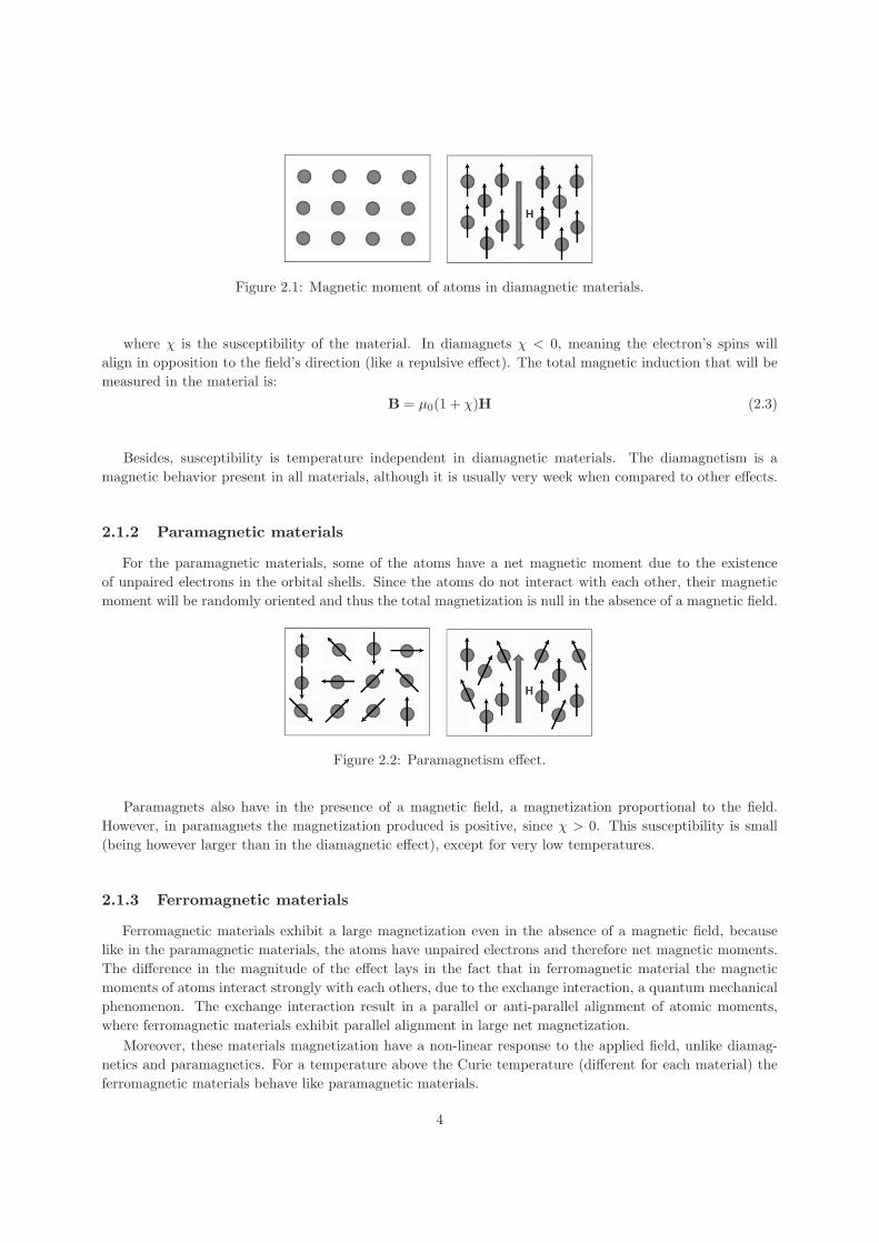
Figure 2.1: Magnetic moment of atoms in diamagnetic materials.
where χ is the susceptibility of the material. In diamagnets χ < 0, meaning the electron’s spins will
align in opposition to the field’s direction (like a repulsive effect). The total magnetic induction that will be
measured in the material is:
B = μ0(1 + χ)H (2.3)
Besides, susceptibility is temperature independent in diamagnetic materials. The diamagnetism is a
magnetic behavior present in all materials, although it is usually very week when compared to other effects.
2.1.2 Paramagnetic materials
For the paramagnetic materials, some of the atoms have a net magnetic moment due to the existence
of unpaired electrons in the orbital shells. Since the atoms do not interact with each other, their magnetic
moment will be randomly oriented and thus the total magnetization is null in the absence of a magnetic field.
Figure 2.2: Paramagnetism effect.
Paramagnets also have in the presence of a magnetic field, a magnetization proportional to the field.
However, in paramagnets the magnetization produced is positive, since χ > 0. This susceptibility is small
(being however larger than in the diamagnetic effect), except for very low temperatures.
2.1.3 Ferromagnetic materials
Ferromagnetic materials exhibit a large magnetization even in the absence of a magnetic field, because
like in the paramagnetic materials, the atoms have unpaired electrons and therefore net magnetic moments.
The difference in the magnitude of the effect lays in the fact that in ferromagnetic material the magnetic
moments of atoms interact strongly with each others, due to the exchange interaction, a quantum mechanical
phenomenon. The exchange interaction result in a parallel or anti-parallel alignment of atomic moments,
where ferromagnetic materials exhibit parallel alignment in large net magnetization.
Moreover, these materials magnetization have a non-linear response to the applied field, unlike diamag-
netics and paramagnetics. For a temperature above the Curie temperature (different for each material) the
ferromagnetic materials behave like paramagnetic materials.
4
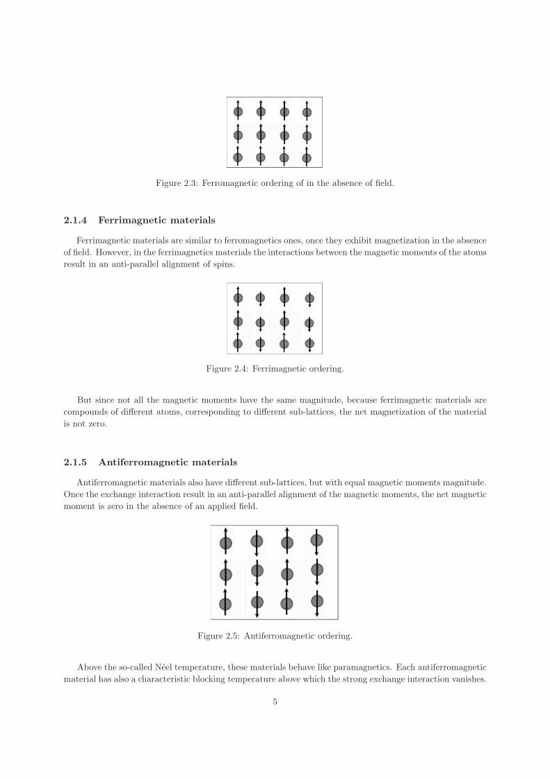
Figure 2.3: Ferromagnetic ordering of in the absence of field.
2.1.4 Ferrimagnetic materials
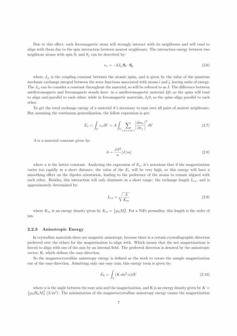
Ferrimagnetic materials are similar to ferromagnetics ones, once they exhibit magnetization in the absence
of field. However, in the ferrimagnetics materials the interactions between the magnetic moments of the atoms
result in an anti-parallel alignment of spins.
Figure 2.4: Ferrimagnetic ordering.
But since not all the magnetic moments have the same magnitude, because ferrimagnetic materials are
compounds of different atoms, corresponding to different sub-lattices, the net magnetization of the material
is not zero.
2.1.5 Antiferromagnetic materials
Antiferromagnetic materials also have different sub-lattices, but with equal magnetic moments magnitude.
Once the exchange interaction result in an anti-parallel alignment of the magnetic moments, the net magnetic
moment is zero in the absence of an applied field.
Figure 2.5: Antiferromagnetic ordering.
Above the so-called Neel temperature, these materials behave like paramagnetics. Each antiferromagnetic
material has also a characteristic blocking temperature above which the strong exchange interaction vanishes.
5

2.2 Micromagnetism for ferromagnetic materials
To describe the magnetic behavior of a ferromagnet the equation2.3 is not enough, since they exhibit a
magnetization (magnetic moment per unit of volume) even in the absence of an applied field. So becomes
necessary to take into account quantum mechanical mechanisms to fully explain ferromagnetism. The simplest
model assumes that the atoms or molecules that constitute the basis of a ferromagnetic material as punctual
dipoles, since they exhibit a certain permanent magnetic moment μ [13].
This moment existent in ferromagnets can be explained by the fact that in these material some of their
outer orbitals have a certain gap between the energy levels available for spin up and spin down electrons,
originating an unbalance between the number of electrons of the two spins. This difference between different
spins, averaged over the entire ferromagnetic volume, will origin a spontaneous magnetization. When a
magnetic field is applied the magnetic dipoles will assume the direction which minimizes the system energy.
So to describe the magnetic properties of a ferromagnet it’s necessary to take into consideration the effect of
several energy terms:
1. Zeeman Energy: describes the interaction with the external field
2. Exchange Energy: results from the quantum mechanical interactions between the magnetic dipoles of
the material
3. Anisotropic Energy: defined by the crystalline anisotropy of the material
4. Demagnetizing or Magnetostatic Energy: caused by the magnetic charges induced in the borders of a
magnetized body
5. Neel Energy: related to the conformal roughness of the ferromagnetic interfaces
2.2.1 Zeeman Energy
When an external field is applied to a dipole, it will align with the direction of the applied field. The
Zeeman energy is the energy related to this interaction between the applied field and the magnetization of
the material. It’s defined by the amount of work necessary to rotate the spin vector of an angle θ with the
direction of the applied field, and is given by:
eZ = −μ ·H = −μH cos θ (2.4)
If we now consider a sample of volume V with N atoms (assuming N large enough) the overall Zeeman
energy is the given by:
EZ = −μ0
∫V
M ·HdV (2.5)
This energy term is minimized when the magnetization is fully aligned with the applied field.
2.2.2 Exchange Energy
The exchange interaction is a quantum effect responsible for the types of spontaneous ordering of atomic
magnetic moments occurring in ferromagnets, antiferromagnets and ferrimagnets. This interaction is inde-
pendent of the direction of the total magnetic moment of the sample.
6
Due to this effect, each ferromagnetic atom will strongly interact with its neighbours and will tend to
align with them due to the spin interaction between nearest neighbours. The interaction energy between two
neighbour atoms with spin Si and Sj can be described by:
ex = −2JijSi · Sj (2.6)
where Jij is the coupling constant between the atomic spins, and is given by the value of the quantum
mechanic exchange integral between the wave functions associated with atoms i and j, having units of energy.
The Jij can be consider a constant throughout the material, so will be referred to as J. The difference between
antiferromagnets and ferromagnets stands here: in a antiferromagnetic material J¡0, so the spins will tend
to align anti-parallel to each other; while in ferromagnetic materials, J¿0, so the spins align parallel to each
other.
To get the total exchange energy of a material it’s necessary to sum over all pairs of nearest neighbours.
But assuming the continuum generalization, the follow expression is get:
Ex =
∫V
exdV = A
∫V
∑i,j=x,y,z
∣∣∣∣∂mi
∂rj
∣∣∣∣2
dV (2.7)
A is a material constant given by:
A =JS2
a[J/m] (2.8)
where a is the lattice constant. Analyzing the expression of Ex, it’s notorious that if the magnetization
varies too rapidly in a short distance, the value of the Ex will be very high, so this energy will have a
smoothing effect on the dipoles orientation, leading to the preference of the atoms to remain aligned with
each other. Besides, this interaction will only dominate in a short range: the exchange length Lex, and is
approximately determined by:
Lex =
√A
Km(2.9)
where Km is an energy density given by Km = 12μ0M
2S . For a NiFe permalloy, this length is the order of
nm.
2.2.3 Anisotropic Energy
In crystalline materials there are magnetic anisotropy, because there is a certain crystallographic direction
preferred over the others for the magnetization to align with. Which means that the net magnetizations is
forced to align with one of the axis by an internal field. The preferred direction is denoted by the anisotropic
vector, K, which defines the easy-direction.
So the magnetocrystalline anisotropy energy is defined as the work to rotate the sample magnetization
out of the easy-direction. Admitting only one easy axis, this energy term is given by:
Ek =
∫V
(K sin2 α)dV (2.10)
where α is the angle between the easy axis and the magnetization, and K is an energy density given byK =12μ0HkM
fS (J/m2). The minimization of the magnetocrystalline anisotropy energy causes the magnetization
7
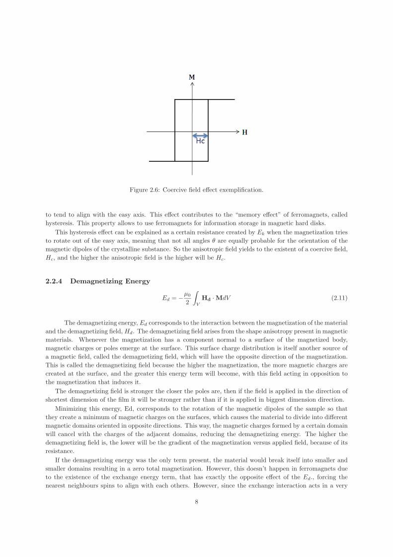
Figure 2.6: Coercive field effect exemplification.
to tend to align with the easy axis. This effect contributes to the “memory effect” of ferromagnets, called
hysteresis. This property allows to use ferromagnets for information storage in magnetic hard disks.
This hysteresis effect can be explained as a certain resistance created by Ek when the magnetization tries
to rotate out of the easy axis, meaning that not all angles θ are equally probable for the orientation of the
magnetic dipoles of the crystalline substance. So the anisotropic field yields to the existent of a coercive field,
Hc, and the higher the anisotropic field is the higher will be Hc.
2.2.4 Demagnetizing Energy
Ed = −μ0
2
∫V
Hd ·MdV (2.11)
The demagnetizing energy, Ed corresponds to the interaction between the magnetization of the material
and the demagnetizing field, Hd. The demagnetizing field arises from the shape anisotropy present in magnetic
materials. Whenever the magnetization has a component normal to a surface of the magnetized body,
magnetic charges or poles emerge at the surface. This surface charge distribution is itself another source of
a magnetic field, called the demagnetizing field, which will have the opposite direction of the magnetization.
This is called the demagnetizing field because the higher the magnetization, the more magnetic charges are
created at the surface, and the greater this energy term will become, with this field acting in opposition to
the magnetization that induces it.
The demagnetizing field is stronger the closer the poles are, then if the field is applied in the direction of
shortest dimension of the film it will be stronger rather than if it is applied in biggest dimension direction.
Minimizing this energy, Ed, corresponds to the rotation of the magnetic dipoles of the sample so that
they create a minimum of magnetic charges on the surfaces, which causes the material to divide into different
magnetic domains oriented in opposite directions. This way, the magnetic charges formed by a certain domain
will cancel with the charges of the adjacent domains, reducing the demagnetizing energy. The higher the
demagnetizing field is, the lower will be the gradient of the magnetization versus applied field, because of its
resistance.
If the demagnetizing energy was the only term present, the material would break itself into smaller and
smaller domains resulting in a zero total magnetization. However, this doesn’t happen in ferromagnets due
to the existence of the exchange energy term, that has exactly the opposite effect of the Ed., forcing the
nearest neighbours spins to align with each others. However, since the exchange interaction acts in a very
8
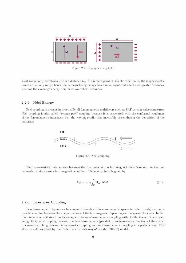
Figure 2.7: Demagnetizing field.
short range, only the atoms within a distance Lex will remain parallel. On the other hand, the magnetostatic
forces are of long range, hence the demagnetizing energy has a more significant effect over greater distances,
whereas the exchange energy dominates over short distances.
2.2.5 Neel Energy
Neel coupling is present in practically all ferromagnetic multilayers such as SAF or spin valve structures.
Neel coupling is also called “orange peel” coupling because it is associated with the conformal roughness
of the ferromagnetic interfaces, i.e., the waving profile that inevitably arises during the deposition of the
materials.
Figure 2.8: Neel coupling.
The magnetostatic interactions between the free poles at the ferromagnetic interfaces next to the non
magnetic barrier cause a ferromagnetic coupling. Neel energy term is given by:
EN = −μ0
∫V
Hn ·MdV (2.12)
2.2.6 Interlayer Coupling
Two ferromagnetic layers can be coupled through a thin non-magnetic spacer in order to origin an anti-
parallel coupling between the magnetizations of the ferromagnets, depending on the spacer thickness. In fact
the interaction oscillates from ferromagnetic to anti-ferromagnetic coupling with the thickness of the spacer,
being the type of coupling between the two ferromagnets (parallel or anti-parallel) a function of the spacer
thickness, switching between ferromagnetic coupling and antiferromagnetic coupling in a periodic way. This
effect is well described by the Ruderman-Kittel-Kasuya-Yodsida (RKKY) model.
9
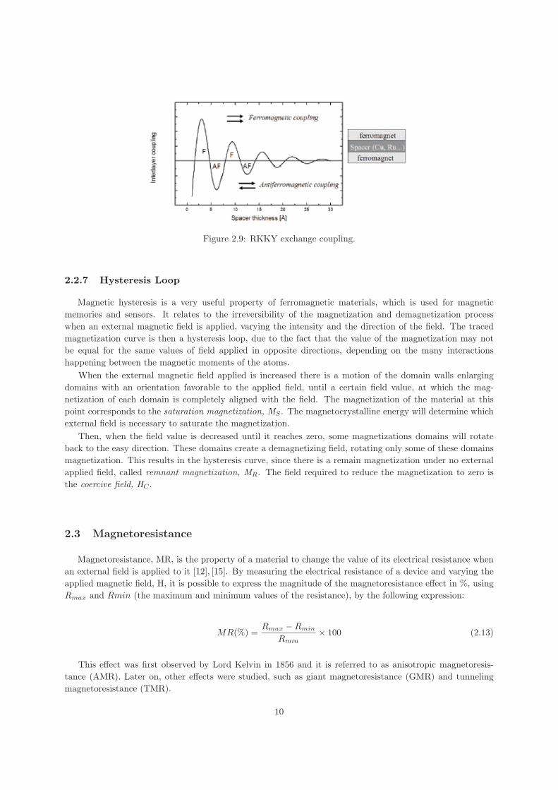
Figure 2.9: RKKY exchange coupling.
2.2.7 Hysteresis Loop
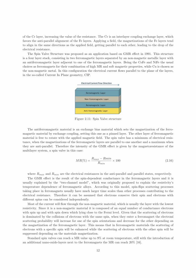
Magnetic hysteresis is a very useful property of ferromagnetic materials, which is used for magnetic
memories and sensors. It relates to the irreversibility of the magnetization and demagnetization process
when an external magnetic field is applied, varying the intensity and the direction of the field. The traced
magnetization curve is then a hysteresis loop, due to the fact that the value of the magnetization may not
be equal for the same values of field applied in opposite directions, depending on the many interactions
happening between the magnetic moments of the atoms.
When the external magnetic field applied is increased there is a motion of the domain walls enlarging
domains with an orientation favorable to the applied field, until a certain field value, at which the mag-
netization of each domain is completely aligned with the field. The magnetization of the material at this
point corresponds to the saturation magnetization, MS . The magnetocrystalline energy will determine which
external field is necessary to saturate the magnetization.
Then, when the field value is decreased until it reaches zero, some magnetizations domains will rotate
back to the easy direction. These domains create a demagnetizing field, rotating only some of these domains
magnetization. This results in the hysteresis curve, since there is a remain magnetization under no external
applied field, called remnant magnetization, MR. The field required to reduce the magnetization to zero is
the coercive field, HC .
2.3 Magnetoresistance
Magnetoresistance, MR, is the property of a material to change the value of its electrical resistance when
an external field is applied to it [12], [15]. By measuring the electrical resistance of a device and varying the
applied magnetic field, H, it is possible to express the magnitude of the magnetoresistance effect in %, using
Rmax and Rmin (the maximum and minimum values of the resistance), by the following expression:
MR(%) =Rmax −Rmin
Rmin× 100 (2.13)
This effect was first observed by Lord Kelvin in 1856 and it is referred to as anisotropic magnetoresis-
tance (AMR). Later on, other effects were studied, such as giant magnetoresistance (GMR) and tunneling
magnetoresistance (TMR).
10
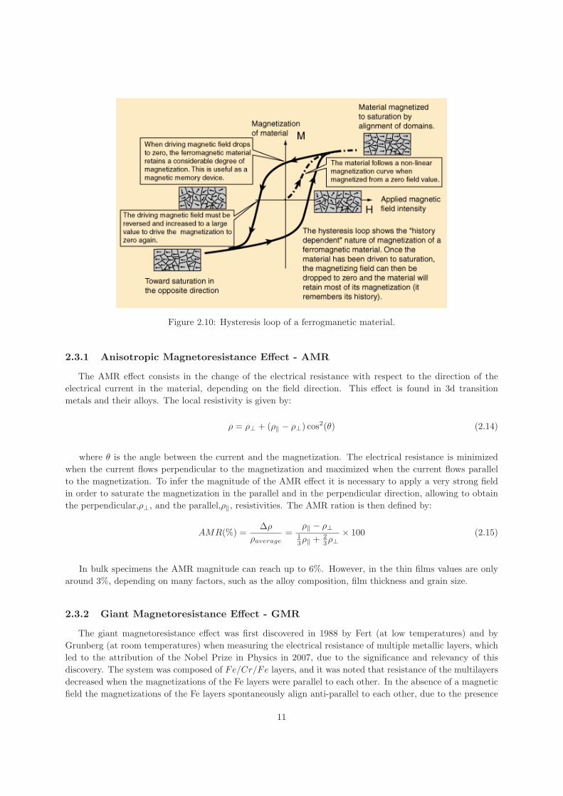
Figure 2.10: Hysteresis loop of a ferrogmanetic material.
2.3.1 Anisotropic Magnetoresistance Effect - AMR
The AMR effect consists in the change of the electrical resistance with respect to the direction of the
electrical current in the material, depending on the field direction. This effect is found in 3d transition
metals and their alloys. The local resistivity is given by:
ρ = ρ⊥ + (ρ‖ − ρ⊥) cos2(θ) (2.14)
where θ is the angle between the current and the magnetization. The electrical resistance is minimized
when the current flows perpendicular to the magnetization and maximized when the current flows parallel
to the magnetization. To infer the magnitude of the AMR effect it is necessary to apply a very strong field
in order to saturate the magnetization in the parallel and in the perpendicular direction, allowing to obtain
the perpendicular,ρ⊥, and the parallel,ρ‖, resistivities. The AMR ration is then defined by:
AMR(%) =Δρ
ρaverage=
ρ‖ − ρ⊥13ρ‖ +
23ρ⊥
× 100 (2.15)
In bulk specimens the AMR magnitude can reach up to 6%. However, in the thin films values are only
around 3%, depending on many factors, such as the alloy composition, film thickness and grain size.
2.3.2 Giant Magnetoresistance Effect - GMR
The giant magnetoresistance effect was first discovered in 1988 by Fert (at low temperatures) and by
Grunberg (at room temperatures) when measuring the electrical resistance of multiple metallic layers, which
led to the attribution of the Nobel Prize in Physics in 2007, due to the significance and relevancy of this
discovery. The system was composed of Fe/Cr/Fe layers, and it was noted that resistance of the multilayers
decreased when the magnetizations of the Fe layers were parallel to each other. In the absence of a magnetic
field the magnetizations of the Fe layers spontaneously align anti-parallel to each other, due to the presence
11
of the Cr layer, increasing the value of the resistance. The Cr is an interlayer coupling exchange layer, which
favors the anti-parallel alignment of the Fe layers. Applying a field, the magnetizations of the Fe layers tend
to align in the same directions as the applied field, getting parallel to each other, leading to the drop of the
electrical resistance.
The Spin Valve Structure was proposed as an application based on GMR effect in 1991. This structure
is a four layer stack, consisting in two ferromagnetic layers separated by an non-magnetic metallic layer with
an antiferromagnetic layer adjacent to one of the ferromagnetic layers. Being the CoFe and NiFe the usual
choices as ferromagnets for their combination of high MR and soft magnetic properties, while Cu is chosen as
the non-magnetic metal. In this configuration the electrical current flows parallel to the plane of the layers,
in the so-called Current In Plane geometry, CIP.
Figure 2.11: Spin Valve structure
The antiferromagnetic material is an exchange bias material which sets the magnetization of the ferro-
magnetic material by exchange coupling, setting this one as a pinned layer. The other layer of ferromagnetic
material is free to rotate with the applied magnetic field. The spin valve has a minimum of electrical resis-
tance, when the magnetizations of the ferromagnetic layers are parallel to one another and a maximum when
they are anti-parallel. Therefore the intensity of the GMR effect is given by the magnetoresistance of the
multilayer system, a spin valve in this case:
MR(%) =Rmax −Rmin
Rmin× 100 (2.16)
where Rmax and Rmin are the electrical resistances in the anti-parallel and parallel states, respectively.
The GMR effect is the result of the spin-dependent conductance in the ferromagnetic layers and it is
usually explained by the “two-channel model”, which was originally proposed to explain the resistivity’s
temperature dependence of ferromagnetic alloys. According to this model, spin-flips scattering processes
taking place in ferromagnets usually have much larger time scales than other processes contributing to the
electrical resistance. Therefore it can be assumed that electrons conserve their spin and electrons with
different spins can be considered independently.
Most of the current will flow through the non-magnetic material, which is usually the layer with the lowest
resistivity. Since it is a non-magnetic material it is composed of an equal number of conductance electrons
with spin up and with spin down which lying close to the Fermi level. Given that the scattering of electrons
is dominated by the collisions of electrons with the same spin, when they enter a ferromagnet the electrons
scattering probability will increase for one of the spin orientations and decrease for the other depending on
the magnetization of the ferromagnetic layer. This means that in ferromagnetic materials the scattering of
electrons with a specific spin will be enhanced while the scattering of electrons with the other spin will be
suppressed depending on the materials magnetization.
Standard spin valves can reach a MR value up to 9% at room temperature, still with the introduction of
an additional nano-oxide-layers next to the ferromagnets the MR can reach 20% [16].
12
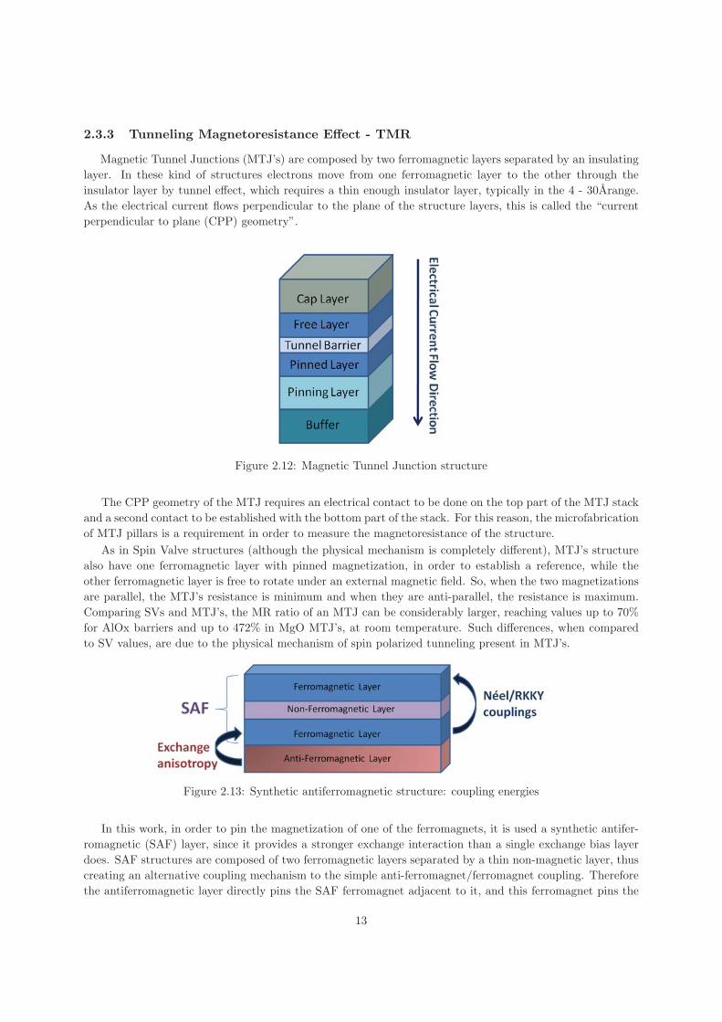
2.3.3 Tunneling Magnetoresistance Effect - TMR
Magnetic Tunnel Junctions (MTJ’s) are composed by two ferromagnetic layers separated by an insulating
layer. In these kind of structures electrons move from one ferromagnetic layer to the other through the
insulator layer by tunnel effect, which requires a thin enough insulator layer, typically in the 4 - 30Arange.
As the electrical current flows perpendicular to the plane of the structure layers, this is called the “current
perpendicular to plane (CPP) geometry”.
Figure 2.12: Magnetic Tunnel Junction structure
The CPP geometry of the MTJ requires an electrical contact to be done on the top part of the MTJ stack
and a second contact to be established with the bottom part of the stack. For this reason, the microfabrication
of MTJ pillars is a requirement in order to measure the magnetoresistance of the structure.
As in Spin Valve structures (although the physical mechanism is completely different), MTJ’s structure
also have one ferromagnetic layer with pinned magnetization, in order to establish a reference, while the
other ferromagnetic layer is free to rotate under an external magnetic field. So, when the two magnetizations
are parallel, the MTJ’s resistance is minimum and when they are anti-parallel, the resistance is maximum.
Comparing SVs and MTJ’s, the MR ratio of an MTJ can be considerably larger, reaching values up to 70%
for AlOx barriers and up to 472% in MgO MTJ’s, at room temperature. Such differences, when compared
to SV values, are due to the physical mechanism of spin polarized tunneling present in MTJ’s.
Figure 2.13: Synthetic antiferromagnetic structure: coupling energies
In this work, in order to pin the magnetization of one of the ferromagnets, it is used a synthetic antifer-
romagnetic (SAF) layer, since it provides a stronger exchange interaction than a single exchange bias layer
does. SAF structures are composed of two ferromagnetic layers separated by a thin non-magnetic layer, thus
creating an alternative coupling mechanism to the simple anti-ferromagnet/ferromagnet coupling. Therefore
the antiferromagnetic layer directly pins the SAF ferromagnet adjacent to it, and this ferromagnet pins the
13
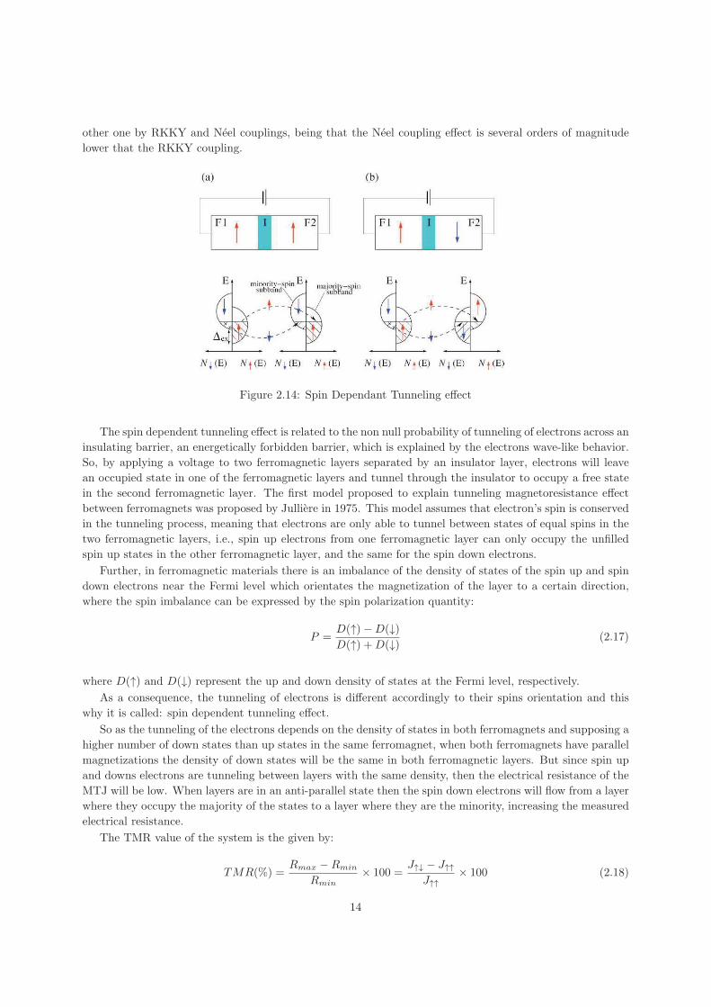
other one by RKKY and Neel couplings, being that the Neel coupling effect is several orders of magnitude
lower that the RKKY coupling.
Figure 2.14: Spin Dependant Tunneling effect
The spin dependent tunneling effect is related to the non null probability of tunneling of electrons across an
insulating barrier, an energetically forbidden barrier, which is explained by the electrons wave-like behavior.
So, by applying a voltage to two ferromagnetic layers separated by an insulator layer, electrons will leave
an occupied state in one of the ferromagnetic layers and tunnel through the insulator to occupy a free state
in the second ferromagnetic layer. The first model proposed to explain tunneling magnetoresistance effect
between ferromagnets was proposed by Julliere in 1975. This model assumes that electron’s spin is conserved
in the tunneling process, meaning that electrons are only able to tunnel between states of equal spins in the
two ferromagnetic layers, i.e., spin up electrons from one ferromagnetic layer can only occupy the unfilled
spin up states in the other ferromagnetic layer, and the same for the spin down electrons.
Further, in ferromagnetic materials there is an imbalance of the density of states of the spin up and spin
down electrons near the Fermi level which orientates the magnetization of the layer to a certain direction,
where the spin imbalance can be expressed by the spin polarization quantity:
P =D(↑)−D(↓)D(↑) +D(↓) (2.17)
where D(↑) and D(↓) represent the up and down density of states at the Fermi level, respectively.
As a consequence, the tunneling of electrons is different accordingly to their spins orientation and this
why it is called: spin dependent tunneling effect.
So as the tunneling of the electrons depends on the density of states in both ferromagnets and supposing a
higher number of down states than up states in the same ferromagnet, when both ferromagnets have parallel
magnetizations the density of down states will be the same in both ferromagnetic layers. But since spin up
and downs electrons are tunneling between layers with the same density, then the electrical resistance of the
MTJ will be low. When layers are in an anti-parallel state then the spin down electrons will flow from a layer
where they occupy the majority of the states to a layer where they are the minority, increasing the measured
electrical resistance.
The TMR value of the system is the given by:
TMR(%) =Rmax −Rmin
Rmin× 100 =
J↑↓ − J↑↑J↑↑
× 100 (2.18)
14
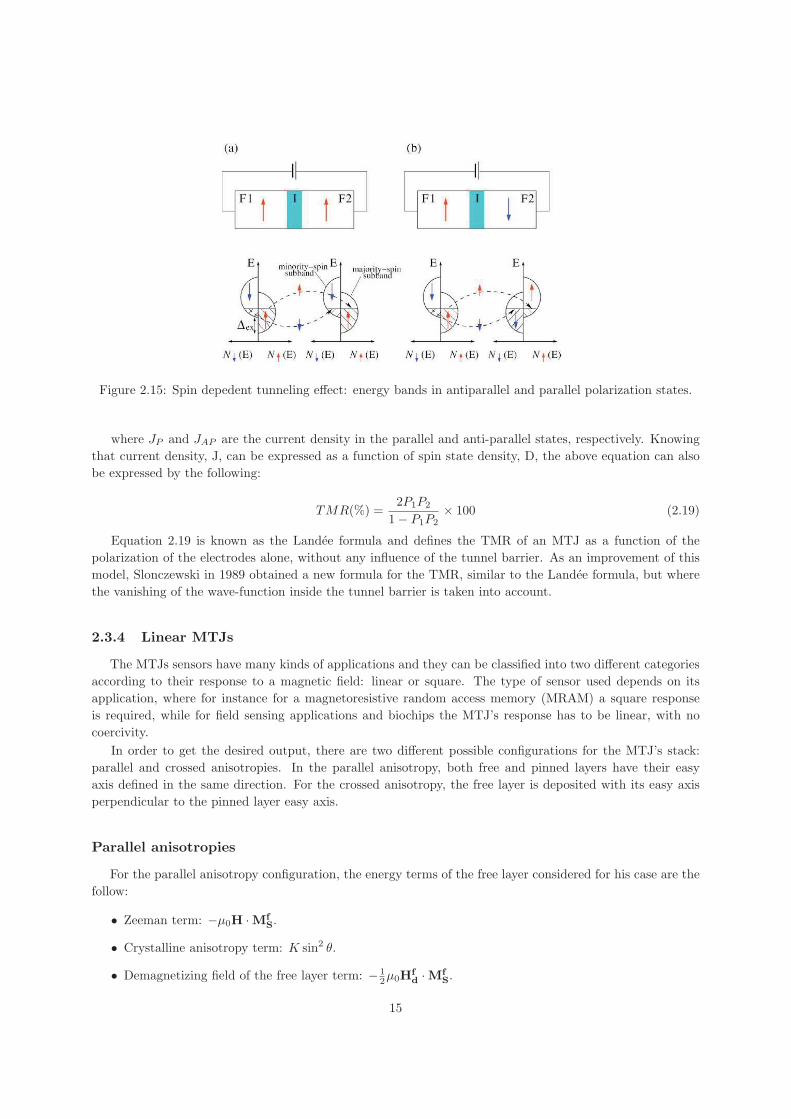
Figure 2.15: Spin depedent tunneling effect: energy bands in antiparallel and parallel polarization states.
where JP and JAP are the current density in the parallel and anti-parallel states, respectively. Knowing
that current density, J, can be expressed as a function of spin state density, D, the above equation can also
be expressed by the following:
TMR(%) =2P1P2
1− P1P2× 100 (2.19)
Equation 2.19 is known as the Landee formula and defines the TMR of an MTJ as a function of the
polarization of the electrodes alone, without any influence of the tunnel barrier. As an improvement of this
model, Slonczewski in 1989 obtained a new formula for the TMR, similar to the Landee formula, but where
the vanishing of the wave-function inside the tunnel barrier is taken into account.
2.3.4 Linear MTJs
The MTJs sensors have many kinds of applications and they can be classified into two different categories
according to their response to a magnetic field: linear or square. The type of sensor used depends on its
application, where for instance for a magnetoresistive random access memory (MRAM) a square response
is required, while for field sensing applications and biochips the MTJ’s response has to be linear, with no
coercivity.
In order to get the desired output, there are two different possible configurations for the MTJ’s stack:
parallel and crossed anisotropies. In the parallel anisotropy, both free and pinned layers have their easy
axis defined in the same direction. For the crossed anisotropy, the free layer is deposited with its easy axis
perpendicular to the pinned layer easy axis.
Parallel anisotropies
For the parallel anisotropy configuration, the energy terms of the free layer considered for his case are the
follow:
• Zeeman term: −μ0H ·MfS.
• Crystalline anisotropy term: K sin2 θ.
• Demagnetizing field of the free layer term: − 12μ0H
fd ·Mf
S.
15
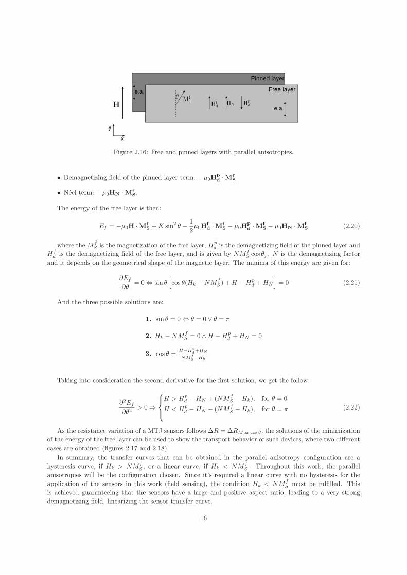
Figure 2.16: Free and pinned layers with parallel anisotropies.
• Demagnetizing field of the pinned layer term: −μ0Hpd ·Mf
S.
• Neel term: −μ0HN ·MfS.
The energy of the free layer is then:
Ef = −μ0H ·MfS +K sin2 θ − 1
2μ0H
fd ·Mf
S − μ0Hpd ·Mf
S − μ0HN ·MfS (2.20)
where the MfS is the magnetization of the free layer, Hp
d is the demagnetizing field of the pinned layer and
Hfd is the demagnetizing field of the free layer, and is given by NMf
S cos θj . N is the demagnetizing factor
and it depends on the geometrical shape of the magnetic layer. The minima of this energy are given for:
∂Ef
∂θ= 0 ⇔ sin θ
[cos θ(Hk −NMf
S ) +H −Hpd +HN
]= 0 (2.21)
And the three possible solutions are:
1. sin θ = 0 ⇔ θ = 0 ∨ θ = π
2. Hk −NMfS = 0 ∧H −Hp
d +HN = 0
3. cos θ =H−Hp
d+HN
NMfS−Hk
Taking into consideration the second derivative for the first solution, we get the follow:
∂2Ef
∂θ2> 0 ⇒
⎧⎪⎨⎪⎩H > Hp
d −HN + (NMfS −Hk), for θ = 0
H < Hpd −HN − (NMf
S −Hk), for θ = π (2.22)
As the resistance variation of a MTJ sensors follows ΔR = ΔRMax cos θ, the solutions of the minimization
of the energy of the free layer can be used to show the transport behavior of such devices, where two different
cases are obtained (figures 2.17 and 2.18).
In summary, the transfer curves that can be obtained in the parallel anisotropy configuration are a
hysteresis curve, if Hk > NMfS , or a linear curve, if Hk < NMf
S . Throughout this work, the parallel
anisotropies will be the configuration chosen. Since it’s required a linear curve with no hysteresis for the
application of the sensors in this work (field sensing), the condition Hk < NMfS must be fulfilled. This
is achieved guaranteeing that the sensors have a large and positive aspect ratio, leading to a very strong
demagnetizing field, linearizing the sensor transfer curve.
16
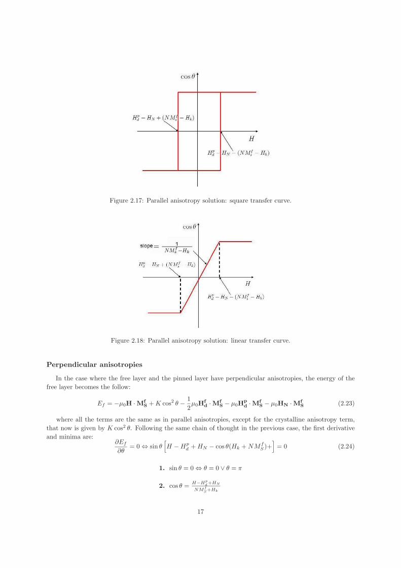
Figure 2.17: Parallel anisotropy solution: square transfer curve.
Figure 2.18: Parallel anisotropy solution: linear transfer curve.
Perpendicular anisotropies
In the case where the free layer and the pinned layer have perpendicular anisotropies, the energy of the
free layer becomes the follow:
Ef = −μ0H ·MfS +K cos2 θ − 1
2μ0H
fd ·Mf
S − μ0Hpd ·Mf
S − μ0HN ·MfS (2.23)
where all the terms are the same as in parallel anisotropies, except for the crystalline anisotropy term,
that now is given by K cos2 θ. Following the same chain of thought in the previous case, the first derivative
and minima are:∂Ef
∂θ= 0 ⇔ sin θ
[H −Hp
d +HN − cos θ(Hk +NMfS )+
]= 0 (2.24)
1. sin θ = 0 ⇔ θ = 0 ∨ θ = π
2. cos θ =H−Hp
d+HN
NMfS+Hk
17

Figure 2.19: Free and pinned layers with perpendicular anisotropies.
Where the second derivative taking into consideration the first solution is:
∂2Ef
∂θ2> 0 ⇒
⎧⎪⎨⎪⎩H > Hp
d −HN + (NMfS +Hk), for θ = 0
H < Hpd −HN − (NMf
S +Hk), for θ = π (2.25)
So in the case of perpendicular anisotropies, the sensor transfer curve will always be linear (figure 2.20),
independently of the shape factors of the magnetic layers.
Figure 2.20: Crossed anisotropy solution: linear transfer curve.
18
Chapter 3
Experimental Facilities
3.1 Sputtering Deposition Systems
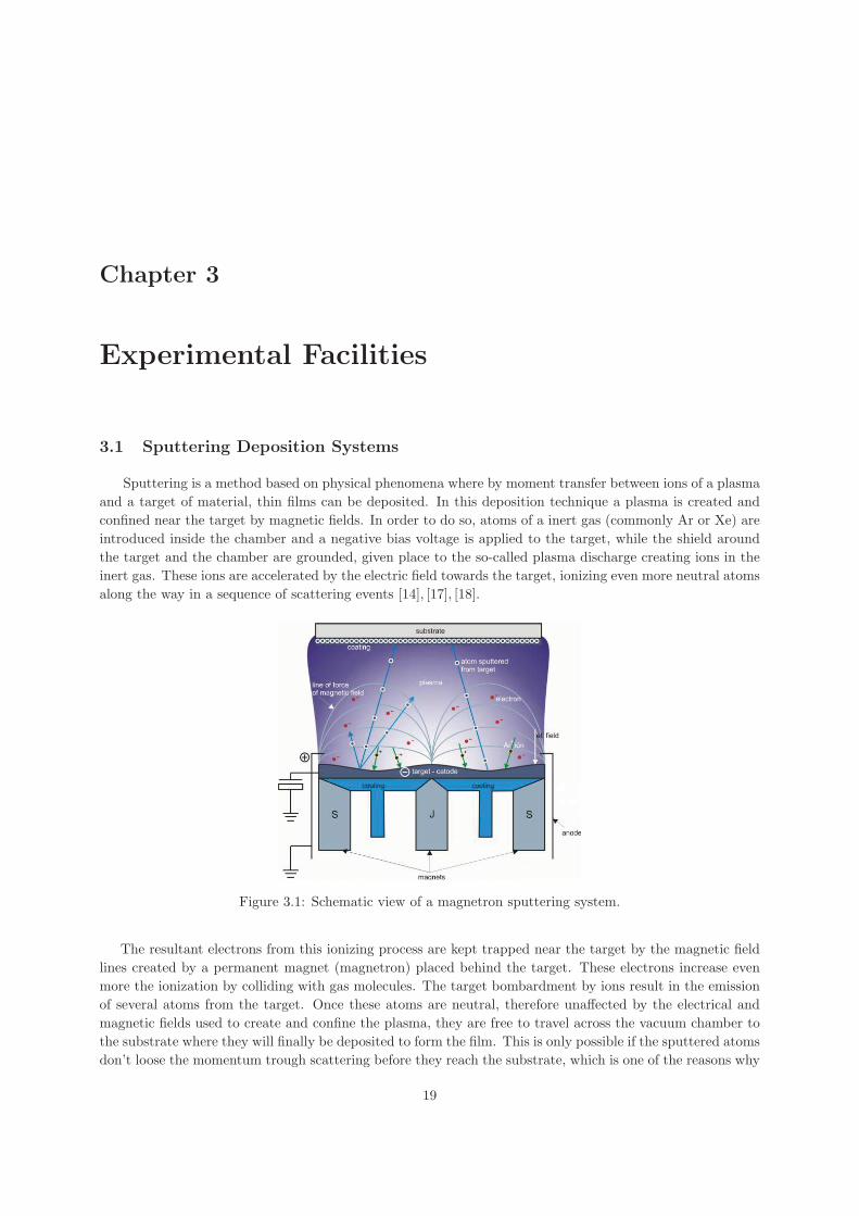
Sputtering is a method based on physical phenomena where by moment transfer between ions of a plasma
and a target of material, thin films can be deposited. In this deposition technique a plasma is created and
confined near the target by magnetic fields. In order to do so, atoms of a inert gas (commonly Ar or Xe) are
introduced inside the chamber and a negative bias voltage is applied to the target, while the shield around
the target and the chamber are grounded, given place to the so-called plasma discharge creating ions in the
inert gas. These ions are accelerated by the electric field towards the target, ionizing even more neutral atoms
along the way in a sequence of scattering events [14], [17], [18].
Figure 3.1: Schematic view of a magnetron sputtering system.
The resultant electrons from this ionizing process are kept trapped near the target by the magnetic field
lines created by a permanent magnet (magnetron) placed behind the target. These electrons increase even
more the ionization by colliding with gas molecules. The target bombardment by ions result in the emission
of several atoms from the target. Once these atoms are neutral, therefore unaffected by the electrical and
magnetic fields used to create and confine the plasma, they are free to travel across the vacuum chamber to
the substrate where they will finally be deposited to form the film. This is only possible if the sputtered atoms
don’t loose the momentum trough scattering before they reach the substrate, which is one of the reasons why
19
a vacuum chamber is required in the first place.
The target can be biased with a DC or a RF power supply, depending on the material to be deposited.
RF must be used with insulating materials as the charge of the incident ions cannot be neutralized, since
the material doesn′t allow current to flow and the accumulation of these ions in the target will repel the
incoming ions, interrupting this way the deposition. The substrate can either be grounded or connected to
a RF power supply. In the later case, the aim is attract ions from the plasma turning the substrate in a
target itself. This process can be used alone to remove deposited material from the sample or clean metallic
surfaces from oxide residues, in a process called sputter etching.
3.1.1 Nordiko 2000
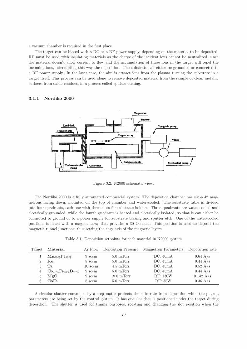
Figure 3.2: N2000 schematic view.
The Nordiko 2000 is a fully automated commercial system. The deposition chamber has six φ 4′′ mag-
netrons facing down, mounted on the top of chamber and water-cooled. The substrate table is divided
into four quadrants, each one with three slots for substrate-holders. Three quadrants are water-cooled and
electrically grounded, while the fourth quadrant is heated and electrically isolated, so that it can either be
connected to ground or to a power supply for substrate biasing and sputter etch. One of the water-cooled
positions is fitted with a magnet array that provides a 30 Oe field. This position is used to deposit the
magnetic tunnel junctions, thus setting the easy axis of the magnetic layers.
Table 3.1: Deposition setpoints for each material in N2000 system
Target Material Ar Flow Deposition Pressure Magnetron Parameters Depoisition rate
1. Mn60%Pt40% 9 sccm 5.0 mTorr DC: 40mA 0.64 A/s2. Ru 8 sccm 5.0 mTorr DC: 45mA 0.44 A/s3. Ta 10 sccm 4.5 mTorr DC: 45mA 0.52 A/s4. Co40%Fe40%B20% 9 sccm 5.0 mTorr DC: 45mA 0.44 A/s5. MgO 9 sccm 18.0 mTorr RF: 130W 0.142 A/s6. CoFe 8 sccm 5.0 mTorr RF: 35W 0.36 A/s
A circular shutter controlled by a step motor protects the substrate from deposition while the plasma
parameters are being set by the control system. It has one slot that is positioned under the target during
deposition. The shutter is used for timing purposes, rotating and changing the slot position when the
20

deposition time finishes, before the plasma is turned off. Samples are loaded through an automatic loadlock
into the round-shaped substrate table (12 stations). This facility is installed in a class 10000 clean room
and it was used for the deposition of the MTJ stack used during this work. The typical base pressure is
8− 9× 10⁻⁸ Torr.
3.1.2 Nordiko 7000
Figure 3.3: N7000: picture (left) and schematic view (right).
Nordiko 7000 is an automated system with four modules, a central dealer and a loadlock chamber, and it
is able to handle φ 6′′ wafers, that can be moved between modules by a robot arm. Each module can reach
a high-vacuum base pressure of 5× 10⁻⁹ Torr with a Cryogenic pump. Identically, in the dealer, a 2× 10⁻⁸
Torr pressure can be obtained. N7000 is installed in a class 100 cleanroom.
Table 3.2: Standart conditions of operation of the three modules of N7000 used during this work.
Module 2 RF1 RF2 Pressure Gas Flow Time
Soft Sputter Etch 70W 40W 3.0 mTorr 50 sccm Ar 1’
Module 3 DC Power Pressure Gas Flow Deposition Rate
TiW(N) 0.50 kW 3.0 mTorr 50 sccm Ar + 10 sccm N2 ∼5.56 A/s
Module 4 DC Power Pressure Gas Flow Deposition Rate
Al 2.0 kW 3.0 mTorr 50 sccm Ar ∼37.5 A/s
The four modules have different purposes, which are:
1. Module one consists in an array of lamps and it’s used for flash annealing.
21
2. Module two has a magnetron, which allows to use it to soft sputter etching processes. The soft etch is
used before the deposition of T iW (N) and AlSi1%Cu0.5%, in order to remove the oxide layer that is
naturally formed in metallic layers.
3. Module three is used for reactive sputtering deposition of T iW (N), where the material target is of
T iW and the N is obtained from the plasma, which is made of Ar and N2. T iW (N) is a material that
provides physical damage’s protection to the micro-structures and also protects Aluminum layers from
chemical substances. Moreover, it works as a anti-reflective coating in the optical lithography.
4. Module four is for AlSi1%Cu0.5% sputter deposition. This metal alloy is used as tunnel junction’s top
contact and as current paths, usually 3000A thicks.
3.1.3 UHV II
Figure 3.4: UHVII: front view picture (left) and side view schematic (right).
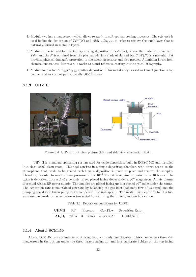
UHV II is a manual sputtering system used for oxide deposition, built in INESC-MN and installed
in a class 10000 clean room. This tool consists in a single deposition chamber, with direct access to the
atmosphere, that needs to be vented each time a deposition is made to place and remove the samples.
Therefore, in order to reach a base pressure of 3 × 10⁻⁷ Torr it is required a period of ∼ 10 hours. The
oxide is deposited from a Al2O3 ceramic target placed facing down under a φ6′′ magnetron. An Ar plasma
is created with a RF power supply. The samples are placed facing up in a cooled φ6′′ table under the target.
The deposition rate is maintained constant by balancing the gas inlet (constant flow of 45 sccm) and the
pumping speed (the turbo pump is set to operate in cruise speed). The oxide films deposited by this tool
were used as insulator layers between two metal layers during the tunnel junction fabrication.
Table 3.3: Deposition conditions for UHVII
UHVII RF Pressure Gas Flow Deposition Rate
AL2O3 200W 3.0 mTorr 45 sccm Ar 11.43A/min
3.1.4 Alcatel SCM450
Alcatel SCM 450 is a commercial sputtering tool, with only one chamber. This chamber has three φ4′′
magnetrons in the bottom under the three targets facing up, and four substrate holders on the top facing
22
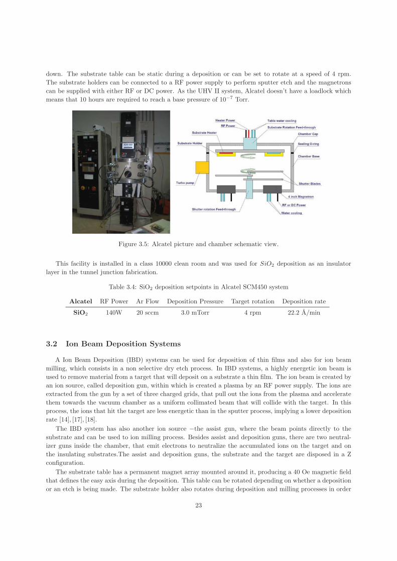
down. The substrate table can be static during a deposition or can be set to rotate at a speed of 4 rpm.
The substrate holders can be connected to a RF power supply to perform sputter etch and the magnetrons
can be supplied with either RF or DC power. As the UHV II system, Alcatel doesn’t have a loadlock which
means that 10 hours are required to reach a base pressure of 10−7 Torr.
Figure 3.5: Alcatel picture and chamber schematic view.
This facility is installed in a class 10000 clean room and was used for SiO2 deposition as an insulator
layer in the tunnel junction fabrication.
Table 3.4: SiO2 deposition setpoints in Alcatel SCM450 system
Alcatel RF Power Ar Flow Deposition Pressure Target rotation Deposition rate
SiO2 140W 20 sccm 3.0 mTorr 4 rpm 22.2 A/min
3.2 Ion Beam Deposition Systems
A Ion Beam Deposition (IBD) systems can be used for deposition of thin films and also for ion beam
milling, which consists in a non selective dry etch process. In IBD systems, a highly energetic ion beam is
used to remove material from a target that will deposit on a substrate a thin film. The ion beam is created by
an ion source, called deposition gun, within which is created a plasma by an RF power supply. The ions are
extracted from the gun by a set of three charged grids, that pull out the ions from the plasma and accelerate
them towards the vacuum chamber as a uniform collimated beam that will collide with the target. In this
process, the ions that hit the target are less energetic than in the sputter process, implying a lower deposition
rate [14], [17], [18].
The IBD system has also another ion source −the assist gun, where the beam points directly to the
substrate and can be used to ion milling process. Besides assist and deposition guns, there are two neutral-
izer guns inside the chamber, that emit electrons to neutralize the accumulated ions on the target and on
the insulating substrates.The assist and deposition guns, the substrate and the target are disposed in a Z
configuration.
The substrate table has a permanent magnet array mounted around it, producing a 40 Oe magnetic field
that defines the easy axis during the deposition. This table can be rotated depending on whether a deposition
or an etch is being made. The substrate holder also rotates during deposition and milling processes in order
23
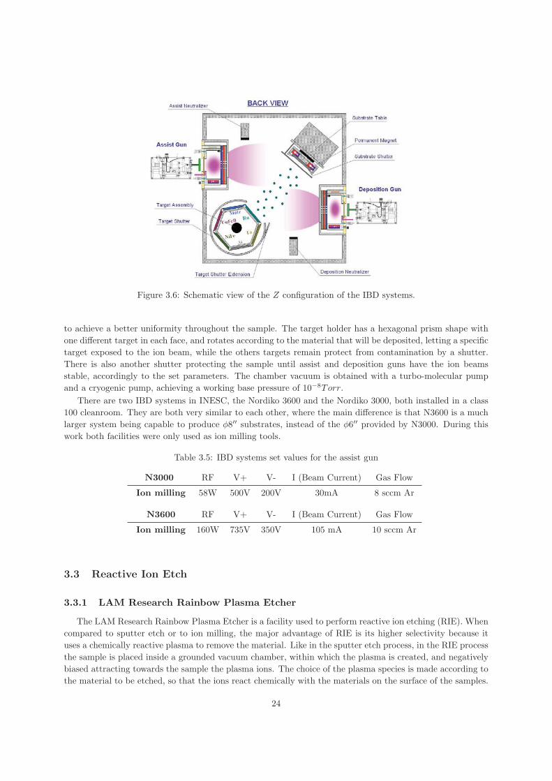
Figure 3.6: Schematic view of the Z configuration of the IBD systems.
to achieve a better uniformity throughout the sample. The target holder has a hexagonal prism shape with
one different target in each face, and rotates according to the material that will be deposited, letting a specific
target exposed to the ion beam, while the others targets remain protect from contamination by a shutter.
There is also another shutter protecting the sample until assist and deposition guns have the ion beams
stable, accordingly to the set parameters. The chamber vacuum is obtained with a turbo-molecular pump
and a cryogenic pump, achieving a working base pressure of 10−8Torr.
There are two IBD systems in INESC, the Nordiko 3600 and the Nordiko 3000, both installed in a class
100 cleanroom. They are both very similar to each other, where the main difference is that N3600 is a much
larger system being capable to produce φ8′′ substrates, instead of the φ6′′ provided by N3000. During this
work both facilities were only used as ion milling tools.
Table 3.5: IBD systems set values for the assist gun
N3000 RF V+ V- I (Beam Current) Gas Flow
Ion milling 58W 500V 200V 30mA 8 sccm Ar
N3600 RF V+ V- I (Beam Current) Gas Flow
Ion milling 160W 735V 350V 105 mA 10 sccm Ar
3.3 Reactive Ion Etch
3.3.1 LAM Research Rainbow Plasma Etcher
The LAM Research Rainbow Plasma Etcher is a facility used to perform reactive ion etching (RIE). When
compared to sputter etch or to ion milling, the major advantage of RIE is its higher selectivity because it
uses a chemically reactive plasma to remove the material. Like in the sputter etch process, in the RIE process
the sample is placed inside a grounded vacuum chamber, within which the plasma is created, and negatively
biased attracting towards the sample the plasma ions. The choice of the plasma species is made according to
the material to be etched, so that the ions react chemically with the materials on the surface of the samples.
24
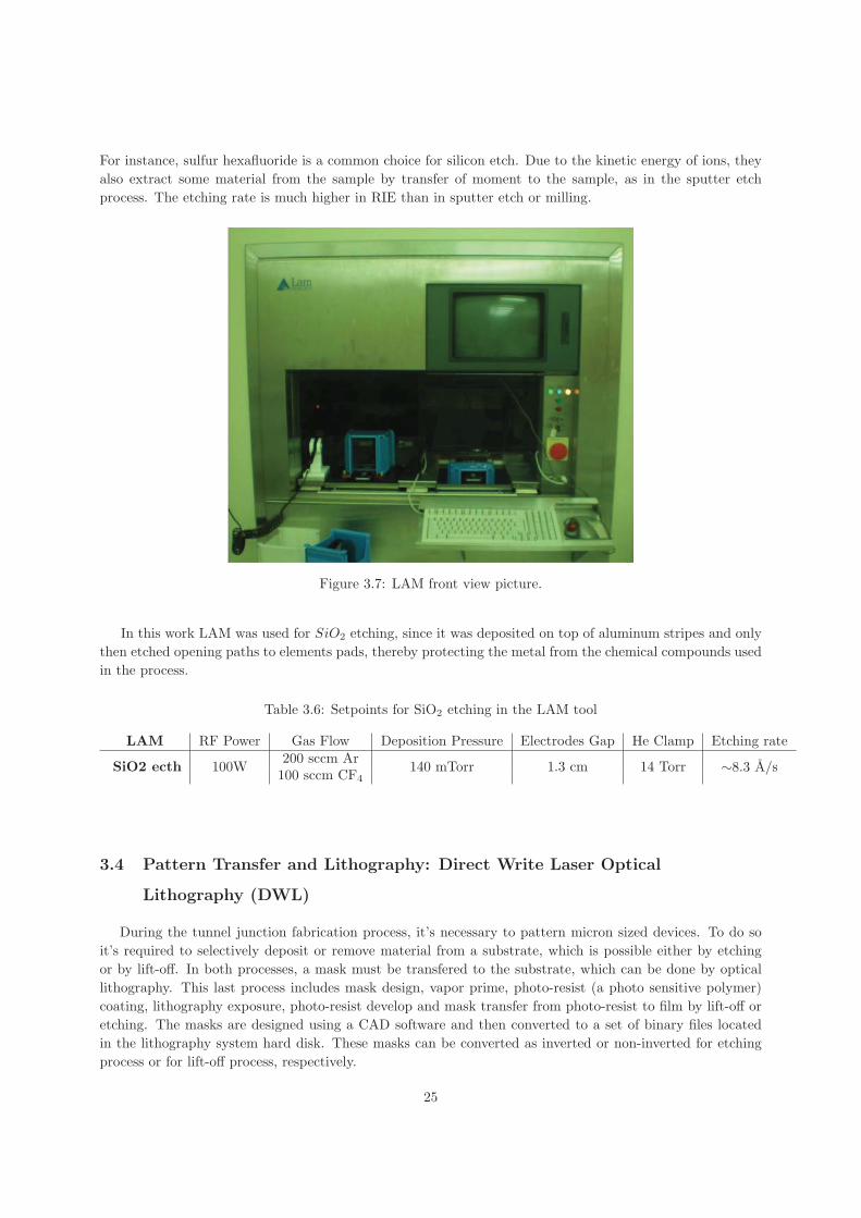
For instance, sulfur hexafluoride is a common choice for silicon etch. Due to the kinetic energy of ions, they
also extract some material from the sample by transfer of moment to the sample, as in the sputter etch
process. The etching rate is much higher in RIE than in sputter etch or milling.
Figure 3.7: LAM front view picture.
In this work LAM was used for SiO2 etching, since it was deposited on top of aluminum stripes and only
then etched opening paths to elements pads, thereby protecting the metal from the chemical compounds used
in the process.
Table 3.6: Setpoints for SiO2 etching in the LAM tool
LAM RF Power Gas Flow Deposition Pressure Electrodes Gap He Clamp Etching rate
SiO2 ecth 100W200 sccm Ar
140 mTorr 1.3 cm 14 Torr ∼8.3 A/s100 sccm CF4
3.4 Pattern Transfer and Lithography: Direct Write Laser Optical
Lithography (DWL)
During the tunnel junction fabrication process, it’s necessary to pattern micron sized devices. To do so
it’s required to selectively deposit or remove material from a substrate, which is possible either by etching
or by lift-off. In both processes, a mask must be transfered to the substrate, which can be done by optical
lithography. This last process includes mask design, vapor prime, photo-resist (a photo sensitive polymer)
coating, lithography exposure, photo-resist develop and mask transfer from photo-resist to film by lift-off or
etching. The masks are designed using a CAD software and then converted to a set of binary files located
in the lithography system hard disk. These masks can be converted as inverted or non-inverted for etching
process or for lift-off process, respectively.
25
3.4.1 Vapor Prime
Vapor prime improves photo-resist adhesion on sample surface and it’s made before coating the sample.
Basically, the vapor prime system consists in an vacuum oven within which the samples are placed and
submitted to a cycle (program 0):
1. Wafer dehydration and purge oxygen from the chamber: Vacuum, 10 Torr, 2 minutes
N2 inlet, 760 Torr, 3 minutes (3 times)
2. Priming: Vacuum, 1 Torr, 3 minutes
hexamethyldisilizane (HDMS), 6 Torr, 5 minutes
3. Purge prime exhaust: Vacuum, 4 Torr, 1 minute
N2 inlet, 500 Torr, 2 minutes
Vacuum, 4 Torr, 2 minutes
3.4.2 Photo-resist coating and developing
Figure 3.8: SVG tracks.
After the vapor prime, samples need to be coated with the photo-resist. There are two types of photo-
resist: positive (used during this work) and negative. The positive photo-resist is made of a resin and a
photoactive compound dissolved in a solvent that is also a dissolution inhibitor. This type of photo-resist has
a photo-reactive component which becomes unstable when exposed to light with a determined wavelength,
allowing to dissolve it by developing.
So, in the coating track, the samples are coated with 1.5μm positive photo-resist (PFR7790G27cP) and
after lithographic laser exposure, developed in the developer-track with Ethyl lactate (Pth70eg). The coating
and developing procedures are:
1. Coating - Recipe 6/2 :
• Dispense of photo-resist at 800rpm for 5s
• Spin at 2.8 krpm for 40s, then at 1.6 krpm for 5s
• Clean photo-resist from the wafer border at 1krpm for 2s
• Spin at 1.5 krpm for 15s
26
• Bake at 110◦C for 60s
2. Developing - Recipe 6/2 :
• Bake at 90◦C for 60s
• Cooling for 30s
• Water spray and rinse at 500rpm for 1s
• Dispense of developer at 500rpm for 5s
• Development for 60 s with the wafer stopped
• Rinse with DI water at 1 krpm for 20s
• Drying with wafer rotating at 3.5 krpm for 30s
3.4.3 Optical Lithography Exposure
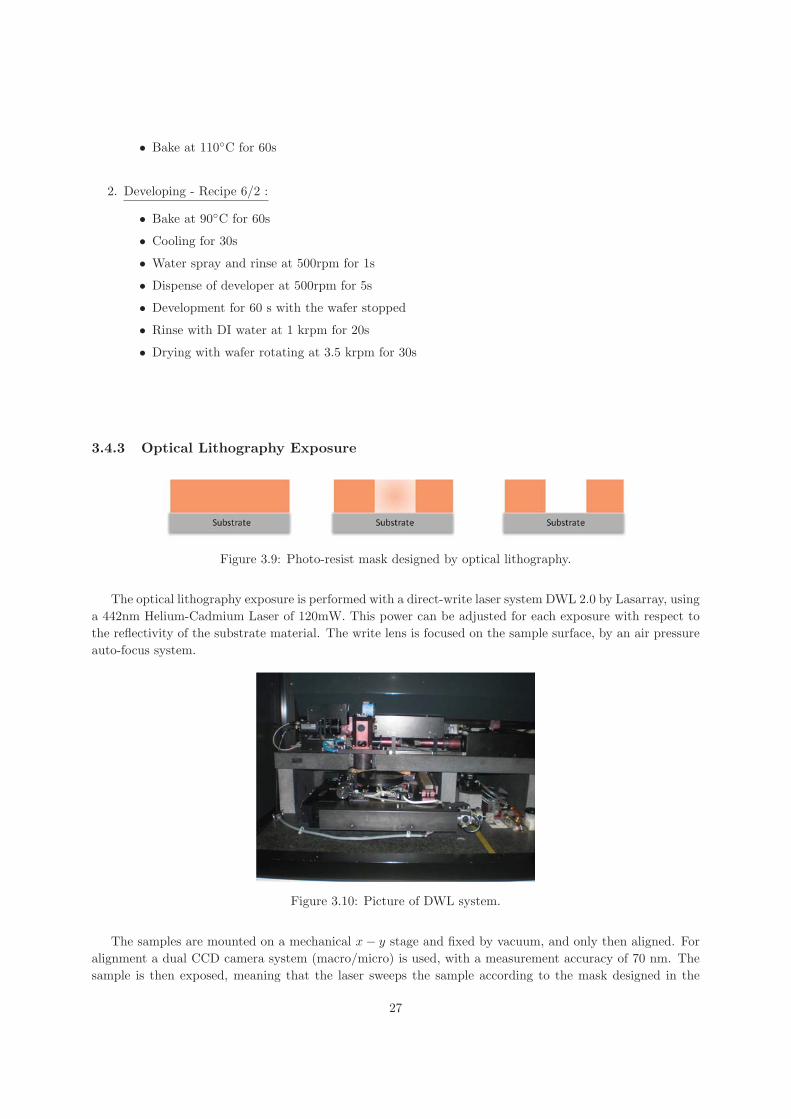
Figure 3.9: Photo-resist mask designed by optical lithography.
The optical lithography exposure is performed with a direct-write laser system DWL 2.0 by Lasarray, using
a 442nm Helium-Cadmium Laser of 120mW. This power can be adjusted for each exposure with respect to
the reflectivity of the substrate material. The write lens is focused on the sample surface, by an air pressure
auto-focus system.
Figure 3.10: Picture of DWL system.
The samples are mounted on a mechanical x− y stage and fixed by vacuum, and only then aligned. For
alignment a dual CCD camera system (macro/micro) is used, with a measurement accuracy of 70 nm. The
sample is then exposed, meaning that the laser sweeps the sample according to the mask designed in the
27
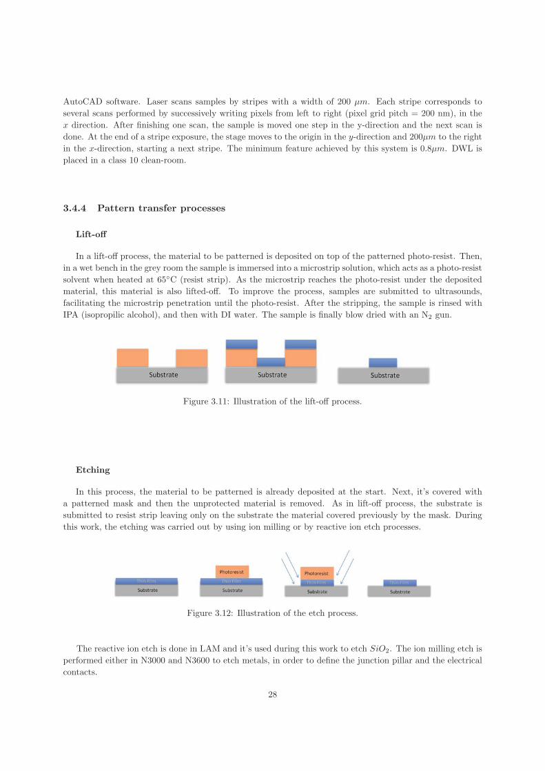
AutoCAD software. Laser scans samples by stripes with a width of 200 μm. Each stripe corresponds to
several scans performed by successively writing pixels from left to right (pixel grid pitch = 200 nm), in the
x direction. After finishing one scan, the sample is moved one step in the y-direction and the next scan is
done. At the end of a stripe exposure, the stage moves to the origin in the y-direction and 200μm to the right
in the x-direction, starting a next stripe. The minimum feature achieved by this system is 0.8μm. DWL is
placed in a class 10 clean-room.
3.4.4 Pattern transfer processes
Lift-off
In a lift-off process, the material to be patterned is deposited on top of the patterned photo-resist. Then,
in a wet bench in the grey room the sample is immersed into a microstrip solution, which acts as a photo-resist
solvent when heated at 65◦C (resist strip). As the microstrip reaches the photo-resist under the deposited
material, this material is also lifted-off. To improve the process, samples are submitted to ultrasounds,
facilitating the microstrip penetration until the photo-resist. After the stripping, the sample is rinsed with
IPA (isopropilic alcohol), and then with DI water. The sample is finally blow dried with an N2 gun.
Figure 3.11: Illustration of the lift-off process.
Etching
In this process, the material to be patterned is already deposited at the start. Next, it’s covered with
a patterned mask and then the unprotected material is removed. As in lift-off process, the substrate is
submitted to resist strip leaving only on the substrate the material covered previously by the mask. During
this work, the etching was carried out by using ion milling or by reactive ion etch processes.
Figure 3.12: Illustration of the etch process.
The reactive ion etch is done in LAM and it’s used during this work to etch SiO2. The ion milling etch is
performed either in N3000 and N3600 to etch metals, in order to define the junction pillar and the electrical
contacts.
28
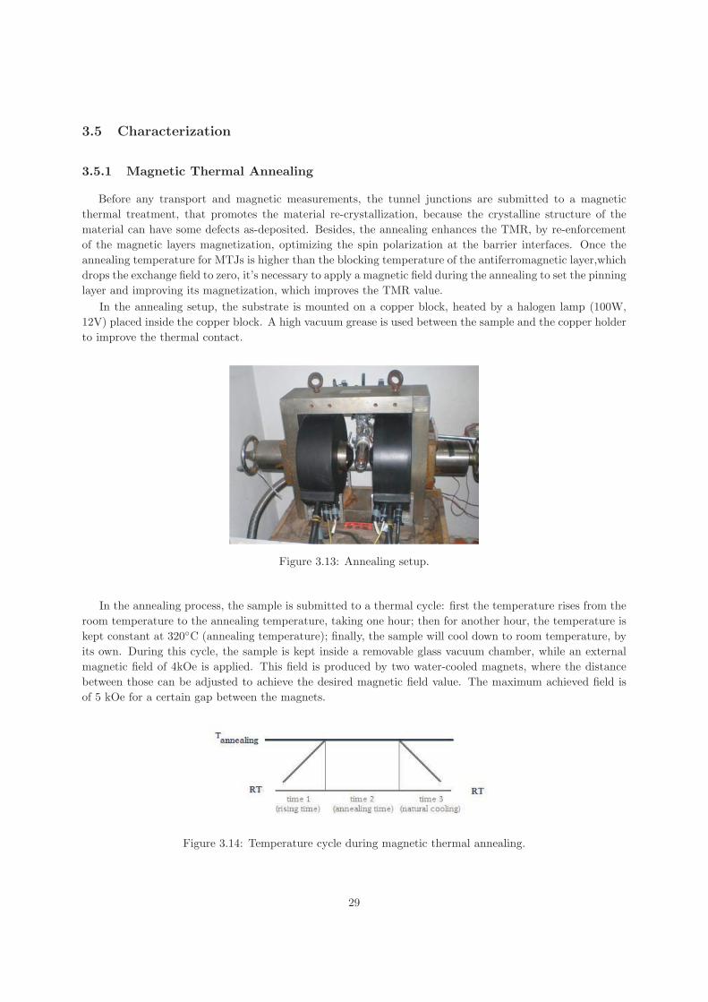
3.5 Characterization
3.5.1 Magnetic Thermal Annealing
Before any transport and magnetic measurements, the tunnel junctions are submitted to a magnetic
thermal treatment, that promotes the material re-crystallization, because the crystalline structure of the
material can have some defects as-deposited. Besides, the annealing enhances the TMR, by re-enforcement
of the magnetic layers magnetization, optimizing the spin polarization at the barrier interfaces. Once the
annealing temperature for MTJs is higher than the blocking temperature of the antiferromagnetic layer,which
drops the exchange field to zero, it’s necessary to apply a magnetic field during the annealing to set the pinning
layer and improving its magnetization, which improves the TMR value.
In the annealing setup, the substrate is mounted on a copper block, heated by a halogen lamp (100W,
12V) placed inside the copper block. A high vacuum grease is used between the sample and the copper holder
to improve the thermal contact.
Figure 3.13: Annealing setup.
In the annealing process, the sample is submitted to a thermal cycle: first the temperature rises from the
room temperature to the annealing temperature, taking one hour; then for another hour, the temperature is
kept constant at 320◦C (annealing temperature); finally, the sample will cool down to room temperature, by
its own. During this cycle, the sample is kept inside a removable glass vacuum chamber, while an external
magnetic field of 4kOe is applied. This field is produced by two water-cooled magnets, where the distance
between those can be adjusted to achieve the desired magnetic field value. The maximum achieved field is
of 5 kOe for a certain gap between the magnets.
Figure 3.14: Temperature cycle during magnetic thermal annealing.
29
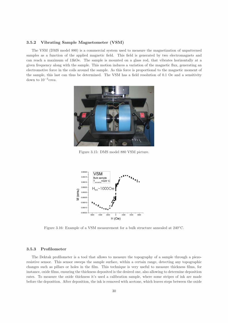
3.5.2 Vibrating Sample Magnetometer (VSM)
The VSM (DMS model 880) is a commercial system used to measure the magnetization of unpatterned
samples as a function of the applied magnetic field. This field is generated by two electromagnets and
can reach a maximum of 13kOe. The sample is mounted on a glass rod, that vibrates horizontally at a
given frequency along with the sample. This motion induces a variation of the magnetic flux, generating an
electromotive force in the coils around the sample. As this force is proportional to the magnetic moment of
the sample, this last can thus be determined. The VSM has a field resolution of 0.1 Oe and a sensitivity
down to 10−5emu.
Figure 3.15: DMS model 880 VSM picture.
Figure 3.16: Example of a VSM measurement for a bulk structure annealed at 240◦C.
3.5.3 Profilometer
The Dektak profilometer is a tool that allows to measure the topography of a sample through a piezo-
resistive sensor. This sensor sweeps the sample surface, within a certain range, detecting any topographic
changes such as pillars or holes in the film. This technique is very useful to measure thickness films, for
instance, oxide films, ensuring the thickness deposited is the desired one, also allowing to determine deposition
rates. To measure the oxide thickness it’s used a calibration sample, where some stripes of ink are made
before the deposition. After deposition, the ink is removed with acetone, which leaves steps between the oxide
30
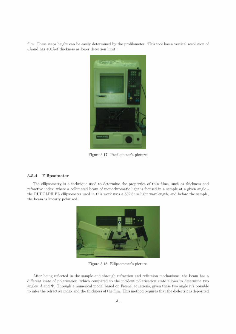
film. These steps height can be easily determined by the profilometer. This tool has a vertical resolution of
5Aand has 400Aof thickness as lower detection limit .
Figure 3.17: Profilometer’s picture.
3.5.4 Ellipsometer
The ellipsometry is a technique used to determine the properties of thin films, such as thickness and
refractive index, where a collimated beam of monochromatic light is focused in a sample at a given angle -
the RUDOLPH EL ellipsometer used in this work uses a 632.8nm light wavelength, and before the sample,
the beam is linearly polarized.
Figure 3.18: Ellipsometer’s picture.
After being reflected in the sample and through refraction and reflection mechanisms, the beam has a
different state of polarization, which compared to the incident polarization state allows to determine two
angles: δ and Ψ. Through a numerical model based on Fresnel equations, given these two angle it’s possible
to infer the refractive index and the thickness of the film. This method requires that the dielectric is deposited
31

on top of a fully reflective material, such as silicon, Si. As the profilometer, this method allows to calibrate
the thickness of the deposited oxide (Al2O3 and SiO2) but further, it also helps to ensure the oxide target is
not contaminated through the determination of the refractive index, which is well known for each material:
1.62 for Al2O3 and 1.47 for SiO2.
32
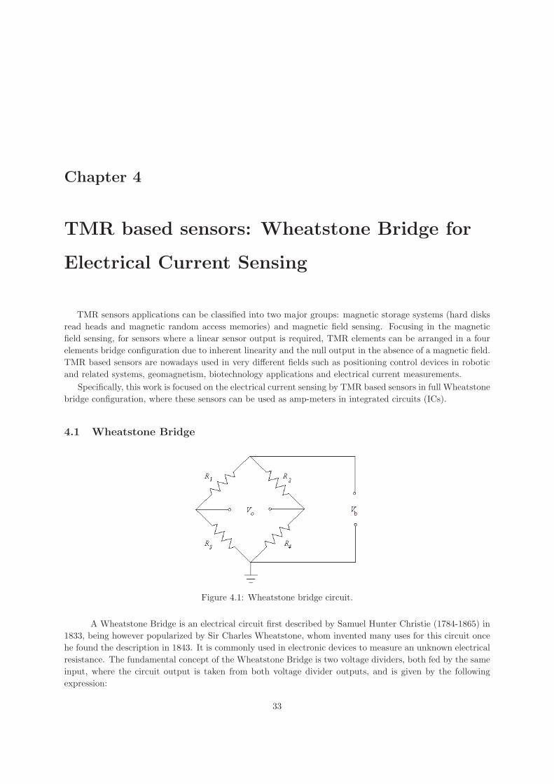
Chapter 4
TMR based sensors: Wheatstone Bridge for
Electrical Current Sensing
TMR sensors applications can be classified into two major groups: magnetic storage systems (hard disks
read heads and magnetic random access memories) and magnetic field sensing. Focusing in the magnetic
field sensing, for sensors where a linear sensor output is required, TMR elements can be arranged in a four
elements bridge configuration due to inherent linearity and the null output in the absence of a magnetic field.
TMR based sensors are nowadays used in very different fields such as positioning control devices in robotic
and related systems, geomagnetism, biotechnology applications and electrical current measurements.
Specifically, this work is focused on the electrical current sensing by TMR based sensors in full Wheatstone
bridge configuration, where these sensors can be used as amp-meters in integrated circuits (ICs).
4.1 Wheatstone Bridge
Figure 4.1: Wheatstone bridge circuit.
A Wheatstone Bridge is an electrical circuit first described by Samuel Hunter Christie (1784-1865) in
1833, being however popularized by Sir Charles Wheatstone, whom invented many uses for this circuit once
he found the description in 1843. It is commonly used in electronic devices to measure an unknown electrical
resistance. The fundamental concept of the Wheatstone Bridge is two voltage dividers, both fed by the same
input, where the circuit output is taken from both voltage divider outputs, and is given by the following
expression:
33

Vo =
(R2
R1 +R2− R4
R3 +R4
)Vi (4.1)
In its classic form, a galvanometer (a very sensitive dc current meter) is connected between the output
terminals, and is used to monitor the current flowing from one voltage divider to the other. If the two voltage
dividers have exactly the same ratio R1/R3 = R2/R4, then the bridge is said to be balanced and no current
flows in either direction through the galvanometer, being the output null. If one of the resistors changes even
a little bit in value, the bridge will become unbalanced and current will flow through the galvanometer.
Even though a unique resistance can be used as sensing element, a Wheatstone bridge setup is always a
good recommendation as the starting step in the design of resistive sensors, since it provides a differential
output as a function of the resistance variation. In fact, using MTJs as resist elements in a Wheatstone
Bridge allows to have a linear magnetic field sensor with an offset-free signal.
Depending on the considered case or the particular requirements, there are several bridge configurations
that can be used [20], [21], [22].
4.1.1 Quarter Bridge Configuration
In this configuration, four resistances of identical nominal value are used, being only one of them active:
R1 = R2 = R3 = R and R4 = R+ΔR. In this case, the output voltage is given by:
Vo =ΔRR
2(2 + ΔR
R
)Vb (4.2)
The relationship of the bridge output with the variation of resistance is not linear. Besides, to obtain a
output value of the order of the ΔRR ratio, a high Vb is required. This configuration is only used when small
variations of ΔR occur.
4.1.2 Half Bridge Configuration
In the half bridge configuration, two opposite resistances in the bridge are active: R2 = R3 = R and
R1 = R4 = R+ΔR. The output voltage is:
Vo =ΔRR
2 + ΔRR
Vb (4.3)
As in the previous configuration the output is non-linear, although the output value is now the double of
the previous.
4.1.3 Full Bridge Configuration
In order to get a full bridge response, paired resistances need to be made active: R1 = R4 = R+ΔR and
R2 = R3 = R−ΔR, and the output is given by:
Vo =ΔR
RVb (4.4)
This configurations shows to be the preferable one, since the output is linear and it has the higher output
signal, when compared to previous configurations.
34
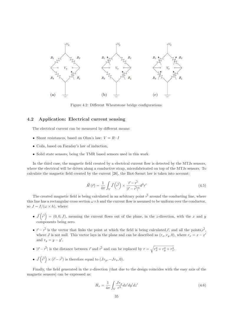
Figure 4.2: Different Wheatstone bridge configurations.
4.2 Application: Electrical current sensing
The electrical current can be measured by different means:
• Shunt resistances, based on Ohm’s law: V = R · I• Coils, based on Faraday’s law of induction,
• Solid state sensors, being the TMR based sensors used in this work.
In the third case, the magnetic field created by a electrical current flow is detected by the MTJs sensors,
where the electrical will be driven along a conductive strap, microfabricated on top of the MTJs sensors. To
calculate the magnetic field created by the current [26], the Biot-Savart law is taken into account:
H (r) =1
4π
∫V
J(r′)× r − r′
|r − r′|3 d3r′ (4.5)
The created magnetic field is being calculated in an arbitrary point r′ around the conducting line, where
this line has a rectangular cross section ω×h and the current flow is assumed to be uniform over the conductor,
so J = I/(ω × h), where:
• J(r′)
= (0, 0, J), meaning the current flows out of the plane, in the z-direction, with the x and y
components being zero.
• r − r′ is the vector that links the point at which the field is being calculated,r, and all the points,r′,where J is not null. This vector lays in the plane and can be described as (rx, ry, 0), where rx = x− x′
and ry = y − y′.
• |r − r′| is the distance between r and r′ and can be replaced by r =√
r2x + r2y + r2z .
• J(r′)× (r − r′) is therefore equal to (Jry,−Jrx, 0).
Finally, the field generated in the x-direction (that due to the design coincides with the easy axis of the
magnetic sensors) can be expressed as:
Hx =1
4π
∫V
Jryr3
dx′dy′dz′ (4.6)
35
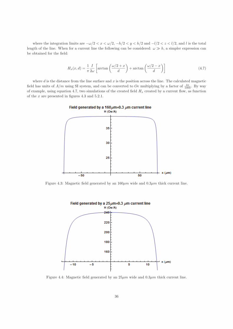
where the integration limits are −ω/2 < x < ω/2, −h/2 < y < h/2 and −l/2 < z < l/2, and l is the total
length of the line. When for a current line the following can be considered: ω h, a simpler expression can
be obtained for the field:
Hx(x, d) =1
π
I
2ω
[arctan
(ω/2 + x
d
)+ arctan
(ω/2− x
d
)](4.7)
where d is the distance from the line surface and x is the position across the line. The calculated magnetic
field has units of A/m using SI system, and can be converted to Oe multiplying by a factor of 4π1000 . By way
of example, using equation 4.7, two simulations of the created field Hx created by a current flow, as function
of the x are presented in figures 4.3 and 5.2.1.
Figure 4.3: Magnetic field generated by an 160μm wide and 0.3μm thick current line.
Figure 4.4: Magnetic field generated by an 25μm wide and 0.3μm thick current line.
36
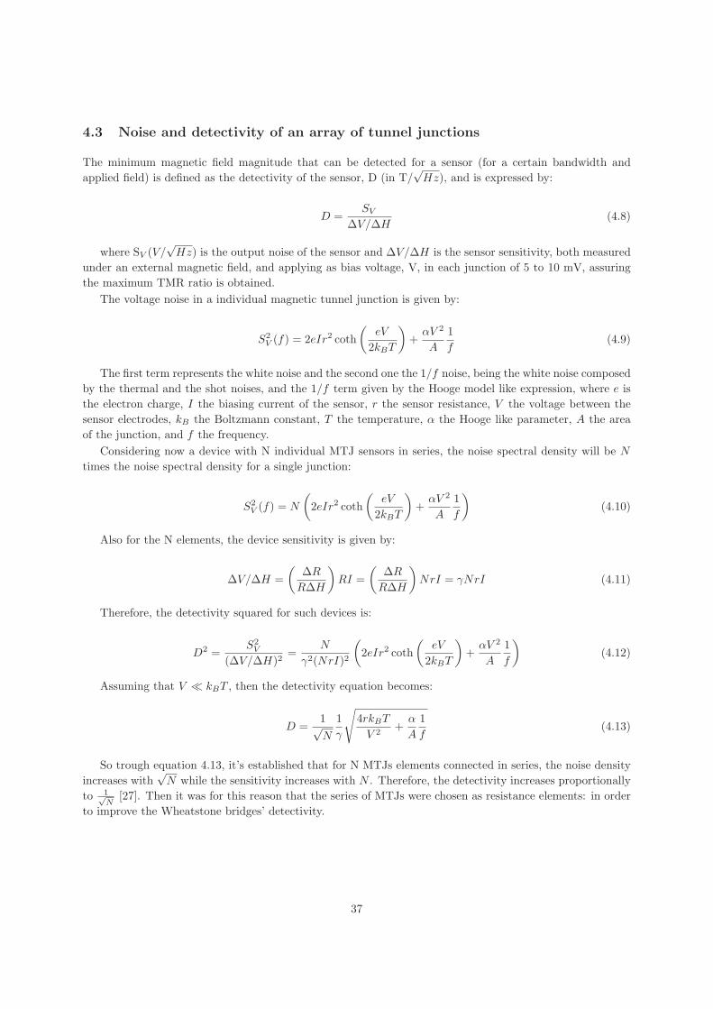
4.3 Noise and detectivity of an array of tunnel junctions
The minimum magnetic field magnitude that can be detected for a sensor (for a certain bandwidth and
applied field) is defined as the detectivity of the sensor, D (in T/√Hz), and is expressed by:
D =SV
ΔV/ΔH(4.8)
where SV (V/√Hz) is the output noise of the sensor and ΔV/ΔH is the sensor sensitivity, both measured
under an external magnetic field, and applying as bias voltage, V, in each junction of 5 to 10 mV, assuring
the maximum TMR ratio is obtained.
The voltage noise in a individual magnetic tunnel junction is given by:
S2V (f) = 2eIr2 coth
(eV
2kBT
)+
αV 2
A
1
f(4.9)
The first term represents the white noise and the second one the 1/f noise, being the white noise composed
by the thermal and the shot noises, and the 1/f term given by the Hooge model like expression, where e is
the electron charge, I the biasing current of the sensor, r the sensor resistance, V the voltage between the
sensor electrodes, kB the Boltzmann constant, T the temperature, α the Hooge like parameter, A the area
of the junction, and f the frequency.
Considering now a device with N individual MTJ sensors in series, the noise spectral density will be N
times the noise spectral density for a single junction:
S2V (f) = N
(2eIr2 coth
(eV
2kBT
)+
αV 2
A
1
f
)(4.10)
Also for the N elements, the device sensitivity is given by:
ΔV/ΔH =
(ΔR
RΔH
)RI =
(ΔR
RΔH
)NrI = γNrI (4.11)
Therefore, the detectivity squared for such devices is:
D2 =S2V
(ΔV/ΔH)2=
N
γ2(NrI)2
(2eIr2 coth
(eV
2kBT
)+
αV 2
A
1
f
)(4.12)
Assuming that V � kBT , then the detectivity equation becomes:
D =1√N
1
γ
√4rkBT
V 2+
α
A
1
f(4.13)
So trough equation 4.13, it’s established that for N MTJs elements connected in series, the noise density
increases with√N while the sensitivity increases with N . Therefore, the detectivity increases proportionally
to 1√N
[27]. Then it was for this reason that the series of MTJs were chosen as resistance elements: in order
to improve the Wheatstone bridges’ detectivity.
37
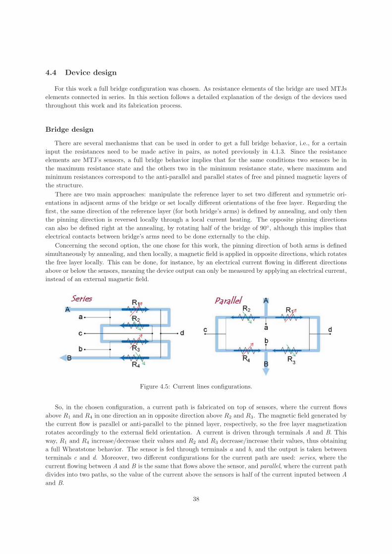
4.4 Device design
For this work a full bridge configuration was chosen. As resistance elements of the bridge are used MTJs
elements connected in series. In this section follows a detailed explanation of the design of the devices used
throughout this work and its fabrication process.
Bridge design
There are several mechanisms that can be used in order to get a full bridge behavior, i.e., for a certain
input the resistances need to be made active in pairs, as noted previously in 4.1.3. Since the resistance
elements are MTJ’s sensors, a full bridge behavior implies that for the same conditions two sensors be in
the maximum resistance state and the others two in the minimum resistance state, where maximum and
minimum resistances correspond to the anti-parallel and parallel states of free and pinned magnetic layers of
the structure.
There are two main approaches: manipulate the reference layer to set two different and symmetric ori-
entations in adjacent arms of the bridge or set locally different orientations of the free layer. Regarding the
first, the same direction of the reference layer (for both bridge’s arms) is defined by annealing, and only then
the pinning direction is reversed locally through a local current heating. The opposite pinning directions
can also be defined right at the annealing, by rotating half of the bridge of 90◦, although this implies that
electrical contacts between bridge’s arms need to be done externally to the chip.
Concerning the second option, the one chose for this work, the pinning direction of both arms is defined
simultaneously by annealing, and then locally, a magnetic field is applied in opposite directions, which rotates
the free layer locally. This can be done, for instance, by an electrical current flowing in different directions
above or below the sensors, meaning the device output can only be measured by applying an electrical current,
instead of an external magnetic field.
Figure 4.5: Current lines configurations.
So, in the chosen configuration, a current path is fabricated on top of sensors, where the current flows
above R1 and R4 in one direction an in opposite direction above R2 and R3. The magnetic field generated by
the current flow is parallel or anti-parallel to the pinned layer, respectively, so the free layer magnetization
rotates accordingly to the external field orientation. A current is driven through terminals A and B. This
way, R1 and R4 increase/decrease their values and R2 and R3 decrease/increase their values, thus obtaining
a full Wheatstone behavior. The sensor is fed through terminals a and b, and the output is taken between
terminals c and d. Moreover, two different configurations for the current path are used: series, where the
current flowing between A and B is the same that flows above the sensor, and parallel, where the current path
divides into two paths, so the value of the current above the sensors is half of the current inputed between A
and B.
38
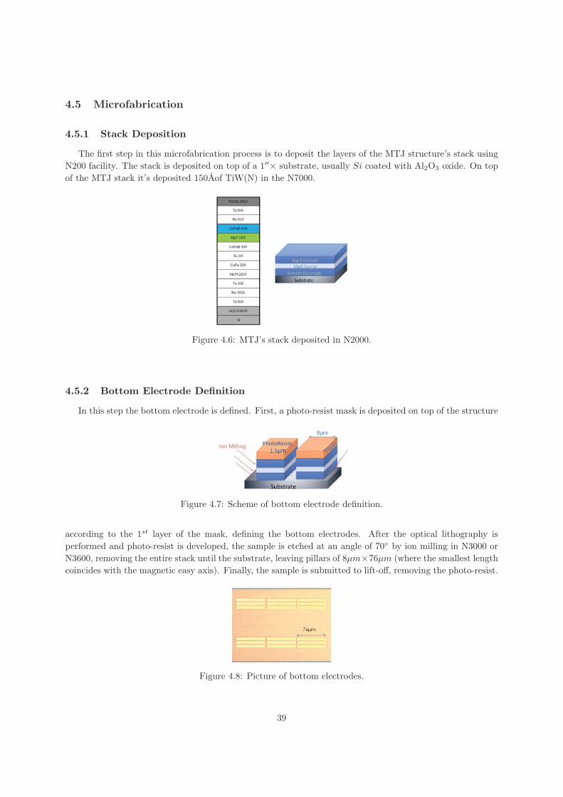
4.5 Microfabrication
4.5.1 Stack Deposition
The first step in this microfabrication process is to deposit the layers of the MTJ structure’s stack using
N200 facility. The stack is deposited on top of a 1′′× substrate, usually Si coated with Al2O3 oxide. On top
of the MTJ stack it’s deposited 150Aof TiW(N) in the N7000.
Figure 4.6: MTJ’s stack deposited in N2000.
4.5.2 Bottom Electrode Definition
In this step the bottom electrode is defined. First, a photo-resist mask is deposited on top of the structure
Figure 4.7: Scheme of bottom electrode definition.
according to the 1st layer of the mask, defining the bottom electrodes. After the optical lithography is
performed and photo-resist is developed, the sample is etched at an angle of 70◦ by ion milling in N3000 or
N3600, removing the entire stack until the substrate, leaving pillars of 8μm×76μm (where the smallest length
coincides with the magnetic easy axis). Finally, the sample is submitted to lift-off, removing the photo-resist.
Figure 4.8: Picture of bottom electrodes.
39
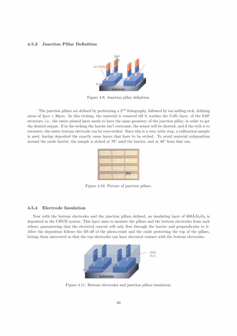
4.5.3 Junction Pillar Definition
Figure 4.9: Junction pillar definition.
The junction pillars are defined by performing a 2nd lithography, followed by ion milling etch, defining
areas of 2μm × 30μm. In this etching, the material is removed till it reaches the CoFe layer, of the SAF
structure, i.e., the entire pinned layer needs to have the same geometry of the junction pillar, in order to get
the desired output. If in the etching the barrier isn’t overcame, the sensor will be shorted, and if the etch is to
excessive, the entire bottom electrode can be over-etched. Since this is a very critic step, a calibration sample
is used, having deposited the exactly same layers that have to be etched. To avoid material redeposition
around the oxide barrier, the sample is etched at 70◦ until the barrier, and at 40◦ from that one.
Figure 4.10: Picture of junction pillars.
4.5.4 Electrode Insulation
Now with the bottom electrodes and the junction pillars defined, an insulating layer of 800AAl2O3 is
deposited in the UHVII system. This layer aims to insulate the pillars and the bottom electrodes from each
others, guaranteeing that the electrical current will only flow through the barrier and perpendicular to it.
After the deposition follows the lift-off of the photo-resist and the oxide protecting the top of the pillars,
letting them uncovered so that the top electrodes can have electrical contact with the bottom electrodes.
Figure 4.11: Bottom electrodes and junction pillars insulation.
40
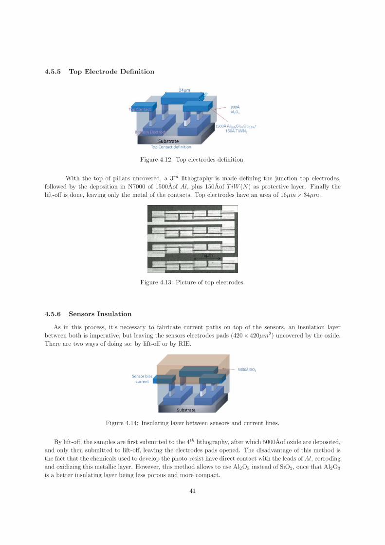
4.5.5 Top Electrode Definition
Figure 4.12: Top electrodes definition.
With the top of pillars uncovered, a 3rd lithography is made defining the junction top electrodes,
followed by the deposition in N7000 of 1500Aof Al, plus 150Aof T iW (N) as protective layer. Finally the
lift-off is done, leaving only the metal of the contacts. Top electrodes have an area of 16μm× 34μm.
Figure 4.13: Picture of top electrodes.
4.5.6 Sensors Insulation
As in this process, it’s necessary to fabricate current paths on top of the sensors, an insulation layer
between both is imperative, but leaving the sensors electrodes pads (420× 420μm2) uncovered by the oxide.
There are two ways of doing so: by lift-off or by RIE.
Figure 4.14: Insulating layer between sensors and current lines.
By lift-off, the samples are first submitted to the 4th lithography, after which 5000Aof oxide are deposited,
and only then submitted to lift-off, leaving the electrodes pads opened. The disadvantage of this method is
the fact that the chemicals used to develop the photo-resist have direct contact with the leads of Al, corroding
and oxidizing this metallic layer. However, this method allows to use Al2O3 instead of SiO2, once that Al2O3
is a better insulating layer being less porous and more compact.
41
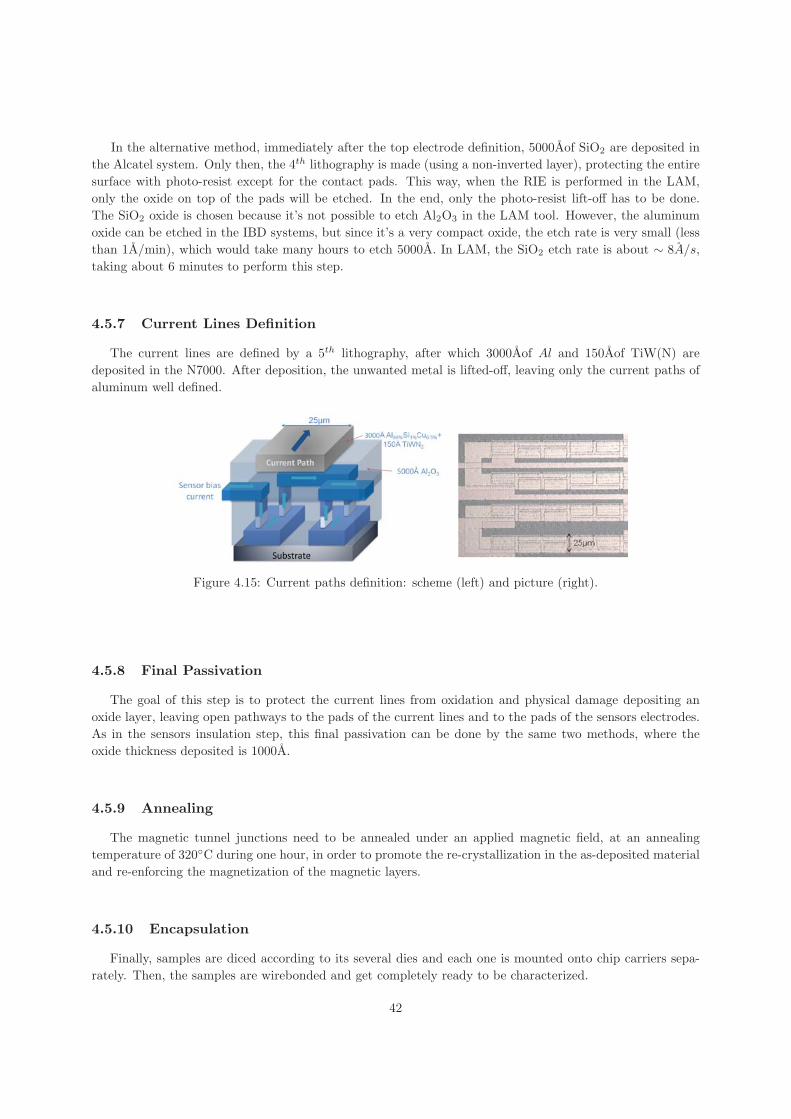
In the alternative method, immediately after the top electrode definition, 5000Aof SiO2 are deposited in
the Alcatel system. Only then, the 4th lithography is made (using a non-inverted layer), protecting the entire
surface with photo-resist except for the contact pads. This way, when the RIE is performed in the LAM,
only the oxide on top of the pads will be etched. In the end, only the photo-resist lift-off has to be done.
The SiO2 oxide is chosen because it’s not possible to etch Al2O3 in the LAM tool. However, the aluminum
oxide can be etched in the IBD systems, but since it’s a very compact oxide, the etch rate is very small (less
than 1A/min), which would take many hours to etch 5000A. In LAM, the SiO2 etch rate is about ∼ 8A/s,
taking about 6 minutes to perform this step.
4.5.7 Current Lines Definition
The current lines are defined by a 5th lithography, after which 3000Aof Al and 150Aof TiW(N) are
deposited in the N7000. After deposition, the unwanted metal is lifted-off, leaving only the current paths of
aluminum well defined.
Figure 4.15: Current paths definition: scheme (left) and picture (right).
4.5.8 Final Passivation
The goal of this step is to protect the current lines from oxidation and physical damage depositing an
oxide layer, leaving open pathways to the pads of the current lines and to the pads of the sensors electrodes.
As in the sensors insulation step, this final passivation can be done by the same two methods, where the
oxide thickness deposited is 1000A.
4.5.9 Annealing
The magnetic tunnel junctions need to be annealed under an applied magnetic field, at an annealing
temperature of 320◦C during one hour, in order to promote the re-crystallization in the as-deposited material
and re-enforcing the magnetization of the magnetic layers.
4.5.10 Encapsulation
Finally, samples are diced according to its several dies and each one is mounted onto chip carriers sepa-
rately. Then, the samples are wirebonded and get completely ready to be characterized.
42
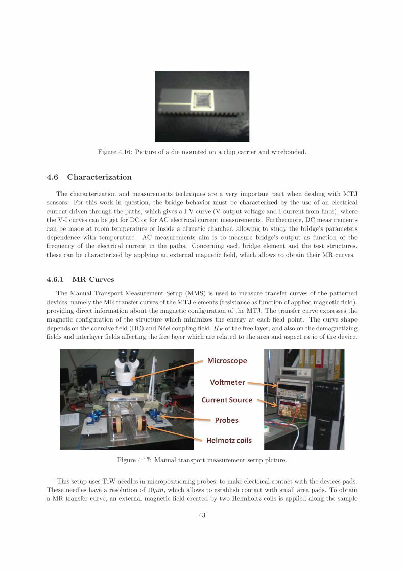
Figure 4.16: Picture of a die mounted on a chip carrier and wirebonded.
4.6 Characterization
The characterization and measurements techniques are a very important part when dealing with MTJ
sensors. For this work in question, the bridge behavior must be characterized by the use of an electrical
current driven through the paths, which gives a I-V curve (V-output voltage and I-current from lines), where
the V-I curves can be get for DC or for AC electrical current measurements. Furthermore, DC measurements
can be made at room temperature or inside a climatic chamber, allowing to study the bridge’s parameters
dependence with temperature. AC measurements aim is to measure bridge’s output as function of the
frequency of the electrical current in the paths. Concerning each bridge element and the test structures,
these can be characterized by applying an external magnetic field, which allows to obtain their MR curves.
4.6.1 MR Curves
The Manual Transport Measurement Setup (MMS) is used to measure transfer curves of the patterned
devices, namely the MR transfer curves of the MTJ elements (resistance as function of applied magnetic field),
providing direct information about the magnetic configuration of the MTJ. The transfer curve expresses the
magnetic configuration of the structure which minimizes the energy at each field point. The curve shape
depends on the coercive field (HC) and Neel coupling field, HF of the free layer, and also on the demagnetizing
fields and interlayer fields affecting the free layer which are related to the area and aspect ratio of the device.
Figure 4.17: Manual transport measurement setup picture.
This setup uses TiW needles in micropositioning probes, to make electrical contact with the devices pads.
These needles have a resolution of 10μm, which allows to establish contact with small area pads. To obtain
a MR transfer curve, an external magnetic field created by two Helmholtz coils is applied along the sample
43
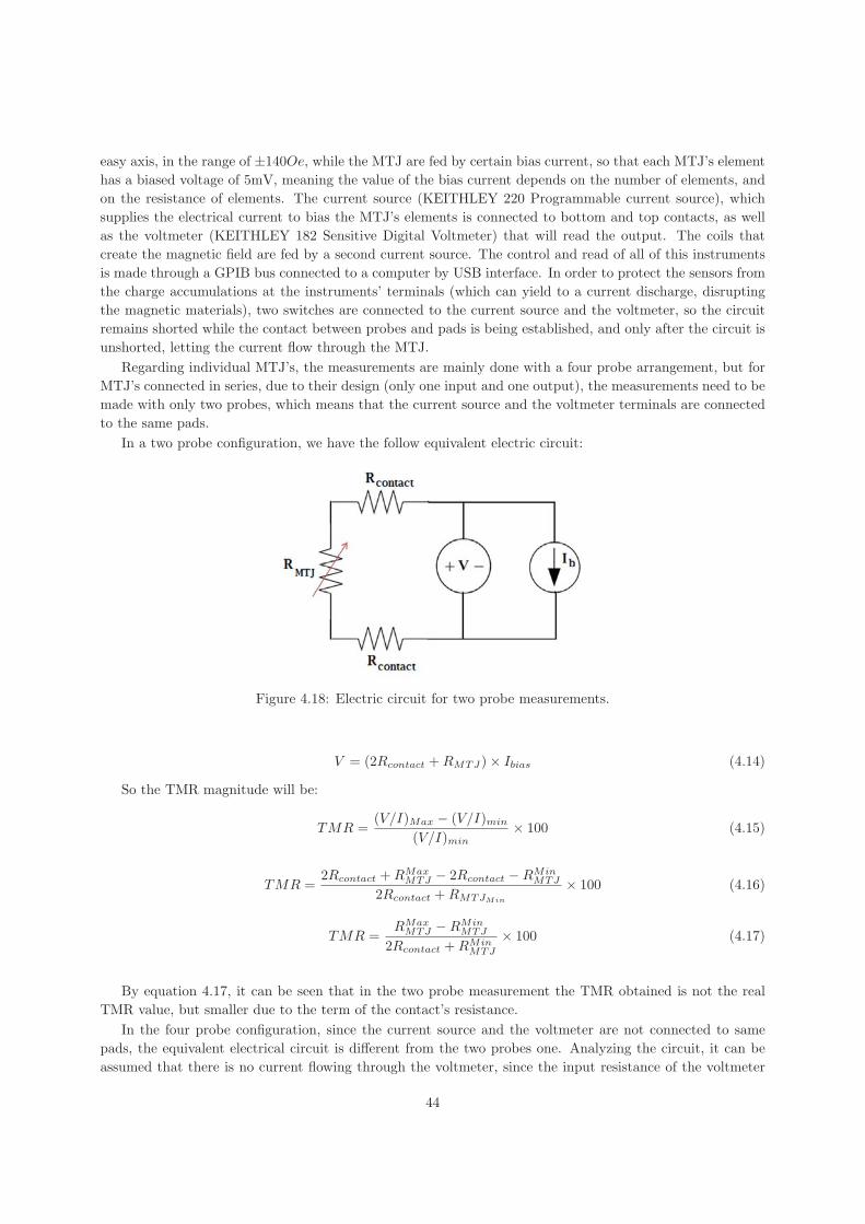
easy axis, in the range of ±140Oe, while the MTJ are fed by certain bias current, so that each MTJ’s element
has a biased voltage of 5mV, meaning the value of the bias current depends on the number of elements, and
on the resistance of elements. The current source (KEITHLEY 220 Programmable current source), which
supplies the electrical current to bias the MTJ’s elements is connected to bottom and top contacts, as well
as the voltmeter (KEITHLEY 182 Sensitive Digital Voltmeter) that will read the output. The coils that
create the magnetic field are fed by a second current source. The control and read of all of this instruments
is made through a GPIB bus connected to a computer by USB interface. In order to protect the sensors from
the charge accumulations at the instruments’ terminals (which can yield to a current discharge, disrupting
the magnetic materials), two switches are connected to the current source and the voltmeter, so the circuit
remains shorted while the contact between probes and pads is being established, and only after the circuit is
unshorted, letting the current flow through the MTJ.
Regarding individual MTJ’s, the measurements are mainly done with a four probe arrangement, but for
MTJ’s connected in series, due to their design (only one input and one output), the measurements need to be
made with only two probes, which means that the current source and the voltmeter terminals are connected
to the same pads.
In a two probe configuration, we have the follow equivalent electric circuit:
Figure 4.18: Electric circuit for two probe measurements.
V = (2Rcontact +RMTJ)× Ibias (4.14)
So the TMR magnitude will be:
TMR =(V/I)Max − (V/I)min
(V/I)min× 100 (4.15)
TMR =2Rcontact +RMax
MTJ − 2Rcontact −RMinMTJ
2Rcontact +RMTJMin
× 100 (4.16)
TMR =RMax
MTJ −RMinMTJ
2Rcontact +RMinMTJ
× 100 (4.17)
By equation 4.17, it can be seen that in the two probe measurement the TMR obtained is not the real
TMR value, but smaller due to the term of the contact’s resistance.
In the four probe configuration, since the current source and the voltmeter are not connected to same
pads, the equivalent electrical circuit is different from the two probes one. Analyzing the circuit, it can be
assumed that there is no current flowing through the voltmeter, since the input resistance of the voltmeter
44
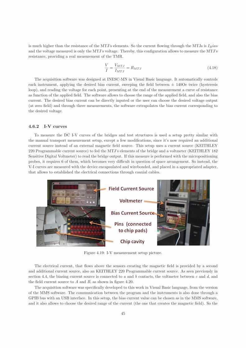
is much higher than the resistance of the MTJ’s elements. So the current flowing through the MTJs is IBias
and the voltage measured is only the MTJ’s voltage. Thereby, this configuration allows to measure the MTJ’s
resistance, providing a real measurement of the TMR.
V
I=
VMTJ
IMTJ= RMTJ (4.18)
The acquisition software was designed at INESC-MN in Visual Basic language. It automatically controls
each instrument, applying the desired bias current, sweeping the field between ± 140Oe twice (hysteresis
loop), and reading the voltage for each point, presenting at the end of the measurement a curve of resistance
as function of the applied field. The software allows to choose the range of the applied field, and also the bias
current. The desired bias current can be directly inputed or the user can choose the desired voltage output
(at zero field) and through three measurements, the software extrapolates the bias current corresponding to
the desired voltage.
4.6.2 I-V curves
To measure the DC I-V curves of the bridges and test structures is used a setup pretty similar with
the manual transport measurement setup, except a few modifications, since it’s now required an additional
current source instead of an external magnetic field source. This setup uses a current source (KEITHLEY
220 Programmable current source) to fed the MTJ’s elements of the bridge and a voltmeter (KEITHLEY 182
Sensitive Digital Voltmeter) to read the bridge output. If this measure is performed with the micropositioning
probes, it requires 6 of them, which becomes very difficult in question of space arrangement. So instead, the
V-I curves are measured with the device encapsulated and wirebonded, and placed in a appropriated adapter,
that allows to established the electrical connections through coaxial cables.
Figure 4.19: I-V measurement setup picture.
The electrical current, that flows above the sensors creating the magnetic field is provided by a second
and additional current source, also an KEITHLEY 220 Programmable current source. As seen previously in
section 4.4, the biasing current source is connected to a and b contacts, the voltmeter between c and d, and
the field current source to A and B, as shown in figure 4.20.
The acquisition software was specifically developed to this work in Visual Basic language, from the version
of the MMS software. The communication between the program and the instruments is also done through a
GPIB bus with an USB interface. In this setup, the bias current value can be chosen as in the MMS software,
and it also allows to choose the desired range of the current (the one that creates the magnetic field). So the
45
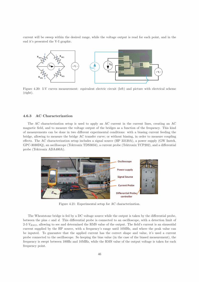
current will be sweep within the desired range, while the voltage output is read for each point, and in the
end it’s presented the V-I graphic.
Figure 4.20: I-V curves measurement: equivalent electric circuit (left) and picture with electrical scheme(right).
4.6.3 AC Characterization
The AC characterization setup is used to apply an AC current in the current lines, creating an AC
magnetic field, and to measure the voltage output of the bridges as a function of the frequency. This kind
of measurements can be done in two different experimental conditions: with a biasing current feeding the
bridge, allowing to measure the bridge AC transfer curve; or without biasing, in order to measure coupling
effects. The AC characterization setup includes a signal source (HP 33120A), a power supply (GW Instek,
GPC-3030DQ), an oscilloscope (Tektronix TDS3034), a current probe (Tektronix TCP202), and a differential
probe (Tektronix ADA400A).
Figure 4.21: Experimental setup for AC characterization.
The Wheatstone bridge is fed by a DC voltage source while the output is taken by the differential probe,
between the pins c and d. This differential probe is connected to an oscilloscope, with a detection limit of
2-3 VRMS , allowing to see and determined the RMS value of the output. The field’s current is an sinusoidal
current supplied by the HP source, with a frequency’s range until 10MHz, and where the peak value can
be inputed. To guarantee that the applied current has the correct shape and value, it’s used a current
probe connected to the oscilloscope. So keeping the bias value (in the case of the biased measurement), the
frequency is swept between 100Hz and 10MHz, while the RMS value of the output voltage is taken for each
frequency point.
46
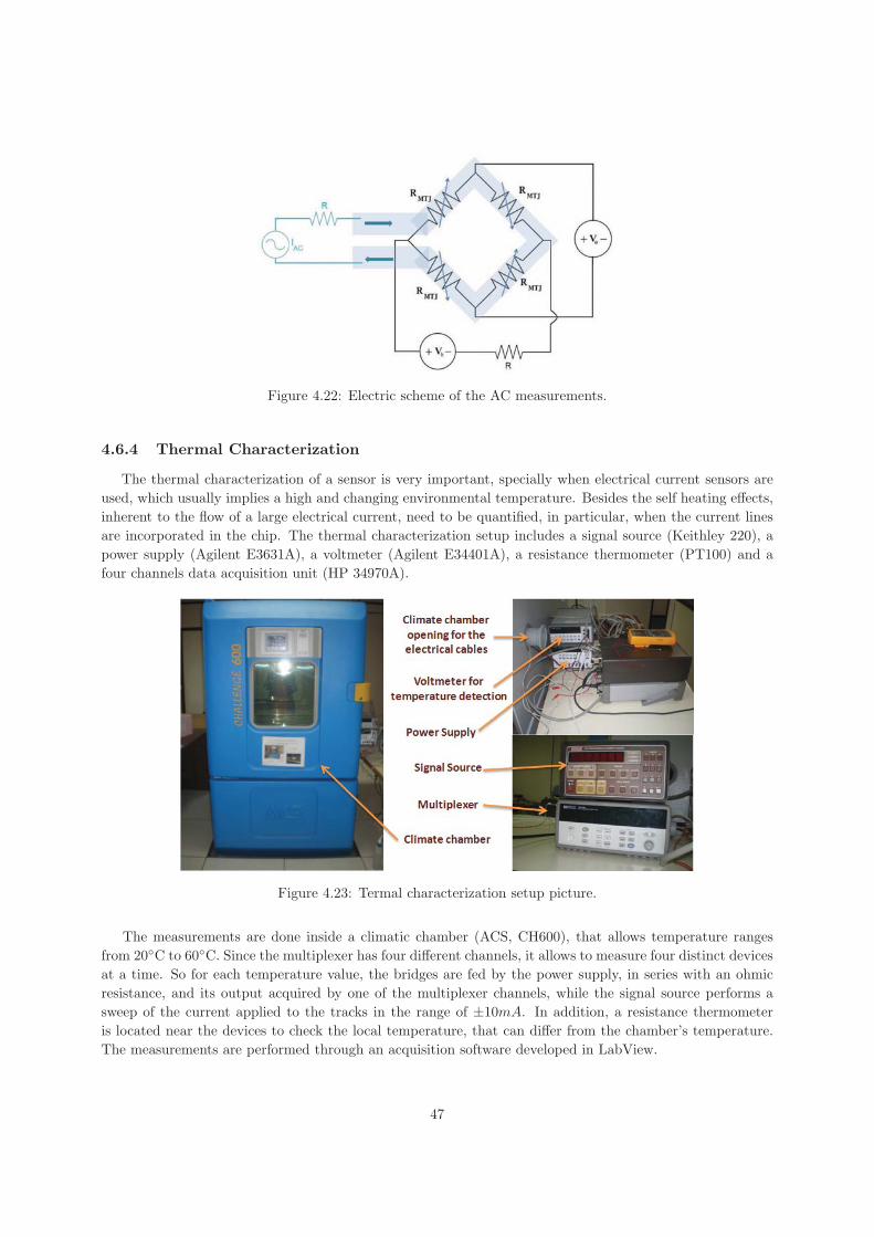
Figure 4.22: Electric scheme of the AC measurements.
4.6.4 Thermal Characterization
The thermal characterization of a sensor is very important, specially when electrical current sensors are
used, which usually implies a high and changing environmental temperature. Besides the self heating effects,
inherent to the flow of a large electrical current, need to be quantified, in particular, when the current lines
are incorporated in the chip. The thermal characterization setup includes a signal source (Keithley 220), a
power supply (Agilent E3631A), a voltmeter (Agilent E34401A), a resistance thermometer (PT100) and a
four channels data acquisition unit (HP 34970A).
Figure 4.23: Termal characterization setup picture.
The measurements are done inside a climatic chamber (ACS, CH600), that allows temperature ranges
from 20◦C to 60◦C. Since the multiplexer has four different channels, it allows to measure four distinct devices
at a time. So for each temperature value, the bridges are fed by the power supply, in series with an ohmic
resistance, and its output acquired by one of the multiplexer channels, while the signal source performs a
sweep of the current applied to the tracks in the range of ±10mA. In addition, a resistance thermometer
is located near the devices to check the local temperature, that can differ from the chamber’s temperature.
The measurements are performed through an acquisition software developed in LabView.
47

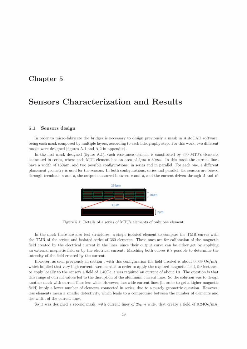
Chapter 5
Sensors Characterization and Results
5.1 Sensors design
In order to micro-fabricate the bridges is necessary to design previously a mask in AutoCAD software,
being each mask composed by multiple layers, according to each lithography step. For this work, two different
masks were designed [figures A.1 and A.2 in appendix] .
In the first mask designed (figure A.1), each resistance element is constituted by 390 MTJ’s elements
connected in series, where each MTJ element has an area of 2μm × 30μm. In this mask the current lines
have a width of 160μm, and two possible configurations: in series and in parallel. For each one, a different
placement geometry is used for the sensors. In both configurations, series and parallel, the sensors are biased
through terminals a and b, the output measured between c and d, and the current driven through A and B.
Figure 5.1: Details of a series of MTJ’s elements of only one element.
In the mask there are also test structures: a single isolated element to compare the TMR curves with
the TMR of the series; and isolated series of 360 elements. These ones are for calibration of the magnetic
field created by the electrical current in the lines, since their output curve can be either get by applying
an external magnetic field or by the electrical current. Matching both curves it’s possible to determine the
intensity of the field created by the current.
However, as seen previously in section , with this configuration the field created is about 0.039 Oe/mA,
which implied that very high currents were needed in order to apply the required magnetic field, for instance,
to apply locally to the sensors a field of ±40Oe it was required an current of about 1A. The question is that
this range of current values led to the disruption of the aluminum current lines. So the solution was to design
another mask with current lines less wide. However, less wide current lines (in order to get a higher magnetic
field) imply a lower number of elements connected in series, due to a purely geometric question. However,
less elements mean a smaller detectivity, which leads to a compromise between the number of elements and
the width of the current lines.
So it was designed a second mask, with current lines of 25μm wide, that create a field of 0.24Oe/mA.
49
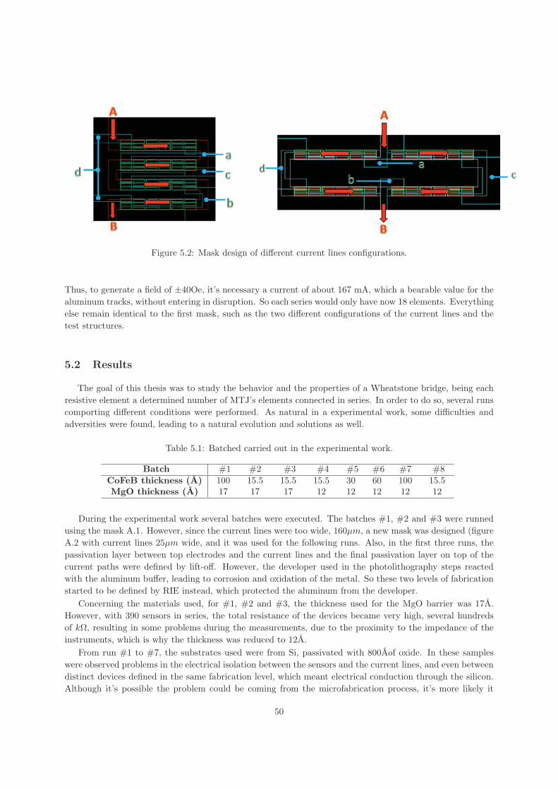
Figure 5.2: Mask design of different current lines configurations.
Thus, to generate a field of ±40Oe, it’s necessary a current of about 167 mA, which a bearable value for the
aluminum tracks, without entering in disruption. So each series would only have now 18 elements. Everything
else remain identical to the first mask, such as the two different configurations of the current lines and the
test structures.
5.2 Results
The goal of this thesis was to study the behavior and the properties of a Wheatstone bridge, being each
resistive element a determined number of MTJ’s elements connected in series. In order to do so, several runs
comporting different conditions were performed. As natural in a experimental work, some difficulties and
adversities were found, leading to a natural evolution and solutions as well.
Table 5.1: Batched carried out in the experimental work.
Batch #1 #2 #3 #4 #5 #6 #7 #8
CoFeB thickness (A) 100 15.5 15.5 15.5 30 60 100 15.5MgO thickness (A) 17 17 17 12 12 12 12 12
During the experimental work several batches were executed. The batches #1, #2 and #3 were runned
using the mask A.1. However, since the current lines were too wide, 160μm, a new mask was designed (figure
A.2 with current lines 25μm wide, and it was used for the following runs. Also, in the first three runs, the
passivation layer between top electrodes and the current lines and the final passivation layer on top of the
current paths were defined by lift-off. However, the developer used in the photolithography steps reacted
with the aluminum buffer, leading to corrosion and oxidation of the metal. So these two levels of fabrication
started to be defined by RIE instead, which protected the aluminum from the developer.
Concerning the materials used, for #1, #2 and #3, the thickness used for the MgO barrier was 17A.
However, with 390 sensors in series, the total resistance of the devices became very high, several hundreds
of kΩ, resulting in some problems during the measurements, due to the proximity to the impedance of the
instruments, which is why the thickness was reduced to 12A.
From run #1 to #7, the substrates used were from Si, passivated with 800Aof oxide. In these samples
were observed problems in the electrical isolation between the sensors and the current lines, and even between
distinct devices defined in the same fabrication level, which meant electrical conduction through the silicon.
Although it’s possible the problem could be coming from the microfabrication process, it’s more likely it
50
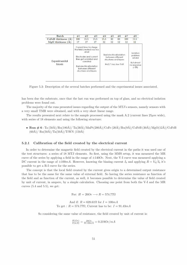
Figure 5.3: Description of the several batches performed and the experimental issues associated.
has been due the substrate, once that the last run was performed on top of glass, and no electrical isolation
problems were found out.
The majority of the runs presented issues regarding the output of the MTJ’s sensors, namely sensors with
a very small TMR were obtained, and with a very short linear range.
The results presented next relate to the sample processed using the mask A.2 (current lines 25μm wide),
with series of 18 elements and using the following structure:
• Run # 6 - Ta (50A)/Ru(180A)/ Ta(30A)/MnPt(200A)/CoFe (20A)/Ru(9A)/CoFeB (30A)/MgO(12A)/CoFeB
(60A)/ Ru(50A)/Ta(50A)/TiWN (150A)
5.2.1 Calibration of the field created by the electrical current
In order to determine the magnetic field created by the electrical current in the paths it was used one of
the test structures: a series of 18 MTJ elements. So first, using the MMS setup, it was measured the MR
curve of the series by applying a field in the range of ±140Oe. Next, the V-I curve was measured applying a
DC current in the range of ±100mA. However, knowing the biasing current Ib and applying R = V0/Ib it’s
possible to get a R-I curve for the series.
The concept is that the local field created by the current gives origin to a determined output resistance
that has to be the same for the same value of external field. So having the series resistance as function of
the field and as function of the current, as well, it becomes possible to determine the value of field created
by unit of current, in ampere, by a simple calculation. Choosing one point from both the V-I and the MR
curves (5.4 and 5.5), we get:
For: H = 20Oe −→ R = 574.77Ω
And if: R = 628.61Ω for I = 100mA
To get : R = 574.77Ω, Current has to be: I = 91.43mA
So considering the same value of resistance, the field created by unit of current is:
H(Oe)I(mA) =
20Oe91.43mA = 0.219Oe/mA
51
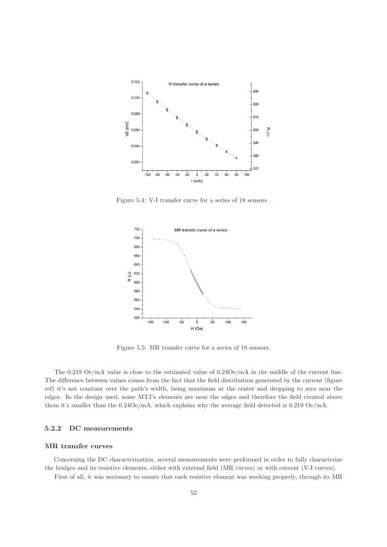
Figure 5.4: V-I transfer curve for a series of 18 sensors .
Figure 5.5: MR transfer curve for a series of 18 sensors.
The 0.219 Oe/mA value is close to the estimated value of 0.24Oe/mA in the middle of the current line.
The difference between values comes from the fact that the field distribution generated by the current (figure
ref) it’s not constant over the path’s width, being maximum at the center and dropping to zero near the
edges. In the design used, some MTJ’s elements are near the edges and therefore the field created above
them it’s smaller than the 0.24Oe/mA, which explains why the average field detected is 0.219 Oe/mA.
5.2.2 DC measurements
MR transfer curves
Concerning the DC characterization, several measurements were performed in order to fully characterize
the bridges and its resistive elements, either with external field (MR curves) or with current (V-I curves).
First of all, it was necessary to ensure that each resistive element was working properly, through its MR
52
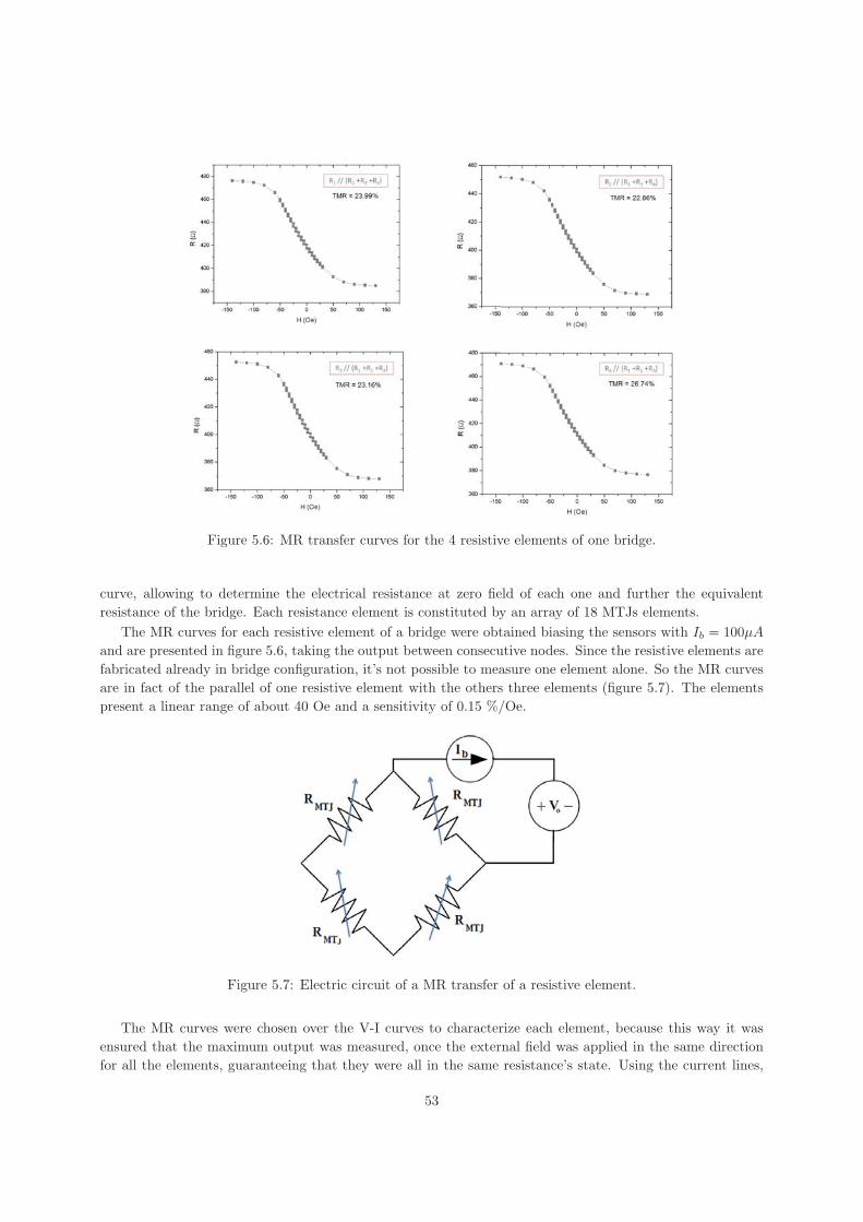
Figure 5.6: MR transfer curves for the 4 resistive elements of one bridge.
curve, allowing to determine the electrical resistance at zero field of each one and further the equivalent
resistance of the bridge. Each resistance element is constituted by an array of 18 MTJs elements.
The MR curves for each resistive element of a bridge were obtained biasing the sensors with Ib = 100μA
and are presented in figure 5.6, taking the output between consecutive nodes. Since the resistive elements are
fabricated already in bridge configuration, it’s not possible to measure one element alone. So the MR curves
are in fact of the parallel of one resistive element with the others three elements (figure 5.7). The elements
present a linear range of about 40 Oe and a sensitivity of 0.15 %/Oe.
Figure 5.7: Electric circuit of a MR transfer of a resistive element.
The MR curves were chosen over the V-I curves to characterize each element, because this way it was
ensured that the maximum output was measured, once the external field was applied in the same direction
for all the elements, guaranteeing that they were all in the same resistance’s state. Using the current lines,
53
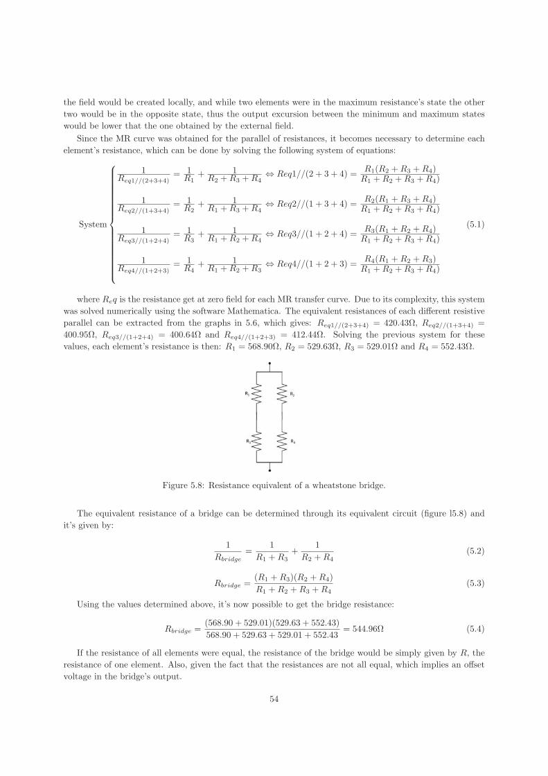
the field would be created locally, and while two elements were in the maximum resistance’s state the other
two would be in the opposite state, thus the output excursion between the minimum and maximum states
would be lower that the one obtained by the external field.
Since the MR curve was obtained for the parallel of resistances, it becomes necessary to determine each
element’s resistance, which can be done by solving the following system of equations:
System
⎧⎪⎪⎪⎪⎪⎪⎪⎪⎪⎪⎪⎪⎪⎪⎪⎪⎨⎪⎪⎪⎪⎪⎪⎪⎪⎪⎪⎪⎪⎪⎪⎪⎪⎩
1Req1//(2+3+4)
= 1R1
+ 1R2 +R3 +R4
⇔ Req1//(2 + 3 + 4) =R1(R2 +R3 +R4)R1 +R2 +R3 +R4)
1Req2//(1+3+4)
= 1R2
+ 1R1 +R3 +R4
⇔ Req2//(1 + 3 + 4) =R2(R1 +R3 +R4)R1 +R2 +R3 +R4)
1Req3//(1+2+4)
= 1R3
+ 1R1 +R2 +R4
⇔ Req3//(1 + 2 + 4) =R3(R1 +R2 +R4)R1 +R2 +R3 +R4)
1Req4//(1+2+3)
= 1R4
+ 1R1 +R2 +R3
⇔ Req4//(1 + 2 + 3) =R4(R1 +R2 +R3)R1 +R2 +R3 +R4)
(5.1)
where Req is the resistance get at zero field for each MR transfer curve. Due to its complexity, this system
was solved numerically using the software Mathematica. The equivalent resistances of each different resistive
parallel can be extracted from the graphs in 5.6, which gives: Req1//(2+3+4) = 420.43Ω, Req2//(1+3+4) =
400.95Ω, Req3//(1+2+4) = 400.64Ω and Req4//(1+2+3) = 412.44Ω. Solving the previous system for these
values, each element’s resistance is then: R1 = 568.90Ω, R2 = 529.63Ω, R3 = 529.01Ω and R4 = 552.43Ω.
Figure 5.8: Resistance equivalent of a wheatstone bridge.
The equivalent resistance of a bridge can be determined through its equivalent circuit (figure l5.8) and
it’s given by:
1
Rbridge=
1
R1 +R3+
1
R2 +R4(5.2)
Rbridge =(R1 +R3)(R2 +R4)
R1 +R2 +R3 +R4(5.3)
Using the values determined above, it’s now possible to get the bridge resistance:
Rbridge =(568.90 + 529.01)(529.63 + 552.43)
568.90 + 529.63 + 529.01 + 552.43= 544.96Ω (5.4)
If the resistance of all elements were equal, the resistance of the bridge would be simply given by R, the
resistance of one element. Also, given the fact that the resistances are not all equal, which implies an offset
voltage in the bridge’s output.
54
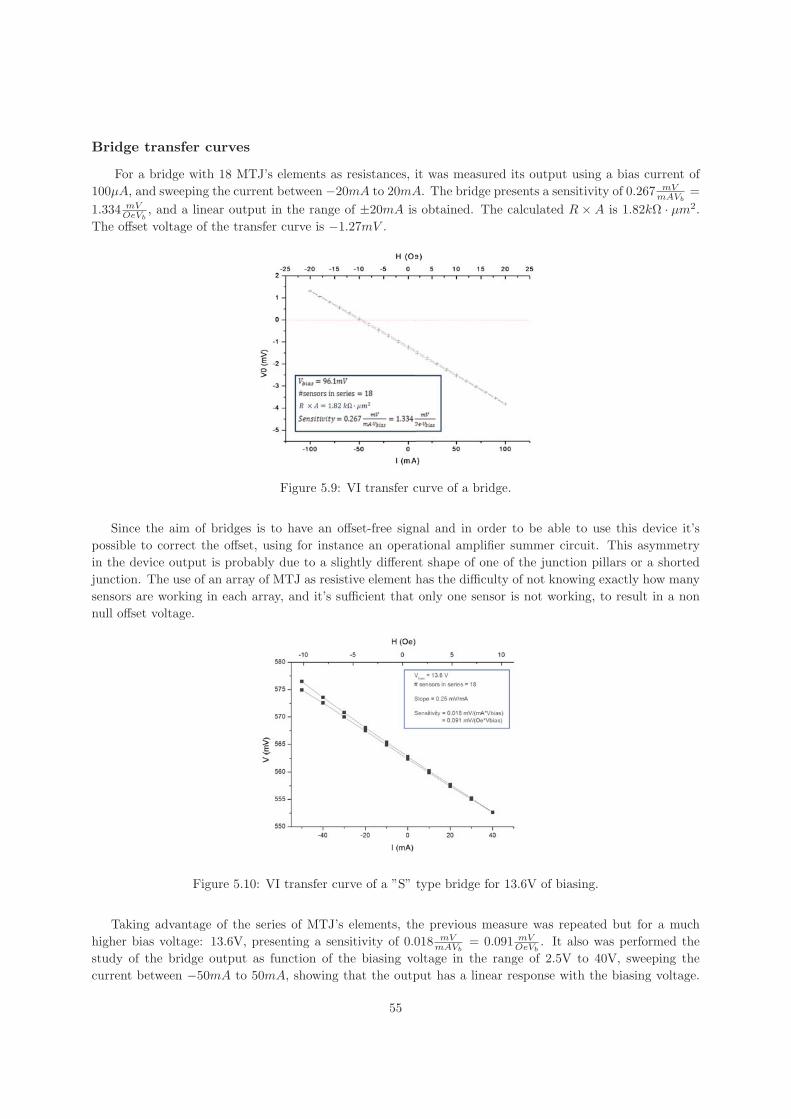
Bridge transfer curves
For a bridge with 18 MTJ’s elements as resistances, it was measured its output using a bias current of
100μA, and sweeping the current between −20mA to 20mA. The bridge presents a sensitivity of 0.267 mVmAVb
=
1.334 mVOeVb
, and a linear output in the range of ±20mA is obtained. The calculated R × A is 1.82kΩ · μm2.
The offset voltage of the transfer curve is −1.27mV .
Figure 5.9: VI transfer curve of a bridge.
Since the aim of bridges is to have an offset-free signal and in order to be able to use this device it’s
possible to correct the offset, using for instance an operational amplifier summer circuit. This asymmetry
in the device output is probably due to a slightly different shape of one of the junction pillars or a shorted
junction. The use of an array of MTJ as resistive element has the difficulty of not knowing exactly how many
sensors are working in each array, and it’s sufficient that only one sensor is not working, to result in a non
null offset voltage.
Figure 5.10: VI transfer curve of a ”S” type bridge for 13.6V of biasing.
Taking advantage of the series of MTJ’s elements, the previous measure was repeated but for a much
higher bias voltage: 13.6V, presenting a sensitivity of 0.018 mVmAVb
= 0.091 mVOeVb
. It also was performed the
study of the bridge output as function of the biasing voltage in the range of 2.5V to 40V, sweeping the
current between −50mA to 50mA, showing that the output has a linear response with the biasing voltage.
55
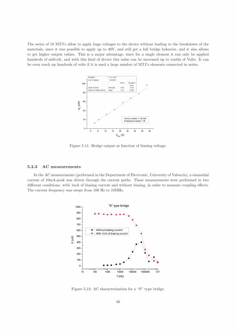
The series of 18 MTJ’s allow to apply huge voltages to the device without leading to the breakdown of the
materials, since it was possible to apply up to 40V, and still get a full bridge behavior, and it also allows
to get higher output values. This is a major advantage, since for a single element it can only be applied
hundreds of milivolt, and with this kind of device this value can be increased up to tenths of Volts. It can
be even reach up hundreds of volts if it is used a large number of MTJ’s elements connected in series.
Figure 5.11: Bridge output as function of biasing voltage.
5.2.3 AC measurements
In the AC measurements (performed in the Department of Electronic, University of Valencia), a sinusoidal
current of 10mA-peak was driven through the current paths. These measurements were performed in two
different conditions: with 1mA of biasing current and without biasing, in order to measure coupling effects.
The current frequency was swept from 100 Hz to 10MHz.
Figure 5.12: AC characterization for a “S” type bridge.
56
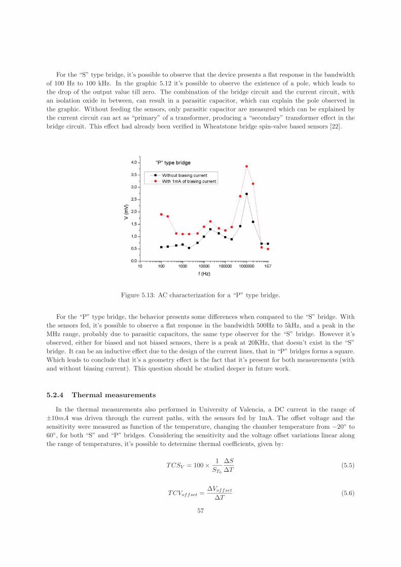
For the “S” type bridge, it’s possible to observe that the device presents a flat response in the bandwidth
of 100 Hz to 100 kHz. In the graphic 5.12 it’s possible to observe the existence of a pole, which leads to
the drop of the output value till zero. The combination of the bridge circuit and the current circuit, with
an isolation oxide in between, can result in a parasitic capacitor, which can explain the pole observed in
the graphic. Without feeding the sensors, only parasitic capacitor are measured which can be explained by
the current circuit can act as “primary” of a transformer, producing a “secondary” transformer effect in the
bridge circuit. This effect had already been verified in Wheatstone bridge spin-valve based sensors [22].
Figure 5.13: AC characterization for a “P” type bridge.
For the “P” type bridge, the behavior presents some differences when compared to the “S” bridge. With
the sensors fed, it’s possible to observe a flat response in the bandwidth 500Hz to 5kHz, and a peak in the
MHz range, probably due to parasitic capacitors, the same type observer for the “S” bridge. However it’s
observed, either for biased and not biased sensors, there is a peak at 20KHz, that doesn’t exist in the “S”
bridge. It can be an inductive effect due to the design of the current lines, that in “P” bridges forms a square.
Which leads to conclude that it’s a geometry effect is the fact that it’s present for both measurements (with
and without biasing current). This question should be studied deeper in future work.
5.2.4 Thermal measurements
In the thermal measurements also performed in University of Valencia, a DC current in the range of
±10mA was driven through the current paths, with the sensors fed by 1mA. The offset voltage and the
sensitivity were measured as function of the temperature, changing the chamber temperature from −20◦ to
60◦, for both “S” and “P” bridges. Considering the sensitivity and the voltage offset variations linear along
the range of temperatures, it’s possible to determine thermal coefficients, given by:
TCSV = 100× 1
ST0
ΔS
ΔT(5.5)
TCVoffset =ΔVoffset
ΔT(5.6)
57
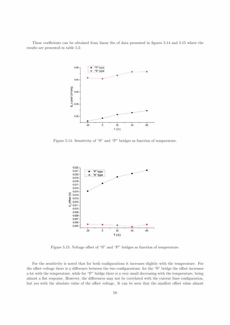
These coefficients can be obtained from linear fits of data presented in figures 5.14 and 5.15 where the
results are presented in table 5.2.
Figure 5.14: Sensitivity of “S” and “P” bridges as function of temperature.
Figure 5.15: Voltage offset of “S” and “P” bridges as function of temperature.
For the sensitivity is noted that for both configurations it increases slightly with the temperature. For
the offset voltage there is a difference between the two configurations: for the “S” bridge the offset increases
a lot with the temperature, while for “P” bridge there is a very small decreasing with the temperature, being
almost a flat response. However, the differences may not be correlated with the current lines configuration,
but yes with the absolute value of the offset voltage. It can be seen that the smallest offset value almost
58

doesn’t change, while for the highest one, it has a huge variation with the temperature, like an amplification
effect.
Table 5.2: Thermal coefficients
“S” bridge “P” bridge
TCSV (%/◦ C) 0.185 0.086
TCVoffset (μV /◦ C) 75.3 -3.8
59

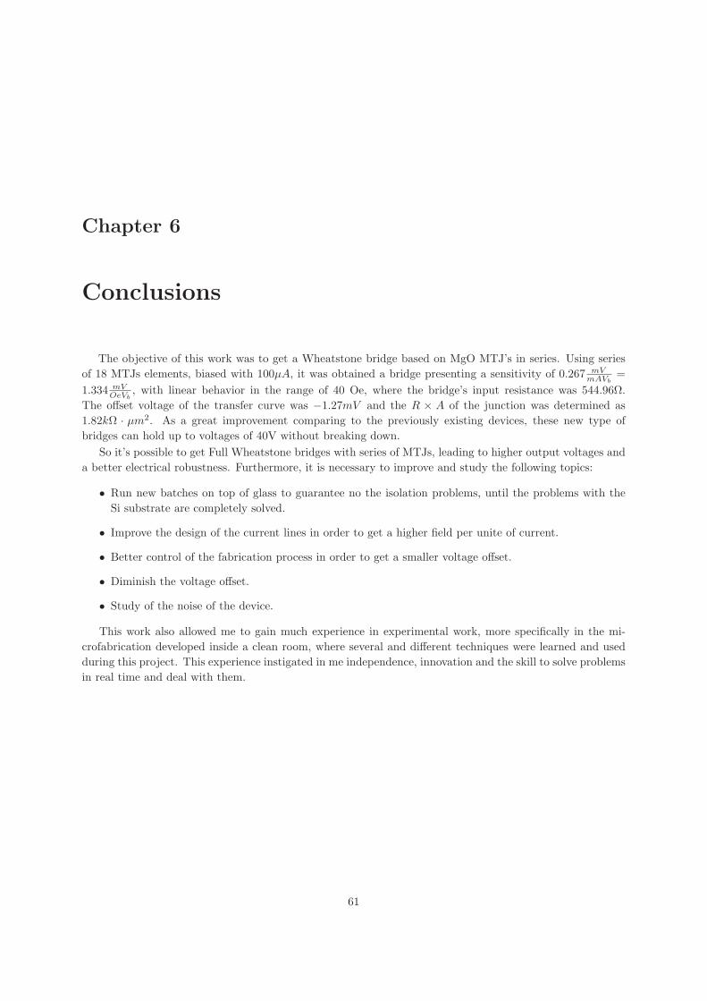
Chapter 6
Conclusions
The objective of this work was to get a Wheatstone bridge based on MgO MTJ’s in series. Using series
of 18 MTJs elements, biased with 100μA, it was obtained a bridge presenting a sensitivity of 0.267 mVmAVb
=
1.334 mVOeVb
, with linear behavior in the range of 40 Oe, where the bridge’s input resistance was 544.96Ω.
The offset voltage of the transfer curve was −1.27mV and the R × A of the junction was determined as
1.82kΩ · μm2. As a great improvement comparing to the previously existing devices, these new type of
bridges can hold up to voltages of 40V without breaking down.
So it’s possible to get Full Wheatstone bridges with series of MTJs, leading to higher output voltages and
a better electrical robustness. Furthermore, it is necessary to improve and study the following topics:
• Run new batches on top of glass to guarantee no the isolation problems, until the problems with the
Si substrate are completely solved.
• Improve the design of the current lines in order to get a higher field per unite of current.
• Better control of the fabrication process in order to get a smaller voltage offset.
• Diminish the voltage offset.
• Study of the noise of the device.
This work also allowed me to gain much experience in experimental work, more specifically in the mi-
crofabrication developed inside a clean room, where several and different techniques were learned and used
during this project. This experience instigated in me independence, innovation and the skill to solve problems
in real time and deal with them.
61


Bibliography
[1] Hitchhikers’s guide to magnetism, Institute of Rock Magnetism, University of Minnesota, June 1991.
Web. 7 Oct. 2010. < http://www.irm.umn.edu/hg2m/hg2m index.html >
[2] S.O. Kasap, Principles of Electronic Materials and Devices, McGraw-Hill, 2nd edition, 2006.
[3] R. Waser, Nanoelectronics and information technology: advanced electronic materials and novel devices,
Wiley-VCH, 2nd edition, 2005.
[4] HyperPhysics, Carl R. Nave, Department of Physics and Astronomy, Georgia State University, 2001.
Web. 7 Oct. 2010 < http://hyperphysics.phy-astr.gsu.edu/hbase/hph.html >
[5] A. Fert, et al., Giant Magnetoresistance of (001)Fe/(001)Cr Magnetic Superlattices,Phys. Rev. Letter
61(21): 2472-2475, 1988.
[6] B. Dieny, et al., Giant magnetoresistance in soft ferromagnetic multilayers, Phys. Rev. B 43(1): 1297-
1300, 1991.
[7] M. Julliere, Tunneling between ferromagnetic films, Phys. Lett. A 54: 225, 1975.
[8] P. Grunberg, et al., Enhanced Magnetoresistance in layered magnetic structures with antiferromagnetic
interlayer exchange, Phys. Rev. B 39(7): 4828-4830, 1989.
[9] J. C. Slonczewski, Conductance and exchange coupling of two ferromagnets separated by a tunneling
barrier, Phys. Rev. B 39: 6995, 1989.
[10] D. Wang, et al., Spin dependent tunneling junctions with reduce Neel coupling, J.Appl.Phys., 93(10),
2002.
[11] P. Bruno, C. Chappert, Giant Magnetoresistance of (001)Fe/(001)Cr Magnetic Superlattices,Phys. Rev.
Letter 67: 1602, 1991.
[12] P.Wisniowski, et al., Effect of free layer thickness and shape anisotropy on the transfer curves of MgO
magnetic tunnel junctions, J.Appl.Phys. 103, 07A910, 2008.
[13] Manuel Joao de Moura Dias Mendes, Micromagnetic Simulations of Spin Valve devices, Senior thesis,
Instituto Superior Tecnico, 2005.
[14] Susana Isabel Pinheiro Cardoso de Freitas, Dual-Stripe GMR and Tunnel Junction Read Heads and Ion
Beam Deposition and Oxidation of Tunnel Junctions, PhD thesis, Instituto Superior Tecnico, 2001.
[15] Ricardo Alexandre de Matos Antunes Ferreira, Ion Beam Deposited Magnetic Spin Tunnel Junctions
targeting HDD Read Heads, Non-volatile Memories and Magnetic Field Sensor Applications, PhD the-
sis, Instituto Superior Tecnico, 2008.
63

[16] N. Hasegawa, et al., Nano-oxide-layer specular spin valve heads with synthetic pinned layer: Head
performance and reliability, J.Appl.Phys. 91(10): 8774, 2002.
[17] Jianguo Wang, Low-resistance tunnel junctions for read head applications, PhD thesis, Instituto Supe-
rior Tecnico, 2002.
[18] Haohua Li, Spin valve read elements and sensors, PhD thesis, Instituto Superior Tecnico, 2004.
[19] S. Ekelof, The Genesis of the Wheatstone Bridge, Engineering Science and Education Journal, 10(1):
37-40,2001.
[20] C Reig, et al., GMR Based Electrical Current Sensors, Giant Magnetoresistance: New Research. Nova
Science Publishers, Inc., 239-275, 2008.
[21] C Reig, et al., Electrical Isolators Based on Tunneling Magnetoresistance Technology, IEEE Transac-
tions on Magnetics, 44: 4011-4014, 2008.
[22] M.D. Cubells-Beltran, et al., Full Wheatstone bridge spin-valve based sensors for IC currents monitor-
ing, IEEE Sensors Journals 9(12): 239-275, 2008.
[23] C. Reig, et al., Magnetic Field Sensors Based on Giant Magnetoresistance (GMR) Technology: Appli-
cations in Electrical Current Sensing, Sensors, 9: 7919-7942, 2009.
[24] J. Cao and P.P. Freitas, Wheatstone bridge sensor composed of linear MgO magnetic tunnel junction,
Jounal of Applied Physics, Vol. 107, 2010.
[25] Ricardo Alves Ferreira Costa e Sousa, Magnetic Random Access Memory (MRAM) based on Spin
Dependent Tunnel Junctions, PhD thesis, Instituto Superior Tecnico.
[26] H. N. Bertram, Theory of Magnetic Recording, Cambridge University Press, 1994.
[27] R. Guerrero, et al., Low frequency noise in arrays of magnetic tunnel junctions connected in series and
parallel, Appl. Phys., Vol. 105, 2009.
64
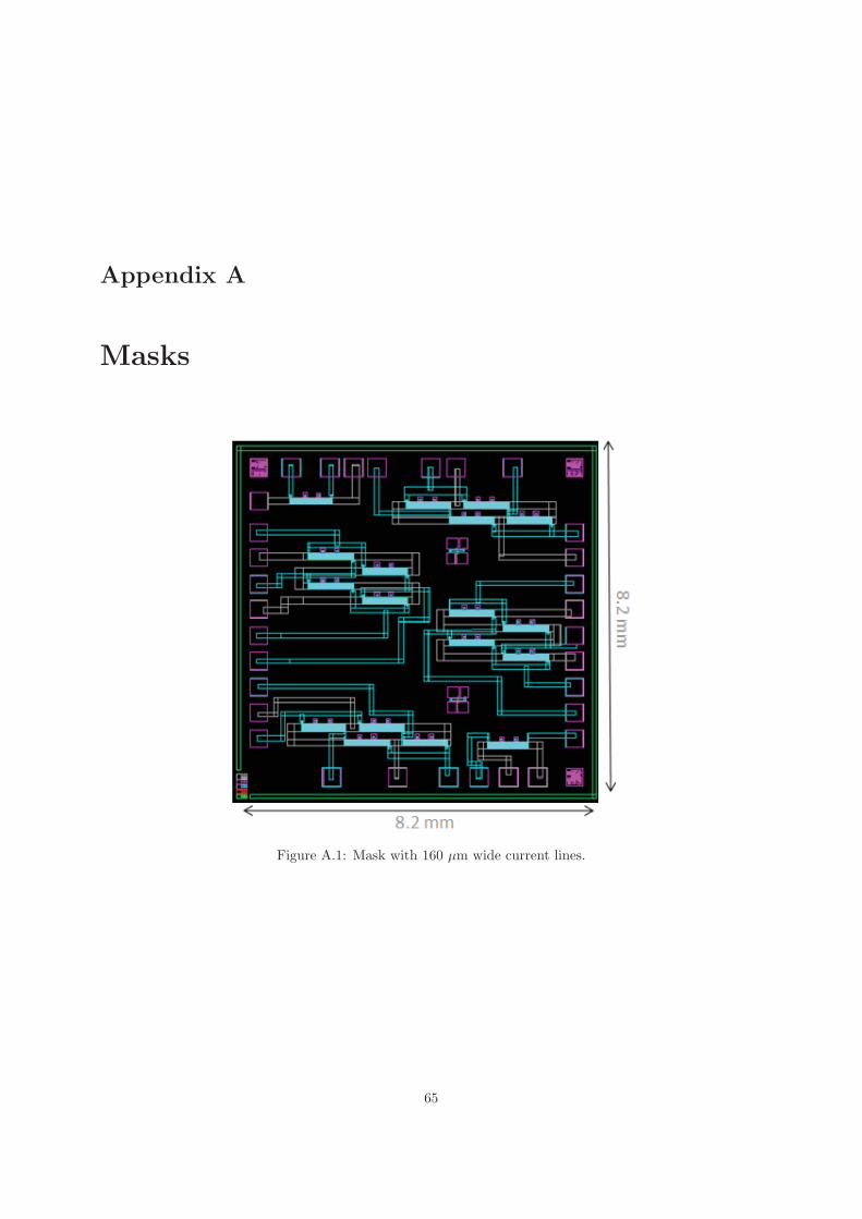
Appendix A
Masks
Figure A.1: Mask with 160 μm wide current lines.
65
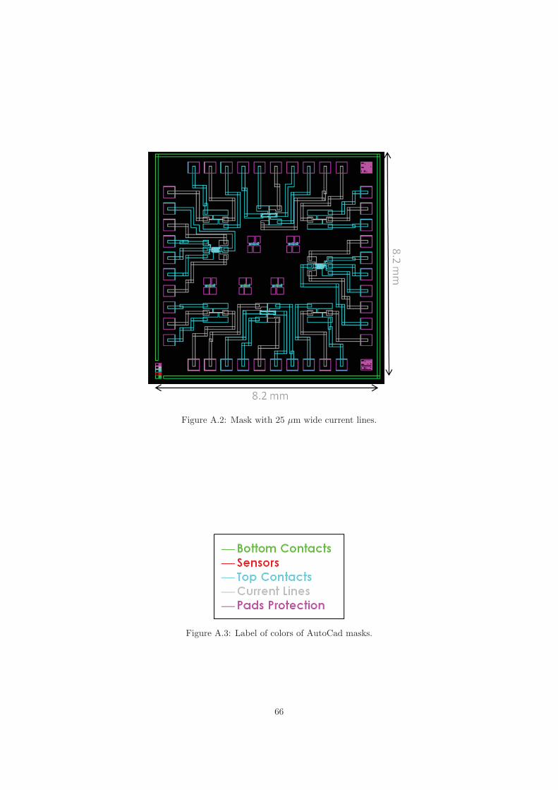
Figure A.2: Mask with 25 μm wide current lines.
Figure A.3: Label of colors of AutoCad masks.
66

67
Appendix B
Run Sheet
RUN:
Process Start : ___ / ___ / ___ Process Finish : ___ / ___ / ___
Si/SiO2 (1000 Å) substrate 1x1 inch2
Machine: Nordiko 2000
Comments: Bottom electrode: Ta 50 Å/ Ru 180 Å/ Ta 30 Å/ PtMn 200 Å/ CoFe 20 Å/ Ru 9 Å/ CoFeB 30 Å
Tunnel junction structure: MgO x Å
Top electrode: CoFeB y Å/ Ru 50 Å/ Ta 50 Å
Total height: 619 Å + x + y
Calibration samples: VSM, Top electrode for 2nd etch (glass substrate)
Characterization: VSM (Applied Field Range: -6000 to 6000 Oe) after annealed (at 320º under 4kOe for
1hour)
Machine: Nordiko 7000
Seq.17 – mod.2 – f.9 (1’ soft sputter etch) P=60W/40W, p=3mTorr, 50 sccm Ar
mod 3 – f.19 (150A TiW, 27’’) P=0.5 kW, 3mTorr, 50sccm Ar + 10 sccm N2
Readings – Module 2
Run# Power1 Power2 Gas flux Pressure
F59R8B1 F40R1 50.2 sccm Ar 3.1mTorr
Readings – Module 3
Run# Power Voltage Current Gas flux Pressure
0.5kW 419V 1.2A (50.5 Ar +10.6 N2)sccm 3.0 mTorr
Calibration samples: Top electrode for 2nd etch
STEP 1 Tunnel Junction Deposition Date: ___ / ___ / ___
STEP 2 TMR passivation – 150 Å TiWN2 Date: ___ / ___ / ___
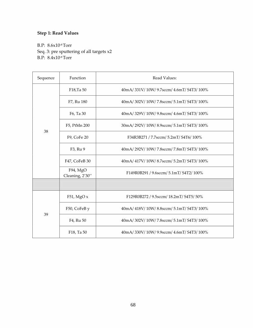
68
Step 1: Read Values
B.P: 8.6x10⁻⁸ Torr
Seq. 3: pre sputtering of all targets x2
B.P: 8.4x10⁻⁸ Torr
Sequence Function Read Values:
38
F18,Ta 50 40mA/ 331V/ 10W/ 9.7sccm/ 4.6mT/ S4T3/ 100%
F7, Ru 180 40mA/ 302V/ 10W/ 7.8sccm/ 5.1mT/ S4T3/ 100%
F6, Ta 30 40mA/ 329V/ 10W/ 9.8sccm/ 4.6mT/ S4T3/ 100%
F5, PtMn 200 30mA/ 292V/ 10W/ 8.9sccm/ 5.1mT/ S4T3/ 100%
F9, CoFe 20 F34R3B271 / 7.7sccm/ 5.2mT/ S4T6/ 100%
F3, Ru 9 40mA/ 292V/ 10W/ 7.8sccm/ 7.8mT/ S4T3/ 100%
F47, CoFeB 30 40mA/ 417V/ 10W/ 8.7sccm/ 5.2mT/ S4T3/ 100%
F94, MgO
Cleaning, 2’30’’ F149R0B291 / 9.6sccm/ 5.1mT/ S4T2/ 100%
39
F51, MgO x F129R0B272 / 9.5sccm/ 18.2mT/ S4T5/ 50%
F50, CoFeB y 40mA/ 418V/ 10W/ 8.8sccm/ 5.1mT/ S4T3/ 100%
F4, Ru 50 40mA/ 302V/ 10W/ 7.8sccm/ 5.1mT/ S4T3/ 100%
F18, Ta 50 40mA/ 330V/ 10W/ 9.9sccm/ 4.6mT/ S4T3/ 100%
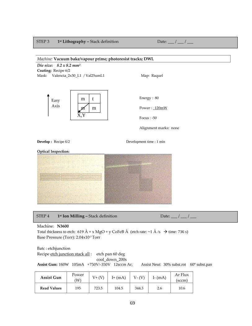
69
Machine: Vacuum bake/vapour prime; photoresist tracks; DWL
Die size: 8.2 x 8.2 mm2 Coating: Recipe 6/2
Mask: Valencia_2x30_L1 / Val25umL1 Map: Raquel
Energy : 80
Power : _120mW
Focus : -50
Alignment marks: none
Develop : Recipe 6/2 Development time : 1 min
Optical Inspection:
Machine: N3600
Total thickness to etch: 619 Å + x MgO + y CoFeB Å (etch rate: ~1 Å /s time: 736 s) Base Pressure (Torr): 2.04x10⁻⁷ Torr
Batc : etchjunction
Recipe etch junction stack all : etch pan 60 deg
cool_down_200s Assist Gun: 160W 105mA +750V/-350V 12sccm Ar; Assist Neut: 30% subst.rot 60º subst.pan
Assist Gun Power
(W) V+ (V) I+ (mA) V- (V) I- (mA)
Ar Flux
(sccm)
Read Values 195 723.5 104.5 344.3 2.6 10.6
STEP 3 1st Lithography – Stack definition Date: ___ / ___ / ___
STEP 4 1st Ion Milling – Stack definition Date: ___ / ___ / ___
Easy
Axis
m t
m m
X,Y
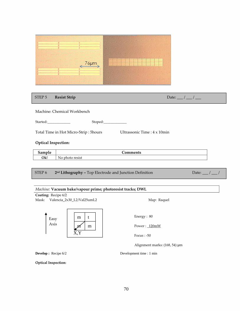
70
Machine: Chemical Workbench
Started:_____________ Stoped:_____________
Total Time in Hot Micro-Strip : 5hours Ultrassonic Time : 4 x 10min
Optical Inspection:
Sample Comments
Ok! No photo resist
Machine: Vacuum bake/vapour prime; photoresist tracks; DWL
Coating: Recipe 6/2
Mask: Valencia_2x30_L2 /Val25umL2 Map: Raquel
Energy : 80
Power : _120mW
Focus : -50
Alignment marks: (168, 54) μm
Develop : Recipe 6/2 Development time : 1 min
Optical Inspection:
STEP 5 Resist Strip Date: ___ / ___ / ___
STEP 6 2nd Lithography – Top Electrode and Junction Definition Date: ___ / ___ /
___
Easy
Axis
m t
m m
X,Y
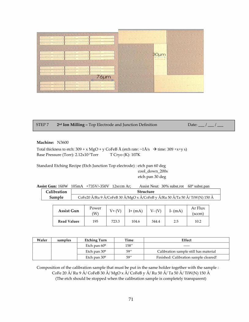
71
Machine: N3600
Total thickness to etch: 309 + x MgO + y CoFeB Å (etch rate: ~1Å/s time: 309 +x+y s)
Base Pressure (Torr): 2.12x10⁻⁷Torr T Cryo (K): 107K
Standard Etching Recipe (Etch Junction Top electrode) : etch pan 60 deg
cool_down_200s
etch pan 30 deg
Assist Gun: 160W 105mA +735V/-350V 12sccm Ar; Assist Neut: 30% subst.rot 60º subst.pan
Calibration
Sample
Structure
CoFe20 Å/Ru 9 Å/CoFeB 30 Å/MgO x Å/CoFeB y Å/Ru 50 Å/Ta 50 Å/ TiW(N) 150 Å
Assist Gun Power
(W) V+ (V) I+ (mA) V- (V) I- (mA)
Ar Flux
(sccm)
Read Values 195 723.3 104.6 344.4 2.5 10.2
Wafer samples Etching Turn Time Effect
Etch pan 60º 158’’ -----
Etch pan 30º 59’’ Calibration sample still has material
Etch pan 30º 59’’ Finished: Calibration sample cleared!
Composition of the calibration sample that must be put in the same holder together with the sample :
CoFe 20 Å/ Ru 9 Å/ CoFeB 30 Å/ MgO x Å/ CoFeB y Å/ Ru 50 Å/ Ta 50 Å/ TiW(N) 150 Å
(The etch should be stopped when the calibration sample is completely transparent)
STEP 7 2nd Ion Milling – Top Electrode and Junction Definition Date: ___ / ___ / ___

72
Responsible: Fernando
Machine: UHV2
Dep. Rate ~11.43 Å/min
Deposition
Time
Al2O3 thickness Ar gas flow Pressure Power Source
62min 700 Å 45 sccm 3.0 mTorr 200W
Comments: Calibration sample (profilometer and ellipsometer)
Ellipsometer Δ Ψ TU NU
73.79 31.49 688 1.635
Profilometer
a (Å) b (Å) h (Å) h medio
63 -581 644
(631.25 ± 33)Å 640 -4 644
321 -318 639
-378 220 598
Machine: Chemical Workbench
Started:_____________ Stoped:_____________
Total Time in Hot Micro-Strip : 4days Ultrassonic Time : 3x10min
Optical Inspection:
STEP 8 Insulating Layer Deposition Date: ___ / ___ / ___
STEP 9 Oxide Lift-Off Date: ___ / ___ / ___
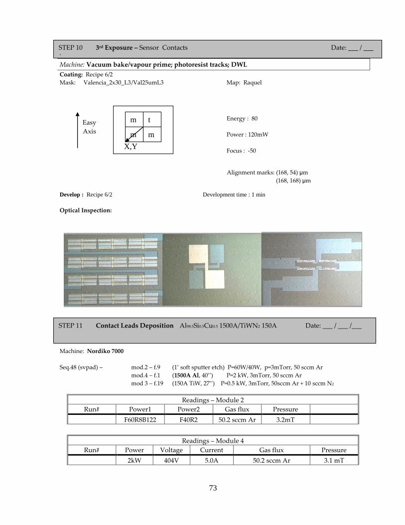
73
Machine: Vacuum bake/vapour prime; photoresist tracks; DWL
Coating: Recipe 6/2
Mask: Valencia_2x30_L3 /Val25umL3 Map: Raquel
Energy : 80
Power : 120mW
Focus : -50
Alignment marks: (168, 54) μm
(168, 168) μm
Develop : Recipe 6/2 Development time : 1 min
Optical Inspection:
Machine: Nordiko 7000
Seq.48 (svpad) – mod.2 – f.9 (1’ soft sputter etch) P=60W/40W, p=3mTorr, 50 sccm Ar
mod.4 – f.1 (1500A Al, 40’’) P=2 kW, 3mTorr, 50 sccm Ar
mod 3 – f.19 (150A TiW, 27’’) P=0.5 kW, 3mTorr, 50sccm Ar + 10 sccm N2
Readings – Module 2
Run# Power1 Power2 Gas flux Pressure
F60R8B122 F40R2 50.2 sccm Ar 3.2mT
Readings – Module 4
Run# Power Voltage Current Gas flux Pressure
2kW 404V 5.0A 50.2 sccm Ar 3.1 mT
STEP 11 Contact Leads Deposition Al98.5Si0.5Cu0.5 1500A/TiWN2 150A Date: ___ / ___ /___
STEP 10 3rd Exposure – Sensor Contacts Date: ___ / ___
/ ___
Easy
Axis
m t
m m
X,Y
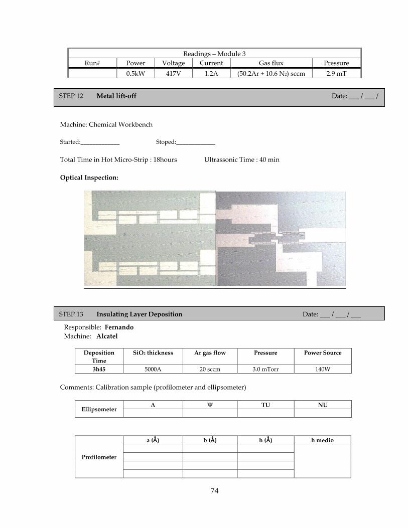
74
Readings – Module 3
Run# Power Voltage Current Gas flux Pressure
0.5kW 417V 1.2A (50.2Ar + 10.6 N2) sccm 2.9 mT
Machine: Chemical Workbench
Started:_____________ Stoped:_____________
Total Time in Hot Micro-Strip : 18hours Ultrassonic Time : 40 min
Optical Inspection:
Responsible: Fernando
Machine: Alcatel
Deposition
Time
SiO2 thickness Ar gas flow Pressure Power Source
3h45 5000A 20 sccm 3.0 mTorr 140W
Comments: Calibration sample (profilometer and ellipsometer)
Ellipsometer Δ Ψ TU NU
Profilometer
a (Å) b (Å) h (Å) h medio
STEP 12 Metal lift-off Date: ___ / ___ /
___
STEP 13 Insulating Layer Deposition Date: ___ / ___ / ___
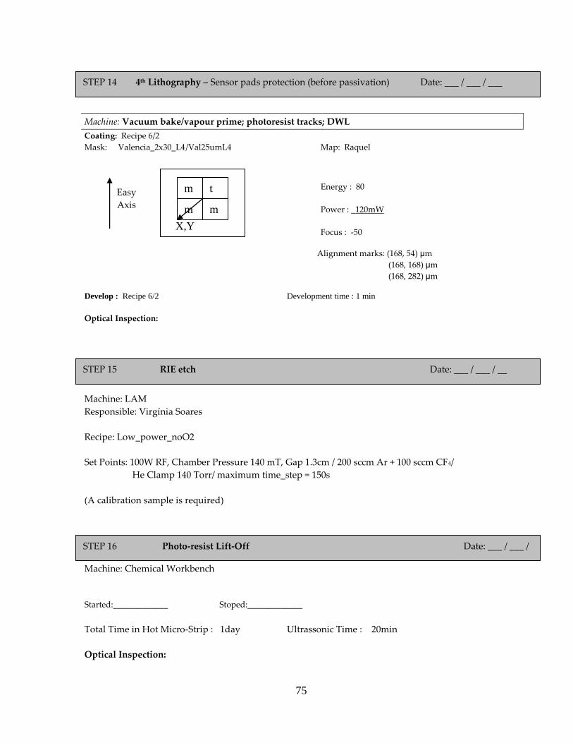
75
Machine: Vacuum bake/vapour prime; photoresist tracks; DWL
Coating: Recipe 6/2
Mask: Valencia_2x30_L4 /Val25umL4 Map: Raquel
Energy : 80
Power : _120mW
Focus : -50
Alignment marks: (168, 54) μm
(168, 168) μm
(168, 282) μm
Develop : Recipe 6/2 Development time : 1 min
Optical Inspection:
Machine: LAM
Responsible: Virgínia Soares
Recipe: Low_power_noO2
Set Points: 100W RF, Chamber Pressure 140 mT, Gap 1.3cm / 200 sccm Ar + 100 sccm CF4/
He Clamp 140 Torr/ maximum time_step = 150s
(A calibration sample is required)
Machine: Chemical Workbench
Started:_____________ Stoped:_____________
Total Time in Hot Micro-Strip : 1day Ultrassonic Time : 20min
Optical Inspection:
STEP 15 RIE etch Date: ___ / ___ / __
Machine: Chemical Workbench
Started:_____________ Stoped:_____________
Total Time in Hot Micro-Strip : __________ Ultrassonic Time : ________________
Optical Inspection:
Machine: Chemical Workbench
Started:_____________ Stoped:_____________
Total Time in Hot Micro-Strip : __________ Ultrassonic Time : ________________
Optical Inspection:
Machine: Chemical Workbench
Started:_____________ Stoped:_____________
STEP 14 4th Lithography – Sensor pads protection (before passivation) Date: ___ / ___ / ___
Easy
Axis
m t
m m
X,Y
STEP 16 Photo-resist Lift-Off Date: ___ / ___ /
__
Machine: Chemical Workbench
Started:_____________ Stoped:_____________
Total Time in Hot Micro-Strip : __________ Ultrassonic Time : ________________
Optical Inspection:
Machine: Chemical Workbench
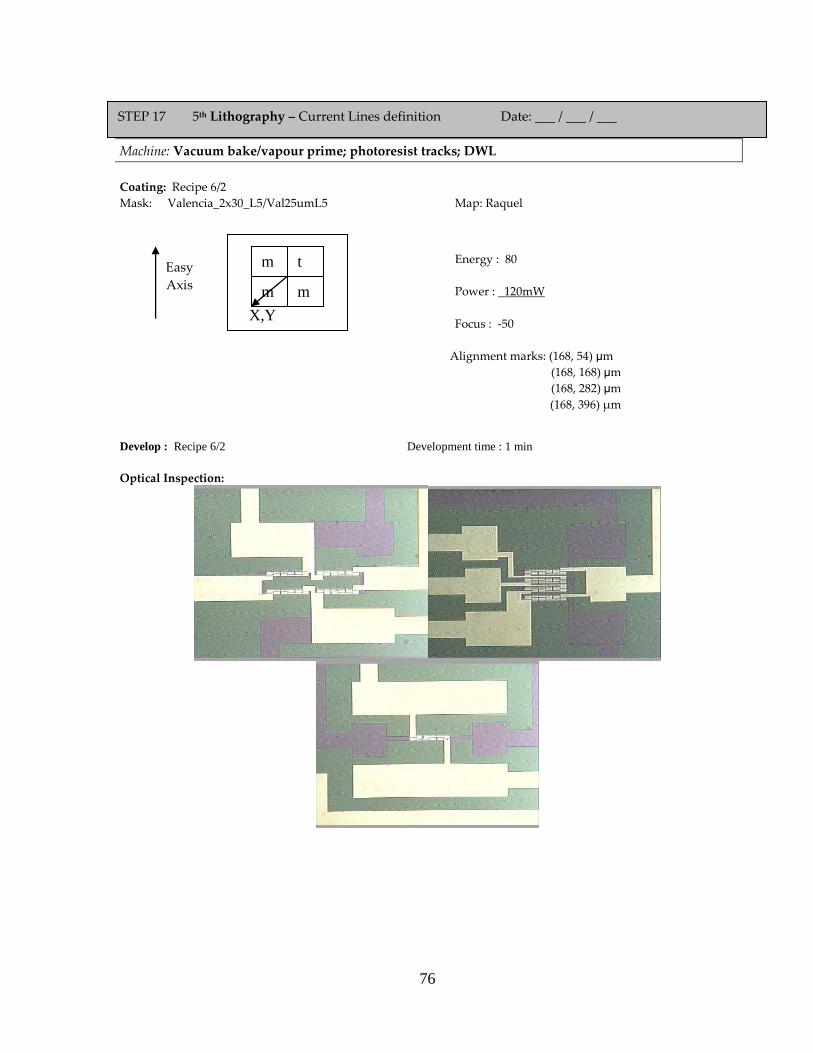
76
Machine: Vacuum bake/vapour prime; photoresist tracks; DWL
Coating: Recipe 6/2
Mask: Valencia_2x30_L5/Val25umL5 Map: Raquel
Energy : 80
Power : _120mW
Focus : -50
Alignment marks: (168, 54) μm
(168, 168) μm
(168, 282) μm
(168, 396) μm
Develop : Recipe 6/2 Development time : 1 min
Optical Inspection:
STEP 17 5th Lithography – Current Lines definition Date: ___ / ___ / ___
Easy
Axis
m t
m m
X,Y
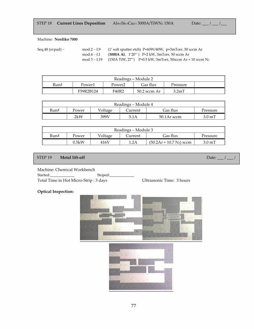
77
Machine: Nordiko 7000
Seq.48 (svpad) – mod.2 – f.9 (1’ soft sputter etch) P=60W/40W, p=3mTorr, 50 sccm Ar
mod.4 – f.1 (3000A Al, 1’20’’ ) P=2 kW, 3mTorr, 50 sccm Ar
mod 3 – f.19 (150A TiW, 27’’) P=0.5 kW, 3mTorr, 50sccm Ar + 10 sccm N2
Readings – Module 2
Run# Power1 Power2 Gas flux Pressure
F59R2B124 F40R2 50.2 sccm Ar 3.2mT
Readings – Module 4
Run# Power Voltage Current Gas flux Pressure
2kW 399V 5.1A 50.1Ar sccm 3.0 mT
Readings – Module 3
Run# Power Voltage Current Gas flux Pressure
0.5kW 416V 1.2A (50.2Ar + 10.7 N2) sccm 3.0 mT
Machine: Chemical Workbench Started:_____________ Stoped:_____________
Total Time in Hot Micro-Strip : 3 days Ultrassonic Time: 3 hours
Optical Inspection:
STEP 18 Current Lines Deposition Al98.5Si0.5Cu0.5 3000A/TiWN2 150A Date: ___ / ___ /___
STEP 19 Metal lift-off Date: ___ / ___ /
___

78
Responsible: Fernando
Machine: Alcatel
Deposition
Time
Al2O3 thickness Ar gas flow Pressure Power Source
2000A 45 sccm 200W
Comments: Calibration sample (profilometer and ellipsometer)
Ellipsometer Δ Ψ TU NU
Profilometer
a (Å) b (Å) h (Å) h medio
Machine: Vacuum bake/vapour prime; photoresist tracks; DWL
Coating: Recipe 6/2
Mask: Valencia_2x30_L6 /Val25umL6 Map: Raquel
Energy : 80
Power : _120mW
Focus : -50
Alignment marks: (168, 54) μm
(168, 168) μm
(168, 282) μm
(168, 396) μm
(168, 510) μm
Develop : Recipe 6/2 Development time : 1 min
Optical Inspection:
STEP 21 6th Exposure – Pads protection Date: ___ / ___ / ___
Easy
Axis
m t
m m
X,Y
STEP 20 Passivation (2000 A SiO2) Date: ___ / ___ / ___

79
Machine: LAM
Responsible: Virgínia Soares
Recipe: Low_power_noO2
Set Points: 100W RF, Chamber Pressure 140 mT, Gap 1.3cm / 200 sccm Ar + 100 sccm CF4/
He Clamp 140 Torr/ maximum time_step = 150s
(A calibration sample is required)
Hot μ-strip + ultrasonic
Rinse with IPA + DI water + dry compressed air
Started:_____________ Stoped:_____________
Total Time in hot μ-strip : 4hours Ultrasonic Time : 20 min
Optical inspection:
Setup: Old annealing setup
Temperature: 320ºC real (corresponds to 280 ºC as setpoint)
Annealing Time: 1h
H Field: 4kOe
STEP 22 RIE Etch (2000 A Al2O3) Date: ___ / ___ /___
STEP 23 Oxide lift-off Date: ___ / ___ /
___
STEP 24 Anneal Date: ___ / ___ / ___