
Metallization Technologies on a Smooth Resin Surface for ... · Metallization Technologies on a...
6
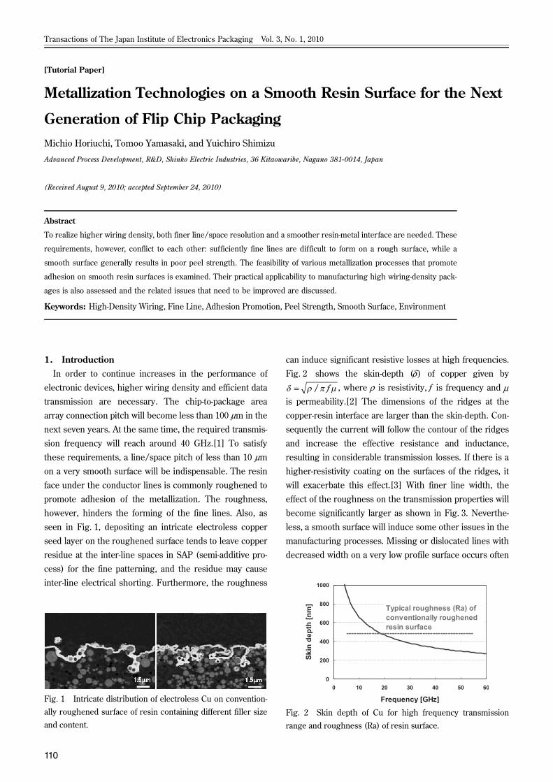
110 Transactions of The Japan Institute of Electronics Packaging Vol. 3, No. 1, 2010 [Tutorial Paper] Metallization Technologies on a Smooth Resin Surface for the Next Generation of Flip Chip Packaging Michio Horiuchi, Tomoo Yamasaki, and Yuichiro Shimizu Advanced Process Development, R&D, Shinko Electric Industries, 36 Kitaowaribe, Nagano 381-0014, Japan (Received August 9, 2010; accepted September 24, 2010) Abstract To realize higher wiring density, both finer line/space resolution and a smoother resin-metal interface are needed. These requirements, however, conflict to each other: sufficiently fine lines are difficult to form on a rough surface, while a smooth surface generally results in poor peel strength. The feasibility of various metallization processes that promote adhesion on smooth resin surfaces is examined. Their practical applicability to manufacturing high wiring-density pack- ages is also assessed and the related issues that need to be improved are discussed. Keywords: High-Density Wiring, Fine Line, Adhesion Promotion, Peel Strength, Smooth Surface, Environment 1. Introduction In order to continue increases in the performance of electronic devices, higher wiring density and efficient data transmission are necessary. The chip-to-package area array connection pitch will become less than 100 μm in the next seven years. At the same time, the required transmis- sion frequency will reach around 40 GHz.[1] To satisfy these requirements, a line/space pitch of less than 10 μm on a very smooth surface will be indispensable. The resin face under the conductor lines is commonly roughened to promote adhesion of the metallization. The roughness, however, hinders the forming of the fine lines. Also, as seen in Fig. 1, depositing an intricate electroless copper seed layer on the roughened surface tends to leave copper residue at the inter-line spaces in SAP (semi-additive pro- cess) for the fine patterning, and the residue may cause inter-line electrical shorting. Furthermore, the roughness can induce significant resistive losses at high frequencies. Fig. 2 shows the skin-depth ( δ ) of copper given by , where ρ is resistivity, f is frequency and μ is permeability.[2] The dimensions of the ridges at the copper-resin interface are larger than the skin-depth. Con- sequently the current will follow the contour of the ridges and increase the effective resistance and inductance, resulting in considerable transmission losses. If there is a higher-resistivity coating on the surfaces of the ridges, it will exacerbate this effect.[3] With finer line width, the effect of the roughness on the transmission properties will become significantly larger as shown in Fig. 3. Neverthe- less, a smooth surface will induce some other issues in the manufacturing processes. Missing or dislocated lines with decreased width on a very low profile surface occurs often Fig. 1 Intricate distribution of electroless Cu on convention- ally roughened surface of resin containing different filler size and content. Fig. 2 Skin depth of Cu for high frequency transmission range and roughness (Ra) of resin surface. δ ρ π μ = / f
Transcript of Metallization Technologies on a Smooth Resin Surface for ... · Metallization Technologies on a...
110
Transactions of The Japan Institute of Electronics Packaging Vol. 3, No. 1, 2010
[Tutorial Paper]
Metallization Technologies on a Smooth Resin Surface for the Next
Generation of Flip Chip PackagingMichio Horiuchi, Tomoo Yamasaki, and Yuichiro Shimizu
Advanced Process Development, R&D, Shinko Electric Industries, 36 Kitaowaribe, Nagano 381-0014, Japan
(Received August 9, 2010; accepted September 24, 2010)
Abstract
To realize higher wiring density, both finer line/space resolution and a smoother resin-metal interface are needed. These
requirements, however, conflict to each other: sufficiently fine lines are difficult to form on a rough surface, while a
smooth surface generally results in poor peel strength. The feasibility of various metallization processes that promote
adhesion on smooth resin surfaces is examined. Their practical applicability to manufacturing high wiring-density pack-
ages is also assessed and the related issues that need to be improved are discussed.
Keywords: High-Density Wiring, Fine Line, Adhesion Promotion, Peel Strength, Smooth Surface, Environment
1. IntroductionIn order to continue increases in the performance of
electronic devices, higher wiring density and efficient data
transmission are necessary. The chip-to-package area
array connection pitch will become less than 100 μm in the
next seven years. At the same time, the required transmis-
sion frequency will reach around 40 GHz.[1] To satisfy
these requirements, a line/space pitch of less than 10 μm
on a very smooth surface will be indispensable. The resin
face under the conductor lines is commonly roughened to
promote adhesion of the metallization. The roughness,
however, hinders the forming of the fine lines. Also, as
seen in Fig. 1, depositing an intricate electroless copper
seed layer on the roughened surface tends to leave copper
residue at the inter-line spaces in SAP (semi-additive pro-
cess) for the fine patterning, and the residue may cause
inter-line electrical shorting. Furthermore, the roughness
can induce significant resistive losses at high frequencies.
Fig. 2 shows the skin-depth (δ ) of copper given by
, where ρ is resistivity, f is frequency and μis permeability.[2] The dimensions of the ridges at the
copper-resin interface are larger than the skin-depth. Con-
sequently the current will follow the contour of the ridges
and increase the effective resistance and inductance,
resulting in considerable transmission losses. If there is a
higher-resistivity coating on the surfaces of the ridges, it
will exacerbate this effect.[3] With finer line width, the
effect of the roughness on the transmission properties will
become significantly larger as shown in Fig. 3. Neverthe-
less, a smooth surface will induce some other issues in the
manufacturing processes. Missing or dislocated lines with
decreased width on a very low profile surface occurs often
Fig. 1 Intricate distribution of electroless Cu on convention-ally roughened surface of resin containing different filler sizeand content.
Fig. 2 Skin depth of Cu for high frequency transmissionrange and roughness (Ra) of resin surface.
δ ρ π μ= / f

111
due to poor adhesion strength as shown in Fig. 4. Accord-
ingly, metallization technologies promoting adhesion are
strongly desired for next-generation packaging.
2. Technologies to enhance adhesion strengthVarious approaches to enhancing the peel strength of
copper formed on smooth resin surfaces have been
reported.[4–16] The approaches can be summarized into
two types: surface pre-treatment and the addition of an
adhesion-promoting layer on the smooth surface.
2.1 Surface pre-treatmentThe surface pre-treatment can further be classified into
two processes: surface submicron roughening and surface
chemical modification.
2.1.1 Surface rougheningIn the ordinary process, surface roughening is done by
chemical etching at the same time as desmearing the via-
bottoms. In submicron surface roughening, a somewhat
mild chemical condition compared with the conventional
process is adopted using a conventional permanganate-
etch bath. Submicron roughening is also performed
through a dry process using plasma, where surface rough-
ness and morphology varies depending on plasma condi-
tions and types (isotropic or anisotropic). In many cases,
however, these submicron roughening processes lead to
decreased peel strength as surface roughness decreases,
and are usually combined with adhesion promoting pro-
cesses described later.
2.1.2 Surface chemical modificationSome wet chemical treatments modify polymer surfaces
chemically without roughening. The adhesion strength of
electroless-plated Ni on a wet, chemically-pretreated poly-
imide surface has been reported to be dominated by the
chemical bonding effect rather than the mechanical inter-
locking effect, with the chemical bonding associated with
a carboxyl group.[4]
As a dry process for surface modification, UV irradiation
has been widely used to make the surface hydrophilic.
Although it depends on the targeted material, UV irradiation
induces chemical groups, such as –OH, –C=O and –COO,
on the surface of the resin and assists its adhesion with
copper.[5] This is generally known as a time-dependent
process. UV irradiation is also reported to be able to form
nano-level anchors on resin surfaces. According to Inoue et
al., a copper layer that was formed on a UV-irradiated poly-
imide surface showed a peel strength of about 1 kN/m
with only the nano-anchor effect.[6]
Plasma treatment is also known as an effective manner
to modify resin surfaces chemically. Technologies such as
reverse sputtering and plasma bombardment are also
included in this category. Depending on the plasma condi-
tion, a polymer surface can be made to be hydrophilic or
hydrophobic. While halogen gases and fluoro-carbons
such as CF4 or the other halo-carbons are used as etching
gases for surface roughening, Ar, O2 and N2 plasmas are
effective for chemical modification. It has been observed
that the surface nitrogen concentration increases during
N2 or NH3 plasma treatment, resulting in improved adsorp-
tion of Sn and Pd, which are used as the catalysts for elec-
troless copper deposition. This enhanced Pd adsorption
has been attributed to the –N=C< sites induced on the
polyimide surfaces [7]. Utilizing the NH3 plasma treatment
and polymer-blend technologies, Hayden et al., have
obtained a sufficient peel strength (0.51 kN/m) of a copper
layer formed on a very smooth (rms roughness 13.8 nm)
epoxy resin substrate surface.[8]
2.2 Adhesion promotive layer additionTo promote the adhesion strength, it has been proposed
to add various chemical groups onto polymer material sur-
faces. Many different types of processes have also been
examined as methods to form the chemical group layer on
a smooth surface. Graft copolymerization, impregnation
and simple (spray-, dip-, drop- or spin-) coating are typical
well-examined processes. As the initiating chemicals, acry-
lates, vinyl imidazoles, vinylpyridines, amines, porphyrins,
Fig. 3 Predicted attenuation (as S21) for transmission linesin 100 μm- and 25 μm- width formed on different surfaceroughness.
Fig. 4 Dislocation of lines formed on a smooth resin surface.
Horiuchi et al.: Metallization Technologies on a Smooth Resin Surface (2/6)
112
Transactions of The Japan Institute of Electronics Packaging Vol. 3, No. 1, 2010
organometals, and silane coupling agents have been
applied. According to some recent reports, impregnated
amino-group-containing imidazole, grafted polyacrylate,
“organic molecules,” and organometals including tin and
silane have provided copper peel strengths on smooth
surfaces of 0.42–0.51 kN/m on Ra 59 nm,[11] 1.1 kN/m on
Rz < 100 nm,[12] 0.61 kN/m on Ra < 200 nm,[13] and 0.8–
1 kN/m on Ra 50 nm,[14] respectively. These seem to
provide promising adhesion characteristics, though they
cannot be compared directly since their resin substrate
materials and pretreatment conditions differ from each
other.
In surface graft copolymerization, an applying polymer
can be chosen independently of the substrate material and
the formed polymer adheres strongly to the substrate with
covalent bonds,[15] while it forms coordinate bonds with
the catalytic metal for the subsequent electroless copper
deposition. Its representative process is shown in Fig. 5,
where vinyl imidazole is applied as the initiating monomer.
After plasma treatment, coated monomers are polymerized
with UV irradiation and heating. The attached imidazole
group can be clearly recognized in XPS (X-ray photoelec-
tron spectroscopy) N1s spectra as shown in Fig. 6, where
the two peaks seen after the modification correspond to
the two nitrogen atoms included in the imidazole ring.
Active metal (also called “contact metal”) is another
practical promotive layer. Typical metal species are Ti, Cr,
Ta, Zn, Sn, and they are usually deposited on the substrate
by sputtering prior to forming a copper seed layer for elec-
trolytic copper plating. Ti is known as a metal which has
strong affinity for oxygen and tends to form oxides with
oxygen-containing polymers. It has nevertheless been
reported that Ti-C bonds have been detected by both AES
(Auger electron spectroscopy) and XPS surface analysis in
Ti-LCP (liquid crystal polymer) interface, suggesting a
reactant adhesion layer will depend on the substrate mate-
rials and process conditions.[16]
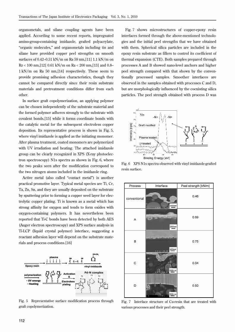
Fig. 7 shows microstructures of copper-epoxy resin
interfaces formed through the above-mentioned technolo-
gies and the initial peel strengths that we have obtained
with them. Spherical silica particles are included in the
epoxy resin substrate as fillers to control its coefficient of
thermal expansion (CTE). Both samples prepared through
processes A and B showed nano-level anchors and higher
peel strength compared with that shown by the conven-
tionally processed samples. Smoother interfaces are
observed in the samples obtained with processes C and D,
but are morphologically influenced by the coexisting silica
particles. The peel strength obtained with process D was
Fig. 5 Representative surface modification process throughgraft copolymerization.
Fig. 6 XPS N1s spectra observed with vinyl imidazole-graftedresin surface.
Fig. 7 Interface structure of Cu-resin that are treated withvarious processes and their peel strength.

113
comparable to that obtained conventionally, whereas that
for process C was inferior to the conventional process.
3. Challenges from the viewpoint of package manu-facturing
Even if adequate adhesion strength of copper layer
formed on a smooth surface is achieved with simple test
samples, various further capabilities are simultaneously
required to realize high-density packaging.
3.1 ReliabilityAmong various methods we examined to promote the
adhesion strength of the copper layer, some of them
showed considerable degradation during one or more of
the reliability tests: TC (temperature cycle), TS (Thermal
shock cycle), HAST (highly accelerated temperature and
humidity stress test), or reflow cycles. The typical failure
mode was peeling off along the copper-resin interface.
Some samples, however, showed an obvious intra-resin
break, and resin fragments were observed on the peeled
copper face. The microstructure of this break mode corre-
sponds to a cohesive break that usually results in higher
peel strength. This poor correlation between the micro-
structure and the actual strength strongly suggests a weak
boundary layer being formed during the process.
3.2 ProcessabilityAlthough adhesion performance was quite durable,
some materials showed poor processability for high-
density wiring. For example, as shown in Fig. 8a, a dry film
resist (DFR) in photolithography became hard to remove,
probably caused partly by the excessively promoted adhe-
sion to the film. By contrast, if the adhesion-promoting
layer has poor affinity to the resist film, washing away or
floating issues could occur, resulting in defocusing and
poor resolution, like the examples shown in Figs. 8b, c,
and d. This affinity relation is a bit complicated. While
stronger adhesion is preferable for the resin-copper,
copper-resin, copper-solder resist, and resin-solder resist
interfaces, adhesion strength should be appropriate (not
too strong or too weak) for resin (or seed layer)-patterning
resist. Since the surface characteristics of silica are differ-
ent than those of most resin types, differences in particle
size distribution and the total content (volume fraction) of
silica included in the resin affect the adhesion properties.
To avoid this, an additional filler-free layer was applied
onto the conventional resin layer including filler, where
the latter layer has a role in controlling TCE and rigidity.
This added layer also provides a highly smooth surface
when modified only chemically. Nevertheless, this hetero-
layer structure sometimes shows difficulty in the laser via
hole forming process due to a difference in their ease of
abrasion, as seen in Fig. 9. There was a case in which an
element included in the promotion layer could not be suf-
ficiently removed, leading to poor connection durability at
the via-bottom (Fig. 10). The interference caused by the
introduced adhesion promoter in the processing should be
analyzed and solved in order to achieve high-density wir-
ing. Although some modification of the existing processes
should be tried for cost-effective solutions, additional pro-
cesses will be needed when the optimum condition is out
of the modification range. For instance, an additional etch-
Fig. 8 Issues relating to material or processing conditionsthat are newly introduced for the adhesion promotion; a. DFRremoval failure, b. floated DFR failure, c. DFR resolution errorand d. missing line.
Fig. 9 Cross sectional view of laser drilled via of a. hetero-laminated layer, and b. conventional single layer includingfiller.
Fig. 10 Residue of a newly applied element on a via-bottom.
Horiuchi et al.: Metallization Technologies on a Smooth Resin Surface (4/6)

114
Transactions of The Japan Institute of Electronics Packaging Vol. 3, No. 1, 2010
ing process to remove the element included in the adhe-
sion promoting layer should be introduced if the analysis
indicates the inability of the existing process to complete
the removal. Fig. 11 demonstrates fine copper lines 4um
wide with 4um spaces formed on conventionally rough-
ened, un-roughened, and additionally stacked-up filler-free
resin layer surfaces.
3.3 PerformanceEven within the same magnitude of roughness, it is
reported that peel strength varies depending on the rough-
ened surface morphology, and pore-type roughness is
superior to a peak-valley structure in respect to mechanical
anchoring.[8] Since such a difference in roughness
morphology may lead to a difference in the relative con-
ductor-resin interface area, its effect on transmission per-
formance, especially S21 at high frequencies, should be
analyzed. Also, even if the surface has a very low roughness
profile or is very smooth, the effects on the transmission
properties of the actual impedance of alloy/intermetallic or
of other adhesion-promoting layers newly introduced
between the resin layer and the conductor metal should be
considered. Dimensional control of transmission lines in
the manufacturing process becomes more important.
3.4 Environmental standpoint and costThe requirements to minimize the environmental bur-
den have become more rigorous. Substances newly
adopted in the manufacturing process need, at least, to sat-
isfy the demands of the existing legislation or rules
restricting the use of hazardous substances, such as RoHS
(Restriction of the use of certain Hazardous Substances in
electrical and electronic equipments) and REACH (Regis-
tration, Evaluation, Authorization and Restriction of Chem-
icals). Additionally, substances that impact on climate
should be avoided. For instance, fluorocarbons that are
broadly used as etching gases have extremely high global
warming potentials (GWPs). Fig. 12 compares GWPs and
safety levels given with NFPA (National Fire Protection
Association) standards among various fluorocarbons. In
spite of its high chemical stability and bio-inertness, CF4
has a very high GWP of 6500, so that its thorough decom-
position is necessary. Taking these actions is possible and
the corresponding equipment is commercially available,
but the question here is its cost-effectiveness. Similar con-
sideration will be needed for performance-cost balance.
For instance, although Ti can be an efficient adhesion pro-
moter on a smooth surface, it cannot be removed by typi-
cal etchants for seed copper removal, so that an additional
etch bath containing a different etchant such as HF will be
needed. In a case like this, some other cost reductions in
another part of the manufacturing process will be strongly
desired to compensate for the additional process cost.
4. ConclusionSome methods providing sufficient copper peel strength
on smooth surface have become available. To apply them
to the next generation of packaging practically, however,
various process improvements and optimizing are still
needed.
References
[1] ITRS, http://www.itrs.net/Links/2007ITRS/2007_
Chapters/2007_Assembly.pdf
[2] S. H. Hall, et al., “High-speed digital system design,”
pp. 74–87, John-Wiley & Sons, New York, 2000.
[3] A. Deutsch, et al., “Prediction of Losses Caused by
Roughness of Metallization in Printed-Circuit
Boards,” IEEE Trans. Adv. Packag., Vol. 30, pp.
279–287, 2007.
[4] Y-B. Park, et al., “Effect of Wet Chemical Pretreat-
ment Conditions on the Interfacial Adhesion Energy
between Electroless-Plated Ni and Polyimide
Films,” JJAP, 48, 08HL03, 2009.
[5] M. Sugimoto, et al., “Adhesion mechanism of plating
Fig. 11 4 μm-lines/4 μm-spaces formed on a. conventionallyroughened, b. un-roughened, and c. additionally stacked-upfiller-free resin layer surfaces.
Fig. 12 Global warming potential (GWP) and safety level(NFPA704) of various gases.
115
on surface reformed resin by UV irradiation,”
Hyoumenngijutsu (Surface Technology), Vol. 59,
pp. 294–298, 2008, in Japanese.
[6] K. Inoue, et al., “Surface modification of polyimide
using UV light and formation of circuit patterns,”
Hyoumengijutsu (Surface Technology), Vol. 59, pp.
47–50, 2008.
[7] D. Bhusari, et al., “Plasma treatment and surface
analysis of polyimide films for electroless copper
buildup process”, J. Electrochem. Soc., Vol. 152,
pp. F162–F170, 2005.
[8] H. Hayden, et al., “Adhesion Enhancement Between
Electroless Copper and Epoxy-based Dielectrics,”
IEEE Trans. Adv. Packag., Vol. 32, pp. 758–767,
2009.
[9] S. Fukutani, et al., “Surface modification of a crystal-
line polymer film using 172 nm vacuum ultraviolet
light for fabricating copper fine pattern,” J. Jap. Inst.
Electro. Pack., Vol. 8, pp. 325–329, 2005, in Japanese.
[10] M.Watanabe, et al., “Surface modification of liquid
crystal polymers using UV irradiation,” J. Jap. Inst.
Electro. Pack., Vol. 11, pp. 152–156, 2008, in
Japanese.
[11] K. Hontake, et al., “Copper Plating Method on Flat
Surface for High Frequency Signal Transfer,” JJAP,
Vol. 44, pp. 6719–6725, 2005.
[12] K. Kawamura et al., “Surface Graft Polymer Inter-
layer as a Means of Improving Adhesion of Copper
for Fine-pitch Printed Wiring Boards,” pp. 51–54,
FUJIFILM RESEARCH & DEVELOPMENT (No.52-
2007), in Japanese.
[13] S. Z. Shi, et al., “Molecular Modification of PCB Sub-
strates: Demonstration of HAST Survivability of
Fine-Line Patterned Structures,” ICEP, 2009.
[14] P. Brooks, et al., “Novel approach for a non-etching
adhesion promoter for the next generation of IC
substrates,” Atotech, Circuitree, June, 2007.
[15] G. H. Yang, et al., “Electroless deposition of copper
on polyimide films modified by surface graft copoly-
merization with nitrogen-containing vinyl mono-
mers,” Colloid Polym. Sci., Vol. 279, pp. 745–753,
2001.
[16] R. N. Dean, et al., “Realization of ultra fine pitch
traces on LCP substrates,” IEEE Trans. Comp.
Pack. Technol., Vol. 31, pp. 315–321, 2008.
Horiuchi et al.: Metallization Technologies on a Smooth Resin Surface (6/6)


