Introducing ePMA into a Paediatric ITU Will Hall - Lead Pharmacist for ePMA.

Association of Metallurgical Engineers of Serbia AMES
Scientific paper UDC: 669.018:681.723.2
METALLIC MATERIALS-APPLICATION OF TEM, EPMA AND SEM IN SCIENCE AND ENGINEERING PRACTICE
Milan T. Jovanović *, Nenad Ilić, Ilija Bobić, Ivana Cvijović-Alagić, Višeslava Rajković, Zoran Mišković
Institute of Nuclear Sciences “Vinča”, P.O. Box 522, 11001 Belgrade, Serbia
Received 20.12.2009 Accepted 30.12.2009.
Abstract Examples of application of transmission electron microscope (TEM), electron probe X-ray microanalyzer (EPMA) and scanning electron microscope (SEM) in microstructural investigation of metallic materials are described. All investigations have been carried out at the Department of Materials Science, Institute of Nuclear Sciences, Vinča, Serbia. Key words: metallic materials, TEM, EPMA, SEM, microstructure, science, practice
Introduction Although the activities at the Department of Materials Science cover the research
and development of a wide range of materials such as metals and alloys, ceramics and carbon materials, the scope of this paper will be exclusively focused on investigation of metallic materials.
The paper actually represents a historical review of application of transmission electron microscope (TEM), electron probe X-ray microanalyzer (EPMA) and scanning electron microscope (SEM) in microstructural investigation of different metals and alloys. These activities were not only connected with scientific research and development, but were also aimed to engineering practice and forensic studies.
TEM “JEOL-JEM 7A” was operating between 50 and 100 KeV depending on investigated materials and the technique applied for the sample preparation (thin foil or replica).
Data acquired by EPMA “Cambridge Instruments” were complementary to those obtained by TEM enabling qualitative and quantitative analysis of present phases and inclusions.
* Corresponding author: Milan T. Jovanović [email protected]
258 MJoM Vol 15 (4) 2009 p. 257-266
SEM “Philips XL30” with addition of an energy dispersive spectroscope (EDS) served not only for observation of microstructure and fracture topography, but also for qualitative and quantitative analysis.
However, due to aging and absence of outdated spare parts most of these valuable instruments are not in the working condition.
Results and Discussion
TEM investigations Samples for TEM were mostly thin foils which were prepared by the “double jet
technique”. The object of investigations were ferrous and non-ferrous metals and alloys including, among others, Cu and Al-based alloys and alloys based on precious metals. Some examples of these investigations will be demonstrated in the following text.
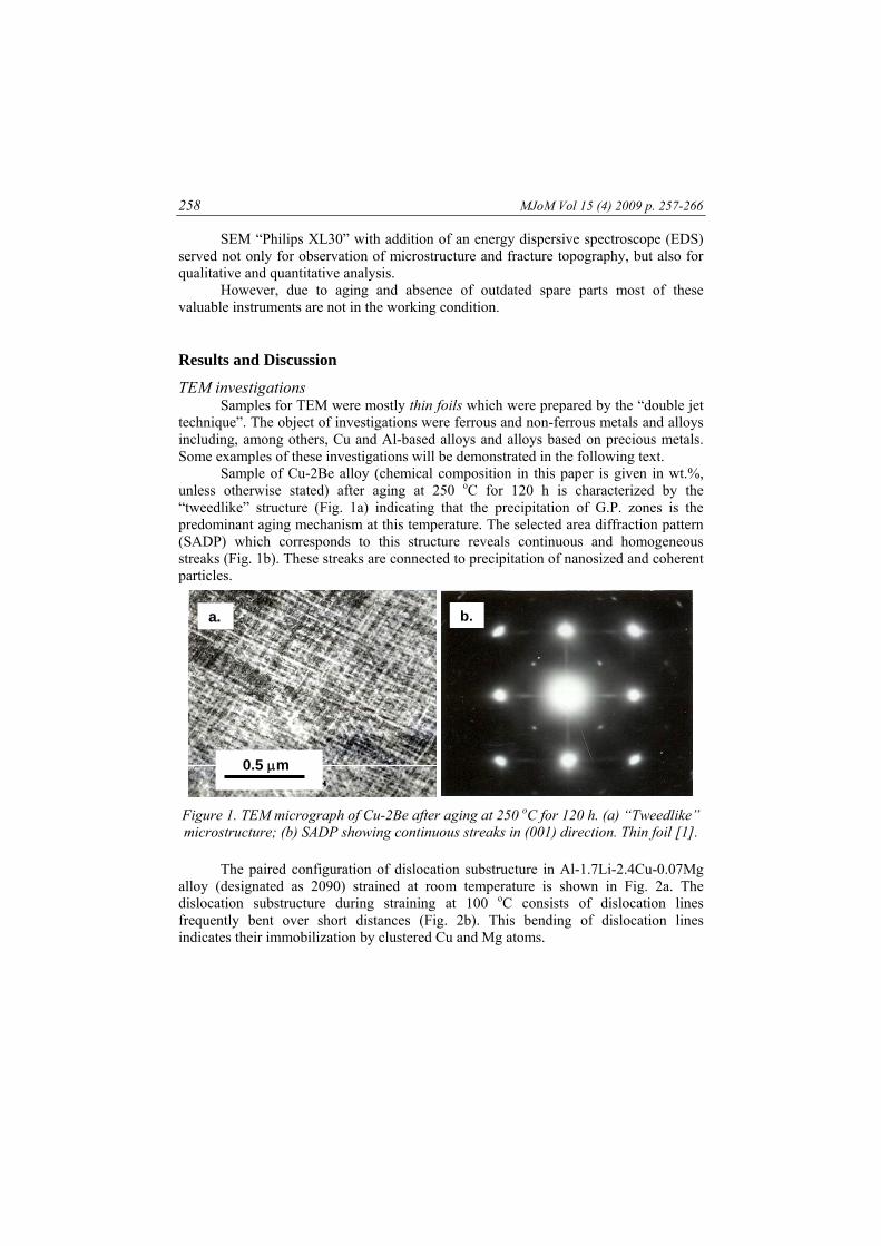
Sample of Cu-2Be alloy (chemical composition in this paper is given in wt.%, unless otherwise stated) after aging at 250 oC for 120 h is characterized by the “tweedlike” structure (Fig. 1a) indicating that the precipitation of G.P. zones is the predominant aging mechanism at this temperature. The selected area diffraction pattern (SADP) which corresponds to this structure reveals continuous and homogeneous streaks (Fig. 1b). These streaks are connected to precipitation of nanosized and coherent particles.
0.5 μm
a.
b.
Figure 1. TEM micrograph of Cu-2Be after aging at 250 oC for 120 h. (a) “Tweedlike” microstructure; (b) SADP showing continuous streaks in (001) direction. Thin foil [1].
The paired configuration of dislocation substructure in Al-1.7Li-2.4Cu-0.07Mg
alloy (designated as 2090) strained at room temperature is shown in Fig. 2a. The dislocation substructure during straining at 100 oC consists of dislocation lines frequently bent over short distances (Fig. 2b). This bending of dislocation lines indicates their immobilization by clustered Cu and Mg atoms.
Jovanović et al- Metallic materials-application of TEM, EPMA and SEM... 259
0.2 μm
a.
0.2 μm
b.
Figure 2. TEM micrograph of Al-1.7Li-2.4Cu-0.01Mg alloy. (a) Dislocation
substructure after room-temperature straining (5%) showing dislocation pairs; (b) substructure after straining (5%) at 100 oC showing “aged” dislocations (denoted with arrows) as an indication of dislocation reaction with clustered Cu and Mg atoms. Thin
foil [2] On many occasions the replica technique was applied in order to obtain an
adequate sample to study morphology of present phases by TEM. The effect of heat treatment on the microstructure of Ni and Co-based
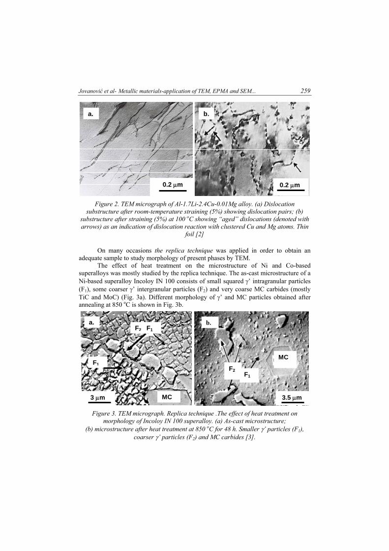
superalloys was mostly studied by the replica technique. The as-cast microstructure of a Ni-based superalloy Incoloy IN 100 consists of small squared γ’ intragranular particles (F1), some coarser γ’ intergranular particles (F2) and very coarse MC carbides (mostly TiC and MoC) (Fig. 3a). Different morphology of γ’ and MC particles obtained after annealing at 850 oC is shown in Fig. 3b.
a.
3 μm
F1
F2
MC
F1
3.5 μm
MC
F2
b.
F1
Figure 3. TEM micrograph. Replica technique .The effect of heat treatment on
morphology of Incoloy IN 100 superalloy. (a) As-cast microstructure; (b) microstructure after heat treatment at 850 oC for 48 h. Smaller γ’ particles (F1),
coarser γ’ particles (F2) and MC carbides [3].

260 MJoM Vol 15 (4) 2009 p. 257-266
On the example of Ag-11Au-20Pd-2Pt-13.5Cu-1.5Zn dental alloy the application of EPMA on characterization of phases is illustrated in Fig. 4. The electron image (Fig. 4a) shows that F1 and F2 plate-like phases appear in the microstructure. X-ray micrographs shown in Fig 4(b-e) illustrate the distribution of alloying elements, while Fig. 4g, h represents the distribution of elements along the scanning line L (in Fig. 4a). A semiquantitative analysis of F1 and F2 phases is shown in Table 1.
F1
F2
L
a. b. c. d.
e. f.
g. h.
Figure 4. EPMA micrograph of Ag-11Au-20Pd-2Pt-13.5Cu-1.5Zn alloy. (a) Electron
image; (b) Zn distribution; (c) Pd distribution; (d) Cu distribution; (e) Ag distribution; (f) Pt distribution; (g) Cu+Pd distribution along line L; (h) Ag+Pt distribution along
line L [4].
Table 1 Distribution of major chemical elements in F1 and F2 phases. Element, wt.% Phase Cu Pd Zn Au Pt Ag
F1 22 42 13 5.5 7 5 F2 45 20 2.5 10 3 12 These results imply that the amount of Zn and Pd was higher in the F1 phase, but
the concentration of Cu was higher in the F2 phase. In both phases the amount of Ag was much lower than in the surrounding matrix, whereas Pt and Au were rather uniformly distributed throughout the matrix. These results clearly show that F1and F2 phases may be regarded as PdZn-rich and CuPd-rich phases, respectively.
Fig. 5 represents the distribution of elements in as-cast superalloy Pratt& Whitney (PR 444). The highest amount of Ti was detected in the multiple grain boundary, whereas W and Cr were at their minima.
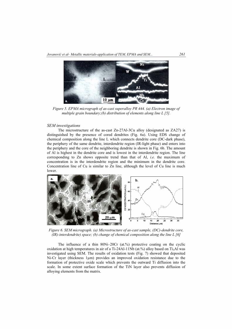
Jovanović et al- Metallic materials-application of TEM, EPMA and SEM... 261
Figure 5. EPMA micrograph of as-cast superalloy PR 444. (a) Electron image of
multiple grain boundary;(b) distribution of elements along line L [5].
SEM investigations The microstructure of the as-cast Zn-27Al-3Cu alloy (designated as ZA27) is
distinguished by the presence of cored dendrites (Fig. 6a). Using EDS change of chemical composition along the line L which connects dendrite core (DC-dark phase), the periphery of the same dendrite, interdendrite region (IR-light phase) and enters into the periphery and the core of the neighboring dendrite is shown in Fig. 6b. The amount of Al is highest in the dendrite core and is lowest in the interdendrite region. The line corresponding to Zn shows opposite trend than that of Al, i.e. the maximum of concentration is in the interdendrite region and the minimum in the dendrite core. Concentration line of Cu is similar to Zn line, although the level of Cu line is much lower.
b.
20 μm DC
IR
a.
Figure 6. SEM micrograph. (a) Microstructure of as-cast sample, (DC)-dendrite core,
(IR)-interdendrite) space; (b) change of chemical composition along the line L [6] The influence of a thin 80Ni–20Cr (at.%) protective coating on the cyclic
oxidation at high temperatures in air of a Ti-24Al-11Nb (at.%) alloy based on Ti3Al was investigated using SEM. The results of oxidation tests (Fig. 7) showed that deposited Ni-Cr layer (thickness 1µm) provides an improved oxidation resistance due to the formation of protective oxide scale which prevents the outward Ti diffusion into the scale. In some extent surface formation of the TiN layer also prevents diffusion of alloying elements from the matrix.

262 MJoM Vol 15 (4) 2009 p. 257-266
Figure 7. SEM micrograph. Ti-24Al-11Nb alloy annealed in air at 600 oC for 120 h. (a)
With Ni-Cr protection layer; (b) without protection; (c) fractured oxide layer [7] SEM is a powerful tool for investigation of mechanism of fracture. One of the
numerous projects of this kind was investigation of effect of heat treatment (HT) on the welded steel rail joints (Fig. 8).
b.a.
c. d.
Figure 8. SEM micrograph. (a) Microstructure of the as-welded joint in the NHT
condition; (b) fracture surface of the welded joint in the NHT condition; (c) microstructure of HT weld; (d) fracture surface of the welded joint in the HT
condition [8] It was found that HT improves the mechanical properties of joints and changes
the fracture mechanism from brittle to ductile. Coarse islands of pearlite in the non-heat treated (NHT) weld joint (Fig. 8a) induce brittle fracture which occurred after a small
a. b. c.
Jovanović et al- Metallic materials-application of TEM, EPMA and SEM... 263
plastic deformation (1.5%). Higher magnification disclosed blocks of low-energy cubic planes along which cleavage occurred causing brittle fracture (Fig. 8b). By contrast, in the HT condition improved strength and elongation are attributed to the finer ferrite-pearlite microstructure (Fig. 8c) and the different fracture mechanism. The rupture occurred after larger plastic deformation (7%), i.e. ductile fracture was the operating fracture mechanism distinguished by microvoid coalescence and the creation of ductile dimples on the fracture surface (Fig. 8d).
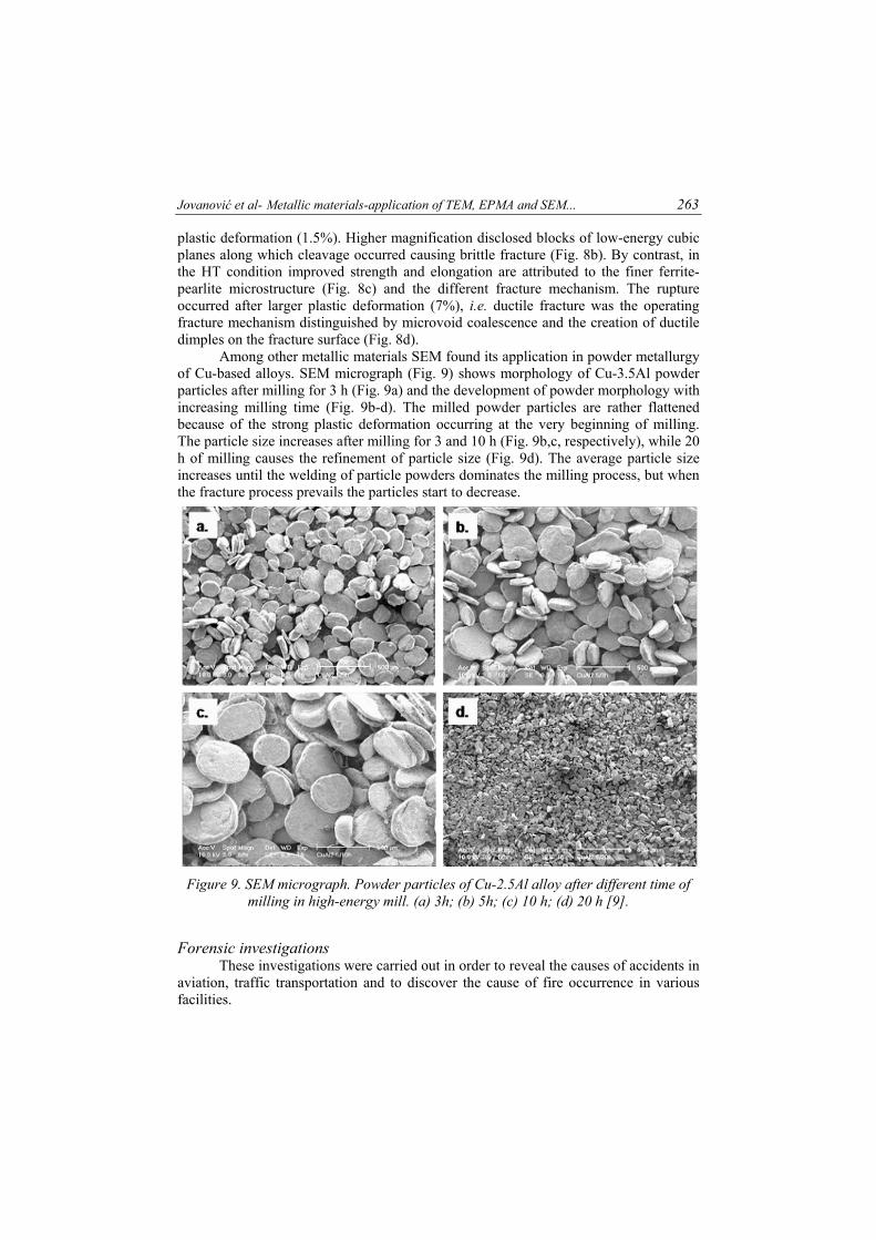
Among other metallic materials SEM found its application in powder metallurgy of Cu-based alloys. SEM micrograph (Fig. 9) shows morphology of Cu-3.5Al powder particles after milling for 3 h (Fig. 9a) and the development of powder morphology with increasing milling time (Fig. 9b-d). The milled powder particles are rather flattened because of the strong plastic deformation occurring at the very beginning of milling. The particle size increases after milling for 3 and 10 h (Fig. 9b,c, respectively), while 20 h of milling causes the refinement of particle size (Fig. 9d). The average particle size increases until the welding of particle powders dominates the milling process, but when the fracture process prevails the particles start to decrease.
Figure 9. SEM micrograph. Powder particles of Cu-2.5Al alloy after different time of
milling in high-energy mill. (a) 3h; (b) 5h; (c) 10 h; (d) 20 h [9].
Forensic investigations These investigations were carried out in order to reveal the causes of accidents in
aviation, traffic transportation and to discover the cause of fire occurrence in various facilities.
264 MJoM Vol 15 (4) 2009 p. 257-266
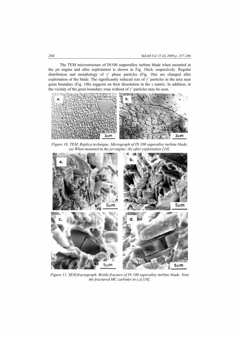
The TEM microstructure of IN100 supperalloy turbine blade when mounted in the jet engine and after exploitation is shown in Fig. 10a,b, respectively. Regular distribution and morphology of γ’ phase particles (Fig. 10a) are changed after exploitation of the blade. The significantly reduced size of γ’ particles in the area near grain boundary (Fig. 10b) suggests on their dissolution in the γ matrix. In addition, in the vicinity of the grain boundary zone without of γ’ particles may be seen.
a. b.
Figure 10. TEM. Replica technique. Micrograph of IN 100 superalloy turbine blade.
(a) When mounted in the jet engine; (b) after exploitation [10].
a. b.
c. d.
Figure 11. SEM fractograph. Brittle fracture of IN 100 superalloy turbine blade. Note
the fractured MC carbides in c,d [10].
Jovanović et al- Metallic materials-application of TEM, EPMA and SEM... 265
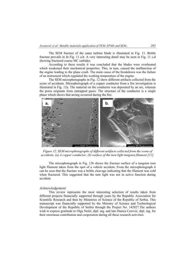
The SEM fracture of the same turbine blade is illustrated in Fig. 11. Brittle fracture prevails in In Fig. 11 a,b. A very interesting detail may be seen in Fig. 11 c,d showing fractured coarse MC carbides.
According to these results it was concluded that the blades were overheated which weakened their mechanical properties. This, in turn, caused the malfunction of the engine leading to the plane crash. The main cause of the breakdown was the failure of an instrument which regulated the working temperature of the engine.
The SEM microphotographs in Fig. 12 show different artifacts collected from the scene of accidents. Microphotograph of a copper conductor from a fire investigation is illustrated in Fig. 12a. The material on the conductor was deposited by an arc, whereas the pores originate from entrapped gases. The structure of the conductor is a single phase which shows that arcing occurred during the fire.
a.
b.b.
Figure 12. SEM microphotographs of different artifacts collected from the scene of
accidents. (a) A copper conductor; (b) surface of the turn light tungsten filament [11]. The microphotograph in Fig. 12b shows the fracture surface of a tungsten turn
light filament taken from the spot of a vehicle accident. From the microphotograph it can be seen that the fracture was a brittle cleavage indicating that the filament was cold when fractured. This suggested that the turn light was not in active function during accident.
Acknowledgement This review represents the most interesting selection of results taken from
different projects financially supported through years by the Republic Association for Scientific Research and then by Ministries of Science of the Republic of Serbia. This manuscript was financially supported by the Ministry of Science and Technological Development of the Republic of Serbia through the Project No. 142027.The authors wish to express gratitude to Olga Nešić, dipl. ing. and late Danica Cerović, dipl. ing. for their enormous contribution and cooperation during all these research activities.
266 MJoM Vol 15 (4) 2009 p. 257-266
References
[1] Đ. Drobnjak, M. Jovanović, B. Đurić, Met. Sci. 11 (1977) 196-199. [2] N. Ilić, M.T. Jovanović, V. Radmilović, Đ. Drobnjak, Int. J.Mat. Res. 12 (2005)
1386-1390. [3] Milan T. Jovanović, Borislav Lukić, Zoran Mišković, Ilija Bobić, Ivana
Cvijović, Biljana Dimčić, Metalurgija, 13 (2007) 91 – 106. [4] D. Cerović, S. Stanković, B. Đurić, M. Jovanović, Metallography 18 (1985) 395. [5] Z Mišković, B Lukić, M Gligić, M Jovanović, Vacuum 40 (1990) 125-129. [6] I. Bobić, M. T. Jovanović, N. Ilić. Mat. Letters 57 (2003), 1683-1688. [7] I. Cvijović, M.T. Jovanović, D. Peruško. Corr. Sci. 50 (2008) 1919–1925. [8] Nenad Ilić , Milan T. Jovanović , Miša Todorović, Milan Trtanj, Petar Šaponjić.
Mat. Charact. 43 (1999) 243-250. [9] Višeslava Rajković, D. Božić, Serbian Society for Microscopy, 50 Years of
Electronic Microscopy in Serbia, Belgrade 2006, p. 116. [10] B. Lukić, M.T. Jovanović, XXIV October Symposium of Mining and
Metallurgical Engineers of Serbia, Donji Milanovac 1992, p. 400, in Serb. [11] Z. Mišković, Internal report, in Serb.