MEMS Spatial Light Modulator for Holographic Displays
69
MEMS Spatial Light Modulator for Holographic Displays Elroy L Pearson B.S.E.C.E, USU, 1999 A.S.E.E., Ricks College, 1996 Submitted to the Program in Media Arts and Sciences, School of Architecture and Planning, In Partial Fulfillment of the Requirements for the Degree of MASSACHUSETTS INgTITUTE- OF TECHNOLOGY Master of Science ~o~jMAR 0420 September 2001 @Massachusetts Institute of Technology, 2001. LIBRARIES All Rights Reserved Author_ (5 Program in Media Arts and Sciences Certified by Stephen A. Benton E. Rudge ('48) and Nancy Allen Professor of Media Arts and Sciences, MIT Media Laboratory Accepted by_.. Dr. Andrew B. Lippman Chair, Departmental Committee on Graduate Students Program in Media Arts and Sciences
Transcript of MEMS Spatial Light Modulator for Holographic Displays

MEMS Spatial Light Modulator forHolographic Displays
Elroy L PearsonB.S.E.C.E, USU, 1999
A.S.E.E., Ricks College, 1996
Submitted to the Program in Media Arts and Sciences,School of Architecture and Planning,
In Partial Fulfillment of the Requirements for the Degree of MASSACHUSETTS INgTITUTE-OF TECHNOLOGY
Master of Science~o~jMAR 0420
September 2001@Massachusetts Institute of Technology, 2001. LIBRARIES
All Rights Reserved
Author_
(5 Program in Media Arts and Sciences
Certified byStephen A. Benton
E. Rudge ('48) and Nancy Allen Professor ofMedia Arts and Sciences, MIT Media Laboratory
Accepted by_..Dr. Andrew B. Lippman
Chair, Departmental Committee on Graduate StudentsProgram in Media Arts and Sciences

2

MEMS Spatial Light Modulator for HolographicDisplays
Elroy L. Pearson
Submitted to the Program in Media Arts and Sciences,School of Architecture and Planning,in Partial Fulfillment of the Requirements for the Degree ofMaster of Science
Abstract
This thesis presents new approaches to building holographicdisplays. The approaches use a diffractive spatial light modulator(SLM) built using microelectromechanical system (MEMS)technology. Several related MEMS SLMs are reviewed. Inparticular, the capabilities of Silicon Light Machines' Grating LightValve (GLV T) and the Polychromator by Honeywell, Sandia, andMIT are examined because they are both diffractive SLMs. Aholographic display design is presented that is based on adiffractive SLM that combines the spatial resolution of the GLVwith the addressability of the Polychromator. The holographicdisplay system design and the MEMS fabrication process aredescribed. Although the MEMS device was not fully fabricated,much of the process was developed. The successful process stepsand suggestions for process improvements are laid out. Finally animproved MEMS SLM process and a scalable MEMS holographicdisplay are proposed.

4

MEMS Spatial Light Modulator for HolographicDisplays
Elroy L. Pearson
Kr Stephen A. BentonE. Rudge ('48) and Nancy Allen Professor of
Media Arts and Sciences, MIT Media Laboratory
Scott ManalisProfessor of Media Arts and Sciences
MIT Media Laboratory
Pierre St-HilaireResearch Scientist
Templex Corp.

6

7

8

AcknowledgementsMore people have helped make this thesis possible than can adequatelybe addressed here. Another thesis could probably be written on thattopic alone. I would like to thank all of those who contributed in oneway or another to this effort.
In particular I would like to thank Shelly for her unconditional supportand love. I am not whole without you. My children Kaili, Louis, andLeRoyce have been the spice of my life. There is nothing like havingthem all run up and jump into my arms for a hug.
Stephen Benton has been an inspiration and guide. He has supportedeven my craziest ideas and corrected my errors.
Scott Manalis has introduced me to a whole new world ofmicrofabrication. What fun!
Thanks to the MEMS fabrication team from the fall 2000 class. DianaYoung, Yael Macguire, James White, Matt Reynolds, and Guy Rasmuthcombined some incredible skills to design a great project.
Many thanks go to Aditya Prabhakar, Aaron Weber, and Wendy Plesniak- the other grad students in the group. Aditya endured many sleeplessnights of thesis writing with me and helped keep me sane. Aaron is anamazing optical engineer and more often than not a great cook. Wendyis a talented engineer, scientist, and artist - a rare find. Her timelyadvice has helped me keep everything in perspective. Thanks to Ollie forproofreading my thesis and making me formulate my thoughts moreclearly.
Thanks to Steve Smith and Thomas Nwodoh. Steve has terrific practicalexperience to go with his scientific understanding. I would like to thankhim for letting me build his shed with him. Thanks for the hammer. Ithas been fun to compare stories about the kids with Tom and Steve.
I have much appreciation for the many talented UROPs that havecontributed to group. I have always been able to count on Daniel, Rob,Julie, Altay, and the others to lighten my spirits and ask really goodquestions. Thanks to Daniel for being a good friend that I can talk to formuch too long.

Thanks to the previous SPIers for inspiration and advice. Pierre St-Hilaire continues to amaze me with his technical prowess and scientificunderstanding. Bill and Julie Parker been friends since we met them twoyears ago. I look forward to working with you.
Thanks to the faculty and staff at MTL. In particular Paul Tierney hasbeen a great support.
Thanks to Richard Rallison for giving me my first real introduction toholography and research. I learned laser safety from the guy that talkedme into jumping from a cherry picker over a pool attached to a bungeecord.
I would like to thank Mom and my brothers and sisters for helping meget to where I am today. Mom taught me to really think about things andnot take anything for granted.
Finally I would like to thank Dad for teaching me the value of integrityand hard work and the importance of family. You'll never see megraduate from college - on this Earth. Thanks for watching from theother side.

11
ContentsABSTRA CT ................................................................................................... 3
ACKNOWLEDGEMENTS..........................................................................9
1. INTRODUCTION .................................................................................... 13
1.1 MOTIVATION .................................................... 13
1.1.1 History of Image Production...............................................131.1.2 The Human Visual System........................................................... 141.1.3 Three-dimensional Displays ........................... 151.1.4 The Acousto-optic Spatial Light Modulator................................161.1.5. MEMS-based SLMs................................ 18
1.2 CONTENT OF THESIS ........................................................................ 18
2. SPATIAL LIGHT MODULATORS......................................................21
2.1 STRUCTURE AND OPERATION OF THREE MEMS SLMs ....................... 212.1.1 Texas Instruments' DMDTM. .................................. 212.1.2 Diffractive SLMS..............................222.1.3 Silicon Light M achines' GLV ...................................................... 222.1.3 The Polychromator ................................. 24
2.2 SLM COMPARISONS ............................................. 25
2.2.1 Diffraction Efficiency ......................................... ..... 252.2.2 Bandwidth.......................................25
2.3 FEASIBILITY OF HOLOGRAPHIC DISPLAYS BASED ON THESE MEMS-SLMs
....................................................................................................................... 2 7
3. SYSTEM DESIGN ....................................................................................... 29
3.1 SLM DESIGN . ........................................... ....... 29
3.1.1 SLM Mechanical and Electrical Design ................... 293.1.2 SLM P inout ................................................................................. 353.1.3 SLM Microfabrication Process Design...................373.1.3 SLM Optical Analysis............. .................. 433.2 Optical Architecture Design .......................................................... 46
3.3 SUMMARY ........................................................ .............. 49
4. PROCESSING ........................................................................................ 51
4.1 PROCESS OVERVIEW..................... ............................... 51
4.1.1 Chapter Contents .................................. 514.2 THIN FILM APPLICATION ........................................ 51
4.2.1 Thermal Oxide Growth .... .......................................... 514.2.2 Polysilicon Deposition................................................................. 524.2.3 Nitride D eposition.............. .................................. 53
4.3 LITHOGRAPHY ...................................................... 54
4.3.1 Photoresist ....................... ................ 54
12
4.3.2 Stepper................................... 544.4 PLASM A ETCHING ................................................................................ 55
4.4.1 Nitride Etch ............................................... 554.4.2 Oxide Etch ..... .......... ............................ 554.4.3 Polysilicon Etch............................. ...... 554.5.1 KOH Etch of Polysilicon ................ .................. 564.5.2 Stepper Lithography for Liftoff..................................................... 574.5.3 Metal Deposition for Electrodes and Traces................................ 574.5.4 M etal Liftofffor Traces ............................................................... 57
4.6 R ELEASE ETCH..................................................................................... 584.6.1 Release Etch ............. ............................... ....... 58
4.7 P ACKAG IN G .......................................................................................... 584.7.1 Packaging....................................... 58
4.7 CONCLUSION. .............................................. 59
5. CONCLUSIONS AND SUGGESTIONS FOR FUTURE WORK ......... 61
5 .1 R EV IEW ................................................................................................. 6 15.1.1 Thesis R eview ............................................................................... 61
5.2 SUGGESTIONS FOR FUTURE WORK..................................... 615.2.1 SLM Fabrication ............................................................................. 61
5.3 C ONCLUSION S....................................................................................... 675.3.1 Conclusions ................................ 67
REFERENCES............................................................................................. 68

1. Introduction
1.1 Motivation
1.1.1 History of Image ProductionFor millennia people have imagined illusions so realistic that the viewerwould not be able to determine whether the observed scene is real orfabricated. At first, it was likely assumed that the most probable way tocreate such an illusion would be through magic. The first realizations ofconvincing images were probably achieved though art forms such assculpture and painting. Artists such as Michelangelo created amazinglikenesses of people and other subjects using these media.Michelangelo's ability to recreate accurate details went virtuallyunmatched for centuries.
Figure 1.1 Michelangelo's David (left) and Sistine Chapel fresco (detail of "TheCreation of Adam" at right) demonstrate the amazing realism that Michelangeloachieved through sculpture and painting.
During the last few hundred years, technology advanced enough toenable great breakthroughs in recording and displaying our visual world.Still cameras enabled us to record moments in incredible detail. Movieshave let us capture and replay the complexity of movement. Thesemedia changed the way we communicated visually and empowered thosewho wielded them masterfully.
The closer our visual communications come to matching the abilities ofthe human visual system, the more our potential for communicating

expands. The paintings and pictures are able to show two-dimensionalimages. Sculptures are able to replicate the three-dimensionality of ascene. Movies are able to make two-dimensional images move.However, none of these media alone are capable of reproducing all of thevisual cues that most humans are able to see. Conspicuously lacking inthe tool set of visual communications is the ability to generate three-dimensional moving pictures.
1.1.2 The Human Visual SystemPeople have invented various approaches to creating three-dimensionalmoving images. The great majority of these efforts have used techniquesto send different images to each eye to take advantage of stereopsis.
Stereopsis is the ability to discern depth through the slightly differingimages that each eye sees because they are physically located a shortdistance from each other. The brain interprets the differences in theseimages along with other depth cues to determine the depth of objects in ascene. Using color or polarization filtering glasses or head-mounteddisplays can produce stereo vision. However, stereopsis is only onedepth cue among many that are important to three-dimensional imaging.
Most humans actually combine many visual cues to see depth in scenes.These cues include stereopsis, occlusion, ocular accommodation,shading, convergence, and motion parallax. Motion parallax comes fromseeing new perspectives of a scene as the viewer's head (and thus eyes)move relative to the scene. Ocular accommodation is the ability of theeyes to focus at different depths. Accommodation is a monocular cue, orone that can be seen by using a single eye. This can be observed bylooking through a window at a distant object. As the eye focuses on theobject the window will seem mostly transparent (even if it is fairly dirty).Then, when the eye focuses on the surface of the window, the distantobject will blur out and mostly disappear from the viewer's vision.Convergence is the effect of one's eyes turning slightly inward to view anobject at close range. Occlusion is the disappearance of a distant objectas it passes behind an opaque near object. Most modern displays (as ofthe writing of this thesis) do not attempt to provide binocular cues, butare able to convey the concept of depth fairly well through the use ofpictorial and motion cues (not from the viewer moving but from movingcameras) cues. A good three-dimensional display will make use of notonly these cues, but binocular cues as well.

1.1.3 Three-dimensional DisplaysMost attempts at three-dimensional displays have used primarilystereopsis, convergence, and two-dimensional depth cues to displaydepth at the expense of accommodation. The result is that many peopleget headaches after viewing these displays for even short periods of time.This problem can be kept to a minimum if measures are taken not tomake convergence-accommodation conflicts too great.
Holographic displays promise to deliver all of the depth cues needed tomake truly three-dimensional moving images. Notable holographicdisplays that have been built to date include several holographic videodisplays built in the MIT Media Lab by the Spatial Imaging Group, adisplay built in Japan, and a holographic display built by DERA inEngland.
The MIT 1 2 and Japanese displays are based on a Scophony-style scannedspatial light modulator (SLM) approach. A Scophony system using ascanned SLM was used in a large screen TV in 19393,4. The generallayout of a Scophony-style holographic display is shown in figure 1.2. Inthese systems, the light is modulated as it passes through a crystal SLM.The crystal modulates the light as sound waves are induced by apiezoelectric transducer to travel through the crystal. As these wavespass through the crystal, the crystalline structure is microscopicallystretched and compressed to create areas of increased and decreasedindex of refraction. Light passes through the areas of increased index
Stationary SLM Scanning MirrorMoving Fringes Plane
Lenses*Output Plane AMC
Moving SLM ImageStationary Fringes
Figure 1.2 Scophony-style Scanned SLMHolographic Display

slower than in other areas. This induces a phase delay into the light inthat area.
The DERA system5 uses a combination of SLMs to make holographicimages. Light is projected from an electrically addressable spatial lightmodulator (EASLM) onto a larger optically addressable spatial lightmodulator (OASLM). Though the two styles of display are verydifferent, SLMs are at the heart of both. This thesis focuses primarily onthe SLM used in the Scophony-style holographic display.
1.1.4 The Acousto-optic Spatial Light ModulatorThe capabilities of the SLM determine in large part the ability of thedisplay to show three-dimensional images. The speed at which the SLMcan be updated is important. Its modulation efficiency and the maximumspatial frequency are also key attributes. The smaller the area that anSLM can address the larger an angle it can diffract light. If themodulation area is small enough, significant diffraction effects can beobserved. The resulting angle of diffraction can be determined directlyfrom the grating equation:
X fm = sin(Oil) - sin( 0 t) 1.1
where A is the wavelength of light measured in meters, f, is themaximum spatial frequency measured in meters-1, Oi, is the angle thelight is incident to the modulating medium with respect its normal, and6., is the angle that light leaves the medium. From this relation itbecomes obvious that for an SLM to diffract light at higher angles, itmust be able to address higher spatial frequencies.
An AOM must be driven with higher frequency acoustic waves if higherspatial frequencies are to be achieved. The current MIT holographicvideo display uses acoustic frequencies up to 100 MHz to produce spatialfrequencies up to 81 line pairs per mm. (See the Calculation of spatialfrequency and fringe wavelength in AOMs below.) This enables amaximum deflection of light of 2.9 degrees. This is a much smallerangle than is practical to use.
A holographic display needs to have a viewing angle at least wideenough to permit a viewer to fit both eyes into the view zone at areasonable viewing distance. The view zone should be wide enough to

allow the user to also move his or her head side to side. For a viewingdistance of 600 mm, given that the average human interpupilary distanceis 65 mm, the minimum view angle needs to be 6.2 degrees. Theholographic image can be greatly improved by increasing this angle to 30degrees. This widening of the view angle allows the viewer to move sideto side and observe motion parallax. The deflection angle of the SLMmust be magnified by a series of lenses for this to happen.
Each component that is added to the display increases the complexity ofthe design. The design must be carefully balanced so as not tounnecessarily limit the bandwidth by a poorly chosen part. In the style ofdisplay that MIT uses, the speed of the horizontal scan mirror is dictatedby the speed of sound in the crystal and the distance between the scannerand the AOM. The sound velocity and the drive frequency of theacoustic transducer determine the maximum spatial frequency and,hence, the maximum diffraction angle the AOM can produce. This anglein turn sets one half of the demagnification specification with the viewzone requirement setting the other half. In fact, setting the specificationsfor a holographic display is a bit like smoothing wallpaper - when youfix one area a bubble pops up in another. All of the components areintimately linked.
Calculation of spatial frequency and fringe wavelength in AOMsThe maximum spatial frequency produced by the AOM can be determined from the speed of sound inthe crystal and the temporal frequency at which it is driven. The sampling theorem dictates that thesampling frequency must be twice the spatial frequency.
f, - modulator spatial frequency- sampling frequency = 2f,
F - temporal frequency of driver = 100 MHzv - speed of sound in AOM = 617 m/sA - fringe wavelength
fn = 81lines
2 2v mm
1 mm pmA - =.00617 - 6.17
f line line

Greater holographic display performance may be achieved byinvestigating new components. Acousto-optics have improved in theyears since the second generation MIT display was built. Likewise,faster and smaller scanning mirrors are now available. Much stands tobe gained from improvements in computation. Currently, areconfigurable computing board called Holo-Chidi is being built in theMedia Lab. A dedicated team of engineers and scientists could probablytake advantage of these advances to build a much improved AOM-basedScophony-style holographic display.
1.1.5. MEMS-based SLMsDuring the last few years many new spatial light modulators have beenintroduced to the market. Many of these have been MEMS-baseddevices. MEMS, or "microelectromechanical systems," are devicesfabricated on a microscopic scale usually on a silicon wafer. Thesesystems often perform electrical, mechanical, chemical, heat, and/oroptical transducing. Because their size is about the same order ofmagnitude as the wavelength of visible light they have begun to beexplored for their optical transducing potential. Probably the most well-known MEMS SLM is the Texas Instruments Digital MicromirrorDevice (DMD). The DMD uses a two dimensional array of tiltingmirrors to reflect light into and away from an output image. Each mirroris 16 microns across. A MEMS SLM by Silicon Light Machines shrinksthe size of its optical transducers to one micron and uses diffractionrather than plane tilting to direct light into an output image. This deviceis based on the Deformable Grating Optical Modulator (DGM) created atStanford by Solgaard, et a16.
1.2 Content of ThesisMuch of this thesis is based on fabricating a modified version of theDGM. The details of these SLMs are explained in chapter 2.
Chapter 3 covers the design of a MEMS-based holographic display. Thiswork began as part of a MEMS fabrication class. The team of studentsin the class (with the consultation of many experts in the various fields)designed and began implementation of a MEMS SLM, an array ofMEMS scanning mirrors, a holographic display optical layout, and driveelectronics. After the class ended, the author continued to develop theMEMS SLM process and it became his thesis project.

19
Chapter 4 describes the implementation of the MEMS SLM. Thischapter discusses the changes that were made in the original process andthe reasons for these changes. Also suggestions are made to successfullyfabricate a MEMS SLM. Most of the steps in the MEMS SLM processwere developed successfully, however, a few steps remain to becompleted before the device will work.
Chapter 5 gives the conclusions of this thesis and suggestions for futurework.

20

2. Spatial Light Modulators
MEMS spatial light modulators (SLMs) have taken many forms and beenused for many applications. MEMS SLMs have been used as opticalswitches in optical networks, in two-dimensional image projectors, andin holographic printers.
Chapter 2 introduces three MEMS SLMs: Texas Instruments' DMDTM,Silicon Light Machines' GLVTm, and Honeywell/Sandia/MIT'sPolychromator. The physical structure and operating mechanisms ofeach device are presented. Then they are compared quantitatively withthe AOM used in the Mark II Holographic Video display.
2.1 Structure and Operation of Three MEMS SLMs
2.1.1 Texas Instruments' DMDTMProbably the most well known MEMS SLM is the Digital Mirror Device(DMD)TM by Texas Instruments. It has recently gained fame forreplacing film projectors in some theaters viewings of movies such as"Star Wars: The Phantom Menace" and "Toy Story II." The DMD is atwo-dimensional array of mirrors (see figure 2.1). The mirrors are tilted
Figure 1.1 Texas Instruments' DMDTM uses a two-dimensional array of MEMS mirrors to formimages. Each mirror represents one pixel in the output image. Pixel intensity is varied by turning themirrors on and off as many as 66,000 times per second.

Dim State:Light Reflected
Bright State:Light Diffracted
r-1Silicon
Silicon Dioxide500 nm
Tungsten100 nm
AIrA
l3On
emNitride100 nm
Aluminum50 nm
Figure 2.2 The GLVdiffracts light whenalternate beams arepulled down.
such that each mirror reflects light into or away from an output image.Because each pixel can be either 'on' or 'off, pixel brightness isdetermined by the ratio of 'on' time to 'off' time. Because human eyescan only detect changing light levels at a certain speed (around 30changes per second) any changes faster than that tend to get averagedtogether. During that averaging time, the longer a mirror is switched tothe 'on' position the brighter the corresponding pixel will appear. Tocreate a dimmer pixel the mirror turns on fewer times during the sameperiod, thus delivering less energy to the eye.
The DMD is able to do optical pulse width modulation because itsmirrors switch on and off many times faster than the averaging time ofthe eye. TI claims7 a 15 ps mechanical switching time and a 2 pls opticalswitching time.
The optical efficiency of the DMD is very good. The brightness of afully 'on' pixel is limited by the reflectivity of the surface aluminum andthe mirror's fill factor.
The DMD is a very complex MEMS device. The substrate upon whichthe mirrors are fabricated actually contains CMOS SRAM cells. Thesecells connect to address electrodes which electrostatically tilt the mirrors.The mirrors rotate on flexure hinges which support a yoke. The mirrorsare connected to the yokes through support posts. TI has spent mucheffort and money on developing this complex MEMS SLM.
2.1.2 Diffractive SLMSOther MEMS SLMs operate on different optical principals. Two notableMEMS SLMs use diffraction to modulate light. These SLMs are SiliconLight Machines' Grating Light Valve (GLVTM) and the Polychromator, aMEMS-based optical correlation spectrometer system developed jointlyby Honeywell, Sandia National Laboratories, and MIT.
2.1.3 Silicon Light Machines' GLVThe GLV consists of an array of parallel beams that can be pulled down.This height difference creates a phase delay in the light that is reflectedoff the lower beam. When two adjacent beams are adjusted to heightsthat differ by a quarter wavelength of light they strongly diffract light.See figure 2.2. The GLV uses groups of beams to form pixels. Thesepixels are usually made groups of even numbered beams where every

~<y~
Alternate ribbons are deflected creat-ing a square-well diffraction grating
Ribbons are longer thanthe width of the pixelcreating 100% diffractionregion in center
Figure 2.3 Silicon Light Machines' GLV is constructed from a raised set ofbeams. Pixels are turned on or off by deflecting alternating beams or ribbonsdown toward the substrate electrode9.
other beam moves. This means that beams can only be controlled only ingroups and not individually.
The GLV beams are actuated electrostatically. The beams, or ribbons asthey are sometimes referred to, are normally suspended above the bottomelectrode. This rest state is due to spring restoring forces in the beams.The ribbons are pulled down when a voltage is applied between theelectrode that runs across the top of the beam and bottom electrode(figure 2.3).
The size and geometry of the beams determines the required actuationvoltage, switching time, and diffraction angle of the device. Manydifferent sizes of GLV are possible. A GLV with beams 5 microns wideby 20 microns long was reported to have a switching time of 20nanoseconds9. More typically the ribbons are driven at 250 KHz. Atypical beam size is 3 microns wide by 100 microns long. One pixel maybe made up of up to six ribbons.
Some of the proposed applications for the GLV include high-definitionprojection displays, handheld displays, and automobile heads-updisplays. The GLV may be of limited use in a holographic displaybecause adjacent beams are not individually controllable.

2.1.3 The PolychromatorThe Polychromator is a diffractive spatial light modulator that wascreated from a collaboration between MIT, Honeywell, and SandiaNational Labs8. It enjoys a few advantages over the GLV whileperforming less well in other areas. The Polychromator allowsindividual beams to be controlled. It also has a much larger opticallyactive diffracting area than the GLV due to a complex double tieredbeam structure that it employs (see figure 2.4). While the GLV uses onlyabout 20 microns of a 100 micron long beam to diffract light thePolychromator is able to diffract light over the entire length of its 1 cmlong beams! This beam structure also helps create a more controllablebending. Normally, when a doubly-clamped beam is pulled one third ofthe distance between the beam and the bottom electrode it will reach aan unstable state in which the beam will spontaneously collapse to thebottom of the substrate without any added charge. This effect is knownas 'pull-in'. If a beam is pulled from close to its ends rather than near thecenter, it can be controlled over much more of the gap. This is known asleveraged bending.
The Polychromator was designed for use in the infrared region to createartificial spectra for identifying the chemical compositions of specimens.Because the Polychromator was designed to manipulate infrared light, itsspatial frequency is quite low. Each beam is 10 microns wide with a 2micron gap in between. The Polychromatic is actually not intended to beused as an image-producing SLM.
unactuated state actuated state
Figure 2.4 The Polychromator is built with a double tiered beam structure that allows thebeams stay optically flat along their entire length. The bottom beams are bent by electrostraticforces near the beam ends and not in the middle. This leveraged bending helps prevent 'pull-in'and enables the beams to travel nearly the entire gap.

2.2 SLM Comparisons
2.2.1 Diffraction EfficiencyEach of the aforementioned diffractive SLMs is subject to similarprinciples of diffraction efficiency. The fill-factor or ratio of the area ofthe beams to the area of the gaps between the beams plays a large role inthis. Publications by Silicon Light Machines refer to the diffraction ofthe structures as square-well diffraction. They give9 the intensity of the
1St order diffraction lobes as:
Iist = Im sin2 1,1j 2.1
where Iax is the maximum 10 order diffracted intensity (at d =1/4), d is
the grating depth, and 2 is the wavelength of the incident light.
They also claim about 70% optical efficiency for the GLV using 0.6 pmmicrofabrication design rules. This is a product of diffraction efficiency(81%), aluminum reflectivity (91%) and ribbon/gap efficiency(95%).The ribbon/gap efficiency seems dubious, however, because a .6 microngap would require a 12 micron wide beam to achieve a 95% fill factor.Beams that wide were not reported.
2.2.2 BandwidthAn SLM must be able to process an enormous amount of information tobe considered for a holographic display. Just to match the processingcapabilities of the Mark I Holographic Video display, an SLM or arrayof SLMs must temporally modulate over 37 million areas of light 30times a second. This equates to a temporal bandwidth of over 1.1 billionsamples per second. The spatial bandwidth product is also impressivewith over 260 thousand samples being squeezed into a single holo-linejust 150 mm wide. That is an effective spatial frequency of 1747 linesper millimeter or sample sizes of .57 microns wide.
To compare the bandwidths of various SLMs one needs to considermany characteristics. The switching speed of the modulator, the numberof modulating channels, and ability of these channels to be tiled tomodulate in parallel are important considerations. Silicon LightMachines 0 claim a 20 ns switching time with certain GLVs. This isabout 1000 times faster than the Texas Instruments DMD. This speedtranslates into added shades of gray in 2D images. GLVs are currentlybeing built in parallel channels of 1080 pixels. The DMD is commonly
built with 1280*1024 parallel modulating channels. The GLV may havean inherent speed advantage in that it can be operated in analog mode sothat it need not sacrifice switching cycles to obtain grayscale samples.
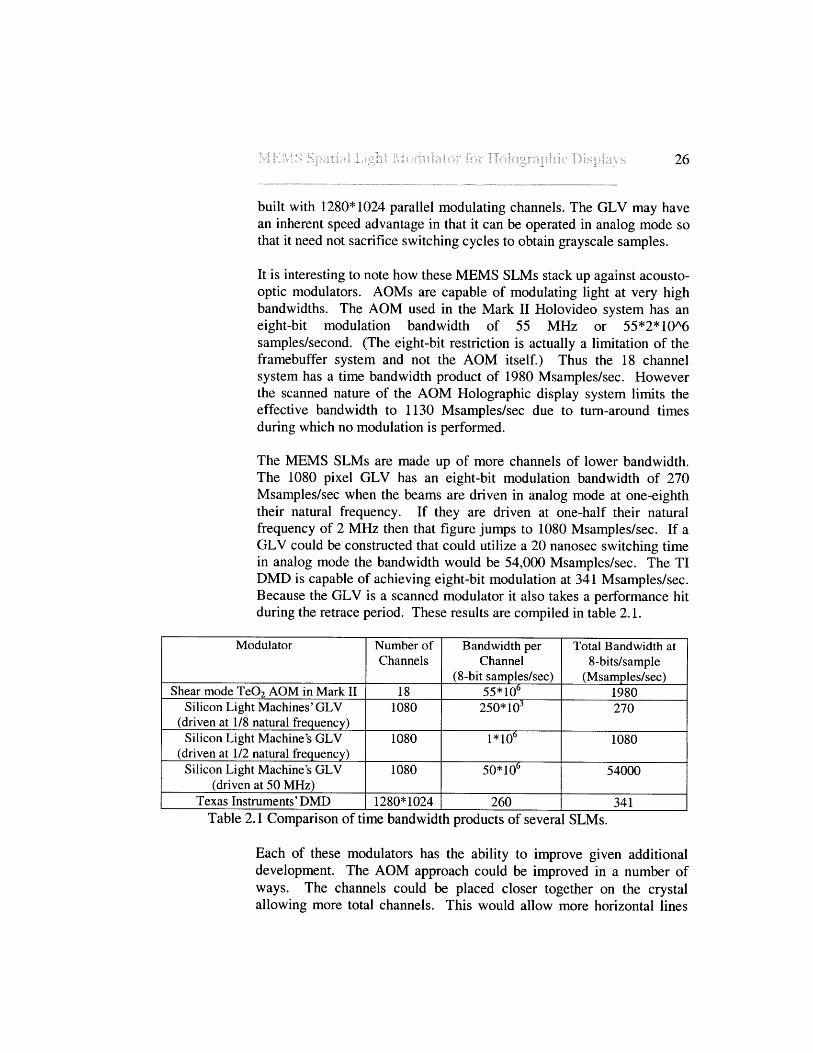
It is interesting to note how these MEMS SLMs stack up against acousto-optic modulators. AOMs are capable of modulating light at very highbandwidths. The AOM used in the Mark II Holovideo system has aneight-bit modulation bandwidth of 55 MHz or 55*2*10A6samples/second. (The eight-bit restriction is actually a limitation of theframebuffer system and not the AOM itself.) Thus the 18 channelsystem has a time bandwidth product of 1980 Msamples/sec. Howeverthe scanned nature of the AOM Holographic display system limits theeffective bandwidth to 1130 Msamples/sec due to turn-around timesduring which no modulation is performed.
The MEMS SLMs are made up of more channels of lower bandwidth.The 1080 pixel GLV has an eight-bit modulation bandwidth of 270Msamples/sec when the beams are driven in analog mode at one-eighththeir natural frequency. If they are driven at one-half their naturalfrequency of 2 MHz then that figure jumps to 1080 Msamples/sec. If aGLV could be constructed that could utilize a 20 nanosec switching timein analog mode the bandwidth would be 54,000 Msamples/sec. The TIDMD is capable of achieving eight-bit modulation at 341 Msamples/sec.Because the GLV is a scanned modulator it also takes a performance hitduring the retrace period. These results are compiled in table 2.1.
Modulator Number of Bandwidth per Total Bandwidth atChannels Channel 8-bits/sample
(8-bit samples/sec) (Msamples/sec)Shear mode TeO 2 AOM in Mark II 18 55*106 1980
Silicon Light Machines'GLV 1080 250* 103 270(driven at 1/8 natural frequency)
Silicon Light Machine's GLV 1080 1*106 1080(driven at 1/2 natural frequency)
_______W_
Silicon Light Machine's GLV 1080 50*106 54000(driven at 50 MHz)
Texas Instruments'DMD 1280*1024 260 341Table 2.1 Comparison of time bandwidth products of several SLMs.
Each of these modulators has the ability to improve given additionaldevelopment. The AOM approach could be improved in a number ofways. The channels could be placed closer together on the crystalallowing more total channels. This would allow more horizontal lines
and also give room to trade-off scan time to get longer lines. However,this approach would require the horizontal scan mirrors to sweep througha larger angle unless a longer focal length lens is used after the AOM.This angle is already constrained by the diameter of the output lens andthe abilities of the scanning galvonometers. This approach would workif a stronger output lens could be used and faster scanners found. Higherbandwidth acousto-optic materials are also available if an appropriatebalance of system components can be managed.
2.3 Feasibility of Holographic Displays based on theseMEMS-SLMsIn the previous section the MEMS SLMs have been compared to theTeO 2 AOM used in the Holovideo system without considering whetherthey are suitable for use in a practical holographic display. Given thenature of the DMD pixels it may be difficult to build a truly holographicdisplay based on that device. Even if the pixels could be made to diffractlight in a useful manner, they would need to be demagnified significantlyto provide a sufficient viewing angle.
The GLV is not much more suitable for driving a holographic displaythan the DMD. It does, however, have higher spatial frequencies andtime bandwidth products. But this is of limited use without individuallycontrollable beams.
The Polychromator was conspicuously dropped from the discussion oftemporal bandwidth because no figures relating to switching speed couldbe found. Also, because of pin-out issues only 128 of the 1024 totalbeams can be individually controlled. Thus between the unknowntemporal bandwidth, limited individual control, and limited spatialbandwidth the Polychromator appears to be an unlikely candidate forholographic displays also.
A MEMS SLM that combines the spatial resolution and switching speedof the GLV and the addressability of the Polychromator could be apotential contender in the quest to build the next generation ofholographic display. The next chapter describes a prototype holographicdisplay designed to use just such a device. In chapter 5 improvements onextending the MEMS-based holographic display to a larger scale areproposed.

28

3. System Design
The design of the MEMS diffractive spatial light modulator began in aMedia Arts and Sciences MEMS project class co-taught by ProfessorsScott Manalis and Marty Schmidt. The intent of the class was tointroduce the members to MEMS design and fabrication by creating aMEMS-based holographic display. The display would consist of aMEMS spatial light modulator, a MEMS array of scanning mirrors,imaging optics, and drive electronics. The project team was looselyassigned as follows: James White and Guy Rasmuth took primaryresponsibility for the MEMS scanning mirror array, Matt Reynoldsdesigned the drive electronics, Yael Maguire, Diana Young, and ElroyPearson took care of the MEMS SLM, and Elroy Pearson designed theoptical layout.
The design process began with a system level design. It was decided thatthe system would follow the basic optical principles used in the MITMark I Holographic Video system with a few exceptions. The lightmodulator would be constructed following the plans of the Grating LightModulator built by Solgaard, Sandejas, and Bloom6 . Previously an AOMhad been used as the SLM. The spinning polygonal mirror would bereplaced by an array of scanning mirrors as was done in the Mark IIdisplay. These scanning mirrors would also be MEMS devices. Customelectronics would be built to drive the SLM, the mirror array, and avertical scanning mirror.
3.1 SLM Design
3.1.1 SLM Mechanical and Electrical DesignThe capabilities of the SLM and scanning mirror array determined manyof the properties of the optical subsystem and the drive electronics andvice versa. In the Solgaard paper that we followed, several sizes ofbeam arrays were constructed. We decided to make the beam width justslightly larger than the feature size allowed by the lithography equipmentavailable in the Microsystems Technology Lab (MTL) at MIT. Sincethe achievable feature size was estimated to be around one micron wedecided to make the beams 1.5 microns wide. The length of the beamswas chosen to be 100 microns long. Solgaard measured the naturalfrequency of beams of this size to be 1.5 MHz. Because tension is the

major restoring force in the beams, they can be approximately modeledas vibrating strings. Thus the resonant frequency can be found from
F 2L 3.1
where L is the length of the beam, ao is the tensile stress, and p is thedensity. According to Kovacs" low-stress nitride has a density of 2.9 to3.1 g/cm3 and a stress of 1000 MPa. He notes, however, that low-stressnitride can have stresses approximately equal to 0 Pa. Commercial thinfilm deposition services list nitride stresses between 110 and 160 MPa.A quick calculation with 1000 Mpa stress shows a resonant frequency of2.9 MHz. A stress of 100 MPa would yield a resonant frequency of .928MHz. One lesson here is that processes can vary widely and numericalanalysis of a MEMS part is only valid if the figures used have been wellcharacterized. A value in a table in a book cannot blindly be used to giveaccurate predictions of performance unless the process available to theuser has well known results. However, numerical analysis can help oneunderstand generally the effects of a process change on the finishedproduct even when specific data are not yet available. So a prudentMEMS builder will not assume a process will work until experience hasshown her it will.
Unfortunately for the design of the MEMS SLM we had to make the bestguess we could on several material values. Because we didn't have soliddata on the stress level of nitride available through the MTL, we had topick a value and hope that we could adjust the processing or drivevoltage parameters until we achieved the desired results. The beamsneeded to be deflected at least wavelength of light (158 nm for 633 nmlight). The thickness of the beams was set at 158 nm to follow theSolgaard design. Next the initial gap distance g, between the beam andbottom electrode had to be set. Here we varied from the Solgaard designso that the beams could travel the full 158 nm without experiencing"pull-in". Pull-in is a state in which the electro-mechanical forcesbecome unstable and the structure spontaneously collapses to the bottomof the substrate without increased voltage. The regions of travel can beseen in figure 3.1. According to Senturia 2 the pull-in distance for abeam that is approximately one-half as thick as the gap g0 is one-third g.For a beam that is thinner the stable travel distance increases slightlybecause of "strain-stiffening". This is because as the beam bends the
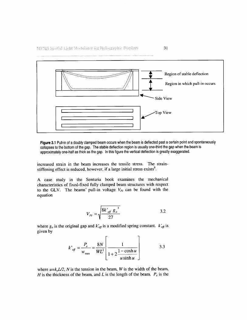
Figure 3.1 Pull-in of a doubly clamped beam occurs when the beam is deflected past a certain point and spontaneouslycollapses to the bottom of the gap. The stable deflection region is usually one-third the gap when the beam isapproximately one-half as thick as the gap. In this figure the vertical deflection is greatly exaggerated.
increased strain in the beam increases the tensile stress. The strain-stiffening effect is reduced, however, if a large initial stress exists8 .
A case study in the Senturia book examines the mechanicalcharacteristics of fixed-fixed fully clamped beam structures with respectto the GLV. The beams' pull-in voltage Vpe can be found with theequation
V = 8 k',f go 3.2P 27
where g is the original gap and k'eg is a modified spring constant. k' isgiven by
Pe 8N 1 1k'ff = -=-c3.3
e mwx WL 2 1+21 coshuusinhu
where u=kU2, N is the tension in the beam, W is the width of the beam,H is the thickness of the beam, and L is the length of the beam. Pe is the
- ::::....::::.--.7... Region of stable deflection
Region in which pull-in occurs
Side View

effective pressure on the beam and w,mo is the deflection of the beam atthe point of greatest travel - the center. The previous variables are foundthrough the following equations
N =o-WH 3.4
eV 2P = v2 3.5
e2(go - W.)2
qL L 2 cosh(k0LI2)-' 3.6"""x4N 2 ko sinh(ko L / 2)
k 12N 37k = 3.EWH3
where E is the Young's modulus, and V is the voltage between the beamand the electrode that forms the bottom of the gap. q is the distributedload on the beam or force per unit length so it is just the effectivepressure P, times the beam width W. These equations use a parallel plateapproximation that can be improved somewhat using more sophisticatednon-linear numerical simulations. The pull-in voltage in particular is offby about 20%, but is close enough to give one an idea of the effects ofchanges in geometry and drive voltage on the system.
Using these equations we can see what region of operation our choices ofbeam structure and geometry places us in. Because the residual stress Uois a parameter that has to be determined empirically it is important toknow what effect it has on the final performance. Figure 3.2 shows thechange in pull-in voltage versus residual stress for a nitride beam 100microns long, 1.5 microns wide, and .15 microns thick with an initial gapg of 1 micron.

4.5 30
25-
.C7.
75 77
5-435 120-
3 0
0 0.5 1 1.5 2 0 0.5 1 1.5 2
Residual Stress (Pa) x106 Residual Stress (Pa) x10 8
Figure 3.2 These graphs show the pull-in voltage versus the residual stress in the beam. Becauseresidual stress in nitride can vary greatly the left figure shows the pull-in voltage for stresses between 0and 2 MPa and the right figure shows the pull-in voltage for stresses between 1 and 200 MPa.
From these simulations it is apparent that the range of pull-in voltages forlow-stress nitride beams could vary from about 3 to 29 volts. Typicalnitride stress values available commercially through mems-exchange.orgare between 110 and 160 MPa. This leads to pull-in voltages betweenabout 17 to 26 volts.
The operational voltage, or voltage required to deflect the beams 14,determines the range required of the digital-to-analog converters that willdrive the beams. It can be found by solving equations 3.5 and 3.6 for V.
8N(go -Wmax) 2Wmax
3.8
4L_ cosh(k
0L/2)-2 ko sinh(koL / 2)
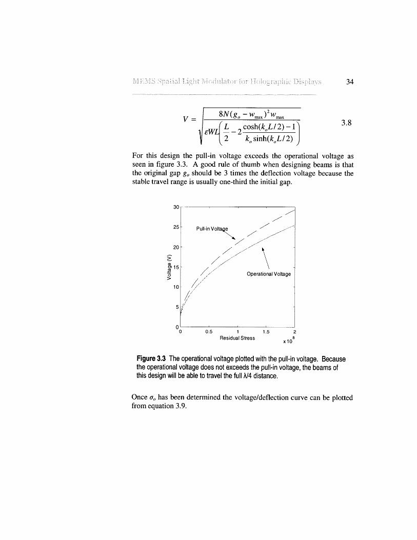
For this design the pull-in voltage exceeds the operational voltage asseen in figure 3.3. A good rule of thumb when designing beams is thatthe original gap go should be 3 times the deflection voltage because thestable travel range is usually one-third the initial gap.
0150
0.5 1Residual Stress 8
X10
Figure 3.3 The operational voltage plotted with the pull-in voltage. Becausethe operational voltage does not exceeds the pull-in voltage, the beams ofthis design will be able to travel the full A/4 distance.
Once o-, has been determined the voltage/deflection curve can be plottedfrom equation 3.9.
P ull-in Voltagta
Operational Voltage
V =

2
Z2 +gz2 __ =0 3.92 keff
The first root of 3.9 gives the deflection distance where z=w,,,x. Thevoltage/deflection curve for a beam with the dimensions as usedpreviously and residual stress of 110 MPa can be seen in figure 3.4.
x10
9.5 F
8.5 -
7.5
7
0 5 10 15Voltage (V)
Figure 3.4 The voltage/deflection curve for a beam with residualstress of 110 MPa.
3.1.2 SLM PinoutOnce the operational voltage level is determined a digital-to-analogconverter (DAC) can be chosen. The DAC must have a high enoughvoltage rating to be able to deflect the beams through the entire V/4
distance. Also important is the resolution of the DAC. To control the
Pull-in
6.
36
beams to 256 discrete levels a DAC with 8 bits of precision is required.However, more bits are likely to be required in order to make equaldeflections throughout the stable travel distance because equal voltagechanges at distances close to the full gap and the pull-in level will movethe beam unequal amounts.
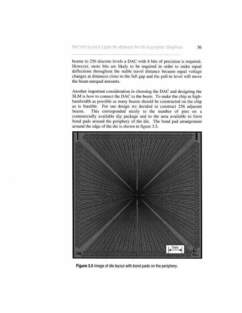
Another important consideration in choosing the DAC and designing theSLM is how to connect the DAC to the beam. To make the chip as high-bandwidth as possible as many beams should be constructed on the chipas is feasible. For our design we decided to construct 256 adjacentbeams. This corresponded nicely to the number of pins on acommercially available dip package and to the area available to formbond pads around the periphery of the die. The bond pad arrangementaround the edge of the die is shown in figure 3.5.
Figure 3.5 Image of die layout with bond pads on the periphery.

Figure 3.6 Close-up views of beam array. The left images shows the entire array of 256 beams withattached leads spreading out to the bond-out pads. The right image shows the leads connecting to theelectrodes on adjacent beams from opposite sides.
Each bond pad is connected to a metal trace that conducts electricity to asingle beam in the center of the die (figure 3.6). Traces to the electrodeson adjacent beams approach the beams from opposite side of the array.This allows a smaller tolerance for the traces during patterning. Eachbeam is 1.5 microns wide by 100 microns long with gaps 1.5 micronswide between pairs of beams. The traces are 3 microns wide with spaces3 microns wide between them.
3.1.3 SLM Microfabrication Process DesignThe physical size and composition of the beams were chosen to utilizeequipment available in the MIT Microsystems Technology Laboratory(MTL). The processing of this devices involves applying various layersof materials to a single crystal silicon wafer and then patterning thoselayers with a variety of lithography techniques and etches. The originaldesign called for nitride beams to be constructed on a silicon dioxidesacrificial layer with gold electrodes, traces, and bond pads. Due toprocessing difficulties this was changed to a process with nitride beamson a polysilicon sacrificial layer with gold electrodes, traces, and bondpads. The reasons for the switch are explained in chapter 4. This chapterdiscusses only the polysilicon process.
The process starts with growing 100 nm of oxide on an n-type siliconwafer that is 500 microns thick. Then a layer of polysilicon is deposited

via low-pressure chemical vapor deposition (LPCVD) to a thickness ofone micron. A 158 nm thick layer of low-stress silicon nitride is thendeposited on top of the polysilicon. A cross-sectional view of theselayers is shown in figure 3.7. All of the materials are also deposited tosome degree on the backside of the wafer though they are not shown
NitridePolysiliconOxideSilicon
Figure 3.7 Growth of 100 nm oxide layer anddeposition of 1 micron polysilicon layer and 158nm nitride layer.
here.To prepare the wafer for the first mask layer the nitride, polysilicon, andoxide layer are etched from the backside. Thus nothing need touch thefrontside of the wafer after it has been patterned.
The first mask layer patterns trenches the length and width of the beamsin the center of the die. To prepare the wafer for the etch it is coated inphotoresist. Photoresist is a light sensitive material that can be patternedwith light and then chemically developed such that the patterned areaswash away. Positive photoresist washes away in the places that havebeen exposed to light. Negative, or image-reversal, photoresist washesaway in the places that haven't been exposed to light. The remainingmaterial is then baked to form a hardened mask. This mask is resistant tomany chemicals, so places that are covered in resist are protected fromthe etchant while areas without resist are etched. This process usespositive photoresist.
Photoresist is deposited in liquid form onto a spinning wafer. Thisspreads the resist into a thin, uniform layer on the wafer. The wafer isthen baked to pre-harden the resist before exposure. The wafer is thenexposed to light that has been spatially modulated in the proper pattern.After exposure the wafer is developed and then post-baked to harden theresist mask. The post-baked photoresist pattern from the first mask layeris shown in figure 3.8.

Figure 3.8 Wafer after photoresist exposure to first mask layer and development.
After the resist is developed and hard-baked the nitride and polysiliconlayers are etched in a plasma etcher. The plasma etcher uses etchantchemicals under vacuum in a high powered RF field to etch verticallyoriented sidewalls. This is known as anisotropic etching because itfavors removing material in one direction over another. Isotropic etchingremoves material in all directions at the same rate and thus makes dish-shaped etches rather than box shaped etches. The etched wafer in figure3.9 shows the results of the anisotropic nitride and polysilicon etches.After the trenches are etched in the nitride and polysilicon layers, thefirst laver of Dhotoresist is removed. Then a second laver of Dhotoresist
Figure 3.9 Wafer after anisotropic nitride and polysilicon etches in plasma etcher.

is applied and pre-baked. Into this layer of photoresist is exposed thesecond mask layer. This is the layer that defines the beam electrodes,leads, and bond pads. This layer is known as a "lift-off metal layer". Thephotoresist is patterned to stay where the gold is to be removed. Thengold is evaporated onto the photoresist and exposed areas of the wafer.The wafer is then soaked in an acetone bath to dissolve the photoresistand lift off any metal that was deposited on the resist. Figure 3.10 showsthe photoresist pattern on the beams. Figure 3.11 shows the metaldeposition and then liftoff steps. Before the 50 nm gold layer isdeposited a 10 nm layer of Titanium is put down. This helps the goldadhere to the underlying nitride.
.. __---__...-------------- - - -
' I.
Figure 3.10 Wafer after lift-off photoresist has been developed, but before deposition of the metal layer.
NitridePolysiliconOxideSilicon
I

- - - - - - - - - - - ---
- - -
10 X
------------.. --- - -
Figure 3.10 The top image shows the wafer after metallization. The bottom picture shows the waferafter the wafer has been put in acetone, the photoresist dissolved, and the metal patterned by lift-off.
L -- J.Gold/TitaniumNitridePolysiliconOxideSilicon
Gold/TitaniumNitridePolysiliconOxideSilicon
L . ... _I
3 'J I A z -'. E .1 .1 A l

K
There are a couple of key assumptions in this liftoff process. The first isthat the profile of the liftoff photoresist will be steep enough to makesure that the gold on top of the photoresist is not connected to the gold onthe wafer. The second assumption is related. It is that sidewalls of thenitride-polysilicon trenches are straight enough that the gold on the topof the beams does not connect to the gold on the bottom of the trenches.The next chapter will discuss the impact of these design decisions.
The next fabrication step is to thicken up the bond pads. The traces areconnected by gold wire bonding to the chip package. For the wirebonder to work a thicker layer of gold is required on the bond pads. A200 to 300 nm thick layer of gold is needed to promote good adhesion bythe gold connection wires. This thicker layer of gold is applied in asecond liftoff process. In this process the only holes patterned into thephotoresist are holes above the bond pads. Then a thick layer of gold isdeposited and removed in an acetone bath as before (figure 3.11).
Figure 3.11 The 100 micron wide bond pads at the edges of the die are thickened up with a secondlayer of gold to help the gold wires to adhere to the pads better during wirebonding.
Once the second liftoff is completed successfully the beams can bereleased. The beams are released in a dry Xenon Difluoride (XeF 2) etch.
2nd layer of gold gold-titanium layer

NI I 4
The XeF2 etches the polysilicon sacrificial layer from under the nitridebeams (figure 3.12).
Figure 3.12 The nitride beams are undercut by etching the sacrificial polysilicon layer with a Xenon Difluoride etch.
After the beams have been released, the wafer can be sawed intoindividual dies. The dies are then mounted into chip packages and wirebonded to the electrical connections. At that point the MEMS SLM isready to be integrated into the full holographic display.
3.1.3 SLM Optical AnalysisThe MEMS SLM modulates light through diffraction as does the SiliconLight Machines' GLV. However, a more complex model of thediffraction is needed for analysis of the optical characteristics of thisMEMS SLM because every beam is individually controllable. Also
I - ------ -- -- -- --

Thickness2 pm0.667 pm
2 pm.25 pm2 pm
2 pm0.5 pm
Phase Delay
2niz/A
x
Figure 3.13 The MEMS diffractive SLM can be modeled as a phase grating.The local phase delay introduced by a deflected beam is equal to 4*T*wm/A.
hologram computation for the completed display will be based on thediffraction model used for analysis.
The MEMS SLM is essentially a one-dimensional dynamic surface reliefgrating. When the beams are all in the same plane light reflects off thefront of the beams as it would off a mirror (except for the extraneousdiffraction added by the spaces between the beams). When two adjacentbeams are at different heights, the light bouncing off the lower beam isdelayed in phase by
2ff#=- 2wmax 3.10
A
where 2 is the wavelength of light. The resulting grating pattern can bemodeled as a transmission phase grating (figure 3.13). A basic square-wave phase grating works by retarding light wavefronts as a function ofposition 13. Because a phase grating absorbs no light the diffractedefficiency can reach 100 percent when all of the diffracted orders arecollected. Up to 40.5 percent of the light can be contained in each of thefirst orders. The diffraction efficiency DE of the orders m can becalculated as

DEm = cos 2 Ag
DEm±i = c sin A#j
DEm even =0
DEm DEm
3.11
3.12
3.13
3.14
where A P is the phase delay. Of course these equations are for squarewaves only so a more complete model would take into account themovable beams and the immovable dead-space in between. Far-fielddiffraction effects can be determined by treating each beam or space as aone-dimensional aperture of width W with a constant phase across itswidth and then summing the contribution from all of the apertures in thefar-field. The light amplitude A(x) from each aperture leaves the SLMplane as a square wave or rect funtion (figure 3.14). In the far-field thelight amplitude from position x is distributed as a sinc function or Fouriertransform of the rect funtion due to diffraction and interference effects.This far-field amplitude at x' which originated from position x in theSLM plane is denoted A '(x-x'). This distribution is given by
A'(x -> x') = A(x)W sinc 3.15
where the angle between x and x' is 0 which is equal to atan((x'-x)/(z+2wa)). The phase of the light is given by equation 3.16.
x x'
z z
A(x) z
2wmT ....
SLM Plane Far-field plane
Figure 3.15 Light propagates from the SLM plane on the left to the far-fieldplane on the right.
-Fm4- W
A
Propagation of lightthrough an aperture
A(x)
Ao
xAmplitude at aperture
A'(0)
AIWFar field amplitude
Figure 3.14 The farfield intensitydistribution emanatingfrom a rectangularaperature is a sincfunction.
F27T(z+2wmna)1F'(x -> x') = jsin[ + cos(O)J 3.161 A cos(6)
The complex amplitude contribution E'(x--+x' from the aperture atposition x in the SLM plane to the position x' in the far-field is acombination of equations 3.15 and 3.16.
E'(x -> x') = A'(x -> x')+cF'(x -+ x') 3.17
The total amplitude E' otaI(x') at the point x' is found by sunning thecontributions E'(x--+x) from every point in the SLM plane x.
X /2
E'total (x') = 1 E'(x -> x') 3.18x=-X /2
This summation would then be convolved with the lower frequency sincfunction that results from the combined aperture of the entire beam array.
3.2 Optical Architecture DesignThe purpose of the optical architecture is to form the light modulated bythe SLM into a three-dimensional holographic image. The hologram iscreated by increasing the effective aperture of the SLM by tiling itsimage in the output plane of the display. This is accomplished in muchthe same way as the MIT Mark II holographic display. A verticalscanning mirror scans the image vertically and a bank of horizontalmirrors scan the image horizontally. Lenses demagnify the image tocreate a sufficient viewing angle. The optical layout is shown in figure3.15.
Most of the lens requirements can be reduced to geometric relationships.The laser illuminates the SLM at normal incidence. The highest anglethat the SLM can diffract light is found from the grating equation,
ft=sin6. The highest frequency that this grating SLM can synthesize isone half the spatial frequency of beams or 166 lines per millimeter. Thisleads to the first order being diffracted at 6 degrees. By placing the SLMat the focal length of a lens LI the light will be nearly collimated withthe spatial frequency transformed to a spatial offset along the horizontalaxis. The focal length of LI dictates the minimum width of the verticalscanning mirror and the minimum combined width of the horizontal

'ZU 1 ' ,
Figure 3.15 The optical layout of the MEMS Holographic Display.
scanning mirrors. Because the width of the scanning mirrors was set to 2cm a lens of focal length 18.85 cm is needed.
Figure 3.16 The width di is set by the focallargest diffraction angle 0, of the SLM.
length of lens Li and the
The total size of the array of scanning mirrors is 2 cm wide by 3cm tall.They are designed to scan 5 mechanical degrees so they deflect 10optical degrees (figure 3.17). The final imaging lens needs to have an

02 = 10 degrees
f =o= 5degrees
Figure 3.17 The optical angle 82 is twice the mechanicalangle of the horizontal scanning mirrors.
aperture wide enough to capture all of the light deflected by the mirrors(figure 3.18).
The vertical optical system scans the image line through a cylindricallens L2 which focuses the line at the center of the horizontal scanningarray. The unfolded vertical system in figure 3.19 shows that the lightleaving the horizontal scanning area will be collimated parallel to theoptical axis. The height of the image is controlled by the scan angle ofthe vertical scanning mirror.
f
horizontal scanningmirror array .. ........................ 4
Vertical diffuserimaging lens L3
Figure 3.18 Top view of the last half of the holographic display optical layout. The horizontal scanningmirror array is placed at the focal length of lens L3 which images the SLM at the vertical diffusing plane.

4- 2f2 -- 4- 2f2 -- 10
SLM Vertical hoiotlzL2 hori .zontalLi Scanning scanning array L3 vertical
Mirror diffuser
Figure 3.19 Side view of unfolded vertical optical system.
3.3 SummaryA complete holographic display was designed in the MEMS projectclass. Designs were submitted for the drive electronics, horizontalscanning mirror array, the optical architecture, and the MEMS SLM.Much progress was made in developing the fabrication techniquesrequired to build the MEMS devices.

50

4. Processing
4.1 Process Overview
4.1.1 Chapter ContentsChapter 4 discusses the practical considerations of process developmentfor the MEMS SLM. Both the oxide sacrificial layer process and thepolysilicon sacrificial layer process are presented side-by-side. Thisallows a concise comparison of characteristics of the processes. Duringthe development of this process most of the steps were performedrepeatedly until they became well characterized. However, thepolysilicon process' gold electrode application step still remains to becharacterized. Most of this chapter describes how to perform processsteps that are proven to work. At the end of the chapter the focus shiftsto suggestions on perfecting the remaining steps.
The majority of the steps carried out in this chapter are performed inclass 100 or class 10 clean rooms. The class number of the clean roomspecifies how many one micron particles per cubic foot of air are present.Clean conditions reduce the number of imperfections in the process bykeeping dust particles off the wafers. A dust particle can wreak havocwith a microfabrication project because it can interfere with properimage patterning and etching.
Chapter 4 is divided into six sections. These sections cover thin filmgrowth and deposition, photolithography, plasma etching, metal liftoff,release etching, and packaging.
4.2 Thin Film Application
4.2.1 Thermal Oxide GrowthThe first step in both the oxide sacrificial layer process and polysiliconsacrificial layer process, hereinafter referred to as the oxide process andthe poly process respectively, is to grow a layer of thermal oxide. Theoxide process calls for a micron thick layer of silicon dioxide to act asthe sacrificial layer. The poly process requires only 100 nm of silicondioxide for an etch stop for the polysilicon layer.

Thermal oxide is grown in a thermal oxidation furnace. To prevent tubecontamination the wafers are first cleaned using an RCA clean14 toremove any organics, native oxide, and ionic or heavy metalcontaminants. The RCA clean was first developed by RCA Laboratoriesin the 1970's and has now become an industry standard 5 . The RCAclean has three major steps. The organics are removed with a 5:1:1H20:H20 2:NH40H solution. Then the native oxide is remove in a diluted50:1 H20:HF etch. Finally ionic and heavy metal atomic contaminantsare removed using a solution of 6:1:1 H20:H20 2:HCL. When the wafersare properly cleaned they can be placed in the oxidation furnace.
The oxidation furnace envelops the wafers in a high temperatureatmosphere of oxygen. The reaction model is
Si(s) + 0 2(g) -> SiO2(s) 4.1
A layer of oxide quickly grows at the silicon air interface. A thin layerof oxide will even grow in room temperature conditions. After the initialthin layer is grown, however, the oxide layer can only grow whenoxygen or silicon atoms pass through the existing oxide layer. Thetemperature is increased to promote diffusion. Oxygen diffuses muchfaster than silicon so the oxide grows at the oxide silicon interface.
Once the oxide layer is grown, its thickness is measured with anellipsometer. It is important to remember that oxide also grows on thebackside of the wafer because this layer must be removed before thesubstrate can be electrically connected to ground.
4.2.2 Polysilicon DepositionAfter the oxide is grown the poly process calls for a one micron layer ofpolysilicon to be deposited. Polysilicon is silicon composed of manysmall crystals rather one large crystal. The polysilicon is deposited in alow pressure chemical vapor deposition (LPCVD) furnace. The furnaceis pumped down to around 150 mTorr after being flushed with nitrogenand the temperature is raised to around 580 degrees C. The overallreaction is
SiH4(g) -+ Si(s) + H2(g) 4.2
Deposited polysilicon is not as smooth as single crystal silicon.Subsequently any layers deposited on top of it will also be rough. Theroughness is readily seen in the scanning electron micrographs in figure

MM S a Lia M a r a D
4.1, but can even be detected under an optical microscope. Futureprocesses should include a polish after the polysilicon deposition tosmooth out the surface so that the beams will be flat reflectors.
Figure 4.1 The left image is a scanning electron micrograph of the undercut beams in the oxideprocess without gold electrodes. The right image shows the beams in the poly process with goldelectrodes and traces deposited. Note that the surface of the nitride beams is much smoother forthe oxide process than for the poly process.
4.2.3 Nitride DepositionThe beam structural material is silicon nitride. 158 nm of low-stresssilicon nitride is deposited in both processes. Nitride applicationhappens in an LPCVD furnace also. Some possible nitride reactions 6
are
3SiH4(g) + 4NH 3(g) -+ Si 3N4(s)+ 12H 2(g) 4.3
3SiCl 2H2(g)+ 4NH 3(g) -> Si 3N4(s)+ 6HCl(g) + 6H 2(g) 4.4
Once the nitride is in place the wafers are ready for lithography andetching. The thickness of the nitride can be checked with anellipsometer. A wafer should be kept out of the oxide growth process sothat the nitride thickness can be measured as a single film thickness. Themore thin film layers that are present in a film stack the more difficult itis to get an accurate reading of film thickness with an ellipsometer.

Figure 4.2 If notfocused and exposedproperly the beamsbecome too narrow.The beams aresupposed to be as wideas the gaps.
54
4.3 Lithography
4.3.1 PhotoresistBefore the wafers can be etched a layer of photoresist must be patternedon the wafers to define the etch features. To improve adhesion of thephotoresist to the wafers, they are first baked in a hexamethyldisilazane(HMDS) environment . HMDS is meant to promote adhesion to oxides,but experience has shown that it helps photoresist stick better to nitridealso. If the backside of the wafer is being etched and the resist is requiredonly to protect the frontside of the wafer, the HMDS step may beomitted. After HMDS application the coater deposits liquid photoresistonto a wafer while it is spinning. This spreads the resist to a thickness ofabout one micron. After the resist is spun onto the wafer it is baked for aminute at 115 *C to preharden it. That is the final step before exposure.
4.3.2 StepperThe stepper exposes the image of a mask into the photoresist coated on awafer. Masks for the stepper are 10 cm square pieces of fused silica withchrome plated on one side. Chrome is selectively ablated with an e-beam to create the desired pattern. The stepper actually demagnifies themask image to 1 cm square. This small image covers only a portion ofthe wafer so the stepper tiles the image across the wafer repeating it in atwo-dimensional, 8x8 array.
When fabricating features about the same size as the resolution limit ofthe stepper (-1 Im), the focus and exposure time of the tool must becarefully calibrated. A test wafer receives an array of images withvarying exposure times and focus levels. After development the die withthe clearest pattern dictates the proper exposure time and focus. Becausethe lens produces a slightly curved image surface on the wafer, the edgesof the dies tend to have a different focus than the center of the image.Thus the best die on the test wafer should be chosen by looking at thecritical features on the die. During development of the MEMS SLMprocess, choosing the exposure time and focus by looking at features onthe periphery caused the beams in the center of the die to be out of focusand too narrow as shown in figure 4.2. After being exposed, thephotoresist is developed and then postbaked. The postbake step furtherhardens the photoresist so that it becomes a durable etch mask.

4.4 Plasma Etching
4.4.1 Nitride EtchThe layers on the wafer get etched in the opposite order than they were
applied. The first etch steps are performed in a plasma etcher. Theplasma etcher breaks down gases into chemically active componentswith a high power RF plasma. For this process CF4 enters the chamberto etch trenches in the nitride at 350 watts. If the right balance ofchemistry and RF power is used, nearly vertical sidewalls can be etched.The speed of the etch can be characterized by measuring the nitridethickness on the ellipsometer before and after the etch.
4.4.2 Oxide EtchIn the oxide process a chemistry of CF4 and CHF3 etches the sacrificialoxide at 350 watts.
4.4.3 Polysilicon EtchAchieving straight sidewalls with a polysilicon etch is challenging. Anetch using HBr and Cl2 at 300 watts seemed to attack the photoresist andetch the nitride such that it produced slanted sidewalls. Figure 4.3 showsthe slanted sidewalls formed by this etch. The sidewalls shown in theright figure were produced by etching first with HBr and Cl2 at 300 wattsand then with just HBr at 100 watts. Using only HBr for the entire etchshould create much more vertical sidewalls.
The sidewalls of the sacrificial layer must be perfectly vertical or evenslightly undercut for the metal deposition. If the walls are slanted at allthen the metal will cover them and connect the bottoms of the trenches tothe tops of the beams. This will prevent the beams from being freedwhen the final release etch is performed. Even perfectly verticalsidewalls may not prevent gold from covering the sidewalls.

Figure 4.3 A plasma etch with HBr and C12 of the polysilicon layer on the left. The etch also attacksthe photoresist and the nitride which creates slanted sidewalls. The etch on the right used C12 onlyduring the first part of the etch, but completed using just HBr.
4.5 Metal Liftoff
4.5.1 KOH Etch of PolysiliconTo prevent the sidewalls from getting covered in gold, the polysiliconmust be isotropically etched to slightly undercut the beams. The etchshould be timed precisely so that it will not entirely undercut the beamsand release them. If they were released early the beams would probablybecome stuck to the bottom of the trench due to stiction duringsubsequent wet processing. Figure 4.4 shows the results of slanted andvertical sidewalls in the left picture and the desired results of a slightundercut in the right image.
Figure 4.4 The beams in the SEM image on the left have gold on the sidewalls even though they arenearly vertical. Also the gold seems to bridge across the trench in the trench second from the left. Inthe right image the gold shouldn't cover the sidewalls if they slightly undercut the beams.
The KOH etch needs to be properly characterized before it can be usedwith confidence in this process. After the KOH etch and before thelithography for the metal liftoff the wafers must go through an extensivecleaning process. Three separate "piranha etches" clean the wafers sothat they can be placed back into the photolithography equipment. Apiranha etch is the first step of the RCA clean except with a 7:3 mixtureof sulfuric acid to hydrogen peroxide.
4.5.2 Stepper Lithography for LiftoffThe lithography for metal liftoff is the same as for etching except that thepost-bake is omitted from the liftoff procedure. Hard baking photoresistcan cause it to reflow slightly, which rounds the photoresist features. Bynot post-baking the photoresist it keeps sharp features and dissolves moreeasily in acetone later. For thicker metal layers, image reversalphotoresist may give better liftoff results. Image reversal liftoff washesaway in areas not exposed to light.
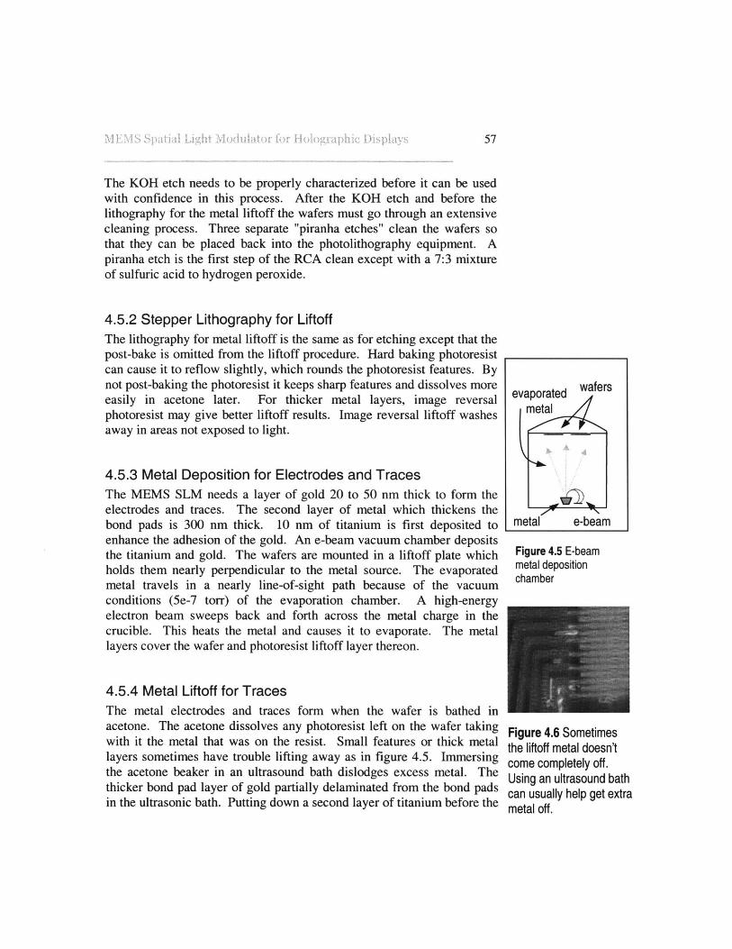
4.5.3 Metal Deposition for Electrodes and TracesThe MEMS SLM needs a layer of gold 20 to 50 nm thick to form theelectrodes and traces. The second layer of metal which thickens thebond pads is 300 nm thick. 10 nm of titanium is first deposited toenhance the adhesion of the gold. An e-beam vacuum chamber depositsthe titanium and gold. The wafers are mounted in a liftoff plate whichholds them nearly perpendicular to the metal source. The evaporatedmetal travels in a nearly line-of-sight path because of the vacuumconditions (5e-7 torr) of the evaporation chamber. A high-energyelectron beam sweeps back and forth across the metal charge in thecrucible. This heats the metal and causes it to evaporate. The metallayers cover the wafer and photoresist liftoff layer thereon.
4.5.4 Metal Liftoff for TracesThe metal electrodes and traces form when the wafer is bathed inacetone. The acetone dissolves any photoresist left on the wafer takingwith it the metal that was on the resist. Small features or thick metallayers sometimes have trouble lifting away as in figure 4.5. Immersingthe acetone beaker in an ultrasound bath dislodges excess metal. Thethicker bond pad layer of gold partially delaminated from the bond padsin the ultrasonic bath. Putting down a second layer of titanium before the
Figure 4.5 E-beammetal depositionchamber
Figure 4.6 Sometimesthe liftoff metal doesn'tcome completely off.Using an ultrasound bathcan usually help get extrametal off.

second layer of gold may help the gold stick better. After the metal haslifted off, the wafer is rinsed in DI water and dried from the center outwith compressed nitrogen. For difficult liftoff patterning it was foundthat applying an adhesive tape (in this case Scotch Tapem) and peeling itoff removed the liftoff metal very well. Perhaps a clean roomcompatible version of this liftoff could be developed.
4.6 Release Etch
4.6.1 Release EtchDifficulties in the release etch motivated switching from the oxideprocess to the poly process. The original process called for the oxidesacrificial layer to be isotropically etched in HF acid to release thebeams. Two complications arose. Because HF attacks titanium the goldelectrodes and traces quickly delaminated from the die. Also the surfacetension from the wet etch pulled the beams down to the substrate causingthem to stick and not release. Releasing the beams in HF vapor was alsotried but again the metal surface was attacked quickly leaving the surfacemottled.
The polysilicon process utilizes a release etch that is becoming morefamiliar in MEMS - a xenon difluoride dry release. For this etch a waferis placed in a chamber filled with XeF2 gas which etches the polysiliconisotropically. This etch worked well to release the nitride beams thatweren't coated in gold. As stated above the gold covering the sidewallsof the coated beams prevents them from moving. Figuring out a way toprevent gold from sticking to the sidewalls of the trenches will be key togetting this process to work.
4.7 Packaging
4.7.1 PackagingAfter the dies are successfully patterned and released they must bepackaged. The first step of packaging is die sawing the wafer intoindividual dies. This mask set produces an eight-by-eight array of dieson each wafer. Three dies in each corner of the array are clipped by theedges of the wafer. Thus each wafer can potentially produce 52functional MEMS SLMs. After the die saw cuts up the wafer each die isplaced in a 256 pin package. Each bond pad is then individually gold

59
wire bonded to a pin. Electrical contact with the bottom electrode ismade through the back of the wafer. The back of the wafer is set at zerovolts.
4.7 ConclusionEach step in the oxide process and the poly process are crucial tocreating a working device. Many steps were well characterized in boththe oxide process and the poly process. The lithography, liftoff, andrelease steps of the poly process were worked out well. The sidewalletching of the polysilicon is a major issue that has not been properlyresolved, but suggestions for working out solutions to this problem havebeen presented.

60

5. Conclusions and Suggestions for FutureWork
5.1 Review
5.1.1 Thesis ReviewIn the pursuit of truly convincing visual communications, many solutionshave been imagined. A few have enjoyed relative success, but far morehave fallen short of their intended goals. This thesis has reviewed thetechnology of a few holographic displays. A variation on the Scophony-style holographic display has been presented. The capabilities of severalspatial light modulators were compared. A MEMS diffractive gratingwas built in conjunction with this work, however, more fabricationchallenges remain before we may arrive at a useable solution. Theprocess techniques have been presented to encourage completion of thedevice.
5.2 Suggestions for Future WorkFollowing is a suggestion for a scalable MEMS SLM based holographicdisplay. If an SLM can be built on the same substrate as multiplexingcircuitry, then the SLMs could be tiled very closely together to form avery long one-dimensional array of diffracting beams. If a sufficientlylong line can be tiled together then horizontal scanners would no longerbe required to build MEMS-based holographic display. A single longvertical scanning mirror could scan the entire line. By coupling thissetup with a concave mirror to refocus the image, a complete display canbe made. The suggestions for implementing this display fall under foursections: SLM fabrication, electronics configuration, and optical systemdesign.
5.2.1 SLM FabricationOne shortcoming of the SLM presented in this thesis is that only a smalllength in the center of the beams is effectively available to diffract light.This happens because the beams curve when they are bent so that thephase delay away from the center of the beams is less than that in thecenter where the deflection is greatest. This means that input light mustbe focused down to a very small line centered on the middle of the

Column To Beam
Row-
Transistor
Capacitor
Figure 5.1 Circuitryrequired to drive onebeam.
beams. Longer flat beams like those used in the Polychromator wouldallow the focus of the line to be relaxed. However, the added complexityof the Polychromator process is not attractive. Here I present apotentially simple fabrication process that would create longer flat areasin the beams and could alleviate problems due to wet release etching ofthe beams and sidewall metallization. The process is summarized infigure 5.2.
A silicon wafer receives an oxide layer and a nitride layer. A photoresistlayer defines the beams' shape. Ideally the beams would be wider thanthe gaps between them, for example 1 micron wide beams with .5 micronwide gaps. Trenches are then etched into the nitride layer using thephotoresist as an etch mask. The etch would likely be a plasma etch suchas CF4. The photoresist is then removed and a second resist layer ispatterned to expose only the middle of the beams (starting from about 10microns from the ends of the beams) to an HF etch. This etch exposesthe underlying single crystal silicon substrate. The wafer is then placedin a KOH etch to create a groove under the middle of the beams. KOHetches single crystal silicon along two directions much faster than thethird so that the etch is shaped like a trench. The remaining oxide underthe beam ends is then etched to fully release the beams. Because thedistance from the middle of the beams to the underlying substrate is morethan 28 microns the beams should remain released during subsequencewet etches. When the gold is deposited, there should be no problemswith the gold connecting the beam sidewalls to the bottom of the trench.
The actuation electrodes no longer act across the entire length of thebeams, but only towards the ends. This type of actuation is known asleveraged bending. Combined with the strain stiffening effect of the thinbeams the travel range of the beams should be increased past one-thirdthe original gap. This means that the silicon dioxide layer and hence thegap can be made thinner at the outset. These steps should fit into amodified cmos process.
Leveraged bending requires higher voltages to actuate a beam than fulllength actuation. When the voltage becomes too great the drive circuitrybecomes unreasonable to fabricate on the chip. A rough estimate of thedrive voltage can be arrived at by assuming that the contribution of theunactuated middle section of the beam doesn't contribute to setting thedrive voltage. Then if the beam length is set at the actuation electrodelength the pull-in voltage can be estimated as before. Figure 5.3 showsthe electrode length vs. pull-in voltage.

SLigh M xuator fry 63
After plasma (CF4) etch of nitride layer to form beams
After HF etch of middle of oxide sacrificial layer with resist in place
rM ~ ~ ~ Ma I B 1 -
~IIIz z~~IL ---------- ---- ---- ---- ---
After KOH etch of silicon substrate to form a 28 micron deep v-trench
680 pm-- 54.74
L ---------- ---- ---- ---- ---
After HF etch to get rid of sacrificial oxide and after aluminum deposition
Figure 5.2 -- New-MEMS-process-profil
Figure 5.2 New MEMS process profiles.

64
250
200
150
0
CL
50-
02 4 6 8 10
Actuation Electrode Length (m) x10-5
Figure 5.3 The effect of actuation electrode length on the pull-in voltage canbe seen here for a beam that is 100 microns long. The actuation electrodelength is the sum of the electrode lengths extending toward the middle of thebeam from the beam ends. For this simulation go = 500 nm, ao = 110 MPa,W= 1.5e-6, and H= .15e-6.
Because most of the space on the MEMS diffractive SLM presented inthis thesis is dedicated to the pin out of the electrode traces, the numberof beams that can be independently controlled is limited. If cmostransistors could be built in the available space instead, then the numberof beams could be increased. Because the beams are deflected by asimple voltage, the necessary drive electronics for each beam could bemade similar to those in an active matrix LCD. A transistor and acapacitor as shown in figure 5.1 should be sufficient to drive one beam.This circuit is addressable by rows and columns.
Addressing the beams by rows and columns would greatly reduce thenumber of bond pads required to control all of the beams. If N is thetotal number of beams on the chip then the number of bond pads requiredto column/row address the beams is 2*N-5 . If half of the beams areaddressed from one side of the die and half from the other then thenumber of bond pads becomes
bondpads = - 5.12

If the beams can be fabricated 1.5 microns wide with .5 micron gapsbetween them then 5000 beams would fit side to side on a 1-cm wide die.Thus 2500 transistors and capacitors would have to be addressed oneither side of the beam array. Each side would need 100 bond pads.This is 56 fewer bond pads than are needed to address the current design.However if these are to be tiled together very tightly then the limitingdimension is not the size of the bond pad but how closely traces on aprinted circuit board can be packed. A 2-cm wide die would fit 10,000beams across but only require 142 pads per side or 284 pads total. Thisleaves 140 microns for each bond pad.
The area available for control circuitry for each beam is the beam widthplus the gap width times the distance from the end of the beam to theedge of the bond pad. For a 1 cm wide die this is 2 gm * (5000 pm - (50pm + 140 pm)) = 9620 Rm 2. That equates to a square of silicon 98microns on a side in which to build a transistor, a capacitor,interconnects, and an isolation barrier between transistors. A TI DMDonly uses a square 17 microns on a side to house its drive transistors andaddress interconnects.
To equal the horizontal spatial bandwidth product of the Mark II display26 chips would need to be tiled together and then demagnified by afactor of 3.5. Figure 5.4 shows the layout of the die and how they wouldbe tiled together.
Figure 5.5 shows a possible optical setup using the tiled MEMSdiffractive SLMs and a single vertical scanning mirror. This setup wouldlikely be capable of thousands of horizontal hololines because it wouldscan vertically in a way similar to the horizontal scanning of the GLVtwo-dimensional projection display. Of course, this display would besubject to the same computational bandwidth problems of every otherholographic display that has been built.
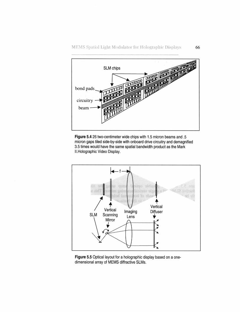
SLM chips
Figure 5.4 26 two-centimeter wide chips with 1.5 micron beams and .5micron gaps tiled side-by-side with onboard drive circuitry and demagnified3.5 times would have the same spatial bandwidth product as the MarkII.Holographic Video Display.
IVer
SLM Sca
~4f
lical Imagingnning Lens
VerticalDiffuser
Figure 5.5 Optical layout for a holographic display based on a one-dimensional array of MEMS diffractive SLMs.
bond pads.
circuitry
beam -
"Vik"A"HI 10 T" 61

5.3 Conclusions
5.3.1 ConclusionsHolographic display technology is a challenging and exciting new visualmedium. The art and science of building holographic displays willcontinue as light modulating methods are explored. A MEMS diffractiveSLM may be a significant addition to the tools that electro-holographershave to work with. As the right complement of tools becomes availablethese researchers should be able to give to the world a new means ofcommunication. When holographic displays become commonplace ourcommunications abilities will improve dramatically (and husbands stillwon't understand what their wives are telling them).
The End of a Beginning

References
1 M. L. Jepson, "Holographic Video: Design and Implementation of a DisplaySystem", Masters Thesis, MIT Media Laboratory, June 1989.
2 P. St-Hilaire, "Scalable Optical Architectures for Electronic Holography",Masters Thesis, MIT Media Laboratory, September 1994.
3 Okolicsanyi, F., Wireless Engineer, 14, 527, 1937.
4 Robinson, D. M., Proc. I.R.I, 27, 483, 1939.
5 Jeon, Hyung-Wook, A. R. L. Travis, N. Collings, T. D. Wilkinson, and Y.Frauel, "Image tiling system using optically addressed spatial light modulatorfor high-resolution and multiview 3-D display," Proc. SPIE, Vol. 3957, 2000.
6 Solgaard, 0., Sandejas, F. S. A., and Bloom, D. M., "Deformable GratingOptical Modulator," Optics Letters, vol. 17, no. 9, May 1, 1992, pp. 688 - 690.
7 Hornbeck, L. J., "Digital Light Processing: A new MEMS-based displaytechnology," Technical Digest of the EIIJ 14* Sensor Symposium, pp. 297-304.
8 Hung, E. S., Senturia, S. D., "Extending the Travel Range of Analog-TunedElectrostatic Actuators," Journal of Microelectromechanical Systems, 8, 497,1999.
9 Amm, D. T., R. W. Corrigan, "Grating Light Valve Technology: Update andNovel Applications," Society for Information Display Symposium, May 1998,Anaheim, CA.
10 Bloom, D., "The Grating Light Valve: Revolutionizing Display Technology,"Projection Displays III Symposium, SPIE Proceedings Volume 3013, San Jose,CA February 1997.
" Kovacs, Gregory T. A., "Micromachined Transducers Sourcebook",McGraw-Hill, 1998.
12 Senturia, Stephen D., "Microsystem Design", Kluwer Academic Publishers,2001.
13 Benton, S. A., "MAS 450: Holographic Imaging Class Notes", MIT, 1999.

69
14 Campbell, Stephen A., "The Science and Engineering of MicroelectronicFabrication", Oxford University Press, New York - Oxford, 1996.
15 Alamariu, Bernard, "SOP for RCA Clean", Microsystems TechnologyLaboratory, http://www-mtl.mit.edu/mtlhome/3Mfab/sop/rca.html, 1995.
16 Kovacs, Gregory T., "Micromachined Transducers Sourcebook", McGraw-Hill, Boston, 1998.
17 Rudell, Robin, Pat Burkhart, "SOP for HMDS", Microsystems TechnologyLaboratory, http://www-mtl.mit.edu/mtlhome/3Mfab/sop/HMDS icl.html, 1995.