
MEMS motion sensor: ultra-stable three-axis digital...
42
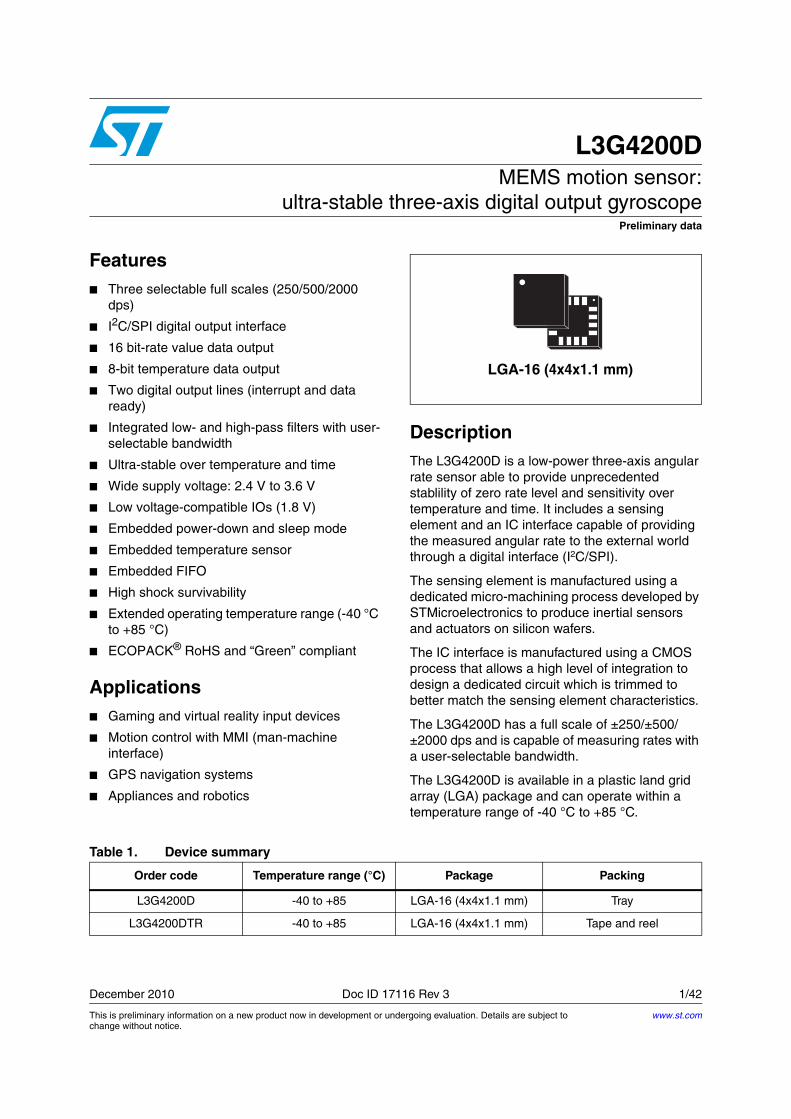
Preliminary data This is preliminary information on a new product now in development or undergoing evaluation. Details are subject to change without notice. December 2010 Doc ID 17116 Rev 3 1/42 42 L3G4200D MEMS motion sensor: ultra-stable three-axis digital output gyroscope Features ■ Three selectable full scales (250/500/2000 dps) ■ I 2 C/SPI digital output interface ■ 16 bit-rate value data output ■ 8-bit temperature data output ■ Two digital output lines (interrupt and data ready) ■ Integrated low- and high-pass filters with user- selectable bandwidth ■ Ultra-stable over temperature and time ■ Wide supply voltage: 2.4 V to 3.6 V ■ Low voltage-compatible IOs (1.8 V) ■ Embedded power-down and sleep mode ■ Embedded temperature sensor ■ Embedded FIFO ■ High shock survivability ■ Extended operating temperature range (-40 °C to +85 °C) ■ ECOPACK ® RoHS and “Green” compliant Applications ■ Gaming and virtual reality input devices ■ Motion control with MMI (man-machine interface) ■ GPS navigation systems ■ Appliances and robotics Description The L3G4200D is a low-power three-axis angular rate sensor able to provide unprecedented stablility of zero rate level and sensitivity over temperature and time. It includes a sensing element and an IC interface capable of providing the measured angular rate to the external world through a digital interface (I 2 C/SPI). The sensing element is manufactured using a dedicated micro-machining process developed by STMicroelectronics to produce inertial sensors and actuators on silicon wafers. The IC interface is manufactured using a CMOS process that allows a high level of integration to design a dedicated circuit which is trimmed to better match the sensing element characteristics. The L3G4200D has a full scale of ±250/±500/ ±2000 dps and is capable of measuring rates with a user-selectable bandwidth. The L3G4200D is available in a plastic land grid array (LGA) package and can operate within a temperature range of -40 °C to +85 °C. LGA-16 (4x4x1.1 mm) Table 1. Device summary Order code Temperature range (°C) Package Packing L3G4200D -40 to +85 LGA-16 (4x4x1.1 mm) Tray L3G4200DTR -40 to +85 LGA-16 (4x4x1.1 mm) Tape and reel www.st.com
Transcript of MEMS motion sensor: ultra-stable three-axis digital...
Preliminary data
This is preliminary information on a new product now in development or undergoing evaluation. Details are subject to change without notice.
December 2010 Doc ID 17116 Rev 3 1/42
42
L3G4200DMEMS motion sensor:
ultra-stable three-axis digital output gyroscope
Features Three selectable full scales (250/500/2000
dps)
I2C/SPI digital output interface
16 bit-rate value data output
8-bit temperature data output
Two digital output lines (interrupt and data ready)
Integrated low- and high-pass filters with user-selectable bandwidth
Ultra-stable over temperature and time
Wide supply voltage: 2.4 V to 3.6 V
Low voltage-compatible IOs (1.8 V)
Embedded power-down and sleep mode
Embedded temperature sensor
Embedded FIFO
High shock survivability
Extended operating temperature range (-40 °C to +85 °C)
ECOPACK® RoHS and “Green” compliant
Applications Gaming and virtual reality input devices
Motion control with MMI (man-machine interface)
GPS navigation systems
Appliances and robotics
DescriptionThe L3G4200D is a low-power three-axis angular rate sensor able to provide unprecedented stablility of zero rate level and sensitivity over temperature and time. It includes a sensing element and an IC interface capable of providing the measured angular rate to the external world through a digital interface (I2C/SPI).
The sensing element is manufactured using a dedicated micro-machining process developed by STMicroelectronics to produce inertial sensors and actuators on silicon wafers.
The IC interface is manufactured using a CMOS process that allows a high level of integration to design a dedicated circuit which is trimmed to better match the sensing element characteristics.
The L3G4200D has a full scale of ±250/±500/ ±2000 dps and is capable of measuring rates with a user-selectable bandwidth.
The L3G4200D is available in a plastic land grid array (LGA) package and can operate within a temperature range of -40 °C to +85 °C.
LGA-16 (4x4x1.1 mm)
Table 1. Device summary
Order code Temperature range (°C) Package Packing
L3G4200D -40 to +85 LGA-16 (4x4x1.1 mm) Tray
L3G4200DTR -40 to +85 LGA-16 (4x4x1.1 mm) Tape and reel
www.st.com
L3G4200D
2/42 Doc ID 17116 Rev 3
Contents
1 Block diagram and pin description . . . . . . . . . . . . . . . . . . . . . . . . . . . . . 7
1.1 Pin description . . . . . . . . . . . . . . . . . . . . . . . . . . . . . . . . . . . . . . . . . . . . . . 7
2 Mechanical and electrical characteristics . . . . . . . . . . . . . . . . . . . . . . . 10
2.1 Mechanical characteristics . . . . . . . . . . . . . . . . . . . . . . . . . . . . . . . . . . . . 10
2.2 Electrical characteristics . . . . . . . . . . . . . . . . . . . . . . . . . . . . . . . . . . . . . . 11
2.3 Temperature sensor characteristics . . . . . . . . . . . . . . . . . . . . . . . . . . . . . 11
2.4 Communication interface characteristics . . . . . . . . . . . . . . . . . . . . . . . . . 12
2.4.1 SPI - serial peripheral interface . . . . . . . . . . . . . . . . . . . . . . . . . . . . . . . 12
2.4.2 I2C - inter IC control interface . . . . . . . . . . . . . . . . . . . . . . . . . . . . . . . . 13
2.5 Absolute maximum ratings . . . . . . . . . . . . . . . . . . . . . . . . . . . . . . . . . . . . 14
2.6 Terminology . . . . . . . . . . . . . . . . . . . . . . . . . . . . . . . . . . . . . . . . . . . . . . . 15
2.6.1 Sensitivity . . . . . . . . . . . . . . . . . . . . . . . . . . . . . . . . . . . . . . . . . . . . . . . . 15
2.6.2 Zero-rate level . . . . . . . . . . . . . . . . . . . . . . . . . . . . . . . . . . . . . . . . . . . . 15
2.6.3 Self-test . . . . . . . . . . . . . . . . . . . . . . . . . . . . . . . . . . . . . . . . . . . . . . . . . 15
2.7 Soldering information . . . . . . . . . . . . . . . . . . . . . . . . . . . . . . . . . . . . . . . . 15
3 Main digital blocks . . . . . . . . . . . . . . . . . . . . . . . . . . . . . . . . . . . . . . . . . 16
3.1 Block diagram . . . . . . . . . . . . . . . . . . . . . . . . . . . . . . . . . . . . . . . . . . . . . . 16
3.2 FIFO . . . . . . . . . . . . . . . . . . . . . . . . . . . . . . . . . . . . . . . . . . . . . . . . . . . . . 16
3.2.1 Bypass mode . . . . . . . . . . . . . . . . . . . . . . . . . . . . . . . . . . . . . . . . . . . . . 16
3.2.2 FIFO mode . . . . . . . . . . . . . . . . . . . . . . . . . . . . . . . . . . . . . . . . . . . . . . . 17
3.2.3 Stream mode . . . . . . . . . . . . . . . . . . . . . . . . . . . . . . . . . . . . . . . . . . . . . 17
3.2.4 Bypass-to-stream mode . . . . . . . . . . . . . . . . . . . . . . . . . . . . . . . . . . . . . 18
3.2.5 Stream-to-FIFO mode . . . . . . . . . . . . . . . . . . . . . . . . . . . . . . . . . . . . . . 19
3.2.6 Retrieve data from FIFO . . . . . . . . . . . . . . . . . . . . . . . . . . . . . . . . . . . . 19
4 Application hints . . . . . . . . . . . . . . . . . . . . . . . . . . . . . . . . . . . . . . . . . . . 20
5 Digital interfaces . . . . . . . . . . . . . . . . . . . . . . . . . . . . . . . . . . . . . . . . . . . 21
5.1 I2C serial interface . . . . . . . . . . . . . . . . . . . . . . . . . . . . . . . . . . . . . . . . . . 21
5.1.1 I2C operation . . . . . . . . . . . . . . . . . . . . . . . . . . . . . . . . . . . . . . . . . . . . . 22
5.2 SPI bus interface . . . . . . . . . . . . . . . . . . . . . . . . . . . . . . . . . . . . . . . . . . . 23
5.2.1 SPI read . . . . . . . . . . . . . . . . . . . . . . . . . . . . . . . . . . . . . . . . . . . . . . . . . 24

L3G4200D
Doc ID 17116 Rev 3 3/42
5.2.2 SPI write . . . . . . . . . . . . . . . . . . . . . . . . . . . . . . . . . . . . . . . . . . . . . . . . 25
5.2.3 SPI read in 3-wire mode . . . . . . . . . . . . . . . . . . . . . . . . . . . . . . . . . . . . 26
6 Output register mapping . . . . . . . . . . . . . . . . . . . . . . . . . . . . . . . . . . . . 27
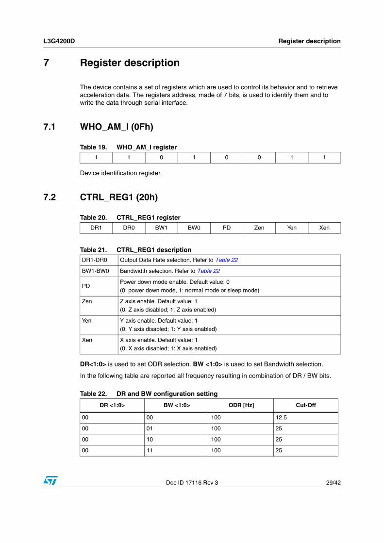
7 Register description . . . . . . . . . . . . . . . . . . . . . . . . . . . . . . . . . . . . . . . . 29
7.1 WHO_AM_I (0Fh) . . . . . . . . . . . . . . . . . . . . . . . . . . . . . . . . . . . . . . . . . . . 29
7.2 CTRL_REG1 (20h) . . . . . . . . . . . . . . . . . . . . . . . . . . . . . . . . . . . . . . . . . . 29
7.3 CTRL_REG2 (21h) . . . . . . . . . . . . . . . . . . . . . . . . . . . . . . . . . . . . . . . . . . 30
7.4 CTRL_REG3 (22h) . . . . . . . . . . . . . . . . . . . . . . . . . . . . . . . . . . . . . . . . . . 31
7.5 CTRL_REG4 (23h) . . . . . . . . . . . . . . . . . . . . . . . . . . . . . . . . . . . . . . . . . . 32
7.6 CTRL_REG5 (24h) . . . . . . . . . . . . . . . . . . . . . . . . . . . . . . . . . . . . . . . . . . 32
7.7 REFERENCE/DATACAPTURE (25h) . . . . . . . . . . . . . . . . . . . . . . . . . . . . 34
7.8 OUT_TEMP (26h) . . . . . . . . . . . . . . . . . . . . . . . . . . . . . . . . . . . . . . . . . . 34
7.9 STATUS_REG (27h) . . . . . . . . . . . . . . . . . . . . . . . . . . . . . . . . . . . . . . . . . 34
7.10 OUT_X_L (28h), OUT_X_H (29h) . . . . . . . . . . . . . . . . . . . . . . . . . . . . . . 35
7.11 OUT_Y_L (2Ah), OUT_Y_H (2Bh) . . . . . . . . . . . . . . . . . . . . . . . . . . . . . . 35
7.12 OUT_Z_L (2Ch), OUT_Z_H (2Dh) . . . . . . . . . . . . . . . . . . . . . . . . . . . . . . 35
7.13 FIFO_CTRL_REG (2Eh) . . . . . . . . . . . . . . . . . . . . . . . . . . . . . . . . . . . . . 35
7.14 FIFO_SRC_REG (2Fh) . . . . . . . . . . . . . . . . . . . . . . . . . . . . . . . . . . . . . . 35
7.15 INT1_CFG (30h) . . . . . . . . . . . . . . . . . . . . . . . . . . . . . . . . . . . . . . . . . . . . 36
7.16 INT1_SRC (31h) . . . . . . . . . . . . . . . . . . . . . . . . . . . . . . . . . . . . . . . . . . . . 36
7.17 INT1_THS_XH (32h) . . . . . . . . . . . . . . . . . . . . . . . . . . . . . . . . . . . . . . . . 37
7.18 INT1_THS_XL (33h) . . . . . . . . . . . . . . . . . . . . . . . . . . . . . . . . . . . . . . . . . 37
7.19 INT1_THS_YH (34h) . . . . . . . . . . . . . . . . . . . . . . . . . . . . . . . . . . . . . . . . 37
7.20 INT1_THS_YL (35h) . . . . . . . . . . . . . . . . . . . . . . . . . . . . . . . . . . . . . . . . . 38
7.21 INT1_THS_ZH (36h) . . . . . . . . . . . . . . . . . . . . . . . . . . . . . . . . . . . . . . . . 38
7.22 INT1_THS_ZL (37h) . . . . . . . . . . . . . . . . . . . . . . . . . . . . . . . . . . . . . . . . . 38
7.23 INT1_DURATION (38h) . . . . . . . . . . . . . . . . . . . . . . . . . . . . . . . . . . . . . . 38
8 Package information . . . . . . . . . . . . . . . . . . . . . . . . . . . . . . . . . . . . . . . . 40
9 Revision history . . . . . . . . . . . . . . . . . . . . . . . . . . . . . . . . . . . . . . . . . . . 41

List of tables L3G4200D
4/42 Doc ID 17116 Rev 3
List of tables
Table 1. Device summary . . . . . . . . . . . . . . . . . . . . . . . . . . . . . . . . . . . . . . . . . . . . . . . . . . . . . . . . . . 1Table 2. Pin description . . . . . . . . . . . . . . . . . . . . . . . . . . . . . . . . . . . . . . . . . . . . . . . . . . . . . . . . . . . 8Table 3. Filter values . . . . . . . . . . . . . . . . . . . . . . . . . . . . . . . . . . . . . . . . . . . . . . . . . . . . . . . . . . . . . 9Table 4. Mechanical characteristics @ Vdd = 3.0 V, T = 25 °C, unless otherwise noted . . . . . . . . . . . . 10
Table 5. Electrical characteristics @ Vdd =3.0 V, T=25 °C, unless otherwise noted . . . . . . . . . . . . . . . . 11
Table 6. Temp. sensor characteristics @ Vdd =3.0 V, T=25 °C, unless otherwise noted . . . . . . . . . . . 11
Table 7. SPI slave timing values. . . . . . . . . . . . . . . . . . . . . . . . . . . . . . . . . . . . . . . . . . . . . . . . . . . . 12Table 8. I2C slave timing values. . . . . . . . . . . . . . . . . . . . . . . . . . . . . . . . . . . . . . . . . . . . . . . . . . . . 13Table 9. Absolute maximum ratings . . . . . . . . . . . . . . . . . . . . . . . . . . . . . . . . . . . . . . . . . . . . . . . . . 14Table 10. PLL low-pass filter component values . . . . . . . . . . . . . . . . . . . . . . . . . . . . . . . . . . . . . . . . 20Table 11. Serial interface pin description . . . . . . . . . . . . . . . . . . . . . . . . . . . . . . . . . . . . . . . . . . . . . . 21Table 12. I2C terminology. . . . . . . . . . . . . . . . . . . . . . . . . . . . . . . . . . . . . . . . . . . . . . . . . . . . . . . . . . 21Table 13. SAD+read/write patterns. . . . . . . . . . . . . . . . . . . . . . . . . . . . . . . . . . . . . . . . . . . . . . . . . . . 22Table 14. Transfer when master is writing one byte to slave . . . . . . . . . . . . . . . . . . . . . . . . . . . . . . . 22Table 15. Transfer when master is writing multiple bytes to slave . . . . . . . . . . . . . . . . . . . . . . . . . . . 23Table 16. Transfer when master is receiving (reading) one byte of data from slave . . . . . . . . . . . . . 23Table 17. Transfer when master is receiving (reading) multiple bytes of data from slave . . . . . . . . . 23Table 18. Register address map. . . . . . . . . . . . . . . . . . . . . . . . . . . . . . . . . . . . . . . . . . . . . . . . . . . . . 27Table 19. WHO_AM_I register . . . . . . . . . . . . . . . . . . . . . . . . . . . . . . . . . . . . . . . . . . . . . . . . . . . . . . 29Table 20. CTRL_REG1 register . . . . . . . . . . . . . . . . . . . . . . . . . . . . . . . . . . . . . . . . . . . . . . . . . . . . . 29Table 21. CTRL_REG1 description . . . . . . . . . . . . . . . . . . . . . . . . . . . . . . . . . . . . . . . . . . . . . . . . . . 29Table 22. DR and BW configuration setting . . . . . . . . . . . . . . . . . . . . . . . . . . . . . . . . . . . . . . . . . . . . 29Table 23. Power mode selection configuration. . . . . . . . . . . . . . . . . . . . . . . . . . . . . . . . . . . . . . . . . . 30Table 24. CTRL_REG2 register . . . . . . . . . . . . . . . . . . . . . . . . . . . . . . . . . . . . . . . . . . . . . . . . . . . . . 30Table 25. CTRL_REG2 description . . . . . . . . . . . . . . . . . . . . . . . . . . . . . . . . . . . . . . . . . . . . . . . . . . 30Table 26. High pass filter mode configuration . . . . . . . . . . . . . . . . . . . . . . . . . . . . . . . . . . . . . . . . . . 31Table 27. High pass filter cut off frecuency configuration [Hz] . . . . . . . . . . . . . . . . . . . . . . . . . . . . . . 31Table 28. CTRL_REG1 register . . . . . . . . . . . . . . . . . . . . . . . . . . . . . . . . . . . . . . . . . . . . . . . . . . . . . 31Table 29. CTRL_REG3 description . . . . . . . . . . . . . . . . . . . . . . . . . . . . . . . . . . . . . . . . . . . . . . . . . . 31Table 30. CTRL_REG4 register . . . . . . . . . . . . . . . . . . . . . . . . . . . . . . . . . . . . . . . . . . . . . . . . . . . . . 32Table 31. CTRL_REG4 description . . . . . . . . . . . . . . . . . . . . . . . . . . . . . . . . . . . . . . . . . . . . . . . . . . 32Table 32. Self test mode configuration . . . . . . . . . . . . . . . . . . . . . . . . . . . . . . . . . . . . . . . . . . . . . . . . 32Table 33. CTRL_REG5 register . . . . . . . . . . . . . . . . . . . . . . . . . . . . . . . . . . . . . . . . . . . . . . . . . . . . . 32Table 34. CTRL_REG5 description . . . . . . . . . . . . . . . . . . . . . . . . . . . . . . . . . . . . . . . . . . . . . . . . . . 32Table 35. Out_Sel configuration setting . . . . . . . . . . . . . . . . . . . . . . . . . . . . . . . . . . . . . . . . . . . . . . . 33Table 36. INT_SEL configuration setting . . . . . . . . . . . . . . . . . . . . . . . . . . . . . . . . . . . . . . . . . . . . . . 33Table 37. REFERENCE register. . . . . . . . . . . . . . . . . . . . . . . . . . . . . . . . . . . . . . . . . . . . . . . . . . . . . 34Table 38. REFERENCE register description . . . . . . . . . . . . . . . . . . . . . . . . . . . . . . . . . . . . . . . . . . . 34Table 39. OUT_TEMP register . . . . . . . . . . . . . . . . . . . . . . . . . . . . . . . . . . . . . . . . . . . . . . . . . . . . . . 34Table 40. OUT_TEMP register description. . . . . . . . . . . . . . . . . . . . . . . . . . . . . . . . . . . . . . . . . . . . . 34Table 41. STATUS_REG register . . . . . . . . . . . . . . . . . . . . . . . . . . . . . . . . . . . . . . . . . . . . . . . . . . . . 34Table 42. STATUS_REG description . . . . . . . . . . . . . . . . . . . . . . . . . . . . . . . . . . . . . . . . . . . . . . . . . 34Table 43. REFERENCE register. . . . . . . . . . . . . . . . . . . . . . . . . . . . . . . . . . . . . . . . . . . . . . . . . . . . . 35Table 44. REFERENCE register description . . . . . . . . . . . . . . . . . . . . . . . . . . . . . . . . . . . . . . . . . . . 35Table 45. FIFO mode configuration . . . . . . . . . . . . . . . . . . . . . . . . . . . . . . . . . . . . . . . . . . . . . . . . . . 35Table 46. FIFO_SRC register . . . . . . . . . . . . . . . . . . . . . . . . . . . . . . . . . . . . . . . . . . . . . . . . . . . . . . . 35Table 47. FIFO_SRC register description. . . . . . . . . . . . . . . . . . . . . . . . . . . . . . . . . . . . . . . . . . . . . . 35Table 48. INT1_CFG register . . . . . . . . . . . . . . . . . . . . . . . . . . . . . . . . . . . . . . . . . . . . . . . . . . . . . . . 36

L3G4200D List of tables
Doc ID 17116 Rev 3 5/42
Table 49. INT1_CFG description . . . . . . . . . . . . . . . . . . . . . . . . . . . . . . . . . . . . . . . . . . . . . . . . . . . . 36Table 50. INT1_SRC register . . . . . . . . . . . . . . . . . . . . . . . . . . . . . . . . . . . . . . . . . . . . . . . . . . . . . . . 36Table 51. INT1_SRC description . . . . . . . . . . . . . . . . . . . . . . . . . . . . . . . . . . . . . . . . . . . . . . . . . . . . 37Table 52. INT1_THS_XH register . . . . . . . . . . . . . . . . . . . . . . . . . . . . . . . . . . . . . . . . . . . . . . . . . . . . 37Table 53. INT1_THS_XH description . . . . . . . . . . . . . . . . . . . . . . . . . . . . . . . . . . . . . . . . . . . . . . . . . 37Table 54. INT1_THS_XL register . . . . . . . . . . . . . . . . . . . . . . . . . . . . . . . . . . . . . . . . . . . . . . . . . . . . 37Table 55. INT1_THS_XL description . . . . . . . . . . . . . . . . . . . . . . . . . . . . . . . . . . . . . . . . . . . . . . . . . 37Table 56. INT1_THS_YH register . . . . . . . . . . . . . . . . . . . . . . . . . . . . . . . . . . . . . . . . . . . . . . . . . . . . 37Table 57. INT1_THS_YH description . . . . . . . . . . . . . . . . . . . . . . . . . . . . . . . . . . . . . . . . . . . . . . . . . 37Table 58. INT1_THS_YL register . . . . . . . . . . . . . . . . . . . . . . . . . . . . . . . . . . . . . . . . . . . . . . . . . . . . 38Table 59. INT1_THS_YL description . . . . . . . . . . . . . . . . . . . . . . . . . . . . . . . . . . . . . . . . . . . . . . . . . 38Table 60. INT1_THS_ZH register . . . . . . . . . . . . . . . . . . . . . . . . . . . . . . . . . . . . . . . . . . . . . . . . . . . . 38Table 61. INT1_THS_ZH description . . . . . . . . . . . . . . . . . . . . . . . . . . . . . . . . . . . . . . . . . . . . . . . . . 38Table 62. INT1_THS_ZL register . . . . . . . . . . . . . . . . . . . . . . . . . . . . . . . . . . . . . . . . . . . . . . . . . . . . 38Table 63. INT1_THS_ZL description . . . . . . . . . . . . . . . . . . . . . . . . . . . . . . . . . . . . . . . . . . . . . . . . . 38Table 64. INT1_DURATION register . . . . . . . . . . . . . . . . . . . . . . . . . . . . . . . . . . . . . . . . . . . . . . . . . 38Table 65. INT1_DURATION description. . . . . . . . . . . . . . . . . . . . . . . . . . . . . . . . . . . . . . . . . . . . . . . 38Table 66. Document revision history . . . . . . . . . . . . . . . . . . . . . . . . . . . . . . . . . . . . . . . . . . . . . . . . . 41
List of figures L3G4200D
6/42 Doc ID 17116 Rev 3
List of figures
Figure 1. Block diagram . . . . . . . . . . . . . . . . . . . . . . . . . . . . . . . . . . . . . . . . . . . . . . . . . . . . . . . . . . . . 7Figure 2. Pin connection . . . . . . . . . . . . . . . . . . . . . . . . . . . . . . . . . . . . . . . . . . . . . . . . . . . . . . . . . . . 7Figure 3. L3G4200D external low-pass filter values . . . . . . . . . . . . . . . . . . . . . . . . . . . . . . . . . . . . . . . . . . . . . . . . 8
Figure 4. SPI slave timing diagram . . . . . . . . . . . . . . . . . . . . . . . . . . . . . . . . . . . . . . . . . . . . . . . . . . 12Figure 5. I2C slave timing diagram . . . . . . . . . . . . . . . . . . . . . . . . . . . . . . . . . . . . . . . . . . . . . . . . . . 13Figure 6. Block diagram . . . . . . . . . . . . . . . . . . . . . . . . . . . . . . . . . . . . . . . . . . . . . . . . . . . . . . . . . . . 16Figure 7. Bypass mode . . . . . . . . . . . . . . . . . . . . . . . . . . . . . . . . . . . . . . . . . . . . . . . . . . . . . . . . . . . 17Figure 8. FIFO mode . . . . . . . . . . . . . . . . . . . . . . . . . . . . . . . . . . . . . . . . . . . . . . . . . . . . . . . . . . . . . 17Figure 9. Stream mode . . . . . . . . . . . . . . . . . . . . . . . . . . . . . . . . . . . . . . . . . . . . . . . . . . . . . . . . . . . 18Figure 10. Bypass-to-stream mode . . . . . . . . . . . . . . . . . . . . . . . . . . . . . . . . . . . . . . . . . . . . . . . . . . . 18Figure 11. Trigger stream mode . . . . . . . . . . . . . . . . . . . . . . . . . . . . . . . . . . . . . . . . . . . . . . . . . . . . . 19Figure 12. L3G4200D electrical connections and external component values . . . . . . . . . . . . . . . . . . 20Figure 13. Read and write protocol . . . . . . . . . . . . . . . . . . . . . . . . . . . . . . . . . . . . . . . . . . . . . . . . . . . 24Figure 14. SPI read protocol . . . . . . . . . . . . . . . . . . . . . . . . . . . . . . . . . . . . . . . . . . . . . . . . . . . . . . . . 24Figure 15. Multiple byte SPI read protocol (2-byte example) . . . . . . . . . . . . . . . . . . . . . . . . . . . . . . . . 25Figure 16. SPI write protocol . . . . . . . . . . . . . . . . . . . . . . . . . . . . . . . . . . . . . . . . . . . . . . . . . . . . . . . . 25Figure 17. Multiple byte SPI write protocol (2-byte example). . . . . . . . . . . . . . . . . . . . . . . . . . . . . . . . 26Figure 18. SPI read protocol in 3-wire mode . . . . . . . . . . . . . . . . . . . . . . . . . . . . . . . . . . . . . . . . . . . . 26Figure 19. INT1_Sel and Out_Sel configuration block diagram . . . . . . . . . . . . . . . . . . . . . . . . . . . . . 33Figure 20. Wait disabled . . . . . . . . . . . . . . . . . . . . . . . . . . . . . . . . . . . . . . . . . . . . . . . . . . . . . . . . . . . 39Figure 21. Wait enabled. . . . . . . . . . . . . . . . . . . . . . . . . . . . . . . . . . . . . . . . . . . . . . . . . . . . . . . . . . . . 39Figure 22. LGA-16: mechanical data and package dimensions . . . . . . . . . . . . . . . . . . . . . . . . . . . . . 40

L3G4200D Block diagram and pin description
Doc ID 17116 Rev 3 7/42
1 Block diagram and pin description
Figure 1. Block diagram
The vibration of the structure is maintained by drive circuitry in a feedback loop. The sensing signal is filtered and appears as a digital signal at the output.
1.1 Pin description
Figure 2. Pin connection
FIFOTRIMMINGCIRCUITSREFERENCE
MIXERCHARGEAMP
CLOCK
LOW-PASSFILTER
+ x,y,z
I2C
SPI
CSSCL/SPCSDA/SDO/SDISDO
Y+
Z+
Y-
Z-
X+
X-
DRIVING MASS
Feedback loop
MUX
A
D
DC
IGITAL
FILTERING
CONTROL LOGIC&
INTERRUPT GEN.
INT1
DRDY/INT2
ADC
TEMPERATURE
SENSOR
1
2
&PHASE GENERATOR
Ω
AM07225v1
(TOP VIEW)DIRECTIONS OF THE DETECTABLE ANGULAR RATES
1X
Vdd_IO
SCL/SPC
SDA/SDI/SDO
SDO/SA0
RES
RES
RES
RES
INT
DR
DY
/INT
2
CS
RE
S
PLLF
ILT
RE
S
Vdd
GN
D
1
8
12
5
49
13 16
+ΩZ
+ΩX
BOTTOM VIEW
+ΩY
AM07226v1

Block diagram and pin description L3G4200D
8/42 Doc ID 17116 Rev 3
Figure 3. L3G4200D external low-pass filter values (a)
Table 2. Pin description
Pin# Name Function
1 Vdd_IO Power supply for I/O pins
2SCL
SPC
I2C serial clock (SCL)
SPI serial port clock (SPC)
3
SDA
SDI
SDO
I2C serial data (SDA)
SPI serial data input (SDI)
3-wire interface serial data output (SDO)
4SDO
SA0
SPI serial data output (SDO)
I2C least significant bit of the device address (SA0)
5 CSSPI enable
I2C/SPI mode selection (1:SPI idle mode / I2C communication enabled; 0: SPI communication mode / I2C disabled)
6 DRDY/INT2 Data ready/FIFO interrupt
7 INT1 Programmable interrupt
8 Reserved Connect to GND
9 Reserved Connect to GND
10 Reserved Connect to GND
11 Reserved Connect to GND
12 Reserved Connect to GND
13 GND 0 V supply
14 PLLFILT Phase-locked loop filter (see Figure 3)
15 Reserved Connect to Vdd
16 Vdd Power supply
a. Pin 14 PLLFILT maximum voltage level is equal to Vdd.
L3G4200D Block diagram and pin description
Doc ID 17116 Rev 3 9/42
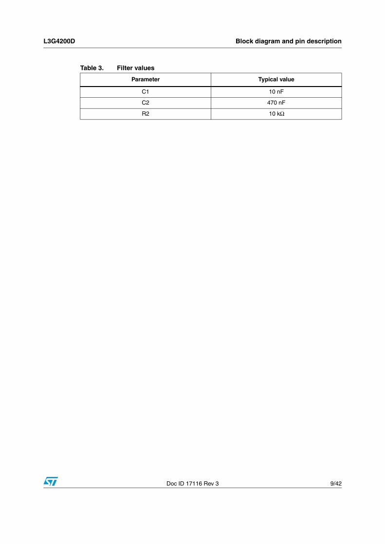
Table 3. Filter values
Parameter Typical value
C1 10 nF
C2 470 nF
R2 10 kΩ
Mechanical and electrical characteristics L3G4200D
10/42 Doc ID 17116 Rev 3
2 Mechanical and electrical characteristics
2.1 Mechanical characteristics
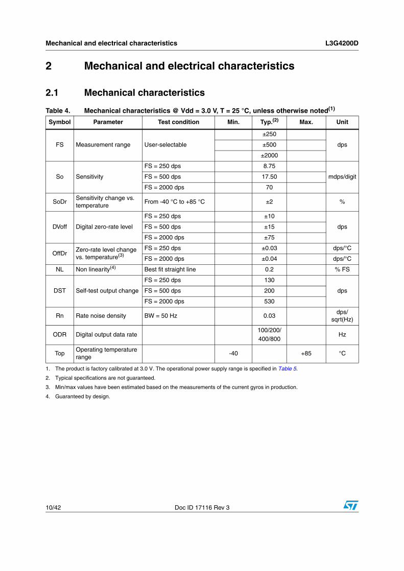
Table 4. Mechanical characteristics @ Vdd = 3.0 V, T = 25 °C, unless otherwise noted(1)
Symbol Parameter Test condition Min. Typ.(2) Max. Unit
FS Measurement range User-selectable
±250
dps±500
±2000
So Sensitivity
FS = 250 dps 8.75
mdps/digitFS = 500 dps 17.50
FS = 2000 dps 70
SoDrSensitivity change vs. temperature
From -40 °C to +85 °C ±2 %
DVoff Digital zero-rate level
FS = 250 dps ±10
dpsFS = 500 dps ±15
FS = 2000 dps ±75
OffDrZero-rate level change vs. temperature(3)
FS = 250 dps ±0.03 dps/°C
FS = 2000 dps ±0.04 dps/°C
NL Non linearity(4) Best fit straight line 0.2 % FS
DST Self-test output change
FS = 250 dps 130
dpsFS = 500 dps 200
FS = 2000 dps 530
Rn Rate noise density BW = 50 Hz 0.03dps/
sqrt(Hz)
ODR Digital output data rate100/200/400/800
Hz
Top Operating temperature range
-40 +85 °C
1. The product is factory calibrated at 3.0 V. The operational power supply range is specified in Table 5.
2. Typical specifications are not guaranteed.
3. Min/max values have been estimated based on the measurements of the current gyros in production.
4. Guaranteed by design.

L3G4200D Mechanical and electrical characteristics
Doc ID 17116 Rev 3 11/42
2.2 Electrical characteristics
2.3 Temperature sensor characteristics
Table 5. Electrical characteristics @ Vdd =3.0 V, T=25 °C, unless otherwise noted(1)
Symbol Parameter Test condition Min. Typ.(2) Max. Unit
Vdd Supply voltage 2.4 3.0 3.6 V
Vdd_IO I/O pins supply voltage(3) 1.71 Vdd+0.1 V
Idd Supply current 6.1 mA
IddSLSupply current
in sleep mode(4)Selectable by digital interface
1.5 mA
IddPdnSupply current in power-down mode
Selectable by digital interface
5 µA
Top Operating temperature range
-40 +85 °C
1. The product is factory calibrated at 3.0 V.
2. Typical specifications are not guaranteed.
3. It is possible to remove Vdd maintaining Vdd_IO without blocking the communication busses, in this condition the measurement chain is powered off.
4. Sleep mode introduces a faster turn-on time compared to power-down mode.
Table 6. Temp. sensor characteristics @ Vdd =3.0 V, T=25 °C, unless otherwise noted(1)
Symbol Parameter Test condition Min. Typ.(2) Max. Unit
TSDrTemperature sensor output change vs. temperature
-1 °C/digit
TODR Temperature refresh rate 1 Hz
Top Operating temperature range
-40 +85 °C
1. The product is factory calibrated at 3.0 V.
2. Typical specifications are not guaranteed.

Mechanical and electrical characteristics L3G4200D
12/42 Doc ID 17116 Rev 3
2.4 Communication interface characteristics
2.4.1 SPI - serial peripheral interface
Subject to general operating conditions for Vdd and Top.
Figure 4. SPI slave timing diagram(b)
Table 7. SPI slave timing values
Symbol ParameterValue(1)
UnitMin. Max.
tc(SPC) SPI clock cycle 100 ns
fc(SPC) SPI clock frequency 10 MHz
tsu(CS) CS setup time 5
ns
th(CS) CS hold time 8
tsu(SI) SDI input setup time 5
th(SI) SDI input hold time 15
tv(SO) SDO valid output time 50
th(SO) SDO output hold time 6
tdis(SO) SDO output disable time 50
1. Values are guaranteed at 10 MHz clock frequency for SPI with both 4 and 3 wires, based on characterization results; not tested in production.
b. Measurement points are done at 0.2·Vdd_IO and 0.8·Vdd_IO, for both input and output ports.

L3G4200D Mechanical and electrical characteristics
Doc ID 17116 Rev 3 13/42
2.4.2 I2C - inter IC control interface
Subject to general operating conditions for Vdd and Top.
Figure 5. I2C slave timing diagram (c)
Table 8. I2C slave timing values
Symbol ParameterI2C standard mode(1) I2C fast mode (1)
UnitMin Max Min Max
f(SCL) SCL clock frequency 0 100 0 400 kHz
tw(SCLL) SCL clock low time 4.7 1.3µs
tw(SCLH) SCL clock high time 4.0 0.6
tsu(SDA) SDA setup time 250 100 ns
th(SDA) SDA data hold time 0 3.45 0 0.9 µs
tr(SDA) tr(SCL) SDA and SCL rise time 1000 20 + 0.1Cb (2) 300
nstf(SDA) tf(SCL) SDA and SCL fall time 300 20 + 0.1Cb (2) 300
th(ST) START condition hold time 4 0.6
µs
tsu(SR)Repeated START condition setup time
4.7 0.6
tsu(SP) STOP condition setup time 4 0.6
tw(SP:SR)Bus free time between STOP and START condition
4.7 1.3
1. Data based on standard I2C protocol requirement; not tested in production.
2. Cb = total capacitance of one bus line, in pF.
c. Measurement points are done at 0.2·Vdd_IO and 0.8·Vdd_IO, for both ports.

Mechanical and electrical characteristics L3G4200D
14/42 Doc ID 17116 Rev 3
2.5 Absolute maximum ratingsAny stress above that listed as “Absolute maximum ratings” may cause permanent damage to the device. This is a stress rating only and functional operation of the device under these conditions is not implied. Exposure to maximum rating conditions for extended periods may affect device reliability.
Table 9. Absolute maximum ratings
Symbol Ratings Maximum value Unit
Vdd Supply voltage -0.3 to 4.8 V
TSTG Storage temperature range -40 to +125 °C
Sg Acceleration g for 0.1 ms 10,000 g
ESD Electrostatic discharge protection 2 (HBM) kV
This is a mechanical shock sensitive device, improper handling can cause permanent damage to the part
This is an ESD sensitive device, improper handling can cause permanent damage to the part

L3G4200D Mechanical and electrical characteristics
Doc ID 17116 Rev 3 15/42
2.6 Terminology
2.6.1 Sensitivity
An angular rate gyroscope is a device that produces a positive-going digital output for counterclockwise rotation around the sensitive axis considered. Sensitivity describes the gain of the sensor and can be determined by applying a defined angular velocity to it. This value changes very little over temperature and time.
2.6.2 Zero-rate level
Zero-rate level describes the actual output signal if there is no angular rate present. The zero-rate level of precise MEMS sensors is, to some extent, a result of stress to the sensor and, therefore, the zero-rate level can slightly change after mounting the sensor onto a printed circuit board or after exposing it to extensive mechanical stress. This value changes very little over temperature and time.
2.6.3 Stability over temperature and time
Thanks to the unique single driving mass approach and optimized design, ST gyroscopes are able to guarantee a perfect match of the MEMS mechanical mass and the ASIC interface, and deliver unprecedented levels of stability over temperature and time.
With Zero rate level and sensitivity performances, up to ten times better than equivalent products now available on the market, L3G4200D allows the user to avoid any further compensation and calibration during production for faster time to market, easy application implementation, higher performances and cost saving.
2.7 Soldering informationThe LGA package is compliant with the ECOPACK®, RoHS and “Green” standard. It is qualified for soldering heat resistance according to JEDEC J-STD-020.
Leave “pin 1 Indicator” unconnected during soldering.
Land pattern and soldering recommendations are available at www.st.com/.

Main digital blocks L3G4200D
16/42 Doc ID 17116 Rev 3
3 Main digital blocks
3.1 Block diagram
Figure 6. Block diagram
3.2 FIFOThe L3G4200D embeds a 32-slot, 16-bit data FIFO for each of the three output channels: yaw, pitch, and roll. This allows consistent power saving for the system, as the host processor does not need to continuously poll data from the sensor. Instead, it can wake up only when needed and burst the significant data out from the FIFO. This buffer can work in five different modes. Each mode is selected by the FIFO_MODE bits in the FIFO_CTRL_REG. Programmable watermark level, FIFO_empty or FIFO_Full events can be enabled to generate dedicated interrupts on the DRDY/INT2 pin (configured through CTRL_REG3), and event detection information is available in FIFO_SRC_REG. The watermark level can be configured to WTM4:0 in FIFO_CTRL_REG.
3.2.1 Bypass mode
In bypass mode, the FIFO is not operational and for this reason it remains empty. As illustrated in Figure 7, only the first address is used for each channel. The remaining FIFO slots are empty. When new data is available, the old data is overwritten.
L3G4200D Main digital blocks
Doc ID 17116 Rev 3 17/42
Figure 7. Bypass mode
3.2.2 FIFO mode
In FIFO mode, data from the yaw, pitch, and roll channels are stored in the FIFO. A watermark interrupt can be enabled (I2_WMK bit in CTRL_REG3), which is triggered when the FIFO is filled to the level specified in the WTM 4:0 bits of FIFO_CTRL_REG. The FIFO continues filling until it is full (32 slots of 16-bit data for yaw, pitch, and roll). When full, the FIFO stops collecting data from the input channels. To restart data collection, it is necessary to write FIFO_CTRL_REG back to bypass mode.
FIFO mode is represented in Figure 8.
Figure 8. FIFO mode
3.2.3 Stream mode
In stream mode, data from yaw, pitch, and roll measurements are stored in the FIFO. A watermark interrupt can be enabled and set as in FIFO mode. The FIFO continues filling until full (32 slots of 16-bit data for yaw, pitch, and roll). When full, the FIFO discards the

Main digital blocks L3G4200D
18/42 Doc ID 17116 Rev 3
older data as the new data arrives. Programmable watermark level events can be enabled to generate dedicated interrupts on the DRDY/INT2 pin (configured through CTRL_REG3).
Stream mode is represented in Figure 9.
Figure 9. Stream mode
3.2.4 Bypass-to-stream mode
In bypass-to-stream mode, the FIFO starts operating in bypass mode, and once a trigger event occurs (related to INT1_CFG register events), the FIFO starts operating in stream mode (see Figure 10).
Figure 10. Bypass-to-stream mode
L3G4200D Main digital blocks
Doc ID 17116 Rev 3 19/42
3.2.5 Stream-to-FIFO mode
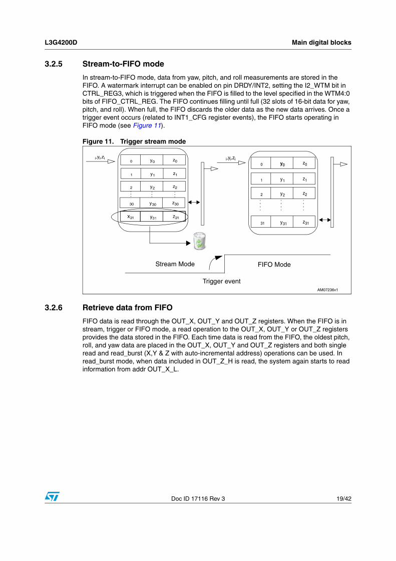
In stream-to-FIFO mode, data from yaw, pitch, and roll measurements are stored in the FIFO. A watermark interrupt can be enabled on pin DRDY/INT2, setting the I2_WTM bit in CTRL_REG3, which is triggered when the FIFO is filled to the level specified in the WTM4:0 bits of FIFO_CTRL_REG. The FIFO continues filling until full (32 slots of 16-bit data for yaw, pitch, and roll). When full, the FIFO discards the older data as the new data arrives. Once a trigger event occurs (related to INT1_CFG register events), the FIFO starts operating in FIFO mode (see Figure 11).
Figure 11. Trigger stream mode
3.2.6 Retrieve data from FIFO
FIFO data is read through the OUT_X, OUT_Y and OUT_Z registers. When the FIFO is in stream, trigger or FIFO mode, a read operation to the OUT_X, OUT_Y or OUT_Z registers provides the data stored in the FIFO. Each time data is read from the FIFO, the oldest pitch, roll, and yaw data are placed in the OUT_X, OUT_Y and OUT_Z registers and both single read and read_burst (X,Y & Z with auto-incremental address) operations can be used. In read_burst mode, when data included in OUT_Z_H is read, the system again starts to read information from addr OUT_X_L.

Application hints L3G4200D
20/42 Doc ID 17116 Rev 3
4 Application hints
Figure 12. L3G4200D electrical connections and external component values
Power supply decoupling capacitors (100 nF ceramic or polyester +10 µF) should be placed as near as possible to the device (common design practice).
If Vdd and Vdd_IO are not connected together, power supply decoupling capacitors (100 nF and 10 µF between Vdd and common ground, 100 nF between Vdd_IO and common ground) should be placed as near as possible to the device (common design practice).
The L3G4200D IC includes a PLL (phase locked loop) circuit to synchronize driving and sensing interfaces. Capacitors and resistors must be added at the PLLFILT pin (as shown in Figure 12) to implement a second-order low-pass filter. Table 10 summarizes the PLL low-pass filter component values.
Table 10. PLL low-pass filter component values
Component Value
C1 10 nF ± 10 %
C2 470 nF ± 10 %
R2 10 kΩ ± 10 %
100 nF
10kOhm 470nF
Vdd GND
C1
R2 C2
GND
10 µF
SCL/SPC
CS DR
SDO/SA0
SDA_SDI_SDO
10nF
Vdd_IO
PLL
FIL
T
Vdd
1
8
12
5
4 9
1316
TOPVIEW
PLL
FIL
T
GN
D
INT
GN
D
(TOP VIEW)DIRECTIONS OF THE DETECTABLE ANGULAR RATES
1X
+ΩZ
+ΩX
+ΩY
Vdd I2C bus
Rpu = 10kOhmRpu
SCL/SPC
SDA_SDI_SDO
Pull-up to be added when I2C interface is usedAM07949V1

L3G4200D Digital interfaces
Doc ID 17116 Rev 3 21/42
5 Digital interfaces
The registers embedded in the L3G4200D may be accessed through both the I2C and SPI serial interfaces. The latter may be software-configured to operate either in 3-wire or 4-wire interface mode.
The serial interfaces are mapped onto the same pins. To select/exploit the I2C interface, the CS line must be tied high (i.e., connected to Vdd_IO).
5.1 I2C serial interfaceThe L3G4200D I2C is a bus slave. The I2C is employed to write data to registers whose content can also be read back.
The relevant I2C terminology is given in the table below.
There are two signals associated with the I2C bus: the serial clock line (SCL) and the serial data line (SDA). The latter is a bidirectional line used for sending and receiving the data to/from the interface. Both lines must be connected to Vdd_IO through an external pull-up resistor. When the bus is free both the lines are high.
The I2C interface is compliant with fast mode (400 kHz) I2C standards as well as with normal mode.
Table 11. Serial interface pin description
Pin name Pin description
CSSPI enableI2C/SPI mode selection (1:SPI idle mode / I2C communication enabled; 0: SPI communication mode / I2C disabled)
SCL/SPCI2C serial clock (SCL)
SPI serial port clock (SPC)
SDA/SDI/SDO
I2C serial data (SDA)
SPI serial data input (SDI)
3-wire interface serial data output (SDO)
SDOSPI serial data output (SDO)
I2C least significant bit of the device address
Table 12. I2C terminology
Term Description
Transmitter The device which sends data to the bus
Receiver The device which receives data from the bus
MasterThe device which initiates a transfer, generates clock signals and terminates a transfer
Slave The device addressed by the master

Digital interfaces L3G4200D
22/42 Doc ID 17116 Rev 3
5.1.1 I2C operation
The transaction on the bus is started through a START (ST) signal. A START condition is defined as a HIGH to LOW transition on the data line while the SCL line is held HIGH. After this has been transmitted by the master, the bus is considered busy. The next byte of data transmitted after the start condition contains the address of the slave in the first 7 bits and the eighth bit tells whether the master is receiving data from the slave or transmitting data to the slave. When an address is sent, each device in the system compares the first 7 bits after a start condition with its address. If they match, the device considers itself addressed by the master.
The slave address (SAD) associated with the L3G4200D is 110100xb. The SDO pin can be used to modify the least significant bit (LSb) of the device address. If the SDO pin is connected to the voltage supply, LSb is ‘1’ (address 1101001b). Otherwise, if the SDO pin is connected to ground, the LSb value is ‘0’ (address 1101000b). This solution permits the connection and addressing of two different gyroscopes to the same I2C bus.
Data transfer with acknowledge is mandatory. The transmitter must release the SDA line during the acknowledge pulse. The receiver must then pull the data line LOW so that it remains stable low during the HIGH period of the acknowledge clock pulse. A receiver which has been addressed is obliged to generate an acknowledge after each byte of data received.
The I2C embedded in the L3G4200D behaves like a slave device, and the following protocol must be adhered to. After the START (ST) condition, a slave address is sent. Once a slave acknowledge (SAK) has been returned, an 8-bit sub-address is transmitted. The 7 LSb represent the actual register address while the MSB enables address auto-increment. If the MSb of the SUB field is 1, the SUB (register address) is automatically incremented to allow multiple data read/write.
The slave address is completed with a read/write bit. If the bit is ‘1’ (read), a REPEATED START (SR) condition must be issued after the two sub-address bytes; if the bit is ‘0’ (write) the master transmits to the slave with the direction unchanged. Table 13 describes how the SAD+read/write bit pattern is composed, listing all the possible configurations.
Table 13. SAD+read/write patterns
Command SAD[6:1] SAD[0] = SDO R/W SAD+R/W
Read 110100 0 1 11010001 (D1h)
Write 110100 0 0 11010000 (D0h)
Read 110100 1 1 11010011 (D3h)
Write 110100 1 0 11010010 (D2h)
Table 14. Transfer when master is writing one byte to slave
Master ST SAD + W SUB DATA SP
Slave SAK SAK SAK

L3G4200D Digital interfaces
Doc ID 17116 Rev 3 23/42
Data are transmitted in byte format (DATA). Each data transfer contains 8 bits. The number of bytes transferred per transfer is unlimited. Data is transferred with the most significant bit (MSb) first. If a receiver cannot receive another complete byte of data until it has performed some other function, it can hold the clock line SCL LOW to force the transmitter into a wait state. Data transfer only continues when the receiver is ready for another byte and releases the data line. If a slave receiver does not acknowledge the slave address (i.e., it is not able to receive because it is performing some real-time function) the data line must be left HIGH by the slave. The master can then abort the transfer. A LOW to HIGH transition on the SDA line while the SCL line is HIGH is defined as a STOP condition. Each data transfer must be terminated by the generation of a STOP (SP) condition.
In order to read multiple bytes, it is necessary to assert the most significant bit of the sub-address field. In other words, SUB(7) must be equal to 1, while SUB(6-0) represents the address of the first register to be read.
In the presented communication format, MAK is “master acknowledge” and NMAK is “no master acknowledge”.
5.2 SPI bus interfaceThe SPI is a bus slave. The SPI allows writing and reading of the device registers. The serial interface interacts with the external world through 4 wires: CS, SPC, SDI, and SDO.
Table 15. Transfer when master is writing multiple bytes to slave
Master ST SAD + W SUB DATA DATA SP
Slave SAK SAK SAK SAK
Table 16. Transfer when master is receiving (reading) one byte of data from slave
Master ST SAD + W SUB SR SAD + R NMAK SP
Slave SAK SAK SAK DATA
Table 17. Transfer when master is receiving (reading) multiple bytes of data from slave
Master ST SAD+W SUB SR SAD+R MAK MAK NMAK SP
Slave SAK SAK SAK DATA DATA DATA
Digital interfaces L3G4200D
24/42 Doc ID 17116 Rev 3
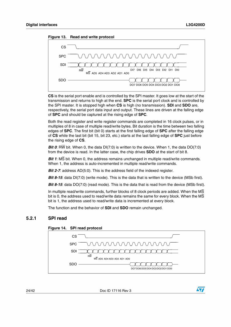
Figure 13. Read and write protocol
CS is the serial port enable and is controlled by the SPI master. It goes low at the start of the transmission and returns to high at the end. SPC is the serial port clock and is controlled by the SPI master. It is stopped high when CS is high (no transmission). SDI and SDO are, respectively, the serial port data input and output. These lines are driven at the falling edge of SPC and should be captured at the rising edge of SPC.
Both the read register and write register commands are completed in 16 clock pulses, or in multiples of 8 in case of multiple read/write bytes. Bit duration is the time between two falling edges of SPC. The first bit (bit 0) starts at the first falling edge of SPC after the falling edge of CS while the last bit (bit 15, bit 23, etc.) starts at the last falling edge of SPC just before the rising edge of CS.
Bit 0: RW bit. When 0, the data DI(7:0) is written to the device. When 1, the data DO(7:0) from the device is read. In the latter case, the chip drives SDO at the start of bit 8.
Bit 1: MS bit. When 0, the address remains unchanged in multiple read/write commands. When 1, the address is auto-incremented in multiple read/write commands.
Bit 2-7: address AD(5:0). This is the address field of the indexed register.
Bit 8-15: data DI(7:0) (write mode). This is the data that is written to the device (MSb first).
Bit 8-15: data DO(7:0) (read mode). This is the data that is read from the device (MSb first).
In multiple read/write commands, further blocks of 8 clock periods are added. When the MS bit is 0, the address used to read/write data remains the same for every block. When the MS bit is 1, the address used to read/write data is incremented at every block.
The function and the behavior of SDI and SDO remain unchanged.
5.2.1 SPI read
Figure 14. SPI read protocol
CS
SPC
SDI
SDO
RWAD5 AD4 AD3 AD2 AD1 AD0
DI7 DI6 DI5 DI4 DI3 DI2 DI1 DI0
DO7 DO6 DO5 DO4 DO3 DO2 DO1 DO0
MS
CS
SPC
SDI
SDO
RW
DO7 DO6 DO5 DO4 DO3 DO2 DO1 DO0
AD5 AD4 AD3 AD2 AD1 AD0MS

L3G4200D Digital interfaces
Doc ID 17116 Rev 3 25/42
The SPI read command is performed with 16 clock pulses. A multiple byte read command is performed by adding blocks of 8 clock pulses to the previous one.
Bit 0: READ bit. The value is 1.
Bit 1: MS bit. When 0, do not increment address; when 1, increment address in multiple reading.
Bit 2-7: address AD(5:0). This is the address field of the indexed register.
Bit 8-15: data DO(7:0) (read mode). This is the data that is read from the device (MSb first).
Bit 16-... : data DO(...-8). Further data in multiple byte reading.
Figure 15. Multiple byte SPI read protocol (2-byte example)
5.2.2 SPI write
Figure 16. SPI write protocol
The SPI write command is performed with 16 clock pulses. A multiple byte write command is performed by adding blocks of 8 clock pulses to the previous one.
Bit 0: WRITE bit. The value is 0.
Bit 1: MS bit. When 0, do not increment address; when 1, increment address in multiple writing.
Bit 2 -7: address AD(5:0). This is the address field of the indexed register.
Bit 8-15: data DI(7:0) (write mode). This is the data that is written to the device (MSb first).
Bit 16-... : data DI(...-8). Further data in multiple byte writing.
CS
SPC
SDI
SDO
RW
DO7 DO6 DO5 DO4 DO3 DO2 DO1 DO0
AD5 AD4 AD3 AD2 AD1 AD0
DO15 DO14 DO13 DO12 DO11 DO10 DO9 DO8
MS
CS
SPC
SDIRW DI7 DI6 DI5 DI4 DI3 DI2 DI1 DI0
AD5 AD4 AD3 AD2 AD1 AD0MS

Digital interfaces L3G4200D
26/42 Doc ID 17116 Rev 3
Figure 17. Multiple byte SPI write protocol (2-byte example)
5.2.3 SPI read in 3-wire mode
3-wire mode is entered by setting the SIM (SPI serial interface mode selection) bit to 1 in CTRL_REG2.
Figure 18. SPI read protocol in 3-wire mode
The SPI read command is performed with 16 clock pulses:
Bit 0: READ bit. The value is 1.
Bit 1: MS bit. When 0, do not increment address; when 1, increment address in multiple reading.
Bit 2-7: address AD(5:0). This is the address field of the indexed register.
Bit 8-15: data DO(7:0) (read mode). This is the data that is read from the device (MSb first).
The multiple read command is also available in 3-wire mode.
CS
SPC
SDI
RW
AD5 AD4 AD3 AD2 AD1 AD0
DI7 DI6 DI5 DI4 DI3 DI2 DI1 DI0 DI15 DI14 DI13 DI12 DI11 DI10 DI9 DI8
MS
CS
SPC
SDI/O
RW DO7 DO6 DO5 DO4 DO3 DO2 DO1 DO0
AD5 AD4 AD3 AD2 AD1 AD0MS

L3G4200D Output register mapping
Doc ID 17116 Rev 3 27/42
6 Output register mapping
The table given below provides a listing of the 8 bit registers embedded in the device and the related addresses:
Table 18. Register address map
Name TypeRegister address
Default CommentHex Binary
Reserved - 00-0E - -
WHO_AM_I r 0F 000 1111 11010011
Reserved - 10-1F - -
CTRL_REG1 rw 20 010 0000 00000111
CTRL_REG2 rw 21 010 0001 00000000
CTRL_REG3 rw 22 010 0010 00000000
CTRL_REG4 rw 23 010 0011 00000000
CTRL_REG5 rw 24 010 0100 00000000
REFERENCE rw 25 010 0101 00000000
OUT_TEMP r 26 010 0110 output
STATUS_REG r 27 010 0111 output
OUT_X_L r 28 010 1000 output
OUT_X_H r 29 010 1001 output
OUT_Y_L r 2A 010 1010 output
OUT_Y_H r 2B 010 1011 output
OUT_Z_L r 2C 010 1100 output
OUT_Z_H r 2D 010 1101 output
FIFO_CTRL_REG rw 2E 010 1110 00000000
FIFO_SRC_REG r 2F 010 1111 output
INT1_CFG rw 30 011 0000 00000000
INT1_SRC r 31 011 0001 output
INT1_TSH_XH rw 32 011 0010 00000000
INT1_TSH_XL rw 33 011 0011 00000000
INT1_TSH_YH rw 34 011 0100 00000000
INT1_TSH_YL rw 35 011 0101 00000000
INT1_TSH_ZH rw 36 011 0110 00000000
INT1_TSH_ZL rw 37 011 0111 00000000
INT1_DURATION rw 38 011 1000 00000000

Output register mapping L3G4200D
28/42 Doc ID 17116 Rev 3
Registers marked as Reserved must not be changed. The writing to those registers may cause permanent damages to the device.
The content of the registers that are loaded at boot should not be changed. They contain the factory calibration values. Their content is automatically restored when the device is powered-up.
L3G4200D Register description
Doc ID 17116 Rev 3 29/42
7 Register description
The device contains a set of registers which are used to control its behavior and to retrieve acceleration data. The registers address, made of 7 bits, is used to identify them and to write the data through serial interface.
7.1 WHO_AM_I (0Fh)
Device identification register.
7.2 CTRL_REG1 (20h)
DR<1:0> is used to set ODR selection. BW <1:0> is used to set Bandwidth selection.
In the following table are reported all frequency resulting in combination of DR / BW bits.
Table 19. WHO_AM_I register
1 1 0 1 0 0 1 1
Table 20. CTRL_REG1 register
DR1 DR0 BW1 BW0 PD Zen Yen Xen
Table 21. CTRL_REG1 description
DR1-DR0 Output Data Rate selection. Refer to Table 22
BW1-BW0 Bandwidth selection. Refer to Table 22
PDPower down mode enable. Default value: 0
(0: power down mode, 1: normal mode or sleep mode)
Zen Z axis enable. Default value: 1
(0: Z axis disabled; 1: Z axis enabled)
Yen Y axis enable. Default value: 1
(0: Y axis disabled; 1: Y axis enabled)
Xen X axis enable. Default value: 1
(0: X axis disabled; 1: X axis enabled)
Table 22. DR and BW configuration setting
DR <1:0> BW <1:0> ODR [Hz] Cut-Off
00 00 100 12.5
00 01 100 25
00 10 100 25
00 11 100 25

Register description L3G4200D
30/42 Doc ID 17116 Rev 3
Combination of PD, Zen, Yen, Xen are used to set device in different modes (power down / normal / sleep mode) according with the following table.
7.3 CTRL_REG2 (21h)
01 00 200 12.5
01 01 200 25
01 10 200 50
01 11 200 70
10 00 400 20
10 01 400 25
10 10 400 50
10 11 400 110
11 00 800 30
11 01 800 35
11 10 800 50
11 11 800 110
Table 23. Power mode selection configuration
Mode PD Zen Yen Xen
Power down 0 - - -
Sleep 1 0 0 0
Normal 1 - - -
Table 22. DR and BW configuration setting (continued)
DR <1:0> BW <1:0> ODR [Hz] Cut-Off
Table 24. CTRL_REG2 register
0(1)
1. Value loaded at boot. This value must not be changed
0(1) HPM1 HPM1 HPCF3 HPCF2 HPCF1 HPCF0
Table 25. CTRL_REG2 description
HPM1-HPM0
High Pass filter Mode Selection. Default value: 00Refer to Table 26
HPCF3-HPCF0
High Pass filter Cut Off frequency selectionRefer to Table 28

L3G4200D Register description
Doc ID 17116 Rev 3 31/42
7.4 CTRL_REG3 (22h)
Table 26. High pass filter mode configuration
HPM1 HPM0 High Pass filter Mode
0 0 Normal mode (reset reading HP_RESET_FILTER)
0 1 Reference signal for filtering
1 0 Normal mode
1 1 Autoreset on interrupt event
Table 27. High pass filter cut off frecuency configuration [Hz]
HPCF3 ODR= 100 Hz ODR= 200 Hz ODR= 400 Hz ODR= 800 Hz
0000 8 15 30 56
0001 4 8 15 30
0010 2 4 8 15
0011 1 2 4 8
0100 0.5 1 2 4
0101 0.2 0.5 1 2
0110 0.1 0.2 0.5 1
0111 0.05 0.1 0.2 0.5
1000 0.02 0.05 0.1 0.2
1001 0.01 0.02 0.05 0.1
Table 28. CTRL_REG1 register
I1_Int1 I1_Boot H_Lactive PP_OD I2_DRDY I2_WTM I2_ORun I2_Empty
Table 29. CTRL_REG3 description
I1_Int1 Interrupt enable on INT1 pin. Default value 0. (0: Disable; 1: Enable)
I1_Boot Boot status available on INT1. Default value 0. (0: Disable; 1: Enable)
H_Lactive Interrupt active configuration on INT1. Default value 0. (0: High; 1:Low)
PP_OD Push- Pull / Open drain. Default value: 0. (0: Push- Pull; 1: Open drain)
I2_DRDY Date Ready on DRDY/INT2. Default value 0. (0: Disable; 1: Enable)
I2_WTM FIFO Watermark interrupt on DRDY/INT2. Default value: 0. (0: Disable; 1: Enable)
I2_ORun FIFO Overrun interrupt on DRDY/INT2 Default value: 0. (0: Disable; 1: Enable)
I2_Empty FIFO Empty interrupt on DRDY/INT2. Default value: 0. (0: Disable; 1: Enable)
Register description L3G4200D
32/42 Doc ID 17116 Rev 3
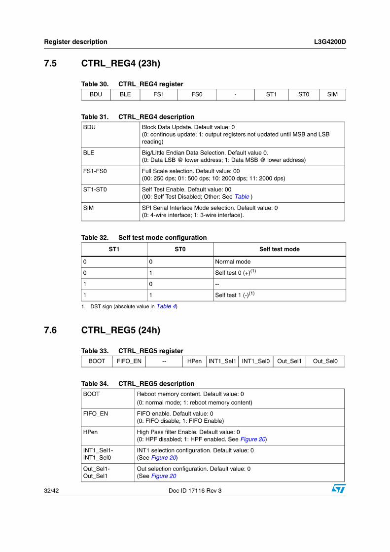
7.5 CTRL_REG4 (23h)
7.6 CTRL_REG5 (24h)
Table 30. CTRL_REG4 register
BDU BLE FS1 FS0 - ST1 ST0 SIM
Table 31. CTRL_REG4 description
BDU Block Data Update. Default value: 0(0: continous update; 1: output registers not updated until MSB and LSB reading)
BLE Big/Little Endian Data Selection. Default value 0.(0: Data LSB @ lower address; 1: Data MSB @ lower address)
FS1-FS0 Full Scale selection. Default value: 00(00: 250 dps; 01: 500 dps; 10: 2000 dps; 11: 2000 dps)
ST1-ST0 Self Test Enable. Default value: 00 (00: Self Test Disabled; Other: See Table )
SIM SPI Serial Interface Mode selection. Default value: 0 (0: 4-wire interface; 1: 3-wire interface).
Table 32. Self test mode configuration
ST1 ST0 Self test mode
0 0 Normal mode
0 1 Self test 0 (+)(1)
1. DST sign (absolute value in Table 4)
1 0 --
1 1 Self test 1 (-)(1)
Table 33. CTRL_REG5 register
BOOT FIFO_EN -- HPen INT1_Sel1 INT1_Sel0 Out_Sel1 Out_Sel0
Table 34. CTRL_REG5 description
BOOT Reboot memory content. Default value: 0
(0: normal mode; 1: reboot memory content)
FIFO_EN FIFO enable. Default value: 0(0: FIFO disable; 1: FIFO Enable)
HPen High Pass filter Enable. Default value: 0(0: HPF disabled; 1: HPF enabled. See Figure 20)
INT1_Sel1-INT1_Sel0
INT1 selection configuration. Default value: 0(See Figure 20)
Out_Sel1-Out_Sel1
Out selection configuration. Default value: 0(See Figure 20

L3G4200D Register description
Doc ID 17116 Rev 3 33/42
Figure 19. INT1_Sel and Out_Sel configuration block diagram
Table 35. Out_Sel configuration setting
Hpen OUT_SEL1 OUT_SEL0 Description
x 0 0Data in DataReg and FIFO are non-high-pass-filtered
x 0 1Data in DataReg and FIFO are high-pass-filtered
0 1 xData in DataReg and FIFO are low-pass-filtered by LPF2
1 1 xData in DataReg and FIFO are high-pass and low-pass-filtered by LPF2
Table 36. INT_SEL configuration setting
Hpen INT_SEL1 INT_SEL2 Description
x 0 0Non-high-pass-filtered data are used for interrupt generation
x 0 1High-pass-filtered data are used for interrupt generation
0 1 xLow-pass-filtered data are used for interrupt generation
1 1 xHigh-pass and low-pass-filtered data are used for interrupt generation
ADC LPF1 HPF
0
1
HPen
LPF2 10 11
01 00
Out_Sel <1:0>
DataReg
FIFO 32x16x3
00
11 10
01 Interrupt generator
INT1_Sel <1:0>
AM07949V2

Register description L3G4200D
34/42 Doc ID 17116 Rev 3
7.7 REFERENCE/DATACAPTURE (25h)
7.8 OUT_TEMP (26h)
7.9 STATUS_REG (27h)
Table 37. REFERENCE register
Ref7 Ref6 Ref5 Ref4 Ref3 Ref2 Ref1 Ref0
Table 38. REFERENCE register description
Ref 7-Ref0 Reference value for Interrupt generation. Default value: 0
Table 39. OUT_TEMP register
Temp7 Temp6 Temp5 Temp4 Temp3 Temp2 Temp1 Temp0
Table 40. OUT_TEMP register description
Temp7-Temp0 Temperature data.
Table 41. STATUS_REG register
ZYXOR ZOR YOR XOR ZYXDA ZDA YDA XDA
Table 42. STATUS_REG description
ZYXORX, Y, Z -axis data overrun. Default value: 0(0: no overrun has occurred; 1: new data has overwritten the previous one before it was read)
ZORZ axis data overrun. Default value: 0
(0: no overrun has occurred; 1: a new data for the Z-axis has overwritten the previous one)
YORY axis data overrun. Default value: 0
(0: no overrun has occurred; 1: a new data for the Y-axis has overwritten the previous one)
XORX axis data overrun. Default value: 0
(0: no overrun has occurred; 1: a new data for the X-axis has overwritten the previous one)
ZYXDA X, Y, Z -axis new data available. Default value: 0(0: a new set of data is not yet available; 1: a new set of data is available)
ZDA Z axis new data available. Default value: 0(0: a new data for the Z-axis is not yet available; 1: a new data for the Z-axis is available)
YDA Y axis new data available. Default value: 0(0: a new data for the Y-axis is not yet available;1: a new data for the Y-axis is available)
XDA X axis new data available. Default value: 0(0: a new data for the X-axis is not yet available; 1: a new data for the X-axis is available)

L3G4200D Register description
Doc ID 17116 Rev 3 35/42
7.10 OUT_X_L (28h), OUT_X_H (29h)X-axis angular rate data. The value is expressed as two’s complement.
7.11 OUT_Y_L (2Ah), OUT_Y_H (2Bh)Y-axis angular rate data. The value is expressed as two’s complement.
7.12 OUT_Z_L (2Ch), OUT_Z_H (2Dh)Z-axis angular rate data. The value is expressed as two’s complement.
7.13 FIFO_CTRL_REG (2Eh)
7.14 FIFO_SRC_REG (2Fh)
Table 43. REFERENCE register
FM2 FM1 FM0 WTM4 WTM3 WTM2 WTM1 WTM0
Table 44. REFERENCE register description
FM2-FM0 FIFO mode selection. Default value: 00 (see Table )
WTM4-WTM0 FIFO threshold. Watermark level setting
Table 45. FIFO mode configuration
FM2 FM1 FM0 FIFO mode
0 0 0 Bypass mode
0 0 1 FIFO mode
0 1 0 Stream mode
0 1 1 Stream-to-FIFO mode
1 0 0 Bypass-to-Stream mode
Table 46. FIFO_SRC register
WTM OVRN EMPTY FSS4 FSS3 FSS2 FSS1 FSS0
Table 47. FIFO_SRC register description
WTM Watermark status. (0: FIFO filling is lower than WTM level; 1: FIFO filling is equal or higher than WTM level)
OVRN Overrun bit status. (0: FIFO is not completely filled; 1:FIFO is completely filled)

Register description L3G4200D
36/42 Doc ID 17116 Rev 3
7.15 INT1_CFG (30h)
Configuration register for Interrupt source.
7.16 INT1_SRC (31h)
EMPTY FIFO empty bit. ( 0: FIFO not empty; 1: FIFO empty)
FSS4-FSS1 FIFO stored data level
Table 47. FIFO_SRC register description (continued)
Table 48. INT1_CFG register
AND/OR LIR ZHIE ZLIE YHIE YLIE XHIE XLIE
Table 49. INT1_CFG description
AND/ORAND/OR combination of Interrupt events. Default value: 0
(0: OR combination of interrupt events 1: AND combination of interrupt events
LIRLatch Interrupt Request. Default value: 0(0: interrupt request not latched; 1: interrupt request latched)Cleared by reading INT1_SRC reg.
ZHIEEnable interrupt generation on Z high event. Default value: 0
(0: disable interrupt request; 1: enable interrupt request on measured accel. value higher than preset threshold)
ZLIEEnable interrupt generation on Z low event. Default value: 0(0: disable interrupt request; 1: enable interrupt request on measured accel. value lower than preset threshold)
YHIEEnable interrupt generation on Y high event. Default value: 0
(0: disable interrupt request; 1: enable interrupt request on measured accel. value higher than preset threshold)
YLIEEnable interrupt generation on Y low event. Default value: 0
(0: disable interrupt request; 1: enable interrupt request on measured accel. value lower than preset threshold)
XHIEEnable interrupt generation on X high event. Default value: 0 (0: disable interrupt request; 1: enable interrupt request on measured accel. value higher than preset threshold)
XLIEEnable interrupt generation on X low event. Default value: 0
(0: disable interrupt request; 1: enable interrupt request on measured accel. value lower than preset threshold)
Table 50. INT1_SRC register
0 IA ZH ZL YH YL XH XL

L3G4200D Register description
Doc ID 17116 Rev 3 37/42
Interrupt source register. Read only register.
Reading at this address clears INT1_SRC IA bit (and eventually the interrupt signal on INT1 pin) and allows the refreshment of data in the INT1_SRC register if the latched option was chosen.
7.17 INT1_THS_XH (32h)
7.18 INT1_THS_XL (33h)
7.19 INT1_THS_YH (34h)
Table 51. INT1_SRC description
IAInterrupt active. Default value: 0
(0: no interrupt has been generated; 1: one or more interrupts have been generated)
ZH Z high. Default value: 0 (0: no interrupt, 1: Z High event has occurred)
ZL Z low. Default value: 0 (0: no interrupt; 1: Z Low event has occurred)
YH Y high. Default value: 0 (0: no interrupt, 1: Y High event has occurred)
YL Y low. Default value: 0 (0: no interrupt, 1: Y Low event has occurred)
XH X high. Default value: 0 (0: no interrupt, 1: X High event has occurred)
XL X low. Default value: 0 (0: no interrupt, 1: X Low event has occurred)
Table 52. INT1_THS_XH register
- THSX14 THSX13 THSX12 THSX11 THSX10 THSX9 THSX8
Table 53. INT1_THS_XH description
THSX14 - THSX9 Interrupt threshold. Default value: 0000 0000
Table 54. INT1_THS_XL register
THSX7 THSX6 THSX5 THSX4 THSX3 THSX2 THSX1 THSX0
Table 55. INT1_THS_XL description
THSX7 - THSX0 Interrupt threshold. Default value: 0000 0000
Table 56. INT1_THS_YH register
- THSY14 THSY13 THSY12 THSY11 THSY10 THSY9 THSY8
Table 57. INT1_THS_YH description
THSY14 - THSY9 Interrupt threshold. Default value: 0000 0000

Register description L3G4200D
38/42 Doc ID 17116 Rev 3
7.20 INT1_THS_YL (35h)
7.21 INT1_THS_ZH (36h)
7.22 INT1_THS_ZL (37h)
7.23 INT1_DURATION (38h)
D6 - D0 bits set the minimum duration of the Interrupt event to be recognized. Durationsteps and maximum values depend on the ODR chosen.
WAIT bit has the following meaning:
Wait =’0’: the interrupt falls immediately if signal crosses the selected threshold
Table 58. INT1_THS_YL register
THSR7 THSY6 THSY5 THSY4 THSY3 THSY2 THSY1 THSY0
Table 59. INT1_THS_YL description
THSY7 - THSY0 Interrupt threshold. Default value: 0000 0000
Table 60. INT1_THS_ZH register
- THSZ14 THSZ13 THSZ12 THSZ11 THSZ10 THSZ9 THSZ8
Table 61. INT1_THS_ZH description
THSZ14 - THSZ9 Interrupt threshold. Default value: 0000 0000
Table 62. INT1_THS_ZL register
THSZ7 THSZ6 THSZ5 THSZ4 THSZ3 THSZ2 THSZ1 THSZ0
Table 63. INT1_THS_ZL description
THSZ7 - THSZ0 Interrupt threshold. Default value: 0000 0000
Table 64. INT1_DURATION register
WAIT D6 D5 D4 D3 D2 D1 D0
Table 65. INT1_DURATION description
WAIT WAIT enable. Default value: 0 (0: disable; 1: enable)
D6 - D0 Duration value. Default value: 000 0000

L3G4200D Register description
Doc ID 17116 Rev 3 39/42
Wait =’1’: if signal crosses the selected threshold, the interrupt falls only after the duration has counted number of samples at the selected data rate, written into the duration counter register.
Figure 20. Wait disabled
Figure 21. Wait enabled

Package information L3G4200D
40/42 Doc ID 17116 Rev 3
8 Package information
In order to meet environmental requirements, ST offers these devices in different grades of ECOPACK® packages, depending on their level of environmental compliance. ECOPACK® specifications, grade definitions and product status are available at www.st.com. ECOPACK is an ST trademark.
Figure 22. LGA-16: mechanical data and package dimensions

L3G4200D Revision history
Doc ID 17116 Rev 3 41/42
9 Revision history
Table 66. Document revision history
Date Revision Changes
01-Apr-2010 1 Initial release.
03-Sep-2010 2 Complete datasheet review.
22-Dec-2010 3Inserted Section 6: Output register mapping and Section 7: Register description.

L3G4200D
42/42 Doc ID 17116 Rev 3
Please Read Carefully:
Information in this document is provided solely in connection with ST products. STMicroelectronics NV and its subsidiaries (“ST”) reserve theright to make changes, corrections, modifications or improvements, to this document, and the products and services described herein at anytime, without notice.
All ST products are sold pursuant to ST’s terms and conditions of sale.
Purchasers are solely responsible for the choice, selection and use of the ST products and services described herein, and ST assumes noliability whatsoever relating to the choice, selection or use of the ST products and services described herein.
No license, express or implied, by estoppel or otherwise, to any intellectual property rights is granted under this document. If any part of thisdocument refers to any third party products or services it shall not be deemed a license grant by ST for the use of such third party productsor services, or any intellectual property contained therein or considered as a warranty covering the use in any manner whatsoever of suchthird party products or services or any intellectual property contained therein.
UNLESS OTHERWISE SET FORTH IN ST’S TERMS AND CONDITIONS OF SALE ST DISCLAIMS ANY EXPRESS OR IMPLIEDWARRANTY WITH RESPECT TO THE USE AND/OR SALE OF ST PRODUCTS INCLUDING WITHOUT LIMITATION IMPLIEDWARRANTIES OF MERCHANTABILITY, FITNESS FOR A PARTICULAR PURPOSE (AND THEIR EQUIVALENTS UNDER THE LAWSOF ANY JURISDICTION), OR INFRINGEMENT OF ANY PATENT, COPYRIGHT OR OTHER INTELLECTUAL PROPERTY RIGHT.
UNLESS EXPRESSLY APPROVED IN WRITING BY AN AUTHORIZED ST REPRESENTATIVE, ST PRODUCTS ARE NOTRECOMMENDED, AUTHORIZED OR WARRANTED FOR USE IN MILITARY, AIR CRAFT, SPACE, LIFE SAVING, OR LIFE SUSTAININGAPPLICATIONS, NOR IN PRODUCTS OR SYSTEMS WHERE FAILURE OR MALFUNCTION MAY RESULT IN PERSONAL INJURY,DEATH, OR SEVERE PROPERTY OR ENVIRONMENTAL DAMAGE. ST PRODUCTS WHICH ARE NOT SPECIFIED AS "AUTOMOTIVEGRADE" MAY ONLY BE USED IN AUTOMOTIVE APPLICATIONS AT USER’S OWN RISK.
Resale of ST products with provisions different from the statements and/or technical features set forth in this document shall immediately voidany warranty granted by ST for the ST product or service described herein and shall not create or extend in any manner whatsoever, anyliability of ST.
ST and the ST logo are trademarks or registered trademarks of ST in various countries.
Information in this document supersedes and replaces all information previously supplied.
The ST logo is a registered trademark of STMicroelectronics. All other names are the property of their respective owners.
© 2010 STMicroelectronics - All rights reserved
STMicroelectronics group of companies
Australia - Belgium - Brazil - Canada - China - Czech Republic - Finland - France - Germany - Hong Kong - India - Israel - Italy - Japan - Malaysia - Malta - Morocco - Philippines - Singapore - Spain - Sweden - Switzerland - United Kingdom - United States of America
www.st.com