MEMS INERTIAL SENSOR 3-Axis - 2g/ · MEMS INERTIAL SENSOR 3-Axis - ±2g/±6g Digital Output Low...
42
Rev 1 October 2005 CD00047926 1/42 42 LIS3LV02DQ MEMS INERTIAL SENSOR 3-Axis - ±2g/±6g Digital Output Low Voltage Linear Accelerometer Features ■ 2.16V TO 3.6V SINGLE SUPPLY OPERATION ■ 1.8V COMPATIBLE IOs ■ I 2 C/SPI DIGITAL OUTPUT INTERFACES ■ PROGRAMMABLE 12 or 16 BIT DATA REPRESENTATION ■ INTERRUPT ACTIVATED BY MOTION ■ PROGRAMMABLE INTERRUPT THRESHOLD ■ EMBEDDED SELF TEST ■ HIGH SHOCK SURVIVABILITY ■ ECO-PACK COMPLIANT Description The LIS3LV02DQ is a three axes digital output linear accelerometer that includes a sensing element and an IC interface able to take the information from the sensing element and to provide the measured acceleration signals to the external world through an I 2 C/SPI serial interface. The sensing element, capable of detecting the acceleration, is manufactured using a dedicated process developed by ST to produce inertial sensors and actuators in silicon. The IC interface instead is manufactured using a CMOS process that allows high level of integration to design a dedicated circuit which is factory trimmed to better match the sensing element characteristics. The LIS3LV02DQ has a user selectable full scale of ±2g, ±6g and it is capable of measuring acceleration over a bandwidth of 640 Hz for all axes. The device bandwidth may be selected accordingly to the application requirements. A self-test capability allows the user to check the functioning of the system The device may be configured to generate an inertial wake-up/free-fall interrupt signal when a programmable acceleration threshold is crossed at least in one of the three axes. The LIS3LV02DQ is available in plastic SMD package and it is specified over a temperature range extending from -40°C to +85°C. The LIS3LV02DQ belongs to a family of products suitable for a variety of applications: ■ Free-Fall detection ■ Motion activated functions in portable terminals ■ Antitheft systems and Inertial navigation ■ Gaming and Virtual Reality input devices ■ Vibration Monitoring and Compensation QFPN-28 Order codes Part number Op. Temp. range, °C Package Packing LIS3LV02DQ -40 to +85 QFPN-28 Tray LIS3LV02DQ-TR -40 to +85 QFPN-28 Tape and Reel www.st.com
Transcript of MEMS INERTIAL SENSOR 3-Axis - 2g/ · MEMS INERTIAL SENSOR 3-Axis - ±2g/±6g Digital Output Low...

October 2005
LIS3LV02DQ
MEMS INERTIAL SENSOR3-Axis - ±2g/±6g Digital Output Low Voltage Linear Accelerometer
Features■ 2.16V TO 3.6V SINGLE SUPPLY
OPERATION
■ 1.8V COMPATIBLE IOs
■ I2C/SPI DIGITAL OUTPUT INTERFACES
■ PROGRAMMABLE 12 or 16 BIT DATA REPRESENTATION
■ INTERRUPT ACTIVATED BY MOTION
■ PROGRAMMABLE INTERRUPT THRESHOLD
■ EMBEDDED SELF TEST
■ HIGH SHOCK SURVIVABILITY
■ ECO-PACK COMPLIANT
DescriptionThe LIS3LV02DQ is a three axes digital outputlinear accelerometer that includes a sensingelement and an IC interface able to take theinformation from the sensing element and toprovide the measured acceleration signals to theexternal world through an I2C/SPI serial interface.
The sensing element, capable of detecting theacceleration, is manufactured using a dedicatedprocess developed by ST to produce inertialsensors and actuators in silicon.
The IC interface instead is manufactured using aCMOS process that allows high level of integrationto design a dedicated circuit which is factory
trimmed to better match the sensing elementcharacteristics.
The LIS3LV02DQ has a user selectable full scaleof ±2g, ±6g and it is capable of measuringacceleration over a bandwidth of 640 Hz for allaxes. The device bandwidth may be selectedaccordingly to the application requirements. Aself-test capability allows the user to check thefunctioning of the system
The device may be configured to generate aninertial wake-up/free-fall interrupt signal when aprogrammable acceleration threshold is crossedat least in one of the three axes.
The LIS3LV02DQ is available in plastic SMDpackage and it is specified over a temperaturerange extending from -40°C to +85°C.
The LIS3LV02DQ belongs to a family of productssuitable for a variety of applications:
■ Free-Fall detection
■ Motion activated functions in portable terminals
■ Antitheft systems and Inertial navigation
■ Gaming and Virtual Reality input devices
■ Vibration Monitoring and Compensation
QFPN-28
Order codesPart number Op. Temp. range, °C Package Packing
LIS3LV02DQ -40 to +85 QFPN-28 Tray
LIS3LV02DQ-TR -40 to +85 QFPN-28 Tape and Reel
Rev 1CD00047926 1/42
42www.st.com
LIS3LV02DQ
Contents
1 Block Diagram & Pin Description . . . . . . . . . . . . . . . . . . . . . . . . . . . . . . . . 5
1.1 Block diagram . . . . . . . . . . . . . . . . . . . . . . . . . . . . . . . . . . . . . . . . . . . . . . . . . 5
1.2 QFN Pin description . . . . . . . . . . . . . . . . . . . . . . . . . . . . . . . . . . . . . . . . . . . . 5
2 Mechanical and Electrical specifications . . . . . . . . . . . . . . . . . . . . . . . . . . 7
2.1 Mechanical characteristics1 . . . . . . . . . . . . . . . . . . . . . . . . . . . . . . . . . . . . . . 7
2.2 Electrical characteristics1 . . . . . . . . . . . . . . . . . . . . . . . . . . . . . . . . . . . . . . . 11
2.3 Absolute maximum ratings . . . . . . . . . . . . . . . . . . . . . . . . . . . . . . . . . . . . . . 12
2.4 Terminology . . . . . . . . . . . . . . . . . . . . . . . . . . . . . . . . . . . . . . . . . . . . . . . . . . 13
2.4.1 Sensitivity . . . . . . . . . . . . . . . . . . . . . . . . . . . . . . . . . . . . . . . . . . . . . . . . . . . 13
2.4.2 Zero-g level . . . . . . . . . . . . . . . . . . . . . . . . . . . . . . . . . . . . . . . . . . . . . . . . . . 13
2.4.3 Self Test . . . . . . . . . . . . . . . . . . . . . . . . . . . . . . . . . . . . . . . . . . . . . . . . . . . . . 13
3 Functionality . . . . . . . . . . . . . . . . . . . . . . . . . . . . . . . . . . . . . . . . . . . . . . . . 14
3.1 Sensing element . . . . . . . . . . . . . . . . . . . . . . . . . . . . . . . . . . . . . . . . . . . . . . 14
3.2 IC Interface . . . . . . . . . . . . . . . . . . . . . . . . . . . . . . . . . . . . . . . . . . . . . . . . . . 14
3.3 Factory calibration . . . . . . . . . . . . . . . . . . . . . . . . . . . . . . . . . . . . . . . . . . . . . 15
4 Application Hints . . . . . . . . . . . . . . . . . . . . . . . . . . . . . . . . . . . . . . . . . . . . . 16
4.1 Soldering Information . . . . . . . . . . . . . . . . . . . . . . . . . . . . . . . . . . . . . . . . . . 16
5 Digital Interfaces . . . . . . . . . . . . . . . . . . . . . . . . . . . . . . . . . . . . . . . . . . . . . 17
5.1 I2C Serial Interface . . . . . . . . . . . . . . . . . . . . . . . . . . . . . . . . . . . . . . . . . . . . 17
5.1.1 I2C Operation . . . . . . . . . . . . . . . . . . . . . . . . . . . . . . . . . . . . . . . . . . . . . . . . 18
5.2 SPI Bus Interface . . . . . . . . . . . . . . . . . . . . . . . . . . . . . . . . . . . . . . . . . . . . . 19
5.2.1 SPI Read . . . . . . . . . . . . . . . . . . . . . . . . . . . . . . . . . . . . . . . . . . . . . . . . . . . . 20
5.2.2 SPI Write . . . . . . . . . . . . . . . . . . . . . . . . . . . . . . . . . . . . . . . . . . . . . . . . . . . . 21
5.2.3 SPI Read in 3-wires mode . . . . . . . . . . . . . . . . . . . . . . . . . . . . . . . . . . . . . . . 21
6 Register mapping . . . . . . . . . . . . . . . . . . . . . . . . . . . . . . . . . . . . . . . . . . . . 23
7 Register Description . . . . . . . . . . . . . . . . . . . . . . . . . . . . . . . . . . . . . . . . . . 25
7.1 WHO_AM_I (0Fh) . . . . . . . . . . . . . . . . . . . . . . . . . . . . . . . . . . . . . . . . . . . . . 25
2/42 CD00047926

LIS3LV02DQ
7.2 OFFSET_X (16h) . . . . . . . . . . . . . . . . . . . . . . . . . . . . . . . . . . . . . . . . . . . . . 25
7.3 OFFSET_Y (17h) . . . . . . . . . . . . . . . . . . . . . . . . . . . . . . . . . . . . . . . . . . . . . 25
7.4 OFFSET_Z (18h) . . . . . . . . . . . . . . . . . . . . . . . . . . . . . . . . . . . . . . . . . . . . . 25
7.5 GAIN_X (19h) . . . . . . . . . . . . . . . . . . . . . . . . . . . . . . . . . . . . . . . . . . . . . . . . 26
7.6 GAIN_Y (1Ah) . . . . . . . . . . . . . . . . . . . . . . . . . . . . . . . . . . . . . . . . . . . . . . . . 26
7.7 GAIN_Z (1Bh) . . . . . . . . . . . . . . . . . . . . . . . . . . . . . . . . . . . . . . . . . . . . . . . . 26
7.8 CTRL_REG1 (20h) . . . . . . . . . . . . . . . . . . . . . . . . . . . . . . . . . . . . . . . . . . . . 26
7.9 CTRL_REG2 (21h) . . . . . . . . . . . . . . . . . . . . . . . . . . . . . . . . . . . . . . . . . . . . 27
7.10 CTRL_REG3 (22h) . . . . . . . . . . . . . . . . . . . . . . . . . . . . . . . . . . . . . . . . . . . . 28
7.11 HP_FILTER_RESET (23h) . . . . . . . . . . . . . . . . . . . . . . . . . . . . . . . . . . . . . . 29
7.12 STATUS_REG (27h) . . . . . . . . . . . . . . . . . . . . . . . . . . . . . . . . . . . . . . . . . . . 29
7.13 OUTX_L (28h) . . . . . . . . . . . . . . . . . . . . . . . . . . . . . . . . . . . . . . . . . . . . . . . . 29
7.14 OUTX_H (29h) . . . . . . . . . . . . . . . . . . . . . . . . . . . . . . . . . . . . . . . . . . . . . . . 29
7.15 OUTY_L (2Ah) . . . . . . . . . . . . . . . . . . . . . . . . . . . . . . . . . . . . . . . . . . . . . . . 30
7.16 OUTY_H (2Bh) . . . . . . . . . . . . . . . . . . . . . . . . . . . . . . . . . . . . . . . . . . . . . . . 30
7.17 OUTZ_L (2Ch) . . . . . . . . . . . . . . . . . . . . . . . . . . . . . . . . . . . . . . . . . . . . . . . 30
7.18 OUTZ_H (2Dh) . . . . . . . . . . . . . . . . . . . . . . . . . . . . . . . . . . . . . . . . . . . . . . . 30
7.19 FF_WU_CFG (30h) . . . . . . . . . . . . . . . . . . . . . . . . . . . . . . . . . . . . . . . . . . . . 31
7.20 FF_WU_SRC (31h) . . . . . . . . . . . . . . . . . . . . . . . . . . . . . . . . . . . . . . . . . . . . 32
7.21 FF_WU_ACK (32h) . . . . . . . . . . . . . . . . . . . . . . . . . . . . . . . . . . . . . . . . . . . . 32
7.22 FF_WU_THS_L (34h) . . . . . . . . . . . . . . . . . . . . . . . . . . . . . . . . . . . . . . . . . . 33
7.23 FF_WU_THS_H (35h) . . . . . . . . . . . . . . . . . . . . . . . . . . . . . . . . . . . . . . . . . 33
7.24 FF_WU_DURATION (36h) . . . . . . . . . . . . . . . . . . . . . . . . . . . . . . . . . . . . . . 33
7.25 DD_CFG (38h) . . . . . . . . . . . . . . . . . . . . . . . . . . . . . . . . . . . . . . . . . . . . . . . 34
7.26 DD_SRC (39h) . . . . . . . . . . . . . . . . . . . . . . . . . . . . . . . . . . . . . . . . . . . . . . . 35
7.27 DD_ACK (3Ah) . . . . . . . . . . . . . . . . . . . . . . . . . . . . . . . . . . . . . . . . . . . . . . . 35
7.28 DD_THSI_L (3Ch) . . . . . . . . . . . . . . . . . . . . . . . . . . . . . . . . . . . . . . . . . . . . . 36
7.29 DD_THSI_H (3Dh) . . . . . . . . . . . . . . . . . . . . . . . . . . . . . . . . . . . . . . . . . . . . 36
7.30 DD_THSE_L (3Eh) . . . . . . . . . . . . . . . . . . . . . . . . . . . . . . . . . . . . . . . . . . . . 36
7.31 DD_THSE_H (3Fh) . . . . . . . . . . . . . . . . . . . . . . . . . . . . . . . . . . . . . . . . . . . . 36
8 Typical performance characteristics . . . . . . . . . . . . . . . . . . . . . . . . . . . . . 37
8.1 Mechanical Characteristics at 25°C . . . . . . . . . . . . . . . . . . . . . . . . . . . . . . . 37
CD00047926 3/42

LIS3LV02DQ
8.2 Mechanical Characteristics derived from measurement in the-40°C to +85°C temperature range 38
8.3 Electro-Mechanical characteristics at 25°C . . . . . . . . . . . . . . . . . . . . . . . . . 39
9 Package Information . . . . . . . . . . . . . . . . . . . . . . . . . . . . . . . . . . . . . . . . . . 40
10 Revision history . . . . . . . . . . . . . . . . . . . . . . . . . . . . . . . . . . . . . . . . . . . . . . 41
4/42 CD00047926

LIS3LV02DQ 1 Block Diagram & Pin Description
1 Block Diagram & Pin Description
1.1 Block diagram
Figure 1. Block Diagram
1.2 QFPN-28 Pin description
Figure 2. Pin Connection
Σ∆CHARGEAMPLIFIER
MUX
Y+
Z+
Y-
Z-
Regsa
X+
X-
DEMUX
Reconstruction
Filter
Σ∆
Σ∆ Array
I2C
SPI
CS
SCL/SPC
SDA/SDO/SDI
SDO
CONTROL LOGIC&
INTERRUPT GEN.
RDY/INT
Reconstruction
Filter
Reconstruction
Filter
CLOCKTRIMMINGCIRCUITS
REFERENCESELF TEST
LIS3LV02DQ
NC
GND
Reserved
VDD
GND
RDY/INT
NC
NC
Reserved
Reserved
VDD
GND
CK
NC
NC
SD
O
VD
D_I
O
SD
A/S
DI/S
DO
SC
L/S
PC
CS
NC
NC
NC
NC
NC
NC
NC
NC
1
7
28 22
21
15
8 14
Y
1
X
Z
DIRECTION OF THEDETECTABLEACCELERATIONS
(TOP VIEW)
CD00047926 5/42

1 Block Diagram & Pin Description LIS3LV02DQ
Table 1. Pin description
Pin# Name Function
1 NC Internally not connected
2 GND 0V supply
3 Vdd Power supply
4 Reserved Either leave unconnected or connect to GND
5 GND 0V supply
6 RDY/INT Data ready/inertial wake-up and free-fall interrupt
7, 8 NC Internally not connected
9 SDO SPI Serial Data Output
10
SDA/
SDI/
SDO
I2C Serial Data (SDA)
SPI Serial Data Input (SDI)
3-wire Interface Serial Data Output (SDO)
11 Vdd_IO Power supply for I/O pads
12 SCL/SPCI2C Serial Clock (SCL)
SPI Serial Port Clock (SPC)
13 CSSPI enable
I2C/SPI mode selection (1: I2C mode; 0: SPI enabled)
14, 15 NC Internally not connected
16 CKOptional External clock, if not used either leave unconnected or connect to GND
17 GND 0V supply
18 Reserved Either leave unconnected or connect to Vdd_IO
19 Vdd Power supply
20 Reserved Connect to Vdd
21-28 NC Internally not connected
6/42 CD00047926

LIS3LV02DQ 2 Mechanical and Electrical specifications
2 Mechanical and Electrical specifications
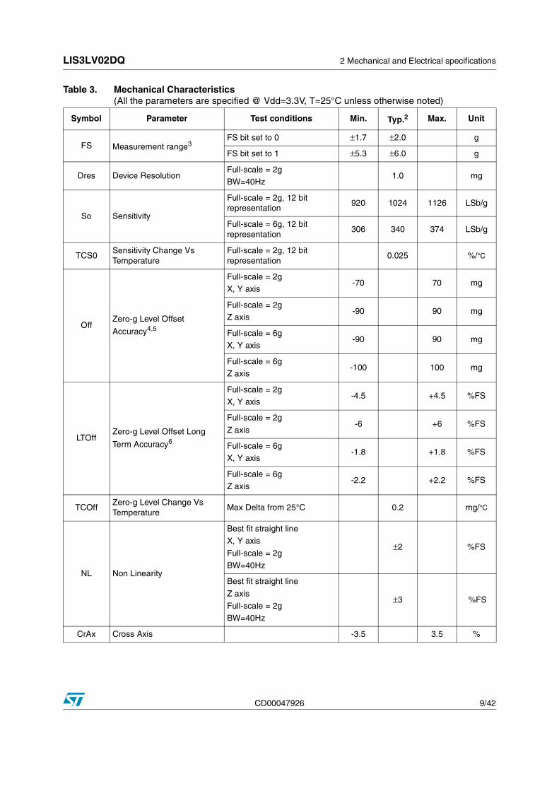
2.1 Mechanical characteristics1
Table 2. Mechanical Characteristics (All the parameters are specified @ Vdd=2.5V, T=25°C unless otherwise noted)
Symbol Parameter Test conditions Min. Typ.2 Max. Unit
FS Measurement range3FS bit set to 0 ±1.8 ±2.0 g
FS bit set to 1 ±5.6 ±6.0 g
Dres Device ResolutionFull-scale = 2g
BW=40Hz1.0 mg
So Sensitivity
Full-scale = 2g, 12 bit representation
974 1024 1074 LSb/g
Full-scale = 6g, 12 bit representation
323 340 357 LSb/g
TCS0Sensitivity Change Vs Temperature
Full-scale = 2g, 12 bit representation
0.025 %/°C
OffZero-g Level Offset
Accuracy4,5
Full-scale = 2g
X, Y axis-20 +20 mg
Full-scale = 2g
Z axis-40 +40 mg
Full-scale = 6g
X, Y axis-40 +40 mg
Full-scale = 6g
Z axis-60 +60 mg
LTOffZero-g Level Offset Long
Term Accuracy6
Full-scale = 2g
X, Y axis-2 +2 %FS
Full-scale = 2g
Z axis-5 +5 %FS
Full-scale = 6g
X, Y axis-1 +1 %FS
Full-scale = 6g
Z axis-2 +2 %FS
TCOffZero-g Level Change Vs Temperature
Max Delta from 25°C 0.2 mg/°C
CD00047926 7/42

2 Mechanical and Electrical specifications LIS3LV02DQ
Note: 1 The product is factory calibrated at 2.5V. The device can be used from 2.16V to 3.6V
2 Typical specifications are not guaranteed
3 Verified by wafer level test and measurement of initial offset and sensitivity
4 Zero-g level offset value after MSL3 preconditioning
5 Offset can be eliminated by enabling the built-in high pass filter (HPF)
6 Results of accelerated reliability tests. Report available upon request
7 Self Test output changes with the power supply. Self test “output change” is defined as OUTPUT[LSb](Self-test bit on ctrl_reg1=1)-OUTPUT[LSb](Self-test bit on ctrl_reg1=0). 1LSb=1g/1024 at 12bit representation, 2g Full-Scale
8 Output data reach 99% of final value after 5/ODR when enabling Self-Test mode due to device filtering
9 ODR is output data rate. Refer to table 4 for specifications
NL Non Linearity
Best fit straight line
X, Y axis
Full-scale = 2g
BW=40Hz
±2 %FS
Best fit straight line
Z axis
Full-scale = 2g
BW=40Hz
±3 %FS
CrAx Cross Axis -3.5 3.5 %
Vst Self test Output Change7,8
Full-scale=2g
X axis100 240 400 LSb
Full-scale=2g
Y axis100 240 400 LSb
Full-scale=2g
Z axis30 150 350 LSb
Full-scale=6g
X axis30 80 130 LSb
Full-scale=6g
Y axis30 80 130 LSb
Full-scale=6g
Z axis10 50 120 LSb
BW System Bandwidth9 ODRx/4 Hz
TopOperating Temperature Range
-40 +85 °C
Wh Product Weight 0.2 gram
Table 2. Mechanical Characteristics (continued)(All the parameters are specified @ Vdd=2.5V, T=25°C unless otherwise noted)
Symbol Parameter Test conditions Min. Typ.2 Max. Unit
8/42 CD00047926
LIS3LV02DQ 2 Mechanical and Electrical specifications
Table 3. Mechanical Characteristics (All the parameters are specified @ Vdd=3.3V, T=25°C unless otherwise noted)
Symbol Parameter Test conditions Min. Typ.2 Max. Unit
FS Measurement range3FS bit set to 0 ±1.7 ±2.0 g
FS bit set to 1 ±5.3 ±6.0 g
Dres Device ResolutionFull-scale = 2g
BW=40Hz1.0 mg
So Sensitivity
Full-scale = 2g, 12 bit representation
920 1024 1126 LSb/g
Full-scale = 6g, 12 bit representation
306 340 374 LSb/g
TCS0Sensitivity Change Vs Temperature
Full-scale = 2g, 12 bit representation
0.025 %/°C
OffZero-g Level Offset
Accuracy4,5
Full-scale = 2g
X, Y axis-70 70 mg
Full-scale = 2g
Z axis-90 90 mg
Full-scale = 6g
X, Y axis-90 90 mg
Full-scale = 6g
Z axis-100 100 mg
LTOffZero-g Level Offset Long
Term Accuracy6
Full-scale = 2g
X, Y axis-4.5 +4.5 %FS
Full-scale = 2g
Z axis-6 +6 %FS
Full-scale = 6g
X, Y axis-1.8 +1.8 %FS
Full-scale = 6g
Z axis-2.2 +2.2 %FS
TCOffZero-g Level Change Vs Temperature
Max Delta from 25°C 0.2 mg/°C
NL Non Linearity
Best fit straight line
X, Y axis
Full-scale = 2g
BW=40Hz
±2 %FS
Best fit straight line
Z axis
Full-scale = 2g
BW=40Hz
±3 %FS
CrAx Cross Axis -3.5 3.5 %
CD00047926 9/42

2 Mechanical and Electrical specifications LIS3LV02DQ
Note: 1 The product is factory calibrated at 2.5V. The device can be used from 2.16V to 3.6V
2 Typical specifications are not guaranteed
3 Verified by wafer level test and measurement of initial offset and sensitivity
4 Zero-g level offset value after MSL3 preconditioning
5 Offset can be eliminated by enabling the built-in high pass filter (HPF)
6 Results of accelerated reliability tests
7 Self Test output changes with the power supply. Self test “output change” is defined as OUTPUT[LSb](Self-test bit on ctrl_reg1=1)-OUTPUT[LSb](Self-test bit on ctrl_reg1=0). 1LSb=1g/1024 at 12bit representation, 2g Full-Scale
8 Output data reach 99% of final value after 5/ODR when enabling Self-Test mode due to device filtering
9 ODR is output data rate. Refer to table 4 for specifications
Vst Self test Output Change7,8
Full-scale=2g
X axis250 550 900 LSb
Full-scale=2g
Y axis250 550 900 LSb
Full-scale=2g
Z axis100 350 600 LSb
Full-scale=6g
X axis80 180 300 LSb
Full-scale=6g
Y axis80 180 300 LSb
Full-scale=6g
Z axis30 120 200 LSb
BW System Bandwidth9 ODRx/4 Hz
TopOperating Temperature Range
-40 +85 °C
Wh Product Weight 0.2 gram
Table 3. Mechanical Characteristics (continued)(All the parameters are specified @ Vdd=3.3V, T=25°C unless otherwise noted)
Symbol Parameter Test conditions Min. Typ.2 Max. Unit
10/42 CD00047926

LIS3LV02DQ 2 Mechanical and Electrical specifications
2.2 Electrical characteristics1
Note: 1 The product is factory calibrated at 2.5V. The device can be used from 2.16V to 3.6V
2 Typical specifications are not guaranteed
3 Digital filter cut-off frequency
4 Time to obtain valid data after exiting Power-Down mode
Table 4. Electrical Characteristics(All the parameters are specified @ Vdd=2.5V, T=25°C unless otherwise noted)
Symbol Parameter Test conditions Min. Typ.2 Max. Unit
Vdd Supply voltage 2.16 2.5 3.6 V
Vdd_IO I/O pads Supply voltage 1.71 Vdd V
Idd Supply currentT = 25°C, Vdd=2.5V 0.60 0.75 mA
T = 25°C, Vdd=3.3V 0.65 0.80 mA
VIHDigital High level Input voltage
0.8*Vdd_IO
V
VILDigital Low level Input voltage
0.2*Vdd_IO
V
VOH High level Output Voltage0.9*Vdd
_IOV
VOL Low level Output Voltage0.1*Vdd
_IOV
IddPdnCurrent consumption in Power-down mode
T = 25°C 1 10 µA
ODR1 Output Data Rate1 Dec factor = 512 40 Hz
ODR2 Output Data Rate 2 Dec factor = 128 160 Hz
ODR3 Output Data Rate 3 Dec factor = 32 640 Hz
ODR4 Output Data Rate 4 Dec factor = 8 2560 Hz
BW System Bandwidth3 ODRx/4 Hz
Ton Turn-on time4 5/ODRx s
TopOperating Temperature Range
-40 +85 °C
CD00047926 11/42

2 Mechanical and Electrical specifications LIS3LV02DQ
2.3 Absolute maximum ratings
Stresses above those listed as “absolute maximum ratings” may cause permanent damage to the device. This is a stress rating only and functional operation of the device under these conditions is not implied. Exposure to maximum rating conditions for extended periods may affect device reliability.
Table 5. Absolute maximum ratings
Note: 1 Supply voltage on any pin should never exceed 6.0V.
Symbol Ratings Maximum Value Unit
Vdd Supply voltage -0.3 to 6 V
Vdd_IO I/O pins Supply voltage -0.3 to Vdd +0.1 V
VinInput voltage on any control pin
(CS, SCL/SPC, SDA/SDI/SDO, CK) -0.3 to Vdd_IO +0.3 V
APOW Acceleration (Any axis, Powered, Vdd=2.5V)3000g for 0.5 ms
10000g for 0.1 ms
AUNP Acceleration (Any axis, Unpowered)3000g for 0.5 ms
10000g for 0.1 ms
TOP Operating Temperature Range -40 to +85 °C
TSTG Storage Temperature Range -40 to +125 °C
ESD Electrostatic discharge protection
4.0 (HBM) kV
200 (MM) V
1.5 (CDM) kV
This is a Mechanical Shock sensitive device, improper handling can cause permanent damages to the part
This is an ESD sensitive device, improper handling can cause permanent damages to the part
12/42 CD00047926

LIS3LV02DQ 2 Mechanical and Electrical specifications
2.4 Terminology
2.4.1 Sensitivity
Sensitivity describes the gain of the sensor and can be determined e.g. by applying 1gacceleration to it. As the sensor can measure DC accelerations this can be done easily bypointing the axis of interest towards the center of the earth, noting the output value, rotating thesensor by 180 degrees (point to the sky) and noting the output value again. By doing so, ±1gacceleration is applied to the sensor. Subtracting the larger output value from the smaller oneand divide the result by 2 leads to the actual sensitivity of the sensor. This value changes verylittle over temperature and also very little over time. The Sensitivity Tolerance describes therange of Sensitivities of a large population of sensor.
2.4.2 Zero-g level
Zero-g level Offset (Off) describes the deviation of an actual output signal from the ideal outputsignal if there is no acceleration present. A sensor in a steady state on a horizontal surface willmeasure 0g in X axis and 0g in Y axis whereas the Z axis will measure 1g. The output is ideallyin the middle of the dynamic range of the sensor (content of OUT registers 00h, 00h with 16 bitrepresentation, data expressed as 2’s complement number). A deviation from ideal value in thiscase is called Zero-g offset. Offset is to some extent a result of stress to a precise MEMSsensor and therefore the offset can slightly change after mounting the sensor onto a printedcircuit board or exposing it to extensive mechanical stress. Offset changes little overtemperature, see “Zero-g level change vs. temperature”. The Zero-g level of an individualsensor is stable over lifetime. The Zero-g level tolerance describes the range of Zero-g levels ofa population of sensors.
2.4.3 Self Test
Self Test allows to test the mechanical and electric part of the sensor, allowing the seismicmass to be moved by means of an electrostatic test-force. The Self Test function is off when theself-test bit of ctrl_reg1 (control register 1) is programmed to ‘0‘. When the self-test bit ofctrl_reg1 is programmed to ‘1‘ an actuation force is applied to the sensor, simulating a definiteinput acceleration. In this case the sensor outputs will exhibit a change in their DC levels whichis related to the selected full scale and depending on the Supply Voltage through the devicesensitivity. When Self Test is activated, the device output level is given by the algebraic sum ofthe signals produced by the acceleration acting on the sensor and by the electrostatic test-force. If the output signals change within the amplitude specified inside table 2 or table 3, thanthe sensor is working properly and the parameters of the interface chip are within the definedspecification.
CD00047926 13/42

3 Functionality LIS3LV02DQ
3 Functionality
The LIS3LV02DQ is a high performance, low-power, digital output 3-axis linear accelerometerpackaged in a QFN package. The complete device includes a sensing element and an ICinterface able to take the information from the sensing element and to provide a signal to theexternal world through an I2C/SPI serial interface.
3.1 Sensing element
A proprietary process is used to create a surface micro-machined accelerometer. Thetechnology allows to carry out suspended silicon structures which are attached to the substratein a few points called anchors and are free to move in the direction of the sensed acceleration.To be compatible with the traditional packaging techniques a cap is placed on top of thesensing element to avoid blocking the moving parts during the moulding phase of the plasticencapsulation.
When an acceleration is applied to the sensor the proof mass displaces from its nominalposition, causing an imbalance in the capacitive half-bridge. This imbalance is measured usingcharge integration in response to a voltage pulse applied to the sense capacitor.
At steady state the nominal value of the capacitors are few pF and when an acceleration isapplied the maximum variation of the capacitive load is up to 100fF.
3.2 IC Interface
The complete measurement chain is composed by a low-noise capacitive amplifier whichconverts into an analog voltage the capacitive unbalancing of the MEMS sensor and by threeΣ∆ analog-to-digital converters, one for each axis, that translate the produced signal into adigital bitstream.
The Σ∆ converters are coupled with dedicated reconstruction filters which remove the highfrequency components of the quantization noise and provide low rate and high resolution digitalwords.
The charge amplifier and the Σ∆ converters are operated respectively at 61.5 kHz and 20.5kHz.
The data rate at the output of the reconstruction depends on the user selected DecimationFactor (DF) and spans from 40 Hz to 2560 Hz.
The acceleration data may be accessed through an I2C/SPI interface thus making the deviceparticularly suitable for direct interfacing with a microcontroller.
The LIS3LV02DQ features a Data-Ready signal (RDY) which indicates when a new set ofmeasured acceleration data is available thus simplifying data synchronization in digital systememploying the device itself.
The LIS3LV02DQ may also be configured to generate an inertial Wake-Up, Direction Detectionand Free-Fall interrupt signal accordingly to a programmed acceleration event along theenabled axes.
14/42 CD00047926

LIS3LV02DQ 3 Functionality
3.3 Factory calibration
The IC interface is factory calibrated for sensitivity (So) and Zero-g level (Off).
The trimming values are stored inside the device by a non volatile structure. Any time thedevice is turned on, the trimming parameters are downloaded into the registers to be employedduring the normal operation. This allows the user to employ the device without furthercalibration.
CD00047926 15/42

4 Application Hints LIS3LV02DQ
4 Application Hints
Figure 3. LIS3LV02DQ Electrical Connection
The device core is supplied through Vdd line while the I/O pads are supplied through Vdd_IO line. Power supply decoupling capacitors (100 nF ceramic, 10 µF Al) should be placed as near as possible to the pin 3 of the device (common design practice).
All the voltage and ground supplies must be present at the same time to have proper behavior of the IC (refer to Fig. 3). It is possible to remove Vdd mantaining Vdd_IO without blocking the communication busses.
The functionality of the device and the measured acceleration data is selectable and accessible through the I2C/SPI interface.When using the I2C, CS must be tied high while SDO must be left floating. Refer to application note AN2041 for further information on device usage.
4.1 Soldering Information
The QFN-28 package is lead free and green package qualified for soldering heat resistance according to JEDEC J-STD-020C. Central die pad and pin #1 indicator are physically connected to GND. Land pattern and soldering recommendations are available upon request.
LIS3LV02DQ
1
7
28 22
21
15
8 14DIRECTION OF THEDETECTABLEACCELERATIONS
Vdd_IO
CS
SC
L/S
PC
SD
A/S
DI/S
DO
SD
O
RD
Y/IN
T
10uF
Vdd
Digital signal from/to signal controller.Signal’s levels are defined by proper selection of Vdd_IO
100nF
GND
(TOP VIEW)
Y
1
X
Z
16/42 CD00047926

LIS3LV02DQ 5 Digital Interfaces
5 Digital Interfaces
The registers embedded inside the LIS3LV02DQ may be accessed through both the I2C and SPI serial interfaces. The latter may be SW configured to operate either in 3-wire or 4-wire interface mode.
The serial interfaces are mapped onto the same pads. To select/exploit the I2C interface, CS line must be tied high (i.e connected to Vdd_IO).
Table 6. Serial interface pin description
5.1 I2C Serial Interface
The LIS3LV02DQ I2C is a bus slave. The I2C is employed to write the data into the registers whose content can also be read back.
The relevant I2C terminology is given in the table below
Table 7. Serial interface pin description
There are two signals associated with the I2C bus: the Serial Clock Line (SCL) and the Serial DAta line (SDA). The latter is a bidirectional line used for sending and receiving the data to/from the interface. Both the lines are connected to Vdd_IO through a pull-up resistor embedded inside the LIS3LV02DQ. When the bus is free both the lines are high.
The I2C interface is compliant with Fast Mode (400 kHz) I2C standards as well as the Normal Mode.
PIN Name PIN Description
CSSPI enable
I2C/SPI mode selection (1: I2C mode; 0: SPI enabled)
SCL/SPCI2C Serial Clock (SCL)
SPI Serial Port Clock (SPC)
SDA/SDI/SDOI2C Serial Data (SDA)
SPI Serial Data Input (SDI)
3-wire Interface Serial Data Output (SDO)
SDO SPI Serial Data Output (SDO)
Term Description
Transmitter The device which sends data to the bus
Receiver The device which receives data from the bus
MasterThe device which initiates a transfer, generates clock signals and terminates a transfer
Slave The device addressed by the master
CD00047926 17/42
5 Digital Interfaces LIS3LV02DQ
5.1.1 I2C Operation
The transaction on the bus is started through a START (ST) signal. A START condition is defined as a HIGH to LOW transition on the data line while the SCL line is held HIGH. After this has been transmitted by the Master, the bus is considered busy. The next byte of data transmitted after the start condition contains the address of the slave in the first 7 bits and the eighth bit tells whether the Master is receiving data from the slave or transmitting data to the slave. When an address is sent, each device in the system compares the first seven bits after a start condition with its address. If they match, the device considers itself addressed by the Master. The Slave ADdress (SAD) associated to the LIS3LV02DQ is 0011101b.
Data transfer with acknowledge is mandatory. The transmitter must release the SDA line during the acknowledge pulse. The receiver must then pull the data line LOW so that it remains stable low during the HIGH period of the acknowledge clock pulse. A receiver which has been addressed is obliged to generate an acknowledge after each byte of data has been received.
The I2C embedded inside the LIS3LV02DQ behaves like a slave device and the following protocol must be adhered to. After the start condition (ST) a salve address is sent, once a slave acknowledge (SAK) has been returned, a 8-bit sub-address will be transmitted: the 7 LSb represent the actual register address while the MSB enables address auto increment. If the MSb of the SUB field is 1, the SUB (register address) will be automatically incremented to allow multiple data read/write.
The slave address is completed with a Read/Write bit. If the bit was ‘1’ (Read), a repeated START (SR) condition will have to be issued after the two sub-address bytes; if the bit is ‘0’ (Write) the Master will transmit to the slave with direction unchanged.
Transfer when Master is writing one byte to slave
Transfer when Master is writing multiple bytes to slave:
Transfer when Master is receiving (reading) one byte of data from slave:
Transfer when Master is receiving (reading) multiple bytes of data from slave
Data are transmitted in byte format (DATA). Each data transfer contains 8 bits. The number of bytes transferred per transfer is unlimited. Data is transferred with the Most Significant bit (MSb) first. If a receiver can’t receive another complete byte of data until it has performed some other
Master ST SAD + W SUB DATA SP
Slave SAK SAK SAK
Master ST SAD + W SUB DATA DATA SP
Slave SAK SAK SAK SAK
Master ST SAD + W SUB SR SAD + R NMAK SP
Slave SAK SAK SAK DATA
Master ST SAD + W SUB SR SAD + R MAK
Slave SAK SAK SAK DATA
Master MAK NMAK SP
Slave DATA DATA
18/42 CD00047926

LIS3LV02DQ 5 Digital Interfaces
function, it can hold the clock line, SCL LOW to force the transmitter into a wait state. Data transfer only continues when the receiver is ready for another byte and releases the data line. If a slave receiver doesn’t acknowledge the slave address (i.e. it is not able to receive because it is performing some real time function) the data line must be left HIGH by the slave. The Master can then abort the transfer. A LOW to HIGH transition on the SDA line while the SCL line is HIGH is defined as a STOP condition. Each data transfer must be terminated by the generation of a STOP (SP) condition.
In order to read multiple bytes, it is necessary to assert the most significant bit of the sub-address field. In other words, SUB(7) must be equal to 1 while SUB(6-0) represents the address of first register to read.
In the presented communication format MAK is Master Acknowledge and NMAK is No Master Acknowledge.
5.2 SPI Bus Interface
The LIS3LV02DQ SPI is a bus slave. The SPI allows to write and read the registers of the device.
The Serial Interface interacts with the outside world with 4 wires: CS, SPC, SDI and SDO.
Figure 4. Read & write protocol
CS is the Serial Port Enable and it is controlled by the SPI master. It goes low at the start of the transmission and goes back high at the end. SPC is the Serial Port Clock and it is controlled by the SPI master. It is stopped high when CS is high (no transmission). SDI and SDO are respectively the Serial Port Data Input and Output. Those lines are driven at the falling edge of SPC and should be captured at the rising edge of SPC.
Both the Read Register and Write Register commands are completed in 16 clock pulses or in multiple of 8 in case of multiple byte read/write. Bit duration is the time between two falling edges of SPC. The first bit (bit 0) starts at the first falling edge of SPC after the falling edge of CS while the last bit (bit 15, bit 23, ...) starts at the last falling edge of SPC just before the rising edge of CS.
bit 0: RW bit. When 0, the data DI(7:0) is written into the device. When 1, the data DO(7:0) from the device is read. In latter case, the chip will drive SDO at the start of bit 8.
bit 1: MS bit. When 0, the address will remain unchanged in multiple read/write commands. When 1, the address will be auto incremented in multiple read/write commands.
bit 2-7: address AD(5:0). This is the address field of the indexed register.
CS
SPC
SDI
SDO
RWAD5 AD4 AD3 AD2 AD1 AD0
DI7 DI6 DI5 DI4 DI3 DI2 DI1 DI0
DO7 DO6 DO5 DO4 DO3 DO2 DO1 DO0
MS
CD00047926 19/42
5 Digital Interfaces LIS3LV02DQ
bit 8-15: data DI(7:0) (write mode). This is the data that will be written into the device (MSb first).
bit 8-15: data DO(7:0) (read mode). This is the data that will be read from the device (MSb first).
In multiple read/write commands further blocks of 8 clock periods will be added. When MS bit is 0 the address used to read/write data remains the same for every block. When MS bit is 1 the address used to read/write data is incremented at every block.
The function and the behavior of SDI and SDO remain unchanged.
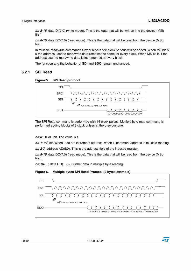
5.2.1 SPI Read
Figure 5. SPI Read protocol
The SPI Read command is performed with 16 clock pulses. Multiple byte read command is performed adding blocks of 8 clock pulses at the previous one.
bit 0: READ bit. The value is 1.
bit 1: MS bit. When 0 do not increment address, when 1 increment address in multiple reading.
bit 2-7: address AD(5:0). This is the address field of the indexed register.
bit 8-15: data DO(7:0) (read mode). This is the data that will be read from the device (MSb first).
bit 16-... : data DO(...-8). Further data in multiple byte reading.
Figure 6. Multiple bytes SPI Read Protocol (2 bytes example)
CS
SPC
SDI
SDO
RW
DO7 DO6 DO5 DO4 DO3 DO2DO1 DO0
AD5 AD4 AD3 AD2 AD1 AD0MS
CS
SPC
SDI
SDO
RW
DO7 DO6 DO5 DO4 DO3 DO2 DO1 DO0
AD5 AD4 AD3 AD2 AD1 AD0
DO15 DO14 DO13 DO12 DO11 DO10 DO9 DO8
MS
20/42 CD00047926

LIS3LV02DQ 5 Digital Interfaces
5.2.2 SPI Write
Figure 7. SPI Write protocol
The SPI Write command is performed with 16 clock pulses. Multiple byte write command is performed adding blocks of 8 clock pulses at the previous one.
bit 0: WRITE bit. The value is 0.
bit 1: MS bit. When 0 do not increment address, when 1 increment address in multiple writing.
bit 2 -7: address AD(5:0). This is the address field of the indexed register.
bit 8-15: data DI(7:0) (write mode). This is the data that will be written inside the device (MSb first).
bit 16-... : data DI(...-8). Further data in multiple byte writing.
Figure 8. Multiple bytes SPI Write Protocol (2 bytes example)
5.2.3 SPI Read in 3-wires mode
3-wires mode is entered by setting to 1 bit SIM (SPI Serial Interface Mode selection) in CTRL_REG2.
Figure 9. SPI Read protocol in 3-wires mode
CS
SPC
SDIRW DI7 DI6 DI5 DI4 DI3 DI2 DI1 DI0
AD5 AD4 AD3 AD2 AD1 AD0MS
CS
SPC
SDI
RW
AD5 AD4 AD3 AD2 AD1 AD0
DI7 DI6 DI5 DI4 DI3 DI2 DI1 DI0 DI15 DI14 DI13 DI12 DI11 DI10 DI9 DI8
MS
CS
SPC
SDI/O
RW DO7 DO6 DO5 DO4 DO3 DO2 DO1 DO0
AD5 AD4 AD3 AD2 AD1 AD0MS
CD00047926 21/42

5 Digital Interfaces LIS3LV02DQ
The SPI Read command is performed with 16 clock pulses:
bit 0: READ bit. The value is 1.
bit 1: MS bit. When 0 do not increment address, when 1 increment address in multiple reading.
bit 2-7: address AD(5:0). This is the address field of the indexed register.
bit 8-15: data DO(7:0) (read mode). This is the data that will be read from the device (MSb first).
Multiple read command is also available in 3-wires mode.
22/42 CD00047926
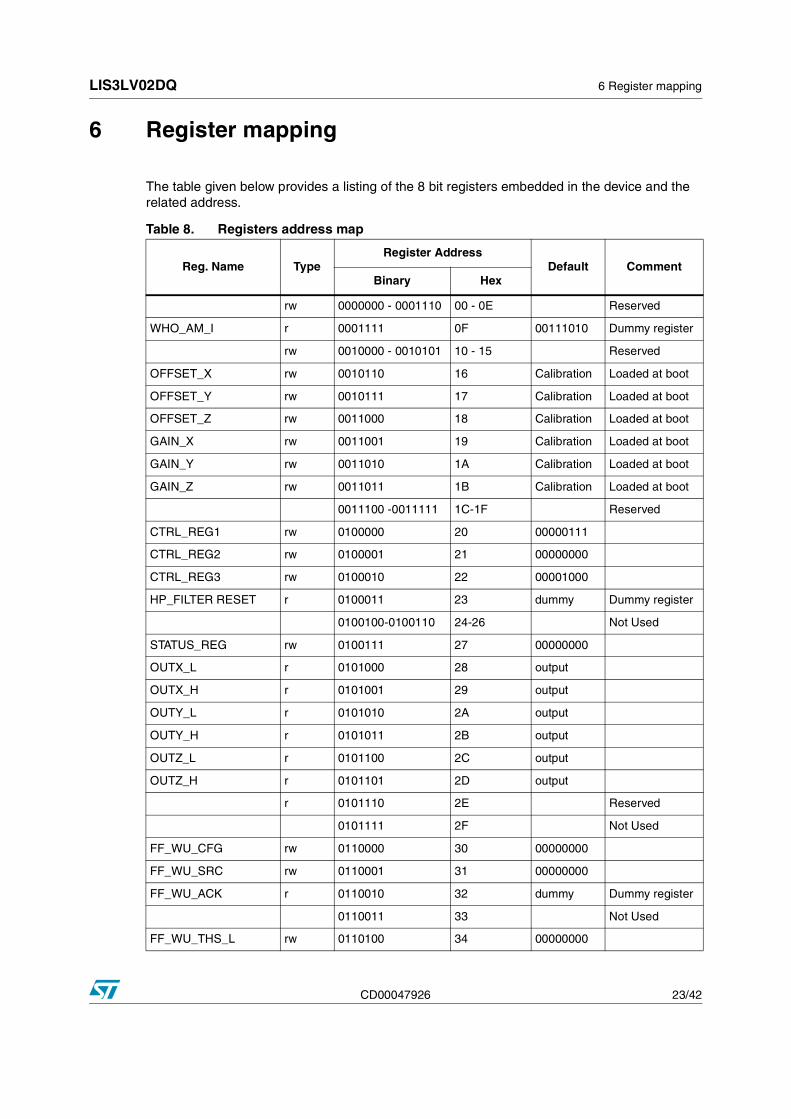
LIS3LV02DQ 6 Register mapping
6 Register mapping
The table given below provides a listing of the 8 bit registers embedded in the device and the related address.
Table 8. Registers address map
Reg. Name TypeRegister Address
Default CommentBinary Hex
rw 0000000 - 0001110 00 - 0E Reserved
WHO_AM_I r 0001111 0F 00111010 Dummy register
rw 0010000 - 0010101 10 - 15 Reserved
OFFSET_X rw 0010110 16 Calibration Loaded at boot
OFFSET_Y rw 0010111 17 Calibration Loaded at boot
OFFSET_Z rw 0011000 18 Calibration Loaded at boot
GAIN_X rw 0011001 19 Calibration Loaded at boot
GAIN_Y rw 0011010 1A Calibration Loaded at boot
GAIN_Z rw 0011011 1B Calibration Loaded at boot
0011100 -0011111 1C-1F Reserved
CTRL_REG1 rw 0100000 20 00000111
CTRL_REG2 rw 0100001 21 00000000
CTRL_REG3 rw 0100010 22 00001000
HP_FILTER RESET r 0100011 23 dummy Dummy register
0100100-0100110 24-26 Not Used
STATUS_REG rw 0100111 27 00000000
OUTX_L r 0101000 28 output
OUTX_H r 0101001 29 output
OUTY_L r 0101010 2A output
OUTY_H r 0101011 2B output
OUTZ_L r 0101100 2C output
OUTZ_H r 0101101 2D output
r 0101110 2E Reserved
0101111 2F Not Used
FF_WU_CFG rw 0110000 30 00000000
FF_WU_SRC rw 0110001 31 00000000
FF_WU_ACK r 0110010 32 dummy Dummy register
0110011 33 Not Used
FF_WU_THS_L rw 0110100 34 00000000
CD00047926 23/42

6 Register mapping LIS3LV02DQ
Registers marked as reserved must not be changed. The writing to those registers may cause permanent damages to the device.
The content of the registers that are loaded at boot should not be changed. They contain the factory calibration values. Their content is automatically restored when the device is powered-up.
FF_WU_THS_H rw 0110101 35 00000000
FF_WU_DURATION rw 0110110 36 00000000
0110111 37 Not Used
DD_CFG rw 0111000 38 00000000
DD_SRC rw 0111001 39 00000000
DD_ACK r 0111010 3A dummy Dummy register
0111011 3B Not Used
DD_THSI_L rw 0111100 3C 00000000
DD_THSI_H rw 0111101 3D 00000000
DD_THSE_L rw 0111110 3E 00000000
DD_THSE_H rw 0111111 3F 00000000
1000000-1111111 40-7F Reserved
Table 8. Registers address map (continued)
Reg. Name TypeRegister Address
Default CommentBinary Hex
24/42 CD00047926

LIS3LV02DQ 7 Register Description
7 Register Description
The device contains a set of registers which are used to control its behavior and to retrieve acceleration data. The registers 7.2 to 7.7 contain the factory calibration values, it is not necessary to change their value for normal device operation.
7.1 WHO_AM_I (0Fh)
Addressing this register the physical address of the device is returned. For LIS3LV02DQ the physical address assigned in factory is 3Ah.
7.2 OFFSET_X (16h)
7.3 OFFSET_Y (17h)
7.4 OFFSET_Z (18h)
W7 W6 W5 W4 W3 W2 W1 W0
W7, W0 LIS3LV02DQ Physical Address equal to 3Ah
OX7 OX6 OX5 OX4 OX3 OX2 OX1 OX0
OX7, OX0 Digital Offset Trimming for X-Axis
OY7 OY6 OY5 OY4 OY3 OY2 OY1 OY0
DOY7, DOY0 Digital Offset Trimming for Y-Axis
OZ7 OZ6 OZ5 OZ4 OZ3 OZ2 OZ1 OZ0
OZ7, OZ0 Digital Offset Trimming for Z-Axis
CD00047926 25/42
7 Register Description LIS3LV02DQ
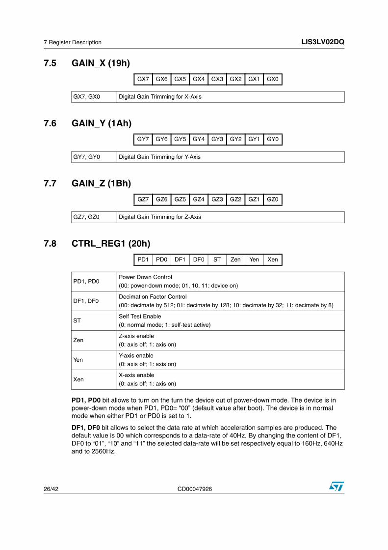
7.5 GAIN_X (19h)
7.6 GAIN_Y (1Ah)
7.7 GAIN_Z (1Bh)
7.8 CTRL_REG1 (20h)
PD1, PD0 bit allows to turn on the turn the device out of power-down mode. The device is in power-down mode when PD1, PD0= “00” (default value after boot). The device is in normal mode when either PD1 or PD0 is set to 1.
DF1, DF0 bit allows to select the data rate at which acceleration samples are produced. The default value is 00 which corresponds to a data-rate of 40Hz. By changing the content of DF1, DF0 to “01”, “10” and “11” the selected data-rate will be set respectively equal to 160Hz, 640Hz and to 2560Hz.
GX7 GX6 GX5 GX4 GX3 GX2 GX1 GX0
GX7, GX0 Digital Gain Trimming for X-Axis
GY7 GY6 GY5 GY4 GY3 GY2 GY1 GY0
GY7, GY0 Digital Gain Trimming for Y-Axis
GZ7 GZ6 GZ5 GZ4 GZ3 GZ2 GZ1 GZ0
GZ7, GZ0 Digital Gain Trimming for Z-Axis
PD1 PD0 DF1 DF0 ST Zen Yen Xen
PD1, PD0Power Down Control
(00: power-down mode; 01, 10, 11: device on)
DF1, DF0Decimation Factor Control
(00: decimate by 512; 01: decimate by 128; 10: decimate by 32; 11: decimate by 8)
STSelf Test Enable
(0: normal mode; 1: self-test active)
ZenZ-axis enable
(0: axis off; 1: axis on)
YenY-axis enable
(0: axis off; 1: axis on)
XenX-axis enable
(0: axis off; 1: axis on)
26/42 CD00047926

LIS3LV02DQ 7 Register Description
ST bit is used to activate the self test function. When the bit is set to one, an output change will occur to the device outputs (refer to table 2 and 3 for specification) thus allowing to check the functionality of the whole measurement chain.
Zen bit enables the Z-axis measurement channel when set to 1. The default value is 1.
Yen bit enables the Y-axis measurement channel when set to 1. The default value is 1.
Xen bit enables the X-axis measurement channel when set to 1. The default value is 1.
7.9 CTRL_REG2 (21h)
FS bit is used to select Full Scale value. After the device power-up the default full scale value is +/-2g. In order to obtain a +/-6g full scale it is necessary to set FS bit to ‘1’.
BDU bit is used to inhibit output registers update until both upper and lower register parts are read. In default mode (BDU= ‘0’) the output register values are updated continuously. If for any reason it is not sure to read faster than output data rate it is recommended to set BDU bit to ‘1’. In this way the content of output registers is not updated until both MSB and LSB are read avoiding to read values related to different sample time.
BLE bit is used to select Big Endian or Little Endian representation for output registers. In Big Endian’s one MSB acceleration value is located at addresses 28h (X-axis), 2Ah (Y-axis) and 2Ch (Z-axis) while LSB acceleration value is located at addresses 29h (X-axis), 2Bh (Y-axis) and 2Dh (Z-axis). In Little Endian representation (Default, BLE=‘0‘) the order is inverted (refer to data register description for more details).
BOOT bit is used to refresh the content of internal registers stored in the flash memory block. At the device power up the content of the flash memory block is transferred to the internal registers related to trimming functions to permit a good behavior of the device itself. If for any reason the content of trimming registers was changed it is sufficient to use this bit to restore correct values. When BOOT bit is set to ‘1’ the content of internal flash is copied inside corresponding internal registers and it is used to calibrate the device. These values are factory
FS BDU BLE BOOT IEN DRDY SIM DAS
FSFull Scale selection
(0: ±2g; 1: ±6g)
BDUBlock Data Update
(0: continuous update; 1: output registers not updated until MSB and LSB reading)
BLEBig/Little Endian selection
(0: little endian; 1: big endian)
BOOT Reboot memory content
IENInterrupt ENable
(0: data ready on RDY pad; 1: int req on RDY pad)
DRDY Enable Data-Ready generation
SIMSPI Serial Interface Mode selection
(0: 4-wire interface; 1: 3-wire interface)
DASData Alignment Selection
(0: 12 bit right justified; 1: 16 bit left justified)
CD00047926 27/42
7 Register Description LIS3LV02DQ
trimmed and they are different for every accelerometer. They permit a good behavior of the device and normally they have not to be changed. At the end of the boot process the BOOT bit is set again to ‘0’.
IEN bit is used to switch the value present on data-ready pad between Data-Ready signal and Interrupt signal. At power up the Data-ready signal is chosen. It is however necessary to modify DRDY bit to enable Data-Ready signal generation.
DRDY bit is used to enable Data-Ready (RDY/INT) pin activation. If DRDY bit is ‘0’ (default value) on Data-Ready pad a ‘0’ value is present. If a Data-Ready signal is desired it is necessary to set to ‘1’ DRDY bit. Data-Ready signal goes to ‘1’ whenever a new data is available for all the enabled axis. For example if Z-axis is disabled, Data-Ready signal goes to ‘1’ when new values are available for both X and Y axis. Data-Ready signal comes back to ‘0’ when all the registers containing values of the enabled axis are read. To be sure not to loose any data coming from the accelerometer data registers must be read before a new Data-Ready rising edge is generated. In this case Data-ready signal will have the same frequency of the data rate chosen.
SIM bit selects the SPI Serial Interface Mode. When SIM is ‘0’ (default value) the 4-wire interface mode is selected. The data coming from the device are sent to SDO pad. In 3-wire interface mode output data are sent to SDA_SDI pad.
DAS bit permits to decide between 12 bit right justified and 16 bit left justified representation of data coming from the device. The first case is the default case and the most significant bits are replaced by the bit representing the sign.
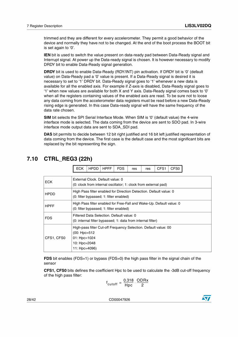
7.10 CTRL_REG3 (22h)
FDS bit enables (FDS=1) or bypass (FDS=0) the high pass filter in the signal chain of the sensor
CFS1, CFS0 bits defines the coefficient Hpc to be used to calculate the -3dB cut-off frequency of the high pass filter:
ECK HPDD HPFF FDS res res CFS1 CFS0
ECKExternal Clock. Default value: 0
(0: clock from internal oscillator; 1: clock from external pad)
HPDDHigh Pass filter enabled for Direction Detection. Default value: 0
(0: filter bypassed; 1: filter enabled)
HPFFHigh Pass filter enabled for Free-Fall and Wake-Up. Default value: 0
(0: filter bypassed; 1: filter enabled)
FDSFiltered Data Selection. Default value: 0
(0: internal filter bypassed; 1: data from internal filter)
CFS1, CFS0
High-pass filter Cut-off Frequency Selection. Default value: 00
(00: Hpc=512
01: Hpc=1024
10: Hpc=2048
11: Hpc=4096)
fcutoff0.318Hpc
--------------- ODRx2
-----------------⋅=
28/42 CD00047926

LIS3LV02DQ 7 Register Description
7.11 HP_FILTER_RESET (23h)
Dummy register. Reading at this address zeroes instantaneously the content of the internal high pass-filter. Read data is not significant.
7.12 STATUS_REG (27h)
7.13 OUTX_L (28h)
In Big Endian Mode (bit BLE CTRL_REG2 set to ‘1’) the content of this register is the MSB acceleration data and depends by bit DAS in CTR_REG2 reg as described in the following section.
7.14 OUTX_H (29h)
When reading the register in “12 bit right justified” mode the most significant bits (15:12) are replaced with bit 11 (i.e. XD15-XD12=XD11, XD11, XD11, XD11).
In Big Endian Mode (bit BLE CTRL_REG2 set to ‘1’) the content of this register is the LSB acceleration data.
ZYXOR ZOR YOR XOR ZYXDA ZDA YDA XDA
ZYXOR X, Y and Z axis Data Overrun
ZOR Z axis Data Overrun
YOR Y axis Data Overrun
XOR X axis Data Overrun
ZYXDA X, Y and Z axis new Data Available
ZDA Z axis new Data Available
YDA Y axis new Data Available
XDA X axis new Data Available
XD7 XD6 XD5 XD4 XD3 XD2 XD1 XD0
XD7, XD0 X axis acceleration data LSB
XD15 XD14 XD13 XD12 XD11 XD10 XD9 XD8
XD15, XD8 X axis acceleration data MSB
CD00047926 29/42
7 Register Description LIS3LV02DQ
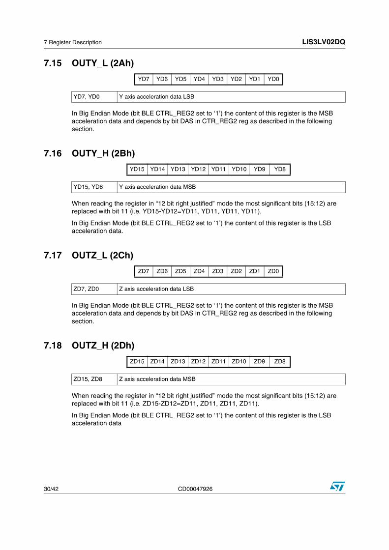
7.15 OUTY_L (2Ah)
In Big Endian Mode (bit BLE CTRL_REG2 set to ‘1’) the content of this register is the MSB acceleration data and depends by bit DAS in CTR_REG2 reg as described in the following section.
7.16 OUTY_H (2Bh)
When reading the register in “12 bit right justified” mode the most significant bits (15:12) are replaced with bit 11 (i.e. YD15-YD12=YD11, YD11, YD11, YD11).
In Big Endian Mode (bit BLE CTRL_REG2 set to ‘1’) the content of this register is the LSB acceleration data.
7.17 OUTZ_L (2Ch)
In Big Endian Mode (bit BLE CTRL_REG2 set to ‘1’) the content of this register is the MSB acceleration data and depends by bit DAS in CTR_REG2 reg as described in the following section.
7.18 OUTZ_H (2Dh)
When reading the register in “12 bit right justified” mode the most significant bits (15:12) are replaced with bit 11 (i.e. ZD15-ZD12=ZD11, ZD11, ZD11, ZD11).
In Big Endian Mode (bit BLE CTRL_REG2 set to ‘1’) the content of this register is the LSB acceleration data
YD7 YD6 YD5 YD4 YD3 YD2 YD1 YD0
YD7, YD0 Y axis acceleration data LSB
YD15 YD14 YD13 YD12 YD11 YD10 YD9 YD8
YD15, YD8 Y axis acceleration data MSB
ZD7 ZD6 ZD5 ZD4 ZD3 ZD2 ZD1 ZD0
ZD7, ZD0 Z axis acceleration data LSB
ZD15 ZD14 ZD13 ZD12 ZD11 ZD10 ZD9 ZD8
ZD15, ZD8 Z axis acceleration data MSB
30/42 CD00047926

LIS3LV02DQ 7 Register Description
7.19 FF_WU_CFG (30h)
Free-fall and inertial wake-up configuration register.
AOI LIR ZHIE ZLIE YHIE YLIE XHIE XLIE
AOI
And/Or combination of Interrupt events interrupt request. Default value: 0.
(0: OR combination of interrupt events;
1: AND combination of interrupt events)
LIR
Latch interrupt request. Default value: 0.
(0: interrupt request not latched;
1: interrupt request latched)
ZHIE
Enable Interrupt request on Z high event. Default value: 0.
(0: disable interrupt request;
1: enable interrupt request on measured accel. value higher than preset threshold)
ZLIE
Enable Interrupt request on Z low event. Default value: 0.
(0: disable interrupt request;
1: enable interrupt request on measured accel. value lower than preset threshold)
YHIE
Enable Interrupt request on Y high event. Default value: 0.
(0: disable interrupt request;
1: enable interrupt request on measured accel. value higher than preset threshold)
YLIE
Enable Interrupt request on Y low event. Default value: 0.
(0: disable interrupt request;
1: enable interrupt request on measured accel. value lower than preset threshold)
XHIE
Enable Interrupt request on X high event. Default value: 0.
(0: disable interrupt request;
1: enable interrupt request on measured accel. value higher than preset threshold)
XLIE
Enable Interrupt request on X low event. Default value: 0.
(0: disable interrupt request;
1: enable interrupt request on measured accel. value lower than preset threshold)
CD00047926 31/42

7 Register Description LIS3LV02DQ
7.20 FF_WU_SRC (31h)
7.21 FF_WU_ACK (32h)
Dummy register. If LIR bit in FF_WU_CFG=1 allows the refresh of FF_WU_SRC. Read data is not significant.
X IA ZH ZL YH YL XH XL
IA
Interrupt Active. Default value: 0
(0: no interrupt has been generated;
1: one or more interrupt event has been generated)
ZHZ High. Default value: 0
(0: no interrupt; 1: ZH event has occurred)
ZLZ Low. Default value: 0
(0: no interrupt; 1: ZL event has occurred)
YHY High. Default value: 0
(0: no interrupt; 1: YH event has occurred)
YLY Low. Default value: 0
(0: no interrupt; 1: YL event has occurred)
XHX High. Default value: 0
(0: no interrupt; 1: XH event has occurred)
XLX Low. Default value: 0
(0: no interrupt; 1: XL event has occurred)
32/42 CD00047926

LIS3LV02DQ 7 Register Description
7.22 FF_WU_THS_L (34h)
7.23 FF_WU_THS_H (35h)
7.24 FF_WU_DURATION (36h)
Set the minimum duration of the free-fall/wake-up event to be recognized.
THS7 THS6 THS5 THS4 THS3 THS2 THS1 THS0
THS7, THS0 Free-fall / Inertial Wake Up Acceleration Threshold LSB
THS15 THS14 THS13 THS12 THS11 THS10 THS9 THS8
THS15, THS8 Free-fall / Inertial Wake Up Acceleration Threshold MSB
FWD7 FWD6 FWD5 FWD4 FWD3 FWD2 FWD1 FWD0
FWD7, FWD0 Minimum duration of the Free-fall/Wake-up event
Duration s( ) FF_WU_Duration (Dec)ODR
---------------------------------------------------------------=
CD00047926 33/42

7 Register Description LIS3LV02DQ
7.25 DD_CFG (38h)
Direction-detector configuration register
IEND LIR ZHIE ZLIE YHIE YLIE XHIE XLIE
IEND
Interrupt enable on Direction change. Default value: 0
(0: disabled;
1: interrupt signal enabled)
LIR
Latch Interrupt request into DD_SRC reg with the DD_SRC reg cleared by reading
DD_ACK reg. Default value: 0.
(0: interrupt request not latched;
1: interrupt request latched)
ZHIE
Enable interrupt generation on Z high event. Default value: 0
(0: disable interrupt request;
1: enable interrupt request on measured accel. value higher than preset threshold)
ZLIE
Enable interrupt generation on Z low event. Default value: 0
(0: disable interrupt request;
1: enable interrupt request on measured accel. value lower than preset threshold)
YHIE
Enable interrupt generation on Y high event. Default value: 0
(0: disable interrupt request;
1: enable interrupt request on measured accel. value higher than preset threshold)
YLIE
Enable interrupt generation on Y low event. Default value: 0
(0: disable interrupt request;
1: enable interrupt request on measured accel. value lower than preset threshold)
XHIE
Enable interrupt generation on X high event. Default value: 0
(0: disable interrupt request;
1: enable interrupt request on measured accel. value higher than preset threshold)
XLIE
Enable interrupt generation on X low event. Default value: 0
(0: disable interrupt request;
1: enable interrupt request on measured accel. value lower than preset threshold)
34/42 CD00047926

LIS3LV02DQ 7 Register Description
7.26 DD_SRC (39h)
Direction detector source register
7.27 DD_ACK (3Ah)
Dummy register. If LIR bit in DD_CFG=1 allows the refresh of DD_SRC. Read data is not significant.
X IA ZH ZL YH YL XH XL
IA
Interrupt event from direction change.
(0: no direction changes detected;
1: direction has changed from previous measurement)
ZH
Z High. Default value: 0
(0: Z below THSI threshold;
1: Z accel. exceeding THSE threshold along positive direction of acceleration axis)
ZL
Z Low. Default value: 0
(0: Z below THSI threshold;
1: Z accel. exceeding THSE threshold along negative direction of acceleration axis)
YH
Y High. Default value: 0
(0: Y below THSI threshold;
1: Y accel. exceeding THSE threshold along positive direction of acceleration axis)
YL
Y Low. Default value: 0
(0: Y below THSI threshold;
1: Y accel. exceeding THSE threshold along negative direction of acceleration axis)
XH
X High. Default value: 0
(0: X below THSI threshold;
1: X accel. exceeding THSE threshold along positive direction of acceleration axis)
XL
X Low. Default value: 0
(0: X below THSI threshold;
1: X accel. exceeding THSE threshold along negative direction of acceleration axis)
CD00047926 35/42

7 Register Description LIS3LV02DQ
7.28 DD_THSI_L (3Ch)
7.29 DD_THSI_H (3Dh)
7.30 DD_THSE_L (3Eh)
7.31 DD_THSE_H (3Fh)
THSI7 THSI6 THSI5 THSI4 THSI3 THSI2 THSI1 THSI0
THSI7, THSI0 Direction detection Internal Threshold LSB
THSI15 THSI14 THSI13 THSI12 THSI11 THSI10 THSI9 THSI8
THSI15, THSI8 Direction detection Internal Threshold MSB
THSE7 THSE6 THSE5 THSE4 THSE3 THSE2 THSE1 THSE0
THSE7, THSE0 Direction detection External Threshold LSB
THSE15 THSE14 THSE13 THSE12 THSE11 THSE10 THSE9 THSE8
THSE15, THSE8 Direction detection External Threshold MSB
36/42 CD00047926

LIS3LV02DQ 8 Typical performance characteristics
8 Typical performance characteristics
8.1 Mechanical Characteristics at 25°C
Figure 10. x-axis 0-g level at 2.5V Figure 11. y-axis 0-g level at 2.5V
Figure 12. z-axis 0-g level at 2.5V Figure 13. x-axis sensitivity at 2.5V
Figure 14. y-axis sensitivity at 2.5V Figure 15. z-axis sensitivity at 2.5V
−10 −5 0 5 100
2
4
6
8
10
12
14
16
18
20
0−g LEVEL (mg)
Per
cent
of p
arts
(%
)
−10 −5 0 5 100
5
10
15
20
25
0−g LEVEL (mg)P
erce
nt o
f par
ts (
%)
−20 −15 −10 −5 0 5 10 15 200
5
10
15
20
25
0−g LEVEL (mg)
Per
cent
of p
arts
(%
)
1010 1015 1020 1025 10300
2
4
6
8
10
12
14
16
18
20
sensitivity (LSb/g)
Per
cent
of p
arts
(%
)
1010 1015 1020 1025 10300
2
4
6
8
10
12
14
16
18
20
sensitivity (LSb/g)
Per
cent
of p
arts
(%
)
1010 1015 1020 1025 10300
2
4
6
8
10
12
14
16
18
20
sensitivity (LSb/g)
Per
cent
of p
arts
(%
)
CD00047926 37/42
8 Typical performance characteristics LIS3LV02DQ
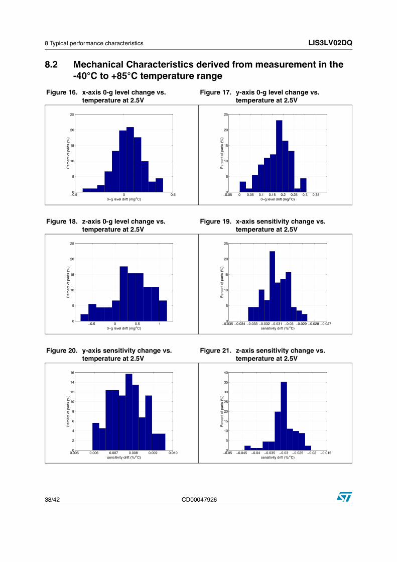
8.2 Mechanical Characteristics derived from measurement in the-40°C to +85°C temperature range
Figure 16. x-axis 0-g level change vs. temperature at 2.5V
Figure 17. y-axis 0-g level change vs. temperature at 2.5V
Figure 18. z-axis 0-g level change vs. temperature at 2.5V
Figure 19. x-axis sensitivity change vs. temperature at 2.5V
Figure 20. y-axis sensitivity change vs. temperature at 2.5V
Figure 21. z-axis sensitivity change vs. temperature at 2.5V
−0.5 0 0.50
5
10
15
20
25
0−g level drift (mg/οC)
Per
cent
of p
arts
(%
)
−0.05 0 0.05 0.1 0.15 0.2 0.25 0.3 0.350
5
10
15
20
25
0−g level drift (mg/οC)
Per
cent
of p
arts
(%
)
−0.5 0 0.5 10
5
10
15
20
25
0−g level drift (mg/οC)
Per
cent
of p
arts
(%
)
−0.035 −0.034 −0.033 −0.032 −0.031 −0.03 −0.029 −0.028 −0.0270
5
10
15
20
25
sensitivity drift (%/οC)
Per
cent
of p
arts
(%
)
0.005 0.006 0.007 0.008 0.009 0.0100
2
4
6
8
10
12
14
16
sensitivity drift (%/οC)
Per
cent
of p
arts
(%
)
−0.05 −0.045 −0.04 −0.035 −0.03 −0.025 −0.02 −0.0150
5
10
15
20
25
30
35
40
sensitivity drift (%/οC)
Per
cent
of p
arts
(%
)
38/42 CD00047926

LIS3LV02DQ 8 Typical performance characteristics
8.3 Electro-Mechanical characteristics at 25°C
Figure 22. x and y axis 0-g level as function of supply voltage
Figure 23. z axis 0-g level as function of supply voltage
Figure 24. Current consumption in Power-Down mode (Vdd=2.5V)
Figure 25. Current consumption in Operational mode (Vdd=2.5V)
2 2.2 2.4 2.6 2.8 3 3.2 3.4 3.6−80
−60
−40
−20
0
20
40
60
80
0−g
leve
l (m
g)
Supply Voltage (V)2 2.2 2.4 2.6 2.8 3 3.2 3.4 3.6
−80
−60
−40
−20
0
20
40
60
80
0−g
leve
l (m
g)
Supply Voltage (V)
−5 0 50
5
10
15
20
25
30
current consumption (uA)
Per
cent
of p
arts
(%
)
500 550 600 650 7000
2
4
6
8
10
12
14
16
18
20
current consumption (uA)
Per
cent
of p
arts
(%
)
CD00047926 39/42

9 Package Information LIS3LV02DQ
9 Package Information
In order to meet environmental requirements, ST offers these devices in ECOPACK® packages. These packages have a Lead-free second level interconnect. The category of second Level Interconnect is marked on the package and on the inner box label, in compliance with JEDEC Standard JESD97. The maximum ratings related to soldering conditions are also marked on the inner box label. ECOPACK is an ST trademark.
ECOPACK specifications are available at: www.st.com.
Figure 26. QFPN-28 Mechanical Data & Package Dimensions
OUTLINE ANDMECHANICAL DATA
DIM.mm inch
MIN. TYP. MAX. MIN. TYP. MAX.
A 1.70 1.80 1.90 0.067 0.071 0.075
A1 0.05 0.002
A3 0.203 0.008
b 0.30 0.35 0.40 0.012 0.014 0.016
D 6.85 7.0 7.15 0.270 0.275 0.281
D1 4.90 5.00 5.10 0.192 0.197 0.20
E 6.85 7.0 7.15 0.270 0.275 0.281
E1 4.90 5.00 5.10 0.192 0.197 0.20
e 0.80 0.0315
L 0.45 0.55 0.65 0.018 0..022 0.025
L1 0.10 0.004
ddd 0.08 0.003
QFPN-28 (7x7x1.8mm)Quad Flat Package No lead
7787120 C
40/42 CD00047926

LIS3LV02DQ 10 Revision history
10 Revision history
Date Revision Changes
7-Oct-2005 1 Initial release.
CD00047926 41/42

LIS3LV02DQ
Information furnished is believed to be accurate and reliable. However, STMicroelectronics assumes no responsibility for the consequencesof use of such information nor for any infringement of patents or other rights of third parties which may result from its use. No license is grantedby implication or otherwise under any patent or patent rights of STMicroelectronics. Specifications mentioned in this publication are subjectto change without notice. This publication supersedes and replaces all information previously supplied. STMicroelectronics products are notauthorized for use as critical components in life support devices or systems without express written approval of STMicroelectronics.
The ST logo is a registered trademark of STMicroelectronics.All other names are the property of their respective owners
© 2005 STMicroelectronics - All rights reserved
STMicroelectronics group of companies
Australia - Belgium - Brazil - Canada - China - Czech Republic - Finland - France - Germany - Hong Kong - India - Israel - Italy - Japan - Malaysia - Malta - Morocco - Singapore - Spain - Sweden - Switzerland - United Kingdom - United States of America
www.st.com
42/42 CD00047926