MEMS BASED RESONANT MASS SENSORS WITH …etd.lib.metu.edu.tr/upload/12619097/index.pdf · Anahtar...
116
MEMS BASED RESONANT MASS SENSORS WITH FEEDTHROUGH CURRENT ELIMINATION FOR IN-LIQUID CELL DETECTION APPLICATIONS A THESIS SUBMITTED TO THE GRADUATE SCHOOL OF NATURAL AND APPLIED SCIENCES OF MIDDLE EAST TECHNICAL UNIVERSITY BY MUSTAFA KANGÜL IN PARTIAL FULFILLMENT OF THE REQUIREMENTS FOR THE DEGREE OF MASTER OF SCIENCE IN ELECTRICAL AND ELECTRONICS ENGINEERING SEPTEMBER 2015
Transcript of MEMS BASED RESONANT MASS SENSORS WITH …etd.lib.metu.edu.tr/upload/12619097/index.pdf · Anahtar...

MEMS BASED RESONANT MASS SENSORS WITH FEEDTHROUGH
CURRENT ELIMINATION FOR IN-LIQUID CELL DETECTION
APPLICATIONS
A THESIS SUBMITTED TO
THE GRADUATE SCHOOL OF NATURAL AND APPLIED SCIENCES
OF
MIDDLE EAST TECHNICAL UNIVERSITY
BY
MUSTAFA KANGÜL
IN PARTIAL FULFILLMENT OF THE REQUIREMENTS
FOR
THE DEGREE OF MASTER OF SCIENCE
IN
ELECTRICAL AND ELECTRONICS ENGINEERING
SEPTEMBER 2015


Approval of the thesis:
MEMS BASED RESONANT MASS SENSORS WITH FEEDTHROUGH
CURRENT ELIMINATION FOR IN-LIQUID CELL DETECTION
APPLICATIONS
submitted by MUSTAFA KANGÜL in partial fulfillment of the requirements for
the degree of Master of Science in Electrical and Electronics Engineering
Department, Middle East Technical University by,
Prof. Dr. Gülbin Dural Ünver
Dean, Graduate School of Natural and Applied Sciences
Prof. Dr. Gönül Turhan Sayan
Head of Department, Electrical and Electronics Engineering
Prof. Dr. Haluk Külah
Supervisor, Electrical and Electronics Eng. Dept., METU
Examining Committee Members:
Prof. Dr. Tayfun Akın
Electrical and Electronics Engineering Dept., METU
Prof. Dr. Haluk Külah
Electrical and Electronics Engineering Dept., METU
Assoc. Prof. Yeşim Serinağaoğlu Doğrusöz
Electrical and Electronics Engineering Dept., METU
Asst. Prof. Dr. Kıvanç Azgın
Electrical and Electronics Engineering Dept., METU
Asst. Prof. Dr. M. Yusuf Tanrıkulu
Electrical and Electronics Engineering Dept., Adana STU
Date:

iv
I hereby declare that all information in this document has been obtained and
presented in accordance with academic rules and ethical conduct. I also
declare that, as required by these rules and conduct, I have fully cited and
referenced all material and results that are not original to this work.
Name, Lastname: Mustafa Kangül
Signature:

v
ABSTRACT
DEVELOPMENT OF
RESONANT MASS SENSORS FOR MEMS
BASED
REAL TIME CELL DETECTION APPLICATIONS
Kangül, Mustafa
M. S., Department of Electrical and Electronics Engineering
Supervisor: Prof. Dr. Haluk Külah
September 2015, 98 pages
This thesis represents design and implementation of MEMS based resonant mass
sensors for cell detection applications. The main objective of the thesis is real-time
detection inside liquid medium and obtaining the results by electronic means,
without the assistance of bulky optical instruments.
Novel resonant based mass sensor architectures that have various improvements
over selected benchmark design are presented. Purpose of the new structures is to
establish real-time mass detection by improving the quality factor, increasing the
sensor gain and eliminating the feedthrough current effect. Proposed sensors
oscillate in the lateral direction and are coated with a thin parylene layer to prevent
liquids flow through the narrow gaps of the device, further improving the quality
factor. The resonator is located on top of a microchannel. A thin gold film on the
oscillating proof mass is employed as an antibody based cell capture surface.
Theoretical background of the physical resonators is investigated to diagnose the
design issues of the sensors in the literature. Capacitive actuation, sensing
optimization, and feedthrough current elimination methods are presented. In the
vi
light of these theoretical studies and finite element modeling simulations, four new
resonating structures are proposed for the purpose of real-time mass sensing by
enabling self-oscillation.
A new process flow consisting SOI, glass, and polymer micromachining methods
has been utilized for resonator fabrication. Each device has a foot print area of 18 x
6 mm2, a significant percent of which is used for the inlet and outlet connections of
the microchannels.
Resonance characterization results in air are presented to see the improvements over
the benchmark design, which is previously developed in METU BioMEMS research
group. Total sensor mass has been decreased without any loss in the sensor gain.
Even two orders of magnitude increase in the gain is achieved with the same mass.
There is also quality factor enhancement up to ten times. These improvements are
established without changing the anchor structure or cell capturing surface area of
the benchmark design. Feedthrough current is also eliminated to make self-
oscillation possible. According to the conducted mass measurement results, the mass
of a single Sigma-Aldrich® polystyrene microbead is 0.53 ng, whereas the mass is
given as 0.55 ng ±30% in its datasheet. In-liquid functionality was also tested. The
quality factor of the sensor is reduced from 402, in air, to only to 183 in wet
environment. Reported improvements enable real time cell detection in liquid
environment.
Keywords: Resonant mass sensor, cell detection, parylene, hydrophobic coating,
quality factor improvement, microresonator, fabrication of suspended structures.
vii
ÖZ
SIVI ORTAMDA HÜCRE TESPİTİ UYGULAMALARI
İÇİN KAÇAK AKIMI ELEYEN MEMS TABANLI
RESONANT KÜTLE SENSÖRLERİ
Kangül, Mustafa
Yüksek Lisans, Elektrik ve Elektronik Mühendisliği Bölümü
Tez Yöneticisi: Prof. Dr. Haluk Külah
Eylül 2015, 98 sayfa
Bu tez gerçek zamanli hücre tespiti uygulamalari için MEMS tabanli ataletsel
rezonatör sensörleri geliştirilmesini anlatmaktadır. Tezin temel amacı optik cihazlar
kullanmadan, eletronik arayüz sayesinde sıvı ortamda gerçek zamanlı tespit
yapabilmektir.
Kıyaslanabilecek tasarımlara göre bir çok iyileştirmesi olan özgün resonatör temelli
kütle sensor yapıları sunulmuştur. Yeni yapıların amacı sensör kazancını ve kalite
faktörünü arttırıp elektrik akımını da eleyip gerçek zamanlı tespiti mümkün
kılmaktır. Önerilen sensörler yatay düzlemde salınırlar ve boşluklara sıvı dolmasını
engelleyen ince bir parilen katman ile kaplanmışlardır. Rezonatörler mikrokanalın
üzerine yerletirilmiştir. Salınım yapan kütlenin üzerindeki ince bir altın film
antibody kullanarak hücre yakalamayı mümkün kılmaktadır.
Fiziksel rezönatör yapılarının teorik altyapısı araştırılmıştır. Bu sayede literatürdeki
sensörlerin eksikliklerinin tanısı konulmuştur. Kapasitif harekete geçirme ve
algılama optimizasyonları yapılmış, istenmeyen çıkış akımlarını elemek için
metodlar önerilmiştir. Bu bilgiler ışığında dört yeni rezönatör yapısı tasarlanmıştır.

viii
SOI, cam ve polimer üretim teknikleri kullanılarak oluşturulan üretim şeması
verilmiştir. Üretilen her cihaz 18 x 6 mm2 lik alan kaplamaktadır.
Sensörlerin havadaki rezonans karakteristikleri çıkarılmış, literature göre kaydedilen
ilerlemeler tespit edilmiştir. Sensör kazancının büyüklüğü sensör kütlesi
değiştirilmeden 100 kata kadar arttırılmıştır. Kalite faktörü de 10 katına kadar
çıkarılmıştır. Bu iyileştirmeler hücre yakalamak için ayrılmış alanda ya da asılı
duran sensörü tutan yapılarda herhangi bir değişiklik yapılmadan elde edilmiştir.
Kütle ölçümü deneyi mikro parçacıklarla yapılmış ve bir tanesinin ağırlığı 0.53 ng
olarak ölçülmüştür. Sıvı ortamdaki performansı da test edilmiş olup havada 402
olarak ölçülen kalite faktörünün sadece 183’e düştüğü gözlenmiştir. Raporlanan bu
gelişmeler için gerçek zamanlı hücre tespiti mümkün kılınmıştır.
Anahtar Kelimeler: Ataletsel rezönatör, hücre algılama, parylene hidrofobik
kaplama, kalite faktörü iyileştirilmesi, havada asılı yapıların üretilmesi.

ix
To my family

x
ACKNOWLEDGEMENTS
I would like to express my deep thanks to my thesis advisor, Prof. Dr. Haluk Külah,
for the support and guidance he gave me during my graduate study and also for
giving me the opportunity to work on an exciting project. I would also like to thank
Prof. Dr. Tayfun Akın for his contributions and supports during my studies.
I would like to thank Taylan Töral for developing the previous fabrication process
flow and accompanying me in the long cleanroom hours. I am also thankful to my
new project partners Eren Aydın and Furkan Gökçe for their immense contributions
to the project and this thesis study, both in the design and testing phases. I would
like to express my gratitude to Dr. Ebrü Özgür and Dr. Özge Zorlu for their patience
and helps during my thesis especially in writing phases. I am especially thankful to
all my lab friends in the BioMEMS and PowerMEMS groups: Hasan Uluşan
Yağmur Demircan Yalçın, Özgen Sümer Laçın, Gürhan Özkayar, Hatice Ceylan,
Levent Beker, Garsha Bahrieh, Salar Chamanian, Kaveh Gharebaghi, and Aziz
Koyuncuoğlu for being good friends and creating a fun work environment.
My special thanks go to METU-MEMS Center staff for their kind helps in the
cleanroom. Many thanks particularly to Orhan Akar for sharing his deep knowledge
on microfabrication and for his helps in the cleanroom.
I am grateful to İlker Karakaşoğlu, Nazlı Demirer and Şeyma Edikli for their endless
supports. Ali Günay, Atilla Eyüpoğlu, Ayşegül Çelik, Hatice İçer, Mert Gençtürk,
Özgen Muzaç and Sinan Dirlik also deserve thanks for their priceless friendships.
My special thanks go to Melek Türkmen, the ultimate rahle, for being the joy of my
life.
Finally, I would like to express my deepest gratitude to my parents Sabri and Birgül
Kangül and my sister Dilan for their never-ending support, encouragement and
unconditional love through all my life.

xi
TABLE OF CONTENTS
ABSTRACT ................................................................................................................ v
ÖZ ..............................................................................................................................vii
ACKNOWLEDGEMENTS ....................................................................................... x
TABLE OF CONTENTS .......................................................................................... xi
LIST OF TABLES .................................................................................................. xiii
LIST OF FIGURES ................................................................................................. xiv
CHAPTERS ................................................................................................................ 1
1 INTRODUCTION .............................................................................................. 1
1.1 MICRO SCALE DETECTION TECHNIQUES ..................................................................... 4
1.2 RESONANT BASED GRAVIMETRIC DETECTION ............................................................. 5
1.3 RESEARCH OBJECTIVES AND THESIS ORGANIZATION ................................................... 12
2 THEORY & DESIGN ...................................................................................... 15
2.1 WORKING PRINCIPLES OF A RESONANT BASED CAPACITIVE GRAVIMETRIC SENSOR .......... 15
2.1.1 Resonator Theory................................................................................... 16
2.1.2 Electrostatic Capacitive Actuation and Sensing .................................... 18
2.1.3 The feedthrough current and elimination methods .............................. 25
2.2 DEVICE STRUCTURES AND DESIGN STRATEGIES ......................................................... 32
2.2.1 RCGS#1................................................................................................... 33
2.2.2 RCGS#2................................................................................................... 38
2.2.3 RCGS#3................................................................................................... 42
2.2.4 RCGS#4................................................................................................... 46
2.2.5 RCGS#5................................................................................................... 48
2.2.6 Design Procedure Summary .................................................................. 50
3 FABRICATION ................................................................................................ 53

xii
3.1 PREVIOUS GENERATION PROCESS FLOW ................................................................. 53
3.1.1 Problems related with previous fabrication process flow ..................... 59
3.2 NEW GENERATION PROCESS FLOW ........................................................................ 61
3.3 FABRICATION SUMMARY...................................................................................... 66
4 EXPERIMENTAL RESULTS ........................................................................ 69
4.1 INTERFACE ELECTRONICS ...................................................................................... 69
4.2 EXPERIMENTAL SETUP ......................................................................................... 74
4.3 RESONATOR CHARACTERIZATION ........................................................................... 75
4.3.1 RGCS#1 .................................................................................................. 75
4.3.2 RGCS#2 .................................................................................................. 77
4.3.3 RGCS#3 .................................................................................................. 79
4.3.4 RGCS#4 .................................................................................................. 81
4.3.5 RGCS#5 .................................................................................................. 83
4.4 RESULTS OF FEEDTHROUGH ELIMINATION WITH DUMMY SIGNAL .................................. 87
4.5 MASS SENSING .................................................................................................. 88
4.6 IN-LIQUID RESONANT CHARACTERIZATION ............................................................... 89
5 CONCLUSIONS AND FUTURE WORK ..................................................... 91
REFERENCES ......................................................................................................... 95

xiii
LIST OF TABLES
TABLES
Table 2-1 Important parameters of different resonator designs. ............................... 51
Table 4-1 Important measured parameters of different resonator designs. ............... 86

xiv
LIST OF FIGURES
FIGURES
Figure 1-1 Dimensions of microsystems and biological agents [1] ............................ 2
Figure 1-2 An LoC diagram indicating typical components ...................................... 3
Figure 1-3 Relation of resonance frequency change with system mass change [1]. .. 6
Figure 1-4 Optical (a) and scanning electron micro photographs (b) of the proposed
sensor is presented. Frequency shift at an actuation voltage of 9 V (c) and at
different actuation voltages (d) is also shown [18]. .................................................... 7
Figure 1-5 Illustration of mass measurement by a fluid-filled microcantilever ......... 8
Figure 1-6 Schematic diagram of living cantilever array. As the captured cells are
cultured on the array, their mass changes are measured using the resonance
frequency shift [21]. .................................................................................................... 9
Figure 1-7 Design illustration (a), microscope image of under test device (b) and test
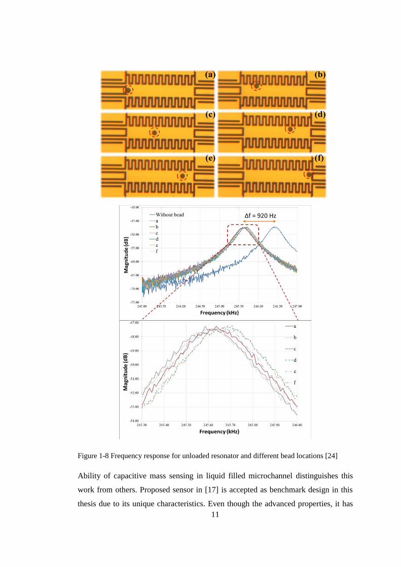
results (c) were presented [16]. ................................................................................. 10
Figure 1-8 Frequency response for unloaded resonator and different bead locations
[24] ............................................................................................................................ 11
Figure 2-1 Schematic view of the second order mass, spring, damper system. ....... 16
Figure 2-2 Schematic view of a parallel plate capacitor with associated variables. . 19
Figure 2-3 A possible frequency response of Equation (2.19) ................................. 22
Figure 2-4 Illustration of varying overlap capacitance ............................................. 23
Figure 2-5 Illustration of varying gap capacitance ................................................... 25
Figure 2-6 Green line denotes the AC response of the resonator only, whereas blue
and red lines show the contribution of feedthrough current on 0.1 fF and 1 fF of
capacitance, respectively. .......................................................................................... 27
Figure 2-7 Two out of phased feedthrough currents cancel each other on sense port.
................................................................................................................................... 28

xv
Figure 2-8. Largest effect of the magnitude mismatch is at Ɵ=180° and amount of
remaining current percentage is equal to the deviation percentage. Whereas effect of
phase deviation is maximum at fully matched gain case and remaining current
percentage is approximately three times of deviation percentage of Ɵ from 180° ... 30
Figure 2-9 Taking difference of the two output currents cancels the same phased
feedthrough current out and adds up oppositely phased resonator related currents. . 31
Figure 2-10 Layout of RCGS#1 ................................................................................ 34
Figure 2-11 Fundamental vibration mode of RCGS#1 is at 230 kHz ....................... 34
Figure 2-12 𝜕𝐶𝜕𝑥𝑠𝑒𝑛𝑠𝑒𝜕𝐶𝜕𝑥𝑎𝑐𝑡.vs displacement for RCGS#1 is drawn where the
red line shows the total result, the dashed black line is the contribution of only
varying gap related term and the solid black line is the contribution of only varying
overlap related term. .................................................................................................. 37
Figure 2-13 𝜕𝐶𝜕𝑥𝑠𝑒𝑛𝑠𝑒𝜕𝐶𝜕𝑥𝑎𝑐𝑡.vs displacement of RCGS#1 for different gaps at
finger ends ................................................................................................................. 38
Figure 2-14 Resonator without finger ....................................................................... 39
Figure 2-15 Fundamental vibration mode of RCGS 1 is at 290 kHz ........................ 39
Figure 2-16 𝜕𝐶𝜕𝑥𝑠𝑒𝑛𝑠𝑒𝜕𝐶𝜕𝑥𝑎𝑐𝑡.vs displacement is drawn for RCGS#1 (the red
line) and RCGS#2 (the blue line). ............................................................................. 41
Figure 2-17 Overall transfer function for resonator with no finger (the red line) and
resonator with comb finger (the blue line) ................................................................ 42
Figure 2-18 Resonator with tree structured finger .................................................... 43
Figure 2-19 Fundamental vibration mode of RCGS 1 is at 239 kHz ........................ 44
Figure 2-20 for 𝜕𝐶𝜕𝑥𝑠𝑒𝑛𝑠𝑒𝜕𝐶𝜕𝑥𝑎𝑐𝑡.vs displacement graph for comb finger and tree
structured finger. ........................................................................................................ 45
Figure 2-21 Resonator with side fingers ................................................................... 46
Figure 2-22 Fundamental vibration mode of RCGS 1 is at 257.9 kHz ..................... 47
Figure 2-23 Diamond shaped resonator .................................................................... 48
Figure 2-24 Fundamental vibration mode of RCGS 1 is at 207.3 kHz ..................... 49
Figure 3-1 Previous generation process flow ............................................................ 54
Figure 3-2 Microscope image of the resonator site of the SOI wafer ....................... 56
Figure 3-3 Microscope image of Glass wafer ........................................................... 57
Figure 3-4 Microscope view through glass wafer after anodic bonding ................... 58

xvi
Figure 3-5 Photograph of a microresonator device fabricated with previous
generation process flow [33]. .................................................................................... 59
Figure 3-6 Gold lines in recess gap creates undesired resistive path between Si
islands. Yellow rectangles show the parts that would be broken by laser cutter in
order to prevent proof mass current leakage. ............................................................ 60
Figure 3-7 Illustration of feedthrough capacitor on resonator .................................. 61
Figure 3-8 New generation fabrication flow ............................................................. 62
Figure 3-9 Microscope image of SOI wafer ............................................................. 63
Figure 3-10 SEM images of each resonator type ...................................................... 64
Figure 3-11 Scanning electron microscope (SEM) view of a resonator after
structural DRIE step .................................................................................................. 65
Figure 3-12 Microscope image of glass wafer after process completed ................... 66
Figure 3-13 Photograph of resonant mass sensor device integrated with microfluidic
channel cap and fluidic connections. ........................................................................ 67
Figure 4-1 Transimpedance amplifier architecture ................................................... 70
Figure 4-2 Phase shifter topology ............................................................................. 71
Figure 4-3 Electronics that presents two out-of-phased output by utilizing
instrumentation amplifiers ........................................................................................ 72
Figure 4-4 Voltage subtractor electronic that is used to eliminate the feedthrough
current ....................................................................................................................... 73
Figure 4-5 A closer look of designed electronics with device under test ................. 73
Figure 4-6 Image of the test setup............................................................................. 74
Figure 4-7 Illustration of the experimental setup for open (black line) and close loop
(blue line) operation of devices................................................................................. 75
Figure 4-8 Magnitude and phase response of system with RGCS#1 (Screen of the
network analyzer)...................................................................................................... 76
Figure 4-9 Magnitude and phase response of RGCS#1 (post-processed data) ......... 77
Figure 4-10 Magnitude and phase response of system with RGCS#2 (Screen of the
network analyzer)...................................................................................................... 78
Figure 4-11 Magnitude and phase response of RGCS#2 (post-processed data) ....... 79
Figure 4-12 Magnitude and phase response of system with RGCS#3 (Screen of the
network analyzer)...................................................................................................... 80

xvii
Figure 4-13 Magnitude and phase response of RGCS#3 (post-processed data) ....... 81
Figure 4-14 Magnitude and phase response of system with RGCS#4 (Screen of the
network analyzer) ...................................................................................................... 82
Figure 4-15 Magnitude and phase response of RGCS#4 (post-processed data) ....... 83
Figure 4-16 Magnitude and phase response of system with RGCS#4 (Screen of the
network analyzer) ...................................................................................................... 84
Figure 4-17 Magnitude and phase response of RGCS#4 (post-processed data) ....... 85
Figure 4-18 AC response of the gravimetric cell sensor (a) under different test
conditions is given. In part b) the resonator is driven using single drive electrode and
very small resonance peak is observed. In part c) the resonator is driven using
differential driving method but phases of drive signals are roughly out-of-phase.
Feedthrough current decreased 15 dB and 7dB resonance peak is observed. In part d)
phases of drive signals are enforced to be exactly 180° and feedthrough current is
decreased 7dB compared to that in part c. ................................................................. 88
Figure 4-19 Microbead loaded sensor. ...................................................................... 88
Figure 4-20 Resonant spectrum of loaded and unloaded cases ................................. 89
Figure 4-21 Resonant spectrum of wet and dry sensors (magnitude comparison) .... 90
Figure 4-22 Resonant spectrum of wet and dry sensors (phase comparison) ........... 90

xviii

1
CHAPTER 1
1 INTRODUCTION
Improvements in IC fabrication techniques open the doors between reality and one
of the fascinating fictions: making non-visibly small tools. Famous physicist
Feynman expressed his enthusiasm on infinitesimal machines by saying that “(small
but movable machines) may or may not be useful, but they surely would be fun to
make”. Micro Electro Mechanic Systems (MEMS) not only have been fun to make
but also have changed daily habits of the society by introducing handy tools. Today,
MEMS market reaches over $10B with devices such as; inkjets, pressure sensors,
inertial sensors and projection systems.
Future size of MEMS fabrication grabbed the attention of bio-researchers.
Comparable dimensions of MEMS with biological and chemical particles were
convincible enough to lead a new research area: biomedical microelectromechanical
systems (BioMEMS) (Figure 1-1).

2
Figure 1-1 Dimensions of microsystems and biological agents [1]
Realization of the significance of the utilizing MEMS technology in biomedical
applications makes BioMEMS an extremely important researched area with a wide
variety of applications [2]. Focus of the BioMEMS research is to develop micro-
devices with abilities of detection, separation, and any kind of manipulation of the
biological or chemical units.
In order to understand the importance of BioMEMS, its advantages over macro scale
counterparts should be analyzed. These advantages can be listed as [3]:
less reagent consumption ( at the order of microliters or nanoliters),
better sensitivity,
reduced analysis durations,
enhanced heat transfer due to higher surface area-to-volume ratio,
point-of-care analysis feasibility,
portability due to low weight and low power consumption,
in-vivo and in-vitro usage possibility, and

3
improved safety (trace amounts of hazardous chemical material is used in
micro analysis systems.).
Some of the BioMEMS originated devices can also be named as Lab-on-a-chip
(LoC) or micro total analysis systems (µTAS). As the names imply shrinking a
biological analyze laboratory inside a microchip is the eventual point of the related
devices. LoC devices consists of several parts that are connected each other by
microchannel. Each part is responsible for a unique job. Heating, mixing, separating
and counting the target particles are some of the objectives of LoC parts. Figure 1-2
shows a LoC example.
Figure 1-2 An LoC diagram indicating typical components
Detection and quantization of biological or chemical entities is one of the most
exciting and promising subject that is studied in the scope of BioMEMS[4]. Virus
detection (HIV, HBV) [5]–[7], cancer cell detection [8], [9], and specific blood cell
detection (Leukocytes) [10] are some of the breakthrough examples in the literature.
This thesis reports a resonance based gravimetric detection system with the purpose
of enabling real time cell detection in liquid media.

4
In this chapter different detection techniques are investigated and background
information for purposed design is given. In section 1.1 micro scale detection
techniques are categorized and each category briefly introduced with the state-of-art
examples from the literature. Section 1.2 focuses on the gravimetric detection.
Studies from literature are given to further understanding of reasons behind
proposed thesis work.
1.1 Micro Scale Detection Techniques
Detection techniques of biological entities in micro scale can be categorized
according to detected parameters. Three most widely sensed parameters can be listed
as; optical, electrical, and mechanical [11].
Optical BioMEMS devices are based on the change of the optical properties of
target with the interaction of the biocatalyst. Reflectance, fluorescence,
chemiluminescence, UV-Vis absorption are taken into account as the mostly used
optical properties for the identification of the sample. Sensitivity, flexibility and
resistance to electrical noise are the advantages of the optical detection whereas
expensive and bulky optical setup is the main disadvantage[2], [5].
Electrical or electrochemical detection methods are commonly used in many of the
BioMEMS sensors. Easy miniaturization makes electrical or electrochemical
detection devices more favorable than bulky optical detection setups.
Electrical/electrochemical sensors are classified under three categories [12]. The
first one is amperometric sensors. They measure the change in the electrical current
which is the result of a redox process [13]. The second type of electrochemical
sensors is potentiometric. They sense the variations of electric potential which is the
consequence of ions created by a redox process [14]. The third and the last type is
conductometric sensor. These sensors are based on the measurement of the
conductance. Conductance between two ports changes as the ionicity of the medium
changes[15]. Coulter counter is one of the good examples of the method [16].

5
Mechanical detection methods are based on the transduction of the mechanical
energy. Transducing mechanical energy to sensible entity has been already used
since the early MEMS devices (accelerometers, gyroscopes, etc.). One of the most
commonly utilized structures as mechanical transducers is micro-cantilevers. Any
displacement of a suspended micro-cantilever can be measured by using electronic
or optical interfaces. Generally, there are two mechanical parameters that are sensed
in the cantilever employed sensors; stress and mass. In the stress sensing devices,
surface stress changes with a selective biochemical reaction. This change results in a
measurable bending of the cantilever [17]. On the other hand, mass detection sensors
track the change in the resonance frequency of the cantilever. Mass change due to
the sample capturing creates a shift in the resonance frequency of cantilever. The
amount of added mass can be found simply by measuring the frequency shift. In the
following section resonant based mass detection sensors are explained in detail.
1.2 Resonant Based Gravimetric Detection
Principle of the resonant based gravimetric detection is the mass and resonance
frequency relation. As illustrated in Figure 1-3 resonance frequency of a cantilever
is related to mass with an inversely quadratic equation. Any change in the mass can
be extracted from the resonance frequencies of loaded and unloaded resonators.

6
Figure 1-3 Relation of resonance frequency change with system mass change [1].
In the most of the studies in the literature, cantilevers are used as the resonating
structure of the gravimetric sensors. An application of silicon resonant cantilever
employed mass sensor was proposed by Wasisto et al., [18]. Aim of the sensor is to
detect airborne engineered nano-particles that have potential risks on human
respiratory system. A piezoelectric actuator and a piezoresistive strain gauge were
designed in order to actuate and detect the oscillation of the cantilever sensor,
respectively. Quality factor of 1206 and mass sensitivity of 10 Hz/ng was reported.
Figure 1-4 shows the images of the sensor and its mass sensing performance.

7
Figure 1-4 Optical (a) and scanning electron micro photographs (b) of the proposed sensor is
presented. Frequency shift at an actuation voltage of 9 V (c) and at different actuation
voltages (d) is also shown [18].
Although mass sensing performance of the reported sensor in air may be considered
as sufficient for the airborne engineered nanoparticle detecting, employing it in a
microchannel filled with cell medium would destroy the sensor functionality due to
high viscous damping. Note that vaporizing the cell medium is not a solution for the
sake of cell integrity.
A breakthrough in resonance-based mass detection in liquid medium has been made
by Burg et al., [19]. The authors suggested placing the solution inside a hollow,
vacuum surrounded resonator structure to eliminate the viscous damping. Figure 1-5
illustrates the resonator structure and sensing mechanism. When there is cell inside
the channel resonance frequency of the cantilever decreases. Olcum et al. reported
mass sensing resolution of 0.85 attograms in 1-kHz bandwidth by using the same
resonator structure [20]. In this work optical actuation and sensing, which increases
the application cost, was used. Although, the approach in this study is one of the
most novel and successful ideas in the literature, sensing is limited with small sized
(c)
(d)
8
particles. For a wider range of targets, including medium sized cells, the
microchannel inside the cantilever would be blocked. Increasing the dimensions of
the cantilever is not a reasonable solution since it decreases the quality factor and
mass sensing resolution.
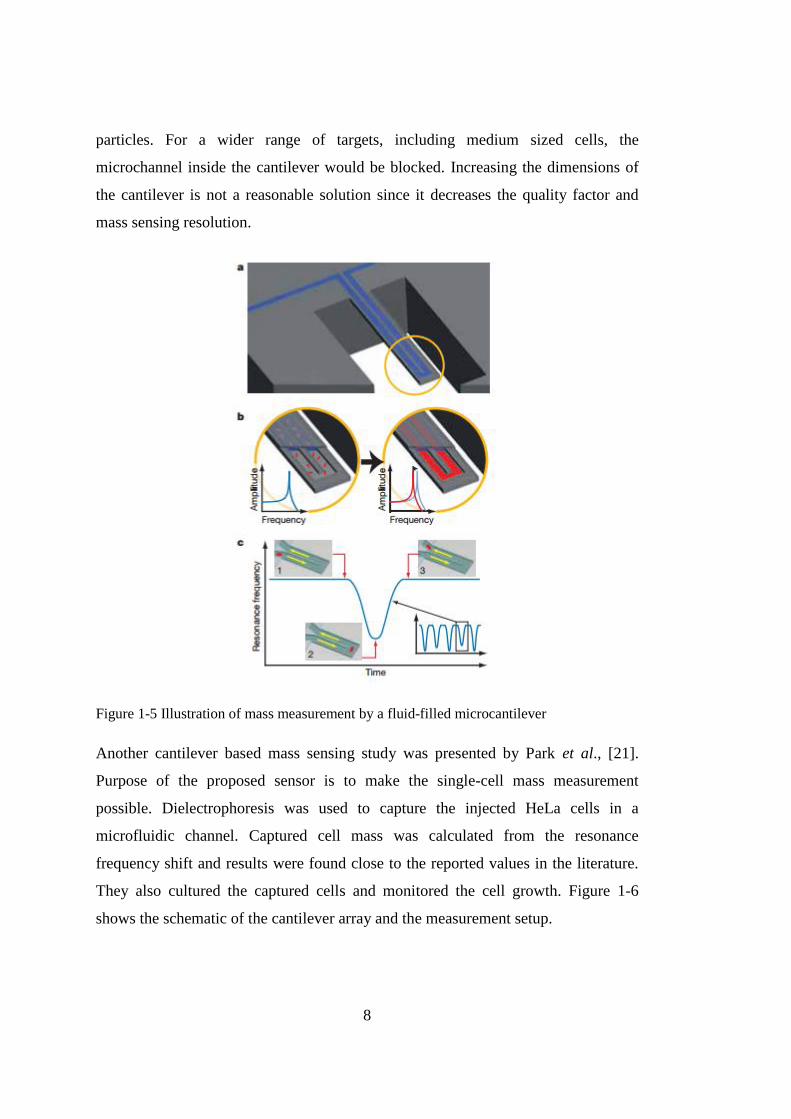
Figure 1-5 Illustration of mass measurement by a fluid-filled microcantilever
Another cantilever based mass sensing study was presented by Park et al., [21].
Purpose of the proposed sensor is to make the single-cell mass measurement
possible. Dielectrophoresis was used to capture the injected HeLa cells in a
microfluidic channel. Captured cell mass was calculated from the resonance
frequency shift and results were found close to the reported values in the literature.
They also cultured the captured cells and monitored the cell growth. Figure 1-6
shows the schematic of the cantilever array and the measurement setup.

9
Figure 1-6 Schematic diagram of living cantilever array. As the captured cells are cultured
on the array, their mass changes are measured using the resonance frequency shift [21].
Proposed sensor in this study not only measures the single-cell mass but also enables
monitoring of the cell growth and analyzes its lifetime. However, requirement of
additional equipment makes it unsuitable for widespread usage in the analysis
laboratories.
Bayraktar et al. reported design, fabrication and test results of MEMS based
gravimetric resonator with lateral motion capability to eliminate the drawbacks of
the traditional cantilever-based detectors [22]. This structure decreases the squeeze
film damping and it is experimentally verified that the system is capable of
achieving 5.91 fg/Hz mass sensitivity by measuring the mass of a single 3 µm
diameter polystyrene bead. One of the key features of the design is parylene coating.
Hydrophobicity of parylene prevents liquid flow through gaps of the sensor and
enables the in-liquid measurements by reducing the slide film damping significantly
[23]. Figure 1-7 shows the design and test results.
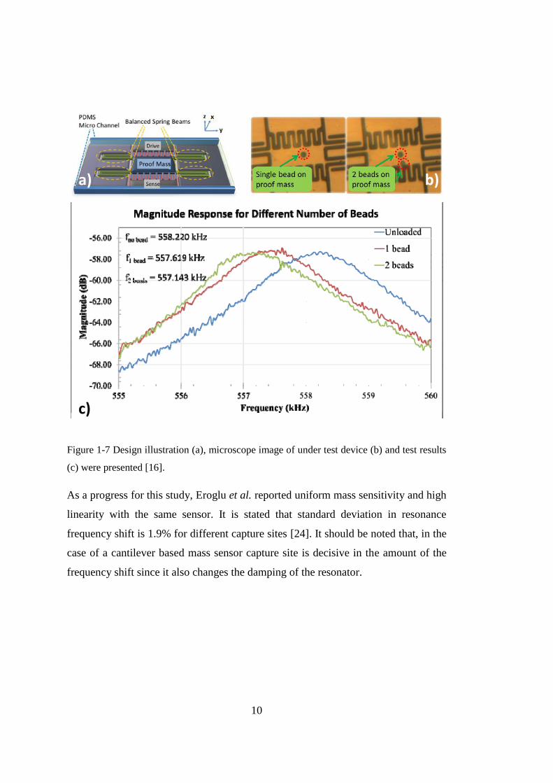
10
Figure 1-7 Design illustration (a), microscope image of under test device (b) and test results
(c) were presented [16].
As a progress for this study, Eroglu et al. reported uniform mass sensitivity and high
linearity with the same sensor. It is stated that standard deviation in resonance
frequency shift is 1.9% for different capture sites [24]. It should be noted that, in the
case of a cantilever based mass sensor capture site is decisive in the amount of the
frequency shift since it also changes the damping of the resonator.
a) b)
c)
11
Figure 1-8 Frequency response for unloaded resonator and different bead locations [24]
Ability of capacitive mass sensing in liquid filled microchannel distinguishes this
work from others. Proposed sensor in [17] is accepted as benchmark design in this
thesis due to its unique characteristics. Even though the advanced properties, it has

12
design issues that prevents the real-time sensing. There is a capacitive crosstalk
between input and output, and the amount of crosstalk electrical current increases
when the microchannel is filled. Since the gain of the proposed sensor is low due to
inefficient capacitive actuation and sensing, crosstalk current (feedthrough current)
prevents the real time sensing as it is an obstacle for the self-oscillation. Reasons
and solutions of the problems of this sensor will be discussed after essential
background theory will be given.
In this section, high-impact examples of gravimetric detection sensors were
introduced. It is seen that although there is a benchmark design that solves some of
the traditional problems of gravimetric devices, it still cannot enable real time in-
liquid cell detection.
1.3 Research Objectives and Thesis Organization
Objectives of the thesis are to solve the issues related with existing gravimetric
sensors in the literature with the capability of real-time mass measurement. To this
end,
increasing the gain by capacitive actuation and sensing optimizations;
decreasing damping while keeping the gain of the transfer function and mass
sensitivity;
eliminating the effect of feedthrough current that prevents the self-oscillation
of the resonator has been selected as the objectives of the thesis.
The thesis is organized as follows:
Chapter 2 gives the essential theoretical background to analyze the operation of
micromechanical resonators. Second order mass, spring, damper system is used for
mathematical analyses of physical resonator. After that, capacitive actuation and
sensing methods are introduced. Next, feedthrough current effect, which is the
primary obstacle of real-time detection, is presented and some elimination methods
are proposed. After the necessary theoretical background, the design procedure of
the devices is presented together with the Comsol finite element analysis results.

13
Chapter 3 is about the fabrication of the resonators. Previous process flow for
fabrication is given and fabrication related problems are analyzed. A new process
flow is proposed to solve the mentioned fabrication problems. Fabrication of the
proposed sensors was established by following the new flow.
Various measurements are presented in chapter 4. First, the experimental setup
including test electronics is briefly given. Then, resonance characterizations of each
design are presented. After, mass detection test procedure and result is introduced.
Finally, resonance characterization of a wet sensor is shown.
Finally, chapter 5 concludes the thesis. Accomplished research objectives and
possible future work suggestions are given.

14

15
CHAPTER 2
2 THEORY & DESIGN
In this chapter, the theoretical background of the resonant based capacitive
gravimetric sensor and the mathematical analysis of the device design procedure are
presented.
Section 2.1 explains the theory behind the operation of the sensor in two parts; the
resonator-by utilizing a second order mass, spring, damper model-and the capacitive
actuation and sensing. This section also introduces the reasons and the effects of the
feedthrough current. Section 2.2 gives the device structures with the design
parameters and the design procedure.
2.1 Working Principles of a Resonant Based Capacitive Gravimetric Sensor
A resonant based sensor can be analyzed under two subtopics. The first one is the
mechanical resonator. It simply converts the applied force to displacement. The
second subtopic contains the actuation and the sensing mechanisms. The actuation is
the part that converts the applied input to the force that is necessary to make the
resonator move. On the other hand, the sense part transforms the displacement of the
resonator into a detectable parameter.
In a resonant based capacitive gravimetric sensor (RCGS), applied electrical
potential is the input that is converted to the force (actuation), this force creates a
displacement on a suspended mass (resonator), and finally the displacement is
converted to the electrical current (sensing) that can be sensed by proper electronics.
Theory of the resonator is given in section 2.1.1. Displacement of a resonator under
applied force is investigated. The capacitive actuation and the sensing mechanisms
are analyzed in section 2.1.2 to get the ideal transfer function of a resonant based
16
capacitive gravimetric sensor. To complete the theoretical aspect of the resonant
based capacitive sensor, feedthrough current should also be investigated. In a
capacitive actuation and sensing there is an inevitable stray current directly between
the actuation and the sense parts which is named as feedthrough current. Section
2.1.3 explains the effect of the feedthrough current in detail.
2.1.1 Resonator Theory
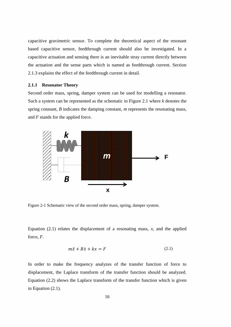
Second order mass, spring, damper system can be used for modelling a resonator.
Such a system can be represented as the schematic in Figure 2.1 where k denotes the
spring constant, B indicates the damping constant, m represents the resonating mass,
and F stands for the applied force.
Figure 2-1 Schematic view of the second order mass, spring, damper system.
Equation (2.1) relates the displacement of a resonating mass, x, and the applied
force, F.
𝑚�̈� + 𝐵�̇� + 𝑘𝑥 = 𝐹 (2.1)
In order to make the frequency analyzes of the transfer function of force to
displacement, the Laplace transform of the transfer function should be analyzed.
Equation (2.2) shows the Laplace transform of the transfer function which is given
in Equation (2.1).
P-3P-7
P-12P-13
P-14P-15
m
k k
B Bx
F
17
𝑋(𝑠)
𝐹(𝑠)=
1
𝑚𝑠2 + 𝐵𝑠 + 𝑘
(2.2)
Natural frequency of a spring mass system is defined as:
𝜔𝑛 = √𝑘
𝑚
(2.3)
However, natural frequency is not the frequency that system gain has its maximum
value in a damped system. The frequency of oscillation, the frequency that the gain
is the maximum, can be expressed as in Equation (2.4):
𝜔𝑑 = 𝜔𝑛√1 − 𝜉𝑑2
(2.4)
where 𝜉𝑑 represents the damping ratio and it can be defined as:
𝜉𝑑 =𝐵
2√𝑚𝑘 .
(2.5)
Damping ratio is an important parameter especially for the self-oscillation. If the
damping ratio is greater than 1, then oscillation frequency becomes an imaginary
number which means oscillation at any frequency cannot be achieved. Such a
system can be named as an overdamped system. On the other hand, if the damping
ratio is less than 1, the system becomes underdamped. Oscillation frequency of an
underdamped system becomes closer to the natural frequency of the system as the
damping ratio decreases further.
In order to measure how much underdamped the system is, there is a parameter
namely quality factor (Q). Quality factor can be defined as:
𝑄 =1
2𝜉𝑑√1 − 𝜉𝑑2
. (2.6)
In this work, lateral resonators are studied and damping ratio of a lateral resonator is
usually smaller than even 0.05 in air. Therefore, Equation (2.6) can be expressed as
follows:
𝑄 ≅1
2𝜉𝑑=
√𝑘𝑚
𝐵 .
(2.7)

18
2.1.2 Electrostatic Capacitive Actuation and Sensing
Mechanical resonator systems in MEMS application can have several types of
actuation and sensing mechanisms such as thermal[25], [26], optic[27], [28],
electrostatic[29] etc. In our case, actuation is handled by electrostatic force and the
displacement of the resonator is sensed by detecting the injected output electrical
current.
The source of electrostatic force on the capacitive plates is the change in the stored
electrostatic energy. Basically, gradient of this energy gives the electrostatic force
on the plates. In order to extract the actuation force, capacitance and stored energy
should be formulized.
The schematic view of a parallel plate capacitor is seen in Figure 2-2 and the total
capacitance of a parallel plate structure is given in Equation (2.7) where 𝜀𝑟 is the
medium relative permittivity, 𝜀0 is the vacuum permittivity, Loverlap is the capacitive
overlap length, h is the plate height and dgap is the distance between the capacitive
plates.

19
Figure 2-2 Schematic view of a parallel plate capacitor with associated variables.
𝐶 = 𝜀𝑟𝜀0
𝐿𝑜𝑣𝑒𝑟𝑙𝑎𝑝 ∗ ℎ
𝑑𝑔𝑎𝑝
(2.7)
Stored electrostatic energy on the capacitive plates is an outcome of the applied
electrical potential. The expression for the electrostatic energy is presented in
Equation (2.8).
𝐸 =1
2𝐶𝑉2
(2.8)
Gap (dgap)
Height (h)
Capacitive overlap length (Loverlap)
20
As it is already stated, force can be extracted by taking the gradient of the
electrostatic energy:
𝐅 = ∇𝐸.
(2.9)
Let’s say that the capacitor plates can only move in the x-axis (the resonators
designed in this thesis have one dominant axes of motion) the electrostatic force
expression reduces to:
𝐅 =∂E
∂x=
1
2
∂C
∂x𝑉2.
(2.10)
Now assume that a voltage that consists of both DC and AC components, as in the
Equation (2.11), is applied to one of the capacitor plates.
𝑉 = 𝑉𝐷𝐶 + 𝑉𝑎𝑐sin (𝜔𝑡) (2.11)
Then, the expression of the electrostatic force becomes as in Equation (2.12).
𝐹 =1
2
∂C
∂x [(𝑉𝐷𝐶
2 +𝑉𝑎𝑐
2
2) + 2𝑉𝐷𝐶𝑉𝑎𝑐 sin(𝜔𝑡) − 𝑉𝑎𝑐
2cos (2𝜔𝑡)] (2.12)
Consider one of the capacitive plates as a surface of movable resonator and the other
one as fixed. Equation (2.12) and Equation (2.1) show that applying only a DC
potential alone would result in movable plate displacement until the spring force and
the electrostatic force become equal. On the other hand, applying an AC potential
introduces two varying force components with angular frequencies of w and 2w. The
force component with the angular frequency of 2w is an unintended side effect and
in order to eliminate the effect of this force, choosing a DC potential which is very
larger than the AC potential is sufficient. Assuming that DC voltage is far greater
than the AC voltage, Equation (2.12) can be simplified as:

21
𝐹 =1
2
∂C
∂x [𝑉𝐷𝐶
2 + 2𝑉𝐷𝐶𝑉𝑎𝑐 sin(𝜔𝑡)]. (2.13)
Proposed resonator has symmetric and stationary sense and drive ports on the
displacement axis. DC voltage is applied to the suspended resonating part and AC
voltage is applied to the stationary actuation part. Therefore, the net force on the
movable part does not have 𝑉𝐷𝐶2 part due to symmetry. The net force on the
suspended part and its Laplace transform can be seen in Equation (2.14) & (2.15)
𝐹𝑥(𝑡) =∂C
∂x𝑉𝐷𝐶𝑉𝑎𝑐 sin(𝜔𝑡) (2.14)
𝐹𝑥(𝑠) =∂C
∂x𝑉𝐷𝐶𝑉(𝑠)
(2.15)
While the electrostatic actuation is caused by a change in the stored energy on the
capacitive plates, the sensing mechanism is based on a change in the stored charge.
Change in the capacitance of the plates crates a change in the stored charge of the
capacitor. As a result of stored charge variance, a current injection through the
capacitor occurs. Therefore the injected current can be formulated as the rate of
change of the stored charge as in Equation (2.16).
𝑖(𝑡) =𝜕𝑄
𝜕𝑡=
𝜕𝐶
𝜕𝑡𝑉 + 𝐶(𝑡)
𝜕𝑉
𝜕𝑡 (2.16)
As previously rationalized 𝑉𝐷𝐶 ≫ 𝑉𝑎𝑐, so the second term in Equation (2.17) can be
neglected and the equation reduces to:
𝑖(𝑡) ≅𝜕𝐶
𝜕𝑡𝑉𝐷𝐶 = (
𝜕𝐶
𝜕𝑥
𝜕𝑥
𝜕𝑡) 𝑉𝐷𝐶 . (2.17)
Laplace transform of the system is also necessary for analyzing the frequency
response of the system:
22
𝐼(𝑠) =𝜕𝐶
𝜕𝑥𝑠𝑋(𝑠)𝑉𝐷𝐶 .
(2.18)
To conclude, applying a voltage that has AC and DC parts creates an electrostatic
force and as a result of this electrostatic force, displacement of the movable part
takes place. Displacement of the capacitive plate is the reason of the capacitance
change and the current injection through the sense part. Therefore, the input of the
system is the applied voltage and the output is the sense current. The overall transfer
function of the system which relates the injected output current to the applied input
voltage can be extracted by multiplying three transfer functions (V to F, F to x, x to
I). Equation (2.19) shows the overall transfer function. A possible frequency
response of Equation (2.19) is given in Figure 2-3.
𝐻𝑡𝑜𝑡𝑎𝑙(𝑠) =𝐼(𝑠)
𝑉(𝑠)=
𝑋(𝑠)
𝐹(𝑠)
𝐹(𝑠)
𝑉(𝑠)
𝐼(𝑠)
𝑋(𝑠)=
𝑠 (∂C∂x
𝑉𝐷𝐶)2
𝑚𝑠2 + 𝑏𝑠 + 𝑘
(2.19)
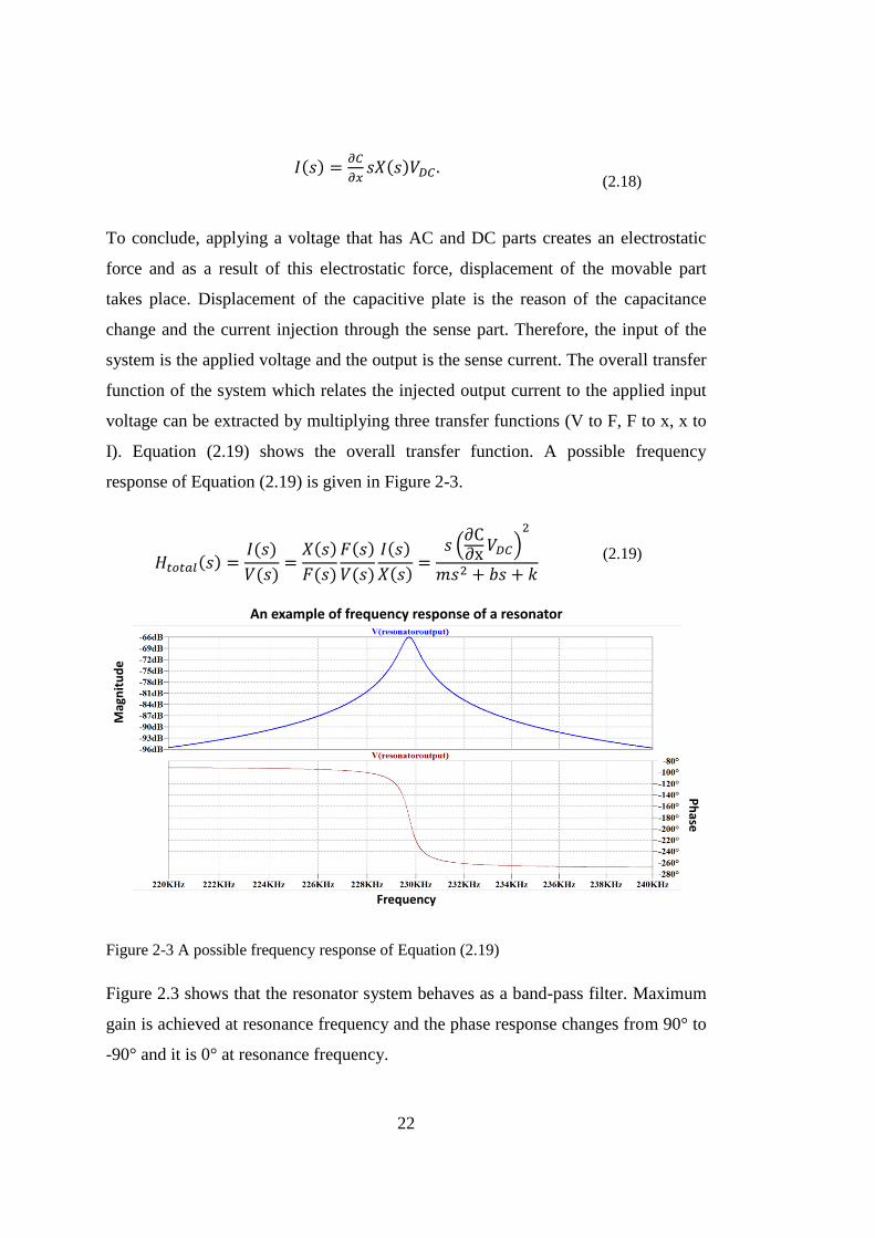
Figure 2-3 A possible frequency response of Equation (2.19)
Figure 2.3 shows that the resonator system behaves as a band-pass filter. Maximum
gain is achieved at resonance frequency and the phase response changes from 90° to
-90° and it is 0° at resonance frequency.
Frequency
Ph
ase
Mag
nit
ud
e
An example of frequency response of a resonator

23
It can be seen from Equation (2.19) that the magnitude of the transfer function is
proportional with the applied DC voltage, 𝑉𝐷𝐶, and the capacitance change with an
infinitesimal displacement on the movement direction, ∂C
∂x. As it is already explained,
capacitance is proportional with the ratio of the capacitive area and gap.
Displacement of a capacitive plate may change the capacitive overlap area and/or
the gap between capacitive surfaces. Therefore capacitive resonators can be
investigated under two categories according to the method of the capacitance
change; varying overlap area and varying gap.
2.1.2.1 Varying overlap area capacitance
In the varying overlap area capacitive actuation, the structure is allowed to move in
such a direction that only the capacitive overlap area of the plates changes with the
displacement. An example of such movement is illustrated in Figure 2-4.
Figure 2-4 Illustration of varying overlap capacitance
dgap
h
Loverlap

24
Illustrated displacement of ∆𝑥 in Figure 2-4 changes the capacitance between the
plates by changing Loverlap. The change in the capacitor with an infinitesimal
displacement of ∆𝑥 is calculated in Equation (2.20).
𝜕𝐶
𝜕𝑥=
𝜕 (𝜀(𝐿𝑜𝑣𝑒𝑟𝑙𝑎𝑝 + ∆𝑥) ∗ ℎ
𝑑𝑔𝑎𝑝)
𝜕𝑥= 𝜀
ℎ
𝑑𝑔𝑎𝑝
(2.20)
Equation (2.20) emphasizes that the length of the capacitor plates has no role in the
capacitive change with displacement. The other result that can be extracted is the
linearity of the capacitance change. Simply, amount of the capacitance change is not
a function of the displacement.
2.1.2.2 Varying gap capacitance
Capacitive structures that are allowed to move in such a direction that only the
distance between capacitive plates changes as it moves are named as varying gap
capacitance. Figure 2-5 displays an example of such a displacement.
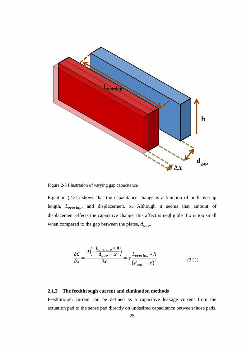
25
Figure 2-5 Illustration of varying gap capacitance
Equation (2.21) shows that the capacitance change is a function of both overlap
length, 𝐿𝑜𝑣𝑒𝑟𝑙𝑎𝑝, and displacement, x. Although it seems that amount of
displacement effects the capacitive change, this affect is negligible if x is too small
when compared to the gap between the plates, 𝑑𝑔𝑎𝑝.
𝜕𝐶
𝜕𝑥=
𝜕 (𝜀𝐿𝑜𝑣𝑒𝑟𝑙𝑎𝑝 ∗ ℎ
𝑑𝑔𝑎𝑝 − 𝑥)
𝜕𝑥= 𝜀
𝐿𝑜𝑣𝑒𝑟𝑙𝑎𝑝 ∗ ℎ
(𝑑𝑔𝑎𝑝 − 𝑥)2
(2.21)
2.1.3 The feedthrough current and elimination methods
Feedthrough current can be defined as a capacitive leakage current from the
actuation pad to the sense pad directly on undesired capacitance between those pads.
dgap
h
Loverlap

26
Magnitude of the feedthrough current continuously increases with frequency since
the impedance of capacitance decreases with frequency. Therefore, magnitude of the
output current becomes greater at higher frequencies than the resonance frequency.
However, it is desired that the output current should be at its maximum value at the
resonance frequency.
In order to analyze the effect of feedthrough current further, feedthrough term
should be added to overall transfer function. Equation (2.22) shows the updated
transfer function that contains feedthrough current term.
𝐻𝑡𝑜𝑡𝑎𝑙(𝑠) =𝐼(𝑠)
𝑉(𝑠)=
𝑠 (∂C∂x
𝑉𝐷𝐶)2
𝑚𝑠2 + 𝑏𝑠 + 𝑘+ 𝑠𝐶𝑓𝑒𝑒𝑑𝑡ℎ𝑟𝑜𝑢𝑔ℎ
(2.22)
At the resonance frequency, mechanical resonance based part of the transfer
function has only real part. Since the feedthrough current is a capacitive current, it
adds only imaginary part to the transfer function. As a result of this situation,
magnitude peak and phase change at resonance is suppressed by the feedthrough
current. Figure 2-6 illustrates the feedthrough current effect on resonance
characteristics.

27
Figure 2-6 Green line denotes the AC response of the resonator only, whereas blue and red
lines show the contribution of feedthrough current on 0.1 fF and 1 fF of capacitance,
respectively.
Barkhausen stability criterion says that closed loop oscillation at a certain frequency
occurs if the phase response of a closed loop system is 0° and magnitude response is
at least 1. Feedthrough effect prevents the closed loop oscillation at resonance
frequency by introducing higher gain for the higher frequencies and by disrupting
the phase response.
In this thesis, two different feedthrough current cancellation techniques are
investigated[30].
Effect of Feedthrough Current on Resonator Characteristic
No feedthrough current
Feedthrough on 0.1 f capacitance
Feedthrough on 1 f capacitance
Frequency
Ph
ase
Mag
nit
ud
e
Ph
ase
Mag
nit
ud
e
28
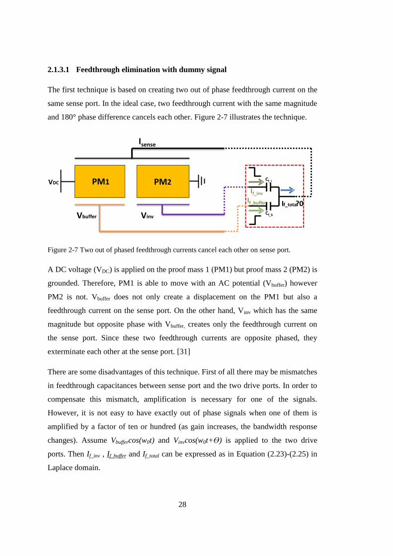
2.1.3.1 Feedthrough elimination with dummy signal
The first technique is based on creating two out of phase feedthrough current on the
same sense port. In the ideal case, two feedthrough current with the same magnitude
and 180° phase difference cancels each other. Figure 2-7 illustrates the technique.
Figure 2-7 Two out of phased feedthrough currents cancel each other on sense port.
A DC voltage (VDC) is applied on the proof mass 1 (PM1) but proof mass 2 (PM2) is
grounded. Therefore, PM1 is able to move with an AC potential (Vbuffer) however
PM2 is not. Vbuffer does not only create a displacement on the PM1 but also a
feedthrough current on the sense port. On the other hand, Vinv which has the same
magnitude but opposite phase with Vbuffer, creates only the feedthrough current on
the sense port. Since these two feedthrough currents are opposite phased, they
exterminate each other at the sense port. [31]
There are some disadvantages of this technique. First of all there may be mismatches
in feedthrough capacitances between sense port and the two drive ports. In order to
compensate this mismatch, amplification is necessary for one of the signals.
However, it is not easy to have exactly out of phase signals when one of them is
amplified by a factor of ten or hundred (as gain increases, the bandwidth response
changes). Assume Vbuffercos(w0t) and Vinvcos(w0t+Ɵ) is applied to the two drive
ports. Then If_inv , If_buffer and If_total can be expressed as in Equation (2.23)-(2.25) in
Laplace domain.
Vbuffer Vinv
PM1 PM2VDC
If_inv
If_buffer If_total?0
Isense
Cf_i
Cf_b

29
𝐼𝑓𝑏𝑢𝑓𝑓𝑒𝑟(𝑠) = 𝑉𝑏𝑢𝑓𝑓𝑒𝑟
𝑠
𝑠2 + 𝑤02 𝑠𝐶𝑓𝑏
= 𝐾𝑏
𝑠2
𝑠2 + 𝑤02
(2.23)
𝐼𝑓𝑖𝑛𝑣(𝑠) = 𝑉𝑖𝑛𝑣
𝑠𝑐𝑜𝑠(𝜃) − 𝑤0 𝑠𝑖𝑛(𝜃)
𝑠2 + 𝑤02 𝑠𝐶𝑓𝑖
= 𝐾𝑖
𝑠2𝑐𝑜𝑠(𝜃) − 𝑠𝑤0 𝑠𝑖𝑛(𝜃)
𝑠2 + 𝑤02
(2.24)
𝐼𝑓𝑡𝑜𝑡𝑎𝑙(𝑠) = (𝐾𝑏 + 𝐾𝑖𝑐𝑜𝑠(𝜃))
𝑠2
𝑠2 + 𝑤02 − 𝐾𝑖
𝑠𝑤0 𝑠𝑖𝑛(𝜃)
𝑠2 + 𝑤02 (2.25)
Now If_total to If_buffer ratio will emphasize the feedthrough elimination success. As
seen in Equation (2.26), in an exact feedthrough cancellation, where Ki is equal to Kb
and Ɵ is 180°, R becomes zero.
𝑅 =𝐼𝑓𝑡𝑜𝑡𝑎𝑙
(𝑠)
𝐼𝑓𝑏𝑢𝑓𝑓𝑒𝑟(𝑠)
│𝑠=𝑗𝑤0= (1 +
𝐾𝑖
𝐾𝑏𝑐𝑜𝑠(𝜃)) + 𝑗
𝐾𝑖
𝐾𝑏𝑠𝑖𝑛(𝜃) (2.26)
Figure 2-8 shows the effect of phase and magnitude mismatches on feedthrough
elimination. Y axis shows the ratio of total feedthrough current to the single drive
feedthrough current, X axis shows the phase difference between the two drive
signals (Ɵ). There are five lines for five different values of signal magnitude ratios
(Ki over Kb).

30
Figure 2-8. Largest effect of the magnitude mismatch is at Ɵ=180° and amount of remaining
current percentage is equal to the deviation percentage. Whereas effect of phase deviation is
maximum at fully matched gain case and remaining current percentage is approximately
three times of deviation percentage of Ɵ from 180°
Ki and Kb consists of capacitor and applied voltage multiplication. In the case of
mismatching feedthrough capacitors, applied voltage should be adjusted to equalize
the Ki and Kb. However, amplifying one of the signals changes the frequency
response of the amplifier which means arranging magnitudes may change the Ɵ. As
a result, setting phase and magnitude of the dummy signal for feedthrough
elimination can be problematic in case of feedthrough capacitance mismatch.
The second disadvantage is the power consumption. There is a signal which has no
role in the actuation of the resonator. Not only the dummy signal but also the
electronics necessary to obtain the dummy signal consumes power that has no
contribution to the actuation of the mass sensing resonator.
150 155 160 165 170 175 1800
0.05
0.1
0.15
0.2
0.25
0.3
0.35
0.4
0.45
0.5=0.85
=0.88
=0.91
=0.94
=0.97
=1
Phase Difference ( )
15% of remains
=0.85
( =180)
47% of remains
=153
=1)
31
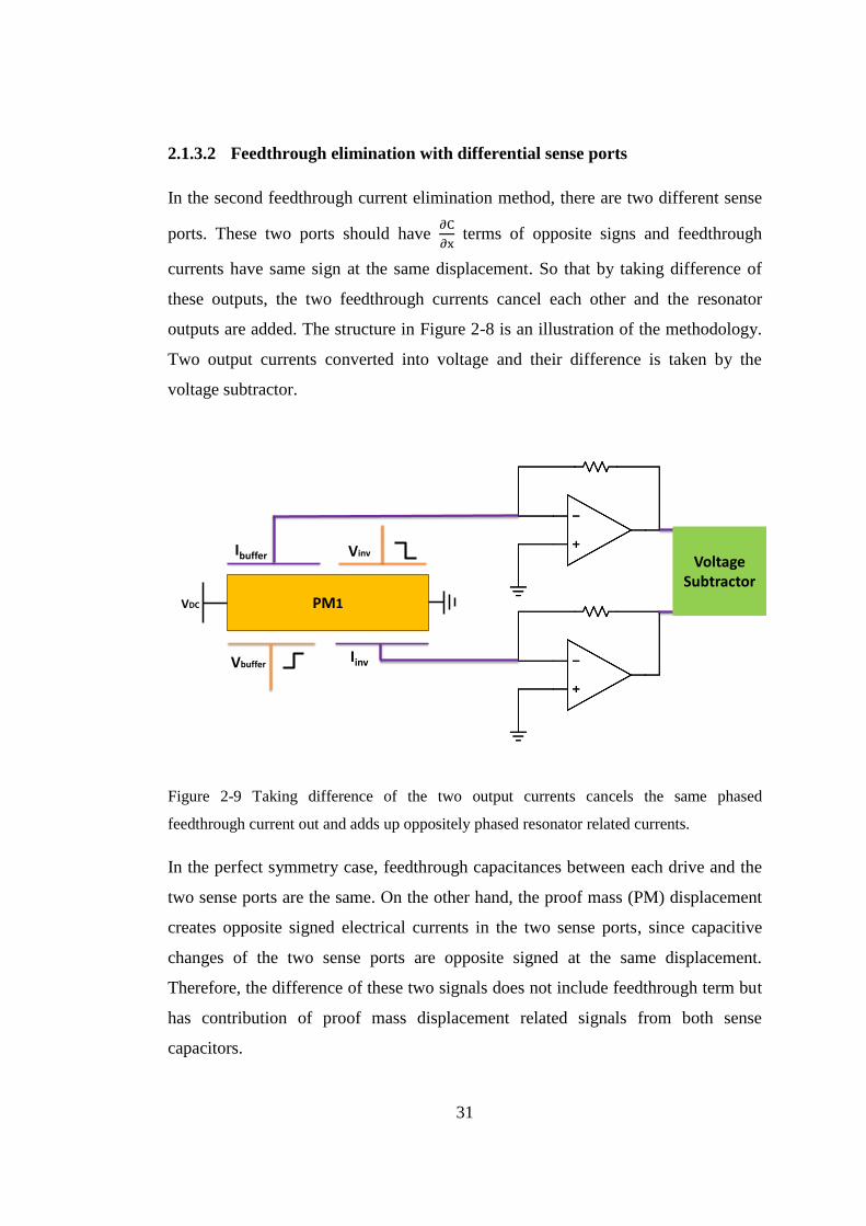
2.1.3.2 Feedthrough elimination with differential sense ports
In the second feedthrough current elimination method, there are two different sense
ports. These two ports should have ∂C
∂x terms of opposite signs and feedthrough
currents have same sign at the same displacement. So that by taking difference of
these outputs, the two feedthrough currents cancel each other and the resonator
outputs are added. The structure in Figure 2-8 is an illustration of the methodology.
Two output currents converted into voltage and their difference is taken by the
voltage subtractor.
Figure 2-9 Taking difference of the two output currents cancels the same phased
feedthrough current out and adds up oppositely phased resonator related currents.
In the perfect symmetry case, feedthrough capacitances between each drive and the
two sense ports are the same. On the other hand, the proof mass (PM) displacement
creates opposite signed electrical currents in the two sense ports, since capacitive
changes of the two sense ports are opposite signed at the same displacement.
Therefore, the difference of these two signals does not include feedthrough term but
has contribution of proof mass displacement related signals from both sense
capacitors.
VDC
Vbuffer
Vinv
PM1
Ibuffer
Iinv
Voltage Subtractor

32
In case of the mismatch in feedthrough capacitances, not the resistance in
transimpedance amplifier but in the voltage subtractor is arranged to adjust the
coefficients in the subtraction. Moreover, unlike the previous method, both signals
are used to actuate the resonator.
2.2 Device Structures and Design Strategies
The resonance frequency of a resonator has an inverse quadratic relation with the
resonating mass. Therefore, added mass can be found by using natural frequencies
of before and after mass addition in Equation (2.27).
∆𝑚 = 𝑘(1
𝑤12 −
1
𝑤22) (2.27)
Variety of resonators with comb finger were designed, fabricated and tested
previously for the purpose of the mass sensing [22], [32], [33]. One of the biggest
design achievements was handled by parylene coating. In order to make the
resonator functional in liquid environment, resonators were parylene coated. Since
parylene is a hydrophobic material, it prevents the liquid flow through to gaps up to
4-5 µm [23].
The most important design trade-off is the necessity of wide surface area to collect
target cells and the request of smaller resonating mass to increase the mass
detectability. These two criteria forces to increase the cell capture surface area to
capacitive surface area ratio. To minimize the resonating mass, active layer of SOI
was also selected as small as possible (5µm is selected since it is the lowest limit for
uniform fabrication). Outcome of these concerns is small output current and the
measurements of the previously designed sensors also showed that the gain of the
transfer function is too small that it can be suppressed by the feedthrough current. In
order to discuss the detailed reasons of this situation, previously designed resonant
based capacitive gravimetric sensor (RCGS#1) will be investigated in section 2.2.1.

33
In order to increase the mass sensing performance of the system, four new resonant
based capacitive gravimetric sensor designs are proposed. The purpose of the
RCGS#2 and RCGS#3 is to increase gain of the resonator without increasing the
total mass of the sensor. Moreover, RCGS#4 and RCGS#5 have the ability of
differential sensing which is designed to eliminate the feedthrough current. For the
sake of design comparison, each design utilizes the same anchor structure (to have
same spring constant) and the first three have the same cell capture area dimensions
with the previously proposed design.
Finite element modeling simulations of each design is also presented. Resonance
frequencies, resonant modes of the sensors including the fundamental one and
displacement amounts are extracted from simulations. Comsol Multiphysics is
employed as simulation tool. Eigenvalue solver of electromechanics physics
interface is used. 100 V and 0 V are selected as boundary conditions for proof mass
and electrodes, respectively, to include stationary electrostatic forces. Ten times
exaggerated displacement at fundamental frequencies are given for each design.
2.2.1 RCGS#1
The first design is one of the previously designed resonators that have comb finger
structure [33]. Before suggesting new device structures, it is important to analyze the
previous one to understand the design drawbacks. In this design, comb finger
structures were presented as capacitive plates. Figure 2-10 shows the illustration of
the sensor. Fundamental vibration mode is presented in Figure 2-11.

34
Figure 2-10 Layout of RCGS#1
Figure 2-11 Fundamental vibration mode of RCGS#1 is at 230 kHz
Direction of displacement is along the finger direction. Therefore, overlap area of
the capacitive plates changes with the displacement. Although the purpose of the
fingers is to create varying overlap area capacitance, there is also a varying gap
Wfinger
dgap
x
Proof
Mass

35
capacitance at fingers ends. While there is a motion, distance between the end of a
finger and the surface across the finger changes. Since the width of the finger is
comparable with the gap between finger ends and across, varying gap capacitive
change is comparable with the varying overlap part. Change of capacitance with
displacement for the varying overlap and varying gap capacitors are calculated to
figure out the contributions of the different capacitive interfaces. Related
calculations can be seen in Equation (2.28) & (2.29). There are 20 fingers in each
side and the length of the finger overlap, Lfinger_overlap, is 42 µm, the gap between
capacitive plates, dgap, is 2 µm, the height of the structure, h, is 5 µm, the length of
the proof mass is equal to 248 µm and the width of the proof mass is 128 µm.
𝜕𝐶
𝜕𝑥=
𝜕 (𝜀(𝐿𝑓𝑖𝑛𝑔𝑒𝑟_𝑜𝑣𝑒𝑟𝑙𝑎𝑝 + 𝑥) ∗ ℎ
𝑑𝑔𝑎𝑝+ 𝜀
(𝑤𝑓𝑖𝑛𝑔𝑒𝑟) ∗ ℎ𝑑𝑔𝑎𝑝 − 𝑥
)
𝜕𝑥
(2.28)
𝜕𝐶
𝜕𝑥= 𝜀
ℎ
𝑑𝑔𝑎𝑝+ 𝜀
(𝑤𝑓𝑖𝑛𝑔𝑒𝑟) ∗ ℎ
(𝑑𝑔𝑎𝑝 − 𝑥)2
(2.29)
The red terms in the equation denote the contribution of varying overlap capacitance
and the black terms refer to varying gap related part.
Overall transfer function includes two ∂C
∂x terms one for sense and the other for
actuation. Note that these two terms differ because of the sign of the displacement,
x.

36
(𝜕𝐶
𝜕𝑥)
𝑠𝑒𝑛𝑠𝑒(
𝜕𝐶
𝜕𝑥)
𝑎𝑐𝑡.
= 𝜀2 (ℎ
𝑑𝑔𝑎𝑝+
(𝑤𝑓𝑖𝑛𝑔𝑒𝑟) ∗ ℎ
(𝑑𝑔𝑎𝑝 − 𝑥)2 ) (
ℎ
𝑑𝑔𝑎𝑝
+ (𝑤𝑓𝑖𝑛𝑔𝑒𝑟) ∗ ℎ
(𝑑𝑔𝑎𝑝 + 𝑥)2 )
(2.30)
Equation (2.30) is calculated with MATLAB for different displacement values and
multiplication of displacement derivatives of capacitive changes at sense and
actuation ports versus displacement is drawn in the Figure 2-12 with the red line.
Moreover, the same multiplication is also calculated and drawn with the
assumptions of there is only varying gap capacitance and only varying overlap
capacitance separately, to see the weight of their contributions. The dashed black
line represents the part that contains only varying gap term and the solid black line
represents the part that contains only varying overlap term.

37
Figure 2-12 (𝜕𝐶
𝜕𝑥)
𝑠𝑒𝑛𝑠𝑒(
𝜕𝐶
𝜕𝑥)
𝑎𝑐𝑡.vs displacement for RCGS#1 is drawn where the red line shows
the total result, the dashed black line is the contribution of only varying gap related term
and the solid black line is the contribution of only varying overlap related term.
Calculation results show that varying gap is far more effective while comparing
varying overlap due to the small gap at the ends of the fingers. To decrease the
varying gap effect, the gap between the finger end and the opposite plate should be
increased. Figure 2.13 shows the overall total capacitive sensitivity versus
displacement for different gaps at fingers ends.
0 0.1 0.2 0.3 0.4 0.5 0.6 0.7 0.8 0.9 10
5
10
15
Proof mass displacement ( m )
Sen
sit
ivit
y (
(n
F/m
)2 )
Varying overlap
Varying gap
Total

38
Figure 2-13 (𝜕𝐶
𝜕𝑥)
𝑠𝑒𝑛𝑠𝑒(
𝜕𝐶
𝜕𝑥)
𝑎𝑐𝑡.vs displacement of RCGS#1 for different gaps at finger ends
In order to make the sensor behave as varying overlap capacitance, gap after finger
end should be wider than 5µm. However, parylene hydrophobicity cannot prevent
liquid flow through the gaps wider than 5µm. There is also a significant drop at the
sensitivity for larger widths.
To conclude, it is seen that contribution of the comb finger to the sensitivity is
limited in this design. Therefore, fingers removal to have fully varying gap
capacitive interface is chosen as the first design idea.
2.2.2 RCGS#2
Calculations in the previous part showed that impact of fingers to the sensitivity is
not very strong. Apart from this, fingers increase damping by increasing the surface
area against the movement [34]. Adding extra mass is another drawback for the
mass sensitivity.
0 0.1 0.2 0.3 0.4 0.5 0.6 0.7 0.8 0.9 10
5
10
15
Proof mass displacement ( m )
Sen
sit
ivit
y (
(n
F/m
)2 )
Gap = 2 m
Gap = 5 m
Gap = 10 m

39
Figure 2-14 shows the proposed resonator which has the same anchor and proof
mass structure with the RCGS#1.
Figure 2-14 Resonator without finger
Fundamental vibration mode is presented in figure 2-15.
Figure 2-15 Fundamental vibration mode of RCGS 1 is at 290 kHz

40
Equation (2.31) expresses the change of capacitance with displacement.
𝜕𝐶
𝜕𝑥=
𝜕 (𝜀𝐿𝑠𝑖𝑑𝑒 ∗ ℎ𝑑𝑔𝑎𝑝 − 𝑥
)
𝜕𝑥= 𝜀
𝐿𝑠𝑖𝑑𝑒 ∗ ℎ
(𝑑𝑔𝑎𝑝 − 𝑥)2
(2.31)
Since the overall transfer function includes two ∂C
∂x terms, one for sense and the other
for actuation Equation (2.32) is used for the representation of capacitive sensitivity.
(𝜕𝐶
𝜕𝑥)
𝑠𝑒𝑛𝑠𝑒∗ (
𝜕𝐶
𝜕𝑥)
𝑎𝑐𝑡. = 𝜀2 (𝜀
𝐿𝑠𝑖𝑑𝑒 ∗ ℎ
(𝑑𝑔𝑎𝑝 − 𝑥)2) ∗ (𝜀
𝐿𝑠𝑖𝑑𝑒 ∗ ℎ
(𝑑𝑔𝑎𝑝 + 𝑥)2)
(2.32)
Equation (2.32) is calculated and the result is compared with the result of RCGS#1.
Figure 2-16 combines the results in the same graphics. The red line denotes the
result of the RCGS#1 and the blue line denotes the RCGS#2.

41
Figure 2-16 (𝜕𝐶
𝜕𝑥)
𝑠𝑒𝑛𝑠𝑒(
𝜕𝐶
𝜕𝑥)
𝑎𝑐𝑡.vs displacement is drawn for RCGS#1 (the red line) and
RCGS#2 (the blue line).
Figure 2-16 shows that finger removal decreases the capacitive sensitivity around
only 3% for the same displacement. Please note that, the total mass of the sensor and
the damping factor is decreased, too. To see the overall effect, gain of transfer
functions of RCGS#1 and RCGS#2 versus frequency is drawn in Figure 2-17 in
MATLAB.
7.94
7.68

42
Figure 2-17 Overall transfer function for resonator with no finger (the red line) and
resonator with comb finger (the blue line)
It can be seen from Figure 2-17 that the resonance frequency, the peak gain at
resonance frequency and the quality factor is increased.
2.2.3 RCGS#3
Analysis of the first two designs shows that the comb fingers do not improve the
output current magnitude but they increase the mass and the damping. If it is
possible to use the removed finger in such an orientation to increase the varying gap
area, an increase in gain will be achieved without any decrease in the resonance
frequency or quality factor. This achievement will also reduce the effect of the
feedthrough current by simply increasing the resonator current to feedthrough
current ratio.
Figure 2-18 illustrates the proposed design. All of the four sides of the resonating
structure are employed to place the fingers. The finger structures are placed so that
the gap between the fingers changes with the displacement. Finger dimensions are
selected so that to make them have the same weight with the fingers of RCGS#1.
While a finger getting close to one of its neighbor fingers, it also moves away from
its other neighbor. Therefore displacement creates two opposite signed current at
two neighbor finger that cancel each other. In order to prevent this effect, one of the
100 120 140 160 180 200 220 240 260 280 300-210
-200
-190
-180
-170
-160
-150
-140
-130
Frequency (KHz)
Mag
nit
ud
e (
dB
)
(Isense/Vdrive) for Infinitesimal Displacements
100 120 140 160 180 200 220 240 260 280 300
-80
-60
-40
-20
0
20
40
60
80
Frequency (KHz)
Ph
ase (
deg
rees)
comb finger case
no finger case
fo1 fo2

43
gaps is selected as three times of the other one and it is called anti-gap. Since the
square of the gap is important and anti-gap to gap ratio is three, only 1/9 of the
current is lost. The ratio is upper bounded by liquid flow protection of parylene
(parylene coating prevents the liquid flow through a gap of upon 4-5 µm [23]. The
gap between the fingers (dgap) is chosen as 1.5µm and the anti-gap (danti_gap) as
4.5µm.
Figure 2-18 Resonator with tree structured finger
Fundamental vibration mode of the sensor is illustrated in figure 2-19.

44
Figure 2-19 Fundamental vibration mode of RCGS 1 is at 239 kHz
Equations (2.33)-(2.35) show the transfer function calculations. There are 30 fingers
at tree structured finger branch with an overlap length of (Lf_overlap_2) 30 µm and 9
fingers at each side with an overlap length (Lf_overlap_1) of 40µm.
𝜕𝐶
𝜕𝑥=
𝜕 (𝜀𝐿𝑓_𝑜𝑣𝑒𝑟𝑙𝑎𝑝_1 ∗ ℎ
𝑑𝑔𝑎𝑝 − 𝑥∗ 30 + 𝜀
𝐿𝑓_𝑜𝑣𝑒𝑟𝑙𝑎𝑝_2 ∗ ℎ𝑑𝑔𝑎𝑝 − 𝑥
∗ 9)
𝜕𝑥∗ (1 − (
𝑑𝑔𝑎𝑝
𝑑𝑎𝑛𝑡𝑖−𝑔𝑎𝑝)
2)
(2.33)
𝜕𝐶
𝜕𝑥= (𝜀
𝐿𝑓𝑜𝑣𝑒𝑟𝑙𝑎𝑝1∗ ℎ ∗ 30
(𝑑𝑔𝑎𝑝 − 𝑥)2 + 𝜀
𝐿𝑓𝑜𝑣𝑒𝑟𝑙𝑎𝑝2∗ ℎ ∗ 9
(𝑑𝑔𝑎𝑝 − 𝑥)2 ) ∗ (1 − (
𝑑𝑔𝑎𝑝
𝑑𝑎𝑛𝑡𝑖−𝑔𝑎𝑝)
2)
(2.34)
(𝜕𝐶
𝜕𝑥)
𝑠𝑒𝑛𝑠𝑒∗ (
𝜕𝐶
𝜕𝑥)
𝑎𝑐𝑡.
= 𝜀2 ∗ (1 − (𝑑𝑔𝑎𝑝
𝑑𝑎𝑛𝑡𝑖−𝑔𝑎𝑝)
2)2 ∗ (
𝐿𝑓𝑜𝑣𝑒𝑟𝑙𝑎𝑝1∗ ℎ ∗ 30
(𝑑𝑔𝑎𝑝 − 𝑥)2 +
𝐿𝑓𝑜𝑣𝑒𝑟𝑙𝑎𝑝2∗ ℎ ∗ 9
(𝑑𝑔𝑎𝑝 − 𝑥)2 )
∗ (𝐿𝑓𝑜𝑣𝑒𝑟𝑙𝑎𝑝1
∗ ℎ ∗ 30
(𝑑𝑔𝑎𝑝 + 𝑥)2 +
𝐿𝑓𝑜𝑣𝑒𝑟𝑙𝑎𝑝2∗ ℎ ∗ 9
(𝑑𝑔𝑎𝑝 + 𝑥)2 )
(2.35)
45
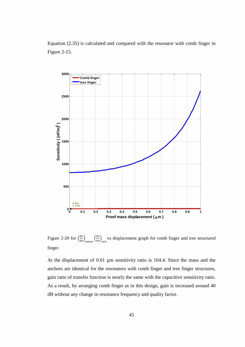
Equation (2.35) is calculated and compared with the resonator with comb finger in
Figure 2-15.
Figure 2-20 for (𝜕𝐶
𝜕𝑥)
𝑠𝑒𝑛𝑠𝑒(
𝜕𝐶
𝜕𝑥)
𝑎𝑐𝑡.vs displacement graph for comb finger and tree structured
finger.
At the displacement of 0.01 µm sensitivity ratio is 104.4. Since the mass and the
anchors are identical for the resonators with comb finger and tree finger structures,
gain ratio of transfer function is nearly the same with the capacitive sensitivity ratio.
As a result, by arranging comb finger as in this design, gain is increased around 40
dB without any change in resonance frequency and quality factor.
0 0.1 0.2 0.3 0.4 0.5 0.6 0.7 0.8 0.9 10
500
1000
1500
2000
2500
3000
X: 0.01
Y: 7.772
Sen
sit
ivit
y (
(n
F/m
)2 )
Proof mass displacement ( m )
Comb finger
tree finger
46
40 dB increments in gain should also decrease the feedthrough effect by increasing
the displacement related output current to feedthrough current ratio by 100 times.
2.2.4 RCGS#4
Apart from boosting the output current of the sensor, decreasing the feedthrough
current is also a good method that can be applied to eliminate the drawbacks of the
feedthrough effect. In the section 2.1.3 two different feedthrough current elimination
methods are described. In this design, the second method is used.
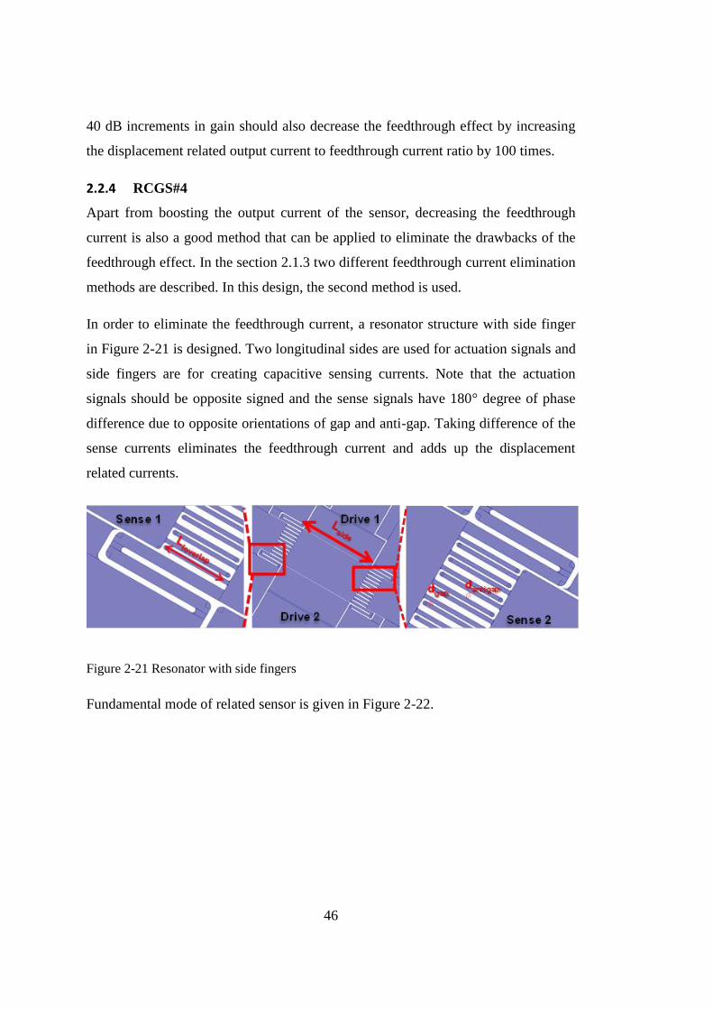
In order to eliminate the feedthrough current, a resonator structure with side finger
in Figure 2-21 is designed. Two longitudinal sides are used for actuation signals and
side fingers are for creating capacitive sensing currents. Note that the actuation
signals should be opposite signed and the sense signals have 180° degree of phase
difference due to opposite orientations of gap and anti-gap. Taking difference of the
sense currents eliminates the feedthrough current and adds up the displacement
related currents.
Figure 2-21 Resonator with side fingers
Fundamental mode of related sensor is given in Figure 2-22.

47
Figure 2-22 Fundamental vibration mode of RCGS 1 is at 257.9 kHz
Let’s derive the transfer function of the sensor:
𝐻𝑡𝑜𝑡𝑎𝑙(𝑠) =𝐼(𝑠)
𝑉(𝑠)=
𝑠(𝑉𝐷𝐶)2(𝜕𝐶𝜕𝑥
)𝑠𝑒𝑛𝑠𝑒(𝜕𝐶𝜕𝑥
)𝑑𝑟𝑖𝑣𝑒
𝑚𝑠2 + 𝑏𝑠 + 𝑘
(2.36)
(𝜕𝐶
𝜕𝑥 )
𝑎𝑐𝑡.= 2 ∗ 𝜀
𝐿𝑠𝑖𝑑𝑒 ∗ ℎ
(𝑑𝑔𝑎𝑝 − 𝑥)2
(2.37)
(𝜕𝐶
𝜕𝑥 )
𝑠𝑒𝑛𝑠𝑒= 2 ∗ ( 𝜀
𝐿𝑓𝑜𝑣𝑒𝑟𝑙𝑎𝑝∗ ℎ ∗ 9
(𝑑𝑔𝑎𝑝 − 𝑥)2 ) ∗ (1 − (
𝑑𝑔𝑎𝑝
𝑑𝑎𝑛𝑡𝑖−𝑔𝑎𝑝)
2
)
(2.38)
Thanks to side fingers, RCGS#4 has higher gain than the RCGS#1 and RCGS#2.
Although it has less gain than RCGS#3, damping and mass of this resonator is
smaller.

48
2.2.5 RCGS#5
It is mentioned that finger structures increases the damping by increasing the
resistive surface against the movement direction. In order to improve the resonator
with side fingers in terms of damping (quality factor and mass sensitivity), a sensor
without finger structure is also designed.
The feedthrough current elimination method used in RCGS#4 needs four different
ports where two of them are for the sense and two of them are for the actuation.
Moreover, the displacement of the resonator must create opposite signed capacitive
change on the sense ports.
Creating a varying gap capacitive interface by tilting the right and left edges of the
moving part, as it is seen in the Figure (2-23), is the proposed design solution. Please
note that, suspended mass moves away from one tilted sense electrode as it gets
closer to the other sense electrode. This is the reason of the opposite signed
capacitive change at the two sense ports.
Figure 2-23 Diamond shaped resonator
Fundamental mode of RCGS4 is given in Figure 2-24.
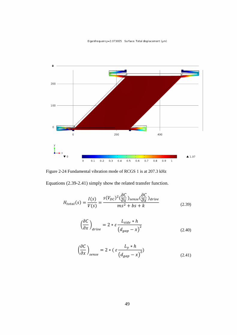
49
Figure 2-24 Fundamental vibration mode of RCGS 1 is at 207.3 kHz
Equations (2.39-2.41) simply show the related transfer function.
𝐻𝑡𝑜𝑡𝑎𝑙(𝑠) =𝐼(𝑠)
𝑉(𝑠)=
𝑠(𝑉𝐷𝐶)2(𝜕𝐶𝜕𝑥
)𝑠𝑒𝑛𝑠𝑒(𝜕𝐶𝜕𝑥
)𝑑𝑟𝑖𝑣𝑒
𝑚𝑠2 + 𝑏𝑠 + 𝑘
(2.39)
(𝜕𝐶
𝜕𝑥 )
𝑑𝑟𝑖𝑣𝑒= 2 ∗ 𝜀
𝐿𝑠𝑖𝑑𝑒 ∗ ℎ
(𝑑𝑔𝑎𝑝 − 𝑥)2
(2.40)
(𝜕𝐶
𝜕𝑥 )
𝑠𝑒𝑛𝑠𝑒= 2 ∗ ( 𝜀
𝐿𝑦 ∗ ℎ
(𝑑𝑔𝑎𝑝 − 𝑥)2)
(2.41)

50
For the sake of symmetry, length and width of the proof mass are chosen as the
same length with the previous resonators. Therefore, the mass of the resonator is
approximately twice of the resonator without finger.
2.2.6 Design Procedure Summary
It is inevitable for design of the proposed gravimetric sensor to have a wide surface
area for cell capturing. It is also straightforward that the mass of the sensor should
be as small as possible to increase the mass sensibility. These two design criteria
limits the surface area of the sense and drive capacitances. Therefore, an
optimization to increase the effectiveness of the capacitive surface has been done.
Another important issue that is considered during the design procedure is the
feedthrough current. To eliminate the feedthrough current two methods were
investigated.
In order to show the validity of the theoretical work experimentally, four new
sensors were designed. Purpose of the RCGS#2 is to show that the comb fingers of
the previously proposed sensor do not contribute to actuation and sensing
significantly but decrease the mass sensitivity by increasing the mass and damping.
RCGS#3 is proposed to show that by just changing the orientation of the finger
mass, it is possible to increase the gain almost two orders of magnitude. By
increasing the output current, it is aimed to reduce the effect of feedthrough current
and make self-oscillation feasible. RCGS#3 and RCGS#4 have two differential
sense ports to eliminate the feedthrough current. RCGS#3, that employs side fingers,
has anchor symmetry of both on x and y axis whereas RCGS#4, diamond shaped
resonator, has only one axis symmetry. On the other hand, RCGS#4 has less
damping due to lacking of the fingers.
Table 2.1 compares the four new designs and one previous design in terms of mass,
resonance frequency, quality factor and gain at resonance frequency. It is purposely
avoided to give specific numbers related with fabricated sensor in comparison chart.
Condition of having same proof mass and anchor dimensions (only the diamond

51
shaped resonator has larger proof mass) is enough for the correctness of the
following table.
Table 2-1 Important parameters of different resonator designs.
Sensor Mass Resonance
Frequency
Quality
Factor
Max.
Gain
Sense
Type
RCGS#1 m f Q G Single
RCGS#2 <m >f >>Q ~G Single
RCGS#3 m f Q >>G Single
RCGS#4 <m >f >Q >>G Differential
RCGS#5 ~2m <f >>Q >G Differential
In the next chapter fabrication process of the designed sensor is investigated.

52
53
CHAPTER 3
3 FABRICATION
In this chapter, the microfabrication methods and process flow of the cell detection
device are presented. There have been several process flows for different
generations of resonators during the studies conducted for the resonant based cell
detection sensors in BioMEMS group [22], [32], [33]. In this thesis the previous
generation process flow is utilized due to its high mechanical yield [33]. Besides, a
newly developed process flow is presented to solve the problems encountered during
the previous generation fabrication is presented.
Proposed process flows employ the SOI (Silicon-on-Insulator) technology, glass
micromachining, wafer bonding, and polymer micromachining.
3.1 Previous Generation Process Flow
Figure 3.1 shows the previous fabrication process flow which is the base of the
newly proposed process flow in the scope of this thesis [33].
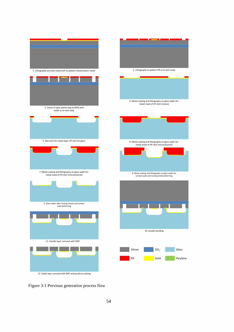
54
Figure 3-1 Previous generation process flow
Silicon SiO2 Glass
PR Gold Parylene
1. Lithography and wet metal etch to pattern bioactivation metal 2. Lithography to pattern PR as Si etch mask
3. Active Si layer patterning by DRIE withoxide as an etch stop
4. Metal coating and lithography on glass wafer for metal mask of HF etch (recess)
5. Wet etch for metal layer, HF etch for glass 6. Metal coating and lithography on glass wafer for metal mask of HF etch (microchannel)
7. Metal coating and lithography on glass wafer for metal mask of HF etch (microchannel)
8. Metal coating and lithography on glass wafer for contact pads and routing metal patterning
9. Glass wafer after routing metals and contact pads patterning
10. Anodic bonding
11. Handle layer removal with DRIE
12. Oxide layer removal with BHF and parylene coating

55
In the previous generation fabrication flow, the resonators were fabricated with the
two wafers; SOI (Silicon-on-Insulator) wafer for the resonator structures and the
glass wafer to form the microchannel and a base for the suspended resonators.
SOI wafer which is used to form the structural layer; has a structural silicon layer
thickness of 5 µm, oxide thickness of 2 µm, and handle layer thickness of 350 µm.
The SOI process starts with the Cr/Au deposition (30nm/300nm) on the structural
silicon layer. Deposited Cr/Au is wet etched with the commercial etchants to pattern
the bioactivation area. The next step of the SOI process is Deep Reactive Ion
Etching (DRIE). DRIE is chosen as it is an anisotropic etching method for the
silicon and enables creating sharp vertical structures. Besides this, oxide layer of the
SOI wafer behaves as an etch stop layer for DRIE. Although oxide is an etch stop
layer, time optimization is still important to prevent the “notching” effect.
Microposit S-1813 type photoresist is used as the masking layer in both Cr/Au
etching and DRIE processes. The purpose of using this photoresist is to have
relatively small deposition thickness (~1.5 µm at 4000 rpm). In order to produce
critical dimensions around 1 to 2 µm having thin photoresist layers is essential. It is
also important that before photoresist coating, the wafer should be dehydrated and
exposed to nitrogen flow in desiccators to improve surface adhesion. Figure 3-2
shows the microscope image after the SOI process is finished.

56
Figure 3-2 Microscope image of the resonator site of the SOI wafer
Glass wafer is processed in parallel with the SOI wafer process. Fabrication flow on
the glass wafer starts with Cr/Au sputtering and patterning. Metal layers serve as a
mask for pure Hydrofluoric acid (HF) wet glass etching. Similar with SOI process,
metal is patterned with commercial wet etchants after photolithography. When the
mask is ready, glass wafer is etched with pure HF to form the recess gap. Photoresist
and metal layers are stripped of once wet HF etch is finished.
Glass wafer is etched to shape cavities for both recess gap of metal routings and
resonators, and microchannel consecutively with different masks. These two
etchings are done separately since the depth of the gaps is different. Therefore, the
same steps are repeated for the microchannel gap, only HF etch time of recess gap is
longer.
When glass etchings finished, wafer is coated with Cr/Au (30nm/300nm) to pattern
metal routing lines and contact pads. Photolithography of the second metal mask and
metal routing lines is done with a photoresist with high film thickness (spray coating
Drive
Sense
Pro
of
mas
s
Ce
ll ca
ptu
re
area
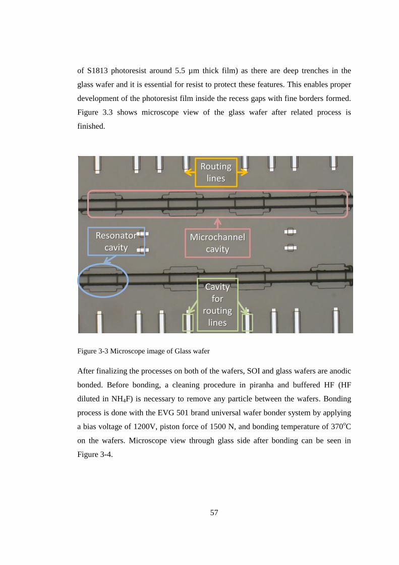
57
of S1813 photoresist around 5.5 µm thick film) as there are deep trenches in the
glass wafer and it is essential for resist to protect these features. This enables proper
development of the photoresist film inside the recess gaps with fine borders formed.
Figure 3.3 shows microscope view of the glass wafer after related process is
finished.
Figure 3-3 Microscope image of Glass wafer
After finalizing the processes on both of the wafers, SOI and glass wafers are anodic
bonded. Before bonding, a cleaning procedure in piranha and buffered HF (HF
diluted in NH4F) is necessary to remove any particle between the wafers. Bonding
process is done with the EVG 501 brand universal wafer bonder system by applying
a bias voltage of 1200V, piston force of 1500 N, and bonding temperature of 370oC
on the wafers. Microscope view through glass side after bonding can be seen in
Figure 3-4.
Routing lines
Resonator cavity
Microchannel cavity
Cavity for
routing lines

58
Figure 3-4 Microscope view through glass wafer after anodic bonding
In order to release the resonators, handle and oxide layers of the SOI wafer should
be removed. DRIE is used for removal of the handle layer of the SOI wafer. After
that, the oxide layer is etched with BHF solution (1:5). In order to remove the BHF,
wafer is cleaned in DI water for a long time. Vaporization of water is harmful for the
suspended resonators due to surface tension. Instead of vaporizing, drying process is
done by bathing the resonator in the order of acetone, isopropyl alcohol (IPA), and
methanol. As a last step of drying, methanol is vaporized on a hot plate at 70°C.
The last part of the fabrication is parylene layer coating with CVD. Wafer is coated
with 0.5µm of Parylene-C. During deposition, parylene vapor flows through all gaps
and coats the whole surfaces including sides of fingers and top and bottom of the
resonator. However, parylene is not desired on top of the bioactivation gold to make
surface activation for selective cell capture possible to direct contact with the gold
layer. To etch the parylene on bioactivation gold, wafer is placed inside oxygen
plasma for an optimized short period . Parylene thickness is thinner inside the
Routing lines
Resonator cavity Microchannel
cavity
Cavity for
routing lines
Contact points between routing lines and Si
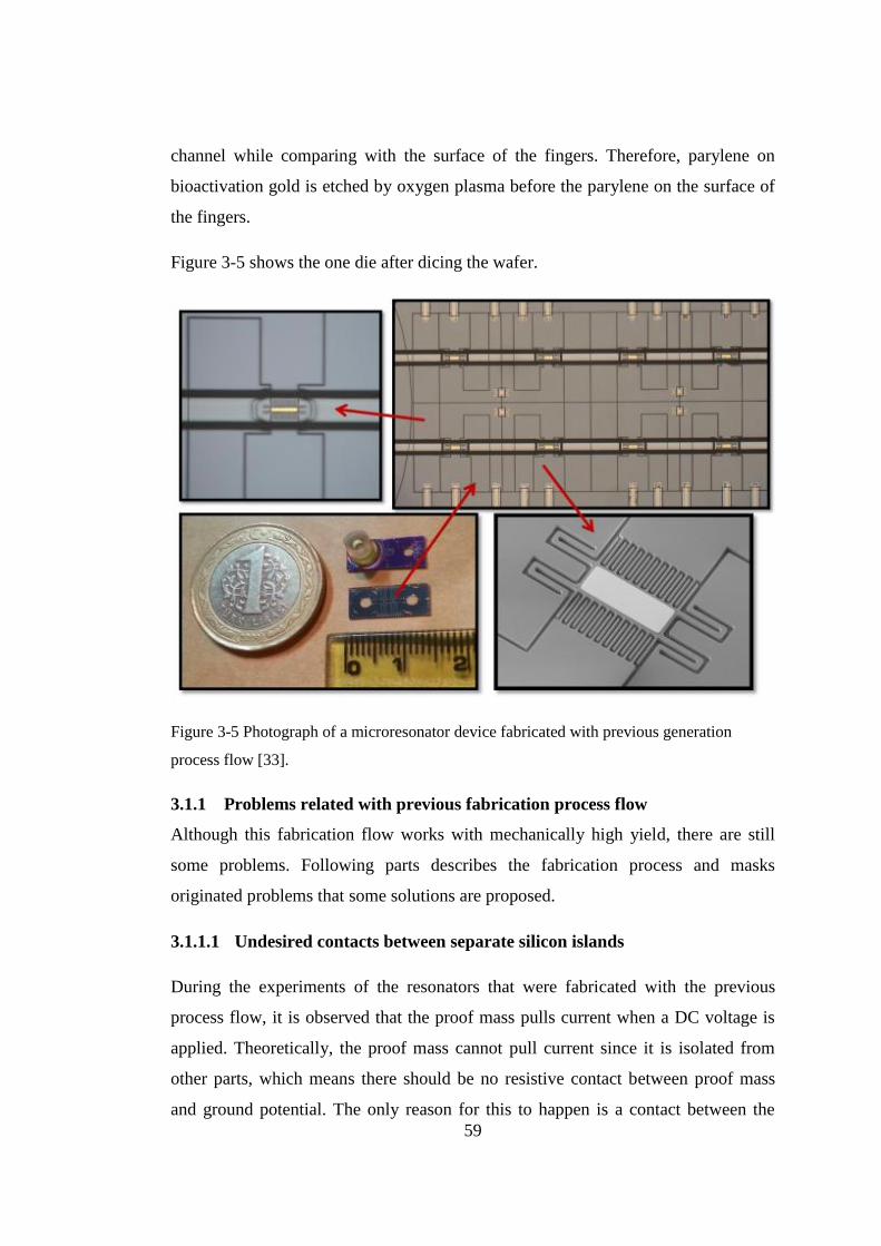
59
channel while comparing with the surface of the fingers. Therefore, parylene on
bioactivation gold is etched by oxygen plasma before the parylene on the surface of
the fingers.
Figure 3-5 shows the one die after dicing the wafer.
Figure 3-5 Photograph of a microresonator device fabricated with previous generation
process flow [33].
3.1.1 Problems related with previous fabrication process flow
Although this fabrication flow works with mechanically high yield, there are still
some problems. Following parts describes the fabrication process and masks
originated problems that some solutions are proposed.
3.1.1.1 Undesired contacts between separate silicon islands
During the experiments of the resonators that were fabricated with the previous
process flow, it is observed that the proof mass pulls current when a DC voltage is
applied. Theoretically, the proof mass cannot pull current since it is isolated from
other parts, which means there should be no resistive contact between proof mass
and ground potential. The only reason for this to happen is a contact between the

60
proof mass and the other ports that are DC-grounded. In order to understand the
place of the contact, laser cutter is used. Cr/Au lines were cut at the edges of the
each separate silicon island. After cutting the lines at the edges of the drive, sense,
and proof mass parts, current on proof mass was disappeared. This result shows that
there are some particles inside the recess gaps that create a resistive path through
metal line to substrate silicon. Figure 3.6 shows the contact point of gold lines to the
proof mass, sense and drive parts of the resonator and the part that broken with laser
cutter.
Figure 3-6 Gold lines in recess gap creates undesired resistive path between Si islands.
Yellow rectangles show the parts that would be broken by laser cutter in order to prevent
proof mass current leakage.
3.1.1.2 High feedthrough current
As described in chapter 2, high feedthrough current causes operational troubles.
Results of tests conducted on the resonators fabricated with the previous flow shows
that the feedthrough capacitance is about 50 fF, which causes relatively high current
on high frequencies. As seen from the Figure 3-7, contact pads for drive and sense
ports of a resonator is on the same side of the die. Since wirings of these two ports
are very close to each other, a high feedthrough capacitance is formed between
them.
Before the laser cut
After the laser cut
Bulk Si
Si&Au contact points
Where Au line will be cut

61
Figure 3-7 Illustration of feedthrough capacitor on resonator
3.2 New Generation Process Flow
To overcome the problems related with the previous generation fabrication flow, a
modified process flow with the new mask set was proposed. In this flow, metal
routings are removed from the inside of the recess gaps of glass wafer to prevent the
contacts between separate silicon islands. Moreover, the orientation of the contact
pads is changed to reduce the feedthrough current. Figure 3-8 illustrates the process
flow.
PR
OF
MA
SSSENSE
DRIVE
CFeedthrough

62
Figure 3-8 New generation fabrication flow
The fabrication process of the SOI wafer starts with the bioactivation Cr/Au
(30nm/300nm) deposition and the SOI patterning with DRIE as in the previous
generation process flow. However, in this case silicon islands of drive, sense, and
proof mass continues until contact pad area. Note that in the previous flow,
resonators are circled by the bulk Si and the metal routings are placed inside the
1. Lithography and wet metal etch to pattern bioactivation metal and metal lines
2. Lithography to pattern PR and Si etch by DRIE
3. Metal coating and lithography on glass wafer for metal mask of HF etch (microchannel & recess)
4. Wet etch of metal mask, HF etch of glass for recess and microchannel patterning
5. Wet etch for metal to pattern metal routings and contact pads
6. Anodic bonding
7. Handle layer removal with DRIE
8. Oxide layer removal with BHF and parylene coating
Silicon SiO2 Glass
PR Gold Parylene
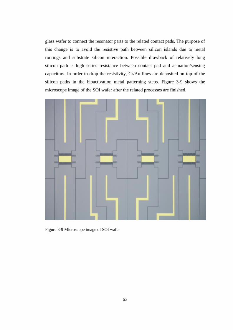
63
glass wafer to connect the resonator parts to the related contact pads. The purpose of
this change is to avoid the resistive path between silicon islands due to metal
routings and substrate silicon interaction. Possible drawback of relatively long
silicon path is high series resistance between contact pad and actuation/sensing
capacitors. In order to drop the resistivity, Cr/Au lines are deposited on top of the
silicon paths in the bioactivation metal patterning steps. Figure 3-9 shows the
microscope image of the SOI wafer after the related processes are finished.
Figure 3-9 Microscope image of SOI wafer

64
SEM images of each resonator after SOI process are presented in Figure 3-10.
Figure 3-10 SEM images of each resonator type
Another difference from the previous generation process flow is the locations of the
contact pads. As seen from the SEM images of the SOI on Figure 3-11, drive and
sense ports are placed across the die to reduce the feedthrough capacitance.
Experimental results show that feedthrough current drops to about 500 aF (1/100 of
the previous generation resonators).
c)a)
RCGS#1
b)
RCGS#2 RCGS#3
d)
RCGS#4
e)
RCGS#5

65
Figure 3-11 Scanning electron microscope (SEM) view of a resonator after structural DRIE
step
During the glass process, two different etch for recess gaps and microchannel is no
more necessary since there are no metal wirings inside the recesses. Only the wire
bond pad and the related routing lines are patterned inside the recess gaps.
Therefore, single pure HF wet glass etch is enough. Metal patterning is done to
create a mask for the HF etch. After the glass etch, the metal mask is stripped and
the sharp trenches created by the aggressive pure HF etch is smoothened in BHF.
PR
OF
MA
SS
SENSE
DRIVE
CFeed
thro
ugh

66
Then, the glass wafer is coated with Cr/Au (30nm/300nm). As in the previous
generation fabrication flow, wet etch of metal layers are done after photolithography
to form contact pads. An image of the glass wafer after related processes is
presented in Figure 3-12.
Figure 3-12 Microscope image of glass wafer after process completed
Remaining parts are the same with the previous fabrication flow (Anodic bonding,
handle layer removal and parylene coating).
3.3 Fabrication Summary
Used fabrication process flows during the fabrication of resonators have been given
in this chapter. Previously proposed flow investigated and related problems and
possible solutions have been analyzed. In the light of these analyses, an updated
process flow is used to fabricate designed resonator. After fabrication, wafers diced
into single dies and input/output ports were mounted to let liquid inside the
microchannels. Figure 3-14 shows the final form of a die.
Microchannel & resonator cavity
Cavity for
routing lines

67
Figure 3-13 Photograph of resonant mass sensor device integrated with microfluidic channel
cap and fluidic connections.
Next chapter presents the experimental data of the fabricated sensors along with
experimental setup.
Inlet and outlet of
microchannel
Top view Bottom view
Microchannel

68

69
CHAPTER 4
4 EXPERIMENTAL RESULTS
This chapter provides information about the experimental work on the fabricated
sensors. First, designed interface circuit is presented. Then the experimental setup is
shown. Next, the resonance characterization results of the devices in air are given.
After that feedthrough elimination results are emphasized. Finally, chapter is
concluded with mass sensing result of a microbead.
4.1 Interface Electronics
Interface electronics have been designed for the characterization of sensors.
Implementation of electronics was done on printed circuit board (PCB). Designed
board gives the opportunity of working both open and closed loop. Moreover, it
includes feedthrough elimination electronics for different types of sensors. Let’s
look into parts of the read-out electronics in detail.
The first part of the interface electronics is the transimpedance amplifier (TIA). The
purpose of the TIA is to convert the output current of the resonator to electrical
potential. Beside the current to voltage conversion, it also forces output node of the
resonator to the ground potential and eliminates the parasitic capacitive effects.
Figure 4-1 shows the basic design for TIA.

70
Figure 4-1 Transimpedance amplifier architecture
It is important to select an OPAMP with low input current noise since the injected
current from the resonators is at the order of nanoamperes. In order to decrease the
current noise, feedback resistance should also be selected as big as possible since the
noise current is inversely proportional. These two conditions force us to select an
OPAMP with low current noise and high gain-bandwidth product. OPA 656 of
Texas Instruments satisfies both conditions. Current noise performance is around
200 fg/√𝐻𝑧 and gain-bandwidth product is close to 1 GHz.
TIA is sufficient for the open loop measurement of resonator. However, for a proper
closed loop oscillation more parts are necessary. Barkhausen criteria say that closed
loop transfer function should have magnitude of 1 and phase of 0 at oscillation
frequency. In order to achieve these two criteria, a voltage comparator and a phase
shifter is used. Using voltage comparator as a last stage sustains gain of 1 and phase
shifter manipulates the phase response of the system. As previously described an
ideal resonator changes phase response from +90 to -90 and at resonance frequency
phase response of the resonator is exactly 0. However, feedthrough current prevents
the phase change of 180°. Therefore, phase response of the system is no more 0 at
resonance frequency. At this point, phase shifter is used to change the phase
response of the system to ensure phase of 0 at resonance frequency. Figure 4-2
shows the used phase shifter topology. Changing potentiometer value changes the
phase response of the system.

71
Figure 4-2 Phase shifter topology
In this thesis, two different feedthrough elimination methods are suggested and
tested. For the resonators that have single sense port applying two opposite phased
signal is chosen as feedthrough current elimination method. Therefore creating two
signals that have opposite phases is necessary. To have exactly inverted signals,
instrumentational amplifiers are chosen since they have high common mode
rejection ratio (CMRR). Figure 4-3 shows the topology that implemented on PCB.
Rpot

72
Figure 4-3 Electronics that presents two out-of-phased output by utilizing instrumentation
amplifiers
In order to eliminate the feedthrough current of the resonators that have two
differential sense ports electronics for voltage subtraction is necessary. Topology in
Figure 4.4 is used to subtract the output voltage that obtained from two different
sense ports. By changing R1, subtraction ratios of the V1 and V2 can be changed. So
that mismatches of feedthrough capacitance between two sense ports and drive ports
can be overcome.

73
Figure 4-4 Voltage subtractor electronic that is used to eliminate the feedthrough current
An image of the read-out PCB and device under test can be seen in Figure 4-5.
Figure 4-5 A closer look of designed electronics with device under test
Device under test
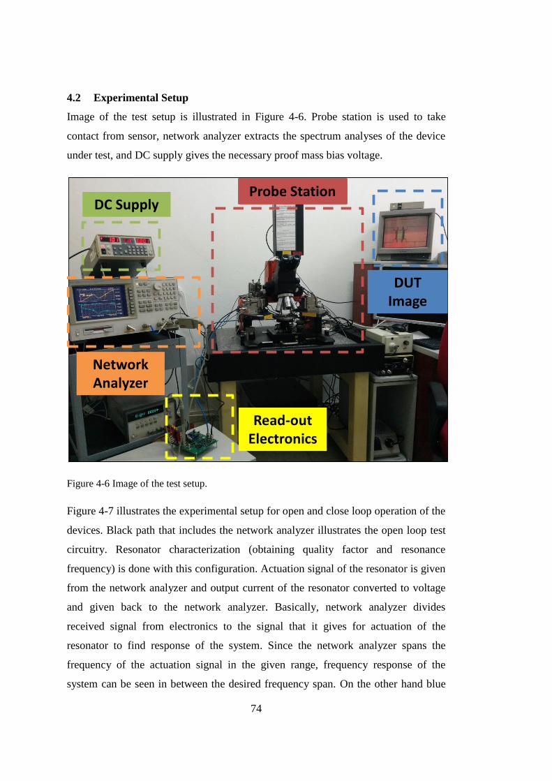
74
4.2 Experimental Setup
Image of the test setup is illustrated in Figure 4-6. Probe station is used to take
contact from sensor, network analyzer extracts the spectrum analyses of the device
under test, and DC supply gives the necessary proof mass bias voltage.
Figure 4-6 Image of the test setup.
Figure 4-7 illustrates the experimental setup for open and close loop operation of the
devices. Black path that includes the network analyzer illustrates the open loop test
circuitry. Resonator characterization (obtaining quality factor and resonance
frequency) is done with this configuration. Actuation signal of the resonator is given
from the network analyzer and output current of the resonator converted to voltage
and given back to the network analyzer. Basically, network analyzer divides
received signal from electronics to the signal that it gives for actuation of the
resonator to find response of the system. Since the network analyzer spans the
frequency of the actuation signal in the given range, frequency response of the
system can be seen in between the desired frequency span. On the other hand blue
Probe Station
DUT Image
Read-out Electronics
DC Supply
Network Analyzer

75
path illustrates the closed loop circuitry. There is an additional phase shifter, which
manually helps system to lock-in resonance frequency. Oscilloscope is used to
observe the waveform of the self-oscillation.
Figure 4-7 Illustration of the experimental setup for open (black line) and close loop (blue
line) operation of devices.
4.3 Resonator Characterization
AC responses of all resonators have been measured in air. For each sensor two
figures are presented. The first one is direct output of the network analyzer that
shows the magnitude and phase response of the overall system. Therefore, this result
includes the feedthrough effect. The second figure is the post-processed data with
the aim of getting response of the only displacement related output current. To do so
results were gathered from the network analyzer in the polar form for both when the
sensor is active (DC bias applied) and passive (DC bias not applied). Data that
contain only the capacitive feedthrough signal (output signal when DC voltage is not
applied on the proof mass) is subtracted from the overall system response (output
signal when DC voltage is applied on the proof mass) in vector domain. Basically
subtraction of the feedthrough output from the total output is done.
4.3.1 RGCS#1
Figure 4-8 is taken from the network analyzer and it shows the open loop magnitude
and phase response of the system with RGCS#1 and TIA. Resonance frequency is
around 204.5 kHz. Note that it is impossible to find the quality factor since 3dB drop
TIA
Proof Mass
VD
C
Voltage Amplifier
Network Analyzer
PhaseShifter
Oscilloscope
Isense
Sense
Act
uat
e
Proof Mass
Closed loop path
Closed loop path
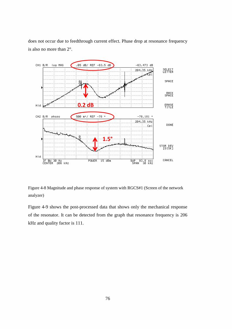
76
does not occur due to feedthrough current effect. Phase drop at resonance frequency
is also no more than 2°.
Figure 4-8 Magnitude and phase response of system with RGCS#1 (Screen of the network
analyzer)
Figure 4-9 shows the post-processed data that shows only the mechanical response
of the resonator. It can be detected from the graph that resonance frequency is 206
kHz and quality factor is 111.
0.2 dB
1.5°

77
Figure 4-9 Magnitude and phase response of RGCS#1 (post-processed data)
4.3.2 RGCS#2
Figure 4-10 illustrates the magnitude and phase response of the system that consists
of RGCS#2 and TIA. Resonance frequency is 226.4 kHz. Quality factor
improvisation can also be extracted from the sharpness of the peak, although post-
processing is necessary for the exact result. Phase drop of almost 15° simply shows
the higher resonator gain against to feedthrough gain compared to RGCS#1.
-150
-100
-50
0
50
100
150
-104
-103
-102
-101
-100
-99
-98
-97
-96
-95
-94
202.0 203.0 204.0 205.0 206.0 207.0 208.0 209.0
Ph
ase
(d
egr
ee
)
Mag
nit
ud
e (
dB
)
Frequency (kHz)
Magnitude and Phase Response of RGCS#1
Magnitude
Phase

78
Figure 4-10 Magnitude and phase response of system with RGCS#2 (Screen of the network
analyzer)
Post-processed data in Figure 4-11 can be used to calculate quality factor. Quality
factor of the resonator is found as 1131.8.
1 dB
12°

79
Figure 4-11 Magnitude and phase response of RGCS#2 (post-processed data)
4.3.3 RGCS#3
Figure 4-11 shows the frequency response of the related sensor and TIA system.
Resonance frequency is 199 kHz, magnitude peak at resonance is around 8 dB and
phase change is around 80°. That means even there is no feedthrough current
elimination, feedthrough effect decreases seriously while comparing previous
sensors.
-100
-80
-60
-40
-20
0
20
40
60
80
100
-115
-110
-105
-100
-95
-90
225.0 225.5 226.0 226.5 227.0 227.5 228.0
Ph
ase
(d
egr
ee
)
Mag
nit
ud
e (
dB
)
Frequency (kHz)
Magnitude and Phase Response of RGCS#2
Magnitude
Phase

80
Figure 4-12 Magnitude and phase response of system with RGCS#3 (Screen of the network
analyzer)
6 dB
60°

81
Figure 4-12 illustrates the post processed data that does not include feedthrough
current. Quality factor is found as 98. Note that it is expected that RGCS#1 and
RGCS#3 have the same resonance frequency and quality factor due to same mass
and spring utilization in both sensors. Test results shows that these two sensors have
close resonance frequency and quality factor values. Minor differences are caused
from fabrication non-uniformities (i.e. Au thickness). One more important point is
the peak gain of the sensor. RGCS#3 has gain of -38 dB whereas it is around -90 dB
for the previous two sensors.
Figure 4-13 Magnitude and phase response of RGCS#3 (post-processed data)
4.3.4 RGCS#4
Purpose of the RGCS#4 is to eliminate feedthrough current by taking difference of
opposite-phased output signals. Figure 4-14 shows that effect of feedthrough current
on system response is very small comparing previous designs. Phase shift around
resonance frequency is more than 100°.
-150
-100
-50
0
50
100
150
-70
-65
-60
-55
-50
-45
-40
-35
160.0 180.0 200.0 220.0 240.0
Ph
ase
(d
egr
ee
)
Mag
nit
ud
e (
dB
)
Frequency (kHz)
Magnitude and Phase Response of RGCS#3
Magnitude
Phase

82
Figure 4-14 Magnitude and phase response of system with RGCS#4 (Screen of the network
analyzer)
Figure 4-15 shows the post processed data that exactly eliminates the feedthrough
current. Quality factor of this resonator is found as 414.
22 dB
>120°
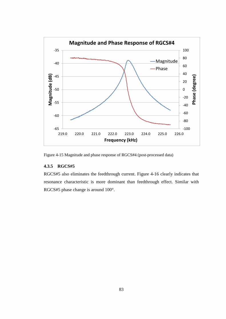
83
Figure 4-15 Magnitude and phase response of RGCS#4 (post-processed data)
4.3.5 RGCS#5
RGCS#5 also eliminates the feedthrough current. Figure 4-16 clearly indicates that
resonance characteristic is more dominant than feedthrough effect. Similar with
RGCS#5 phase change is around 100°.
-100
-80
-60
-40
-20
0
20
40
60
80
100
-65
-60
-55
-50
-45
-40
-35
219.0 220.0 221.0 222.0 223.0 224.0 225.0 226.0
Ph
ase
(d
egr
ee
)
Mag
nit
ud
e (
dB
)
Frequency (kHz)
Magnitude and Phase Response of RGCS#4
Magnitude
Phase
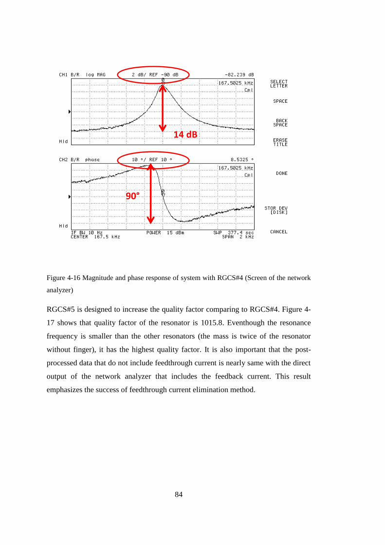
84
Figure 4-16 Magnitude and phase response of system with RGCS#4 (Screen of the network
analyzer)
RGCS#5 is designed to increase the quality factor comparing to RGCS#4. Figure 4-
17 shows that quality factor of the resonator is 1015.8. Eventhough the resonance
frequency is smaller than the other resonators (the mass is twice of the resonator
without finger), it has the highest quality factor. It is also important that the post-
processed data that do not include feedthrough current is nearly same with the direct
output of the network analyzer that includes the feedback current. This result
emphasizes the success of feedthrough current elimination method.
14 dB
90°

85
Figure 4-17 Magnitude and phase response of RGCS#4 (post-processed data)
Summary of resonance characterization is presented in the Table 4.1. Maximum
gain data is the gain between the input voltage of the resonator and the output
voltage of the TIA. Since the resistance of the TIA is 1 MΩ, gain of the resonator
(between input voltage and output current) can be found by dividing the given gain
to 106. However for the RCGS#4 and RCGS#5 voltage subtractor which is
established for the feedthrough current elimination adds additional gain. Since the
gain of the voltage subtractor is feedthrough current mismatch dependent, maximum
gain data for these two sensors is not meaningful for comparison.
-80
-60
-40
-20
0
20
40
60
80
100
-96
-94
-92
-90
-88
-86
-84
-82
167.2 167.3 167.4 167.5 167.6 167.7 167.8
Ph
ase
(d
egr
ee
)
Mag
nit
ud
e (
dB
)
Frequency (kHz)
Magnitude and Phase Response of RGCS#4
Magnitude
Phase

86
Table 4-1 Important measured parameters of different resonator designs.
Sensor Resonance
Frequency
Quality
Factor
Max.
Gain
Sense
Type
RCGS#1
206 kHz 111 -95 dB Single
RCGS#2
226.4 kHz 1132 -92 dB Single
RCGS#3
199 kHz 98 -38 dB Single
RCGS#4
223 kHz 414 NM Differential
RCGS#5
167.5 kHz 1016 NM Differential

87
4.4 Results of feedthrough elimination with dummy signal
For the feedthrough elimination two different methods were investigated in the
theory chapter. Success of the differential sense method is already emphasized in the
previous section.
The other method that uses two opposite-phased drive signals (one is not for
actuation) was tested on previously fabricated sensors [33]. Figure 4.18 shows the
tested sensor and related results. There is a dramatic decrease in feedthrough effect
when the two feedthrough signals are exactly opposite phased. Effect of phase
mismatch, which is theoretically calculated, can be seen from the results (Figure 4-
18 c-d). However, it should be noted that, capacitive mismatches in the resonator
may raise a problem in achieving exactly opposite phased signals, and hence the
feedthrough current may not be perfectly eliminated.
Drive of res. 1
Drive of res. 2
Sen
se
(Co
mm
on
)
100 µm
a) 0.2 dB
25°
Feed
thro
ugh
gai
n
3.2
dB
b)
Fee
dth
rou
gh g
ain
-1
5 d
B
120 °
0.2 dB
c)
Fee
dth
rou
gh g
ain
-2
2 d
B 17 dB
170 °
d)

88
Figure 4-18 AC response of the gravimetric cell sensor (a) under different test
conditions is given. In part b) the resonator is driven using single drive electrode and
very small resonance peak is observed. In part c) the resonator is driven using
differential driving method but phases of drive signals are roughly out-of-phase.
Feedthrough current decreased 15 dB and 7dB resonance peak is observed. In part d)
phases of drive signals are enforced to be exactly 180° and feedthrough current is
decreased 7dB compared to that in part c.
4.5 Mass sensing
In order to test the mass sensitivity, 10 µm (±10%) diameter latex beads of Sigma-
Aldrich® were selected as load. The mass density of these beads is very close to the
density of water. Mass of a bead is calculated as 550 fg. Figure 4-19 shows the bead
placed on the sensor. An RCGS#4 resonator is used for these tests.
Figure 4-19 Microbead loaded sensor.
Loaded and unloaded resonance frequencies of the sensor were measured. Square of
the ratios of these frequencies gives the mass ratios of loaded and unloaded sensor.
Figure 4-20 shows the frequency responses of loaded and unloaded sensor.
Resonance frequency of the unloaded sensor is 207.34 kHz and the loaded sensor is
207.28 kHz. Mass of the unloaded sensor is calculated as 909 ng including Si, Cr/Au
and parylene. In the light of these data, mass change due to the added micro bead is
experimentally found as 0.526 ng, corresponding to 60 Hz resonance frequency
shift.
Microbead

89
Figure 4-20 Resonant spectrum of loaded and unloaded cases
4.6 In-liquid resonant characterization
It has been already reported that parylene coated lateral resonant structures remains
functional in-liquid despite a quality factor drop [22], [32]. Verification of this claim
has been done by RCGS#2. Resonant spectra of the sensor were extracted for dry
and wet cases. Figure 4-21 & 4-22 show the resonant spectrum comparisons of
magnitude and phase, respectively. Quality factors and resonance frequencies are
found as 402 and 219.7 kHz for the dry case, and 183 and 219.6 kHz for the wet
case.
-83
-82
-81
-80
-79
-78
-77
-76
-75
-74
-73
206.0 206.5 207.0 207.5 208.0 208.5 209.0
Mag
nit
ud
e (
dB
)
Frequency (kHz)
Resonant spectrum of loaded and unloaded cases
Unloaded
Loaded
60 Hz

90
Figure 4-21 Resonant spectrum of wet and dry sensors (magnitude comparison)
Figure 4-22 Resonant spectrum of wet and dry sensors (phase comparison)
This result concludes the experimental section. Next section concludes the thesis and
gives the suggestions of future works.
-120
-115
-110
-105
-100
-95
-90
217.5 218.0 218.5 219.0 219.5 220.0 220.5 221.0 221.5
Mag
nit
ud
e (
dB
)
Frequency (kHz)
Resonant spectrum of wet and dry sensors
wet dry
-100
-80
-60
-40
-20
0
20
40
60
80
100
217.5 218.0 218.5 219.0 219.5 220.0 220.5 221.0 221.5
Ph
ase
(°)
Frequency (kHz)
Resonant spectrum of wet and dry sensors
wet dry

91
CHAPTER 5
5 CONCLUSIONS AND FUTURE WORK
The main objective of this thesis is to enable real-time mass measurement for cell
detection applications. Analysis of the benchmark design, which is previously
developed in METU BioMEMS research group, is done to emphasize the inefficient
comb finger structure that prevents the real-time detection. In the light of these
analyses four new sensors are implemented. Proposed sensors did not only improved
the quality factor and sensor gain but also eliminated the feedthrough current effect
to ensure self-oscillation. RCGS#3 showed that optimizing the sensor gain enables a
safe margin for self-oscillation of the resonator. On the other hand, RCGS#5 has less
gain but thanks to high quality factor and differential sense ports it is able to detect
smaller masses.
Summary of the achieved objectives throughout this study can be listed as follows:
The theory behind the operation of mechanical resonant structures is studied
by using the second order spring, mass and damper systems. Electrostatic
capacitive actuation and sensing mechanisms are analyzed and used method
in the designs is verified. Feedthrough effect is introduced and two different
solutions are proposed.
Design considerations, including fabrication limitations and application
trade-offs are discussed. New device designs are presented. Mathematical
analysis of each design is shown and important gain equations of different
designs are calculated and drawn on MATLAB for the purpose of
comparison.
Previously proposed fabrication process flow is investigated. Fabrication
related problems have been detected and proper solutions have been

92
proposed. In the light of this analysis, a new process flow is proposed.
Device fabrication including SOI, glass and polymer micromachining has
been successfully completed.
A discrete interface circuit, which is implemented with high performance
off-the-shelf components on a PCB, is used for resonant characterization of
the sensors, realization of feedthrough elimination methods, and closed-loop
self-oscillation.
Resonance characterization experiments in air have been performed. Two
order of magnitude gain increase and 10 times quality factor increase have
been achieved without increasing the sensor mass.
Feedthrough current elimination with two methods has been accomplished.
Mass detection experiments have been done with fabricated sensors.
Polystyrene microbeads have been used as mass load. Mass of micro bead is
experimentally found as 0.526 ng, corresponding to 60 Hz resonance
frequency shift.
Resonance characterization of sensor in water has been done to verify the
effect of parylene layer. The quality factor of measured sensor decreased
only to 183 in water, form 402 in air.
Real time cell detection in liquid environment is enabled in the light of the
reported improvements.
Future work on this topic can be summarized as:
Parylene coating of the wafers were done after the anodic bonding due to
high bonding temperature. Therefore, parylene patterning and selective etch
could not be done. As a solution, parylene bonding can be used instead of
anodic bonding. Both SOI and glass wafers can be parylene coated and
parylene can be etched selectively with RIE. Although bonding quality
decreases comparing to anodic bonding, this method brings the opportunity
of parylene patterning [35].
In-liquid real-time cell detection tests can be conducted.
Bioactivation for different analytes can be performed to widen the
application areas.

93
Device can be integrated with the cell separation purposed MEMS devices to
increase the detection success.

94

95
REFERENCES
[1] Y. Demircan, “Detection of Imatinib and Doxorubicin Resistance in K562
Leukemia Cells by 3D-Electrode Contactless Dielectrophoresis,” Middle East
Technical University, 2013.
[2] R. Bashir, “BioMEMS: State-of-the-art in detection, opportunities and
prospects,” Adv. Drug Deliv. Rev., vol. 56, no. 11, pp. 1565–1586, 2004.
[3] R. Bashir, An Introduction to BioMEMS and Bionanotechnology. 2005.
[4] K. Menon, R. A. Joy, N. Sood, and R. K. Mittal, “The Applications of
BioMEMS in Diagnosis, Cell Biology, and Therapy: A Review,”
Bionanoscience, vol. 3, no. 4, pp. 356–366, 2013.
[5] W.-T. Liu, L. Zhu, Q.-W. Qin, Q. Zhang, H. Feng, and S. Ang, “Microfluidic
device as a new platform for immunofluorescent detection of viruses.,” Lab
Chip, vol. 5, no. 11, pp. 1327–1330, 2005.
[6] J. H. Wang, C. H. Wang, W. S. Ling, L. Jheng, S. W. Wang, and G. Bin Lee,
“Integrated microfluidic system for HIV detection,” Proc. IEEE Int. Conf.
Micro Electro Mech. Syst., vol. 1, no. February, pp. 961–964, 2012.
[7] C. W. Huang, H. T. Hsueh, Y. J. Huang, H. H. Liao, H. H. Tsai, Y. Z. Juang,
T. H. Lin, S. S. Lu, and C. T. Lin, “A fully integrated wireless CMOS
microcantilever lab chip for detection of DNA from Hepatitis B virus
(HBV),” Sensors Actuators, B Chem., vol. 181, pp. 867–873, 2013.
[8] J. Chen, J. Li, and Y. Sun, “Microfluidic approaches for cancer cell detection,
characterization, and separation,” Lab Chip, vol. 12, no. 10, p. 1753, 2012.
[9] K. Takahashi, R. Ozawa, H. Oyama, M. Futagawa, F. Dasai, M. Ishida, and
K. Sawada, “A CMOS-MEMS-based label-free protein sensor for high-
sensitive and compact system,” Tech. Dig. - Int. Electron Devices Meet.
IEDM, pp. 553–556, 2012.
[10] Z. Mei, S. H. Cho, A. Zhang, J. Dai, T. F. Wu, and Y. H. Lo, “Counting
leukocytes from whole blood using a lab-on-a-chip coulter counter,” Proc.
Annu. Int. Conf. IEEE Eng. Med. Biol. Soc. EMBS, pp. 6277–6280, 2012.
[11] S. Bhattacharya, J. Jang, L. Yang, D. Akin, and R. Bashir, Rapid Detection of
Biological Entities, vol. 15. 2007.

96
[12] U. E. Keller, Chemical Sensors and Biosensors for Medical and Biological
Applications. 1998.
[13] J. Liu and B. Mattiasson, “Microbial BOD sensors for wastewater analysis,”
Water Res., vol. 36, no. 15, pp. 3786–3802, 2002.
[14] M. J. Heller, a H. Forster, and E. Tu, “Active microeletronic chip devices
which utilize controlled electrophoretic fields for multiplex DNA
hybridization and other genomic applications.,” Electrophoresis, vol. 21, no.
1, pp. 157–164, 2000.
[15] R. Bhatia, J. W. Dilleen, a. L. Atkinson, and D. M. Rawson, “Combined
physico-chemical and biological sensing in environmental monitoring,”
Biosens. Bioelectron., vol. 18, no. 5–6, pp. 667–674, 2003.
[16] Ö. S. LAÇIN, “A High Throughput Parylene Microchannel Coulter Counter
For Cell Sizing And Cell Counting Applications,” Middle East Technical
University, 2014.
[17] N. V. Lavrik, M. J. Sepaniak, and P. G. Datskos, “Cantilever transducers as a
platform for chemical and biological sensors,” Rev. Sci. Instrum., vol. 75, no.
7, pp. 2229–2253, 2004.
[18] H. S. Wasisto, S. Merzsch, A. Waag, E. Uhde, T. Salthammer, and E. Peiner,
“Airborne engineered nanoparticle mass sensor based on a silicon resonant
cantilever,” Sensors Actuators, B Chem., vol. 180, pp. 77–89, 2012.
[19] T. P. Burg, M. Godin, S. M. Knudsen, W. Shen, G. Carlson, J. S. Foster, K.
Babcock, and S. R. Manalis, “Weighing of biomolecules, single cells and
single nanoparticles in fluid.,” Nature, vol. 446, no. 7139, pp. 1066–1069,
2007.
[20] S. Olcum, N. Cermak, S. C. Wasserman, K. S. Christine, H. Atsumi, K. R.
Payer, W. Shen, J. Lee, A. M. Belcher, S. N. Bhatia, and S. R. Manalis,
“Weighing nanoparticles in solution at the attogram scale.,” Proc. Natl. Acad.
Sci. U. S. A., vol. 111, no. 4, pp. 1310–5, 2014.
[21] K. Park, J. Jang, D. Irimia, J. Sturgis, J. Lee, J. P. Robinson, M. Toner, and R.
Bashir, “‘Living cantilever arrays’ for characterization of mass of single live
cells in fluids.,” Lab Chip, vol. 8, no. 7, pp. 1034–1041, 2008.
[22] E. Bayraktar, D. Eroglu, A. T. Ciftlik, and H. Kulah, “A MEMS based
gravimetric resonator for MASS sensing applications,” Proc. IEEE Int. Conf.
Micro Electro Mech. Syst., pp. 817–820, 2011.
[23] D. Eroglu and H. Kulah, “JMEMS Letters in Liquid Media by Hydrophobic
Coating,” vol. 20, no. 5, pp. 1068–1070, 2011.
97
[24] D. Eroglu, E. Bayraktar, and H. Kulah, “A laterally resonating gravimetric
sensor with uniform mass sensitivity and high linearity,” 2011 16th Int. Solid-
State Sensors, Actuators Microsystems Conf. TRANSDUCERS’11, pp. 2255–
2258, 2011.
[25] A. Rahafrooz and S. Pourkamali, “High-frequency thermally actuated
electromechanical resonators with piezoresistive readout,” IEEE Trans.
Electron Devices, vol. 58, no. 4, pp. 1205–1214, 2011.
[26] A. Hajjam, A. Rahafrooz, and S. Pourkamali, “Sub-100ppb/??C temperature
stability in thermally actuated high frequency silicon resonators via
degenerate phosphorous doping and bias current optimization,” Tech. Dig. -
Int. Electron Devices Meet. IEDM, no. 303, pp. 170–173, 2010.
[27] T. Wavering, S. Meller, M. Evans, C. Pennington, M. Jones, R. Van Tassell,
K. Murphy, P. Drive, and E. Valdes, “Interferometric Optical Fiber
Microcantilever Beam Biosensor,” vol. 4200, no. 2000, pp. 10–16, 1872.
[28] B. R. Ilic, S. Krylov, M. Kondratovich, and H. G. Craighead, “Optically
actuated nanoelectromechanical oscillators,” IEEE J. Sel. Top. Quantum
Electron., vol. 13, no. 2, pp. 392–398, 2007.
[29] A. T. Lin, J. E. Lee, J. Yan, and A. A. Seshia, “ENHANCED
TRANSDUCTION METHODS FOR ELECTROSTATICALLY DRIVEN
MEMS RESONATORS A . T-H . Lin , J . E-Y . Lee , J . Yan , A . A . Seshia
Cambridge , UNITED KINGDOM MEASUREMENT THEORY & SETUP,”
pp. 561–564, 2009.
[30] S. E. Alper, “An Analysis To Improve Stability of Drive-Mode Oscillations in
Capacitive Vibratory MEMS Gyroscopes,” in Transducers, 2011, pp. 817–
820.
[31] J. E. Y. Lee and a. a. Seshia, “Parasitic feedthrough cancellation techniques
for enhanced electrical characterization of electrostatic microresonators,”
Sensors Actuators, A Phys., vol. 156, no. 1, pp. 36–42, 2009.
[32] D. Eroglu, “Development of a Resonant Mass Sensor for MEMS Based Cell
Detection Applications,” Middle East Technical University, 2012.
[33] T. B. TÖRAL, “Development of a High Yield Fabricatiom Process for
MEMS Based Resonant Mass Sensors for Cell Detection Applications,”
MIDDLE EAST TECHNICAL UNIVERSITY, 2014.
[34] Y. H. Cho, A. P. Pisano, and R. T. Howe, “Viscous damping model laterally
oscillating microstructures,” J. Microelectromechanical Syst., vol. 3, no. 2,
pp. 81–87, 1994.

98
[35] H. Kim and K. Najafi, “Characterization of low-temperature wafer bonding
using thin-film parylene,” J. Microelectromechanical Syst., vol. 14, no. 6, pp.
1347–1355, 2005.