![TSUBAKI KABELSCHLEPP Parts listkabelschlepp.ru/fileadmin/img/carrier/PDFs/spare... · Item Materialtext [remarks] KR 052 KR 065 KR 095 KR 125 KR 150 KR 180 KR 200 KR 225 1](https://static.fdocuments.in/doc/165x107/5faa70404ba8b17fd45cfabf/tsubaki-kabelschlepp-parts-item-materialtext-remarks-kr-052-kr-065-kr-095-kr-125.jpg)
MEMS Based Deep 1D Photonic Crystal - IntechOpen...MEMS Based Deep 1D Photonic Crystal 85 where rr 2...
34
5 MEMS Based Deep 1D Photonic Crystal Maurine Malak and Tarik Bourouina Université Paris-Est, ESIEE Paris France 1. Introduction Since the Bragg layers, also referred as to 1D photonic crystal, lie at the core of many optical devices, this chapter is devoted to the study of the theory underlying the design of multilayered structures [Macleod 2001]. The corresponding analytical model is explained in details in section 2 followed in the next sections, by various design examples for the shake of illustration. Of special interest are the Silicon-Air Bragg mirrors obtained by DRIE micromachining. They are considered as an important building block leading to a wide variety of applications. First, we elaborate on the use of this building block in resonant cavities and in interferometers (section 3). Then, we apply the multilayered stack theory to a case of study for a special structure: The mode selector, covered in section 3.7). Finally, we conclude this work by highlighting about an advanced architecture of 1D photonic crystals based on curved Bragg mirrors. 2. Theory and modeling of Bragg reflectors Under specific conditions, a stack of multilayered structure gives rise to nearly perfect optical reflectance, approaching 100 %, as compared to the reflectance from a single interface. This is the main characteristic that makes the interest in such structures, called Bragg reflectors or Bragg mirrors. This phenomenon of enhanced reflectivity might be explained by the fact that the presence of two (or more) interfaces means that a number of light beams will be produced by successive reflections, that may interfere constructively (or destructively, when considering anti-reflective surfaces), and the properties of the multilayered film will be determined by the summation of these beams. This might be the case in thin film assemblies. In thick assemblies however, the later phenomenon does not take place. Before going into the analytical details, we differentiate between thin and thick films. We say that the film is thin when interference effects can be detected in the reflected or transmitted light, that is, when the path difference between the beams is less than the coherence length of the light, and thick when the path difference is greater than the coherence length. Note that no interference can be observed when effects of light absorption dominate within the film, even in the case of thin films. The same film can appear thin or thick depending entirely on the illumination conditions. The thick case can be shown to be identical with the thin case integrated over a sufficiently wide wavelength range or a sufficiently large range of angles of incidence. Normally, we will find that the films on the www.intechopen.com
Transcript of MEMS Based Deep 1D Photonic Crystal - IntechOpen...MEMS Based Deep 1D Photonic Crystal 85 where rr 2...

5
MEMS Based Deep 1D Photonic Crystal
Maurine Malak and Tarik Bourouina Université Paris-Est, ESIEE Paris
France
1. Introduction
Since the Bragg layers, also referred as to 1D photonic crystal, lie at the core of many optical devices, this chapter is devoted to the study of the theory underlying the design of multilayered structures [Macleod 2001]. The corresponding analytical model is explained in details in section 2 followed in the next sections, by various design examples for the shake of illustration.
Of special interest are the Silicon-Air Bragg mirrors obtained by DRIE micromachining. They are considered as an important building block leading to a wide variety of applications. First, we elaborate on the use of this building block in resonant cavities and in interferometers (section 3). Then, we apply the multilayered stack theory to a case of study for a special structure: The mode selector, covered in section 3.7). Finally, we conclude this work by highlighting about an advanced architecture of 1D photonic crystals based on curved Bragg mirrors.
2. Theory and modeling of Bragg reflectors
Under specific conditions, a stack of multilayered structure gives rise to nearly perfect optical reflectance, approaching 100 %, as compared to the reflectance from a single interface. This is the main characteristic that makes the interest in such structures, called Bragg reflectors or Bragg mirrors. This phenomenon of enhanced reflectivity might be explained by the fact that the presence of two (or more) interfaces means that a number of light beams will be produced by successive reflections, that may interfere constructively (or destructively, when considering anti-reflective surfaces), and the properties of the multilayered film will be determined by the summation of these beams. This might be the case in thin film assemblies. In thick assemblies however, the later phenomenon does not take place. Before going into the analytical details, we differentiate between thin and thick films. We say that the film is thin when interference effects can be detected in the reflected or transmitted light, that is, when the path difference between the beams is less than the coherence length of the light, and thick when the path difference is greater than the coherence length. Note that no interference can be observed when effects of light absorption dominate within the film, even in the case of thin films. The same film can appear thin or thick depending entirely on the illumination conditions. The thick case can be shown to be identical with the thin case integrated over a sufficiently wide wavelength range or a sufficiently large range of angles of incidence. Normally, we will find that the films on the
www.intechopen.com

Photonic Crystals – Introduction, Applications and Theory
82
substrates can be treated as thin while the substrates supporting the films can be considered thick.
In the upcoming treatment, we show analytically a generalized model applicable for an absorbing thin film assembly. The obtained result applies equally well for non-absorbing films.
Let’s consider the arrangement shown in Fig. 1 where we denote positive-going waves by the symbol + and negative-going waves by the symbol -. Applying the boundary conditions on the electromagnetic field components at interface B (chosen as the origin of z-axis), we have:
Continuity of the tangential components of the electric filed gives (Eb being the tangential component of the resultant electric field):
1 1b b bE E E (1)
Continuity of the tangential components of the magnetic filed gives (Hb being the tangential component of the resultant magnetic field):
1 1 1 1 1 1b b b b bH H H E E (2)
N1
N2
N0
d
Incidence medium
Substrate
Thin Film
Boundary B
z
し0
Fig. 1. Plane wave incident on a thin film
where ┟ represents the medium admittance such that: ┟ =H/E.
The negative sign in (2) comes from the convention used for the field propagation direction such that the right hand rule relating E, H and K (wave vector, along the propagation direction) is always satisfied. In writing equations (1) and (2), we assume that: Common phase factors have been omitted, and the substrate is thick enough such that no field is reflected back from it.
1 1
1/
2b b bE H E (3)
1 1
1/
2b b bE H E (4)
www.intechopen.com

MEMS Based Deep 1D Photonic Crystal
83
1 1 1 1
1
2b b b bH E H E (5)
1 1 1 1
1
2b b b bH E H E (6)
The fields at the other interface A at the same instant and at a point with identical x and y coordinates can be determined by altering the phase factors of the waves to allow for a shift in the z coordinate from 0 to -d. The phase factor of the positive-going wave will be multiplied by exp(i├) while the negative-going phase factor will be multiplied by exp(-i├), where,
11
2cos
N d (7)
N1 is the refractive index in medium 1, ┠1 is the angle between the z-axis and the propagation direction in medium 1 and ┣ is the free space wavelength. The values of E and H at interface A become:
1 1 1
1/
2i i
a b b bE E e H E e (8)
1 1 1
1/
2i i
a b b bE E e H E e (9)
1 1 1
1
2i i
a b b bH H e H E e (10)
1 1 1
1
2i i
a b b bH H e H E e (11)
So that:
1 1
1
1
2 2
sin cos
i i i i
a a a b b
b b
e e e eE E E E H
iE H
(12)
1 1 1
1
2 2
sin cos
i i i i
a a a b b
b b
e e e eH H H E H
E i H
(13)
In the matrix notation, we finally obtain the following formulation:
1
1
cos sin /
sin cos
a b
a b
E Ei
H Hi
(14)
www.intechopen.com

Photonic Crystals – Introduction, Applications and Theory
84
This matrix relates the tangential components of E and H at the incident interface to tangential components of E and H transmitted through the final interface and it is known as the characteristic matrix of the thin film [M].
Now, let us consider an assembly of thin films as shown in Fig. 2
N1
N2
N0
d1
Incidence medium
Substrate
Thin Film
Boundary A
Boundary B
z
d2
N3
Boundary C
Fig. 2. Plane wave incident on an assembly of thin film
By adding another film to the single film shown in Fig. 1, we can write:
2 2 2
2 2 2
cos sin /
sin cos
b c
b c
E Ei
H Hi
(15)
Combining with equation (14) to get the field at interface A, then we can write:
1 1 1 2 2 2
1 1 1 2 2 2
cos sin / cos sin /
sin cos sin cos
a c
a c
E Ei i
H Hi i
(16)
This result can be immediately extended to the general case of an assembly of q layers, when the characteristic matrix is simply the product of the individual matrices taken in the correct order,
1
cos sin /
sin cos
qa mr r r
a mr r rr
E Ei
H Hi
(17)
where Em and Hm are the electric and magnetic fields components in the substrate plane.
Dividing both sides of equation (17) by Hm, we get:
1
/ 1cos sin /
/ sin cos
qa m r r r
a m mr r rr
B E E i
C H E i
(18)
www.intechopen.com

MEMS Based Deep 1D Photonic Crystal
85
where
2
cosr rr r
N d (19)
cosr r rN for s-polarisation (TE) (20)
/ cosr r rN for p-polarisation (TM) (21)
12 3
0 0/ 2.6544 10 S (Free space admittance) (22)
Then, the admittance of the thin film assembly is:
/
/a a m
a a m
H H E CY
E E E B (23)
The amplitude reflection coefficient and the reflectance are then given by:
0
0
Y
Y
(24)
* *
0 0 0 0
0 0 0 0
Y Y B C B CR
Y Y B C B C
(25)
In this part, we look over the case of absorbing layers. Knowing that K is propagation vector:
2 2 2x zK K K (26)
From Snell’s law, 0x xr xmK K K this leads to:
0 0sin sin sinr r m mN N N (27)
In case of absorbing medium, Nr is complex and in general, it can be expressed as a complex number:
rN n ik (28)
Then,
2 2 2 2 2 2 2 2 2 2 2 20 0 0 0 0 0sin 2 sinzr r xr rK K K K N N K n k ink N (29)
Then,
12
12
2 2 2 20 0 0
2 2 2 20 0
2 sin
2 2 sin
r zr r r
r r r r r
K d K d n k ink N
d n k in k N
(30)
www.intechopen.com

Photonic Crystals – Introduction, Applications and Theory
86
Accordingly, we get:
The admittance of layer r in s-polarization:
122 2 2 2
0 02 sinrs r r r rn k in k N (31)
The admittance of layer r in p-polarization:
222r rr
rprs rs
n ik (32)
In this last part of the analytical model, we present closed form relations for the transmittance T and the absorbance A using the definition of irradiance. If we consider the net irradiance at the exit of the assembly Ik:
* * *1 1Re Re
2 2k k k m k kI E H E E (33)
The net irradiance at the entrance of the assembly Ia:
** * * *
*
1 1 1Re Re Re
2 2 2a a
a a a k k k kk k
E HI E H E E BC E E
E E
(34)
Let the incident irradiance be denoted by Ii, then the irradiance actually entering the assembly becomes:
* *11 Re
2a i k kI R I BC E E (35)
Then,
* *Re
2 1
k k
i
BC E EI
R (36)
The transmittance is then given by:
*
Re 1
Re
mk
i
RIT
I BC
(37)
From equation (25), we get:
0
*0 0
4 Re mTB C B C
(38)
Knowing that A + R + T = 1 from the energy conservation rule, then A becomes:
*
Re1 1 1
Re
mA R T RBC
(39)
www.intechopen.com

MEMS Based Deep 1D Photonic Crystal
87
From equation (25), we get:
*
0
*0 0
4 Re mBCA
B C B C
(40)
3. Microfabricated silicon-Air Bragg as basic building blocks in cavities and interferometers
3.1 Literature survey
Many groups worked on the realisation of silicon-Air Bragg reflectors as basic building blocks in Fabry-Perot (FP) cavities as well as in Michelson interferometers. When considering Fabry-Perot cavities, the use of high reflectance Bragg mirrors is intended to achieve high quality factor Q at the corresponding resonant wavelengths. The use of silicon restricts the wavelength range to the infra-red region. In the same time, light coupling using optical fibers is facilitated by the microfabrication of U-grooves for supporting the fibers with pre-alignment capability. Among the groups working on this topic, we can cite [Lipson & Yeatman 2007] from the imperial college who realized FP cavities obtained by KOH etching on SOI substrate. The best reported value of Q was 2395 in static designs while it was limited to 515 in the MEMS designs due to the rotation associating the translation of the MEMS mirror. Thus, the mirrors became unparallel and the Q-factor degraded. Another group is the group of Ecole Polytechnique de Montreal who realized FP cavity for inertial sensing [Zandi et al 2010] on SOI. Their Q was limited to 662. A third group is that of [Yun and Lee 2003] from Gwangju Institute of Science and Technology, Korea who realized thermally tuned FP cavities, they obtained a Q of 1373. A fourth group is that of [Pruessner et al. 2008] from Naval Research Laboratory, Washington D.C. who realised FP cavities with integrated SOI rib waveguides by cryogenic etching. They recorded a Q factor of 27,000. Lastly, our group at ESIEE Paris was among the pioneers in this domain. In our first achievements, we realized FP cavities with different architectures [Saadany et al. 2006]; the best recorded Q was 1291 for FP structure working as a notch filter. More recently, the performance was improved using cylindrical Bragg mirrors of cylindrical shapes combined with a fiber rod lens, leading to Q = 8818 on quite large cavities exceeding L = 250 µm [Malak et al. APL 2011], an unreached value for the figure of merit Q.L, which is of primary importance for cavity enhancement applications. Table 1 summarizes the specifications of the different designs discussed above.
3.2 Fabrication technology for Si-Air Bragg reflectors (for MEMS and for fixed structures)
In this section, the basic steps of the fabrication process for MEMS structures involving
Bragg layers are highlighted. Many techniques can be used to produce vertical structures on
silicon substrate as mentioned in [Lipson & Yeatman 2005], [Yun et al. 2006] and [Song et al
2007]. They are based on either dry or wet etching of silicon using KOH. The process
described here and shown in Fig. 3 pertains to the (optional) integration of MEMS structures
together with the Bragg mirrors using dry etching.
Starting from a raw SOI wafer, we proceed by making thermal oxidation for the whole wafer. In the next step, photoresist (PR) is used to cover the entire wafer where it acts as a
www.intechopen.com

Photonic Crystals – Introduction, Applications and Theory
88
Lispon and Yeatman
Imperial college UK
Zandi et al.Ecole
Polytec. de Montréal Canada
Yun and Lee Gwangju
Institute of Science and Technology
Korea
Pruessner et al.Naval research
lab Washington
D.C
Saadany et al.
ESIEE France
Malak et al.
ESIEE France
Cavity length
3.3 µm 27.1 µm ---- 12 µm 10 µm 250 µm
Tuning range
Static design : 70 nmMEMS design: 10 nm
30 nm 9 nm 6.7 nm ---- ----
Number of silicon
layers per mirror
3 3 2 2 3 4
Q-factor
Static design: Q = 2395
MEMS design: Q = 515
QMEMS < Qstatic Because the
displacement creates a rotation for the moving mirror.
Q = 662
Qaverage = 1373 (estimated from the response of a rejection filter)
Q = 27000 QTrans =
1291 Q = 8818
Table 1. Summary of the specifications for state-of-the-art FP cavities
mask for photolithography. The PR is then patterned using UV exposure over the DRIE layout mask. Since the PR is a positive type, the areas exposed to UV remain soft while the non-exposed areas become hard and they can not be removed in the development step. Now, the hardened PR acts as a protection mask for the originally oxidized silicon which is patterned using either Reactive Ion etching (RIE) or Buffer HydroFluoric acid (BHF). The role of PR ends here and it is completely removed from the wafer.
The fabrication process continues by the metal deposition over the whole wafer. The metal is patterned by photolithography using the frontside metal layout mask and then etched. In the next step, metal is deposited on the backside of the wafer where it is patterned by the backside layout mask and then etched. We turn again to the front side to make Deep Reactive Ion etching (DRIE) for the silicon structure layer [Marty et al. 2005]. At that level, both the oxide and the aluminum serve as mask materials for silicon etching by DRIE. Processing the backside again, DRIE is done for the backside, in this case, only aluminum serve as mask material for silicon etching by DRIE. The process ends by releasing the MEMS structure in which the insulating oxide is removed by vapor HF.
For the fixed structures involving Bragg mirrors presented in this research work, the process differs from the one detailed above. So, in the next paragraph, we highlight the fabrication process as shown in Fig. 4, used for the realization of the fixed structures.
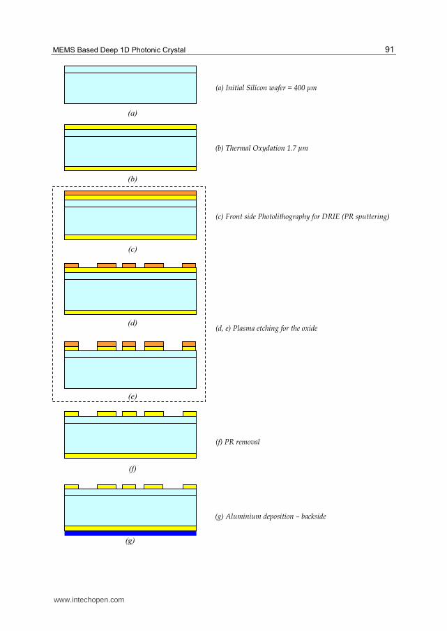
Starting with an ordinary silicon wafer, a thermal oxidation process is carried for both sides of the wafer to achieve an oxide thickness = 1.7 ┤m. Next, PR used as a mask for photolithography, is sputtered over the entire wafer. This step is followed by the photolithography for DRIE mask for the front side and the PR is patterned accordingly. The following step is the plasma etching for the oxide. This photolithography ends by PR
www.intechopen.com

MEMS Based Deep 1D Photonic Crystal
89
removal. Then, we start processing for the back side by depositing aluminium. Next, we pattern the aluminium mask by photolithography using the back side layout mask. Then, we proceed by DRIE etching over 300 ┤m for the back side and the process ends up with DRIE etching for the front side over 100 ┤m. Note that all steps performed on the backside are optional, depending on the nature of the target device.
(b)
(c)
(d)
(e)
(f)
(a)
(e) Oxide etching (using Photoresist patterns as a protection mask material) either by BHF or by RIE
(f) Photoresist removal
(d) Patterning Photoresist by UV exposure and further development
(a) Initial SOI Wafer
(b) Thermal Oxydation
(c) Photoresist spin-coating
www.intechopen.com

Photonic Crystals – Introduction, Applications and Theory
90
(g)
(h)
(i)
(j)
(k)
(l)
(g) Aluminum deposition (sputtering)
(h) Lithography patterning and aluminum etching
(i) Metal deposition on the backside, patterning using proper mask and then, etching.
(j) DRIE Etching for the frontside (Note that here, both oxide and aluminum serve as mask materials for silicon etching by DRIE
(k) DRIE Etching for the backside (Note that in this case, only aluminum serve as mask material for silicon etching by DRIE)
(l) Release (oxide removal by vapor HF)
Fig. 3. (a-l) Basic steps of the fabrication process for MEMS structures co-integrated with Si-Air Bragg mirrors.
www.intechopen.com
MEMS Based Deep 1D Photonic Crystal
91
(a) Initial Silicon wafer = 400 ┤m
(b) Thermal Oxydation 1.7 ┤m
(c) Front side Photolithography for DRIE (PR sputtering)
(d, e) Plasma etching for the oxide
(f) PR removal
(g) Aluminium deposition – backside
(a)
(b)
(c)
(d)
(e)
(f)
(g)
www.intechopen.com

Photonic Crystals – Introduction, Applications and Theory
92
(h)
(i)
(j)
(h) DRIE Photolithography (Oxide + Aluminum)
(i) DRIE Etching – backside 300 um
(j) DRIE Etching – frontside 100 um
Fig. 4. (a-j) Basic steps of the fabrication process for fixed structures involving Bragg mirrors.
3.3 Modeling and simulation of planar Bragg mirror reflectors
Based on the analytical model presented in section 2, then if we have a single layer whose thickness is an odd number of quarter the wavelength, the characteristic matrix of the layer [M] becomes:
0 /
0
iM
i
(41)
So, if we stack a combination of several layers alternatively of High refractive index, denote H, and Low refractive index, denoted L, whose thickness is an odd number of ┣/4 (where ┣ is the wavelength in the corresponding medium), we can construct a high reflectance mirror named Bragg mirror. In the particular case where we stack a combination of five quarter-wave layers which are different, mathematical manipulation of the equivalent characteristic matrix yields an equivalent admittance for the assembly:
2 2 21 3 52 22 4 m
Y (42)
where the definitions presented previously are kept unchanged.
For ┟m=┟0, and considering similar indices for the high and low layers as well so that, ┟1=┟3=┟5=┟H and ┟2=┟4 =┟L , the reflectance of the assembly becomes:
www.intechopen.com
MEMS Based Deep 1D Photonic Crystal
93
26
*
0 06
0 0
1
1
H
L
H
L
Y YR
Y Y
(43)
In general, for a pair (p) of HL layers with similar ┟m and ┟0, we can write:
22
2
1
1
p
H
Lp
H
L
R
(44)
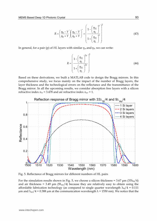
Based on these derivations, we built a MATLAB code to design the Bragg mirrors. In this comprehensive study, we focus mainly on the impact of the number of Bragg layers, the layer thickness and the technological errors on the reflectance and the transmittance of the Bragg mirror. In all the upcoming results, we consider absorption free layers with a silicon refractive index nSi = 3.478 and air refractive index nair = 1.
1500 1510 1520 1530 1540 1550 1560 1570 1580 1590 16000
0.2
0.4
0.6
0.8
1Reflection response of Bragg mirror with 33
Si/4 and 9
Air/4
Wavelength (nm)
Re
fle
cta
nce
1 Si layer
2 Si layers
3 Si layers
4 Si layers
Fig. 5. Reflectance of Bragg mirrors for different numbers of HL pairs
For the simulation results shown in Fig. 5, we choose a silicon thickness = 3.67 ┤m (33┣Si/4) and air thickness = 3.49 ┤m (9┣air/4) because they are relatively easy to obtain using the affordable fabrication technology (as compared to single quarter wavelength ┣Si/4 = 0.111 µm and ┣air/4 = 0.388 µm at the communication wavelength ┣ = 1550 nm). We notice that the
www.intechopen.com

Photonic Crystals – Introduction, Applications and Theory
94
reflectance in the mid-band increases as the number of layers increases which goes in accordance with relation (44). In fact, the reflectance increases from 71.8 % (single Si layer) up to 99.98 % (4 Si layers) when the number of HL pairs increases from single to four. Also, the mirror response becomes sharper and its bandwidth (BW) decreases as the number of layers increases. In the case of single layer, the BW is about 65 nm and it goes down to 58 nm as the HL pairs increases to 4.
In the next simulation, we study the impact of the silicon layers thickness on the mirror bandwidth. For this shake, we consider 4 HL pairs with fixed air layers thickness 3.49 ┤m (9┣air/4), while the thickness of the silicon layers is increased from ┣Si/4 up to 25┣Si/4 in steps of 2┣Si. Simulation results, depicted in Fig 6, show that the mirror BW decreases as the thickness of the silicon layers increases. For silicon thickness ┣Si/4, the 3dB-BW = 238 nm and it decreases to 73 nm at a thickness of 25┣Si/4.
1450 1500 1550 1600 1650 17000
0.1
0.2
0.3
0.4
0.5
0.6
0.7
0.8
0.9
1
Reflection response of Bragg mirror for various silicon thicknesses
Wavelength (nm)
Re
fle
cta
nce
si
/4
9si
/4
17si
/4
25si
/4
Fig. 6. Reflectance of 4 HL pairs for various H thicknesses, L thickness is fixed to 9┣air/4
If on the other hand, we fix the thickness of the silicon layers to 33┣Si/4, for the same 4 HL pairs, and increase the thickness of the air layers from ┣air/4 up to 13┣air/4 in steps of ┣air. A similar effect is noticed but on a smaller BW scale since the BW decreases from 65 nm at L thickness = ┣air/4, to 55 nm at L thickness = 13┣air/4. The corresponding results are shown in Fig. 7. Comparing between both results, we can say that the decrease in the H thickness is more pronounced than the decrease in the L thickness in terms of the bandwidth. Good control of the H thickness can give rise to Bragg mirrors with large BW.
Another point of interest for the Bragg mirror is the technological error. The critical dimension, defined as the minimum feature size on the technology mask, can not be maintained as drawn in the original design and thus, it translates into reduced layer thicknesses on the fabricated device. In fact, the thickness of the silicon layer may vary
www.intechopen.com

MEMS Based Deep 1D Photonic Crystal
95
1500 1510 1520 1530 1540 1550 1560 1570 1580 1590 16000
0.2
0.4
0.6
0.8
1Reflection response of Bragg mirror for various air layer thicknesses
Wavelength (nm)
Re
fle
cta
nce
air
/4
5air
/4
9air
/4
13air
/4
Fig. 7. Reflectance of 4 HL pairs for various L thicknesses, H thickness is fixed to 33┣Si/4
1500 1510 1520 1530 1540 1550 1560 1570 1580 1590 16000
0.1
0.2
0.3
0.4
0.5
0.6
0.7
0.8
0.9
1
X: 1550
Y: 0.005614
Wavelength (nm)
Re
fle
cta
nce
Reflection response of Bragg mirror with introduced errors
error = 100 nm
error = 50 nm
error = 0
error = -50 nm
error = -100 nm
Fig. 8. Reflectance of 4 HL pairs for L thicknesses = 9┣air/4 , H thickness = 33┣Si/4 and several introduced errors.
www.intechopen.com

Photonic Crystals – Introduction, Applications and Theory
96
(increase or decrease) and the air layer follows the opposite trend (decreases or increases). Then, the device performance degrades. This issue is obvious in Fig. 8 where various error values are introduced into the mirror original design. We notice that the overall response shifts toward the left side as the error decreases from 100 nm to -100 nm in steps of 50 nm. Comparing the obtained responses to the error free design, we see that the mirror reflectance might turn from 99.98 % ideally to 0.6 % for an introduced error = ± 100 nm which means that the multilayered designs are not tolerant to fabrication errors exceeding 50 nm.
3.4 Modeling and simulation FP cavity based on Bragg mirrors
If instead of the stack of high reflectance mirror, we introduce a gap layer whose thickness is an integer number of half the wavelength then the characteristic matrix [M] of this layer becomes:
1 0
0 1M
(45)
Thus, we can easily get a Fabry-Perot (FP) resonator if we combine two stacks of quarter wavelengths thick acting as high reflectance mirrors separated by a gap layer of half wavelength thick.
In the next part, we illustrate, by the help of MATLAB simulations, the properties of such FP resonators where we study the impact of several parameters on the resonator spectral response. Parameters of particular interest for this comprehensive study: the mirror reflectance controlled by the number of Bragg layers per mirror, the impact of technological errors and the cavity gap length. In what follows, unless otherwise stated, we consider that the silicon Bragg layers of thickness = 3.67 ┤m (33┣Si/4), the air Bragg layer has a thickness of 3.49 ┤m (9┣air/4) and the gap layer has a width = 10.075 ┤m (13┣Si/2). The silicon refractive index nSi is taken = 3.478 and all the layers are considered absorption free.
We start our study by increasing gradually the number of Bragg layers. As shown in Fig. 9 , we found that the FWHM of the resonator decreases from 7.6 nm for single Si layer/mirror, to 0.56 nm for double Si layer/mirror, to 0.046 nm for 3 Si layers/mirror and finally the FWHM becomes 0.004 nm for 4 Si layers/mirror. This is due to the increase in the mirror reflectance which goes from 71.8 % for single layer to 99.98 % for 4 Si layers. Also, the contrast improves and the minimum level goes from -10 dB up to -70 dB and the resonator sharpness improves as well.
Now, if we consider the case of 4 Si layers/mirror with introduced errors (ε) therein, we obtain the curves shown in Fig. 10 .We notice that the central wavelength ┣0 shifts from 1550 nm by ±8.5 nm as ε = ± 50 nm. For ε = ± 100 nm, ┣0 shifts by 18.15 nm. In addition, the FWHM of the peak increases from 0.004 nm for the error free case to 0.007 nm for ε = ± 50 nm and it reaches 0.029 nm for ε = ±100 nm. This might be explained by reference to previous simulations carried on Bragg mirrors with introduced errors. As mentioned earlier, the overall response of the mirror shifts right (left) as error increases (decreases) and this is the reason underlying the shift in the resonance wavelength. In addition, the maximum reflectance of the mirror decreases from 99.98 % (in the error free case) to 99.97 % (for ±50 nm error) to 99.93 % (for ±100 nm), that’s why the FWHM increases.
www.intechopen.com

MEMS Based Deep 1D Photonic Crystal
97
1500 1510 1520 1530 1540 1550 1560 1570 1580 1590 1600-70
-60
-50
-40
-30
-20
-10
0Transmission of FP resonator based on multilayered Bragg mirrors
Wavelength (nm)
Tra
nsm
issio
n (
dB
)
4 Si layers
3 Si layers
2 Si layers
1 Si layer
Fig. 9. Transmission of FP resonator for different number of silicon layers per mirror.
1530 1535 1540 1545 1550 1555 1560 1565 1570
-70
-60
-50
-40
-30
-20
-10
0Transmission of FP resonator based on multilayered Bragg mirrors with introduced errors
Wavelength (nm)
Tra
nsm
issio
n (
dB
)
= 100 nm
= 50 nm
= 0
= - 50 nm
= -100 nm
Fig. 10. Transmission of FP resonator for different errors.
By scanning over the wavelength for the cases of ε = -50 nm and ε = -100 nm, we notice that other resonance peaks, with larger FWHM and reduced contrast, appear in the spectral response of the cavity. This result seems strange and it does not go in accordance with the designed FSR for the error free cavity. In fact, the designed cavity gap length = 10.075 ┤m corresponding to a quasi FSR = 119.2 nm and a resonance wavelength = 1550 nm.
www.intechopen.com

Photonic Crystals – Introduction, Applications and Theory
98
This issue might be explained by looking over the reflection response of the Bragg mirrors with introduced errors as shown in Fig. 11, we find that they are shifted as compared to the error free design. Moreover, they exhibit a non-negligible reflectance between 1575 nm and 1600 nm and so the design performs as a good resonator.
Analyzing the simulation results, we come out with a new definition for the cavity length named: The effective length Leff. This new parameter suggests that the effective reflecting interfaces of the resonator lie inside the Bragg reflectors and not between the inner interfaces as conventionally thought and so it gives rise to unexpected resonances within the quasi FSR. Making inverse calculations for the simulation results shown in Fig. 12, we find that for ε = -50 nm, the FSR = 52.15 nm corresponding to Leff = 23 ┤m and for ε = -100 nm, the FSR = 47.7 nm corresponding to Leff = 25.18 ┤m.
1500 1510 1520 1530 1540 1550 1560 1570 1580 1590 16000
0.2
0.4
0.6
0.8
1
Reflection response of Bragg mirror with introduced errors
Wavelength (nm)
Reflecta
nce
= -50 nm
= -100 nm
Fig. 11. Reflection response of Bragg mirrors for errors = -50 nm and -100 nm.
3.5 Multilayered Si-Air structures for anti-reflection purposes
Antireflection surfaces (usually obtained through additional material coatings) can be obtained also from silicon micromachinned Bragg structures. They can range from a simple single layer having virtually zero reflectance at just one wavelength, to a multilayer system of more than a dozen of layers, having ideally zero reflectance over a range of several decades. The type used in any particular application will depend on a variety of factors, including the substrate material, the wavelength region, the required performance and of course, the cost. There is no systematic approach for the design of antireflection coatings. Trial and error assisted by approximate techniques and by accurate computer calculation, is frequently employed. Very promising designs can be further improved by computer refinement. Several different approaches can be used in designing AR coating. In this section, we will limit our discussion to the single layer design only. Complicated analytical
www.intechopen.com

MEMS Based Deep 1D Photonic Crystal
99
1520 1530 1540 1550 1560 1570 1580 1590 1600
-70
-60
-50
-40
-30
-20
-10
0Transmission of FP resonator based on multilayered Bragg mirrors with introduced errors
Wavelength (nm)
Tra
nsm
issio
n (
dB
)
= - 50 nm
= -100 nm
Fig. 12. Zoom out on the transmission response of FP resonator for errors = -50 nm and -100 nm.
formulas can be derived for the case of multilayer coating and they lie outside the scope of this work so they will not be presented.
The vast majority of antireflection coatings are required for matching an optical element into air. The simplest form of antireflection coating is a single layer. Consider Fig. 13. Since two interfaces are involved, we have two reflected rays, each representing the amplitude reflection coefficient at an interface. If the incident medium is air, then, provided the index of the film is lower than the index of the substrate, the reflection coefficient at each interface will be negative, denoting a phase change of 180°. The resultant minimum is at the wavelength for which the phase thickness of the layer is 90°, that is, a quarter-wave optical thickness, when the two rays are completely opposed. Complete cancellation at this wavelength, that is, zero reflectance, will occur if the rays are of equal length. This condition, in the notation of Fig. 13, is
さ1
さm
さ0Incidence medium
Substrate
Thin Film
ρbe-2iδ1
0 1
0 1
a
1
1
mb
m
Fig. 13. Schematic illustration of substrate coated with a single film
www.intechopen.com

Photonic Crystals – Introduction, Applications and Theory
100
0 1 1
0 1 1
m
m
y y y y
y y y y
(46)
which requires:
1
0 1
my y
y y (47)
Or,
1 0 mn n n (48)
The condition for a perfect single-layer antireflection coating is, therefore, a quarter-wave optical thickness of material with optical admittance equal to the square root of the product of the admittances of substrate and medium. It is seldom possible to find a material of exactly the optical admittance which is required. If there is a small error, ┝, in y1 such that:
1 01 my y y (49)
Then,
222
2
2
2 2R
(50)
provided that ┝ is small. A 10 % error in y1, therefore, leads to a residual reflectance of 1 %.
Zinc sulphide has an index of around 2.2 at 2 ┤m. It has sufficient transparency for use as a quarter-wave antireflection coating over the range 0.4–25 ┤m. Germanium, silicon, gallium arsenide, indium arsenide and indium antimonide can all be treated satisfactorily by a single layer of zinc sulphide. There is thus no room for manoeuvre in the design of a single-layer coating.
In practice, the refractive index is not a parameter that can be varied at will. Materials suitable for use as thin films are limited in number and the designer has to use what is available. A Better approach, therefore, is to use more layers, specifying obtainable refractive indices for all layers at the start, and to achieve zero reflectance by varying the thickness. Then, too, there is the limitation that the single-layer coating can give zero reflectance at one wavelength only and low reflectance over a narrow region. A wider region of high performance demands additional layers.
3.6 Tilted FP cavity as a notch filter
In this part, we focus on another interesting application for devices based on Bragg structures. In particular, we study FP cavity based on multilayered mirrors but under oblique incidence. The device design differs from the case of normal incidence since the rays will propagate obliquely in the layers and the optical thicknesses for both the silicon and the air layers shall be calculated differently. In this case, we must ensure that ├ = mπ/2 to obtain the same matrix as in equation (41), and then we will solve the problem inversely to get the corresponding thicknesses H(L) = dSi(Air) which yields:
www.intechopen.com

MEMS Based Deep 1D Photonic Crystal
101
0
2cos
2
Si air Si air
Si air Si air
n d m (51)
0
4 cosSi air
Si air Si air
md
n
(52)
Using equation (52), we will consider H=dSi= 3.76 ┤m using odd multiple m = 33 and L=dAir = 3.84 ┤m using the odd multiple m = 7. In the upcoming simulations, we will take the thickness of the HL layers as mentioned previously. For the gap thickness G under oblique incidence, we have to satisfy the condition ├ = mπ. By following the same analytical treatment as before, we will get:
0
2 cosair air
mG
n
(53)
So, we will consider G = 14.25 ┤m using odd multiple m = 13.
The studied architecture consists of two stacks of tilted Bragg mirrors separated by an air gap layer. While the FP configuration with normal incidence works only in transmission, the tilted architecture, shown in Fig. 14, allows working either in transmission or in reflection. In the case of tilted FP, it behaves as a notch filter, suitable for dropping a particular wavelength. This is due to the 45° tilt angle of the cavity with respect to incident light.
Reflection
λ1, λ3, …λ4,…
Input
λ1, λ2, λ3, λ4, ….
Transmission
(Drop)
λ2
45°tilted
Fabry-Perot
cavityReflection
λ1, λ3, …λ4,…
Input
λ1, λ2, λ3, λ4, ….
Transmission
(Drop)
λ2
45°tilted
Fabry-Perot
cavity
45° tilted
Fabry-Perot
cavity
Fig. 14. 45° tilted FP filter made of two Si layers separated by an air gap
Simulating a structure based on the parameters stated above, we obtain the results shown in Fig. 15 and Fig. 16. As obvious, the FWHM of the filter reduces as the number of Silicon layers/mirror increases as it translates into higher reflectance. This device might have good potential in WDM systems where it can be used as an Add-Drop multiplexer. Also, it might be of interest for application involving tunable lasers as will be detailed in the next section of this chapter.
www.intechopen.com

Photonic Crystals – Introduction, Applications and Theory
102
1540 1542 1544 1546 1548 1550 1552 1554 1556 1558 15600
0.2
0.4
0.6
0.8
1Reflection of 45 tilted FP cavity for different number of silicon layers/mirror
Wavelength (nm)
Re
fle
ctio
n
1 Si layer
2 Si layers
3 Si layers
Fig. 15. Reflection response of tilted FP cavity for different number of silicon layers/mirror
1540 1542 1544 1546 1548 1550 1552 1554 1556 1558 15600
0.2
0.4
0.6
0.8
1Transmission of 45 tilted FP cavity for different number of Silicon layers/mirr
Wavelength (nm)
Tra
nsm
issio
n
1 Si layer
2 Si layers
3 Si layers
Fig. 16. Transmission response of tilted FP cavity for different number of silicon layers/mirror
www.intechopen.com

MEMS Based Deep 1D Photonic Crystal
103
Simulation results show that the FWHM decreases from 4.5 nm for the single silicon layer to 0.18 nm for the double layer design and it exhibits further decreases to 0.008 nm for the triple layer design. Now, if we consider a tilted FP cavity with mirrors of HLH configuration but with different angles of incidence, we obtain a spectral response with a shift in the resonance wavelength as illustrated in Fig. 17. Varying the angle of incidence by 0.5° around 45° results in 9 nm shift of the resonance wavelength. Then, proper design for rotational actuator to integrate with the tilted cavity, suggests the use of the whole package as a MEMS tunable filter. The next section highlights the potential of the tilted FP cavity in tunable laser source module.
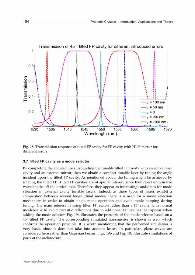
A last point to mention about the tilted FP cavity is the sensitivity of the design to fabrication errors. Considering a HLH combination for both mirrors, and introducing errors from 100 nm down to -100 nm in steps of 50 nm, we notice from Fig. 18 that the resonance wavelength shifts by about ±7 nm for an increase of ±50 nm. Also, the FWHM increases from 0.18 nm for the error free design to 0.25 nm for an introduced error of 50 nm. It reaches 0.55 nm for an introduced error of 100 nm. Thus, the structure is not very tolerant to fabrication errors and the filter shall be designed, fabricated and tested carefully before integration into optical systems.
1520 1530 1540 1550 1560 1570 15800
0.2
0.4
0.6
0.8
1Transmission response of tilted FP cavity under different angles of incidence
Wavelength (nm)
Tra
nsm
issio
n
inc
= 46
inc = 45.5
inc
= 45
inc = 44.5
inc
= 44
Fig. 17. Transmission response of tilted FP cavity in HLH configuration under different angles of incidence
www.intechopen.com
Photonic Crystals – Introduction, Applications and Theory
104
1530 1535 1540 1545 1550 1555 1560 1565 15700
0.2
0.4
0.6
0.8
1Transmission of 45 tilted FP cavity for different introduced errors
Wavelength (nm)
Tra
nsm
issio
n
= 100 nm
= 50 nm
= 0
= -50 nm
= -100 nm
Fig. 18. Transmission response of tilted FP cavity for FP cavity with HLH mirror for different errors.
3.7 Tilted FP cavity as a mode selector
By completing the architecture surrounding the tunable tilted FP cavity with an active laser
cavity and an external mirror, then we obtain a compact tunable laser by tuning the angle
incident upon the tilted FP cavity. As mentioned above, the tuning might be achieved by
rotating the tilted FP. Tilted FP cavities are of special interest, since they reject undesirable
wavelengths off the optical axis. Therefore, they appear as interesting candidates for mode
selection in external cavity tunable lasers. Indeed, as these types of lasers exhibit a
competition between several longitudinal modes, there is a need for a mode selection
mechanism in order to obtain single mode operation and avoid mode hopping during
tuning. The main interest in using tilted FP etalon rather than a FP cavity with normal
incidence is to avoid parasitic reflections due to additional FP cavities that appear when
adding the mode selector. Fig. 19a illustrates the principle of the mode selector based on a
45° tilted FP cavity. The corresponding simulated transmission is shown as well, which
confirms the operation principle. It is worth mentioning that the performed simulation is
very basic, since it does not take into account losses. In particular, plane waves are
considered here rather than Gaussian beams. Figs. 19b and Fig. 19c illustrate simulations of
parts of the architecture.
www.intechopen.com

MEMS Based Deep 1D Photonic Crystal
105
1500 1510 1520 1530 1540 1550 1560 1570 1580 1590 1600-90
-80
-70
-60
-50
-40
-30
-20
-10
0
in m
Tra
nsm
itta
nc
e a
nd
Re
fle
cta
nce
in
dB
Transmission Response for Laser Diode interface + Air Cavity + Mode Selector tilted at 45
Transmittance
Reflectance
(a)
1500 1510 1520 1530 1540 1550 1560 1570 1580 1590 1600-50
-45
-40
-35
-30
-25
-20
-15
-10
-5
0
in m
Tra
ns
mit
tan
ce
in
dB
Transmission Response for Laser Diode interface + Air Gap + 1st mirror of the Mode Selector
Transmittance
Reflectance
(b)
Mode selector
Tilted FP cavityInP layer
n = 3.1649
d=100 µm L=80 µm
Gap g = 2.2 µm
Transmission
Reflection
Mode selector
Tilted FP cavityInP layer
n = 3.1649
d=100 µm L=80 µm
Gap g = 2.2 µm
Transmission
Reflection
Tilted, Single
Bragg mirrorInP layer
n = 3.1649
d=100 µm L=80 µm
Transmission
Reflection
Tilted, Single
Bragg mirrorInP layer
n = 3.1649
d=100 µm L=80 µm
Transmission
Reflection
www.intechopen.com

Photonic Crystals – Introduction, Applications and Theory
106
1540 1545 1550 1555 1560 1565 1570 1575 1580-80
-70
-60
-50
-40
-30
-20
-10
0
in m
Tra
nsm
itta
nc
e a
nd
Refl
ec
tan
ce i
n d
B
Transmission and Reflectance for the Mode Selector "tilted Fabry-Perot cavity" based on a 7 layer Bragg mirror
Transmittance
Reflectance
(c)
Fig. 19. Tilted FP etalon as a laser mode selector. Whole systems (a) and parts of the system (b) and (c)
1563 1564 1565 1566 1567 1568 1569 1570 1571 1572-70
-60
-50
-40
-30
-20
-10
0
in m
Tra
nsm
itta
nce
in
dB
Transmission Response for Laser Diode interface + Air Cavity + Mode Selector
X: 1566
Y: -1.421
X: 1567
Y: -0.1047X: 1568
Y: -0.5737Gap = 2.2 m
Gap = 2.2 m + 5 nm
Gap = 2.2 m - 5 nm
(a)
Mode selector
Tilted FP cavity
Gap g = 2.2 µm
Transmission
Reflection
Mode selector
Tilted FP cavity
Gap g = 2.2 µm
Transmission
Reflection
www.intechopen.com

MEMS Based Deep 1D Photonic Crystal
107
2120 2140 2160 2180 2200 2220 2240 2260 22801550
1555
1560
1565
1570
1575
1580
1585
Gap separation for the tilted cavity in nm
Wa
vele
ng
th i
n n
m
Wavelength Tuning versus variation in the gap of the tilted cavity
(b)
1564 1564.5 1565 1565.5 1566 1566.5 1567 1567.5 1568 1568.5 1569-70
-60
-50
-40
-30
-20
-10
0
in m
Tra
nsm
itta
nce in
dB
Transmission Response for Laser Diode interface + Air Cavity + Mode Selector
Air Cavity = 100 m
Air Cavity = 90 m
Air Cavity = 80 m
(c)
Fig. 20. (a) and (b) Simulated wavelength tuning by control of the gap g of the tilted FP cavity (c) no wavelength shift is noticed when varying the distance L between the mode selector and the InP layer.
www.intechopen.com
Photonic Crystals – Introduction, Applications and Theory
108
Tuning is achieved either by rotating the cavity further or by controlling its gap g, as
shown in Figs. 20a and 20b. Tuning range of 30 nm is shown as the result of gap tuning of
150 nm. The increase in the separation distance L doesn’t affect the peak position as
shown in Fig. 20c.
4. Advanced FP architecture
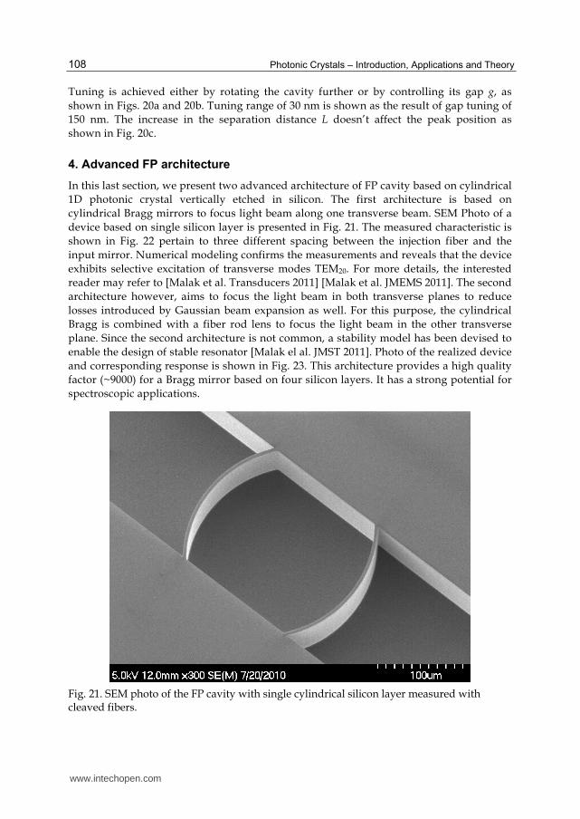
In this last section, we present two advanced architecture of FP cavity based on cylindrical
1D photonic crystal vertically etched in silicon. The first architecture is based on
cylindrical Bragg mirrors to focus light beam along one transverse beam. SEM Photo of a
device based on single silicon layer is presented in Fig. 21. The measured characteristic is
shown in Fig. 22 pertain to three different spacing between the injection fiber and the
input mirror. Numerical modeling confirms the measurements and reveals that the device
exhibits selective excitation of transverse modes TEM20. For more details, the interested
reader may refer to [Malak et al. Transducers 2011] [Malak et al. JMEMS 2011]. The second
architecture however, aims to focus the light beam in both transverse planes to reduce
losses introduced by Gaussian beam expansion as well. For this purpose, the cylindrical
Bragg is combined with a fiber rod lens to focus the light beam in the other transverse
plane. Since the second architecture is not common, a stability model has been devised to
enable the design of stable resonator [Malak el al. JMST 2011]. Photo of the realized device
and corresponding response is shown in Fig. 23. This architecture provides a high quality
factor (~9000) for a Bragg mirror based on four silicon layers. It has a strong potential for
spectroscopic applications.
Fig. 21. SEM photo of the FP cavity with single cylindrical silicon layer measured with cleaved fibers.
www.intechopen.com

MEMS Based Deep 1D Photonic Crystal
109
0
0.2
0.4
0.6
0.8
1
1528 1533 1538 1543
Wavelength (nm)
Norm
aliz
ed o
utp
ut pow
er
Zin = 150 μmZin = 300 μmZin = 460 μm
TEM00 TEM20
(a)
(b)
(c)
0
0.1
0.2
0.3
0.4
0.5
0.6
0.7
0.8
0.9
1
-30 -20 -10 0 10 20 30
X position (μm)
Norm
aliz
ed P
ow
er
0
0.1
0.2
0.3
0.4
0.5
0.6
0.7
0.8
0.9
1
-30 -20 -10 0 10 20 30
X position (um)
No
rma
lize
d P
ow
er
Fig. 22. Highlights on “Wavelength selective switching” and “Mode selective filtering” of the curved FP cavity (a) Recorded spectral response of the cavity, measured with lensed fiber while varying the fiber-to-cavity distance D. The quasi-periodic pattern of the curve reveals selective excitation of the resonant transverse modes TEM20 around 1532 nm in addition to the fundamental Gaussian mode TEM00. Varying the distance D leads to different levels for mode TEM20 with an extinction ratio of 7:1, the maximum amplitude was at D=150 µm. (b) Ideal intensity distribution of TEM00 and TEM20 modes. (c) Measured intensity profiles (of modes TEM00 and TEM20) obtained by lateral in-plane scanning of the detection fiber.
www.intechopen.com

Photonic Crystals – Introduction, Applications and Theory
110
INPUT
fiber
groove
OUTPUT
fiber
groove
Curved Bragg
reflector
Fib
er R
od
Len
sF
iber R
od
Len
s
(a)
1555.5 1556 1556.5 1557 1557.5
-40
-38
-36
-34
-32
-30
-28
-26
-24
-22
Wavelength in nm
Tra
nsm
itte
d P
ow
er
in d
B
1556.2 1556.3 1556.4
-26
-25
-24
-23
3-dB = 0.177 nm
(b)
Fig. 23. (a) Top view of the curved FP cavity with the fiber rod lens (b) Typical response obtained from such device
5. Concluding remarks
1D photonic crystal structure acquired a high interest long ago due to the application
domain they touch. As outlined in this chapter, they constitute a basic building block in
many devices like FP resonators, multilayered coating. The attractiveness in them comes
from their easy design and modeling based on multilayered stack theory and the affordable
fabrication process, thanks to the advance in the fabrication processes, in particular, the
advance in the DRIE process which helped producing vertical Bragg on silicon. In this
context, this chapter focused on specific issues concerning 1D photonic crystal: design and
www.intechopen.com

MEMS Based Deep 1D Photonic Crystal
111
modeling, fabrication technology, common applications and a brief introduction to an
advanced application: The curved FP cavity.
6. References
Lipson, A. & Yeatman, E.M. (2005). Free-Space MEMS tunable optical filter on (110) silicon, IEEE/LEOS International Conference on Optical MEMs and Their Applications, Oulu, Finland, 1-4 August pp. 73-74
Lipson, A. & E. Yeatman, E. M. (2007). A 1-D Photonic Band Gap Tunable Optical Filter in (110) Silicon, Journal of Microelectromechanical Systems, vol. 16, no.3, pp. 521- 527.
Macleod, H. A. (2001). Thin Film Optical Filters, ISBN 0 7503 0688 2, London, UK Malak, M.; Pavy, N.; Marty, F.; Peter, Y.-A.; Liu, A. Q. & Bourouina, T. (2011).
Micromachined Fabry–Perot resonator combining submillimeter cavity length and high quality factor, Applied Physics Letters, vol 98, 211113/1-3.
Malak, M.; Pavy, N.; Marty F. & Bourouina, T. (2011). Mode-Selective Optical Filtering And Wavelength-Selective Switching Through Fabry-Perot Cavity With Cylindrical Reflectors, 16th International Conference on Solid-State Sensors, Actuators and Microsystems (TRANSDUCERS), pp. 534-537.
Malak, M.; Pavy,N.; Marty, F.; Peter, Y.-A.; Liu, A. Q. & Bourouina, T. Cylindrical Surfaces Enable Wavelength-Selective Extinction and Sub-0.2 nm Linewidth in 250 µm-Gap Silicon Fabry-Pérot Cavities, submitted to the Journal of Microelectromechanical systems.
Malak, M.; Pavy,N.; Marty, F.; Richalot, E.; Liu, A. Q. & Bourouina, T. (2011) Design, modeling and characterization of stable, high Q-factor curved Fabry–Perot cavities, Journal of Microsystem Technologies, vol 17, no 4, pp. 543-552
Marty, F.; Rousseau, L.; Saadany, B.; Mercier, B.; Français, O.; Mita, Y. & Bourouina, T. (2005). Advanced Etching of Silicon Based On Deep Reactive Ion Etching For Silicon High Aspect Ratio Micro Structures And Three-Dimensional Micro- And Nano-Structures, Microelectronics Journal, vol. 36, pp. 673-677.
Pruessner, M.W.; Stievater, T.H. & Rabinovich, W.S. (2008). Reconfigurable Filters Using MEMS Resonators and Integrated Optical Microcavities, IEEE MEMS conference, pp.766-769.
Saadany, B.; Malak, M.; Kubota, M.; Marty, F.; Mita, Y.; Khalil, D. & Bourouina, T. (2006). Free-space Tunable and Drop Optical Filters Using Vertical Bragg Mirrors on Silicon, IEEE Journal of Selected Topics in Quantum Electronics, vol 12, no. 6, pp.1480-1488.
Yun, S. & Lee, J. (2003). A Micromachined In-Plane Tunable Optical Filter Using the Thermo-optic Effect of Crystalline Silicon, Journal of Micromechanics and Microengineering, vol. 13, pp.721-725.
Yun, S-S; You, S-K & Lee, J-H (2006). Fabrication of vertical optical plane using DRIE and KOH crystalline etching of (110) silicon wafer, Sensors Actuators A, vol. 128, pp. 387–394.
Song, I.-H. ; Peter, Y.-A. & Meunier, M. (2007). Smoothing dry-etched microstructure sidewalls using focused ion beam milling for optical applications, Journal of Micromechanics and Microengineering, vol. 17, pp.1593-1597.
www.intechopen.com

Photonic Crystals – Introduction, Applications and Theory
112
Zandi, K.; Wong, B.; Zou, J.; Kruzelecky, R. V.; Jamroz W. & Peter, Y.-A. (2010). In-Plane Silicon-On-Insulator Optical MEMS Accelerometer Using Waveguide Fabry-Perot Microcavity With Silicon/Air Bragg Mirrors, in Proc. 23rd IEEE Int. Conf. Micro Electro Mech. Syst., pp. 839-842.
www.intechopen.com

Photonic Crystals - Introduction, Applications and TheoryEdited by Dr. Alessandro Massaro
ISBN 978-953-51-0431-5Hard cover, 344 pagesPublisher InTechPublished online 30, March, 2012Published in print edition March, 2012
InTech EuropeUniversity Campus STeP Ri Slavka Krautzeka 83/A 51000 Rijeka, Croatia Phone: +385 (51) 770 447 Fax: +385 (51) 686 166www.intechopen.com
InTech ChinaUnit 405, Office Block, Hotel Equatorial Shanghai No.65, Yan An Road (West), Shanghai, 200040, China
Phone: +86-21-62489820 Fax: +86-21-62489821
The first volume of the book concerns the introduction of photonic crystals and applications including designand modeling aspects. Photonic crystals are attractive optical materials for controlling and manipulating theflow of light. In particular, photonic crystals are of great interest for both fundamental and applied research,and the two dimensional ones are beginning to find commercial applications such as optical logic devices,micro electro-mechanical systems (MEMS), sensors. The first commercial products involving two-dimensionally periodic photonic crystals are already available in the form of photonic-crystal fibers, which use amicroscale structure to confine light with radically different characteristics compared to conventional opticalfiber for applications in nonlinear devices and guiding wavelengths. The goal of the first volume is to providean overview about the listed issues.
How to referenceIn order to correctly reference this scholarly work, feel free to copy and paste the following:
Maurine Malak and Tarik Bourouina (2012). MEMS Based Deep 1D Photonic Crystal, Photonic Crystals -Introduction, Applications and Theory, Dr. Alessandro Massaro (Ed.), ISBN: 978-953-51-0431-5, InTech,Available from: http://www.intechopen.com/books/photonic-crystals-introduction-applications-and-theory/mems-based-deep-1d-photonic-crystal

© 2012 The Author(s). Licensee IntechOpen. This is an open access articledistributed under the terms of the Creative Commons Attribution 3.0License, which permits unrestricted use, distribution, and reproduction inany medium, provided the original work is properly cited.