MEMS ACCELEROMETERS AND GYROSCOPES FOR INERTIAL ...etd.lib.metu.edu.tr/upload/12605331/index.pdf ·...
157
MEMS ACCELEROMETERS AND GYROSCOPES FOR INERTIAL MEASUREMENT UNITS A THESIS SUBMITTED TO THE GRADUATE SCHOOL OF NATURAL AND APPLIED SCIENCES OF MIDDLE EAST TECHNICAL UNIVERSITY BY MEHMET AKİF ERİŞMİŞ IN PARTIAL FULFILLMENT OF THE REQUIREMENTS FOR THE DEGREE OF MASTER OF SCIENCE IN ELECTRICAL AND ELECTRONICS ENGINEERING SEPTEMBER 2004
Transcript of MEMS ACCELEROMETERS AND GYROSCOPES FOR INERTIAL ...etd.lib.metu.edu.tr/upload/12605331/index.pdf ·...
MEMS ACCELEROMETERS AND GYROSCOPES
FOR
INERTIAL MEASUREMENT UNITS
A THESIS SUBMITTED TO
THE GRADUATE SCHOOL OF NATURAL AND APPLIED SCIENCES
OF
MIDDLE EAST TECHNICAL UNIVERSITY
BY
MEHMET AKİF ERİŞMİŞ
IN PARTIAL FULFILLMENT OF THE REQUIREMENTS
FOR
THE DEGREE OF MASTER OF SCIENCE
IN
ELECTRICAL AND ELECTRONICS ENGINEERING
SEPTEMBER 2004
Approval of Graduate School of Natural and Applied Science.
_____________________________ Prof. Dr. Canan ÖZGEN
Director
I certify that this thesis satisfies all the requirements as a thesis for the degree of
Master of Science.
_____________________________
Prof. Dr. Mübeccel DEMİREKLER
Head of Department
This is to certify that we have read this thesis and that in our opinion it is fully
adequate, in scope and quality, as a thesis for the degree of Master of Science.
____________________________
Prof. Dr. Tayfun AKIN
Supervisor
Examining Committee Members: Prof. Dr. Cengiz BEŞİKÇİ (METU, EEE)
____________________________
Prof. Dr. Tayfun AKIN (METU, EEE)
____________________________
Prof. Dr. Aydan ERKMEN (METU, EEE)
____________________________
Instructor Dr. Haluk KÜLAH (METU, EEE)
____________________________
Dr. Volkan NALBANTOĞLU (ASELSAN)
____________________________

iii
I hereby declare that all information in this document has been obtained and
presented in accordance with academic rules and ethical conduct. I also declare that,
as required by these rules and conduct, I have fully cited and referenced all material
and results that are not original to this work.
Mehmet Akif ERİŞMİŞ
iv
ABSTRACT
MEMS ACCELEROMETERS AND GYROSCOPES FOR
INERTIAL MEASUREMENT UNITS
Erişmiş, Mehmet Akif
M.Sc., Department of Electrical and Electronics Engineering
Supervisor: Prof. Dr. Tayfun Akın
September 2004, 137 pages
This thesis reports the development of micromachined accelerometers and
gyroscopes that can be used for micromachined inertial measurement units (IMUs).
Micromachined IMUs started to appear in the market in the past decade as low cost,
moderate performance alternative in many inertial applications including military,
industrial, medical, and consumer applications. In the framework of this thesis, a
number of accelerometers and gyroscopes have been developed in three different
fabrication processes, and the operation of these fabricated devices is verified with
extensive tests. In addition, the fabricated accelerometers were combined with
external readout electronics to obtain hybrid accelerometer systems, which were
tested in industrial test facilities.
The accelerometers and gyroscopes are designed and optimized using the MATLAB
analytical simulator and COVENTORWARE finite element simulation tool. First set
of devices is fabricated using a commercial foundry process called SOIMUMPs,
while the second set of devices is fabricated using the electroplating processes
v
developed at METU-MET facilities. The third set of devices is designed for a new
advanced process based on DRIE, which is under development.
Mechanical and electrical test results of the fabricated accelerometers and
gyroscopes are in close agreement with the designed values. The testing of the SOI
and nickel accelerometers is also performed in industrial test environments. In order
to perform these tests, accelerometers are hybrid connected to commercially
available capacitive readout circuits. These accelerometer systems require only two
DC supply voltages for operation and provide an analog output voltage related to the
input acceleration. The industrial tests show that the SOI accelerometer system
yields a 799 µg/√Hz average noise floor, a 1.8 mg/√Hz peak noise floor, a 22.2 mV/g
sensitivity, and a 0.1 % nonlinearity, while the nickel accelerometer system yields a
228 µg/√Hz average noise floor, a 375 µg/√Hz peak noise floor, a 1.02 V/g
sensitivity, and a 0.23 % nonlinearity. Long-term drift components of the
accelerometers are determined to be smaller than 20 mg. These systems are the
highest performance micromachined accelerometer systems developed in Turkey,
and they can be used in implementation of a national inertial measurement unit.
Keywords: Accelerometer, Gyroscope, Inertial Measurement Unit, Micro-Electro-
Mechanical Systems (MEMS), and micromachined inertial devices.
vi
ÖZ
ATALETSEL ÖLÇÜM BİRİMİ İÇİN MEMS
İVMEÖLÇERLER VE DÖNÜÖLÇERLER
Erişmiş, Mehmet Akif
Yüksek Lisans, Elektrik ve Elektronik Mühendisliği Bölümü
Tez Yöneticisi: Prof. Dr. Tayfun Akın
Eylül 2004, 137 sayfa
Bu tez ataletsel ölçüm biriminde (IMU) kullanılabilecek mikroişlenmiş ivmeölçerler
ve dönüölçerler geliştirilmesini rapor etmektedir. Mikroişlenmiş IMU’lar,
endüstriyel, medikal ve tüketici uygulamalarında, düşük maliyetli ve yüksek
performanslı alternatifler olarak kullanılmaya başlanmıştır. Bu tez çalışması
kapsamında çok sayıda ivmeölçer ve dönüölçer üç farklı üretim süreci kullanılarak
geliştirilmiş, ayrıca yapılan çeşitli testlerle ürünlerin istenilen şekilde çalıştıkları
gösterilmiştir. Buna ek olarak, tez kapsamında üretilmiş olan ivmeölçerler, dış
okuma devreleri ile birleştirilerek hibrit ivmeölçer sistemleri tasarlanmış ve bu
sistemler endüstriyel test alanlarında test edilmiştir.
İvmeölçerler ve dönüölçerler MATLAB analitik simülatör ve COVENTORWARE
sonlu eleman simülatörü ile tasarlanmış ve en iyilenmiştir. İlk grup ürünler
SOIMUMPs adlı ticari bir üretim süreci ile üretilirken, ikinci grup ürünler METU-
MET tesislerinde geliştirilen elektrokaplama yöntemi ile üretilmiştir. Üçüncü grup
ürünler halen geliştirilmekte olan DRIE bazlı yeni ve gelişmiş bir ürün süreci için
tasarlanmıştır.

vii
Üretilen ivmeölçerler ile dönüölçerlerin mekanik ve elektriksel test sonuçları
tasarlanan değerlere çok yakın çıkmıştır. SOI ve nikel ivmeölçerlerin testleri
endüstriyel ortamlarda da gerçekleştirilmiştir. Bu testleri gerçekleştiribilmek için
ivmeölçerler, endüstriyel bir kapasitif okuma devrelerine hibrit bağlanmıştır. Bu
ivmeölçer sistemleri sadece iki DC voltaj kaynağı ile beslenmekte ve ölçülen
ivmeyle orantılı analog voltaj çıkışı vermektedir. Endüstriyel testler, SOI ivmeölçer
sisteminin 799 µg/√Hz ortalama gürültü seviyesi, 1.8 mg/√Hz tepe gürültü seviyesi,
22.2 mV/g orantı katsayısı, ve % 0.1 orantı katsayısı hatası olduğunu ve nikel
ivmeölçer sisteminin 228 µg/√Hz ortalama gürültü seviyesi, 375 µg/√Hz tepe gürültü
seviyesi, 1.02 V/g orantı katsayısı, % 0.23 orantı katsayısı hatası olduğunu
göstermiştir. Uzun süreli sabit kayma ile açış-kapanış sabit kayma değerlerinin
20 mg’den küçük olduğu bulunmuştur. Bu sistemler Türkiye’de üretilen en yüksek
performanslı mikroişlenmiş ivmeölçer sistemleri olup, ulusal ataletsel ölçüm birimi
geliştirilmesinde kullanılabilirler.
Anahtar Kelime: İvmeölçer, Jiroskop, Ataletsel Ölçüm Birimi, Mikroelektromekanik
Sistemler (MEMS) ve mikroişlenmiş ataletsel sensörler.

viii
To my family
ix
ACKNOWLEDGEMENTS
First of all, I would like to thank my family for their love and support. I would
specially like to thank my advisor Prof. Dr. Tayfun Akın for his guidance and
support, and especially for his friendly attitude.
I would like to thank Mr. Said Emre Alper and Mr. Fırat Yazıcıoğlu for sharing their
knowledge with me, for helping me especially in fabrication steps, and for their
patience to my endless questions. I would like to thank Mr. Orhan Akar for his
suggestions in the fabrication process and for wire bonding sessions. I would like to
thank our group computer administrator Mr. Murat Tepegöz for his time spent on
constructing and maintenance of our group’s computer network. I would like to
acknowledge all METU-MEMS group members for providing a nice research
atmosphere. I would like to thank METU-MET personnel for their help in the
fabrication steps. Also, I would like to thank all my friends for their support and
friendship. I would like to thank TUBITAK-SAGE and ASELSAN for providing
their test facilities, and finally I would like to thank ASELSAN for SEM pictures.

x
TABLE OF CONTENTS
PALAGIARISM …………………………………………………………………….iii
ABSTRACT ……...…………………………………………………………………iv
ÖZ ……………………………………………………………………………….…..vi
DEDICATION …..…………………………………………………………………viii
ACKNOWLEDGEMENTS …………………………………………………………ix
TABLE OF CONTENTS …………………………………………………………….x
LIST OF FIGURES ………………………………………………………………..xiii
LIST OF TABLES …………………………………………………………………xix
1. INTRODUCTION ............................................................................................. 1
1.1 BASIC OPERATION PRINCIPLES OF ACCELEROMETERS AND GYROSCOPES........... 6
1.2 CLASSIFICATION OF MEMS ACCELEROMETERS AND GYROSCOPES .................... 7
1.3 OBJECTIVES OF THE STUDY AND THE ORGANIZATION OF THE THESIS ............... 10
2. THEORETICAL BACKGROUND ............................................................... 13
2.1 DEFINITIONS OF SOME COMMONLY USED MECHANICAL TERMS ...................... 13
2.2 DERIVATION OF SPRING CONSTANT FOR VARIABLE SPRING SHAPES ................ 16
2.3 CORIOLIS FORCE ............................................................................................... 20
2.4 ACCELEROMETER AND GYROSCOPE MODELS ................................................... 21
2.4.1 Accelerometer Model................................................................................ 21
2.4.2. Gyroscope Model ..................................................................................... 27
2.5 DIFFERENT CAPACITIVE SENSING AND ACTUATING TOPOLOGIES ..................... 32
2.5.1 Capacitance Basics.................................................................................... 32

xi
2.5.2 Parallel Plate Capacitance Configuration.................................................. 33
2.5.3 Transverse Comb Capacitance Configuration .......................................... 34
2.5.4 Lateral Comb Capacitance Configuration................................................. 36
2.6 SUMMARY ......................................................................................................... 37
3. MEMS ACCELEROMETERS AND GYROSCOPES DESIGN................ 38
3.1 DESIGN PARAMETERS AND CHALLENGES FOR MEMS ACCELEROMETERS........ 38
3.2 DESIGN PARAMETERS AND CHALLENGES FOR MEMS GYROSCOPES ................ 41
3.3 ACCELEROMETERS AND GYROSCOPES DESIGNED IN THIS STUDY..................... 42
3.3.1 Accelerometer Topology........................................................................... 43
3.3.2 Gyroscope Topology................................................................................. 48
3.3.3 Design Considerations for Three Different Processes .............................. 53
3.3.4 Performance Estimations for the Designed Accelerometers and
Gyroscopes......................................................................................................... 55
3.4 SUMMARY ......................................................................................................... 62
4. MEMS ACCELEROMETERS AND GYROSCOPES FABRICATION... 63
4.1 INTRODUCTION TO MEMS FABRICATION TECHNIQUES .................................... 63
4.2 DETAILS OF SOIMUMPS PROCESS ................................................................... 65
4.3 DETAILS OF NICKEL ELECTROPLATING PROCESS .............................................. 70
4.3.1 Fabrication of Metallization Layer in Nickel Electroplating Process....... 75
4.3.2 Fabrication of Sacrificial Layer in Nickel Electroplating Process............ 76
4.3.3 Fabrication of Structural Layer in Nickel Electroplating Process ............ 77
4.4 DETAILS OF DRIE PROCESS .............................................................................. 79
4.4.1 Fabrication of Anchor Regions and Shield Metal in the DRIE Process ... 87
4.4.2 Anodic Bonding and Fabrication of Metallization Layer in the DRIE
Process ............................................................................................................... 89
4.4.3 Fabrication of Oxide Mask and DRIE Step in the DRIE Process............. 89
4.5 SUMMARY ......................................................................................................... 90
5. FABRICATION AND TEST RESULTS....................................................... 91
5.1 FABRICATION RESULTS OF EACH THREE PROCESSES ........................................ 91
5.1.1 Fabrication Results of SOIMUMPs Process ............................................. 92
5.1.2 Fabrication Results Nickel Electroplating Process ................................... 94
xii
5.1.3 Fabrication Results of DRIE Process........................................................ 96
5.2 BASIC TESTS PERFORMED ON THE ACCELEROMETER AND THE GYROSCOPE
SAMPLES ................................................................................................................. 98
5.3 OPEN LOOP TESTS OF ACCELEROMETERS AND MS3110 READOUT CIRCUITRY
HYBRID SYSTEM ................................................................................................... 113
5.4 SUMMARY AND DISCUSSION OF THE FABRICATION AND TEST RESULTS.......... 125
6. CONCLUSION AND SUGGESTIONS FOR FUTURE RESEARCH..... 127
REFERENCES .…………………………………………………………………. 132
xiii
LIST OF FIGURES
Figure 1.1: The application areas for accelerometers and the bandwidth-resolution
performances of the accelerometers for these applications [5, 11]...................... 3
Figure 1.2: Cost-bias instability performances of IMUs, [12]. .................................... 4
Figure 2.1: Stress-Strain relationship of a general material [26]. .............................. 15
Figure 2.2: A spring beam in its rest position. ........................................................... 17
Figure 2.3: Resultant spring constants for parallel and series springs. ...................... 18
Figure 2.4: Series connected half clamped beams forming a fixed-guided end beam.
............................................................................................................................ 18
Figure 2.5: Different spring structures used in this study and calculated resultant
spring constants.................................................................................................. 19
Figure 2.6: Coordinate system showing primary and secondary modes of a gyroscope
with a tuning fork gyroscope structure [3]......................................................... 21
Figure 2.7: Accelerometer mass-spring-damper model. ............................................ 22
Figure 2.8: Accelerometer proof mass displacement under a constant amplitude
acceleration versus acceleration frequency........................................................ 24
Figure 2.9: Focused view of the linear response region and the response error. ....... 24
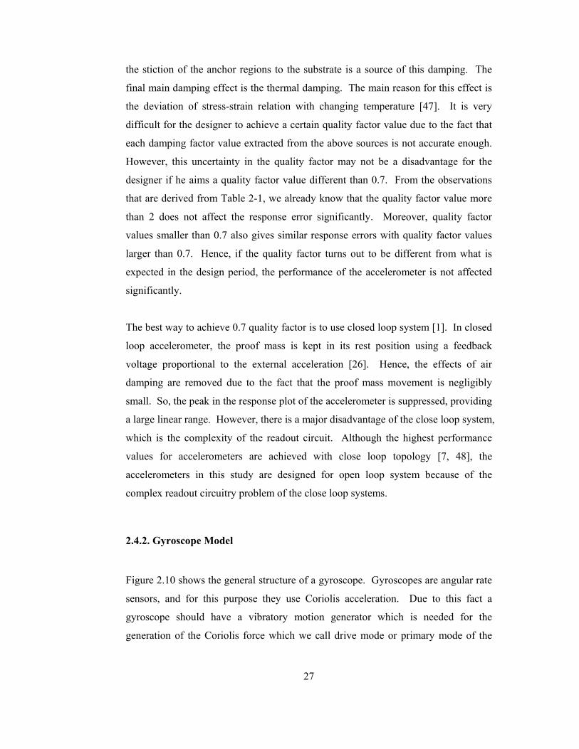
Figure 2.10: General structure of a gyroscope. The gyroscope is composed of an
actuator part which creates the primary vibration, and an accelerometer part
which senses Coriolis acceleration due to external rotation. ............................. 28
Figure 2.11: Different coupling modes of the gyroscopes. (a) shows the simplest
configuration where the drive mode and the sense mode affects each other
directly. (b) shows a more advanced configuration where the drive mode
motion cannot be affected by the sense mode because it has only 1 degree of
freedom (DOF) while it affects the sense mode. (c) shows the most advanced
xiv
configuration where drive and sense modes have only 1 DOF and they are
attached to each other with a 2 DOF proof mass [49]. ...................................... 29
Figure 2.12: Three different frequency choices of the gyroscopes. (a) does not need
any external circuit to compensate response error but this choice is not practical
due to very low output signals. (b) shows mismatched resonance frequencies
case and (c) shows matched resonance frequencies case. (c) shows a larger
response compared to (b) but (b) has a wider 3dB bandwidth........................... 31
Figure 2.13: Parallel plate configuration.................................................................... 33
Figure 2.14: Transverse comb configuration: (a) before movement and (b) after
movement........................................................................................................... 35
Figure 2.15: Lateral comb configuration: (a) before movement and (b) after
movement........................................................................................................... 36
Figure 3.1: The topology of the designed accelerometers, which is the lateral
accelerometer topology. ..................................................................................... 45
Figure 3.2: Two different configurations that can be used in accelerometers: (a)
Transverse comb capacitive configuration, (b) simplified transverse comb
capacitance configuration................................................................................... 46
Figure 3.3: FEM simulation results for determining the resonance modes of the
accelerometer topology: (a) the desired sensitivity mode, (b) the unwanted
cross mode.......................................................................................................... 47
Figure 3.4: The topology of the designed gyroscope. The proof mass has 2DOF
(degree of freedom) while sense and drive mode electrodes have 1DOF. Drive
electrodes mechanically cannot move in the sense mode, and sense electrodes
mechanically cannot move in the drive mode due to the decoupled mechanical
design of the gyroscope...................................................................................... 48
Figure 3.5: Simulation result of sense mode of the gyroscope using CoventorWare
FEM simulator. Drive mode electrodes do not move in the sense mode
verifying the decoupled operation...................................................................... 51
Figure 3.6: Simulation result of drive mode of the gyroscope using CoventorWare
FEM simulator. Sense mode electrodes do not move in the drive mode
verifying the decoupled operation...................................................................... 52
xv
Figure 3.7: Cross mode of the gyroscope topology. This mode is an unwanted mode
and the resonance frequency of this mode should be as far as possible from the
drive/sense mode resonance frequencies. .......................................................... 53
Figure 4.1: The overview of SOIMUMPs process [58]............................................. 68
Figure 4.2: The overall layout of SOIMUMPs chip. The chip includes
accelerometers and gyroscopes for this study and also some test structures and a
gyroscope for another study. The chip occupies 10mm x 10mm total chip area.
............................................................................................................................ 69
Figure 4.3: Overall fabrication details of nickel electroplating process. ................... 74
Figure 4.4: The overall layout of the nickel electroplating wafer. The chip is a 4 inch
wafer including several accelerometers and gyroscopes for this study and also
gyroscopes for another study. The sensors are placed into 3mm x 3mm die
areas. After the process, these dies are separated using a dicer machine.......... 75
Figure 4.5: Overall fabrication details of the DRIE process...................................... 85
Figure 4.6: The overall layout of the DRIE wafer. This is a 4-inch wafer including
several accelerometers and gyroscopes for this study and also gyroscopes for
another study. The sensors are placed into 4mm x 4mm die areas. .................. 87
Figure 5.1: SOIMUMPs accelerometers. Due to thicker features, the accelerometer
samples do not suffer from transportation problems.......................................... 92
Figure 5.2: Broken SOIMUMPs gyroscope structures. ............................................. 93
Figure 5.3: A fabricated nickel electroplated accelerometer and the deformation in
the spring regions. .............................................................................................. 95
Figure 5.4: SEM pictures of fabricated nickel electroplated accelerometers............. 95
Figure 5.5: A photograph of fabricated nickel electroplated gyroscope.................... 96
Figure 5.6: SEM picture of a DRIE gyroscope. The structure is 200 µm thick........ 97
Figure 5.7: SEM pictures of DRIE samples. (a) The critical structures are damaged
due to notching effect. (b) The etching in small openings is not finished. ....... 98
Figure 5.8: Resonance frequency test setup............................................................. 100
Figure 5.9: Capacitance test result of accelerometer prototype-1. The pull-in voltage
is measured as 25 V. ........................................................................................ 101
Figure 5.10: Capacitance test result of accelerometer prototype-2. The pull-in
voltage is measured as 16V.............................................................................. 101
xvi
Figure 5.11: Capacitance test result of accelerometer prototype-3. The pull-in
voltage is measured as 5.2 V............................................................................ 102
Figure 5.12: Capacitance test result of accelerometer prototype-4. The pull-in
voltage is measured as 8.8V............................................................................. 102
Figure 5.13: Capacitance test result of accelerometer prototype-5. The pull-in
voltage is measured as 12V.............................................................................. 103
Figure 5.14: Capacitance test result of accelerometer prototype-6. The pull-in
voltage is measured as 10V.............................................................................. 103
Figure 5.15: Capacitance test result of gyroscope prototype-1. The pull-in voltage is
measured as 19V. ............................................................................................. 104
Figure 5.16: Capacitance test result of gyroscope prototype-2. The pull-in voltage is
measured as 24V. ............................................................................................. 104
Figure 5.17: Resonance frequency test result of accelerometer prototype-1. The
measured resonance frequency is 31.3 kHz. The upper and lower pictures show
the magnitude and phase response, respectively. The frequency value shown on
top right of the each display window shows the resonance frequency value of
the sensor. Theoretically, the magnitude response should make a sharp decrease
after making a peak value, and the phase response should decrease and stay at
its low value. However, due to parasitic effects theoretical results cannot be
obtained. ........................................................................................................... 106
Figure 5.18: Resonance frequency test result of accelerometer prototype-2. The
measured resonance frequency is 12.51 kHz. .................................................. 107
Figure 5.19: Resonance frequency test result of accelerometer prototype-3.
Measured resonance frequency is 3.65 kHz..................................................... 107
Figure 5.20: Resonance frequency test result of accelerometer prototype-4.
Measured resonance frequency is 2.55 kHz..................................................... 108
Figure 5.21: Resonance frequency test result of accelerometer prototype-5.
Measured resonance frequency is 2.09 kHz..................................................... 108
Figure 5.22: Resonance frequency test result of accelerometer prototype-6.
Measured resonance frequency is 1.48 kHz..................................................... 109
Figure 5.23: Resonance frequency test result of the drive mode of prototype-1, which
is the SOIMUMPs gyroscope. The measured resonance frequency is 14.87 kHz.
xvii
In the drive mode of the gyroscope, theoretically the magnitude response makes
a step instead of a peak, and the phase response makes a peak instead of a step.
This is due to the configuration of the drive mode capacitances. In this figure,
the phase response indeed makes a peak; however, this peak cannot be observed
clearly due to 360° phase change. This is a display error due to network
analyzer. One of the reasons for this error is low capacitance values due to
process limitations and broken sense comb fingers. ........................................ 110
Figure 5.24: Resonance frequency test result of the sense mode of prototype-1. The
measured resonance frequency is 14.65 kHz. Sense mode magnitude/phase
response is similar to that of the accelerometers.............................................. 111
Figure 5.25: Resonance frequency test result of the drive mode of prototype-2, which
is a nickel gyroscope. The measured resonance frequency is 6.22 kHz. The
response is clearer than the response of SOIMUMPs sample, because this
sample has more sense capacitance and is connected to a buffer circuitry which
improves the output response........................................................................... 111
Figure 5.26: Resonance frequency test result of the sense mode of prototype-2. The
measured resonance frequency is 6.27 kHz. .................................................... 112
Figure 5.27: First generation hybrid accelerometer system that uses accelerometer
prototype-3 and MS3110 readout circuitry. ..................................................... 114
Figure 5.28: Block diagram of the first generation hybrid system. The system is
composed of the accelerometer and MS3110 switched-capacitor integrator type
differential capacitive readout circuit. The pole of low-pass-filter (LPF) also
determines 3dB bandwidth of the system. ....................................................... 114
Figure 5.29: The results of index table tests showing nonlinearity and sensitivity of
the first generation hybrid accelerometer system. The system shows less than
0.1 % nonlinearity and 22.2 mV/g sensitivity.................................................. 115
Figure 5.30: Noise test result of first generation hybrid accelerometer system.
Average noise level is found as 17.75 µV/√Hz which corresponds to
799 µg/√Hz. Peak noise floor is measured as 1.8 mg/√Hz. ............................ 116
Figure 5.31: The second generation hybrid accelerometer system. This system uses a
nickel accelerometer, and has bias circuitries and amplifier stages additional to
first generation hybrid system.......................................................................... 118

xviii
Figure 5.32: The block diagram of second generation hybrid system. The
instrumentation amplifier eliminates the DC offset of MS3110 and provides the
necessary voltage gain. Bias voltage generator provides the necessary bias
voltages to appropriate circuit blocks. ............................................................. 118
Figure 5.33:. Test results of second generation hybrid system using index table. The
system shows less than 0.1 % nonlinearity and almost 1 V/g sensitivity for
acceleration inputs in the range of ± 1g. .......................................................... 119
Figure 5.34: Test results of second generation hybrid system using rate table. The
system shows less than 0.3 % nonlinearity and almost 1 V/g sensitivity for high
acceleration inputs. The device is able to be tested in a range of (-3g, 6g)
acceleration inputs............................................................................................ 119
Figure 5.35: Noise test results of the second generation hybrid accelerometer system.
Average noise level is 228 µV/√Hz corresponding to 228 µg/√Hz, and peak
noise floor is measured as 375 µg/√Hz............................................................ 120
Figure 5.36: Bias drift test result of second generation hybrid accelerometer system.
The maximum average bias difference gives the run-to-run bias drift, and the
maximum long-term bias drift of each test result gives the long-term bias drift
of the system. The measured run-to-run bias drift and long-term bias drift of the
sensor are found as 16.6 mV and 19 mV corresponding to 16.6 mg and 19 mg,
respectively. ..................................................................................................... 122
Figure 5.37: The output variation due to temperature change for the second
generation accelerometer system. The output does not have exactly the same
value at the same temperature value for increasing and deceasing temperature
case. This error can be minimized with better packaging and with eliminating
potentiometers in the system............................................................................ 124
xix
LIST OF TABLES
Table 1-1: Range and bias stability requirements for gyroscopes for different
applications. [3-4]. .............................................................................................. 3
Table 1-2: Comparison of the applications and the priority of IMU properties for
these applications. ................................................................................................ 5
Table 1-3: The performance goals of the hybrid accelerometer system. ................... 11
Table 2-1: Response error of the accelerometer for 100 Hz accelerometer effective
bandwidth........................................................................................................... 26
Table 2-2: Definitions of performance metrics for capacitance configurations ........ 33
Table 2-3: Parallel plate capacitance configuration performance metrics. ................ 34
Table 2-4: Transverse comb capacitance configuration performance metrics.......... 36
Table 2-5: Lateral comb capacitance configuration performance metrics................. 37
Table 3-1: The comparison of stress formulation with the FEM simulations. It is
seen that the formulation result shows very similar results with the simulation
results, and the stress value decreases with increasing folded beam legs. ......... 45
Table 3-2: The summary of accelerometer prototype-1............................................. 55
Table 3-3: The summary of accelerometer-prototype-2 ............................................ 56
Table 3-4: The summary of the accelerometer prototype-3....................................... 56
Table 3-5: The summary of accelerometer prototype-4............................................. 57
Table 3-6: The summary of accelerometer prototype-5............................................. 57
Table 3-7: The summary of accelerometer prototype-6............................................. 58
Table 3-8: The summary of the accelerometer prototype-7....................................... 58
Table 3-9: The summary of accelerometer prototype-8............................................. 59
Table 3-10: The summary of the gyroscope prototype-1........................................... 60
Table 3-11: The summary of the gyroscope prototype-2........................................... 60
xx
Table 3-12: The summary of the gyroscope prototype-3........................................... 61
Table 3-13: The summary of the gyroscope prototype-4........................................... 61
Table 4-1: Thicknesses and purposes of material layers in SOIMUMPs process [58].
............................................................................................................................ 70
Table 4-2: Thicknesses and purposes of material layers in nickel electroplating
process................................................................................................................ 74
Table 4-3: Thicknesses and purposes of material layers in DRIE process. ............... 86
Table 5-1: The comparison of measured pull-in voltages with the designed values.
.......................................................................................................................... 105
Table 5-2: Comparison of capacitance and resonance frequency test results with the
designed values for the designed accelerometers............................................. 109
Table 5-3: Capacitance and resonance frequency test results for the designed
gyroscopes and comparison of these test results with the designed values. .... 112
Table 5-4: Comparison of measured and calculated noise levels of the first
generation hybrid system. There are two different electrical noise, and hence
total noise calculations. This is due to the electrical noise expression given in
MS3110 datasheet. The electrical noise is expressed as “Input capacitance
resolution” but it is not clear whether this resolution is single-ended or
differential. However, the measured noise floor show that the resolution
provided in the datasheet should be single-ended............................................ 117
Table 5-5: Comparison of calculated and measured noise levels of second generation
hybrid system. Two different electrical noises are calculated similar to the case
of first generation hybrid system. Single-ended resolution estimation yields a
closer total noise estimation. ............................................................................ 121
Table 5-6: Cross-axis sensitivity test results of second generation accelerometer
system. The sensitivity values are negligibly small. ....................................... 123
Table 5-7: The properties of second generation hybrid accelerometer system........ 124
Table 6-1: Comparison of design goals and achieved accelerometer performance
values. .............................................................................................................. 129

1
CHAPTER 1
INTRODUCTION
Tracking the position of an object is an important engineering problem that finds
many application areas including military, industrial, medical, and consumer
applications. This problem is effectively solved with an Inertial Measurement Unit
(IMU). An IMU consists of three orthogonally placed accelerometers and
gyroscopes, and these sensors find the linear acceleration and angular velocity of the
object that it is mounted on. Knowing linear acceleration and angular velocity in
three dimensions is enough to track the motion of the system with the help of
additional mathematical operations [1].
MEMS inertial sensors, accelerometers and gyroscopes, started to appear in the
market due to their low cost, small size, low power consumption, and promising
performances. Although these sensors initially fit for applications where cost and
size are more important than performance, currently their performances satisfy and
even extend beyond the limits of conventional sensing systems.
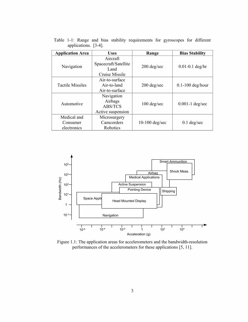
Performance requirements of inertial sensors vary for different applications. Table
1-1 shows the range and bias requirements for the gyroscopes, Figure 1.1 shows the
bandwidth-resolution performance requirements of the accelerometers for different
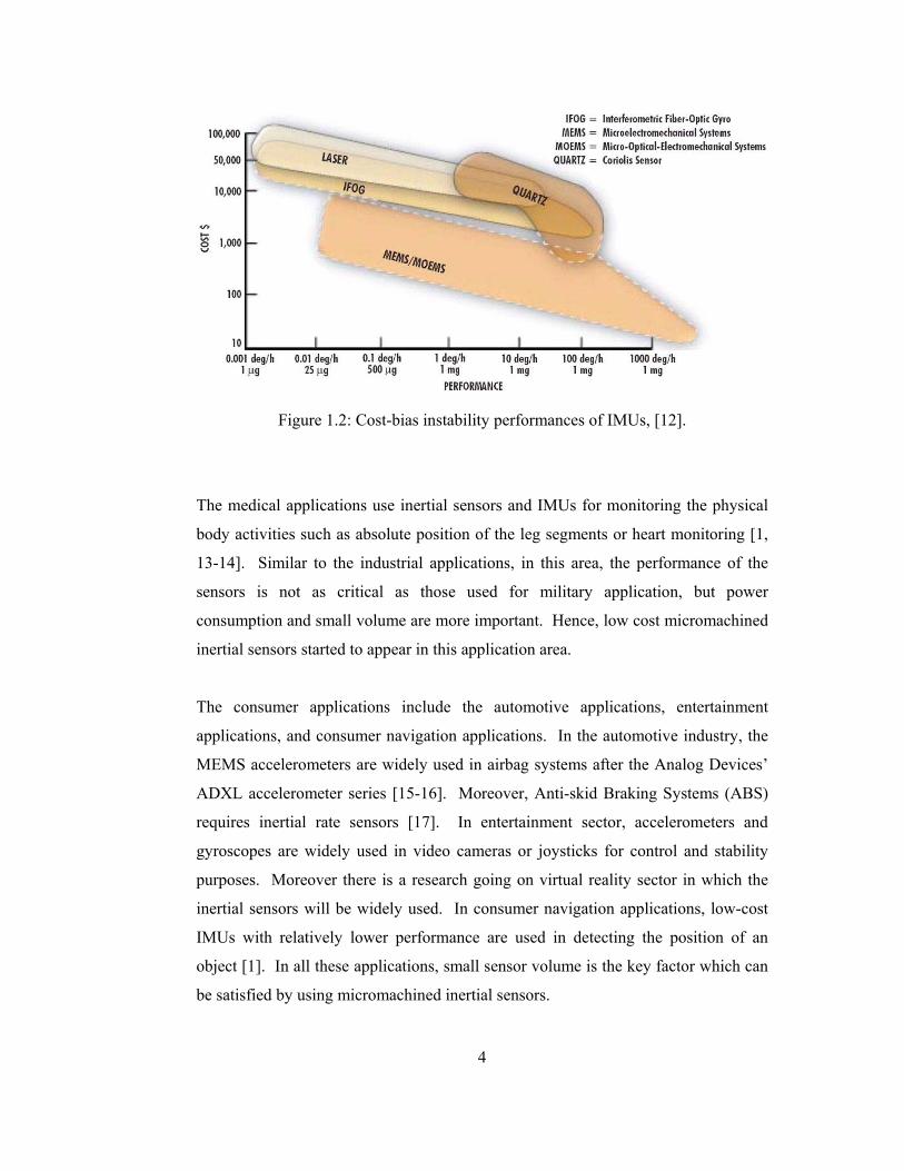
applications, and Figure 1.2 shows the cost-bias instability performances of IMUs.

2
In general, the highest performance is required for military applications. Military
navigation is the main application that pushes the development of higher
performance inertial sensors. Global Positioning System (GPS), which is developed
initially for military applications to track an object’s position with high accuracy,
combines the high performance IMUs, precision time references, radio
communications, and spaceborne satellite network to achieve a precise track of
motion [1-2]. The performances of the IMUs for military applications should be
superior compared to the ones used for other applications. The drift values should be
less then 0.1 deg/hour for the gyroscopes and in the order of few µg for
accelerometers to be used in navigation applications [3-5]. The fiber-optic
gyroscopes are used for these applications, but their fabrication is rather complicated
[4-6]. On the other hand, the performances of micromachined accelerometers and
gyroscopes are not far beyond the optical inertial sensors due to advances in
micromachining technologies in the past decade [7].
Industrial applications require inertial sensors for testing and conditioning purposes.
For example, accelerometers are placed into the shipping containers for monitoring
the magnitudes of the shocks applied to the container during the transportation. This
way, the customer or the shipping service is able to check whether the container is
handled properly or not [1, 8-9]. In another application, accelerometers are put into
computer hard drives for detecting the external shock. Due to the fact that high
shock values may cause damage to the read/write head of the device, the
accelerometer may suspend the operation of the drive when there is excessive
external shock [1, 10]. In these applications, the performance of these sensors is not
as critical as those used for military applications, but here, the cost of the sensors
should be reasonably low. Therefore, micromachined inertial sensors are highly
preferred in these applications for their low cost, low power consumption, and high
reliability as well as satisfactory performance.
3
Table 1-1: Range and bias stability requirements for gyroscopes for different applications. [3-4].
Application Area Uses Range Bias Stability
Navigation
Aircraft Spacecraft/Satellite
Land Cruise Missile
200 deg/sec 0.01-0.1 deg/hr
Tactile Missiles Air-to-surface
Air-to-land Air-to-surface
200 deg/sec 0.1-100 deg/hour
Automotive
Navigation Airbags
ABS/TCS Active suspension
100 deg/sec 0.001-1 deg/sec
Medical and Consumer electronics
Microsurgery Camcorders
Robotics 10-100 deg/sec 0.1 deg/sec
Smart Ammunition
AirbagMedical Applications
Active SuspensionPointing Device
10-6 10-4 10-2 1 102 104
Acceleration (g)
Band
wid
th (H
z)
1
102
104
10-1
101
103
Navigation
Space ApplicationHead Mounted Display
Shock Meas.
Shipping
Figure 1.1: The application areas for accelerometers and the bandwidth-resolution
performances of the accelerometers for these applications [5, 11].
4
Figure 1.2: Cost-bias instability performances of IMUs, [12].
The medical applications use inertial sensors and IMUs for monitoring the physical
body activities such as absolute position of the leg segments or heart monitoring [1,
13-14]. Similar to the industrial applications, in this area, the performance of the
sensors is not as critical as those used for military application, but power
consumption and small volume are more important. Hence, low cost micromachined
inertial sensors started to appear in this application area.
The consumer applications include the automotive applications, entertainment
applications, and consumer navigation applications. In the automotive industry, the
MEMS accelerometers are widely used in airbag systems after the Analog Devices’
ADXL accelerometer series [15-16]. Moreover, Anti-skid Braking Systems (ABS)
requires inertial rate sensors [17]. In entertainment sector, accelerometers and
gyroscopes are widely used in video cameras or joysticks for control and stability
purposes. Moreover there is a research going on virtual reality sector in which the
inertial sensors will be widely used. In consumer navigation applications, low-cost
IMUs with relatively lower performance are used in detecting the position of an
object [1]. In all these applications, small sensor volume is the key factor which can
be satisfied by using micromachined inertial sensors.
5
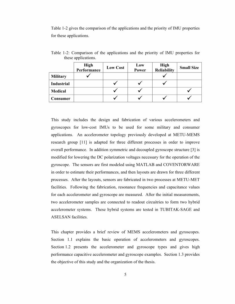
Table 1-2 gives the comparison of the applications and the priority of IMU properties
for these applications.
Table 1-2: Comparison of the applications and the priority of IMU properties for these applications.
High Performance Low Cost Low
Power High
Reliability Small Size
Military
Industrial
Medical Consumer
This study includes the design and fabrication of various accelerometers and
gyroscopes for low-cost IMUs to be used for some military and consumer
applications. An accelerometer topology previously developed at METU-MEMS
research group [11] is adapted for three different processes in order to improve
overall performance. In addition symmetric and decoupled gyroscope structure [3] is
modified for lowering the DC polarization voltages necessary for the operation of the
gyroscope. The sensors are first modeled using MATLAB and COVENTORWARE
in order to estimate their performances, and then layouts are drawn for three different
processes. After the layouts, sensors are fabricated in two processes at METU-MET
facilities. Following the fabrication, resonance frequencies and capacitance values
for each accelerometer and gyroscope are measured. After the initial measurements,
two accelerometer samples are connected to readout circuitries to form two hybrid
accelerometer systems. These hybrid systems are tested in TUBITAK-SAGE and
ASELSAN facilities.
This chapter provides a brief review of MEMS accelerometers and gyroscopes.
Section 1.1 explains the basic operation of accelerometers and gyroscopes.
Section 1.2 presents the accelerometer and gyroscope types and gives high
performance capacitive accelerometer and gyroscope examples. Section 1.3 provides
the objective of this study and the organization of the thesis.
6
1.1 Basic Operation Principles of Accelerometers and Gyroscopes
An accelerometer is a sensor that senses external acceleration. To extract the
acceleration value, the sensor has a movable proof mass which is connected to a
fixed frame via spring structures. When there is an external acceleration, the proof
mass is displaced from its rest position. The magnitude of this displacement is
proportional to the magnitude of the acceleration and inversely proportional to the
stiffness of the spring structures. Hence, the acceleration input that is applied to the
sensor is converted to the proof mass displacement in the sensor. The sensor then
extracts the magnitude of this displacement using its sensing scheme. The
accelerometers are characterized using their sensing schemes, and this
characterization is explained in the next section. A detailed operation principle of
the accelerometer is given in Chapter 2.
A gyroscope is a sensor that senses external angular velocity. The similarity of the
operation principle of the gyroscope with that of the accelerometer is that, the
gyroscope converts the angular velocity input to displacement of its proof mass. For
this purpose the gyroscope uses the Coriolis acceleration principle [1, 3, 6]. First the
proof mass of the gyroscope is vibrated in one axis, and then when there is an
external angular velocity, the proof mass starts vibrating in another axis due to
Coriolis acceleration principle. The second vibration magnitude is proportional to
the angular velocity input magnitude. Hence, the sensing scheme of the gyroscope
extracts the magnitude of the input angular velocity with extracting the magnitude of
the secondary vibration. A detailed operation principle of the gyroscope is also
provided in Chapter 2.
7
1.2 Classification of MEMS Accelerometers and Gyroscopes
MEMS accelerometers and gyroscopes can be mainly classified into eight groups
according to their sensing mechanisms:
• Capacitive
• Optical
• Piezoresistive
• Piezoelectric
• Thermal
• Tunneling current
• Resonant
• Magnetic
In capacitive accelerometers, the proof mass displacement is detected with the
change in the capacitance between the proof mass and the sense electrodes. In
capacitive gyroscopes, the primary vibration is obtained using electrostatic forces
between the proof mass and the drive electrodes, and the proof mass displacement
due to secondary vibration is detected with the charge in the capacitance between the
proof mass and the sense electrodes similar to that of the capacitive accelerometers.
Capacitive sensors have important advantages compared to other types of inertial
sensors. They have simple structure and hence low fabrication cost. In addition,
they provide low power consumption, high sensitivity, and high reliability as well as
low nonlinearity, low temperature dependency, low noise, and low drift. DRIE,
LIGA and other advanced MEMS processes enable the fabrication of very high
aspect ratio structures which improves the sensitivity of the sensors [18-20]. Using
DRIE and high performance capacitive readout circuits, 1 µg/√Hz resolution is
achieved in accelerometers [7], and 10.4°/hr/√Hz resolution is achieved for the
gyroscopes [18].
8
Capacitive sensors are widely preferred in consumer application due to their high
performance, reliability, and low cost. Analog Devices commercialized capacitive
accelerometers and also gyroscopes. ADXL series accelerometers available in the
market with different resolution and operation range choices. These sensors are
fabricated with surface micromachining with polysilicon as the structural layer
monolithically integrated with the readout electronics [21], and intended for
consumer applications. ADXRS series gyroscopes are also available in the market
for consumer applications.
Optical inertial sensors are rather difficult to fabricate but show high performances.
The major advantages for optical inertial sensors are that they are immune to
electromagnetic interference and they can operate at high temperatures. They show
high performances but fabrication of light emitting and sensing components using
micromachining techniques is not easy [11]. A 90 µg/√Hz resolution optic
accelerometer is reported in the literature [22]. For the gyroscopes, fiber-optic
gyroscopes are the first replacements of the big mechanical gyroscopes. However,
they have a more complex fabrication compared to capacitive MEMS gyroscopes.
Piezoresistive sensing scheme is widely used in accelerometers [23-25]. However, to
use piezoresistive materials in gyroscopes, the gyroscope should be driven in its
primary mode with a different mechanism due to the fact that piozoresistive
materials cannot induce force due to its passive nature [26]. Sensors using
piezoresistive materials are easy to fabricate and they have simple readout circuitries.
However, their sensitivity is low [6], and their temperature dependency is high [11]
compared to capacitive sensors. Therefore, they are not preferred for high
performance applications. In the literature, piezoresistive accelerometer with
0.2 mg/√Hz is reported [23]. There are also gyroscopes using different drive
mechanism such as piezoelectric or magnetic, and use piezoresistive sensing [27-28].
9
The operation of piezoelectric sensors requires an external stress similar to the
piezoresistive sensors. The sensitive material stores a charge on itself proportional to
this external stress. This charge-storage makes the sensor an active device,
theoretically providing it to generate its own power and provides low power sensor
design [11]. In addition to this, the fabrication of piezoelectric sensors is as easy as
piozoresistive sensors enabling low cost sensor realization. However, the main
disadvantage of the piezoelectric sensors is that they do not have a DC response due
to the fact that the charge stored on the piezoelectric material leaks away under a
constant stress [11]. Therefore, low frequency operation is not possible. This fact
makes it difficult to realize piezoelectric accelerometer since accelerometers are
generally used to sense low frequency accelerations. However for the gyroscopes,
the problem is not as critical as it for the accelerometers because the gyroscope
brings the input angular velocity input frequency to its drive mode resonance
frequency which is around a few kHz. Another disadvantage for the piezoelectric
sensors is the difficulty in readout electronics. The output resistance of the sensor is
high, hence it is difficult to get the signal out. There are piezoelectric accelerometer
examples in the literature [29-30] and also a commercial gyroscope example realized
by Murata Inc. [31].
There are also different sensing scheme studies for accelerometers such as thermal
sensing [32]. In this example the proof mass of the accelerometer is a hot air bubble
which is placed between two electrodes. When there is not any input acceleration, the
temperature difference between the electrodes is fixed. However, when an external
acceleration is applied, this bubble moves and changes the temperature difference
between the electrodes. Hence, the acceleration is converted to the temperature
difference. This temperature difference is sensed and acceleration is extracted.
Another type of accelerometer is resonant type accelerometer which directly finds
the applied force onto the proof mass [33]. The proof mass is vibrated in its natural
resonance frequency and the inertial force caused by external acceleration changes
the resonance frequency of the system. By finding the shift in the resonance
frequency, the magnitude of the acceleration can be extracted. A third type of
accelerometer is the tunneling current accelerometer, which has very low noise, has

10
wide bandwidth, and is highly sensitive. This type of accelerometer uses tunneling
current that occurs between two conductive layers located very close to each other.
The distance between these electrodes should be about 10 Å to create a tunneling
current [11]. When there is an external acceleration, one of the conductive layers
moves, and changes the tunneling current. With this reading scheme very low noise
levels like 20 ng/√Hz is achieved for accelerometers [34], but high drift values,
fabrication complexity, and high cost prevent tunneling accelerometers to be widely
used in the industry.
Magnetism is generally used to create the drive mode vibration of the gyroscopes
[35]. However, gyroscopes with electromagnetic drive and sensing schemes are also
reported [36]. But, the performance of these sensors is not as promising as the
capacitive ones.
In summary, there are a number of approaches to implement accelerometers and
gyroscopes, but the widely used one is the capacitive approach, as it is suitable for
MEMS fabrication techniques. Therefore, capacitive approach is used in this study
to implement various accelerometers and gyroscopes.
1.3 Objectives of the Study and the Organization of the Thesis
The objectives of this study can be summarized as below:
• The main objective of this study to construct an accelerometer system which
has satisfactory noise-floor/nonlinearity performance for IMUs to be used in
some military and consumer applications and is powered with only ±12 DC
batteries. The system is to yield a voltage output proportional to the
externally applied accelerometer. The proposed system is composed of a
MEMS accelerometer, a capacitive readout circuit, the bias circuitry for this
capacitive readout circuit, and amplifier stages. Table 1-3 summarizes the
performance goals of this hybrid accelerometer system. Sensitivity and
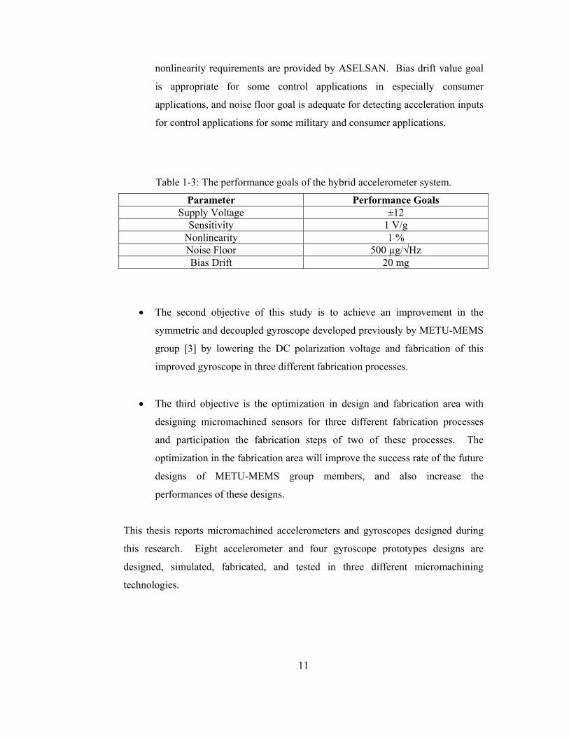
11
nonlinearity requirements are provided by ASELSAN. Bias drift value goal
is appropriate for some control applications in especially consumer
applications, and noise floor goal is adequate for detecting acceleration inputs
for control applications for some military and consumer applications.
Table 1-3: The performance goals of the hybrid accelerometer system.
Parameter Performance Goals Supply Voltage ±12
Sensitivity 1 V/g Nonlinearity 1 % Noise Floor 500 µg/√Hz Bias Drift 20 mg
• The second objective of this study is to achieve an improvement in the
symmetric and decoupled gyroscope developed previously by METU-MEMS
group [3] by lowering the DC polarization voltage and fabrication of this
improved gyroscope in three different fabrication processes.
• The third objective is the optimization in design and fabrication area with
designing micromachined sensors for three different fabrication processes
and participation the fabrication steps of two of these processes. The
optimization in the fabrication area will improve the success rate of the future
designs of METU-MEMS group members, and also increase the
performances of these designs.
This thesis reports micromachined accelerometers and gyroscopes designed during
this research. Eight accelerometer and four gyroscope prototypes designs are
designed, simulated, fabricated, and tested in three different micromachining
technologies.
12
Chapter 2 describes the theoretical background required for the design of MEMS
accelerometers and gyroscopes. Specifically, it explains some commonly used
mechanical definitions, spring constant derivation methods, Coriolis force definition,
and also accelerometer and gyroscope models.
Chapter 3 focuses the design and modeling of accelerometer and gyroscope
prototypes. First, it explains the important performance parameters for
accelerometers and gyroscopes. Next, it gives the design considerations for the
fabrication imperfections. Then, the chapter provides the details of accelerometer
and gyroscope designs with giving the topologies, MATLAB/COVENTORWARE
simulation results, and comparison of these results for these designs. Finally the
chapter gives the expected performance values of the designed sensors.
Chapter 4 gives the details of the three fabrication processes that are used to
implement the accelerometers and the gyroscopes in this study. The first process is
called SOIMUMPs and it is performed by a commercial MEMS foundry. The
second process is based on electroplating process developed by METU-MEMS
group. And the third process is based on DRIE etching. This process is currently
being developed at METU-MET for high performance accelerometers and
gyroscopes.
Chapter 5 provides the fabrication and test results. First, Scanning Electron
Microscope (SEM) and optical microscope pictures of the fabricated structures are
presented. Then, the chapter explains the tests performed on the accelerometer and
gyroscope samples. Next, it explains the hybrid accelerometer systems that are
constructed by connecting high performance SOIMUMPs and nickel electroplated
accelerometer samples to the commercially available MS3110 readout circuit.
Finally, the chapter gives the test results that are done to characterize the hybrid
systems.
Finally, Chapter 6 gives the conclusion of the thesis and suggests future studies to
improve MEMS accelerometer and gyroscope systems.
13
CHAPTER 2
THEORETICAL BACKGROUND
This chapter presents the theoretical background on the design of capacitive MEMS
accelerometers and gyroscopes. Section 2.1 gives the definitions of some commonly
used mechanical terms related with the accelerometer and gyroscope design. Section
2.2 explains the derivation of spring constants for variable spring shapes. Section 2.3
discusses the Coriolis force, which causes the secondary motion in the vibratory
gyroscopes. Section 2.4 explains the basic accelerometer and gyroscope model.
Section 2.5 explains different capacitive sensing and actuating topologies used in
accelerometers and gyroscopes. Finally, Section 2.6 gives the summary of the whole
chapter.
2.1 Definitions of Some Commonly Used Mechanical Terms
The design of accelerometers or gyroscopes needs strong background in both
electrical and mechanical area. For the mechanical side, the designer should be
familiar with some common mechanical terms like stress, strain, elasticity [3]. In
this section, the definitions of these terms are given. Some mechanical terms like
Poisson’s ratio are also mentioned for the sake of completeness although it is not
directly related with the mechanical design.
14
Stress is the defined as the force per unit area acting on the surface of a differential
volume element of a solid body [26]. The stresses that are caused by forces
perpendicular to differential face is called normal stresses and the stress caused by
forces along the face is called shear stresses [26]. Normal stress is generally denoted
by σ, and shear stress is generally denoted by τ. Equation 2.1 shows the basic
formulation of stress where F is the applied force and A is the cross sectional area
[37].
AF
=σ (N/m2) (2.1)
The stress can either be compressive or tensile depending on the direction of the
force acting on the differential face [38]. This fact is mostly important in fabrication
issues whether the fabricated structure will deform or not after a release operation.
Another important mechanical term is the Strain, which can be defined as the
deformation resulting from a stress, and measured as the ratio of deformation to the
total dimension of the body in which the deformation is occurred. The deformation
depends on the direction of the applied force. The compressive force causes the
body to be shortened and the tensile force causes the body to be stretched [3]. The
normal strain is denoted by ε and formulated as:
Lδε = (2.2)
where δ is the amount of deformation and L is the original dimension. Shear strain is
denoted by γ.
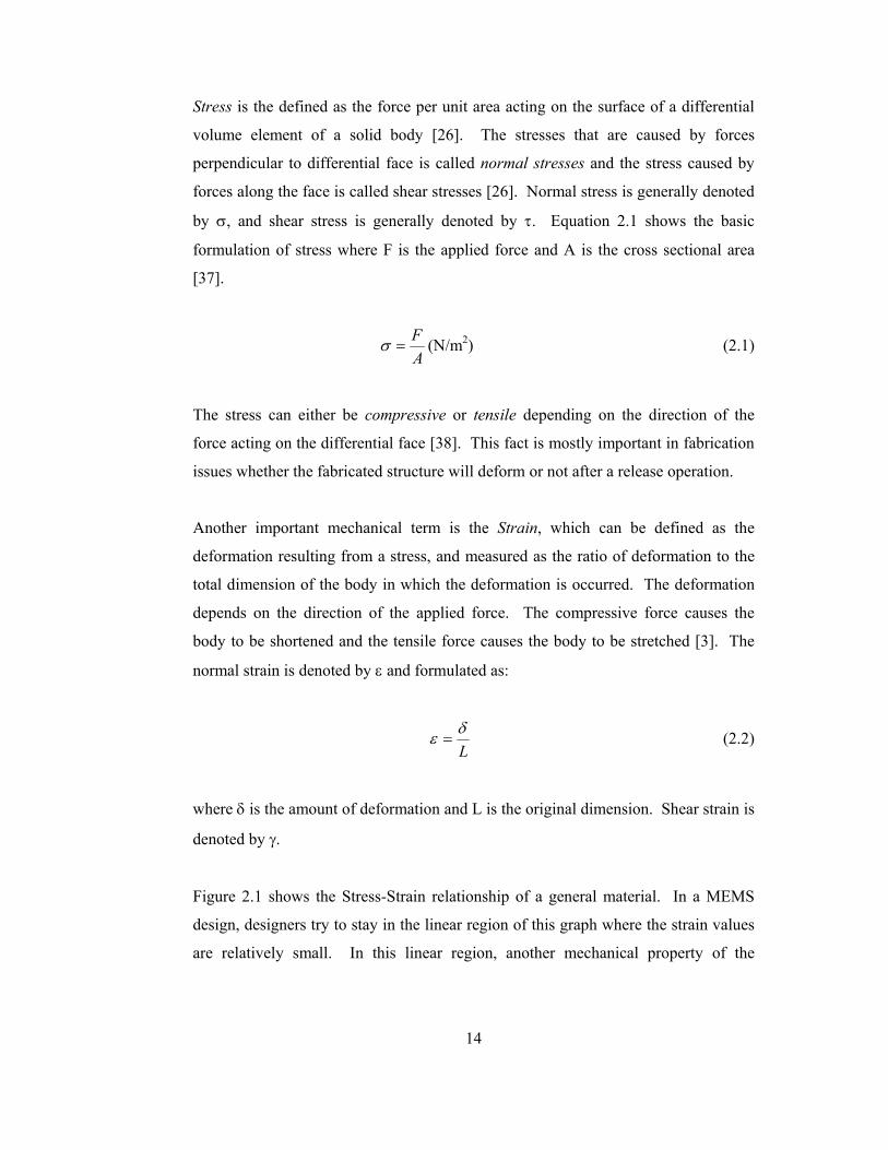
Figure 2.1 shows the Stress-Strain relationship of a general material. In a MEMS
design, designers try to stay in the linear region of this graph where the strain values
are relatively small. In this linear region, another mechanical property of the
15
materials can be defined as Young’s Modulus which is the proportionality constant in
this linear region and can be expressed as:
εσ
=E (N/m2) (2.3)
where E denotes Young’s Modulus [37].
Brittle fractureYield
Strain
Stre
ss
Elastomeric or Flow Region
Hardening
Ductile Fracture
Figure 2.1: Stress-Strain relationship of a general material [26].
In real life, if there is deformation in one direction due to a stress source, there will
be deformations in other directions. If a beam is squeezed so that its length is
shortened, than the width of the beam widens. From this fact, another mechanical
term is defined. Poisson’s Ratio is the ratio of lateral strain to axial strain and is
generally denoted by ν [37].
16
Moment of Inertia is also an important term in MEMS design. Moment of inertia of
an area with respect to an axis is the sum of the products obtained by multiplying the
infinitesimal area elements by the distance of this element from the axis. Moment of
inertia is denoted by ‘I’ and can be expressed as:
dAyI ∫= 2 (2.4)
where dA is the infinitesimal area element and y is the distance of this area element
to the origin of interest.
2.2 Derivation of Spring Constant for Variable Spring Shapes
In MEMS accelerometers and gyroscopes, spring constants play an important role in
determining the performances of the sensors. The performance of the sensors is
related with the easiness in the movement of the proof mass in certain directions and
also with the difficulty in the movement of the proof mass in some other directions.
Hence, determining the spring constants in all directions is an important design step.
In this chapter, spring constant calculations in each three directions will be discussed.
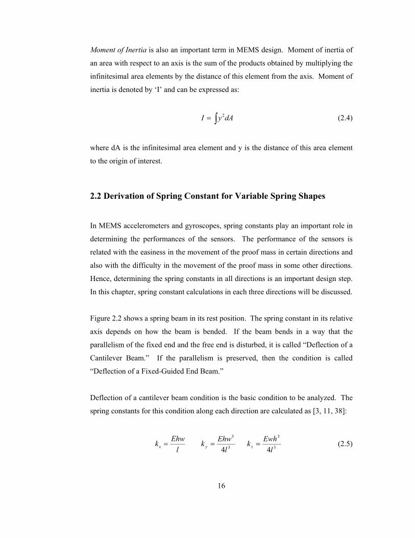
Figure 2.2 shows a spring beam in its rest position. The spring constant in its relative
axis depends on how the beam is bended. If the beam bends in a way that the
parallelism of the fixed end and the free end is disturbed, it is called “Deflection of a
Cantilever Beam.” If the parallelism is preserved, then the condition is called
“Deflection of a Fixed-Guided End Beam.”
Deflection of a cantilever beam condition is the basic condition to be analyzed. The
spring constants for this condition along each direction are calculated as [3, 11, 38]:
lEhwkx = 3
3
4lEhwk y = 3
3
4lEwhkz = (2.5)
17
where the direction index denotes the direction of the applied force which bends the
spring beam, E is the Young’s Modulus, h is the thickness, w is the width, and l is
the length of the beam.
h
w
l Anchor
x
y
z
Figure 2.2: A spring beam in its rest position.
The spring constant for fixed-guided end beam can be found by using the deflection
formulation similar to the cantilever beam condition [38]. Another way of
calculating the spring constant of fixed-guided end beam is to use parallel and series
spring constants. Figure 2.3 shows the resultant spring constant of parallel and series
connected springs.
Fixed-guided end beam deflection can be modeled as series connected of two half
length clamped beam springs. Figure 2.4 shows the series connection of two half
length clamped beam springs forming a fixed-guided end beam. From this
observation, the spring constant for a fixed-guided beam can be found as:
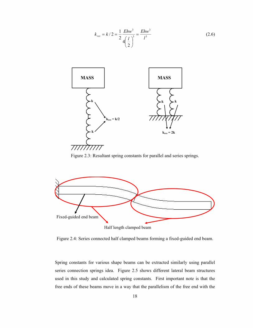
18
3
3
3
3
24
212/
lEhw
lEhwkkres =
== (2.6)
MASS MASS
k
k
k k
kres = k/2
kres = 2k
Figure 2.3: Resultant spring constants for parallel and series springs.
Half length clamped beam
Fixed-guided end beam
Figure 2.4: Series connected half clamped beams forming a fixed-guided end beam.
Spring constants for various shape beams can be extracted similarly using parallel
series connection springs idea. Figure 2.5 shows different lateral beam structures
used in this study and calculated spring constants. First important note is that the
free ends of these beams move in a way that the parallelism of the free end with the
19
fixed end is preserved. This can be achieved by symmetrical beam allocations
around the proof mass. Another important note is the rigidity of the truss regions. If
the truss regions remain rigid when the beam deflects, we assume that all the sub-
beams forming the total beam are fixed-guided end beams keeping in mind that first
note condition is preserved. In this study, the truss region widths are designed to be
at least 4 times wider then the beam widths to preserve the rigidity of the truss
regions. In addition the beams are allocated symmetrically around the proof mass
not to disturb the parallelism of the free and fixed end of the beams.
Although the spring constant calculations for lateral beams can model the real beams
with a good accuracy, we cannot achieve a similar accuracy in z-axis beams. The
reason behind this fact is the rotation of the truss regions. While the beams in Figure
2.5 are deflected in z-axis, the truss regions tend to rotate although the rigidity is
preserved. Thus, the sub-beams have additional rotational spring constants. Due to
this fact, it is better to design the z-axis beams using FEM simulators or more
sophisticated spring constant extraction programs.
3
3
LEhwk =
L
w
y
x z
L
Truss region
kres = k/2
kres = 2(k/2) = k
Free end
Figure 2.5: Different spring structures used in this study and calculated resultant
spring constants.
20
2.3 Coriolis Force
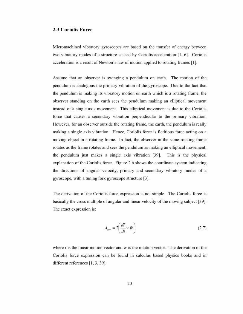
Micromachined vibratory gyroscopes are based on the transfer of energy between
two vibratory modes of a structure caused by Coriolis acceleration [1, 6]. Coriolis
acceleration is a result of Newton’s law of motion applied to rotating frames [1].
Assume that an observer is swinging a pendulum on earth. The motion of the
pendulum is analogous the primary vibration of the gyroscope. Due to the fact that
the pendulum is making its vibratory motion on earth which is a rotating frame, the
observer standing on the earth sees the pendulum making an elliptical movement
instead of a single axis movement. This elliptical movement is due to the Coriolis
force that causes a secondary vibration perpendicular to the primary vibration.
However, for an observer outside the rotating frame, the earth, the pendulum is really
making a single axis vibration. Hence, Coriolis force is fictitious force acting on a
moving object in a rotating frame. In fact, the observer in the same rotating frame
rotates as the frame rotates and sees the pendulum as making an elliptical movement;
the pendulum just makes a single axis vibration [39]. This is the physical
explanation of the Coriolis force. Figure 2.6 shows the coordinate system indicating
the directions of angular velocity, primary and secondary vibratory modes of a
gyroscope, with a tuning fork gyroscope structure [3].
The derivation of the Coriolis force expression is not simple. The Coriolis force is
basically the cross multiple of angular and linear velocity of the moving subject [39].
The exact expression is:
×= w
dtrdAcor
rr
2 (2.7)
where r is the linear motion vector and w is the rotation vector. The derivation of the
Coriolis force expression can be found in calculus based physics books and in
different references [1, 3, 39].
21
Secondary mode
Primary Mode
Rotation
Rotation
Primary Primary
Secondary
Secondary
Figure 2.6: Coordinate system showing primary and secondary modes of a gyroscope
with a tuning fork gyroscope structure [3].
2.4 Accelerometer and Gyroscope Models
This chapter explains the basic accelerometer and gyroscope models. The
accelerometer can be modeled as a mass-spring-damper system where an external
acceleration causes the proof mass to deflect from its rest position. The gyroscope
can be modeled as a Coriolis acceleration sensing accelerometer. In the gyroscopes,
there is a primary mode vibrator to create Coriolis acceleration under an external
rotation.
2.4.1 Accelerometer Model
Figure 2.7 shows a general mass-spring-damper system. When there is an external
acceleration the proof mass tends to move in the opposite direction of the
acceleration due to Newton’s law of motion. The proof mass movement is
22
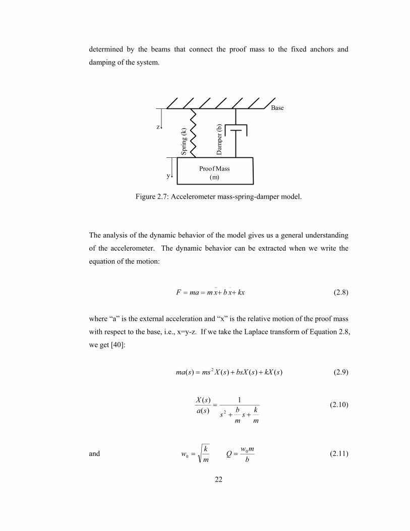
determined by the beams that connect the proof mass to the fixed anchors and
damping of the system.
Proof Mass(m) y
z
Sprin
g (k
)
Dam
per (
b)
Base
Figure 2.7: Accelerometer mass-spring-damper model.
The analysis of the dynamic behavior of the model gives us a general understanding
of the accelerometer. The dynamic behavior can be extracted when we write the
equation of the motion:
kxxbxmmaF ++==...
(2.8)
where “a” is the external acceleration and “x” is the relative motion of the proof mass
with respect to the base, i.e., x=y-z. If we take the Laplace transform of Equation 2.8,
we get [40]:
)()()()( 2 skXsbsXsXmssma ++= (2.9)
mks
mbssa
sX
++=
2
1)()( (2.10)
and mkw =0
bmw
Q 0= (2.11)
23
where w0 is the resonance frequency of the accelerometer and Q is the quality factor.
The magnitude and phase response of the proof mass motion with respect to input
acceleration can be derived as:
202220 )()(
1)()(
Qww
wwjwajwX
+−
= (2.12)
)(tan)()(
220
0
1
wwQ
ww
jwajwX
−=∠ − (2.13)
Figure 2.8 shows the plot of the magnitude of proof mass displacement under a
constant magnitude external acceleration versus acceleration frequency. The
accelerometer is operated in the linear region of this plot due to the fact that the
response is almost constant. The magnitude of the response in this linear region is
inversely proportional to the square of the resonance frequency of the accelerometer.
Hence, the mechanical resonance frequency is a very important parameter
determining the performance of the accelerometer. The length of this linear region is
called the effective bandwidth of the accelerometer. The effective bandwidth is also
an important design parameter, and it is mainly related to the resonance frequency of
the accelerometer. It should also be noted that, the definition of the effective
bandwidth requires a better explanation of the length of the linear region. The linear
region is not perfectly linear, but it shows a small response error. Figure 2.9 shows
the focused view of this linear response region and indicates the response error. The
effective bandwidth of the accelerometer is a design goal and the designer should
design the accelerometer properly to achieve reasonably small response errors in that
bandwidth.
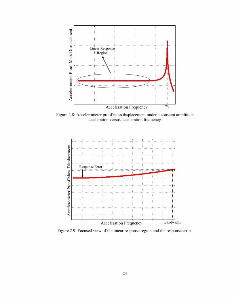
24
Acceleration Frequency
Acc
eler
omet
erPr
oofM
assD
ispl
acem
ent
w0
Linear Response Region
Figure 2.8: Accelerometer proof mass displacement under a constant amplitude
acceleration versus acceleration frequency.
Acceleration Frequency
Acc
eler
omet
erPr
oofM
assD
ispl
acem
ent
Response Error
Bandwidth Figure 2.9: Focused view of the linear response region and the response error.
25
The effective bandwidth of the accelerometer or the response error in a predefined
bandwidth is related to the resonance frequency and the quality factor of the system.
Table 2-1 shows the response error of the accelerometer for 100 Hz effective
bandwidth under different resonance frequency and quality factor values. The first
observation according to the data provided in Table 2-1 is that when the frequency of
the accelerometer increases for a fixed quality factor value, the response error
decreases. Hence, to achieve a wider effective bandwidth, one can choose a higher
resonance frequency. But, the resonance frequency of the accelerometer should be
as low as possible to get a higher response values in that linear range because the
proof mass displacement in that linear range is:
20waX = (m) (2.14)
Hence, to find an optimum value between resonance frequency and the effective
bandwidth is an important design issue. The second observation is, when the quality
factor is 0.7, which means that the system is critically damped, very small response
errors can be achieved with very small resonance frequencies [1, 41]. However,
when the quality factor is changed slightly from 0.7, the response error is increased
rapidly. The last important observation is the effect of higher quality factor values to
response error. When the quality factor value is larger than 2, the response error for
different resonance frequencies do not change significantly. To sum up above
observations, to achieve a small response error in a fixed effective bandwidth, the
design of the accelerometer can be done in two different ways. First way is to fix the
quality factor at 0.7 and then to use a very small resonance frequency. This can be
achieved with close loop configuration. The second way is to use a higher quality
factor and to set resonance frequency 20-25 times more than the required effective
bandwidth.

26
Table 2-1: Response error of the accelerometer for 100 Hz accelerometer effective bandwidth.
Accelerometer Effective
Bandwidth (Hz) Quality Factor Resonance
Frequency (Hz) Response Error
(%)
100 0.5 500 4.00 100 0.5 2000 0.24 100 0.7 500 0.18 100 0.7 750 0.06 100 2 750 1.58 100 2 2000 0.23 100 2 2500 0.15 100 5 2000 0.26 100 5 2500 0.15 100 100 2000 0.26 100 100 2500 0.15 100 1000 2000 0.26 100 1000 2500 0.15
In the quality factor expression given in Equation 2.11, the parameter that the
designer has the least control is the damping factor, “b”. The damping factor value
of the accelerometer system depends on mainly air, structural, and thermal effects.
The air damping results from the internal friction of the moving gas in small
clearances between moving elements [42]. There are two main air damping effects
namely “Squeeze-film damping”, and “Coutte-flow damping”. In Squeeze-damping
effect, the air molecules are squeezed between two plates that are relatively moving
towards each other. In Coutte-flow damping, the friction is occurred between two
plates that are relatively moving parallel to each other. These to damping effects can
be modeled and mathematical expressions can be obtained [43-44]. But these
equations are obtained using some assumptions like having very large plates, hence
they cannot hold in finger or etch hole regions of the MEMS sensors. Some
sophisticated models for a better approach in solving this problem can be found in
the literature [45-46]. However, the exact air damping calculation for specific device
geometry is nearly impossible without using a FEM solver. Although an FEM solver
can give some values for air damping, we cannot say the similar thing for structural
damping. The structural damping is due to the energy loss in the structure of the
MEMS device. The value of this damping is highly process dependent because even
27
the stiction of the anchor regions to the substrate is a source of this damping. The
final main damping effect is the thermal damping. The main reason for this effect is
the deviation of stress-strain relation with changing temperature [47]. It is very
difficult for the designer to achieve a certain quality factor value due to the fact that
each damping factor value extracted from the above sources is not accurate enough.
However, this uncertainty in the quality factor may not be a disadvantage for the
designer if he aims a quality factor value different than 0.7. From the observations
that are derived from Table 2-1, we already know that the quality factor value more
than 2 does not affect the response error significantly. Moreover, quality factor
values smaller than 0.7 also gives similar response errors with quality factor values
larger than 0.7. Hence, if the quality factor turns out to be different from what is
expected in the design period, the performance of the accelerometer is not affected
significantly.
The best way to achieve 0.7 quality factor is to use closed loop system [1]. In closed
loop accelerometer, the proof mass is kept in its rest position using a feedback
voltage proportional to the external acceleration [26]. Hence, the effects of air
damping are removed due to the fact that the proof mass movement is negligibly
small. So, the peak in the response plot of the accelerometer is suppressed, providing
a large linear range. However, there is a major disadvantage of the close loop system,
which is the complexity of the readout circuit. Although the highest performance
values for accelerometers are achieved with close loop topology [7, 48], the
accelerometers in this study are designed for open loop system because of the
complex readout circuitry problem of the close loop systems.
2.4.2. Gyroscope Model
Figure 2.10 shows the general structure of a gyroscope. Gyroscopes are angular rate
sensors, and for this purpose they use Coriolis acceleration. Due to this fact a
gyroscope should have a vibratory motion generator which is needed for the
generation of the Coriolis force which we call drive mode or primary mode of the
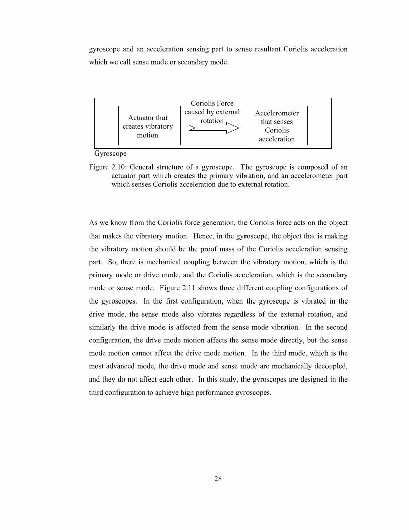
28
gyroscope and an acceleration sensing part to sense resultant Coriolis acceleration
which we call sense mode or secondary mode.
Actuator that creates vibratory
motion
Accelerometer that senses
Coriolis acceleration
Coriolis Force caused by external
rotation
Gyroscope Figure 2.10: General structure of a gyroscope. The gyroscope is composed of an
actuator part which creates the primary vibration, and an accelerometer part which senses Coriolis acceleration due to external rotation.
As we know from the Coriolis force generation, the Coriolis force acts on the object
that makes the vibratory motion. Hence, in the gyroscope, the object that is making
the vibratory motion should be the proof mass of the Coriolis acceleration sensing
part. So, there is mechanical coupling between the vibratory motion, which is the
primary mode or drive mode, and the Coriolis acceleration, which is the secondary
mode or sense mode. Figure 2.11 shows three different coupling configurations of
the gyroscopes. In the first configuration, when the gyroscope is vibrated in the
drive mode, the sense mode also vibrates regardless of the external rotation, and
similarly the drive mode is affected from the sense mode vibration. In the second
configuration, the drive mode motion affects the sense mode directly, but the sense
mode motion cannot affect the drive mode motion. In the third mode, which is the
most advanced mode, the drive mode and sense mode are mechanically decoupled,
and they do not affect each other. In this study, the gyroscopes are designed in the
third configuration to achieve high performance gyroscopes.
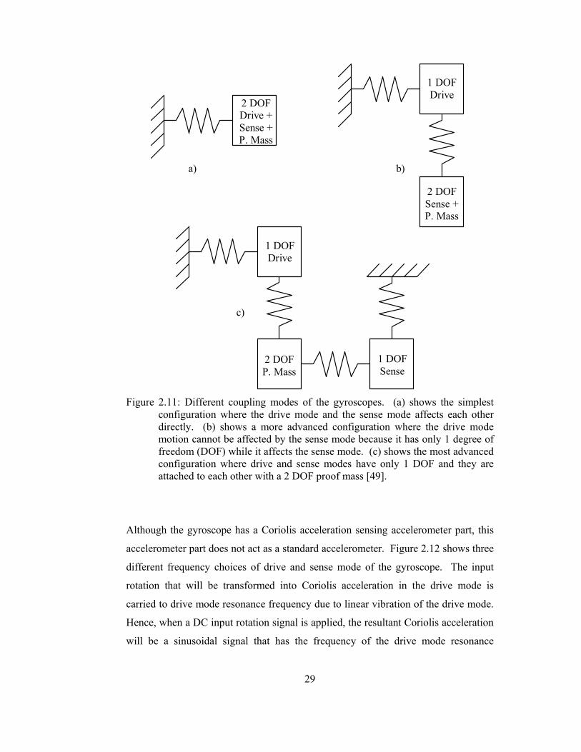
29
a) b)
c)
2 DOF Drive + Sense + P. Mass
1 DOF Drive
2 DOF Sense + P. Mass
1 DOF Drive
1 DOF Sense
2 DOF P. Mass
Figure 2.11: Different coupling modes of the gyroscopes. (a) shows the simplest
configuration where the drive mode and the sense mode affects each other directly. (b) shows a more advanced configuration where the drive mode motion cannot be affected by the sense mode because it has only 1 degree of freedom (DOF) while it affects the sense mode. (c) shows the most advanced configuration where drive and sense modes have only 1 DOF and they are attached to each other with a 2 DOF proof mass [49].
Although the gyroscope has a Coriolis acceleration sensing accelerometer part, this
accelerometer part does not act as a standard accelerometer. Figure 2.12 shows three
different frequency choices of drive and sense mode of the gyroscope. The input
rotation that will be transformed into Coriolis acceleration in the drive mode is
carried to drive mode resonance frequency due to linear vibration of the drive mode.
Hence, when a DC input rotation signal is applied, the resultant Coriolis acceleration
will be a sinusoidal signal that has the frequency of the drive mode resonance
30
frequency. Similarly, when a timely varying input rotation signal is applied, the
Coriolis acceleration frequency will be shifted according to the frequency of this
input rotation. Hence, the sense mode should be capable of detecting acceleration
inputs with the frequencies in the required bandwidth of the drive mode resonance
frequency. In the part (a) of Figure 2.12 the resonance frequency of the sense mode
is very large to achieve linear response for different Coriolis acceleration frequencies.
From the accelerometer bandwidth-linear response observations, it is concluded that
the sense mode resonance frequency of the gyroscope should be 20-25 times more
than the drive mode resonance frequency to have a linear response. But, this will be
a very inefficient solution because the signal levels at the output of the sense mode
will be very low due to very high resonance frequency of the sense mode considering
that the drive mode resonance frequencies of the gyroscopes are around few kHz. In
the part (b) of Figure 2.12 the resonance frequencies of the drive mode and the sense
mode of the gyroscope are designed to be mismatched, but their difference is not big
as part (a). The response error is compensated with external electronics which is
sensitive to Coriolis acceleration frequency. In the part (c) of Figure 2.12, the
resonance frequencies of the drive and sense mode are designed to be matched. In
this case, the magnitude of the Coriolis acceleration is multiplied with the quality
factor of the system and so is very large compared to part (b) but 3dB bandwidth of
the system is decreased. The response error is compensated with external electronics
similarly.
In this study, the gyroscopes are designed to have matched resonance frequencies.
But, due to fabrication errors that cannot be avoided, the gyroscopes will have
slightly mismatched resonance frequencies [39]. So, in the gyroscope designs, there
are also some control electrodes that can compensate this frequency mismatch. In
the designs, there are also some electrodes that are put to cancel quadrature error
which is due to misalignment of the drive mode axis with respect to sense mode axis
[50-51].
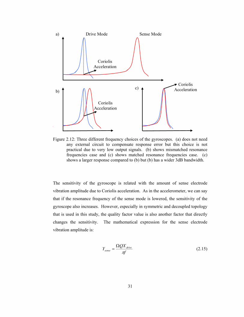
31
Sense Mode Drive Mode
Coriolis Acceleration
Coriolis Acceleration
Coriolis Acceleration
a)
b) c)
Figure 2.12: Three different frequency choices of the gyroscopes. (a) does not need
any external circuit to compensate response error but this choice is not practical due to very low output signals. (b) shows mismatched resonance frequencies case and (c) shows matched resonance frequencies case. (c) shows a larger response compared to (b) but (b) has a wider 3dB bandwidth.
The sensitivity of the gyroscope is related with the amount of sense electrode
vibration amplitude due to Coriolis acceleration. As in the accelerometer, we can say
that if the resonance frequency of the sense mode is lowered, the sensitivity of the
gyroscope also increases. However, especially in symmetric and decoupled topology
that is used in this study, the quality factor value is also another factor that directly
changes the sensitivity. The mathematical expression for the sense electrode
vibration amplitude is:
fQX
Y drivesense π
Ω= (2.15)
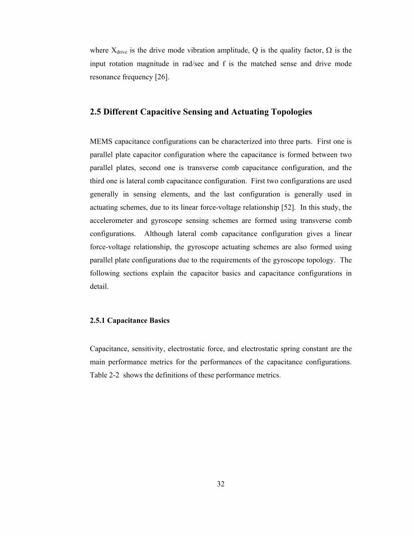
32
where Xdrive is the drive mode vibration amplitude, Q is the quality factor, Ω is the
input rotation magnitude in rad/sec and f is the matched sense and drive mode
resonance frequency [26].
2.5 Different Capacitive Sensing and Actuating Topologies
MEMS capacitance configurations can be characterized into three parts. First one is
parallel plate capacitor configuration where the capacitance is formed between two
parallel plates, second one is transverse comb capacitance configuration, and the
third one is lateral comb capacitance configuration. First two configurations are used
generally in sensing elements, and the last configuration is generally used in
actuating schemes, due to its linear force-voltage relationship [52]. In this study, the
accelerometer and gyroscope sensing schemes are formed using transverse comb
configurations. Although lateral comb capacitance configuration gives a linear
force-voltage relationship, the gyroscope actuating schemes are also formed using
parallel plate configurations due to the requirements of the gyroscope topology. The
following sections explain the capacitor basics and capacitance configurations in
detail.
2.5.1 Capacitance Basics
Capacitance, sensitivity, electrostatic force, and electrostatic spring constant are the
main performance metrics for the performances of the capacitance configurations.
Table 2-2 shows the definitions of these performance metrics.
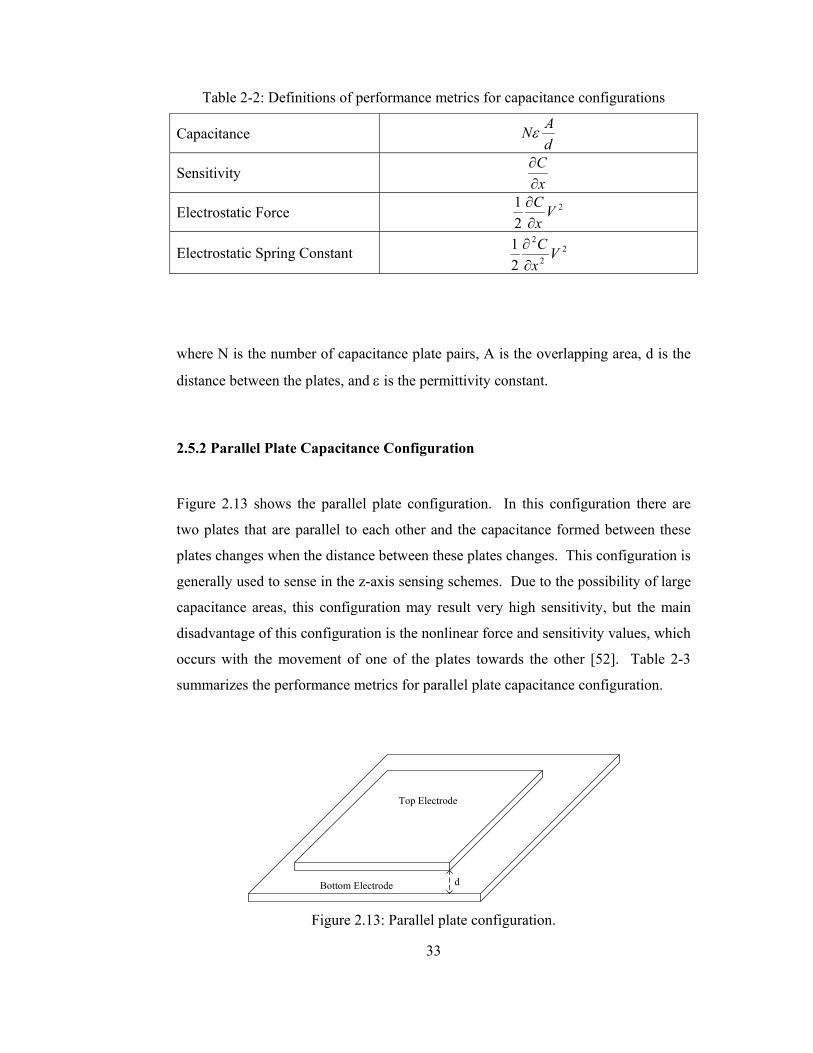
33
Table 2-2: Definitions of performance metrics for capacitance configurations
Capacitance dANε
Sensitivity xC∂∂
Electrostatic Force 2
21 V
xC∂∂
Electrostatic Spring Constant 22
2
21 V
xC
∂∂
where N is the number of capacitance plate pairs, A is the overlapping area, d is the
distance between the plates, and ε is the permittivity constant.
2.5.2 Parallel Plate Capacitance Configuration
Figure 2.13 shows the parallel plate configuration. In this configuration there are
two plates that are parallel to each other and the capacitance formed between these
plates changes when the distance between these plates changes. This configuration is
generally used to sense in the z-axis sensing schemes. Due to the possibility of large
capacitance areas, this configuration may result very high sensitivity, but the main
disadvantage of this configuration is the nonlinear force and sensitivity values, which
occurs with the movement of one of the plates towards the other [52]. Table 2-3
summarizes the performance metrics for parallel plate capacitance configuration.
d
Top Electrode
Bottom Electrode
Figure 2.13: Parallel plate configuration.
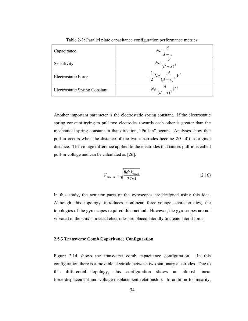
34
Table 2-3: Parallel plate capacitance configuration performance metrics.
Capacitance xd
AN−
ε
Sensitivity 2)( xdAN−
− ε
Electrostatic Force 22)(2
1 Vxd
AN−
− ε
Electrostatic Spring Constant 23)(
Vxd
AN−
ε
Another important parameter is the electrostatic spring constant. If the electrostatic
spring constant trying to pull two electrodes towards each other is greater than the
mechanical spring constant in that direction, “Pull-in” occurs. Analyses show that
pull-in occurs when the distance of the two electrodes become 2/3 of the original
distance. The voltage difference applied to the electrodes that causes pull-in is called
pull-in voltage and can be calculated as [26]:
Akd
V mechinpull ε27
8 3
=− (2.16)
In this study, the actuator parts of the gyroscopes are designed using this idea.
Although this topology introduces nonlinear force-voltage characteristics, the
topologies of the gyroscopes required this method. However, the gyroscopes are not
vibrated in the z-axis; instead electrodes are placed laterally to create lateral force.
2.5.3 Transverse Comb Capacitance Configuration
Figure 2.14 shows the transverse comb capacitance configuration. In this
configuration there is a movable electrode between two stationary electrodes. Due to
this differential topology, this configuration shows an almost linear
force-displacement and voltage-displacement relationship. In addition to linearity,
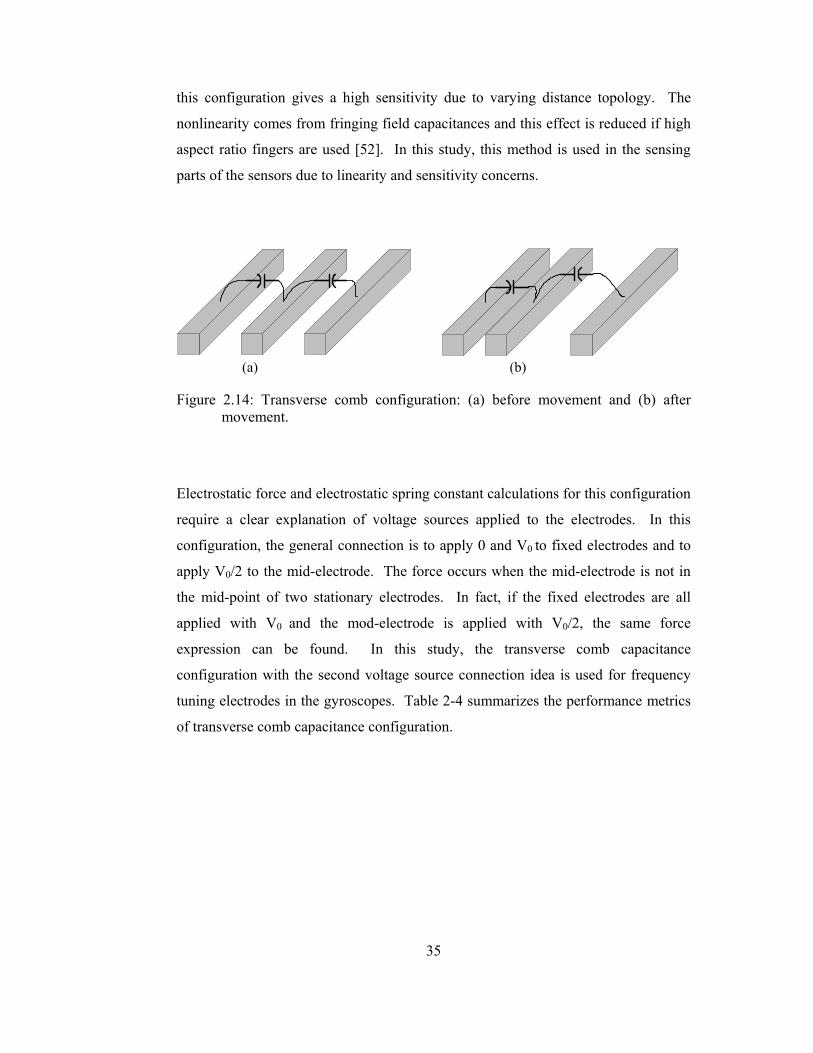
35
this configuration gives a high sensitivity due to varying distance topology. The
nonlinearity comes from fringing field capacitances and this effect is reduced if high
aspect ratio fingers are used [52]. In this study, this method is used in the sensing
parts of the sensors due to linearity and sensitivity concerns.
(a) (b)
Figure 2.14: Transverse comb configuration: (a) before movement and (b) after movement.
Electrostatic force and electrostatic spring constant calculations for this configuration
require a clear explanation of voltage sources applied to the electrodes. In this
configuration, the general connection is to apply 0 and V0 to fixed electrodes and to
apply V0/2 to the mid-electrode. The force occurs when the mid-electrode is not in
the mid-point of two stationary electrodes. In fact, if the fixed electrodes are all
applied with V0 and the mod-electrode is applied with V0/2, the same force
expression can be found. In this study, the transverse comb capacitance
configuration with the second voltage source connection idea is used for frequency
tuning electrodes in the gyroscopes. Table 2-4 summarizes the performance metrics
of transverse comb capacitance configuration.
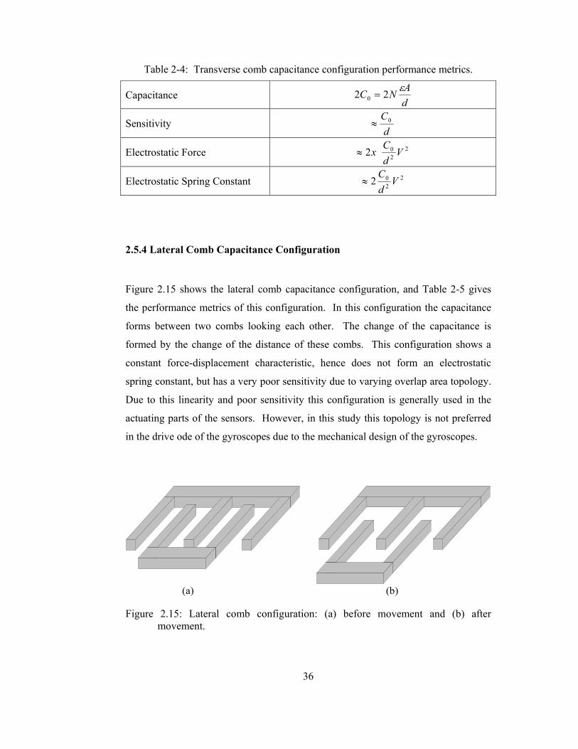
36
Table 2-4: Transverse comb capacitance configuration performance metrics.
Capacitance dANC ε22 0 =
Sensitivity d
C0≈
Electrostatic Force 2202 V
dC
x≈
Electrostatic Spring Constant 2202 V
dC
≈
2.5.4 Lateral Comb Capacitance Configuration
Figure 2.15 shows the lateral comb capacitance configuration, and Table 2-5 gives
the performance metrics of this configuration. In this configuration the capacitance
forms between two combs looking each other. The change of the capacitance is
formed by the change of the distance of these combs. This configuration shows a
constant force-displacement characteristic, hence does not form an electrostatic
spring constant, but has a very poor sensitivity due to varying overlap area topology.
Due to this linearity and poor sensitivity this configuration is generally used in the
actuating parts of the sensors. However, in this study this topology is not preferred
in the drive ode of the gyroscopes due to the mechanical design of the gyroscopes.
(a) (b)
Figure 2.15: Lateral comb configuration: (a) before movement and (b) after movement.
37
Table 2-5: Lateral comb capacitance configuration performance metrics.
Capacitance dAN ε
Sensitivity dhN ε
Electrostatic Force 2VdhN ε
Electrostatic Spring Constant 0
2.6 Summary
This chapter presents the theoretical background on the design of MEMS capacitive
accelerometers and gyroscopes. The basic mechanical terms are introduced and
Coriolis force concept is discussed. The models for accelerometers and gyroscopes
are given, and some design parameters such as quality factor and bandwidth is
studied. Lastly, the capacitive reading and actuating topologies are investigated for
different performance indicators.
38
CHAPTER 3
MEMS ACCELEROMETERS AND GYROSCOPES
DESIGN
This chapter gives the design details of MEMS accelerometers and gyroscopes.
Section 3.1 gives the important parameters that are considered as the design
challenges of the accelerometers, and Section 3.2 explains the important design
parameters and challenges for gyroscopes. Section 3.3 gives the details of designed
accelerometers and gyroscopes for three different processes with their estimated
performances. Finally, Section 3.4 gives the summary of this chapter.
3.1 Design Parameters and Challenges for MEMS Accelerometers
The most common MEMS accelerometer design parameters are resolution,
sensitivity (scale-factor), bandwidth, nonlinearity, bias drift, and scale factor
asymmetry. To achieve the required design parameters, the first thing the designer
should do is to choose a proper process. The process limitations directly affect the
performance of the sensors. Moreover, some parameters like nonlinearity, bias drift
and scale factor asymmetry cannot be estimated theoretically, because they are
almost totally process dependent. Hence, the choice of the process is an important
design issue. After choosing the process, the performance of the accelerometer can
39
be optimized with a proper mechanical design and with using a proper readout circuit.
The design parameters of MEMS accelerometers are shortly explained below.
Resolution is defined as the noise floor of the accelerometer system. The noise
sources in accelerometer system come from both mechanical and electrical parts of
the system. The mechanical noise source is the Brownian noise [53], and is related
with the mass and quality factor of the accelerometer mechanical part [26]. The
electrical noise source is the readout electronics electronic noise. In today’s
accelerometers, due to high proof mass values, the mechanical noise floor is nearly
neglected compared to electrical noise, but with a proper electrical circuitry design,
electrical noise floor can be reduced significantly [7]. The unit of the resolution
is g/√Hz or g in a fixed bandwidth where g is the earth gravity.
Sensitivity or scale-factor is the change in the response of the system to 1g
acceleration. The unit of sensitivity can be F/g if the mechanical part sensitivity is
considered only or V/g if mechanical part and readout circuitry is considered
together. The voltage sensitivity is not an indicator of the performance of the
accelerometer because with external amplifiers this sensitivity value can be arranged
to any value. However, the capacitance sensitivity mainly shows the performance of
the accelerometer mechanical part.
Bandwidth is the length of the frequency range that input signal frequency can vary.
While calculating the bandwidth of the accelerometer 3dB concept may not be used.
Instead, the maximum accelerometer response deviation with input acceleration
frequency change defines the bandwidth of the system. The bandwidth vales are
directly related to resonance frequency of the accelerometer.
Nonlinearity of the accelerometer is defined as the deviation of the accelerometer
response from the best fit curve for different magnitudes of acceleration signal in its
working range. Although the capacitive sensing topology may introduce nonlinearity,
especially parallel plate capacitive sensing topology, this nonlinearity is almost
insignificant compared to nonlinearity due to fabrication. The fabrication of the
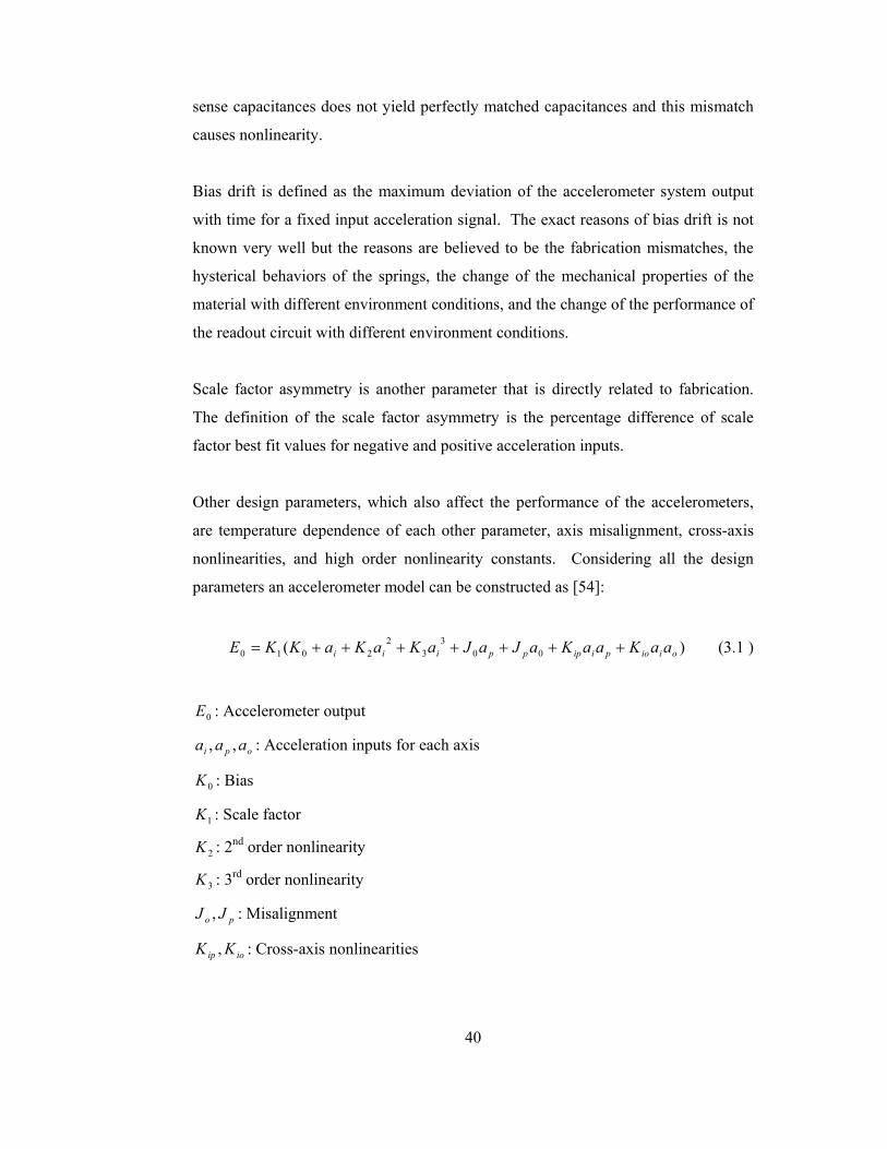
40
sense capacitances does not yield perfectly matched capacitances and this mismatch
causes nonlinearity.
Bias drift is defined as the maximum deviation of the accelerometer system output
with time for a fixed input acceleration signal. The exact reasons of bias drift is not
known very well but the reasons are believed to be the fabrication mismatches, the
hysterical behaviors of the springs, the change of the mechanical properties of the
material with different environment conditions, and the change of the performance of
the readout circuit with different environment conditions.
Scale factor asymmetry is another parameter that is directly related to fabrication.
The definition of the scale factor asymmetry is the percentage difference of scale
factor best fit values for negative and positive acceleration inputs.
Other design parameters, which also affect the performance of the accelerometers,
are temperature dependence of each other parameter, axis misalignment, cross-axis
nonlinearities, and high order nonlinearity constants. Considering all the design
parameters an accelerometer model can be constructed as [54]:
)( 003
32
2010 oiiopiipppiii aaKaaKaJaJaKaKaKKE +++++++= (3.1 )
0E : Accelerometer output
opi aaa ,, : Acceleration inputs for each axis
0K : Bias
1K : Scale factor
2K : 2nd order nonlinearity
3K : 3rd order nonlinearity
po JJ , : Misalignment
ioip KK , : Cross-axis nonlinearities
41
In this study scale factor, bias, total nonlinearity, and resolution are considered as
design parameters. The misalignment in the axis is packaging related problem and is
not considered as a design parameter in this study.
Considering these design parameters, it can be concluded that a proper fabrication is
one of the main issues for high performance accelerometers. A proper fabrication
will significantly reduce undesired nonlinearities. Next important issue is the
readout circuitry because readout circuit plays an important role in the resolution of
the accelerometer. After choosing the process and the readout circuitry, the
mechanical designs can be realized.
3.2 Design Parameters and Challenges for MEMS Gyroscopes
The most common MEMS gyroscope design parameters are resolution, sensitivity
(scale factor), bandwidth, nonlinearity, and bias drift. The definitions of these
parameters are similar to accelerometer parameters with some minor distinctions.
The gyroscope design requires a good topology selection, a well arranged drive and
sense mode resonance frequencies, and a low noise readout circuitry. Due to the fact
that gyroscope topology requires the design of two different resonance modes, the
topology is more complex than the accelerometer topology. The complex topology
also introduces some unwanted resonance modes that causes cross axis sensitivity.
Hence the topology should be carefully designed and should be verified with FEM
simulators. Selecting the topology is also correlated to selecting the resonance
frequencies of drive and sense modes. From the bandwidth-sensitivity trade-off,
either the frequencies should be matched to achieve large sensitivity, or the
frequencies should be slightly mismatched to achieve a wider 3dB bandwidth. To
have matched resonance frequencies, the best solution is to have identical spring
structures and equal masses for these modes, to minimize fabrication errors and
frequency shift due to environmental condition changes. Hence in matched
resonance frequency gyroscope design, the topology should allow to have identical
42
spring structures and identical masses for drive and sense modes. The choice of the
resonance frequencies for these modes is also another design issue. Selecting a low
resonance frequency increases the sensitivity but also increases the effects of
unwanted environment accelerations. To sum up, designing the topology of the
gyroscope is one of the main design challenges that must be carefully handled.
The packaging issue is another design challenge for gyroscopes. In the matched
frequency case, the quality factor of the gyroscope directly includes in the sensitivity
expression. Hence, to achieve high sensitive gyroscopes the design should have a
high quality factor value. The most effective solution to achieve high quality factor
values is to have the sensor vacuum packaged.
The readout part is also very important to have a high performance gyroscope. The
front-end circuit element for the gyroscopes is generally unity gain buffers with low
input capacitances [55]. This buffer should be also very low noise to sense very
small output voltages. The second challenge in the gyroscope readout is the control
loops. These loops start up the drive mode, fix the drive voltage frequency to
resonance frequency of the drive mode, fix the drive mode vibration magnitude, and
cancel out the quadrature error [39].
3.3 Accelerometers and Gyroscopes Designed In This Study
This section explains the accelerometers and gyroscopes designed in this study.
Section 3.3.1 explains the accelerometer topology and gives the FEM simulations for
this topology. Section 3.3.2 explains the gyroscope topology and gives FEM
simulations for this topology. Section 3.3.3 gives the design considerations for three
different processes that are used in this study. Section 3.3.4 gives the performance
estimations for the designed accelerometers and gyroscopes.
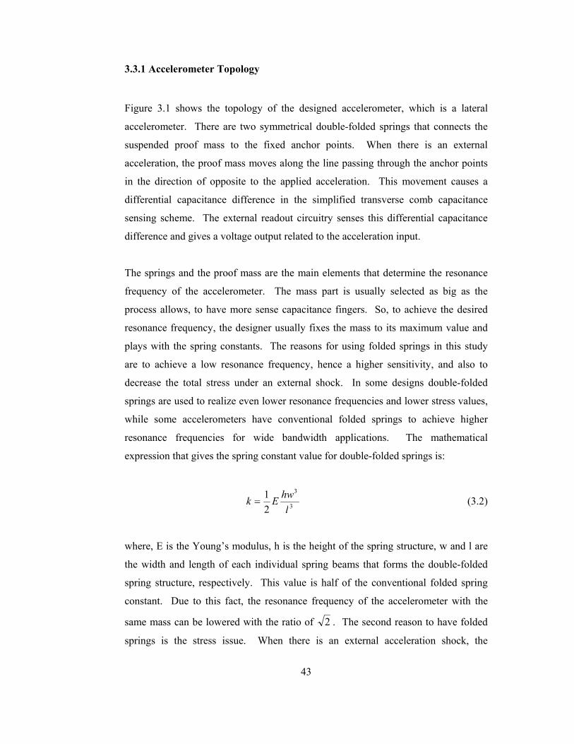
43
3.3.1 Accelerometer Topology
Figure 3.1 shows the topology of the designed accelerometer, which is a lateral
accelerometer. There are two symmetrical double-folded springs that connects the
suspended proof mass to the fixed anchor points. When there is an external
acceleration, the proof mass moves along the line passing through the anchor points
in the direction of opposite to the applied acceleration. This movement causes a
differential capacitance difference in the simplified transverse comb capacitance
sensing scheme. The external readout circuitry senses this differential capacitance
difference and gives a voltage output related to the acceleration input.
The springs and the proof mass are the main elements that determine the resonance
frequency of the accelerometer. The mass part is usually selected as big as the
process allows, to have more sense capacitance fingers. So, to achieve the desired
resonance frequency, the designer usually fixes the mass to its maximum value and
plays with the spring constants. The reasons for using folded springs in this study
are to achieve a low resonance frequency, hence a higher sensitivity, and also to
decrease the total stress under an external shock. In some designs double-folded
springs are used to realize even lower resonance frequencies and lower stress values,
while some accelerometers have conventional folded springs to achieve higher
resonance frequencies for wide bandwidth applications. The mathematical
expression that gives the spring constant value for double-folded springs is:
3
3
21
lhwEk = (3.2)
where, E is the Young’s modulus, h is the height of the spring structure, w and l are
the width and length of each individual spring beams that forms the double-folded
spring structure, respectively. This value is half of the conventional folded spring
constant. Due to this fact, the resonance frequency of the accelerometer with the
same mass can be lowered with the ratio of 2 . The second reason to have folded
springs is the stress issue. When there is an external acceleration shock, the
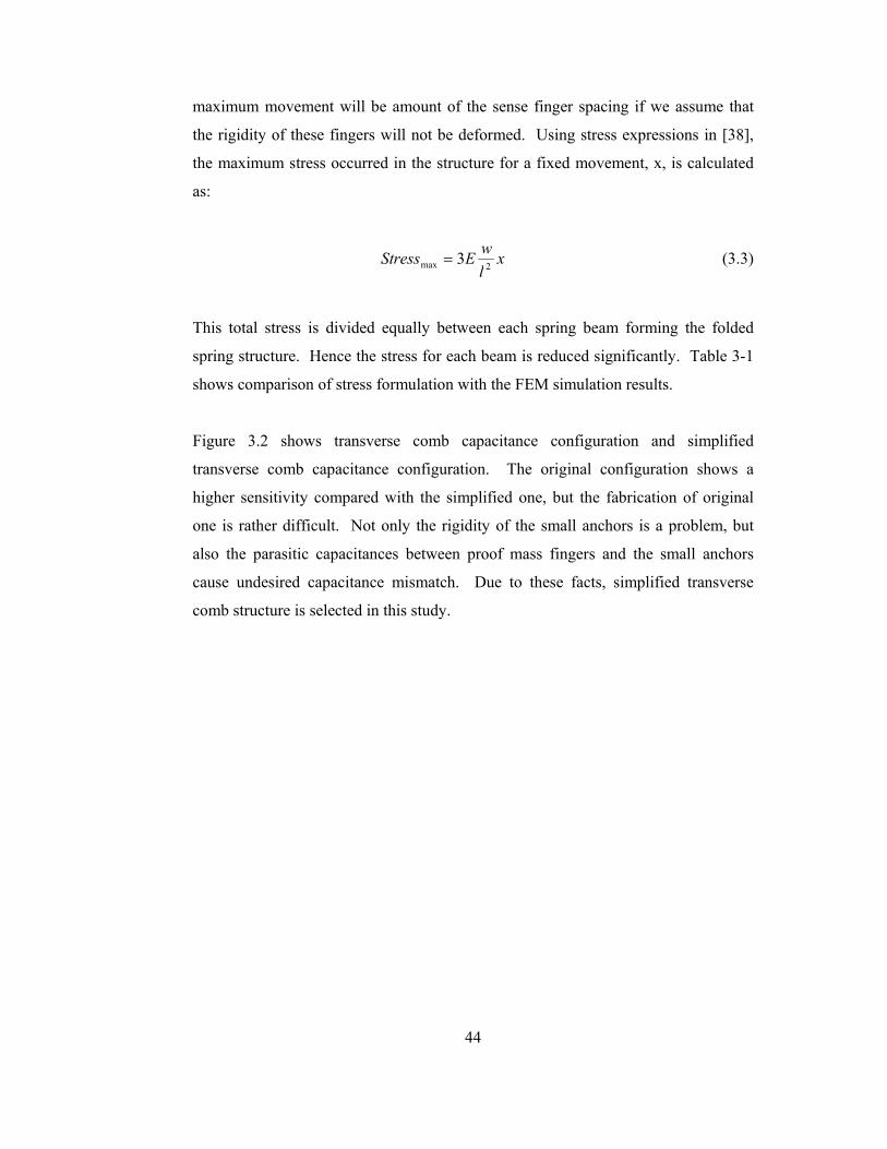
44
maximum movement will be amount of the sense finger spacing if we assume that
the rigidity of these fingers will not be deformed. Using stress expressions in [38],
the maximum stress occurred in the structure for a fixed movement, x, is calculated
as:
xlwEStress 2max 3= (3.3)
This total stress is divided equally between each spring beam forming the folded
spring structure. Hence the stress for each beam is reduced significantly. Table 3-1
shows comparison of stress formulation with the FEM simulation results.
Figure 3.2 shows transverse comb capacitance configuration and simplified
transverse comb capacitance configuration. The original configuration shows a
higher sensitivity compared with the simplified one, but the fabrication of original
one is rather difficult. Not only the rigidity of the small anchors is a problem, but
also the parasitic capacitances between proof mass fingers and the small anchors
cause undesired capacitance mismatch. Due to these facts, simplified transverse
comb structure is selected in this study.
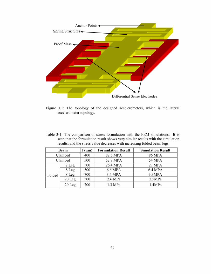
45
Anchor Points Spring Structures
Proof Mass
Differential Sense Electrodes
Figure 3.1: The topology of the designed accelerometers, which is the lateral accelerometer topology.
Table 3-1: The comparison of stress formulation with the FEM simulations. It is seen that the formulation result shows very similar results with the simulation results, and the stress value decreases with increasing folded beam legs.
Beam l (µm) Formulation Result Simulation Result Clamped 400 82.5 MPA 86 MPA Clamped 500 52.8 MPA 54 MPA
2 Leg 500 26.4 MPA 27 MPA 8 Leg 500 6.6 MPA 6.4 MPA 8 Leg 700 3.4 MPA 3.3MPA 20 Leg 500 2.6 MPa 2.5MPa
Folded
20 Leg 700 1.3 MPa 1.4MPa
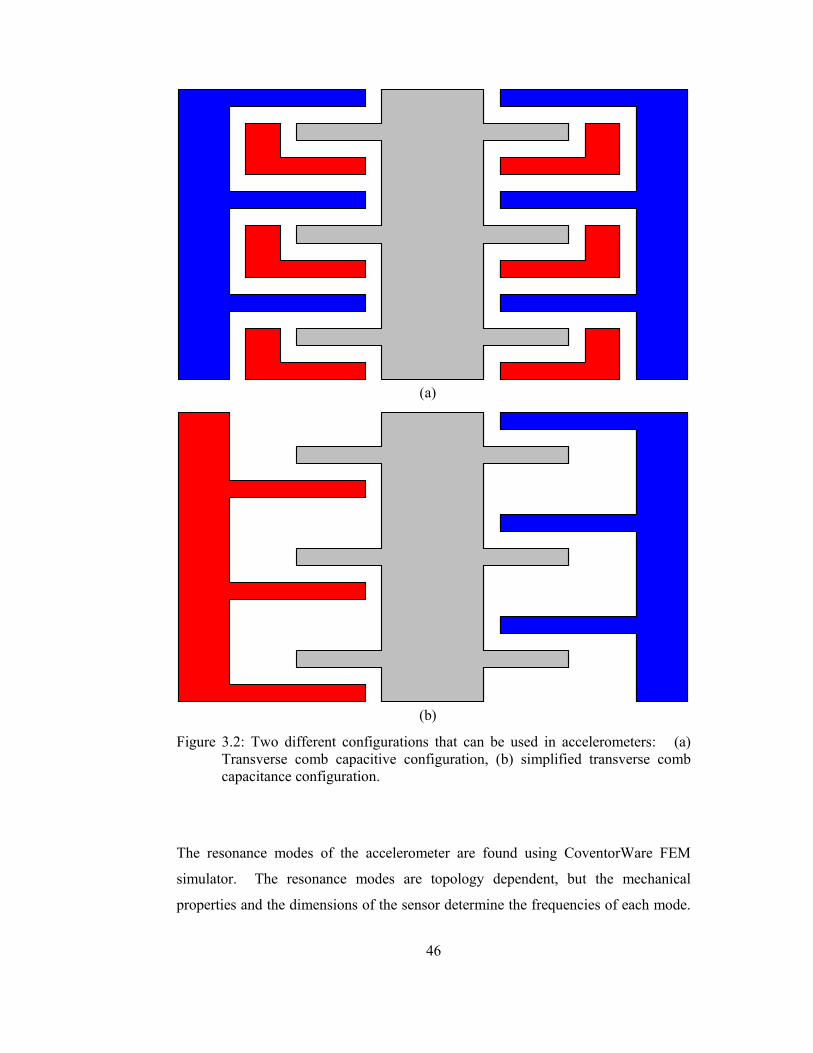
46
(a)
(b) Figure 3.2: Two different configurations that can be used in accelerometers: (a)
Transverse comb capacitive configuration, (b) simplified transverse comb capacitance configuration.
The resonance modes of the accelerometer are found using CoventorWare FEM
simulator. The resonance modes are topology dependent, but the mechanical
properties and the dimensions of the sensor determine the frequencies of each mode.

47
Figure 3.3 shows a FEM simulation result for determining the resonance modes of
the accelerometer topology. This simulation is important to estimate the cross
sensitivity of the accelerometer. The accelerometer should have only one resonance
mode ideally, which is its sensitive mode, but it has also some unwanted resonance
modes. When there is an external acceleration that causes the accelerometer to move
along its unwanted resonance mode, this movement should be as low as possible not
to create cross-axis sensitivity. To achieve that, the difference between resonance
frequencies of sensitive mode and the cross mode should be as high as possible.
(a)
(b) Figure 3.3: FEM simulation results for determining the resonance modes of the
accelerometer topology: (a) the desired sensitivity mode, (b) the unwanted cross mode.
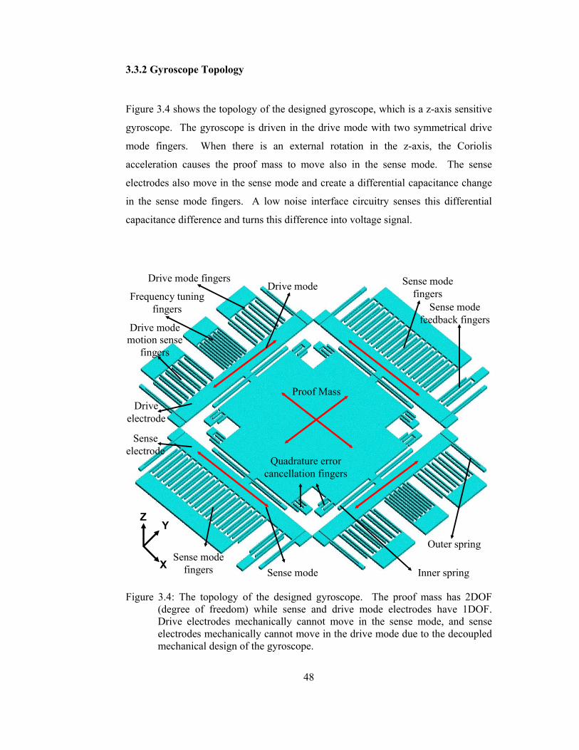
48
3.3.2 Gyroscope Topology
Figure 3.4 shows the topology of the designed gyroscope, which is a z-axis sensitive
gyroscope. The gyroscope is driven in the drive mode with two symmetrical drive
mode fingers. When there is an external rotation in the z-axis, the Coriolis
acceleration causes the proof mass to move also in the sense mode. The sense
electrodes also move in the sense mode and create a differential capacitance change
in the sense mode fingers. A low noise interface circuitry senses this differential
capacitance difference and turns this difference into voltage signal.
Drive mode fingers
Frequency tuning fingers
Drive mode motion sense
fingers
Drive mode Sense mode fingers
Sense mode fingers
Sense mode feedback fingers
Sense mode
Proof Mass
Quadrature error cancellation fingers
Inner spring
Outer spring
Drive electrode
Sense electrode
X
Y Z
Figure 3.4: The topology of the designed gyroscope. The proof mass has 2DOF (degree of freedom) while sense and drive mode electrodes have 1DOF. Drive electrodes mechanically cannot move in the sense mode, and sense electrodes mechanically cannot move in the drive mode due to the decoupled mechanical design of the gyroscope.
49
The gyroscope is a symmetrical and decoupled gyroscope to achieve a high
sensitivity [3]. Springs are all identical in shape in two modes and the drive mode
and the sense mode has the same mass values. This provides a symmetrical
operation. However, due to electrical spring constant difference in sense and drive
mode, and to cancel fabrication errors in resonance frequencies, drive mode has
some frequency tuning fingers. These fingers create an electrical spring constant in
the drive mode and may decrease the drive mode frequency in some range relative to
the applied DC voltage on them [56]. Hence, the drive mode resonance frequency is
designed to be a little more than the sense mode resonance frequency. The
decoupled operation of the gyroscope is provided by the inner and outer springs. The
outer springs connect the electrodes to the anchor points and the inner springs
connect the proof mass to the electrodes. Moreover, the springs are designed so that
the outer springs do not allow the sense electrode to move in the drive mode, and the
drive electrode to move in the sense mode. And the inner springs provides the proof
mass to have 2 degree of freedom. This provides the decoupled operation.
The quadrature error cancellation electrodes are to cancel the misaligned movement
of the proof mass. When the proof mass vibrates in the drive mode, it may have a
motion component in the sense mode due to fabrication errors. This motion
component of the proof mass causes sense mode electrodes to move. Hence, it
causes a differential capacitance difference in the sense mode electrodes and affects
the output. To cancel out this unwanted component, the quadrature error
cancellation electrodes apply proper electrostatic force to the proof mass [51].
The gyroscope has also sense mode feedback fingers. These fingers are designed to
create an analog feedback force to cancel out the sense mode motion [57]. Hence,
when there is an external rotation signal, the Coriolis acceleration forces the proof
mass to move in the sense mode. The inner springs force the sense electrode to
follow the motion of the proof mass in the sense axis. Then, the feedback fingers in
the sense mode give a proper electrostatic force to the sense electrode to cancel this
motion. Hence, the magnitude of the rotation signal is proportional to the magnitude
of the voltage signal applied to the feedback fingers.
50
The resonance modes of the gyroscope topology are found using CoventorWare
FEM simulator. Figure 3.5-7 show the resonance modes of the gyroscope topology.
There are two designed modes which are drive mode and the sense mode. The
resonance frequencies of these modes should be very similar to each other with drive
mode resonance frequency being slightly larger. It can be seen that when the
gyroscope is moving in one mode, the electrode of the other mode does not move.
This is due to decoupled operation. The third mode is the unwanted cross mode.
This mode is a z-axis resonance mode and directly related to the height of the sensor.
Hence, this mode resonance frequency may be larger or lower than the drive and
sense mode resonance frequency due to different processes providing different
sensor heights.
Drive mode fingers have parallel plate capacitance topology. When this topology is
used in the actuators, nonlinear force-displacement characteristics occur. However
this nonlinearity can be negligible if the maximum drive mode displacement is very
small compared to drive mode finger spacing. Due to this fact, drive mode finger
spacing is the biggest spacing in the topology. The frequency tuning fingers are
designed as transverse comb capacitance configuration with both stationary fingers
being applied to same voltage potential. This topology is achieved with connecting
all the stationary fingers to the same anchor.

51
Figure 3.5: Simulation result of sense mode of the gyroscope using CoventorWare FEM simulator. Drive mode electrodes do not move in the sense mode verifying the decoupled operation.
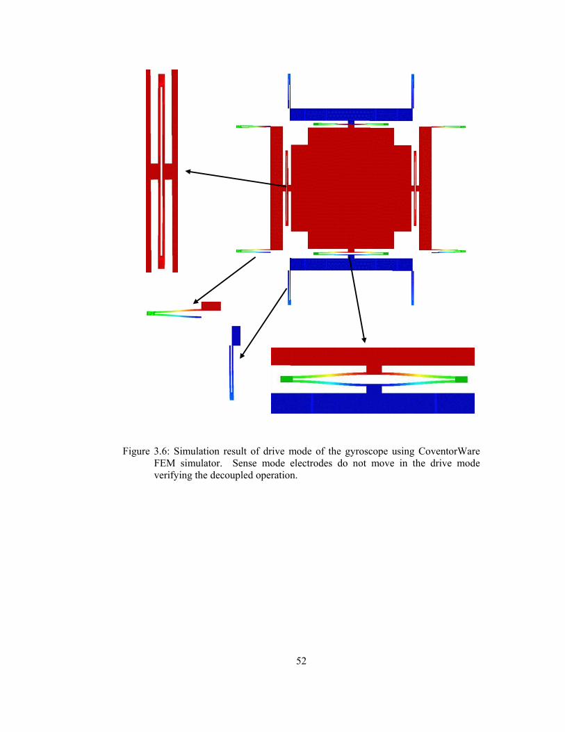
52
Figure 3.6: Simulation result of drive mode of the gyroscope using CoventorWare FEM simulator. Sense mode electrodes do not move in the drive mode verifying the decoupled operation.
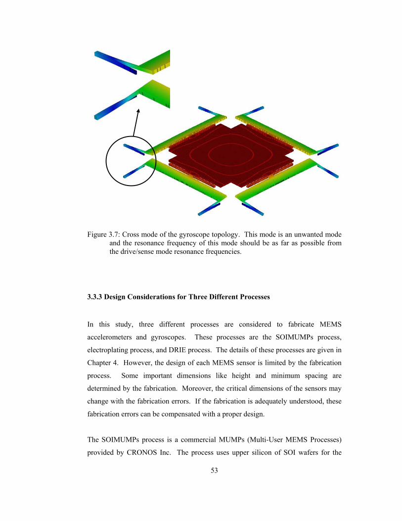
53
Figure 3.7: Cross mode of the gyroscope topology. This mode is an unwanted mode
and the resonance frequency of this mode should be as far as possible from the drive/sense mode resonance frequencies.
3.3.3 Design Considerations for Three Different Processes
In this study, three different processes are considered to fabricate MEMS
accelerometers and gyroscopes. These processes are the SOIMUMPs process,
electroplating process, and DRIE process. The details of these processes are given in
Chapter 4. However, the design of each MEMS sensor is limited by the fabrication
process. Some important dimensions like height and minimum spacing are
determined by the fabrication. Moreover, the critical dimensions of the sensors may
change with the fabrication errors. If the fabrication is adequately understood, these
fabrication errors can be compensated with a proper design.
The SOIMUMPs process is a commercial MUMPs (Multi-User MEMS Processes)
provided by CRONOS Inc. The process uses upper silicon of SOI wafers for the
54
structural material and patterns this layer with DRIE providing 10 µm silicon
structural layer with a 2 µm minimum line and gap spacing [58]. The most important
design considerations are the minimum line and gap spacing, maximum comb finger
length, and die length.
The nickel electroplating process is realized with the facilities in METU-MET. The
process starts with glass wafers and creates patterned nickel structures with
electroplating using a thick photoresist mold. The main design consideration in this
process is the change in the critical dimensions due to the change in the dimensions
of the photoresist mold. During the exposure of the photoresist, the photoresist mold
tries to increase the dimensions of the structural parts and so decrease the dimensions
of the spacing parts. This change in the dimensions is most critical in finger regions
and in spring regions. Without considering this change, the small finger spacing may
vanish due to shrinking, and the resonance frequency of the sensor may come up to
be larger then expected due to the increase of the widths of the springs. With our
previous studies [11], the magnitude of this dimension change is estimated.
Considering a typical mold of thickness more then 15 µm, we can say that the
structural regions try to increase by 1 µm in each direction, hence the spacing parts
try to decrease by 1 µm in each direction. In this study, all the Ni electroplating
designs, calculations, and FEM simulations are done considering this dimension
change.
The DRIE process is also developed to be done at the facilities in METU-MET. The
process starts with a glass wafer. The structural layer is silicon, and it is anodic
bonded to the glass wafer. The DRIE machine patterns the structural layer. The
main design consideration in DRIE process is the silicon etching step. In this step,
the dimensions of the etched parts, which are the spacing parts, tend to increase [18,
59]. This change is the opposite of Ni electroplating process. The magnitude of the
dimension change changes with conditions, and the conditions is not optimized yet
but we consider a change of 1-2 µm [18, 59]. Hence in this study the critical
structural dimensions in DRIE process are designed to be more than desired value
and the critical spacing parts are designed to be smaller than the desired value.
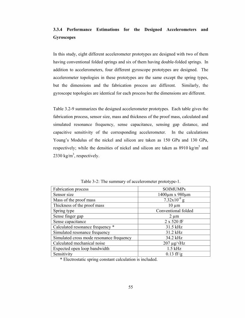
55
3.3.4 Performance Estimations for the Designed Accelerometers and
Gyroscopes
In this study, eight different accelerometer prototypes are designed with two of them
having conventional folded springs and six of them having double-folded springs. In
addition to accelerometers, four different gyroscope prototypes are designed. The
accelerometer topologies in these prototypes are the same except the spring types,
but the dimensions and the fabrication process are different. Similarly, the
gyroscope topologies are identical for each process but the dimensions are different.
Table 3.2-9 summarizes the designed accelerometer prototypes. Each table gives the
fabrication process, sensor size, mass and thickness of the proof mass, calculated and
simulated resonance frequency, sense capacitance, sensing gap distance, and
capacitive sensitivity of the corresponding accelerometer. In the calculations
Young’s Modulus of the nickel and silicon are taken as 150 GPa and 130 GPa,
respectively; while the densities of nickel and silicon are taken as 8910 kg/m3 and
2330 kg/m3, respectively.
Table 3-2: The summary of accelerometer prototype-1.
Fabrication process SOIMUMPs Sensor size 1400µm x 980µm Mass of the proof mass 7.32x10⁻⁹ g Thickness of the proof mass 10 µm Spring type Conventional folded Sense finger gap 2 µm Sense capacitance 2 x 520 fF Calculated resonance frequency * 31.5 kHz Simulated resonance frequency 31.2 kHz Simulated cross mode resonance frequency 34.2 kHz Calculated mechanical noise 207 µg/√Hz Expected open loop bandwidth 1.5 kHz Sensitivity 0.13 fF/g
* Electrostatic spring constant calculation is included.
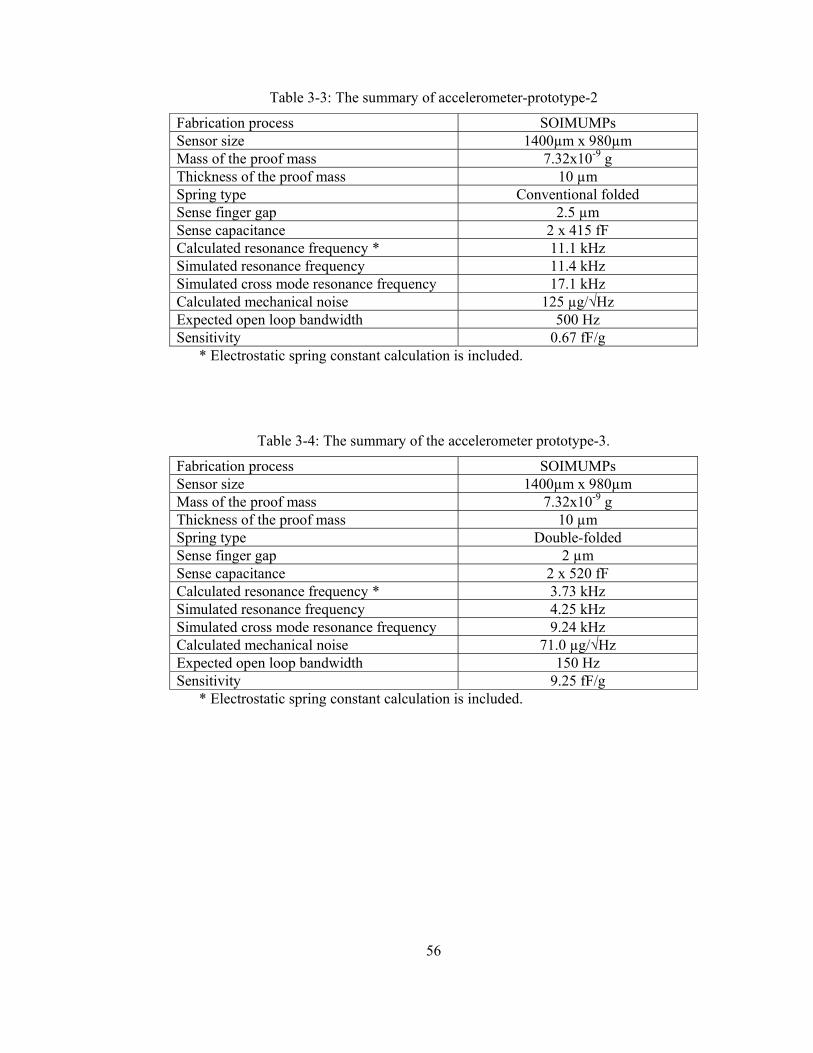
56
Table 3-3: The summary of accelerometer-prototype-2
Fabrication process SOIMUMPs Sensor size 1400µm x 980µm Mass of the proof mass 7.32x10⁻⁹ g Thickness of the proof mass 10 µm Spring type Conventional folded Sense finger gap 2.5 µm Sense capacitance 2 x 415 fF Calculated resonance frequency * 11.1 kHz Simulated resonance frequency 11.4 kHz Simulated cross mode resonance frequency 17.1 kHz Calculated mechanical noise 125 µg/√Hz Expected open loop bandwidth 500 Hz Sensitivity 0.67 fF/g
* Electrostatic spring constant calculation is included.
Table 3-4: The summary of the accelerometer prototype-3.
Fabrication process SOIMUMPs Sensor size 1400µm x 980µm Mass of the proof mass 7.32x10⁻⁹ g Thickness of the proof mass 10 µm Spring type Double-folded Sense finger gap 2 µm Sense capacitance 2 x 520 fF Calculated resonance frequency * 3.73 kHz Simulated resonance frequency 4.25 kHz Simulated cross mode resonance frequency 9.24 kHz Calculated mechanical noise 71.0 µg/√Hz Expected open loop bandwidth 150 Hz Sensitivity 9.25 fF/g
* Electrostatic spring constant calculation is included.
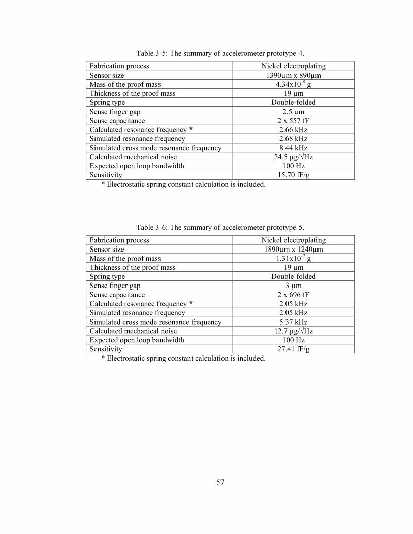
57
Table 3-5: The summary of accelerometer prototype-4.
Fabrication process Nickel electroplating Sensor size 1390µm x 890µm Mass of the proof mass 4.34x10⁻⁸ g Thickness of the proof mass 19 µm Spring type Double-folded Sense finger gap 2.5 µm Sense capacitance 2 x 557 fF Calculated resonance frequency * 2.66 kHz Simulated resonance frequency 2.68 kHz Simulated cross mode resonance frequency 8.44 kHz Calculated mechanical noise 24.5 µg/√Hz Expected open loop bandwidth 100 Hz Sensitivity 15.70 fF/g
* Electrostatic spring constant calculation is included.
Table 3-6: The summary of accelerometer prototype-5.
Fabrication process Nickel electroplating Sensor size 1890µm x 1240µm Mass of the proof mass 1.31x10⁻⁷ g Thickness of the proof mass 19 µm Spring type Double-folded Sense finger gap 3 µm Sense capacitance 2 x 696 fF Calculated resonance frequency * 2.05 kHz Simulated resonance frequency 2.05 kHz Simulated cross mode resonance frequency 5.37 kHz Calculated mechanical noise 12.7 µg/√Hz Expected open loop bandwidth 100 Hz Sensitivity 27.41 fF/g
* Electrostatic spring constant calculation is included.
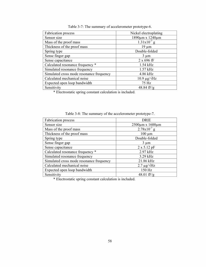
58
Table 3-7: The summary of accelerometer prototype-6.
Fabrication process Nickel electroplating Sensor size 1890µm x 1240µm Mass of the proof mass 1.31x10⁻⁷ g Thickness of the proof mass 19 µm Spring type Double-folded Sense finger gap 3 µm Sense capacitance 2 x 696 fF Calculated resonance frequency * 1.54 kHz Simulated resonance frequency 1.57 kHz Simulated cross mode resonance frequency 4.86 kHz Calculated mechanical noise 10.9 µg/√Hz Expected open loop bandwidth 75 Hz Sensitivity 48.84 fF/g
* Electrostatic spring constant calculation is included.
Table 3-8: The summary of the accelerometer prototype-7.
Fabrication process DRIE Sensor size 2500µm x 1600µm Mass of the proof mass 2.78x10⁻⁷ g Thickness of the proof mass 100 µm Spring type Double-folded Sense finger gap 3 µm Sense capacitance 2 x 5.12 pF Calculated resonance frequency * 2.97 kHz Simulated resonance frequency 3.29 kHz Simulated cross mode resonance frequency 21.86 kHz Calculated mechanical noise 2.7 µg/√Hz Expected open loop bandwidth 150 Hz Sensitivity 48.01 fF/g
* Electrostatic spring constant calculation is included.
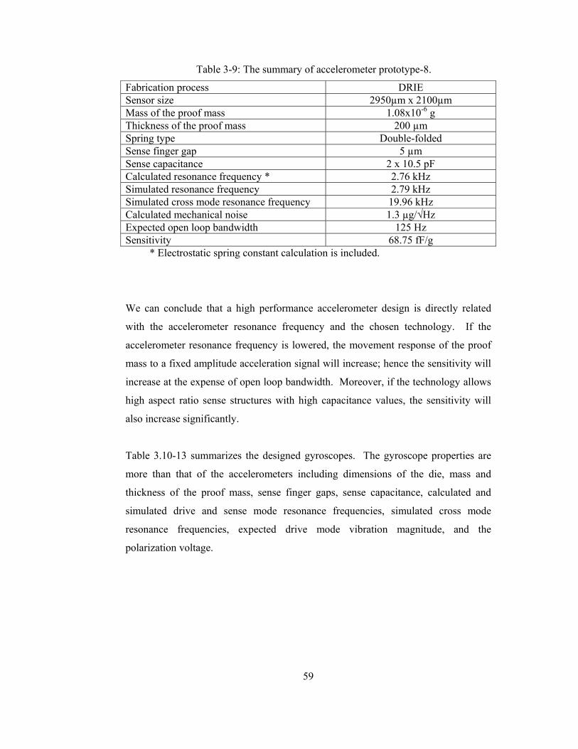
59
Table 3-9: The summary of accelerometer prototype-8.
Fabrication process DRIE Sensor size 2950µm x 2100µm Mass of the proof mass 1.08x10⁻⁶ g Thickness of the proof mass 200 µm Spring type Double-folded Sense finger gap 5 µm Sense capacitance 2 x 10.5 pF Calculated resonance frequency * 2.76 kHz Simulated resonance frequency 2.79 kHz Simulated cross mode resonance frequency 19.96 kHz Calculated mechanical noise 1.3 µg/√Hz Expected open loop bandwidth 125 Hz Sensitivity 68.75 fF/g
* Electrostatic spring constant calculation is included.
We can conclude that a high performance accelerometer design is directly related
with the accelerometer resonance frequency and the chosen technology. If the
accelerometer resonance frequency is lowered, the movement response of the proof
mass to a fixed amplitude acceleration signal will increase; hence the sensitivity will
increase at the expense of open loop bandwidth. Moreover, if the technology allows
high aspect ratio sense structures with high capacitance values, the sensitivity will
also increase significantly.
Table 3.10-13 summarizes the designed gyroscopes. The gyroscope properties are
more than that of the accelerometers including dimensions of the die, mass and
thickness of the proof mass, sense finger gaps, sense capacitance, calculated and
simulated drive and sense mode resonance frequencies, simulated cross mode
resonance frequencies, expected drive mode vibration magnitude, and the
polarization voltage.
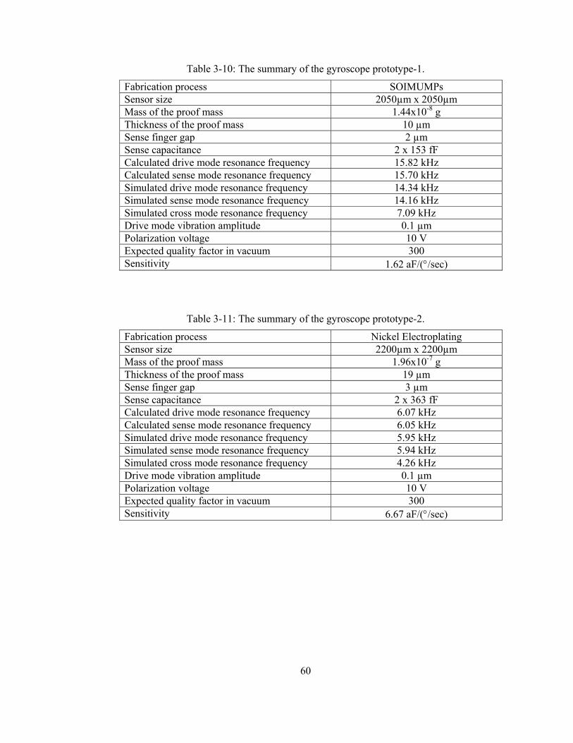
60
Table 3-10: The summary of the gyroscope prototype-1.
Fabrication process SOIMUMPs Sensor size 2050µm x 2050µm Mass of the proof mass 1.44x10⁻⁸ g Thickness of the proof mass 10 µm Sense finger gap 2 µm Sense capacitance 2 x 153 fF Calculated drive mode resonance frequency 15.82 kHz Calculated sense mode resonance frequency 15.70 kHz Simulated drive mode resonance frequency 14.34 kHz Simulated sense mode resonance frequency 14.16 kHz Simulated cross mode resonance frequency 7.09 kHz Drive mode vibration amplitude 0.1 µm Polarization voltage 10 V Expected quality factor in vacuum 300 Sensitivity 1.62 aF/(°/sec)
Table 3-11: The summary of the gyroscope prototype-2.
Fabrication process Nickel Electroplating Sensor size 2200µm x 2200µm Mass of the proof mass 1.96x10⁻⁷ g Thickness of the proof mass 19 µm Sense finger gap 3 µm Sense capacitance 2 x 363 fF Calculated drive mode resonance frequency 6.07 kHz Calculated sense mode resonance frequency 6.05 kHz Simulated drive mode resonance frequency 5.95 kHz Simulated sense mode resonance frequency 5.94 kHz Simulated cross mode resonance frequency 4.26 kHz Drive mode vibration amplitude 0.1 µm Polarization voltage 10 V Expected quality factor in vacuum 300 Sensitivity 6.67 aF/(°/sec)
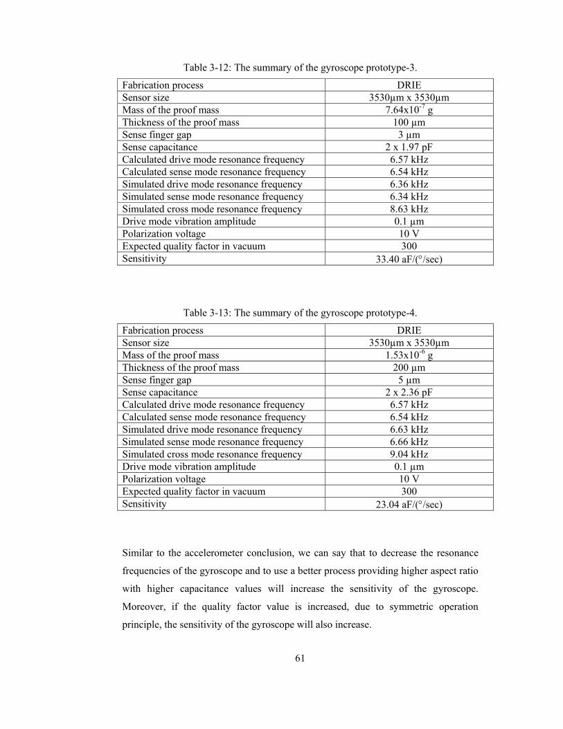
61
Table 3-12: The summary of the gyroscope prototype-3.
Fabrication process DRIE Sensor size 3530µm x 3530µm Mass of the proof mass 7.64x10⁻⁷ g Thickness of the proof mass 100 µm Sense finger gap 3 µm Sense capacitance 2 x 1.97 pF Calculated drive mode resonance frequency 6.57 kHz Calculated sense mode resonance frequency 6.54 kHz Simulated drive mode resonance frequency 6.36 kHz Simulated sense mode resonance frequency 6.34 kHz Simulated cross mode resonance frequency 8.63 kHz Drive mode vibration amplitude 0.1 µm Polarization voltage 10 V Expected quality factor in vacuum 300 Sensitivity 33.40 aF/(°/sec)
Table 3-13: The summary of the gyroscope prototype-4.
Fabrication process DRIE Sensor size 3530µm x 3530µm Mass of the proof mass 1.53x10⁻⁶ g Thickness of the proof mass 200 µm Sense finger gap 5 µm Sense capacitance 2 x 2.36 pF Calculated drive mode resonance frequency 6.57 kHz Calculated sense mode resonance frequency 6.54 kHz Simulated drive mode resonance frequency 6.63 kHz Simulated sense mode resonance frequency 6.66 kHz Simulated cross mode resonance frequency 9.04 kHz Drive mode vibration amplitude 0.1 µm Polarization voltage 10 V Expected quality factor in vacuum 300 Sensitivity 23.04 aF/(°/sec)
Similar to the accelerometer conclusion, we can say that to decrease the resonance
frequencies of the gyroscope and to use a better process providing higher aspect ratio
with higher capacitance values will increase the sensitivity of the gyroscope.
Moreover, if the quality factor value is increased, due to symmetric operation
principle, the sensitivity of the gyroscope will also increase.
62
3.4 Summary
This chapter presents the design considerations of MEMS accelerometers and
gyroscopes and explains the designed sensors. In MEMS accelerometers and
gyroscopes, the main considerations for the evaluation of the sensor are the
resolution, scale factor, bias drift, and bandwidth. To realize a high performance
sensor, each design consideration must be handled carefully.
In this study, we have designed 8 accelerometer prototypes, and 4 gyroscope
prototypes. For the realization of these prototypes, we have used three different
fabrication processes. The fabrication errors from these processes are also
considered in each design. The next chapter explains the details of the fabrication
processes used in this study.

63
CHAPTER 4
MEMS ACCELEROMETERS AND GYROSCOPES
FABRICATION
This chapter gives the details of fabrication steps of the processes used in this study.
Section 4.1 gives an introduction to the MEMS fabrication techniques. Section 4.2
explains the SOIMUMPs process in detail, and gives the structural dimensions.
Section 4.3 gives the details of nickel electroplating process, and explains the
material layers that we use in this process. Section 4.4 explains the DRIE process.
Finally, Section 4.5 gives a summary of this chapter.
4.1 Introduction to MEMS Fabrication Techniques
MEMS fabrication or micromachining refers to fabrication of devices with at least
one of their dimensions in micrometer range with the help of etching techniques to
remove part of the substrate or deposit thin film [60-61]. There are basically two
micromachining techniques: bulk and surface micromachining.
In bulk micromachining, the wafer is etched deeply from either front or back side.
However, the surface micromachining tries to build up structures onto the wafer with
depositing techniques. Although the definitions of these micromachining techniques
seem to be clear, it is not easy to say whether a process is surface or bulk
64
micromachining due to the fact that the process can use proper steps from both
surface and bulk micromachining.
The bulk micromachining is usually realized using silicon substrate. There are
various methods to etch silicon using wet or dry silicon etching techniques [62]. In
the early times when the researchers used bulk micromachining to form MEMS
sensors, they used wet etchants to etch silicon. The etchants may realize an isotropic
etching where the silicon is etched with the same etch rate in each directions, or
anisotropic etch, where the etch rates in different crystalline planes of silicon is
significantly different. But, with wet etching, vertical comb fingers with high aspect
ratio capacitances cannot be obtained. Moreover, wet etching, especially isotropic
wet etching is not very controllable. In addition, the etchants may be dangerous for
human health (EDP), or be problematic for the CMOS circuitry (KOH). However,
the main advantageous of wet etching is to realize very thick proof mass structures
easily. After the realization of the RIE machine (Reactive Ion Etching), the
possibility of forming vertical comb structures is born, but the RIE machine could
not handle high thicknesses. Finally, DRIE machine solved this problem creating
very high trenches with high aspect ratio capacitances [63].
The surface micromachining uses thin film deposition techniques and then etches
sacrificial layers to create suspended mechanical structures [26]. The process steps
of surface micromachining are similar to CMOS circuitry fabrication, and hence the
main advantage of surface micromachining is its compatibility with the standard IC
process. In addition to this, the vertical comb fingers can be easily realized with this
technique. However, the main disadvantage of the surface micromachining is the
thin structural layer thicknesses and stress issues due to these thin films. But, with
the advanced machines like DRIE, or using high aspect ratio high thickness
photoresist for structural layer mold in electroplating process started to remove this
disadvantage of the surface micromachining with providing high thickness proof
masses [64].
65
There are various accelerometers and gyroscopes fabricated with bulk [65-68] or
surface micromachining [69-73]. Moreover, some sophisticated processes are
developed using both surface and bulk micromachining for realization of MEMS
sensors [74-75].
4.2 Details of SOIMUMPs Process
SOIMUMPs process is a commercial MUMPs (Multi-User MEMS Processes)
provided by CRONOS Inc. Figure 4.1 shows the overview of the SOIMUMPs
process. The process uses an SOI (Silicon on Insulator) wafer and patterns the top
silicon layer for the structural layer. The process starts with the phosphorus doping
of top silicon layer. This doping is to arrange the resistivity values of the silicon
layer. After this step, Cr/Au metal layer is patterned. For this layer, first a negative
photoresist is coated, exposed, and developed according to metal mask, and then
Cr/Au is e-beam evaporated. A successful lift-off step patterns the metal layer.
After first metallization, structural layer is patterned. To achieve this, masking
photoresist is coated, exposed and developed according to structural mask. After
lithography, the structural silicon is etched with DRIE up to the oxide layer. After
this point, the front part of the wafer is coated with a protective layer and a masking
photoresist layer is patterned on to the backside of the layer. The bulk silicon part of
the wafer is etched all the way with DRIE up to the oxide layer. This etching defines
the suspended regions of the sensors. After this step the oxide layer and the
protective layer is etched. From this point on, the substrate connection can be
achieved and the structures are suspended. A shadow mask technique is used to
pattern second metallization which provides substrate connection. The process ends
after the shadow mask is removed.
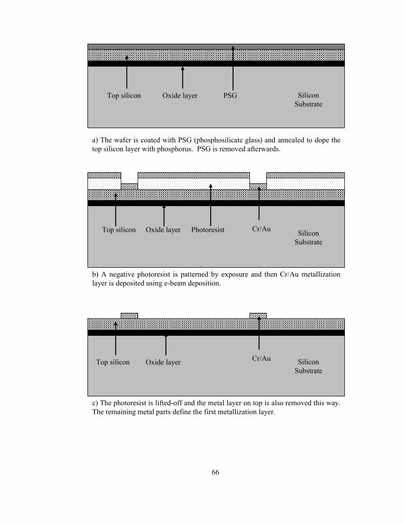
66
a) The wafer is coated with PSG (phosphosilicate glass) and annealed to dope the top silicon layer with phosphorus. PSG is removed afterwards.
b) A negative photoresist is patterned by exposure and then Cr/Au metallization layer is deposited using e-beam deposition.
c) The photoresist is lifted-off and the metal layer on top is also removed this way. The remaining metal parts define the first metallization layer.
Top silicon Oxide layer PSG Silicon Substrate
Top silicon Oxide layer Silicon Substrate
Photoresist
Top silicon Oxide layer Silicon Substrate
Cr/Au
Cr/Au
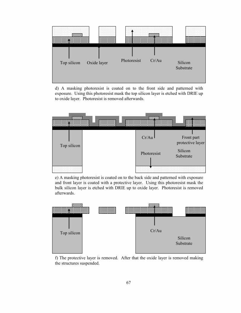
67
d) A masking photoresist is coated on to the front side and patterned with exposure. Using this photoresist mask the top silicon layer is etched with DRIE up to oxide layer. Photoresist is removed afterwards.
e) A masking photoresist is coated on to the back side and patterned with exposure and front layer is coated with a protective layer. Using this photoresist mask the bulk silicon layer is etched with DRIE up to oxide layer. Photoresist is removed afterwards.
f) The protective layer is removed. After that the oxide layer is removed making the structures suspended.
Oxide layer Silicon Substrate
Cr/Au Top silicon Photoresist
Silicon Substrate
Cr/Au
Top silicon
Photoresist
Front part protective layer
Silicon Substrate
Cr/Au Top silicon
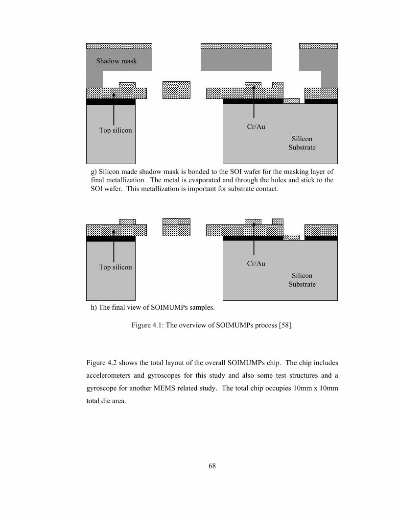
68
g) Silicon made shadow mask is bonded to the SOI wafer for the masking layer of final metallization. The metal is evaporated and through the holes and stick to the SOI wafer. This metallization is important for substrate contact.
h) The final view of SOIMUMPs samples.
Silicon Substrate
Cr/Au Top silicon
Shadow mask
Silicon Substrate
Cr/Au Top silicon
Figure 4.1: The overview of SOIMUMPs process [58].
Figure 4.2 shows the total layout of the overall SOIMUMPs chip. The chip includes
accelerometers and gyroscopes for this study and also some test structures and a
gyroscope for another MEMS related study. The total chip occupies 10mm x 10mm
total die area.

69
Acc
eler
omet
er
Gyr
osco
pe
Figure 4.2: The overall layout of SOIMUMPs chip. The chip includes accelerometers and gyroscopes for this study and also some test structures and a gyroscope for another study. The chip occupies 10mm x 10mm total chip area.
Table 4-1 gives the thicknesses and purposes of material layers in SOIMUMPs
process. The main advantage of this process is using single crystal silicon as its
structural layer. Single crystal silicon shows great mechanical and electrical
properties and is highly preferred is MEMS devices [26]. Moreover, DRIE
patterning on the front size provide 5 aspect ratio capacitive walls for vertical comb
structures. Combining this moderately high aspect ratio with 10 µm structural height,
reasonably high capacitances can be achieved with this process. Due to these
70
advantages, we have chosen SOIMUMPs process as one of the fabrication processes
for realizing our sensors.
Table 4-1: Thicknesses and purposes of material layers in SOIMUMPs process [58].
Material Layer Thickness (µm) Purpose Metal 1 (Cr/Au) 0.52 Provides electrical connections.
Top silicon 10 Structural silicon layer. Oxide 1.0 Substrate isolation.
Silicon substrate 400 Substrate. Metal 2 (Cr/Au) 0.65 Provides substrate connection.
4.3 Details of Nickel Electroplating Process
The nickel electroplating process used in this study is a surface micromachining
process which is developed in the facilities of METU-MET. The fabrication steps of
this process are leaded by Said Emre Alper, and realizing these steps is also a part of
this study. Figure 4.3 shows the overall fabrication details of nickel electroplating
process. The process uses glass as the substrate layer and nickel as the structural
layer. The structural nickel is formed using electroplating with the help of thick
photoresist mold.
Table 4-2 gives the thicknesses and purposes of material layers in nickel
electroplating process. The use of a glass substrate is one of the major advantages of
this process due to the fact that glass being an insulator will not cause parasitic
capacitances in the pad regions and will not cause levitation effect [76]. In addition
to this advantage, the electroplating process provides a high possibility of material
choices due to the fact that photoresist mold provides the possibility of electroplating
various metals for various purposes. In this process, nickel is selected for the
structural material for its attractive material properties such as Young’s modulus and
yield strength [11, 77]. Moreover, gold is suitable for interconnect material due to its
high conductivity and ease of fabrication [78].
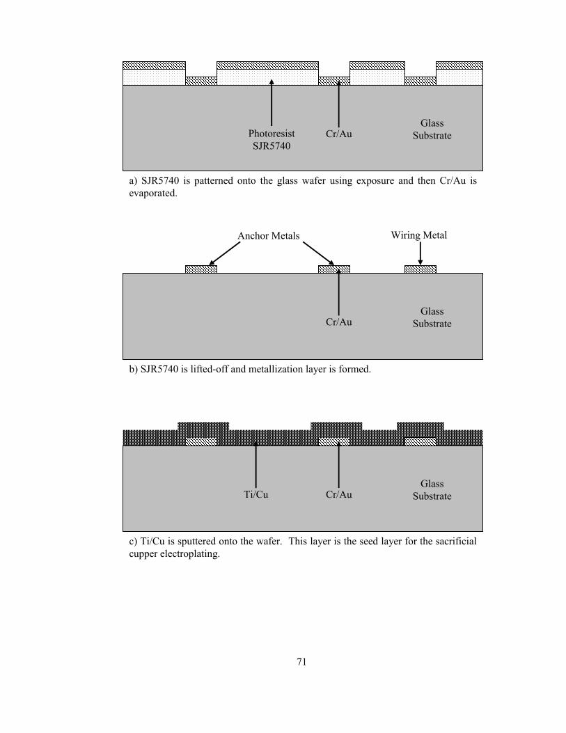
71
a) SJR5740 is patterned onto the glass wafer using exposure and then Cr/Au is evaporated.
b) SJR5740 is lifted-off and metallization layer is formed.
c) Ti/Cu is sputtered onto the wafer. This layer is the seed layer for the sacrificial cupper electroplating.
Glass Substrate Photoresist
SJR5740 Cr/Au
Glass Substrate Cr/Au
Anchor Metals Wiring Metal
Glass Substrate Cr/Au Ti/Cu
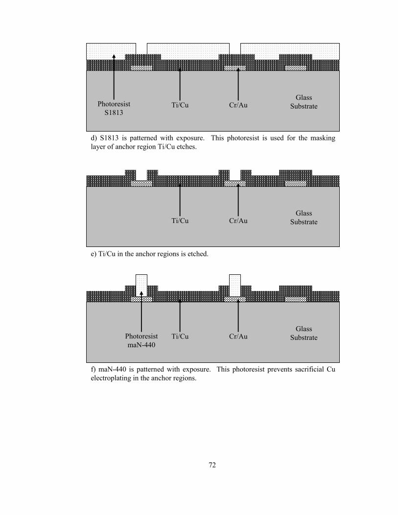
72
d) S1813 is patterned with exposure. This photoresist is used for the masking layer of anchor region Ti/Cu etches.
e) Ti/Cu in the anchor regions is etched.
f) maN-440 is patterned with exposure. This photoresist prevents sacrificial Cu electroplating in the anchor regions.
Glass Substrate Cr/Au Ti/Cu Photoresist
S1813
Glass Substrate Cr/Au Ti/Cu
Glass Substrate Cr/Au Ti/Cu Photoresist
maN-440
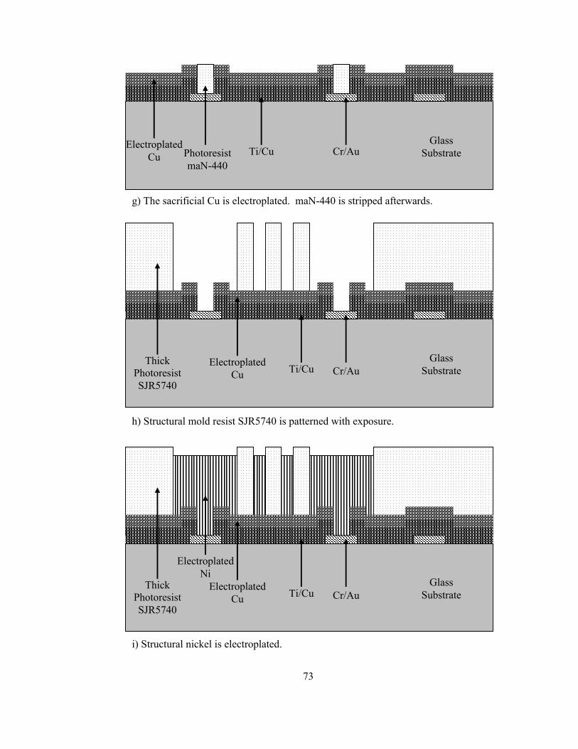
73
g) The sacrificial Cu is electroplated. maN-440 is stripped afterwards.
h) Structural mold resist SJR5740 is patterned with exposure.
i) Structural nickel is electroplated.
Glass Substrate Cr/Au Ti/Cu Photoresist
maN-440
Electroplated Cu
Glass Substrate Ti/Cu Electroplated
Cu Cr/Au Thick
Photoresist SJR5740
Glass Substrate Ti/Cu Electroplated
Cu Cr/Au Thick
Photoresist SJR5740
Electroplated Ni
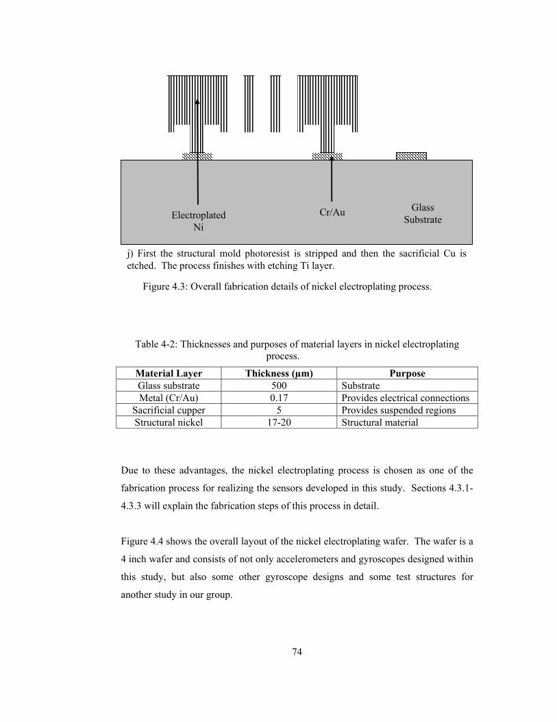
74
j) First the structural mold photoresist is stripped and then the sacrificial Cu is etched. The process finishes with etching Ti layer.
Glass Substrate
Cr/Au Electroplated Ni
Figure 4.3: Overall fabrication details of nickel electroplating process.
Table 4-2: Thicknesses and purposes of material layers in nickel electroplating process.
Material Layer Thickness (µm) Purpose Glass substrate 500 Substrate Metal (Cr/Au) 0.17 Provides electrical connections
Sacrificial cupper 5 Provides suspended regions Structural nickel 17-20 Structural material
Due to these advantages, the nickel electroplating process is chosen as one of the
fabrication process for realizing the sensors developed in this study. Sections 4.3.1-
4.3.3 will explain the fabrication steps of this process in detail.
Figure 4.4 shows the overall layout of the nickel electroplating wafer. The wafer is a
4 inch wafer and consists of not only accelerometers and gyroscopes designed within
this study, but also some other gyroscope designs and some test structures for
another study in our group.
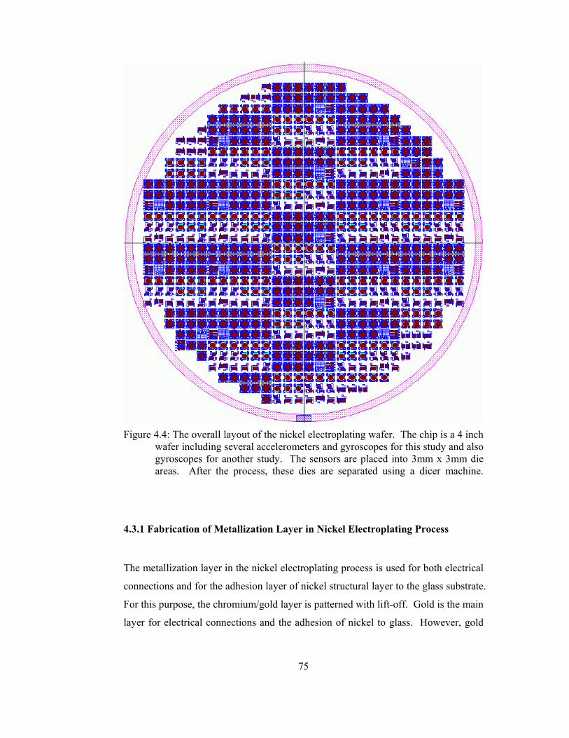
75
Figure 4.4: The overall layout of the nickel electroplating wafer. The chip is a 4 inch
wafer including several accelerometers and gyroscopes for this study and also gyroscopes for another study. The sensors are placed into 3mm x 3mm die areas. After the process, these dies are separated using a dicer machine.
4.3.1 Fabrication of Metallization Layer in Nickel Electroplating Process
The metallization layer in the nickel electroplating process is used for both electrical
connections and for the adhesion layer of nickel structural layer to the glass substrate.
For this purpose, the chromium/gold layer is patterned with lift-off. Gold is the main
layer for electrical connections and the adhesion of nickel to glass. However, gold
76
needs an adhesion layer between itself and glass substrate and hence chromium is
used for this purpose.
The metallization process is the first process step and realized with lift-off. The
process starts with the preparation of the glass wafer. The wafer is first put into
piranha etchant (1:1 H2SO4:H2O2) for 15 min for organic cleaning. After this step,
the wafer is dipped into BHF (Buffered HF, 6:1 NH4:HF) for 30 sec. This step is
important for the adhesion of chromium to the glass substrate. BHF slowly etches
the glass and creates a rough surface. This rough surface increases the adhesion of
chromium to the glass surface.
After the preparation of the glass wafer, the wafer is coated with 7-8 µm SJR5740
photoresist. This photoresist is patterned with exposure. After development, the
anchor regions and the routing metal regions will be developed, while in all the
remaining regions the photoresist will remain. The wafer is then put into evaporation
machine and first chromium (200 Å) then gold (1500 Å) is evaporated (Figure 4.3
(a)).
Evaporation does not have good step coverage; however this property of evaporation
turns out to be advantageous in lift-off process. The wafer is put into a petry dish
full of acetone and with the help of ultrasonic buzzer the photoresist and the metal
layer on top of photoresist is lifted-off (Figure 4.3 (b)). After this step the
metallization layer is formed. This layer provides electrical connections and also is
used as an adhesion layer of nickel to glass substrate.
4.3.2 Fabrication of Sacrificial Layer in Nickel Electroplating Process
The sacrificial layer in the electroplating process provides suspended regions of the
sensor. For selecting the sacrificial layer, a thick sacrificial layer is preferred to
achieve lower air damping. Moreover, a more important issue is the etchant that
etches the sacrificial layer. The etchant should not deform other materials while
77
etching the sacrificial layer. According to these criteria, cupper is selected as the
sacrificial layer.
The sacrificial layer covers the entire wafer except the anchor regions. To achieve
this, the cupper is electroplated while the anchor regions are filled with a proper
photoresist. Hence, the sacrificial formation process starts with the formation of seed
layer for cupper electroplating. The wafer is put into the sputtering machine for
titanium/cupper (300 Å / 3000 Å) seed layer sputtering. The main seed layer is
cupper, but to achieve a good adhesion between glass substrate and cupper, titanium
layer is used. After sputtering (Figure 4.3 (c)), to etch the titanium/cupper in the
anchor regions, S1813 thin photoresist is patterned with exposure (Figure 4.3 (d)).
With S1813 masking layer, the sputtered metal layers in the anchor regions are
removed by first cupper etch (1:1:18 CH3HOOH:H2O2:DI H2O) and then titanium
etch (1:1:600 HF:H2O2:DI H2O) (Figure 4.3 (e)). After these etchings, the masking
photoresist is removed.
After preparation of the seed layer, the wafer is coated with maN-440 negative
photoresist and patterned with exposure. This time the photoresist in the anchor
regions remained in the other regions the photoresist is developed (Figure 4.3 (f)).
This remaining photoresist prevents sacrificial cupper electroplating in the anchor
regions. After the development, 5 µm thick sacrificial cupper of is electroplated
(Figure 4.3 (g)). The fabrication of sacrificial layer finishes with the removing of the
photoresist.
4.3.3 Fabrication of Structural Layer in Nickel Electroplating Process
The fabrication of the structural layer in the electroplating process is achieved by
first patterning the mold photoresist, then electroplating the structural nickel, and
finally stripping the stripping the mold photoresist and the sacrificial layer.
The structural mold formation is one of the most critical steps of the whole process.
This step defines the aspect ratio of the sensor, as it defines the structural part and

78
spacing part in the comb finger regions. To achieve a high aspect ratio, and high
proof mass thicknesses, the photoresist mold should be thick and can be patterned
with high aspect ratio. SJR5740 is a thick photoresist that can realize these
conditions [79]. In the literature, there are some studies that achieved 6.8 aspect ratio
structures [80].
For the formation of the mold, first SJR5740 is coated with a low spin rate. After
this step, the wafer should wait on the chuck of the spinner for a while until the stress
related lines on the photoresist surface vanishes. After this waiting period, the wafer
is softbaked on the hotplate. After softbake, there is relaxation time period for this
photoresist in high humidity levels. To achieve this level, we put few water drops in
a wafer holder, put the wafers in this holder, close the holder, and wait for 2 hours.
After this relaxation time, exposure is done. There is another relaxation period after
the exposure again in the high humidity levels for 2 hours. After this relaxation
period, the development can be done (Figure 4.3 (h)).
After the formation of the mold photoresist, the mold should be hardbaked. This
bake is prevents deformation of the mold photoresist in the nickel electroplating
solution. However, SJR5740 is sensitive to high temperatures and if applied to high
temperatures, it deforms its shape. To avoid any shape change due to hardbake, the
wafer is applied to 80 °C for 16 hours. With this hardbake, the photoresist shape
changes a little in the bulky photoresist regions, but it withstands the electroplating
solution.
The next step is the nickel electroplating step. We have made several electroplating
trials with dummy wafers to achieve the optimum nickel electroplating conditions.
The applied current, the agents in the solution are important effects in the nickel
electroplating process, and playing with these conditions we have achieved very
shiny and low stress nickel structures (Figure 4.3 (i)).
The process finishes with removing all the sacrificial layers. However, due to the
fact that dicing of the wafer may cause damage to the suspended structures, the

79
release operation is done after dicing. However, we have observed that, the cupper
sacrificial layer is deformed in the dicing operation, and deformed cupper also
deforms the metal pads underneath. To avoid this problem, before the dicing
operation, the cupper in the pad regions should be etched away, but the samples
should not be totally released not to cause any damage in the dicing operation.
Hence, first mold photoresist is stripped, and then sacrificial cupper is etched half
way. Due to the fact that the cupper in the open regions are gone first, with a proper
timing, we have achieved to remove the cupper in the pad regions while keep the
cupper under the devices. After the half cupper etch, the wafer is coated with a
protective photoresist and then diced. After dicing, the release operation is done
sample by sample. First, the protective photoresist is removed, then the remaining
cupper is etched away, then the titanium layer under the cupper layer is etched. After
titanium etch, the samples are totally released. Not to cause any stiction problem, the
last step is to dip the samples into IPA, and evaporate the IPA on the hot plate.
Figure 4.3 (i) shows the final view of the electroplated samples.
4.4 Details of DRIE Process
The DRIE process is an advanced process that uses bulk micromachining. The DRIE
process is currently being developed in the facilities of METU-MET. The
fabrication steps of this process are leaded by Said Emre Alper, and realizing these
steps is also a part of this study. Figure 4.5 shows the overall fabrication details of
the DRIE process. This process uses glass substrate similar to nickel electroplating
process. The silicon wafer that will be used as the structural layer is bonded onto the
glass wafer with anodic bonding and then silicon is etched from the top with DRIE
machine. Most of the process steps in the DRIE process have been completed. The
DRIE tool that is necessary for the deep trench etching in silicon is also purchased,
and the installation of it is still continuing.
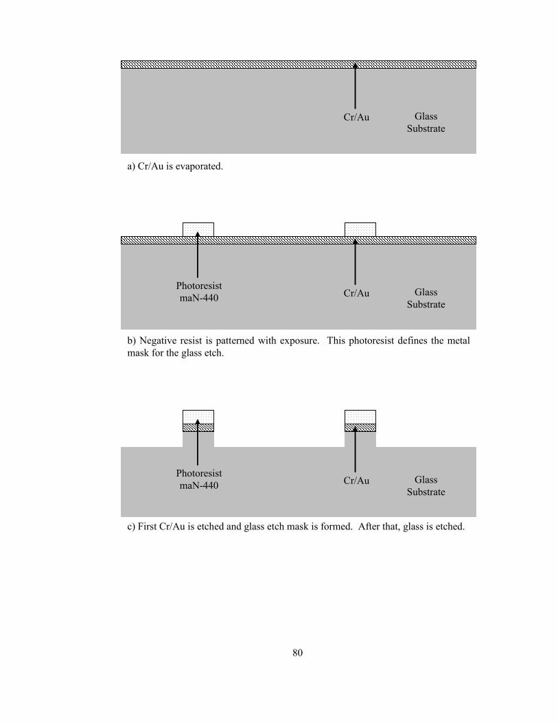
80
a) Cr/Au is evaporated.
b) Negative resist is patterned with exposure. This photoresist defines the metal mask for the glass etch.
c) First Cr/Au is etched and glass etch mask is formed. After that, glass is etched.
Glass Substrate
Cr/Au
Glass Substrate
Cr/Au Photoresist maN-440
Glass Substrate
Cr/Au Photoresist maN-440
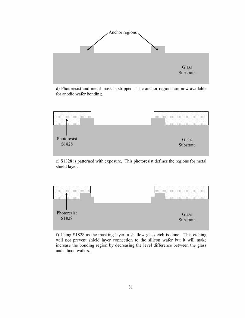
81
d) Photoresist and metal mask is stripped. The anchor regions are now available for anodic wafer bonding.
e) S1828 is patterned with exposure. This photoresist defines the regions for metal shield layer.
f) Using S1828 as the masking layer, a shallow glass etch is done. This etching will not prevent shield layer connection to the silicon wafer but it will make increase the bonding region by decreasing the level difference between the glass and silicon wafers.
Glass Substrate
Anchor regions
Glass Substrate
Photoresist S1828
Photoresist S1828
Glass Substrate
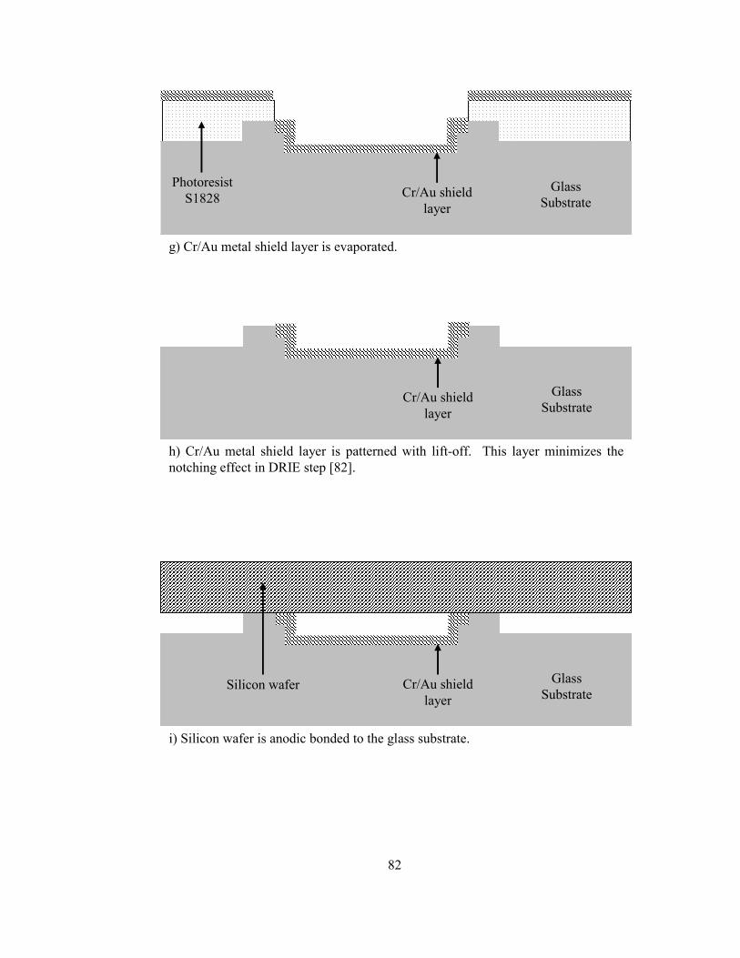
82
g) Cr/Au metal shield layer is evaporated.
h) Cr/Au metal shield layer is patterned with lift-off. This layer minimizes the notching effect in DRIE step [82].
i) Silicon wafer is anodic bonded to the glass substrate.
Photoresist S1828
Glass Substrate
Cr/Au shield layer
Glass Substrate
Cr/Au shield layer
Glass Substrate
Cr/Au shield layer
Silicon wafer
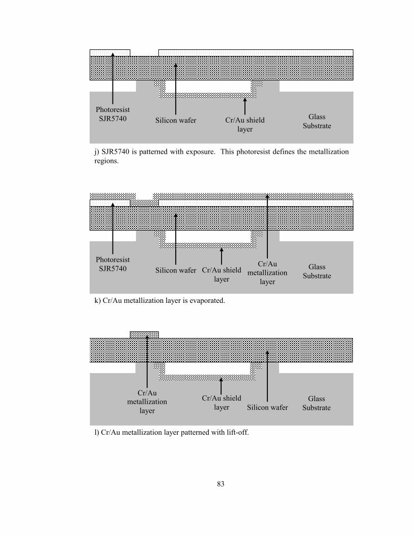
83
j) SJR5740 is patterned with exposure. This photoresist defines the metallization regions.
k) Cr/Au metallization layer is evaporated.
l) Cr/Au metallization layer patterned with lift-off.
Glass Substrate
Cr/Au shield layer
Silicon wafer Photoresist SJR5740
Glass Substrate
Cr/Au shield layer
Silicon wafer Photoresist SJR5740 Cr/Au
metallization layer
Glass Substrate
Cr/Au metallization
layer Cr/Au shield
layer Silicon wafer
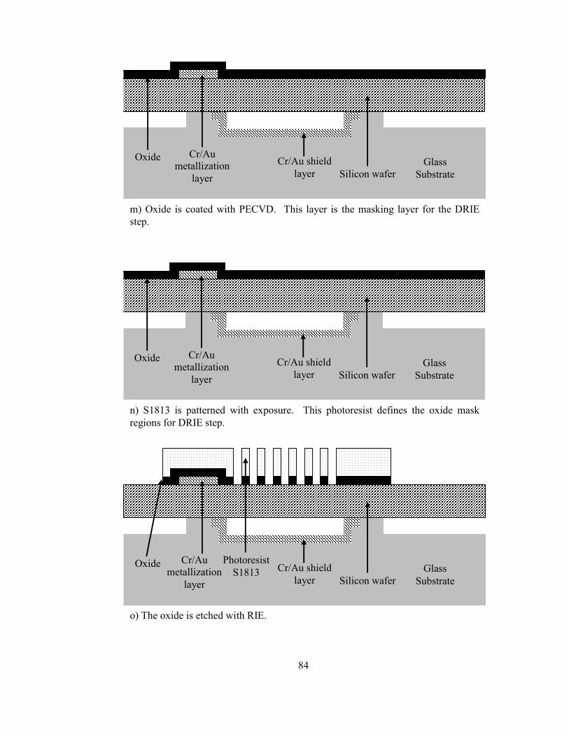
84
m) Oxide is coated with PECVD. This layer is the masking layer for the DRIE step.
n) S1813 is patterned with exposure. This photoresist defines the oxide mask regions for DRIE step.
o) The oxide is etched with RIE.
Glass Substrate
Cr/Au metallization
layer Cr/Au shield
layer Silicon wafer Oxide
Glass Substrate
Cr/Au metallization
layer
Cr/Au shield layer Silicon wafer
Oxide
Glass Substrate
Cr/Au metallization
layer Cr/Au shield
layer Silicon wafer Oxide Photoresist
S1813
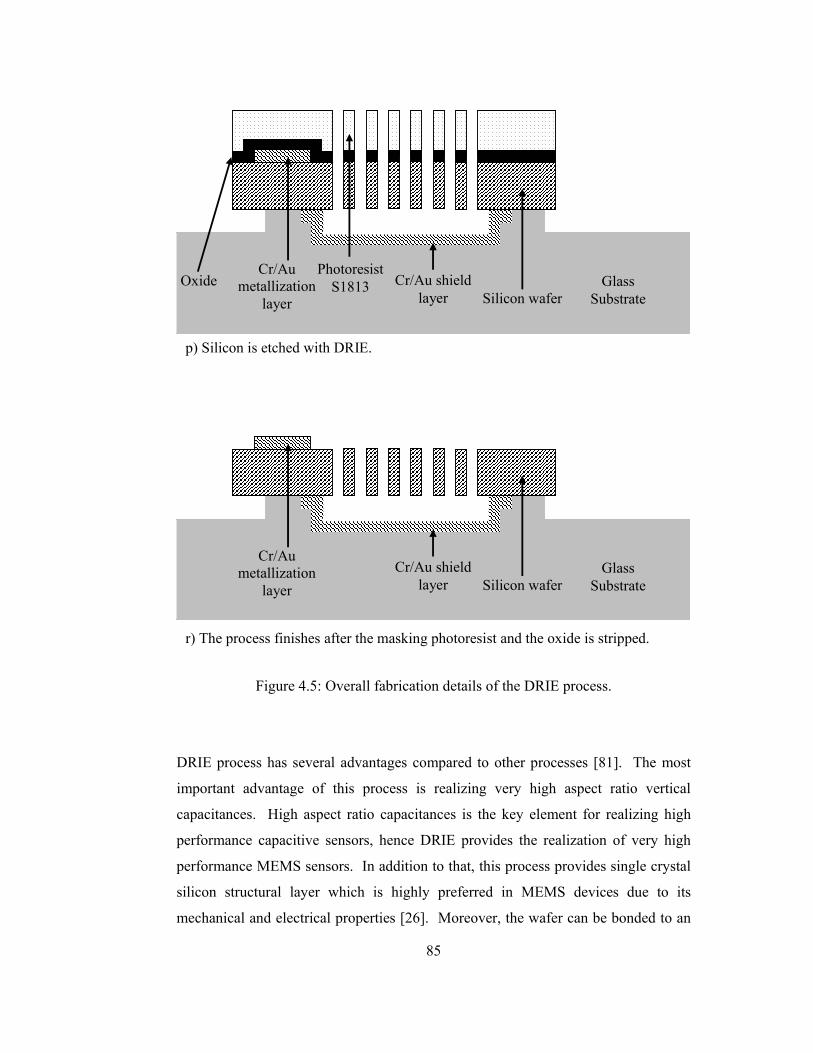
85
p) Silicon is etched with DRIE.
r) The process finishes after the masking photoresist and the oxide is stripped.
Glass Substrate
Cr/Au metallization
layer Cr/Au shield
layer Silicon wafer Oxide
Photoresist S1813
Glass Substrate
Cr/Au metallization
layer Cr/Au shield
layer Silicon wafer
Figure 4.5: Overall fabrication details of the DRIE process.
DRIE process has several advantages compared to other processes [81]. The most
important advantage of this process is realizing very high aspect ratio vertical
capacitances. High aspect ratio capacitances is the key element for realizing high
performance capacitive sensors, hence DRIE provides the realization of very high
performance MEMS sensors. In addition to that, this process provides single crystal
silicon structural layer which is highly preferred in MEMS devices due to its
mechanical and electrical properties [26]. Moreover, the wafer can be bonded to an
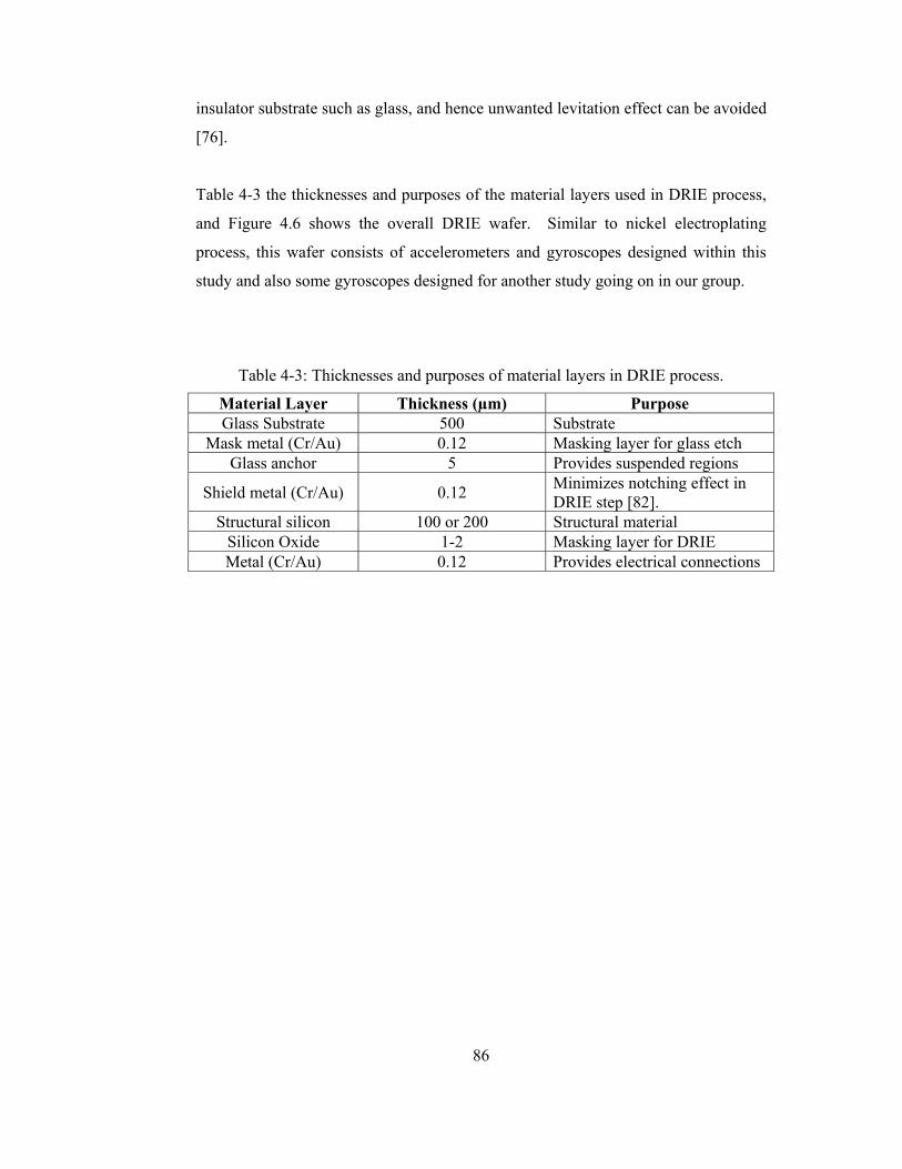
86
insulator substrate such as glass, and hence unwanted levitation effect can be avoided
[76].
Table 4-3 the thicknesses and purposes of the material layers used in DRIE process,
and Figure 4.6 shows the overall DRIE wafer. Similar to nickel electroplating
process, this wafer consists of accelerometers and gyroscopes designed within this
study and also some gyroscopes designed for another study going on in our group.
Table 4-3: Thicknesses and purposes of material layers in DRIE process.
Material Layer Thickness (µm) Purpose Glass Substrate 500 Substrate
Mask metal (Cr/Au) 0.12 Masking layer for glass etch Glass anchor 5 Provides suspended regions
Shield metal (Cr/Au) 0.12 Minimizes notching effect in DRIE step [82].
Structural silicon 100 or 200 Structural material Silicon Oxide 1-2 Masking layer for DRIE Metal (Cr/Au) 0.12 Provides electrical connections
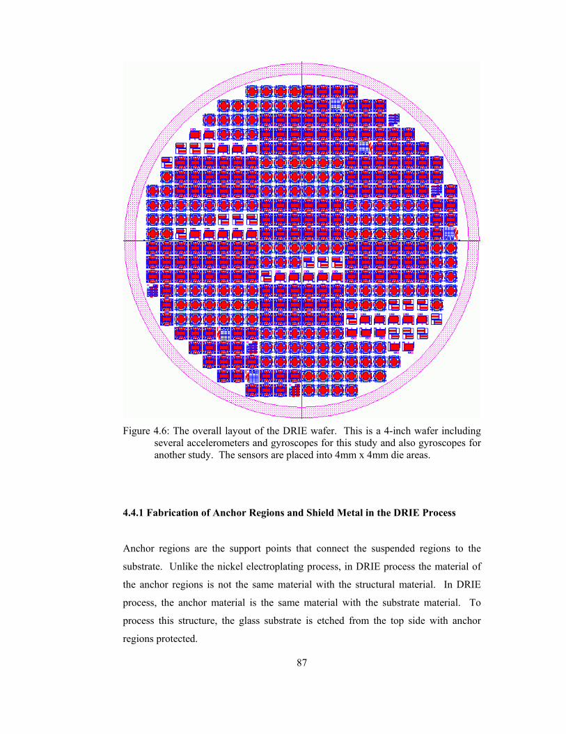
87
Figure 4.6: The overall layout of the DRIE wafer. This is a 4-inch wafer including
several accelerometers and gyroscopes for this study and also gyroscopes for another study. The sensors are placed into 4mm x 4mm die areas.
4.4.1 Fabrication of Anchor Regions and Shield Metal in the DRIE Process
Anchor regions are the support points that connect the suspended regions to the
substrate. Unlike the nickel electroplating process, in DRIE process the material of
the anchor regions is not the same material with the structural material. In DRIE
process, the anchor material is the same material with the substrate material. To
process this structure, the glass substrate is etched from the top side with anchor
regions protected.
88
The anchor region formation is the first process step and hence the process starts
with the preparation of the glass wafer. Similarly with the nickel electroplating
process, the wafer is first put into piranha etchant (1:1 H2SO4:H2O2) for 15 min for
organic cleaning. After this step, the wafer is dipped into BHF (Buffered HF, 6:1
NH4:HF) for 30 sec to increase the adhesion of chromium to the glass substrate. The
masking layer for the glass etch is the evaporated chromium/gold, hence BHF step is
critical. After chromium/gold evaporation (200 Å / 1000 Å) (Figure 4.5 (a))
maN-440 negative resist is patterned with exposure. This patterned photoresist
defines the masking region of the metal mask underneath (Figure 4.5 (b)).
The wafer is dip into gold etchant and then chromium etchant. After these etching
steps the masking metal layer is formed. Then without stripping the photoresist,
using both photoresist and the metal as the masking layer the glass etch process is
done (Figure 4.5 (c)). The glass etchant (10:7:3 DI H2O:HF:HNO3) creates a very
large undercut, decreasing the actual anchor region, but we have considered this
undercut in the design period. After glass etch, the photoresist, the masking gold,
and the masking chromium is stripped (Figure 4.5 (d)).
The next step is the formation of shield metal. The shield metal minimizes the
undesired notching effect in DRIE process [82]. The shield metal should be
electrically connected to the structures and during the DRIE step, the ions that etches
though the silicon will not etch under the silicon afterwards but will bombard the
shield metal layer [82]. Hence, the shield metal should touch the structural silicon in
the anchor points. This can be realized with a thin metal layer placed onto the anchor
points. During the anodic bonding, the silicon can touch the shield layer in these
regions. However, this thin layer will decrease the bonding region, and also will
create a level difference that will further decrease the bonding area. Hence, in the
process flow, we first create a shallow etch region for the shield layer to decrease the
level difference. First, S1828 is patterned with exposure (Figure 4.5 (e)). This
photoresist is the masking layer for shallow glass etch and also enables shield metal
patterning with lift-off. After patterning the photoresist, the wafer is dipped into
BHF (Buffered HF, 6:1 NH4:HF) for the shallow glass etch (Figure 4.5 (f)). Then
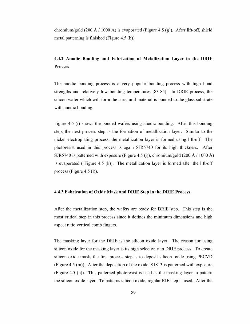
89
chromium/gold (200 Å / 1000 Å) is evaporated (Figure 4.5 (g)). After lift-off, shield
metal patterning is finished (Figure 4.5 (h)).
4.4.2 Anodic Bonding and Fabrication of Metallization Layer in the DRIE
Process
The anodic bonding process is a very popular bonding process with high bond
strengths and relatively low bonding temperatures [83-85]. In DRIE process, the
silicon wafer which will form the structural material is bonded to the glass substrate
with anodic bonding.
Figure 4.5 (i) shows the bonded wafers using anodic bonding. After this bonding
step, the next process step is the formation of metallization layer. Similar to the
nickel electroplating process, the metallization layer is formed using lift-off. The
photoresist used in this process is again SJR5740 for its high thickness. After
SJR5740 is patterned with exposure (Figure 4.5 (j)), chromium/gold (200 Å / 1000 Å)
is evaporated ( Figure 4.5 (k)). The metallization layer is formed after the lift-off
process (Figure 4.5 (l)).
4.4.3 Fabrication of Oxide Mask and DRIE Step in the DRIE Process
After the metallization step, the wafers are ready for DRIE step. This step is the
most critical step in this process since it defines the minimum dimensions and high
aspect ratio vertical comb fingers.
The masking layer for the DRIE is the silicon oxide layer. The reason for using
silicon oxide for the masking layer is its high selectivity in DRIE process. To create
silicon oxide mask, the first process step is to deposit silicon oxide using PECVD
(Figure 4.5 (m)). After the deposition of the oxide, S1813 is patterned with exposure
(Figure 4.5 (n)). This patterned photoresist is used as the masking layer to pattern
the silicon oxide layer. To patterns silicon oxide, regular RIE step is used. After the
90
RIE step (Figure 4.5 (o)), DRIE etching is done using both the oxide layer and the
photoresist as the masking layer (Figure 4.5 (p)). The process ends with stripping
masking photoresist and oxide layers (Figure 4.5 (r)).
Similar to the nickel electroplating process, the dicing issue is also important in
DRIE process. After DRIE step, the wafers are coated with a protective photoresist
before the dicing process and then the dicing is performed. After the dicing, the
protective photoresist is removed sample by sample.
The process steps in this process have already been completed at METU-MET
facilities, except the DRIE step. The DRIE step has been done at STS, one of the
producers of the DRIE machine. A DRIE machine is already purchased from STS
and the installation of it was in progress during the writing of this thesis.
4.5 Summary
This chapter presents the fabrication processes and the details of these processes for
the realization of MEMS accelerometers and gyroscopes. The processes used in this
study are SOIMUMPs process, nickel electroplating process, and DRIE process.
SOIMUMPs process is a commercial MUMPs (Multi-User MEMS Processes)
process which uses SOI wafers and pattern the top silicon layer for the structural
material. This process is realized by CRONOS Inc. Nickel electroplating process is
a surface micromachining process which creates nickel electroplated structures on
top of the glass wafer. All the process steps of this process are realized in
METU-MET facilities. The DRIE process is an advanced process that uses dry
anisotropic bulk micromachining technique. The structural material is silicon and
the substrate is glass. The glass substrate is bonded to silicon wafer using anodic
bonding and then the silicon wafer is etched with DRIE for structural layer formation.
All the process steps, except masking oxide formation and DRIE step, are realized in
METU-MET facilities.
91
CHAPTER 5
FABRICATION AND TEST RESULTS
This chapter presents the fabrication and test results of designed accelerometers and
gyroscopes. The chapter also gives the test results of the accelerometers hybrid
connected to a readout circuit to achieve accelerometer systems. Section 5.1 briefly
discusses the fabrication results of each three fabrication processes. Section 5.2
explains the basic tests done to each accelerometer and gyroscope sample and
summarizes these test results. Section 5.3 gives the open loop test results of hybrid
connected accelerometer prototypes using SOIMUMPs accelerometer and nickel
electroplated accelerometer with MS3110 commercial capacitive readout circuit.
Finally, Section 5.4 summarizes the chapter and discusses the test results.
5.1 Fabrication Results of Each Three Processes
This section explains the fabrication results of each three processes. Our first
process is SOIMUMPs process which is fabricated by CRONOS Inc. The devices
are designed and sent for fabrication in CRONOS fabrication facilities. The second
process is nickel electroplating process, which is realized in METU-MET facilities.
The last process is the DRIE process. The fabrication steps of this process are also
realized in METU-MET facilities except the oxide formation and DRIE etching steps.
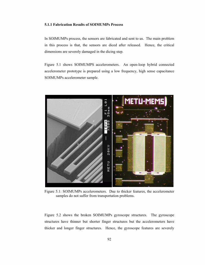
92
5.1.1 Fabrication Results of SOIMUMPs Process
In SOIMUMPs process, the sensors are fabricated and sent to us. The main problem
in this process is that, the sensors are diced after released. Hence, the critical
dimensions are severely damaged in the dicing step.
Figure 5.1 shows SOIMUMPS accelerometers. An open-loop hybrid connected
accelerometer prototype is prepared using a low frequency, high sense capacitance
SOIMUMPs accelerometer sample.
Figure 5.1: SOIMUMPs accelerometers. Due to thicker features, the accelerometer
samples do not suffer from transportation problems.
Figure 5.2 shows the broken SOIMUMPs gyroscope structures. The gyroscope
structures have thinner but shorter finger structures but the accelerometers have
thicker and longer finger structures. Hence, the gyroscope features are severely
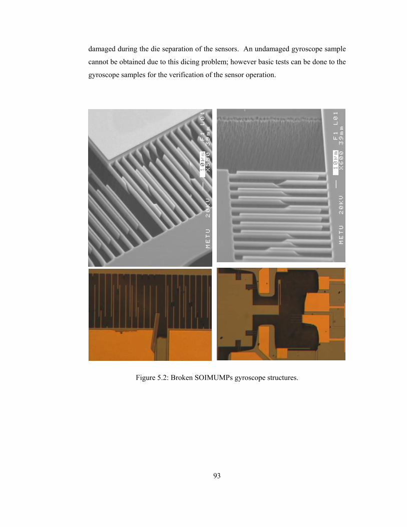
93
damaged during the die separation of the sensors. An undamaged gyroscope sample
cannot be obtained due to this dicing problem; however basic tests can be done to the
gyroscope samples for the verification of the sensor operation.
Figure 5.2: Broken SOIMUMPs gyroscope structures.
94
5.1.2 Fabrication Results Nickel Electroplating Process
The nickel electroplating process results have turned out to be the most expected
fabrication results. In the design period, we have expected that the mold photoresist
will shrink in each direction during the exposure; hence the electroplated region area
will increase. So, we compensate this shrinking of the mold photoresist in our design
drawings. As expected, the mold photoresist shrink in each direction during the
exposure, hence the electroplated area increase during the fabrication. Hence we
have achieved designed resonance frequency values for our sensors. We have also
expected that during the hardbake of the mold photoresist, the shape of the
photoresist will change, especially in the bulky regions. This deformation in the
shape is also observed after the fabrication, especially near the spring regions of the
accelerometers. We expect that this deformation will cause drift in the accelerometer
system and will also change the resonance frequency of the accelerometer, but the
hardbake part is critical due to the fact that the photoresist cannot withstand the
electroplating solution without the hardbake. Moreover, we expect that the
uniformity of the electroplating thickness will not be perfect, and hence there will be
height difference throughout the wafer. The fabricated samples also verify our
expectations.
Figure 5.3 shows a fabricated nickel electroplated accelerometer sample and shows
the deformation in the spring regions. Figure 5.4 shows the SEM pictures of
accelerometer samples. A hybrid connected accelerometer prototype is formed using
a high performance fabricated accelerometers.
Figure 5.5 shows a fabricated nickel electroplated gyroscope. The operation of the
gyroscopes is verified with basic tests that will be explained in Section 5.2.

95
Deformation in the spring regions
Figure 5.3: A fabricated nickel electroplated accelerometer and the deformation in the spring regions.
Figure 5.4: SEM pictures of fabricated nickel electroplated accelerometers.

96
Figure 5.5: A photograph of fabricated nickel electroplated gyroscope.
5.1.3 Fabrication Results of DRIE Process
The DRIE process results show that this process still needs optimization. The DRIE
etch step is the most critical step in this process and it seems that we have lost all our
samples during this step. The wide openings of the samples are etched away with a
faster etch rate and then while the smaller opening regions are being etched, there
occurs large under etches in the wide opening regions, or in the small opening
regions the etching is not finished. These are the main problems in DRIE process.
Figure 5.6 shows a SEM picture of a DRIE gyroscope. The fabrication of this
gyroscope seems to be good; however the gyroscope still suffers from the DRIE
fabrication problems. Figure 5.7 shows SEM pictures of DRIE samples, and the
problematic regions are better seen from this picture. In this figure, it can be shown
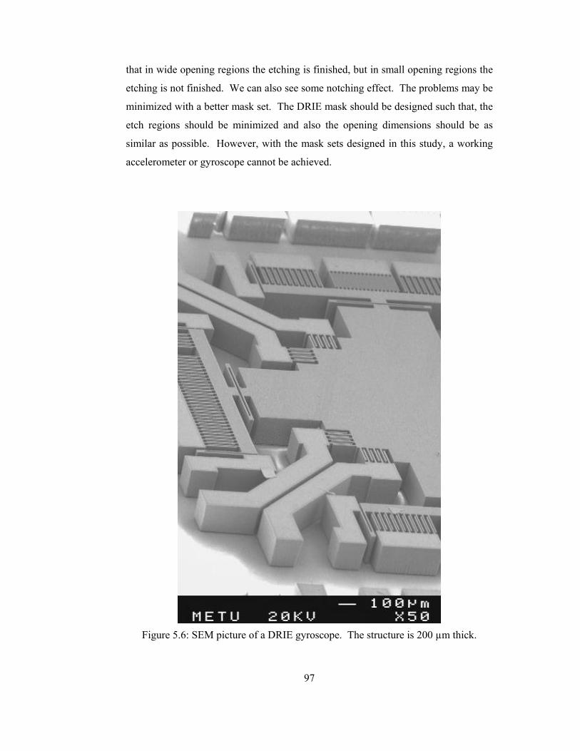
97
that in wide opening regions the etching is finished, but in small opening regions the
etching is not finished. We can also see some notching effect. The problems may be
minimized with a better mask set. The DRIE mask should be designed such that, the
etch regions should be minimized and also the opening dimensions should be as
similar as possible. However, with the mask sets designed in this study, a working
accelerometer or gyroscope cannot be achieved.
Figure 5.6: SEM picture of a DRIE gyroscope. The structure is 200 µm thick.
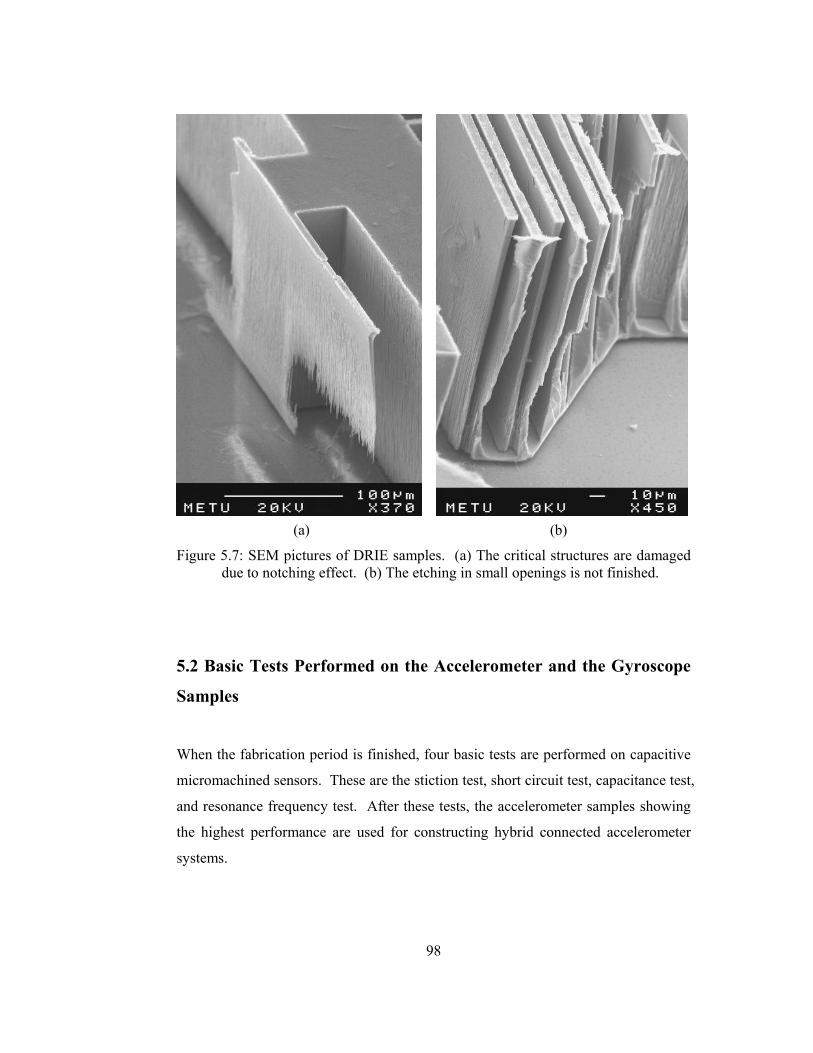
98
(a) (b) Figure 5.7: SEM pictures of DRIE samples. (a) The critical structures are damaged
due to notching effect. (b) The etching in small openings is not finished.
5.2 Basic Tests Performed on the Accelerometer and the Gyroscope
Samples
When the fabrication period is finished, four basic tests are performed on capacitive
micromachined sensors. These are the stiction test, short circuit test, capacitance test,
and resonance frequency test. After these tests, the accelerometer samples showing
the highest performance are used for constructing hybrid connected accelerometer
systems.
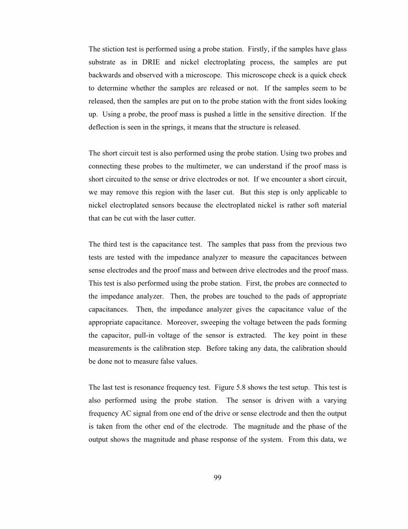
99
The stiction test is performed using a probe station. Firstly, if the samples have glass
substrate as in DRIE and nickel electroplating process, the samples are put
backwards and observed with a microscope. This microscope check is a quick check
to determine whether the samples are released or not. If the samples seem to be
released, then the samples are put on to the probe station with the front sides looking
up. Using a probe, the proof mass is pushed a little in the sensitive direction. If the
deflection is seen in the springs, it means that the structure is released.
The short circuit test is also performed using the probe station. Using two probes and
connecting these probes to the multimeter, we can understand if the proof mass is
short circuited to the sense or drive electrodes or not. If we encounter a short circuit,
we may remove this region with the laser cut. But this step is only applicable to
nickel electroplated sensors because the electroplated nickel is rather soft material
that can be cut with the laser cutter.
The third test is the capacitance test. The samples that pass from the previous two
tests are tested with the impedance analyzer to measure the capacitances between
sense electrodes and the proof mass and between drive electrodes and the proof mass.
This test is also performed using the probe station. First, the probes are connected to
the impedance analyzer. Then, the probes are touched to the pads of appropriate
capacitances. Then, the impedance analyzer gives the capacitance value of the
appropriate capacitance. Moreover, sweeping the voltage between the pads forming
the capacitor, pull-in voltage of the sensor is extracted. The key point in these
measurements is the calibration step. Before taking any data, the calibration should
be done not to measure false values.
The last test is resonance frequency test. Figure 5.8 shows the test setup. This test is
also performed using the probe station. The sensor is driven with a varying
frequency AC signal from one end of the drive or sense electrode and then the output
is taken from the other end of the electrode. The magnitude and the phase of the
output shows the magnitude and phase response of the system. From this data, we

100
can see that the peak value of the magnitude response, which corresponds to the
resonance frequency of the sensor.
NetworkAnalyzer
ProofMass OutputAC input
DC Bias Figure 5.8: Resonance frequency test setup.
For SOIMUMPs and nickel electroplating process, capacitance and resonance
frequency tests can be performed, but for DRIE process, there is not any testable
sensor for these tests.
Figure 5.9-16 show the capacitance test results of each sensor. The capacitance
between the proof mass and the sense electrode increases with the applied voltage
across them. Hence, after the pull-in voltage, the proof mass sticks to the sense
electrode. Table 5-1 compares the designed pull-in voltages with the measured
values.
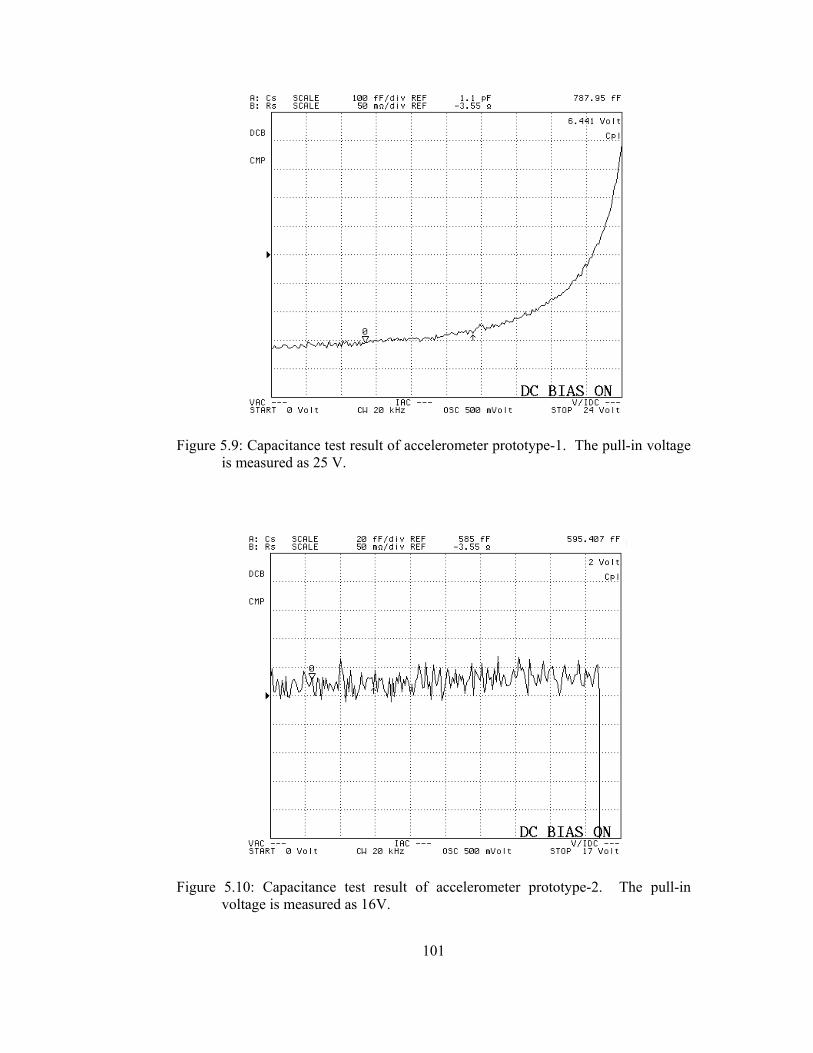
101
Figure 5.9: Capacitance test result of accelerometer prototype-1. The pull-in voltage is measured as 25 V.
Figure 5.10: Capacitance test result of accelerometer prototype-2. The pull-in voltage is measured as 16V.
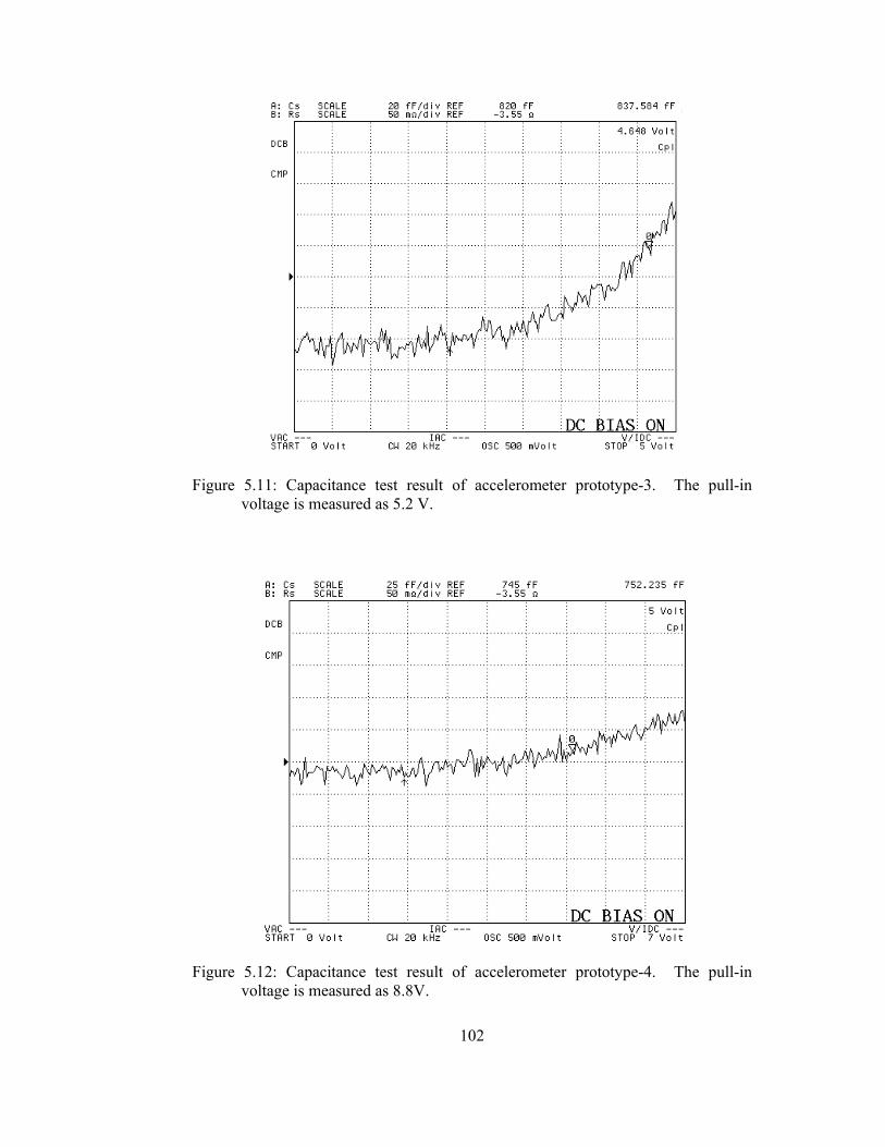
102
Figure 5.11: Capacitance test result of accelerometer prototype-3. The pull-in voltage is measured as 5.2 V.
Figure 5.12: Capacitance test result of accelerometer prototype-4. The pull-in voltage is measured as 8.8V.
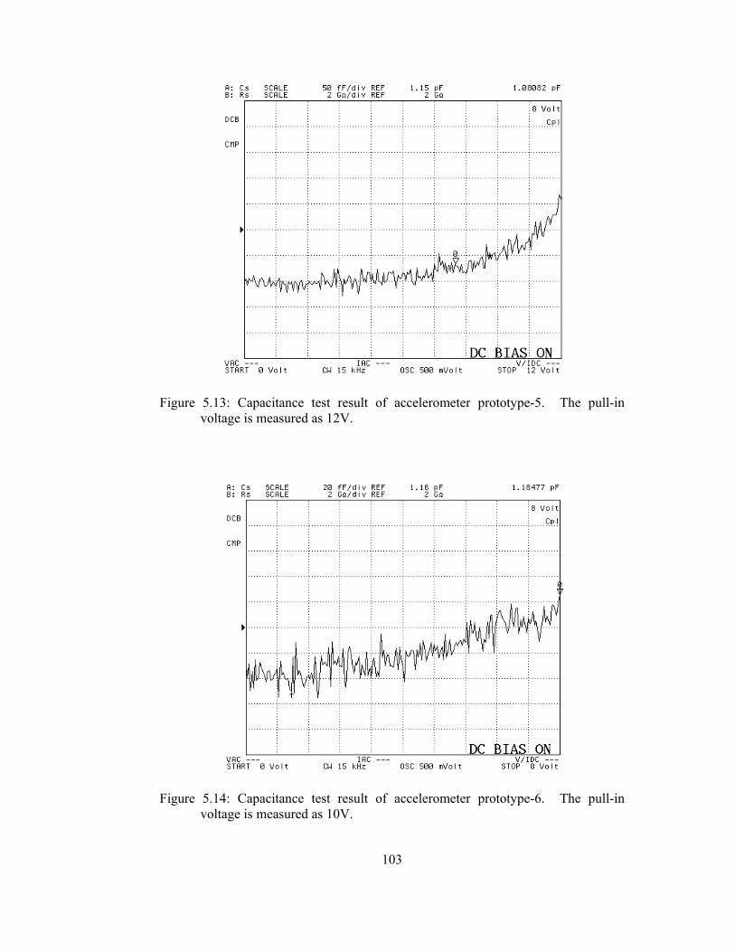
103
Figure 5.13: Capacitance test result of accelerometer prototype-5. The pull-in voltage is measured as 12V.
Figure 5.14: Capacitance test result of accelerometer prototype-6. The pull-in voltage is measured as 10V.
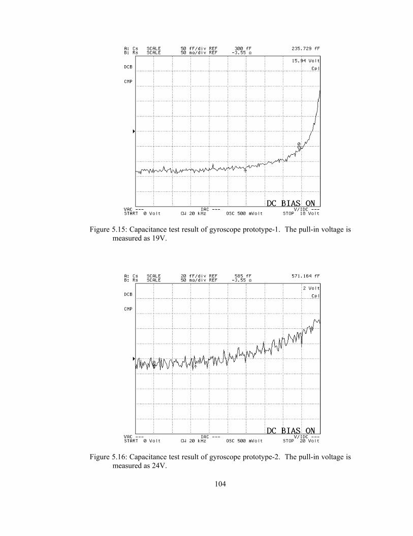
104
Figure 5.15: Capacitance test result of gyroscope prototype-1. The pull-in voltage is measured as 19V.
Figure 5.16: Capacitance test result of gyroscope prototype-2. The pull-in voltage is measured as 24V.
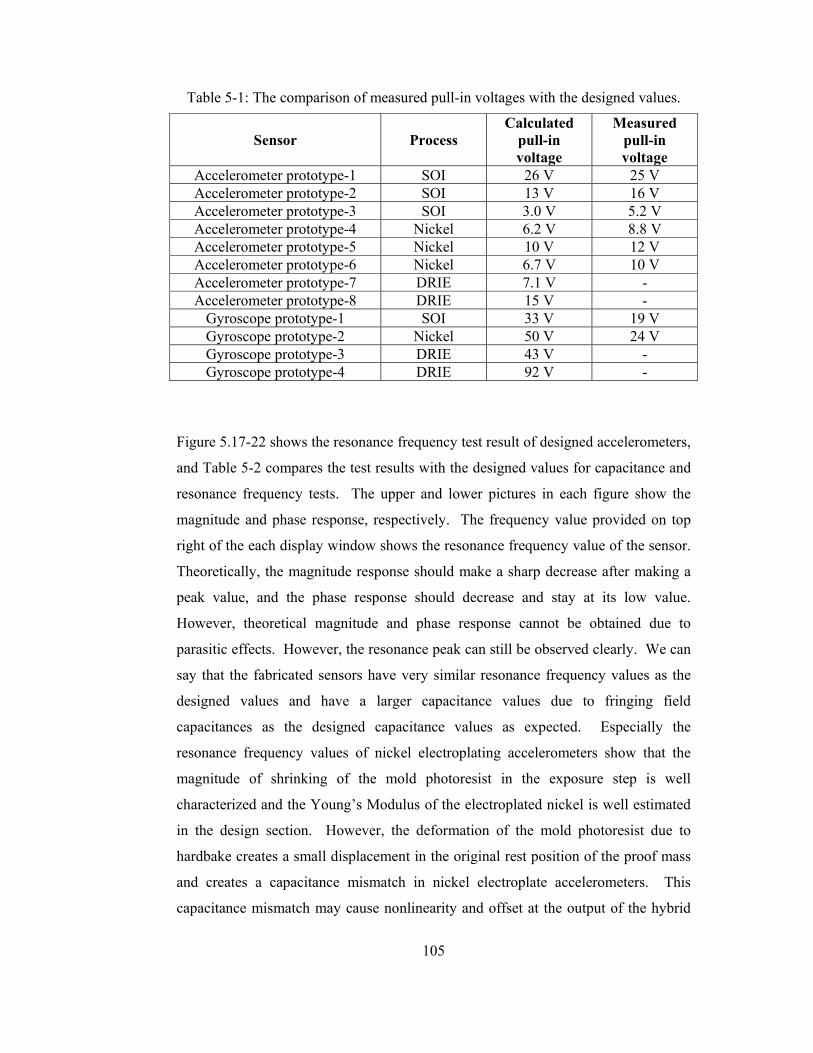
105
Table 5-1: The comparison of measured pull-in voltages with the designed values.
Sensor Process Calculated
pull-in voltage
Measured pull-in voltage
Accelerometer prototype-1 SOI 26 V 25 V Accelerometer prototype-2 SOI 13 V 16 V Accelerometer prototype-3 SOI 3.0 V 5.2 V Accelerometer prototype-4 Nickel 6.2 V 8.8 V Accelerometer prototype-5 Nickel 10 V 12 V Accelerometer prototype-6 Nickel 6.7 V 10 V Accelerometer prototype-7 DRIE 7.1 V - Accelerometer prototype-8 DRIE 15 V -
Gyroscope prototype-1 SOI 33 V 19 V Gyroscope prototype-2 Nickel 50 V 24 V Gyroscope prototype-3 DRIE 43 V - Gyroscope prototype-4 DRIE 92 V -
Figure 5.17-22 shows the resonance frequency test result of designed accelerometers,
and Table 5-2 compares the test results with the designed values for capacitance and
resonance frequency tests. The upper and lower pictures in each figure show the
magnitude and phase response, respectively. The frequency value provided on top
right of the each display window shows the resonance frequency value of the sensor.
Theoretically, the magnitude response should make a sharp decrease after making a
peak value, and the phase response should decrease and stay at its low value.
However, theoretical magnitude and phase response cannot be obtained due to
parasitic effects. However, the resonance peak can still be observed clearly. We can
say that the fabricated sensors have very similar resonance frequency values as the
designed values and have a larger capacitance values due to fringing field
capacitances as the designed capacitance values as expected. Especially the
resonance frequency values of nickel electroplating accelerometers show that the
magnitude of shrinking of the mold photoresist in the exposure step is well
characterized and the Young’s Modulus of the electroplated nickel is well estimated
in the design section. However, the deformation of the mold photoresist due to
hardbake creates a small displacement in the original rest position of the proof mass
and creates a capacitance mismatch in nickel electroplate accelerometers. This
capacitance mismatch may cause nonlinearity and offset at the output of the hybrid

106
connected accelerometer system because proof mass displacement due to external
acceleration will not create a symmetric capacitance difference for same magnitude,
different direction acceleration inputs. Considering the bandwidth issue and these
tests results, prototype-3 and prototype-5 are selected as the sensor element for the
hybrid connected accelerometer system prototypes.
Figure 5.17: Resonance frequency test result of accelerometer prototype-1. The
measured resonance frequency is 31.3 kHz. The upper and lower pictures show the magnitude and phase response, respectively. The frequency value shown on top right of the each display window shows the resonance frequency value of the sensor. Theoretically, the magnitude response should make a sharp decrease after making a peak value, and the phase response should decrease and stay at its low value. However, due to parasitic effects theoretical results cannot be obtained.
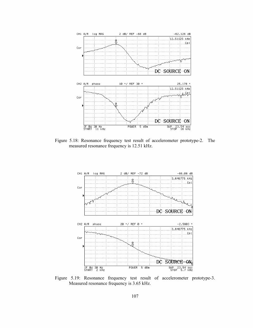
107
Figure 5.18: Resonance frequency test result of accelerometer prototype-2. The
measured resonance frequency is 12.51 kHz.
Figure 5.19: Resonance frequency test result of accelerometer prototype-3.
Measured resonance frequency is 3.65 kHz.

108
Figure 5.20: Resonance frequency test result of accelerometer prototype-4.
Measured resonance frequency is 2.55 kHz.
Figure 5.21: Resonance frequency test result of accelerometer prototype-5.
Measured resonance frequency is 2.09 kHz.
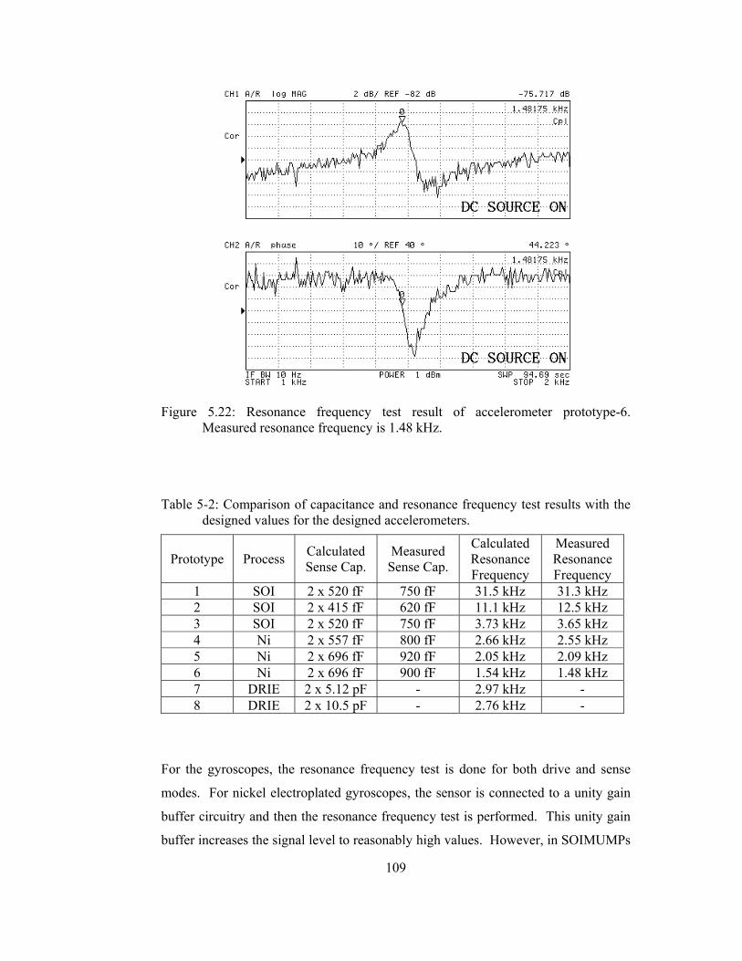
109
Figure 5.22: Resonance frequency test result of accelerometer prototype-6.
Measured resonance frequency is 1.48 kHz.
Table 5-2: Comparison of capacitance and resonance frequency test results with the designed values for the designed accelerometers.
Prototype Process Calculated Sense Cap.
Measured Sense Cap.
Calculated Resonance Frequency
Measured Resonance Frequency
1 SOI 2 x 520 fF 750 fF 31.5 kHz 31.3 kHz 2 SOI 2 x 415 fF 620 fF 11.1 kHz 12.5 kHz 3 SOI 2 x 520 fF 750 fF 3.73 kHz 3.65 kHz 4 Ni 2 x 557 fF 800 fF 2.66 kHz 2.55 kHz 5 Ni 2 x 696 fF 920 fF 2.05 kHz 2.09 kHz 6 Ni 2 x 696 fF 900 fF 1.54 kHz 1.48 kHz 7 DRIE 2 x 5.12 pF - 2.97 kHz - 8 DRIE 2 x 10.5 pF - 2.76 kHz -
For the gyroscopes, the resonance frequency test is done for both drive and sense
modes. For nickel electroplated gyroscopes, the sensor is connected to a unity gain
buffer circuitry and then the resonance frequency test is performed. This unity gain
buffer increases the signal level to reasonably high values. However, in SOIMUMPs
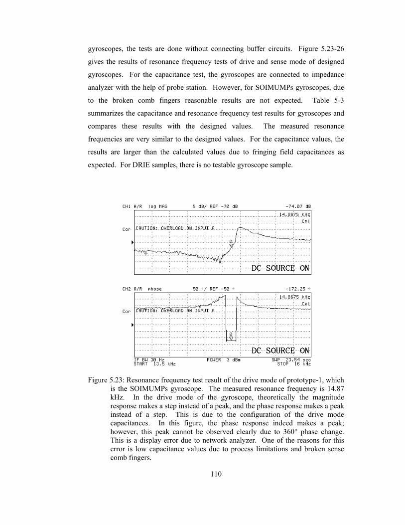
110
gyroscopes, the tests are done without connecting buffer circuits. Figure 5.23-26
gives the results of resonance frequency tests of drive and sense mode of designed
gyroscopes. For the capacitance test, the gyroscopes are connected to impedance
analyzer with the help of probe station. However, for SOIMUMPs gyroscopes, due
to the broken comb fingers reasonable results are not expected. Table 5-3
summarizes the capacitance and resonance frequency test results for gyroscopes and
compares these results with the designed values. The measured resonance
frequencies are very similar to the designed values. For the capacitance values, the
results are larger than the calculated values due to fringing field capacitances as
expected. For DRIE samples, there is no testable gyroscope sample.
Figure 5.23: Resonance frequency test result of the drive mode of prototype-1, which
is the SOIMUMPs gyroscope. The measured resonance frequency is 14.87 kHz. In the drive mode of the gyroscope, theoretically the magnitude response makes a step instead of a peak, and the phase response makes a peak instead of a step. This is due to the configuration of the drive mode capacitances. In this figure, the phase response indeed makes a peak; however, this peak cannot be observed clearly due to 360° phase change. This is a display error due to network analyzer. One of the reasons for this error is low capacitance values due to process limitations and broken sense comb fingers.
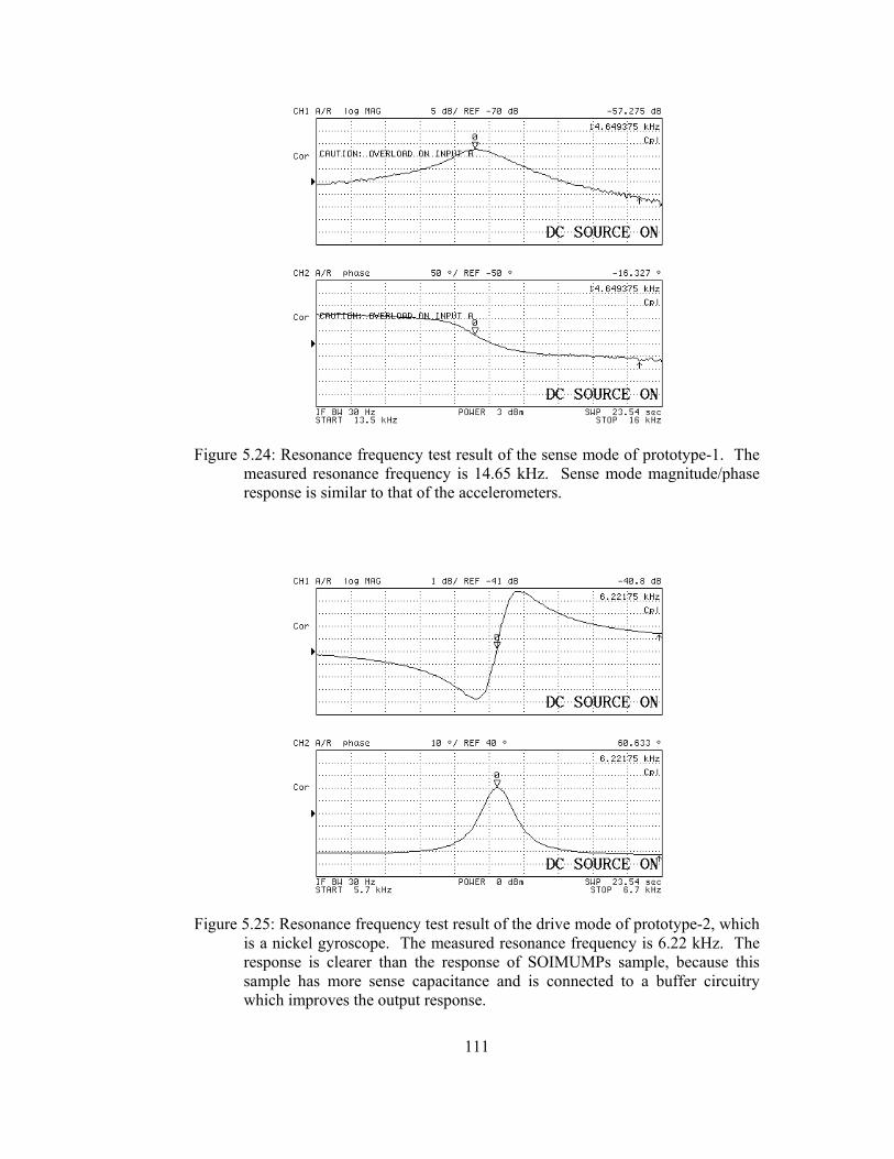
111
Figure 5.24: Resonance frequency test result of the sense mode of prototype-1. The
measured resonance frequency is 14.65 kHz. Sense mode magnitude/phase response is similar to that of the accelerometers.
Figure 5.25: Resonance frequency test result of the drive mode of prototype-2, which
is a nickel gyroscope. The measured resonance frequency is 6.22 kHz. The response is clearer than the response of SOIMUMPs sample, because this sample has more sense capacitance and is connected to a buffer circuitry which improves the output response.
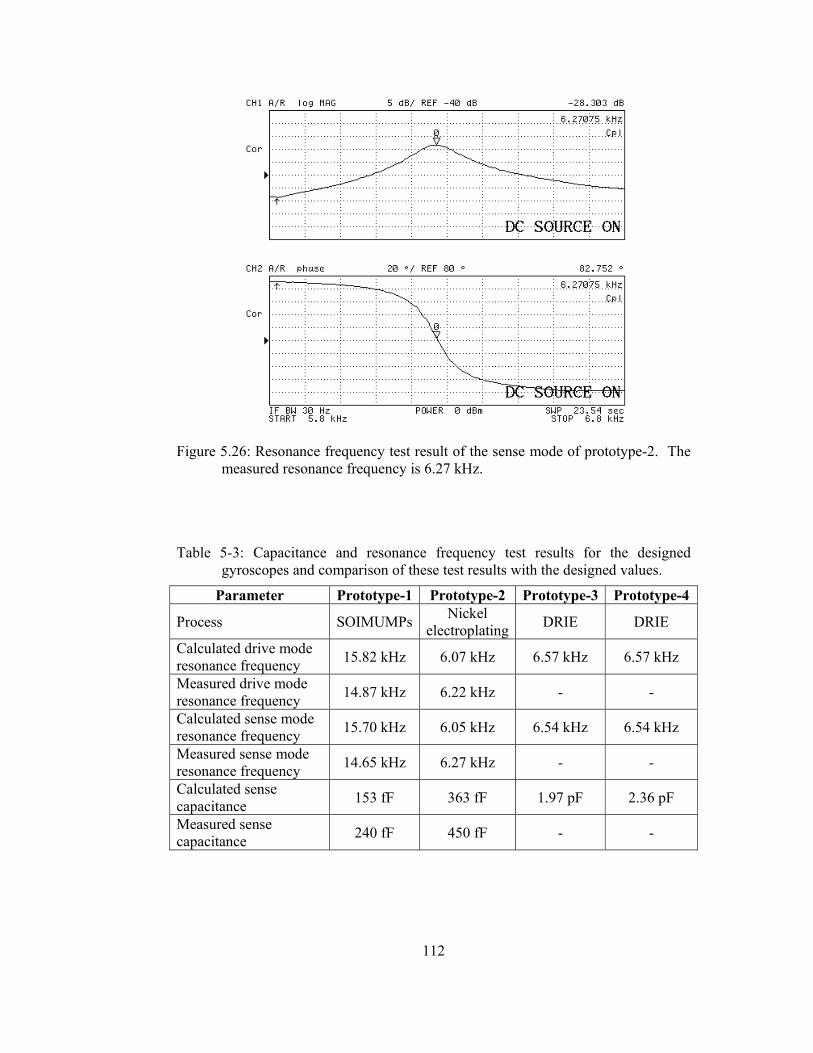
112
Figure 5.26: Resonance frequency test result of the sense mode of prototype-2. The
measured resonance frequency is 6.27 kHz.
Table 5-3: Capacitance and resonance frequency test results for the designed gyroscopes and comparison of these test results with the designed values.
Parameter Prototype-1 Prototype-2 Prototype-3 Prototype-4
Process SOIMUMPs Nickel electroplating DRIE DRIE
Calculated drive mode resonance frequency 15.82 kHz 6.07 kHz 6.57 kHz 6.57 kHz
Measured drive mode resonance frequency 14.87 kHz 6.22 kHz - -
Calculated sense mode resonance frequency 15.70 kHz 6.05 kHz 6.54 kHz 6.54 kHz
Measured sense mode resonance frequency 14.65 kHz 6.27 kHz - -
Calculated sense capacitance 153 fF 363 fF 1.97 pF 2.36 pF
Measured sense capacitance 240 fF 450 fF - -

113
5.3 Open Loop Tests of Accelerometers and MS3110 Readout
Circuitry Hybrid System
Accelerometer prototype-3 and prototype-5 are selected for the sensor element of the
hybrid system. The aim of these prototypes is to form an accelerometer system that
satisfies the goals of this study. Hence, the prototypes should have bias circuitries,
sensor part, MS3110 readout part, and amplifier stages that bring the output signal to
desired levels.
Figure 5.27 shows the first generation hybrid accelerometer system that uses
accelerometer prototype-3 and MS3110 readout circuitry, and Figure 5.28 shows the
block diagram of this prototype. MS3110 is a switched-capacitor integrator type
differential open-loop capacitive readout circuit. The circuit generates the clock
signals necessary for the reading of capacitance mismatch due to external
acceleration input, and then converts this capacitance mismatch to voltage with the
help of a switched capacitor integrator. Next, the circuit eliminates high frequency
component of the signal with a Low-Pass-Filter (LPF), and finally amplifies the
resultant signal. The pole of this LPF is 500 Hz, and this pole determines the total
3dB bandwidth of the system, because the 3dB bandwidth of the accelerometer is
nearly its resonance frequency. The bias voltages required for MS3110 circuit, and
amplifier stages to adjust the voltage gain of the system is not provided with the first
generation hybrid system, but these circuitries can be constructed, and the bias
voltages can be supplied externally.
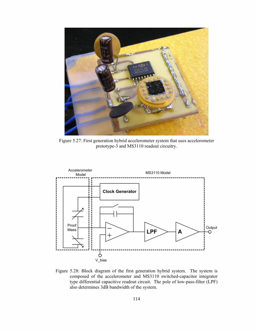
114
Figure 5.27: First generation hybrid accelerometer system that uses accelerometer
prototype-3 and MS3110 readout circuitry.
A
Clock Generator
V_bias
MS3110 ModelAccelerometer
Model
ProofMass Output
LPF
Figure 5.28: Block diagram of the first generation hybrid system. The system is composed of the accelerometer and MS3110 switched-capacitor integrator type differential capacitive readout circuit. The pole of low-pass-filter (LPF) also determines 3dB bandwidth of the system.
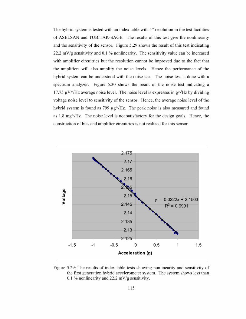
115
The hybrid system is tested with an index table with 1° resolution in the test facilities
of ASELSAN and TUBITAK-SAGE. The results of this test give the nonlinearity
and the sensitivity of the sensor. Figure 5.29 shows the result of this test indicating
22.2 mV/g sensitivity and 0.1 % nonlinearity. The sensitivity value can be increased
with amplifier circuitries but the resolution cannot be improved due to the fact that
the amplifiers will also amplify the noise levels. Hence the performance of the
hybrid system can be understood with the noise test. The noise test is done with a
spectrum analyzer. Figure 5.30 shows the result of the noise test indicating a
17.75 µV/√Hz average noise level. The noise level is expresses in g/√Hz by dividing
voltage noise level to sensitivity of the sensor. Hence, the average noise level of the
hybrid system is found as 799 µg/√Hz. The peak noise is also measured and found
as 1.8 mg/√Hz. The noise level is not satisfactory for the design goals. Hence, the
construction of bias and amplifier circuitries is not realized for this sensor.
y = -0.0222x + 2.1503R2 = 0.9991
2.125
2.13
2.135
2.14
2.145
2.15
2.155
2.16
2.165
2.17
2.175
-1.5 -1 -0.5 0 0.5 1 1.5
Acceleration (g)
Vol
tage
Figure 5.29: The results of index table tests showing nonlinearity and sensitivity of
the first generation hybrid accelerometer system. The system shows less than 0.1 % nonlinearity and 22.2 mV/g sensitivity.

116
Average noise level is found as 17.75 µV/√Hz, which corresponds to 799 µg/√Hz. Peak noise floor is measured as 1.8 mg/√Hz.
Figure 5.30: Noise test result of first generation hybrid accelerometer system. Average noise level is found as 17.75 µV/√Hz which corresponds to 799 µg/√Hz. Peak noise floor is measured as 1.8 mg/√Hz.
Table 5-4 gives the comparison of measured and calculated noise levels of the hybrid
system. The total noise of the system has two components: mechanical and electrical
noise. The theoretical mechanical noise can be calculated using Brownian Noise
expression [26], and the electrical noise estimation can be done checking MS3110
datasheet. However, in the MS3110 datasheet, the electrical noise expression is
given as “Input Capacitance Resolution,” but it is not clear whether this capacitance
resolution is single-ended or differential. Therefore, the calculation of electrical
noise changes if the capacitance resolution provided in MS3110 datasheet is single-
ended or differential. Table 5-4 gives the electrical noise estimation for both single-
ended and differential case. However, the noise simulation results show that the
given capacitance resolution should be single-ended.
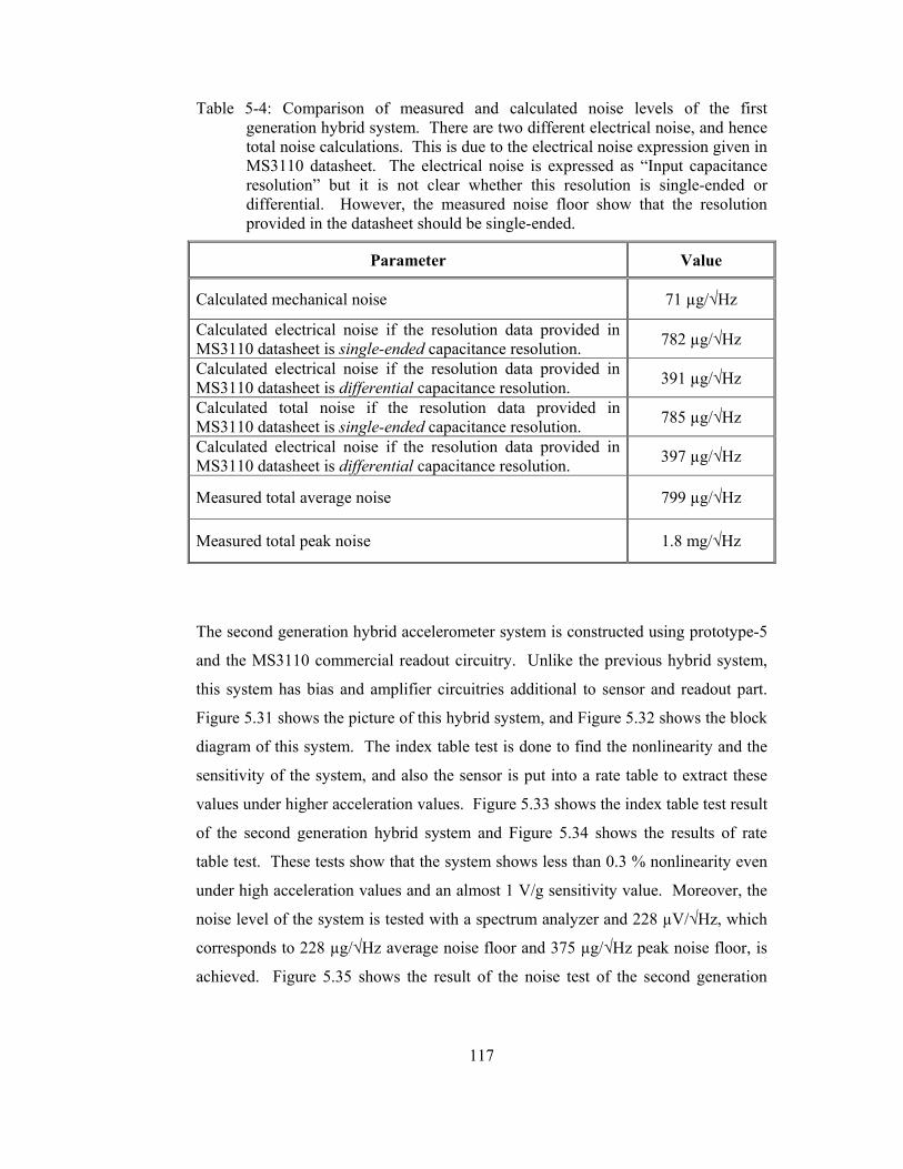
117
Table 5-4: Comparison of measured and calculated noise levels of the first generation hybrid system. There are two different electrical noise, and hence total noise calculations. This is due to the electrical noise expression given in MS3110 datasheet. The electrical noise is expressed as “Input capacitance resolution” but it is not clear whether this resolution is single-ended or differential. However, the measured noise floor show that the resolution provided in the datasheet should be single-ended.
Parameter Value
Calculated mechanical noise 71 µg/√Hz
Calculated electrical noise if the resolution data provided in MS3110 datasheet is single-ended capacitance resolution. 782 µg/√Hz
Calculated electrical noise if the resolution data provided in MS3110 datasheet is differential capacitance resolution. 391 µg/√Hz
Calculated total noise if the resolution data provided in MS3110 datasheet is single-ended capacitance resolution. 785 µg/√Hz
Calculated electrical noise if the resolution data provided in MS3110 datasheet is differential capacitance resolution. 397 µg/√Hz
Measured total average noise 799 µg/√Hz
Measured total peak noise 1.8 mg/√Hz
The second generation hybrid accelerometer system is constructed using prototype-5
and the MS3110 commercial readout circuitry. Unlike the previous hybrid system,
this system has bias and amplifier circuitries additional to sensor and readout part.
Figure 5.31 shows the picture of this hybrid system, and Figure 5.32 shows the block
diagram of this system. The index table test is done to find the nonlinearity and the
sensitivity of the system, and also the sensor is put into a rate table to extract these
values under higher acceleration values. Figure 5.33 shows the index table test result
of the second generation hybrid system and Figure 5.34 shows the results of rate
table test. These tests show that the system shows less than 0.3 % nonlinearity even
under high acceleration values and an almost 1 V/g sensitivity value. Moreover, the
noise level of the system is tested with a spectrum analyzer and 228 µV/√Hz, which
corresponds to 228 µg/√Hz average noise floor and 375 µg/√Hz peak noise floor, is
achieved. Figure 5.35 shows the result of the noise test of the second generation
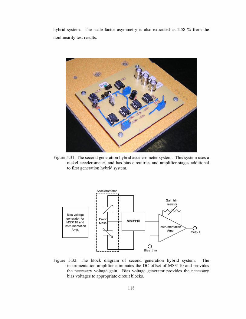
118
hybrid system. The scale factor asymmetry is also extracted as 2.58 % from the
nonlinearity test results.
Figure 5.31: The second generation hybrid accelerometer system. This system uses a
nickel accelerometer, and has bias circuitries and amplifier stages additional to first generation hybrid system.
ProofMass MS3110
Instrumentation Amp.
Bias_trim
Gain trimresistor
Output
Bias voltagegenerator forMS3110 and
InstrumentationAmp.
Accelerometer
Figure 5.32: The block diagram of second generation hybrid system. The instrumentation amplifier eliminates the DC offset of MS3110 and provides the necessary voltage gain. Bias voltage generator provides the necessary bias voltages to appropriate circuit blocks.
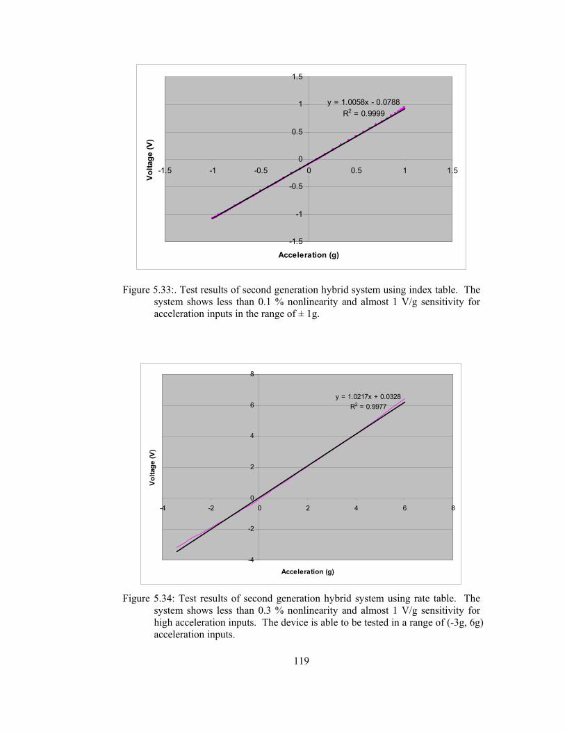
119
y = 1.0058x - 0.0788R2 = 0.9999
-1.5
-1
-0.5
0
0.5
1
1.5
-1.5 -1 -0.5 0 0.5 1 1.5
Acceleration (g)
Volta
ge (V
)
Figure 5.33:. Test results of second generation hybrid system using index table. The system shows less than 0.1 % nonlinearity and almost 1 V/g sensitivity for acceleration inputs in the range of ± 1g.
y = 1.0217x + 0.0328R2 = 0.9977
-4
-2
0
2
4
6
8
-4 -2 0 2 4 6 8
Acceleration (g)
Volta
ge (V
)
Figure 5.34: Test results of second generation hybrid system using rate table. The
system shows less than 0.3 % nonlinearity and almost 1 V/g sensitivity for high acceleration inputs. The device is able to be tested in a range of (-3g, 6g) acceleration inputs.
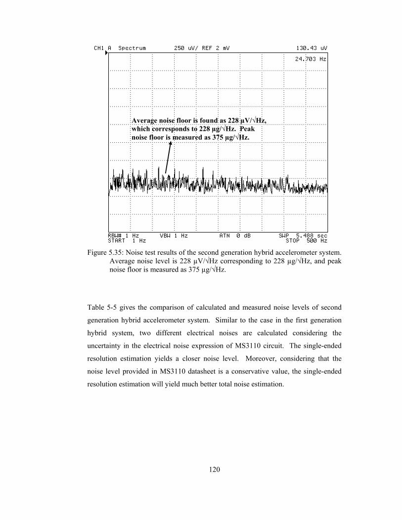
120
Average noise floor is found as 228 µV/√Hz, which corresponds to 228 µg/√Hz. Peak noise floor is measured as 375 µg/√Hz.
Figure 5.35: Noise test results of the second generation hybrid accelerometer system. Average noise level is 228 µV/√Hz corresponding to 228 µg/√Hz, and peak noise floor is measured as 375 µg/√Hz.
Table 5-5 gives the comparison of calculated and measured noise levels of second
generation hybrid accelerometer system. Similar to the case in the first generation
hybrid system, two different electrical noises are calculated considering the
uncertainty in the electrical noise expression of MS3110 circuit. The single-ended
resolution estimation yields a closer noise level. Moreover, considering that the
noise level provided in MS3110 datasheet is a conservative value, the single-ended
resolution estimation will yield much better total noise estimation.
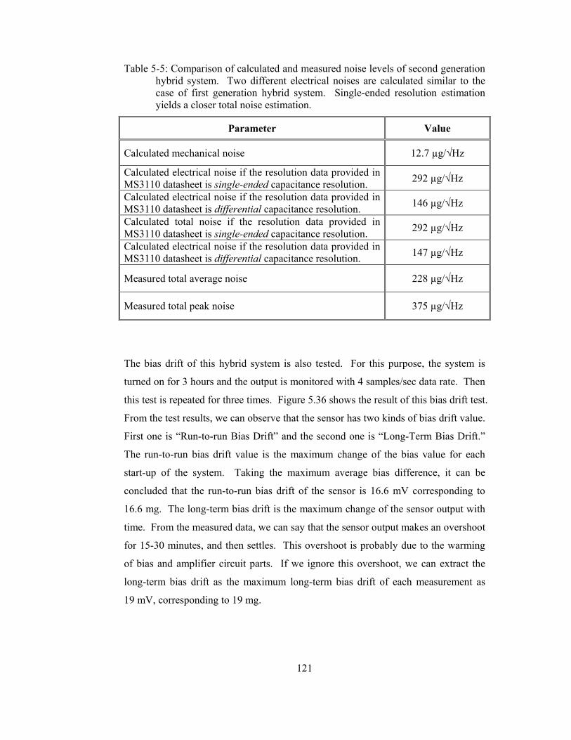
121
Table 5-5: Comparison of calculated and measured noise levels of second generation hybrid system. Two different electrical noises are calculated similar to the case of first generation hybrid system. Single-ended resolution estimation yields a closer total noise estimation.
Parameter Value
Calculated mechanical noise 12.7 µg/√Hz
Calculated electrical noise if the resolution data provided in MS3110 datasheet is single-ended capacitance resolution. 292 µg/√Hz
Calculated electrical noise if the resolution data provided in MS3110 datasheet is differential capacitance resolution. 146 µg/√Hz
Calculated total noise if the resolution data provided in MS3110 datasheet is single-ended capacitance resolution. 292 µg/√Hz
Calculated electrical noise if the resolution data provided in MS3110 datasheet is differential capacitance resolution. 147 µg/√Hz
Measured total average noise 228 µg/√Hz
Measured total peak noise 375 µg/√Hz
The bias drift of this hybrid system is also tested. For this purpose, the system is
turned on for 3 hours and the output is monitored with 4 samples/sec data rate. Then
this test is repeated for three times. Figure 5.36 shows the result of this bias drift test.
From the test results, we can observe that the sensor has two kinds of bias drift value.
First one is “Run-to-run Bias Drift” and the second one is “Long-Term Bias Drift.”
The run-to-run bias drift value is the maximum change of the bias value for each
start-up of the system. Taking the maximum average bias difference, it can be
concluded that the run-to-run bias drift of the sensor is 16.6 mV corresponding to
16.6 mg. The long-term bias drift is the maximum change of the sensor output with
time. From the measured data, we can say that the sensor output makes an overshoot
for 15-30 minutes, and then settles. This overshoot is probably due to the warming
of bias and amplifier circuit parts. If we ignore this overshoot, we can extract the
long-term bias drift as the maximum long-term bias drift of each measurement as
19 mV, corresponding to 19 mg.
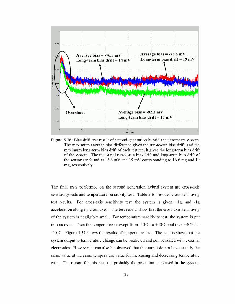
122
Average bias = -75.6 mV Long-term bias drift = 19 mV
Average bias = -76.5 mV Long-term bias drift = 14 mV
Average bias = -92.2 mV Long-term bias drift = 17 mV
Overshoot
Figure 5.36: Bias drift test result of second generation hybrid accelerometer system.
The maximum average bias difference gives the run-to-run bias drift, and the maximum long-term bias drift of each test result gives the long-term bias drift of the system. The measured run-to-run bias drift and long-term bias drift of the sensor are found as 16.6 mV and 19 mV corresponding to 16.6 mg and 19 mg, respectively.
The final tests performed on the second generation hybrid system are cross-axis
sensitivity tests and temperature sensitivity test. Table 5-6 provides cross-sensitivity
test results. For cross-axis sensitivity test, the system is given +1g, and -1g
acceleration along its cross axes. The test results show that the cross-axis sensitivity
of the system is negligibly small. For temperature sensitivity test, the system is put
into an oven. Then the temperature is swept from -40°C to +40°C and then +40°C to
-40°C. Figure 5.37 shows the results of temperature test. The results show that the
system output to temperature change can be predicted and compensated with external
electronics. However, it can also be observed that the output do not have exactly the
same value at the same temperature value for increasing and decreasing temperature
case. The reason for this result is probably the potentiometers used in the system,
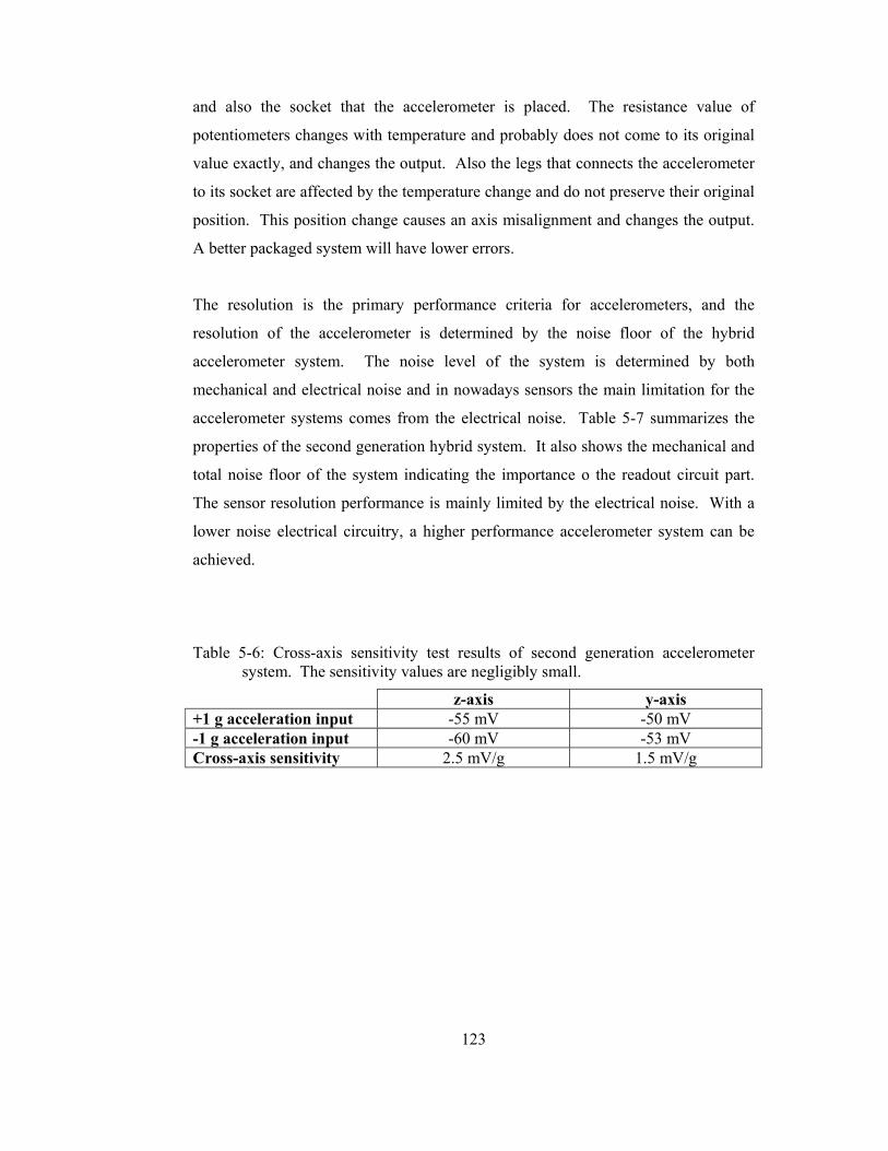
123
and also the socket that the accelerometer is placed. The resistance value of
potentiometers changes with temperature and probably does not come to its original
value exactly, and changes the output. Also the legs that connects the accelerometer
to its socket are affected by the temperature change and do not preserve their original
position. This position change causes an axis misalignment and changes the output.
A better packaged system will have lower errors.
The resolution is the primary performance criteria for accelerometers, and the
resolution of the accelerometer is determined by the noise floor of the hybrid
accelerometer system. The noise level of the system is determined by both
mechanical and electrical noise and in nowadays sensors the main limitation for the
accelerometer systems comes from the electrical noise. Table 5-7 summarizes the
properties of the second generation hybrid system. It also shows the mechanical and
total noise floor of the system indicating the importance o the readout circuit part.
The sensor resolution performance is mainly limited by the electrical noise. With a
lower noise electrical circuitry, a higher performance accelerometer system can be
achieved.
Table 5-6: Cross-axis sensitivity test results of second generation accelerometer system. The sensitivity values are negligibly small.
z-axis y-axis +1 g acceleration input -55 mV -50 mV -1 g acceleration input -60 mV -53 mV Cross-axis sensitivity 2.5 mV/g 1.5 mV/g
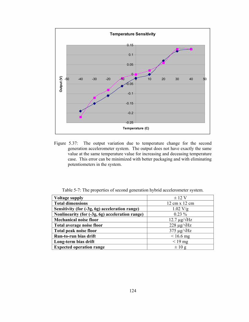
124
Temperature Sensitivity
-0.25
-0.2
-0.15
-0.1
-0.05
0
0.05
0.1
0.15
-50 -40 -30 -20 -10 0 10 20 30 40 50
Temperature (C)
Out
put (
V)
Figure 5.37: The output variation due to temperature change for the second generation accelerometer system. The output does not have exactly the same value at the same temperature value for increasing and deceasing temperature case. This error can be minimized with better packaging and with eliminating potentiometers in the system.
Table 5-7: The properties of second generation hybrid accelerometer system.
Voltage supply ± 12 V Total dimensions 12 cm x 12 cm Sensitivity (for (-3g, 6g) acceleration range) 1.02 V/g Nonlinearity (for (-3g, 6g) acceleration range) 0.23 % Mechanical noise floor 12.7 µg/√Hz Total average noise floor 228 µg/√Hz Total peak noise floor 375 µg/√Hz Run-to-run bias drift < 16.6 mg Long-term bias drift < 19 mg Expected operation range ± 10 g
125
5.4 Summary and Discussion of the Fabrication and Test Results
The designed accelerometers and gyroscopes are fabricated using three different
fabrication processes. For SOIMUMPs and nickel electroplating processes, working
accelerometer and gyroscope samples are achieved but for DRIE process, due to the
continuing optimization of the process, a working accelerometer or gyroscope
sample cannot be realized. After the fabrication, all the necessary basic tests are
done for each accelerometer and gyroscope sample, and for high performance
accelerometer samples, two hybrid accelerometer-readout circuit systems are
constructed and tested. This section gives the fabrication and tests results and
suggests future tests.
• For SOIMUMPs process, the samples are released and then diced. Due to
the shocks during the dicing operation, the gyroscope samples are
severely damaged. However, the accelerometers have thicker critical
dimensions than the gyroscopes; hence we do not encounter any damage
in the accelerometers.
• For nickel electroplating process, the samples turned out to be just as we
have expected. The formation of the mold photoresist is the critical
fabrication step in this process, and with the knowledge gained from
previous studies, we have almost perfectly characterized the shrinking of
the photoresist in the exposure step. Hence, the fabricated sensors have
almost the same resonance frequency values as we have calculated in the
design period. However, the photoresist is also deformed in the hardbake
step. This deformation cause capacitance mismatches, hence nonlinearity
in the sensor and also may cause bias drift problems.
• For the DRIE process, we have not achieved any working sensor due to
continuing optimization of the process. The wide openings are etched
away very early then the small openings and this cause notching effect in
the wide openings or unfinished etch regions in the small openings.
126
• Stiction, short circuit, sense capacitance, and resonance frequency test is
performed for every working accelerometer and gyroscope sample. The
resonance frequency tests results show that the fabricated sensors have
very similar resonance frequencies as the designed values. This fact
proves that the characterization of the process is well done in the design
period.
• First generation hybrid accelerometer system is constructed using
MS3110 commercial readout circuitry and a high performance
SOIMUMPs accelerometer. This hybrid system consists of the sensor
and the readout part only, however the bias and the amplifier circuits can
be connected externally. This hybrid system is tested in the index table
for sensitivity and nonlinearity, and also noise test is performed using a
spectrum analyzer. The system shows 22.2 mV/g sensitivity with less
than 0.1 % nonlinearity. The average noise floor and the peak noise floor
of the system are measured as 799 µg/√Hz and 1.8 mg/√Hz, respectively.
• Second generation hybrid accelerometer system is constructed using high
performance nickel electroplated accelerometer sample. This hybrid
system consists of sensor part, MS3110 readout circuit, bias circuitry, and
amplifier stages. The system is tested in the index table for nonlinearity
and sensitivity values. Moreover, the system is put into a rate table to
perform nonlinearity and sensitivity values for high acceleration values.
Noise test is performed using a spectrum analyzer, and bias drift tests are
using a computer connected multimeter. The tests show that the
accelerometer has 1.02 V/g sensitivity with less than 0.3 % nonlinearity.
The senor also has 228 µg/√Hz average noise floor and 375 µg/√Hz peak
noise floor. Run-to-run bias drift and long-term bias drift of the sensor
are found as 16.6 mg and 19 mg, respectively.
127
CHAPTER 6
CONCLUSION AND SUGGESTIONS FOR FUTURE
RESEARCH
MEMS IMUs consisting MEMS accelerometers and gyroscopes started to appear in
the market as effective and low prize solutions to inertial sensor applications.
Capacitive MEMS accelerometers and gyroscopes started to dominate MEMS
inertial sensor market with their high linearity, high sensitivity, low temperature
dependency, low noise, and low cost. This study aims to achieve low cost, high
performance accelerometer and gyroscope prototypes for some military and
commercial use IMUs, using three different fabrication techniques.
The research done during this study can be summarized as:
1. Several accelerometer topologies are investigated and the best topology
accelerometer is selected as the sensor topology. Moreover a new symmetric
and decoupled (SYMDEC) gyroscope topology is proposed. The simulations
of these topologies are done using MATLAB and COVENTORWARE.

128
2. 8 accelerometer prototypes and 4 gyroscope prototypes are designed for three
different fabrication processes. The designs are verified with MATLAB and
COVENTORWARE simulations. The mask designs for the fabrication
processes are done.
3. The nickel electroplating process fabrication and majority of DRIE process
fabrication steps are realized. SOIMUMPs process is realized CRONOS Inc.,
which is a commercial firm. Stiction, short circuit, sense capacitance, and
resonance frequency tests are performed for each accelerometer and
gyroscope sample, and high performance working accelerometer samples are
selected.
4. Using two different accelerometer prototypes, two different hybrid systems
are constructed using the accelerometer sample and MS3110 commercial
capacitive readout circuit. Sensitivity, nonlinearity, and noise test is
performed for both two prototypes. The second generation accelerometer is
also tested for bias drift values, and nonlinearity and sensitivity under high
acceleration inputs. This hybrid system satisfies the design goals with its
compact structure having bias and amplifiers included. Table 6-1 gives the
comparison of the design goals and the achieved accelerometer performance
values. Sensitivity and nonlinearity goal is provided by ASELSAN. The bias
drift goal is appropriate for some control applications in some commercial
applications. Noise floor goal enables the accelerometer to be used for some
control applications in some military and consumer applications.
5. A symmetric and decoupled gyroscope topology is realized. The resonance
frequency test of this gyroscope is done with connecting a unity gain buffer.

129
Table 6-1: Comparison of design goals and achieved accelerometer performance values.
Parameter Performance Goal Achieved Supply Voltage ± 12 V ± 12 V Sensitivity 1 V/g 1.02 V/g Noise Floor 500 µg/√Hz 375 µg/√Hz * Nonlinearity 1 % 0.23 % Bias-drift 20 mg 16.6 mg, 19 mg * * * The total peak noise floor. *We have found two kinds of bias drift as run-to-run and long-term bias drift. Each bias drift component is lower than 20 mg.
In addition to these achieved work, also some other future work can be suggested for
the development of micromachined accelerometers and gyroscopes.
1. For the nickel electroplating process development, a new mask set should be
prepared. This mask set should separate the bulky mold photoresist regions
from the critical dimensions of the sensors. This separation will prevent the
mold photoresist deformation in the hardbake step to affect the critical
structural regions of the sensors. Hence, a lower drift, with lower capacitance
mismatch sensors can be realized.
2. For the DRIE process development, a new mask set should be prepared. In
this mask set, the openings for DRIE etch regions should have very similar
widths. Hence, the etching will finish in every part of the sensor at the same
time.
3. For the accelerometer prototype construction, SMD components can be used
to occupy smaller area. Also a vacuum or inert gas packaging can be
considered. If the SMD components can also be put into the same package,
very small but well protected accelerometer system prototypes can be
realized.
130
4. A low noise open-loop or closed-loop capacitive readout circuits for
accelerometers can be designed and fabricated. As it can be seen from the
test results of the hybrid accelerometer system, the system performance is
mainly limited by the electronic noise. With a better electronic circuitry than
MS3110, higher performance accelerometer hybrid systems can be realized.
In conclusion, the most important contribution of this work is construction of an
accelerometer system that is composed of a MEMS accelerometer, a readout circuit,
bias circuitries for this readout circuit, and external amplifier electronics. This
system is the highest performance accelerometer system developed in Turkey. In
addition, asymmetric and decoupled gyroscope topology is proposed and its
operation is verified. The fabrication processes that are currently used in METU
facilities are also improved with the gained knowledge and experience. It is hoped
that this work will be an important step in developing tactical and inertial grade
IMUs in METU.
131
REFERENCES
[1] M. D. Pottenger, “Design of Micromachined Inertial Sensors,” PhD. Dissertation, Univ. of California, 2001.
[2] J. E. D. Williams, “From Sails to Satellites: The Origin and Development of
Navigational Science,” New York, Oxford University Press, 1994. [3] S. E. Alper, “Silicon Surface Micromachined Gyroscopes Using MEMS
Technology,” M.S. Thesis, Middle East Technical Univ., 2000. [4] K. Kumar, N. Barbour, and J. M. Elwell, “Emerging Low(er) Cost Inertial
Sensors,” Proc. AIAA GN&C Conf., pp. 11-24, August 1992. [5] M. Kraft, “Micromachined Inertial Sensors: The State of the Art and a Look
into Future,” IMC Measurement and Control, Vol. 33 No. 6, pp. 164-168, 2000.
[6] N. Yazdi, F. Ayazi, and K. Najafi, “Micromachined Inertial Sensors,” Proc.
of the IEEE, Vol. 86, No 8, pp. 1640-1659, August 1998. [7] H. Kulah, “Closed-Loop Electromechanical Sigma-Delta Microgravity
Accelerometers,” PhD. Dissertation, Univ. of Michigan, 2003. [8] J. Dosher and C. Kitchin, “Monitoring Machine Vibration with
Micromachined Accelerometers,” Sensors 14(5), pp. 33-34, May 1997. [9] P. F. Man, and C. H. Mastrangelo, “Surface micromachined shock sensor for
impact detection,” Tech. Digest of IEEE Solid-State Sensors and Actuator Workshop (Hilton Head’94), pp.156-159, 1994.
[10] R. S. Seeley, “Micromachines Rev Up for Fast Growth,” Electronic Business
Today, pp- 33-38, April 1996. [11] R. F. Yazıcıoğlu, “Surface Micromachined Capacitive Accelerometers Using
MEMS Technology,” M.S. Thesis, Middle East Technical Univ. ,2003.

132
[12] N. Barbour, G. Schmidt, “Inertial Sensor Technology Trends,” Workshop on Autonomous Underwater Vehicles, pp.55-62, 1998.
[13] R. L. Craik and C. A. Oatis (Eds.), “Gait Analysis: Theory and Applications,”
Mosby, 1995. [14] K. Miller, D. Hendelman, C. Baggett, E. Debold, and P. Freedson,
“Validation of Accelerometry to Assess Moderate Intensity Physical Activity in the Field,” Medicine & Science in Sports & Exercise, 31(5), pp.43, May 1999.
[15] W. Kuehnel and S. Sherman, “A surface micromachined silicon
accelerometer with on-chip detection circuitry,” Sensors and Actuators Vol. A-45, pp. 7-16, 1994.
[16] S. J. Sherman, W. K. Tsang, T. A. Core, R. S. Payne, D. E. Quinn, K. H. L.
Chau, J. A. Farash, and S. K. Baum, “A Low Cost Monolithic Accelerometer: Product/Technology Update,” Techncal Digest International Electron Devices Meeting, pp.501-504, 1992.
[17] K. Jost, “Yaw Sensing,” Automotive Engineering, pp. 61-63, September 1995. [18] G. He and K. Najafi, “A Single-Crystal Silicon Vibrating Ring Gyroscope,”
Proc. IEEE Micro Electro Mechanical Systems Workshop (MEMS’02), pp. 718-721, January 2002.
[19] W. Qu, C. Wenzel, and G Gerlach, “Fabrication of a 3D Differential-
Capacitive Accelerometer by UV-LIGA,” Sensors and Actuators, Vol. 77, pp. 14-20, 1999.
[20] J. W. Wiegold, K. Najafi, ans S. W. Pang, “Design and Fabrication of
Submicrometer, Single Crystal Si Accelerometer,” Journal of Microelectromechanical Systems, Vol.10, pp. 558-524, Dec.2001.
[21] K. H. –L. Chau, S. R. Lewis, Y. Zhao, R.T. Howe, S. F. Bart, and R. G.
Marcheselli, “An Integrated Force-Balanced Capacitive Accelerometer for low-g Applications,” Sensors and Actuators, Vol. 54, pp. 472-476, 1996.
[22] B. Guldimann, P. Thiebauld, N. F. de Rooji, and R. A. Turpin,
“Micromachined, Fiber-Optic Based Accelerometer with Shutter Modulation,” Proc. IEEE Micro Electro Mechanical System Workshop (MEMS’00), 2000.
[23] A. Partidge, J. K. Reynolds, B. W. Chui, E. M. Chow, A. M. Fitzgerald, L.
Zhang, and N.I. Maluf, “A High-Performance Planar Piozoresistive Accelerometer,” J. Microelectromechanical Sys., Vol. 9, No. 1, pp. 58-66, March 2000.
133
[24] H. Takao, Y. Matsumoto, and M. Ishida, “Stress-sensitive Differential Amplifiers Using Piozoresistive Effects of MOSFETs and Their Application to Three-Axis Accelerometers,” Sensors and Actuators, Vol. 65, pp. 61-68, 1998.
[25] J. A. Plaza, M. A. Benitz, and Lora-Tamayo, “New FET Accelerometer
Based on Surface Micromachining,” Sensors and Actuators, Vol. 61, pp. 342-345, 1997.
[26] S. D. Senturia, “Microsystem Design,” Kluwer Academic Publishers, 2001. [27] F. Paelotti, “A Silicon Micromachined Vibrating Gyroscope with
Piezoresistive Detection and Electromagnetic Excitation,” MEMS’96, pp.162-167, 1996.
[28] R. Voss, “Silicon Angular Rate Sensor for Automotive Applications with
Piezoelectric Drive and Piezoresistive Read-out,” Transducers’97, Vol.2 pp.879-882, 1997.
[29] Y. Nemirovsky, A. Nemirovsky, P. Muralt, and N. Setter, “Design of Novel
Thin-Film Piezoelectric Accelerometer,” Sensors and Actuators, Vol. 56, pp. 239-249, 1996.
[30] D. L. DeVoe, and A. P. Pisano, “Surface Micromachined Piezoelectric
Accelerometers (PiXLs),” J. Microelectromechanical Sys., Vol. 10, No. 2, pp. 180-186, June 2001.
[31] http://www.murata.com/ninfo/nr0283e.html [32] V. Milanovi, E. Bowen, N. Tea, J. Suehle, B. Payne, M. Zaghloul, and M.
Gaitan, “Convection-Based Accelerometer and Tilt Sensor Implemented in Standard CMOS,” Proc. Int. Mech. Eng. Conf. and Exp., MEMS Symposium, Anaheim, Nov. 1998.
[33] A. A. Seshia, M. Palaniapan, T. A. Roessing, R. T. Howe, R. W. Gooch, T. R.
Schimert, and S. Montague, “A Vacuum Packaged Surface Micromachined Resonant Accelerometer,” J. Microelectromechanical Sys., Vol. 11, No. 6, pp. 784-793, Dec 2002.
[34] C.–H. Lui and T. H. Kenny, “A High-Precision, Wide-Bandwidth
Micromachined Tunneling Accelerometer,” J. Microelectromechanical Sys., Vol. 10, No. 3, pp. 425-433, Sept. 2001.
[35] F. Gretillat, M.-A. Gretillat, and N. F. de Rooij, “Improved Design of a
silicon Micromachined Gyroscope with Piezoresistive Detection and Electromagnetic Actuation,” J. Microelectromechanical Sys., Vol. 8, No. 3, pp. 243-250, September 1999.
134
[36] A. J. Harris, J. S. Burdess, D. Wood, R. Langford, G. Williams, M. C. L. Lard, and M. E. McNie, “Issues Associated with the Design, Fabrication and Testing of a Crystalline Silicon Ring Gyroscope with Electromagnetic Actuation and Sensing,” J. Micromech. Microeng., pp. 284-292, August 1998.
[37] F. P. Beer and E. R. Johnston, “Mechanics of Materials,” McGraw-Hill, 1985. [38] R. J. Roark and W. C. Young, “Formulas for Stress and Strain,” McGraw-
Hill, 1983. [39] M. W. Putty, “A Micromachined Vibrating Ring Gyroscope,” PhD.
Dissertation, Univ. of Michigan, 1995. [40] A. Burstein, “Highly Sensitive Single and Dual-Axis High Aspect Ratio
Accelerometers with a CMOS Precision Interface Circuit,” PhD Dissertation, Univ. of California, 1999.
[41] W. T. Thomson and M. D. Dahleh, “Theory of Vibration with Applications,”
Prentice Hall, 1998. [42] T. Veijola, H. Kuisma, and J. Lahdenpera, “The Influence of Gas-Surface
Interaction on Gas-Film Damping in a Silicon Accelerometer,” Sensors and Actuators, Vol. 66, pp. 83-92, 1998.
[43] T. Veijola, H. Kuisma, J. Lahdenpera, and T. Rayhanen, “Equivalent-Circuit
Model of the Squeezed Gas Film in a Silicon Accelerometer,” Sensors and Actuators, Vol. A-48, pp. 239-248, 1995.
[44] M. A. Lemkin, “Micro Accelerometer Design with Digital Feedback
Control,” PhD. Dissertation, Univ. of California, Berkeley, 1997. [45] Y. J. Yang and C. J. Yu, “Macromodel Extraction of Gas Damping Effects
for Perforated Surfaces with Arbitrary Shaped Geometries,” Modeling and Simulation of Microsystems, pp. 178-181, 2002.
[46] P. C. Yen and Y. J. Yang, “Time-Domain Reduced-Order Models for Lateral
Viscous Damping Effects for 3-D Geometries,” Modeling and Simulation of Microsystems, pp. 190-193, 2002.
[47] A. Duwel, M. Weinstein, J. Gorman, J. Borenstein, and P. Ward, “Quality
Factors of MEMS Gyros and the Role of Thermoelastic Damping,” Proc. IEEE Micro Electro Mechanical Systems Workshop (MEMS’02), pp. 214-219, January 2002.
[48] J. Chae, H. Kulah, and K. Najafi, “An All-Silicon In-Plane High-Sensitivity
Low-Noise Micro-G Micromachined Accelerometer,” Proc. IEEE Micro Electro Mechanical Systems Workshop (MEMS’03), pp. 466-469, January 2003.
135
[49] W. Geiger, W. U. Butt, A. Gaiβer, J. Frech, M. Braxmaier, T. Link, A. Kohne, P. Nommensen, H. Sandmaier, and W. Lang, “Decoupled Microgyros and The Design Principle DAVED,” Tech. Dig. IEEE Micro Electro Mechanical Systems Conf. (MEMS 2001), pp. 170-173, January 2001.
[50] W. A. Clark and R. T. Howe, “Surface Micromachined Z-Axis Vibratory
Rate Gyroscope,” Tech. Dig. Solid-State Sensor and Actuator Workshop, , pp. 283-287, June 1996.
[51] X. Jiang, J. I. Seeger, M. Kraft, and B. E. Boser, “A Monolithic Surface
Micromachined Z-Axis Gyroscope with Digital Output,” Symp. on VLSI Circuits Dig. of Tech. Papers, , pp. 16-19, June 2000.
[52] B. E. Boser, “Capacitive Sensor Interfaces,” Univ. of Berkeley, pp. 1-41,
1996. [53] J. R. Vig and Y. Kim, “Noise in Microelectromechanical System
Resonators,” IEEE Trans. On Ultrasonics, Ferroelectrics, and Frequency Control, Vol. 46, No.6, pp. 1558-1565, Nov. 1999.
[54] IEEE Standard Specification Format Guide and Test Procedure for
Linear, Single-Axis, Pendulous, Analog Torque Balance Accelerometers, 1972.
[55] G. K. Fedder, “Simulation of Microelectromechanical Systems,” Ph.D.
Dissertation, Univ. of California, Berkeley, 1994. [56] F. Ayazi, H. H. Chen, F. Kocer, G. He, and K. Najafi, “A High Aspect Ratio
Polysilicon Vibrating Ring Gyroscope,” Digest, Solid-State Sensors and Actuators Workshop, pp 289-292, June 2000.
[57] S. An, Y. S. Oh, B. L. Lee, K. Y. Park, S. J. Kang, S. O. Choi, Y. I. Go, and
C. M. Song, “Dual-Axis Microgyroscope with Closed-Loop Detection,” Proc. IEEE Micro Electro Mechanical Systems Workshop (MEMS’98), pp. 328-333, 1998.
[58] www.memscap.com/memsrus/docs/SOIMUMPs.DR.4.0.pdf [59] J. Chae, H. Kulah, H. Najafi, “A Hybrid Silicon-On-Glass (SOG) Lateral
Micro-Accelerometer With CMOS Readout Circuitry,” Proc. IEEE Micro Electro Mechanical Systems Workshop (MEMS’02), pp. 623-626, Jan 2002.
[60] P. J. French and P. M. Sarro, “Surface versus Bulk Micromachining: The
Contest for Suitable Applications,” J. Micromech. Microeng., pp. 45-53, August 1998.
[61] M. J. Madou, “Fundementals of Microfabrication: The science of
Miniaturization,” CRC, 2002.
136
[62] G. T. Kovacs, N. I. Maluf, and K. E. Petersen, “Bulk Micromachining of Silicon,” Proc. IEEE, Vol. 86, No. 8, pp. 1536-1551, August 1998.
[63] J.-L. Yeh, “Integrated Polysilicon Surface and DRIE Bulk Silicon
Micromachined Devices,” Ph.D. dissertation, Cornell University, 2000. [64] B. Loechel, "Thick-layer Resists for Surface Micromachining," J. Micromech.
Microeng. Vol. 10, No. 2, pp. 108-115, June 2000. [65] H. Kuisman, T. Ryhanen, J. Lahpendera, E. Punkka, S. Routsalainen, T.
Sillanpaa, and H. Sepa, “A Bulk Micromachined Silicon Angular Rate Sensor,” Tech. Dig. 9th Int. Conf. Solid-State Sensors and Actuators (Transducers’97), pp. 875-878, June 1997.
[66] T. K. Tang, R. C. Gutierrez, J. Z. Wilcox, C. Stell, V. Vorperian, R. Calvet,
W. J. Li, I. Charkaborty, R. Bartman, and W. J. Kaiser, “Silicon Bulk Micromachined Vibratory Gyroscope,” Tech. Dig. Solid-State Sensors and Actuators Workshop, pp. 288-293, June 1996.
[67] G. I. Andersson, N. Hedenstierna, P. Svensson and Hakan Pettersson, “A
Novel Silicon Bulk Gyroscope,” Tech. Dig. 10th Int. Conf. Solid-State Sensors and Actuators (Transducers’99), pp. 902-905, June 1999.
[68] R.P. van Kampen and R. F. Wolffenbuttel, “Modeling the Mechanical
Behaviour of Bulk-Micromachined Silicon Accelerometers,” Sensors and Actuators, Vol. 64, pp. 137-150, 1998.
[69] Y. Oh, B. Lee, S. Baek, H. Kim, J. Kim, S. Kang, and C. Song, “A Surface-
Micromachined Tunable Vibratory Gyroscope,” Proc. IEEE Micro Electro Mechanical Sytems Workshop (MEMS’97), pp. 272-277, 1997.
[70] W. A. Clark and R. T. Howe, “Surface Micromachined Z-axis Vibratory Rate
Gyroscope,” Tech. Dig. Solid-State Sensor and Actuator Workshop, pp. 283-287, June 1996.
[71] K. Funk, H. Emmerich, A. Schilp, M. Offenberg, R. Neul, and F. Larmer, “A
Surface Micromachined Silicon Gyroscope Using a Thick Polysilicon Layer,” Proc. IEEE Micro Electro Mechanical Systems Workshop (MEMS’99), pp. 57-60, January 1999.
[72] C. Hierold, A. Hildebrandt, U. Naher, T. Scheiter, B. Mensching, M. Steger,
and R. Tielert, “A Pure CMOS Surface-Micromachined Integrated Acelerometer,” Sensors and Actuators, Vol. 57, pp. 111-116, 1996.
[73] B. E. Boser and R. T. Howe, "Surface Micromachined Accelerometers,"
IEEE J. Solid-State Cct, Vol. 31, No.3, pp. 366-375, March 1996.
137
[74] N. Yazdi and K. Najafi, “An All-Silicon Single-Wafer Micro-g Accelerometer with a Combined Surface and Bulk Micromachining Process,” J. Microelectromechanical Sys., Vol. 9, No. 4, pp. 544-550, December 2000.
[75] S. Lee, S. Park, J. Kim, S. Lee, and Dong-il (Dan) Cho, “Surface/Bulk
Micromachined Single-Crystalline-Silicon Micro-Gyroscope,” J. Microelectromechanical Sys., Vol. 9, No. 4, pp. 557-567, December 2000.
[76] C. Lu, M. Lemkin, and B. E. Boser, “A Monolithic Surface Micromachined
Accelerometer with Digital Output,” IEEE Journal of Solid-State Circuits, Vol. 30, No. 12, pp. 1367-1373, Dec. 1995.
[77] J. Gobet, F. Cardot, J. Bergqvist, and F. Rudolf, “Electrodeposition of 3D
Microstructures on Silicon,” J. Micrimech. Microeng. Vol. 3, No. 3, pp. 123-130, September 1993.
[78] W. Ruythooren, K. Attenborough, S. Beerteen, P. Merken, J. Fransaer, E.
Beyne, C. Van Hoof, J. De Boeck, and J. P. Celic, “Electrodeposition for the Synthesis of Microsystems,” J. Micromech. Microeng. Vol. 10, No. 2, pp. 101-107, June 2000.
[79] Shipley Microposit SJR 5000 Photoreisit Datasheet. [80] X. Li, S. Kiyawat, H. J. Santos, and C. J. Kim, “High-Aspect-Ratio
Electroplated Structures with 2 µm Beamwidth,” Proc. MEMS (MEMS-Vol.1), ASME Int. Mechanical Eng. Congress and Exposition, pp. 25-30, Nov. 1999.
[81] F. Laermer, A. Schilp, K. Funk, and M. Offenberg, “Bosch Deep Silicon
Etching: Improving Uniformity and Etch Rate for Advanced MEMS Applications,” Proc. IEEE Micro Electro Mechanical Systems Workshop (MEMS’99), pp. 211-216, January 1999.
[82] M. Chabloz, J. Jiao, Y. Yoshida, T. Matsuura, and K. Tsutsumi, “A Method
to Evade Microloading Effect in Deep Reactive Ion Etching for Anodically Bonded Glass-Silicon Structures,” Proc. IEEE Micro Electro Mechanical Systems Workshop (MEMS 2000), pp. 283-287, January 2000.
[83] M. A. Schimidt, “Wafer-to-wafer bonding for microstructure formation,”
Proc. IEEE, Vol. 86, pp. 1574-1585, Aug 1998. [84] G. Willis, “Direct-current polarization during field-assisted glass-metal
sealing,” J. Amer. Ceramic. Soc. Vol. 53, pp. 563-567, 1970. [85] T. M. H. Lee, I.-M. Hsing, and C. Y. N. Liaw, “An Improved Anodic
Bonding Process Using Pulsed Voltage Technique,” J. Microelectromechanical Sys., Vol. 9, No. 4, pp. 469-473, December 2000.


![Design of ‘Smart’ pebble for sediment entrainment studyal [1]). ADXL202 dual axis accelerometers and ADXRS150 yaw rate gyroscopes were found suitable. These devices were placed](https://static.fdocuments.in/doc/165x107/5f173d0cbe131b05f424c7c4/design-of-asmarta-pebble-for-sediment-entrainment-study-al-1-adxl202-dual.jpg)