Memory Storage Product Selection Guide
28
Memory and Storage April 2005 Product Selection Guide
Transcript of Memory Storage Product Selection Guide

Memory and StorageApril 2005
Product Selection Guide

2a
MEMORY AND STORAGE
DRAM
DDR2 SDRAM
DDR SDRAM
SDRAM
RDRAM
NETWORK DRAM
MOBILE SDRAM
GRAPHICS DDR SDRAM
DRAM ORDERING INFORMATION
FLASH
NAND, OneNAND, NOR FLASH
NAND FLASH ORDERING INFORMATION
SRAM
LOW-POWER SRAM
LOW-VOLTAGE AND LOW-POWER SRAM
MICRO-POWER AND LOW-VOLTAGE SRAM
HIGH DENSITY, LOW POWER (UtRAM)
HIGH-SPEED ASYNCHRONOUS FAST SRAM
SPB & FT SRAM
SPB & FT NTRAM
LATE-WRITE R-R SRAM
DDR1 SRAM
QDR1 SRAM
DDR2 SRAM
QDR2 SRAM
SRAM ORDERING INFORMATION
MULTI-CHIP PACKAGE
NAND/DRAM
NOR/SRAM and NOR/UtRAM
OneNAND/DRAM
NOR/DRAM
NOR/OneNAND/UtRAM
STORAGE
OPTICAL MEDIA SOLUTIONS
HARD DISK DRIVES
SECTION A PAGE
3a
4a-5a
5a-7a
7a
7a
8a
8a
9a-11a
12a
13a
14a
14a
14a
15a
15a
15a-16a
16a-17a
17a
17a-18a
18a
19a
19a
20a-21a
22a
23a
23a
23a
24a
25a
26a
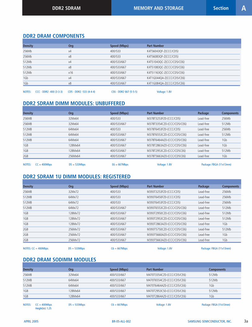
DDR2 DRAM COMPONENTS
Density Org Speed (Mbps) Part Number
256Mb x4 400/533 K4T56043QF-Z(CCC/CD5)
256Mb x8 400/533 K4T56083QF-Z(CCC/CD5)
512Mb x4 400/533/667 K4T51043QC-Z(CCC/CD5/CE6)
512Mb x8 400/533/667 K4T51083QC-Z(CCC/CD5/CE6)
512Mb x16 400/533/667 K4T51163QC-Z(CCC/CD5/CE6)
1Gb x4 400/533/667 K4T1G044QA-Z(CCC/CD5/CE6)
1Gb x8 400/533/667 K4T1G084QA-Z(CCC/CD5/CE6)
NOTES: CCC - DDR2 -400 (3-3-3) CD5 - DDR2 -533 (4-4-4) CE6 - DDR2 667 (5-5-5) Voltage: 1.8V
DDR2 SDRAM DIMM MODULES: UNBUFFERED
Density Org Speed (Mbps) Part Number Package Components
256MB 32Mx64 400/533 M378T3253FZ0-(CCC/CD5) Lead-free 256Mb
256MB 32Mx64 400/533/667 M378T3354CZ0-(CCC/CD5/CE6) Lead-free 512Mb
512MB 64Mx64 400/533 M378T6453FZ0-(CCC/CD5) Lead-free 256Mb
512MB 64Mx64 400/533/667 M378T6553CZ0-(CCC/CD5/CE6) Lead-free 512Mb
512MB 64Mx64 400/533/667 M378T6464AZ0-(CCC/CD5/CE6) Lead-free 1Gb
1GB 128Mx64 400/533/667 M378T2863AZ0-(CCC/CD5/CE6) Lead-free 1Gb
1GB 128Mx64 400/533/667 M378T2953CZ0-(CCC/CD5CE6) Lead-free 512Mb
2GB 256Mx64 400/533/667 M378T5663AZ0-(CCC/CD5CE6) Lead-free 1Gb
NOTES: CC = 400Mbps D5 = 533Mbps E6 = 667Mbps Voltage: 1.8V Package: FBGA (11x13mm)
DDR2 SDRAM 1U DIMM MODULES: REGISTERED
Density Org Speed (Mbps) Part Number Package Components
256MB 32Mx72 400/533 M393T3253FZ0-(CCC/CD5) Lead-free 256Mb
512MB 64Mx72 400/533 M393T6450FZ0-(CCC/CD5) Lead-free 256Mb
512MB 64Mx72 400/533 M393T6453FZ0-(CCC/CD5) Lead-free 256Mb
512MB 64Mx72 400/533/667 M393T6553CZ0-(CCC/CD5/CE6) Lead-free 512Mb
1GB 128Mx72 400/533/667 M393T2950CZ0-(CCC/CD5/CE6) Lead-free 512Mb
1GB 128Mx72 400/533/667 M393T2953CZ0-(CCC/CD5/CE6) Lead-free 512Mb
1GB 128Mx72 400/533/667 M393T2863AZ0-(CCC/CD5/CE6) Lead-free 1Gb
2GB 256Mx72 400/533/667 M393T5750CZ0-(CCC/CD5/CE6) Lead-free 512Mb
2GB 256Mx72 400/533/667 M393T5660AZ0-(CCC/CD5/CE6) Lead-free 1Gb
2GB 256Mx72 400/533/667 M393T5663AZ0-(CCC/CD5/CE6) Lead-free 1Gb
NOTES: CC = 400Mbps D5 = 533Mbps C6 = 667Mbps Voltage: 1.8V Package: FBGA (11x13mm)
DDR2 DRAM SODIMM MODULES
Density Org Speed (Mbps) Part Number Components
256MB 32Mx64 400/533/667 M470T3354CZ0-(CCC/CD5/CE6) 512Mb
512MB 64Mx64 400/533/667 M470T6554CZ0-(CCC/CD5/CE6) 512Mb
512MB 64Mx64 400/533/667 M470T6464AZ0-(CCC/CD5/CE6) 1Gb
1GB 128Mx64 400/533/667 M470T2953CS0-(CCC/CD5/CE6) 512Mb
1GB 128Mx64 400/533/667 M470T2864AZ0-(CCC/CD5/CE6) 1Gb
NOTES: CC = 400Mbps D5 = 533Mbps C6 = 667Mbps Voltage: 1.8V Package: FBGA (11x13mm) Height(in): 1.25
ASection MEMORY AND STORAGE
3a
DDR2 SDRAM
SAMSUNG SEMICONDUCTOR, INC.APRIL 2005 BR-05-ALL-002

ASection MEMORY AND STORAGE
4a
DDR SDRAM
SAMSUNG SEMICONDUCTOR, INC. APRIL 2005BR-05-ALL-002
DDR SDRAM COMPONENTS
Density Org Speed (Mbps) Part Number Package Notes256M 64Mx4 266/333/400 K4H560438E-TC(L)B0/B3/CCC 66 pin TSOP Pb-free available
256M 64Mx4 333/400 K4H560438E-GC(L)B3/CCC 60 ball FBGA Pb-free available
256M 32Mx8 266/333/400 K4H560838E-TC(L)B0/B3/CCC 66 pin TSOP Pb-free available
256M 32Mx8 333/400 K4H560838E-GC(L)B3/CCC 60 ball FBGA Pb-free available
256M 16Mx16 266/333/400 K4H561638F-TC(L)B0/B3/CCC 66 pin TSOP Pb-free available
256M 16Mx16 333/400 K4H561638F-GC(L)B3/CCC 60 ball FBGA Pb-free available
512M 128Mx4 266/333/400 K4H510438C-UC(L)B0/B3/CCC 66 pin TSOP Pb-free available
512M 128Mx4 266/333/400 K4H510438C-ZC(L)B0/B3/CCC 60 ball FBGA Pb-free
512M 64Mx8 266/333/400 K4H510838C-UC(L)B0/B3/CCC 66 pin TSOP Pb-free
512M 64Mx8 266/333/400 K4H510838C-VC(L)B0/B3/CCC 54 pin Shrink TSOP Pb-free
512M 64Mx8 266/333/400 K4H510838C-ZC(L)B0/B3/CCC 60 ball FBGA Pb-free
512M 32Mx16 333/400 K4H511638C-UC(L)B3/CCC 66 pin TSOP Pb-free
512M 32Mx16 333/400 K4H511638C-ZC(L)B3/CCC 60 ball FBGA Pb-free
1Gb 256Mx4 266/333 K4H1G0438M-TC(L)B0/B3 66 pin TSOP
1Gb 128Mx8 266/333 K4H1G0838M-TC(L)B0/B3 66 pin TSOP
NOTES: B0 = DDR266 (133MHz @ CL=2.5) A2 = DDR266 (133MHz @ Cl=2) B3 = DDR333 (166MHz @ CL=2.5) CC = DDR400 (200MHz @ CL=3)
DDR SDRAM DIMM MODULES: UNBUFFERED
Density Org Speed (Mbps) Composition Part Number Notes
256MB 32Mx64 266/333 (32M x 8)*8 M368L3223ETN - CB0/B3 Pb-free available
256MB 32Mx64 400 (32M x 8)*8 M368L3223ETM - CCC00 Pb-free available
256MB 32Mx64 333/400 (32M x 8)*8 M368L3223FTN- CB3/CCC Pb-free available
256MB 32Mx72 266/333/400 (32M x 8)*9 M381L3223ETM - CB0/B3/CCC Pb-free available
256MB 32Mx72 333/400 (32M x 8)*9 M381L3223FTM- CB3/CCC Pb-free available
512MB 64Mx64 266/333 (32M x 8)*16 M368L6423ETN- CB0/B3 Pb-free available
512MB 64Mx64 400 (32M x 8)*16 M368L6423ETM - CCC00 Pb-free available
512MB 64Mx64 333/400 (32M x 8)*16 M368L6423FTN- CB3/CCC Pb-free available
512MB 64Mx72 266/333/400 (32M x 8)*18 M381L6423ETM - CB0/B3/CCC Pb-free available
512MB 64Mx72 333/400 (32M x 8)*18 M381L6423FTM- CB3/CCC Pb-free available
512MB 64MX64 266/333/400 (64M x8) *8 M368L6523CUS- CB0/B3/CCC Pb-free
512MB 64Mx72 266/333/400 (64M x 8)*9 M381L6523CUM - CB0/B3/CCC Pb-free
1GB 128Mx64 266/333/400 (64M x 8)*16 M368L2923CUN- CB0/B3/CCC Pb-free
1GB 128Mx72 266/333/400 (64M x 8)*18 M381L2923CUM - CB0/B3/CCC Pb-free
2GB 256Mx64 266/333 (128M x 8)*16 M368L5623MTN - CB0/B3
2GB 256Mx72 266/333 (128M x 8)*18 M381L5623MTM - CB0/B3
NOTES: B0 = DDR266 (133MHz @ CL=2.5) A2 = DDR266 (133MHz @ Cl=2) B3 = DDR333 (166MHz @ CL=2.5) CC = DDR400 (200MHz @ CL=3) Type: 184-pin Package: TSOP components Voltage: 2.5V

5a
ASection MEMORY AND STORAGEDDR SDRAM
SAMSUNG SEMICONDUCTOR, INC.APRIL 2005 BR-05-ALL-002
DDR SDRAM 1U DIMM MODULES: REGISTEREDComponent # Banks
Density Org Speed (Mbps) Composition Part Number Package Module Notes
256MB 32Mx72 266 (32Mx8)*9 M312L3223ETS -C(L)B0 TSOP 1
256MB 32Mx72 333/400 (32Mx8)*9 M312L3223EG0 - C(L)/B3/CCC FBGA 1
512MB 64Mx72 266 (32Mx8)*18 M312L6423ETS - C(L)B0 TSOP 2
512MB 64Mx72 333/400 (32Mx8)*18 M312L6423EG0 - C(L)B3/CCC FBGA 2
512MB 64Mx72 333/400 (64Mx4)*18 M312L6420EG0- C(L)B3/CCC FBGA 2
512MB 64Mx72 266 (64Mx8)*9 M312L6523CUS - CB0 TSOP 1 Pb-free
512MB 64Mx72 333/400 (64Mx8)*9 M312L6523CZ0 - B3/CCC FBGA 1 Pb-free
1GB 128Mx72 333/400 (128Mx4)*18 M312L2920CZ0 - B3/CCC FBGA 1 Pb-free
2GB 256Mx72 266 (St. 256Mx4)*18 M312L5628CU0 - CB0 TSOP 2 Pb-free
2GB 256Mx72 333/400 (128Mx4)*36 M312L5720CZ0 - B3/CCC FBGA 2 Pb-free
4GB 512Mx72 266/333 (St. 512Mx4)*18 M312L5128MT0 - CB0/B3 TSOP 2
NOTES: B0 = DDR266 (133MHz @ CL=2.5) A2 = DDR266 (133MHz @ Cl=2) B3 = DDR333 (166MHz @ CL=2.5) CC = DDR400 (200MHz @ CL=3)Type: 184-pin
DDR DRAM SODIMM MODULESComponent # Banks
Density Org Speed (Mbps) Composition Part Number Package Module Notes
128MB 16Mx64 333 (16M x 16)*4 M470L1624FT0 - C(L)B3 TSOP 1
256MB 32Mx6 333 (16M x 16)*8 M470L3224FT0 - C(L)B3 TSOP 2
512MB 32Mx64 333 (32M x 16)*4 M470L3224CU0 - C(L)B3 TSOP 1 Pb-free
1GB 64Mx64 333 (64M x 8)*16 M470L2923BN0 - C(L)B3 Shrink TSOP 2
NOTES: B0 = DDR266 (133MHz @ CL=2.5) A2 = DDR266 (133MHz @ Cl=2) B3 = DDR333 (166MHz @ CL=2.5) CC = DDR400 (200MHz @ CL=3)Type: 200-pin, Double Sided Height(in): 1.25
SDRAM COMPONENTSPkg
Density Org Speed (Mbps) Part Number Refresh TSOP Comments
16Mb 1Mx16 125/143/166/183 K4S161622H-TC(L)(80/70/60/55) 2K 50 2 Banks
64Mb 16Mx4 133/143 K4S640432H-TC(L)(75/70)000 4K 54
64Mb 8Mx8 133/143 K4S640832H-TC(L)(75/70)000 4K 54
64Mb 4Mx16 133/143/166 K4S641632H-TC(L)(75/70/60)000 4K 54
64Mb 2Mx32 143/166/183/209 K4S643232H-TC(L)(70/60/55/50)000 4K 86
128Mb 32Mx4 133 K4S280432F-TC(L)(75)000 4K 54
128Mb 16Mx8 133 K4S280832F-TC(L)(75)000 4K 54
128Mb 8Mx16 133/166 K4S281632F-TC(L)(75/60)000 4K 54
256Mb 64Mx4 133 K4S560432E-TC(L)(75)000 8K 54
256Mb 32Mx8 133 K4S560832E-TC(L)(75)000 8K 54
256Mb 16Mx16 133/166 K4S561632E-TC(L)(75/60)000 8K 54
512Mb 128Mx4 133 K4S510632C-TC(L)(75)000 8K 54 stacked
512Mb 64Mx8 133 K4S510732C-TC(L)(75)000 8K 54 stacked
512Mb 128Mx4 133 K4S510432B-TC(L)(75)000 8K 54
512Mb 64Mx8 133 K4S510832B-TC(L)(75)000 8K 54
512Mb 32Mx16 133 K4S511632B-TC(L)(75)000 8K 54
1Gb 256Mx4 133 K4S1G0632B-TC(L)(75)000 8K 54 stacked
NOTES: The “1H” in the part number signifies an Intel PC100 SDRAM spec compliant device at CAS latency of 2.
The “1L” in the part number signifies an Intel 100MHz SDRAM spec compliant device at CAS latency of 3.
The “7C” in the part number signifies an Intel 133MHz SDRAM spec compliant device at CAS latency of 2L = Commercial Temp., Low Power# Banks: 4Package: TSOPVoltage: 3.3VSpeed: PC133 (133MHz CL=3/PC100 CL2)

ASection MEMORY AND STORAGE
6a
SDRAM
SAMSUNG SEMICONDUCTOR, INC. APRIL 2005BR-05-ALL-002
SDRAM DIMM MODULES PC133 COMPLIANT: REGISTEREDDensity Org Speed (Mbps) Composition Part Number # Banks Refresh Comments
Module
128MB 16Mx72 PC133 (16Mx8)*9 M390S1723FT1-C7A00 1 4K
256MB 32Mx72 PC133 (32Mx4)*18 M390S3320FT1-C7A00 2 4K
256MB 32Mx72 PC133 (32Mx8)*9 M390S3253ET1-C7A00 1 4K
512MB 64Mx72 PC133 (64Mx4)*18 M390S6450ET1-C7A00 2 8K
512MB 64Mx72 PC133 (32Mx8)*18 M390S6453BT1-C7A00 2 8K
1GB 128Mx72 PC133 (St.128Mx4)*18 M390S2858ET1-C7A00 2 8K stacked
1GB 128Mx72 PC133 (128Mx4)*18 M390S2950BT1-C7A00 2 8K
2GB 256Mx72 PC133 (St.256Mx4)*18 M390S5658BT1-C7A00 2 8K stacked; avail Q204
NOTES: Type: 168-pin, double sided Package: TSOP components Voltage: 3.3V
1U SDRAM DIMM MODULES PC133 / PC100 COMPLIANT: REGISTEREDLOW-PROFILE DIMMs (1.2 IN HEIGHT)
# Banks
Density Org Speed Composition Part Number Module Refresh Comments
128MB 16Mx72 PC133 (16x8)*9 M390S1723FTU - C7A00 1 4K
256MB 32Mx72 PC133 (32Mx4)*18 M390S3320FTU - C7A00 2 4K
256MB 32Mx72 PC133 (32Mx8)*9 M390S3253ETU - C7A00 1 8K
512MB 64Mx72 PC133 (64Mx4)*18 M390S6450ETU - C7A00 2 8K
1GB 128Mx72 PC133 (St.128Mx4)*18 M390S2858ETU - C7A00 2 8K stacked
1GB 128Mx72 PC133 (128Mx4)*18 M390S2950BTU - C7A00 2 8K
2GB 256Mx72 PC133 (St.128Mx4)*18 M390S5658BTU - C7A00 2 8K stacked, avail Q204
NOTES: St. = Stacked components Type: 168-pin, double sided Package: TSOP Components Voltage: 3.3V
SDRAM DIMM MODULES PC133 COMPLIANT: UNBUFFERED# Banks
Density Org Speed (Mbps) Composition Part Number Module
128MB 16Mx64 PC133 128M: (16Mx8)*8 M366S1723FTS-C7A00 1
128MB 16Mx64 PC133 256M: (16Mx16)*4 M366S1654ETS-C7A00 1
128MB 16Mx72 PC133 128M: (16Mx8)*9 M374S1723FTS-C7A00 1
128MB 16Mx72 PC133 256M: (16Mx16)*5 M374S1654ETS- C7A00 1
256MB 32Mx64 PC133 128M: (16Mx8)*16 M366S3323FTS- C7A00 2
256MB 32Mx64 PC133 256M: (32Mx8)*8 M366S3253ETS-C7A00 1
256MB 32Mx64 PC133 256M: (16Mx16)*8 M366S3254ETS-C7A00 1
256MB 32Mx64 PC133 256M: (32Mx8)*8 M366S3253ETS-C7A00 1
256MB 32Mx72 PC133 128M: (16Mx8)*18 M374S3323FTS-C7A00 2
256MB 32Mx72 PC133 256M: (32Mx8)*9 M374S3253ETS-C7A00 1
512MB 64Mx64 PC133 256M: (32Mx8)*16 M366S6453ETS-C7A00 2
512MB 64Mx72 PC133 256M: (32Mx8)*18 M37456453ETS-C7A00 2
1GB 128Mx64 PC133 512M: (64Mx8)*16 M366S2953BTS-C7A00 2
1GB 128Mx72 PC133 512M: (64Mx8)*18 M374S2953BTS-C7A00 2
NOTES: Type: 168-pin Package: TSOP components Voltage: 3.3V
7a
ASection MEMORY AND STORAGESDRAM
SAMSUNG SEMICONDUCTOR, INC.APRIL 2005 BR-05-ALL-002
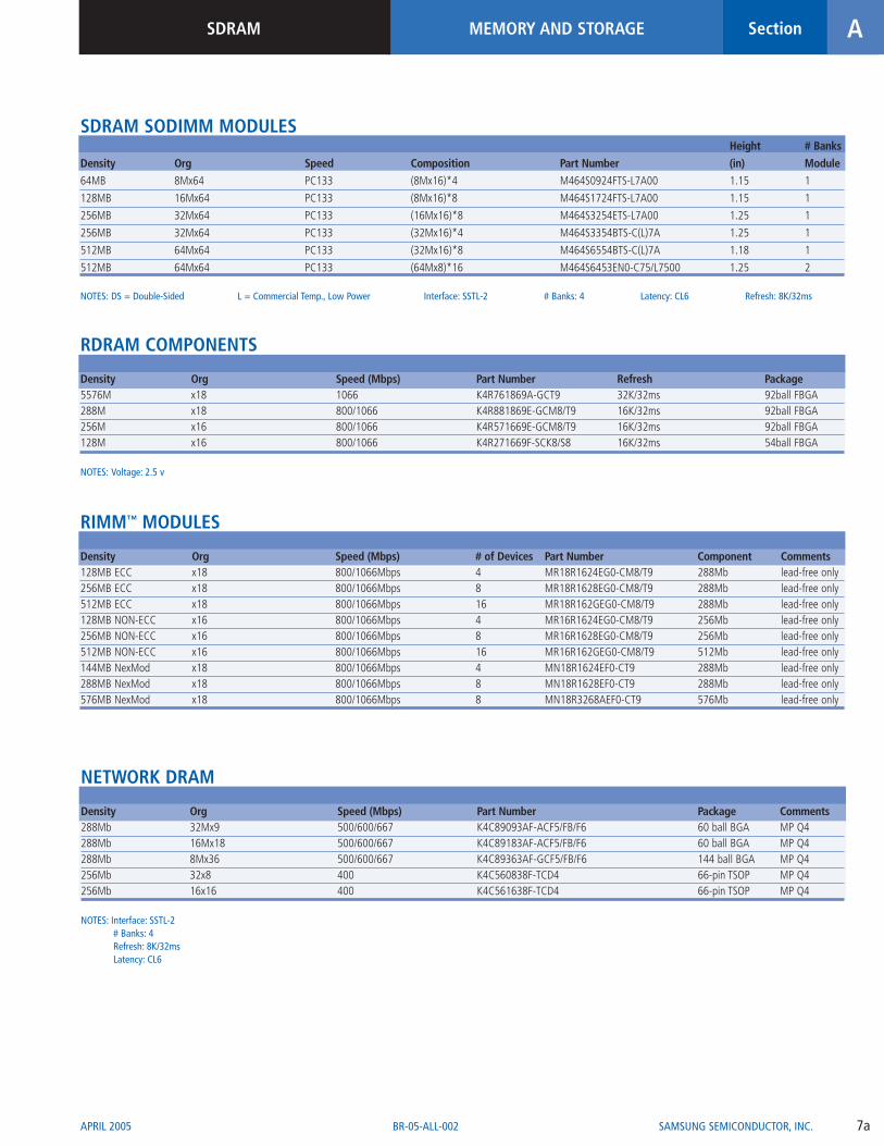
SDRAM SODIMM MODULES Height # Banks
Density Org Speed Composition Part Number (in) Module
64MB 8Mx64 PC133 (8Mx16)*4 M464S0924FTS-L7A00 1.15 1
128MB 16Mx64 PC133 (8Mx16)*8 M464S1724FTS-L7A00 1.15 1
256MB 32Mx64 PC133 (16Mx16)*8 M464S3254ETS-L7A00 1.25 1
256MB 32Mx64 PC133 (32Mx16)*4 M464S3354BTS-C(L)7A 1.25 1
512MB 64Mx64 PC133 (32Mx16)*8 M464S6554BTS-C(L)7A 1.18 1
512MB 64Mx64 PC133 (64Mx8)*16 M464S6453EN0-C75/L7500 1.25 2
NOTES: DS = Double-Sided L = Commercial Temp., Low Power Interface: SSTL-2 # Banks: 4 Latency: CL6 Refresh: 8K/32ms
RDRAM COMPONENTS
Density Org Speed (Mbps) Part Number Refresh Package5576M x18 1066 K4R761869A-GCT9 32K/32ms 92ball FBGA288M x18 800/1066 K4R881869E-GCM8/T9 16K/32ms 92ball FBGA256M x16 800/1066 K4R571669E-GCM8/T9 16K/32ms 92ball FBGA128M x16 800/1066 K4R271669F-SCK8/S8 16K/32ms 54ball FBGA
NOTES: Voltage: 2.5 v
RIMM™ MODULES
Density Org Speed (Mbps) # of Devices Part Number Component Comments128MB ECC x18 800/1066Mbps 4 MR18R1624EG0-CM8/T9 288Mb lead-free only256MB ECC x18 800/1066Mbps 8 MR18R1628EG0-CM8/T9 288Mb lead-free only512MB ECC x18 800/1066Mbps 16 MR18R162GEG0-CM8/T9 288Mb lead-free only128MB NON-ECC x16 800/1066Mbps 4 MR16R1624EG0-CM8/T9 256Mb lead-free only256MB NON-ECC x16 800/1066Mbps 8 MR16R1628EG0-CM8/T9 256Mb lead-free only512MB NON-ECC x16 800/1066Mbps 16 MR16R162GEG0-CM8/T9 512Mb lead-free only144MB NexMod x18 800/1066Mbps 4 MN18R1624EF0-CT9 288Mb lead-free only288MB NexMod x18 800/1066Mbps 8 MN18R1628EF0-CT9 288Mb lead-free only576MB NexMod x18 800/1066Mbps 8 MN18R3268AEF0-CT9 576Mb lead-free only
NETWORK DRAM
Density Org Speed (Mbps) Part Number Package Comments288Mb 32Mx9 500/600/667 K4C89093AF-ACF5/FB/F6 60 ball BGA MP Q4288Mb 16Mx18 500/600/667 K4C89183AF-ACF5/FB/F6 60 ball BGA MP Q4288Mb 8Mx36 500/600/667 K4C89363AF-GCF5/FB/F6 144 ball BGA MP Q4256Mb 32x8 400 K4C560838F-TCD4 66-pin TSOP MP Q4256Mb 16x16 400 K4C561638F-TCD4 66-pin TSOP MP Q4
NOTES: Interface: SSTL-2# Banks: 4Refresh: 8K/32msLatency: CL6

MOBILE SDRAM COMPONENTS# Pins
Density Org Part Number Refresh Power TSOP/BGA
64Mb 4Mx16 K4S641633H-(1)(2)(3)(4) 4K 3.0V FBGA-54balls64Mb 4Mx16 K4S64163LH-(1)(2)(3)(4) 4K 2.5V FBGA-54balls64Mb 4Mx16 K4M64163PH-(1)(2)(3)(4) 4K 1.8V FBGA-54balls64Mb 2MX32 K4S643233H-(1)(2)(3)(4) 4K 3.0V FBGA-90balls64Mb 2MX32 K4S64323LH-(1)(2)(3)(4) 4K 2.5V FBGA-90balls128Mb 8MX16 K4M281633F-(1)(2)(3)(4) 4K 3.0V FBGA-54balls128Mb 8MX16 K4M28163LF-(1)(2)(3)(4) 4K 2.5V FBGA-54balls128Mb 8MX16 K4M28163PF-(1)(2)(3)(4) 4K 1.8V FBGA-54balls128Mb 4MX32 K4S283233F-(1)(2)(3)(4) 4K 3.0V FBGA-90balls128Mb 4MX32 K4S28323LF-(1)(2)(3)(4) 4K 2.5V FBGA-90balls256Mb 16Mx16 K4S561633F-(1)(2)(3)(4) 8K 3.0V 54Balls BOC256Mb 16Mx16 K4S56163LF-(1)(2)(3)(4) 8K 2.5V 54Balls BOC256Mb 16Mx16 K4S56163PF-(1)(2)(3)(4) 4K 1.8V FBGA-54balls256Mb 8Mx32 K4S563233F-(1)(2)(3)(4) 4K 3.0V FBGA-90balls256Mb 8Mx32 K4S56323LF-(1)(2)(3)(4) 4K 2.5V FBGA-90balls256Mb 8Mx32 K4S56323PF-(1)(2)(3)(4) 4K 1.8V FBGA-90balls512Mb 32Mx16 K4S511533F-(1)(2)(3)(4) 8K 3.0V FBGA-54balls512Mb 32Mx16 K4S51153LF-(1)(2)(3)(4) 8K 2.5V FBGA-54balls512Mb 32Mx16 K4S511633F-(1)(2)(3)(4) 8K 3.0V FBGA-54balls512Mb 32Mx16 K4S51163LF-(1)(2)(3)(4) 8K 2.5V FBGA-54balls512Mb 32Mx16 K4S51163PF-(1)(2)(3)(4) 8K 1.8V FBGA-54balls512Mb 16Mx32 K4S513233F-(1)(2)(3)(4) 8K 3.0V FBGA-90balls512Mb 16Mx32 K4S51323LF-(1)(2)(3)(4) 8K 2.5V FBGA-90balls512Mb 16Mx32 K4S51323PF-(1)(2)(3)(4) 8K 1.8V FBGA-54balls
ASection MEMORY AND STORAGE
8a
Mobile SDRAM/Graphics DDR SDRAM
SAMSUNG SEMICONDUCTOR, INC. APRIL 2005
NOTES:Package:Leaded/Lead Free G / A: 52balls FBGA Mono R / B: 54balls FBGA Mono X / Z: 54balls BOC Mono J / V: 60(72)balls FBGA Mono
0.5pitch L / F: 60balls FBGA Mono 0.8pitch
S / D: 90balls FBGA Monolithic (11mm x 13mm)
F / H: Smaller 90balls FBGA Mono Y / P: 54balls CSP DDP M / E: 90balls FBGA DDP
Temp & Power:C: Commercial(-25 ~ 70’C), Normal L: Commercial, Low F: Commercial, Low, PASR & TCSR
B: Commercial, Super Low R: Commercial, Super Low,
PASR & TCSR E: Extended(-25~85’C), Normal N: Extended, Low G: Extended, Low, PASR & TCSR U: Extended, Super Low S: Extended, Super Low,
PASR & TCSR I : Industrial(-40~85’C), Normal
P: Industrial, Low H: Industrial, Low, PASR & TCSR D: Industrial, Super Low T: Industrial, Super Low,
PASR & TCSR
Speed:Mobile-SDRAM
60: 166MHz, CL 3 75: 133MHz, CL 3
80: 125MHz, CL 3 1H: 105MHz, CL 2 1L: 105MHz, CL 3 15: 66MHz, CL 2 & 3
Mobile-DDR C3: 133MHz, CL 3 C2: 100MHz, CL 3 C0: 66MHz, CL 3
BR-05-ALL-002
GRAPHICS DDR SDRAM COMPONENTS
Type Density Org Die Part Number Package VDD/VDDQ Speed Bin (MHz) Remarks
GDDR3 512Mb 16Mx32 C K4J52324Q 136 FBGA 1.8/1.8V 500/6002.0/2.0V 700/800
256Mb 8Mx32 F K4J55323Q 144 FBGA 2.0/2.0V 500/600/700/800 1.8V for GL20GDDR2 256Mb 16Mx16 F K4N56163Q 84 FBGA 1.8/1.8V 266/333/400/450GDDR1 256Mb 8Mx32 F' K4D553235 144 FBGA 1.8/1.8V 300/350
2.0/2.0V 4008Mx32 F' K4D553238 144 FBGA 2.5/2.5V 300/350/400/45016Mx16 F K4D551638 66 TSOPII 2.5/2.5V 200/250
2.8 ± 0.1V 2752.8 ~2.9V 300
128Mb 4Mx32 G K4D26323Q 144 FBGA 1.8/1.8V 300/350/400G K4D263238 144 FBGA 2.5/2.5V 300/350F K4D263238 100 TQFP 2.5/2.5V 200
8Mx16 F K4D261638 66 TSOPII 2.5/2.5V 200/250/275/300 CL-tRCD-tRP 3-4-4F K4D261638F-TC5A 2.55/2.55V 200Mhz for STB CL-tRCD-tRP 3-3-3
NOTES: * clock cycle time ** all products are 4 banks
Part No. Suffix 12 14 16 20 22 25 2A 33 36 37 40 50
Description 1.25ns 1.429ns 1.667ns 2.0 ns 2.2 ns 2.5 ns 2.86 NS 3.3 ns 3.6 ns 3.7 ns 4.0 ns 5.0 ns
(800MHz) (700MHz) (600MHz) (500MHz) (450MHz) (400MHz) (350MHz) (300MHZ) (275MHz) (266MHz) (250MHz) (200MHz)

9a
ASection MEMORY AND STORAGEDRAM Ordering Information
SAMSUNG SEMICONDUCTOR, INC.APRIL 2005 BR-05-ALL-002
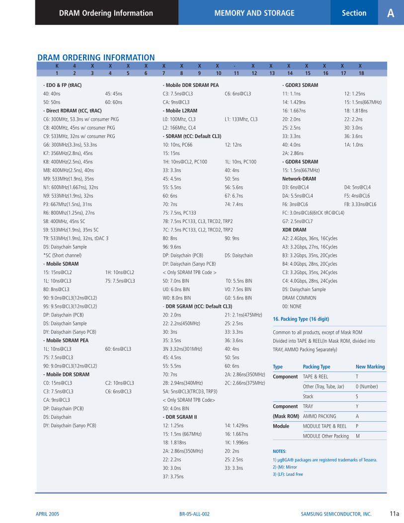
DRAM ORDERING INFORMATIONK 4 X X X X X X X X - X X X X X X X1 2 3 4 5 6 7 8 9 10 11 12 13 14 15 16 17 18
1. Memory (K)
2. DRAM:4
3. Small Classification
A:Advanced Dram Technology
B:DDR3 SDRAM
C: Network-DRAM
D: DDR SGRAM
E: EDO
F: FP
H: DDR SDRAM
J: GDDR3 SDRAM
K: Mobile SDRAM PEA
L: Mobile L2RAM
M: Mobile SDRAM
N: DDR SGRAM II
R: Direct RDRAM
S: SDRAM
T: DDR SDRAM II∫U: GDDR4 SDRAM
V: Mobile DDR SDRAM PEA
X: Mobile DDR SDRAM
Y: XDR DRAM
Z: Value Added DRAM
°∞ PEA: Power Efficient Address
4~5. Density, Refresh
111: 1G, 64K/16ms
15: 16M, 1K/16ms
16: 16M, 2K/32ms
17: 16M, 4K/64ms
26: 128M, 4K/32ms
27: 128M, 16K/32ms
28: 128M, 4K/64ms
32: 32M, 2K/32ms
40: 4M, 512/8ms
41: 4M, 1K/16ms
44: 144M, 16K/32ms
50: 512M, 32K/16ms
51: 512M, 8K/64ms
52: 512M, 8K/32ms
54: 256M, 16K/16ms
55: 256M, 4K/32ms
56: 256M, 8K/64ms
57: 256M, 16K/32ms
58: 256M, 8K/32ms
62: 64M, 2K/16ms
64: 64M, 4K/64ms
66: 64M, 8K/64ms
68: 768M, 8K/64ms
72: 72M, 8K/32ms
76: 576M, 32K/32ms
80: 8M, 2K/32ms
88: 288M, 16K/32ms
89: 288M, 8K/32ms
1G: 1G, 8K/64ms
2G: 2G, 8K/64ms
4G: 4G, 8K/64ms
2A: 128M, 4K/64ms with TCSR
5A: 256M, 8K/64ms with TCSR
6A: 64M, 4K/64ms with TCSR
6~7. Organization
01: x1 02: x2 03: x2 (Including x1)
04: x4 05: x4 (2CS)
06: x4 Stack (Flexframe)
07: x8 Stack (Flexframe)
08: x8 09: x9 15: x16 (2CS)
16: x16 17: x16 (Including x8/ x4)
18: x18 30: x32 (2CS, 2CKE)
31: x32 (2CS) 32: x32 36: x36
A8: x8 Stack (70-mono)
8. Bank
1: 1Bank 2: 2Bank 3: 4Bank
4: 8Bank 5: 16Bank 6: 32Bank
9. Interface,VDD,VDDQ
0: NONE, NONE, NONE
1: TTL, 5.0V, 5.0V
2: LVTTL, 3.3V, 3.3V
3: LVTTL, 3.0V, 3.0V
4: LVTTL, 2.5V, 2.5V
5: SSTL(LP), 1.8V, 1.8V
6: SSTL, 1.5V, 1.5V
7: SSTL-2, 3.3V, 2.5V
8: SSTL-2, 2.5V, 2.5V
9: RSL, 2.5V, 2.5V
A: SSTL, 2.5V, 1.8V
H: SSTL-2 DLL, 3.3V, 2.5V
J: LVTTL, 3.0V, 1.8V
L: LVTTL, 2.5V, 1.8V
M: LVTTL, 1.8V, 1.5V
N: LVTTL, 1.5V, 1.5V
P: LVTTL, 1.8V, 1.8V
Q: SSTL, 1.8V, 1.8V
R: SSTL-2, 2.8V, 2.8V
S: SSTL-2, 2.2V, 1.8V
U: DRSL, 1.8V, 1.2V
Y: SSTL(LP), 2.5V, 2.5V
10. Generation
M: 1st Generation
A: 2nd Generation
B: 3rd Generation
C: 4th Generation
D: 5th Generation
E: 6th Generation
F: 7th Generation
G: 8th Generation
H: 9th Generation
I: 10th Generation
J: 11th Generation
K: 12th Generation
Y: Partial DRAM(2nd)
Z: Partial DRAM (for RAMOSTAK Product)
11. “ ----”
12. Package
- Advanced DRAM Technology
G: WBGA L: TSOP2-400F(LF)
T: TSOP2 Z: BOC(LF)
- DDR SDRAM
J: TSOP2-400(LF, DDP) T: TSOP2-400
K: TSOP2-400(DDP) U: TSOP2-400(LF)
G: BOC, WBGA Z: BOC(LF)
P: BOC(DDP) Q: ISM
N: STSOP2 V: STSOP2(LF)
S: POP(DDP) X: POP(LF, DDP)
- DDR SDRAM II
G: BOC Z: BOC(LF)
S: BOC(Smaller) Y: BOC(Smaller, LF)
R: WLP
- DDR3 SDRAM
G: BOC Z: BOC(LF)
- DDR SGRAM
E: FBGA(LF, DDP) G : FBGA
J: FBGA(DDP) V: FBGA(LF)
P: FBGA(LLDDP) M: FBGA(1DQS)
N: FBGA(1DQS,LF) H: BOC
L: TSOP2-400(LF) T: TSOP2-400
Q: TQFP U: TQFP(LF)

ASection MEMORY AND STORAGE
10a
DRAM Ordering Information
SAMSUNG SEMICONDUCTOR, INC. APRIL 2005BR-05-ALL-002
DRAM ORDERING INFORMATIONK 4 X X X X X X X X - X X X X X X X1 2 3 4 5 6 7 8 9 10 11 12 13 14 15 16 17 18
- DDR SGRAM II
G: FBGA, BOC Z: BOC (LF)
- GDDR3 SDRAM
A: 136-FBGA, BOC B: 136-FBGA, BOC(LF)
G: FBGA, BOC V: FBGA, BOC(LF)
- Direct RDRAM
F: WBGA G: WBGA(LF)3)
H: WBGA(LF, B/ L 320) J: MWBGA(LF)
M: µBGA® packages1) (M)2)
N: µBGA® packages
P: MWBGA R: 54-WBGA
S: 54-µBGA® packages T: 54-WBGA(LF)
- EDO
B: SOJ-300 J: SOJ-400
N: STSOP2
T: TSOP2-400 U: TSOP2-400(LF)
F: TSOP2-300 H: TSOP2-300(LF)
- FP
B: SOJ-300 J: SOJ-400
F: TSOP2-300 H: TSOP2-300(LF)
N: STSOP2
T: TSOP2-400 U: TSOP2-400(LF)
- Mobile SDRAM
1: MCP 6: MCP(LF)
2: 90-FBGA(DDP) 3: 90-FBGA(DDP,LF)
4: 96-FBGA 5: 96-FBGA(LF)
R: 54-CSP B: 54-CSP(LF)
J: WBGA V: WBGA(LF)
M: FBGA(MCP) E: FBGA(LF, MCP)
F: Smaller 90 FBGA
H: Smaller 90 FBGA(LF)
Y: 54-CSP(DDP) P: 54-CSP(LF, DDP)
T: TSOP2-400 Q: ISM
S: 90-FBGA D: 90-FBGA(LF)
Mobile SDRAM PEA
F: Smaller 90-FBGA
H: Smaller 90-FBGA(LF)
S: 90-FBGA D: 90-FBGA(LF)
Mobile DDR SDRAM
1: MCP 6: MCP(LF)
4: 96-FBGA 5: 96-FBGA(LF)
7: 90-FBGA 8: 90-FBGA(LF)
F: WBGA(LF, 0.8MM) J: WBGA
L: WBGA(0.8MM) T: TSOP2
V: WBGA(LF) Q: ISM
S: POP X: POP(LF, DDP)
Mobile DDR SDRAM PEA
6: POP MONO(LF) 7: 90-FBGA
8: 90-FBGA(LF) F: 60-FBGA(LF)
L: 60-FBGA Q: ISM
S: POP(DDP) X: POP(LF, DDP)
Network-DRAM
A: 60-BOC B: 60-BOC(LF)
G: BOC Z: BOC(LF)
T: TSOP2 U: TSOP2(LF)
XDR DRAM
J: BOC(LF) P: BOC
SDRAM
1: MCP 2: 90-FBGA(DDP)
3: 90-FBGA(DDP, LF) 4: 96-FBGA
5: 96-FBGA(LF) A: 52-CSP(LF)
G: CSP(except 54 Pin) R: 54-CSP
B: 54-CSP(LF) D: 90-FBGA(LF)
E: 90-FBGA (LF, MCP) S: 90-FBGA
M: 90-FBGA(MCP) F: Smaller 90FBGA
H: Smaller 90FBGA(LF) K: TSOP2-400(DDP)
N: STSOP2 V: STSOP2(LF)
T: TSOP2-400 U: TSOP2-400(LF)
Y: 54-CSP(DDP) P: 54-CSP(LF, DDP)
X: BOC Z: BOC(LF)
DRAM COMMON
C: CHIP BIZ W: WAFER
(M): Mirror (LF): Lead Free
13. Temp, Power
- COMMON (Temp, Power)
0: NONE, NONE
A: Automotive, Normal
C: Commercial, Normal
J: Commercial, Medium
L: Commercial, Low
F: Commercial, Low, PASR & TCSR
B: Commercial, Super Low
R: Commercial, Super Low, PASR & TCSR
K: Commercial, Reduced
E: Extended, Normal
N: Extended, Low
G: Extended, Low, PASR & TCSR
U: Extended, Super Low
S: Extended, Super Low, PASR & TCSR
X: Extra Extend, Normal
I: Industrial, Normal
P: Industrial, Low
H: Industrial, Low, PASR & TCSR
D: Industrial, Super Low
T: Industrial, Super Low, PASR & TCSR
- WAFER,CHIP BIZ Level Classification
0: NONE, NONE
1: DC test only
2: DC test, WBI
3: DC, several AC test, WBI
14~15. Speed (Wafer/Chip Biz/BGD: 00)
- DDR SDRAM
A0: 10ns@CL2 A1: 8ns
A2: 7.5ns@CL2
AA :7.5ns@CL2,TRCD2,TRP2
B0: [email protected] B3: [email protected]
B4: [email protected] C3: 6ns@CL3
C4: 5ns@CL3 C5: 3.75ns@CL3
CA: 5.5ns@CL3
CC: 5ns@CL3,TRCD3,TRP3 CD: 4ns@CL3
CE: 5ns@CL3, TRCD3, TRPS3(2.5V)
D4: 5ns@CL4 DS: Daisychain
<Only DDR SDRAM TPB code>
S0: SH BIN(TPB) V0: SH 2/ 2/ 2 BIN
W0: SH 3/ 3/ 3 BIN X0: Uniq. BIN
Y0: SH 3/ 4/ 4 BIN
- DDR SDRAM II
C4: 5ns@CL3 C5: 3.75ns@CL3
CC: 5ns@CL3,TRCD3,TRP3
CF: 3.75ns@CL3(1.9V)
D4: 5ns@CL4 D5: 3.75ns@CL4
D6: 3.0ns@CL4 D7: 2.5ns@CL4
DH: 3ns@CL4(1.9V)
DS: Daisychain Sample E4: 5ns@CL5
E5: 3.75ns@CL5 E6: 3.0ns@CL5
E7: 2.5ns@CL5 F6: 3.0ns@CL6
F7: 2.5ns@CL6
- DDR3 SDRAM
E7: 2.5ns@CL5 F6: 3.0ns@CL6
F7: 2.5ns@CL6
ASection MEMORY AND STORAGE
11a
DRAM Ordering Information
SAMSUNG SEMICONDUCTOR, INC.APRIL 2005 BR-05-ALL-002
DRAM ORDERING INFORMATION K 4 X X X X X X X X - X X X X X X X1 2 3 4 5 6 7 8 9 10 11 12 13 14 15 16 17 18
- EDO & FP (tRAC)
40: 40ns 45: 45ns
50: 50ns 60: 60ns
- Direct RDRAM (tCC, tRAC)
C6: 300MHz, 53.3ns w/ consumer PKG
C8: 400MHz, 45ns w/ consumer PKG
C9: 533MHz, 32ns w/ consumer PKG
G6: 300MHz(3.3ns), 53.3ns
K7: 356MHz(2.8ns), 45ns
K8: 400MHz(2.5ns), 45ns
M8: 400MHz(2.5ns), 40ns
M9: 533MHz(1.9ns), 35ns
N1: 600MHz(1.667ns), 32ns
N9: 533MHz(1.9ns), 32ns
P3: 667Mhz(1.5ns), 31ns
R6: 800Mhz(1.25ns), 27ns
S8: 400MHz, 45ns SC
S9: 533MHz(1.9ns), 35ns SC
T9: 533MHz(1.9ns), 32ns, tDAC 3
DS: Daisychain Sample
*SC (Short channel)
- Mobile SDRAM
15: 15ns@CL2 1H: 10ns@CL2
1L: 10ns@CL3 75: 7.5ns@CL3
80: 8ns@CL3
90: 9.0ns@CL3(12ns@CL2)
95: 9.5ns@CL3(12ns@CL2)
DP: Daisychain (PCB)
DS: Daisychain Sample
DY: Daisychain (Sanyo PCB)
- Mobile SDRAM PEA
1L: 10ns@CL3 60: 6ns@CL3
75: 7.5ns@CL3
90: 9.0ns@CL3(12ns@CL2)
- Mobile DDR SDRAM
C0: 15ns@CL3 C2: 10ns@CL3
C3: 7.5ns@CL3 C6: 6ns@CL3
CA: 9ns@CL3
DP: Daisychain (PCB)
DS: Daisychain
DY: Daisychain (Sanyo PCB)
- Mobile DDR SDRAM PEA
C3: 7.5ns@CL3 C6: 6ns@CL3
CA: 9ns@CL3
- Mobile L2RAM
L0: 100Mhz, CL3 L1: 133Mhz, CL3
L2: 166Mhz, CL4
- SDRAM (tCC: Default CL3)
10: 10ns, PC66 12: 12ns
15: 15ns
1H: 10ns@CL2, PC100 1L: 10ns, PC100
33: 3.3ns 40: 4ns
45: 4.5ns 50: 5ns
55: 5.5ns 56: 5.6ns
60: 6ns 67: 6.7ns
70: 7ns 74: 7.4ns
75: 7.5ns, PC133
7B: 7.5ns PC133, CL3, TRCD2, TRP2
7C: 7.5ns PC133, CL2, TRCD2, TRP2
80: 8ns 90: 9ns
96: 9.6ns
DP: Daisychain (PCB) DS: Daisychain
DY: Daisychain (Sanyo PCB)
< Only SDRAM TPB Code >
S0: 7.0ns BIN T0: 5.5ns BIN
U0: 6.0ns BIN V0: 7.5ns BIN
W0: 8.0ns BIN G0: 5.6ns BIN
- DDR SGRAM (tCC: Default CL3)
20: 2.0ns 21: 2.1ns(475MHz)
22: 2.2ns(450MHz) 25: 2.5ns
30: 3ns 33: 3.3ns
35: 3.5ns 36: 3.6ns
3N 3.32ns(301MHz) 40: 4ns
45: 4.5ns 50: 5ns
55: 5.5ns 60: 6ns
70: 7ns 2A: 2.86ns(350MHz)
2B: 2.94ns(340MHz) 2C: 2.66ns(375MHz)
5A: 5ns@CL3(TRCD3, TRP3)
< Only SDRAM TPB Code>
S0: 4.0ns BIN
- DDR SGRAM II
12: 1.25ns 14: 1.429ns
15: 1.5ns (667MHz) 16: 1.667ns
18: 1.818ns 1K: 1.996ns
2A: 2.86ns(350MHz) 20: 2ns
22: 2.2ns 25: 2.5ns
30: 3.0ns 33: 3.3ns
37: 3.75ns
- GDDR3 SDRAM
11: 1.1ns 12: 1.25ns
14: 1.429ns 15: 1.5ns(667MHz)
16: 1.667ns 18: 1.818ns
20: 2.0ns 22: 2.2ns
25: 2.5ns 30: 3.0ns
33: 3.3ns 36: 3.6ns
40: 4.0ns 1A: 1.0ns
2A: 2.86ns
- GDDR4 SDRAM
15: 1.5ns(667MHz)
Network-DRAM
D3: 6ns@CL4 D4: 5ns@CL4
DA: 5.5ns@CL4 F5: 4ns@CL6
F6: 3ns@CL6 FB: 3.33ns@CL6
FC: 3.0ns@CL6(6tCK tRC@CL4)
G7: 2.5ns@CL7
XDR DRAM
A2: 2.4Gbps, 36ns, 16Cycles
A3: 3.2Gbps, 27ns, 16Cycles
B3: 3.2Gbps, 35ns, 20Cycles
B4: 4.0Gbps, 28ns, 20Cycles
C3: 3.2Gbps, 35ns, 24Cycles
C4: 4.0Gbps, 28ns, 24Cycles
DS: Daisychain Sample
DRAM COMMON
00: NONE
16. Packing Type (16 digit)
Common to all products, except of Mask ROM
Divided into TAPE & REEL(In Mask ROM, divided into
TRAY, AMMO Packing Separately)
Type Packing Type New Marking
Component TAPE & REEL T
Other (Tray, Tube, Jar) 0 (Number)
Stack S
Component TRAY Y
(Mask ROM) AMMO PACKING A
Module MODULE TAPE & REEL P
MODULE Other Packing M
NOTES:
1) µgBGA® packages are registered trademarks of Tessera.
2) (M): Mirror
3) (LF): Lead Free

ASection MEMORY AND STORAGE
12a
Flash
SAMSUNG SEMICONDUCTOR, INC. APRIL 2005BR-05-ALL-002
NAND FLASH DISCRETE COMPONENTSSpeed
Density Part Number Organization (ns) Voltage Package128Mb K9F2808U0C-PCB 16Mx8 50 3.3V TSOP48256Mb K9F5608U0C-PCB 32Mx8 50 3.3V TSOP48512Mb K9F1208U0B-PCB 64Mx8 50 3.3V TSOP481Gb K9F1G08U0A-PCB 128Mx8 50 3.3V TSOP482Gb K9F2G08U0M-PCB 256Mx8 30 3.3V TSOP484Gb K9K4G08U0M-PCB 512Mx8 30 3.3V TSOP488Gb K9W8G08U1M-PCB 1024Mx8 30 3.3V TSOP48
NOTE: All parts lead free
NOR FLASH
Density TSOP Part Number FBGA Part Number Block Architecture Voltage16Mb K8D1716UTC-PI07 K8D1716UTC-FI07 Top 3.3V
K801716UBC-PI07 K8D1716UBC-FI07 Bottom 3.3V32Mb K8D3216UTC-PI07 N/A Top 3.3V
K8D3216UBC-PI07 N/A Bottom 3.3V64Mb K8D6316UTM-PI07 N/A Top 3.3V
K8D6316UBM-PI07 N/A Bottom 3.3V
NOTE: All parts lead free
OneNAND™ FLASH
Density Part Number Package Organization Voltage(V) Temperature128Mb KFG2816Q1M-PEB0000 48 TSOP X16 1.8v Extended
KFG2816D1M-PEB0000 <Pb free> " 2.7v ExtendedKFG2816U1M-PIB0000 " 3.3v Industrial
256Mb KFG5616Q1M-PEB0000 48 TSOP X16 1.8v ExtendedKFG5616D1M-PEB0000 <Pb free> " 2.7v ExtendedKFG5616U1M-PIB0000 " 3.3v IndustrialKFG5616Q1M-DEB0000 63 FBGA X16 1.8v ExtendedKFG5616D1M-DEB0000 <Pb free> " 2.7v ExtendedKFG5616U1M-DIB0000 " 3.3v Industrial
512Mb KFG1216Q2M-DEB0000 63 FBGA X16 1.8v ExtendedKFG1216D2M-DEB0000 <Pb free> " 2.7v ExtendedKFG1216U2M-DIB0000 " 3.3v Industrial
1Gb KFG1G16Q2M-DEB0000 63 FBGA X16 1.8v ExtendedKFG1G16D2M-DEB0000 <Pb free> " 2.7v ExtendedKFG1G16U2M-DIB0000 " 3.3v Industrial

APRIL 2005 BR-05-ALL-002
ASection MEMORY AND STORAGE
13a
NAND Flash Ordering Information
SAMSUNG SEMICONDUCTOR, INC.
NAND FLASH ORDERING INFORMATIONK 4 X X X X X X X X - X X X X X X X1 2 3 4 5 6 7 8 9 10 11 12 13 14 15 16 17 18
1. Memory (K)
2. NAND Flash: 9
3. Small Classification (SLC: Single Level Cell, MLC:Multi Level Cell, SM: SmartMedia, S/B: Small Block)
A: SLC + Muxed I/F ChipB: Muxed I/F ChipS: SLC Single SMD: SLC Dual SMQ: 4CHIP SMT: SLC SINGLE (S/B)E: SLC DUAL (S/B)R: SLC 4DIE STACK (S/B)F: SLC NormalG: MLC NormalK: SLC 2-Die StackW: SLC 4-Die StackJ: Non-Muxed OneNANDU: 2 STACK MSPV: 4 STACK MSP
4~5. Density
12: 512M 16: 16M28: 128M 32: 32M40: 4M 56: 256M 64: 64M 80: 8M1G: 1G 2G: 2G4G: 4G 8G: 8G00: NONE
6~7. Organization
00: NONE 08: x816: x16
8. Vcc
C: 5.0V(4.5V~5.5V) D: 2.65V(2.4V~2.9V) E: 2.3V~3.6V Q: 1.8V(1.7V~1.95V) T: 2.4V~3.0V U: 2.7V~3.6V V: 3.3V(3.0V~3.6V) W: 2.7V~5.5V,3.0V~5.5V 0: NONE
9. Mode
O: Normal 1: Dual nCE & Dual Rn/B 4: Quad nCE & Single RnB A: Mask Option 1
10. Generation
M: 1st GenerationA: 2nd GenerationB: 3rd GenerationC: 4th GenerationD: 5th GenerationY: Partial NAND(2nd)Z: Partial NAND(1st)M: 1st GenerationA: 2nd GenerationB: 3rd GenerationC: 4th GenerationD: 5th GenerationY: Partial NAND(2nd)Z: Partial NAND(1st)
11. “--”
12. Package
A: COB B: TBGAC: CHIP BIZ D: 63-TBGAE: TSOP1(LF,1217) F: WSOP1(LF)G: FBGA H: TBGA(LF)J: FBGA(LF) K: TSOP1(1217)L: LGA M: tLGAP: TSOP1(LF) Q: TSOP2(LF) R: TSOP2-R S: SMARTMEDIAT: TSOP2 V: WSOPW: WAFER Y: TSOP1
13. Temp
C: Commercial I: Industrial0: NONE
14. Bad Block
B: Include Bad BlockD: Daisychain Sample L: 1~5 Bad BlockN: Ini. All Good, Add. 10 BlocksS: All Good Block0: NONE
15. NAND-Reserved
0: Reserved
16. Packing Type (16 digit)
Common to all products, except of Mask ROM
Divided into TAPE & REEL(In Mask ROM, divided into
TRAY, AMMO Packing Separately)
Type Packing Type New Marking
Component TAPE & REEL T
Other (Tray, Tube, Jar) 0 (Number)
Stack S
Component TRAY Y
(Mask ROM) AMMO PACKING A
Module MODULE TAPE & REEL P
MODULE Other Packing M

ASection MEMORY AND STORAGE
14a
SRAM
SAMSUNG SEMICONDUCTOR, INC. APRIL 2005BR-05-ALL-002
LOW-POWER (5V) SRAMOperating Operating Standby Production
Density Part Number Organization Vcc (V) Speed(ns) Temp Current (mA) Current (uA) Package Status
8Mbit K6X8008C2B 1Mx8 4.5 - 5.5 55,70 C,I 50 50 TSOP2(44) Mass Production
K6X8016C3B 512x16 4.5 - 5.5 55,70 C,I 60 50 TSOP2(44) Mass Production4Mbit K6X4016C3F 256x16 4.5 - 5.5 55,70 I,A 50 20,30 TSOP2(44) Mass Production
K6X4008C1F 512x8 4.5 - 5.5 55,70 I,A 40 20,30 32SOP,TSOP Mass Production1Mbit K6T1008C2E 128x8 4.5 - 5.5 55,70 C,I 50 10 32DIP,32SOP,TSOP1(32) EOL
K6X1008C2D 128x8 4.5 - 5.5 55,70 I,A 35 15,25 32SOP,TSOP1(32) Mass Production256K bit K6T0808C1D 32x8 4.5 - 5.5 55,70 C,I 60 5 28SOP,TSOP1(28) EOL
K6X0808C1D 32x8 4.5 - 5.5 55,70 C,I 35 25 28SOP Mass Production
NOTE: Lead-free available upon request
LOW-VOLTAGE & LOW-POWER SRAMOperating Operating Standby Production
Density Part Number Organization Vcc (V) Speed (ns) Temp Current (mA) Current (uA) Package Status8Mbit K6X8008T2B 1024Kx8 2.7 - 3.6 55,70 C,I 40 40 TSOP2(44) Mass Production
K6X8016T3B 512Kx16 2.7 - 3.6 55,70 C,I 45 40 TSOP2(44) Mass Production4Mbit K6X4008T1F 512x8 2.7 - 3.6 70,85 I,A 30 20,30 32SOP,TSOP2(32) Mass Production
K6X4016T3F 256x16 2.7 - 3.6 70,85 I,A 40 20,30 TSOP2(44) Mass Production1Mbit K6F1008U2C 128x8 2.7 - 3.3 55,70 I 2 0.5 32TSOP1 Mass Production
K6X1008T2D 128x8 2.7 - 3.6 70,85 I,A 25 10,20 32SOP,TSOP2(32) Mass ProductionK6F1008V2C 128x8 3.0 - 3.6 55,70 I 3 0.5 25SOP1 Mass Production
MICRO-POWER & LOW-VOLTAGE SRAMOperating Operating Standby Production
Density Part Number Organization Vcc (V) Speed (ns) Temp Current (mA) Current (uA) Package Status16Mbit K6F1616U6C 1x16 2.7 - 3.3 55,70 I 3 1 48-FBGA Mass Production
K6F1616R6C 1x16 1.65 - 2.2 70 I 3 1 48-FBGA Mass Production8Mbit K6F8016R6B 512x16 1.65 - 2.2 70,85 I 3 1 48-TBGA EOL
K6F8016U6B 512x16 2.7 - 3.3 55,70 I 4 1 48-TBGA EOL4Mbit K6F4008R2G 512Kx8 1.65 - 2.20 70,85 I 2 0.5 36TBGA Mass Production
K6F4008U2G 512Kx8 2.7 - 3.3 45,55,70 I 2 0.5 36TBGA Mass ProductionK6F4016R4E 256Kx16 1.65 - 2.20 70, 85 I 2 0.5 48TBGA Mass ProductionK6F4016R6G 256Kx16 1.65 - 2.20 70,85 I 2 0.5 48TBGA Mass ProductionK6F4016U4G 256Kx16 2.7 - 3.3 55,70 I 2 0.5 48TBGA Mass ProductionK6F4016U6G 256Kx16 2.7 - 3.3 55,70 I 2 0.5 48TBGA Mass Production
2Mbit K6F2016U4E 128x16 2.7 - 3.3 55,70 I 2 0.5 48-TBGA Mass ProductionK6F2016R4E 128x16 1.65 - 2.2 70,85 I 2 0.5 48-FBGA Mass ProductionK6F2008U2E 256x8 2.7 - 3.3 55,70 I 2 0.5 32TSOP1 Mass ProductionK6F2008V2E 256x8 3.0 - 3.6 55,70 I 3 0.5 32TSOP1 Mass Production
1Mbit K6F1016U4C 64x16 2.7 - 3.3 55,70 I 2 0.5 48-FBGA Mass Production

ASection MEMORY AND STORAGE
15a
SRAM
SAMSUNG SEMICONDUCTOR, INC.APRIL 2005 BR-05-ALL-002
UtRAM (HIGH DENSITY & LOW POWER)Operating Operating Standby
Density Part Number Organization Vcc (V) Speed (ns) Temp Current (mA) Current (uA) Package Production Status32Mbit K1S321615M 2Mx16 3 100 E 20 150 48-TBGA EOL
K1S321611C 2Mx17 3 70 I 35 100 48-FBGA Mass ProductionK1S321615A 2Mx16 3 85 E 35 100 48-TBGA Mass Production
16Mbit K1S161615M 1Mx16 3 70 I 20 70 48-TBGA Mass ProductionK1S1616B1M 1Mx16 1.8 70 I 35 60 48-TBGA Mass Production
HIGH-SPEED (4Mbit) ASYNCHRONOUS FAST SRAMOperating Operating Standby Production
Density Part Number Organization Vcc (V) Speed (ns) Temp Current (mA) Current (uA) Package Status4Mbit 4K6R4016C1D 256Kx16 5 10, 12 C,I 65, 55 20, 5 44SOJ, 44TSOP2, 48TBGA Mass Production
K6R4016V1D 256Kx16 3.3 8, 10 C,L,I,P 80, 65 20, 5(1.2) 44SOJ, 44TSOP2, 48TBGA Mass ProductionK6R4004C1D 1Mx4 5 10, 12 C,I 65, 55 20, 5 32 SOJ Mass ProductionK6R4004V1D 1Mx4 3.3 8, 10 C,I 80, 65 20, 5 32 SOJ Mass ProductionK6R4008C1D 512Kx8 5 10, 12 C,I,P 65, 55 20, 5 36 SOJ, 44 TSOP2 Mass ProductionK6R4008V1D 512Kx8 3.3 8, 10 C,I 80, 65 20, 5 36 SOJ, 44 TSOP2 Mass Production
3Mbit K6R3024V1D 128x24 3.3 9, 10, 12 C,I 170,150,130 40,15 119PBGA Mass Production1Mbit K6R1008V1D 128x8 3.3 8, 10, 12 C,I 170,150,130 20,5 32SOJ,32TSOP2 Mass Production
K6R1008C1D 128x8 5 10, 12, 15 C,I 170,150,130 20,5 32SOJ,32TSOP2 Mass ProductionK6R1004V1D 256x4 3.3 8, 10, 12 C,I 170,150,130 20,5 32SOJ Mass ProductionK6R1004C1D 256x4 5 10, 12, 15 C,I 170,150,130 20,5 32SOJ Mass ProductionK6R1016V1D 64x16 3.3 8, 10, 12 C,I 170,150,130 20,5 44SOJ,44TSOP2,48TBGA Mass ProductionK6R1016C1D 64x16 5 10, 12, 15 C,I 170,150,130 20,5 44SOJ,44TSOP2,48TBGA Mass Production
SPB & FT (36Mbit) SRAMPart Operating Access Time Speed I/O Production Number Organization Mode Vdd (V) tCD(ns) tCYC (MHz) Voltage (V) Package Status CommentsK7A323600M 1Mx36 SPB 3.3 2.6, 3.1, 4.0 250, 200, 138 3.3, 2.5 100TQFP Mass Production 2E1DK7A321800M 2Mx18 SPB 3.3 2.6, 3.1, 4.0 250, 200, 138 3.3, 2.5 100TQFP Mass Production 2E1DK7B323625M 1Mx36 SB 3.3 6.5, 7.5 133, 118, 100 3.3, 2.5 100TQFP Mass Production - K7B321825M 2Mx18 SB 3.3 6.5, 7.5 133, 118, 100 3.3, 2.5 100TQFP Mass Production -
NOTES: 2E1D = 2-cycle Enable and 1-cycle Disable
SPB & FT (18Mbit) SRAMPart Operating Access Time Speed I/O Production Number Organization Mode Vdd (V) tCD (ns) tCYC (MHz) Voltage (V) Package Status CommentsK7A163600A 512Kx36 SPB 3.3 2.6, 3.5, 4.0 250, 167, 138 3.3, 2.5 100TQFP EOL 2H`05 2E1DK7A163601A 512Kx36 SPB 3.3 3.1, 3.5 200, 167 3.3, 2.5 100TQFP EOL 2H`05 2E2DK7A161800A 1Mx18 SPB 3.3 2.6, 3.5, 4.0 250, 167, 138 3.3, 2.5 100TQFP EOL 2H`05 2E1DK7A161801A 1Mx18 SPB 3.3 3.1, 3.5 200, 167 3.3, 2.5 100TQFP EOL 2H`05 2E2DK7B163625A 512Kx36 SB 3.3 7.5, 8.5 118, 100 3.3, 2.5 100TQFP EOL 2H`05 - K7B161825A 1Mx18 SB 3.3 7.5, 8.5 118, 100 3.3, 2.5 100TQFP EOL 2H`05 - K7A163630B 512Kx36 SPB 3.3, 2.5 2.6, 3.5 250, 167 3.3, 2.5 100TQFP Mass Production 4Q`05 2E1DK7A163631B 512Kx36 SPB 3.3, 2.5 3.1 200 3.3, 2.5 100TQFP Mass Production 4Q`05 2E2DK7A161830B 1Mx18 SPB 3.3, 2.5 2.6, 3.5 250, 167 3.3, 2.5 100TQFP Mass Production 4Q`05 2E1DK7A161831B 1Mx18 SPB 3.3, 2.5 3.1 200 3.3, 2.5 100TQFP Mass Production 4Q`05 2E2DK7B163635B 512Kx36 SB 3.3, 2.5 7.5 118 3.3, 2.5 100TQFP Mass Production 4Q`05 - K7B161835B 1Mx18 SB 3.3, 2.5 7.5 118 3.3, 2.5 100TQFP Mass Production 4Q`05 -
NOTES: 2E1D = 2-cycle Enable and 1-cycle Disable 2E2D = 2-cycle Enable and 2-cycle Disable

ASection MEMORY AND STORAGE
16a
SRAM
SAMSUNG SEMICONDUCTOR, INC. APRIL 2005BR-05-ALL-002
SPB & FT (8Mbit) SRAMPart Operating Access Time Speed I/O Production Number Organization Mode Vdd (V) tCD(ns) tCYC (MHz) Voltage (V) Package Status Comments
K7A803600B 256x36 SPB 3.3 3.5,3.8 167,138 3.3,2.5 100TQFP Mass Production 2E1DK7A803609B 256x36 SPB 3.3 2.6 250 3.3,2.5 100TQFP Mass Production 2E1DK7A801800B 512x18 SPB 3.3 3.5,3.8 167,138 3.3,2.5 100TQFP Mass Production 2E1DK7A801809B 512x18 SPB 3.3 2.6 250 3.3,2.5 100TQFP Mass Production 2E1DK7B803625B 256x36 SB 3.3 6.5,7.5 133,117 3.3,2.5 100TQFP Mass Production - K7B801825B 512x18 SB 3.3 6.5,7.5 133,117 3.3,2.5 100TQFP Mass Production -
NOTES: 2E1D = 2-cycle Enable and 1-cycle Disable Recommended speed options for SPB are 250MHz and 167MHz.2E2D = 2-cycle Enable and 2-cycle Disable Recommended access speed option for SB is 6.5ns.
SPB & FT (4Mbit) SRAMPart Operating Access Time Speed I/O Production Number Organization Mode Vdd (V) tCD(ns) tCYC (MHz) Voltage (V) Package Status CommentsK7A403600B 128Kx36 SPB 3.3 3.5, 4.0 167, 138 3.3, 2.5 100 TQFP Mass Production 2E1DK7A401800B 256Kx18 SPB 3.3 3.5, 4.0 167, 138 3.3, 2.5 100 TQFP Mass Production 2E1DK7A403609B 128Kx36 SPB 3.3 2.4, 2.8 250, 200 3.3, 2.5 100 TQFP Mass Production 2E1DK7A401809B 256Kx18 SPB 3.3 2.4, 2.8 250, 200 3.3, 2.5 100 TQFP Mass Production 2E1DK7A403200B 128Kx32 SPB 3.3 3.5, 4.0 167, 138 3.3, 2.5 100 TQFP Mass Production 2E1DK7B403625B 128Kx36 SB 3.3 6.5, 7.5 133, 118 3.3, 2.5 100 TQFP Mass ProductionK7B401825B 256Kx18 SB 3.3 6.5, 7.5 133, 118 3.3, 2.5 100 TQFP Mass Production
NOTES: 2E1D = 2-cycle Enable and 1-cycle Disable Recommended speed options for SPB are 250MHz and 167MHz.2E2D = 2-cycle Enable and 2-cycle Disable Recommended access speed option for SB is 6.5ns.
SPB & FT (36Mbit) NTRAMPart Operating Access Time Speed I/O Production Number Organization Mode Vdd (V) tCD(ns) tCYC (MHz) Voltage (V) Package StatusK7N323645M 1Mx36 SPB 2.5 2.6, 3.2,3.5,4.2 250, 200,167, 133 2.5 100TQFP, 165FBGA Mass Production K7N321845M 2Mx18 SPB 2.5 2.6, 3.2,3.5,4.2 250, 200,167, 133 2.5 100TQFP, 165FBGA Mass Production K7N323601M 1Mx36 SPB 3.3 2.6, 3.2,3.5,4.2 250, 200,167, 133 3.3, 2.5 100TQFP, 165FBGA Mass Production K7N321801M 2Mx18 SPB 3.3 2.6, 3.2,3.5,4.2 250, 200,167, 133 3.3, 2.5 100TQFP, 165FBGA Mass Production K7M323625M 1Mx36 FT 3.3 7.5 118 3.3, 2.5 100TQFP Mass Production K7M321825M 2Mx18 FT 3.3 7.5 118 3.3, 2.5 100TQFP Mass Production
NOTES: Recommended speed options for SPB are 250MHz, 200MHz and 167MHz. Recommended access speed option for SB is 7.5ns.
SPB & FT (2Mbit) SRAMPart Operating Access Time Speed I/O Production Number Organization Mode Vdd (V) tCD(ns) tCYC (MHz) Voltage (V) Package Status Comments
K7A203600B 64Kx36 SPB 3.3 4 138 2.5, 3.3 100 TQFP Mass Production 2E1D
K7A203200B 64Kx32 SPB 3.3 4 138 2.5, 3.3 100 TQFP Mass Production 2E1D
NOTES: 2E1D = 2-cycle Enable and 1-cycle Disable 2E2D = 2-cycle Enable and 2-cycle Disable
SPB & FT (18Mbit) NTRAM Part Operating Access Time Speed I/O Production Number Organization Mode Vdd (V) tCD(ns) tCYC (MHz) Voltage (V) Package StatusK7N161801A 1Mx18 SPB 3.3 2.6, 3.2, 3.5, 4.2 250, 200, 167, 133 3.3, 2.5 100TQFP, 165FBGA EOL 2H`05K7N163601A 512Kx36 SPB 3.3 2.6, 3.2, 3.5, 4.2 250, 200, 167, 133 3.3, 2.5 100TQFP, 165FBGA EOL 2H`05K7N163645A 512Kx36 SPB 2.5 2.6, 3.2, 3.5, 4.2 250, 200, 167, 133 2.5 100TQFP, 165FBGA EOL 2H`05K7N161845A 1Mx18 SPB 2.5 2.6, 3.2, 3.5, 4.2 250, 200, 167, 133 2.5 100TQFP, 165FBGA EOL 2H`05K7M161825A 1Mx18 FT(SB) 3.3 6.5, 7.5 133, 117 3.3, 2.5 100TQFP EOL 2H`05K7M163625A 512Kx36 FT(SB) 3.3 6.5, 7.5 133, 117 3.3, 2.5 100TQFP EOL 2H`05K7N161831B 1Mx18 SPB 3.3, 2.5 2.6, 3.2, 3.5 250, 200, 167 3.3, 2.5 100TQFP, 165FBGA Mass Production Q4`05K7N163631B 512Kx36 SPB 3.3, 2.5 2.6, 3.2, 3.5 250, 200, 167 3.3, 2.5 100TQFP, 165FBGA Mass Production Q4`05K7M161835B 1Mx18 FT(SB) 3.3 6.5 133 3.3, 2.5 100TQFP Mass Production Q4`05K7M163635B 512Kx36 FT(SB) 3.3 6.5 133 3.3, 2.5 100TQFP Mass Production Q4`05
NOTE: B-version samples are available now.

ASection MEMORY AND STORAGE
17a
SRAM
SAMSUNG SEMICONDUCTOR, INC.APRIL 2005 BR-05-ALL-002
SPB & FT (8Mbit) NtRAM Part Operating Access Time Speed I/O Production Number Organization Mode Vdd (V) tCD(ns) tCYC (MHz) Voltage (V) Package StatusK7N803601B 256Kx36 SPB 3.3 3.5, 4.2 167,133 3.3,2.5 100TQFP Mass ProductionK7N801801B 512Kx18 SPB 3.3 3.5, 4.2 167,133 3.3,2.5 100TQFP Mass ProductionK7N803609B 256Kx36 SPB 3.3 2.6 250 3.3,2.5 100TQFP Mass ProductionK7N801809B 512Kx18 SPB 3.3 2.6 250 3.3,2.5 100TQFP Mass ProductionK7N803645B 256Kx36 SPB 2.5 3.5, 4.2 167,133 2.5 100TQFP Mass ProductionK7N801845B 512Kx18 SPB 2.5 3.5, 4.2 167,133 2.5 100TQFP Mass ProductionK7N803649B 256Kx36 SPB 2.5 2.6 250 2.5 100TQFP Mass ProductionK7N801849B 512Kx18 SPB 2.5 2.6 250 2.5 100TQFP Mass ProductionK7M801825B 512Kx18 FT 3.3 6.5,7.5 133,117 3.3, 2.5 100TQFP Mass ProductionK7M803625B 256Kx36 FT 3.3 6.5,7.5 133,117 3.3, 2.5 100TQFP Mass Production
SPB & FT (4Mbit) NtRAM Part Operating Access Time Speed I/O Production Number Organization Mode Vdd (V) tCD(ns) tCYC (MHz) Voltage (V) Package StatusK7N403601B 128Kx36 SPB 3.3 3.5, 4.2 167,133 3.3,2.5 100 TQFP Mass ProductionK7N401801B 256Kx18 SPB 3.3 3.5, 4.2 167,133 3.3,2.5 100 TQFP Mass ProductionK7N403609B 128Kx36 SPB 3.3 2.6, 3.0 250,200 3.3,2.5 100 TQFP Mass ProductionK7N401809B 256Kx18 SPB 3.3 2.6, 3.0 250,200 3.3,2.5 100 TQFP Mass Production
LATE-WRITE R-R (18Mbit) SRAMPart Operating Access Time Speed I/O Production Number Organization Mode Vdd (V) tCD(ns) tCYC (MHz) Voltage (V) Package Status
K7P161866A 1Mx18 SP 2.5 2 250 1.5 (Max 1.9) 119BGA Mass ProductionK7P163666A 512Kx36 SP 2.5 1.6 300,250 1.5 (Max.1.9) 119BGA Mass Production
LATE-WRITE R-R (8Mbit) SRAMPart Operating Access Time Speed I/O Production Number Organization Mode Vdd (V) tCD(ns) tCYC (MHz) Voltage (V) Package Status
K7P801811B 512Kx18 SP 3.3 1.5,1.6,2.0 333,300,250 1.5 (Max.2.0) 119BGA Mass ProductionK7P801866B 512Kx18 SP 2.5 1.5,1.6,2.0 333,300.25 1.5 (Max.2.0) 119BGA Mass ProductionK7P803611B 256Kx36 SP 3.3 1.5,1.6,2.0 333,300,250 1.5 (Max.2.0) 119BGA Mass ProductionK7P803666B 256Kx36 SP 2.5 1.5, 1.6, 2.0 333, 300,250 1.5 (Max 2.0) 119BGA Mass ProductionK7P801822B 512Kx18 SP 3.3 1.5, 1.6, 2.0 333, 300,250 2.5/3.3 119BGA Mass ProductionK7P803622B 256Kx36 SP 3.3 3.3,2.5,2.0 250,200,166 2.5/3.3 119BGA Mass Production
LATE-WRITE R-R &R-L (4Mbit) SRAMPart Operating Access Time Speed I/O Production Number Organization Mode Vdd (V) tCD(ns) tCYC (MHz) Voltage (V) Package Status
K7P401822B 256Kx18 SP 3.3 2.5,2.7,3.0 250,200,167 2.5/3.3 119BGA Mass ProductionK7P401823B 256Kx18 SP 3.3 6.5 167 2.5/3.3 119BGA Mass ProductionK7P403622B 128Kx36 SP 3.3 2.5,2.7,3.0 250,200,167 2.5/3.3 119BGA Mass Production
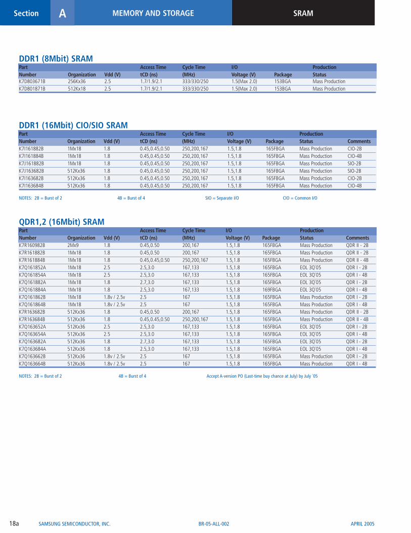
DDR1 (18Mbit) SRAMPart Access Time Cycle Time I/O Production Number Organization Vdd (V) tCD (ns) (MHz) Voltage (V) Package Status
K7D161874B 1Mx18 1.8~2.5 2.3 330/300 1.5 153BGA ES SamplesK7D163674B 512Kx36 1.8~2.5 2.3 330/300 1.5 153BGA ES Samples
ASection MEMORY AND STORAGE
18a
SRAM
SAMSUNG SEMICONDUCTOR, INC. APRIL 2005BR-05-ALL-002
DDR1 (8Mbit) SRAMPart Access Time Cycle Time I/O Production Number Organization Vdd (V) tCD (ns) (MHz) Voltage (V) Package StatusK7D803671B 256Kx36 2.5 1.7/1.9/2.1 333/330/250 1.5(Max 2.0) 153BGA Mass ProductionK7D801871B 512Kx18 2.5 1.7/1.9/2.1 333/330/250 1.5(Max 2.0) 153BGA Mass Production
DDR1 (16Mbit) CIO/SIO SRAM Part Access Time Cycle Time I/O Production Number Organization Vdd (V) tCD (ns) (MHz) Voltage (V) Package Status CommentsK7I161882B 1Mx18 1.8 0.45,0.45,0.50 250,200,167 1.5,1.8 165FBGA Mass Production CIO-2BK7I161884B 1Mx18 1.8 0.45,0.45,0.50 250,200,167 1.5,1.8 165FBGA Mass Production CIO-4BK7J161882B 1Mx18 1.8 0.45,0.45,0.50 250,200,167 1.5,1.8 165FBGA Mass Production SIO-2BK7J163682B 512Kx36 1.8 0.45,0.45,0.50 250,200,167 1.5,1.8 165FBGA Mass Production SIO-2BK7I163682B 512Kx36 1.8 0.45,0.45,0.50 250,200,167 1.5,1.8 165FBGA Mass Production CIO-2BK7I163684B 512Kx36 1.8 0.45,0.45,0.50 250,200,167 1.5,1.8 165FBGA Mass Production CIO-4B
NOTES: 2B = Burst of 2 4B = Burst of 4 SIO = Separate I/O CIO = Common I/O
QDR1,2 (16Mbit) SRAMPart Access Time Cycle Time I/O Production Number Organization Vdd (V) tCD (ns) (MHz) Voltage (V) Package Status CommentsK7R160982B 2Mx9 1.8 0.45,0.50 200,167 1.5,1.8 165FBGA Mass Production QDR II - 2BK7R161882B 1Mx18 1.8 0.45,0.50 200,167 1.5,1.8 165FBGA Mass Production QDR II - 2BK7R161884B 1Mx18 1.8 0.45,0.45,0.50 250,200,167 1.5,1.8 165FBGA Mass Production QDR II - 4BK7Q161852A 1Mx18 2.5 2.5,3.0 167,133 1.5,1.8 165FBGA EOL 3Q`05 QDR I - 2BK7Q161854A 1Mx18 2.5 2.5,3.0 167,133 1.5,1.8 165FBGA EOL 3Q`05 QDR I - 4BK7Q161882A 1Mx18 1.8 2.7,3.0 167,133 1.5,1.8 165FBGA EOL 3Q`05 QDR I - 2BK7Q161884A 1Mx18 1.8 2.5,3.0 167,133 1.5,1.8 169FBGA EOL 3Q`05 QDR I - 4BK7Q161862B 1Mx18 1.8v / 2.5v 2.5 167 1.5,1.8 165FBGA Mass Production QDR I - 2BK7Q161864B 1Mx18 1.8v / 2.5v 2.5 167 1.5,1.8 165FBGA Mass Production QDR I - 4BK7R163682B 512Kx36 1.8 0.45,0.50 200,167 1.5,1.8 165FBGA Mass Production QDR II - 2BK7R163684B 512Kx36 1.8 0.45,0.45,0.50 250,200,167 1.5,1.8 165FBGA Mass Production QDR II - 4BK7Q163652A 512Kx36 2.5 2.5,3.0 167,133 1.5,1.8 165FBGA EOL 3Q`05 QDR I - 2BK7Q163654A 512Kx36 2.5 2.5,3.0 167,133 1.5,1.8 165FBGA EOL 3Q`05 QDR I - 4BK7Q163682A 512Kx36 1.8 2.7,3.0 167,133 1.5,1.8 165FBGA EOL 3Q`05 QDR I - 2BK7Q163684A 512Kx36 1.8 2.5,3.0 167,133 1.5,1.8 165FBGA EOL 3Q`05 QDR I - 4BK7Q163662B 512Kx36 1.8v / 2.5v 2.5 167 1.5,1.8 165FBGA Mass Production QDR I - 2BK7Q163664B 512Kx36 1.8v / 2.5v 2.5 167 1.5,1.8 165FBGA Mass Production QDR I - 4B
NOTES: 2B = Burst of 2 4B = Burst of 4 Accept A-version PO (Last-time buy chance at July) by July `05

ASection MEMORY AND STORAGE
19a
SRAM
SAMSUNG SEMICONDUCTOR, INC.APRIL 2005 BR-05-ALL-002
DDR2 CIO/SIO (36Mbit) SRAMPart Access Time Cycle Time I/O Production Number Organization Vdd (V) tCD (ns) (MHz) Voltage (V) Package Status CommentsK7I321882M 2Mx18 1.8 0.45,0.45,0.50 250,200,167 1.5,1.8 165FBGA Mass Production CIO-2BK7I321884M 2Mx18 1.8 0.45,0.45,0.50 250,200,167 1.5,1.8 165FBGA Mass Production CIO-4BK7J321882M 2Mx18 1.8 0.45,0.45,0.50 250,200,167 1.5,1.8 165FBGA Mass Production SIO-2BK7I323682M 1Mx36 1.8 0.45,0.45,0.50 250,200,167 1.5,1.8 165FBGA Mass Production CIO-2BK7I323684M 1Mx36 1.8 0.45,0.45,0.50 250,200,167 1.5,1.8 165FBGA Mass Production CIO-4BK7J323682M 1Mx36 1.8 0.45,0.45,0.50 250,200,167 1.5,1.8 165FBGA Mass Production SIO-2B
NOTES: 2B = Burst of 2 4B = Burst of 4 SIO = Separate I/O CIO = Common I/O
QDR 2 (36Mbit) SRAMPart Access Time Cycle Time I/O Production Number Organization Vdd (V) tCD (ns) (MHz) Voltage (V) Package Status CommentsK7R320982M 4Mx9 1.8 0.45,0.50 200,167 1.5,1.8 165FBGA Mass Production QDR II-2BK7R321882M 2Mx18 1.8 0.45,0.50 200,167 1.5,1.8 165FBGA Mass Production QDR II-2BK7R321884M 2Mx18 1.8 0.45,0.45,0.50 250,200,167 1.5,1.8 165FBGA Mass Production QDR II-4BK7R323682M 1Mx36 1.8 0.45,0.50 200,167 1.5,1.8 165FBGA Mass Production QDR II-2BK7R323684M 1Mx36 1.8 0.45,0.45,0.50 250,200,167 1.5,1.8 165FBGA Mass Production QDR II-4B
NOTES: 2B = Burst of 2 4B = Burst of 4
QDR 2 (72Mbit) SRAMPart Access Time Cycle Time I/O Production Number Organization Vdd (V) tCD (ns) (MHz) Voltage (V) Package Status CommentsK7R640982M 8Mx9 1.8 0.45,0.45,0.50 250,200,167 1.5,1.8 165FBGA Mass Production Q2`05 QDR II-2BK7R641882M 4Mx18 1.8 0.45,0.45,0.50 250,200,167 1.5,1.8 165FBGA Mass Production Q2`05 QDR II-2BK7R641884M 4Mx18 1.8 0.45,0.45,0.45,0.50 300,250,200,167 1.5,1.8 165FBGA Mass Production Q2`05 QDR II-4BK7R643682M 2Mx36 1.8 0.45,0.45,0.50 250,200,167 1.5,1.8 165FBGA Mass Production Q2`05 QDR II-2BK7R643684M 2Mx36 1.8 0.45,0.45,0.45,0.50 300,250,200,167 1.5,1.8 165FBGA Mass Production Q2`05 QDR II-4B
NOTES: 2B = Burst of 2 4B = Burst of 4
DDR2 CIO/SIO (72Mbit) SRAMPart Access Time Cycle Time I/O Production Number Organization Vdd (V) tCD (ns) (MHz) Voltage (V) Package Status CommentsK7I641882M 4Mx18 1.8 0.45,0.45,0.45,0.50 300,250,200,167 1.5,1.8 165FBGA Mass Production Q2`05 CIO-2BK7I641884M 4Mx18 1.8 0.45,0.45,0.45,0.50 300,250,200,167 1.5,1.8 165FBGA Mass Production Q2`05 CIO-4BK7J641882M 4Mx18 1.8 0.45,0.45,0.45,0.50 300,250,200,167 1.5,1.8 165FBGA Mass Production Q2`05 SIO-2BK7I643682M 2Mx36 1.8 0.45,0.45,0.45,0.50 300,250,200,167 1.5,1.8 165FBGA Mass Production Q2`05 CIO-2BK7I643684M 2Mx36 1.8 0.45,0.45,0.45,0.50 300,250,200,167 1.5,1.8 165FBGA Mass Production Q2`05 CIO-4BK7J643682M 2Mx36 1.8 0.45,0.45,0.45,0.50 300,250,200,167 1.5,1.8 165FBGA Mass Production Q2`05 SIO-2B
NOTES: 2B = Burst of 2 4B = Burst of 4 SIO = Separate I/O CIO = Common I/O

ASection MEMORY AND STORAGE
20a
SRAM Ordering Information
SAMSUNG SEMICONDUCTOR, INC. APRIL 2005BR-05-ALL-002
ASYNCHRONOUS SRAM ORDERING INFORMATIONK 4 X X X X X X X X - X X X X X X X1 2 3 4 5 6 7 8 9 10 11 12 13 14 15 16 17 18
1. Memory (K)
2. Async SRAM: 6
3. Small Classification
E: Corner Vcc/Vss + Fast SRAMF: fCMOS Cell + LPSRAMH: High Speed(LPSRAM)X: High Voltage(LPSRAM)J: BICMOSL: Poly Load Cell + LPSRAMR: Center Vcc/Vss + Fast SRAMT: TFT Cell + LPSRAM
4~5. Density
06: 64K 08: 256K 09: 512K10: 1M 16: 16M 20: 2M30: 3M 32: 32M 40: 4M60: 6M 64: 64M 80: 8M
6~7. Organization
01: x1 04: x4 08: x816: x16 18: x18 24: x2432: x32
8. Vcc
5: 1.5V C: 5.0VQ: VDD 3.0V/VDDQ 1.8VR: 1.65V~2.2VS: 2.5V T: 2.7V~3.6V U: 3.0VV: 3.3V W: 2.2V~3.3V
9. Mode
1: CS Low Active2: CS1, CS2 - Dual Chip Select Signal3: Single Chip Select with /LB,/UB(tOE)4: Single Chip Select with /LB,/UB(tCS)5: Dual Chip Select with /LB,/UB(tOE)6: Dual Chip Select with /LB,/UB(tCS)7: I/Os Control with /BYTE8: CDMA Function9: Multiplexed AddressA: Mirror Chip Option
10. Generation
M: 1st GenerationA: 2nd Generation B: 3rd GenerationC: 4th Generation D: 5th GenerationE: 6th Generation F: 7th GenerationG: 8th Generation H: 9th Generation
11. " ----"
12. Package
A: TBGA(LF) B: SOP(LF)C: CHIP BIZ D: DIPE: TBGA F: FBGAG: SOP H: BGAJ: SOJ K: SOJ(LF)L: TSOP1-0813.4F(LF)P: TSOP1-0820F(LF)Q: TSOP2-400R(LF) R: TSOP-RT: TSOP U: TSOP2-400(LF)W: WAFER Z: UBGA
* Exception- 1MFSRAM B-ver32-SOJ-300 > S28-SOJ-300 > S- 512K/1M/2M/4M LPSRAM32-TSOP1-0813.4F > Y32-TSOP1-0813.4 > Y32-TSOP1-0813.4R > N- 4M LPSRAM32-TSOP2-400F > V32-TSOP2-400R > M
13. 1st Chip Speed
- COMMON (Temp,Power)A: Automotive,NormalB: Commercial,Low LowC: Commercial,NormalD: Extended,Low LowE: Extended,NormalF: Industrial,Low LowI: Industrial,NormalL: Commercial,LowM: Military,NormalN: Extended,LowP: Industrial,LowQ: Automotive,LowR: Industrial,Super LowT: Extended,Super LowU: Commercial,Ultra Super Low0: NONE,NONE- WAFER, CHIP BIZ Level Division0: NONE,NONE1: Hot DC sort2: Hot DC,selected AC sort3: Cold/Hot DC,selected AC sort
14~15. Speed (tAA)
- fCMOS Cell + LPSRAM & Poly Load Cell +LPSRAM & TFT Cell + LPSRAM10: 100ns12: 120ns15: 150ns25: 25ns(only fCMOS Cell)30: 300ns35: 35ns(except Poly Load Cell)45: 45ns(except fCMOS Cell)55: 55ns60: 60ns(only fCMOS Cell)70: 70ns85: 85ns90: 90ns(only fCMOS Cell)DS: Daisychain Sample- High Speed (LPSRAM)20: 20ns 25: 25ns- High Voltage (LPSRAM)55: 55ns 70: 70ns 85: 85ns- Corner Vcc/Vss + Fast SRAM10: 10ns 12: 12ns 13: 13ns15: 15ns 17: 17ns 20: 20ns25: 25ns 30: 30ns 35: 35ns45 :45ns- BICMOS & Center Vcc/Vss + Fast SRAM06: 6ns 08: 8ns 09: 9ns10: 10ns 12: 12ns 13: 13ns15: 15ns 17: 17ns 20: 20ns25: 25ns30: 30ns(only Center Vcc/Vss + Fast SRAM)35: 35ns(only Center Vcc/Vss + Fast SRAM)7A: 7.2ns(only BICMOS)8A: 8.6ns(only BICMOS)DS: Daisychain Sample- Async SRAM COMMON00: NONE(Containing Wafer, CHIP BIZ, Exception code)
16. Packing Type (16 digit)
- Common to all products, except of Mask ROM
- Divided into TAPE & REEL(In Mask ROM, divided into
TRAY, AMMO Packing Separately)
Type Packing Type New Marking
Component TAPE & REEL T
Other (Tray, Tube, Jar) 0 (Number)
Stack S
Component TRAY Y
(Mask ROM) AMMO PACKING A
Module MODULE TAPE & REEL P
MODULE Other Packing M

ASection MEMORY AND STORAGE
21aSAMSUNG SEMICONDUCTOR, INC.
SRAM Ordering Information
APRIL 2005 BR-05-ALL-002
SRAM ORDERING INFORMATIONK 4 X X X X X X X X - X X X X X X X1 2 3 4 5 6 7 8 9 10 11 12 13 14 15 16 17 18
1. Memory (K)
2. Sync SRAM: 7
3. Small Classification
A: Sync Pipelined Burst
B: Sync Burst
C: Custom Product
D: Double Data Rate
E: Double Data Rate 3-Clk Align
H: Double Data Rate I-Common I/O
I: Double Data Rate II-Common I/O
J: Double Data Rate-Separate I/O
L: Late Select
M: Sync Burst + NtRAM
N: Sync Pipelined Burst + NtRAM
P: Sync Pipe
Q: Quad Data Rate I
R: Quad Data Rate II
U: CSRAM
Z: DLW RAM
4~5. Density
10: 1M 16: 16M
20: 2M 32: 32M
40: 4M 44: 144M
64: 64M 72: 72M
80: 8M
6~7. Organization
08: x8 09: x9
18: x18 32: x32
36: x36 44: x144
72: x72
8~9. Vcc, Interface, Mode
00: 3.3V,LVTTL,2E1D WIDE01: 3.3V,LVTTL,2E2D WIDE08: 3.3V,LVTTL,2E2D Hi SPEED09: 3.3V,LVTTL,Hi SPEED11: 3.3V,HSTL,R-R12: 3.3V,HSTL,R-L14: 3.3V,HSTL,R-R Fixed ZQ22: 3.3V,LVTTL,R-R23: 3.3V,LVTTL,R-L25: 3.3V,LVTTL,SB-FT WIDE30: 1.8/2.5/3.3V,LVTTL,2E1D31: 1.8/2.5/3.3V,LVTTL,2E2D35: 1.8/2.5/3.3V,LVTTL,SB-FT44: 2.5V,LVTTL,2E1D
45: 2.5V,LVTTL,2E2D49: 2.5V,LVTTL,Hi SPEED52: 2.5V,1.5/1.8V,HSTL,Burst254: 2.5V,1.5/1.8V,HSTL,Burst462: 2.5V/1.8V,HSTL,Burst264: 2.5V/1.8V,HSTL,Burst466: 2.5V,HSTL,R-R70: 2.5V,HSTL,4-1-1-171: 2.5V,HSTL,3-1-1-173: 1.5V,1.8V,HSTL,All74: 1.8V,2.5V,HSTL,All80: 1.8V,LVCMOS,2E1D82: 1.8V,HSTL,Burst284: 1.8V,HSTL,Burst485: 1.8V,LVCMOS,2E2D,Hi SPEED88: 1.8V,HSTL,R-R91: 1.5V,HSTL,All95: 1.0V,HSTL,All
10. Generation
M: 1st GenerationA: 2nd GenerationB: 3rd GenerationC: 4th GenerationD: 5th GenerationZ: TEMPORARY CODE
11. “--”
12. Package
H: BGA,FCBGA,PBGA G: BGA,FCBGA,PBGA(LF)F: FBGA Q: (L)QFPC: CHIP BIZ W: WAFER
13. Temp, Power
- COMMON (Temp,Power)0: NONE,NONE (Containing of Error handling code)A: Automotive,Normal B: Commercial,Low LowC: Commercial,Normal E: Extended,Normal I: Industrial,Normal
- WAFER, CHIP BIZ Level Division0: NONE,NONE
1: Hot DC sort
2: Hot DC, selected AC sort
14~15. Speed
- Sync Burst,Sync Burst + NtRAM
& < Mode is R-L >(Clock Accesss Time)
10: 10ns(Sync Burst, Sync Burst + NtRAM)
38: 3.8ns 43: 4.3ns
48: 4.8ns
50: 5ns(Only Sync Pipe)
55: 5.5ns 60: 6ns
65: 6.5ns 67: 6.7ns
70: 7ns 75: 7.5ns
80: 8ns 85: 8.5ns
90: 9ns
- Other Small Classification (Clock Cycle Time)
10: 100MHz 11: 117MHz
13: 133MHz 14: 138MHz
15: 150MHz 16: 166MHz
17: 175MHz 18: 183MHz
19: 143MHz 20: 200MHz
21: 200MHz(2.0ns) 22: 225MHz
25: 250MHz
26: 250MHz(1.75ns) 27: 275MHz
30: 300MHz 33: 333MHz
35: 350MHz
36: 366MHz(t-CYCLE) 37: 375MHz40: 400MHz(t-CYCLE) 42: 425MHz
45: 450MHz
50: 500MHz(except Sync Pipe)
6A: 600MHz 6F: 650Mhz(Only CSRAM)
7F: 750MHz
16. Packing Type (16 digit)
- Common to all products, except of Mask ROM
- Divided into TAPE & REEL(In Mask ROM, divided into
TRAY, AMMO Packing Separately)
Type Packing Type New Marking
Component TAPE & REEL T
Other (Tray, Tube, Jar) 0 (Number)
Stack S
Component TRAY Y
(Mask ROM) AMMO PACKING A
Module MODULE TAPE & REEL P
MODULE Other Packing M

ASection MEMORY AND STORAGE
22a SAMSUNG SEMICONDUCTOR, INC.
MCPs
APRIL 2005BR-05-ALL-002
MCP: NAND/DRAM DENSITY PKG INFORMATION
ROM RAM Family Part No. Size Type256 128 ND256128 K5D5629CCM-F(D)095000 10.5x13x1.4 107FBGA
K5D5729CCM-F095000 10.5x13x1.4 107FBGAK5D5629ACB-D090(T)000 10.5x13x1.4 107FBGAK5D5729CCA-F(D)095000 10.5x13x1.4 127FBGA
256 256 ND256256 K5D5657ACM-F095T00 10.5x13x1.4 107FBGAK5D5657ACA-D090000 10.5x13x1.4 107FBGAK5D5657DCM-F095000 10.5x13x1.4 107FBGAK5D5757ACM-D090000 10.5x13x1.4 107FBGAK5D5658ACM-D090000 10.5x13x1.4 137FBGAK5D5658ECM-D075000 10.5x13x1.2 137FBGAK5E5658HCM-D060000 10.5x13x1.4 137FBGA
256 512 NDD256256256 KAL00B00CM-DG22000 10.5x13x1.4 107FBGAKAL00B00CA-DG22000 10.5x13x1.4 107FBGAKAL00Q00CM-DG55000 10.5x13x1.4 107FBGAKAL00B00EM-DG55000 10.5x13x1.4 107FBGA
512 256 NND565656 KAG00E007M-FGG2000 10.5x13x1.4 107FBGAKAG00J007M-F(D)GG2000 10.5x13x1.4 107FBGAKAG00H008M-FGG2000 10.5x13x1.4 107FBGAKAG00U00GM-FGG5000 10.5x13x1.4 107FBGAKAG00J00HM-FGG5000 10.5x13x1.4 137FBGA
ND512256 K5D1257ACM-D090000 10.5x13x1.4 107FBGAK5D1257DCM-D090000 10.5x13x1.4 107FBGAK5D1258ACM-D090T00 11.5x13x1.2 137FBGA
512 512 NNDD256256256256 KBE00M005M-D411000 10.5x13x1.4 137FBGAKBE00D004M-D411(3)000 10.5x13x1.4 137FBGAKBE00L007M-D415T00 10.5x13x1.4 137FBGA
NDD512256256 KAL00R00KM-DG55000 11.5x13x1.2 137FBGA1G 256 NND512512256 KAG00K007M-FGG2000 10.5x16x1.4 107FBGA
KAG00K007A-DGG5000 10.5x13x1.4 107FBGAKAG00L008M-FGG2000(3) 10.5x16x1.4 107FBGA
ND1G256 K5D1G58KCM-F(D)090000 14x14x1.1(POP) 119FBGA1G 512 NNDD512512256256 KBE00F003M-F(D)411000 10.5x16x1.4 107FBGA
KBE00F003A-D411000 10.5x13x1.4 107FBGAKBE00J006M-F411000 10.5x16x1.4 107FBGAKBE00F005M-F411000 10.5x16x1.4 137FBGAKBE00G005M-D411000 10.5x13x1.4 137FBGA
NDD1G256256 KAL00T00KM-DG55T00 11.5x13x1.2 137FBGAKAL00Z00LM-DA55000 11.5x13x1.4 137FBGA
ND1G512 K5D1G13ACM-D090000 14x14x1.15(POP) 152FBGA2G 512 NNDD1G1G256256 KBE00S003M-D411000 12x14x1.4 107FBGA
KBE00S005M-D411000 137FBGAKBE00H005M-F411000 11.5x13x1.4 137FBGA
NOTES: N=NAND D=DRAM See sales rep for product details

23a
ASection MEMORY AND STORAGEMCPs
SAMSUNG SEMICONDUCTOR, INC.APRIL 2005 BR-05-ALL-002
MCP: NOR/SRAM AND NOR/UtRAM DENSITY NOR PKG INFORMATION
ROM RAM Family Org Part No. Size Type32 4 RS3204 x8/x16 K5A3240YTC-T755000 8_11_1.2 69TBGA
K5A3240YBC-T755000K5A3240CTM-F755000 8_11_1.2 69FBGAK5A3240CBM-F755000
32 8 RS3208 x8/x16 K5A3280YTC-T755000 8_11_1.2 69TBGAK5A3280YBC-T755000K5A3281CTM-F(D)755000 8_11_1.2 69FBGAK5A3281CBM-F(D)755000
64 16 RU6416 x16 K5J6316CTM-F770000 8_11.6_1.4 69FBGAK5J6316CBM-F770000
128 16 RRU646416 x8x16 KAD060J00M-FLLL000 8_11.6_1.4 69FBGAKAD070J00M-FLLL000
128 32 RRU646432 x8x16 KAD060300B-TLLL000 8_11.6_1.4 69TBGAKAD070300B-TLLL000KAD060300C-FLLL000 8_11.6_1.4 69FBGAKAD070300C-FLLL000
256 128 RRU128128128 x16 KAD190F00M-DUUUT00 8x12x1.4 115FBGARU256128 x16 K5L5628JTM-DH18T00 8x12x1.4 115FBGA
K5L5628JBM-DH18000256 192 RUU25612864 x16 KAH170K00M-DUUUT00 8x12x1.4 115FBGA
KAH220K00M-DUUUT00
NOTES: N=NAND R=NOR S=SRAM U=UtRAM See sales rep for product details
MCP: OneNAND™/DRAM DENSITY PKG INFORMATION
ROM RAM Family Part No. Size Type1G 512 ODD1G256256 KAT00W00EM-DU55000 11.5x13x1.4 167FBGA
NOTES: O=OneNAND D=DRAM See sales rep for product details
MCP: NOR/DRAM DENSITY PKG INFORMATION
ROM RAM Family Part No. Size Type32 128 RD32128 K5H3228CTM-D81H000 10x13x0.8 120FBGA32 256 RDD32128128 KAN15000DA-DL22000 10.5x13x1.4 167FBGA64 256 RD64256 K5H6358ETM-D775000 10x11x0.8(0.65) 145FBGA256 128 RD256128 K5K5629ATA-DF90000 9x11x1.4 103FBGA512 128 RRD256256128 KAS230009A-D445000 9x11x1.4 103FBGA
NOTES: R=NOR D=DRAM See sales rep for product details

ASection MEMORY AND STORAGE MCPs
24a SAMSUNG SEMICONDUCTOR, INC. APRIL 2005BR-05-ALL-002
MCP: NOR/OneNAND/UtRAM DENSITY PKG INFORMATION
ROM RAM Family Part No. Size Type192 32 RNU6412832 KAB02D100M-TLGP000 8_12_1.4 80TBGA
KAB01D100M-TLGP000KAB02D100A-FLGL000 8_12_1.4 80FBGAKAB01D100A-FLGL000
256 32 RRNU646412832 KBB06A300M-T402000 8_12_1.4 80TBGAKBB05A300M-T402000KBB06A300A-D402000 8_12_1.4 80FBGAKBB05A300A-D402000
256 64 RRNU646412864 KBB06A500M-T402000 8_13_1.4 80TBGAKBB05A500M-T402000KBB06A500A-D402000 8_13_1.4 80FBGAKBB05A500A-D402000
384 64 RRNU646425664 KBB06B400M-F(D)402000 8_13_1.4 80FBGAKBB05B400M-F(D)402000KBB06B500A-D402000 8_13_1.4 80FBGAKBB05B500A-D402000
384 128 ROU256128128 KAP17YG00M-DUUU000 8_13_1.4 80FBGAKAP22YG00M-DUUU000
512 128 ROU256256128 KAP20VH00A-DL8L000 8_13_1.4 80FBGAKAP21VH00A-DL8L000KAP17VG00M-DUUU000KAP22VG00M-DUUU000
768 128 ROU256512128 KAP17SG00A-D4U4000 10.5x14x1.4 167FBGA768 256 ROUU256512128128 KBH10EA00A-D414000 10.5x14x1.4 167FBGA
KBH10ED00A-D4140001280 128 ROOU256512512128 KBJ16KC00A-D418000 10.5x14x1.4 167 FBGA
KBJ17KC00A-D418000KBJ10KB00A-D416000KBJ11KB00A-D416000
1280 256 ROUU2561G128128 KBH16PE00M-D421000(1C/S) 10.5x14x1.4 167 FBGAKBH17PE00M-D4210(T)00(1C/S)KBH10PD00M-D414000(1C/S)
NOTES: R=NOR O=OneNAND N=NAND U=UtRAM See sales rep for product details

ASection MEMORY AND STORAGEOptical Storage
25aSAMSUNG SEMICONDUCTOR, INC.BR-05-ALL-002
COMBO DRIVETS-H492A 52X 32X 52X CD-RW + 16X DVD-ROMRecording Drive Loading Average Dimensions Buffer Drive SupportedCapacity Type Interface Type Access Time (WxHxDmm) Memory Mounting Disc
CD-RW Disc 700/650MB Internal EIDE/ATAPI Motorized CD-RW, DVD: 130ms 148.2 x 42 x 184 2MB Horizontal/Vertical DVD/RAM. DVD±R/RW(Type 80/74) Type Tray Type CD: 110ms DVD-ROM, DVD-Video,CDR Disc 800/700/650MB CD-R, CD-RW, CD-DA, CD-ROM,
CD ROM/XA, VideoCD, CD-I,PhotoCD, CD-EXTRA,CD TEXT
CR-RW DRIVETS-H292A 52X Write / 32X ReWrite / 52X Read
Recording Drive Loading Average Dimensions Buffer Drive SupportedCapacity Type Interface Type Access Time (WxHxDmm) Memory Mounting Disc
CD-RW Disc 700/650MB Internal EIDE/ATAPI Motorized (SW-252F) 100ms 148.2 x 42 x 184 2MB Horizontal/Vertical CD-R/CD-RW, CD-DA, CD-ROM,(Type 80/74) Type Tray Type CD-ROM/XA, VideoCD,CDR Disc 800/700/650MB CD-I, PhotoCD, CD-EXTRA,(Type 90/80/74) CD-TEXT
CD-ROM DRIVESH-152A 52X Multi-Read CD-ROM Drive
Drive Disc Loading Average Dimensions Buffer Drive SupportedType Interface Diameter Type Access Time (WxHxDmm) Memory Mounting Disc
Internal EIDE/ATAPI 80mm / 120mm Motorized 80ms (SC-152) 148.2 x 42 x 184 128KB Horizontal/Vertical CD-R/RW, CD-DA, CD-ROM,Type Tray Type CD-ROM/XA, VideoCD,
CD-I, Photo CD, CD-EXTRA, CD-TEXT
DVD-ROM DRIVETS-H352A 16X Multi-Read DVD-ROM Drive
Drive Loading Average Dimensions Buffer Drive SupportedType Interface Type Access Time (WxHxDmm) Memory Mounting Disc
Internal EIDE/ATAPI Motorized DVD 90ms 148.2 x 42 x 184 512KB Horizontal/Vertical DVD-RAM, DVD-R, DVD-RW, DVD-ROM,Type Tray Type CD 90ms DVD-Video, CD-R/RW, CD-DA, CD-ROM,
CD-ROM/XA, Video-CD, CD-I, Photo CD,CD-EXTRA, CD-TEXT
DVD-MULTI RECORDERTS-H552U DVD±R/RW + CD-R/CD-RW
Drive Average Dimensions Buffer SupportedType Interface Seek Time (WxHxDmm) Memory Disc
Internal Type EIDE/ATAPI CD-ROM 130ms 148 x 42 x 200 2MB DVD-ROM, DVD±R/RW, DVD-Video,
DVD-S 130ms CD-R/RW, CD-DA, CD-ROM, CD-ROM-XA,DVD-R/DVD-RW 150ms Video-CD, CD-I, Photo CD, CD-EXTRA, CD-TEXTDVD-RAM 170ms
APRIL 2005

ASection MEMORY AND STORAGE Hard Disk Drives
26a SAMSUNG SEMICONDUCTOR, INC. APRIL 2005BR-05-ALL-002
HARD DISK DRIVES (HDD)
Capacity RPMs Model # of Heads # of Disks Interface Buffer Size Seek Time MTBF
SpinPoint V Series V80 Series 80GB 5400 rpm SV0802N 2 1 ATA-133 2MB / 8MB 8.9ms 500K hrs120GB 5400 rpm SV1203N 3 2 ATA-133 2MB / 8MB 8.9ms 500K hrs160GB 5400 rpm SV1604N 4 2 ATA-133 2MB / 8MB 8.9ms 500K hrs
SpinPoint P Series P80 Series 80GB 7200 rpm SP0802N 2 1 ATA-133 2MB / 8MB 8.9ms 500K hrs120GB 7200 rpm SP1203N 3 2 ATA-133 2MB / 8MB 8.9ms 500K hrs160GB 7200 rpm SP1604N 4 2 ATA-133 2MB / 8MB 8.9ms 500K hrs
P40 Series 40GB 7200 rpm SP0411N 1 1 ATA-133 2MB 10ms 500K hrsP80 Series SATA 80GB 7200 rpm SP0812C 2 1 S-ATA 8MB 10ms 500K hrs
120GB 7200 rpm SP1213C 3 2 S-ATA 8MB 10ms 500K hrs160GB 7200 rpm SP1614C 4 2 S-ATA 8MB 10ms 500K hrs
P40 Series SATA 40GB 7200 rpm SP0411C 1 1 S-ATA 2MB 10ms 500K hrsP120 Series 200GB 7200 rpm SP2014N 4 2 ATA-133 8MB 8.9ms 500K hrs
250GB 7200 rpm SP2514N 4 2 ATA-133 8MB 8.9ms 500K hrsP120 Series SATA 200GB 7200 rpm SP2004C 4 2 S-ATA 8MB 8.9ms 600K hrs
250GB 7200 rpm SP2504C 4 2 S-ATA 8MB 8.9ms 600K hrs
2.5“ HARD DISK DRIVES (HDD)
Capacity Rotational Speed P/N # of Head # of Disk Interface Buffer Size
SpinPoint M Series M40 Series 30GB 5400 rpm MP0302H 1 1 ATA-6 8MB
40GB 5400 rpm MP0402H 2 1 ATA-6 8MB
60GB 5400 rpm MP0603H 3 2 ATA-6 8MB
80GB 5400 rpm MP0804H 4 2 ATA-6 8MB
M40 Series SATA 40GB 5400 rpm HM040HI 2 1 S-ATA 8MB
60GB 5400 rpm HM060HI 3 2 S-ATA 8MB
80GB 5400 rpm HM080HI 4 2 S-ATA 8MB

Samsung offers the industry’s broadest memory
portfolio and has maintained its leadership in
memory technology for 12 straight years. Its
DRAM, SRAM and Flash product lines are
found in computers – from notebooks to
powerful servers – and in a wide range of
handheld devices such as smartphones.
Samsung also delivers high-value storage
products. These include: optical disk drives
used in business storage devices and consumer
electronics; and hard disk drives for mobile
computers and consumer devices like cellphones.
For more information, visit our website: www.usa.samsungsemi.com
Disclaimer: The information in this publication has been carefully checked and is believed to be accurate at the timeof publication. Samsung assumes no responsibility, however, for possible errors or omissions, or for any consequencesresulting from the use of the information contained herein. Samsung reserves the right to make changes in its prod-ucts or product specifications with the intent to improve function or design at any time and without notice and is notrequired to update this documentation to reflect such changes. This publication does not convey to a purchaser ofsemiconductor devices described herein any license under the patent rights of Samsung or others. Samsung makes nowarranty, representation, or guarantee regarding the suitability of its products for any particular purpose, nor doesSamsung assume any liability arising out of the application or use of any product or circuit and specifically disclaimsany and all liability, including without limitation any consequential or incidental damages.

www.usa.samsungsemi.comCopyright 2005. Samsung and Samsung Semiconductor, Inc. are registered trademarks of Samsung Electronics, Co., Ltd. All other names and brands may be claimed as the property ofothers. The appearance of all products, dates, figures, diagrams and tables are subject to change at any time, without notice.
BR-05-ALL-002 Printed 4/05