Memory, Latches, & Registers - University of North ... · from physics that we can “store” a...
25
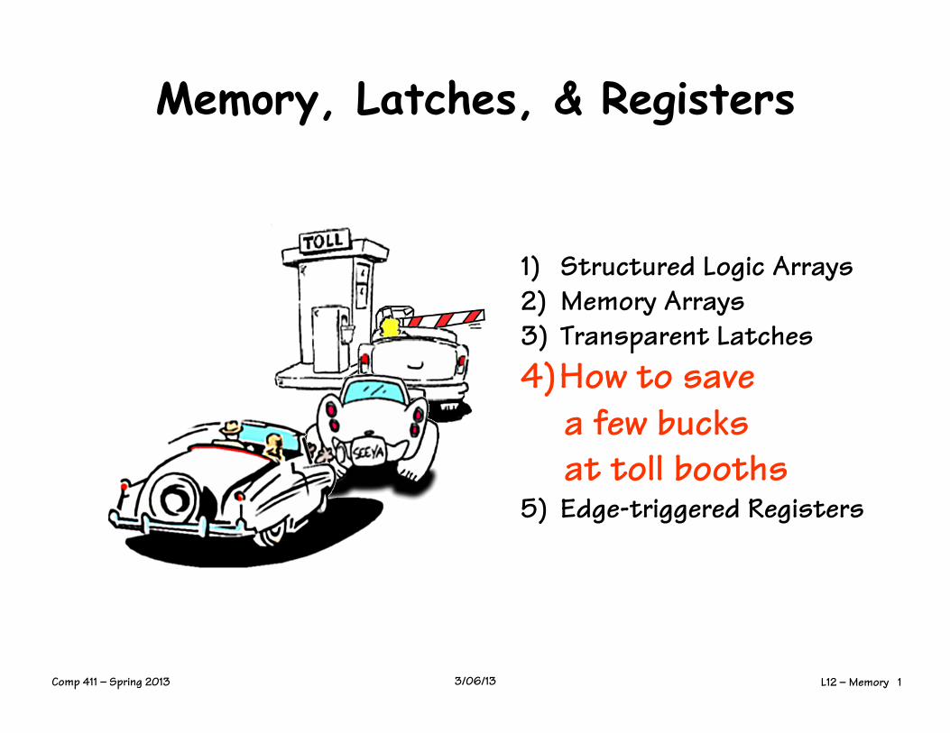
L12 – Memory 1 Comp 411 – Spring 2013 3/06/13 Memory, Latches, & Registers 1) Structured Logic Arrays 2) Memory Arrays 3) Transparent Latches 4)How to save a few bucks at toll booths 5) Edge-triggered Registers
Transcript of Memory, Latches, & Registers - University of North ... · from physics that we can “store” a...
L12 – Memory 1 Comp 411 – Spring 2013 3/06/13
Memory, Latches, & Registers
1) Structured Logic Arrays 2) Memory Arrays 3) Transparent Latches 4) How to save
a few bucks at toll booths
5) Edge-triggered Registers

L12 – Memory 2 Comp 411 – Spring 2013 3/06/13
General Table Lookup Synthesis
MUX Logic
A B
Fn(A,B)
Generalizing: Remember from a few lectures ago that, in theory, we can build any 1-output combinational logic block with multiplexers.
For an N-input function we need a _____ input multiplexer.
BIG Multiplexers? How about 10-input function? 20-input?
2N

L12 – Memory 3 Comp 411 – Spring 2013 3/06/13
A Mux’s Guts
Hmmm, by sharing the decoder part of the logic MUXs could be adapted to make lookup tables with any number of outputs
I 0 0
I 0 1
I 1 0
I 1 1
A B A B A B A B
Y
Decoder Selector Multiplexers can be partitioned into two sections.
A DECODER that identifies the
desired input,and
a SELECTOR that enables that input onto the output.
A decoder generates all possible
product terms for a set of inputs
0
1
2
3

L12 – Memory 4 Comp 411 – Spring 2013 3/06/13
A New Combinational Device
k
D1 D2
DN
DECODER:
k SELECT inputs,
N = 2k DATA OUTPUTs.
Selected Dj HIGH; all others LOW.
NOW, we are well on our way to building a general purpose table-lookup device.
We can build a 2-dimensional ARRAY of decoders and selectors as follows ...
Have I mentioned that HIGH
is a synonym for ‘1’ and
LOW means the same
as ‘0’

L12 – Memory 5 Comp 411 – Spring 2013 3/06/13
Shared Decoding Logic
0 2 3 4 5 6 7 1
A B Cin
S
Cout
There’s an extra level
of inversion that isn’t necessary
in the logic. However,
it reduces the capacitive load on the
module driving this one.
These are just “DeMorgan”ized
NOR gates
Made from PREWIRED connections , and CONFIGURABLE connections that can be either connected or not connected
We can build a general purpose “table-lookup” device called a Read-Only Memory (ROM), from which we can implement any truth table and, thus, any combinational device
Decoder
Configurable Selector
This ROM stores 16 bits in 8 words of 2 bits.

L12 – Memory 6 Comp 411 – Spring 2013 3/06/13
ROM Implementation Details
Hardwired “AND” logic Programmable “OR” logic
Advantages: - Very regular design (can be entirely automated)
Problems: - Active Pull-ups (Static Power) - Long metal runs (Large Caps) - Slow
A
B
Cin
S Cout
JARGON: Inputs to
a ROM are called
ADDRESSES. The decoder’s outputs are
called WORD LINES,
and the outputs lines
of the selector are
called BIT LINES.
Tiny PFETs with gates tied to ground = resistor pullup that makes wire “1” unless one of the NFET pulldowns is on.
Decoder Values: 0 1 2 3 4 5 6 7
A “word”-line.
A “bit”-line
These transistors are function “dependent”
These transistors implement a
decoder, and are
independent
of function.

L12 – Memory 7 Comp 411 – Spring 2013 3/06/13
Logic According to ROMs ROMs ignore the structure of combinational functions ...
• Size, layout, and design are independent of function • Any Truth table can be “programmed” by minor reconfiguration:
- Metal layer (masked ROMs) - Fuses (Field-programmable PROMs) - Charge on floating gates (EPROMs) ... etc.
Model: LOOK UP value of function in truth table... Inputs: “ADDRESS” of a T.T. entry ROM SIZE = # TT entries...
... for an N-input boolean function, size = __________ 2N x #outputs

L12 – Memory 8 Comp 411 – Spring 2013 3/06/13
Example: 7-sided Die What nature can’t provide… electronics can
(and with the same number of LEDs!).
We want to construct a die with the following sides:
An array of LEDs, labeled as follows, can be used to display the outcome of the die:
T V X
U
Y Z
W

L12 – Memory 9 Comp 411 – Spring 2013 3/06/13
ROM-Based Design
Once we’ve written out the truth table we’ve basically finished the design
Possible optimizations: - Eliminate redundant
outputs - Addressing tricks
Truth Table for a 7-sided Die
T
V X
U
Y Z
W

L12 – Memory 10 Comp 411 – Spring 2013 3/06/13
A Simple ROM implementation
A
B
C
T/Z U/Y V/X W
That was Easy! ROMs are even more flexible than MUXes, because you can design the H/W first, and figure out the logic later!
This is the essence of programability: “LATE-BINDING” logic specification.
T
V X
U
Y Z
W
Decoder Values: 0 1 2 3 4 5 6 7

L12 – Memory 11 Comp 411 – Spring 2013 3/06/13
“Programmable” Look-up Tables Remember, EVERY combinational circuit can be expressed as a lookup table. As a result a ROM is a universal logic device. Unfortunately, the ROMs we’ve built thus far are “HARDWIRED”. That is, the function that they compute is encoded by the pull-down transistors that are built into the OR-plane of the ROM. What we’d really like is a combinational gate that could be reconfigured dynamically. For this we’ll need some form of storage.
WORD line
BIT line
How to “store” a
“bit”? The function of a
ROM is determined by the
presence of a transistor at the intersection of a WORD line from the AND array with a BIT line
going to the OR array

L12 – Memory 12 Comp 411 – Spring 2013 3/06/13
Analog Storage: Using Capacitors
We’ve chosen to encode information using voltages and we know from physics that we can “store” a voltage as “charge” on a capacitor:
bit line
N-channel FET serves
as an access switch
VREF
Pros: compact! Cons: it leaks! ⇒ refresh complex interface reading a bit, destroys it (you have to rewrite the value after each read)
it’s NOT a digital circuit
To write: Drive bit line, turn on access fet, force storage cap to new voltage To read: precharge bit line, turn on access fet, detect (small) change in bit line voltage
word line
This storage circuit is the basis for commodity DRAMs

L12 – Memory 13 Comp 411 – Spring 2013 3/06/13
Dynamic Memory
TiN top electrode
(VREF)
Ta2O5 dielectric
poly word line
access FET

L12 – Memory 14 Comp 411 – Spring 2013 3/06/13
Y
S
B
A “Digital” Storage Element
It’s also easy to build a settable DIGITAL storage element (called a latch) using a MUX and FEEDBACK:
0
1
G
0 0 1 1
D
-- -- 0 1
QIN
0 1 -- --
QOUT
0 1 0 1
Q follows D
Q stable
“state” signal appears as both input and output
A
D
G
Q
Here’s a feedback path, so it’s no longer a combinational circuit.

L12 – Memory 15 Comp 411 – Spring 2013 3/06/13
Looking Under the Covers Let’s take a quick look at the equivalent circuit for our MUX
when the gate is LOW (the feedback path is active)
D G=0
Q Q
G=0
D
0
1
1
1 Q
This storage circuit is the basis for commodity SRAMs
Advantages: 1) Maintains remembered state for as long as power is applied. 2) State is DIGITAL Disadvantage: 1) Requires more transistors

L12 – Memory 16 Comp 411 – Spring 2013 3/06/13
Why Does Feedback = Storage?
BIG IDEA: use positive feedback to maintain storage indefinitely. Our logic gates are built to restore marginal signal levels, so noise shouldn’t be a problem!
VIN VOUT
Result: a bistable storage element
Feedback constraint: VIN = VOUT
VTC for inverter pair
VIN
VOUT Three solutions: two end-points are stable middle point is unstable
Not affected by noise
We’ll get back to this!

L12 – Memory 17 Comp 411 – Spring 2013 3/06/13
Static D Latch
G
D Q
D
G
Q stable
Q follows D
Positive latch
Q
“static” means latch will hold data (i.e., value of Q) while G is inactive, however long that may be.
G
D Q
Negative latch
Q
G
D
1
0
What is the difference?

L12 – Memory 18 Comp 411 – Spring 2013 3/06/13
A DYNAMIC Discipline Design of sequential circuits MUST guarantee that inputs to sequential devices are valid and stable during periods when they may influence state changes. This is assured with additional timing specifications.
G
D
>tPULSE
tPULSE: minimum pulse width guarantee G is active for long enough for latch to capture data
>tSETUP
tSETUP: setup time guarantee that D value has propagated through feedback path before latch closes
>tHOLD
tHOLD: hold time guarantee latch is closed and Q is stable before allowing D to change

L12 – Memory 19 Comp 411 – Spring 2013 3/06/13
Does this work?
ROM 64x4
unlock
Next state Current state
“1” button
“0” button
“start” button
3 3
D Q
G Hmm. Hard to get pulse width exactly right!

L12 – Memory 20 Comp 411 – Spring 2013 3/06/13
Flakey Control Systems
Here’s a strategy for saving 2 bucks the next time you find yourself at a toll booth!

L12 – Memory 21 Comp 411 – Spring 2013 3/06/13
G
D Q
G
D Q
Edge-triggered Flip Flop logical “escapement”
D Q D
CLK
Q D
CLK
Q master slave
Observations: only one latch “transparent” at any time:
master closed when slave is open (CLK is high) slave closed when master is open (CLK is low)
→ no combinational path through flip flop
Q only changes shortly after 0 →1 transition of CLK, so flip flop appears to be “triggered” by rising edge of CLK
Transitions mark instants, not
intervals

L12 – Memory 22 Comp 411 – Spring 2013 3/06/13
Flip Flop Waveforms
G
D Q
G
D Q D Q D
CLK
Q D
CLK
Q master slave
D
CLK
Q
master closed slave open
slave closed master open

L12 – Memory 23 Comp 411 – Spring 2013 3/06/13
Two Issues
G
D Q
G
D Q D Q master slave
CLK
• Must allow time for the input’s value to propagate to the Master’s output while CLK is LOW.
• This is called “SET-UP” time
• Must keep the input stable, just after CLK transitions to HIGH. This is insurance in case the SLAVE’s gate opens just before the MASTER’s gate closes.
• This is called “HOLD-TIME”
• Can be zero (or even negative!)
• Assuring “set-up” and “hold” times is what limits a computer’s performance

L12 – Memory 24 Comp 411 – Spring 2013 3/06/13
Flip-Flop Timing Specs
CLK
D
Q D Q D
CLK
Q <tPD
tPD: maximum propagation delay, CLK →Q
>tSETUP
tSETUP: setup time guarantee that D has propagated through feedback path before master closes
>tHOLD
tHOLD: hold time guarantee master is closed and data is stable before allowing D to change

L12 – Memory 25 Comp 411 – Spring 2013 3/06/13
Summary • Regular Arrays can be used to implement arbitrary logic functions
• ROMs decode every input combination (fixed-AND array) and compute the output for it (customized-OR array) • PLAs decode an minimal set of input combinations (both AND and OR arrays customized)
• Memories • ROMs are HARDWIRED memories • RAMs include storage elements at each WORD-line and BIT-line intersection • dynamic memory: compact, only reliable short-term • static memory: controlled use of positive feedback
• Level-sensitive D-latches for static storage • Dynamic discipline (setup and hold times)