
Meeting Hudson Mohawk Chapter of the AVS Sept.€¦ · Fall Meeting Hudson Mohawk Chapter of the...
18
Fall Meeting Hudson Mohawk Chapter of the AVS Sept. 28, 2015 1 Union College 807 Union Street Schenectady, NY 12308 Wold Center Atrium & Olin Center Center (Rm 106) AGENDA 4:00 PM Reception and Refreshments (Wold Center Atrium) 4:30 PM Welcome, Kim Michelle Lewis, Rensselaer Polytechnic Institute National AVS Update, Vincent Smentkowski, GE (Olin Center 106) 4:40 PM Oral Presentations (Olin Center 106) 6:30 PM Poster Presentations and Dinner (Wold Center Atrium) 8:00 PM Best Poster and Oral Presentation Awards (Wold Center Atrium) 8:05 PM Adjourn (Brief meeting of Chapter Board Members) (Wold Center Atrium)
-
Upload
nguyendieu -
Category
Documents
-
view
216 -
download
0
Transcript of Meeting Hudson Mohawk Chapter of the AVS Sept.€¦ · Fall Meeting Hudson Mohawk Chapter of the...

Fall Meeting Hudson Mohawk Chapter of the AVS Sept. 28, 2015
1
Union College 807 Union Street
Schenectady, NY 12308 Wold Center Atrium & Olin Center Center (Rm 106)
AGENDA
4:00 PM Reception and Refreshments (Wold Center Atrium) 4:30 PM Welcome, Kim Michelle Lewis, Rensselaer Polytechnic Institute
National AVS Update, Vincent Smentkowski, GE (Olin Center 106)
4:40 PM Oral Presentations (Olin Center 106) 6:30 PM Poster Presentations and Dinner (Wold Center Atrium) 8:00 PM Best Poster and Oral Presentation Awards (Wold Center Atrium) 8:05 PM Adjourn (Brief meeting of Chapter Board Members) (Wold Center
Atrium)

Fall Meeting Hudson Mohawk Chapter of the AVS Sept. 28, 2015
2
ORAL PRESENTATIONS AN STM INVESTIGATION OF THE REACTION OF HYDROGEN WITH CHEMISORBED OXYGEN ON Cu(110) Qianqian Liu and Guangwen Zhou Department of Mechanical Engineering & Multidisciplinary Program in Materials Science and
Engineering, State University of New York, Binghamton, NY 13902
EFFECTS OF POST‐DEPOSITION HYBRID ANNEAL ON THE OPTICAL, PHOTOLUMINESCENCE, AND STRUCTURAL PROPERTIES OF SiCxOy MATERIALS Brian Ford, Natasha Tabassum, Mounika Kotha, Lukas Kiehl, Maik Katko, Vasileios Nikas, Alain E. Kaloyeros and Spyros Gallis Colleges of Nanoscale Sciences and Engineering, State University of New York Polytechnic Institute,
Albany, New York 12203
METROLOGY FOR ATOMIC LAYER DEPOSITED HIGHER‐K METAL OXIDE SEMICONDUCTOR BASED DEVICES Sonal Dey and Alain Diebold
Colleges of Nanoscale Science & Engineering, SUNY Polytechnic Institute, 257 Fuller Rd., Albany, NY
12203
WILL ZINC OXIDE SERVE AS AN ELECTRONIC MATERIAL FOR FUTURE HIGH‐POWER AND HIGH‐FREQUENCY ELECTRON DEVICE APPLICATIONS? Poppy Siddiqua1, Walid A. Hadi1, Stephen K. O’Leary1, and Michael S. Shur2 1School of Engineering, The University of British Columbia, Kelowna, British Columbia V1V 1V7 2Department of Electrical, Computer, and Systems Engineering, Rensselaer Polytechnic Institute, Troy, New York 12180
STRONG METAL SUPPORT INTERACTION OF Pt ON TiO2 GROWN BY ATOMIC LAYER DEPOSITION FOR FUEL CELL APPLICATIONS R. Paul Hansen, Richard Phillips, Eric Eisenbraun, and Carl Ventrice, Jr.
Colleges of Nanoscale Science and Engineering, SUNY Polytechnic Institute, Albany, NY

Fall Meeting Hudson Mohawk Chapter of the AVS Sept. 28, 2015
3
ORAL PRESENTATION ABSTRACTS
AN STM INVESTIGATION OF THE REACTION OF HYDROGEN WITH CHEMISORBED OXYGEN ON Cu(110)
Qianqian Liu, Guangwen Zhou
Department of Mechanical Engineering & Multidisciplinary Program in Materials Science and
Engineering, State University of New York, Binghamton, NY 13902
Email: [email protected] The interaction of hydrogen with oxygen adsorbed on metal surface is widely studied because of its
relevance to a wide range of technological processes such as heterogeneous catalysis, but the atomic
processes leading to the transition of different oxygen chemisorbed phases are still poorly understood.
In our work, Scanning Tunneling Microscopy (STM) is employed to study the evolution of oxygen
chemisorption induced surface reconstruction of Cu(110) during the reaction of chemisorbed oxygen
and hydrogen . The reduction is performed at 150 °C with hydrogen pressure varying from 1 × 10‐8 Torr
to 5 × 10‐5 Torr on the chemisorbed‐oxygen covered Cu(110) surface. Cu(110)‐c(6×2) phase transits to
the (2×1) phase along the step edges and then the (2×1) phase grows larger and finally covers the entire
surface with higher hydrogen exposure. We show that the (6×2) → (2×1) transi on occurs via the H2
induced loss of chemisorbed oxygen in the (6x2) phase, resulting on releases extra Cu atoms diffusing
to the step edges and terraces. The STM observation of the atomic processes of the H2‐induced (6×2) →
(2×1) transition will be described in detail.

Fall Meeting Hudson Mohawk Chapter of the AVS Sept. 28, 2015
4
EFFECTS OF POST‐DEPOSITION HYBRID ANNEAL ON THE OPTICAL, PHOTOLUMINESCENCE, AND STRUCTURAL PROPERTIES OF SiCxOy MATERIALS
Brian Ford, Natasha Tabassum, Mounika Kotha, Lukas Kiehl, Maik Katko, Vasileios Nikas, Alain E.
Kaloyeros and Spyros Gallis
Colleges of Nanoscale Sciences and Engineering, State University of New York Polytechnic Institute, Albany, New York 12203, USA
Email: [email protected]
Silicon‐oxycarbide (SiCxOy) materials have been the focus of studies due to their potential use in a plethora of technological applications such as white light emitting materials,1,2 hydrogen storage materials,3 gas sensors,4 and even in biomedical devices.5 Prior work by the investigators has been dedicated to the development of a thermal CVD strategy for the growth of SiCxOy thin films for light emission applications. It is demonstrated that the as‐deposited SiCxOy thin films follow closely the pure silicon‐oxycarbide stoichiometry [SiCxO2(1‐x), (0<x<1)] and exhibit strong white light emission, originating from the recombination of photo‐generated carriers between the energy bands and at their tail states, associated with the Si‐O‐C/Si‐C bonding configuration.1,6 Herein we present results from a systematic study of the effects of single‐ and multi‐step (hybrid) post‐deposition passivation treatments on the structural, optical, and photoluminescence (PL) characteristics of two sets of SiCxOy films, namely carbon‐rich (SiC0.5O1.3) and oxygen‐rich (SiC0.3O1.6). The effects of different ramifications of oxygen and forming gas (FG) (H2 5 at.%, N2 95 at.%) thermal passivation treatments on the structural and optical properties of the resulting samples were investigated using Fourier transform infrared spectroscopy (FTIR), spectroscopic ultraviolet‐visible ellipsometry (UV‐VIS‐SE), and x‐ray photoelectron spectroscopy (XPS) measurements. A two‐step hybrid passivation process, comprising of an oxygen (500oC) then a forming gas (700oC) treatment, resulted in an approximately seven‐fold enhancement of the white luminescence in the visible/ultraviolet range (1.5 ‐ 4.0 eV). Time resolved PL and FTIR analysis showed that the luminescence enhancement is related to the decrease of the non‐radiative recombination paths through carbonyl sites. To that end, an inverse correlation between the carbonyl groups and the PL intensity is reported. In addition to the PL enhancement due to the engineering of the quenching centers in SiCxOy, a complementary PL three‐fold enhancement by sub‐100nm thermal CVD‐grown SiCxOy nanowire (NW) arrays fabricated by e‐beam lithography and reactive‐ion‐etching will also be reported. 1 S. Gallis, V. Nikas, H. Suhag, M. Huang, and A.E. Kaloyeros, Appl. Phys. Lett. 97, 081905 (2010). 2 A. V Vasin, Functional Nanomaterials and Devices for Electronics, Sensors and Energy Harvesting (Springer International Publishing, Cham, 2014). 3 Q.D. Nghiem, S.J. Cho, and D.‐P. Kim, J. Mater. Chem. 16, 558 (2006). 4 A. Karakuscu, A. Ponzoni, P.R. Aravind, G. Sberveglieri, and G.D. Soraru, J. Am. Ceram. Soc. 96, 2366 (2013). 5 R. Zhuo, P. Colombo, C. Pantano, and E. a. Vogler, Acta Biomater. 1, 583 (2005). 6 V. Nikas, S. Gallis, M. Huang, A.E. Kaloyeros, A.P.D. Nguyen, A. Stesmans, and V. V. Afanas’ev, Appl. Phys. Lett. 104, 061906 (2014).

Fall Meeting Hudson Mohawk Chapter of the AVS Sept. 28, 2015
5
METROLOGY FOR ATOMIC LAYER DEPOSITED HIGHER‐K METAL OXIDE SEMICONDUCTOR BASED
DEVICES
Sonal Dey and Alain Diebold
Colleges of Nanoscale Science & Engineering, SUNY Polytechnic Institute
257 Fuller Rd., Albany, NY 12203
Email: [email protected]
The down‐scaling of metal oxide semiconductor field effect transistor (MOSFET) based devices
necessitates research and development efforts for increasing the dielectric constant (K) of the gate
dielectric, control of short‐channel effects, and gate leakage current minimization. Research is currently
underway for developing still higher‐k gate dielectric materials1 by lattice engineering (e.g., monoclinic
to tetragonal and/or cubic phase for HfO2, ZrO2) and effective incorporation of high mobility channel
materials (e.g., Ge, III‐V) under the purview of the existing 300 mm Si VLSI technology. Engineering the
structure of higher‐k thin films, stabilizing the higher‐k phases by using a variety of atomic layer
deposition (ALD) processes and compositional alloying schemes are some of the key challenges being
addressed in this work.2‐4 We will illustrate multiple aspects of synchrotron based x‐ray metrology
efforts, namely, grazing incident x‐ray diffraction (GI‐XRD) and pole figure analysis, for identifying and
comparing the phases and fiber texture developed in these films (≤ 100 ALD cycles) deposited on Si
substrates. Findings from x‐ray photoelectron spectroscopy (XPS) and x‐ray absorption spectroscopy
(XAS) will also be discussed for complete characterization of these technologically relevant higher‐k thin
films.5,6
References:
1. X. Zhao, D. Vanderbilt, Phys. Rev. B. 65, 233106 (2002).
2. S. Consiglio et al., J. Electrochem. Soc. 159, G80–G88 (2012).
3. K. Tapily et al., ECS Trans. 45, 411–420 (2012).
4. A. C. Diebold, J. Vac. Sci. Technol. A. 31, 050804 (2013).
5. E. Bersch et al., J. Appl. Phys. 107, 043702 (2010).
6. R. Vasic et al., J. Appl. Phys. 113, 234101 (2013).
Acknowledgements:
S.D. thanks the TEL Technology Center, America, LLC for funding support. Dr. Steven Consiglio, Dr. Kanda
Tapily, Dr. Robert Clark and Dr. Gert Leusink of TEL Technology Center, America, LLC, previous postdocs
Dr. Eric Bersch and Dr. Relja Vasic and students Dr. Ming Di, Mr. Josh LaRose and Dr. Manasa Medikonda
are gratefully acknowledged for their contribution to this work. Use of the National Synchrotron Light
Source (NSLS), Brookhaven National Laboratory was supported by the U.S. Department of Energy, Office
of Science, Office of Basic Energy Sciences, under contract No. DE‐AC02‐98CH10886. Use of the
Advanced Photon Source (APS) was supported by the U.S. Department of Energy, Office of Science,
Office of Basic Energy Sciences, under Contract No. DE‐AC02‐06CH11357. The authors also acknowledge
the contribution of Dr. Jean L. Jordan‐Sweet and Dr. Christian Lavoie at IBM T.J. Watson Research Center
for parts of this research made at the NSLS.

Fall Meeting Hudson Mohawk Chapter of the AVS Sept. 28, 2015
6
WILL ZINC OXIDE SERVE AS AN ELECTRONIC MATERIAL FOR FUTURE HIGH‐POWER AND HIGH‐FREQUENCY ELECTRON DEVICE APPLICATIONS?
Poppy Siddiqua1, Walid A. Hadi1, Stephen K. O’Leary1, and Michael S. Shur2
1School of Engineering, The University of British Columbia, Kelowna, British Columbia V1V 1V7
2Department of Electrical, Computer, and Systems Engineering, Rensselaer Polytechnic Institute, Troy, New York 12180
Presenter’s Email: [email protected]
At the present moment, zinc oxide is primarily being used as an electronic material for low‐field thin‐film transistor and transparent conducting oxide device applications. In this paper, we present some recent results on the steady‐state electron transport within zinc oxide suggesting that this material may also be considered as an alternative material to gallium nitride for high‐power and high‐frequency electron device applications. The expected device performance of zinc oxide‐based devices is then projected and contrasted with that expected from gallium nitride‐based devices. It is shown that zinc oxide‐based devices have a slight advantage when compared with the case of gallium nitride.
Figure 1. The expected operating voltage plotted as a function of the gate length for the case of zinc oxide (ZnO) and gallium nitride (GaN) based devices.

Fall Meeting Hudson Mohawk Chapter of the AVS Sept. 28, 2015
7
STRONG METAL SUPPORT INTERACTION OF Pt ON TiO2 GROWN
BY ATOMIC LAYER DEPOSITION FOR FUEL CELL APPLICATIONS
R. Paul Hansen, Richard Phillips, Eric Eisenbraun, and Carl Ventrice, Jr.
Colleges of Nanoscale Science and Engineering, SUNY Polytechnic Institute, Albany, NY
Email: [email protected]
A central barrier to the commercialization of fuel cell technologies has been the high cost of the
platinum catalyst used in the fuel cell and its durability. Recently, several groups have used atomic layer
deposition to reduce the amount of Pt used in fuel cells. Atomic layer deposition is a method used to
create uniform and conformal layers of one material on another. Atomic layer deposition has also been
used to grow TiO2 substrates for the support of the catalyst. In this research project, the deposition of
Pt on TiO2 by atomic layer deposition onto TiO2 substrates is examined to determine the affect of the
growth conditions and growth morphology of the Pt on the catalytic dissociation of oxygen and
hydrogen. The substrates used for this study are grown by atomic layer deposition on SiO2/Si wafers.
The Pt was grown at either 380 C or 225 C. Well dispersed Pt nanoparticles were achieved at both
temperatures, as seen in Figure 1. However, for samples grown at 380 C, the catalytic activity of the sample was completely suppressed. This has been attributed to the strong metal‐support interaction.
Angle‐resolved photoelectron spectroscopy measurements of sample grown at this temperature
indicate that the surface is terminated with a thin TiO2 layer.
Figure 1: SEM images of Pt particles grown on a TiO2/SiO2/Si at a) 380 C and b) 225 C.
Fall Meeting Hudson Mohawk Chapter of the AVS Sept. 28, 2015
8
POSTER PRESENTATIONS
RESISTIVITY OF ULTRATHIN EPITAXIAL COPPER FILMS
Michael Giordano, Andrew Horning, Yukta Timalsina, Kim M. Lewis
Center for Materials, Devices & Integrated Systems, and Department of Physics, Applied Physics and Astronomy, Rensselaer Polytechnic Institute, Troy, NY 12180
THE BENEFITS OF USING ALL OF THE MEASURED MASS CHANNELS DURING MVSA OF TOF‐SIMS DATA SETS Vincent Smentkowski, Mike R. Keenan2, Henrik Arlinghaus3 General Electric Global Research Center, Independent Scientist2, ION‐TOF GmbH3 NANOSTRUCTURED CATALYST OF POLYMER ELECTROLYTE FUEL CELL Breena M. Sperry, J. Nicholas Alexander, Dr. Harry Efstathiadis E2TAC, Department of Physics, University at Albany College of Nanoscale Science of Engineering, Polytechnic Institute of Technology, Albany NY, 12222 ONE STEP GROWTH METHOD FOR ULTRATHIN SINGLE CRYSTAL SnS2 FLAKES AND THEIR PHYSICAL PROPERTIES Yun‐Bo Yang, J. K. Dash, A. Littlejohn, Y. Xiang, T.‐M. Lu, Y. Wang+, J. Shi+, L.H. Zhang++, and K. Kisslinger++, and G.‐C. Wang Department of Physics, Applied Physics and Astronomy, Rensselaer Polytechnic Institute +Department of Materials Science and Engineering, Rensselaer Polytechnic Institute ++Center for Functional Nanomaterials, Brookhaven National Lab
BIAXIALLY ORIENTED CdTe FILMS ON GLASS SUBSTRATE THROUGH NANOSTRUCTURED Ge/CaF2
BUFFERED LAYERS
P.‐Y. Su*, R.J. Lord, I. Bhat*, S.B. Zhang, T.‐M. Lu, and G.‐C. Wang
Department of Physics, Applied Physics, and Astronomy, *Department of Electrical, Computer, and
Systems Engineering, Rensselaer Polytechnic Institute, 110, 8th Street, Troy, NY 12180
EXPERIMENTAL STUDY OF SPATIAL CONFINEMENT EFFECT ON ACOUSTIC PHONON TRANSPORT IN SIO2 NANORODS USING ULTRAFAST PUMP‐PROBE SPECTROSCOPY Xiaohan Shen, Yukta P. Timalsina, Toh‐Ming Lu, Masashi Yamaguchi Department of Physics, Applied Physics, and Astronomy, Rensselaer Polytechnic Institute, Troy NY 12180 CHARACTERIZATION OF Cu(In, Ga)Se2 WITH VARYING Ga RATIOS Isaiah MoriA, Jesse ClaypooleA, Bernadette PeaceA, Neville SunA, Pradeep HaldarA, Harry EfstathiadisA A SUNY Colleges of Nanoscale Science and Engineering, 257 Fuller Road, Albany, NY 12203, USA B Angstrom Sun Technologies Inc., 31 Nagog Park, Acton, MA 01720, USA
Fall Meeting Hudson Mohawk Chapter of the AVS Sept. 28, 2015
9
CREATION OF FRONTWALL CdS/CdTe PHOTOVOLTAICS USING NICKEL SUBSTRATES AS THE BACK
CONTACT LAYER
L.J. Seewald, P.‐Y. Su*, S.B. Zhang, G.‐C. Wang, I. Bhat*, and T.‐M. Lu
Department of Physics, Applied Physics and Astronomy, *Department of Electrical Computer and System
Engineering, Rensselaer Polytechnic Institute, 110, 8th Street, Troy, NY 12180, USA
EFFECT OF SURFACE TERMINATION ON THE GROWTH OF GRAPHENE ON Cu SINGLE CRYSTAL SUBSTRATES Tyler R. Mowll1, Eng Wen Ong1, Parul Tyagi2, Zachary Robinson3, Carl A. Ventrice Jr.4 1University at Albany‐SUNY, 2GLOBALFOUNDRIES, 3College at Brockport‐SUNY, 4SUNY Polytechnic Institute

Fall Meeting Hudson Mohawk Chapter of the AVS Sept. 28, 2015
10
POSTER PRESENTATION ABSTRACTS
RESISTIVITY OF ULTRATHIN EPITAXIAL COPPER FILMS
Michael Giordano, Andrew Horning, Yukta Timalsina, Kim M. Lewis
Center for Materials, Devices & Integrated Systems, and Department of Physics, Applied Physics and
Astronomy, Rensselaer Polytechnic Institute, Troy, NY 12180
Email: [email protected]
The study of electrical properties of nanoscale copper are of great interest as it is a common
interconnect material used in electronic devices such as integrated electronics. In‐depth understanding
of substantial increase in resistivity observed in ultrathin copper films is required to control resistivity
and to maximize the performance of microchips as the dimensions of the interconnect continue to scale
down. At the nanoscale, the dominant contributor to the resistivity of copper film arises from surface
scattering of electrons1. A study has been performed to measure the resistivity of films ranging in
thickness between 10 and 100 nm over temperatures ranging from 5‐300 K (Fig 1.). We use classical,
quasi‐classical and quantum models to predict experimentally measured resistivity2. We show that the
quasi‐classical model which uses no fitting parameters can better describe the resistivity due to surface
scattering than other models.
Fig 1.Temperature dependent resistivity data for a single film.
Inset: Resistivity approaches the residual resistivity at low T of 1.183 µΩ∙cm.
1Y.P. Timalsina, A. Horning, R.F. Spivey, K.M. Lewis, T.‐S. Kuan, G.‐C. Wang, and T.‐M. Lu,
Nanotechnology 26, 075704 (2015). 2S.Chatterjee and A.E. Meyerovich, Phys. Rev. B 81, 245409 (2010).

Fall Meeting Hudson Mohawk Chapter of the AVS Sept. 28, 2015
11
THE BENEFITS OF USING ALL OF THE MEASURED MASS CHANNELS DURING MVSA OF TOF‐SIMS DATA SETS
Vincent Smentkowski, Mike R. Keenan2, Henrik Arlinghaus3
General Electric Global Research Center, Independent Scientist2, ION‐TOF GmbH3
Email: [email protected] Time of flight secondary ion mass spectrometry (ToF‐SIMS) data sets are very large and contain a wealth of information about the material being analyzed. A typical image data set can be comprised of 256 x 256 pixels with a 0 to 900 amu (or greater) mass spectrum collected at high (M/ΔM ~10,000) mass resolution at every pixel. Data sets are often comprised of >1 x 10¹⁵ spectral channels. The challenge for a ToF‐SIMS analyst is to scrutinize all of the measured information without bias in order to provide for the most robust understanding of the material being analyzed; this is especially important in an industrial setting where unknown samples are analyzed. Multivariate statistical analysis (MVSA) algorithms have assisted in ToF‐SIMS data work up [1,2], however commercially available software is not able to handle data sets this large and the analysts often select mass intervals to utilize and/or degrades the mass resolution prior to MVSA analysis. In this poster, we will report first results obtained using MVSA software that is able to handle massive ToF‐SIMS data sets. We demonstrate two important benefits of unbiased analysis of the massive ToF‐SIMS data sets: (1) finding unexpected elements in real world samples (this is a reason why the authors never use peak lists for MVSA analysis) and (2) the ability to obtain high mass resolution results from data sets collected at nominal mass resolution (e.g., the beam alignment pulsing mode on ION‐TOF instruments). The importance of these two benefits will be highlighted. References: [1] Surface and Interface Analysis, Special issue on Multivariate Analysis. Volume 41, issue 2 Feb 2009. [2] Surface and Interface Analysis, Special issue on Multivariate Analysis II. Volume 41 issue 8, Aug 2009.

Fall Meeting Hudson Mohawk Chapter of the AVS Sept. 28, 2015
12
NANOSTRUCTURED CATALYST OF POLYMER ELECTROLYTE FUEL CELL
Breena M. Sperry, J. Nicholas Alexander, Dr. Harry Efstathiadis
E2TAC, Department of Physics, University at Albany College of Nanoscale Science of Engineering, Polytechnic Institute of Technology
Albany NY, 12222
Email: [email protected] The negative effects of fossil fuels on the environment has led to an increasing demand in the innovation and implementation of renewable energies. Among the green alternative energies currently being researched are fuel cells which are renowned for their usage of abundant fuels and clean byproducts. Due their high electrical efficiency and versatility, 88% of all fuel cells currently being produced are Polymer Electrolyte Membrane Fuel Cells (PEMFC)[1]. Despite PEMFC’s attraction of potentially being a suitable replacement for fossil fuels, they have yet to reach large scale commercialization. The cost and life cycle of the electrode’s catalyst—platinum (Pt)—is primarily at fault. For maximum efficiency, large quantities of Pt are required at the cathode due oxygen’s electrochemical potentials, making PEMFC a nonviable long‐term investment. In order to reduce the amount of Pt used in the cathode, compounds that have high oxygen reduction reaction (ORR) rates with comparable durability and chemical integrity have been researched[2]. Tantalum oxide (Ta2O5) qualifies as a possible replacement catalyst in PEMFC due to its high ORR, stability in fuel cell conditions, lifespan, and cost. Still, due to the insulating properties of Ta2O5, it alone does not match or surpass Pt; it must be coated with a conductive material to be active[2]. As a solution, Ta2O5 nanoparticles were explored as a core with a conductive Pt monolayer grown on its surface. Ta2O5 nanoparticles were grown onto the catalyst support— carbon nanotubes (CNT)—through plasma physical vapor deposition (PVD) of tantalum (Ta), which oxidized to Ta2O5. The Ta2O5/CNT surface was then sputtered with Pt, forming a thin coating. Characterization of the materials was done through XPS and x‐ray diffraction (XRD). The sample’s viability as a catalyst was then tested by measuring the ORR of Pt‐Ta2O5/CNT through cyclic voltammetry (CV) using a rotating disk electrode (RDE). The authors find that a Ta2O5 core coated in Pt has promise as a viable alternative catalyst for PEMFC. [1] Barbir, Franco. PEM Fuel Cells: Theory and Practice. 2nd ed. Waltham: Academic, 2013. Print.
[2] Kim, Jin Yong, Tak‐Keun Oh, Yongsoon Shin, Jeff Bonnett, and K. Scott Weil. "A Novel‐platinum Group
Electrocatalyst for PEM Cell Applications." International Journal of Hydrogen Energy 36 (2011): 4557‐
564. ScienceDirect. Web. 15 June 2010.

Fall Meeting Hudson Mohawk Chapter of the AVS Sept. 28, 2015
13
ONE STEP GROWTH METHOD FOR ULTRATHIN SINGLE CRYSTAL SnS2 FLAKES AND THEIR PHYSICAL PROPERTIES
Yun‐Bo Yang, J. K. Dash, A. Littlejohn, Y. Xiang, T.‐M. Lu, Y. Wang+, J. Shi+, L.H. Zhang++, and K. Kisslinger++, and G.‐C. Wang
Department of Physics, Applied Physics and Astronomy, Rensselaer Polytechnic Institute +Department of Materials Science and Engineering, Rensselaer Polytechnic Institute
++Center for Functional Nanomaterials, Brookhaven National Lab
Email: [email protected]
Remarkable properties of layered transition metal dichalcogenides and their potential applications in
electronics and optoelectronics have raised intense world‐wide interest. Reports of SnS2 have been
relatively scarce. We report that tens of microns‐sized ultrathin single crystal SnS2 flakes can be grown
on amorphous SiO2 substrates using a simple and cost‐effective one step thermal co‐evaporation
method (See Fig. 1). The structure, composition, morphology, vibrational modes, and optical bandgap
were characterized by multiple techniques. X‐ray diffraction shows the flakes have a 2H hexagonal
structure. X‐ray pole figure analysis reveals a distribution in flake orientations with a majority of flakes
oriented with the (0001) plane parallel to the substrate but some flakes with their [0001] direction tilted
away from the substrate normal by either ~60o or ~90o. These results show that SnS2, grown on
amorphous substrates, can form layered flakes with preferred fiber texture orientations. The
transmission electron microscopy (TEM) and reflection high energy electron diffraction show each
ultrathin flake is a single crystal (See Figs. 2(a) and (c)). For few layer thick SnS2, Moire patterns resulting
from relative rotation between SnS2 layers are observed in high resolution TEM imaging and diffraction
(See Figs. 2(b) and (d)). Atomic force microscopy images of islands on a single flake support the
existence of step edge barriers in island nucleation and growth. The difference in free energy associated
with different step edge terminations determines the shape of the island. The photoluminescence (PL)
spectrum supports that these ultrathin flakes possess a bandgap of ~2.25 eV. The time resolved PL
shows a carrier lifetime of 3±0.6 ns. These results
greatly improve our basic understanding of the
texture formation and shape of ultrathin flake of
layered metal dichalcogenides materials.
Acknowledgement: The work is supported by the
NYSTAR through Focus Center‐NY, and Rensselaer.
TEM study was carried out in whole at the BNL.
Fig. 1 A schematic (not to scale) of the experimental setup for the synthesis of SnS2 flakes in a one zone furnace. The SiO2 on Si(001) substrate is facing down.
Fig. 2 (a) High resolution TEM image of SnS2, scale bar 2 nm; (b) Moire fringe of ultrathin SnS2, scale bar 10 nm; (c) and (d) TEM diffraction patterns from (a) and (b), respectively, scale bar 2 nm‐1.
Fall Meeting Hudson Mohawk Chapter of the AVS Sept. 28, 2015
14
BIAXIALLY ORIENTED CdTe FILMS ON GLASS SUBSTRATE THROUGH NANOSTRUCTURED Ge/CaF2
BUFFERED LAYERS
P.‐Y. Su*, R.J. Lord, I. Bhat*, S.B. Zhang, T.‐M. Lu, and G.‐C. Wang
Department of Physics, Applied Physics, and Astronomy
*Department of Electrical, Computer, and Systems Engineering
Rensselaer Polytechnic Institute, 110, 8th Street, Troy, NY 12180, USA
Email: [email protected]
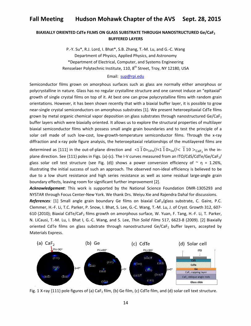
Semiconductor films grown on amorphous surfaces such as glass are normally either amorphous or
polycrystalline in nature. Glass has no regular crystalline structure and one cannot induce an “epitaxial”
growth of single crystal films on top of it. At best one can grow polycrystalline films with random grain
orientations. However, it has been shown recently that with a biaxial buffer layer, it is possible to grow
near‐single crystal semiconductors on amorphous substrates [1]. We present heteroepitaxial CdTe films
grown by metal organic chemical vapor deposition on glass substrates through nanostructured Ge/CaF2
buffer layers which were biaxially oriented. It allows us to explore the structural properties of multilayer
biaxial semiconductor films which possess small angle grain boundaries and to test the principle of a
solar cell made of such low‐cost, low‐growth‐temperature semiconductor films. Through the x‐ray
diffraction and x‐ray pole figure analysis, the heteroepitaxial relationships of the mutilayered films are
determined as [111] in the out‐of‐plane direction and <1 1 0>CdTe//<1 1 0>Ge// 1 10 in the in‐
plane direction. See 111 poles in Figs. (a)‐(c). The I‐V curves measured from an ITO/CdS/CdTe/Ge/CaF2/
glass solar cell test structure (see Fig. (d)) shows a power conversion efficiency of ~ η = 1.26%,
illustrating the initial success of such an approach. The observed non‐ideal efficiency is believed to be
due to a low shunt resistance and high series resistance as well as some residual large‐angle grain
boundary effects, leaving room for significant further improvement [2].
Acknowledgement: This work is supported by the National Science Foundation DMR‐1305293 and
NYSTAR through Focus Center‐New York. We thank Drs. Weiyu Xie and Rajendra Dahal for discussions.
References: [1] Small angle grain boundary Ge films on biaxial CaF2/glass substrate, C. Gaire, P.C.
Clemmer, H.‐F. Li, T.C. Parker, P. Snow, I. Bhat, S. Lee, G.‐C. Wang, T.‐M. Lu, J. of Cryst. Growth 312, 607‐
610 (2010); Biaxial CdTe/CaF2 films growth on amorphous surface, W. Yuan, F. Tang, H.‐F. Li, T. Parker,
N. LiCausi, T.‐M. Lu, I. Bhat I, G.‐C. Wang, and S. Lee, Thin Solid Films 517, 6623‐8 (2009). [2] Biaxially
oriented CdTe films on glass substrate through nanostructured Ge/CaF2 buffer layers, accepted by
Materials Express.
Fig. 1 X‐ray 111 pole figures of (a) CaF2 film, (b) Ge film, (c) CdTe film, and (d) solar cell text structure.

Fall Meeting Hudson Mohawk Chapter of the AVS Sept. 28, 2015
15
EXPERIMENTAL STUDY OF SPATIAL CONFINEMENT EFFECT ON ACOUSTIC PHONON TRANSPORT IN SIO2 NANORODS USING ULTRAFAST PUMP‐PROBE SPECTROSCOPY
Xiaohan Shen, Yukta P. Timalsina, Toh‐Ming Lu, Masashi Yamaguchi
Department of Physics, Applied Physics, and Astronomy
Rensselaer Polytechnic Institute, Troy NY 12180
Email: [email protected] The thermal management in nanoscale electronic devices is urgently necessary. Theoretical predictions
indicate the acoustic transport in nanostructures with dimensions comparable to phonon wavelength
behaves fundamentally different compare to bulk materials due to the spatial confinement.
Consequently, the thermal transport, which is an ensemble of acoustic transport of phonons with
various wavelengths, is affected to some extent due to spatial confinement effect on acoustic phonon
transport. We use the continuum model to calculate the acoustic phonon dispersion relation of
cylindrical SiO2 nanorods with various dimensions, and find the phonon (frequency below 100 GHz)
group velocity in SiO2 nanorod with diameter smaller than 200 nm is reduced from the sound speed of
bulk SiO2. Experimental investigation of the spatial confinement effect on the longitudinal acoustic
phonon transport in cylindrical SiO2 nanorods with diameter equals 200 nm is conducted using ultrafast
pump‐probe spectroscopy. Vertically grown SiO2 nanorod arrays on a substrate with various array
periods are used to investigate the periodicity effect on acoustic phonon transport. The transient
reflectivity signals show two types of contributions. First contribution is independent of the array pitch,
and the other contribution depends on the pitch. The former contribution is assigned to be the
mechanical vibration mode of individual SiO2 nanorod. For the latter contribution, the period of the
oscillation is found to be close to the round trip time of surface acoustic wave propagates between two
adjacent nanorods. Considering the optical detection mechanism of acoustic waves propagate on the
sample, some coupling between the surface acoustic wave and the longitudinal strain propagates
through the nanorod is necessary for the acoustic modes to be detected. We propose a model of the
coupling between the surface acoustic wave and longitudinal wave propagates along the nanorods. In
addition, a novel technique of narrowband acoustic phonon spectroscopy with center frequency
continuously tunable throughout hundreds of GHz regime is developed, which can be applied in the
future to investigate the frequency dependent acoustic phonon transport in nanostructures with a high
spectral resolution.

Fall Meeting Hudson Mohawk Chapter of the AVS Sept. 28, 2015
16
CHARACTERIZATION OF Cu(In, Ga)Se2 WITH VARYING Ga RATIOS
Isaiah MoriA, Jesse ClaypooleA, Bernadette PeaceA, Neville SunA, Pradeep HaldarA, Harry EfstathiadisA
A SUNY Colleges of Nanoscale Science and Engineering, 257 Fuller Road, Albany, NY 12203, USA B Angstrom Sun Technologies Inc., 31 Nagog Park, Acton, MA 01720, USA
Email: [email protected]
Cu(In1‐x,Gax)Se2 (CIGS) is one of the leading materials in the study of thin film photovoltaics. Key features of CIGS based devices are a tunable bandgap (1.0 – 1.7eV), lower fabrication cost, and a current world efficiency record of 21.7%. These factors have made CIGS solar thin films a promising cost‐effective technology. CIGS bulk layers of varying Ga content (described as Ga/(In+Ga) ratios) were deposited onto molybdenum (Mo) coated soda‐lime glass substrates. In order to further understand the effect of Ga content on film quality, Ga ratios ranging from 0.29 – 0.414 (as determined by x‐ray florescence spectroscopy (XRF)) were used, as the mechanisms responsible for performance limitations with high Ga content CIGS devices are not well understood. Ga grading in the CIGS layer is responsible for creating higher bandgaps toward the front and rear contacts while lowering the bandgap in the middle of the CIGS layer. Additionally, a wider Ga grading dip in the CIGS layers tend to lead to form larger crystal grains in regions of lower Ga/(In+Ga) ratios. Moreover, the surface roughness of the CIGS layers was found to decrease from 51.2nm to 41.0nm with increasing Ga/(In+Ga) ratios. However, the surface roughness also decreases depending on how deep the Ga grading dip occurs in the bulk layer.
Figure 1. SIMS profile of all four samples, Ga/(In+Ga) ratios are as follow: A (0.29), B (0.321), C (0.353), D (0.414).
0
0.1
0.2
0.3
0.4
0.5
0.6
0.7
0 500 1000 1500 2000 2500
Ga/
(Ga+
In)
Depth (nm)
Combined Ga/(Ga+In) Data
A
B
C
D

Fall Meeting Hudson Mohawk Chapter of the AVS Sept. 28, 2015
17
CREATION OF FRONTWALL CdS/CdTe PHOTOVOLTAICS USING NICKEL SUBSTRATES AS THE BACK
CONTACT LAYER
L.J. Seewald, P.‐Y. Su*, S.B. Zhang, G.‐C. Wang, I. Bhat*, and T.‐M. Lu
Department of Physics, Applied Physics and Astronomy
*Department of Electrical Computer and System Engineering
Rensselaer Polytechnic Institute, 110, 8th Street, Troy, NY 12180, USA
Email: [email protected]
Commercially available CdTe photovoltaics traditionally are fabricated using the “backwall”
configuration. In the backwall configuration a transparent conducting oxide (TCO) coated piece of glass
is used as the substrate for device fabrication. This method of fabrication limits the CdTe film to a
polycrystalline texture. We have created CdS/CdTe photovoltaic devices in the “frontwall” method,
which allows for different textures of CdTe to be grown depending on the substrate used. For testing
purposes, initial experiments have been conducted using polycrystalline nickel substrates. The structure
for these devices is ITO/CdS/CdTe:As/ZnTe:As/poly‐Ni (Fig. 1). The 50 nm thick ZnTe layer in this
structure is heavily As‐doped and used as a buffer layer for conduction between the poly‐Ni substrate
and the 2 m thick CdTe layer [1]. Both ZnTe and CdTe were grown using metal organic chemical vapor
deposition, CdS was grown with thermal evaporation, and the ITO was grown with sputter deposition. A
power‐conversion efficiency of η = 1.4% has been achieved using this device structure. This efficiency is
much lower than commercially available devices, though these devices use a CdCl2 treatment which has
not yet been applied to our devices. Our work demonstrates that the fabrication of our “frontwall”
device structure is feasible and the substrate can serve as the back side electrode contact. If near single‐
crystal metal substrates are employed to grow near single‐crystal CdTe [2] layer, the structure can lead
to possible high efficiency solar cells. Acknowledgements: This work is supported by the National
Science Foundation DMR‐1305293 and NYSTAR through Focus Center‐New York.
References: [1] CdTe/ZnTe/GaAs Heterostructures for Single‐Crystal CdTe Solar Cells. Peng‐Yu Su,
Chungho Lee, Gwo‐Ching Wang, Toh‐Ming Lu, and Ishwara B. Bhat. J. of Electronic Materials 43 (8),
2895‐2900 (2014). [2] Epitaxial growth of CdTe thin film on cube‐textured Ni by metal‐organic chemical
vapor deposition. C. Gaire, S. Rao, M. Riley, L. Chen, A. Goyal, S. Lee, I. Bhat, T.‐M. Lu, G.‐C. Wang. Thin
Solid Films 520, 1862–1965 (2012).
Fig 1: (a) I‐V test curves in dark (black line) and bright
(red curve) conditions and (b) Completed CdS/CdTe PV
device on a poly‐Ni substrate.
(a) (b)

Fall Meeting Hudson Mohawk Chapter of the AVS Sept. 28, 2015
18
EFFECT OF SURFACE TERMINATION ON THE GROWTH OF GRAPHENE ON Cu SINGLE CRYSTAL SUBSTRATES
Tyler R. Mowll1, Eng Wen Ong1, Parul Tyagi2, Zachary Robinson3, Carl A. Ventrice Jr.4
1University at Albany‐SUNY
2GLOBALFOUNDRIES 3College at Brockport‐SUNY 4SUNY Polytechnic Institute
Email: [email protected]
The most common technique for synthesizing single‐layer graphene films with large lateral dimensions is
chemical vapor deposition (CVD) on Cu foil substrates. The primary reasons for choosing Cu substrates
are the extremely low solubility of carbon in Cu, which allows a self‐limited growth of graphene, and the
relatively low cost of the Cu foil substrates. However, the transport properties of the CVD grown
graphene films are typically a couple of orders of magnitude lower than for graphene flakes
mechanically exfoliated from graphite. One of the reasons for the reduction in transport properties is
the presence of crystalline defects in the CVD grown films. These structural defects arise in part from the
multidomain structure of the Cu films. In order to achieve a better understanding of the influence of the
surface termination of the Cu substrate on the crystallization of graphene during the CVD growth
process, a systematic study of graphene growth on Cu(100), Cu(110), and Cu(111) crystals has been
performed. The growth process is performed in an ultra‐high vacuum (UHV) chamber that has been
modified to perform CVD growth at pressures as high as 100 mTorr. The precursor gas used is ethylene.
This growth procedure allows for the preparation of the clean surfaces in UHV, growth under typical
CVD conditions, and characterization of the surface structure in UHV, without exposing the sample to
atmospheric contaminants. Our results indicate that the Cu(111) surface has the lowest catalytic activity
of the three surfaces for the decomposition of ethylene. In fact, the decomposition rate is so low that
graphene growth is suppressed because of the sublimation of Cu at the elevated temperatures used to
grow the graphene. By using an Ar overpressure, it was found that graphene could be grown on that
surface. The surface symmetry of the Cu substrate has a strong influence on the rotational alignment of
the graphene grains as they nucleate on each surface. For Cu(111), single‐domain graphene growth can
be achieved for ethylene pressures of 5 mTorr or less. For both Cu(100) and Cu(110), a minimum of two
graphene domains is always observed.