MEDICAL ELECTRONICS LAB - sitttrkerala.ac.insitttrkerala.ac.in/misc/LabManual/MEL.pdf · Avoid use...
59
1 MEDICAL ELECTRONICS LAB
Transcript of MEDICAL ELECTRONICS LAB - sitttrkerala.ac.insitttrkerala.ac.in/misc/LabManual/MEL.pdf · Avoid use...

1
MEDICAL ELECTRONICS LAB
2
STATE INSTITUTE OF TECHNICAL TEACHERS TRAINING AND RESEARCH
GENERAL INSTRUCTIONS
Rough record and Fair record are needed to record the experiments conducted in the laboratory.
Rough records are needed to be certified immediately on completion of the experiment. Fair records are
due at the beginning of the next lab period. Fair records must be submitted as neat, legible, and complete.
INSTRUCTIONS TO STUDENTS FOR WRITING THE FAIR RECORD
In the fair record, the index page should be filled properly by writing the corresponding experiment
number, experiment name , date on which it was done and the page number.
On the right side page of the record following has to be written:
1. Title: The title of the experiment should be written in the page in capital letters.
2. In the left top margin, experiment number and date should be written.
3. Aim: The purpose of the experiment should be written clearly.
4.Apparatus/Tools/Equipments/Components used: A list of the Apparatus/Tools /Equipments
/Components used for doing the experiment should be entered.
5. Principle: Simple working of the circuit/experimental set up/algorithm should be written.
6. Procedure: steps for doing the experiment and recording the readings should be briefly
described(flow chart/programs in the case of computer/processor related experiments)
7. Results: The results of the experiment must be summarized in writing and should be fulfilling the
aim.
8. Inference : Inference from the results is to be mentioned.
On the Left side page of the record following has to be recorded:
1. Circuit/Program: Neatly drawn circuit diagrams/experimental set up.
2. Design: The design of the circuit/experimental set up for selecting the components
should be clearly shown if necessary.

3
3. Observations: i) Data should be clearly recorded using Tabular Columns.
ii) Unit of the observed data should be clearly mentioned
iii) Relevant calculations should be shown. If repetitive calculations are needed, only show a sample
calculation and summarize the others in a table.
4. Graphs : Graphs can used to present data in a form that show the results obtained, as one or more of
the parameters are varied. A graph has the advantage of presenting large
amounts of data in a concise visual form. Graph should be in a square format.
GENERAL RULES FOR PERSONAL SAFETY
1. Always wear tight shirt/lab coat , pants and shoes inside workshops.
2. REMOVE ALL METAL JEWELLERY since rings, wrist watches or bands, necklaces, etc. make excellent
electrodes in the event of accidental contact with electric power sources.
3. DO NOT MAKE CIRCUIT CHANGES without turning off the power.
4. Make sure that equipment working on electrical power are grounded properly.
5. Avoid standing on metal surfaces or wet concrete. Keep your shoes dry.
6. Never handle electrical equipment with wet skin.
7. Hot soldering irons should be rested in its holder. Never leave a hot iron unattended.
8. Avoid use of loose clothing and hair near machines and avoid running around inside lab .
TO PROTECT EQUIPMENT AND MINIMIZE MAINTENANCE:
DO: 1. SET MULTIRANGE METERS to highest range before connecting to an unknown source.
2. INFORM YOUR INSTRUCTOR about faulty equipment so that it can be sent for repair.
DO NOT: 1. Do not MOVE EQUIPMENT around the room except under the supervision of an instructor.

4
Experiment No: 1.1
BIO AMPLIFIER
Aim:
To design and setup a bioamplifier for a gain of 10and to calculatethe CMMR.
Objectives:
On completion of this experiment the student will be able to:
1. Identify instrumentation amplifier
2. Set up the circuit on bread board
3. To calculate common mode gain AC, Difference mode gain Ad and CMRR.
Equipment / components:
Sl no Name and Specification Quantity required
1. Bread board 1
2. Variable Power Supply 1
3. D.S.O. 1
4. Dual Power Supply (+/- 15 V) 1
5. µA 741C 3
6. Resistor(10K) 4
7. Resistor( 5K) 3
Theory:
The bio amplifier is commonly called as instrumentation amplifier. The circuit
consists of 3 Op-amps. The first two amplifiersact as the input stage and provide the high input
impedance. The second stage is a differential amplifier and it amplifies the differential signal
from the first stage and provides the gain. The main features of instrumentation amplifier are
high gain, high input resistance, high CMRR.

5
These amplifiers are very useful in instrumentation systems which measures pressure,
temperature, humidity, light intensity and weight etc. Most of the instrumentation systems use
a transducer in a bridge circuit. Instrumentation amplifier facilitates the amplification of
potential difference that takes place due to the imbalance of a bridge according to a change in
physical quantity.
Procedure:
1. Design and set up a bio amplifier circuit on bread board.
2. Set up V1 =0.5V dc and V2 =0.4 V dc and measure output voltage on
DSO.
3. Calculate the difference mode gain Ad.
4. Feed V1 = V2=0.5V and observe the output voltage.
5. Calculate the common mode gain Ac.
6. Calculate CMRR from the relation CMRR =20 log Ad/ AC.
Circuit Diagram:

6
Design:
Voltage gain A = R3/R2(1+ 2R1/Rg)
Total gain A = 10, take gain for first stage A1 = 5 and second stage A2 =2
A1 = (1+ 2R1/Rg) =5,
2R1/Rg = 4choose Rg = 5KΩ then R1= 10KΩ
A2 =R3/R2= 2 choose R2= 5KΩ then R3=10KΩ
Observations:
Difference mode: V1 = 0.5V V2 = 0.4V Vod = …. V
Common mode: V1 = 0.5V V2 = 0.5V Voc = …. V
Calculations:
Difference modegain Ad = Vod/ 0.1V = …….
Common modegain Ac= Voc/ 0.5V = ……
CMRR = 20 log (Ad/ AC) = …….. dB
Result:
Designed and set up a bio amplifier for a gain of 10 and calculated the CMRR.
Inference:
The circuit has high CMRR so it can be used as bio amplifier in the biopotential
measuring circuits. The noise elimination capability is very high for bioamplifiers.

7
Experiment No: 1.2
PHASE DETECTOR
Aim:
Familiarize PLL IC 565 and study its functional characteristics.
Objectives:
On completion of this experiment the student will be able to:
1. ExplainPLL IC 565 and its main features and applications.
2. Set up the circuit on bread board
3. Observe the lock range and capture range.
Equipment / components:
Sl no Name and Specification Quantity required
1. Bread board 1
2. Function Generator 1
3. D.S.O. 1
4. Dual Power Supply (+/- 15 V) 1
5. µA 741C 3
6. Resistors 6
Theory:
PLL mainly consists of a phase detector, a Low Pass Filter and a VCO. Phase detector compares
the input frequency with the feedback frequency. Output of phase detector is a DC voltage
proportional to the phase difference between frequencies. Low pass filter removes high
frequency noise. The dc voltage controls VCO frequency.The filter also helps in to establish the

8
dynamic characteristic of the PLL circuit. The output frequency of the VCO is directly
proportional to the input DC level. The VCO frequency is compared to the input frequencies and
it is adjusted till it is equal to the input frequencies. The phase locked loop clearly goes through
three stages: free running, capture and phase lock.
PROCEDURE:
1. Check all the components.
2. First set up the IC 565 circuit from a ±10V supply.
3. By adjusting the potentiometer set the free running frequency to 2.5
KHz.
4. Then apply a square wave of peak-to-peak amplitude 10V input
between pins 2& 3.
5. Increase the input from 1Hz to higher frequencies slowly. Upto some
point output frequency is same as free running frequency then it follows the input
frequency.
6. Note point at which the output frequency follows input frequency as
fc1
7. Again increase the input frequency and at some point output again
switches back to free running frequency that point is noted as fl2.
8. The next step is to decrease the frequency from there and note the
lock frequency as fc2 and unlock frequency as fl1.
9. Then calculate the lock range and capture range.

9
Circuit Diagram:
Design:
Let V+ = 10 V V- = -10V
Let Free running frequency F0 = 1.2/ (4R1C1) = 2.5 KHz
Take C1 = 0.01 µF Then R1 = 12K
Take C3 = 0.01 µF and C2 =10 µF
Theoretical values : FL = +/- (8F0/V) = +/- (8 x 2.5 x 103)/(10-(-10) =+/- 1KHz
Fc = +/- (FL)1/2/ (2 x 3.14 x 3.6 x 103 x C2)1/2 = 66.6Hz
Observation:
FL1 =…….Hz FL2 =…….Hz
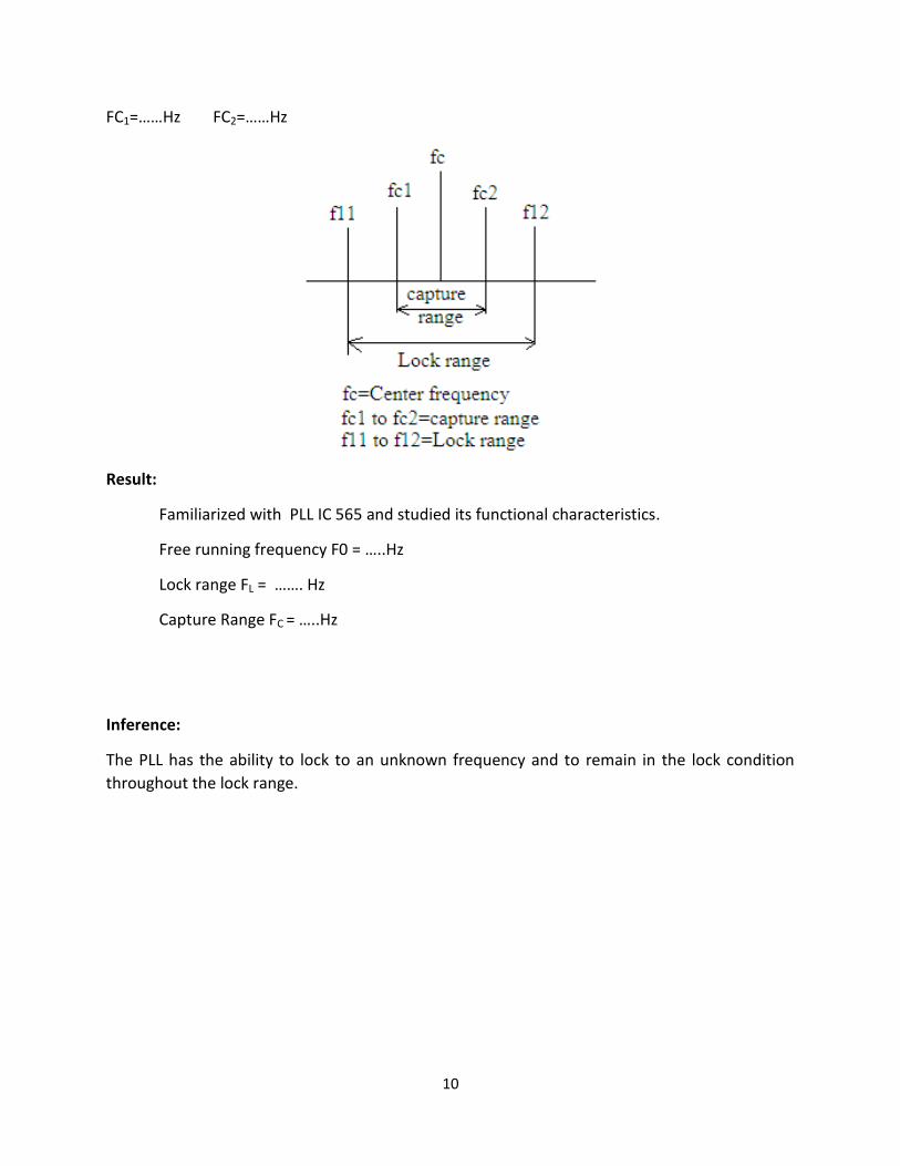
10
FC1=……Hz FC2=……Hz
Result:
Familiarized with PLL IC 565 and studied its functional characteristics.
Free running frequency F0 = …..Hz
Lock range FL = ……. Hz
Capture Range FC = …..Hz
Inference:
The PLL has the ability to lock to an unknown frequency and to remain in the lock condition
throughout the lock range.

11
Experiment No: 1.3
NOTCH FILTER
Aim:
To design and setup a notch filter for a notch out frequency of 50Hz and plot the
frequency response characteristics.
Objectives:
On completion of this experiment the student will be able to:
1. Design and implement a notch filter circuit.
2. Set up the circuit on bread board and to analyze the output
3. To plot the frequency response on graph sheet.
Equipment / components:
Sl no Name and Specification Quantity required
1. Bread board 1
2. Function Generator 1
3. D.S.O. 1
4. Dual Power Supply (+/- 15 V) 1
5. µA 741C 1
6. Resistor(33KΩ) 2
7. Resistor(15KΩ) 1
8. Capacitors (0.1µF) 2
9. Capacitor( 0.2 µF) 1
Theory:
Filter is a frequency selective circuit that passes electric signals of specified band of
frequencies and attenuates the signals of frequencies outside the band. Notch filter is actually a

12
narrow band reject filter. This is because of its higher Q (> 10) it is commonly used for the
rejection of a single frequency. The most commonly used notch filter is the twin –T network.
This network consists of two T networks, one consisting of two resistors and a capacitor and the
other consisting of two capacitors and a resistor.
At the notch frequency, the filter shows maximum attenuation and the filter will pass all
other frequency signals. The notch out frequency is given by
fN = 1 / 2πRC
The passive twin T-network has a relatively low figure of merit Q. To increase the value
of Q, a voltage follower network is connected at the end of the twin T network. They are
generally used in communication and bio medical instruments for eliminating the undesired
frequencies like power line frequency.
Procedure:
1. Setup circuit on the bread board.
2. Connect the ±15V power supply.
3. Feed a 1 Vppsinusoidal input and vary the frequency from 10Hz to 1 KHz
4. Vary the frequency of the sine wave in steps and note down the corresponding output
voltage.
5. Plot the frequency response curve on a graph sheet.
6. Find the notch frequency.

13
Circuit Diagram:
Design:
Notch frequency FN= 1/2πRC
FN= 50Hz, Let C = 0.1µF
R =1/(2 x 3.14 x50 x 0.1 x 10-6) = 31847Ω≈33KΩ
Observations:
Vi= 1Vpp
F ( Hz) Log F V0 in Volts Gain (dB)

14
Graph:
Result:
Designed and set up a notch filter for a notch out frequency 50Hz.
fN (from the graph) = …… Hz
Inference:
The notch filter is able to reject a single frequency. So it can be used for power line
noise rejection in biomedical instruments.

15
Experiment No: 1.4
Familiarisation of IC 4051
Aim:
To demonstratehe use of IC 4051as multiplexer or demultiplexer.
Objectives:
On completion of this experiment the student will be able to:
1. Identify MUX IC4051
2. Use the IC for multiplexing or demultiplexing signals.
Equipment / components:
Sl no Name and Specification Quantity required
1. Bread board 1
2. Function Generator 1
3. D.S.O. 1
4. Fixed power supply +5V 1
5. IC 4051 1
Theory:
The IC 4051 is an 8-channel analog multiplexer/demultiplexer with three address inputs (S0 to
S2), an active LOW enable input (E), eight independent inputs/outputs (Y0 to Y7) and a common
input/output (Z). The device contains eight bidirectional analog switches, each with one side
connected to an independent input/output (Y0 to Y7) and the other side connected to a
common input/output (Z). With E LOW, one of the eight switches is selected by S0 to S2. With E
HIGH, all switches are in the high-impedance OFF-state, independent of S0 to S2. If break
before make is needed, then it is necessary to use the enable input.

16
VDD and VSS are the supply voltage connections for the digital control inputs (S0 to S2, and E).
The VDD to VSS range is 3 V to 15 V. The analog inputs/outputs (Y0 to Y7, and Z) can swing
between VDD as a positive limit and VEE as a negative limit. VDD VEE may not exceed 15 V.
Unused inputs must be connected to VDD, VSS, or another input. For operation as a digital
multiplexer/demultiplexer, VEE is typically ground. VEE and VSS are the supply voltage
connections for the switches.
The IC 4051 cab be used for applications like analog and Digital Multiplexing and
Demultiplexing, A/D and D/A Conversion , Signal Gating etc.
Procedure:
1. Set up the circuit as shown in figure to operate as multiplexer.
2. Connect VDD to +5 V supply and VSS and VEE to ground.
3. Feed the Y0 to Y7 pins with LOW(0V) or HIGH(5V) input combinations.
4. Connect the enable pin to ground.
5. Verify the output Z by selecting the appropriate input using select lines S0 to S2.
6. By interchanging the input and output the circuit can be used as demultiplexer.
(Note: The experiment can be repeated analog input.)

17
Circuit Diagram:
PIN DIAGRAM IC 4051

18
Observation:
Result:
Studied the IC 4051 and set up the mux/ demux circuit and verified the output.
Inference:
The IC can be used for multiplexing or demultiplexing digital or analog signals.The IC can
also be used for Time Division Multiplexing of the various lead outputs of bio potential
recorders.

19
Experiment No: 1.5
THRESHOLD DETECTOR
Aim:
To design and setup a threshold detector circuit using op-amp for a voltage level of 5V.
Objectives:
On completion of this experiment the student will be able to:
1. Identifycomparator circuits.
2. Set up the circuit on bread board and to analyze the output
Equipment / components:
Sl no Name and Specification Quantity required
1. Bread board 1
2. Function Generator 1
3. D.S.O. 1
4. Dual Power Supply (+/- 15 V) 1
5. µA 741C 1
6. Variable power supply
1
Theory:
A threshold detector is commonly called as a comparator. It is a circuit which compares
a signal voltage on one input of an op-amp with a known voltage called the reference voltage
on the other input. It is an open loop op-amp with 2 analog inputs and a digital output. The
output may be positive or negative depending on which input is larger. It is of two types:
Inverting and non –inverting comparator.
20
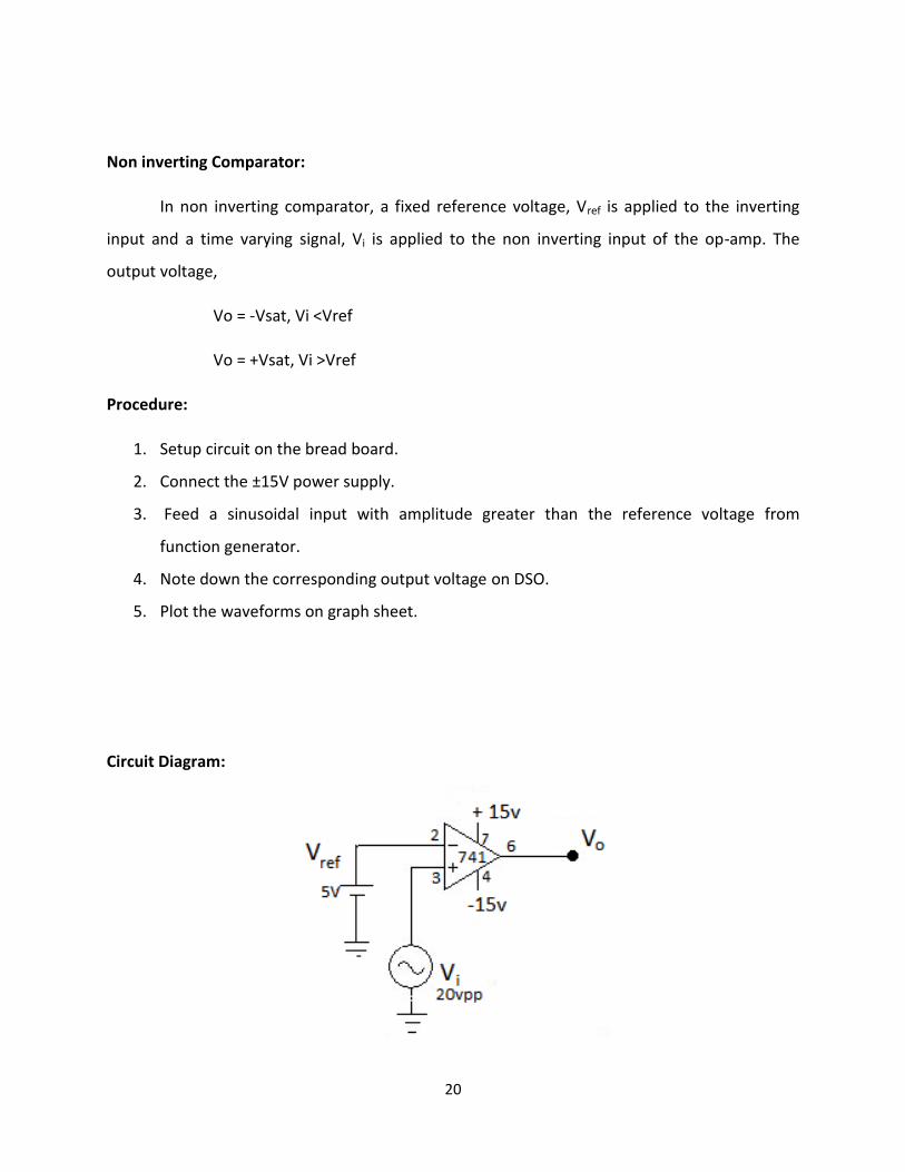
Non inverting Comparator:
In non inverting comparator, a fixed reference voltage, Vref is applied to the inverting
input and a time varying signal, Vi is applied to the non inverting input of the op-amp. The
output voltage,
Vo = -Vsat, Vi <Vref
Vo = +Vsat, Vi >Vref
Procedure:
1. Setup circuit on the bread board.
2. Connect the ±15V power supply.
3. Feed a sinusoidal input with amplitude greater than the reference voltage from
function generator.
4. Note down the corresponding output voltage on DSO.
5. Plot the waveforms on graph sheet.
Circuit Diagram:

21
Graph:
Result:
Set up a threshold detector circuit and plotted the waveforms.
Inference:
A threshold detector can be used to identify whether the amplitude of any unknown
signal exceeds a particular voltage level.In medical field the circuit can be used as QRS detector
in Defibrillators and pacemakers.

22
Experiment No: 1.6
THERMISTOR CHARACTERISTICS
Aim:
To determine the resistance vs.temperature characteristics of a thermistor.
Objectives:
On completion of this experiment the student will be able to:
1. Identify Thermistors.
2.Analyze the characteristics of a thermistor.
Equipment / components:
Sl no Name and Specification Quantity required
1. Bread board 1
2. Variable power supply 1
3. Thermistor 1
4. Ammeter(0 - 50mA) 1
5. Voltmeter (0 – 30V) 1
6. Thermometer 1
7. Water bath 1
8. Heater 1
9. Resistor(470Ω) 1

23
Theory:
Thermistors are the temperature sensitive resistors that exhibit a variation in resistance
with temperature. In other words electrical resistance of a thermistor will varywhen it is placed
in an environment of changing temperature.The characteristics study of thermistor provides
information about how its resistance changes with the changes in temperature.
Based on the relationship between the resistance and temperature thermally
sensitiveresisters are of two types, one the posistor and its resistance increases with increasing
temperature(positive temperature coefficient) and second the thermistor and its resistance
decreases with increasing temperature(negative temperature coefficient). Thermistors are very
essential in temperature measurement and they are made up of the oxides of certain metals
like manganese, cobalt and nickel which have negative temperature coefficient of resistance.
They are formed into rods, discs, washers andbeadto suite various applications.
The application of thermistor includes cardiac output measurements, continuous
measurement of skin and core body temperature, blood flow measurement and respiratory
measurement. They are also used as resistance thermometers in low temperature
measurements.
Procedure:
1. Take water in a container and place over the heater.
2. Immerse thermistor and thermometer in the water bath.
3. Set up the measuring circuit on the bread board.
4. Switch on the heater.
5. Measure the temperature on the thermometer from room temperature to
98oC and note down the corresponding resistance of thermistor.
6. Switch off the heater, and then take reading in decreasing order of
temperature in an interval of 10o C.
7. Plot a graph of temperature on X-axis and Resistance on Y-axis. This graph
shows the characteristics of thermistor.

24
Circuit Diagram:
Observations:
Temp (oC) Resistance(Ω)
(Up)
Resistance(Ω)
(Down)
Graph:

25
Result:
Set up the circuit and plotted the characteristics of thermistor.
Inference:
Temperature and resistance relationship is non-linear for a thermistor.(i.e.
characteristics of thermistor are non-linear).

26
Experiment No: 1.7
SKIN CONTACT IMPEDENCE
Aim:
To set up a circuit for measuring the skin contact impedance.
Objectives:
On completion of this experiment the student will be able to:
1. Identify the electrodes for bio potential measurements
2. Explain the need of using jelly while using electrodes.
3. Set up and measure the contact impedance.
Equipment / components:
Sl no Name and Specification Quantity required
1. Function Generator 1
2. Bread board 1
3. ECG Electrodes 3
4. Resistor(1 K) 1
5. Resistor (47K) 1
6 DSO 1
Theory:
The bio electric events are usually measured by means of metallic electrodes placed on
the surface of the body. The electrical activity generated by various muscles and nerves within
the body is conducted to the electrode through the body tissues. It reaches electrodes through

27
the skin electrode transition and is then conducted by direct wire connection to the input
circuit of the recording machines. The impedance at the electrode skin interface comes in the
overall circuitry of the recording machine. Hence the skin electrode impedance is significant of
the final recording. Skin electrode impedance is called as the contact impedance and is of value
greater than the electrical impedance of the body tissue as measured beneath the skin. The
outer horny layer of the skin is responsible for the bulk of skin contact impedance.Jelly is used
in order to increase the contact between the subject’s skin and the skin electrodes. The skin
contact impedance is reduced on the application of the jelly.
Procedure:
1. Set the function generator output at 2Vpp.
2. Set up the circuit with switch in position 1 and measure the voltage
across 1k by varying the input frequency from 0 to 100Hz.
3. Repeat step 2 after applying jelly
4. Set up the circuit with switch in position2 and measure the voltage
across Zcby varying input frequency from 0 to 100Hz
5. Calculate I=V1/1K and calculate Zc=Vzc/I
6. Plot the frequency Vs impedance graph.
Circuit Diagram:

28
Observations:
Without jelly With jelly
F(Hz) V1(V) I(mA) Vzc(V) Zc(KΩ) F(Hz) V1(V) I(mA) Vzc(V) Zc(KΩ)
Graph:

29
Result:
Set up the circuit and measured the skin contact impedance with and without jelly.
Maximum impedance without jelly = …….. Ω
Minimum impedance without jelly = …….. Ω
Maximum impedance with jelly = …….. Ω
Minimum impedance with jelly = …….. Ω
Inference:
The skin contact impedance is high without jelly so use jelly to reduce the contact
impedance while measuring biopotentials.

30
Experiment No: 1.8
LDR CHARACTERISTICS
Aim:
Todetermine the resistance characteristics of a given LDR.
Objectives:
On completion of this experiment the student will be able to:
1. Identify LDRs.
2. Analyze the characteristics of LDR.
Equipment /components:
Sl no Name and Specification Quantity required
1. Multimeter 1
2. Bread board 1
3. LDR 1
4. Ammeter(0-100)mA 1
5. Voltmeter(0-30)V 1
6 DC source(0-30)V 1
7. Bulb 1
Theory:
A photo resistor is an electronic component whose resistance decreases with increasing
incident light intensity. It can also be referred to as a light- dependent resistor (LDR), or
photoconductor. A photoresistor is made of a high resistance semiconductor. If light falling on
the device is of high enough frequency, photons absorbed by the semiconductorgive bound
electrons enough energy to jump into conduction band. The resulting free electrons (and its
hole partner) conduct electricity there by lowering resistance.

31
Cadmium selinide or cadmium sulphide are mainly used to construct LDRs. Simple
cadmium sulphide cells have a wide range of resistance from less than 100ohm in bright light to
in excess of 10Mohm in darkness. The cells are also capable of reacting to a broad range of
frequencies including infra-red (IR), visible light and ultra violet. They are often found on street
lights as automatic on/off switches. In biomedical field it is used in photo plethismography.
Procedure:
1. Setup circuit on the bread board.
2. Vary the DC input in steps from 0V to 30V
3. Note down the ammeter, voltmeter and ohmmeterreadings.
4. Calculate the input power Pin = V x I.
5. Plot a graph of Power on X-axisandResistance on Y-axis. This graph
shows the characteristics of LDR.
Circuit Diagram:

32
Observations:
V(volts) I(mA) Pin(mW) R(Ω)
Graph:
Result:
Set up the circuit and plotted the characteristic curve.
Dark resistance of LDR = …………. MΩ
Inference:
The resistance – light intensity relationship is non-linear for a LDR.(i.e. characteristics of
LDRis non-linear).
33
Experiment No: 1.9
ACTIVE BAND PASS FILTER
Aim:
To design and setup an active band pass filter with pass band ranging from 2 KHz to 4 KHz.
Objectives:
On completion of this experiment the student will be able to:
1. Set up a band pass filter using HPF and LPF sections
2. Analyze the frequency response of filters.
Equipment/components:
Sl no Name and Specification Quantity required
1. Bread board 1
2. D.S.O. 1
3. Dual Power Supply (+/- 15 V) 1
4. µA 741 2
5. Capacitors( .01µF) 2
6. Resistors(10KΩ) 4
7. Resistors(3.9KΩ,8.2 KΩ) 1 each
8. Function Generator 1
Theory:
Filter is a frequency selective circuit that passes electric signals of specified band of
frequencies and attenuates the signals of frequencies outside the band. Band pass filter is a
circuit which provides zero attenuation to the flow of signals in the specified band and must
provide maximum attenuation outside this band. It can be formed by cascading a High Pass
Filter and Low Pass Filter section. If the HPF and LPF are of the first order, then the band pass
filter will have roll off rate of -20dB / decade. For the high pass section, the lower cutoff
frequency fL=½(πR2C2). For the low pass section, the upper cutoff frequency is fH = ½( πR1C1).

34
The overall gain of the band pass filter circuit is the product of gains produced by low pass and
high pass filter section.
Procedure:
1. Design and set up a band pass filter circuit.
2. Feed a 1 V p-p sinusoidal input and vary the frequency from 100Hz to 20 KHz
3. Note down the values of output voltage at different frequencies.
4. Plot the frequency response and calculate the band width.
Circuit Diagram:
Design:
Low pass section: fH=1/(2πR1C1)
fH=4KHz Choose C1=0.01μF
R1= 1/(2 x 3.14 x 4 x 103 x 0.01 x 10-6) = 3.9 KΩ
A1=2= (1+Rf/Ri)=2, Rf/Ri=1
Choose Ri= Rf =10KΩ
High pass section: fL= 1/(2πR2C2)
fL= 2KHzChoose C2=0.01μF
R2= 1/(2 x 3.14 x 2 x 103 x 0.01 x 10-6)= 7.9KΩ ≈ 8.2KΩ

35
A2=2= (1+R’f/R’i) R’f/R’i=1
Choose R’i= R’f =10KΩ
Observation:
Vi= 1Vpp
F ( Hz) Log F V0 ( Volts) Gain (dB)
Graph:
Result:
Designed and set up an active band pass filter for a pass band of 2KHz to 4KHz.
Bandwidth from the graph = …….. Hz
Inference:
A bandpass filter can be used as a frequency selective circuit.

36
Experiment No: 1.10
FLASH ADC (3-bit)
Aim:
To design and set up a 3- bit flash Analog to Digital Converter.
Objectives:
On completion of this experiment the student will be able to:
1. Explain ADC
2. set up flash ADC circuit
3. study quad op amp IC LM324
Equipment / components:
Sl no Name and Specification Quantity required
1. Bread board 1
2. Dual Power Supply (+/-15 V) 1
3. Variable Power Supply 1
4. LM324 7
5. IC 7486 2
6. Resistor 1KΩ 8
7. Resistor 470Ω 3
8. LEDs 3
Principle:
An analog to digital converter accepts an analog input and produces a binary output. An n-bit
analog to digital converter has 2n discrete outputs. The flash ADC uses 2n –1 comparators and 2n

37
identical resistors. The circuit is so called because of its fastness. A 3 bit ADC consists of 8 op-
amp comparators and an 8 to 3 line priority encoder.It compares the input voltage with respect
to a number of reference voltages and the comparator sets or resets as the input varies. The
output combinations of comparators are given to a priority encoder set by an EX-OR gate circuit
as shown in the figure.
Procedure:
1. Check all the components.
2. set up the comparator part of circuit as shown in figure on the
breadboard.
3. Give 15V supply to the op-amp circuit.
4. Connect a variable supply of 0-4V as the input.
5. Verify the comparator output voltages for all steps of input. (For
example when the input voltage crosses 0.5V, output at A switches to 0V and when
the input voltage crosses 3.5V all comparator outputs are 0V).
6. Connect LEDs in series with current limiting resistor to X0, X1& X2
outputs.
7. By varying input voltage observe output conditions.
Circuit diagram:
PIN DIAGRAM LM324

38
PIN DIAGRAM 7486

39
Design:
A B C D E F G X2 X1 X0
1
1
1
1
1
1
1
0
1
1
1
1
1
1
0
0
1
1
1
1
1
0
0
0
1
1
1
1
0
0
0
0
1
1
1
0
0
0
0
0
1
1
0
0
0
0
0
0
1
0
0
0
0
0
0
0
0
0
0
0
1
1
1
1
0
0
1
1
0
0
1
1
0
1
0
1
0
1
0
1
From the truth table it can be found that
X0=ABCD’EFG
X1=BFD’
X2=D’

40
Observation:
Input
voltage(V)
output
X2 X1 X0
Result:
Designed and set up a flash ADC circuit and verified the output.
Inference:
Flash ADC can be used to convert analog signal to digital signal. The circuit is fastbecause all the
comparators are working simultaneously.

41
Experiment No: 1.11
PRECISION RECTIFIERS
Aim:
To setup a half wave and full wave precision rectifier and plot the waveforms.
Objectives:
On completion of this experiment the student will be able to:
1. Identify precision rectifier circuits
2. Set up the circuit on bread board and to analyze the output
3. To plot the waveforms on graph sheet.
Equipment /components:
Sl no Name and Specification Quantity required
1. Bread board 1
2. Function Generator 1
3. D.S.O. 1
4. Dual Power Supply (+/- 15 V) 1
5. µA 741 2
6. Resistors(100KΩ) 5
7. Diodes 1N4001 2
Theory:
The limitation of ordinary diode rectifier is that they are not able to rectify signals with
amplitude less than the diode cut in voltage. Precision rectifiers are able to rectify any input
signal even if they are of very small amplitude.
Half wave rectifier:
An inverting voltage follower can be converted into an ideal half wave rectifier by
adding two diodes. When input voltage is positive, output becomes negative and the diode D1
gets forward biased. At this moment diode D2 is reverse biased. When input becomes negative,

42
output becomes positive and diode D2 gets forward biased. So for a sinusoidal input the circuit
give an inverted output for the –ve half cycles.
Full wave rectifier:
The full wave rectifier circuit is also called absolute value circuit. Here the first amplifier
works as an inverting amplifier always and second amplifier works in two modes depending
upon the polarity of the input voltage, one inverting mode and the other in non-inverting
mode. When input is positive diode D1 conducts and diode D2 does not conduct. Both
amplifiers are now working in the inverting mode. When the input becomes negative diode D1
turns off and diode D2 turns on. Then the first amplifier is working as inverting and the second
as non-inverting amplifier. So irrespective of the polarity of the input voltage output V0 turns to
be positive always.
Procedure:
1. Setup the half wave circuit on the bread board.
2. Connect the ±15V power supply.
3. Apply input sine wave from function generator with zero offset voltage.
4. Observe the input and output waveforms in a DSO in DC coupled mode.
5. Verify the output by applying input voltage below 0.7V.
Repeat the same steps for full wave rectifier circuits.
Circuit diagram: -
(1) Half wave inverting rectifier:

43
2) Full wave rectifier:
Graph:
Result:
Set up half wave and full wave precision rectifier circuits and plotted the waveforms.
Inference:
The circuit can rectify any signal including small amplitude signals having amplitude
lessthan 0.7V. S they are suitable for biomedical applications.

44
Experiment No: 1.12
PATIENT ISOLATION CIRCUIT
Aim:
To set up a patient isolation circuit using opto-coupler IC MCT2E.
Objectives:
On completion of this experiment the student will be able to:
1. Explain the patient isolation techniques
2. Identify opto-coupler IC MCT2E
3. set up the circuit
Equipment / components:
Sl no Name and Specification Quantity required
1 Bread board 1
2 D.S.O 1
3 Variable Power Supply 1
4 Dual Power Supply (+/- 15 V) 1
5 µA 741 1
6 Capacitors( .1µF, 4.7µF) 1 each
7 Resistors(100Ω, 220Ω, 10KΩ,
100KΩ)
1 each
8 potentiometer(4.7KΩ). 1
9 PPG module 1

45
Principle:
MCT2E is an opto isolator chip, which is often used to provide isolation and to avoid any
electrical connection between the input and output stages. The prominent components in
MCT2E are a phototransistor and an LED. The phototransistor is made of silicon material and is
activated by the LED made of Germanium Arsenide. The output light of the LED is infrared and
the intensity is directly proportional to the potential applied between its two leads. In circuits,
where optical isolation is required between two stages, the output of the first stage is given to
theLED of MCT2E andthe photo transistor inside the chip transduces the emitted light in to a
proportional collector current. This is given as the input to the second stage, thus providing
electrical isolation. By means of providing optical isolation between input and output,
interference due to leads and other such artifacts can be avoided. Opto-couplers usually finds
applications in medical circuits, where patient safety is of much importance.
Procedure:
1. Setup the Circuit using MCT2E as shown in the circuit diagram.
2. Connect the end of PPG module from your body on the circuit.
3. Observe the output waveform in DSO and study the isolation function by using
separate ground for input and output circuit.
Circuit Diagram:

46
Result:
Set an application circuit of MCT2E and verified the output.
Inference:
MCT2E can be used as an isolation circuit .Even without any physical contact a signal
applied at the input can be reproduced at the output.

47
Experiment No.1.13
SAMPLE AND HOLD CIRCUIT
Aim:
To design and setup a discrete sample and hold circuit using op-amp.
Objectives:
On completion of this experiment the student will be able to:
1. explain the sampling theorem
2. set up a sample and hold circuit.
Equipment / components:
Sl no Name and Specification Quantity required
1 Bread board 1
2 D.S.O 1
3 µA 741C 2
4 BFW10 1
5 Capacitor 82 nF 1
6 Diode 1N4148 1
Principle:
The sample and hold circuit samples an input signal and holds onto the last sampled
value, until the input is sampled again. The circuit mainly consists of a sampler or a switching
element and a holding capacitor. In the circuit JFET used acts as the switching component. The
input signal is given to the drain of the JFET through a voltage follower and sampling high
frequency is given to the gate of JFET, through a diode. When the voltage at the gate is zero,
the JFET turns on and the capacitor charges to the input voltage. When the voltage at the gate
is negative, the JFET turns off. As the capacitor has no discharge path due to the high

48
impedance at the output of the voltage follower circuit, it holds the last sampled voltage. When
the JFET is again turns on the capacitor charges to the new input voltage. Thus sampling and
holding of the input signal occurs.
Procedure:
1. Check all the components.
2. Set up the discrete sample and hold circuit from a 15V supply.
3. Use dual output function generator to apply input and sampling
frequency simultaneously.
4. Set the input at 1 KHz, 4V peak to peak sine wave and sampling
square wave at 10 KHz, 8V peak to peak. Ensure that the negative gate voltage of
BFW10 is always less than 4V.
5. Then observe the input and outputs waveforms in a DSO.
Circuit diagram:

49
Graph:
Result:
Set up a sample and hold circuit and plotted the input output waveforms.
Inference:
The minimum sampling frequency should be twice the input signal.

50
Experiment No: 1.14
STUDY OF AD590
Aim :
Study AD590 and Plot voltage vs. temperature graph and calculate the sensitivity.
Objectives:
On completion of this experiment the student will be able to:
1. Identify AD590
2. Analyze the characteristics of AD590
Equipment / components:
Sl no Name and Specification Quantity required
1. Bread board 1
2. Function Generator 1
3. D.S.O. 1
4. Dual Power Supply (+/- 15 V) 1
5. µA 741 2
6. AD 590 1
Theory:
AD590 is a temperature transducer. It converts temperature to electrical signals. It
shows a response of 1µA/oK. This circuit converts this change in current with temperature to an
equivalent change in voltage per oC. The voltage developed is in µV. It is developed across the
potentiometer connected in series with the AD590 and is equivalent to temperature in Kelvin
scale. In order to get the output in terms of Celsius scale, a reference voltage of 273mV is
subtracted using a differential amplifier. The 273mV is obtained from the potential divider
circuit connected across a forward biased diode. Thus at the non-inverting terminal of the op-
amp we give a voltage, which is temperature dependent, and at the inverting terminal we give

51
a positive voltage of 0.273V. Then the output voltage of differential amplifier circuit gives
reading corresponding to temperature in Celsius scale.
Procedure:
1. Check all the components.
2. First set up the voltage divider part of circuit from a 5V supply. Then set the output
of the potential divider to 0.273V using the potentiometer.
3. Then wire AD590 in series with a potentiometer from the 5V supply.
4. Then measure the room temperature with a thermometer and set the voltage across
the potentiometer corresponding to that voltage (For e.g. if the room temperature is
30oC set the voltage as 37mV. i. e 300mV-273mV).
5. Then wire the differential amplifier circuit from a 15V supply and verify that the
output is corresponding to the oC reading (for e.g. for 30oC output 300mV).
6. After that, insert the AD590 in a test tube and keep it in a beaker, half filled with
water, and vary its temperature by heating the beaker using Bunsen burner.
7. Measure the temperature by keeping a thermometer near to AD590 in the test tube.
8. Measure and note down output voltage corresponding to the input temperature
using a DMM.
9. Plot a graph of temperature on X-axisandvoltage on Y-axis.
10. Calculate sensitivity from the graph.
52
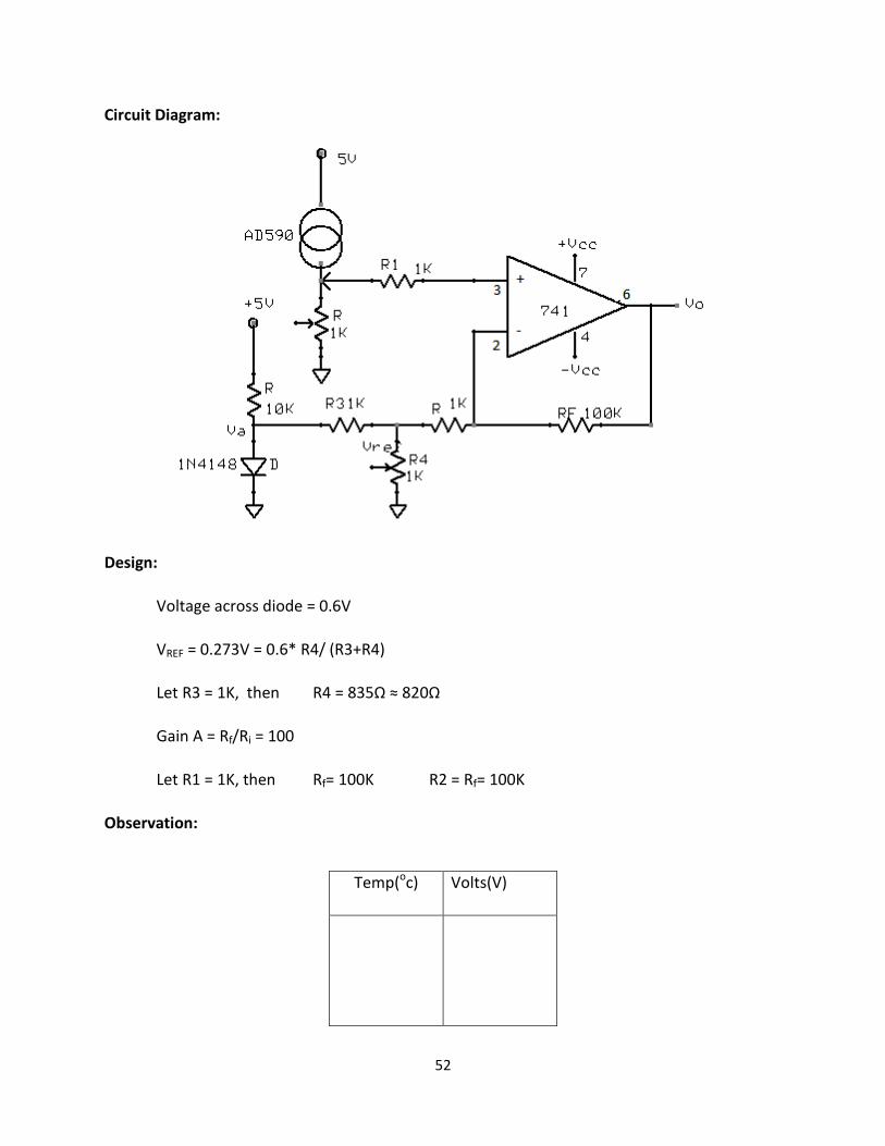
Circuit Diagram:
Design:
Voltage across diode = 0.6V
VREF = 0.273V = 0.6* R4/ (R3+R4)
Let R3 = 1K, then R4 = 835Ω ≈ 820Ω
Gain A = Rf/Ri = 100
Let R1 = 1K, then Rf= 100K R2 = Rf= 100K
Observation:
Temp(oc) Volts(V)

53
Graph:
Result:
Studied the IC AD590 and plotted the voltage vs. temperature graph.Calculated the
sensitivity.
Sensitivity from the graph =……………V/oC.
Inference:
IC AD590 can be used to design circuit for measuring temperature.

54
Experiment No: 1.15
STUDY OF ECG, EEG AND EMG ELECTRODES
Aim:
To Study different types ofsurface electrodes used for bio potential measurements.
Objectives:
On completion of this experiment the student will be able to:
1. Identify various electrodes
2. Explain their characteristics, features and applications
Equipment / components:
Sl no Name and Specification Quantity required
1. ECG electrodes(limb, suction
floating, disposable)
1 each
2. EEG electrodes (needle, pad ,
plastic cup)
1 each
3. EMG electrodes(needle,
capacitive)
1 each
Theory:
Bioelectric events have to be picked up from the surface of the body before they can be
put into the amplifier for subsequent record or display. This is done by using electrodes.
Electrodes make a transfer from the ionic conduction in the tissue to the electronic conduction
needed for measurements. Two types of electrodes are used in practice – surface electrodes
and deep seated electrodes. The surface electrodes pick up th signal from the tissue surface
without damaging them and the deep seated electrodes indicate the potential inside the live
tissue or cell. Various electrodes used for ECG, EEG and EMG measurement are explained
below:

55
ECG Electrodes
1. Suction Cup Electrode
In this type of electrode only the rim actually contacts the skin. One of the difficulties in
using plate electrode is the possibility of electrode slippage or movement. This also occurs with
the suction cup electrode of a sufficient length of time. A number of attempts were made to
overcome this problem, including the use of adhesive backing a surface resembling a nutmeg
greater that penetrate the skin to lower the contact impedance and reduce the likelihood of
slippage.Suction cup electrode is commonly used to record the unipolar chest leads.It has high
contact impedance as only the rim of electrode is in contact with the skin.Electrode jelly forms
the vacuum seal.
2. Limb Electrodes
The most common surface electrode used for recording ECG are limb electrodes. These
are either circular or rectangular in shape. The material used is German silver, Nickel silver or
nickel plated steel. They are applied to the surface of the body with electrode jelly. Its contact
impedance is nearly 2 to 5 KΩ when measured at 10HZ. Electrodes are held in position by elastic
straps. Limb electrodes are generally preferred for use during surgery. Limb electrodes are not
56
suitable for use in long term patient monitoring because the long flowing leads are
inconvenient to the patient.
3. Floating Electrodes
Limb electrodes generally suffer from motion artifacts due to relative motion at the
interface between the metal electrode and adjacent layer of electrode jelly. The interface can
be stabilized by the use of floating electrode sin which the metal electrode does not make
contact directly with the skin. The electrode consists of a light weight metaled screen or plate
held away from the subject by a flat washer which is connected to the skin. Floating electrode
can be recharged i.e., jelly in the electrodes can be replenished if desired.
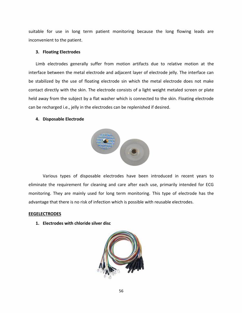
4. Disposable Electrode
Various types of disposable electrodes have been introduced in recent years to
eliminate the requirement for cleaning and care after each use, primarily intended for ECG
monitoring. They are mainly used for long term monitoring. This type of electrode has the
advantage that there is no risk of infection which is possible with reusable electrodes.
EEGELECTRODES
1. Electrodes with chloride silver disc

57
The most commonly electrodes for measuring EEG are the electrodes with chloride
silver discs of size 6 to 8 mm diameters.Contact with the scalp is made via an electrolytic paste
through a washer of soft felt.They have ac resistance varying from 3 to 20KΩ.
2. Needle electrode
Small needle electrodes are usedfor carrying out special EEG studies.They are like
needle and are inserted into the skull for taking EEG.Silver ball or pellet electrode covered with
asmall cloth pad is useful when electrical activity is to be recorded from the exposed cortex,but
they have high dc resistances.
3. Pad electrode
It is made from a silver rod belled out at the end and padded with sponge,or similar
material, contained in gauze.It is screwed into an insulated mount and held in place on the
head with a rubber cap.
4. Plastic cup electrode

58
Another type of EEG electrode consists of multiple fine chloride silver wires fixed in a
rigid plastic cup.The plastic cup is fixed to thescalp with an adhesive.It is filled with jelly through
a hole in the top.In this electrode, contact with the tissue is made via an electrolyte bridge so
that jelly in contact with the electrode metal is not disturbed by scalp movement.
EMG ELECTRODES
1. Needle electrodes
The most common electrodes used for taking EMG are needle electrodes. The material used
for needle is generally stainless steel. The mono polar needle electrode consists of a Teflon
coated stainless steel wire which is bare only at the tip.Bipolar needle electrodes contain two
insulated wires within a metal cannula. The two wires are bared at the tip and provide the
contacts to the patient. The cannula acts as the ground. Bipolar electrodes are electrically
symmetrical and have no polarity sense.
2. Capacitive type electrodes
Capacitive type biomedical electrodes have also been used for EMG recordings from the
surface of the skin.The anodizedaluminium electrodes were not found suitable on a long term

59
basis because the dielectric film breaks down in thepresence of saline in the sweat.Capacitance
values of 800pF for a 12.5mm diameterelectrode are typical.
Result:
Studied different types of electrodes used for bio potential measurement.
Inference:
Surface electrodes are easy to use but there are possibilities of artifacts, drift and
baseline wandering. Due to risk of cross infections it is better to use disposable electrodes.