Measuring the Jitter of Clock Signal
12
AC 2011-409: MEASURING THE JITTER OF CLOCK SIGNAL Chao Li, Florida A&M University Dr. Chao Li is currently working at Florida A&M University as an assistant professor in Electronic En- gineering Technology. He is teaching Electronic and Computer Engineering Technology Courses. He ob- tained his BSEE degree from Xi’an Jiaotong University and MSEE degree from University of Electronic Science and Technology of China. He received his PHD in EE from Florida International University. He is an IEEE Member and a Member in ASEE. His research interests include signal processing, biometrics, embedded microcontroller design, application of new instructional technology in classroom instruction. Antonio J. Soares, Florida A&M University Antonio Soares was born in Luanda, Angola, in 1972. He received a Bachelor of Science degree in Electri- cal Engineering from Florida Agricultural and Mechanical University in Tallahassee, Florida in December 1998. He continued his education by obtaining a Master of Science degree in Electrical Engineering from Florida Agricultural and Mechanical University in December of 2000 with focus on semiconductor de- vices, semiconductor physics, Optoelectronics and Integrated Circuit Design. Antonio then worked for Medtronic as a full-time Integrated Circuit Designer until November 2003. Antonio started his pursuit of the Doctor of Philosophy degree at the Florida Agricultural and Mechanical University in January 2004 under the supervision of Dr. Reginald Perry. Upon completion of his PhD, Dr. Soares was immediately hired as an assistant professor (Tenure Track) in the Electronic Engineering Technology department at FAMU. Dr. Soares has made many contributions to the department, from curriculum improvements, to ABET accreditation, and more recently by securing a grant with the department of education for more than half a million dollars. c American Society for Engineering Education, 2011 Page 22.1054.1
Transcript of Measuring the Jitter of Clock Signal

AC 2011-409: MEASURING THE JITTER OF CLOCK SIGNAL
Chao Li, Florida A&M University
Dr. Chao Li is currently working at Florida A&M University as an assistant professor in Electronic En-gineering Technology. He is teaching Electronic and Computer Engineering Technology Courses. He ob-tained his BSEE degree from Xi’an Jiaotong University and MSEE degree from University of ElectronicScience and Technology of China. He received his PHD in EE from Florida International University. Heis an IEEE Member and a Member in ASEE. His research interests include signal processing, biometrics,embedded microcontroller design, application of new instructional technology in classroom instruction.
Antonio J. Soares, Florida A&M University
Antonio Soares was born in Luanda, Angola, in 1972. He received a Bachelor of Science degree in Electri-cal Engineering from Florida Agricultural and Mechanical University in Tallahassee, Florida in December1998. He continued his education by obtaining a Master of Science degree in Electrical Engineering fromFlorida Agricultural and Mechanical University in December of 2000 with focus on semiconductor de-vices, semiconductor physics, Optoelectronics and Integrated Circuit Design. Antonio then worked forMedtronic as a full-time Integrated Circuit Designer until November 2003. Antonio started his pursuit ofthe Doctor of Philosophy degree at the Florida Agricultural and Mechanical University in January 2004under the supervision of Dr. Reginald Perry. Upon completion of his PhD, Dr. Soares was immediatelyhired as an assistant professor (Tenure Track) in the Electronic Engineering Technology department atFAMU. Dr. Soares has made many contributions to the department, from curriculum improvements, toABET accreditation, and more recently by securing a grant with the department of education for morethan half a million dollars.
c©American Society for Engineering Education, 2011
Page 22.1054.1
DSP Based Jitter Measuring Method
Introduction
In the past decade, jitter has become a very important parameter to describe the quality of clock
pulse signal. In digital systems, clock frequency has become higher and higher. With the clock
frequency increasing, the tiny changes in rising or falling edges will have a bigger impact on the
system performance, such as the integrity of the data, setup and hold time of the data, etc. The
concept of the jitter is described in the JEDEC Standard No.65 (EIA/JESD 65) as “the shift of
the controlled or affected edge in respect to its normal position”. IEEE has a similar definition
for jitter, which is “The short-term variations of the significant instances of a digital signal from
their ideal positions in time (where short-term implies these variations are of frequency greater
than or equal to 10Hz).”[1]
. This means that jitter is an unwanted phase modulation to the original
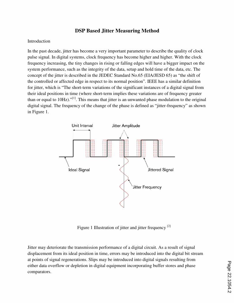
digital signal. The frequency of the change of the phase is defined as “jitter-frequency” as shown
in Figure 1.
Figure 1 Illustration of jitter and jitter frequency [2]
Jitter may deteriorate the transmission performance of a digital circuit. As a result of signal
displacement from its ideal position in time, errors may be introduced into the digital bit stream
at points of signal regenerations. Slips may be introduced into digital signals resulting from
either data overflow or depletion in digital equipment incorporating buffer stores and phase
comparators.
Page 22.1054.2
Measuring jitter
To measure the jitter we need to use jitter-measuring device. Jitter measuring device is a
specialized telecommunication measuring device. The International Telecommunication Union
(ITU) has set a series of standards for the communication measuring equipment manufactures.
As one of the telecommunication devices, jitter measuring device has to comply with the
international standards. The international standards related with measuring jitter are ITU-T.O171
and ITU-T.O172. The former one is used to measure the jitter in Plesiochronous Digital
Hierarchy (PDH) digital system. The latter one is used to measure the jitter in Synchronized
Digital Hierarchy (SDH) digital system. Other related standards are ITU-T G.823, ITU-T G.824,
which regulates the corresponding parameters and values in jitter measuring device in 2048kbit/s
and 144kbit/s PDH systems respectively.
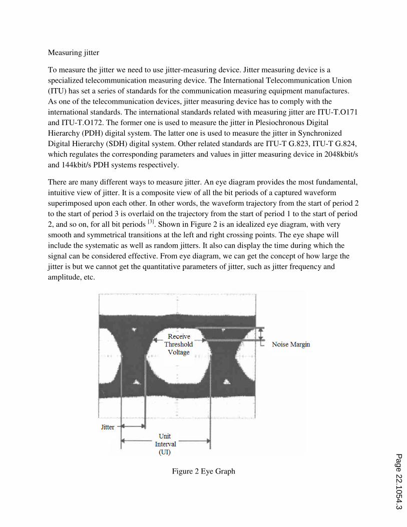
There are many different ways to measure jitter. An eye diagram provides the most fundamental,
intuitive view of jitter. It is a composite view of all the bit periods of a captured waveform
superimposed upon each other. In other words, the waveform trajectory from the start of period 2
to the start of period 3 is overlaid on the trajectory from the start of period 1 to the start of period
2, and so on, for all bit periods [3]
. Shown in Figure 2 is an idealized eye diagram, with very
smooth and symmetrical transitions at the left and right crossing points. The eye shape will
include the systematic as well as random jitters. It also can display the time during which the
signal can be considered effective. From eye diagram, we can get the concept of how large the
jitter is but we cannot get the quantitative parameters of jitter, such as jitter frequency and
amplitude, etc.
Figure 2 Eye Graph
Page 22.1054.3
With the development of digital technology, the digital method of measuring jitter becomes more
and more common. The main goal of digital method is to get the exact time for each period of
the clock signals. Then digital processing methods can be used to extract the information such as
jitter amplitude and jitter frequency from these data.
DSP based jitter measuring scheme
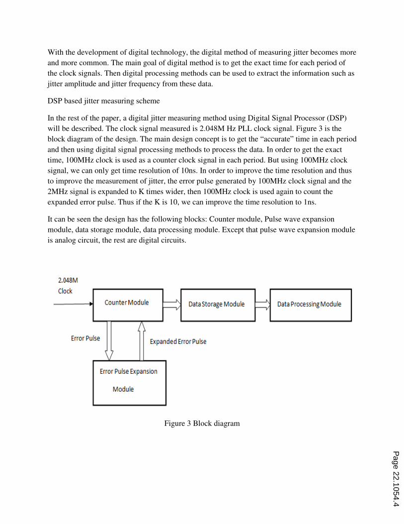
In the rest of the paper, a digital jitter measuring method using Digital Signal Processor (DSP)
will be described. The clock signal measured is 2.048M Hz PLL clock signal. Figure 3 is the
block diagram of the design. The main design concept is to get the “accurate” time in each period
and then using digital signal processing methods to process the data. In order to get the exact
time, 100MHz clock is used as a counter clock signal in each period. But using 100MHz clock
signal, we can only get time resolution of 10ns. In order to improve the time resolution and thus
to improve the measurement of jitter, the error pulse generated by 100MHz clock signal and the
2MHz signal is expanded to K times wider, then 100MHz clock is used again to count the
expanded error pulse. Thus if the K is 10, we can improve the time resolution to 1ns.
It can be seen the design has the following blocks: Counter module, Pulse wave expansion
module, data storage module, data processing module. Except that pulse wave expansion module
is analog circuit, the rest are digital circuits.
Figure 3 Block diagram
Page 22.1054.4

In the following, each module will be described in detail.
1. Counter Module:
The functions of the counter module are as follows:
• This module is used to count the number for the 2MHz in each period.
• It is also used to generate error signal. The error signal is generated when 100MHz signal
is used to count the 2MHz signal.
• It is used to count the expanded error signal.
• Generate the interfacing signals such WR, Clk_En for the data storage module.
• The counter values are outputted using 8 bit data bus to the data storage module.
• This module is implemented using XC95108 by Xilinx. XC9108 is a CPLD, which is
good for the design of digital circuit.
Figure 4 shows the corresponding waveforms in the counter module.
A. The 2.048MHz PLL Clock signal which needs to be measured.
B. The 1M Hz pulse wave after frequency division by 2.
C. The inverting waveform of (B)
D. 100MHz clock signal for the counter.
E. the error pulse generated at the rising edge when (B) waveform is counter using 100Mhz
F. the error pulse generated at the falling edge when (C) waveform is counted using
100MHz
G. The expanded waveform of (E)
H. The expanded waveform of (F)
In the counter module, 100MHz clock signal counts B, C, G, and H four channels of signals.
Thus there are four 8 bit counters in this module. The counter will start counting B waveform
when it is logic high such as during T1 and T5. Similarly, the counter will start counting G
waveform during T2 and T6, C waveform during T3 and T7, H waveform during T4 and T8.
Basically when the signal is logic high, the counter starts, while when the signal is logic low, the
counter holds the value. Since we can control how wide we want the error pulse to be expanded,
we will make sure that time during which G and H are logic high is less than that when B and C
are logic high. The module will output the counting values in the order of T1, T2, T3, T4, T5, T6,
T7, T8…….They use one 8 bit data bus by time-division to output to the data storage module.
Page 22.1054.5
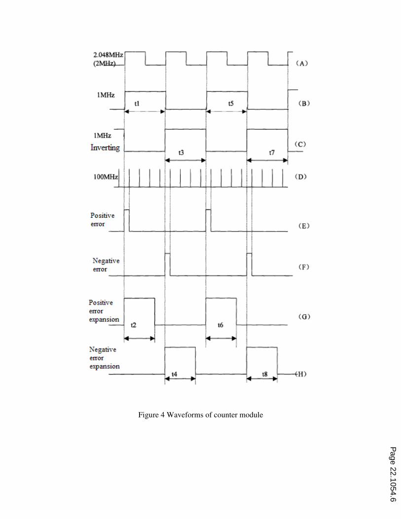
Figure 4 Waveforms of counter module
Page 22.1054.6
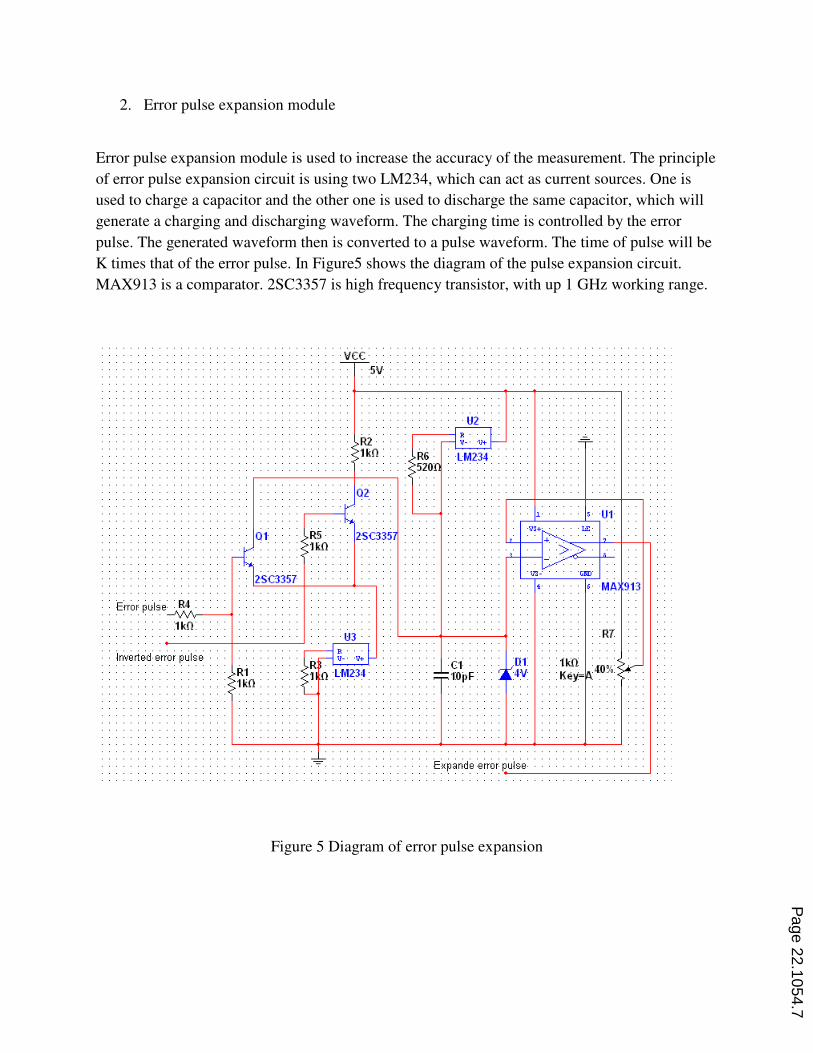
2. Error pulse expansion module
Error pulse expansion module is used to increase the accuracy of the measurement. The principle
of error pulse expansion circuit is using two LM234, which can act as current sources. One is
used to charge a capacitor and the other one is used to discharge the same capacitor, which will
generate a charging and discharging waveform. The charging time is controlled by the error
pulse. The generated waveform then is converted to a pulse waveform. The time of pulse will be
K times that of the error pulse. In Figure5 shows the diagram of the pulse expansion circuit.
MAX913 is a comparator. 2SC3357 is high frequency transistor, with up 1 GHz working range.
Figure 5 Diagram of error pulse expansion
Page 22.1054.7

The following is how the circuit works:
1. When there’s no error pulse
1.1 The current source will charge the capacitor C1 with current I2 (I2=0.1mA). Because
of the parallel Zener diode, the maximum charged voltage will be 4V.
1.2 The transistor Q2 is in the on state, so it provides a route to the current source.
Because if there is no such route, then it take several ns for the current source to reach
the steady state, then it make it impossible to be able to expand the error pulse, which
is only several ns long.
2. When the error pulse comes
2.1 Now the transistor is in on state, the capacitor C1 will discharge through current
source I1. But since I2 is still charging the capacitor C1, the real discharging current
is I1-I2.
The following figure shows the waveforms in different points.
(a) The voltage across C1
(b) The input error pulse to the base of transistor Q1
(c) The expanded error pulse.
In the (B) waveform in Figure 6, 10ns is added to the front of the error pulse. The reason to add
10 ns is because in the charging and discharging circuit, the beginning stage is not very linear.
We would like to avoid this area by adding 10ns to the error pulse. The selection of Vref is also
depends on the added 10ns pulse. In the debugging state, we can generate a pulse equal to 10ns.
The reference voltage Vref should be the minimum voltage in waveform (A). There will be no
output voltage at this moment. The output of the comparator will be the expanded error pulse.
The expansion factor
� =�ℎ� ��� � �ℎ ���� �����
�ℎ� ��� � ����ℎ ����� �����+ 1 =
�1 − �2
�2+ 1 =
�1
�2
The selection of the capacitor will satisfy that the 20ns error pulse will make the voltage change
about 2V.
Page 22.1054.8
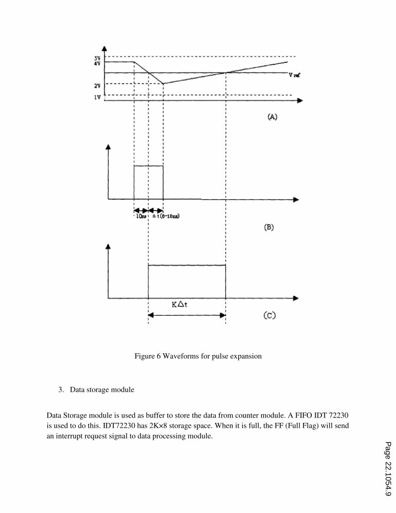
Figure 6 Waveforms for pulse expansion
3. Data storage module
Data Storage module is used as buffer to store the data from counter module. A FIFO IDT 72230
is used to do this. IDT72230 has 2K×8 storage space. When it is full, the FF (Full Flag) will send
an interrupt request signal to data processing module.
Page 22.1054.9
4. Data processing module
The core of the data processing module is a DSP TMS320F206 [4]
. This module is used to
process the data from counters and output the measurement of the jitter. The interrupt from the
FIFO is used to trigger an interrupt service routine to read out 2K data from FIFO. The other
communication DSP with external is through RS 232.
The following explains the algorithm in data processing module. The method to measure jitter is
to get the exact value in each period of the clock signal. In order to get the exact value, three data
from counter module is needed. From the Figure 6, t1, t2, t3, t4… represent the time for each
period (ns), T1, T2, T3, T4….T8 represent the counter value using 100MHz clock signal. From
Figure 4, it can be seen:
�1 = ��1 − 1� ∗ 10 + ����_���� + !��_����
Since !�� ���� � �1 = 10�� − ���� ���� ��3
���� ���� � �1 = �2 ∗#$
%&'()*+,) -(./ 0
�1 = �1 ∗ 10 + ��2 − �4� ∗#$
%&'()*+,) -(./ 0
This can be extrapolated to the following equation.
�) = �) + ��)2# − �)23� ∗ 10/�
Next, we are going to analyze the accuracy of the scheme. First we have the following three
assumptions:
(1) The accuracy of the 100MHz clock signal is high enough. In other words, error will not
introduced by the 100MHz crystal. In fact, the 100MHz crystal clock can reach the 4 digit
after the dot. Page 22.1054.10
(2) After frequency division, the 1MHz signal and its inverting signal, their edges are in line
with each other. There’s no time delay. This can also be met by putting time delay buffers
in the CPLD design.
(3) The linearity of the error pulse expansion circuit is good enough. This is been satisfied by
choose the right working region for the charging and discharging circuit.
Next using error pulse expansion K=20 as example to analyze the error of the jitter measuring
circuit. When the error pulse is 0.5ns, the expanded pulse will be 10ns. Suppose when the error
pulse is between 10ns and 20ns, the counter value will be 1.
Thus, When 105�� < � < 10�5 + 1���
The counter value is N, thus the maximum error generated by this jitter measuring scheme is 0.5
ns. If we don’t use the error pulse expansion circuit, the maximum error will be 10ns. From the
above discussion, it can be seen the error pulse expansion is a crucial part of the design.
Results
The following is the result of sinusoidal modulated jitter on the 2.048MHz clock signal. The
values represent the time of each period in ns.
467 463 460.5 461 464.5 469 …….499.5 503 507 511.5 514 518 515.5 510
507…….468.5 462.5 459……463.5 467 471……
From the data above, it can be seen the period of the 2MHz clock signal has peak values, which
in bold fonts. The jitter is sinusoidal modulated. We can get the frequency of the jitter from the
data. Jitter in each period is the absolute difference of actual time with 488 (1 UI). In practical
case, the jitter is random. Then it needs to get the spectrum of the jitter and get the amplitude of
the jitter for different frequency.
The following table shows when the frequency of the clock signal changes, the measured max
and min time for each period will also change.
Page 22.1054.11
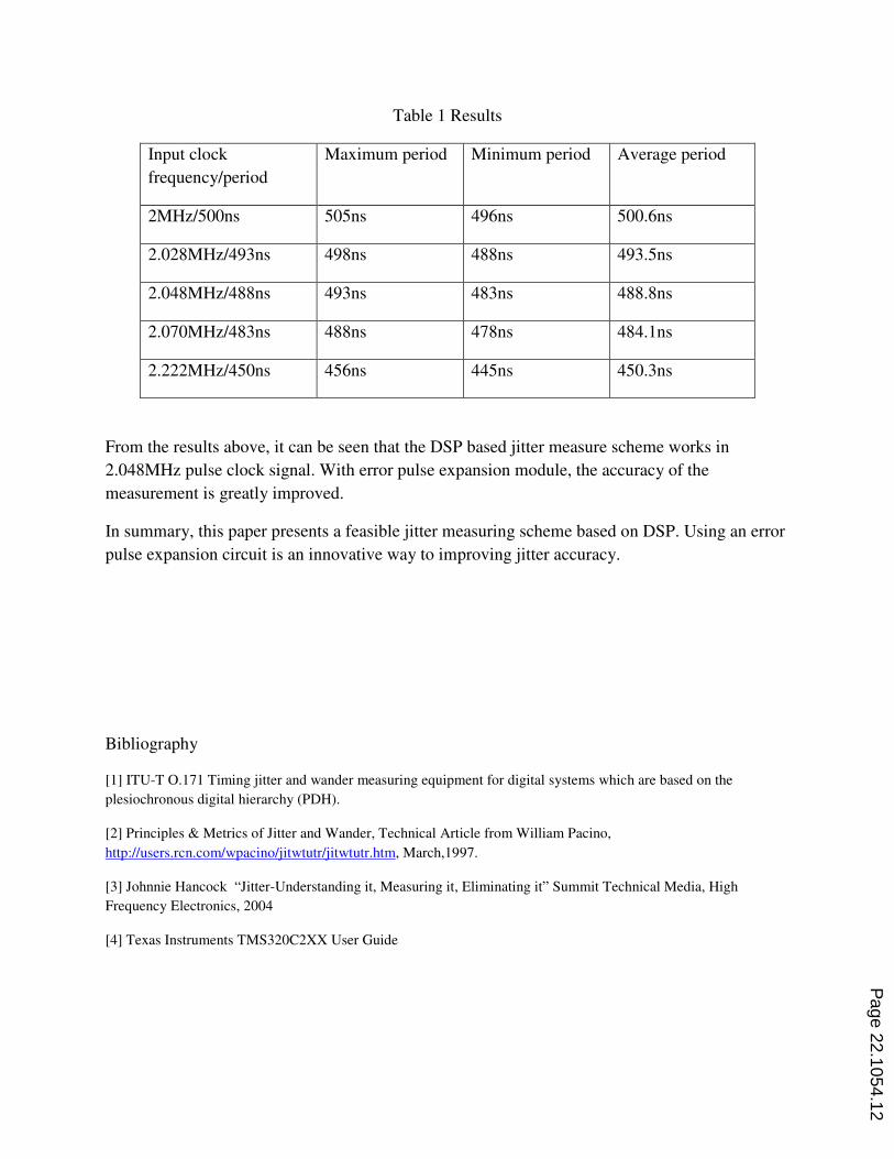
Table 1 Results
Input clock
frequency/period
Maximum period Minimum period Average period
2MHz/500ns 505ns 496ns 500.6ns
2.028MHz/493ns 498ns 488ns 493.5ns
2.048MHz/488ns 493ns 483ns 488.8ns
2.070MHz/483ns 488ns 478ns 484.1ns
2.222MHz/450ns 456ns 445ns 450.3ns
From the results above, it can be seen that the DSP based jitter measure scheme works in
2.048MHz pulse clock signal. With error pulse expansion module, the accuracy of the
measurement is greatly improved.
In summary, this paper presents a feasible jitter measuring scheme based on DSP. Using an error
pulse expansion circuit is an innovative way to improving jitter accuracy.
Bibliography
[1] ITU-T O.171 Timing jitter and wander measuring equipment for digital systems which are based on the
plesiochronous digital hierarchy (PDH).
[2] Principles & Metrics of Jitter and Wander, Technical Article from William Pacino,
http://users.rcn.com/wpacino/jitwtutr/jitwtutr.htm, March,1997.
[3] Johnnie Hancock “Jitter-Understanding it, Measuring it, Eliminating it” Summit Technical Media, High
Frequency Electronics, 2004
[4] Texas Instruments TMS320C2XX User Guide
Page 22.1054.12