Measurements 2: Network Analysis - CERN Accelerator School
46
Measurements 2: Measurements 2: Network Analysis Network Analysis Fritz Caspers CAS, Aarhus, June 2010
Transcript of Measurements 2: Network Analysis - CERN Accelerator School

Measurements 2:Measurements 2: Network Analysis Network Analysis
Fritz Caspers
CAS, Aarhus, June 2010
Contents
Scalar network analysis
Vector network analysis
Early concepts
Modern instrumentation
Calibration methods
Time domain (synthetic pulse)
Nonlinear analysis
Measurement of the 1 dB compression point
X‐parameters
Harmonic measurements
CAS, Aarhus, June 2010 2

Motivation
We want to determine the modulus and/ or modulus
and phase of the reflection and transmission coefficient of a DUT
We want to measure the complex and frequency dependent elements of the S‐matrix of 1, 2, 3,4 and
multi‐ports
In addition, we may be interested in nonlinear properties of our DUT (power sweep, harmonic analysis, X‐parameter)
Network analyzers meet these needs and furthermore they are also required for measurement
of the beam transfer function (BTF)CAS, Aarhus, June 2010 3

Scalar network analysis
For many measurement problems it is sufficient to know only the modulus of a complex transmission or
reflection coefficient.
A very simple measurement setup is depicted below
CAS, Aarhus, June 2010 4

Scalar network analysis
The detector may be a Schottky diode or any other
RF power measuring device such as a thermo‐ element producing a voltage between a junction of
two metals at different temperatures, or a resistor with a high temperature‐coefficient (thermistor)
The small signal response of a Schottky diode in the square law region (< ‐
10 dBm) delivers an output
voltage (U2
) proportional to the RF power
Often the source signal is amplitude modulated (on/off) with some low frequency e.g. 20 kHz for easier detection and suppression of DC drifts.
CAS, Aarhus, June 2010 5
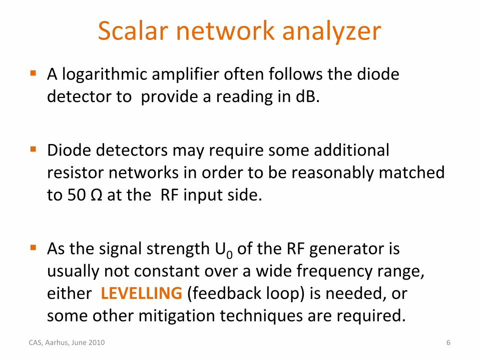
Scalar network analyzer
A logarithmic amplifier often follows the diode
detector to provide a reading in dB.
Diode detectors may require some additional resistor networks in order to be reasonably matched
to 50 Ω
at the RF input side.
As the signal strength
U0
of the RF generator is usually not constant over a wide frequency range,
either LEVELLING
(feedback loop) is needed, or some other mitigation techniques
are required.
CAS, Aarhus, June 2010 6

Scalar network analyzer
A resistive power divider may provide a reference
signal at any frequency and thus is very suitable for automatic level control (ALC) . The ratio U2
/U1
cancels amplitude variations of the generator during the
frequency sweep (feedback loop)
This type of power divider (see below) which is often applied for ALC , has however an insertion loss of 6 dB
CAS, Aarhus, June 2010 7

Scalar network analyzer
Alternatively, a directional coupler (coupling e.g. ‐10
dB) may be used, which has an even smaller insertion loss and better directivity as compared to
the resistive splitter
But in contrast to the resistive splitter, its limited frequency range may pose a problem in certain cases
CAS, Aarhus, June 2010 8
Note: wideband directionalcouplers are implemented instripline technology and thus
are BACKWARD couplers
U1
is a replica of the
forward travelling wave
and is used for leveling
and as reference

Scalar network analysis
If we want to measure simultaneously S11
and S21
with a scalar device, we need a dual directional coupler in order to separate the forward
and reflected wave respectively
CAS, Aarhus, June 2010 9
Note: ALC loop not
shown here
1
221 U
US
1
311 U
US

Scalar network analysis
The functionality of scalar network analysis in
transmission S21
can also be implemented using a spectrum
analyzer with tracking generator:
CAS, Aarhus, June 2010 10
With a mixer based detector
(superhet) we have a much
higher dynamic range as
compared to the direct diode
detector

Six port reflectometer
Only with power detectors is it possible to obtain the
full vectorial
information on the reflection coefficient (4 diode detectors at ports 3..6).Its operating concept is similar to sampling the modulus of some RF signal
along a RF measurement line at 4 positions
This configuration is known as a six‐port reflectometer:
CAS, Aarhus, June 2010 11
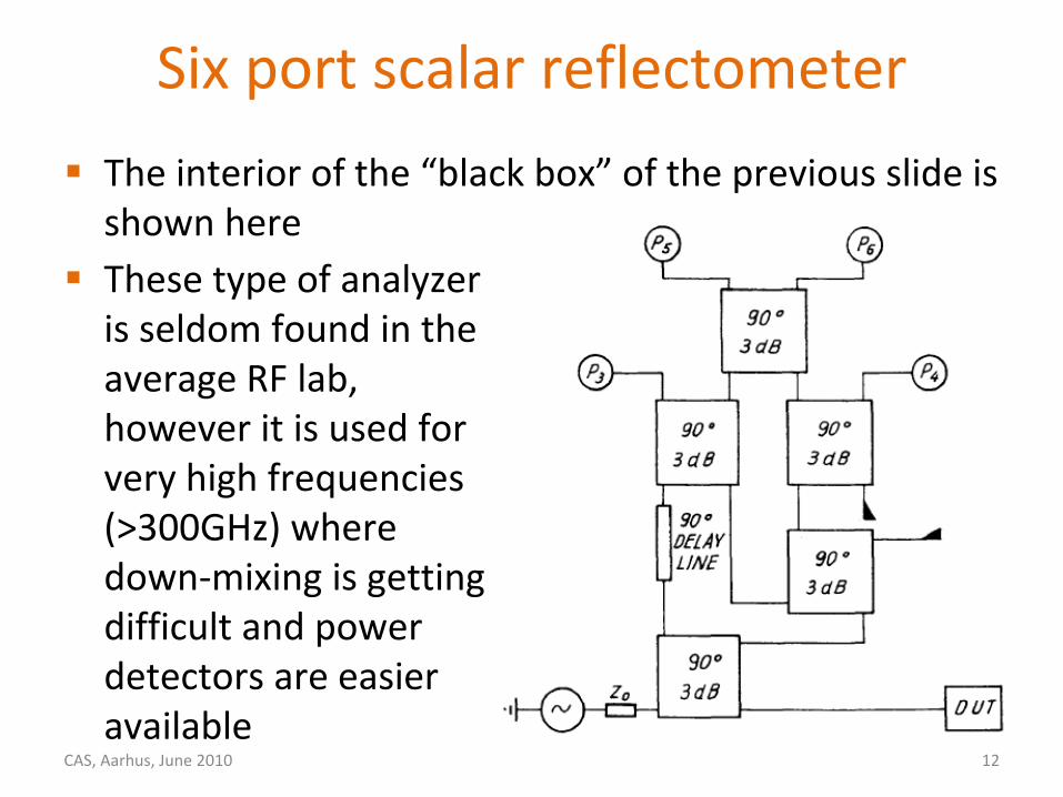
Six port scalar reflectometer
The interior of the “black box”
of the previous slide is shown here
CAS, Aarhus, June 2010 12
These type of analyzer is seldom found in the average RF lab,
however it is used for very high frequencies (>300GHz) where
down‐mixing is getting difficult and power
detectors are easier available

Bridge‐type methods for complex S‐ parameters
Remember the relation between S‐parameters and impedance of a lumped element:
Thus if our DUT is a single lumped element (series or shunt) we can determine the four elements of the
corresponding 2‐port S‐matrix and vice versa
CAS, Aarhus, June 2010 13
ZZZ
ZZZ
ZZZ
ZZZ
S
00
0
0
0
0
222
22
2
Bridge‐type methods for complex S‐ parameters
However, in the general case this conversion is not possible since we have no a priori information about
the content of our “black box”
(2‐port DUT)
In analogy to bridge measurements for impedance determination (Wheatstone bridge) there is a very similar technique for measuring S21
or S11 respectively at fixed frequency.
CAS, Aarhus, June 2010 14

For the transmission measurement a calibrated attenuator and phase shifter are set such that the
reading of the detector becomes minimal or zero (zero tuning). The S21
of the DUT then corresponds to the setting of the attenuator and the phase shifter
CAS, Aarhus, June 2010 15
Bridge‐type methods for complex S‐ parameters

In a similar way the reflection measurement bridge measures S11
from a variable attenuator and a variable short:
Certain vector volt meter based instruments use this method in an automated way for determination of
S21
and
S11CAS, Aarhus, June 2010 16
Bridge‐type methods for complex S‐ parameters

Vector network analyzer
Having discussed scalar two port measurement methods and spectrum analyzer techniques, it is just a
small step to arrive at the vector network analyzer (superhet VNA)
The VNA uses in principle two generators that are both variable in frequency but coupled via phase‐locked loop circuit such that they maintain a constant difference in
frequency which is exactly the intermediate frequency known from the usual superhet receiver
This IF contains the full phase and amplitude information of the RF signal to be measured
CAS, Aarhus, June 2010 17

Vector network analyzer
Simplified block diagram of a vector network
analyzer:
The three mixers in the figure are characteristic of many VNA´s and are in general well matched
CAS, Aarhus, June 2010 18

Vector Network Analyzer
Block diagram of a modern 2‐port VNA:
CAS, Aarhus, June 2010 19Courtesy: AnritsuDUT
ALC = automatic
level control
RF mixer/sampling
unit

Vector network analyzer
Modern 4‐port VNA:
In principle every multiport can be analyzed with a 2‐ port VNA, but this is tedious and time consuming for multiports like directional couplers or circulators.
CAS, Aarhus, June 2010 20

Time domain transform
The VNA delivers complex data in the frequency
domain. These data can be converted to time domain via FFT and vice versa:
The method is always applicable for linear and time invariant networks
CAS, Aarhus, June 2010 21
FFT

Time domain
When using the time domain option of the vector‐
network‐analyser we have two basic modes available:
•
The "low‐pass" mode and
•
The "band‐pass" mode
We will briefly discuss both of these modes in the following
CAS, Aarhus, June 2010 22

Time domain: low pass mode
The low‐pass mode can only be used for equidistant
sampling in the frequency domain (equidistant with
respect to DC), since the Fourier Transform of a
repetitive sequence of pulses has a line spectrum
with equidistant spacing of the lines including the
frequency zeroCAS, Aarhus, June 2010 23

Time domain: low pass mode
This implies that for a given frequency range and
number of data points the instrument must first work out the exact frequencies for the low‐pass‐ mode (done by using the soft‐key: set frequency Low‐pass).
Once these frequencies are defined, calibration (open, short, load for S11
and S22
) can be applied. For a linear time‐invariant system frequency and time
domain measurements are basically completely equivalent (except for signal to noise ratio issues)
and may be translated mutually via the Fourier transform.
CAS, Aarhus, June 2010 24

Time domain: weighting function
Note that the Fourier transform of a spectrum with
constant density over a given frequency range (rectangular spectrum) has a sin(t)/t0
characteristic in the time domain. This characteristic generates
undesired ringing ="side‐lobes":
CAS, Aarhus, June 2010 25

Time domain: weighting function
Thus an (amplitude) weighting function (=window) is
applied in the frequency domain before entering the FFT.
This weighting function is typically sin2
or Gaussian and helps to suppress strongly side‐lobes in the time‐
domain:
CAS, Aarhus, June 2010 26

Time domain: gating
Coming back to the example shown before:
If we are interested in the spectral content of the second peak only, we can apply a time domain gate
on this pulse (=part of the signal) and return to the frequency domain applying again the FFT.
CAS, Aarhus, June 2010 27

Time domain
When using the weighting and gating functions, keep in mind that
1.
The application of the weighting function (window)
2.
Gating is a non‐linear operation and thus gating may generate artificially frequency components which were not present before gating
CAS, Aarhus, June 2010 28

Time domain: S11
examples
Example of
application of the synthetic pulse
methode for S11 measurements with a
network analyzer:
Within the low‐pass mode we
can use the pulse and step
function respectively. The step
function is nothing else than
the integral over the pulse
response.CAS, Aarhus, June 2010 29

Time domain: band pass mode
In the band‐pass mode the spectral lines (frequency domain data points) need no longer be equidistant
to DC but just within the frequency range of interest.
The corresponding time‐domain response for the same bandwidth is twice as long as in the low‐pass
mode and we get in general complex signals in the time domain.
These complex signals are equivalent to the I and Q signals (I = in phase and Q = quadrature) often found
in complex mixer terminology.
CAS, Aarhus, June 2010 30

Time domain: band pass mode
The real part is equivalent to what one would see on a fast scope i.e. an RF signal with a Gaussian
envelope.
The meaning of the time‐domain band‐pass mode response in linear magnitude format is the "modulus
of the complex envelope [sqrt(re2(t)+imag2(t))] of a carrier modulated signal".
Note that the time domain mode can also be applied for CW excitation from the VNA but then to analyse
a slowly time variant response of the DUT (up to the maximum IF bandwidth of, say 3 KHz).
CAS, Aarhus, June 2010 31

Synthetic pulse/real pulse comparison
A VNA in the time‐domain low‐pass step mode has a very similar range of applications as a sampling
scope.
The dynamic range of a typical sampling scope is limited to about 60 dB with a maximum input signal
of 1 Volt and a noise floor around 1 mV.
The NVA can easily go beyond 100 dB for the same maximum level of the input signal of about +10 dBm.
CAS, Aarhus, June 2010 32

Synthetic pulse/real pulse comparison
Both instruments are using basically the same kind of detector, either a balanced mixer (4 diodes) or the
sampling head (2 or 4 diodes), but the essential difference is the noise floor and the average power
arriving at the receiver.
In the case of the VNA we have a CW signal with bandwidth of a few Hz and thus can obtain with appropriate filtering a very good signal to noise ratio
since the thermal noise floor is a –174 dBm/Hz.
CAS, Aarhus, June 2010 33

Synthetic pulse/real pulse comparison
For the sampling scope we get a short pulse with a
rather low repetition rate (typically around 100 kHz) and all the energy is spread over the full frequency
range (typically 20 to 50 GHz bandwidth).
With this low average power (around a micro‐Watt) the spectral density is orders of magnitude lower
than in the case of the VNA and this finally makes the large difference in dynamic range (even without
gain switching).
Also the VNA permits in the band‐pass mode to tailor a wide range of band‐limited RF‐pulses, which
would be very tedious with a sampling scope.CAS, Aarhus, June 2010 34
Synthetic pulse/real pulse comparison
A VNA in the time‐domain low‐pass step mode has a very similar range of applications as a sampling
scope.
The dynamic range of a typical sampling scope is limited to about 60 dB with a maximum input signal
of 1 Volt and a noise floor around 1 mV.
The NVA can easily go beyond 100 dB for the same maximum level of the input signal of about +10 dBm.
CAS, Aarhus, June 2010 35

Synthetic pulse/real pulse comparison
Both instruments are using basically the same kind of detector, either a balanced mixer (4 diodes) or the
sampling head (2 or 4 diodes), but the essential difference is the noise floor and the average power
arriving at the receiver.
In the case of the VNA we have a CW signal with bandwidth of a few Hz and thus can obtain with appropriate filtering a very good signal to noise ratio
since the thermal noise floor is a –174 dBm/Hz.
CAS, Aarhus, June 2010 36

Calibration
Even a modern VNA is not perfect. There are residual
errors from
•
Source mismatch
•
Finite directivity of the internal directional couplers
•
Unavoidable losses in the connecting cables from the VNA to the DUT
All these three error terms are in general complex and frequency dependent
These three error terms can be represented by an S‐ matrix error model with three independent
parameters (S21
= S12
)CAS, Aarhus, June 2010 37
Calibration
Although they cannot be eliminated, their degrading
effect on the precision of the measurement can be mitigated by a “calibration procedure”
This is done e.g. for an S11
measurement by connecting three
calibration standards (open, short
load) at the end of the test cables
These calibration standards (calibration kit) themselves are electrically very good, but not perfect
either. However, their frequency dependent electromagnetic properties are well defined, precisely known and saved in the electronic memory
of the VNA.CAS, Aarhus, June 2010 38

Calibration
An example for three term error correction:
CAS, Aarhus, June 2010 39
Courtesy: A. Rumiantsev, N. Ridler, VNA callibration, IEEE microwave magazine, June 2008
DUT DUT
ED
=directivityES
=source matchER
=cable losses + match

Calibration
For a full 2‐port calibration we need eight
calibration
measurements in order to satisfy the requirements for an eight term error model:
CAS, Aarhus, June 2010 40Courtesy: A. Rumiantsev, N. Ridler, VNA callibration, IEEE microwave magazine, June 2008

Calibration
The manual connection and de‐connection of the
calibration standards already for a full 2‐port calibration is time consuming and can be boring
The situation is even worse when doing a full 4‐port calibration (32 (!) connections and de‐connections of standards)
For this reason, the electronic calibration kit has been invented and became very popular
In this case, each port is connected via cable to the electronic calibration box
With this method, a full 4‐port calibration takes less than a minute
CAS, Aarhus, June 2010 41

Calibration
And it looks like this...
CAS, Aarhus, June 2010 42
Mechanical cal‐kit
Electronic cal‐kit

Nonlinear analysis
CAS, Aarhus, June 2010 43
Power sweep for finding the 1dB compression point of an amplifier:
At a fixed frequency
the generator power is
linearly increased over
a defined range
The 1dB compression
point is then defined
as the reduction of
small signal gain by 1 dB

Nonlinear analysis
The classical S‐parameters are defined for linear and
time invariant networks only
X‐parameters represent a new category of nonlinear network parameters for high‐frequency design.
They characterize the amplitudes and relative phase of harmonics generated by components under large input power levels at all ports.
Correctly characterize impedance mismatches and frequency mixing behavior to allow accurate
simulation of cascaded nonlinear X‐parameter blocks, such as amplifiers and mixers.
Further information: J. Verspecht ,Large‐Signal Network Analysis,IEEE Microwave
Magazine
6
(4): 82–92. 2009.CAS, Aarhus, June 2010 44

Harmonic analysis
bla
CAS, Aarhus, June 2010 45
Summary
Network analyzer technology has gone through an
impressive evolution over the last 40 years
The availability of cheap computer power has permitted sophisticated controls and calibration functions
Vector network analyzers are nowadays available up to 300 GHz (with external frequency converter units)
Scalar network analyzers can reach about 1 THz
For lower frequencies scalar network analyzers are a lower cost and moderate performance alternative to VNA’s
Often Spectrum‐
and VNA‐functions are combined in a single unit
CAS, Aarhus, June 2010 46