Measurement Science and Technology Meas. Sci. Technol. 25 ...
11
1 © 2014 IOP Publishing Ltd Printed in the UK 1. Introduction In recent years, with the development of micromachining technology, interest has risen in understanding the mechanical properties of thin films. In particular, residual stress evalua- tion has become a hot issue. Residual stresses in thin films are generated during the fabrication process such as during phys- ical/chemical vapor deposition or the magnetron sputtering process, and can be mainly divided into two types: extrinsic stress and intrinsic stress. Extrinsic stress results from the difference in thermal expansion coefficients between the thin film and the substrate, while intrinsic stress is derived from the strong orientation of the crystal, which strongly depends on the deposition condition and the inherent attributes of the mate- rial. Considering that the excessive tensile stress in the film may lead to cracking, and that compressive stress may result in film delamination or buckling, the quantitative evaluation of residual stress in the film appears to be particularly important. A range of non-destructive techniques are currently avail- able for the estimation of residual stresses, such as x-ray Measurement Science and Technology Residual stress measurement in thin films using a slitting method with geometric phase analysis under a dual beam (FIB/SEM) system Ronghua Zhu 1 , Huimin Xie 1 , Xianglu Dai 1 , Jianguo Zhu 2 and Aizi Jin 3 1 AML, Department of Engineering Mechanics, Tsinghua University, Beijing 100084, People’s Republic of China 2 Faculty of Civil Engineering and Mechanics, Jiangsu University, Jiangsu 212013, People’s Republic of China 3 Institute of Physics, Chinese Academic of Sciences, Beijing 100081, People’s Republic of China E-mail: [email protected] Received 27 January 2014, revised 17 April 2014 Accepted for publication 10 June 2014 Published 24 July 2014 Abstract Stress generated during thin film deposition is a critical issue for many applications. In general, the possible origins of the residual stress include intrinsic and extrinsic stresses. Since high residual stresses can cause detrimental effects on the film, such as delamination and wrinkle, it is of great importance to quantify the residual stress for the optimal design and the evaluation of its mechanical behavior. In this study, a method combining focused ion beam (FIB) milling and geometric phase analysis (GPA) is developed to assess the residual stress of thin films. The procedures of the residual stress measurement using this method include grating fabrication and slot milling by FIB, high-resolution scanning electron microscope (SEM) imaging of the grating before and after stress relaxation, and deformation analysis by GPA. The residual stress can be inferred from the released deformation using the reference displacements of the finite element model. As an application, this method was utilized to measure the residual stress in a TiAlSiN film, and the measured result is in good agreement with that obtained by the curvature method. In order to analyze the measurement error, the influence factors of Ga + bombardment and the deposited platinum layer on the stress calculation are also discussed in detail. Keywords: residual stress, thin film, focused ion beam, geometric phase analysis, finite element model (Some figures may appear in colour only in the online journal) 0957-0233/14/095003+11$33.00 doi:10.1088/0957-0233/25/9/095003 Meas. Sci. Technol. 25 (2014) 095003 (11pp)
Transcript of Measurement Science and Technology Meas. Sci. Technol. 25 ...

1 © 2014 IOP Publishing Ltd Printed in the UK
1. Introduction
In recent years, with the development of micromachining technology, interest has risen in understanding the mechanical properties of thin films. In particular, residual stress evalua-tion has become a hot issue. Residual stresses in thin films are generated during the fabrication process such as during phys-ical/chemical vapor deposition or the magnetron sputtering process, and can be mainly divided into two types: extrinsic stress and intrinsic stress. Extrinsic stress results from the
difference in thermal expansion coefficients between the thin film and the substrate, while intrinsic stress is derived from the strong orientation of the crystal, which strongly depends on the deposition condition and the inherent attributes of the mate-rial. Considering that the excessive tensile stress in the film may lead to cracking, and that compressive stress may result in film delamination or buckling, the quantitative evaluation of residual stress in the film appears to be particularly important.
A range of non-destructive techniques are currently avail-able for the estimation of residual stresses, such as x-ray
Measurement Science and Technology
Residual stress measurement in thin films using a slitting method with geometric phase analysis under a dual beam (FIB/SEM) system
Ronghua Zhu1, Huimin Xie1, Xianglu Dai1, Jianguo Zhu2 and Aizi Jin3
1 AML, Department of Engineering Mechanics, Tsinghua University, Beijing 100084, People’s Republic of China2 Faculty of Civil Engineering and Mechanics, Jiangsu University, Jiangsu 212013, People’s Republic of China3 Institute of Physics, Chinese Academic of Sciences, Beijing 100081, People’s Republic of China
E-mail: [email protected]
Received 27 January 2014, revised 17 April 2014Accepted for publication 10 June 2014Published 24 July 2014
AbstractStress generated during thin film deposition is a critical issue for many applications. In general, the possible origins of the residual stress include intrinsic and extrinsic stresses. Since high residual stresses can cause detrimental effects on the film, such as delamination and wrinkle, it is of great importance to quantify the residual stress for the optimal design and the evaluation of its mechanical behavior. In this study, a method combining focused ion beam (FIB) milling and geometric phase analysis (GPA) is developed to assess the residual stress of thin films. The procedures of the residual stress measurement using this method include grating fabrication and slot milling by FIB, high-resolution scanning electron microscope (SEM) imaging of the grating before and after stress relaxation, and deformation analysis by GPA. The residual stress can be inferred from the released deformation using the reference displacements of the finite element model. As an application, this method was utilized to measure the residual stress in a TiAlSiN film, and the measured result is in good agreement with that obtained by the curvature method. In order to analyze the measurement error, the influence factors of Ga+ bombardment and the deposited platinum layer on the stress calculation are also discussed in detail.
Keywords: residual stress, thin film, focused ion beam, geometric phase analysis, finite element model
(Some figures may appear in colour only in the online journal)
R Zhu et al
Printed in the UK
095003
mst
© 2014 IOP Publishing Ltd
2014
25
meas. sci. technol.
mst
0957-0233
10.1088/0957-0233/25/9/095003
Papers
9
measurement science and technology
JN
0957-0233/14/095003+11$33.00
doi:10.1088/0957-0233/25/9/095003Meas. Sci. Technol. 25 (2014) 095003 (11pp)

R Zhu et al
2
diffraction [1], neutron diffraction [2] and the curvature method [3]. For x-ray/neutron diffraction measurement, since the thickness of the thin film/coating generally ranges from nanoscale to microscale, the corresponding diffraction peaks will be too weak to be conveniently measured. As for the cur-vature method, the curvatures of the substrate before and after deposition are measured by a white-light interferometer. With the measured data, the average residual stress can be calcu-lated with Stoney’s equation. However, due to its poor spa-tial resolution, the localized residual stress distribution cannot be obtained. In addition, surface micromachining techniques can also be utilized for in situ stress measurement, including the rotating method, buckling method, micro strain gauge method, long-short beam strain sensor method [4] and micro-bridge method [5, 6]. Xie and Li [7–9] proposed focused ion beam (FIB) moiré technology for the investigation of strain in microstructures. By fabricating high-frequency gratings on the cantilever beam surface of a microelectromechanical system (MEMS) structure, a moiré pattern could be formed at a spe-cific magnification of the scanning ion microscope. In order to improve the accuracy of the in-plane displacement measure-ment, the FIB moiré method was combined with phase-shifting technology to measure the deformation of the micro-cantilever [10]. In the aforementioned literature, the stress relief depends on the specific machining process for the removal of the sacri-ficial layer, which are relatively complicated.
In order to simplify the approach of stress relief, FIB, an effective micromachining tool, has been utilized. Massl et al [11] proposed a micro-cantilever technique under the FIB work-station. The stress distribution along the film thickness direction could be determined based on the deflection of the micro-canti-lever. This method is only suitable for residual stress measure-ment at the edge of the specimen. Kang et al [12] devised a novel method combining the FIB slitting and DIC technique under the SEM for in situ measurement of residual stress in thin films. Subsequently, this method has been applied to microscale residual stress assessments of various specimens. Vogel et al [13] successfully measured the residual stress in MEMS and nanoelectromechanical systems (NEMS). Winiarski et al [14, 15] obtained the residual stress distribution in bulk metallic glass. For higher measurement accuracy, Krottenthaler et al [16] provided a new H-bar geometry for measuring the residual stresses in thin films with the advantages of a linear displace-ment field and large deformation. In addition, the hole-drilling method [17] and the ring-core method [18, 19] have also been applied to microscale residual stress analysis.
Recently, the geometric phase analysis (GPA) method [20, 21] has been developed for full-field measurement of dis-placement and strain fields. In this method, regular gratings or grids are used as deformation carriers. The displacement can be measured by analyzing the gratings or grids before and after deformation. This technique has been utilized to measure the deformation at macro- and microscales [22–26]. In this study, a method based on FIB slot milling and GPA is devel-oped for residual stress measurement. In the experiment, FIB is used to fabricate high-frequency gratings on the sample sur-face. SEM images of gratings before and after stress release are analyzed by GPA to obtain the deformation, from which
the residual stress can be inferred by reference displacements of the finite element model. Furthermore, we analyze the influence factors of the experimental process on the measure-ment accuracy, where the Ga+ bombardment on the surface and the error caused by the deposited platinum (Pt) layer are mainly discussed.
2. Geometric phase analysis
2.1. Principles of geometric phase analysis
The GPA method was firstly introduced by Takeda [20] and Hÿtch [21], and has already been applied in the displacement/strain field analysis of crystal structures with high-resolution electron microscopy. Details concerning the theoretical dis-cussions of this method can be found in the literature [27].
For an image with perfect periodic structures, the gray level at the position r in the image is defined as:
I r H r( ) ( )e · ,g
gf r2 i∑= π
(1)
where f is the spatial frequency and H r A r( ) ( )eg gP ri ( )g=
are the local Fourier components concerning the amplitude A r( )g and the phase P r( )g .
With the grating frequency varying from f to Δ+f f after deformation, the displacement distribution can be cal-culated from the phase image with a crucial relative formula:
Δ π= − ·P r f u r( ) 2 ( ).f (2)
For a one-way grating situation, that is to say that the image only contains the periodical structure in the x direction, equa-tion (2) is simplified as:
Δ π= − ·P x f u( ) 2 .f x (3)
Thus the displacement ux and the strain εx along the x direction can be obtained from the phase image:
πΔ= −u
fP x
1
2( )x f (4)
f
P x
x
1
2
( ).x
fεπ
Δ= −
∂∂ (5)
For the cross-grating with the periodical structure along the mutually perpendicular x and y axes, the displacement field and the strain field can be expressed as the matrix form:
⎛
⎝⎜⎜
⎞
⎠⎟⎟
⎛
⎝⎜
⎞
⎠⎟
π= −
−
( )uu
f f
f f
P
P1
2x
y
x y
x y
f
f
1 1
2 2
11
2
(6)
⎜ ⎟ ⎛⎝
⎞⎠
⎛
⎝
⎜⎜⎜
⎞
⎠
⎟⎟⎟
⎛
⎝⎜⎜
⎞
⎠⎟⎟
⎛
⎝
⎜⎜⎜
⎞
⎠
⎟⎟⎟
ε εε ε
π
= =∂
∂∂
∂∂
∂∂
∂
= −∂
∂∂
∂∂
∂∂
∂
−
e
ux
uy
ux
uy
f f
f f
Px
Py
Px
Py
1
2
xx xy
yx yy
x x
y y
x y
x y
f f
f f
1 1
2 2
1 1 1
2 2
(7)
Meas. Sci. Technol. 25 (2014) 095003

R Zhu et al
3
where ux(uy) is the displacement component in the x(y) direc-tion and e is the strain tensor of the deformed grating.
2.2. Sensitivity analysis
According to equation (2), the sensitivity of the GPA method depends on the phase information measurement, similar to the moiré fringe analysis [28, 29]. Considering that the fringe phase information is not directly reflected in the spectrum image, it is necessary to build the relation between the fringe phase and the spatial frequency to obtain the sensitivity of the phase in the frequency domain. The local spatial frequency fn of the nth spectrum can be expressed as:
π= + ∂
∂=f nf
n p
xn
2, 1, 2, ...n 0 (8)
where f0 is the initial frequency and p is the phase. The larger the value of n, the more noise is included in the frequency domain; thus in the GPA method, the displacement/strain dis-tributions are calculated based on the first harmonic, as shown in figure 2(a). Substituting n = 1 into equation (8), the phase change between two adjacent points is derived [28]:
p f f x2 ( ) ,1 0πΔ = − Δ (9)
where Δx is the image size in the spatial domain and f0 is the fun-damental frequency. The local spatial frequency f1 varies between f1min and f1max (see figure 2(d)). Theoretically, the value of Δφ tends to zero if the sidelobe width has a minimum. However, in practice, the first harmonic of the grating always scatters around the harmonic frequency in the frequency domain, so the detect-able deviation between f1 and f0 is limited by the pixel size. Thus, the value of Δf = f1 − f0 is limited to one pixel in the frequency domain (without considering the noise effect). In addition, from the magic relationship between Δx and Δf:
x f N1 / .Δ ⋅Δ =
The ultimate sensitivity can be obtained: Δpmin = 2π/N, where N is the number of pixels of the image in the spatial domain in the GPA calculation. In other words, if a 500-pixel spatial domain with a grating pitch of 10 pixels is selected for anal-ysis, the ultimate sensitivity can reach 0.02 pixels in theory.
2.3. Verification of the GPA performance under the FIB system
A digital grating with a cosinusoidal intensity distribution was generated. The intensity of the (i, j) pixel was defined by
⎜ ⎟⎜ ⎟⎡⎣⎢
⎛⎝
⎞⎠
⎛⎝
⎞⎠
⎤⎦⎥I i j
A i
T
j
T( , )
4cos
2cos
22
π π= + + , where the pitch T
was 10 pixels and the amplitude A was 255. Considering that the pixel resolution used in SEM imaging is normally set as 1024 × 884 pixels2 or 2048 × 1536 pixels2, an image with a similar resolution of 1024 × 1024 pixels2 was generated. In order to present a typical case, a homogeneous strain field was imposed with the functions of the vertical displacement and strain expressed as uy = ε0y, εy = ε0. Figure 1 shows the generated digital image, in which the central deformed domain has a vertical strain of 0.001, which is marked by the yellow
rectangle, and the other parts are the undeformed state. The main process of GPA is displayed in figure 2. By choosing the deformed domain, the frequency spectrum can be obtained by Fourier transform (see figure 2(a)). The unwrapped phase field and the displacement field can be obtained via the inverse Fourier transform and phase unwrapping process (see figures 2(b), (c)).
In this study, all the experiments are conducted in the dual beam system, which incorporates an ion beam and an elec-tron beam. The ion beam can be utilized for specific material removal or repair, while the electron beam is used for non-destructive high-resolution imaging. The dual beam system has two critical issues: (i) secondary electron images are relatively noisy in comparison with CCD images; (ii) the ion beam may often cause undesired damage to the sample, and a significant deterioration of the local image pattern may occur, resulting in the decorrelation effect if DIC analysis is used.
For the first issue, in the DIC analysis, a systematic study of the simulated image shows that the error in the displace-ment measurement may vary from 0.05 pixels to 0.16 pixels due to the standard deviation of Gaussian noise ranging from 10 to 40 grey levels (classical value for SEM images acquired under the usual conditions) on the 256 grey level scale [30]. To assess the effect of noise, simulated images with Gaussian noise of different levels are analyzed by GPA. For compar-ison, the commercial DIC package Vic 2D from Correlation Solutions Inc. (Columbia, SC) was applied with a subset size of 29 × 29 pixels2 and a step size of 5 pixels to calculate the strain field. Still taking the example in figure 1, noise from 5 to 40 grey levels was introduced in the undeformed and deformed images. The results of the strain analysis by DIC and GPA are shown in figure 3. With the noise level increasing, the obtained average strain by GPA has an error of less than 3%, while the results by DIC have larger errors, indicating that for SEM images under the usual conditions, GPA has a good anti-noise performance in deformation measurement.
Figure 1. Computer generated image with the periodic structure (the side parts are undeformed and the central part is deformed).
Meas. Sci. Technol. 25 (2014) 095003

R Zhu et al
4
For the second issue, material re-deposition around the milling area and material removal owing to Ga+ ion imaging are two main reasons for this phenomenon. The influencing degree of the former effect varies with different materials. For example, the low-carbon mild steel and ceramic coating have different experimental phenomena. The latter effect is difficult to avoid, because the positioning process of the SEM image is necessary during the ion milling. A verification experiment on the latter effect is conducted on an aluminum film under the dual beam system to assess the surface deterioration effect by ion bombardment. Generally, the current of the ion beam ranges from hundreds of picoamperes to several nanoamperes during deposition or etching. Thus, the ion beam current was respectively set as 200 pA, 1 nA and 5 nA in the experi-ment, with a dwell time of 10 μs/pixel. After different scan-ning times of the ion beam, a clear deterioration of the image quality occurred, as shown in figure 4. With the increase of the ion beam current and scanning times, the deterioration of the sample surface becomes more pronounced. As efficient parameters to assess the image quality in DIC, the correlation
coefficient (zero-normalized cross-correlation) and mean intensity gradient [31] are utilized to analyze the deterioration of the image pattern after Ga+ bombardment. Figure 5 shows that the mean intensity gradient of the image drops sharply after the first few times of scanning. The ion beam will erode the surface of the sample, and the correlation calculation can still proceed well in this case. After ion scanning more times, the upper surface of the specimen is etched and then more materials appear below the surface. The analysis results verify that the mean intensity gradient will slightly increase with more scanning time. Due to the change in the original sur-face morphology, decorrelated points in these areas will be computed incorrectly with low correlation coefficients, and mismatch phenomena may occur. As shown in figure 5, upper limits of scanning times that have no unsolved areas in the images are 300 (500 pA), 35 (1 nA) and 6 (5 nA), respectively.
Compared with DIC, the gratings instead of speckles are utilized as deformation carriers in the GPA calculation, and in this case the ion beam will have no influence on the grating frequency. In addition, the ion scanning times can be limited
Figure 2. (a) Fourier picture of deformed domain. (b) Filtered image of the spot f y1 . (c) Phase/displacement distribution in the analysis area. (d) Intensity distribution along the x direction in the spectrum.
Figure 3. The average strain value of the deformed domain obtained from GPA and DIC. The Gaussian noises vary from 0 to 40 grey levels.
Meas. Sci. Technol. 25 (2014) 095003

R Zhu et al
5
to at least one time with the optimal operation in the fol-lowing experiment.
3. Experimental procedures
3.1. Sample preparation
The materials utilized in this study were a 1.5 μm TiAlSiN film on a quartz substrate and a 2 μm TiAlSiN film on a silicon wafer by ion beam-assisted deposition, as shown in figure 6. The mechanical parameters of the films in terms of the Young’s modulus were measured by a nanoindentation test. The nanoindenter XP with a Berkovich tip was set to con-tinuous stiffness mode, and the average elastic modulus with an indention depth of 300 nm was evaluated by the Oliver–Pharr method. For this film, an elastic modulus of 378 GPa and a Poisson’s ratio of 0.3 were utilized (see table 1). Prior to the FIB milling process, the film was measured with the curvature method to obtain an independent value of residual stress. Figure 7 shows the wafer curvatures after the film deposition with a radius of 245.4 ± 2.4 mm (quartz substrate) and 4743 ± 53.7 mm (silicon substrate). The substrate before deposition can be regarded as a flat surface with a curvature close to zero. Based on the classical Stoney formula [32], the tests yielded the residual stress values of −1552 ± 15 MPa for the film with the quartz substrate and −1397 ± 16 MPa for the film with the silicon wafer substrate.
3.2. Grating fabrication and slot milling by FIB technique
In this study, the dual beam system (FEI DB 235) was uti-lized in the experiment for residual stress assessment. The direct writing capability of the ion beam is utilized to mill periodic gratings. There are two modes normally utilized in the milling process: the parallel mode and the serial mode.
In the parallel mode, all the periodic lines or points in the whole region are etched in a scanning period, and repetitive scanning is necessary until the expected depth is reached, while in in the serial mode, the FIB is set to etch every peri-odic line or point to the expected depth, and then etch the next lines or points in a specified order. The latter mode may cause serious re-deposition during the milling process. Therefore, the parallel mode was chosen for the grating production in the experiment [23].
As for the fabrication of the deformation carrier under the FIB system, prior to the milling process, a Pt layer with a size of 20 μm × 40 μm × 50 nm was deposited on the TiAlSiN film using an ion beam-induced deposition technique. Then two 5000 lines/mm gratings at a size of 20 μm × 20 μm were milled onto the Pt layer in turn. The ion beam current intensity was 50 pA in the milling process. The depth of the gratings was set to be the same as the Pt layer thickness. Figure 8 displays a simple schematic diagram of the gratings and the slot. The slot had a length of 40 μm, slightly larger than the width of the gratings, to guarantee deformation uniformity along the slot in the analysis domain. The whole experimental process can be summarized in the following steps: (i) Images of two gratings A and B were captured at a magnification of 12 000 ×, in which one pixel equals 11.2 nm. The parameters of SEM in this step were a working distance of 9.100 mm and an accel-erating voltage of the scanning electron beam of 15 kV, which were kept constant in the SEM environment. (ii) The sample stage was tilted and the predesigned slot milled. The current intensity of ion beam was chosen to be 2 nA for the higher etching rate. (iii) The sample stage was tilted to the original state and SEM images were captured in the same way as in the first step. The time gap between the two SEM images could be kept within 10–15 min under normal circumstances, which was acceptable for the system drift. Figure 9 shows the SEM images after the above steps.
Figure 4. The bombarded surface with an ion beam current of 1 nA. From (a)–(e), the scanning times are 0, 10, 20, 50 and 100.
Meas. Sci. Technol. 25 (2014) 095003

R Zhu et al
6
Due to the repeating tilt of the sample stage, the rigid body rotation of the specimen always occurs when capturing the image. However, with the unique trench-shaped geometry of the slot, zero displacement points are either along the middle of the slot or at an infinite distance, in theory. It is difficult to find a reference position with zero displacement. The other way to eliminate the influence of the rigid body rotation is the scanning moiré method. As figure 10 shows, a clear moiré pattern was generated at a magnification of 300 × under SEM. If the rotation occurs among the image recording steps, the generated moiré patterns would be slanted (see figures 10(a), (b)). By adjusting the rotation angle of the scanning lines in
Figure 5. (left) The mean intensity gradient and average correlation coefficient variation with the increase in scanning times of Ga+ ion bombardment on the surface (from top to bottom, the beam currents are 200 pA, 1 nA and 5 nA); (right) The image grayscale distribution of the SEM image after different times of ion scanning.
Figure 6. TiAlSiN films on the quartz substrate (sample A) and the silicon substrate (samples B and C) by ion beam-assisted deposition. (Sample sizes are 30.0 × 5.0 × 0.2 mm and 15.0 × 15.0 × 0.5 mm, respectively.)
Table 1. Mechanical properties of the TiAlSiN film.
Elastic modulus/GPa Hardness/GPa
TiAlSiN film 378.2 ± 8.5 19.5 ± 0.8
Meas. Sci. Technol. 25 (2014) 095003

R Zhu et al
7
SEM, the moiré patterns could be restored to the original state and the fringe should be parallel to the grating lines.
4. Results and discussion
4.1. Released displacement measurement
When applying GPA to the measurement of released deforma-tion, an appropriate region first needs to be chosen. According to the finite element model (see figure 11), the maximum dis-placement occurs on the edge of the trench, and declines rap-idly along the direction perpendicular to the slot. Therefore, the region with relatively large displacement was selected for the calculation, and is marked by the yellow dotted box in figure 9(b). Figure 12 displays the 3D/2D displacement field normal to the slot, and only the region between the dotted lines was used in the stress analysis. The average strain of this region, in which one pixel equals 11.2 nm, was 5123 ± 458 με (quartz substrate) and 2465 ± 205 με (silicon substrate).
A detailed analysis of the residual stress assessment can be found in the next section.
4.2. Finite element calibration
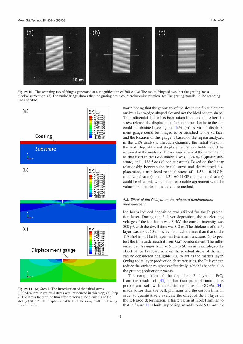
Finite element modeling of the slitting method was performed with the commercial software Simulia Abaqus. Since the slot length is much larger than the slot width or depth, a 2D elas-ticity analysis was performed with the plane strain model. A 2D mesh with CPE4R finite elements was suitable for the computation and the element density was large enough for sufficient computing accuracy. The modeling process can be mainly divided into two steps. The first step is to bring com-pressive/tensile residual stress to the elements. In the analysis, an initial stress of 100 MPa was first introduced into the film (see figure 11(a)). The second step is to remove the element corresponding to the geometry of the microslot. It is also
Figure 7. Curvature of the quartz wafer measured after the deposition of TiAlSiN film. (a) The TiAlSiN film with a quartz substrate. (b) The TiAlSiN film with a silicon substrate.
Figure 8. Schematic diagram of the milling process. Gratings A and B are both 20 μm × 20 μm and the slot is set to be milled between these two gratings.
Figure 9. (a) SEM image of the gratings after the milling step. (b) The magnification was increased to 12 000 × to capture the domain in the red dotted dashed line, and the region in the yellow dotted box is cropped for calculation. (c) The cross-section of the trench after the ion milling.
Meas. Sci. Technol. 25 (2014) 095003
R Zhu et al
8
worth noting that the geometry of the slot in the finite element analysis is a wedge-shaped slot and not the ideal square shape. This influential factor has been taken into account. After the stress release, the displacement/strain perpendicular to the slot could be obtained (see figure 11(b), (c)). A virtual displace-ment gauge could be imaged to be attached to the surface, and the location of this gauge is based on the region analyzed in the GPA analysis. Through changing the initial stress in the first step, different displacement/strain fields could be acquired in the analysis. The average strain of the same region as that used in the GPA analysis was −324.6 με (quartz sub-strate) and −188.5 με (silicon substrate). Based on the linear relationship between the initial stress and the released dis-placement, a true local residual stress of −1.58 ± 0.14 GPa (quartz substrate) and −1.31 ±0.11 GPa (silicon substrate) could be obtained, which is in reasonable agreement with the values obtained from the curvature method.
4.3. Effect of the Pt layer on the released displacement measurement
Ion beam-induced deposition was utilized for the Pt protec-tion layer. During the Pt layer deposition, the accelerating voltage of the ion beam was 30 kV, the current intensity was 500 pA with the dwell time was 0.2 μs. The thickness of the Pt layer was about 50 nm, which is much thinner than that of the TiAlSiN film. The Pt layer has two main functions: (i) to pro-tect the film underneath it from Ga+ bombardment. The influ-enced depth ranges from ~15 nm to 50 nm in principle, so the effect of ion bombardment on the residual stress of the film can be considered negligible. (ii) to act as the marker layer. Owing to its layer production characteristics, the Pt layer can reduce the surface roughness effectively, which is beneficial to the grating production process.
The composition of the deposited Pt layer is PtC8 from the results of [33], rather than pure platinum. It is porous and soft with an elastic modulus of ~8 GPa [34], much softer than the bulk platinum and the carbon film. In order to quantitatively evaluate the effect of the Pt layer on the released deformation, a finite element model similar to that in figure 11 is built, supposing an additional 50 nm-thick
Figure 10. The scanning moiré fringes generated at a magnification of 300 × . (a) The moiré fringe shows that the grating has a clockwise rotation. (b) The moiré fringe shows that the grating has a counterclockwise rotation. (c) The grating parallel to the scanning lines of SEM.
Figure 11. (a) Step 1: The introduction of the initial stress (100 MPa tensile residual stress was introduced in this step) (b) Step 2: The stress field of the film after removing the elements of the slot. (c) Step 2: The displacement field of the sample after releasing the constraint.
Meas. Sci. Technol. 25 (2014) 095003

R Zhu et al
9
Figure 12. (a) The 3 D displacement of the gratings along the x axis. (b) The averaged experimental ux displacements normal to the slot obtained from GPA. (Test 1 and test 2 are conducted on the film with quartz substrate. The calculated residual stresses are −1.48 GPa and −1.68 GPa, respectively. Test 3 and test 4 are conducted on the film with silicon substrate. The residual stresses calculated in the tests are −1.23 GPa and −1.38 GPa, respectively.)
Meas. Sci. Technol. 25 (2014) 095003

R Zhu et al
10
Pt layer is entirely tied to the film, and only elastic deforma-tion occurs after the residual stress release. Comparing the released displacement field of the model with and without the Pt layer, the former estimates the displacement with a discrepancy of less than 1%, which can be considered negli-gible in the present case.
5. Conclusion
In this study, a method combining FIB slot milling and GPA calculation was developed for the residual stress measurement of the micro-area under the FIB/SEM dual beam system. Taking advantage of sensor fabrication and high-resolution observation, the whole procedure of this method could be realized in one system. The residual stresses of TiAlSiN films were measured using this method, and the experimental results show good agreements with those obtained by the cur-vature method.
From our analysis, the possible influence factors of the operation process on stress assessment are considered. Due to the low elastic modulus and small thickness of the deposited Pt layer compared with the substrate and film, the influence is negligible in the present case according to analysis results from the finite element method simulation. Furthermore, the Ga+ bombardment may cause significant deterioration on the local image pattern, so it is necessary to decrease the exposure time in the FIB system with a lower beam current value.
Acknowledgment
The authors express their gratitude to Dr Shujun Zhou and Dr Xing Su for their great support with the sample prepa-ration. The authors are grateful for the financial support from the National Basic Research Program of China (‘973’ Project) (Grant Nos. 2010CB631005 and 2011CB606105), the National Natural Science Foundation of China (Grant Nos. 11232008, 91216301, 11227801 and 11172151), and the Tsinghua University Initiative Scientific Research Program.
References
[1] Ma C H, Huang J H and Chen H 2002 Residual stress measurement in textured thin film by grazing-incidence X-ray diffraction Thin Solid Films 418 73–8
[2] Albertini G et al 1999 Determination of residual stresses in materials and industrial components by neutron diffraction Meas. Sci. Technol. 10 R56–73
[3] Choi H C and Park J H 2005 Prediction of residual stress distribution in multi-stacked thin film by curvature measurement and iterative FEA J. Mech. Sci Technol. 19 1065–71
[4] He Q, Luo Z X and Chen X Y 2008 Comparison of residual stress measurement in thin films using surface micromachining method Thin Solid Films 516 5318–23
[5] Zhou Z M et al 2004 The evaluation of Young’s modulus and residual stress of nickel films by microbridge testings Meas. Sci. Technol. 15 2389–94
[6] Zhou Z et al 2007 Residual strain of a Cr film characterized by micromachined beams Meas. Sci. Technol. 18 3399
[7] Xie H et al 2003 Focused ion beam Moiré method Opt. Lasers Eng. 40 163–77
[8] Li B et al 2002 Investigation of strain in microstructures by a novel moiré method Microelectromech. Syst. J. 11 829–36
[9] Li B et al 2004 Strain analysis in MEMS/NEMS structures and devices by using focused ion beam system Sensors Actuators A 111 57–62
[10] Xie H et al 2004 Phase shifting SEM moiré method Opt. Laser Technol. 36 291–7
[11] Massl S, Keckes J and Pippan R 2007 A direct method of determining complex depth profiles of residual stresses in thin films on a nanoscale Acta Mater. 55 4835–44
[12] Kang K J et al 2003 A method for in situ measurement of the residual stress in thin films by using the focused ion beam Thin Solid Films 443 71–7
[13] Sabate N et al 2006 Digital image correlation of nanoscale deformation fields for local stress measurement in thin films Nanotechnology 17 5264–70
[14] Winiarski B and Withers P J 2012 Micron-scale residual stress measurement by micro-hole drilling and digital image correlation Exp. Mech. 52 417–28
[15] Winiarski B et al 2012 Submicron-scale depth profiling of residual stress in amorphous materials by incremental focused ion beam slotting Acta Mater. 60 2337–49
[16] Krottenthaler M et al 2012 A simple method for residual stress measurements in thin films by means of focused ion beam milling and digital image correlation Surf. Coat. Technol. 215 247–52
[17] Schajer G S, Winiarski B and Withers P J 2013 Hole-drilling residual stress measurement with artifact correction using full-field DIC Experimental and Applied Mechanics vol 4 (New York: Springer) pp 403–14
[18] Sebastiani M et al 2011 Depth-resolved residual stress analysis of thin coatings by a new FIB–DIC method Mater. Sci. Eng. A 528 7901–8
[19] Zhu R H et al 2014 A micro-scale strain rosette for residual stress measurement by SEM Moiré method Sci. China Phys. Mech. Astron. 57 716–22
[20] Takeda M and Suzuki J 1996 Crystallographic heterodyne phase detection for highly sensitive lattice-distortion measurements J. Opt. Soc. Am. A 13 1495–500
[21] Hÿtch M J, Putaux J L and Pénisson J M 2003 Measurement of the displacement field of dislocations to 0.03 Å by electron microscopy Nature 423 270–73
[22] Wu D et al 2014 A novel method to fabricate micro-gratings applied for deformation measurement around a crack in a thin film Meas. Sci. Technol. 25 025012
[23] Liu Z W et al 2009 The digital geometric phase technique applied to the deformation evaluation of MEMS devices J. Micromech. Microeng. 19 015012
[24] Liu Z W et al 2013 GPA combined with the hole drilling method applied for curved surface strain measurement Strain 49 46–53
[25] Wang Q et al 2012 In situ high temperature creep deformation of micro-structure with metal film wire on flexible membrane using geometric phase analysis Microelectron. Reliab. 53 652–7
[26] Wang Q et al 2010 Residual stress assessment of interconnects by slot milling with FIB and geometric phase analysis Opt. Lasers Eng. 48 1113–8
[27] Rouviere J L and Sarigiannidou E 2005 Theoretical discussions on the geometrical phase analysis Ultramicroscopy 106 1–17
[28] Zhao B and Asundi A 2000 Discussion on spatial resolution and sensitivity of Fourier transform fringe detection Opt. Eng. 39 2715–9
Meas. Sci. Technol. 25 (2014) 095003

R Zhu et al
11
[29] Takeda M, Ina H and Kobayashi S 1982 Fourier-transform method of fringe-pattern analysis for computer-based topography and interferometry J. Opt. Soc. Am. 72 156–60
[30] Doumalin P and Bornert M 2000 Micromechanical applications of digital image correlation techniques Interferometry in Speckle Light (Berlin: Springer) pp 67–74
[31] Pan B, Lu Z and Xie H 2010 Mean intensity gradient: an effective global parameter for quality assessment of the speckle patterns used in digital image correlation Opt. Lasers Eng. 48 469–77
[32] Stoney G G 1909 The tension of metallic films deposited by electrolysis Proc. R. Soc. Lond. A 82 172–5
[33] Van Kouwen L, Botman A and Hagen C W 2009 Focused electron-beam-induced deposition of 3 nm dots in a scanning electron microscope Nano Lett. 9 2149–52
[34] Song X et al 2012 Residual stress measurement in thin films at sub-micron scale using focused ion beam milling and imaging Thin Solid Films 520 2073–6
Meas. Sci. Technol. 25 (2014) 095003