MCT Based Photovoltiac Detectors
14
1 Mercury Cadmium Telluride (HgCdTe) based Photovoltaic Detectors Submitted by: Muhammad Shoaib and Malik M, Haris Amir, Submitted to: Dr Adnan Masood Department of Electrical Engineering, College of Electrical & Mechanical Engineering, National University of Sciences & Technology, Rawalpindi 1. Introduction There are several semiconductor devices that can be used to detect the presence of photons. These devices, known as photodetectors, are used to convert o ptical signals to electrical signals. When excess electrons and holes are generated in a semiconductor due to illumination by photons, the conductivity of the semiconductor material is increased. This principle is the basis of operation of photodetectors [1] . The main types of photodetectors are thermal and photonic detectors. The thermal effects of the incident radiation can be followed through many temperature dependent phenomena. Bolometers and micro bolometers are based on ch anges in resistance. Thermocouples and thermopiles use the thermoelectric effect. Golay c ells follow the rmal expansion. In IR, spectrometers the pyroelectric detectors are the most widespread. The response time and sensitivity of photonic detectors can be much higher, but usually these have to be cooled to cut thermal noise. The materials in these are semiconductors with narrow band gaps. Incident IR photons can cause electronic excitations. In photoconductive detectors, the resistivity of the detector element is monitored. Photovoltaic detectors contain a p-n junction on which photoelectric current appears upon illumination. HgCdTe [2] is a pseudo-binary alloy semiconductor that crystallizes in a zinc-blende structure. Because of its band gap tunalbility with Hg1− xCd xTe has evolved to become the most important/versatile material for detector applications over the entire IR range. As the Cd composition increases, the energy gap for Hg 1− xCd xTe gradually increases from a negative value
-
Upload
shoaib-muhammad -
Category
Documents
-
view
215 -
download
0
Transcript of MCT Based Photovoltiac Detectors

8/15/2019 MCT Based Photovoltiac Detectors
http://slidepdf.com/reader/full/mct-based-photovoltiac-detectors 1/14

8/15/2019 MCT Based Photovoltiac Detectors
http://slidepdf.com/reader/full/mct-based-photovoltiac-detectors 2/14
8/15/2019 MCT Based Photovoltiac Detectors
http://slidepdf.com/reader/full/mct-based-photovoltiac-detectors 3/14
3
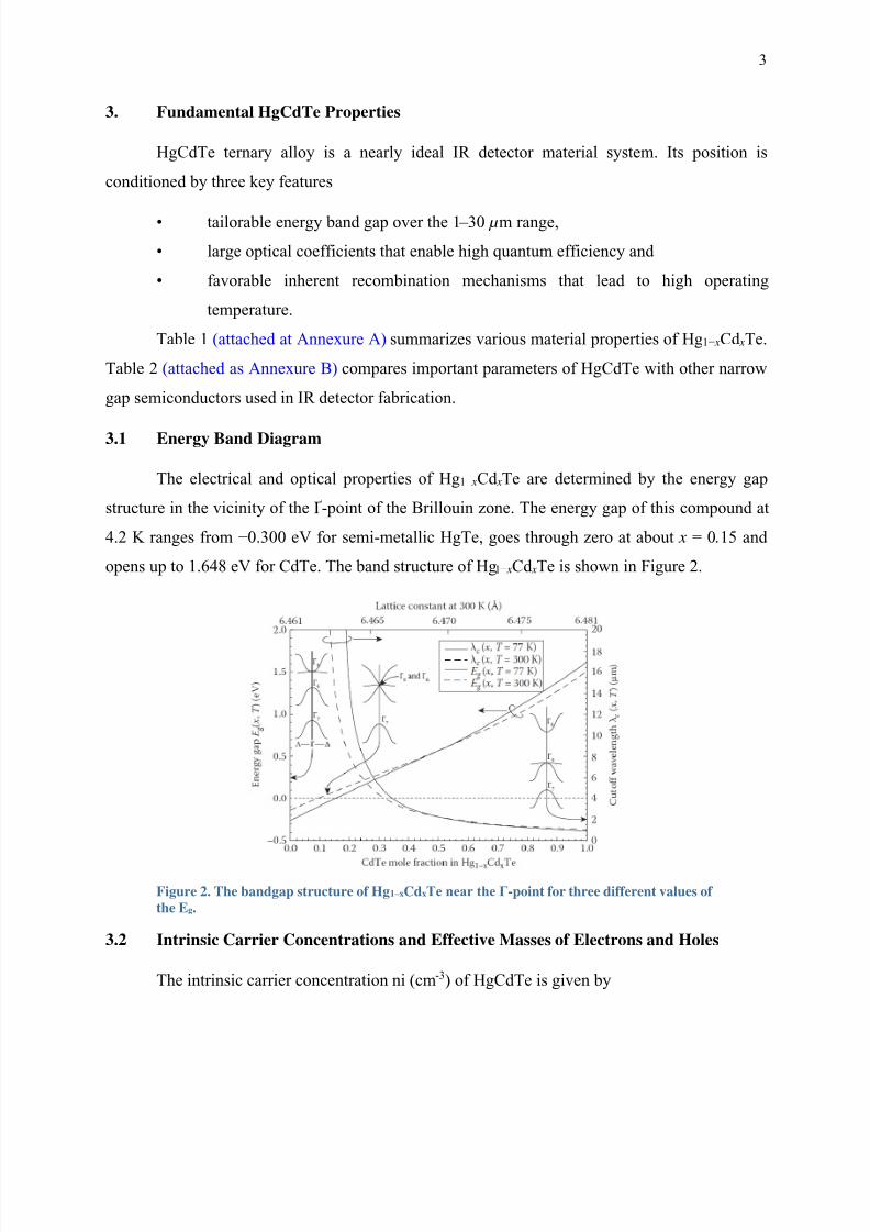
3. Fundamental HgCdTe Properties
HgCdTe ternary alloy is a nearly ideal IR detector material system. Its position is
conditioned by three key features
• tailorable energy band gap over the 1 – 30 µm range,
• large optical coefficients that enable high quantum efficiency and
• favorable inherent recombination mechanisms that lead to high operating
temperature.
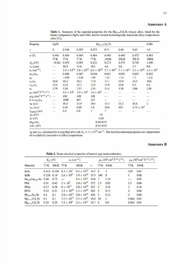
Table 1 (attached at Annexure A) summarizes various material properties of Hg1− xCd xTe.
Table 2 (attached as Annexure B) compares important parameters of HgCdTe with other narrow
gap semiconductors used in IR detector fabrication.
3.1 Energy Band Diagram
The electrical and optical properties of Hg1− xCd xTe are determined by the energy gap
structure in the vicinity of the Ґ-point of the Brillouin zone. The energy gap of this compound at
4.2 K ranges from −0.300 eV for semi-metallic HgTe, goes through zero at about x = 0.15 and
opens up to 1.648 eV for CdTe. The band structure of Hg1− xCd xTe is shown in Figure 2.
Figure 2. The bandgap structure of Hg1 – xCdxTe near the Γ-point for three different values of
the Eg.
3.2 Intrinsic Carrier Concentrations and Effective Masses of Electrons and Holes
The intrinsic carrier concentration ni (cm-3) of HgCdTe is given by

8/15/2019 MCT Based Photovoltiac Detectors
http://slidepdf.com/reader/full/mct-based-photovoltiac-detectors 4/14

8/15/2019 MCT Based Photovoltiac Detectors
http://slidepdf.com/reader/full/mct-based-photovoltiac-detectors 5/14
5
3.5 Optical Properties
Optical absorption coefficient data for several alloy compositions of Hg1− xCd xTe versus
wavelength are plotted in Figure 3. We can see that the absorption strength generally decreases
as the gap becomes smaller.
Figure 3. Optical absorption coefficient plotted versus wavelength
3.6 Lattice Constants
The use of CdTe for passivation is very promising since it has high resistivity, is lattice
matched, and is chemically compatible to Hg1−xCd xTe. Barriers can be found in both the
conduction and valence band. The comparison of lattice constants of various materials is shown
in Figure 4.
Figure 4. Comparison of lattice constants of various semiconductors vs bandgap energy and
wavelength

8/15/2019 MCT Based Photovoltiac Detectors
http://slidepdf.com/reader/full/mct-based-photovoltiac-detectors 6/14
6
3.7 Generation – Recombination Processes
The generation processes which compete against the recombination processes directly affect
the performance of photodetectors, setting up a steady-state concentration of carriers in
semiconductors subjected to thermal and optical excitation and, frequently determining thekinetics of photo generated signals.
3.7.1 Radiative Processes
In HgCdTe, the internal radiative processes although of fundamental nature, do not limit the
ultimate performance of IR detectors.
3.7.2 Auger Processes
Auger mechanisms dominate generation and recombination processes in Hg1−xCd xTe at near
room temperatures. The Auger generation and recombination rates are strongly dependent on
temperature via dependence of carrier concentration and intrinsic time on temperature.
Therefore, cooling is a natural and a very effective way to suppress Auger processes.
3.7.3 Carrier Lifetimes
The total carrier lifetime τ total can be calculated from the independent lifetimes attributed to
each recombination mechanism. The sum of all contributions is given by
4. Operation of HgCdTe p-n Junction Photodiode[4]
The photovoltaic p-n junction photodiode is representative of high performance HgCdTe
IR detector technology. Figure 5 illustrates the basic operation of a simple p-n homojunction
detector under illuminated zero-bias and reverse bias conditions. Incident photons with energy
greater than the material bandgap (E ph>Eg) generate electron-hole pairs in the material on either
side of the p-n junction.
Carriers generated within a diffusion length of the space-charge region diffuse to the
electrical junction and are separated by the strong electric field. The electron and hole minority
carrier diffusion lengths Ln and L p (cm) are given by
(Eq. 4)

8/15/2019 MCT Based Photovoltiac Detectors
http://slidepdf.com/reader/full/mct-based-photovoltiac-detectors 7/14
7
where τ n and τ p are the electron and hole minority carrier recombination lifetimes(s), and Dn and
D p are the electron and hole minority carrier diffusion coefficients (cm2s-1).
Figure 5. Schematic of structure and energy band diagram of a HgCdTe p-n homo-junction
photodetector device at zero-bias (inset) and under reverse bias and illumination.
Figure 6. Schematic representation of current-voltage characteristics of photodiode
The optically excited minority carriers that are injected into the opposite side of the
junction by the E field become majority carriers. By this process, a photocurrent density J ph is
generated by the incident radiation, increasing the dark saturation current value as illustrated in
Figure 6.
The total current density J total (A/cm2) in the p-n junction photodiode is given by[3]
(Eq. 5)

8/15/2019 MCT Based Photovoltiac Detectors
http://slidepdf.com/reader/full/mct-based-photovoltiac-detectors 8/14
8
J total(V bias) = J dark (V bias) -J ph(φ) (Eq.6)
where J dark depends on V bias, and J ph depends on the incident photon flux density (ph/cm2s). In a
simple photovoltaic detector with no gain, the photocurrent is equivalent to[3]
I ph = J ph A = nqφ A (Eq. 7)
4.1 Detector Structure
Most commonly used photovoltaic HgCdTe photodiodes are fabricated in a homojunction
configuration with a highly doped n+ cap layer in contact with a lightly doped, narrow bandgap
p-type absorber (base) layer, or in a heterojunction configuration with wide bandgap (denoted by
capitalized letter) P+ cap layer in contact with a lightly doped, narrow bandgap n-type absorber
layer, as shown in Figure 7.
In these structures, the absorber layer determines the dark current and photo current of
the device. The base layer doping in both structures must be below1016 cm-3 to avoid tunneling
current contribution, and the doping
Figure 7. Schematic of energy band diagrams of commonly used unbiased (a) n-on-p
homojunction and (b) P-on-n heterojunction photodiodes under backside illumination
values used are typically ~5×1015 cm-3 and ~5×1014 cm-3 for p-type and n-type layers,
respectively.

8/15/2019 MCT Based Photovoltiac Detectors
http://slidepdf.com/reader/full/mct-based-photovoltiac-detectors 9/14
9
Figure 8. HgCdTe DLHJ structure on Si substrate for FPA integration
Double layer heterojunction (DLHJ) architectures, shown in Figure 8, have been
developed for high performance LWIR detectors due to low thermal leakage currents[5].
4.2 Current Contribution Mechanisms
The diffusion current I diff (A) is described by the basic diode equation,
and n po and pno are the equilibrium electron and hole concentrations (cm-3) on the p- and n-sides
of the junction, respectively. These mechanisms, several of which are illustrated in Figure 9,
include generation-recombination (G-R) in the depletion region, band-to-band (BTB) tunneling,
trap-assisted tunneling (TAT), and surface recombination. The total dark current can be
expressed as the sum of all contributions
Materials with narrow bandgaps are especially susceptible to thermal G-R processes that
dominate the dark current at high temperatures. The dark current contribution to overall current
is illustrated in Figure 10.
where

8/15/2019 MCT Based Photovoltiac Detectors
http://slidepdf.com/reader/full/mct-based-photovoltiac-detectors 10/14
10
Figure 9. Schematic of structure and energy band diagram of a HgCdTep-n junction DLPH
photodetector device under reverse bias and illumination.
Figure 10 - Dark current contribution mechanisms in reverse-biased p-n junction
Band-to-band tunneling occurs when electrons at a given energy level tunnel across the
bandgap from the valence band on one side of a junction to the conduction band on the other to
fill an unoccupied state at the same energy level. Band-to-band tunneling exhibits a strong
dependence on E g and E field , where the field strength depends on V bias and the doping
concentration of the junction. Trap assisted tunneling is caused by carriers tunneling within the
depletion region via intermediate trap states created by impurities or defects. The tunneling
occurs in a two-step process involving one thermal transition from the valence band to the trap
state and a second transition from the trap state to the conduction band. Because the required
transition energies are smaller, trap-assisted tunneling occurs at lower fields than band-to-band
8/15/2019 MCT Based Photovoltiac Detectors
http://slidepdf.com/reader/full/mct-based-photovoltiac-detectors 11/14

8/15/2019 MCT Based Photovoltiac Detectors
http://slidepdf.com/reader/full/mct-based-photovoltiac-detectors 12/14
12
extremely small change of lattice constant with composition makes it possible to grow high
quality layers and heterostructures. HgCdTe can be used for detectors operated at various modes,
and can be optimized for operation at the extremely wide range of the IR spectrum (1 – 30 µm)
and at temperatures ranging from that of liquid helium to room temperature.
7. Limitations of HgCdTe Detectors
Thermal G-R processes, namely intrinsic Auger generation, dominate the dark current
density in narrow bandgap materials, fundamentally limiting the detector performance at higher
temperatures. Thus, high performance detectors are typically operated at cryogenic temperatures
(77 K or lower). These cooling systems are extremely bulky, require high input power, and are
prohibitively costly to implement. Increasing the detector operating temperature to a range where
the cooling requirements can be met by TE coolers (193 K-253 K) is advantageous as thesesystems are smaller, simpler, and less expensive to integrate
At the processing level, achieving stable, well-controlled, extrinsic p-type doping
required for p-n junction PV structures by ex situ ion implantation or in situ doping via molecular
beam epitaxy (MBE) poses a significant challenge for HgCdTe detector technology. Ex situ
doping techniques (implantation, in-diffusion) cannot easily provide the level of control over
doping profiles necessary for abrupt junction, multi-layer structures and can introduce material
damage, reducing the carrier mobilities and minority carrier lifetimes.
8. Conclusion
HgCdTe is an important material for high performance IR photodetectors and continues
to outperform competing materials, achieving near theoretical performance limits. Properties
such as the high absorption coefficient, high carrier mobility, and lattice matched bandgap
tunability make HgCdTe an attractive option for IR detector applications. However, extrinsic and
intrinsic G-R processes such as SRH, radiative, and Auger mechanisms are major factors which
affect detector performance in narrow bandgap materials and must be taken into account.
8/15/2019 MCT Based Photovoltiac Detectors
http://slidepdf.com/reader/full/mct-based-photovoltiac-detectors 13/14

8/15/2019 MCT Based Photovoltiac Detectors
http://slidepdf.com/reader/full/mct-based-photovoltiac-detectors 14/14
14
References
[1]Donald A. Neaman “ Semiconductor Physics and Devices” 3 rd Edition, 2003, McGrawHill,
ISBN 0-07-232107-5
[2]Antoni Rogalski, “HgCdTe Infrared Detector Material: History, Status And Outlook”, Reports
on Progress in Physics, Pages from 2269 to 2331, Rep. Prog. Phys. 68 (2005) 2267 – 2336,
Published 22 August 2005, Institute Of Physics Publishing.
[3][Online] Available at https://en.wikipedia.org/wiki/Infrared_detector.
[4]Anne M. Itsuno, “Bandgap-Engineered HgCdTe Infrared DetectorStructures for Reduced
Cooling Requirements”, 2012, The University of Michigan
[5]P. Capper and J. Garland, editors. Mercury Cadmium Telluride, Growth, Properties and
Applications. Wiley, 2011.
[6] Antoni Rogalski, “Infrared Detectors”, 2nd Edition, CRC Press, ISBN 978-1-4200-7671-4