MCS9922 PCIe to Dual Serial Controller Datasheet · An I2C interface is provided to configure...
38
1 MCS9922 PCIe to Dual Serial Controller Copyright © 2010-2011 ASIX Electronics Corporation. All rights reserved. Revision 2.00 Aug. 5 th , 2011 MCS9922 PCIe to Dual Serial Controller Datasheet
Transcript of MCS9922 PCIe to Dual Serial Controller Datasheet · An I2C interface is provided to configure...

1
MCS9922PCIe to Dual Serial Controller
Copyright © 2010-2011 ASIX Electronics Corporation. All rights reserved.
Revision 2.00Aug. 5th, 2011
MCS9922 PCIe to Dual Serial Controller
Datasheet

2
MCS9922PCIe to Dual Serial Controller
Copyright © 2010-2011 ASIX Electronics Corporation. All rights reserved.
IMPORTANT NOTICE Copyright © 2010-2011 ASIX Electronics Corporation. All rights reserved. DISCLAIMER No part of this document may be reproduced or transmitted in any form or by any means, electronic or mechanical, including photocopying and recording, for any purpose, without the express written permission of ASIX. ASIX may make changes to the product specifications and descriptions in this document at any time, without notice. ASIX provides this document “as is” without warranty of any kind, either expressed or implied, including without limitation warranties of merchantability, fitness for a particular purpose, and non-infringement. Designers must not rely on the absence or characteristics of any features or registers marked “reserved”, “undefined” or “NC”. ASIX reserves these for future definition and shall have no responsibility whatsoever for conflicts or incompatibilities arising from future changes to them. Always contact ASIX to get the latest document before starting a design of ASIX products. TRADEMARKS ASIX, the ASIX logo are registered trademarks of ASIX Electronics Corporation. All other trademarks are the property of their respective owners.

3
MCS9922PCIe to Dual Serial Controller
Copyright © 2010-2011 ASIX Electronics Corporation. All rights reserved.
Table of Contents 1 Introduction .............................................................................................................................. 4
1.1 Block Diagram ............................................................................................................................... 4 1.2 Features ........................................................................................................................................ 5 1.3 Applications .................................................................................................................................. 6 1.4 Ordering information .................................................................................................................... 6 1.5 Support ......................................................................................................................................... 6
2 Pin Diagram ............................................................................................................................... 7 2.1 MCS9922CV‐AA Pin diagram ........................................................................................................ 7
3 Pin Description .......................................................................................................................... 8 3.1 Pin configurations ......................................................................................................................... 8 3.2 PCI Express Interface Signals ........................................................................................................ 9 3.3 Serial Port Interface Signals ........................................................................................................ 10 3.4 Cascade Interface Signals ........................................................................................................... 11 3.5 I2C Interface Signals .................................................................................................................... 12 3.6 GPIO Interface Signals ................................................................................................................ 12 3.7 Clock/Crystal Oscillator Interface Signals ................................................................................... 13 3.8 Test Mode Signals ....................................................................................................................... 13 3.9 JTAG Interface Signals ................................................................................................................. 13 3.10 Power Supply Signals .................................................................................................................. 14
4 Function Mapping ................................................................................................................... 16 5 Functional Description ............................................................................................................ 17
5.1 PCIe Operation ............................................................................................................................ 17 5.2 PCIe Configuration Space ........................................................................................................... 19 5.3 Serial Port ................................................................................................................................... 22 5.4 I2C ................................................................................................................................................ 24 5.5 PM Control .................................................................................................................................. 25 5.6 Cascade Interface ....................................................................................................................... 26 5.7 Clocks and Resets ....................................................................................................................... 29 5.8 GPIO ............................................................................................................................................ 30
6 EEPROM Contents Layout ....................................................................................................... 31 7 Electrical Specifications ........................................................................................................... 34 8 Mechanical Dimensions .......................................................................................................... 36 Revision History ............................................................................................................................ 37

4
MCS9922PCIe to Dual Serial Controller
Copyright © 2010-2011 ASIX Electronics Corporation. All rights reserved.
1 Introduction MCS9922 is a single lane multifunction PCI express to I/O controller. It supports two serial ports and eight GPIO’s. MCS9922 also provides an option for peripheral expansion through ASIX proprietary Cascade interface. The generic cascade interface allows interconnecting with similar chips like MCS9900 to expand the peripheral ports. The serial ports are compatible with RS232, RS422 & RS485 standards and supports throughput from 50bps to 16Mbps. All the GPIO pins are programmable and can be used as Input or Output. An I2C interface is provided to configure MCS9922 device options through an external EEPROM.
1.1 Block Diagram

5
MCS9922PCIe to Dual Serial Controller
Copyright © 2010-2011 ASIX Electronics Corporation. All rights reserved.
1.2 Features PCI express • Single‐lane (X1) PCI Express End‐point Controller with integrated PHY • Compliant with PCI Express Base Specification, Revision 1.1 • Compliant with PCI Express card specifications • Supports two PCI Express functions • Supports auto completion of configuration requests • Supports built in flow control • Supports Message TLP (Error) generation • Supports integrated time out handling of Non‐posted request • Supports both legacy and MSI Interrupt • Supports PCIe Power Management
Serial Port • Two 16C450 / 550 / Extended 550 / 650 / ASIX Enhanced Mode compatible UARTs • Supports RS232, RS422 & RS485 modes • Bi‐directional speeds from 50 bps to 16 Mbps per port • Full Serial Modem Control • Supports Hardware, Software Flow Control • Supports 5, 6, 7, 8 bit Serial format • Supports Even, Odd, None, Space and Mark parity • Supports Custom baud rate by programming internal PLL or external clock • Supports On Chip 256 Byte depth FIFOs in Transmit, Receive path of each Serial Port • Supports remote wakeup and power management features • Serial Port transceiver shutdown support • Supports Slow IrDA mode (up to 115200bps) on all Serial Ports
Cascade MCS9922 supports a 13‐Pin proprietary interface to connect to other ASIX devices for IO expansion. Through this interface, MCS9922 can be used as Cascade Secondary device and can be connected to Cascade Primary capable ASIX Devices like MCS9900.
Eg. MCS9922 can be connected to MCS9900, for following product configurations.
• PCIe to 6 Serial Ports • PCIe to 4 Serial Ports and 1 Parallel Port

6
MCS9922PCIe to Dual Serial Controller
Copyright © 2010-2011 ASIX Electronics Corporation. All rights reserved.
General Device Features • I2C interface for EEPROM • EEPROM read / write through PCIe Interface • 8 bi‐directional multi‐function GPIO lines • On chip oscillator • Power supply : 1.2V, 3.3V
1.3 Applications • Serial Attached Devices • Serial Networking / Monitoring Equipment • Data Acquisition System • POS Terminal & Industrial PC • Add‐On I/O Cards – Serial • Embedded systems – For I/O expansion
1.4 Ordering information • Ordering Part Number : MCS9922CV‐AA • Operating Temperature : 0 to 85 deg C • Package : 128 LQFP, RoHS
1.5 Support • Reference Schematics : Available *** • Evaluation Board : Available *** • Software Support : Available *** • System Design Data & Other Technical Collateral : Available ***
*** Please contact ASIX Support Team for above items, write to [email protected]

7
MCS9922PCIe to Dual Serial Controller
Copyright © 2010-2011 ASIX Electronics Corporation. All rights reserved.
2 Pin Diagram
2.1 MCS9922CV‐AA Pin diagram

8
MCS9922PCIe to Dual Serial Controller
Copyright © 2010-2011 ASIX Electronics Corporation. All rights reserved.
3 Pin Description Pin Naming Convention The Pin names use the following conventions: “n” suffix is an active low signal, “I” – Input, “O” – Output, “P” – Passive, “DS” – Drive Strength in milli Amperes(mA), “PU” – Pull Up, “PD” – Pull Down, “N/A” – Not Applicable and “PROG” – Programmable
3.1 Pin configurations Following table describes the pin configurations of MCS9922CV‐AA device. Pin MCS9922 Pin MCS9922 Pin MCS9922 Pin MCS9922 1 REFCLK_M 37 NC 73 SCAN_MODE 109 VCC3IO 2 REFCLK_P 38 NC 74 TCK 110 CASC_REQ3 VCC12A_AUX 39 NC 75 TDI 111 CASC_ACK4 REXT 40 NC 76 TDO 112 CASC_VAL5 GND12A 41 NC 77 TMS 113 CASC_AD[0]6 RXDN 42 GND3IO 78 TRST_n 114 CASC_AD[1]7 RXDP 43 VCC3IO 79 I2C_SCL 115 CASC_AD[2]8 GND12A 44 GNDK 80 I2C_SDA 116 CASC_AD[3]9 VCC12A 45 VCCK 81 GPIO_0 117 CASC_AD[4]10 TXDP 46 NC 82 GPIO_1 118 CASC_AD[5]11 TXDN 47 NC 83 GPIO_2 119 CASC_AD[6]12 VCC12A 48 NC 84 GPIO_3 120 GND3IO13 VCC33A_PLL 49 NC 85 GPIO_4 121 VCC3IO 14 GND33A_PLL 50 NC 86 GPIO_5 122 CASC_AD[7]15 GND33A_AUX 51 NC 87 GND3IO 123 CASC_GNT16 VCC33A_AUX 52 NC 88 NC 124 CASC_EN17 VCC12A_PLL 53 NC 89 VCC3IO 125 CASC_PRIM18 GND12A_PLL 54 GPIO_6 90 VCC33A_LVDS 126 SEC_DEV_MODE19 VCCK 55 GPIO_7 91 GND33A_LVDS 127 SEC_DEV_ID20 GNDK 56 SP1_TX 92 VCC33D_DLL 128 CASC_CLK21 WAKE_n 57 SP1_DTR_n 93 GND33A_DLL 22 CLK_SEL 58 SP1_RTS_n 94 NC 23 GND3IO 59 SP1_RX 95 NC 24 VCC3IO 60 SP1_RI_n 96 NC 25 PCIe_RST_n 61 SP1_DSR_n 97 NC 26 SP2_TX 62 SP1_DCD_n 98 VCC12A_PLL 27 SP2_DTR_n 63 SP1_CTS_n 99 GND12A_PLL 28 SP2_RTS_n 64 NC 100 VCCK 29 SP2_RX 65 NC 101 GNDK 30 SP2_RI_n 66 GND3IO 102 VCC3IO 31 SP2_DSR_n 67 VCC3IO 103 XTAL_I 32 SP2_DCD_n 68 NC 104 XTAL_IO 33 SP2_CTS_n 69 NC 105 GND3IO 34 NC 70 VCCK 106 GND3IO 35 NC 71 GNDK 107 VCC3IO 36 NC 72 SCAN_EN 108 GND3IO

9
MCS9922PCIe to Dual Serial Controller
Copyright © 2010-2011 ASIX Electronics Corporation. All rights reserved.
3.2 PCI Express Interface Signals Pin# Pin Name I/O/P Type DS PU/PD Description
1 REFCLK_M I LVDS – –
PCIe PHY differential PLL reference clock. Cascade Mode: Pull down using 10K Resistor.
2 REFCLK_P I LVDS – –
PCIe PHY differential PLL reference clock. Cascade Mode: Pull down using 10K Resistor.
4 REXT O Analog – –
Bandgap External Resistor (Connect this pin to ground through an external resistor of 6.2KΩ, ±1%)
6 RXDN I LVDS – –
PCIe PHY differential negative serial data input. Cascade Mode: Pull down using 10K Resistor.
7 RXDP I LVDS – –
PCIe PHY differential positive serial data input. Cascade Mode: Pull down using 10K Resistor.
10 TXDP O LVDS – –
PCIe PHY differential positive serial data output. Cascade Mode: Leave this pin as “No Connection”.
11 TXDN O LVDS – –
PCIe PHY differential negative serial data output. Cascade Mode: Leave this pin as “No Connection”.
21 WAKE_n O LVTTL 4 PU
This is an active low signal used to reactivate the PCI Express slot’s main power and reference clocks. Cascade Mode: Leave this pin as “No Connection”.
22 CLK_SEL O LVTTL 4 PU Used to enable/disable clock of PCI Express card.
25 PCIe_RST_n I LVTTL 4 PU Active low asynchronous reset from PCIe RC

10
MCS9922PCIe to Dual Serial Controller
Copyright © 2010-2011 ASIX Electronics Corporation. All rights reserved.
3.3 Serial Port Interface Signals Serial Port 1
Pin# Pin name I/O/P Type DS PU/PD Description
56 SP1_TX O LVTTL 4 – Transmit data out to transceiver or IrDA data out to IR LED
57 SP1_DTR_n O LVTTL 4 –
Data terminal ready (Active Low) Also used for setting cascade clock Pull up : Sets cascade clock to run at 62.5 MHz Pull down : Sets cascade clock to run at 96 MHz
58 SP1_RTS_n O LVTTL 4 – Request to send (Active Low)
59 SP1_RX I LVTTL 4 PU Serial receives data in from transceiver or IrDA data in from IrDA detector.
60 SP1_RI_n I LVTTL 4 PU Ring Indicator (Active Low)
61 SP1_DSR_n I LVTTL 4 PU Data Set Ready (Active Low)
62 SP1_DCD_n I LVTTL 4 PU Data Carrier Detect (Active Low)
63 SP1_CTS_n I LVTTL 4 PU Clear to send (Active Low)
Serial Port 2
Pin# Pin name I/O/P Type DS PU/PD Description
26 SP2_TX O LVTTL 4 – Transmit data out to transceiver or IrDA data out to IR LED
27 SP2_DTR_n O LVTTL 4 – Data terminal ready (Active Low)
28 SP2_RTS_n O LVTTL 4 – Request to send (Active Low)
29 SP2_RX I LVTTL 4 PU Serial receives data in from transceiver or IrDA data in from IrDA detector.
30 SP2_RI_n I LVTTL 4 PU Ring Indicator (Active Low) 31 SP2_DSR_n I LVTTL 4 PU Data Set Ready (Active Low) 32 SP2_DCD_n I LVTTL 4 PU Data Carrier Detect (Active Low) 33 SP2_CTS_n I LVTTL 4 PU Clear to send (Active Low)

11
MCS9922PCIe to Dual Serial Controller
Copyright © 2010-2011 ASIX Electronics Corporation. All rights reserved.
3.4 Cascade Interface Signals Pin# Pin name I/O/P Type DS PU/PD Description
110 CASC_REQ I/O LVTTL 8 – To request the arbiter to grant access to CASC_AD bus.
111 CASC_ACK I/O LVTTL 8 –
Asserted by slave, in response to CASC_VAL, when it is ready to accept transfer
112 CASC_VAL I/O LVTTL 8 – 1: address/data/command on CASC_AD[7:0] is valid, 0: CASC_AD is not valid
113 CASC_AD[0] I/O LVTTL 8 – To transfer Address / Data and control words
114 CASC_AD[1] I/O LVTTL 8 – To transfer Address / Data and control words
115 CASC_AD[2] I/O LVTTL 8 – To transfer Address / Data and control words
116 CASC_AD[3] I/O LVTTL 8 – To transfer Address / Data and control words
117 CASC_AD[4] I/O LVTTL 8 – To transfer Address / Data and control words
118 CASC_AD[5] I/O LVTTL 8 – To transfer Address / Data and control words
119 CASC_AD[6] I/O LVTTL 8 – To transfer Address / Data and control words
122 CASC_AD[7] I/O LVTTL 8 – To transfer Address / Data and control words
123 CASC_GNT I/O LVTTL 8 – Grant to access of CASC_AD bus
124 CASC_EN I LVTTL 4 PD 1 : cascade mode enabled 0 : cascade mode disabled
125 CASC_PRIM I LVTTL 4 PD Chip is cascade secondary. Leave this pin as “No Connection”.

12
MCS9922PCIe to Dual Serial Controller
Copyright © 2010-2011 ASIX Electronics Corporation. All rights reserved.
126 SEC_DEV_MODE O LVTTL 8 PD
For Non‐Cascade applications, leave this pin as No Connect. When MCS9922 is used as Cascade Secondary Device, connect this pin to corresponding pin of the Cascade Primary Device.
127 SEC_DEV_ID I LVTTL 4 PD Leave this pin as “No Connection”
128 CASC_CLK O LVTTL 8 Pull down using 1K resistor
3.5 I2C Interface Signals Pin# Pin name I/O/P Type DS PU/PD Description 79 I2C_SCL I/O LVTTL 4 PU 2‐Wire EEPROM Clock 80 I2C_SDA I/O LVTTL 4 PU 2‐Wire EEPROM Data in/out.
3.6 GPIO Interface Signals Pin# Pin name I/O/P Type DS PU/PD Description 81 GPIO_0 I/O LVTTL 8 PU/PD General Purpose I/O signal 82 GPIO_1 I/O LVTTL 8 PU/PD General Purpose I/O signal 83 GPIO_2 I/O LVTTL 8 PU/PD General Purpose I/O signal 84 GPIO_3 I/O LVTTL 8 PU/PD General Purpose I/O signal 85 GPIO_4 I/O LVTTL 8 PU/PD General Purpose I/O signal 86 GPIO_5 I/O LVTTL 8 PU/PD General Purpose I/O signal 54 GPIO_6 I/O LVTTL 8 PU/PD General Purpose I/O signal 55 GPIO_7 I/O LVTTL 8 PU/PD General Purpose I/O signal

13
MCS9922PCIe to Dual Serial Controller
Copyright © 2010-2011 ASIX Electronics Corporation. All rights reserved.
3.7 Clock/Crystal Oscillator Interface Signals Pin# Pin name I/O/P Type DS PU/PD Description 103 XTAL_I I Analog – – Crystal input for PLL, 24 ~ 42MHz
104 XTAL_IO I/O Analog – – Feedback signal for the oscillator pad
3.8 Test Mode Signals Pin# Pin name I/O/P Type DS PU/PD Description 72 SCAN_EN I LVTTL 4 PD Scan enable signal
73 SCAN_MODE I LVTTL 4 –
This signal is used as clock input in cascade mode. Cascade mode: Cascade Clock driven by ‘primary’ through ‘CASC_CLK’ should be interfaced to this pin. Non‐Cascade Mode: Pull Down using 1K resistor.
3.9 JTAG Interface Signals Pin# Pin name I/O/P Type DS PU/PD Description 74 TCK I LVTTL 4 – JTAG chain clock 75 TDI I LVTTL 4 PD JTAG chain input 76 TDO O LVTTL 4 – JTAG chain output 77 TMS I LVTTL 4 PD JTAG chain Test mode select
78 TRST_n I LVTTL 4 PU JTAG Reset (pull‐up is recommended on JTAG Reset)

14
MCS9922PCIe to Dual Serial Controller
Copyright © 2010-2011 ASIX Electronics Corporation. All rights reserved.
3.10 Power Supply Signals
Pin# Pin name I/O/P Type DS PU/PD Description
3 VCC12A_AUX P PWR – – 1.2V Analog Power Supply
9 VCC12A P PWR – – 1.2V Analog Power Supply
12 VCC12A P PWR – – 1.2V Analog Power Supply
13 VCC33A_PLL P PWR – – 3.3V Analog Power Supply
16 VCC33A_AUX P PWR – – 3.3V Analog Power Supply
17 VCC12A_PLL P PWR – – 1.2V Analog Power Supply
19 VCCK P PWR – – 1.2V Digital Power Supply
24 VCC3IO P PWR – – 3.3V Digital Power Supply
43 VCC3IO P PWR – – 3.3V Digital Power Supply
45 VCCK P PWR – – 1.2V Digital Power Supply
67 VCC3IO P PWR – – 3.3V Digital Power Supply
70 VCCK P PWR – – 1.2V Digital Power Supply
89 VCC3IO P PWR – – 3.3V Digital Power Supply
90 VCC33A_LVDS P PWR – – 3.3V Analog Power Supply
92 VCC33D_DLL P PWR – – 3.3V Digital Power Supply
98 VCC12A_PLL P PWR – – 1.2V Analog Power Supply
100 VCCK P PWR – – 1.2V Digital Power Supply
102 VCC3IO P PWR – – 3.3V Digital Power Supply
107 VCC3IO P PWR – – 3.3V Digital Power Supply
109 VCC3IO P PWR – – 3.3V Digital Power Supply
121 VCC3IO P PWR – – 3.3V Digital Power Supply
5 GND12A P PWR – – Analog Ground
8 GND12A P PWR – – Analog Ground
14 GND33A_PLL P PWR – – Analog Ground

15
MCS9922PCIe to Dual Serial Controller
Copyright © 2010-2011 ASIX Electronics Corporation. All rights reserved.
Pin# Pin name I/O/P Type DS PU/PD Description
15 GND33A_AUX P PWR – – Analog Ground
18 GND12A_PLL P PWR – – Analog Ground
20 GNDK P PWR – – Digital Ground
23 GND3IO P PWR – – Digital Ground
42 GND3IO P PWR – – Digital Ground
44 GNDK P PWR – – Digital Ground
66 GND3IO P PWR – – Digital Ground
71 GNDK P PWR – – Digital Ground
87 GND3IO P PWR – – Digital Ground
91 GND33A_LVDS P PWR – – Analog Ground
93 GND33A_DLL P PWR – – Analog Ground
99 GND12A_PLL P PWR – – Analog Ground
101 GNDK P PWR – – Digital Ground
105 GND3IO P PWR – – Digital Ground
106 GND3IO P PWR – – Digital Ground
108 GND3IO P PWR – – Digital Ground
120 GND3IO P PWR – – Digital Ground
Note: Pin Numbers 34, 35, 36, 37, 38, 39, 40, 41, 46, 47, 48, 49, 50, 51, 52, 53, 64, 65, 68, 69, 88, 94, 95, 96 and 97 are No Connect Pins for MCS9922.

16
MCS9922PCIe to Dual Serial Controller
Copyright © 2010-2011 ASIX Electronics Corporation. All rights reserved.
4 Function Mapping
Function Mapping
Function Non Cascade Mode Cascade Mode
2 Serial 6 Serial 4 Serial + 1 Parallel
Function 0 Serial Port 1 Serial Port 1 Serial Port 5
Serial Port 1 Serial Port 3
Function 1 Serial Port 2 Serial Port 2 Serial Port 6
Serial Port 2 Serial Port 4
Function 2 – Serial Port 3 Parallel Port 1
Function 3 – Serial Port 4 –

17
MCS9922PCIe to Dual Serial Controller
Copyright © 2010-2011 ASIX Electronics Corporation. All rights reserved.
5 Functional Description
MCS9922CV‐AA is a single lane PCI Express based multifunction peripheral controller which supports 2‐Port UART Controller, Cascade Controller, GPIO Controller, an I2C Controller and a bridge to control the transfers between the interfaces and PCIe. The Serial port controllers are compatible with 16C450/550/Extended 550. It supports RS232, RS422 and RS485 standards with bi‐directional speeds from 50bps to 16Mbps/port. MCS9922 also supports Custom BAUD rates with external clock or by programming internal PLL. Each Serial port controller uses an on‐chip 256 byte deep FIFO in Transmit and receive paths. The Cascade interface is a 13‐pin ASIX proprietary interface which supports to add another cascade supported chip to expand the peripheral functions. An I2C master interface is included to be able to connect to EPROM that could store PCIe device configuration. The 8‐GPIO pins are programmable as an Input or Output.
5.1 PCIe Operation PCIe is divided into three major blocks as Physical layer, Data link layer and Transaction layer. Physical link layer and Transaction layer together comprises PCIe core. Their functionality is explained below. PCIe PHY The Physical Layer isolates the Transaction and Data Link Layers from the signaling technology used for Link data interchange. The Physical Layer is divided into the logical and electrical functional sub‐blocks. The logical sub‐block has two main sections: A transmit section that prepares outgoing information passed from the Data Link Layer for transmission by the electrical sub‐block, and a receiver section that identifies and prepares received information before passing it to the Data Link Layer. The logical sub‐block and electrical sub‐block coordinate the state of each transceiver through a status and control register interface or functional equivalent. The logical sub‐block directs control and management functions of the Physical Layer. The electrical sub‐block contains a Transmitter and a Receiver. The Transmitter is supplied by the logical sub‐block with Symbols which it serializes and transmits onto a Lane. The Receiver is supplied with serialized Symbols from the Lane. It transforms the electrical signals into a bit stream which is de‐serialized and supplied to the logical sub‐block along with a Link clock recovered from the incoming serial stream.

18
MCS9922PCIe to Dual Serial Controller
Copyright © 2010-2011 ASIX Electronics Corporation. All rights reserved.
The Physical Layer is responsible for the following:
• Power management • Width and lane negotiation • Reset/hot‐plug control • 8‐bit/10‐bit encoding/decoding • Scrambling/de‐scrambling • Embedded clock tuning and alignment • Transmission and reception circuit • Elastic buffer • Data Link Layer
The Data Link Layer The Data Link Layer acts as an intermediate stage between the Transaction Layer and the Physical Layer. The Data Link Layer is responsible for reliably conveying Transaction Layer Packets (TLPs) supplied by the Transaction Layer across a PCI Express Link to the other component’s Transaction Layer The Data Link Layer is responsible for the following:
• Link management including TLP acknowledgment • Retry mechanism in case of a non‐acknowledged packet • Flow control across the Link (transmission and reception) • Power management • CRC generation and CRC checking • Error reporting
Transaction Layer/User Interface Layer Transaction layer and User interface layer together perform all transaction layer functionalities. User interface layer defines a plug‐and‐play type interface mechanism to accept TLPs from user space for transmission, and to pass received TLPs on reception. The Transaction Layer is primarily responsible for the following:
• Assembly and disassembly of Transaction Layer packets (TLPs) • Storage of configuration information • Converts received Completion packets into data payloads, • Updates status information • Responsible for flow control services • Ordering rules • Power management services • PCIe Bridge • Master Slave Bridge is divided into PCIe packet formatter, PCIe target interface block,
Mater arbiter, Slave de‐mux and VCI interface block.

19
MCS9922PCIe to Dual Serial Controller
Copyright © 2010-2011 ASIX Electronics Corporation. All rights reserved.
5.2 PCIe Configuration Space The following table describes PCIe configuration space register value details for Non‐Cascade and Cascade modes supported by MCS9922. Non cascade mode
Function Register MCS9922CV‐AA
Function0
Device ID 16'h9922 Vendor ID 16'h9710 Revision ID 'h0 Class code 'h7 Sub Class Code 'h0 Program interface
'h2
Sub Vendor ID 'hA000 Sub Device ID 'h1000 Power Management Cap
16'h060F
extended Capabilities
'h1
Device Capabilities
16'h8302
Link Capabilities
'h7
MSI & Clock Power Mgmt Enable
8'h19
Interrupt Pin 'h1
Function1
Device ID 16'h9922 Vendor ID 16'h9710 Revision ID 'h0 Class code 'h7 Sub Class Code 'h0 Program interface
'h2
Sub Vendor ID 'hA000 Sub Device ID 'h1000

20
MCS9922PCIe to Dual Serial Controller
Copyright © 2010-2011 ASIX Electronics Corporation. All rights reserved.
Function Register MCS9922CV‐AAPower Management Cap
16'h060F
extended Capabilities
'h1
Device Capabilities
16'h8302
Link Capabilities
'h7
MSI & Clock Power Mgmt Enable
8'h19
Interrupt Pin 'h2 Cascade mode
Function Register 4S+2S 2S1P+2S
Function0
Device ID 16'h9900 16'h9900 Vendor ID 'h9710 'h9710 Revision ID 'h0 'h0 Class code 'h7 'h7 Sub Class Code 'h80 'h80 Program interface 'h0 'h0 Sub Vendor ID 'hA000 'hA000 Sub Device ID 'h3002 'h3002 Power Management Cap 16'h060F 16'h060F extended Capabilities 'h1 'h1 Device Capabilities 16'h8302 16'h8302 Link Capabilities 'h7 'h7 MSI & Clock Power Mgmt Enable
8'h29 8'h29
Interrupt Pin 'h1 'h1
Function1
Device ID 16'h9900 16'h9900 Vendor ID 'h9710 'h9710 Revision ID 'h0 'h0 Class code 'h7 'h7 Sub Class Code 'h80 'h80 Program interface 'h0 'h0 Sub Vendor ID 'hA000 'hA000 Sub Device ID 'h3002 'h3002 Power Management Cap 16'h060F 16'h060F
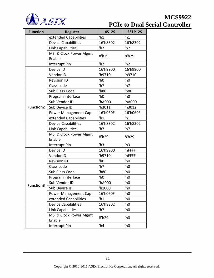
21
MCS9922PCIe to Dual Serial Controller
Copyright © 2010-2011 ASIX Electronics Corporation. All rights reserved.
Function Register 4S+2S 2S1P+2S extended Capabilities 'h1 'h1 Device Capabilities 16'h8302 16'h8302 Link Capabilities 'h7 'h7 MSI & Clock Power Mgmt Enable
8'h29 8'h29
Interrupt Pin 'h2 'h2
Function2
Device ID 16'h9900 16'h9900 Vendor ID 'h9710 'h9710 Revision ID 'h0 'h0 Class code 'h7 'h7 Sub Class Code 'h80 'h80 Program interface 'h0 'h0 Sub Vendor ID 'hA000 'hA000 Sub Device ID 'h3011 'h3012 Power Management Cap 16'h060F 16'h060F extended Capabilities 'h1 'h1 Device Capabilities 16'h8302 16'h8302 Link Capabilities 'h7 'h7 MSI & Clock Power Mgmt Enable
8'h29 8'h29
Interrupt Pin 'h3 'h3
Function3
Device ID 16'h9900 'hFFFF Vendor ID 'h9710 'hFFFF Revision ID 'h0 'h0 Class code 'h7 'h0 Sub Class Code 'h80 'h0 Program interface 'h0 'h0 Sub Vendor ID 'hA000 'h0 Sub Device ID 'h1000 'h0 Power Management Cap 16'h060F 'h0 extended Capabilities 'h1 'h0 Device Capabilities 16'h8302 'h0 Link Capabilities 'h7 'h0 MSI & Clock Power Mgmt Enable
8'h29 'h0
Interrupt Pin 'h4 'h0

22
MCS9922PCIe to Dual Serial Controller
Copyright © 2010-2011 ASIX Electronics Corporation. All rights reserved.
5.3 Serial Port Serial port is a full‐duplex device which uses separate lines for transmitting and receiving data to send and receive data at the same time. When a character is about to be transmitted, a start bit is sent. A start bit has a value of 0 (also called a space state). Thus, when the line switches from a value of 1 to a value of 0, the receiver is alerted that a data character is about to be sent. Once the start bit has been sent, the transmitter sends the actual data bits. There may either be 5, 6, 7 or 8 data bits, depending on the number you have selected. Both receiver and the transmitter must agree on the number of data bits, as well as the baud rate. Notice, when only 7 data bits are employed, and cannot send ASCII values greater than 127. Likewise, using 5 bits limits the highest possible value to 31. After the data has been transmitted, a stop bit is sent. A stop bit has a value of 1 or a mark state and it can be detected correctly even if the previous data bit also had a value of 1. This is accomplished by the stop bit's duration. Stop bits can be 1, 1.5 or 2 bit periods in length. Besides the synchronization provided by the use of start and stop bits, an additional bit called a parity bit may optionally be transmitted along with the data. A parity bit affords a small amount of error checking, to help detect data corruption that might occur during transmission. You can choose even parity, odd parity, mark parity, space parity or none at all. When even or odd parity is being used, the number of marks (logical 1 bit) in each data byte is counted, and a single bit is transmitted following the data bits to indicate whether the number of 1 bit just sent is even or odd. The Serial port implements the Enhanced mode and all of its features and it is backward compatible to the other modes. Each serial port controller has register logic controlling baud rates (50 bps – 16 Mbps), stop bits, parity bit settings. In addition, this block has serial port specific registers for interrupts, line status, line control features which can be accessed by software. The serial port controllers can interface to external RS232/RS422/RS485 transceivers. All the modes have some extra features to enhance the performance. The different modes of serial port are: • UART 16C450(Default Mode) • UART 16C550 • UART 16C550 Ex • UART 16C650 Mode • ASIX Enhanced Mode

23
MCS9922PCIe to Dual Serial Controller
Copyright © 2010-2011 ASIX Electronics Corporation. All rights reserved.
UART 16C450 Mode This mode of operation is also known as Byte mode of operation. After the power on reset, the default UART operating mode is set to 16C450. UART 16C550 Mode After the hardware reset, writing a 1 to FCR [0] register increases the FIFO size to 16, providing the compatibility with 16C550 type of devices. This mode of operation also does not have any enhanced features. Support all the features of 450 mode. UART 16C550 Extended Mode After the hardware reset, writing a 1 to FCR [0] and enabling the FIFOSEL signal the UART goes in to the 16C550 extended mode. In this mode the FIFO size increases to 128 from 16. This mode of operation also does not have any enhanced features. Support all the features of 16C550 mode. UART 16C650 Mode UART is compatible with 16C650 mode when the EFR [4] is set, i.e. the device is in the enhanced mode. In 16C650 mode, software drivers usually put the device in the enhanced mode. Running 16C650 drivers on the UART channel will result in 16C650 compatibility mode with 128 deep FIFOs, as long as the FCR [0] register is set. Support all the features of 16C550 Ex mode. ASIX Enhanced Mode The additional features offered in ASIX Enhanced mode generally apply when the UART is in enhanced mode. Flow control and High baud rate support can be achieved in this mode of operation. In enhanced mode, the FIFO size is 128 bytes. ASIX Enhanced mode specific features are enabled using the additional control register ACR.

24
MCS9922PCIe to Dual Serial Controller
Copyright © 2010-2011 ASIX Electronics Corporation. All rights reserved.
5.4 I2C All I2C devices are connected through two wires: serial data (SDA) and serial clock (SCL). I2C has a master/slave protocol. The master initiates the communication. Since there are only two wires, this protocol includes the extra overhead of the addressing and acknowledgment mechanisms. Serial Data: The serial data SDA is a bi‐directional pin used to transfer addresses and data into and data out of the device. It is an open drain terminal; therefore, the SDA bus requires a pull‐up resistor to VCC (typical 10 kΩ for 100 kHz, 2 kΩ for 400 kHz and 1 MHz). For normal data transfer SDA is allowed to change only during SCL low. Changes during SCL high are reserved for indicating the START and STOP conditions. Serial Clock: The serial clock SCL is a bi‐directional pin used to synchronize the data transfer from and to the device. Address inputs: The address inputs A0, A1, A2 are used by the slave for multiple device operations. The logic levels on these inputs are compared with the corresponding bits in the slave address. EEPROM Access I2C operation is performed at address: GPIO_I2C_BAR5+0xC8. The 32‐bit information sent at this address is specified in tsif_cfg_data_in register. The details of this register are as follows: Bits Type Reset Name Description [31] RW 0 tsif_cfg_data_in If ‘1’ specifies write to EPROM.
If ‘0’ specifies read from EEPROM. [30:25] RW 0 tsif_cfg_data_in specifies I2C device address [24] RW 0 tsif_cfg_data_in specifies I2C address is 8‐bit/16‐bit [23:8] RW 0 tsif_cfg_data_in specifies I2C address [7:0] RW 0 tsif_cfg_data_in specifies 8‐bit data

25
MCS9922PCIe to Dual Serial Controller
Copyright © 2010-2011 ASIX Electronics Corporation. All rights reserved.
5.5 PM Control This block implements power management. The chip works in three PCIe based power states (1) D0, (2) D3 Hot and (3) D3 Cold. There is NO power plane separation between Vaux and VCC. In D3 Cold, the chip VCC should be powered from Vaux to support remote wake up. Further power save is achieved through disabling the blocks which are not selected. A set of register bits, Port_dis_reg[7:0], are provided to disable each block independently. Port_dis_reg is mapped to BAR4 + 0x69 and can access through all functions and its bit map is given below
Register Bit Control Description port_dis_reg[0] pp_disable 1: Disables Parallel Port port_dis_reg[1] Serial Port transceiver shut down
polarity 1: Active Low 0: Active High
port_dis_reg[2] Serial Port transceiver shut down enable
1: Enables transceiver shut down when in power save mode
0: disables transceiver shut downport_dis_reg[3] sp1_disable 1 : Disables Serial Port 1 port_dis_reg[4] sp2_disable 1 : Disables Serial Port 2 port_dis_reg[5] Reserved Reserved port_dis_reg[6] Reserved Reserved port_dis_reg[7] disp_disable 1 : Reserved

26
MCS9922PCIe to Dual Serial Controller
Copyright © 2010-2011 ASIX Electronics Corporation. All rights reserved.
5.6 Cascade Interface Cascade Interface is a generic IO expansion bus that is based on ASIX proprietary interface protocol. The cascade interface allows interconnecting any ASIX device supporting the cascade interface protocol. A standalone MCS9922 device supports up to 2 serial ports over PCIe. When a MCS9922 device is interconnected through MCS9900 device cascade interface, the number of peripheral ports can be increased. The combined MCS9922 and MCS9900 devices are serviced through a single PCIe on the primary MCS9900, and the ports can be expanded using one of the following configurations.
• 6 serial ports • 4 serial ports and 1 parallel ports
In cascaded configuration, MCS9900 chip works as primary and MCS9922 as secondary. The primary chip implements 4‐function PCIe endpoint. The PCIe core of secondary chip is disabled. Only cascade and serial port logic is active in secondary chip The cascade interface also allows connecting any other chip that’s designed as per this interface. When a non MCS9900 chip is connected, functions 0, 1 and 2 are used by primary and functions 3 and 4 are available to be used by secondary chip.
Cascade Interface between Primary and Secondary Devices

27
MCS9922PCIe to Dual Serial Controller
Copyright © 2010-2011 ASIX Electronics Corporation. All rights reserved.
In cascade mode, the PCIe endpoint interface is available through the primary MCS9900 device only. The PCIe is disabled on the MCS9922 cascaded secondary device and its access is limited through the cascade interface only. The primary MCS9900 implements a 4‐function PCIe end point such that each of these 4 functions serve two serial port, one from primary chip and the other from secondary chip. The following tables list the functions and the corresponding BAR mapping. BAR Mapping for 6‐Serial mode PCIe functions
BAR Function 0 Function 1 Function 2 Function 3 BAR0 SP1 I/O SP2 I/O SP3 I/O SP4 I/O BAR1 SP1 Mem SP2 Mem SP3 Mem SP4 Mem BAR2 ‐ ‐ ‐ ‐ BAR3 SP5 I/O SP6 I/O ‐ ‐ BAR4 SP5 Mem SP6 Mem ‐ ‐ BAR5 GPIO/I2C GPIO/I2C ‐ GPIO/I2C
BAR Mapping for 4‐Serial 1‐Parallel mode PCIe functions
BAR Function 0 Function 1 Function 2 BAR0 SP1 I/O SP2 I/O PP1 I/O BAR1 SP1 Mem SP2 Mem PP1 I/O BAR2 ‐ ‐ PP1 Mem BAR3 SP3 I/O SP4 I/O ‐ BAR4 SP3 Mem SP4 Mem ‐ BAR5 GPIO/I2C GPIO/I2C ‐
BAR Mapping for 2 Serial & Other Secondary device mode PCIe functions
BAR Function 0 Function 1 Function 2 Function 3 BAR0 SP1 I/O SP2 I/O Secondary chip Secondary chip BAR1 SP1 Mem SP2 Mem Secondary chip Secondary chip BAR2 ‐ ‐ Secondary chip Secondary chip BAR3 ‐ ‐ Secondary chip Secondary chip BAR4 ‐ ‐ Secondary chip Secondary chip BAR5 GPIO/I2C GPIO/I2C ‐ GPIO/I2C

28
MCS9922PCIe to Dual Serial Controller
Copyright © 2010-2011 ASIX Electronics Corporation. All rights reserved.
1 Serial & Other Secondary device mode PCIe functions
BAR Function 0 Function 1 Function 2 Function 3 BAR0 SP1 I/O ‐ Secondary chip Secondary chip BAR1 SP1 Mem ‐ Secondary chip Secondary chip BAR2 ‐ ‐ Secondary chip Secondary chip BAR3 ‐ ‐ Secondary chip Secondary chip BAR4 ‐ ‐ Secondary chip Secondary chip BAR5 GPIO/I2C GPIO/I2C ‐ GPIO/I2C
Cascade clock connection In order to meet timing on cascade interface, it is required to send cascade clock out from primary (through CASC_CLK pin) and bring it back using SCAN_MODE pins to both primary and secondary chips through an external onboard connection. Figure below shows the required connections.

29
MCS9922PCIe to Dual Serial Controller
Copyright © 2010-2011 ASIX Electronics Corporation. All rights reserved.
5.7 Clocks and Resets MCS9922 requires two input clocks. One input clock is sourced from the PCIe connector and the second input clock is sourced from the external crystal. PCIe PHY uses the 100 MHz differential clock from the PCIe connector to generate the internal 125MHz clock. Clock from crystal is used to generate clocks for serial ports. Crystal Requirement MCS9922 requires one crystal. This crystal is used to generate serial port clocks. Preferable input frequency is 30 MHz because it allows generating the serial port clock frequency of 96 MHz. Crystal Frequency For Serial Ports 30 MHz Internal PLLs MCS9922 uses two PLLs to generate the necessary internal clocks for the device operation. The usage of the PLLs is listed in the following Table. PLL Input Frequency Output Frequency Used By PLL1 30 MHz 96 MHz Serial Port POR Cell A POR Cell is used to isolate reset of EEPROM from PCIe reset. It is observed that some PCIe hosts issue multiple PCIe resets. EEPROM read starts automatically on power up. If PCIe reset is used for EEPROM state machines, it causes abrupt resets to EEPROM state machine and may cause it to hang. To avoid this, EEPROM logic is being reset on power‐on only. PCIe resets do not affect EEPROM logic.
Side effect of this is that EEPROM logic and the register set that’s loaded from EEPROM holds the values till power cycle. If there is a change in EEPROM or EEPROM data, it is required to power cycle in order to get the new values.

30
MCS9922PCIe to Dual Serial Controller
Copyright © 2010-2011 ASIX Electronics Corporation. All rights reserved.
5.8 GPIO There are 8 General Purpose Input/Output pins. All the GPIO pins are interrupt capable. Each GPIO can be configured independent of all other GPIO. The GPIOs allow data input and IRQ generation. The GPIO Interface register layout can be configured so that the direction and level of each I/O can be configured using either a single register for all I/Os, or discrete registers for each I/O. Extended Modes through EEPROM
MCS9922 can be configured using external EEPROM, Few such configurations are listed below. MCS9922 Possible Product Configuration EEPROM Required? Mode Selection at System Level?1 Serial Port Yes No 2 Serial Ports No No

31
MCS9922PCIe to Dual Serial Controller
Copyright © 2010-2011 ASIX Electronics Corporation. All rights reserved.
6 EEPROM Contents Layout MCS9922 requires an I2C EEPROM (in 16 bit organization mode) for configuring various sub configurations and device parameters.
EEPROM Address Parameter MCS9922 (2S) 0 Signature ID_F0[7:0] 10 1 Signature ID_F0[15:8] 97 2 Vendor ID_F0[7:0] 10 3 Vendor ID_F0[15:8] 97 4 Device ID_F0[7:0] 22 5 Device ID_F0[15:8] 99 6 Revision ID 00 7 Programmable IF_F0 02 8 Sub Class Code_F0 00 9 Class Code_F0 07 10 Sub System Vendor ID_F0[7:0] 00 11 Sub System Vendor ID_F0[15:8] A0 12 Sub System Device ID_F0[7:0] 00 13 Sub System Device ID_F0[15:8] 10 14 PM_Cap_F0[7:0] 0F 15 PM_Cap_F0[15:8] 06 16 Extended capabilities F0[7:0] 01 17 Extended capabilities F015:8] 00 18 Device Capabilities F0[7:0] 02 19 Device Capabilities F0[15:8] 83 20 Link_Capabilities F0[7:0] 07 21 msi_and_clk_pwr_mgmt_en F0[7:0] 19 22 Interrupt pin F0 01 23 Vendor ID_F1[7:0] 10 24 Vendor ID_F1[15:8] 97 25 Device ID_F1[7:0] 22 26 Device ID_F1[15:8] 99 27 Programmable IF_F1 02 28 Sub Class Code_F1 00 29 Class Code_F1 07 30 Sub System Vendor ID_F1[7:0] 00 31 Sub System Vendor ID_F1[15:8] A0 32 Sub System Device ID_F1[7:0] 00 33 Sub System Device ID_F1[15:8] 10 34 PM_Cap_F1[7:0] 0F 35 PM_Cap_F1[15:8] 06 36 Extended capabilities F1[7:0] 01 37 Extended capabilities F115:8] 00 38 Device Capabilities F1[7:0] 02 39 Device Capabilities F1[15:8] 83

32
MCS9922PCIe to Dual Serial Controller
Copyright © 2010-2011 ASIX Electronics Corporation. All rights reserved.
EEPROM Address Parameter MCS9922 (2S) 40 Link_Capabilities F17:0] 07 41 msi_and_clk_pwr_mgmt_en F1[7:0] 19 42 Interrupt pin F1 02 43 Vendor ID_F2[7:0] FF 44 Vendor ID_F2[15:8] FF 45 Device ID_F2[7:0] FF 46 Device ID_F2[15:8] FF 47 Programmable IF_F2 00 48 Sub Class Code_F2 00 49 Class Code_F2 00 50 Sub System Vendor ID_F2[7:0] 00 51 Sub System Vendor ID_F2[15:8] 00 52 Sub System Device ID_F2[7:0] 00 53 Sub System Device ID_F2[15:8] 00 54 PM_Cap_F2[7:0] 00 55 PM_Cap_F2[15:8] 00 56 Extended capabilities F2[7:0] 00 57 Extended capabilities F215:8] 00 58 Device Capabilities F2[7:0] 00 59 Device Capabilities F2[15:8] 00 60 Link_Capabilities F2[7:0] 00 61 msi_and_clk_pwr_mgmt_en F2[7:0] 00 62 Interrupt pin F2 00 63 Vendor ID_F3[7:0] FF 64 Vendor ID_F3[15:8] FF 65 Device ID_F3[7:0] FF 66 Device ID_F3[15:8] FF 67 Programmable IF_F3 00 68 Sub Class Code_F3 00 69 Class Code_F3 00 70 Sub System Vendor ID_F3[7:0] 00 71 Sub System Vendor ID_F3[15:8] 00 72 Sub System Device ID_F3[7:0] 00 73 Sub System Device ID_F3[15:8] 00 74 PM_Cap_F3[7:0] 00 75 PM_Cap_F3[15:8] 00 76 Extended capabilities F3[7:0] 00 77 Extended capabilities F3[15:8] 00 78 Device Capabilities F3[7:0] 00 79 Device Capabilities F3[15:8] 00 80 Link_Capabilities F3[7:0] 00 81 msi_and_clk_pwr_mgmt_en F3[7:0] 00 82 Interrupt pin F3 00 83 Vendor ID_F4[7:0] FF 84 Vendor ID_F4[15:8] FF 85 Device ID_F4[7:0] FF

33
MCS9922PCIe to Dual Serial Controller
Copyright © 2010-2011 ASIX Electronics Corporation. All rights reserved.
EEPROM Address Parameter MCS9922 (2S) 86 Device ID_F4[15:8] FF 87 Programmable IF_F3 00 88 Sub Class Code_F3 00 89 Class Code_F3 00 90 Sub System Vendor ID_F4[7:0] 00 91 Sub System Vendor ID_F4[15:8] 00 92 Sub System Device ID_F4[7:0] 00 93 Sub System Device ID_F4[15:8] 00 94 PM_Cap_F4[7:0] 00 95 PM_Cap_F4[15:8] 00 96 Extended capabilities F4[7:0] 00 97 Extended capabilities F4[15:8] 00 98 Device Capabilities F4[7:0] 00 99 Device Capabilities F4[15:8] 00 100 Link_Capabilities F4[7:0] 00 101 msi_and_clk_pwr_mgmt_en F4[7:0] 00 102 Interrupt pin F4 00 103 INTA Mask register 02 104 INTB Mask Register 04 105 INTC Mask Register 00 106 INTD Mask Register 00 107 Port Disable Register 02 108 Reserved 14 109 Serial port1 Function number 00 110 Serial port2 Function number 01 111 Serial port3 Function number 02 112 Serial port4 Function number 03 113 Reserved 00
114 to 170 bar3,bar4 incase of 3rd party modes ‐

34
MCS9922PCIe to Dual Serial Controller
Copyright © 2010-2011 ASIX Electronics Corporation. All rights reserved.
7 Electrical Specifications
Absolute Maximum Ratings
Symbol Description Rating unit
VCCK 1.2V Digital Power Supply ‐0.3 to 1.44 V
VCC12A 1.2V Analog Power Supply ‐0.3 to 1.44 V
VCC33IO 3.3V Digital Power Supply ‐0.3 to 4.0 V
VCC33A 3.3V Analog Power Supply ‐0.3 to 4.0 V
T stg Storage temperature ‐40 to 150 oC
To Operating temperature 0 to 85 oC
Tj Junction temperature 0 to 125 oC
ESD HBM (MIL‐STD 883E Method 3015‐7 Class 2) 2000 V
ESD MM (JEDEC EIA/JESD22 A115‐A) 200 V
CDM (JEDEC JESD22 C101‐A) 500 V
θJA Thermal Resistance of Junction to Ambient 52.7 C/W
θJC Thermal Resistance of Junction to Case 17.8 C/W
ΨJT Junction to Top of the Package Characterization Parameter
0.54 C/W
C/W – o C per Watt , For Still Air Condition

35
MCS9922PCIe to Dual Serial Controller
Copyright © 2010-2011 ASIX Electronics Corporation. All rights reserved.
Recommended Operating Conditions
Symbol Description Min Typ Max units
VCCK 1.2V Digital Power Supply 1.08 1.2 1.32 V
VCC12A 1.2V Analog Power Supply 1.08 1.2 1.32 V
VCC33IO 3.3V Digital Power Supply 2.97 3.3 3.63 V
VCC33A 3.3V Analog Power Supply 2.97 3.3 3.63 V
I1.2VD Current in 1.2V Digital Power Supply
65 mA
I1.2VA Current in 1.2V Analog Power Supply
40 mA
I3.3VD Current of 3.3V Digital Power Supply
20 mA
I3.3VA Current in 3.3V Analog Power Supply
75 mA

36
MCS9922PCIe to Dual Serial Controller
Copyright © 2010-2011 ASIX Electronics Corporation. All rights reserved.
8 Mechanical Dimensions

37
MCS9922PCIe to Dual Serial Controller
Copyright © 2010-2011 ASIX Electronics Corporation. All rights reserved.
Revision History
Revision Date Comment 1.0 20 July 2010 Initial release
2.00 2011/08/05 1. Changed to ASIX Electronics Corp. logo, strings and contact information.
2. Added ASIX copyright legal header information. 3. Modified the Revision History table format. 4. Updated the block diagram in Section 1.1.

38
MCS9922PCIe to Dual Serial Controller
Copyright © 2010-2011 ASIX Electronics Corporation. All rights reserved.
4F, No. 8, Hsin Ann Rd., HsinChu Science Park, HsinChu, Taiwan, R.O.C.
TEL: 886-3-5799500 FAX: 886-3-5799558
Sales Email: [email protected]
Support Email: [email protected] Web: http://www.asix.com.tw