MCP6541/1R/1U/2/3/4- Push-Pull Output Sub …ww1.microchip.com/downloads/en/DeviceDoc/21696H.pdf ·...
46
© 2002-2011 Microchip Technology Inc. DS21696H-page 1 MCP6541/1R/1U/2/3/4 Features: • Low Quiescent Current: 600 nA/Comparator (typ.) • Rail-to-Rail Input: V SS - 0.3V to V DD + 0.3V • CMOS/TTL-Compatible Output • Propagation Delay: 4 μs (typical, 100 mV Overdrive) • Wide Supply Voltage Range: 1.6V to 5.5V • Available in Single, Dual and Quad • Single Available in SOT-23-5, SC-70-5 * Packages • Chip Select (CS ) with MCP6543 • Low Switching Current • Internal Hysteresis: 3.3 mV (typ.) • Temperature Ranges: - Industrial: -40°C to +85°C - Extended: -40°C to +125°C Typical Applications: • Laptop Computers • Mobile Phones • Metering Systems • Hand-held Electronics • RC Timers • Alarm and Monitoring Circuits • Windowed Comparators • Multivibrators Related Devices: • Open-Drain Output: MCP6546/7/8/9 Description: The Microchip Technology Inc. MCP6541/1R/1U/2/3/4 family of comparators is offered in single (MCP6541, MCP6541R, MCP6541U), single with Chip Select (CS ) (MCP6543), dual (MCP6542) and quad (MCP6544) configurations. The outputs are push-pull (CMOS/TTL- compatible) and are capable of driving heavy DC or capacitive loads. These comparators are optimized for low-power, single-supply operation with greater than rail-to-rail input operation. The push-pull output of the MCP6541/1R/1U/2/3/4 family supports rail-to-rail out- put swing and interfaces with TTL/CMOS logic. The internal input hysteresis eliminates output switching due to internal input noise voltage, reducing current draw. The output limits supply current surges and dynamic power consumption while switching. This product family operates with a single-supply voltage as low as 1.6V and draws less than 1 μA/comparator of quiescent current. The related MCP6546/7/8/9 family of comparators from Microchip has an open-drain output. Used with a pull- up resistor, these devices can be used as level-shifters for any desired voltage up to 10V and in wired-OR logic. * SC-70-5 E-Temp parts not available at this release of the data sheet. MCP6541U SOT-23-5 is E-Temp only. Package Types V INA + V IN – MCP6541 V SS V DD OUT 1 2 3 4 8 7 6 5 NC NC NC PDIP, SOIC, MSOP 4 1 2 3 - + 5 SOT-23-5 V DD OUT V IN + V SS V IN – MCP6542 V INA + V INA – V SS 1 2 3 4 8 7 6 5 - OUTA +- + V DD OUTB V INB – V INB + V IN + V IN – MCP6543 V SS V DD OUT 1 2 3 4 8 7 6 5 - + NC CS NC PDIP, SOIC, MSOP PDIP, SOIC, MSOP MCP6544 V INA + V INA – V SS 1 2 3 4 14 13 12 11 - OUTA +- + V DD OUTD V IND – V IND + 10 9 8 5 6 7 OUTB V INB – V INB + V INC + V INC - OUTC + - - + PDIP, SOIC, TSSOP - + MCP6541R 4 1 2 3 5 SC-70-5, SOT-23-5 V SS V IN + V IN – V DD OUT MCP6541U - + 4 1 2 3 - + 5 V SS OUT V IN + V DD V IN – MCP6541 SC-70-5, SOT-23-5 Push-Pull Output Sub-Microamp Comparators
Transcript of MCP6541/1R/1U/2/3/4- Push-Pull Output Sub …ww1.microchip.com/downloads/en/DeviceDoc/21696H.pdf ·...

MCP6541/1R/1U/2/3/4Push-Pull Output Sub-Microamp Comparators
Features:• Low Quiescent Current: 600 nA/Comparator (typ.)• Rail-to-Rail Input: VSS - 0.3V to VDD + 0.3V• CMOS/TTL-Compatible Output• Propagation Delay: 4 µs
(typical, 100 mV Overdrive)• Wide Supply Voltage Range: 1.6V to 5.5V• Available in Single, Dual and Quad• Single Available in SOT-23-5, SC-70-5 * Packages• Chip Select (CS) with MCP6543• Low Switching Current• Internal Hysteresis: 3.3 mV (typ.)• Temperature Ranges:
- Industrial: -40°C to +85°C- Extended: -40°C to +125°C
Typical Applications:• Laptop Computers• Mobile Phones• Metering Systems• Hand-held Electronics• RC Timers• Alarm and Monitoring Circuits• Windowed Comparators• Multivibrators
Related Devices:• Open-Drain Output: MCP6546/7/8/9
Description:The Microchip Technology Inc. MCP6541/1R/1U/2/3/4family of comparators is offered in single (MCP6541, MCP6541R, MCP6541U), single with Chip Select (CS)(MCP6543), dual (MCP6542) and quad (MCP6544)configurations. The outputs are push-pull (CMOS/TTL-compatible) and are capable of driving heavy DC orcapacitive loads.
These comparators are optimized for low-power,single-supply operation with greater than rail-to-railinput operation. The push-pull output of theMCP6541/1R/1U/2/3/4 family supports rail-to-rail out-put swing and interfaces with TTL/CMOS logic. Theinternal input hysteresis eliminates output switchingdue to internal input noise voltage, reducing currentdraw. The output limits supply current surges anddynamic power consumption while switching. Thisproduct family operates with a single-supply voltage aslow as 1.6V and draws less than 1 µA/comparator ofquiescent current.
The related MCP6546/7/8/9 family of comparators fromMicrochip has an open-drain output. Used with a pull-up resistor, these devices can be used as level-shiftersfor any desired voltage up to 10V and in wired-ORlogic.
* SC-70-5 E-Temp parts not available at this release ofthe data sheet.
MCP6541U SOT-23-5 is E-Temp only.
Package Types
VINA+VIN–
MCP6541
VSS
VDD
OUT
1234
8
765
-+
NC
NCNC
PDIP, SOIC, MSOP
4
1
2
3
-+
5
SOT-23-5
VDD
OUT
VIN+
VSS
VIN–
MCP6542
VINA+VINA–
VSS
1234
8765
-
OUTA
+ -+
VDD
OUTBVINB–VINB+
VIN+VIN–
MCP6543
VSS
VDD
OUT
1234
8765
-+
NC
CSNC
PDIP, SOIC, MSOP
PDIP, SOIC, MSOP
MCP6544
VINA+VINA–
VSS
1234
14131211
-OUTA
+ -+
VDD
OUTDVIND–VIND+
1098
567OUTB
VINB–VINB+ VINC+
VINC-OUTC
+- -+
PDIP, SOIC, TSSOP-+
MCP6541R
4
1
2
3
5
SC-70-5, SOT-23-5
VSS
VIN+
VIN–
VDD
OUT
MCP6541U
-
+
4
1
2
3
-+
5VSS
OUT
VIN+
VDD
VIN–
MCP6541SC-70-5, SOT-23-5
© 2002-2011 Microchip Technology Inc. DS21696H-page 1

MCP6541/1R/1U/2/3/4
NOTES:DS21696H-page 2 © 2002-2011 Microchip Technology Inc.

MCP6541/1R/1U/2/3/4
1.0 ELECTRICAL CHARACTERISTICS
Absolute Maximum Ratings †VDD - VSS .........................................................................7.0VCurrent at Analog Input Pin (VIN+, VIN-.........................±2 mAAnalog Input (VIN) †† ...................... VSS - 1.0V to VDD + 1.0VAll other Inputs and Outputs........... VSS - 0.3V to VDD + 0.3VDifference Input Voltage ....................................... |VDD - VSS|Output Short-Circuit Current ................................ContinuousCurrent at Input Pins ....................................................±2 mACurrent at Output and Supply Pins ............................±30 mAStorage Temperature ....................................-65°C to +150°CMaximum Junction Temperature (TJ) .......................... +150°CESD Protection on all Pins (HBM;MM) ..................4 kV; 400V
† Notice: Stresses above those listed under “AbsoluteMaximum Ratings” may cause permanent damage to thedevice. This is a stress rating only and functional operation ofthe device at those or any other conditions above thoseindicated in the operational listings of this specification is notimplied. Exposure to maximum rating conditions for extendedperiods may affect device reliability.
†† See Section 4.1.2 “Input Voltage and CurrentLimits”
DC CHARACTERISTICSElectrical Specifications: Unless otherwise indicated, VDD = +1.6V to +5.5V, VSS = GND, TA = +25°C,VIN+ = VDD/2,VIN– = VSS, and RL = 100 kΩ to VDD/2 (Refer to Figure 1-3).
Parameters Sym Min Typ Max Units ConditionsPower SupplySupply Voltage VDD 1.6 — 5.5 VQuiescent Current per comparator IQ 0.3 0.6 1.0 µA IOUT = 0InputInput Voltage Range VCMR VSS−0.3 — VDD+0.3 VCommon Mode Rejection Ratio CMRR 55 70 — dB VDD = 5V, VCM = -0.3V to 5.3VCommon Mode Rejection Ratio CMRR 50 65 — dB VDD = 5V, VCM = 2.5V to 5.3VCommon Mode Rejection Ratio CMRR 55 70 — dB VDD = 5V, VCM = -0.3V to 2.5VPower Supply Rejection Ratio PSRR 63 80 — dB VCM = VSS
Input Offset Voltage VOS -7.0 ±1.5 +7.0 mV VCM = VSS (Note 1)Drift with Temperature ΔVOS/ΔTA — ±3 — µV/°C TA = -40°C to +125°C, VCM = VSS
Input Hysteresis Voltage VHYST 1.5 3.3 6.5 mV VCM = VSS (Note 1)Linear Temp. Co. (Note 2) TC1 — 6.7 — µV/°C TA = -40°C to +125°C, VCM = VSS
Quadratic Temp. Co. (Note 2) TC2 — -0.035 — µV/°C2 TA = -40°C to +125°C, VCM = VSS
Input Bias Current IB — 1 — pA VCM = VSS
At Temperature (I-Temp parts) IB — 25 100 pA TA = +85°C, VCM = VSS (Note 3)At Temperature (E-Temp parts) IB — 1200 5000 pA TA = +125°C, VCM = VSS (Note 3)
Input Offset Current IOS — ±1 — pA VCM = VSS
Common Mode Input Impedance ZCM — 1013||4 — Ω||pFDifferential Input Impedance ZDIFF — 1013||2 — Ω||pFNote 1: The input offset voltage is the center (average) of the input-referred trip points. The input hysteresis is the difference
between the input-referred trip points.2: VHYST at different temperatures is estimated using VHYST (TA) = VHYST + (TA - 25°C) TC1 + (TA - 25°C)2 TC2.3: Input bias current at temperature is not tested for SC-70-5 package.4: Limit the output current to Absolute Maximum Rating of 30 mA.
© 2002-2011 Microchip Technology Inc. DS21696H-page 3

MCP6541/1R/1U/2/3/4
AC CHARACTERISTICS
Push-Pull OutputHigh-Level Output Voltage VOH VDD−0.2 — — V IOUT = -2 mA, VDD = 5VLow-Level Output Voltage VOL — — VSS+0.2 V IOUT = 2 mA, VDD = 5VShort-Circuit Current ISC — -2.5, +1.5 — mA VDD = 1.6V (Note 4)
ISC — ±30 — mA VDD = 5.5V (Note 4)
Electrical Specifications: Unless otherwise indicated, VDD = +1.6V to +5.5V, VSS = GND, TA = +25°C, VIN+ = VDD/2, Step = 200 mV, Overdrive = 100 mV, and CL = 36 pF (Refer to Figure 1-2 and Figure 1-3).
Parameters Sym Min Typ Max Units Conditions
Rise Time tR — 0.85 — µsFall Time tF — 0.85 — µsPropagation Delay (High-to-Low) tPHL — 4 8 µsPropagation Delay (Low-to-High) tPLH — 4 8 µsPropagation Delay Skew tPDS — ±0.2 — µs (Note 1)Maximum Toggle Frequency fMAX — 160 — kHz VDD = 1.6V
fMAX — 120 — kHz VDD = 5.5VInput Noise Voltage Eni — 200 — µVP-P 10 Hz to 100 kHzNote 1: Propagation Delay Skew is defined as: tPDS = tPLH - tPHL.
DC CHARACTERISTICS (CONTINUED)Electrical Specifications: Unless otherwise indicated, VDD = +1.6V to +5.5V, VSS = GND, TA = +25°C,VIN+ = VDD/2,VIN– = VSS, and RL = 100 kΩ to VDD/2 (Refer to Figure 1-3).
Parameters Sym Min Typ Max Units Conditions
Note 1: The input offset voltage is the center (average) of the input-referred trip points. The input hysteresis is the difference between the input-referred trip points.
2: VHYST at different temperatures is estimated using VHYST (TA) = VHYST + (TA - 25°C) TC1 + (TA - 25°C)2 TC2.3: Input bias current at temperature is not tested for SC-70-5 package.4: Limit the output current to Absolute Maximum Rating of 30 mA.
DS21696H-page 4 © 2002-2011 Microchip Technology Inc.

MCP6541/1R/1U/2/3/4
FIGURE 1-1: Timing Diagram for the CS Pin on the MCP6543.
FIGURE 1-2: Propagation Delay Timing Diagram.
MCP6543 CHIP SELECT (CS) CHARACTERISTICSElectrical Specifications: Unless otherwise indicated, VDD = +1.6V to +5.5V, VSS = GND, TA = +25°C, VIN+ = VDD/2, VIN– = VSS, and CL= 36 pF (Refer to Figures 1-1 and 1-3).
Parameters Sym Min Typ Max Units Conditions
CS Low SpecificationsCS Logic Threshold, Low VIL VSS — 0.2 VDD V
CS Input Current, Low ICSL — 5.0 — pA CS = VSS
CS High SpecificationsCS Logic Threshold, High VIH 0.8 VD
D— VDD V
CS Input Current, High ICSH — 1 — pA CS = VDD
CS Input High, VDD Current IDD — 18 — pA CS = VDD
CS Input High, GND Current ISS — –20 — pA CS = VDD
Comparator Output Leakage IO(LEAK) — 1 — pA VOUT = VDD, CS = VDD
CS Dynamic SpecificationsCS Low to Comparator Output Low Turn-on Time
tON — 2 50 ms CS = 0.2 VDD to VOUT = VDD/2,VIN– = VDD
CS High to Comparator Output High Z Turn-off Time
tOFF — 10 — µs CS = 0.8 VDD to VOUT = VDD/2,VIN– = VDD
CS Hysteresis VCS_HYST
— 0.6 — V VDD = 5V
VIL
Hi-Z
tON
VIHCS
tOFF
VOUT
-20 pA (typ.)
Hi-Z
ISS
ICS1 pA (typ.) 1 pA (typ.)
-20 pA (typ.)-0.6 µA (typ.)
VOL
tPLH
VOUT
VIN–100 mV
100 mV tPHL
VOL
VIN+ = VDD/2
VOH
© 2002-2011 Microchip Technology Inc. DS21696H-page 5

MCP6541/1R/1U/2/3/4
TEMPERATURE CHARACTERISTICS
1.1 Test Circuit ConfigurationThis test circuit configuration is used to determine theAC and DC specifications.
FIGURE 1-3: AC and DC Test Circuit for the Push-Pull Output Comparators.
Electrical Specifications: Unless otherwise indicated, VDD = +1.6V to +5.5V and VSS = GND.
Parameters Sym Min Typ Max Units Conditions
Temperature RangesSpecified Temperature Range TA -40 — +85 °COperating Temperature Range TA -40 — +125 °C NoteStorage Temperature Range TA -65 — +150 °CThermal Package ResistancesThermal Resistance, 5L-SC-70 θJA — 331 — °C/WThermal Resistance, 5L-SOT-23 θJA — 220.7 — °C/WThermal Resistance, 8L-PDIP θJA — 89.3 — °C/WThermal Resistance, 8L-SOIC θJA — 149.5 — °C/WThermal Resistance, 8L-MSOP θJA — 211 — °C/WThermal Resistance, 14L-PDIP θJA — 70 — °C/WThermal Resistance, 14L-SOIC θJA — 95.3 — °C/WThermal Resistance, 14L-TSSOP θJA — 100 — °C/W
Note: The MCP6541/1R/1U/2/3/4 I-Temp parts operate over this extended temperature range, but with reducedperformance. In any case, the Junction Temperature (TJ) must not exceed the Absolute Maximumspecification of +150°C.
VDD
VSS = 0V
200 kΩ
200 kΩ200 kΩ
200 kΩVOUT
VIN = VSS
36 pF
MCP654X
DS21696H-page 6 © 2002-2011 Microchip Technology Inc.

MCP6541/1R/1U/2/3/4
2.0 TYPICAL PERFORMANCE CURVES
Note: Unless otherwise indicated, VDD = +1.6V to +5.5V, VSS = GND, TA = +25°C, VIN+ = VDD/2, VIN– = GND,RL = 100 kΩ to VDD/2, and CL = 36 pF.
FIGURE 2-1: Input Offset Voltage at VCM = VSS.
FIGURE 2-2: Input Offset Voltage Drift at VCM = VSS.
FIGURE 2-3: The MCP6541/1R/1U/2/3/4 Comparators Show No Phase Reversal.
FIGURE 2-4: Input Hysteresis Voltage at VCM = VSS.
FIGURE 2-5: Input Hysteresis Voltage Linear Temp. Co. (TC1) at VCM = VSS.
FIGURE 2-6: Input Hysteresis Voltage Quadratic Temp. Co. (TC2) at VCM = VSS.
Note: The graphs and tables provided following this note are a statistical summary based on a limited number ofsamples and are provided for informational purposes only. The performance characteristics listed hereinare not tested or guaranteed. In some graphs or tables, the data presented may be outside the specifiedoperating range (e.g., outside specified power supply range) and therefore outside the warranted range.
0%
2%
4%
6%
8%
10%
12%
14%
-7 -6 -5 -4 -3 -2 -1 0 1 2 3 4 5 6 7Input Offset Voltage (mV)
Perc
enta
ge o
f Occ
urre
nces 1200 Samples
VCM = VSS
0%2%4%6%8%
10%12%14%16%
-14
-12
-10 -8 -6 -4 -2 0 2 4 6 8 10 12 14
Input Offset Voltage Drift (µV/°C)
Perc
enta
ge o
f Occ
urre
nces 1200 Samples
VCM = VSSTA= -40°C to +125°C
-1
0
1
2
3
4
5
6
7
0 1 2 3 4 5 6 7 8 9 10Time (1 ms/div)
Inve
rtin
g In
put,
Out
put V
olta
ge
(V)
VOUT
VIN–
VDD = 5.5V
0%2%4%6%8%
10%12%14%16%18%
1.6 2.0 2.4 2.8 3.2 3.6 4.0 4.4 4.8 5.2 5.6 6.0Input Hysteresis Voltage (mV)
Perc
enta
ge o
f Occ
urre
nces 1200 Samples
VCM = VSS
0%
5%
10%
15%
20%
25%4.
6
5.0
5.4
5.8
6.2
6.6
7.0
7.4
7.8
8.2
8.6
9.0
9.4
Input Hysteresis Voltage –Linear Temp. Co.; TC1 (µV/°C)
Perc
enta
ge o
f Occ
urre
nces 596 Samples
VCM = VSSTA = -40°C to +125°C
VDD = 1.6VVDD = 5.5V
0%2%4%6%8%
10%12%14%16%18%20%
-0.0
60
-0.0
56
-0.0
52
-0.0
48
-0.0
44
-0.0
40
-0.0
36
-0.0
32
-0.0
28
-0.0
24
-0.0
20
-0.0
16
Input Hysteresis Voltage –Quadratic Temp. Co.; TC2 (µV/°C2)
Perc
enta
ge o
f Occ
urre
nces
596 SamplesVCM = VSS
TA = -40°C to +125°C
VDD = 5.5V
VDD = 1.6V
© 2002-2011 Microchip Technology Inc. DS21696H-page 7

MCP6541/1R/1U/2/3/4
Note: Unless otherwise indicated, VDD = +1.6V to +5.5V, VSS = GND, TA = +25°C, VIN+ = VDD/2, VIN– = GND,RL = 100 kΩ to VDD/2, and CL = 36 pF.FIGURE 2-7: Input Offset Voltage vs. Ambient Temperature at VCM = VSS.
FIGURE 2-8: Input Offset Voltage vs. Common Mode Input Voltage at VDD = 1.6V.
FIGURE 2-9: Input Offset Voltage vs. Common Mode Input Voltage at VDD = 5.5V.
FIGURE 2-10: Input Hysteresis Voltage vs. Ambient Temperature at VCM = VSS.
FIGURE 2-11: Input Hysteresis Voltage vs. Common Mode Input Voltage at VDD = 1.6V.
FIGURE 2-12: Input Hysteresis Voltage vs. Common Mode Input Voltage at VDD = 5.5V.
-1.0-0.8-0.6-0.4-0.20.00.20.40.60.81.0
-50 -25 0 25 50 75 100 125Ambient Temperature (°C)
Inpu
t Offs
et V
olta
ge (m
V)
VDD = 1.6V
VDD = 5.5V
VCM = VSS
-2.0-1.5-1.0-0.50.00.51.01.52.0
-0.4
-0.2 0.0
0.2
0.4
0.6
0.8
1.0
1.2
1.4
1.6
1.8
2.0
Common Mode Input Voltage (V)
Inpu
t Offs
et V
olta
ge (m
V) VDD = 1.6V
TA = +125°CTA = +85°CTA = +25°CTA = -40°C
TA = +125°C
-2.0-1.5-1.0-0.50.00.51.01.52.0
-0.5 0.0
0.5
1.0
1.5
2.0
2.5
3.0
3.5
4.0
4.5
5.0
5.5
6.0
Common Mode Input Voltage (V)
Inpu
t Offs
et V
olta
ge (m
V) VDD = 5.5V
TA = +85°CTA = +125°C
TA = -40°CTA = +25°C
1.52.02.53.03.54.04.55.05.56.06.5
-50 -25 0 25 50 75 100 125Ambient Temperature (°C)
Inpu
t Hys
tere
sis
Volta
ge (m
V)
VDD = 1.6V
VDD = 5.5V
VCM = VSS
1.52.02.53.03.54.04.55.05.56.0
-0.4
-0.2 0.0
0.2
0.4
0.6
0.8
1.0
1.2
1.4
1.6
1.8
2.0
Common Mode Input Voltage (V)
Inpu
t Hys
tere
sis
Volta
ge (m
V)
TA = -40°C
TA = +125°CTA = +85°CTA = +25°C
VDD = 1.6V
1.52.02.53.03.54.04.55.05.56.0
-0.5 0.0
0.5
1.0
1.5
2.0
2.5
3.0
3.5
4.0
4.5
5.0
5.5
6.0
Common Mode Input Voltage (V)
Inpu
t Hys
tere
sis
Volta
ge (m
V) VDD = 5.5V TA = +125°CTA = +85°CTA = +25°CTA = -40°C
DS21696H-page 8 © 2002-2011 Microchip Technology Inc.

MCP6541/1R/1U/2/3/4
Note: Unless otherwise indicated, VDD = +1.6V to +5.5V, VSS = GND, TA = +25°C, VIN+ = VDD/2, VIN– = GND,RL = 100 kΩ to VDD/2, and CL = 36 pF.FIGURE 2-13: CMRR, PSRR vs. Ambient Temperature.
FIGURE 2-14: Input Bias Current, Input Offset Current vs. Ambient Temperature.
FIGURE 2-15: Quiescent Current vs. Common Mode Input Voltage at VDD = 1.6V.
FIGURE 2-16: Input Bias Current, Input Offset Current vs. Common Mode Input Voltage.
FIGURE 2-17: Quiescent Current vs. Power Supply Voltage.
FIGURE 2-18: Quiescent Current vs. Common Mode Input Voltage at VDD = 5.5V.
55
60
65
70
75
80
85
90
-50 -25 0 25 50 75 100 125Ambient Temperature (°C)
CM
RR
, PSR
R (d
B)
Input Referred
PSRR, VIN+ = VSS, VDD = 1.6V to 5.5V
CMRR, VIN+ = -0.3 to 5.3V, VDD = 5.0V
0.1
1
10
100
1000
55 65 75 85 95 105 115 125
Ambient Temperature (°C)
Inpu
t Bia
s, O
ffset
Cur
rent
s(p
A) IB
| IOS |
VDD = 5.5VVCM = VDD
0.0
0.1
0.2
0.3
0.4
0.5
0.6
0.7
0.0 0.2 0.4 0.6 0.8 1.0 1.2 1.4 1.6Common Mode Input Voltage (V)
Qui
esce
nt C
urre
ntpe
r com
para
tor (
µA)
VDD = 1.6V
Sweep VIN+, VIN– = VDD/2
Sweep VIN–, VIN+ = VDD/2
0.1
1
10
100
1000
10000
0.0 0.5 1.0 1.5 2.0 2.5 3.0 3.5 4.0 4.5 5.0 5.5
Common Mode Input Voltage (V)
Inpu
t Bia
s, O
ffset
Cur
rent
s (A
)
VDD = 5.5V
100f
100p
1p
10p
1n
10nIB, TA = +125°C
IB, TA = +85°C
IOS, TA = +125°CIOS, TA = +85°C
0.0
0.1
0.2
0.3
0.4
0.5
0.6
0.7
0.0 0.5 1.0 1.5 2.0 2.5 3.0 3.5 4.0 4.5 5.0 5.5Power Supply Voltage (V)
Qui
esce
nt C
urre
ntpe
r Com
para
tor (
µA)
TA = +125°CTA = +85°CTA = +25°CTA = -40°C
0.0
0.1
0.2
0.3
0.4
0.5
0.6
0.7
0.0 0.5 1.0 1.5 2.0 2.5 3.0 3.5 4.0 4.5 5.0 5.5Common Mode Input Voltage (V)
Qui
esce
nt C
urre
ntpe
r Com
para
tor (
µA)
VDD = 5.5V
Sweep VIN+, VIN– = VDD/2
Sweep VIN–, VIN+ = VDD/2
© 2002-2011 Microchip Technology Inc. DS21696H-page 9
MCP6541/1R/1U/2/3/4
Note: Unless otherwise indicated, VDD = +1.6V to +5.5V, VSS = GND, TA = +25°C, VIN+ = VDD/2, VIN– = GND,RL = 100 kΩ to VDD/2, and CL = 36 pF.FIGURE 2-19: Supply Current vs. Toggle Frequency.
FIGURE 2-20: Output Voltage Headroom vs. Output Current at VDD = 1.6V.
FIGURE 2-21: High-to-Low Propagation Delay.
FIGURE 2-22: Output Short Circuit Current Magnitude vs. Power Supply Voltage.
FIGURE 2-23: Output Voltage Headroom vs. Output Current at VDD = 5.5V.
FIGURE 2-24: Low-to-High Propagation Delay.
0.1
1
10
0.1 1 10 100Toggle Frequency (kHz)
Supp
ly C
urre
nt (µ
A)
VDD = 5.5VVDD = 1.6V
100 mV OverdriveVCM = VDD/2RL = infinity
0.0
0.1
0.2
0.3
0.4
0.5
0.6
0.7
0.8
0.0 0.5 1.0 1.5 2.0 2.5 3.0Output Current (mA)
Out
put V
olta
ge H
eadr
oom
(V)
VDD = 1.6VVOL–VSS:TA = +125°CTA = +85°CTA = +25°CTA = -40°C
TA = +125°CTA = +85°CTA = +25°CTA = -40°C
VDD–VOH:
0%5%
10%15%20%25%30%35%40%45%
0 1 2 3 4 5 6 7 8High-to-Low Propagation Delay (µs)
Perc
enta
ge o
f Occ
urre
nces 600 Samples
100 mV OverdriveVCM = VDD/2
VDD = 5.5VVDD = 1.6V
0
5
10
15
20
25
30
35
0.0 0.5 1.0 1.5 2.0 2.5 3.0 3.5 4.0 4.5 5.0 5.5Power Supply Voltage (V)
Out
put S
hort
Circ
uit C
urre
ntM
agni
tude
(mA
)
TA = -40°CTA = +25°CTA = +85°C
TA = +125°C
0.00.10.20.30.40.50.60.70.80.91.0
0 5 10 15 20 25Output Current (mA)
Out
put V
olta
ge H
eadr
oom
(V)
VDD = 5.5V
TA = +125°CTA = +85°CTA = +25°CTA = -40°C
VDD – VOH:
TA = +125°CTA = +85°CTA = +25°CTA = -40°C
VOL – VSS:
0%5%
10%15%20%25%30%35%40%45%
0 1 2 3 4 5 6 7 8Low-to-High Propagation Delay (µs)
Perc
enta
ge o
f Occ
urre
nces 600 Samples
100 mV OverdriveVCM = VDD/2
VDD = 5.5VVDD = 1.6V
DS21696H-page 10 © 2002-2011 Microchip Technology Inc.

MCP6541/1R/1U/2/3/4
Note: Unless otherwise indicated, VDD = +1.6V to +5.5V, VSS = GND, TA = +25°C, VIN+ = VDD/2, VIN– = GND,RL = 100 kΩ to VDD/2, and CL = 36 pF.FIGURE 2-25: Propagation Delay Skew.
FIGURE 2-26: Propagation Delay vs. Power Supply Voltage.
FIGURE 2-27: Propagation Delay vs. Common Mode Input Voltage at VDD = 1.6V.
FIGURE 2-28: Propagation Delay vs. Ambient Temperature.
FIGURE 2-29: Propagation Delay vs. Input Overdrive.
FIGURE 2-30: Propagation Delay vs. Common Mode Input Voltage at VDD = 5.5V.
0%5%
10%15%20%25%30%35%40%45%
-2.0 -1.5 -1.0 -0.5 0.0 0.5 1.0 1.5 2.0Propagation Delay Skew (µs)
Perc
enta
ge o
f Occ
urre
nces 600 Samples
100 mV OverdriveVCM = VDD/2
VDD = 1.6VVDD = 5.5V
0123456789
1011121314
1.5 2.0 2.5 3.0 3.5 4.0 4.5 5.0 5.5Power Supply Voltage (V)
Prop
agat
ion
Del
ay (µ
s)
VCM = VDD/2
tPLH @ 100 mV Overdrive
tPHL @ 100 mV Overdrive
tPLH @ 10 mV Overdrive
tPHL @ 10 mV Overdrive
0
1
2
3
4
5
6
7
8
0.0 0.2 0.4 0.6 0.8 1.0 1.2 1.4 1.6Common Mode Input Voltage (V)
Prop
agat
ion
Del
ay (µ
s)
VDD = 1.6V100 mV Overdrive
tPLH
tPHL
0
1
2
3
4
5
6
7
8
-50 -25 0 25 50 75 100 125Ambient Temperature (°C)
Prop
agat
ion
Del
ay (µ
s)
100 mV OverdriveVCM = VDD/2
tPLH @ VDD = 1.6V tPHL @ VDD = 1.6V
tPLH @ VDD = 5.5V tPHL @ VDD = 5.5V
1
10
100
1 10 100 1000Input Overdrive (mV)
Prop
agat
ion
Del
ay (µ
s)
VCM = VDD/2
tPHL @ VDD = 5.5VtPLH @ VDD = 1.6VtPHL @ VDD = 1.6V
tPLH @ VDD = 5.5V
0
1
2
3
4
5
6
7
8
0.0 0.5 1.0 1.5 2.0 2.5 3.0 3.5 4.0 4.5 5.0 5.5Common Mode Input Voltage (V)
Prop
agat
ion
Del
ay (µ
s)
VDD = 5.5V100 mV Overdrive
tPHL
tPLH
© 2002-2011 Microchip Technology Inc. DS21696H-page 11
MCP6541/1R/1U/2/3/4
Note: Unless otherwise indicated, VDD = +1.6V to +5.5V, VSS = GND, TA = +25°C, VIN+ = VDD/2, VIN– = GND,RL = 100 kΩ to VDD/2, and CL = 36 pF.FIGURE 2-31: Propagation Delay vs. Load Capacitance.
FIGURE 2-32: Supply Current (shoot through current) vs. Chip Select (CS) Voltage at VDD = 1.6V (MCP6543 only).
FIGURE 2-33: Supply Current (charging current) vs. Chip Select (CS) pulse at VDD = 1.6V (MCP6543 only).
FIGURE 2-34: Chip Select (CS) Step Response (MCP6543 only).
FIGURE 2-35: Supply Current (shoot through current) vs. Chip Select (CS) Voltage at VDD = 5.5V (MCP6543 only).
FIGURE 2-36: Supply Current (charging current) vs. Chip Select (CS) pulse at VDD = 5.5V (MCP6543 only).
05
101520253035404550
0 10 20 30 40 50 60 70 80 90Load Capacitance (nF)
Prop
agat
ion
Del
ay (µ
s)
100 mV OverdriveVCM = VDD/2
tPHL @ VDD = 1.6VtPLH @ VDD = 1.6V
tPLH @ VDD = 5.5V
tPHL @ VDD = 5.5V
1.E-11
1.E-10
1.E-09
1.E-08
1.E-07
1.E-06
1.E-05
1.E-04
1.E-03
0.0 0.2 0.4 0.6 0.8 1.0 1.2 1.4 1.6Chip Select (CS) Voltage (V)
Supp
ly C
urre
ntpe
r Com
para
tor (
A)
ComparatorShuts Off
ComparatorTurns On
VDD = 1.6V
CS Hysteresis
CSHigh-to-Low
CSLow-to-High
1m
1µ
10µ
100n
1n
10n
100p
10p
100µ
0
5
10
15
20
25
30
0 1 2 3 4 5 6 7 8 9 10 11 12 13 14Time (1 ms/div)
Supp
ly C
urre
nt (µ
A)
-8.1
-6.5
-4.9
-3.2
-1.6
0.0
1.6
Out
put V
olta
ge,
Chi
p Se
lect
Vol
tage
(V),
Start-upIDD
Charging outputcapacitance
VDD = 1.6V
VOUT
CS
-0.50.00.51.01.52.02.53.03.54.04.55.05.56.0
0 1 2 3 4 5 6 7 8 9 10Time (ms)
Chi
p Se
lect
, Out
put V
olta
ge (V
)
VOUT
VDD = 5.5V
CS
1.E-11
1.E-10
1.E-09
1.E-08
1.E-07
1.E-06
1.E-05
1.E-04
1.E-03
0.0 0.5 1.0 1.5 2.0 2.5 3.0 3.5 4.0 4.5 5.0 5.5Chip Select (CS) Voltage (V)
Supp
ly C
urre
ntpe
r Com
para
tor (
A)
ComparatorShuts Off
ComparatorTurns On
VDD = 5.5V
1m
1µ10µ
100n
1n
10n
100p
10p
CSLow-to-High
CSHysteresis
CSHigh-to-Low
100µ
020406080
100120140160180200
0.0 0.5 1.0 1.5 2.0 2.5 3.0 3.5Time (0.5 ms/div)
Supp
ly C
urre
ntpe
r Com
para
tor (
µA)
-24-21-18-15-12-9-6-3036
Out
put V
olta
ge,
Chi
p Se
lect
Vol
tage
(V)
Start-up IDD
Charging outputcapacitance
VDD = 5.5V
VOUTCS
DS21696H-page 12 © 2002-2011 Microchip Technology Inc.

MCP6541/1R/1U/2/3/4
Note: Unless otherwise indicated, VDD = +1.6V to +5.5V, VSS = GND, TA = +25°C, VIN+ = VDD/2, VIN– = GND,RL = 100 kΩ to VDD/2, and CL = 36 pF.FIGURE 2-37: Input Bias Current vs. Input Voltage.
1.E-121.E-111.E-101.E-091.E-081.E-071.E-061.E-051.E-041.E-031.E-02
-1.0 -0.9 -0.8 -0.7 -0.6 -0.5 -0.4 -0.3 -0.2 -0.1 0.0Input Voltage (V)
Inpu
t Cur
rent
Mag
nitu
de (A
)
+125°C+85°C+25°C-40°C
10m1m
100µ10µ1µ
100n10n1n
100p10p1p
© 2002-2011 Microchip Technology Inc. DS21696H-page 13

MCP6541/1R/1U/2/3/4
NOTES:DS21696H-page 14 © 2002-2011 Microchip Technology Inc.

MCP6541/1R/1U/2/3/4
3.0 PIN DESCRIPTIONSDescriptions of the pins are listed in Table 3-1.
3.1 Analog InputsThe comparator non-inverting and inverting inputs arehigh-impedance CMOS inputs with low bias currents.
3.2 CS Digital InputThis is a CMOS, Schmitt-triggered input that places thepart into a low-power mode of operation.
3.3 Digital OutputsThe comparator outputs are CMOS, push-pull digitaloutputs. They are designed to be compatible withCMOS and TTL logic and are capable of driving heavyDC or capacitive loads.
3.4 Power Supply (VSS and VDD)The positive power supply pin (VDD) is 1.6V to 5.5Vhigher than the negative power supply pin (VSS). Fornormal operation, the other pins are at voltagesbetween VSS and VDD.
Typically, these parts are used in a single (positive)supply configuration. In this case, VSS is connected toground and VDD is connected to the supply. VDD willneed a local bypass capacitor (typically 0.01 µF to0.1 µF) within 2 mm of the VDD pin. These can share abulk capacitor with nearby analog parts (within100 mm), but it is not required.
TABLE 3-1: PIN FUNCTION TABLEMCP6541
PDIP,SOIC,MSOP
MCP6541SOT-23-5,SC-70-5 M
CP6
541R MCP6541U
SOT-23-5SC-70-5 M
CP6
542
MC
P654
3
MC
P654
4
Symbol Description
6 1 1 4 1 6 1 OUT, OUTA Digital Output (comparator A)2 4 4 3 2 2 2 VIN–, VINA– Inverting Input (comparator A)3 3 3 1 3 3 3 VIN+, VINA+ Non-inverting Input (comparator A)7 5 2 5 8 7 4 VDD Positive Power Supply— — — — 5 — 5 VINB+ Non-inverting Input (comparator B)— — — — 6 — 6 VINB– Inverting Input (comparator B)— — — — 7 — 7 OUTB Digital Output (comparator B)— — — — — — 8 OUTC Digital Output (comparator C)— — — — — — 9 VINC– Inverting Input (comparator C)— — — — — — 10 VINC+ Non-inverting Input (comparator C)4 2 5 2 4 4 11 VSS Negative Power Supply— — — — — — 12 VIND+ Non-inverting Input (comparator D)— — — — — — 13 VIND– Inverting Input (comparator D)— — — — — — 14 OUTD Digital Output (comparator D)— — — — — 8 — CS Chip Select
1, 5, 8 — — — — 1, 5 — NC No Internal Connection
© 2002-2011 Microchip Technology Inc. DS21696H-page 15

MCP6541/1R/1U/2/3/4
NOTES:DS21696H-page 16 © 2002-2011 Microchip Technology Inc.

MCP6541/1R/1U/2/3/4
4.0 APPLICATIONS INFORMATIONThe MCP6541/1R/1U/2/3/4 family of push-pull outputcomparators are fabricated on Microchip’s state-of-the-art CMOS process. They are suitable for a wide rangeof applications requiring very low-power consumption.
4.1 Comparator Inputs
4.1.1 PHASE REVERSALThe MCP6541/1R/1U/2/3/4 comparator family usesCMOS transistors at the input. They are designed toprevent phase inversion when the input pins exceedthe supply voltages. Figure 2-3 shows an input voltageexceeding both supplies with no resulting phaseinversion.
4.1.2 INPUT VOLTAGE AND CURRENT LIMITS
The ESD protection on the inputs can be depicted asshown in Figure 4-1. This structure was chosen toprotect the input transistors, and to minimize input biascurrent (IB). The input ESD diodes clamp the inputswhen they try to go more than one diode drop belowVSS. They also clamp any voltages that go too farabove VDD; their breakdown voltage is high enough toallow normal operation, and low enough to bypass ESDevents within the specified limits.
FIGURE 4-1: Simplified Analog Input ESD Structures.In order to prevent damage and/or improper operationof these amplifiers, the circuits they are in must limit thecurrents (and voltages) at the VIN+ and VIN– pins (seeAbsolute Maximum Ratings † at the beginning ofSection 1.0 “Electrical Characteristics”). Figure 4-3shows the recommended approach to protecting theseinputs. The internal ESD diodes prevent the input pins(VIN+ and VIN–) from going too far below ground, andthe resistors R1 and R2, limit the possible current drawnout of the input pin. Diodes D1 and D2 prevent the inputpin (VIN+ and VIN–) from going too far above VDD.When implemented as shown, resistors R1 and R2 alsolimit the current through D1 and D2.
FIGURE 4-2: Protecting the Analog Inputs.It is also possible to connect the diodes to the left of theresistors R1 and R2. In this case, the currents throughthe diodes D1 and D2 need to be limited by some othermechanism. The resistor then serves as in-rush currentlimiter; the DC current into the input pins (VIN+ andVIN–) should be very small.
A significant amount of current can flow out of theinputs when the common mode voltage (VCM) is belowground (VSS); see Figure 2-37. Applications that arehigh-impedance may need to limit the usable voltagerange.
4.1.3 NORMAL OPERATIONThe input stage of this family of devices uses twodifferential input stages in parallel: one operates at lowinput voltages and the other at high input voltages. Withthis topology, the input voltage is 0.3V above VDD and0.3V below VSS. Therefore, the input offset voltage ismeasured at both VSS - 0.3V and VDD + 0.3V to ensureproper operation.
The MCP6541/1R/1U/2/3/4 family has internally-sethysteresis that is small enough to maintain input offsetaccuracy (<7 mV) and large enough to eliminate outputchattering caused by the comparator’s own input noisevoltage (200 µVp-p). Figure 4-3 depicts this behavior.
BondPad
BondPad
BondPad
VDD
VIN+
VSS
InputStage
BondPad
VIN–
V1MCP654XR1
VDD
D1
R2 ≥VSS – (minimum expected V2)
2 mA
VOUT
V2R2 R3
D2
+
–
R1 ≥VSS – (minimum expected V1)
2 mA
© 2002-2011 Microchip Technology Inc. DS21696H-page 17

MCP6541/1R/1U/2/3/4
FIGURE 4-3: The MCP6541/1R/1U/2/3/4 comparators’ internal hysteresis eliminates output chatter caused by input noise voltage.
4.2 Push-Pull OutputThe push-pull output is designed to be compatible withCMOS and TTL logic, while the output transistors areconfigured to give rail-to-rail output performance. Theyare driven with circuitry that minimizes any switchingcurrent (shoot-through current from supply-to-supply)when the output is transitioned from high-to-low, or fromlow-to-high (see Figures 2-15, 2-18, and 2-32 — 2-36for more information).
4.3 MCP6543 Chip Select (CS)The MCP6543 is a single comparator with Chip Select(CS). When CS is pulled high, the total currentconsumption drops to 20 pA (typ.); 1 pA (typ.) flowsthrough the CS pin, 1 pA (typ.) flows through the out-put pin and 18 pA (typ.) flows through the VDD pin, asshown in Figure 1-1. When this happens, thecomparator output is put into a high-impedance state.By pulling CS low, the comparator is enabled. If the CSpin is left floating, the comparator will not operateproperly. Figure 1-1 shows the output voltage andsupply current response to a CS pulse.
The internal CS circuitry is designed to minimizeglitches when cycling the CS pin. This helps conservepower, which is especially important in battery-poweredapplications.
4.4 Externally Set HysteresisGreater flexibility in selecting hysteresis (or input trippoints) is achieved by using external resistors.
Input offset voltage (VOS) is the center (average) of the(input-referred) low-high and high-low trip points. Inputhysteresis voltage (VHYST) is the difference betweenthe same trip points. Hysteresis reduces outputchattering when one input is slowly moving past theother and thus reduces dynamic supply current. It alsohelps in systems where it is best not to cycle betweenstates too frequently (e.g., air conditioner thermostaticcontrol).
4.4.1 NON-INVERTING CIRCUITFigure 4-4 shows a non-inverting circuit for single-supply applications using just two resistors. Theresulting hysteresis diagram is shown in Figure 4-5.
FIGURE 4-4: Non-inverting Circuit with Hysteresis for Single-supply.
FIGURE 4-5: Hysteresis Diagram for the Non-Inverting Circuit.The trip points for Figures 4-4 and 4-5 are:
EQUATION 4-1:
-3-2-1012345678
Time (100 ms/div)
Out
put V
olta
ge (V
)
-30-25-20-15-10-50510152025
Inpu
t Vol
tage
(10
mV/
div)
VOUT
VIN–
VDD = 5.0V
Hysteresis
VREF
VIN
VOUTMCP654X
VDD
R1 RF
+
-
VOUT
High-to-Low Low-to-High
VDDVOH
VOLVSS
VSS VDDVTHL VTLH
VIN
VTLH VREF 1R1RF-------+
⎝ ⎠⎜ ⎟⎛ ⎞
VOLR1RF-------⎝ ⎠⎜ ⎟⎛ ⎞
–=
VTHL VREF 1R1RF-------+
⎝ ⎠⎜ ⎟⎛ ⎞
VOHR1RF-------⎝ ⎠⎜ ⎟⎛ ⎞
–=
VTLH = trip voltage from low-to-high
VTHL = trip voltage from high-to-low
DS21696H-page 18 © 2002-2011 Microchip Technology Inc.

MCP6541/1R/1U/2/3/4
4.4.2 INVERTING CIRCUITFigure 4-6 shows an inverting circuit for single-supplyusing three resistors. The resulting hysteresis diagramis shown in Figure 4-7.FIGURE 4-6: Inverting Circuit With Hysteresis.
FIGURE 4-7: Hysteresis Diagram for the Inverting Circuit.In order to determine the trip voltages (VTHL and VTLH)for the circuit shown in Figure 4-6, R2 and R3 can besimplified to the Thevenin equivalent circuit withrespect to VDD, as shown in Figure 4-8.
FIGURE 4-8: Thevenin Equivalent Circuit.Where:
Using this simplified circuit, the trip voltage can becalculated using the following equation:
EQUATION 4-2:
Figure 2-20 and Figure 2-23 can be used to determinetypical values for VOH and VOL.
4.5 Bypass CapacitorsWith this family of comparators, the power supply pin(VDD for single supply) should have a local bypasscapacitor (i.e., 0.01 µF to 0.1 µF) within 2 mm for goodedge rate performance.
4.6 Capacitive LoadsReasonable capacitive loads (e.g., logic gates) havelittle impact on propagation delay (see Figure 2-31).The supply current increases with increasing togglefrequency (Figure 2-19), especially with highercapacitive loads.
4.7 Battery LifeIn order to maximize battery life in portableapplications, use large resistors and small capacitiveloads. Avoid toggling the output more than necessary.Do not use Chip Select (CS) frequently to conservestart-up power. Capacitive loads will draw additionalpower at start-up.
4.8 PCB Surface LeakageIn applications where low input bias current is critical,PCB (Printed Circuit Board) surface leakage effectsneed to be considered. Surface leakage is caused byhumidity, dust or other contamination on the board.Under low humidity conditions, a typical resistancebetween nearby traces is 1012Ω. A 5V difference wouldcause 5 pA of current to flow. This is greater than theMCP6541/1R/1U/2/3/4 family’s bias current at 25°C(1 pA, typ.).
VIN
VOUTMCP654X
VDD
R2
RFR3
VDD
VOUT
High-to-LowLow-to-High
VDDVOH
VOLVSS
VSS VDDVTLH VTHL
VIN
V23
VOUTMCP654X
VDD
R23 RF
+
-
VSS
R23R2R3
R2 R3+-------------------=
V23R3
R2 R3+------------------- VDD×=
VTHL VOHR23
R23 RF+-----------------------⎝ ⎠⎜ ⎟⎛ ⎞
V23RF
R23 RF+----------------------⎝ ⎠⎛ ⎞+=
VTLH VOLR23
R23 RF+-----------------------⎝ ⎠⎜ ⎟⎛ ⎞
V23RF
R23 RF+----------------------⎝ ⎠⎛ ⎞+=
VTLH = trip voltage from low-to-high
VTHL = trip voltage from high-to-low
© 2002-2011 Microchip Technology Inc. DS21696H-page 19

MCP6541/1R/1U/2/3/4
The easiest way to reduce surface leakage is to use aguard ring around sensitive pins (or traces). The guardring is biased at the same voltage as the sensitive pin.An example of this type of layout is shown inFigure 4-9.FIGURE 4-9: Example Guard Ring Layout for Inverting Circuit.1. Inverting Configuration (Figures 4-6 and 4-9):
a.Connect the guard ring to the non-invertinginput pin (VIN+). This biases the guard ringto the same reference voltage as thecomparator (e.g., VDD/2 or ground).
b.Connect the inverting pin (VIN–) to the inputpad without touching the guard ring.
2. Non-inverting Configuration (Figure 4-4):a.Connect the non-inverting pin (VIN+) to the
input pad without touching the guard ring.b.Connect the guard ring to the inverting input
pin (VIN–).
4.9 Unused ComparatorsAn unused amplifier in a quad package (MCP6544)should be configured as shown in Figure 4-10. Thiscircuit prevents the output from toggling and causingcrosstalk. It uses the minimum number of componentsand draws minimal current (see Figure 2-15 andFigure 2-18).
FIGURE 4-10: Unused Comparators.
4.10 Typical Applications
4.10.1 PRECISE COMPARATOR
Some applications require higher DC precision. Aneasy way to solve this problem is to use an amplifier(such as the MCP6041) to gain-up the input signalbefore it reaches the comparator. Figure 4-11 shows anexample of this approach.
FIGURE 4-11: Precise Inverting Comparator.
4.10.2 WINDOWED COMPARATORFigure 4-12 shows one approach to designing a win-dowed comparator. The AND gate produces a logic ‘1’when the input voltage is between VRB and VRT (whereVRT > VRB).
FIGURE 4-12: Windowed Comparator.
4.10.3 ASTABLE MULTIVIBRATOR
A simple astable multivibrator design is shown inFigure 4-13. VREF needs to be between the powersupplies (VSS = GND and VDD) to achieve oscillation.The output duty cycle changes with VREF.
FIGURE 4-13: Astable Multivibrator.
Guard Ring
VSSVIN- VIN+
¼ MCP6544
VDD
–
+
VREF
VDD
VDD
R1 R2 VOUT
VIN
VREF
MCP6041
MCP654X
VRT
MCP6542
VRB
VIN
1/2
MCP65421/2
MCP6541
VDD
R1 R2
R3
VREF
C1
VOUT
DS21696H-page 20 © 2002-2011 Microchip Technology Inc.
MCP6541/1R/1U/2/3/4
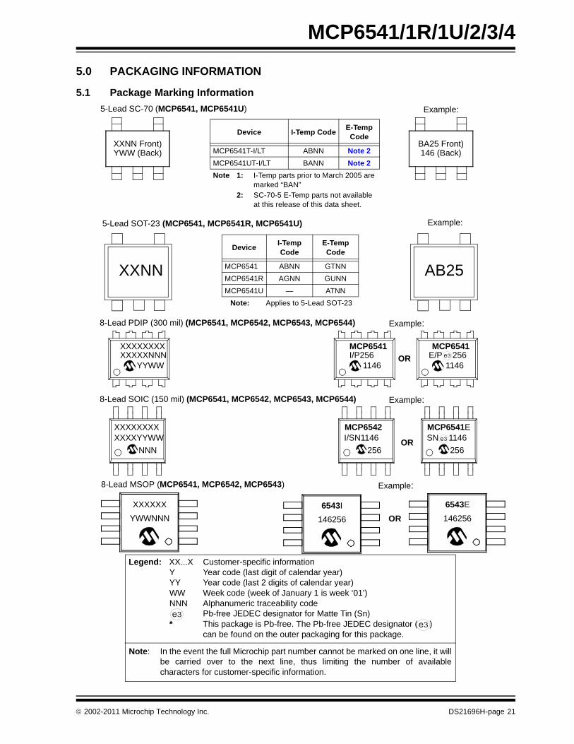
5.0 PACKAGING INFORMATION
5.1 Package Marking Information
XXXXXXXXXXXXXNNN
YYWW
8-Lead PDIP (300 mil) (MCP6541, MCP6542, MCP6543, MCP6544) Example:
8-Lead SOIC (150 mil) (MCP6541, MCP6542, MCP6543, MCP6544) Example:
XXXXXXXXXXXXYYWW
NNN
MCP6541I/P256
1146
MCP6542I/SN1146
256
8-Lead MSOP (MCP6541, MCP6542, MCP6543) Example:
XXXXXXYWWNNN
6543I146256
5-Lead SOT-23 (MCP6541, MCP6541R, MCP6541U) Example:
XXNN AB25
5-Lead SC-70 (MCP6541, MCP6541U) Example:
XXNN Front)YWW (Back)
BA25 Front)146 (Back)
Device I-Temp Code
E-Temp Code
MCP6541 ABNN GTNNMCP6541R AGNN GUNNMCP6541U — ATNN
Note: Applies to 5-Lead SOT-23
Device I-Temp Code E-Temp Code
MCP6541T-I/LT ABNN Note 2MCP6541UT-I/LT BANN Note 2Note 1: I-Temp parts prior to March 2005 are
marked “BAN”2: SC-70-5 E-Temp parts not available
at this release of this data sheet.
Legend: XX...X Customer-specific informationY Year code (last digit of calendar year)YY Year code (last 2 digits of calendar year)WW Week code (week of January 1 is week ‘01’)NNN Alphanumeric traceability code Pb-free JEDEC designator for Matte Tin (Sn)* This package is Pb-free. The Pb-free JEDEC designator ( )
can be found on the outer packaging for this package.
Note: In the event the full Microchip part number cannot be marked on one line, it willbe carried over to the next line, thus limiting the number of availablecharacters for customer-specific information.
3e
3e
MCP6541E/P^^256
1146
MCP6541ESN^^1146
256
OR
OR
3e
3e
6543E146256OR
© 2002-2011 Microchip Technology Inc. DS21696H-page 21

MCP6541/1R/1U/2/3/4
Package Marking Information (Continued)14-Lead PDIP (300 mil) (MCP6544) Example:
14-Lead TSSOP (MCP6544) Example:
XXXXXXXXXXXXXXXXXXXXXXXXXXXX
YYWWNNN
XXXXXXXXYYWWNNN
MCP6544-I/P114656
MCP6544I1146256
MCP6544E/P1146256
OR3e
MCP6544I/P1146256
OR 3e
14-Lead SOIC (150 mil) (MCP6544) Example:
XXXXXXXXXX
YYWWNNNXXXXXXXXXX MCP6544ISL
1146256
MCP6544
1146256I/SL^^
OR
3eOR
MCP6544
1146256E/SL^3̂e
MCP6544E1146256
OR
DS21696H-page 22 © 2002-2011 Microchip Technology Inc.

MCP6541/1R/1U/2/3/4
���������� ��������� �������� ����������������
�������� ����� �� �����!�"��!��#�����$!����!�%�� ����#$ �� ����!�%�� ����#$ �� � ������#��&���!������������� �!���� ����� ��������!�#���������������"�'���(��
)�*+ )� �������� ���� ���#��������&��#�,��$�� �-��-�#�$#�#������ �
����� .�#���� #��$��#����/����!�-��� 0����� �� ���#�����������1��/�����������%���#������#�!��#��##�+22---�����������2���/�����
3��# ��44��" "������� ���4���# ��5 56� ��7
5$�8��%�1�� 5 (1�#�� � ��9(�)�*6,�����:����# � ��;� < ������!�!�1��/���� ���/�� �� ��;� < �����#��!%% �� ���� < ����6,�����=�!#� " ��;� ���� ������!�!�1��/����=�!#� "� ���( ���( ���(6,�����4���#� � ��;� ���� ���(.#�4���#� 4 ���� ���� ���94��!� ���/�� � ���; < ���94��!�=�!#� 8 ���( < ����
D
b
123
E1
E
4 5e e
c
LA1
A A2
������� ������� ��-��� *����9�)
© 2002-2011 Microchip Technology Inc. DS21696H-page 23

MCP6541/1R/1U/2/3/4
����� .�#���� #��$��#����/����!�-��� 0����� �� ���#�����������1��/�����������%���#������#�!��#��##�+22---�����������2���/�����
DS21696H-page 24 © 2002-2011 Microchip Technology Inc.

MCP6541/1R/1U/2/3/4
���������� ��������� �������� ��������������� !�
�������� ����� �� �����!�"��!��#�����$!����!�%�� ����#$ �� ����!�%�� ����#$ �� � ������#��&���!������������� �!���� ����� ��������!�#���������������"�'���(��
)�*+ )� �������� ���� ���#��������&��#�,��$�� �-��-�#�$#�#������ �
����� .�#���� #��$��#����/����!�-��� 0����� �� ���#�����������1��/�����������%���#������#�!��#��##�+22---�����������2���/�����
3��# ��44��" "������� ���4���# ��5 56� ��7
5$�8��%�1�� 5 (4��!�1�#�� � ���(�)�*6$# �!��4��!�1�#�� �� �����)�*6,�����:����# � ���� < ���(��!�!�1��/���� ���/�� �� ��;� < �����#��!%% �� ���� < ���(6,�����=�!#� " ���� < ������!�!�1��/����=�!#� "� ���� < ��;�6,�����4���#� � ���� < ����.#�4���#� 4 ���� < ��9�.#���# 4� ���( < ��;�.#������ � �> < ��>4��!� ���/�� � ���; < ���94��!�=�!#� 8 ���� < ��(�
φ
Nb
E
E1
D
1 2 3
e
e1
A
A1
A2 c
L
L1
������� ������� ��-��� *������)
© 2002-2011 Microchip Technology Inc. DS21696H-page 25

MCP6541/1R/1U/2/3/4
Note: For the most current package drawings, please see the Microchip Packaging Specification located at http://www.microchip.com/packaging
DS21696H-page 26 © 2002-2011 Microchip Technology Inc.

MCP6541/1R/1U/2/3/4
"��������� ��#���$��� ������%�!���� �&��'��#$�
�������� 1�����,� $�����!�&�%��#$������,��0�8$#��$ #�8�����#�!�-�#��#�����#���!������� ?������%����#�*����#�� #����� ����� �� �����!�"��!��#�����$!����!�%�� ����#$ �� ����!�%�� ����#$ �� � ������#��&���!�����@���� �!���� ����� ��������!�#���������������"�'���(��
)�*+�)� �������� ���� ���#��������&��#�,��$�� �-��-�#�$#�#������ �
����� .�#���� #��$��#����/����!�-��� 0����� �� ���#�����������1��/�����������%���#������#�!��#��##�+22---�����������2���/�����
3��# �5*:"������ ���4���# ��5 56� ��7
5$�8��%�1�� 5 ;1�#�� � �����)�* ��#����#����1���� � < < ������!�!�1��/���� ���/�� �� ���( ���� ���()� ��#����#����1���� �� ���( < <��$�!��#���$�!��=�!#� " ���� ���� ���(��!�!�1��/����=�!#� "� ���� ��(� ��;�6,�����4���#� � ���; ��9( ���� ���#����#����1���� 4 ���( ���� ��(�4��!� ���/�� � ���; ���� ���(3����4��!�=�!#� 8� ���� ��9� ����4-��4��!�=�!#� 8 ���� ���; ����6,������-����������? �) < < ����
N
E1
NOTE 1
D
1 2 3
A
A1
A2
L
b1b
e
E
eB
c
������� ������� ��-��� *�����;)
© 2002-2011 Microchip Technology Inc. DS21696H-page 27

MCP6541/1R/1U/2/3/4
Note: For the most current package drawings, please see the Microchip Packaging Specification located at http://www.microchip.com/packaging
DS21696H-page 28 © 2002-2011 Microchip Technology Inc.

MCP6541/1R/1U/2/3/4
Note: For the most current package drawings, please see the Microchip Packaging Specification located at http://www.microchip.com/packaging
© 2002-2011 Microchip Technology Inc. DS21696H-page 29

MCP6541/1R/1U/2/3/4
"��������� ��������� ��������%������()�!*+�����&��'����$��
����� .�#���� #��$��#����/����!�-��� 0����� �� ���#�����������1��/�����������%���#������#�!��#��##�+22---�����������2���/�����
DS21696H-page 30 © 2002-2011 Microchip Technology Inc.

MCP6541/1R/1U/2/3/4
Note: For the most current package drawings, please see the Microchip Packaging Specification located at http://www.microchip.com/packaging
© 2002-2011 Microchip Technology Inc. DS21696H-page 31

MCP6541/1R/1U/2/3/4
Note: For the most current package drawings, please see the Microchip Packaging Specification located at http://www.microchip.com/packaging
DS21696H-page 32 © 2002-2011 Microchip Technology Inc.
MCP6541/1R/1U/2/3/4
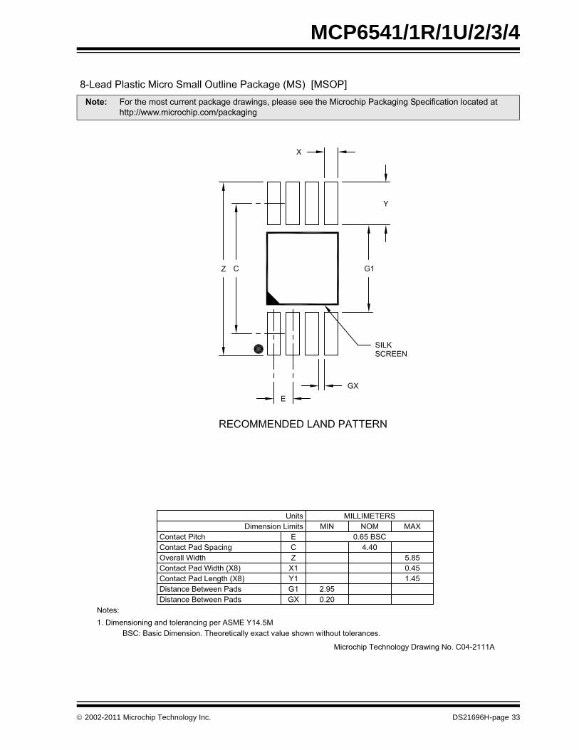
Note: For the most current package drawings, please see the Microchip Packaging Specification located at http://www.microchip.com/packaging
© 2002-2011 Microchip Technology Inc. DS21696H-page 33

MCP6541/1R/1U/2/3/4
,-��������� ��#���$��� ������%�!���� �&��'��#$�
�������� 1�����,� $�����!�&�%��#$������,��0�8$#��$ #�8�����#�!�-�#��#�����#���!������� ?������%����#�*����#�� #����� ����� �� �����!�"��!��#�����$!����!�%�� ����#$ �� ����!�%�� ����#$ �� � ������#��&���!�����@���� �!���� ����� ��������!�#���������������"�'���(��
)�*+�)� �������� ���� ���#��������&��#�,��$�� �-��-�#�$#�#������ �
����� .�#���� #��$��#����/����!�-��� 0����� �� ���#�����������1��/�����������%���#������#�!��#��##�+22---�����������2���/�����
3��# �5*:"������ ���4���# ��5 56� ��7
5$�8��%�1�� 5 ��1�#�� � �����)�* ��#����#����1���� � < < ������!�!�1��/���� ���/�� �� ���( ���� ���()� ��#����#����1���� �� ���( < <��$�!��#���$�!��=�!#� " ���� ���� ���(��!�!�1��/����=�!#� "� ���� ��(� ��;�6,�����4���#� � ���( ��(� ���( ���#����#����1���� 4 ���( ���� ��(�4��!� ���/�� � ���; ���� ���(3����4��!�=�!#� 8� ���( ��9� ����4-��4��!�=�!#� 8 ���� ���; ����6,������-����������? �) < < ����
N
E1
D
NOTE 1
1 2 3
E
c
eB
A2
L
A
A1b1
b e
������� ������� ��-��� *�����()
DS21696H-page 34 © 2002-2011 Microchip Technology Inc.

MCP6541/1R/1U/2/3/4
Note: For the most current package drawings, please see the Microchip Packaging Specification located at http://www.microchip.com/packaging
© 2002-2011 Microchip Technology Inc. DS21696H-page 35

MCP6541/1R/1U/2/3/4
Note: For the most current package drawings, please see the Microchip Packaging Specification located at http://www.microchip.com/packaging
DS21696H-page 36 © 2002-2011 Microchip Technology Inc.

MCP6541/1R/1U/2/3/4
����� .�#���� #��$��#����/����!�-��� 0����� �� ���#�����������1��/�����������%���#������#�!��#��##�+22---�����������2���/�����
© 2002-2011 Microchip Technology Inc. DS21696H-page 37

MCP6541/1R/1U/2/3/4
Note: For the most current package drawings, please see the Microchip Packaging Specification located at http://www.microchip.com/packaging
DS21696H-page 38 © 2002-2011 Microchip Technology Inc.

MCP6541/1R/1U/2/3/4
Note: For the most current package drawings, please see the Microchip Packaging Specification located at http://www.microchip.com/packaging
© 2002-2011 Microchip Technology Inc. DS21696H-page 39

MCP6541/1R/1U/2/3/4
Note: For the most current package drawings, please see the Microchip Packaging Specification located at http://www.microchip.com/packaging
DS21696H-page 40 © 2002-2011 Microchip Technology Inc.
MCP6541/1R/1U/2/3/4
APPENDIX A: REVISION HISTORY
Revision H (December 2011)The following is the list of modifications:
1. Updated Package Types drawings to correctlyshow the device representation for the SC-70package.
1. Updated package’s temperatures in the Temper-ature Characteristics table.
2. Corrected the marking information table for the5-Lead SC-70 package (MCP6541 andMCP6541U) in Section 5.1 “Package MarkingInformation”.
3. Updated package outline drawings inSection 5.1 “Package Marking Information”to show all views for each package.
4. Minor editorial changes.
Revision G (March 2011)The following is the list of modifications:
1. Updated the marking information for the 5-LeadSC-70 package in Section 5.1 “PackageMarking Information”.
Revision F (September 2007)1. Corrected polarity of MCP6541U SOT-23-5 pin
out diagram on front page.2. Section 5.0 “Packaging Information”:
Updated package outline drawings perMarCom.
Revision E (September 2006)The following is the list of modifications:
1. Added MCP6541U pinout for the SOT-23-5package.
2. Clarified Absolute Maximum Analog InputVoltage and Current Specifications.
3. Added applications write-ups on unusedcomparators.
4. Added disclaimer to package outline drawings.
Revision D (May 2006)The following is the list of modifications:
1. Added E-temp parts.2. Changed VHYST temperature specification to
linear and quadratic temperature coefficients.3. Changed specifications and plots for E-Temp.4. Added section 3.0 “Pin Descriptions”.5. Corrected package marking (See Section 5.1
“Package Marking Information”).6. Added Appendix A: “Revision History”.
Revision C (September 2003)• Undocumented changes.
Revision B (November 2002)• Undocumented changes.
Revision A (March 2002)• Original Release of this Document.
© 2002-2011 Microchip Technology Inc. DS21696H-page 41
MCP6541/1R/1U/2/3/4
NOTES:DS21696H-page 42 © 2002-2011 Microchip Technology Inc.

MCP6541/1R/1U/2/3/4
PRODUCT IDENTIFICATION SYSTEMTo order or obtain information, e.g., on pricing or delivery, refer to the factory or the listed sales office.
Device: MCP6541: Single Comparator
MCP6541T: Single Comparator (Tape and Reel)(SC-70, SOT-23, SOIC, MSOP)
MCP6541RT: Single Comparator (Rotated - Tape and Reel) (SOT-23 only)
MCP6541UT: Single Comparator (Tape and Reel)(SC-70, SOT-23; SOT-23-5 is E-Temp only)
MCP6542: Dual ComparatorMCP6542T: Dual Comparator
(Tape and Reel for SOIC and MSOP)MCP6543: Single Comparator with CSMCP6543T: Single Comparator with CS
(Tape and Reel for SOIC and MSOP)MCP6544: Quad ComparatorMCP6544T: Quad Comparator
(Tape and Reel for SOIC and TSSOP)
Temperature Range: I = -40°C to +85°CE * = -40°C to +125°C
* SC-70-5 E-Temp parts not available at this release of the data sheet.
Package: LT = Plastic Package (SC-70), 5-leadOT = Plastic Small Outline Transistor (SOT-23), 5-leadMS = Plastic MSOP, 8-leadP = Plastic DIP (300 mil Body), 8-lead, 14-leadSN = Plastic SOIC (150 mil Body), 8-leadSL = Plastic SOIC (150 mil Body), 14-lead (MCP6544)ST = Plastic TSSOP (4.4mm Body), 14-lead (MCP6544)
PART NO. -X /XX
PackageTemperatureRange
Device
Examples:a) MCP6541T-I/LT: Tape and Reel,
Industrial Temperature, 5LD SC-70.
b) MCP6541T-I/OT: Tape and Reel, Industrial Temperature,5LD SOT-23.
c) MCP6541-I/MS: Tape and Reel, Industrial Temperature,8LD MSOP.
d) MCP6541-E/P: Extended Temperature,8LD PDIP.
e) MCP6541-E/SN: Extended Temperature,8LD SOIC.
f) MCP6541RT-I/OT: Tape and Reel, Industrial Temperature,5LD SOT23.
g) MCP6541UT-E/LT: Tape and Reel, Industrial Temperature,5LD SC-70
h) MCP6541UT-E/OT: Tape and Reel, Extended Temperature,5LD SOT23.
a) MCP6542-I/MS: Industrial Temperature,8LD MSOP.
b) MCP6542T-I/MS: Tape and Reel,Industrial Temperature, 8LD MSOP.
c) MCP6542-I/P: Industrial Temperature, 8LD PDIP.
d) MCP6542-E/SN: Extended Temperature,8LD SOIC.
a) MCP6543-I/SN: Industrial Temperature,8LD SOIC.
b) MCP6543T-I/SN: Tape and Reel,Industrial Temperature, 8LD SOIC.
c) MCP6543-I/P: Industrial Temperature,8LD PDIP.
d) MCP6543-E/SN: Extended Temperature,8LD SOIC.
a) MCP6544T-I/SL: Tape and Reel,Industrial Temperature,14LD SOIC.
b) MCP6544T-E/SL: Tape and Reel,Extended Temperature,14LD SOIC.
c) MCP6544-I/P: Industrial Temperature,14LD PDIP.
d) MCP6544T-E/ST: Tape and Reel,Extended Temperature,14LD TSSOP.
© 2002-2011 Microchip Technology Inc. DS21696H-page 43

MCP6541/1R/1U/2/3/4
NOTES:DS21696H-page 44 © 2002-2011 Microchip Technology Inc.
Note the following details of the code protection feature on Microchip devices:• Microchip products meet the specification contained in their particular Microchip Data Sheet.
• Microchip believes that its family of products is one of the most secure families of its kind on the market today, when used in the intended manner and under normal conditions.
• There are dishonest and possibly illegal methods used to breach the code protection feature. All of these methods, to our knowledge, require using the Microchip products in a manner outside the operating specifications contained in Microchip’s Data Sheets. Most likely, the person doing so is engaged in theft of intellectual property.
• Microchip is willing to work with the customer who is concerned about the integrity of their code.
• Neither Microchip nor any other semiconductor manufacturer can guarantee the security of their code. Code protection does not mean that we are guaranteeing the product as “unbreakable.”
Code protection is constantly evolving. We at Microchip are committed to continuously improving the code protection features of ourproducts. Attempts to break Microchip’s code protection feature may be a violation of the Digital Millennium Copyright Act. If such actsallow unauthorized access to your software or other copyrighted work, you may have a right to sue for relief under that Act.
Information contained in this publication regarding deviceapplications and the like is provided only for your convenienceand may be superseded by updates. It is your responsibility toensure that your application meets with your specifications.MICROCHIP MAKES NO REPRESENTATIONS ORWARRANTIES OF ANY KIND WHETHER EXPRESS ORIMPLIED, WRITTEN OR ORAL, STATUTORY OROTHERWISE, RELATED TO THE INFORMATION,INCLUDING BUT NOT LIMITED TO ITS CONDITION,QUALITY, PERFORMANCE, MERCHANTABILITY ORFITNESS FOR PURPOSE. Microchip disclaims all liabilityarising from this information and its use. Use of Microchipdevices in life support and/or safety applications is entirely atthe buyer’s risk, and the buyer agrees to defend, indemnify andhold harmless Microchip from any and all damages, claims,suits, or expenses resulting from such use. No licenses areconveyed, implicitly or otherwise, under any Microchipintellectual property rights.
© 2002-2011 Microchip Technology Inc.
Trademarks
The Microchip name and logo, the Microchip logo, dsPIC, KEELOQ, KEELOQ logo, MPLAB, PIC, PICmicro, PICSTART, PIC32 logo, rfPIC and UNI/O are registered trademarks of Microchip Technology Incorporated in the U.S.A. and other countries.
FilterLab, Hampshire, HI-TECH C, Linear Active Thermistor, MXDEV, MXLAB, SEEVAL and The Embedded Control Solutions Company are registered trademarks of Microchip Technology Incorporated in the U.S.A.
Analog-for-the-Digital Age, Application Maestro, chipKIT, chipKIT logo, CodeGuard, dsPICDEM, dsPICDEM.net, dsPICworks, dsSPEAK, ECAN, ECONOMONITOR, FanSense, HI-TIDE, In-Circuit Serial Programming, ICSP, Mindi, MiWi, MPASM, MPLAB Certified logo, MPLIB, MPLINK, mTouch, Omniscient Code Generation, PICC, PICC-18, PICDEM, PICDEM.net, PICkit, PICtail, REAL ICE, rfLAB, Select Mode, Total Endurance, TSHARC, UniWinDriver, WiperLock and ZENA are trademarks of Microchip Technology Incorporated in the U.S.A. and other countries.
SQTP is a service mark of Microchip Technology Incorporated in the U.S.A.
All other trademarks mentioned herein are property of their respective companies.
© 2002-2011, Microchip Technology Incorporated, Printed in the U.S.A., All Rights Reserved.
Printed on recycled paper.
ISBN: 978-1-61341-921-2
DS21696H-page 45
Microchip received ISO/TS-16949:2009 certification for its worldwide headquarters, design and wafer fabrication facilities in Chandler and Tempe, Arizona; Gresham, Oregon and design centers in California and India. The Company’s quality system processes and procedures are for its PIC® MCUs and dsPIC® DSCs, KEELOQ® code hopping devices, Serial EEPROMs, microperipherals, nonvolatile memory and analog products. In addition, Microchip’s quality system for the design and manufacture of development systems is ISO 9001:2000 certified.

DS21696H-page 46 © 2002-2011 Microchip Technology Inc.
AMERICASCorporate Office2355 West Chandler Blvd.Chandler, AZ 85224-6199Tel: 480-792-7200 Fax: 480-792-7277Technical Support: http://www.microchip.com/supportWeb Address: www.microchip.comAtlantaDuluth, GA Tel: 678-957-9614 Fax: 678-957-1455BostonWestborough, MA Tel: 774-760-0087 Fax: 774-760-0088ChicagoItasca, IL Tel: 630-285-0071 Fax: 630-285-0075ClevelandIndependence, OH Tel: 216-447-0464 Fax: 216-447-0643DallasAddison, TX Tel: 972-818-7423 Fax: 972-818-2924DetroitFarmington Hills, MI Tel: 248-538-2250Fax: 248-538-2260IndianapolisNoblesville, IN Tel: 317-773-8323Fax: 317-773-5453Los AngelesMission Viejo, CA Tel: 949-462-9523 Fax: 949-462-9608Santa ClaraSanta Clara, CA Tel: 408-961-6444Fax: 408-961-6445TorontoMississauga, Ontario, CanadaTel: 905-673-0699 Fax: 905-673-6509
ASIA/PACIFICAsia Pacific OfficeSuites 3707-14, 37th FloorTower 6, The GatewayHarbour City, KowloonHong KongTel: 852-2401-1200Fax: 852-2401-3431Australia - SydneyTel: 61-2-9868-6733Fax: 61-2-9868-6755China - BeijingTel: 86-10-8569-7000 Fax: 86-10-8528-2104China - ChengduTel: 86-28-8665-5511Fax: 86-28-8665-7889China - ChongqingTel: 86-23-8980-9588Fax: 86-23-8980-9500China - HangzhouTel: 86-571-2819-3187 Fax: 86-571-2819-3189China - Hong Kong SARTel: 852-2401-1200 Fax: 852-2401-3431China - NanjingTel: 86-25-8473-2460Fax: 86-25-8473-2470China - QingdaoTel: 86-532-8502-7355Fax: 86-532-8502-7205China - ShanghaiTel: 86-21-5407-5533 Fax: 86-21-5407-5066China - ShenyangTel: 86-24-2334-2829Fax: 86-24-2334-2393China - ShenzhenTel: 86-755-8203-2660 Fax: 86-755-8203-1760China - WuhanTel: 86-27-5980-5300Fax: 86-27-5980-5118China - XianTel: 86-29-8833-7252Fax: 86-29-8833-7256China - XiamenTel: 86-592-2388138 Fax: 86-592-2388130China - ZhuhaiTel: 86-756-3210040 Fax: 86-756-3210049
ASIA/PACIFICIndia - BangaloreTel: 91-80-3090-4444 Fax: 91-80-3090-4123India - New DelhiTel: 91-11-4160-8631Fax: 91-11-4160-8632India - PuneTel: 91-20-2566-1512Fax: 91-20-2566-1513Japan - OsakaTel: 81-66-152-7160 Fax: 81-66-152-9310Japan - YokohamaTel: 81-45-471- 6166 Fax: 81-45-471-6122Korea - DaeguTel: 82-53-744-4301Fax: 82-53-744-4302Korea - SeoulTel: 82-2-554-7200Fax: 82-2-558-5932 or 82-2-558-5934Malaysia - Kuala LumpurTel: 60-3-6201-9857Fax: 60-3-6201-9859Malaysia - PenangTel: 60-4-227-8870Fax: 60-4-227-4068Philippines - ManilaTel: 63-2-634-9065Fax: 63-2-634-9069SingaporeTel: 65-6334-8870Fax: 65-6334-8850Taiwan - Hsin ChuTel: 886-3-5778-366Fax: 886-3-5770-955Taiwan - KaohsiungTel: 886-7-536-4818Fax: 886-7-330-9305Taiwan - TaipeiTel: 886-2-2500-6610 Fax: 886-2-2508-0102Thailand - BangkokTel: 66-2-694-1351Fax: 66-2-694-1350
EUROPEAustria - WelsTel: 43-7242-2244-39Fax: 43-7242-2244-393Denmark - CopenhagenTel: 45-4450-2828 Fax: 45-4485-2829France - ParisTel: 33-1-69-53-63-20 Fax: 33-1-69-30-90-79Germany - MunichTel: 49-89-627-144-0 Fax: 49-89-627-144-44Italy - Milan Tel: 39-0331-742611 Fax: 39-0331-466781Netherlands - DrunenTel: 31-416-690399 Fax: 31-416-690340Spain - MadridTel: 34-91-708-08-90Fax: 34-91-708-08-91UK - WokinghamTel: 44-118-921-5869Fax: 44-118-921-5820
Worldwide Sales and Service
11/29/11