MCP6041 - 600nA, Rail-to-Rail Input/Output Op...
48
2019 Microchip Technology Inc. DS20001669E-page 1 MCP6041/2/3/4 Features • Low Quiescent Current: 600 nA/amplifier (typical) • Rail-to-Rail Input/Output • Gain Bandwidth Product: 14 kHz (typical) • Wide Supply Voltage Range: 1.4V to 6.0V • Unity Gain Stable • Available in Single, Dual, and Quad • Chip Select (CS ) with MCP6043 • Available in 5-lead and 6-lead SOT-23 Packages • Temperature Ranges: - Industrial: -40°C to +85°C - Extended: -40°C to +125°C Applications • Toll Booth Tags • Wearable Products • Temperature Measurement • Battery Powered Design Aids • SPICE Macro Models • FilterLab ® Software • MAPS (Microchip Advanced Part Selector) • Analog Demonstration and Evaluation Boards • Application Notes Related Devices • MCP6141/2/3/4: G = +10 Stable Op Amps Typical Application Description The MCP6041/2/3/4 family of operational amplifiers (op amps) from Microchip Technology Inc. operate with a single supply voltage as low as 1.4V, while drawing less than 1 μA (maximum) of quiescent current per amplifier. These devices are also designed to support rail-to-rail input and output operation. This combination of features supports battery-powered and portable applications. The MCP6041/2/3/4 amplifiers have a gain-bandwidth product of 14 kHz (typical) and are unity gain stable. These specifications make these op amps appropriate for low frequency applications, such as battery current monitoring and sensor conditioning. The MCP6041/2/3/4 family operational amplifiers are offered in single (MCP6041), single with Chip Select (CS ) (MCP6043), dual (MCP6042), and quad (MCP6044) configurations. The MCP6041 device is available in the 5-lead SOT-23 package, and the MCP6043 device is available in the 6-lead SOT-23 package. Package Types V DD I DD MCP604X 100 k 1M 1.4V V OUT High Side Battery Current Sensor 10 to 6.0V I DD V DD V OUT – 10 V/V 10 ----------------------------------------- = + – V IN + V IN – V SS V DD V OUT 1 2 3 4 8 7 6 5 NC NC NC MCP6041 PDIP, SOIC, MSOP MCP6042 PDIP, SOIC, MSOP MCP6043 PDIP, SOIC, MSOP MCP6044 PDIP, SOIC, TSSOP V INA + V INA – V SS V OUTB V INB – 1 2 3 4 8 7 6 5 V INB + V DD V OUTA V IN + V IN – V SS V DD V OUT 1 2 3 4 8 7 6 5 NC CS NC V INA + V INA – V DD V IND – V IND + 1 2 3 4 14 13 12 11 V SS V OUTD V OUTA V INB – V INB + V OUTB V INC + V INC – 5 6 7 10 9 8 V OUTC V IN + V SS V IN – 1 2 3 5 4 V DD V OUT MCP6041 SOT-23-5 V IN + V SS V IN – 1 2 3 6 4 V DD V OUT MCP6043 SOT-23-6 5 CS 600 nA, Rail-to-Rail Input/Output Op Amps
Transcript of MCP6041 - 600nA, Rail-to-Rail Input/Output Op...

MCP6041/2/3/4600 nA, Rail-to-Rail Input/Output Op Amps
Features
• Low Quiescent Current: 600 nA/amplifier (typical)
• Rail-to-Rail Input/Output
• Gain Bandwidth Product: 14 kHz (typical)
• Wide Supply Voltage Range: 1.4V to 6.0V
• Unity Gain Stable
• Available in Single, Dual, and Quad
• Chip Select (CS) with MCP6043
• Available in 5-lead and 6-lead SOT-23 Packages
• Temperature Ranges:
- Industrial: -40°C to +85°C
- Extended: -40°C to +125°C
Applications
• Toll Booth Tags
• Wearable Products
• Temperature Measurement
• Battery Powered
Design Aids
• SPICE Macro Models
• FilterLab® Software
• MAPS (Microchip Advanced Part Selector)
• Analog Demonstration and Evaluation Boards
• Application Notes
Related Devices
• MCP6141/2/3/4: G = +10 Stable Op Amps
Typical Application
Description
The MCP6041/2/3/4 family of operational amplifiers(op amps) from Microchip Technology Inc. operate witha single supply voltage as low as 1.4V, while drawingless than 1 µA (maximum) of quiescent current peramplifier. These devices are also designed to supportrail-to-rail input and output operation. This combinationof features supports battery-powered and portableapplications.
The MCP6041/2/3/4 amplifiers have a gain-bandwidthproduct of 14 kHz (typical) and are unity gain stable.These specifications make these op amps appropriatefor low frequency applications, such as battery currentmonitoring and sensor conditioning.
The MCP6041/2/3/4 family operational amplifiers areoffered in single (MCP6041), single with Chip Select(CS) (MCP6043), dual (MCP6042), and quad(MCP6044) configurations. The MCP6041 device isavailable in the 5-lead SOT-23 package, and theMCP6043 device is available in the 6-lead SOT-23package.
Package Types
VDDIDD
MCP604X100 k
1 M
1.4V
VOUT
High Side Battery Current Sensor
10to6.0V
IDD
VDD VOUT–10 V/V 10
------------------------------------------=
+
–
VIN+
VIN–
VSS
VDD
VOUT
1
2
3
4
8
7
6
5 NC
NCNC
MCP6041PDIP, SOIC, MSOP
MCP6042PDIP, SOIC, MSOP
MCP6043PDIP, SOIC, MSOP
MCP6044PDIP, SOIC, TSSOP
VINA+
VINA–
VSS
VOUTB
VINB–
1
2
3
4
8
7
6
5 VINB+
VDDVOUTA
VIN+
VIN–
VSS
VDD
VOUT
1
2
3
4
8
7
6
5 NC
CSNC
VINA+
VINA–
VDD
VIND–
VIND+
1
23
4
14
13
12
11 VSS
VOUTDVOUTA
VINB–
VINB+
VOUTB
VINC+
VINC–
56
7
10
9
8 VOUTC
VIN+
VSS
VIN–
1
2
3
5
4
VDDVOUT
MCP6041SOT-23-5
VIN+
VSS
VIN–
12
3
6
4
VDDVOUT
MCP6043SOT-23-6
5 CS
2019 Microchip Technology Inc. DS20001669E-page 1

MCP6041/2/3/4
1.0 ELECTRICAL CHARACTERISTICS
Absolute Maximum Ratings †
VDD – VSS ........................................................................7.0VCurrent at Input Pins .....................................................±2 mAAnalog Inputs (VIN+, VIN–) ............. VSS – 1.0V to VDD + 1.0VAll Other Inputs and Outputs.......... VSS – 0.3V to VDD + 0.3VDifference Input voltage ...................................... |VDD – VSS|Output Short Circuit Current ..................................continuousCurrent at Output and Supply Pins ............................±30 mAStorage Temperature....................................–65°C to +150°CJunction Temperature..................................................+150°CESD protection on all pins (HBM; MM) 4 kV; 200V
† Notice: Stresses above those listed under “AbsoluteMaximum Ratings” may cause permanent damage to thedevice. This is a stress rating only and functional operation ofthe device at those or any other conditions above thoseindicated in the operational listings of this specification is notimplied. Exposure to maximum rating conditions for extendedperiods may affect device reliability.
†† See Section 4.1 “Rail-to-Rail Input”
DC ELECTRICAL CHARACTERISTICS
Electrical Characteristics: Unless otherwise indicated, VDD = +1.4V to +5.5V, VSS = GND, TA = 25°C, VCM = VDD/2,VOUT VDD/2, VL = VDD/2, and RL = 1 Mto VL (refer to Figure 1-2 and Figure 1-3).
Parameters Sym Min Typ Max Units Conditions
Input Offset
Input Offset Voltage VOS -3 — +3 mV VCM = VSS
Drift with Temperature VOS/TA — ±2 — µV/°C VCM = VSS, TA= -40°C to +85°C
VOS/TA — ±15 — µV/°C VCM = VSS, TA= +85°C to +125°C
Power Supply Rejection PSRR 70 85 — dB VCM = VSS
Input Bias Current and Impedance
Input Bias Current IB — 1 — pA
Industrial Temperature IB — 20 100 pA TA = +85°
Extended Temperature IB — 1200 5000 pA TA = +125°
Input Offset Current IOS — 1 — pA
Common-mode Input Impedance ZCM — 1013||6 — ||pF
Differential Input Impedance ZDIFF — 1013||6 — ||pF
Common-mode
Common-mode Input Range VCMR VSS0.3 — VDD+0.3 V
Common-mode Rejection Ratio CMRR 62 80 — dB VDD = 5V, VCM = -0.3V to 5.3V
CMRR 60 75 — dB VDD = 5V, VCM = 2.5V to 5.3V
CMRR 60 80 — dB VDD = 5V, VCM = -0.3V to 2.5V
Open-Loop Gain
DC Open-Loop Gain (large signal) AOL 95 115 — dB RL = 50 k to VL, VOUT = 0.1V to VDD0.1V
Output
Maximum Output Voltage Swing VOL, VOH VSS + 10 — VDD 10 mV RL = 50 k to VL, 0.5V input overdrive
Linear Region Output Voltage Swing VOVR VSS + 100 — VDD 100 mV RL = 50 k to VL,AOL 95 dB
Output Short Circuit Current ISC — 2 — mA VDD = 1.4V
ISC — 20 — mA VDD = 5.5V
Power Supply
Supply Voltage VDD 1.4 — 6.0 V (Note 1)
Quiescent Current per Amplifier IQ 0.3 0.6 1.0 µA IO = 0
Note 1: All parts with date codes November 2007 and later have been screened to ensure operation at VDD = 6.0V. However,the other minimum and maximum specifications are measured at 1.4V and/or 5.5V.
DS20001669E-page 2 2019 Microchip Technology Inc.
MCP6041/2/3/4
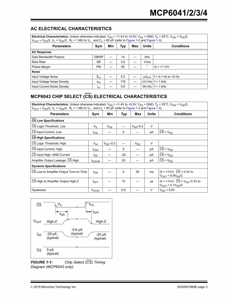
AC ELECTRICAL CHARACTERISTICS
MCP6043 CHIP SELECT (CS) ELECTRICAL CHARACTERISTICS
FIGURE 1-1: Chip Select (CS) Timing Diagram (MCP6043 only).
Electrical Characteristics: Unless otherwise indicated, VDD = +1.4V to +5.5V, VSS = GND, TA = 25°C, VCM = VDD/2,VOUT VDD/2, VL = VDD/2, RL = 1 Mto VL, and CL = 60 pF (refer to Figure 1-2 and Figure 1-3).
Parameters Sym Min Typ Max Units Conditions
AC Response
Gain Bandwidth Product GBWP — 14 — kHz
Slew Rate SR — 3.0 — V/ms
Phase Margin PM — 65 — ° G = +1 V/V
Noise
Input Voltage Noise Eni — 5.0 — µVP-P f = 0.1 Hz to 10 Hz
Input Voltage Noise Density eni — 170 — nV/Hz f = 1 kHz
Input Current Noise Density ini — 0.6 — fA/Hz f = 1 kHz
Electrical Characteristics: Unless otherwise indicated, VDD = +1.4V to +5.5V, VSS = GND, TA = 25°C, VCM = VDD/2,VOUT VDD/2, VL = VDD/2, RL = 1 Mto VL, and CL = 60 pF (refer to Figure 1-2 and Figure 1-3).
Parameters Sym Min Typ Max Units Conditions
CS Low Specifications
CS Logic Threshold, Low VIL VSS — VSS+0.3 V
CS Input Current, Low ICSL — 5 — pA CS = VSS
CS High Specifications
CS Logic Threshold, High VIH VDD–0.3 — VDD V
CS Input Current, High ICSH — 5 — pA CS = VDD
CS Input High, GND Current ISS — -20 — pA CS = VDD
Amplifier Output Leakage, CS High IOLEAK — 20 — pA CS = VDD
Dynamic Specifications
CS Low to Amplifier Output Turn-on Time tON — 2 50 ms G = +1V/V, CS = 0.3V toVOUT = 0.9VDD/2
CS High to Amplifier Output High-Z tOFF — 10 — µs G = +1V/V, CS = VDD–0.3V to VOUT = 0.1VDD/2
Hysteresis VHYST — 0.6 — V VDD = 5.0V
VIL
High-Z
tON
VIHCS
tOFF
VOUT
-20 pA
High-Z
ISS
ICS 5 pA
-20 pA
-0.6 µA
(typical) (typical)
(typical)
(typical)
2019 Microchip Technology Inc. DS20001669E-page 3

MCP6041/2/3/4
TEMPERATURE CHARACTERISTICS
1.1 Test Circuits
The test circuits used for the DC and AC tests areshown in Figure 1-2 and Figure 1-3. The bypasscapacitors are laid out according to the rules discussedin Section 4.6 “Supply Bypass”.
FIGURE 1-2: AC and DC Test Circuit for Most Non-Inverting Gain Conditions.
FIGURE 1-3: AC and DC Test Circuit for Most Inverting Gain Conditions.
Electrical Characteristics: Unless otherwise indicated, VDD = +1.4V to +5.5V, VSS = GND.
Parameters Sym Min Typ Max Units Conditions
Temperature Ranges
Specified Temperature Range TA -40 — +85 °C Industrial Temperature parts
TA -40 — +125 °C Extended Temperature parts
Operating Temperature Range TA -40 — +125 °C (Note 1)
Storage Temperature Range TA -65 — +150 °C
Thermal Package Resistances
Thermal Resistance, 5L-SOT-23 JA — 256 — °C/W
Thermal Resistance, 6L-SOT-23 JA — 230 — °C/W
Thermal Resistance, 8L-PDIP JA — 85 — °C/W
Thermal Resistance, 8L-SOIC JA — 163 — °C/W
Thermal Resistance, 8L-MSOP JA — 206 — °C/W
Thermal Resistance, 14L-PDIP JA — 70 — °C/W
Thermal Resistance, 14L-SOIC JA — 120 — °C/W
Thermal Resistance, 14L-TSSOP JA — 100 — °C/W
Note 1: The MCP6041/2/3/4 family of Industrial Temperature op amps operates over this extended range, but with reduced performance. In any case, the internal Junction Temperature (TJ) must not exceed the Absolute Maximum specification of +150°C.
VDD
MCP604X
RG RF
RNVOUT
VIN
VDD/2
1 µF
CL RL
VL
0.1 µF
VDD
MCP604X
RG RF
RNVOUT
VDD/2
VIN
1 µF
CL RL
VL
0.1 µF
DS20001669E-page 4 2019 Microchip Technology Inc.

MCP6041/2/3/4
2.0 TYPICAL PERFORMANCE CURVES
Note: Unless otherwise indicated, TA = +25°C, VDD = +1.4V to +6.0V, VSS = GND, VCM = VDD/2, VOUT VDD/2, VL = VDD/2, RL = 1 M to VL, and CL = 60 pF.
FIGURE 2-1: Input Offset Voltage.
FIGURE 2-2: Input Offset Voltage Drift with TA = -40°C to +85°C.
FIGURE 2-3: Input Offset Voltage vs. Common-mode Input Voltage with VDD = 1.4V.
FIGURE 2-4: Input Offset Voltage Drift with TA = +85°C to +125°C and VDD = 1.4V.
FIGURE 2-5: Input Offset Voltage Drift with TA = +25°C to +125°C and VDD = 5.5V.
FIGURE 2-6: Input Offset Voltage vs. Common-mode Input Voltage with VDD = 5.5V.
Note: The graphs and tables provided following this note are a statistical summary based on a limited number ofsamples and are provided for informational purposes only. The performance characteristics listed herein arenot tested or guaranteed. In some graphs or tables, the data presented may be outside the specifiedoperating range (e.g., outside specified power supply range) and therefore outside the warranted range.
0%
1%
2%
3%
4%
5%
6%
7%
8%
9%
10%
-3 -2 -1 0 1 2 3Input Offset Voltage (mV)
Per
cen
tag
e o
f O
ccu
rre
nc
es
1124 SamplesVDD = 1.4V and 5.5VVCM = VSS
0%1%2%3%4%5%6%7%8%9%
10%11%12%
-10 -8 -6 -4 -2 0 2 4 6 8 10Input Offset Voltage Drift (µV/°C)
Per
cen
tag
e o
f O
ccu
rre
nc
es
1124 SamplesTA = -40°C to +85°CVDD = 1.4VVCM = VSS
-2000
-1500
-1000
-500
0
500
1000
1500
2000
-0.4
-0.2 0.0
0.2
0.4
0.6
0.8
1.0
1.2
1.4
1.6
1.8
Common Mode Input Voltage (V)
Inp
ut
Off
set
Vo
ltag
e (µ
V) VDD = 1.4V
Representative Part
TA = +125°CTA = +85°CTA = +25°CTA = -40°C
0%
2%
4%
6%
8%
10%
12%
14%
16%
18%
-32 -28 -24 -20 -16 -12 -8 -4 0 4Input Offset Voltage Drift (µV/°C)
Per
cen
tag
e o
f O
ccu
rren
ces
245 Samples1 Representative LotTA = +85°C to +125°CVDD = 1.4VVCM = VSS
0%2%4%6%8%
10%12%14%16%18%20%22%24%
-32 -28 -24 -20 -16 -12 -8 -4 0 4Input Offset Voltage Drift (µV/°C)
Per
cen
tag
e o
f O
ccu
rren
ces
239 Samples1 Representative LotTA = +85°C to +125°CVDD = 5.5VVCM = VSS
-2000
-1500
-1000
-500
0
500
1000
1500
2000
-0.5 0.0
0.5
1.0
1.5
2.0
2.5
3.0
3.5
4.0
4.5
5.0
5.5
6.0
Common Mode Input Voltage (V)
Inp
ut
Off
set
Vo
ltag
e (µ
V) VDD = 5.5V
Representative Part
TA = +125°CTA = +85°CTA = +25°CTA = -40°C
2019 Microchip Technology Inc. DS20001669E-page 5

MCP6041/2/3/4
Note: Unless otherwise indicated, TA = +25°C, VDD = +1.4V to +6.0V, VSS = GND, VCM = VDD/2, VOUT VDD/2, VL = VDD/2, RL = 1 M to VL, and CL = 60 pF.
FIGURE 2-7: Input Offset Voltage vs. Output Voltage.
FIGURE 2-8: Input Noise Voltage Density vs. Frequency.
FIGURE 2-9: CMRR, PSRR vs. Frequency.
FIGURE 2-10: The MCP6041/2/3/4 family shows no phase reversal.
FIGURE 2-11: Input Noise Voltage Density vs. Common-mode Input Voltage.
FIGURE 2-12: CMRR, PSRR vs. Ambient Temperature.
250
300
350
400
450
500
0.0 0.5 1.0 1.5 2.0 2.5 3.0 3.5 4.0 4.5 5.0 5.5Output Voltage (V)
Inp
ut
Off
set
Vo
ltag
e (µ
V)
VDD = 5.5V
VDD = 1.4V
100
1000
0.1 1 10 100 1000Frequency (Hz)
Inpu
t Noi
se V
olta
ge D
ensi
ty(n
V/H
z)
20
30
40
50
60
70
80
90
0.1 1 10 100 1000Frequency (Hz)
CM
RR
, PS
RR
(d
B)
PSRR–PSRR+CMRR
Referred to Input
-1
0
1
2
3
4
5
6
0 5 10 15 20 25Time (5 ms/div)
Inp
ut,
Ou
tpu
t V
olt
ages
(V
)
VIN
VDD = 5.0VG = +2 V/V
VOUT
0
50
100
150
200
250
300
-0.5 0.0
0.5
1.0
1.5
2.0
2.5
3.0
3.5
4.0
4.5
5.0
5.5
Common Mode Input Voltage (V)
Inpu
t Noi
se V
olta
ge D
ensi
ty(n
V/H
z)
f = 1 kHzVDD = 5.0V
70
75
80
85
90
95
100
-50 -25 0 25 50 75 100 125Ambient Temperature (°C)
PS
RR
, C
MR
R (
dB
)
PSRR(VCM = VSS)
CMRR(VDD = 5.0V, VCM = -0.3V to +5.3V)
DS20001669E-page 6 2019 Microchip Technology Inc.
MCP6041/2/3/4
Note: Unless otherwise indicated, TA = +25°C, VDD = +1.4V to +6.0V, VSS = GND, VCM = VDD/2, VOUT VDD/2, VL = VDD/2, RL = 1 M to VL, and CL = 60 pF.
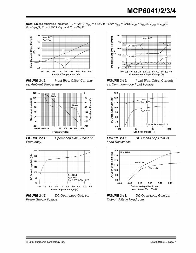
FIGURE 2-13: Input Bias, Offset Currents vs. Ambient Temperature.
FIGURE 2-14: Open-Loop Gain, Phase vs. Frequency.
FIGURE 2-15: DC Open-Loop Gain vs. Power Supply Voltage.
FIGURE 2-16: Input Bias, Offset Currents vs. Common-mode Input Voltage.
FIGURE 2-17: DC Open-Loop Gain vs. Load Resistance.
FIGURE 2-18: DC Open-Loop Gain vs. Output Voltage Headroom.
0.1
1
10
100
1000
10000
45 55 65 75 85 95 105 115 125Ambient Temperature (°C)
Inp
ut
Bia
s an
d O
ffs
et C
urr
ents
(pA
)
| IOS |
IB
VDD = 5.5VVCM = VDD
0.1
1
10
100
1k
10k
-20
0
20
40
60
80
100
120
1.E-03
1.E-02
1.E-01
1.E+00
1.E+01
1.E+02
1.E+03
1.E+04
1.E+05Frequency (Hz)
Op
en-L
oo
p G
ain
(d
B)
-210
-180
-150
-120
-90
-60
-30
0
Op
en-L
oo
p P
has
e (
°)
0.001 0.01 0.1 1 10 100 1k 10k 100k
Gain
Phase
80
90
100
110
120
130
140
1.0 1.5 2.0 2.5 3.0 3.5 4.0 4.5 5.0 5.5Power Supply Voltage (V)
DC
Op
en
-Lo
op
Ga
in (
dB
)
RL = 50 kΩVDD = 5.0VVOUT = 0.1V to VDD - 0.1V
0.1
1
10
100
1000
10000
0.0 0.5 1.0 1.5 2.0 2.5 3.0 3.5 4.0 4.5 5.0 5.5Common Mode Input Voltage (V)
Inp
ut
Bia
s an
d O
ffse
t C
urr
ents
(pA
)
VDD = 5.5V
| IOS |
IB
0.1
1
10
100
1k
10k
TA = +125°C
TA = +85°C
60
70
80
90
100
110
120
130
1.E+02 1.E+03 1.E+04 1.E+05Load Resistance ( )
DC
Ope
n-Lo
op G
ain
(dB
)VDD = 1.4V
100 1k 10k 100k
VOUT = 0.1V to VDD – 0.1V
VDD = 5.5V
80
90
100
110
120
130
140
0.00 0.05 0.10 0.15 0.20 0.25Output Voltage Headroom; VDD – VOH or VOL – VSS (V)
DC
Ope
n-Lo
op G
ain
(dB
) RL = 50 k
VDD = 5.5V
VDD = 1.4V
2019 Microchip Technology Inc. DS20001669E-page 7
MCP6041/2/3/4
Note: Unless otherwise indicated, TA = +25°C, VDD = +1.4V to +6.0V, VSS = GND, VCM = VDD/2, VOUT VDD/2, VL = VDD/2, RL = 1 M to VL, and CL = 60 pF.
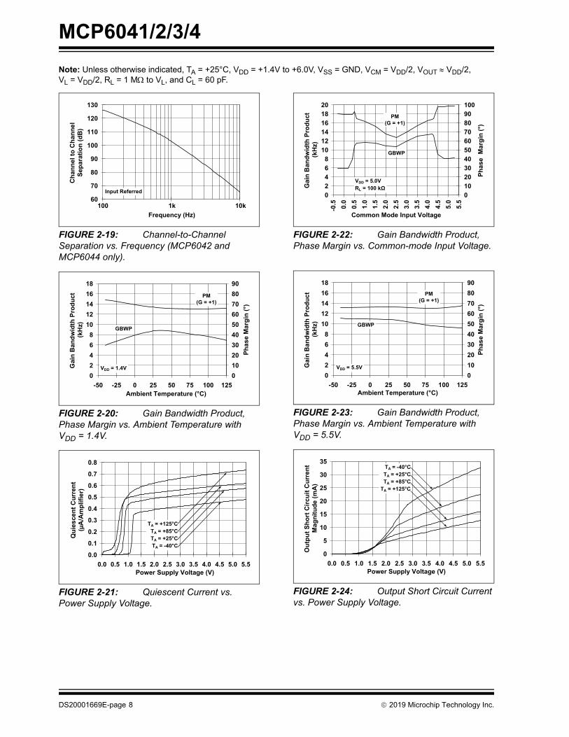
FIGURE 2-19: Channel-to-Channel Separation vs. Frequency (MCP6042 and MCP6044 only).
FIGURE 2-20: Gain Bandwidth Product, Phase Margin vs. Ambient Temperature with VDD = 1.4V.
FIGURE 2-21: Quiescent Current vs. Power Supply Voltage.
FIGURE 2-22: Gain Bandwidth Product, Phase Margin vs. Common-mode Input Voltage.
FIGURE 2-23: Gain Bandwidth Product, Phase Margin vs. Ambient Temperature with VDD = 5.5V.
FIGURE 2-24: Output Short Circuit Current vs. Power Supply Voltage.
60
70
80
90
100
110
120
130
1.E+02 1.E+03 1.E+04Frequency (Hz)
Ch
an
nel
to
Ch
ann
el
Sep
arat
ion
(d
B)
100 1k 10k
Input Referred
0
2
4
6
8
10
12
14
16
18
-50 -25 0 25 50 75 100 125Ambient Temperature (°C)
Gai
n B
and
wid
th P
rod
uct
(kH
z)
0
10
20
30
40
50
60
70
80
90
Ph
ase
Ma
rgin
(°)
PM(G = +1)
GBWP
VDD = 1.4V
0.0
0.1
0.2
0.3
0.4
0.5
0.6
0.7
0.8
0.0 0.5 1.0 1.5 2.0 2.5 3.0 3.5 4.0 4.5 5.0 5.5Power Supply Voltage (V)
Qu
ies
cen
t C
urr
ent
(µA
/Am
pli
fier
)
TA = +125°CTA = +85°CTA = +25°CTA = -40°C
0
246
810
121416
1820
-0.5 0.0
0.5
1.0
1.5
2.0
2.5
3.0
3.5
4.0
4.5
5.0
5.5
Common Mode Input Voltage
Gai
n B
and
wid
th P
rod
uct
(kH
z)
0
102030
4050
607080
90100
Ph
ase
Ma
rgin
(°)
PM(G = +1)
GBWP
VDD = 5.0VRL = 100 kΩ
0
2
4
6
8
10
12
14
16
18
-50 -25 0 25 50 75 100 125Ambient Temperature (°C)
Gai
n B
and
wid
th P
rod
uct
(kH
z)
0
10
20
30
40
50
60
70
80
90
Ph
ase
Ma
rgin
(°)
PM(G = +1)
GBWP
VDD = 5.5V
0
5
10
15
20
25
30
35
0.0 0.5 1.0 1.5 2.0 2.5 3.0 3.5 4.0 4.5 5.0 5.5Power Supply Voltage (V)
Ou
tpu
t S
ho
rt C
ircu
it C
urr
en
tM
agn
itu
de
(m
A)
TA = -40°CTA = +25°CTA = +85°C
TA = +125°C
DS20001669E-page 8 2019 Microchip Technology Inc.

MCP6041/2/3/4
Note: Unless otherwise indicated, TA = +25°C, VDD = +1.4V to +6.0V, VSS = GND, VCM = VDD/2, VOUT VDD/2, VL = VDD/2, RL = 1 M to VL, and CL = 60 pF.
FIGURE 2-25: Output Voltage Headroom vs. Output Current Magnitude.
FIGURE 2-26: Slew Rate vs. Ambient Temperature.
FIGURE 2-27: Small Signal Non-inverting Pulse Response.
FIGURE 2-28: Output Voltage Headroom vs. Ambient Temperature.
FIGURE 2-29: Maximum Output Voltage Swing vs. Frequency.
FIGURE 2-30: Small Signal Inverting Pulse Response.
1
10
100
1000
0.01 0.1 1 10Output Current Magnitude (mA)
Ou
tpu
t V
olt
ag
e H
ead
roo
m;
VD
D –
VO
H o
r V
OL –
VS
S (
mV
)
VDD – VOH
VOL – VSS
0.00.51.01.52.02.53.03.54.04.55.05.5
-50 -25 0 25 50 75 100 125Ambient Temperature (°C)
Sle
w R
ate
(V
/ms) High-to-Low
Low-to-High
VDD = 1.4V
VDD = 5.5V
-25
-20
-15
-10
-5
0
5
10
15
20
25
0.0 0.1 0.2 0.3 0.4 0.5 0.6 0.7 0.8 0.9 1.0Time (100 µs/div)
Ou
tpu
t V
olt
ag
e (
5mV
/div
)
G = +1 V/VRL = 50 kΩ
0.0
0.5
1.0
1.5
2.0
2.5
3.0
3.5
4.0
4.5
5.0
-50 -25 0 25 50 75 100 125Ambient Temperature (°C)
Ou
tpu
t V
olt
ag
e H
ead
roo
m,
VD
D –
VO
H o
r V
OL –
VS
S (
mV
)
VOL – VSS
VDD – VOH
VDD = 5.5VRL = 50 kΩ
0.1
1
10
1.E+01 1.E+02 1.E+03 1.E+04Frequency (Hz)
Ma
xim
um
Ou
tpu
t V
olt
age
Sw
ing
(V
P-P
)
10 100 1k 10k
VDD = 5.5V
VDD = 1.4V
-25
-20
-15
-10
-5
0
5
10
15
20
25
0.0 0.1 0.2 0.3 0.4 0.5 0.6 0.7 0.8 0.9 1.0Time (100 µs/div)
Vo
ltag
e (5
mV
/div
)
G = -1 V/VRL = 50 kΩ
2019 Microchip Technology Inc. DS20001669E-page 9

MCP6041/2/3/4
Note: Unless otherwise indicated, TA = +25°C, VDD = +1.4V to +6.0V, VSS = GND, VCM = VDD/2, VOUT VDD/2, VL = VDD/2, RL = 1 M to VL, and CL = 60 pF.
FIGURE 2-31: Large Signal Non-inverting Pulse Response.
FIGURE 2-32: Chip Select (CS) to Amplifier Output Response Time (MCP6043 only).
FIGURE 2-33: Input Current vs. Input Voltage (below VSS).
FIGURE 2-34: Large Signal Inverting Pulse Response.
FIGURE 2-35: Chip Select (CS) Hysteresis (MCP6043 only).
0.0
0.5
1.0
1.5
2.0
2.5
3.0
3.5
4.0
4.5
5.0
0 1 2 3 4 5 6 7 8 9 10Time (1 ms/div)
Ou
tpu
t V
olt
age
(V)
VDD = 5.0VG = +1 V/VRL = 50 kΩ
-20.0
-17.5
-15.0
-12.5
-10.0
-7.5
-5.0
-2.5
0.0
2.5
5.0
7.5
0 1 2 3 4 5 6 7 8 9 10Time (1 ms/div)
CS
Vo
lta
ge
(V
)
-0.5
0.0
0.5
1.0
1.5
2.0
2.5
3.0
3.5
4.0
4.5
5.0
Ou
tpu
t V
olt
age
(V)
VDD = 5.0V
VOUT
High-Z High-Z
Output On
CS
1.E-12
1.E-11
1.E-10
1.E-09
1.E-08
1.E-07
1.E-06
1.E-05
1.E-04
1.E-03
1.E-02
-1.0 -0.9 -0.8 -0.7 -0.6 -0.5 -0.4 -0.3 -0.2 -0.1 0.0Input Voltage (V)
Inp
ut
Cu
rren
t M
agn
itu
de
(A)
+125°C+85°C+25°C-40°C
10m
1m
100µ10µ
1µ100n10n
1n
100p
10p1p
0.0
0.5
1.0
1.5
2.0
2.5
3.0
3.5
4.0
4.5
5.0
0 1 2 3 4 5 6 7 8 9 10Time (1 ms/div)
Ou
tpu
t V
olt
age
(V)
VDD = 5.0VG = -1 V/VRL = 50 kΩ
-0.5
0.0
0.5
1.0
1.5
2.0
2.5
3.0
0.0 0.5 1.0 1.5 2.0 2.5 3.0 3.5 4.0 4.5 5.0CS Input Voltage (V)
Inte
rnal
CS
Sw
itch
Ou
tpu
t (V
)
VOUT Active
VOUT High-Z
VDD = 5.0V
Hysteresis
CSHigh-to-Low
CSLow-to-High
DS20001669E-page 10 2019 Microchip Technology Inc.

MCP6041/2/3/4
3.0 PIN DESCRIPTIONS
Descriptions of the pins are listed in Table 3-1.
TABLE 3-1: PIN FUNCTION TABLE
3.1 Analog Outputs
The output pins are low-impedance voltage sources.
3.2 Analog Inputs
The non-inverting and inverting inputs are high-imped-ance CMOS inputs with low bias currents.
3.3 Chip Select Digital Input
This is a CMOS, Schmitt-triggered input that places thepart into a low power mode of operation.
3.4 Power Supply Pins
The positive power supply pin (VDD) is 1.4V to 6.0Vhigher than the negative power supply pin (VSS). Fornormal operation, the other pins are at voltagesbetween VSS and VDD.
Typically, these parts are used in a single (positive)supply configuration. In this case, VSS is connected toground and VDD is connected to the supply. VDD willneed bypass capacitors.
MCP6041 MCP6042 MCP6043 MCP6044
Symbol DescriptionPDIP,SOIC,MSOP
SOT-23-5PDIP, SOIC, MSOP
PDIP,SOIC,MSOP
SOT-23-6PDIP, SOIC,
TSSOP
6 1 1 6 1 1 VOUT, VOUTA Analog Output (op amp A)
2 4 2 2 4 2 VIN–, VINA– Inverting Input (op amp A)
3 3 3 3 3 3 VIN+, VINA+ Non-inverting Input (op amp A)
7 5 8 7 6 4 VDD Positive Power Supply
— — 5 — — 5 VINB+ Non-inverting Input (op amp B)
— — 6 — — 6 VINB– Inverting Input (op amp B)
— — 7 — — 7 VOUTB Analog Output (op amp B)
— — — — — 8 VOUTC Analog Output (op amp C)
— — — — — 9 VINC– Inverting Input (op amp C)
— — — — — 10 VINC+ Non-inverting Input (op amp C)
4 2 4 4 2 11 VSS Negative Power Supply
— — — — — 12 VIND+ Non-inverting Input (op amp D)
— — — — — 13 VIND– Inverting Input (op amp D)
— — — — — 14 VOUTD Analog Output (op amp D)
— — — 8 5 — CS Chip Select
1, 5, 8 — — 1, 5 — — NC No Internal Connection
2019 Microchip Technology Inc. DS20001669E-page 11

MCP6041/2/3/4
NOTES:
DS20001669E-page 12 2019 Microchip Technology Inc.

MCP6041/2/3/4
4.0 APPLICATIONS INFORMATION
The MCP6041/2/3/4 family of op amps is manufacturedusing Microchip’s state of the art CMOS process.These op amps are unity gain stable and suitable for awide range of general purpose, low-power applica-tions.
See Microchip’s related MCP6141/2/3/4 family of opamps for applications, at a gain of 10 V/V or higher,needing greater bandwidth.
4.1 Rail-to-Rail Input
4.1.1 PHASE REVERSAL
The MCP6041/2/3/4 op amps are designed to notexhibit phase inversion when the input pins exceed thesupply voltages. Figure 2-10 shows an input voltageexceeding both supplies with no phase inversion.
4.1.2 INPUT VOLTAGE AND CURRENT LIMITS
The ESD protection on the inputs can be depicted asshown in Figure 4-1. This structure was chosen toprotect the input transistors, and to minimize input biascurrent (IB). The input ESD diodes clamp the inputswhen they try to go more than one diode drop belowVSS. They also clamp any voltages that go too farabove VDD; their breakdown voltage is high enough toallow normal operation, and low enough to bypassquick ESD events within the specified limits.
FIGURE 4-1: Simplified Analog Input ESD Structures.
In order to prevent damage and/or improper operationof these amplifiers, the circuit must limit the currents(and voltages) at the input pins (see Absolute Maxi-mum Ratings † at the beginning of Section 1.0 “Elec-trical Characteristics”). Figure 4-2 shows therecommended approach to protecting these inputs.The internal ESD diodes prevent the input pins (VIN+and VIN–) from going too far below ground, and theresistors R1 and R2 limit the possible current drawn outof the input pins. Diodes D1 and D2 prevent the inputpins (VIN+ and VIN–) from going too far above VDD, and
dump any currents onto VDD. When implemented asshown, resistors R1 and R2 also limit the currentthrough D1 and D2.
FIGURE 4-2: Protecting the Analog Inputs.
It is also possible to connect the diodes to the left of theresistor R1 and R2. In this case, the currents throughthe diodes D1 and D2 need to be limited by some othermechanism. The resistors then serve as in-rush currentlimiters; the DC current into the input pins (VIN+ andVIN–) should be very small.
A significant amount of current can flow out of theinputs (through the ESD diodes) when the Common-mode voltage (VCM) is below ground (VSS); seeFigure 2-33. Applications that are high impedance mayneed to limit the useable voltage range.
4.1.3 NORMAL OPERATION
The input stage of the MCP6041/2/3/4 op amps usestwo differential input stages in parallel. One operates ata low Common-mode input voltage (VCM), while theother operates at a high VCM. With this topology, thedevice operates with a VCM up to 300 mV above VDDand 300 mV below VSS. The input offset voltage ismeasured at VCM = VSS – 0.3V and VDD + 0.3V toensure proper operation.
There are two transitions in input behavior as VCM ischanged. The first occurs, when VCM is nearVSS + 0.4V, and the second occurs when VCM is nearVDD – 0.5V (see Figure 2-3 and Figure 2-6). For thebest distortion performance with non-inverting gains,avoid these regions of operation.
BondPad
BondPad
BondPad
VDD
VIN+
VSS
InputStage
BondPad
VIN–
V1
MCP604XR1
VDD
D1
R1 >VSS – (minimum expected V1)
2 mA
VOUT
R2 >VSS – (minimum expected V2)
2 mA
V2
R2
D2
R3
+
–
2019 Microchip Technology Inc. DS20001669E-page 13

MCP6041/2/3/4
4.2 Rail-to-Rail Output
There are two specifications that describe the outputswing capability of the MCP6041/2/3/4 family of opamps. The first specification (Maximum Output VoltageSwing) defines the absolute maximum swing that canbe achieved under the specified load condition. Thus,the output voltage swings to within 10 mV of either sup-ply rail with a 50 k load to VDD/2. Figure 2-10 showshow the output voltage is limited when the input goesbeyond the linear region of operation.
The second specification that describes the outputswing capability of these amplifiers is the Linear OutputVoltage Range. This specification defines the maxi-mum output swing that can be achieved while theamplifier still operates in its linear region. To verifylinear operation in this range, the large signal DCOpen-Loop Gain (AOL) is measured at points inside thesupply rails. The measurement must meet the specifiedAOL condition in the specification table.
4.3 Output Loads and Battery Life
The MCP6041/2/3/4 op amp family has outstandingquiescent current, which supports battery-poweredapplications. There is minimal quiescent currentglitching when Chip Select (CS) is raised or lowered.This prevents excessive current draw, and reducedbattery life, when the part is turned off or on.
Heavy resistive loads at the output can causeexcessive battery drain. Driving a DC voltage of 2.5Vacross a 100 k load resistor will cause the supply cur-rent to increase by 25 µA, depleting the battery 43times as fast as IQ (0.6 µA, typical) alone.
High frequency signals (fast edge rate) acrosscapacitive loads will also significantly increase supplycurrent. For instance, a 0.1 µF capacitor at the outputpresents an AC impedance of 15.9 k (1/2fC) to a100 Hz sinewave. It can be shown that the averagepower drawn from the battery by a 5.0 Vp-p sinewave(1.77 Vrms), under these conditions, is
EQUATION 4-1:
This will drain the battery 18 times as fast as IQ alone.
4.4 Capacitive Loads
Driving large capacitive loads can cause stabilityproblems for voltage feedback op amps. As the loadcapacitance increases, the feedback loop’s phasemargin decreases and the closed-loop bandwidth isreduced. This produces gain peaking in the frequencyresponse, with overshoot and ringing in the stepresponse. A unity gain buffer (G = +1) is the mostsensitive to capacitive loads, although all gains showthe same general behavior.
When driving large capacitive loads with these opamps (e.g., > 60 pF when G = +1), a small seriesresistor at the output (RISO in Figure 4-3) improves thefeedback loop’s phase margin (stability) by making theoutput load resistive at higher frequencies. Thebandwidth will be generally lower than the bandwidthwith no capacitive load.
FIGURE 4-3: Output Resistor, RISO Stabilizes Large Capacitive Loads.
Figure 4-4 gives recommended RISO values fordifferent capacitive loads and gains. The x-axis is thenormalized load capacitance (CL/GN), where GN is thecircuit’s noise gain. For non-inverting gains, GN and theSignal Gain are equal. For inverting gains, GN is1+|Signal Gain| (e.g., -1 V/V gives GN = +2 V/V).
FIGURE 4-4: Recommended RISO Values for Capacitive Loads.
After selecting RISO for your circuit, double check theresulting frequency response peaking and stepresponse overshoot. Modify RISO’s value until theresponse is reasonable. Bench evaluation andsimulations with the MCP6041/2/3/4 SPICE macromodel are helpful.
PSupply = (VDD - VSS) (IQ + VL(p-p) f CL )
= (5V)(0.6 µA + 5.0Vp-p · 100Hz · 0.1µF)
= 3.0 µW + 50 µW
VIN
MCP604X
RISO
VOUT
CL+
–
1,000
10,000
100,000
1.E+01 1.E+02 1.E+03 1.E+04Normalized Load Capacitance; CL/GN (F)
Rec
omm
ende
d R
ISO (
)
10p1k
100k
100p
GN = +1GN = +2GN +5
10k
10n1n
DS20001669E-page 14 2019 Microchip Technology Inc.

MCP6041/2/3/4
4.5 MCP6043 Chip Select
The MCP6043 is a single op amp with Chip Select(CS). When CS is pulled high, the supply current dropsto 50 nA (typical) and flows through the CS pin to VSS.When this happens, the amplifier output is put into ahigh impedance state. By pulling CS low, the amplifieris enabled. If the CS pin is left floating, the amplifiermay not operate properly. Figure 1-1 shows the outputvoltage and supply current response to a CS pulse.
4.6 Supply Bypass
With this family of operational amplifiers, the powersupply pin (VDD for single supply) should have a localbypass capacitor (i.e., 0.01 µF to 0.1 µF) within 2 mmfor good high frequency performance. It can use a bulkcapacitor (i.e., 1 µF or larger) within 100 mm to providelarge, slow currents. This bulk capacitor is not requiredfor most applications and can be shared with nearbyanalog parts.
4.7 Unused Op Amps
An unused op amp in a quad package (MCP6044)should be configured as shown in Figure 4-5. Thesecircuits prevent the output from toggling and causingcrosstalk. Circuit A sets the op amp at its minimumnoise gain. The resistor divider produces any desiredreference voltage within the output voltage range of theop amp; the op amp buffers that reference voltage.Circuit B uses the minimum number of componentsand operates as a comparator, but it may draw morecurrent.
FIGURE 4-5: Unused Op Amps.
4.8 PCB Surface Leakage
In applications where low input bias current is critical,printed circuit board (PCB) surface leakage effectsneed to be considered. Surface leakage is caused byhumidity, dust or other contamination on the board.Under low humidity conditions, a typical resistancebetween nearby traces is 1012. A 5V difference wouldcause 5 pA of current to flow, which is greater than theMCP6041/2/3/4 family’s bias current at +25°C (1 pA,typical).
The easiest way to reduce surface leakage is to use aguard ring around sensitive pins (or traces). The guardring is biased at the same voltage as the sensitive pin.Figure 4-6 shows an example of this type of layout.
FIGURE 4-6: Example Guard Ring Layout for Inverting Gain.
1. Non-inverting Gain and Unity Gain Buffer:
a) Connect the non-inverting pin (VIN+) to theinput with a wire that does not touch thePCB surface.
b) Connect the guard ring to the inverting inputpin (VIN–). This biases the guard ring to theCommon-mode input voltage.
2. Inverting Gain and Transimpedance Gain(convert current to voltage, such as photodetectors) amplifiers:
a) Connect the guard ring to the non-invertinginput pin (VIN+). This biases the guard ringto the same reference voltage as the opamp (e.g., VDD/2 or ground).
b) Connect the inverting pin (VIN–) to the inputwith a wire that does not touch the PCBsurface.
VDD
VDD
¼ MCP6044 (A) ¼ MCP6044 (B)
R1
R2
VDD
VREF
VREF VDD
R2R1 R2+------------------=
++
––
Guard Ring VIN– VIN+
2019 Microchip Technology Inc. DS20001669E-page 15
MCP6041/2/3/4
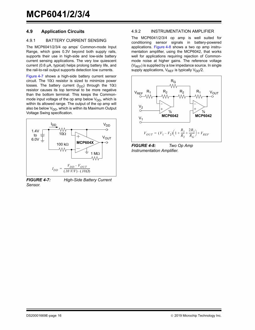
4.9 Application Circuits
4.9.1 BATTERY CURRENT SENSING
The MCP6041/2/3/4 op amps’ Common-mode InputRange, which goes 0.3V beyond both supply rails,supports their use in high-side and low-side batterycurrent sensing applications. The very low quiescentcurrent (0.6 µA, typical) helps prolong battery life, andthe rail-to-rail output supports detection low currents.
Figure 4-7 shows a high-side battery current sensorcircuit. The 10 resistor is sized to minimize powerlosses. The battery current (IDD) through the 10resistor causes its top terminal to be more negativethan the bottom terminal. This keeps the Common-mode input voltage of the op amp below VDD, which iswithin its allowed range. The output of the op amp willalso be below VDD, which is within its Maximum OutputVoltage Swing specification. .
FIGURE 4-7: High-Side Battery Current Sensor.
4.9.2 INSTRUMENTATION AMPLIFIER
The MCP6041/2/3/4 op amp is well suited forconditioning sensor signals in battery-poweredapplications. Figure 4-8 shows a two op amp instru-mentation amplifier, using the MCP6042, that workswell for applications requiring rejection of Common-mode noise at higher gains. The reference voltage(VREF) is supplied by a low impedance source. In singlesupply applications, VREF is typically VDD/2.
.
FIGURE 4-8: Two Op Amp Instrumentation Amplifier.
VDDIDD
MCP604X100 k
1 M
1.4V
VOUT
10to6.0V
IDD
VDD VOUT–10 V/V 10 ------------------------------------------=
VOUT V1 V2– 1R1R2------
2R1RG---------+ +
VREF+=
VREFR1 R2 R2 R1 VOUT
RG
V2
V1
½MCP6042
½MCP6042
DS20001669E-page 16 2019 Microchip Technology Inc.

MCP6041/2/3/4
5.0 DESIGN AIDS
Microchip provides the basic design tools needed forthe MCP6041/2/3/4 family of op amps.
5.1 SPICE Macro Model
The latest SPICE macro model for the MCP6041/2/3/4op amps is available on the Microchip web site atwww.microchip.com. This model is intended to be aninitial design tool that works well in the op amp’s linearregion of operation over the temperature range. Seethe model file for information on its capabilities.
Bench testing is a very important part of any design andcannot be replaced with simulations. Also, simulationresults using this macro model need to be validated bycomparing them to the data sheet specifications andcharacteristic curves.
5.2 FilterLab® Software
Microchip’s FilterLab® software is an innovativesoftware tool that simplifies analog active filter (usingop amps) design. Available at no cost from theMicrochip web site at www.microchip.com/filterlab, theFilterLab design tool provides full schematic diagramsof the filter circuit with component values. It alsooutputs the filter circuit in SPICE format, which can beused with the macro model to simulate actual filterperformance.
5.3 MAPS (Microchip Advanced Part Selector)
MAPS is a software tool that helps semiconductorprofessionals efficiently identify Microchip devices thatfit a particular design requirement. Available at no costfrom the Microchip website at www.microchip.com/maps, the MAPS is an overall selection tool forMicrochip’s product portfolio that includes Analog,Memory, MCUs and DSCs. Using this tool you candefine a filter to sort features for a parametric search ofdevices and export side-by-side technical comparisonreports. Helpful links are also provided for data sheets,purchase, and sampling of Microchip parts.
5.4 Analog Demonstration and Evaluation Boards
Microchip offers a broad spectrum of AnalogDemonstration and Evaluation Boards that aredesigned to help you achieve faster time to market. Fora complete listing of these boards and theircorresponding user’s guides and technical information,visit the Microchip web site at www.microchip.com/analogtools.
Some boards that are especially useful are:
• P/N SOIC8EV: 8-Pin SOIC/MSOP/TSSOP/DIP Evaluation Board
• P/N SOIC14EV: 14-Pin SOIC/TSSOP/DIP Evalu-ation Board
• MCP6XXX Amplifier Evaluation Board 1
• MCP6XXX Amplifier Evaluation Board 2
• MCP6XXX Amplifier Evaluation Board 3
• MCP6XXX Amplifier Evaluation Board 4
• Active Filter Demo Board Kit
5.5 Application Notes
The following Microchip Application Notes are avail-able on the Microchip web site at www.microchip.com/appnotes and are recommended as supplemental ref-erence resources:
ADN003: “Select the Right Operational Amplifier foryour Filtering Circuits,” DS21821
AN722: “Operational Amplifier Topologies and DCSpecifications,” DS00722
AN723: “Operational Amplifier AC Specifications andApplications,” DS00723
AN884: “Driving Capacitive Loads With Op Amps,”DS00884
AN990: “Analog Sensor Conditioning Circuits – AnOverview,” DS00990
These application notes and others are listed in thedesign guide:
“Signal Chain Design Guide,” DS21825
2019 Microchip Technology Inc. DS20001669E-page 17

MCP6041/2/3/4
NOTES:
DS20001669E-page 18 2019 Microchip Technology Inc.

MCP6041/2/3/4
6.0 PACKAGING INFORMATION
6.1 Package Marking Information
8-Lead MSOP Example:
5-Lead SOT-23 (MCP6041) Example:
XXNN 7X25Device
I-TempCode
E-TempCode
MCP6041/T-E/OT SPNN 7XNN
Note: Parts with date codes prior toNovember 2012 have their packagemarkings in the SBNN format.
6-Lead SOT-23 (MCP6043) Example:
XXNN SC25
Legend: XX...X Customer-specific informationY Year code (last digit of calendar year)YY Year code (last 2 digits of calendar year)WW Week code (week of January 1 is week ‘01’)NNN Alphanumeric traceability code Pb-free JEDEC designator for Matte Tin (Sn)* This package is Pb-free. The Pb-free JEDEC designator ( )
can be found on the outer packaging for this package.
Note: In the event the full Microchip part number cannot be marked on one line, it willbe carried over to the next line, thus limiting the number of availablecharacters for customer-specific information.
3e
3e
DeviceI-TempCode
E-TempCode
MCP6043T-E/CH SCNN SDNN
XXXXXXXXXXXXXNNN
YYWW
8-Lead PDIP (300 mil) Example:
MCP6041I/P256
1931
MCP6041I/P 256
19313eOR
6043I
931256
2019 Microchip Technology Inc. DS20001669E-page 19

MCP6041/2/3/4
Package Marking Information (Continued)
14-Lead PDIP (300 mil) (MCP6044) Example:
XXXXXXXXXXXXXXXXXXXXXXXXXXXX
YYWWNNN
MCP6044-I/P
1931256
MCP6044
1931256E/P 3eOR
14-Lead SOIC (150 mil) (MCP6044) Example:
XXXXXXXXXX
YYWWNNNXXXXXXXXXX
MCP6044ISL
1931256
MCP6044
1931256E/SL^^OR 3e
I/SL^3e
8-Lead SOIC (150 mil) Example:
XXXXXXXXXXXXYYWW
NNN
MCP6042I/SN1931
256
MCP6042ISN 1931
256OR 3e
DS20001669E-page 20 2019 Microchip Technology Inc.

MCP6041/2/3/4
Package Marking Information (Continued)
14-Lead TSSOP (MCP6044) Example:
XXXXXXXXYYWW
NNN
6044ST1931
256
6044EST1931
256OR
2019 Microchip Technology Inc. DS20001669E-page 21

MCP6041/2/3/4
0.15 C D2X
NOTE 1 1 2
N
TOP VIEW
SIDE VIEW
Microchip Technology Drawing C04-091-OT Rev E Sheet 1 of 2
For the most current package drawings, please see the Microchip Packaging Specification located athttp://www.microchip.com/packaging
Note:
0.20 C
C
SEATING PLANE
A A2
A1
e
NX bB0.20 C A-B D
e1
D
E1
E1/2
E/2
E
DA
0.20 C 2X
(DATUM D)(DATUM A-B)
A
ASEE SHEET 2
5-Lead Plastic Small Outline Transistor (OT) [SOT23]
DS20001669E-page 22 2019 Microchip Technology Inc.

MCP6041/2/3/4
Microchip Technology Drawing C04-091-OT Rev E Sheet 2 of 2
For the most current package drawings, please see the Microchip Packaging Specification located athttp://www.microchip.com/packaging
Note:
c
L
L1
VIEW A-ASHEET 1
5-Lead Plastic Small Outline Transistor (OT) [SOT23]
protrusions shall not exceed 0.25mm per side.1.
BSC: Basic Dimension. Theoretically exact value shown without tolerances.2.
Foot Angle
Number of PinsPitchOutside lead pitchOverall HeightMolded Package ThicknessStandoffOverall WidthMolded Package WidthOverall LengthFoot LengthFootprint
Lead ThicknessLead Width
Notes:
L1
bc
Dimension Limits
EE1DL
e1AA2A1
Units
Ne
0°0.080.20 -
--
10°0.260.51
MILLIMETERS
0.95 BSC1.90 BSC
0.30
0.900.89
-
0.60 REF
2.90 BSC-
2.80 BSC1.60 BSC
--
-
MIN5
NOM
1.451.300.15
0.60
MAX
REF: Reference Dimension, usually without tolerance, for information purposes only.
Dimensions D and E1 do not include mold flash or protrusions. Mold flash or
Dimensioning and tolerancing per ASME Y14.5M
2019 Microchip Technology Inc. DS20001669E-page 23

MCP6041/2/3/4
RECOMMENDED LAND PATTERN
5-Lead Plastic Small Outline Transistor (OT) [SOT23]
For the most current package drawings, please see the Microchip Packaging Specification located athttp://www.microchip.com/packaging
Note:
BSC: Basic Dimension. Theoretically exact value shown without tolerances.
Notes:1. Dimensioning and tolerancing per ASME Y14.5M
Microchip Technology Drawing No. C04-2091B [OT]
Dimension Limits
Contact Pad Length (X5)
Overall Width
Distance Between Pads
Contact Pad Width (X5)
Contact PitchContact Pad Spacing
3.90
1.10G
Z
Y1.70
0.60
MAXMIN
CX
E
UnitsNOM
0.95 BSC2.80
MILLIMETERS
Distance Between Pads GX 0.35
1
5
X
Y
Z C
E
GX
G
2
SILK SCREEN
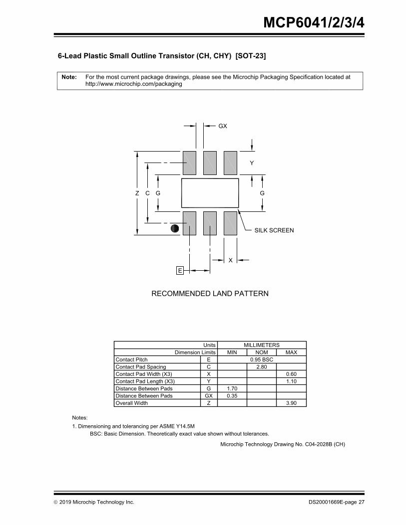
DS20001669E-page 24 2019 Microchip Technology Inc.

MCP6041/2/3/4
B
A
0.15 C A-B
0.15 C D
0.20 C A-B D
2X
TOP VIEW
SIDE VIEW
END VIEW
0.10 C
Microchip Technology Drawing C04-028C (CH) Sheet 1 of 2
2X
6X
For the most current package drawings, please see the Microchip Packaging Specification located athttp://www.microchip.com/packaging
Note:
6-Lead Plastic Small Outline Transistor (CH, CHY) [SOT-23]
D
EE1
e
e1
6X b
E2
E12
D
A A2
A1
L2
L(L1)
RR1
c
0.20 C A-B2X
C
SEATING PLANE
GAUGE PLANE
2019 Microchip Technology Inc. DS20001669E-page 25

MCP6041/2/3/4
Microchip Technology Drawing C04-028C (CH) Sheet 2 of 2
6-Lead Plastic Small Outline Transistor (CH, CHY) [SOT-23]
For the most current package drawings, please see the Microchip Packaging Specification located athttp://www.microchip.com/packaging
Note:
protrusions shall not exceed 0.25mm per side.1.
BSC: Basic Dimension. Theoretically exact value shown without tolerances.2.
Notes:
REF: Reference Dimension, usually without tolerance, for information purposes only.
Dimensions D and E1 do not include mold flash or protrusions. Mold flash or
Dimensioning and tolerancing per ASME Y14.5M
Foot Angle
Number of LeadsPitchOutside lead pitchOverall HeightMolded Package ThicknessStandoffOverall WidthMolded Package WidthOverall LengthFoot LengthFootprint
Lead ThicknessLead Width
L1
φ
bc
Dimension Limits
EE1DL
e1AA2A1
Units
Ne
0°0.080.20 -
--
10°0.260.51
MILLIMETERS
0.95 BSC1.90 BSC
0.30
0.900.890.00
0.60 REF
2.90 BSC0.45
2.80 BSC1.60 BSC
1.15-
-
MIN6
NOM
1.451.300.15
0.60
MAX
Seating Plane to Gauge Plane L1 0.25 BSC
DS20001669E-page 26 2019 Microchip Technology Inc.
MCP6041/2/3/4
RECOMMENDED LAND PATTERN
Microchip Technology Drawing No. C04-2028B (CH)
6-Lead Plastic Small Outline Transistor (CH, CHY) [SOT-23]
For the most current package drawings, please see the Microchip Packaging Specification located athttp://www.microchip.com/packaging
Note:
BSC: Basic Dimension. Theoretically exact value shown without tolerances.
Notes:1. Dimensioning and tolerancing per ASME Y14.5M
Dimension Limits
Contact Pad Length (X3)
Overall Width
Distance Between Pads
Contact Pad Width (X3)
Contact PitchContact Pad Spacing
3.90
1.10G
Z
Y1.70
0.60
MAXMIN
CX
E
UnitsNOM
0.95 BSC2.80
MILLIMETERS
Distance Between Pads GX 0.35
E
X
GX
Y
GCZ
SILK SCREEN
G
2019 Microchip Technology Inc. DS20001669E-page 27

MCP6041/2/3/4
Note: For the most current package drawings, please see the Microchip Packaging Specification located at http://www.microchip.com/packaging
DS20001669E-page 28 2019 Microchip Technology Inc.

MCP6041/2/3/4
Note: For the most current package drawings, please see the Microchip Packaging Specification located at http://www.microchip.com/packaging
2019 Microchip Technology Inc. DS20001669E-page 29

MCP6041/2/3/4
Note: For the most current package drawings, please see the Microchip Packaging Specification located at http://www.microchip.com/packaging
DS20001669E-page 30 2019 Microchip Technology Inc.

MCP6041/2/3/4
B
A
For the most current package drawings, please see the Microchip Packaging Specification located athttp://www.microchip.com/packaging
Note:
Microchip Technology Drawing No. C04-018-P Rev E Sheet 1 of 2
8-Lead Plastic Dual In-Line (P) - 300 mil Body [PDIP]
eB
E
A
A1
A2
L
8X b
8X b1
E1
c
C
PLANE
.010 C
1 2
N
D
NOTE 1
TOP VIEW
END VIEWSIDE VIEW
e
2019 Microchip Technology Inc. DS20001669E-page 31

MCP6041/2/3/4
Microchip Technology Drawing No. C04-018-P Rev E Sheet 2 of 2
For the most current package drawings, please see the Microchip Packaging Specification located athttp://www.microchip.com/packaging
Note:
8-Lead Plastic Dual In-Line (P) - 300 mil Body [PDIP]
Units INCHESDimension Limits MIN NOM MAX
Number of Pins N 8Pitch e .100 BSCTop to Seating Plane A - - .210Molded Package Thickness A2 .115 .130 .195Base to Seating Plane A1 .015Shoulder to Shoulder Width E .290 .310 .325Molded Package Width E1 .240 .250 .280Overall Length D .348 .365 .400Tip to Seating Plane L .115 .130 .150Lead Thickness c .008 .010 .015Upper Lead Width b1 .040 .060 .070Lower Lead Width b .014 .018 .022Overall Row Spacing eB - - .430
BSC: Basic Dimension. Theoretically exact value shown without tolerances.
3.
1.
protrusions shall not exceed .010" per side.
2.
4.
Notes:
§
- -
Dimensions D and E1 do not include mold flash or protrusions. Mold flash or
Pin 1 visual index feature may vary, but must be located within the hatched area.§ Significant Characteristic
Dimensioning and tolerancing per ASME Y14.5M
e
DATUM A DATUM A
e
be2
be2
ALTERNATE LEAD DESIGN(NOTE 5)
5. Lead design above seating plane may vary, based on assembly vendor.
DS20001669E-page 32 2019 Microchip Technology Inc.

MCP6041/2/3/4
0.25 C A–B D
CSEATING
PLANE
TOP VIEW
SIDE VIEW
VIEW A–A
0.10 C
0.10 C
Microchip Technology Drawing No. C04-057-SN Rev E Sheet 1 of 2
8X
For the most current package drawings, please see the Microchip Packaging Specification located athttp://www.microchip.com/packaging
Note:
8-Lead Plastic Small Outline (SN) - Narrow, 3.90 mm (.150 In.) Body [SOIC]
1 2
N
h
h
A1
A2A
A
B
e
D
E
E2
E12
E1
NOTE 5
NOTE 5
NX b
0.10 C A–B2X
H 0.23
(L1)L
R0.13
R0.13
VIEW C
SEE VIEW C
NOTE 1
D
2019 Microchip Technology Inc. DS20001669E-page 33

MCP6041/2/3/4
Microchip Technology Drawing No. C04-057-SN Rev E Sheet 2 of 2
8-Lead Plastic Small Outline (SN) - Narrow, 3.90 mm (.150 In.) Body [SOIC]
For the most current package drawings, please see the Microchip Packaging Specification located athttp://www.microchip.com/packaging
Note:
Foot Angle 0° - 8°
15°-5°Mold Draft Angle Bottom15°-5°Mold Draft Angle Top0.51-0.31bLead Width0.25-0.17cLead Thickness
1.27-0.40LFoot Length0.50-0.25hChamfer (Optional)
4.90 BSCDOverall Length3.90 BSCE1Molded Package Width6.00 BSCEOverall Width
0.25-0.10A1Standoff--1.25A2Molded Package Thickness
1.75--AOverall Height1.27 BSCePitch
8NNumber of PinsMAXNOMMINDimension Limits
MILLIMETERSUnits
protrusions shall not exceed 0.15mm per side.3. Dimensions D and E1 do not include mold flash or protrusions. Mold flash or
REF: Reference Dimension, usually without tolerance, for information purposes only.BSC: Basic Dimension. Theoretically exact value shown without tolerances.
1. Pin 1 visual index feature may vary, but must be located within the hatched area.2. § Significant Characteristic
4. Dimensioning and tolerancing per ASME Y14.5M
Notes:
§
Footprint L1 1.04 REF
5. Datums A & B to be determined at Datum H.
DS20001669E-page 34 2019 Microchip Technology Inc.

MCP6041/2/3/4
RECOMMENDED LAND PATTERN
Microchip Technology Drawing C04-2057-SN Rev E
8-Lead Plastic Small Outline (SN) - Narrow, 3.90 mm Body [SOIC]
BSC: Basic Dimension. Theoretically exact value shown without tolerances.
Notes:Dimensioning and tolerancing per ASME Y14.5M1.
For the most current package drawings, please see the Microchip Packaging Specification located athttp://www.microchip.com/packaging
Note:
Dimension LimitsUnits
CContact Pad SpacingContact Pitch
MILLIMETERS
1.27 BSCMIN
EMAX
5.40
Contact Pad Length (X8)Contact Pad Width (X8)
Y1X1
1.550.60
NOM
E
X1
C
Y1
SILK SCREEN
2019 Microchip Technology Inc. DS20001669E-page 35

MCP6041/2/3/4
! "" # $% $ &&'$ * " $+%#3*7%
9;9"<
=$> $%$>$ $;??$?$>
@ GJK#"Q %GJ JU% %+Y
J J * &&9<$ + Z Z &% ><> + 7 !& [79 + &7 Z Z \ # [& !& !7% >\ # *& 7& ]&UQ " ^!7 ^7& ^^7<$ Q 7 !& 7&Q <> &&] && &7@$$Q \ &*7 &_& &^&QQ \ &* &] &U`$ 9 Z Z *!&
N
E1
D
NOTE 1
1 2 3
E
c
eB
A2
L
A
A1b1
b e
%$ < " &*j&&79
DS20001669E-page 36 2019 Microchip Technology Inc.

MCP6041/2/3/4
Microchip Technology Drawing No. C04-065-SL Rev D Sheet 1 of 2
For the most current package drawings, please see the Microchip Packaging Specification located athttp://www.microchip.com/packaging
Note:
14-Lead Plastic Small Outline (SL) - Narrow, 3.90 mm Body [SOIC]
0.20 C
0.25 C A–B D
1 2
N
2X N/2 TIPS
TOP VIEW
SIDE VIEW
VIEW A–A
A
e
B
E
D
E2
D
E1
E22
NX b
A1
A2ACSEATING
PLANE
0.10 C14X
0.10 C A–B
0.10 C D
c
hh
H
SEE VIEW C
(L1)L
R0.13R0.13
VIEW C
NOTE 1 3
0.10 C
NOTE 5
NOTE 5
2X
2X
2019 Microchip Technology Inc. DS20001669E-page 37

MCP6041/2/3/4
Microchip Technology Drawing No. C04-065-SL Rev D Sheet 2 of 2
14-Lead Plastic Small Outline (SL) - Narrow, 3.90 mm Body [SOIC]
For the most current package drawings, please see the Microchip Packaging Specification located athttp://www.microchip.com/packaging
Note:
Foot Angle 0° - 8°
15°-5°Mold Draft Angle Bottom15°-5°Mold Draft Angle Top0.51-0.31bLead Width0.25-0.10cLead Thickness
1.04 REFL1Footprint
0.50-0.25hChamfer (Optional)8.65 BSCDOverall Length3.90 BSCE1Molded Package Width6.00 BSCEOverall Width
0.25-0.10A1Standoff--1.25A2Molded Package Thickness
1.75--AOverall Height1.27 BSCePitch
14NNumber of PinsMAXNOMMINDimension Limits
MILLIMETERSUnits
Foot Length L 0.40 - 1.27
§
or protrusion, which shall not exceed 0.25 mm per side.
3.
REF: Reference Dimension, usually without tolerance, for information purposes only.BSC: Basic Dimension. Theoretically exact value shown without tolerances.
1.2.
4.
Notes:
Dimension D does not include mold flash, protrusions or gate burrs, which shall
Pin 1 visual index feature may vary, but must be located within the hatched area.§ Significant Characteristic
Dimensioning and tolerancing per ASME Y14.5M
not exceed 0.15 mm per end. Dimension E1 does not include interlead flash
5. Datums A & B to be determined at Datum H.
Lead Angle 0° - -
DS20001669E-page 38 2019 Microchip Technology Inc.

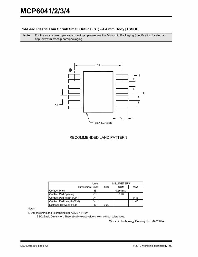
MCP6041/2/3/4
RECOMMENDED LAND PATTERN
Dimension LimitsUnits
Contact Pitch
MILLIMETERS
1.27 BSCMIN
EMAX
Contact Pad Length (X14)Contact Pad Width (X14)
YX
1.550.60
NOM
CContact Pad Spacing 5.40
BSC: Basic Dimension. Theoretically exact value shown without tolerances.
Notes:Dimensioning and tolerancing per ASME Y14.5M1.
For the most current package drawings, please see the Microchip Packaging Specification located athttp://www.microchip.com/packaging
Note:
E
X
Y
C
SILK SCREEN
Microchip Technology Drawing No. C04-2065-SL Rev D
14-Lead Plastic Small Outline (SL) - Narrow, 3.90 mm Body [SOIC]
1 2
14
2019 Microchip Technology Inc. DS20001669E-page 39

MCP6041/2/3/4
Note: For the most current package drawings, please see the Microchip Packaging Specification located at http://www.microchip.com/packaging
DS20001669E-page 40 2019 Microchip Technology Inc.

MCP6041/2/3/4
Note: For the most current package drawings, please see the Microchip Packaging Specification located at http://www.microchip.com/packaging
2019 Microchip Technology Inc. DS20001669E-page 41
MCP6041/2/3/4
Note: For the most current package drawings, please see the Microchip Packaging Specification located at http://www.microchip.com/packaging
DS20001669E-page 42 2019 Microchip Technology Inc.

MCP6041/2/3/4
APPENDIX A: REVISION HISTORY
Revision E (November 2019)
The following is the list of modifications:
1. Updated Section 6.0 “Packaging Informa-tion”.
Revision D (March 2013)
The following is the list of modifications:
1. Updated the boards list in Section 5.4 “AnalogDemonstration and Evaluation Boards”.
2. Removed the Mindi™ Circuit Designer &Simulator section.
3. Updated the E-Temp Code value for the 5-LeadSOT-23 package in Section 6.0 “PackagingInformation”.
Revision C (February 2008)
The following is the list of modifications:
1. Updated Figure 2-4 and Figure 2-5.
2. Updated trademark and Sales listing pages.
3. Expanded this op amp family:
4. Added the SOT-23-6 package for the MCP6043op amp with Chip Select.
5. Added Extended Temperature (-40°C to+125°C) parts.
6. Expanded Analog Input Absolute Max VoltageRange (applies retroactively).
7. Expanded operating VDD to a maximum of 6.0V.
8. Section 1.0 “Electrical Characteristics”updated.
9. Section 2.0 “Typical Performance Curves”updated.
10. Section 3.0 “Pin Descriptions” added.
11. Section 4.0 “Applications Information” added.
12. Added Section 4.7 “Unused Op Amps”.
13. Updated input stage explanation.
14. Section 5.0 “Design Aids” updated.
15. Section 6.0 “Packaging Information” updated.
16. Added SOT-23-6 package.
17. Corrected package marking information.
18. Appendix A: “Revision History” added.
Revision B (June 2002)
The following is the list of modifications.
• Undocumented changes.
Revision A (August 2001)
• Original data sheet release.
2019 Microchip Technology Inc. DS20001669E-page 39

MCP6041/2/3/4
NOTES:
DS20001669E-page 40 2019 Microchip Technology Inc.

MCP6041/2/3/4
PRODUCT IDENTIFICATION SYSTEM
To order or obtain information, e.g., on pricing or delivery, refer to the factory or the listed sales office.
PART NO. X /XX
PackageTemperatureRange
Device
Device: MCP6041: Single Op AmpMCP6041T Single Op Amp
(Tape and Reel for SOT-23, SOIC, MSOP)MCP6042 Dual Op AmpMCP6042T Dual Op Amp
(Tape and Reel for SOIC and MSOP)MCP6043 Single Op Amp w/ Chip SelectMCP6043T Single Op Amp w/ Chip Select
(Tape and Reel for SOT-23, SOIC, MSOP)MCP6044 Quad Op AmpMCP6044T Quad Op Amp
(Tape and Reel for SOIC and TSSOP)
Temperature Range: I = -40°C to +85°CE = -40°C to +125°C
Package: CH = Plastic Small Outline Transistor (SOT-23),6-lead (Tape and Reel - MCP6043 only)
MS = Plastic Micro Small Outline (MSOP), 8-leadOT = Plastic Small Outline Transistor (SOT-23),
5-lead (Tape and Reel - MCP6041 only)P = Plastic DIP (300 mil Body), 8-lead, 14-leadSL = Plastic SOIC (150 mil Body), 14-leadSN = Plastic SOIC (150 mil Body), 8-leadST = Plastic TSSOP (4.4 mm Body), 14-lead
Examples:
a) MCP6041-I/P: Industrial Temperature,8LD PDIP package.
b) MCP6041T-E/OT: Tape and Reel,Extended Temperature,5LD SOT-23 package.
a) MCP6042-I/SN: Industrial Temperature,8LD SOIC package.
b) MCP6042T-E/MS: Tape and Reel,Extended Temperature,8LD MSOP package.
a) MCP6043-I/P: Industrial Temperature,8LD PDIP package.
b) MCP6043T-E/CH: Tape and Reel,Extended Temperature,6LD SOT-23 package.
a) MCP6044-I/SL: Industrial Temperature,14LD SOIC package.
b) MCP6044T-E/ST: Tape and Reel,Extended Temperature,14LD TSSOP package.
2019 Microchip Technology Inc. DS20001669E-page 41
MCP6041/2/3/4
NOTES:
DS20001669E-page 42 2019 Microchip Technology Inc.
Note the following details of the code protection feature on Microchip devices:
• Microchip products meet the specification contained in their particular Microchip Data Sheet.
• Microchip believes that its family of products is one of the most secure families of its kind on the market today, when used in the intended manner and under normal conditions.
• There are dishonest and possibly illegal methods used to breach the code protection feature. All of these methods, to our knowledge, require using the Microchip products in a manner outside the operating specifications contained in Microchip’s Data Sheets. Most likely, the person doing so is engaged in theft of intellectual property.
• Microchip is willing to work with the customer who is concerned about the integrity of their code.
• Neither Microchip nor any other semiconductor manufacturer can guarantee the security of their code. Code protection does not mean that we are guaranteeing the product as “unbreakable.”
Code protection is constantly evolving. We at Microchip are committed to continuously improving the code protection features of ourproducts. Attempts to break Microchip’s code protection feature may be a violation of the Digital Millennium Copyright Act. If such actsallow unauthorized access to your software or other copyrighted work, you may have a right to sue for relief under that Act.
Information contained in this publication regarding deviceapplications and the like is provided only for your convenienceand may be superseded by updates. It is your responsibility toensure that your application meets with your specifications.MICROCHIP MAKES NO REPRESENTATIONS ORWARRANTIES OF ANY KIND WHETHER EXPRESS ORIMPLIED, WRITTEN OR ORAL, STATUTORY OROTHERWISE, RELATED TO THE INFORMATION,INCLUDING BUT NOT LIMITED TO ITS CONDITION,QUALITY, PERFORMANCE, MERCHANTABILITY ORFITNESS FOR PURPOSE. Microchip disclaims all liabilityarising from this information and its use. Use of Microchipdevices in life support and/or safety applications is entirely atthe buyer’s risk, and the buyer agrees to defend, indemnify andhold harmless Microchip from any and all damages, claims,suits, or expenses resulting from such use. No licenses areconveyed, implicitly or otherwise, under any Microchipintellectual property rights unless otherwise stated.
2019 Microchip Technology Inc.
For information regarding Microchip’s Quality Management Systems, please visit www.microchip.com/quality.
TrademarksThe Microchip name and logo, the Microchip logo, Adaptec, AnyRate, AVR, AVR logo, AVR Freaks, BesTime, BitCloud, chipKIT, chipKIT logo, CryptoMemory, CryptoRF, dsPIC, FlashFlex, flexPWR, HELDO, IGLOO, JukeBlox, KeeLoq, Kleer, LANCheck, LinkMD, maXStylus, maXTouch, MediaLB, megaAVR, Microsemi, Microsemi logo, MOST, MOST logo, MPLAB, OptoLyzer, PackeTime, PIC, picoPower, PICSTART, PIC32 logo, PolarFire, Prochip Designer, QTouch, SAM-BA, SenGenuity, SpyNIC, SST, SST Logo, SuperFlash, Symmetricom, SyncServer, Tachyon, TempTrackr, TimeSource, tinyAVR, UNI/O, Vectron, and XMEGA are registered trademarks of Microchip Technology Incorporated in the U.S.A. and other countries.
APT, ClockWorks, The Embedded Control Solutions Company, EtherSynch, FlashTec, Hyper Speed Control, HyperLight Load, IntelliMOS, Libero, motorBench, mTouch, Powermite 3, Precision Edge, ProASIC, ProASIC Plus, ProASIC Plus logo, Quiet-Wire, SmartFusion, SyncWorld, Temux, TimeCesium, TimeHub, TimePictra, TimeProvider, Vite, WinPath, and ZL are registered trademarks of Microchip Technology Incorporated in the U.S.A.
Adjacent Key Suppression, AKS, Analog-for-the-Digital Age, Any Capacitor, AnyIn, AnyOut, BlueSky, BodyCom, CodeGuard, CryptoAuthentication, CryptoAutomotive, CryptoCompanion, CryptoController, dsPICDEM, dsPICDEM.net, Dynamic Average Matching, DAM, ECAN, EtherGREEN, In-Circuit Serial Programming, ICSP, INICnet, Inter-Chip Connectivity, JitterBlocker, KleerNet, KleerNet logo, memBrain, Mindi, MiWi, MPASM, MPF, MPLAB Certified logo, MPLIB, MPLINK, MultiTRAK, NetDetach, Omniscient Code Generation, PICDEM, PICDEM.net, PICkit, PICtail, PowerSmart, PureSilicon, QMatrix, REAL ICE, Ripple Blocker, SAM-ICE, Serial Quad I/O, SMART-I.S., SQI, SuperSwitcher, SuperSwitcher II, Total Endurance, TSHARC, USBCheck, VariSense, ViewSpan, WiperLock, Wireless DNA, and ZENA are trademarks of Microchip Technology Incorporated in the U.S.A. and other countries.
SQTP is a service mark of Microchip Technology Incorporated in the U.S.A.The Adaptec logo, Frequency on Demand, Silicon Storage Technology, and Symmcom are registered trademarks of Microchip Technology Inc. in other countries.GestIC is a registered trademark of Microchip Technology Germany II GmbH & Co. KG, a subsidiary of Microchip Technology Inc., in other countries. All other trademarks mentioned herein are property of their respective companies.
© 2019, Microchip Technology Incorporated, All Rights Reserved.
ISBN: 978-1-5224-5306-2
DS20001669E-page 43

DS20001669E-page 44 2019 Microchip Technology Inc.
AMERICASCorporate Office2355 West Chandler Blvd.Chandler, AZ 85224-6199Tel: 480-792-7200 Fax: 480-792-7277Technical Support: http://www.microchip.com/supportWeb Address: www.microchip.com
AtlantaDuluth, GA Tel: 678-957-9614 Fax: 678-957-1455
Austin, TXTel: 512-257-3370
BostonWestborough, MA Tel: 774-760-0087 Fax: 774-760-0088
ChicagoItasca, IL Tel: 630-285-0071 Fax: 630-285-0075
DallasAddison, TX Tel: 972-818-7423 Fax: 972-818-2924
DetroitNovi, MI Tel: 248-848-4000
Houston, TX Tel: 281-894-5983
IndianapolisNoblesville, IN Tel: 317-773-8323Fax: 317-773-5453Tel: 317-536-2380
Los AngelesMission Viejo, CA Tel: 949-462-9523Fax: 949-462-9608Tel: 951-273-7800
Raleigh, NC Tel: 919-844-7510
New York, NY Tel: 631-435-6000
San Jose, CA Tel: 408-735-9110Tel: 408-436-4270
Canada - TorontoTel: 905-695-1980 Fax: 905-695-2078
ASIA/PACIFICAustralia - SydneyTel: 61-2-9868-6733
China - BeijingTel: 86-10-8569-7000
China - ChengduTel: 86-28-8665-5511
China - ChongqingTel: 86-23-8980-9588
China - DongguanTel: 86-769-8702-9880
China - GuangzhouTel: 86-20-8755-8029
China - HangzhouTel: 86-571-8792-8115
China - Hong Kong SARTel: 852-2943-5100
China - NanjingTel: 86-25-8473-2460
China - QingdaoTel: 86-532-8502-7355
China - ShanghaiTel: 86-21-3326-8000
China - ShenyangTel: 86-24-2334-2829
China - ShenzhenTel: 86-755-8864-2200
China - SuzhouTel: 86-186-6233-1526
China - WuhanTel: 86-27-5980-5300
China - XianTel: 86-29-8833-7252
China - XiamenTel: 86-592-2388138
China - ZhuhaiTel: 86-756-3210040
ASIA/PACIFICIndia - BangaloreTel: 91-80-3090-4444
India - New DelhiTel: 91-11-4160-8631
India - PuneTel: 91-20-4121-0141
Japan - OsakaTel: 81-6-6152-7160
Japan - TokyoTel: 81-3-6880- 3770
Korea - DaeguTel: 82-53-744-4301
Korea - SeoulTel: 82-2-554-7200
Malaysia - Kuala LumpurTel: 60-3-7651-7906
Malaysia - PenangTel: 60-4-227-8870
Philippines - ManilaTel: 63-2-634-9065
SingaporeTel: 65-6334-8870
Taiwan - Hsin ChuTel: 886-3-577-8366
Taiwan - KaohsiungTel: 886-7-213-7830
Taiwan - TaipeiTel: 886-2-2508-8600
Thailand - BangkokTel: 66-2-694-1351
Vietnam - Ho Chi MinhTel: 84-28-5448-2100
EUROPEAustria - WelsTel: 43-7242-2244-39Fax: 43-7242-2244-393
Denmark - CopenhagenTel: 45-4450-2828 Fax: 45-4485-2829
Finland - EspooTel: 358-9-4520-820
France - ParisTel: 33-1-69-53-63-20 Fax: 33-1-69-30-90-79
Germany - GarchingTel: 49-8931-9700
Germany - HaanTel: 49-2129-3766400
Germany - HeilbronnTel: 49-7131-72400
Germany - KarlsruheTel: 49-721-625370
Germany - MunichTel: 49-89-627-144-0 Fax: 49-89-627-144-44
Germany - RosenheimTel: 49-8031-354-560
Israel - Ra’anana Tel: 972-9-744-7705
Italy - Milan Tel: 39-0331-742611 Fax: 39-0331-466781
Italy - PadovaTel: 39-049-7625286
Netherlands - DrunenTel: 31-416-690399 Fax: 31-416-690340
Norway - TrondheimTel: 47-7288-4388
Poland - WarsawTel: 48-22-3325737
Romania - BucharestTel: 40-21-407-87-50
Spain - MadridTel: 34-91-708-08-90Fax: 34-91-708-08-91
Sweden - GothenbergTel: 46-31-704-60-40
Sweden - StockholmTel: 46-8-5090-4654
UK - WokinghamTel: 44-118-921-5800Fax: 44-118-921-5820
Worldwide Sales and Service
05/14/19


![Dan Alistarh, Rati Gelashvili, Milan Vojnovic´ February ... · Dan Alistarh, Rati Gelashvili, Milan Vojnovic´ ... [DMST07]; also, this task is a key component when simulating register](https://static.fdocuments.in/doc/165x107/5cceb93588c993fb7c8d7282/dan-alistarh-rati-gelashvili-milan-vojnovic-february-dan-alistarh-rati.jpg)