MCP2210 USB-to-SPI Protocol Converter with GPIO...
82
2011 Microchip Technology Inc. DS22288A-page 1 MCP2210 Features: Universal Serial Bus (USB) • Supports Full-Speed USB (12 Mb/s) • Human Interface Device (HID) device • 128-Byte Buffer to Handle Data Throughput: - 64-byte transmit - 64-byte receive • Fully Configurable VID, PID Assignments and String Descriptor (factory programming also avail- able) • Bus Powered (factory default) or Self-Powered (can be selected through special USB commands) • USB 2.0 Compliant USB Driver and Software Support • Uses Standard HID Drivers (built-in support on Windows ® XP, Vista, 7, Linux and Mac OS ® ) • Configuration Utility for Device’s Power-up Configuration • Utility for USB-SPI Communication, GPIO Manipulation and Miscellaneous Features Usage SPI Master Peripheral • Supports all Four SPI modes (Mode 0, 1, 2, 3) • Bit Rates from 1500 bps up to 12 Mbps • Configurable Delays for SPI Transactions: - Chip Select (assert) to 1 st byte of data delay - Data to data delay - Data to Chip Select (de-assert) delay • SPI Transactions Lengths of up to 65535 Bytes Long • Up to 9 Chip Select lines – to be used in any combination for a given SPI transaction (the Chip Select lines are shared between GPIOs and alternate function pins; certain GPs – up to 9 of them – can be assigned with the Chip Select functionality) General Purpose Input/Output (GPIO) Pins • Nine General Purpose I/O Pins EEPROM • 256 Bytes of User EEPROM (accessible through certain USB commands) Package Types: The device will be offered in the following packages: • 20-lead QFN (5 x 5 mm) • 20-lead SOIC • 20-lead SSOP Other • USB Activity LED Output • SSPND Output Pin (to signal USB Suspend state) • USBCFG Output Pin (indicates when the enumeration is completed) • Operating Voltage: 3.3-5.5V • Oscillator Input: 12 MHz • Industrial Operating Temperature: -40°C to +85°C 2 MCP2210 SOIC, SSOP OSC2 OSC1 RST 1 2 3 4 20 19 18 17 VDD VSS D+ D- VUSB GP0 5 16 GP8 GP1 6 15 GP2 7 14 GP6 GP7 MCP2210 5x5 QFN* GP1 GP2 RST D- VUSB MOSI GP8 GP4 SCK GP5 GP7 OSC2 OSC1 VDD VSS GP0 EP 20 1 19 18 17 3 4 15 14 13 12 6 7 8 9 21 13 12 1 1 MISO GP5 SCK GP3 8 MOSI 9 GP4 10 D+ 16 GP3 GP6 5 11 MISO 10 * Includes Exposed Thermal Pad (EP); see Table 1-1. USB-to-SPI Protocol Converter with GPIO (Master Mode)
Transcript of MCP2210 USB-to-SPI Protocol Converter with GPIO...

MCP2210USB-to-SPI Protocol Converter with GPIO (Master Mode)
Features:
Universal Serial Bus (USB)• Supports Full-Speed USB (12 Mb/s)• Human Interface Device (HID) device• 128-Byte Buffer to Handle Data Throughput:
- 64-byte transmit- 64-byte receive
• Fully Configurable VID, PID Assignments and String Descriptor (factory programming also avail-able)
• Bus Powered (factory default) or Self-Powered (can be selected through special USB commands)
• USB 2.0 Compliant
USB Driver and Software Support• Uses Standard HID Drivers (built-in support on
Windows® XP, Vista, 7, Linux and Mac OS®)• Configuration Utility for Device’s Power-up
Configuration• Utility for USB-SPI Communication, GPIO
Manipulation and Miscellaneous Features Usage
SPI Master Peripheral• Supports all Four SPI modes (Mode 0, 1, 2, 3)• Bit Rates from 1500 bps up to 12 Mbps• Configurable Delays for SPI Transactions:
- Chip Select (assert) to 1st byte of data delay- Data to data delay- Data to Chip Select (de-assert) delay
• SPI Transactions Lengths of up to 65535 Bytes Long
• Up to 9 Chip Select lines – to be used in any combination for a given SPI transaction (the Chip Select lines are shared between GPIOs and alternate function pins; certain GPs – up to 9 of them – can be assigned with the Chip Select functionality)
General Purpose Input/Output (GPIO) Pins• Nine General Purpose I/O Pins
EEPROM• 256 Bytes of User EEPROM (accessible through
certain USB commands)
Package Types:The device will be offered in the following packages:• 20-lead QFN (5 x 5 mm)• 20-lead SOIC• 20-lead SSOP
Other• USB Activity LED Output• SSPND Output Pin (to signal USB Suspend state)• USBCFG Output Pin (indicates when the
enumeration is completed)• Operating Voltage: 3.3-5.5V• Oscillator Input: 12 MHz• Industrial Operating Temperature: -40°C to +85°C
2
MCP2210SOIC, SSOP
OSC2OSC1
RST
1234
20191817
VDD VSS
D+
D-VUSB
GP0 5 16 GP8GP1 6 15GP2 7 14 GP6
GP7
MCP22105x5 QFN*
GP1GP2
RST D-
VUSB
MO
SI
GP8
GP
4
SC
K
GP
5
GP7
OS
C2
OS
C1
VD
D
VS
S
GP0EP
201
19 18 17
3
4
15
1413
12
6 7 8 9
21
131211
MISO
GP5
SCK
GP3 8MOSI 9
GP4 10
D+
16
GP3 GP65 11
MIS
O
10
* Includes Exposed Thermal Pad (EP); see Table 1-1.
2011 Microchip Technology Inc. DS22288A-page 1

MCP2210
Block DiagramGPIO
ControlUSB
Protocol Controller
USB XCVR
VSS OSC
State Clock
USB Clock
Reset
3.3V LDO
256-Byte EEPROM
Configuration and Control
Regs
SPI (Master)
Baud Generator
Chip Select
Control
GP8-GP0
D+
D-
VUSB
VDDRSTOSC1 OSC2Vss
MOSIMISO
SCK
CS8:0
Dedicated function pins
DS22288A-page 2 2011 Microchip Technology Inc.

MCP2210
1.0 FUNCTIONAL DESCRIPTIONThe MCP2210 device is a USB-to-SPI Masterconverter which enables USB connectivity inapplications that have an SPI interface. The devicereduces external components by integrating the USBtermination resistors.
The MCP2210 also has 256 bytes of integrated userEEPROM.
The MCP2210 has nine general purpose input/outputpins. Seven pins have alternate functions to indicateUSB and communication status. See Table 1-1 andSection 1.6 “GP Module” for details about the pinfunctions.
TABLE 1-1: PINOUT DESCRIPTIONMCP2210
Symbol Type
Stan
dard
Fun
ctio
n(G
PIO
)
Alte
rnat
e Fu
nctio
n 1
(Chi
p Se
lect
s)
Alte
rnat
e Fu
nctio
n 2
(ded
icat
ed fu
nctio
ns)
DescriptionQFN SOIC,
SSOP
1 4 RST I — — — Reset input
2 5 GP0 I/O GPIO0 CS0 — General Purpose I/O3 6 GP1 I/O GPIO1 CS1 — General Purpose I/O4 7 GP2 I/O GPIO2 CS2 USB Suspend General Purpose I/O5 8 GP3 I/O GPIO3 CS3 SPI Transfer Traffic LED General Purpose I/O6 9 MOSI O — — — SPI Master output7 10 GP4 I/O GPIO4 CS4 USB Low Power General Purpose I/O8 11 SCK O — — — SPI Clock output9 12 GP5 I/O GPIO5 CS5 USB Configured General Purpose I/O
10 13 MISO I — — — SPI Master input11 14 GP6 I/O GPIO6 CS6 External Interrupt General Purpose I/O12 15 GP7 I/O GPIO7 CS7 SPI Bus Release ACK General Purpose I/O13 16 GP8 I/O GPIO8 CS8 SPI Bus Release REQ General Purpose I/O14 17 VUSB USB — — — USB Regulator output15 18 D- USB — — — USB D-16 19 D+ USB — — — USB D+17 20 VSS GND — — — Ground18 1 VDD P — — — Power19 2 OSC1 I — — — Oscillator input20 3 OSC2 O — — — Oscillator output
2011 Microchip Technology Inc. DS22288A-page 3

MCP2210
1.1 Supported Operating SystemsThe following operating systems are supported:• Windows XP/Vista/7• Linux• Mac OS
1.1.1 ENUMERATIONThe MCP2210 will enumerate as a USB device afterPower-on Reset (POR). The device enumerates as aHuman Interface Device (HID) only.
1.1.1.1 Human Interface Device (HID)The MCP2210 enumerates as an HID, so the devicecan be configured and all the other functionalities canbe controlled. A DLL package that facilitates I/O controlthrough a custom interface is supplied by Microchipand is available on the product landing page.
1.2 Control ModuleThe control module is the heart of the MCP2210. Allother modules are tied together and controlled via thecontrol module. The control module manages the datatransfers between the USB and the SPI, as well ascommand requests generated by the USB hostcontroller, and commands for controlling the function ofthe SPI and I/O.
1.2.1 SPI INTERFACEThe control module interfaces to the SPI and USBmodules.
1.2.2 INTERFACING TO THE DEVICEThe MCP2210 can be accessed for reading and writingvia USB host commands. The device cannot beaccessed and controlled via the SPI interface.
1.3 SPI ModuleThe MCP2210 SPI module provides the MOSI, MISOand SCK signals to the outside world. The module hasthe ability to control the GP pins (as Chip Select) only ifthese pins are configured for Chip Select operation.
1.3.1 SPI MODULE FEATURESThe SPI module has the following configurablefeatures:
• Bit rates• Delays• Chip Select pin assignments (up to 9 Chip Select
lines)
All the above features are available for customizationusing certain USB commands.
1.3.2 SPI MODULE POWER-UP CONFIGURATION
Default parameters:
• 1 Mbit• 4 bytes to transfer per SPI transaction• GP1 as Chip Select line
1.4 USB Protocol ControllerThe USB controller in the MCP2210 is full-speed USB2.0 compliant.
• HID only device used for:- SPI transfers- I/O control- EEPROM access- Chip configuration manipulation
• 128-byte buffer to handle data for SPI transfers- 64-byte transmit- 64-byte receive
• Fully configurable VID, PID assignments, string descriptors (stored on-chip) and chip power-up settings (default chip settings and SPI transfer parameters)
• Bus powered or self-powered
1.4.1 DESCRIPTORSThe string descriptors are stored internally in theMCP2210 and they can be changed so when the chipenumerates, the host gets the customer’s own productand manufacturer names. They can be customized tothe user’s needs by using the Microchip provided con-figuration utility or a custom built application that willsend the proper USB commands for storing the newdescriptors into the chip.
1.4.2 USB EVENTSThe MCP2210 provides support for signaling importantUSB-related events such as:
• USB Suspend and Resume – these states are signaled on the GP2, if the pin is configured for its dedicated function- USB Suspend mode is entered when a
suspend signaling event is detected on the USB bus
- USB Resume is signaled when one of the following events is occurring:a) Resume signaling is detected or generatedb) A USB Reset signal is detectedc) A device Reset occurs
• USB device enumerated successfully (this state is signaled if the GP4 is configured for its dedicated function)
• USB Low-Power mode
DS22288A-page 4 2011 Microchip Technology Inc.

MCP2210
1.5 USB TransceiverThe MCP2210 has a built-in, USB 2.0, full-speedtransceiver internally connected to the USB module.The USB transceiver obtains power from the VUSB pin,which is internally connected to a 3.3V internalregulator. The best electrical signal quality is obtainedwhen VUSB is locally bypassed with a high-qualityceramic capacitor.
The internal 3.3V regulator draws power from the VDDpin. In certain scenarios, where VDD is lower than3.3V+ internal LDO dropout, the VUSB pin must be tiedto an external regulated 3.3V. This will allow the USBtransceiver to work correctly, while the I/O voltage inthe rest of the system can be lower than 3.3V. As anexample, in a system where the MCP2210 is used andthe I/O required is of 2.2V, the VDD of the chip will betied to the 2.2V digital power rail, while the VUSB pinmust be connected to a regulated 3.3V power supply.
1.5.1 INTERNAL PULL-UP RESISTORSThe MCP2210 device has built-in pull-up resistorsdesigned to meet the requirements for full-speed USB.
1.5.2 MCP2210 POWER OPTIONSThe following are the main power options for theMCP2210:
• USB Bus Powered (5V)• Self Powered (from 3.3V to 5V), while the VUSB
pin is supplied with 3.3V (regulated). If the VDD is powered with 5V, then the VUSB will be powered by the internal regulator and the VUSB pin will need only a decoupling capacitor
1.5.2.1 Internal Power Supply DetailsMCP2210 offers various options for power supply. Tomeet the required USB signaling levels, MCP2210device incorporates an internal LDO used solely by theUSB transceiver, in order to present the correct D+/Dvoltage levels.
Figure 1-1 shows the internal connections of the USBtransceiver LDO in relation with the VDD power supplyrail. The output of the USB transceiver LDO is tied tothe VUSB line.
A capacitor connected to the VUSB pin is required if theUSB transceiver LDO provides the 3.3V supply to thetransceiver.
FIGURE 1-1: MCP2210 INTERNAL POWER SUPPLY DETAILS
The provided VDD voltage has a direct influence on thevoltage levels present on the GPIO and SPI modulepins (GP8-GP0, MOSI, MISO and SCK). When VDD is5V, all of these pins will have a logical ‘1’ around 5Vwith the variations specified in Section 4.1 “DC Char-acteristics”.
For applications that require a 3.3V logical ‘1’ level,VDD must be connected to a power supply providingthe 3.3V voltage. In this case, the internal USBtransceiver LDO cannot provide the required 3.3Vpower. It is necessary to also connect the VUSB pin ofthe MCP2210 to the 3.3V power supply rail. This way,the USB transceiver is powered up directly from the3.3V power supply.
1.5.2.2 USB Bus Powered (5V)In Bus Power Only mode, the entire power for theapplication is drawn from the USB (see Figure 1-2).This is effectively the simplest power method for thedevice.
FIGURE 1-2: BUS POWER ONLY
LDO3.3V
USBTransceiver
D+
VDD
VUSB
D-
IN
OUT
VDD
VUSB
VSS
VBUS
2011 Microchip Technology Inc. DS22288A-page 5

MCP2210
In order to meet the inrush current requirements of theUSB 2.0 specifications, the total effective capacitanceappearing across VBUS and ground must be no morethan 10 µF. If it is more than 10 µF, some kind of inrushlimiting is required. For more details on Inrush CurrentLimiting, see the current Universal Serial Bus Specifi-cation.According to the USB 2.0 specification, all USB devicesmust also support a Low-Power Suspend mode. In theUSB Suspend mode, devices must consume no morethan 500 µA (or 2.5 mA for high powered devices thatare remote wake-up capable) from the 5V VBUS line ofthe USB cable.
The host signals the USB device to enter Suspendmode by stopping all USB traffic to that device for morethan 3 ms.
The USB bus provides a 5V voltage. However, the USBtransceiver requires 3.3V for the signaling (on D+ andD- lines).
During USB Suspend mode, the D+ or D- pull-up resis-tor must remain active, which will consume some of theallowed suspend current budget (500 µA/2.5 mA).
The VUSB pin is required to have an external bypasscapacitor. It is recommended that the capacitor be aceramic cap, between 0.22 and 0.47 µF.
Figure 1-3 shows a circuit where the MCP2210 internalLDO is used to provide 3.3V to the USB transceiver.
The voltage on the VDD affects the voltage levels ontothe GP and SPI module pins (GP8-GP0, MOSI, MISOand SCK). With VDD at 5V, these pins will have a logic‘1’ of 5V with the variations specified in Section 4.1“DC Characteristics”.
FIGURE 1-3: TYPICAL POWER SUPPLY OPTION USING THE 5V PROVIDED BY THE USB
1.5.2.3 3.3V – Self PoweredTypically, many embedded applications are using 3.3Vor lower power supplies. When such an option is avail-able in the target system, MCP2210 can be poweredup (VDD) from the existing power supply rail. The typi-cal connections for MCP2210 powered from 3.3V railare shown in Figure 1-4.
In this example MCP2210 has both VDD and VUSB linestied to the 3.3V rail. These tied connections disable theinternal USB transceiver LDO of the MCP2210 toregulate the power supply on VUSB pin. Anotherconsequence is that the ‘1’ logical level on the GP andSPI pins will be at the 3.3V level, in accordance with thevariations specified in Section 4.1 “DCCharacteristics”.
FIGURE 1-4: USING AN EXTERNALLY PROVIDED 3.3V POWER SUPPLY
LDO3.3V
USBTransceiver
D+
VDD
VUSB
D-
IN
OUT
5V (USB Bus)or external power supply
LDO3.3V
D+
VDD
VUSB
D-
IN
OUT
5V (USB Bus)or external power supply
External
USBTransceiver
3.3VLDO
DS22288A-page 6 2011 Microchip Technology Inc.

MCP2210
1.6 GP ModuleThe GP module features nine I/O lines.1.6.1 CONFIGURABLE PIN FUNCTIONSThe pins can be configured as:
• GPIO – individually configurable, general purpose input or output
• Chip Select pins – used by the SPI module• Alternate function pins – used for miscellaneous
features such as:- SSPND – USB Suspend and Resume states- USBCFG – indicates USB configuration
status- LOWPWR – signals when the host does not
accept the requirements (presented during enumeration) and the chip is not configured. In this mode, the whole system powered from the USB host should draw up to 100 mA.
- External Interrupt Input – used to count external events
- SPI bus Release Request – used to request SPI bus access from the MCP2210
- SPI bus Release Acknowledge – used to acknowledge when the MCP2210 has released the SPI bus
- LED – indicates SPI traffic led
1.6.1.1 GPIO Pins FunctionThe GP pins (if enabled for GPIO functionality) can beused as digital inputs/outputs.
These pins can be read (both inputs and outputs) andwritten (only the outputs).
1.6.1.2 Chip Select Pins FunctionThe GP pins (if enabled for the Chip Select functional-ity) are controlled by the SPI module. Their Idle/Activevalue is determined by the SPI transfer parameters.
1.6.1.3 SSPND Pin FunctionThe GP2 pin (if enabled for this functionality) reflectsthe USB state (Suspend/Resume). The pin is active‘low’ when the Suspend state has been issued by theUSB host.
Likewise, the pin drives ‘high’ after the Resume state isachieved.
This pin allows the application to go into Low-Powermode when USB communication is suspended, andswitches to a full active state when USB activity isresumed.
1.6.1.4 USBCFG Pin FunctionThe GP5 pin (if enabled for this functionality) starts out‘high’ during power-up or after Reset, and goes ‘low’after the device successfully configures to the USB.The pin will go ‘high’ when in Suspend mode and ‘low’when the USB resumes.
1.6.1.5 LOWPWR Pin FunctionThe GP4 pin (if enabled for this functionality) starts out‘low’ during power-up or after Reset, and goes ‘high’after the device successfully configures to the USB.The pin will go ‘low’ when in Suspend mode and ‘high’when the USB resumes.
1.6.1.6 External Interrupt Input Pin FunctionThe GP4 pin (if enabled for this functionality) is used asan interrupt input pin and it will count interrupt eventssuch as:
• Falling edges• Rising edges• Low-logic pulses• High-logic pulses
1.6.1.7 SPI Bus Release Request Pin Function
The GP8 pin (if enabled for this functionality) is used byan external device to request the MCP2210 to releasethe SPI bus. This way, more than one SPI master canhave access to the SPI slave chips on the bus. Whenthis pin is driven ‘low’, the MCP2210 will examine therequest and, based on the conditions and internal logic,it might release the SPI bus. If there is an ongoing SPItransfer taking place at the moment when an externaldevice requests the bus, MCP2210 will release it afterthe transfer is completed or if the USB host cancels thecurrent SPI transfer.
1.6.1.8 SPI Bus Release Acknowledge Pin Function
The GP7 pin (if enabled for this functionality) is used bythe MCP2210 to signal back if the SPI bus wasreleased. When a SPI bus release request is registeredby the MCP2210, based on the condition and internallogic, the chip might release the bus. The bus isreleased immediately if there is no SPI transfer takingplace, or it will do so after the current SPI transfer isfinished or cancelled by the USB host.
1.6.1.9 LED Pin FunctionThe GP3 pin (if enabled for this functionality) is used asan SPI traffic indication. When an SPI transfer is takingplace (active state for this pin), this pin will be driven‘low’. When there is no SPI traffic taking place, the pinis in its inactive state or logic ‘high’.
2011 Microchip Technology Inc. DS22288A-page 7

MCP2210
1.7 EEPROM ModuleThe EEPROM module is a 256-byte array of nonvola-tile memory. The memory locations are accessed forread/write operations solely via USB host commands.The memory cells for data EEPROM are rated toendure thousands of erase/write cycles, up to 100K forEEPROM.Data retention without refresh is conservativelyestimated to be greater than 40 years.
1.8 Reset/POR
1.8.1 RESET PINThe RST pin provides a method for triggering anexternal Reset of the device. A Reset is generated byholding the pin low. MCP2210 has a noise filter in theReset path which detects and ignores small pulses.
1.8.2 PORA POR pulse is generated on-chip whenever VDD risesabove a certain threshold. This allows the device tostart in the initialized state when VDD is adequate foroperation.
To take advantage of the POR circuitry, tie the RST pinthrough a resistor (1 k to 10 k) to VDD. This willeliminate external RC components usually needed tocreate a POR delay.
When the device starts normal operation (i.e., exits theReset condition), the device operating parameters(voltage, frequency, temperature, etc.) must be met toensure operation. If these conditions are not achieved,the device must be held in Reset until the operatingconditions are met.
1.9 OscillatorThe input clock must be 12 MHz to provide the properfrequency for the USB module. USB full-speed isnominally 12 Mb/s. The clock input accuracy is ±0.25%(2,500 ppm maximum).
FIGURE 1-5: QUARTZ CRYSTAL OPERATION
FIGURE 1-6: CERAMIC RESONATOR OPERATION
Quartz Crystal12 MHz
OSC1
OSC2RS(1)
RF(2)
MCP2210
Note 1: A series resistor (RS) may be required forquartz crystals with high drive level.
2: The value of RF is typically between 2 M to10 M..
Example: muRata® CSTCE12M0G15L
OSC1
OSC2
Resonator12 MHz
MCP2210
DS22288A-page 8 2011 Microchip Technology Inc.

MCP2210
2.0 MCP2210 FUNCTIONAL DESCRIPTION
The MCP2210 uses NVRAM to store relevant chipsettings. These settings are loaded by the chip duringthe power-up process and they are used for GPdesignation and SPI transfers.
The NVRAM settings at power-up (or Reset) areloaded into the RAM portion of the chip and they can bealtered through certain USB commands. This is veryuseful since it allows dynamic reconfiguring of the GPsor SPI transfer parameters. A practical example toillustrate this mechanism is a system which uses atleast two SPI slave chips and the GPs in the MCP2210for various GPIO purposes. The default SPI settingsmight be ok for one of the SPI slave chips, but not forthe 2nd. At first, the PC application will make an SPItransfer to the first chip, using the NVRAM copy of theSPI settings. Then, by sending a certain USBcommand, the SPI transfer settings residing in RAMwill be altered in order to fit the SPI transferrequirements of the second chip.
Also, if the altered SPI transfer settings are needed tobe the default power-up (or Reset) settings for SPI, theuser can send a series of USB commands in order tostore the current (RAM) SPI settings into NVRAM. Inthis way, these new settings will be the power-updefault SPI settings.
The NVRAM settings and EEPROM contents can beprotected by password access means, or they can bepermanently locked without any possible furthermodification.
2.1 MCP2210 NVRAM SettingsThe chip settings that can be stored in the NVRAMarea are as follows:
• SPI transfer parameters:- SPI bit rate- SPI mode- Idle Chip Select values- Active Chip Select values- SPI transfer configurable delays- Number of bytes to read/write for the given
SPI transfer• GP designation:
- GPIO- Chip Select- Dedicated function
• GPIO default direction (applies only to those GPs designated as GPIOs)
• GPIO default output value (applies only to those GPs designated as output GPIOs)
• Chip mode flags:- Remote wake-up capability- External Interrupt Pin mode (applies only
when GP6 is designated for this function)- SPI bus release enable/disable – enable/
disable the release of the SPI bus when there is no SPI transfer (useful when more than one SPI master on the bus)
• NVRAM Access mode:- Full access (no protection – factory default)- Password protection- Permanently locked
• Password (relevant when password protection mechanism is active)
The specified settings are loaded at power-up or Resetmoments, and they can be altered through certain USBcommands.
When a NVRAM conditional access method is alreadyin place, such as password protection, the NVRAMsettings modification is permitted only when the userhas supplied the correct password for the chip. TheRAM settings can be altered even when a passwordprotection or permanent lock mechanism are in place.This allows the user to communicate with various SPIslave chips without knowing the password, but it will notallow the modification of the power-up default settingsin NVRAM.
2.2 SPI TransfersThe MCP2210 device provides advanced SPIcommunication features such as configurable delaysand multiple Chip Select support.
The configurable delays are related to certain aspectsof the SPI transfer:
• The delay between the assertion of Chip Select(s) and the first data byte (Figure 2-1)
FIGURE 2-1: CHIP SELECT TO DATA DELAY
TCS2DATA
CS
SCK
MOSI
MISO
2011 Microchip Technology Inc. DS22288A-page 9

MCP2210
• The delay between subsequent data bytes(Figure 2-2)
FIGURE 2-2: DATA-TO-DATA DELAY
• The delay between the end of the last byte (of the SPI transfer) and the de-assertion of the Chip Select(s)
FIGURE 2-3: DATA TO CHIP SELECT DELAY
For a particular SPI transfer, the user can choose anynumber (out of the available ones) of Chip Select pins.The SPI transfer parameters contain two fields wherethe user will specify the Chip Select values when theSPI transfer is active/idle. This mechanism allows theuser to specify any combination of Chip Select valuesfor the Idle mode and some other combination for theActive mode (SPI transfer active).
TDATA2DATA
CS
SCK
MOSI
MISO
TDATA2CS
CS
SCK
MOSI
MISO
DS22288A-page 10 2011 Microchip Technology Inc.

MCP2210
3.0 USB COMMANDS/RESPONSES DESCRIPTION
MCP2210 implements the HID interface for all thedevice-provided functionalities. The chip uses acommand/response mechanism for the USB engine.This means that for every USB command sent (by theUSB host) to the MCP2210, it will always reply with aresponse packet.
The MCP2210 USB commands can be grouped bytheir provided features as follows:
• NVRAM Settings- Read/Write NVRAM related parameters- Send access password
• Read/Write RAM Settings (copied from NVRAM at power-up or Reset):- Read/Write (volatile – RAM stored settings)
SPI transfer settings- Read/Write (volatile – RAM stored settings)
chip settings- Read/Write (volatile – RAM stored settings)
GPIO direction- Read/Write (volatile – RAM stored settings)
GPIO output values• Read/Write EEPROM Memory• External Interrupt Pin (GP6) Event Status• SPI Data Transfer:
- Read/Write SPI transfer data- Cancels the ongoing SPI transfer- SPI bus release manipulation
• Chip Status and Unsupported commands
3.1 NVRAM SettingsThe commands in this category are related to the NVRAM settings manipulation.
3.1.1 SET CHIP SETTINGS POWER-UP DEFAULT
TABLE 3-1: COMMAND STRUCTUREByte Index Meaning
0 0x60 – Set Chip NVRAM Parameters – command code1 0x20 – Set Chip Settings Power-up Default – sub-command code2 0x00 – Reserved3 0x00 – Reserved4 GP0 Pin Designation
• GPIO = 0x00 • Chip Selects = 0x01• Dedicated Function pin = 0x02
5 GP1 Pin Designation • GPIO = 0x00 • Chip Selects = 0x01 • Dedicated Function pin = 0x02
6 GP2 Pin Designation • GPIO = 0x00 • Chip Selects = 0x01 • Dedicated Function pin = 0x02
7 GP3 Pin Designation• GPIO = 0x00 • Chip Selects = 0x01 • Dedicated Function pin = 0x02
8 GP4 Pin Designation• GPIO = 0x00 • Chip Selects = 0x01 • Dedicated Function pin = 0x02
2011 Microchip Technology Inc. DS22288A-page 11

MCP2210
9 GP5 Pin Designation• GPIO = 0x00 • Chip Selects = 0x01 • Dedicated Function pin = 0x02
10 GP6 Pin Designation• GPIO = 0x00 • Chip Selects = 0x01 • Dedicated Function pin = 0x02
11 GP7 Pin Designation• GPIO = 0x00 • Chip Selects = 0x01 • Dedicated Function pin = 0x02
12 GP8 Pin Designation• GPIO = 0x00 • Chip Selects = 0x01 • Dedicated Function pin = 0x02
13 Default GPIO Output – 16-bit value (low byte):• MSB – – – – – – LSB GP7VAL GP6VAL GP5VAL GP4VAL GP3VAL GP2VAL GP1VAL GP0VAL
14 Default GPIO Output – 16-bit value (high byte): • MSB – – – – – – LSB
x x x x x x x GP8VALwhere x = Don’t Care
15 Default GPIO Direction – 16-bit value (low byte): • MSB – – – – – – LSB
GP7DIR GP6DIR GP5DIR GP4DIR GP3DIR GP2DIR GP1DIR GP0DIR16 Default GPIO Direction – 16-bit value (high byte):
• MSB – – – – – – LSB x x x x x x x GP8DIR
TABLE 3-1: COMMAND STRUCTURE (CONTINUED)Byte Index Meaning
DS22288A-page 12 2011 Microchip Technology Inc.

MCP2210
3.1.1.1 Responses
17 Other Chip Settings – Enable/Disable Wake-up, Interrupt Counting, SPI Bus Release Options• Bit 7 – Don’t Care• Bit 6 – Don’t Care• Bit 5 – Don’t Care• Bit 4 – Remote Wake-up Enabled/Disabled
- 0 – Remote Wake-up Disabled- 1 – Remote Wake-up Enabled
• Bit 3 – Dedicated Function – Interrupt Pin mode• Bit 2 – Dedicated Function – Interrupt Pin mode• Bit 1 – Dedicated Function – Interrupt Pin mode- b111 – Reserved- b110 – Reserved- b101 – Reserved- b100 – Count High Pulses- b011 – Count Low Pulses- b010 – Count Rising Edges- b001 – Count Falling Edges- b000 – No Interrupt Counting
• Bit 0 – SPI Bus Release Enable - 0 = SPI Bus is Released Between Transfer- 1 = SPI Bus is Not Released by the MCP2210 between transfers
18 NVRAM Chip Parameters Access Control• 0x00 – Chip settings not protected• 0x40 – Chip settings protected by password access• 0x80 – Chip settings permanently locked
19 New Password Character 0 (Note 1)20 New Password Character 1 (Note 1)21 New Password Character 2 (Note 1)22 New Password Character 3 (Note 1)23 New Password Character 4 (Note 1)24 New Password Character 5 (Note 1)25 New Password Character 6 (Note 1)26 New Password Character 7 (Note 1)
27-63 Reserved (fill with 0x00)Note 1: When the password does not need to change, this field must be filled with 0 (it applies to (byte index 19 to 26).
TABLE 3-2: RESPONSE 1 STRUCTUREByte Index Meaning
0 0x60 – Set Chip NVRAM Parameters – echos back the given command code1 0xFB – Blocked Access – The provided password is not matching the one stored in the chip, or the
settings are permanently locked.2-63 Don’t Care
TABLE 3-1: COMMAND STRUCTURE (CONTINUED)Byte Index Meaning
2011 Microchip Technology Inc. DS22288A-page 13

MCP2210
FIGURE 3-1: SET CHIP SETTINGS POWER-UP DEFAULT LOGIC FLOW
TABLE 3-3: RESPONSE 2 STRUCTUREByte Index Meaning
0 0x60 – Set Chip NVRAM Parameters – echos back the given command code1 0x00 – Command Completed Successfully – settings written2 0x20 – Sub-command Echoed Back for Set Chip Settings Power-up Default code
3-63 Don’t Care
Set NVRAMChip Settings
TRUE
Response 2
Requested chipSettings Not Written
Wrong Password
FALSE Conditional Access
Response 1 Response 1
Requested chipSettings Not Written
Permanent Lock
FALSE
FALSE
TRUE
TRUE
Password Protected
Was access password previously entered correctly?
DS22288A-page 14 2011 Microchip Technology Inc.

MCP2210
3.1.2 SET SPI POWER-UP TRANSFER SETTINGSTABLE 3-4: COMMAND STRUCTUREByte Index Meaning
0 0x60 – Set Chip NVRAM Parameters – command code1 0x10 – Set SPI Power-up Transfer Settings – sub-command code2 0x00 – Reserved3 0x00 – Reserved4 Bit Rate (Byte 3) – 32-bit value (Byte 0, Byte 1, Byte 2, Byte 3)
Example: Bit rate = 12,000,000 bps = 00B7 1B00- This byte = 0x00
5 Bit Rate (Byte 2) – 32-bit value (Byte 0, Byte 1, Byte 2, Byte 3) Example: Bit rate = 12,000,000 bps = 00B7 1B00
- This byte = 0x1B6 Bit Rate (Byte 1) – 32-bit value (Byte 0, Byte 1, Byte 2, Byte 3)
Example: Bit rate = 12,000,000 bps = 00B7 1B00- This byte = 0xB7
7 Bit Rate (Byte 0) – 32-bit value (Byte 0, Byte 1, Byte 2, Byte 3) Example: Bit rate = 12,000,000 bps = 00B7 1B00
- This byte = 0x008 Idle Chip Select Value – 16-bit value (low byte):
• MSB – – – – – – LSBCS7 CS6 CS5 CS4 CS3 CS2 CS1 CS0
9 Idle Chip Select Value – 16-bit value (high byte): • MSB – – – – – – LSB
x x x x x x x CS810 Active Chip Select Value – 16-bit value (low byte):
• MSB – – – – – – LSBCS7 CS6 CS5 CS4 CS3 CS2 CS1 CS0
11 Active Chip Select Value – 16-bit value (high byte): • MSB – – – – – – LSB
x x x x x x x CS812 Chip Select to Data Delay (quanta of 100 µs) – 16-bit value (low byte)
Example: If a 500 µs delay between the CS being asserted and the first byte of data is required, the value will be 0x0005.
- Fill this byte position with: 0x0513 Chip Select to Data Delay (quanta of 100 µs) – 16-bit value (high byte)
Example: If a 500 µs delay between the CS being asserted and the first byte of data is required, the value will be 0x0005.
- Fill this byte position with: 0x0014 Last Data Byte to CS (de-asserted) delay (quanta of 100 µs) – 16-bit value (low byte)
Example: If a 500 µs delay between the last data byte sent and the CS being de-asserted is required, the value will be 0x0005.
- Fill this byte position with: 0x0515 Last Data Byte to CS (de-asserted) delay (quanta of 100 µs) – 16-bit value (high byte)
Example: If a 500 µs delay between the last data byte sent and the CS being de-asserted is required, the value will be 0x0005.
- Fill this byte position with: 0x0016 Delay Between Subsequent Data Bytes (quanta of 100 µs) – 16-bit value (low byte)
Example: If a 500 µs delay between two consecutive data bytes is required, the value will be 0x0005.- Fill this byte position with: 0x05
2011 Microchip Technology Inc. DS22288A-page 15

MCP2210
3.1.2.1 Responses
17 Delay Between Subsequent Data Bytes (quanta of 100 µs) – 16-bit value (high byte)Example: If 500 µs delay between two consecutive data bytes is required, the value will be 0x0005.
- Fill this byte position with: 0x0018 Bytes to Transfer per SPI Transaction – 16-bit value (low byte)
Example: If an SPI transaction of 1250 bytes long is required, the corresponding hex value will be 0x04E2.
- Fill this byte position with: 0xE219 Bytes to Transfer per SPI Transaction – 16-bit value (high byte)
Example: If an SPI transaction of 1250 bytes long is required, the corresponding hex value will be 0x04E2.
- Fill this byte position with: 0x0420 SPI Mode
• 0x00 – SPI mode 0• 0x01 – SPI mode 1• 0x02 – SPI mode 2• 0x03 – SPI mode 3
21 - 63 Reserved – fill with 0x00
TABLE 3-5: RESPONSE 1 STRUCTUREByte Index Meaning
0 0x60 – Set Chip NVRAM Parameters – echos back the given command code1 0xFB – Blocked Access – Access password has not been provided or the settings are permanently
locked.2-63 Don’t Care
TABLE 3-4: COMMAND STRUCTURE (CONTINUED)Byte Index Meaning
TABLE 3-6: RESPONSE 2 STRUCTUREByte Index Meaning
0 0x60 – Set Chip NVRAM Parameters – echos back the given command code1 0xF8 – USB Transfer in Progress – settings not written2 0x10 – Sub-command Echoed Back – set SPI power-up transfer settings
3-63 Don’t Care
TABLE 3-7: RESPONSE 3 STRUCTUREByte Index Meaning
0 0x60 – Set Chip NVRAM Parameters – echos back the given command code1 0x00 – Command Completed Successfully – settings written2 0x10 – Sub-command Echoed Back for Set SPI Power-up Transfer Settings code
3-63 Don’t Care
DS22288A-page 16 2011 Microchip Technology Inc.

MCP2210
FIGURE 3-2: SET SPI POWER-UP TRANSFER SETTINGS LOGIC FLOWSet NVRAM SPITransfers Settings
TRUE
Response 2
Requested NVRAM SPISettings Not Written
TRUE
TRUE
TRUE
FALSE
FALSE
FALSE
FALSE
SPI Transfer Ongoing
Requested NVRAM SPISettings Not Written
Permanent Lock
Requested NVRAM SPISettings Not Written
Wrong Password
Response 1
Response 1Response 3
Conditional Access
Password Protected
Was access password
previously entered correctly?
2011 Microchip Technology Inc. DS22288A-page 17

MCP2210
3.1.3 SET USB POWER-UP KEY PARAMETERS3.1.3.1 Responses
TABLE 3-8: COMMAND STRUCTUREByte Index Meaning
0 0x60 – Set Chip NVRAM Parameters – command code1 0x30 – Set USB Power-up Key Parameters – sub-command code2 0x00 – Reserved3 0x00 – Reserved4 VID – 16-bit value (low byte)5 VID – 16-bit value (high byte)6 PID – 16-bit value (low byte)7 VID – 16-bit value (high byte)8 Chip Power Option (as per USB specs – Chapter 9)
• Bit 7 – Host Powered (1 = yes; 0 = no) • Bit 6 – Self Powered (1 = yes; 0 = no)• Bit 5 – Remote Wake-up Capable• Bit 4 – Reserved – fill with 0• Bit 3 – Reserved – fill with 0• Bit 2 – Reserved – fill with 0• Bit 1 – Reserved – fill with 0• Bit 0 – Reserved – fill with 0
Note: Only bit 6 or bit 7 should be set, not both.9 Requested Current Amount from USB Host (quanta of 2 mA)
Example: For 100 mA fill this byte index with 50 (in decimal) or 0x32.10-63 Reserved – fill with 0x00
TABLE 3-9: RESPONSE 1 STRUCTUREByte Index Meaning
0 0x60 – Set Chip NVRAM Parameters – echo back the given command code1 0xFB – Blocked Access – The provided password is not matching the one stored in the chip or the
settings are permanently locked.2-63 Don’t Care
TABLE 3-10: RESPONSE 2 STRUCTUREByte Index Meaning
0 0x60 – Set Chip NVRAM Parameters – echo back the given command code1 0x00 – Command Completed Successfully – Settings written2 0x30 – Sub-command Echoed Back for Set USB Power-up Key Parameters code
3-63 Don’t Care
DS22288A-page 18 2011 Microchip Technology Inc.

MCP2210
FIGURE 3-3: SET USB POWER-UP KEY PARAMETERS LOGIC FLOWSet NVRAM USBKey Parameters
TRUE
Requested USB Parameters Not Written
Wrong Password
FALSE
Response 1
Conditional Access
Password Protected
Was access password previously entered correctly?
TRUE
TRUE
FALSE
FALSE
Response 1Response 2
Requested USB Parameters Not Written
Permanent Lock
2011 Microchip Technology Inc. DS22288A-page 19

MCP2210
3.1.4 SET USB MANUFACTURER NAME3.1.4.1 Responses
TABLE 3-11: COMMAND STRUCTUREByte Index Meaning
0 0x60 – Set Chip NVRAM Parameters – command code1 0x50 – Set USB Manufacturer Name – sub-command code2 0x00 – Reserved3 0x00 – Reserved4 Total USB String Descriptor Length (this is the length of the Manufacturer string, multiplied by 2 + 2)
Example: “Microchip Technology Inc.” has 25 Unicode characters.- The value to be filled in is: (25 x 2) + 2 = 52 (decimal) = 0x34
5 USB String Descriptor ID – always fill with 0x036 Unicode Character Low Byte
Example: For the “Microchip Technology Inc.” Unicode string, place here the low byte of the Unicode for character “M”.
- Fill this index with 0x4D7 Unicode Character High Byte
Example: For the “Microchip Technology Inc.” Unicode string, place here the high byte of the Unicode for character “M”.
- Fill this index with 0x008-63 Fill in the remaining Unicode characters in the string
TABLE 3-12: RESPONSE 1 STRUCTUREByte Index Meaning
0 0x60 – Set Chip NVRAM Parameters – echos back the given command code1 0xFB – Blocked Access – The provided password is not matching the one stored in the chip or the
settings are permanently locked.2-63 Don’t Care
TABLE 3-13: RESPONSE 2 STRUCTUREByte Index Meaning
0 0x60 – Set Chip NVRAM Parameters – echos back the given command code1 0x00 – Command Completed Successfully – settings written2 0x50 – Sub-command Echoed Back for Set USB Manufacturer Name code
3-63 Don’t Care
DS22288A-page 20 2011 Microchip Technology Inc.

MCP2210
FIGURE 3-4: SET USB MANUFACTURER LOGIC FLOWSet NVRAM USBManufacturer Name
TRUE
Requested Manufacturer Name Not Written
Wrong Password
FALSE Conditional Access
Password Protected
Response 1
FALSE
FALSE
TRUE
TRUE Was access
password previously entered correctly?
Response 1Response 1
Requested Manufacturer Name Not Written
Permanent Lock
2011 Microchip Technology Inc. DS22288A-page 21

MCP2210
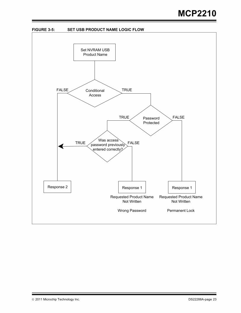
3.1.5 SET USB PRODUCT NAME3.1.5.1 Responses
TABLE 3-14: COMMAND STRUCTUREByte Index Meaning
0 0x60 – Set Chip NVRAM Parameters – command code1 0x40 – Set USB Product Name – sub-command code2 0x00 – Reserved3 0x00 – Reserved4 Total USB String Descriptor Length (this is the length of the Product string multiplied by 2 + 2)
Example: “MCP2210 USB to SPI Master” has 25 Unicode characters.- The value to be filled in is: (25 * 2) + 2 = 52 (decimal) = 0x34
5 USB String Descriptor ID – always fill with 0x036 Unicode Character Low Byte
Example: For the “MCP2210 USB to SPI Master” Unicode string, place here the low byte of the Unicode for character “M”.
- Fill this index with 0x4D7 Unicode Character High Byte
Example: For the “MCP2210 USB to SPI Master” Unicode string, place here the high byte of the Unicode for character “M”.
- Fill this index with 0x008-63 Fill in the remaining Unicode characters in the string
TABLE 3-15: RESPONSE 1 STRUCTUREByte Index Meaning
0 0x60 – Set Chip NVRAM Parameters – echos back the given command code1 0xFB – Blocked Access – The provided password is not matching the one stored in the chip or the
settings are permanently locked.2-63 Don’t Care
TABLE 3-16: RESPONSE 2 STRUCTUREByte Index Meaning
0 0x60 – Set Chip NVRAM Parameters – echos back the given command code1 0x00 – Command Completed Successfully – settings written2 0x40 – Sub-command Echoed Back for Set USB Product Name code
3-63 Don’t Care
DS22288A-page 22 2011 Microchip Technology Inc.
MCP2210
FIGURE 3-5: SET USB PRODUCT NAME LOGIC FLOWSet NVRAM USBProduct Name
TRUE
Requested Product Name Not Written
Wrong Password
FALSE Conditional Access
Password Protected
Response 1
TRUE
TRUE
FALSE
FALSE Was access
password previously entered correctly?
Requested Product Name Not Written
Permanent Lock
Response 1Response 2
2011 Microchip Technology Inc. DS22288A-page 23

MCP2210
3.1.6 GET SPI POWER-UP TRANSFER SETTINGS3.1.6.1 Responses
TABLE 3-17: COMMAND STRUCTUREByte Index Meaning
0 0x61 – Get NVRAM Settings – command code1 0x10 – Get SPI Power-up Transfer Settings – sub-command code2 0x00 – Reserved
3-63 0x00 – Reserved
TABLE 3-18: RESPONSE 1 STRUCTUREByte Index Meaning
0 0x61 – Get NVRAM Settings – echos back the given command code1 0x00 – Command Completed Successfully2 0x10 – Sub-command Echoed Back for Get SPI Power-up Transfer Settings code3 Don’t Care4 Bit Rate (Byte 3) – 32-bit value (Byte 0, Byte 1, Byte 2, Byte 3)
Example: Bit rate = 12,000,000 bps = 00B7 1B00- This byte position will have a value of = 0x00
5 Bit Rate (Byte 2) – 32-bit value (Byte 0, Byte 1, Byte 2, Byte 3)Example: Bit rate = 12,000,000 bps = 00B7 1B00- This byte position will have a value of = 0x1B
6 Bit Rate (Byte 1) – 32-bit value (Byte 0, Byte 1, Byte 2, Byte 3)Example: Bit rate = 12,000,000 bps = 00B7 1B00- This byte position will have a value of = 0xB7
7 Bit Rate (Byte 0) – 32-bit value (Byte 0, Byte 1, Byte 2, Byte 3)Example: Bit rate = 12,000,000 bps = 00B7 1B00- This byte position will have a value of = 0x00
8 Idle Chip Select Value – 16-bit value (low byte): • MSB – – – – – – LSB
CS7 CS6 CS5 CS4 CS3 CS2 CS1 CS09 Idle Chip Select Value – 16-bit value (high byte):
• MSB – – – – – – LSB x x x x x x x CS8
10 Active Chip Select Value – 16-bit value (low byte): • MSB – – – – – – LSB
CS7 CS6 CS5 CS4 CS3 CS2 CS1 CS011 Active Chip Select Value – 16-bit value (high byte):
• MSB – – – – – – LSB x x x x x x x CS8
12 Chip Select to Data Delay (quanta of 100 µs) – 16-bit value (low byte)Example: If a 500 µs delay between the CS being asserted and the first byte of data is required, the
value will be 0x0005.- This byte position will have a value of: 0x05
13 Chip Select to Data Delay (quanta of 100 µs) – 16-bit value (high byte)Example: If a 500 µs delay between the CS being asserted and the first byte of data is required, the
value will be 0x0005.- This byte position will have a value of: 0x00
DS22288A-page 24 2011 Microchip Technology Inc.

MCP2210
FIGURE 3-6: GET SPI POWER-UP TRANSFER SETTINGS LOGIC FLOW
14 Last Data Byte to CS (De-asserted) Delay (quanta of 100 µs) – 16-bit value (low byte)Example: If a 500 µs delay between the last data byte sent and the CS being de-asserted is required,
the value will be 0x0005.- This byte position will have a value of: 0x05
15 Last Data Byte to CS (De-asserted) Delay (quanta of 100 µs) – 16-bit value (high byte)Example: If a 500 µs delay between the last data byte sent and the CS being de-asserted is required,
the value will be 0x0005.- This byte position will have a value of: 0x00
16 Delay Between Subsequent Data Bytes (quanta of 100 µs) – 16-bit value (low byte)Example: If a 500 µs delay between two consecutive data bytes is required, the value will be 0x0005.- This byte position will have a value of: 0x05
17 Delay Between Subsequent Data Bytes (quanta of 100 µs) – 16-bit value (high byte)Example: If a 500 µs delay between two consecutive data bytes is required, the value will be 0x0005.- This byte position will have a value of: 0x00
18 Bytes to Transfer per SPI Transaction – 16-bit value (low byte)Example: If an SPI transaction of 1250 bytes long is required, the corresponding hex value
will be 0x04E2.- This byte position will have a value of: 0xE2
19 Bytes to Transfer per SPI Transaction – 16-bit value (high byte)Example: If an SPI transaction of 1250 bytes long is required, the corresponding hex value
will be 0x04E2- This byte position will have a value of: 0x04
20 SPI Mode• 0x00 – SPI mode 0• 0x01 – SPI mode 1• 0x02 – SPI mode 2• 0x03 – SPI mode 3
21 - 63 Don’t care
TABLE 3-18: RESPONSE 1 STRUCTURE (CONTINUED)Byte Index Meaning
Get NVRAM SPITransfer Settings
Response 1
NVRAM SPI Transfer Settings
Retrieved
2011 Microchip Technology Inc. DS22288A-page 25

MCP2210
3.1.7 GET POWER-UP CHIP SETTINGS3.1.7.1 Responses
TABLE 3-19: COMMAND STRUCTUREByte Index Meaning
0 0x61 – Get NVRAM Settings – command code1 0x20 – Get Power-up Chip Settings – sub-command code2 0x00 – Reserved
3-63 0x00 – Reserved
TABLE 3-20: RESPONSE 1 STRUCTUREByte Index Meaning
0 0x61 – Get NVRAM Settings – echos back the given command code1 0x00 – Command Completed Successfully2 0x20 – Sub-command Echoed Back for Get Power-up Chip Settings code3 Don’t Care4 GP0 Pin Designation
• GPIO = 0x00 • Chip Selects = 0x01 • Dedicated Function pin = 0x02
5 GP1 Pin Designation • GPIO = 0x00 • Chip Selects = 0x01 • Dedicated Function pin = 0x02
6 GP2 Pin Designation • GPIO = 0x00 • Chip Selects = 0x01 • Dedicated Function pin = 0x02
7 GP3 Pin Designation • GPIO = 0x00 • Chip Selects = 0x01 • Dedicated Function pin = 0x02
8 GP4 Pin Designation • GPIO = 0x00 • Chip Selects = 0x01 • Dedicated Function pin = 0x02
9 GP5 Pin Designation • GPIO = 0x00 • Chip Selects = 0x01 • Dedicated Function pin = 0x02
10 GP6 Pin Designation • GPIO = 0x00 • Chip Selects = 0x01 • Dedicated Function pin = 0x02
DS22288A-page 26 2011 Microchip Technology Inc.

MCP2210
11 GP7 Pin Designation • GPIO = 0x00 • Chip Selects = 0x01 • Dedicated Function pin = 0x02
12 GP8 Pin Designation • GPIO = 0x00 • Chip Selects = 0x01 • Dedicated Function pin = 0x02
13 Default GPIO Output – 16-bit value (low byte): • MSB – – – – – – LSB
GP7 GP6 GP5 GP4 GP3 GP2 GP1 GP014 Default GPIO Output – 16-bit value (high byte):
• MSB – – – – – – LSB x x x x x x x GP8
where x = Don’t Care15 Default GPIO Direction – 16-bit value (low byte):
• MSB – – – – – – LSB GP7DIR GP6DIR GP5DIR GP4DIR GP3DIR GP2DIR GP1DIR GP0DIR
16 Default GPIO Direction – 16-bit value (high byte): • MSB – – – – – – LSB
x x x x x x x GP8DIR17 Other Chip Settings – Enable/Disable Wake-up, Interrupt Counting, SPI Bus Release Options
• Bit 7 – Don’t Care• Bit 6 – Don’t Care• Bit 5 – Don’t Care• Bit 4 – Remote Wake-up Enabled/Disabled
- 0 – Remote Wake-up Disabled- 1 – Remote Wake-up Enabled
• Bit 3 – Dedicated Function – Interrupt Pin mode• Bit 2 – Dedicated Function – Interrupt Pin mode• Bit 1 – Dedicated Function – Interrupt Pin mode
- b111 – Reserved- b110 – Reserved- b101 – Reserved- b100 – Count High Pulses- b011 – Count Low Pulses- b010 – Count Rising Edges- b001 – Count Falling Edges- b000 – No Interrupt Counting
• Bit 0 – SPI Bus Release Enable - 0 = SPI Bus is Released Between Transfer- 1 = SPI Bus is not released by the MCP2210 between transfers
18 NVRAM Chip Parameters Access Control• 0x00 – Chip Settings Not Protected• 0x40 – Chip Settings Protected By Password Access• 0x80 – Chip Settings Permanently Locked
19 - 63 Don’t Care
TABLE 3-20: RESPONSE 1 STRUCTURE (CONTINUED)Byte Index Meaning
2011 Microchip Technology Inc. DS22288A-page 27

MCP2210
FIGURE 3-7: GET POWER-UP CHIP SETTINGS LOGIC FLOWGet NVRAMChip Settings
Response 1
NVRAMChip Settings
Retrieved
DS22288A-page 28 2011 Microchip Technology Inc.

MCP2210
3.1.8 GET USB KEY PARAMETERS3.1.8.1 Responses
FIGURE 3-8: GET USB KEY PARAMETERS LOGIC FLOW
TABLE 3-21: COMMAND STRUCTUREByte Index Meaning
0 0x61 – Get NVRAM Settings – command code1 0x30 – Get USB Key Parameters – sub-command code2 0x00 – Reserved
3-63 0x00 – Reserved
TABLE 3-22: RESPONSE 1 STRUCTUREByte Index Meaning
0 0x61 – Get NVRAM Settings – echos back the given command code1 0x00 – Command Completed Successfully2 0x30 – Sub-command Echoed Back for Get USB Key Parameters code
3-11 Don’t care12 VID low byte13 VID high byte14 PID low byte15 PID high byte
16-28 Don’t care29 Chip Power Option (as per USB specs – Chapter 9)
• Bit 7 – Host Powered• Bit 6 – Self Powered• Bit 5 – Remote Wake-up Capable• Bit 4 – Don’t Care• Bit 3 – Don’t Care• Bit 2 – Don’t Care• Bit 1 – Don’t Care• Bit 0 – Don’t Care
30 Requested Current Amount from USB Host (quanta of 2 mA)Example: For 100 mA this byte index will have a value of 50 (in decimal) or 0x32.
31-63 Don’t Care
Get NVRAM USBKey Parameters
Response 1
NVRAM USBKey Parameters
Retrieved
2011 Microchip Technology Inc. DS22288A-page 29

MCP2210
3.1.9 GET USB MANUFACTURER NAME3.1.9.1 Responses
FIGURE 3-9: GET USB MANUFACTURER NAME LOGIC FLOW
TABLE 3-23: COMMAND STRUCTUREByte Index Meaning
0 0x61 – Get NVRAM Settings – command code1 0x50 – Get USB Manufacturer Name – sub-command code2 0x00 – Reserved
3-63 0x00 – Reserved
TABLE 3-24: RESPONSE 1 STRUCTUREByte Index Meaning
0 0x61 – Get NVRAM Settings – echos back the given command code1 0x00 – Command Completed Successfully2 0x50 – Sub-command Echoed Back for Get USB Manufacturer Name code3 Don’t Care4 Total USB String Descriptor Length (this is the length of the Manufacturer string multiplied by 2 + 2)
Example: “Microchip Technology Inc.” has 25 Unicode characters.- The retrieved value is: (25 x 2) + 2 = 52 (decimal) = 0x34
5 USB String Descriptor ID – always 0x036 Unicode Character Low Byte
Example: For the “Microchip Technology Inc.” Unicode string, there will be the low byte of the Unicode for character “M”.
- This byte index will have a value of 0x4D7 Unicode Character High Byte
Example: For the “Microchip Technology Inc.” Unicode string, there will be the high byte of the Unicode for character “M”.
- This byte index will have a value of 0x008-63 Remaining Unicode Characters
Get NVRAM USBManufacturer Name
Response 1
NVRAM USBManufacturer
Name Retrieved
DS22288A-page 30 2011 Microchip Technology Inc.

MCP2210
3.1.10 GET USB PRODUCT NAME3.1.10.1 Responses
FIGURE 3-10: GET USB PRODUCT NAME LOGIC FLOW
TABLE 3-25: COMMAND STRUCTUREByte Index Meaning
0 0x61 – Get NVRAM Settings – command code1 0x40 – Get USB Product Name – sub-command code2 0x00 – Reserved
3-63 0x00 – Reserved
TABLE 3-26: RESPONSE 1 STRUCTUREByte Index Meaning
0 0x61 – Get NVRAM Settings – echos back the given command code1 0x00 – Command Completed Successfully2 0x40 – Sub-command Echoed Back for Get USB Product Name code3 Don’t Care4 Total USB String Descriptor Length (this is the length of the Product string multiplied by 2 + 2)
Example: “MCP2210 USB to SPI Master” has 25 Unicode characters- The retrieved value is: (25 x 2) + 2 = 52 (decimal) = 0x34
5 USB String Descriptor ID – always 0x036 Unicode Character Low byte
Example: For the “MCP2210 USB to SPI Master” Unicode string, there will be the low byte of the Unicode for character “M”.
- This byte index will have a value of 0x4D7 Unicode Character High byte
Example: For the “MCP2210 USB to SPI Master” Unicode string, there will be the high byte of the Unicode for character “M”.
- This byte index will have a value of 0x008-63 Remaining Unicode Characters
Get NVRAM USBProduct Name
Response 1
NVRAM USBProduct Name
Retrieved
2011 Microchip Technology Inc. DS22288A-page 31

MCP2210
3.1.11 SEND ACCESS PASSWORD3.1.11.1 Responses
TABLE 3-27: COMMAND STRUCTUREByte Index Meaning
0 0x70 – SEND ACCESS Password – command code1 0x00 – Reserved2 0x00 – Reserved3 0x00 – Reserved4 Password Character 05 Password Character 16 Password Character 27 Password Character 38 Password Character 49 Password Character 5
10 Password Character 611 Password Character 7
12-63 0x00 – Reserved
TABLE 3-28: RESPONSE 1 STRUCTUREByte Index Meaning
0 0x70 – SEND ACCESS Password – echos back the given command code1 0x00 – Command Completed Successfully – chip settings not protected2 Don’t Care
3-63 Don’t Care
TABLE 3-29: RESPONSE 2 STRUCTUREByte Index Meaning
0 0x70 – SEND ACCESS Password – echos back the given command code1 0xFC – Access Not Allowed – access rejected2 Don’t Care
3-63 Don’t Care
TABLE 3-30: RESPONSE 3 STRUCTUREByte Index Meaning
0 0x70 – SEND ACCESS Password – echos back the given command code1 0xFD – Access Not Allowed – Chip conditional access is on, the password does not match and the
number of attempts is less than the accepted threshold of 5.2 Don’t Care
3-63 Don’t Care
DS22288A-page 32 2011 Microchip Technology Inc.

MCP2210
FIGURE 3-11: SEND ACCESS PASSWORD LOGIC FLOW
TABLE 3-31: RESPONSE 4 STRUCTUREByte Index Meaning
0 0x70 – SEND ACCESS Password – echos back the given command code1 0xFB – Access Not Allowed – Chip conditional access is on, the password does not match and the
number of attempts is above the accepted threshold of 5. The Access Password mechanism is temporarily blocked and no further password access will be accepted until the next power-up.
2 Don’t Care3-63 Don’t Care
TABLE 3-32: RESPONSE 5 STRUCTUREByte Index Meaning
0 0x70 – SEND ACCESS Password – echos back the given command code1 0x00 – Command Completed Successfully – Chip conditional access is on, the supplied password is
matching the one stored in the chip’s NVRAM.2 Don’t Care
3-63 Don’t Care
Send Access Password
FALSE TRUE
FALSE
FALSE
FALSE
TRUE
TRUE
TRUE
Response 1
Response 2
Response 4
Response 3Response 5
Chip SettingsProtectedChip Settings
Not Protected
Access GrantedPermanent Lock
PasswordProtected
PasswordAttempts
< 5
PasswordMatched
Access Granted
Chip Access Rejected
Chip Access Rejected
Chip Access RejectedIncrement
the Number of Attempts
Temporarily Chip Access Lock
2011 Microchip Technology Inc. DS22288A-page 33

MCP2210
3.2 Read/Write RAM SettingsThe set of commands/responses described in this section relates to the manipulation of the RAM settings (volatile).3.2.1 GET (VM) SPI TRANSFER SETTINGS
3.2.1.1 Responses
TABLE 3-33: COMMAND STRUCTUREByte Index Meaning
0 0x41 – Get (VM) SPI Transfer Settings – command code1 0x00 – Reserved2 0x00 – Reserved
3-63 0x00 – Reserved
TABLE 3-34: RESPONSE 1 STRUCTUREByte Index Meaning
0 0x41 – Get SPI Transfer Settings (volatile memory)1 0x00 – Command Completed Successfully2 Size in Bytes of the SPI Transfer Structure: 17 (in decimal) = 0x113 Don’t Care4 Bit Rate (Byte 3) – 32-bit value (Byte 0, Byte 1, Byte 2, Byte 3)
Example: Bit rate = 12,000,000 bps = 00B7 1B00- This byte position will have a value of = 0x00
5 Bit Rate (Byte 2) – 32-bit value (Byte 0, Byte 1, Byte 2, Byte 3)Example: Bit rate = 12,000,000 bps = 00B7 1B00
- This byte position will have a value of = 0x1B6 Bit Rate (Byte 1) – 32-bit value (Byte 0, Byte 1, Byte 2, Byte 3)
Example: Bit rate = 12,000,000 bps = 00B7 1B00- This byte position will have a value of = 0xB7
7 Bit Rate (Byte 0) – 32-bit value (Byte 0, Byte 1, Byte 2, Byte 3)Example: Bit rate = 12,000,000 bps = 00B7 1B00
- This byte position will have a value of = 0x008 Idle Chip Select Value – 16-bit value (low byte):
• MSB – – – – – – LSBCS7 CS6 CS5 CS4 CS3 CS2 CS1 CS0
9 Idle Chip Select Value – 16-bit value (high byte): • MSB – – – – – – LSB
x x x x x x x CS810 Active Chip Select Value – 16-bit value (low byte):
• MSB – – – – – – LSBCS7 CS6 CS5 CS4 CS3 CS2 CS1 CS0
11 Active Chip Select Value – 16-bit value (high byte): • MSB – – – – – – LSB
x x x x x x x CS812 Chip Select to Data Delay (quanta of 100 µs) – 16-bit value (low byte)
Example: If we have 500 µs delay between the CS being asserted and the first byte of data, the value will be 0x0005.
- This byte position will have a value of: 0x05
DS22288A-page 34 2011 Microchip Technology Inc.

MCP2210
FIGURE 3-12: GET (VM) SPI TRANSFER SETTINGS LOGIC FLOW
13 Chip Select to Data Delay (quanta of 100 µs) – 16-bit value (high byte)Example: If we have 500 µs delay between the CS being asserted and the first byte of data, the value
will be 0x0005.- This byte position will have a value of: 0x00
14 Last Data Byte to CS (de-asserted) Delay (quanta of 100 µs) – 16-bit value (low byte)Example: If we have 500 µs delay between the last data byte sent and the CS being de-asserted, the
value will be 0x0005.- This byte position will have a value of: 0x05
15 Last Data Byte to CS (de-asserted) Delay (quanta of 100 µs) – 16-bit value (high byte)Example: If we have 500 µs delay between the last data byte sent and the CS being de-asserted, the
value will be 0x0005.- This byte position will have a value of: 0x00
16 Delay Between Subsequent Data Bytes (quanta of 100 µs) – 16-bit value (low byte)Example: If we have 500 µs delay between two consecutive data bytes, the value will be 0x0005.- This byte position will have a value of: 0x05
17 Delay Between Subsequent Data Bytes (quanta of 100 µs) – 16-bit value (high byte)Example: If we have 500 µs delay between two consecutive data bytes, the value will be 0x0005.
- This byte position will have a value of: 0x0018 Bytes to Transfer per SPI Transaction – 16-bit value (low byte)
Example: If an SPI transaction of 1250 bytes long is required, the corresponding hex value will be 0x04E2.
- This byte position will have a value of: 0xE219 Bytes to Transfer per SPI Transaction – 16-bit value (high byte)
Example: If an SPI transaction of 1250 bytes long is required, the corresponding hex value will be 0x04E2.
- This byte position will have a value of: 0x0420 SPI Mode
• 0x00 – SPI mode 0• 0x01 – SPI mode 1• 0x02 – SPI mode 2• 0x03 – SPI mode 3
21 - 63 Don’t Care
TABLE 3-34: RESPONSE 1 STRUCTUREByte Index Meaning
Get RAM SPITransfer Settings
Response 1
RAM SPITransfer Settings
Retrieved
2011 Microchip Technology Inc. DS22288A-page 35

MCP2210
3.2.2 SET (VM) SPI TRANSFER SETTINGSTABLE 3-35: COMMAND 1 STRUCTUREByte Index Meaning
0 0x40 – Set (VM) SPI Transfer Settings (volatile memory)1 0x00 – Reserved2 0x00 – Reserved3 0x00 – Reserved4 Bit Rate (Byte 3) – 32-bit value (Byte 0, Byte 1, Byte 2, Byte 3)
Example: Bit rate = 12,000,000 bps = 00B7 1B00- This byte position will have a value of = 0x00
5 Bit Rate (Byte 2) – 32-bit value (Byte 0, Byte 1, Byte 2, Byte 3)Example: Bit rate = 12,000,000 bps = 00B7 1B00
- This byte position will have a value of = 0x1B6 Bit Rate (Byte 1) – 32-bit value (Byte 0, Byte 1, Byte 2, Byte 3)
Example: Bit rate = 12,000,000 bps = 00B7 1B00- This byte position will have a value of = 0xB7
7 Bit Rate (Byte 0) – 32-bit value (Byte 0, Byte 1, Byte 2, Byte 3)Example: Bit rate = 12,000,000 bps = 00B7 1B00
- This byte position will have a value of = 0x008 Idle Chip Select Value – 16-bit value (low byte):
• MSB – – – – – – LSBCS7 CS6 CS5 CS4 CS3 CS2 CS1 CS0
9 Idle Chip Select Value – 16-bit value (high byte): • MSB – – – – – – LSB
x x x x x x x CS810 Active Chip Select Value – 16-bit value (low byte):
• MSB – – – – – – LSBCS7 CS6 CS5 CS4 CS3 CS2 CS1 CS0
11 Active Chip Select Value – 16-bit value (high byte): • MSB – – – – – – LSB
x x x x x x x CS812 Chip Select to Data Delay (quanta of 100 µs) – 16-bit value (low byte)
Example: If we have 500 µs delay between the CS being asserted and the first byte of data, the value will be 0x0005.
- This byte position will have a value of: 0x0513 Chip Select to Data Delay (quanta of 100 µs) – 16-bit value (high byte)
Example: If a 500 µs delay between the CS being asserted and the first byte of data is required, the value will be 0x0005.
- This byte position will have a value of: 0x0014 Last Data Byte to CS (de-asserted) Delay (quanta of 100 µs) – 16-bit value (low byte)
Example: If a 500 µs delay between the last data byte sent and the CS being asserted is required, the value will be 0x0005.
- This byte position will have a value of: 0x0515 Last Data Byte to CS (de-asserted) Delay (quanta of 100 µs) – 16-bit value (high byte)
Example: If a 500 µs delay between the last data byte sent and the CS being de-asserted is required, the value will be 0x0005.
- This byte position will have a value of: 0x00
DS22288A-page 36 2011 Microchip Technology Inc.

MCP2210
3.2.2.1 Responses
16 Delay Between Subsequent Data Bytes (quanta of 100 µs) – 16-bit value (low byte)Example: If a 500 µs delay between two consecutive data bytes is required, the value will be 0x0005.- This byte position will have a value of: 0x05
17 Delay Between Subsequent Data Bytes (quanta of 100 µs) – 16-bit value (high byte)Example: If a 500 µs delay between two consecutive data bytes is required, the value will be 0x0005.
- This byte position will have a value of: 0x0018 Bytes to Transfer per SPI Transaction – 16-bit value (low byte)
Example: If an SPI transaction of 1250 bytes long is required, the corresponding hex value will be 0x04E2.
- This byte position will have a value of: 0xE219 Bytes to Transfer per SPI Transaction – 16-bit value (high byte)
Example: If an SPI transaction of 1250 bytes long is required, the corresponding hex value will be 0x04E2.
- This byte position will have a value of: 0x0420 SPI Mode
• 0x00 – SPI mode 0• 0x01 – SPI mode 1• 0x02 – SPI mode 2• 0x03 – SPI mode 3
21-63 Don’t care
TABLE 3-35: COMMAND 1 STRUCTURE (CONTINUED)Byte Index Meaning
TABLE 3-36: RESPONSE 1 STRUCTUREByte Index Meaning
0 0x40 – Echoes back the completed command for Set (VM) SPI Transfer Settings code1 0x00 – Command Completed Successfully2 Don’t Care3 Don’t Care4 Bit Rate (Byte 3) – 32-bit value (Byte 0, Byte 1, Byte 2, Byte 3)
Example: Bit rate = 12,000,000 bps = 00B7 1B00- This byte position will have a value of = 0x00
5 Bit Rate (Byte 2) – 32-bit value (Byte 0, Byte 1, Byte 2, Byte 3)Example: Bit rate = 12,000,000 bps = 00B7 1B00
- This byte position will have a value of = 0x1B6 Bit Rate (Byte 1) – 32-bit value (Byte 0, Byte 1, Byte 2, Byte 3)
Example: Bit rate = 12,000,000 bps = 00B7 1B00- This byte position will have a value of = 0xB7
7 Bit Rate (Byte 0) – 32-bit value (Byte 0, Byte 1, Byte 2, Byte 3)Example: Bit rate = 12,000,000 bps = 00B7 1B00
- This byte position will have a value of = 0x008 Idle Chip Select Value – 16-bit value (low byte):
• MSB – – – – – – LSBCS7 CS6 CS5 CS4 CS3 CS2 CS1 CS0
9 Idle Chip Select Value – 16-bit value (high byte): • MSB – – – – – – LSB
x x x x x x x CS8
2011 Microchip Technology Inc. DS22288A-page 37

MCP2210
10 Active Chip Select Value – 16-bit value (low byte): • MSB – – – – – – LSB
CS7 CS6 CS5 CS4 CS3 CS2 CS1 CS011 Active Chip Select Value – 16-bit value (high byte):
• MSB – – – – – – LSB x x x x x x x CS8
12 Chip Select to Data Delay (quanta of 100 µs) – 16-bit value (low byte)Example: If we have 500 µs delay between the CS being asserted and the first byte of data, the
value will be 0x0005.- This byte position will have a value of: 0x05
13 Chip Select to Data Delay (quanta of 100 µs) – 16-bit value (high byte)Example: If we have 500 µs delay between the CS being asserted and the first byte of data, the
value will be 0x0005.- This byte position will have a value of: 0x00
14 Last Data Byte to CS (de-asserted) Delay (quanta of 100 µs) – 16-bit value (low byte)Example: If we have 500 µs delay between the last data byte sent and the CS being de-asserted,
the value will be 0x0005.- This byte position will have a value of: 0x05
15 Last Data Byte to CS (de-asserted) Delay (quanta of 100 µs) – 16-bit value (high byte)Example: If we have 500 µs delay between the last data byte sent and the CS being de-asserted,
the value will be 0x0005.- This byte position will have a value of: 0x00
16 Delay Between Subsequent Data Bytes (quanta of 100 µs) – 16-bit value (low byte)Example: If we have 500 µs delay between two consecutive data bytes, the value will be 0x0005.- This byte position will have a value of: 0x05
17 Delay Between Subsequent Data Bytes (quanta of 100 µs) – 16-bit value (low byte)Example: If we have 500 µs delay between two consecutive data bytes, the value will be 0x0005.- This byte position will have a value of: 0x00
18 Bytes to Transfer per SPI Transaction – 16-bit value (low byte)Example: If an SPI transaction of 1250 bytes long is required, the corresponding hex value
will be 0x04E2.- This byte position will have a value of: 0xE2
19 Bytes to Transfer per SPI Transaction – 16-bit value (high byte)Example: If an SPI transaction of 1250 bytes long is required, the corresponding hex value
will be 0x04E2.- This byte position will have a value of: 0x04
20 SPI Mode• 0x00 – SPI mode 0• 0x01 – SPI mode 1• 0x02 – SPI mode 2• 0x03 – SPI mode 3
21 - 63 Don’t Care
TABLE 3-36: RESPONSE 1 STRUCTURE (CONTINUED)Byte Index Meaning
DS22288A-page 38 2011 Microchip Technology Inc.

MCP2210
FIGURE 3-13: SET (VM) SPI TRANSFER SETTINGS LOGIC FLOW
3.2.3 GET (VM) CURRENT CHIP SETTINGS
TABLE 3-37: RESPONSE 2 STRUCTUREByte Index Meaning
0 0x40 – Set (VM) SPI Transfer Settings – echos back the given command code1 0xF8 – USB transfer in progress – Settings not written2 Don’t Care
3-63 Don’t Care
TABLE 3-38: COMMAND STRUCTUREByte Index Meaning
0 0x20 – Get (VM) GPIO Current Chip Settings1 0x00 – Reserved2 0x00 – Reserved
3-63 0x00 – Reserved
Set RAM SPITransfer Settings
Response 2
TRUEFALSE
Response 1
Requested RAM SPISettings Not Written
SPI TransferOngoing
2011 Microchip Technology Inc. DS22288A-page 39

MCP2210
3.2.3.1 ResponsesTABLE 3-39: RESPONSE 1 STRUCTUREByte Index Meaning
0 0x20 – Get (VM) GPIO Current Chip Settings – echos back the given command code1 0x00 – Command Completed Successfully2 Don’t Care3 Don’t Care4 GP0 Pin Designation
• GPIO = 0x00 • Chip Selects = 0x01• Dedicated Function pin = 0x02
5 GP1 Pin Designation • GPIO = 0x00 • Chip Selects = 0x01• Dedicated Function pin = 0x02
6 GP2 Pin Designation • GPIO = 0x00 • Chip Selects = 0x01• Dedicated Function pin = 0x02
7 GP3 Pin Designation • GPIO = 0x00 • Chip Selects = 0x01• Dedicated Function pin = 0x02
8 GP4 Pin Designation • GPIO = 0x00 • Chip Selects = 0x01• Dedicated Function pin = 0x02
9 GP5 Pin Designation • GPIO = 0x00 • Chip Selects = 0x01• Dedicated Function pin = 0x02
10 GP6 Pin Designation • GPIO = 0x00 • Chip Selects = 0x01• Dedicated Function pin = 0x02
11 GP7 Pin Designation • GPIO = 0x00 • Chip Selects = 0x01• Dedicated Function pin = 0x02
12 GP8 Pin Designation • GPIO = 0x00 • Chip Selects = 0x01• Dedicated Function pin = 0x02
13 Default GPIO Output – 16-bit value (low byte): • MSB – – – – – – LSB
GP7 GP6 GP5 GP4 GP3 GP2 GP1 GP0
DS22288A-page 40 2011 Microchip Technology Inc.

MCP2210
14 Default GPIO Output – 16-bit value (high byte):• MSB – – – – – – LSB
x x x x x x x GP8
where x = Don’t Care15 Default GPIO Direction – 16-bit value (low byte):
• MSB – – – – – – LSBGP7DIR GP6DIR GP5DIR GP4DIR GP3DIR GP2DIR GP1DIR GP0DIR
16 Default GPIO Direction – 16-bit value (high byte): • MSB – – – – – – LSB
x x x x x x x GP8DIR17 Other Chip Settings – Enable/Disable Wake-up, Interrupt Counting, SPI Bus Release Options
• Bit 7 – Don’t Care• Bit 6 – Don’t Care• Bit 5 – Don’t Care• Bit 4 – Remote Wake-up Enabled/Disabled
- 0 – Remote Wake-up Disabled- 1 – Remote Wake-up Enabled
• Bit 3 – Dedicated Function – Interrupt Pin mode• Bit 2 – Dedicated Function – Interrupt Pin mode• Bit 1 – Dedicated Function – Interrupt Pin mode
- b111 – Reserved- b110 – Reserved- b101 – Reserved- b100 – Count High Pulses- b011 – Count Low Pulses- b100 – Count High Pulses- b011 – Count Low Pulses- b010 – Count Rising Edges- b001 – Count Falling Edges- b000 – No Interrupt Counting
• Bit 0 – SPI Bus Release Enable - 0 = SPI Bus is Released between transfer- 1 = SPI Bus is Not Released by the MCP2210 between transfers
18 NVRAM Chip Parameters Access Control• 0x00 – Chip settings not protected• 0x40 – Chip settings protected by password access• 0x80 – Chip settings permanently locked
19-63 Don’t Care
TABLE 3-39: RESPONSE 1 STRUCTURE (CONTINUED)Byte Index Meaning
2011 Microchip Technology Inc. DS22288A-page 41

MCP2210
FIGURE 3-14: GET (VM) CURRENT CHIP SETTINGS LOGIC FLOW3.2.4 SET (VM) CURRENT CHIP SETTINGS
TABLE 3-40: COMMAND STRUCTUREByte Index Meaning
0 0x21 – Set (VM) Current Chip Settings1 0x00 – Reserved2 0x00 – Reserved3 0x00 – Reserved4 GP0 Pin Designation
• GPIO = 0x00 • Chip Selects = 0x01• Dedicated Function pin = 0x02
5 GP1 Pin Designation • GPIO = 0x00 • Chip Selects = 0x01• Dedicated Function pin = 0x02
6 GP2 Pin Designation • GPIO = 0x00 • Chip Selects = 0x01• Dedicated Function pin = 0x02
7 GP3 Pin Designation • GPIO = 0x00 • Chip Selects = 0x01• Dedicated Function pin = 0x02
8 GP4 Pin Designation • GPIO = 0x00 • Chip Selects = 0x01• Dedicated Function pin = 0x02
Get RAM Chip Settings
Response 1
RAM Chip Settings
Retrieved
DS22288A-page 42 2011 Microchip Technology Inc.

MCP2210
9 GP5 Pin Designation • GPIO = 0x00 • Chip Selects = 0x01• Dedicated Function pin = 0x02
10 GP6 Pin Designation • GPIO = 0x00 • Chip Selects = 0x01• Dedicated Function pin = 0x02
11 GP7 Pin Designation • GPIO = 0x00 • Chip Selects = 0x01• Dedicated Function pin = 0x02
12 GP8 Pin Designation • GPIO = 0x00 • Chip Selects = 0x01• Dedicated Function pin = 0x02
13 Default GPIO Output – 16-bit value (low byte): • MSB – – – – – – LSB
GP7 GP6 GP5 GP4 GP3 GP2 GP1 GP014 Default GPIO Output – 16-bit value (high byte):
• MSB – – – – – – LSB x x x x x x x GP8
where x = Don’t Care15 Default GPIO Direction – 16-bit value (low byte):
• MSB – – – – – – LSBGP7DIR GP6DIR GP5DIR GP4DIR GP3DIR GP2DIR GP1DIR GP0DIR
16 Default GPIO Direction – 16-bit value (high byte): • MSB – – – – – – LSB
x x x x x x x GP8DIR
TABLE 3-40: COMMAND STRUCTURE (CONTINUED)Byte Index Meaning
2011 Microchip Technology Inc. DS22288A-page 43

MCP2210
17 Other Chip Settings – Enable/Disable Wake-up, Interrupt Counting, SPI Bus Release Options• Bit 7 – Don’t Care• Bit 6 – Don’t Care• Bit 5 – Don’t Care• Bit 4 – Remote Wake-up Enabled/Disabled
- 0 – Remote Wake-up Disabled- 1 – Remote Wake-up Enabled
• Bit 3 – Dedicated Function – Interrupt Pin mode• Bit 2 – Dedicated Function – Interrupt Pin mode• Bit 1 – Dedicated Function – Interrupt Pin mode
- b111 – Reserved- b110 – Reserved- b101 – Reserved- b100 – Count High Pulses- b011 – Count Low Pulses- b100 – Count High Pulses- b011 – Count Low Pulses- b010 – Count Rising Edges- b001 – Count Falling Edges- b000 – No Interrupt Counting
• Bit 0 – SPI Bus Release Enable - 0 = SPI Bus is Released between transfer- 1 = SPI Bus is Not Released by the MCP2210 between transfers
18-63 Reserved (fill in with 0x00)
TABLE 3-40: COMMAND STRUCTURE (CONTINUED)Byte Index Meaning
DS22288A-page 44 2011 Microchip Technology Inc.

MCP2210
FIGURE 3-15: SET (VM) CURRENT CHIP SETTINGS LOGIC FLOW
TABLE 3-41: RESPONSE 1 STRUCTUREByte Index Meaning
0 0x21 – Set (VM) Current Chip Settings – echos back the given command code1 0x00 – Command Completed Successfully2 Don’t Care
3-63 Don’t Care
Set RAM Chip Settings
Response 1
RAM Chip Settings Written
2011 Microchip Technology Inc. DS22288A-page 45

MCP2210
3.2.5 GET (VM) GPIO CURRENT PIN DIRECTION3.2.5.1 Responses
FIGURE 3-16: GET (VM) GPIO CURRENT PIN DIRECTION LOGIC FLOW
TABLE 3-42: COMMAND STRUCTUREByte Index Meaning
0 0x33 – Get (VM) GPIO Current Pin Direction1 0x00 – Reserved2 0x00 – Reserved
3-63 0x00 – Reserved
TABLE 3-43: RESPONSE 1 STRUCTUREByte Index Meaning
0 0x33 – Get (VM) GPIO Current Pin Direction – echos back the given command code1 0x00 – Command Completed Successfully2 Don’t Care3 Don’t Care4 GPIO Direction – 16-bit value (low byte):
• MSB – – – – – – LSBGP7DIR GP6DIR GP5DIR GP4DIR GP3DIR GP2DIR GP1DIR GP0DIR
5 GPIO Direction – 16-bit value (high byte): • MSB – – – – – – LSB
x x x x x x x GP8DIR6-63 Don’t Care
Note 1: This command will only have an effect on those GPs previously configured as GPIOs.
Get RAM GPIO Direction
Response 1
RAM GPIODirection Retrieved
DS22288A-page 46 2011 Microchip Technology Inc.

MCP2210
3.2.6 SET (VM) GPIO CURRENT PIN DIRECTION3.2.6.1 Responses
FIGURE 3-17: SET (VM) GPIO CURRENT PIN DIRECTION LOGIC FLOW
TABLE 3-44: COMMAND STRUCTUREByte Index Meaning
0 0x32 – Set (VM) GPIO Current Pin Direction1 0x00 – Reserved2 0x00 – Reserved3 0x00 – Reserved4 GPIO Direction – 16-bit value (low byte):
• MSB – – – – – – LSBGP7DIR GP6DIR GP5DIR GP4DIR GP3DIR GP2DIR GP1DIR GP0DIR
5 GPIO Direction – 16-bit value (high byte): • MSB – – – – – – LSB
x x x x x x x GP8DIR6-63 0x00 – Reserved
TABLE 3-45: RESPONSE 1 STRUCTUREByte Index Meaning
0 0x32 – Set (VM) GPIO Current Pin Direction – echos back the given command code1 0x00 – Command Completed Successfully2 Don’t Care
3-63 Don’t Care
Set RAM GPIO Direction
Response 1
RAM GPIODirection Written
2011 Microchip Technology Inc. DS22288A-page 47

MCP2210
3.2.7 GET GPIO CURRENT PIN VALUE3.2.7.1 Responses
FIGURE 3-18: GET GPIO CURRENT PIN VALUE LOGIC FLOW
TABLE 3-46: COMMAND STRUCTUREByte Index Meaning
0 0x31 – Get (VM) GPIO Current Pin Value1 0x00 – Reserved2 0x00 – Reserved
3-63 0x00 – Reserved
TABLE 3-47: RESPONSE 1 STRUCTUREByte Index Meaning
0 0x31 – Get (VM) GPIO Current Pin Value – echos back the given command code1 0x00 – Command Completed Successfully2 Don’t Care3 Don’t Care4 GPIO Pin Value – 16-bit value (low byte):
• MSB – – – – – – LSBGP7VAL GP6VAL GP5VAL GP4VAL GP3VAL GP2VAL GP1VAL GP0VAL
5 GPIO Pin Value – 16-bit value (high byte): • MSB – – – – – – LSB
x x x x x x x GP8VAL6-63 Don’t Care
Note 1: This command will only have an effect on those GPs previously assigned to a GPIO functionality.
Get RAM GPIO Value
Response 1
RAM GPIOValue Retrieved
DS22288A-page 48 2011 Microchip Technology Inc.

MCP2210
3.2.8 SET GPIO CURRENT PIN VALUE3.2.8.1 Responses
FIGURE 3-19: SET GPIO CURRENT PIN VALUE LOGIC FLOW
TABLE 3-48: COMMAND STRUCTUREByte Index Meaning
0 0x30 – Set (VM) GPIO Current Pin Value 1 0x00 – Reserved2 0x00 – Reserved3 0x00 – Reserved4 GPIO Pin Value – 16-bit value (low byte):
• MSB – – – – – – LSBGP7VAL GP6VAL GP5VAL GP4VAL GP3VAL GP2VAL GP1VAL GP0VAL
5 GPIO Pin Value – 16-bit value (high byte): • MSB – – – – – – LSB
x x x x x x x GP8VAL6-63 0x00 – Reserved
Note 1: The GPIO pin value will have an effect only on those GPs previously configured as GPIOs.
TABLE 3-49: RESPONSE 1 STRUCTUREByte Index Meaning
0 0x30 – Set (VM) GPIO Current Pin Value – echos back the given command code1 0x00 - Command Completed Successfully2 Don’t Care3 Don’t Care4 Read Back Actual GPIO Pin Value – 16-bit value (low byte):
• MSB – – – – – – LSBGP7VAL GP6VAL GP5VAL GP4VAL GP3VAL GP2VAL GP1VAL GP0VAL
5 Read Back Actual GPIO Pin Value – 16-bit value (high byte): • MSB – – – – – – LSB
x x x x x x x GP8VAL6-63 Don’t Care
Set RAM GPIO Output Value
Response 1
RAM GPIOOutput Value
Written
2011 Microchip Technology Inc. DS22288A-page 49

MCP2210
3.3 Read/Write EEPROM MemoryThis set of commands/responses described in this section relates to the manipulation of the EEPROM memory.3.3.1 READ EEPROM MEMORY
3.3.1.1 Responses
FIGURE 3-20: READ EEPROM MEMORY LOGIC FLOW
TABLE 3-50: COMMAND STRUCTUREByte Index Meaning
0 0x50 – READ EEPROM Memory – command code 1 EEPROM Memory Address to be read2 0x00 – Reserved
3-63 0x00 – Reserved
TABLE 3-51: RESPONSE 1 STRUCTUREByte Index Meaning
0 0x50 – READ EEPROM Memory – echos back the given command code1 0x00 – Command Completed Successfully2 EEPROM Memory Address3 EEPROM Memory content at the requested address
4-63 Don’t Care
Read EEPROMMemory Location
Response 1
EEPROM Memory Location Content Retrieved
DS22288A-page 50 2011 Microchip Technology Inc.

MCP2210
3.3.2 WRITE EEPROM MEMORY3.3.2.1 Responses
TABLE 3-52: COMMAND STRUCTUREByte Index Meaning
0 0x51 – WRITE EEPROM Memory – command code 1 EEPROM Memory Address to be written2 The value to be written to at the given address
3-63 0x00 – Reserved
TABLE 3-53: RESPONSE 1 STRUCTUREByte Index Meaning
0 0x51 – WRITE EEPROM Memory – echos back the given command code1 0x00 – Command Completed Successfully2 Don’t Care
3-63 Don’t Care
TABLE 3-54: RESPONSE 2 STRUCTUREByte Index Meaning
0 0x51 – WRITE EEPROM Memory – echos back the given command code1 0xFA – EEPROM Write Failure2 Don’t Care
3-63 Don’t Care
TABLE 3-55: RESPONSE 3 STRUCTUREByte Index Meaning
0 0x51 – WRITE EEPROM Memory – echos back the given command code1 0xFB – EEPROM is password protected or permanently locked2 Don’t Care
3-63 Don’t Care
2011 Microchip Technology Inc. DS22288A-page 51

MCP2210
FIGURE 3-21: WRITE EEPROM MEMORY LOGIC FLOWFALSE TRUE
FALSE
FALSE
FALSETRUE
TRUE
TRUE
Response 1 Response 2
Response 3
Response 3
Write EEPROMMemory Location
Conditional Access
PasswordProtected
Was access password previously entered correctly?
EEPROMWrite Failure
Permanent Lock
Requested EEPROMMemory Location
Not Written
Wrong Password
Requested EEPROMMemory Location
Not Written
Requested NVRAM SPI Settings Not Written
EEPROMMemory Location
Written
DS22288A-page 52 2011 Microchip Technology Inc.

MCP2210
3.4 External Interrupt Pin (GP6) Event StatusThe External Interrupt pin event status command is used by the USB host to query the external interrupt events recordedby the MCP2210. In order to have the MCP2210 record the number of external interrupt events, GP6 must be configuredto have its dedicated function active.3.4.1 GET (VM) THE CURRENT NUMBER OF EVENTS FROM THE INTERRUPT PIN
3.4.1.1 Responses
FIGURE 3-22: GET (VM) THE CURRENT NUMBER OF EVENTS FROM THE INTERRUPT PIN LOGIC FLOW
TABLE 3-56: COMMAND STRUCTUREByte Index Meaning
0 0x12 – Get (VM) the Current Number of Events From the Interrupt Pin 1 Reset or Not the Event Counter
• 0x00 – reads, then resets the event counter• Any other value – the event counter is read, however, the counter is not reset
2-63 0x00 - Reserved
TABLE 3-57: RESPONSE 1 STRUCTUREByte Index Meaning
0 0x12 – Get (VM) the Current Number of Events from the Interrupt Pin – echos back the given command code
1 0x00 – Command Completed Successfully2 Don’t Care3 Don’t Care4 Interrupt Event Counter – 16-bit value (low byte)5 Interrupt Event Counter – 16-bit value (high byte)
63-63 Don’t Care
Get External Interrupt Pin Events
Counter
Response 1
External InterruptPin Event CounterValue Retrieved
2011 Microchip Technology Inc. DS22288A-page 53

MCP2210
3.5 SPI Data TransferThe set of commands/responses described in this section relates to the SPI data transfer functionality.3.5.1 TRANSFER SPI DATA
3.5.1.1 Responses
TABLE 3-58: COMMAND STRUCTUREByte Index Meaning
0 0x42 – Transfer SPI Data – command code 1 The number of bytes to be transferred in this packet (from 0 to 60 inclusively)2 0x00 – Reserved3 0x00 – Reserved
4-63 The SPI Data to be sent on the data transfer
TABLE 3-59: RESPONSE 1 STRUCTUREByte Index Meaning
0 0x42 – Transfer SPI Data – echos back the given command code1 0xF7 – SPI Data Not Accepted – SPI bus not available (the external owner has control over it)2 Don’t Care
3-63 Don’t Care
TABLE 3-60: RESPONSES 2 STRUCTUREByte Index Meaning
0 0x42 – Transfer SPI Data – echos back the given command code1 0x00 – SPI Data accepted – Command Completed Successfully – SPI data accepted2 How many SPI received data bytes the chip is sending back to the host3 SPI Transfer Engine Status
• 0x20 – SPI transfer started – no data to receive4-63 SPI Received Data Bytes. The number of data bytes is specified at byte index 2
TABLE 3-61: RESPONSE 3 STRUCTUREByte Index Meaning
0 0x42 – Transfer SPI Data – echos back the given command code1 0xF8 – SPI Data Not Accepted – SPI transfer in progress – cannot accept any data for the moment2 Don’t Care
3-63 Don’t Care
DS22288A-page 54 2011 Microchip Technology Inc.

MCP2210
FIGURE 3-23: TRANSFER SPI DATA LOGIC FLOW
TABLE 3-62: RESPONSE 4 STRUCTUREByte Index Meaning
0 0x42 – Transfer SPI Data – echos back the given command code1 0x00 – SPI Data accepted – Command Completed Successfully – SPI data accepted2 How many SPI received data bytes the chip is sending back to the host3 0x30 – SPI Transfer Engine Status: SPI transfer not finished; received data available
4-63 SPI received data bytes. The number of data bytes is specified at byte index 2
TABLE 3-63: RESPONSE 5 STRUCTUREByte Index Meaning
0 0x42 – Transfer SPI Data – echos back the given command code1 0x00 – SPI Data accepted – Command Completed Successfully – SPI data accepted2 How many SPI received data bytes the chip is sending back to the host3 0x10 – SPI Transfer Engine Status: SPI transfer finished – no more data to send
4-63 SPI received data bytes. The number of data bytes is specified at byte index 2
Transfer SPI Data
FALSETRUE
TRUE
TRUE
TRUE
FALSE
FALSE
FALSE
OngoingSPI Transfer
Response 1 Response 2
Response 3Response 5
Response 4
SPI Busused by External Master
SPI Bus ownedby an External Master
SPI Data AcceptedThe SPI Transfer
will start afterwards
SPI Transfer Ended
SPI TransferWaiting for More Data
SPI Engine waitingfor more data packets
to complete the SPI Transfer
SPI Transfer EndedThe response will contain the last received SPI data packet of the SPI Transfer
Ongoing SPI Transfercannot accept any data now
2011 Microchip Technology Inc. DS22288A-page 55

MCP2210
3.5.2 CANCEL THE CURRENT SPI TRANSFER3.5.2.1 Responses
FIGURE 3-24: CANCEL THE CURRENT SPI TRANSFER LOGIC FLOW
TABLE 3-64: COMMAND STRUCTUREByte Index Meaning
0 0x11 – CANCEL the current SPI transfer – command code1 0x00 – Reserved2 0x00 – Reserved
3-63 0x00 – Reserved
TABLE 3-65: RESPONSE 1 STRUCTUREByte Index Meaning
0 0x11 – CANCEL the current SPI transfer – echos back the given command code1 0x00 – Command Completed Successfully2 SPI Bus Release External Request Status
• 0x01 – No External Request for SPI Bus Release• 0x00 – Pending External Request for SPI Bus Release
3 SPI Bus Current Owner• 0x00 – No Owner• 0x01 – USB Bridge• 0x02 – External Master
4 Attempted Password Accesses – informs the USB host on how many times the NVRAM password was tried
5 Password Guessed• 0x00 – Password Not Guessed• 0x01 – Password Guessed
6-63 Don’t Care
Cancel CurrentSPI Transfer
Response 1
SPI TransferCancelled
DS22288A-page 56 2011 Microchip Technology Inc.

MCP2210
3.5.3 REQUEST SPI BUS RELEASE3.5.3.1 Responses
TABLE 3-66: COMMAND STRUCTUREByte Index Meaning
0 0x80 – Request SPI bus Release – command code 1 The value of the SPI Bus Release ACK pin (only if GP7 is assigned to this dedicated function)2 0x00 – Reserved
3-63 0x00 – Reserved
TABLE 3-67: RESPONSE 1 STRUCTUREByte Index Meaning
0 0x80 – Request SPI bus Release – echos back the given command code1 0x00 – Command Completed Successfully – SPI bus released2 Don’t Care
3-63 Don’t Care
TABLE 3-68: RESPONSES 2 STRUCTUREByte Index Meaning
0 0x80 – Request SPI bus Release – echos back the given command code1 0xF8 – SPI Bus Not Released – SPI transfer in process2 Don’t Care
3-63 Don’t Care
2011 Microchip Technology Inc. DS22288A-page 57

MCP2210
FIGURE 3-25: REQUEST SPI BUS RELEASE LOGIC FLOWRequest SPI Bus Release
SPI TransferOngoing
FALSETRUE
Response 2 Response 1
SPI Bus ReleaseAccepted
SPI Bus Release Not AcceptedSPI Transfer Ongoing
DS22288A-page 58 2011 Microchip Technology Inc.

MCP2210
3.6 Chip StatusThe chip status command is used to retrieve status information regarding the state of the SPI transfer engine.3.6.1 GET MCP2210 STATUS
3.6.1.1 Responses
FIGURE 3-26: GET MCP2210 STATUS LOGIC FLOW
TABLE 3-69: COMMAND STRUCTUREByte Index Meaning
0 0x10 – Get MCP2210 Status – command code1 0x00 – Reserved2 0x00 – Reserved
3-63 0x00 – Reserved
TABLE 3-70: RESPONSE 1 STRUCTUREByte Index Meaning
0 0x10 – Get MCP2210 Status – echos back the given command code1 0x00 – Command Completed Successfully2 SPI Bus Release External Request Status
• 0x01 – No External Request for SPI Bus Release• 0x00 – Pending External Request for SPI Bus Release
3 SPI Bus Current Owner• 0x00 – No Owner• 0x01 – USB Bridge• 0x02 – External Master
4 Attempted Password Accesses – informs the USB host on how many times the NVRAM password was tried
5 Password Guessed• 0x00 – Password Not Guessed• 0x01 – Password Guessed
6-63 Don’t Care
Get MCP2210Status
Response 1
MCP2210 StatusInformation Retrieved
2011 Microchip Technology Inc. DS22288A-page 59

MCP2210
3.6.2 UNSUPPORTED COMMAND CODES3.6.2.1 Responses
TABLE 3-71: COMMAND STRUCTUREByte Index Meaning
0 Usupported Command Code1 Don’t Care
2-63 Don’t Care
TABLE 3-72: RESPONSE 1 STRUCTUREByte Index Meaning
0 Unsupported Command Code Sent – echos back the given command code1 0xF9 – Unknown Command – No effect
2-63 Don’t Care
DS22288A-page 60 2011 Microchip Technology Inc.

MCP2210
NOTES:2011 Microchip Technology Inc. DS22288A-page 61

MCP2210
4.0 ELECTRICAL CHARACTERISTICS
Absolute Maximum Ratings (†) Ambient temperature under bias ......................................................................................................... -40°C to +85°C
Storage temperature ........................................................................................................................ -65°C to +150°C
Voltage on VDD with respect to VSS ................................................................................................... -0.3V to +6.0V
Voltage on MCLR with respect to Vss ................................................................................................. -0.3V to +9.0V
Voltage on VUSB pin with respect to VSS ............................................................................................ -0.3V to +4.0V
Voltage on D+ and D- pins with respect to VSS ...................................................................... -0.3V to (VUSB + 0.3V)
Voltage on all other pins with respect to VSS ............................................................................ -0.3V to (VDD + 0.3V)
Total power dissipation(1) ...............................................................................................................................800 mW
Maximum current out of VSS pin ...................................................................................................................... 95 mA
Maximum current into VDD pin ......................................................................................................................... 95 mA
Clamp current, IK (VPIN < 0 or VPIN > VDD)20 mA
Maximum output current sunk by any I/O pin....................................................................................................25 mA
Maximum output current sourced by any I/O pin...............................................................................................25 mA
Maximum current sunk by all ports....................................................................................................................90 mA
Maximum current sourced by all ports ............................................................................................................. 90 mA
Note 1: Power dissipation is calculated as follows: PDIS = VDD x {IDD – IOH} + {(VDD – VOH) x IOH} + (VOl x IOL).2: VUSB must always be VDD + 0.3V
† NOTICE: Stresses above those listed under “Absolute Maximum Ratings” may cause permanent damage to the device. This is a stress rating only and functional operation of the device at those or any other conditions above those indicated in the operation listings of this specification is not implied. Exposure above maximum rating conditions for extended periods may affect device reliability.
DS22288A-page 62 2011 Microchip Technology Inc.

MCP2210
4.1 DC CHARACTERISTICSDC Characteristics Operating Conditions (unless otherwise indicated):3.0V VDD 5.5V at -40C TA +85C (I-Temp)
Param No. Characteristic Sym Min Typ Max Units Conditions
D001 Supply Voltage VDD 3.3 — 5.5 V
Power-on Reset Release Voltage
VPOR 1.6 V
Power-on Reset Rearm Voltage
0.8 V
D003 VDD Rise Rate to Ensure Power-on Reset
SVDD 0.05 — — V/ms Design guidance onlyNot tested
D004 Supply Current IDD
VDD = 3.0V — 10 12 mA FOSC = 12 MHz,(330 nF on VUSB)VDD = 5.0V — 13 15 mA
D005 Standby current IDDS — 9 — µA
Input Low VoltageD031 Schmitt Trigger
(GP0–3, 6–8, MOSI, MISO, SCK)
VIL— — 0.2 VDD
V3.0V VDD 5.5V
TTL (GP4, GP5) — — 0.8 4.5V VDD 5.5V
Input High VoltageD041 Schmitt Trigger
(GP0–3, 6–8, MOSI, MISO, SCK)
VIH0.8 VDD — VDD
V3.0V VDD 5.5V
TTL (GP4, GP5) 2.0 — VDD 4.5V VDD 5.5V
Input Leakage Current
D060GP0–8, MOSI, MISO, SCK
IIL— ±50 ±100
nAVSS VPIN VDD, pin at Hi-Z
RST ±50 ±200
OSC1 ±50 ±100
Output Low VoltageD080 GP0–8, MOSI, MISO, SCK VOL — — 0.6 V IOL = 8.0 mA, VDD = 5.0V
— — 0.6 IOL = 6.0 mA, VDD = 3.3V
Output High VoltageD090 GP0–8, MOSI, MISO, SCK VOH VDD – 0.7 — — V IOH = -3.5 mA, VDD = 5.0V
VDD – 0.7 — — IOH = -3.0 mA, VDD = 3.3V
Capacitive Loading Specs on Output PinsD101 OSC2 COSC2 — — 15 pF Note 1D102 GP0–8, MOSI, MISO, SCK CIO — — 50 pF Note 1
Note 1: This parameter is characterized, but not tested.
2011 Microchip Technology Inc. DS22288A-page 63

MCP2210
FIGURE 4-1: POR AND POR REARM WITH SLOW RISING VDDVDD
VPORVPORR
VSS
VSS
NPOR(1)
TPOR(3)
POR REARM
Note 1: When NPOR is low, the device is held in Reset.2: TPOR 1 s typical.3: TVLOW 2.7 s typical.
TVLOW(2)
TABLE 4-1: USB MODULE SPECIFICATIONS
DC Characteristics Operating Conditions (unless otherwise indicated):3.0V VDD 5.5V at -40C TA +85C (I-Temp)
Param No. Characteristic Sym Min Typ Max Units Conditions
D313 USB Voltage VUSB 3.0 — 3.6 V Voltage on VUSB pin must be in this range for proper USB operation
D314 Input Leakage on Pin IIL — — ± 1 μA VSS VPIN VDD pin athigh-impedance
D315 Input Low Voltage for USB Buffer
VILUSB — — 0.8 V For VUSB range
D316 Input High Voltage for USB Buffer
VIHUSB 2.0 — — V For VUSB range
D318 Differential Input Sensitivity
VDIFS — — 0.2 V The difference between D+ and D- must exceed this value while VCM is met
D319 Differential Common Mode Range
VCM 0.8 — 2.5 V
D320 Driver Output Impedance(1)
ZOUT 28 — 44
D321 Voltage Output Low VOL 0.0 — 0.3 V 1.5 kload connected to 3.6VD322 Voltage Output High VOH 2.8 — 3.6 V 1.5 kload connected to
groundNote 1: The D+ and D- signal lines have been built-in impedance matching resistors. No external resistors,
capacitors or magnetic components are necessary on the D+/D- signal paths between the MCP2210 family device and the USB cable.
DS22288A-page 64 2011 Microchip Technology Inc.

MCP2210
TABLE 4-2: THERMAL CONSIDERATIONSStandard Operating Conditions (unless otherwise stated)Operating temperature -40C TA +85C (I-Temp)ParamNo. Sym Characteristic Typ Units Conditions
TH01 θJA Thermal Resistance Junction to Ambient
85.2 C/W 20-pin SOIC package108.1 C/W 20-pin SSOP package36.1 C/W 20-pin QFN 5x5 mm package
TH02 θJC Thermal Resistance Junction to Case
24 C/W 20-pin SOIC package24 C/W 20-pin SSOP package1.7 C/W 20-pin QFN 5x5 mm package
TH03 TJMAX Maximum Junction Temperature 150 CTH04 PD Power Dissipation — W PD = PINTERNAL + PI/OTH05 PINTERNAL Internal Power Dissipation — W PINTERNAL = IDD x VDD(1)
TH06 PI/O I/O Power Dissipation — W PI/O = (IOL * VOL) + (IOH * (VDD – VOH))
TH07 PDER Derated Power — W PDER = PDMAX (TJ - TA)/θJA(2,3)
Note 1: IDD is the current to run the chip alone without driving any load on the output pins.2: TA = Ambient Temperature.3: TJ = Junction Temperature.
2011 Microchip Technology Inc. DS22288A-page 65

MCP2210
4.2 AC Characteristics4.2.1 TIMING PARAMETER SYMBOLOGYThe timing parameter symbols have been created in one of the following formats:
4.2.2 TIMING CONDITIONSThe operating temperature and voltage specified inTable 4-3 apply to all timing specifications unless other-wise noted. Figure 4-2 specifies the load conditions forthe timing specifications.
TABLE 4-3: TEMPERATURE AND VOLTAGE SPECIFICATIONS – AC
FIGURE 4-2: LOAD CONDITIONS FOR DEVICE TIMING SPECIFICATIONS
1. TppS2ppS 2. TppST
F Frequency T TimeE Error
Lowercase letters (pp) and their meanings:pp
io Input or Output pin osc Oscillatorrx Receive tx Transmitbitclk RX/TX BITCLK RST Resetdrt Device Reset Timer
Uppercase letters and their meanings:S
F Fall P PeriodH High R RiseI Invalid (high-impedance) V ValidL Low Z High-impedance
AC CHARACTERISTICS
Standard Operating Conditions (unless otherwise stated)Operating temperature -40C TA +85COperating voltage VDD range as described in DC spec, Section 4.1 “DC Characteristics”.
50 pF (15 pF for OSC2)
Pin
DS22288A-page 66 2011 Microchip Technology Inc.

MCP2210
4.2.3 TIMING DIAGRAMS ANDSPECIFICATIONS
TABLE 4-4: RESET, OSCILLATOR START-UP TIMER AND POWER-UP TIMER PARAMETERSStandard Operating Conditions (unless otherwise stated)Operating Temperature -40°C TA +85°C
Param No. Sym Characteristic Min Typ† Max Units Conditions
30 TRST MCLR Pulse Width (low) 2 — — μs
31 TPWRT Power-up timer 40 65 140 ms32 TOST Oscillator start-up time — 1024 — TOST
* These parameters are characterized but not tested.† Data in “Typ” column is at 5V, 25°C unless otherwise stated. These parameters are for design guidance only and are not tested.
2011 Microchip Technology Inc. DS22288A-page 67

MCP2210
5.0 PACKAGING INFORMATION
5.1 Package Marking Information
Legend: XX...X Customer-specific informationY Year code (last digit of calendar year)YY Year code (last 2 digits of calendar year)WW Week code (week of January 1 is week ‘01’)NNN Alphanumeric traceability code Pb-free JEDEC designator for Matte Tin (Sn)* This package is Pb-free. The Pb-free JEDEC designator ( )
can be found on the outer packaging for this package.
Note: In the event the full Microchip part number cannot be marked on one line, it willbe carried over to the next line, thus limiting the number of availablecharacters for customer-specific information.
3e
3e
20-Lead SOIC Example
20-Lead 5x5 QFN Example
20-Lead SSOP Example
PIN 1PIN 1 MCP2210I/MQ ^^1146256
3e
MCP2210I/SO ^^
11462563e
MCP2210I/SS ^^
11462563e
DS22288A-page 68 2011 Microchip Technology Inc.

MCP2210
20-Lead Plastic Quad Flat, No Lead Package (MQ) � 5x5x0.9 mm Body [QFN]
Note: For the most current package drawings, please see the Microchip Packaging Specification located at http://www.microchip.com/packaging
Microchip Technology Drawing C04-120A
2011 Microchip Technology Inc. DS22288A-page 69

MCP2210
Note: For the most current package drawings, please see the Microchip Packaging Specification located at http://www.microchip.com/packaging
DS22288A-page 70 2011 Microchip Technology Inc.

MCP2210
Note: For the most current package drawings, please see the Microchip Packaging Specification located at http://www.microchip.com/packaging
2011 Microchip Technology Inc. DS22288A-page 71

MCP2210
Note: For the most current package drawings, please see the Microchip Packaging Specification located at http://www.microchip.com/packaging
DS22288A-page 72 2011 Microchip Technology Inc.

MCP2210
Note: For the most current package drawings, please see the Microchip Packaging Specification located at http://www.microchip.com/packaging
2011 Microchip Technology Inc. DS22288A-page 73

MCP2210
���������� ��������������� ������������������ !���"
#� ��$�� �������� !�����" #�$ �%!� �&�������'�(!%�&! %�( �����% "�)�%����%� ���%�� "��� ���� ��& � ��� �����"�*��"����%�����!" �&��"�$�� �������%�! ��� �����"�$�� �������%�! ��� � �������%� #� "������&&� �� �" �+� ��& � ���������"�%�� �������� �����*�,���-��
.�/0 .� �����& � ������� �� %������� #��%����! � ��)��)�%��!%�%�� ���� ��*10 � $ � �� ���& � ���'�! !�����)�%��!%�%�� ���� '�$�����$��&�%����!�� ������
#� �$ 1���%� �&� %��!�� �%���2�� �"��)��� '�� � � �%� �������������2������� ��$���%��������% "��%��%%033)))�&����������&3��2�����
4��% ��55��*�*����& � ����5�&�% ��6 67� ��8
6!&( ���$���� 6 ����%�� ��9-�.�/7� �����: ���% � ; ; �������" "����2�� �����2� �� ��9- ���- ��<-�%��"�$$� �� ���- ; ;7� �����=�"%� * ���� ��<� <������" "����2�� �=�"%� *� -��� -�+� -�9�7� �����5 ��%� � 9��� ���� ��-�1��%�5 ��%� 5 ��-- ���- ���-1��%���% 5� ���-��*15 �"�����2� � ���� ; ���-1��%����� � �> �> <>5 �"�=�"%� ( ���� ; ��+<
φ
LL1
A2c
eb
A1
A
1 2
NOTE 1
E1
E
D
N
�������� � �������� ���)��� /�����.
DS22288A-page 74 2011 Microchip Technology Inc.

MCP2210
Note: For the most current package drawings, please see the Microchip Packaging Specification located at http://www.microchip.com/packaging
2011 Microchip Technology Inc. DS22288A-page 75

MCP2210
NOTES:DS22288A-page 76 2011 Microchip Technology Inc.

MCP2210
APPENDIX A: REVISION HISTORY
Revision A (December, 2011)• Original Release of this Document.
2011 Microchip Technology Inc. DS22288A-page 77

MCP2210
NOTES:DS22288A-page 78 2011 Microchip Technology Inc.

MCP2210
PRODUCT IDENTIFICATION SYSTEMTo order or obtain information, e.g., on pricing or delivery, refer to the factory or the listed sales office.
Device: MCP2210: USB to SPI Protocol Converter with GPIO
MCP2210T: USB to SPI Protocol Converter with GPIO(Tape and Reel)
Temperature Range:
I = -40C to +85C (Industrial)
Package: MQ = Plastic Quad Flat, No Lead Package 5x5x0.9 mm Body (QFN), 20-Lead
SO = Plastic Small Outline - Wide, 7.50 mm Body (SO),20-Lead
SS = Plastic Shrink Small Outline - 5.30 mm Body (SS)20-Lead
Examples:a) MCP2210- I/MQ: Industrial temperature,
20LD QFN Package. b) MCP2210T- I/MQ: Tape and Reel,
Industrial temperature, 20LD QFN Package.
a) MCP2210- I/SO: Industrial temperature, 20LD SOIC Package.
b) MCP2210T- I/SO: Tape and Reel, Industrial temperature, 20LD SOIC Package.
a) MCP2210- I/SS: Industrial temperature, 20LD SSOP Package.
b) MCP2210T- I/SS: Tape and Reel, Industrial temperature, 20LD SSOP Package.
PART NO. X /XX
PackageTemperatureRange
Device
2011 Microchip Technology Inc. DS22288A-page 79

MCP2210
NOTES:DS22288A-page 80 2011 Microchip Technology Inc.

Note the following details of the code protection feature on Microchip devices:• Microchip products meet the specification contained in their particular Microchip Data Sheet.
• Microchip believes that its family of products is one of the most secure families of its kind on the market today, when used in the intended manner and under normal conditions.
• There are dishonest and possibly illegal methods used to breach the code protection feature. All of these methods, to our knowledge, require using the Microchip products in a manner outside the operating specifications contained in Microchip’s Data Sheets. Most likely, the person doing so is engaged in theft of intellectual property.
• Microchip is willing to work with the customer who is concerned about the integrity of their code.
• Neither Microchip nor any other semiconductor manufacturer can guarantee the security of their code. Code protection does not mean that we are guaranteeing the product as “unbreakable.”
Code protection is constantly evolving. We at Microchip are committed to continuously improving the code protection features of ourproducts. Attempts to break Microchip’s code protection feature may be a violation of the Digital Millennium Copyright Act. If such actsallow unauthorized access to your software or other copyrighted work, you may have a right to sue for relief under that Act.
Information contained in this publication regarding deviceapplications and the like is provided only for your convenienceand may be superseded by updates. It is your responsibility toensure that your application meets with your specifications.MICROCHIP MAKES NO REPRESENTATIONS ORWARRANTIES OF ANY KIND WHETHER EXPRESS ORIMPLIED, WRITTEN OR ORAL, STATUTORY OROTHERWISE, RELATED TO THE INFORMATION,INCLUDING BUT NOT LIMITED TO ITS CONDITION,QUALITY, PERFORMANCE, MERCHANTABILITY ORFITNESS FOR PURPOSE. Microchip disclaims all liabilityarising from this information and its use. Use of Microchipdevices in life support and/or safety applications is entirely atthe buyer’s risk, and the buyer agrees to defend, indemnify andhold harmless Microchip from any and all damages, claims,suits, or expenses resulting from such use. No licenses areconveyed, implicitly or otherwise, under any Microchipintellectual property rights.
2011 Microchip Technology Inc.
Trademarks
The Microchip name and logo, the Microchip logo, dsPIC, KEELOQ, KEELOQ logo, MPLAB, PIC, PICmicro, PICSTART, PIC32 logo, rfPIC and UNI/O are registered trademarks of Microchip Technology Incorporated in the U.S.A. and other countries.
FilterLab, Hampshire, HI-TECH C, Linear Active Thermistor, MXDEV, MXLAB, SEEVAL and The Embedded Control Solutions Company are registered trademarks of Microchip Technology Incorporated in the U.S.A.
Analog-for-the-Digital Age, Application Maestro, chipKIT, chipKIT logo, CodeGuard, dsPICDEM, dsPICDEM.net, dsPICworks, dsSPEAK, ECAN, ECONOMONITOR, FanSense, HI-TIDE, In-Circuit Serial Programming, ICSP, Mindi, MiWi, MPASM, MPLAB Certified logo, MPLIB, MPLINK, mTouch, Omniscient Code Generation, PICC, PICC-18, PICDEM, PICDEM.net, PICkit, PICtail, REAL ICE, rfLAB, Select Mode, Total Endurance, TSHARC, UniWinDriver, WiperLock and ZENA are trademarks of Microchip Technology Incorporated in the U.S.A. and other countries.
SQTP is a service mark of Microchip Technology Incorporated in the U.S.A.
All other trademarks mentioned herein are property of their respective companies.
© 2011, Microchip Technology Incorporated, Printed in the U.S.A., All Rights Reserved.
Printed on recycled paper.
ISBN: 978-1-61341-902-1
DS22288A-page 81
Microchip received ISO/TS-16949:2009 certification for its worldwide headquarters, design and wafer fabrication facilities in Chandler and Tempe, Arizona; Gresham, Oregon and design centers in California and India. The Company’s quality system processes and procedures are for its PIC® MCUs and dsPIC® DSCs, KEELOQ® code hopping devices, Serial EEPROMs, microperipherals, nonvolatile memory and analog products. In addition, Microchip’s quality system for the design and manufacture of development systems is ISO 9001:2000 certified.

DS22288A-page 82 2011 Microchip Technology Inc.
AMERICASCorporate Office2355 West Chandler Blvd.Chandler, AZ 85224-6199Tel: 480-792-7200 Fax: 480-792-7277Technical Support: http://www.microchip.com/supportWeb Address: www.microchip.comAtlantaDuluth, GA Tel: 678-957-9614 Fax: 678-957-1455BostonWestborough, MA Tel: 774-760-0087 Fax: 774-760-0088ChicagoItasca, IL Tel: 630-285-0071 Fax: 630-285-0075ClevelandIndependence, OH Tel: 216-447-0464 Fax: 216-447-0643DallasAddison, TX Tel: 972-818-7423 Fax: 972-818-2924DetroitFarmington Hills, MI Tel: 248-538-2250Fax: 248-538-2260IndianapolisNoblesville, IN Tel: 317-773-8323Fax: 317-773-5453Los AngelesMission Viejo, CA Tel: 949-462-9523 Fax: 949-462-9608Santa ClaraSanta Clara, CA Tel: 408-961-6444Fax: 408-961-6445TorontoMississauga, Ontario, CanadaTel: 905-673-0699 Fax: 905-673-6509
ASIA/PACIFICAsia Pacific OfficeSuites 3707-14, 37th FloorTower 6, The GatewayHarbour City, KowloonHong KongTel: 852-2401-1200Fax: 852-2401-3431Australia - SydneyTel: 61-2-9868-6733Fax: 61-2-9868-6755China - BeijingTel: 86-10-8569-7000 Fax: 86-10-8528-2104China - ChengduTel: 86-28-8665-5511Fax: 86-28-8665-7889China - ChongqingTel: 86-23-8980-9588Fax: 86-23-8980-9500China - HangzhouTel: 86-571-2819-3187 Fax: 86-571-2819-3189China - Hong Kong SARTel: 852-2401-1200 Fax: 852-2401-3431China - NanjingTel: 86-25-8473-2460Fax: 86-25-8473-2470China - QingdaoTel: 86-532-8502-7355Fax: 86-532-8502-7205China - ShanghaiTel: 86-21-5407-5533 Fax: 86-21-5407-5066China - ShenyangTel: 86-24-2334-2829Fax: 86-24-2334-2393China - ShenzhenTel: 86-755-8203-2660 Fax: 86-755-8203-1760China - WuhanTel: 86-27-5980-5300Fax: 86-27-5980-5118China - XianTel: 86-29-8833-7252Fax: 86-29-8833-7256China - XiamenTel: 86-592-2388138 Fax: 86-592-2388130China - ZhuhaiTel: 86-756-3210040 Fax: 86-756-3210049
ASIA/PACIFICIndia - BangaloreTel: 91-80-3090-4444 Fax: 91-80-3090-4123India - New DelhiTel: 91-11-4160-8631Fax: 91-11-4160-8632India - PuneTel: 91-20-2566-1512Fax: 91-20-2566-1513Japan - OsakaTel: 81-66-152-7160 Fax: 81-66-152-9310Japan - YokohamaTel: 81-45-471- 6166 Fax: 81-45-471-6122Korea - DaeguTel: 82-53-744-4301Fax: 82-53-744-4302Korea - SeoulTel: 82-2-554-7200Fax: 82-2-558-5932 or 82-2-558-5934Malaysia - Kuala LumpurTel: 60-3-6201-9857Fax: 60-3-6201-9859Malaysia - PenangTel: 60-4-227-8870Fax: 60-4-227-4068Philippines - ManilaTel: 63-2-634-9065Fax: 63-2-634-9069SingaporeTel: 65-6334-8870Fax: 65-6334-8850Taiwan - Hsin ChuTel: 886-3-5778-366Fax: 886-3-5770-955Taiwan - KaohsiungTel: 886-7-536-4818Fax: 886-7-330-9305Taiwan - TaipeiTel: 886-2-2500-6610 Fax: 886-2-2508-0102Thailand - BangkokTel: 66-2-694-1351Fax: 66-2-694-1350
EUROPEAustria - WelsTel: 43-7242-2244-39Fax: 43-7242-2244-393Denmark - CopenhagenTel: 45-4450-2828 Fax: 45-4485-2829France - ParisTel: 33-1-69-53-63-20 Fax: 33-1-69-30-90-79Germany - MunichTel: 49-89-627-144-0 Fax: 49-89-627-144-44Italy - Milan Tel: 39-0331-742611 Fax: 39-0331-466781Netherlands - DrunenTel: 31-416-690399 Fax: 31-416-690340Spain - MadridTel: 34-91-708-08-90Fax: 34-91-708-08-91UK - WokinghamTel: 44-118-921-5869Fax: 44-118-921-5820
Worldwide Sales and Service
11/29/11


![SW Tools Solutions for DA8x - processors.wiki.ti.com€¦ · UART UART MMC/SD [at GA] ERTFS [at GA] Linux Drivers GPIO McASP GPIO McASP I2C I2C LCDC SPI SPI USB UART UART NAND EMAC](https://static.fdocuments.in/doc/165x107/5ed87c1486e3a10d342b8b79/sw-tools-solutions-for-da8x-uart-uart-mmcsd-at-ga-ertfs-at-ga-linux-drivers.jpg)