MCM-CTC Operations Manual - WinSystems · Programming the 8254 Counters are programmed by writing a...
72
Transcript of MCM-CTC Operations Manual - WinSystems · Programming the 8254 Counters are programmed by writing a...


September 1993 Order Number: 231164-005
8254PROGRAMMABLE INTERVAL TIMER
Y Compatible with All Intel and MostOther Microprocessors
Y Handles Inputs from DC to 10 MHzÐ 8 MHz 8254Ð 10 MHz 8254-2
Y Status Read-Back Command
Y Six Programmable Counter Modes
Y Three Independent 16-Bit Counters
Y Binary or BCD Counting
Y Single a5V Supply
Y Available in EXPRESSÐ Standard Temperature Range
The Intel 8254 is a counter/timer device designed to solve the common timing control problems in microcom-puter system design. It provides three independent 16-bit counters, each capable of handling clock inputs upto 10 MHz. All modes are software programmable. The 8254 is a superset of the 8253.
The 8254 uses HMOS technology and comes in a 24-pin plastic or CERDIP package.
231164–1
Figure 1. 8254 Block Diagram
231164–2
Figure 2. Pin Configuration
8254
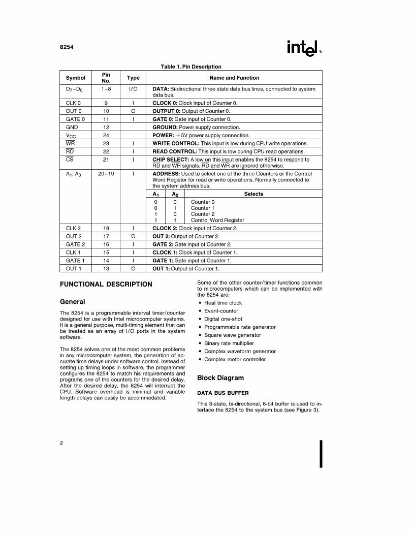
Table 1. Pin Description
SymbolPin
Type Name and FunctionNo.
D7–D0 1–8 I/O DATA: Bi-directional three state data bus lines, connected to systemdata bus.
CLK 0 9 I CLOCK 0: Clock input of Counter 0.
OUT 0 10 O OUTPUT 0: Output of Counter 0.
GATE 0 11 I GATE 0: Gate input of Counter 0.
GND 12 GROUND: Power supply connection.
VCC 24 POWER: a5V power supply connection.
WR 23 I WRITE CONTROL: This input is low during CPU write operations.
RD 22 I READ CONTROL: This input is low during CPU read operations.
CS 21 I CHIP SELECT: A low on this input enables the 8254 to respond toRD and WR signals. RD and WR are ignored otherwise.
A1, A0 20–19 I ADDRESS: Used to select one of the three Counters or the ControlWord Register for read or write operations. Normally connected tothe system address bus.
A1 A0 Selects
0 0 Counter 00 1 Counter 11 0 Counter 21 1 Control Word Register
CLK 2 18 I CLOCK 2: Clock input of Counter 2.
OUT 2 17 O OUT 2: Output of Counter 2.
GATE 2 16 I GATE 2: Gate input of Counter 2.
CLK 1 15 I CLOCK 1: Clock input of Counter 1.
GATE 1 14 I GATE 1: Gate input of Counter 1.
OUT 1 13 O OUT 1: Output of Counter 1.
FUNCTIONAL DESCRIPTION
General
The 8254 is a programmable interval timer/counterdesigned for use with Intel microcomputer systems.It is a general purpose, multi-timing element that canbe treated as an array of I/O ports in the systemsoftware.
The 8254 solves one of the most common problemsin any microcomputer system, the generation of ac-curate time delays under software control. Instead ofsetting up timing loops in software, the programmerconfigures the 8254 to match his requirements andprograms one of the counters for the desired delay.After the desired delay, the 8254 will interrupt theCPU. Software overhead is minimal and variablelength delays can easily be accommodated.
Some of the other counter/timer functions commonto microcomputers which can be implemented withthe 8254 are:
# Real time clock
# Event-counter
# Digital one-shot
# Programmable rate generator
# Square wave generator
# Binary rate multiplier
# Complex waveform generator
# Complex motor controller
Block Diagram
DATA BUS BUFFER
This 3-state, bi-directional, 8-bit buffer is used to in-terface the 8254 to the system bus (see Figure 3).
2

8254
231164–3
Figure 3. Block Diagram Showing Data Bus Buffer and Read/Write Logic Functions
READ/WRITE LOGIC
The Read/Write Logic accepts inputs from the sys-tem bus and generates control signals for the otherfunctional blocks of the 8254. A1 and A0 select oneof the three counters or the Control Word Registerto be read from/written into. A ‘‘low’’ on the RD in-put tells the 8254 that the CPU is reading one of thecounters. A ‘‘low’’ on the WR input tells the 8254that the CPU is writing either a Control Word or aninitial count. Both RD and WR are qualified by CS;RD and WR are ignored unless the 8254 has beenselected by holding CS low.
CONTROL WORD REGISTER
The Control Word Register (see Figure 4) is selectedby the Read/Write Logic when A1,A0 e 11. If theCPU then does a write operation to the 8254, thedata is stored in the Control Word Register and isinterpreted as a Control Word used to define theoperation of the Counters.
The Control Word Register can only be written to;status information is available with the Read-BackCommand.
COUNTER 0, COUNTER 1, COUNTER 2
These three functional blocks are identical in opera-tion, so only a single Counter will be described. Theinternal block diagram of a single counter is shownin Figure 5.
The Counters are fully independent. Each Countermay operate in a different Mode.
The Control Word Register is shown in the figure; itis not part of the Counter itself, but its contents de-termine how the Counter operates.
The status register, shown in Figure 5, whenlatched, contains the current contents of the ControlWord Register and status of the output and nullcount flag. (See detailed explanation of the Read-Back command.)
The actual counter is labelled CE (for ‘‘Counting Ele-ment’’). It is a 16-bit presettable synchronous downcounter.
OLM and OLL are two 8-bit latches. OL stands for‘‘Output Latch’’; the subscripts M and L stand for‘‘Most significant byte’’ and ‘‘Least significant byte’’
3

8254
231164–4
Figure 4. Block Diagram Showing Control Word Register and Counter Functions
231164–5
Figure 5. Internal Block Diagram of a Counter
4

8254
respectively. Both are normally referred to as oneunit and called just OL. These latches normally ‘‘fol-low’’ the CE, but if a suitable Counter Latch Com-mand is sent to the 8254, the latches ‘‘latch’’ thepresent count until read by the CPU and then returnto ‘‘following’’ the CE. One latch at a time is enabledby the counter’s Control Logic to drive the internalbus. This is how the 16-bit Counter communicatesover the 8-bit internal bus. Note that the CE itselfcannot be read; whenever you read the count, it isthe OL that is being read.
Similarly, there are two 8-bit registers called CRMand CRL (for ‘‘Count Register’’). Both are normallyreferred to as one unit and called just CR. When anew count is written to the Counter, the count isstored in the CR and later transferred to the CE. TheControl Logic allows one register at a time to beloaded from the internal bus. Both bytes are trans-ferred to the CE simultaneously. CRM and CRL arecleared when the Counter is programmed. In thisway, if the Counter has been programmed for onebyte counts (either most significant byte only or leastsignificant byte only) the other byte will be zero.Note that the CE cannot be written into; whenever acount is written, it is written into the CR.
The Control Logic is also shown in the diagram.CLK n, GATE n, and OUT n are all connected to theoutside world through the Control Logic.
8254 SYSTEM INTERFACE
The 8254 is a component of the Intel MicrocomputerSystems and interfaces in the same manner as all
other peripherals of the family. It is treated by thesystem’s software as an array of peripheral I/Oports; three are counters and the fourth is a controlregister for MODE programming.
Basically, the select inputs A0,A1 connect to the A0,A1 address bus signals of the CPU. The CS can bederived directly from the address bus using a linearselect method. Or it can be connected to the outputof a decoder, such as an Intel 8205 for larger sys-tems.
OPERATIONAL DESCRIPTION
General
After power-up, the state of the 8254 is undefined.The Mode, count value, and output of all Countersare undefined.
How each Counter operates is determined when it isprogrammed. Each Counter must be programmedbefore it can be used. Unused counters need not beprogrammed.
Programming the 8254
Counters are programmed by writing a Control Wordand then an initial count.
The Control Words are written into the Control WordRegister, which is selected when A1,A0 e 11. TheControl Word itself specifies which Counter is beingprogrammed.
231164–6
Figure 6. 8254 System Interface
5

8254
Control Word FormatA1,A0 e 11 CS e 0 RD e 1 WR e 0
D7 D6 D5 D4 D3 D2 D1 D0
SC1 SC0 RW1 RW0 M2 M1 M0 BCD
SCÐSelect Counter
SC1 SC0
0 0 Select Counter 0
0 1 Select Counter 1
1 0 Select Counter 2
1 1 Read-Back Command
(see Read Operations)
RWÐRead/Write
RW1 RW0
0 0 Counter Latch Command (see Read
Operations)
0 1 Read/Write least significant byte only
1 0 Read/Write most significant byte only
1 1 Read/Write least significant byte first,
then most significant byte
MÐMode
M2 M1 M0
0 0 0 Mode 0
0 0 1 Mode 1
X 1 0 Mode 2
X 1 1 Mode 3
1 0 0 Mode 4
1 0 1 Mode 5
BCD
0 Binary Counter 16-bits
1 Binary Coded Decimal (BCD) Counter
(4 Decades)
NOTE:Don’t care bits (X) should be 0 to insure compatibility with future Intel products.
Figure 7. Control Word Format
By contrast, initial counts are written into the Coun-ters, not the Control Word Register. The A1,A0 in-puts are used to select the Counter to be writteninto. The format of the initial count is determined bythe Control Word used.
Write Operations
The programming procedure for the 8254 is veryflexible. Only two conventions need to be remem-bered:
1) For each Counter, the Control Word must be writ-ten before the initial count is written.
2) The initial count must follow the count formatspecified in the Control Word (least significantbyte only, most significant byte only, or least sig-nificant byte and then most significant byte).
Since the Control Word Register and the threeCounters have separate addresses (selected by theA1,A0 inputs), and each Control Word specifies theCounter it applies to (SC0,SC1 bits), no special in-struction sequence is required. Any programmingsequence that follows the conventions in Figure 7 isacceptable.
A new initial count may be written to a Counter atany time without affecting the Counter’s pro-grammed Mode in any way. Counting will be affectedas described in the Mode definitions. The new countmust follow the programmed count format.
If a Counter is programmed to read/write two-bytecounts, the following precaution applies: A programmust not transfer control between writing the firstand second byte to another routine which also writesinto that same Counter. Otherwise, the Counter willbe loaded with an incorrect count.
6

8254
A1 A0
Control WordÐCounter 0 1 1
LSB of countÐCounter 0 0 0
MSB of countÐCounter 0 0 0
Control WordÐCounter 1 1 1
LSB of countÐCounter 1 0 1
MSB of countÐCounter 1 0 1
Control WordÐCounter 2 1 1
LSB of countÐCounter 2 1 0
MSB of countÐCounter 2 1 0
A1 A0
Control WordÐCounter 0 1 1
Control WordÐCounter 1 1 1
Control WordÐCounter 2 1 1
LSB of countÐCounter 2 1 0
LSB of countÐCounter 1 0 1
LSB of countÐCounter 0 0 0
MSB of countÐCounter 0 0 0
MSB of countÐCounter 1 0 1
MSB of countÐCounter 2 1 0
A1 A0
Control WordÐCounter 2 1 1
Control WordÐCounter 1 1 1
Control WordÐCounter 0 1 1
LSB of countÐCounter 2 1 0
MSB of countÐCounter 2 1 0
LSB of countÐCounter 1 0 1
MSB of countÐCounter 1 0 1
LSB of countÐCounter 0 0 0
MSB of countÐCounter 0 0 0
A1 A0
Control WordÐCounter 1 1 1
Control WordÐCounter 0 1 1
LSB of countÐCounter 1 0 1
Control WordÐCounter 2 1 1
LSB of countÐCounter 0 0 0
MSB of countÐCounter 1 0 1
LSB of countÐCounter 2 1 0
MSB of countÐCounter 0 0 0
MSB of countÐCounter 2 1 0
NOTE:In all four examples, all Counters are programmed to read/write two-byte counts. These are only four of many possibleprogramming sequences.
Figure 8. A Few Possible Programming Sequences
Read Operations
It is often desirable to read the value of a Counterwithout disturbing the count in progress. This is easi-ly done in the 8254.
There are three possible methods for reading thecounters: a simple read operation, the CounterLatch Command, and the Read-Back Command.Each is explained below. The first method is to per-form a simple read operation. To read the Counter,which is selected with the A1, A0 inputs, the CLKinput of the selected Counter must be inhibited byusing either the GATE input or external logic. Other-wise, the count may be in the process of changingwhen it is read, giving an undefined result.
COUNTER LATCH COMMAND
The second method uses the ‘‘Counter Latch Com-mand’’. Like a Control Word, this command is writtento the Control Word Register, which is selectedwhen A1,A0 e 11. Also like a Control Word, theSC0, SC1 bits select one of the three Counters, buttwo other bits, D5 and D4, distinguish this commandfrom a Control Word.
A1,A0 e 11; CS e 0; RD e 1; WR e 0
D7 D6 D5 D4 D3 D2 D1 D0
SC1 SC0 0 0 X X X X
SC1,SC0Ðspecify counter to be latched
SC1 SC0 Counter
0 0 0
0 1 1
1 0 2
1 1 Read-Back Command
D5,D4Ð00 designates Counter Latch Command
XÐdon’t care
NOTE:Don’t care bits (X) should be 0 to insure compatibilitywith future Intel products.
Figure 9. Counter Latching Command Format
7

8254
The selected Counter’s output latch (OL) latches thecount at the time the Counter Latch Command isreceived. This count is held in the latch until it is readby the CPU (or until the Counter is reprogrammed).The count is then unlatched automatically and theOL returns to ‘‘following’’ the counting element (CE).This allows reading the contents of the Counters‘‘on the fly’’ without affecting counting in progress.Multiple Counter Latch Commands may be used tolatch more than one Counter. Each latched Coun-ter’s OL holds its count until it is read. Counter LatchCommands do not affect the programmed Mode ofthe Counter in any way.
If a Counter is latched and then, some time later,latched again before the count is read, the secondCounter Latch Command is ignored. The count readwill be the count at the time the first Counter LatchCommand was issued.
With either method, the count must be read accord-ing to the programmed format; specifically, if theCounter is programmed for two byte counts, twobytes must be read. The two bytes do not have to beread one right after the other; read or write or pro-gramming operations of other Counters may be in-serted between them.
Another feature of the 8254 is that reads and writesof the same Counter may be interleaved; for exam-ple, if the Counter is programmed for two bytecounts, the following sequence is valid.
1) Read least significant byte.
2) Write new least significant byte.
3) Read most significant byte.
4) Write new most significant byte.
If a Counter is programmed to read/write two-bytecounts, the following precaution applies: A programmust not transfer control between reading the firstand second byte to another routine which also readsfrom that same Counter. Otherwise, an incorrectcount will be read.
READ-BACK COMMAND
The third method uses the Read-Back Command.This command allows the user to check the countvalue, programmed Mode, and current states of theOUT pin and Null Count flag of the selected coun-ter(s).
The command is written into the Control Word Reg-ister and has the format shown in Figure 10. Thecommand applies to the counters selected by set-ting their corresponding bits D3, D2, D1 e 1.
A0, A1 e 11 CS e 0 RD e 1 WR e 0
D7 D6 D5 D4 D3 D2 D1 D0
1 1 COUNT STATUS CNT 2 CNT 1 CNT 0 0
D5: 0 e Latch count of selected counter(s)D4: 0 e Latch status of selected counters(s)D3: 1 e Select Counter 2D2: 1 e Select Counter 1D1: 1 e Select Counter 0D0: Reserved for future expansion; Must be 0
Figure 10. Read-Back Command Format
The read-back command may be used to latch multi-ple counter output latches (OL) by setting theCOUNT bit D5 e 0 and selecting the desired coun-ter(s). This single command is functionally equiva-lent to several counter latch commands, one foreach counter latched. Each counter’s latched countis held until it is read (or the counter is repro-grammed). The counter is automatically unlatchedwhen read, but other counters remain latched untilthey are read. If multiple count read-back commandsare issued to the same counter without reading thecount, all but the first are ignored; i.e., the countwhich will be read is the count at the time the firstread-back command was issued.
The read-back command may also be used to latchstatus information of selected counter(s) by settingSTATUS bit D4 e 0. Status must be latched to beread; status of a counter is accessed by a read fromthat counter.
The counter status format is shown in Figure 11. BitsD5 through D0 contain the counter’s programmedMode exactly as written in the last Mode ControlWord. OUTPUT bit D7 contains the current state ofthe OUT pin. This allows the user to monitor thecounter’s output via software, possibly eliminatingsome hardware from a system.
D7 D6 D5 D4 D3 D2 D1 D0
OutputNull
RW1 RW0 M2 M1 M0 BCDCount
D7 1 e OUT Pin is 10 e OUT Pin is 0
D6 1 e Null Count0 e Count available for reading
D5–D0 Counter programmed mode (see Figure7)
Figure 11. Status Byte
8

8254
NULL COUNT bit D6 indicates when the last countwritten to the counter register (CR) has been loadedinto the counting element (CE). The exact time thishappens depends on the Mode of the counter and isdescribed in the Mode Definitions, but until the countis loaded into the counting element (CE), it can’t beread from the counter. If the count is latched or readbefore this time, the count value will not reflect thenew count just written. The operation of Null Countis shown in Figure 12.
This Action Causes
A. Write to the control word register;(1) Null Count e 1
B. Write to the count register (CR);(2) Null Count e 1
C. New Count is loaded into Null Count e 0
CE (CRxCE);
NOTE:1. Only the counter specified by the control word willhave its Null Count set to 1. Null count bits of othercounters are unaffected.2. If the counter is programmed for two-byte counts(least significant byte then most significant byte) NullCount goes to 1 when the second byte is written.
Figure 12. Null Count Operation
If multiple status latch operations of the counter(s)are performed without reading the status, all but thefirst are ignored; i.e., the status that will be read isthe status of the counter at the time the first statusread-back command was issued.
Both count and status of the selected counter(s)may be latched simultaneously by setting both
COUNT and STATUS bits D5,D4 e 0. This is func-tionally the same as issuing two separate read-backcommands at once, and the above discussions ap-ply here also. Specifically, if multiple count and/orstatus read-back commands are issued to the samecounter(s) without any intervening reads, all but thefirst are ignored. This is illustrated in Figure 13.
If both count and status of a counter are latched, thefirst read operation of that counter will return latchedstatus, regardless of which was latched first. Thenext one or two reads (depending on whether thecounter is programmed for one or two type counts)return latched count. Subsequent reads return un-latched count.
CS RD WR A1 A0
0 1 0 0 0 Write into Counter 0
0 1 0 0 1 Write into Counter 1
0 1 0 1 0 Write into Counter 2
0 1 0 1 1 Write Control Word
0 0 1 0 0 Read from Counter 0
0 0 1 0 1 Read from Counter 1
0 0 1 1 0 Read from Counter 2
0 0 1 1 1 No-Operation (3-State)
1 X X X X No-Operation (3-State)
0 1 1 X X No-Operation (3-State)
Figure 14. Read/Write Operations Summary
CommandDescription Result
D7 D6 D5 D4 D3 D2 D1 D0
1 1 0 0 0 0 1 0 Read back count and status of Count and status latched
Counter 0 for Counter 0
1 1 1 0 0 1 0 0 Read back status of Counter 1 Status latched for Counter 1
1 1 1 0 1 1 0 0 Read back status of Counters 2, 1 Status latched for Counter
2, but not Counter 1
1 1 0 1 1 0 0 0 Read back count of Counter 2 Count latched for Counter 2
1 1 0 0 0 1 0 0 Read back count and status of Count latched for Counter 1,
Counter 1 but not status
1 1 1 0 0 0 1 0 Read back status of Counter 1 Command ignored, status
already latched for Counter 1
Figure 13. Read-Back Command Example
9

8254
Mode Definitions
The following are defined for use in describing theoperation of the 8254.
CLK Pulse: a rising edge, then a falling edge, inthat order, of a Counter’s CLK in-put.
Trigger: a rising edge of a Counter’s GATEinput.
Counter loading: the transfer of a count from the CRto the CE (refer to the ‘‘FunctionalDescription’’)
MODE 0: INTERRUPT ON TERMINAL COUNT
Mode 0 is typically used for event counting. After theControl Word is written, OUT is initially low, and willremain low until the Counter reaches zero. OUT thengoes high and remains high until a new count or anew Mode 0 Control Word is written into the Coun-ter.
GATE e 1 enables counting; GATE e 0 disablescounting. GATE has no effect on OUT.
After the Control Word and initial count are written toa Counter, the initial count will be loaded on the nextCLK pulse. This CLK pulse does not decrement thecount, so for an initial count of N, OUT does not gohigh until N a 1 CLK pulses after the initial count iswritten.
If a new count is written to the Counter, it will beloaded on the next CLK pulse and counting will con-tinue from the new count. If a two-byte count is writ-ten, the following happens:
1) Writing the first byte disables counting. OUT is setlow immediately (no clock pulse required)
2) Writing the second byte allows the new count tobe loaded on the next CLK pulse.
This allows the counting sequence to be synchroniz-ed by software. Again, OUT does not go high untilNa1 CLK pulses after the new count of N is written.
If an initial count is written while GATE e 0, it willstill be loaded on the next CLK pulse. When GATEgoes high, OUT will go high N CLK pulses later; noCLK pulse is needed to load the Counter as this hasalready been done.
MODE 1: HARDWARE RETRIGGERABLEONE-SHOT
OUT will be initially high. OUT will go low on the CLKpulse following a trigger to begin the one-shot pulse,and will remain low until the Counter reaches zero.
OUT will then go high and remain high until the CLKpulse after the next trigger.
After writing the Control Word and initial count, theCounter is armed. A trigger results in loading theCounter and setting OUT low on the next CLK pulse,thus starting the one-shot pulse. An initial count of Nwill result in a one-shot pulse N CLK cycles in dura-tion. The one-shot is retriggerable, hence OUT willremain low for N CLK pulses after any trigger. Theone-shot pulse can be repeated without rewriting thesame count into the counter. GATE has no effect onOUT.
If a new count is written to the Counter during a one-shot pulse, the current one-shot is not affected un-less the counter is retriggered. In that case, theCounter is loaded with the new count and the one-shot pulse continues until the new count expires.
MODE 2: RATE GENERATOR
This Mode functions like a divide-by-N counter. It istypically used to generate a Real Time Clock inter-rupt. OUT will initially be high. When the initial counthas decremented to 1, OUT goes low for one CLKpulse. OUT then goes high again, the Counter re-loads the initial count and the process is repeated.Mode 2 is periodic; the same sequence is repeatedindefinitely. For an initial count of N, the sequencerepeats every N CLK cycles.
GATE e 1 enables counting; GATE e 0 disablescounting. If GATE goes low during an output pulse,OUT is set high immediately. A trigger reloads theCounter with the initial count on the next CLK pulse;OUT goes low N CLK pulses after the trigger. Thusthe GATE input can be used to synchronize theCounter.
After writing a Control Word and initial count, theCounter will be loaded on the next CLK pulse. OUTgoes low N CLK Pulses after the initial count is writ-ten. This allows the Counter to be synchronized bysoftware also.
Writing a new count while counting does not affectthe current counting sequence. If a trigger is re-ceived after writing a new count but before the endof the current period, the Counter will be loaded withthe new count on the next CLK pulse and countingwill continue from the new count. Otherwise, thenew count will be loaded at the end of the currentcounting cycle. In mode 2, a COUNT of 1 is illegal.
MODE 3: SQUARE WAVE MODE
Mode 3 is typically used for Baud rate generation.Mode 3 is similar to Mode 2 except for the duty cycleof OUT. OUT will initially be high. When half the
10

8254
231164–7
NOTE:The following conventions apply to all mode timing diagrams:1. Counters are programmed for binary (not BCD) counting and for reading/writing least significant byte (LSB) only.2. The counter is always selected (CS always low).3. CW stands for ‘‘Control Word’’; CW e 10 means a control word of 10 HEX is written to the counter.4. LSB stands for ‘‘Least Significant Byte’’ of count.5. Numbers below diagrams are count values. The lower number is the least significant byte. The upper number is themost significant byte. Since the counter is programmed to read/write LSB only, the most significant byte cannot be read.
N stands for an undefined count.Vertical lines show transitions between count values.
Figure 15. Mode 0
11

8254
231164–8
Figure 16. Mode 1
initial count has expired, OUT goes low for the re-mainder of the count. Mode 3 is periodic; the se-quence above is repeated indefinitely. An initialcount of N results in a square wave with a period ofN CLK cycles.
GATE e 1 enables counting; GATE e 0 disablescounting. If GATE goes low while OUT is low, OUT isset high immediately; no CLK pulse is required. Atrigger reloads the Counter with the initial count onthe next CLK pulse. Thus the GATE input can beused to synchronize the Counter.
After writing a Control Word and initial count, theCounter will be loaded on the next CLK pulse. Thisallows the Counter to be synchronized by softwarealso.
Writing a new count while counting does not affectthe current counting sequence. If a trigger is re-ceived after writing a new count but before the endof the current half-cycle of the square wave, theCounter will be loaded with the new count on thenext CLK pulse and counting will continue from the
12

8254
231164–9
NOTE:A GATE transition should not occur one clock prior to terminal count.
Figure 17. Mode 2
new count. Otherwise, the new count will be loadedat the end of the current half-cycle.
Mode 3 is implemented as follows:
Even counts: OUT is initially high. The initial count isloaded on one CLK pulse and then is decrementedby two on succeeding CLK pulses. When the countexpires OUT changes value and the Counter is re-loaded with the initial count. The above process isrepeated indefinitely.
Odd counts: OUT is initially high. The initial countminus one (an even number) is loaded on one CLKpulse and then is decremented by two on succeed-ing CLK pulses. One CLK pulse after the count ex-pires, OUT goes low and the Counter is reloadedwith the initial count minus one. Succeeding CLKpulses decrement the count by two. When the countexpires, OUT goes high again and the Counter isreloaded with the initial count minus one. The aboveprocess is repeated indefinitely. So for odd counts,OUT will be high for (N a 1)/2 counts and low for(N b 1)/2 counts.
13

8254
231164–10
NOTE:A GATE transition should not occur one clock prior to terminal count.
Figure 18. Mode 3
14

8254
MODE 4: SOFTWARE TRIGGERED STROBE
OUT will be initially high. When the initial count ex-pires, OUT will go low for one CLK pulse and thengo high again. The counting sequence is ‘‘triggered’’by writing the initial count.
GATE e 1 enables counting; GATE e 0 disablescounting. GATE has no effect on OUT.
After writing a Control Word and initial count, theCounter will be loaded on the next CLK pulse. ThisCLK pulse does not decrement the count, so for an
initial count of N, OUT does not strobe low until N a
1 CLK pulses after the initial count is written.
If a new count is written during counting, it will beloaded on the next CLK pulse and counting will con-tinue from the new count. If a two-byte count is writ-ten, the following happens:
1) Writing the first byte has no effect on counting.
2) Writing the second byte allows the new count tobe loaded on the next CLK pulse.
This allows the sequence to be ‘‘retriggered’’ bysoftware. OUT strobes low N a 1 CLK pulses afterthe new count of N is written.
231164–11
Figure 19. Mode 4
15

8254
MODE 5: HARDWARE TRIGGERED STROBE(RETRIGGERABLE)
OUT will initially be high. Counting is triggered by arising edge of GATE. When the initial count has ex-pired, OUT will go low for one CLK pulse and thengo high again.
After writing the Control Word and initial count, thecounter will not be loaded until the CLK pulse after atrigger. This CLK pulse does not decrement thecount, so for an initial count of N, OUT does notstrobe low until N a 1 CLK pulses after a trigger.
A trigger results in the Counter being loaded with theinitial count on the next CLK pulse. The countingsequence is retriggerable. OUT will not strobe lowfor N a 1 CLK pulses after any trigger. GATE hasno effect on OUT.
If a new count is written during counting, the currentcounting sequence will not be affected. If a triggeroccurs after the new count is written but before thecurrent count expires, the Counter will be loadedwith the new count on the next CLK pulse andcounting will continue from there.
231164–12
Figure 20. Mode 5
16

8254
Signal Low
Status Or Going Rising High
Modes Low
0 Disables Ð Ð Enables
Counting Counting
1 Ð Ð 1) Initiates Ð Ð
Counting
2) Resets Output
after Next
Clock
2 1) Disables
Counting Initiates Enables
2) Sets Output Counting Counting
Immediately
High
3 1) Disables
Counting Initiates Enables
2) Sets Output Counting Counting
Immediately
High
4 Disables Ð Ð Enables
Counting Counting
5 Ð Ð Initiates Ð Ð
Counting
Figure 21. Gate Pin Operations Summary
ModeMin Max
Count Count
0 1 0
1 1 0
2 2 0
3 2 0
4 1 0
5 1 0
NOTE:0 is equivalent to 216 for binary counting and 104 forBCD counting.
Figure 22. Minimum and Maximum Initial Counts
Operation Common to All Modes
PROGRAMMING
When a Control Word is written to a Counter, allControl Logic is immediately reset and OUT goes toa known initial state; no CLK pulses are required forthis.
GATE
The GATE input is always sampled on the risingedge of CLK. In Modes 0, 2, 3, and 4 the GATE inputis level sensitive, and the logic level is sampled onthe rising edge of CLK. In Modes 1, 2, 3, and 5 theGATE input is rising-edge sensitive. In these Modes,a rising edge of GATE (trigger) sets an edge-sensi-tive flip-flop in the Counter. This flip-flop is then sam-pled on the next rising edge of CLK; the flip-flop isreset immediately after it is sampled. In this way, atrigger will be detected no matter when it occursÐahigh logic level does not have to be maintained untilthe next rising edge of CLK. Note that in Modes 2and 3, the GATE input is both edge- and level-sensi-tive. In Modes 2 and 3, if a CLK source other thanthe system clock is used, GATE should be pulsedimmediately following WR of a new count value.
COUNTER
New counts are loaded and Counters are decre-mented on the falling edge of CLK.
The largest possible initial count is 0; this is equiva-lent to 216 for binary counting and 104 for BCDcounting.
The Counter does not stop when it reaches zero. InModes 0, 1, 4, and 5 the Counter ‘‘wraps around’’ tothe highest count, either FFFF hex for binary count-ing or 9999 for BCD counting, and continues count-ing. Modes 2 and 3 are periodic; the Counter reloadsitself with the initial count and continues countingfrom there.
17

8254
ABSOLUTE MAXIMUM RATINGS*
Ambient Temperature Under Bias ÀÀÀÀÀÀ0§C to 70§CStorage Temperature ÀÀÀÀÀÀÀÀÀÀb65§C to a150§CVoltage on Any Pin with
Respect to GroundÀÀÀÀÀÀÀÀÀÀÀÀÀÀb0.5V to a7V
Power Dissipation ÀÀÀÀÀÀÀÀÀÀÀÀÀÀÀÀÀÀÀÀÀÀÀÀÀÀÀ1W
NOTICE: This is a production data sheet. The specifi-cations are subject to change without notice.
*WARNING: Stressing the device beyond the ‘‘AbsoluteMaximum Ratings’’ may cause permanent damage.These are stress ratings only. Operation beyond the‘‘Operating Conditions’’ is not recommended and ex-tended exposure beyond the ‘‘Operating Conditions’’may affect device reliability.
D.C. CHARACTERISTICS TA e 0§C to 70§C, VCC e 5V g10%
Symbol Parameter Min Max Units Test Conditions
VIL Input Low Voltage b0.5 0.8 V
VIH Input High Voltage 2.0 VCC a0.5V V
VOL Output Low Voltage 0.45 V IOL e 2.0 mA
VOH Output High Voltage 2.4 V IOH e b400 mA
IIL Input Load Current g10 mA VIN e VCC to 0V
IOFL Output Float Leakage g10 mA VOUT e VCC to 0.45V
ICC VCC Supply Current 170 mA
CIN Input Capacitance 10 pF fc e 1 MHz
CI/0 I/O Capacitance 20 pF Unmeasured pins
returned to VSS(4)
A.C. CHARACTERISTICS TA e 0§C to 70§C, VCC e 5V g10%, GND e 0V
Bus Parameters(1)
READ CYCLE
Symbol Parameter8254 8254-2
UnitMin Max Min Max
tAR Address Stable Before RDv 45 30 ns
tSR CS Stable Before RDv 0 0 ns
tRA Address Hold Time After RDu 0 0 ns
tRR RD Pulse Width 150 95 ns
tRD Data Delay from RDv 120 85 ns
tAD Data Delay from Address 220 185 ns
tDF RDu to Data Floating 5 90 5 65 ns
tRV Command Recovery Time 200 165 ns
NOTE:1. AC timings measured at VOH e 2.0V, VOL e 0.8V.
18

8254
A.C. CHARACTERISTICS TA e 0§C to 70§C, VCC e 5V g10%, GND e 0V (Continued)
WRITE CYCLE
Symbol Parameter8254 8254-2
UnitMin Max Min Max
tAW Address Stable Before WRv 0 0 ns
tSW CS Stable Before WRv 0 0 ns
tWA Address Hold Time After WRv 0 0 ns
tWW WR Pulse Width 150 95 ns
tDW Data Setup Time Before WRu 120 95 ns
tWD Data Hold Time After WRu 0 0 ns
tRV Command Recovery Time 200 165 ns
CLOCK AND GATE
Symbol Parameter8254 8254-2
UnitMin Max Min Max
tCLK Clock Period 125 DC 100 DC ns
tPWH High Pulse Width 60(3) 30(3) ns
tPWL Low Pulse Width 60(3) 50(3) ns
tR Clock Rise Time 25 25 ns
tF Clock Fall Time 25 25 ns
tGW Gate Width High 50 50 ns
tGL Gate Width Low 50 50 ns
tGS Gate Setup Time to CLKu 50 40 ns
tGH Gate Setup Time After CLKu 50(2) 50(2) ns
tOD Output Delay from CLKv 150 100 ns
tODG Output Delay from Gatev 120 100 ns
tWC CLK Delay for Loadingv 0 55 0 55 ns
tWG Gate Delay for Sampling b5 50 b5 40 ns
tWO OUT Delay from Mode Write 260 240 ns
tCL CLK Set Up for Count Latch b40 45 b40 40 ns
NOTES:2. In Modes 1 and 5 triggers are sampled on each rising clock edge. A second trigger within 120 ns (70 ns for the 8254-2) ofthe rising clock edge may not be detected.3. Low-going glitches that violate tPWH, tPWL may cause errors requiring counter reprogramming.4. Sampled, not 100% tested. TA e 25§C.5. If CLK present at TWC min then Count equals Na2 CLK pulses, TWC max equals Count Na1 CLK pulse. TWC min toTWC max, count will be either Na1 or Na2 CLK pulses.6. In Modes 1 and 5, if GATE is present when writing a new Count value, at TWG min Counter will not be triggered, at TWGmax Counter will be triggered.7. If CLK present when writing a Counter Latch or ReadBack Command, at TCL min CLK will be reflected in count valuelatched, at TCL max CLK will not be reflected in the count value latched.
19

8254
WAVEFORMS
WRITE
231164–13
READ
231164–14
20

8254
WAVEFORMS (Continued)
RECOVERY
231164–15
CLOCK AND GATE
231164–16
*Last byte of count being written.
A.C. TESTING INPUT, OUTPUT WAVEFORM
231164–17
A.C. Testing: Inputs are driven at 2.4V for a Logic ‘‘1’’ and 0.45Vfor a Logic ‘‘0.’’ Timing measurements are made at 2.0V for aLogic ‘‘1’’ and 0.8V for a Logic ‘‘0’’.
A.C. TESTING LOAD CIRCUIT
231164–18CL e 150 pFCL Includes Jig Capacitance
REVISION SUMMARY
The following list represents the key differences be-tween Rev. 004 and Rev. 005 of the 8254 DataSheet.
1. References to and specifications for the 5 MHz8254-5 are removed. Only the 8 MHz 8254 andthe 10 MHz 8254-2 remain in production.
21

THIS PAGE IN TEN TION ALLY LEFT BLANK

6 APPENDIX D
8259A Datasheet Reprint

THIS PAGE IN TEN TION ALLY LEFT BLANK

December 1988 Order Number: 231468-003
8259APROGRAMMABLE INTERRUPT CONTROLLER
(8259A/8259A-2)
Y 8086, 8088 Compatible
Y MCS-80, MCS-85 Compatible
Y Eight-Level Priority Controller
Y Expandable to 64 Levels
Y Programmable Interrupt Modes
Y Individual Request Mask Capability
Y Single a5V Supply (No Clocks)
Y Available in 28-Pin DIP and 28-LeadPLCC Package(See Packaging Spec., Order Ý231369)
Y Available in EXPRESSÐ Standard Temperature RangeÐ Extended Temperature Range
The Intel 8259A Programmable Interrupt Controller handles up to eight vectored priority interrupts for the CPU.It is cascadable for up to 64 vectored priority interrupts without additional circuitry. It is packaged in a 28-pinDIP, uses NMOS technology and requires a single a5V supply. Circuitry is static, requiring no clock input.
The 8259A is designed to minimize the software and real time overhead in handling multi-level priority inter-rupts. It has several modes, permitting optimization for a variety of system requirements.
The 8259A is fully upward compatible with the Intel 8259. Software originally written for the 8259 will operatethe 8259A in all 8259 equivalent modes (MCS-80/85, Non-Buffered, Edge Triggered).
231468–1
Figure 1. Block Diagram
DIP
231468–2
PLCC
231468–31
Figure 2. Pin
Configurations

8259A
Table 1. Pin Description
Symbol Pin No. Type Name and Function
VCC 28 I SUPPLY: a5V Supply.
GND 14 I GROUND
CS 1 I CHIP SELECT: A low on this pin enables RD and WR communicationbetween the CPU and the 8259A. INTA functions are independent ofCS.
WR 2 I WRITE: A low on this pin when CS is low enables the 8259A to acceptcommand words from the CPU.
RD 3 I READ: A low on this pin when CS is low enables the 8259A to releasestatus onto the data bus for the CPU.
D7–D0 4–11 I/O BIDIRECTIONAL DATA BUS: Control, status and interrupt-vectorinformation is transferred via this bus.
CAS0–CAS2 12, 13, 15 I/O CASCADE LINES: The CAS lines form a private 8259A bus to controla multiple 8259A structure. These pins are outputs for a master 8259Aand inputs for a slave 8259A.
SP/EN 16 I/O SLAVE PROGRAM/ENABLE BUFFER: This is a dual function pin.When in the Buffered Mode it can be used as an output to controlbuffer transceivers (EN). When not in the buffered mode it is used asan input to designate a master (SP e 1) or slave (SP e 0).
INT 17 O INTERRUPT: This pin goes high whenever a valid interrupt request isasserted. It is used to interrupt the CPU, thus it is connected to theCPU’s interrupt pin.
IR0–IR7 18–25 I INTERRUPT REQUESTS: Asynchronous inputs. An interrupt requestis executed by raising an IR input (low to high), and holding it high untilit is acknowledged (Edge Triggered Mode), or just by a high level on anIR input (Level Triggered Mode).
INTA 26 I INTERRUPT ACKNOWLEDGE: This pin is used to enable 8259Ainterrupt-vector data onto the data bus by a sequence of interruptacknowledge pulses issued by the CPU.
A0 27 I AO ADDRESS LINE: This pin acts in conjunction with the CS, WR, andRD pins. It is used by the 8259A to decipher various Command Wordsthe CPU writes and status the CPU wishes to read. It is typicallyconnected to the CPU A0 address line (A1 for 8086, 8088).
2

8259A
FUNCTIONAL DESCRIPTION
Interrupts in Microcomputer Systems
Microcomputer system design requires that I.O de-vices such as keyboards, displays, sensors and oth-er components receive servicing in a an efficientmanner so that large amounts of the total systemtasks can be assumed by the microcomputer withlittle or no effect on throughput.
The most common method of servicing such devic-es is the Polled approach. This is where the proces-sor must test each device in sequence and in effect‘‘ask’’ each one if it needs servicing. It is easy to seethat a large portion of the main program is loopingthrough this continuous polling cycle and that such amethod would have a serious detrimental effect onsystem throughput, thus limiting the tasks that couldbe assumed by the microcomputer and reducing thecost effectiveness of using such devices.
A more desirable method would be one that wouldallow the microprocessor to be executing its mainprogram and only stop to service peripheral deviceswhen it is told to do so by the device itself. In effect,the method would provide an external asynchronousinput that would inform the processor that it shouldcomplete whatever instruction that is currently beingexecuted and fetch a new routine that will servicethe requesting device. Once this servicing is com-plete, however, the processor would resume exactlywhere it left off.
This method is called Interrupt . It is easy to see thatsystem throughput would drastically increase, andthus more tasks could be assumed by the micro-computer to further enhance its cost effectiveness.
The Programmable Interrupt Controller (PIC) func-tions as an overall manager in an Interrupt-Drivensystem environment. It accepts requests from theperipheral equipment, determines which of the in-coming requests is of the highest importance (priori-ty), ascertains whether the incoming request has ahigher priority value than the level currently beingserviced, and issues an interrupt to the CPU basedon this determination.
Each peripheral device or structure usually has aspecial program or ‘‘routine’’ that is associated withits specific functional or operational requirements;this is referred to as a ‘‘service routine’’. The PIC,after issuing an Interrupt to the CPU, must somehowinput information into the CPU that can ‘‘point’’ theProgram Counter to the service routine associatedwith the requesting device. This ‘‘pointer’’ is an ad-dress in a vectoring table and will often be referredto, in this document, as vectoring data.
231468–3
Figure 3a. Polled Method
231468–4
Figure 3b. Interrupt Method
3

8259A
The 8259A is a device specifically designed for usein real time, interrupt driven microcomputer systems.It manages eight levels or requests and has built-infeatures for expandability to other 8259A’s (up to 64levels). It is programmed by the system’s softwareas an I/O peripheral. A selection of priority modes isavailable to the programmer so that the manner inwhich the requests are processed by the 8259A canbe configured to match his system requirements.The priority modes can be changed or reconfigureddynamically at any time during the main program.This means that the complete interrupt structure canbe defined as required, based on the total systemenvironment.
INTERRUPT REQUEST REGISTER (IRR) ANDIN-SERVICE REGISTER (ISR)
The interrupts at the IR input lines are handled bytwo registers in cascade, the Interrupt Request Reg-ister (IRR) and the In-Service (ISR). The IRR is usedto store all the interrupt levels which are requestingservice; and the ISR is used to store all the interruptlevels which are being serviced.
PRIORITY RESOLVER
This logic block determines the priorites of the bitsset in the IRR. The highest priority is selected andstrobed into the corresponding bit of the ISR duringINTA pulse.
INTERRUPT MASK REGISTER (IMR)
The IMR stores the bits which mask the interruptlines to be masked. The IMR operates on the IRR.Masking of a higher priority input will not affect theinterrupt request lines of lower quality.
INT (INTERRUPT)
This output goes directly to the CPU interrupt input.The VOH level on this line is designed to be fullycompatible with the 8080A, 8085A and 8086 inputlevels.
INTA (INTERRUPT ACKNOWLEDGE)
INTA pulses will cause the 8259A to release vector-ing information onto the data bus. The format of thisdata depends on the system mode (mPM) of the8259A.
DATA BUS BUFFER
This 3-state, bidirectional 8-bit buffer is used to inter-face the 8259A to the system Data Bus. Controlwords and status information are transferredthrough the Data Bus Buffer.
READ/WRITE CONTROL LOGIC
The function of this block is to accept OUTput com-mands from the CPU. It contains the InitializationCommand Word (ICW) registers and OperationCommand Word (OCW) registers which store thevarious control formats for device operation. Thisfunction block also allows the status of the 8259A tobe transferred onto the Data Bus.
CS (CHIP SELECT)
A LOW on this input enables the 8259A. No readingor writing of the chip will occur unless the device isselected.
WR (WRITE)
A LOW on this input enables the CPU to write con-trol words (ICWs and OCWs) to the 8259A.
RD (READ)
A LOW on this input enables the 8259A to send thestatus of the Interrupt Request Register (IRR), InService Register (ISR), the Interrupt Mask Register(IMR), or the Interrupt level onto the Data Bus.
A0
This input signal is used in conjunction with WR andRD signals to write commands into the various com-mand registers, as well as reading the various statusregisters of the chip. This line can be tied directly toone of the address lines.
4

8259A
231468–5
Figure 4a. 8259A Block Diagram
5

8259A
231468–6
Figure 4b. 8259A Block Diagram
6

8259A
THE CASCADE BUFFER/COMPARATOR
This function block stores and compares the IDs ofall 8259A’s used in the system. The associatedthree I/O pins (CAS0-2) are outputs when the 8259Ais used as a master and are inputs when the 8259Ais used as a slave. As a master, the 8259A sendsthe ID of the interrupting slave device onto theCAS0–2 lines. The slave thus selected will send itspreprogrammed subroutine address onto the DataBus during the next one or two consecutive INTApulses. (See section ‘‘Cascading the 8259A’’.)
INTERRUPT SEQUENCE
The powerful features of the 8259A in a microcom-puter system are its programmability and the inter-rupt routine addressing capability. The latter allowsdirect or indirect jumping to the specific interrupt rou-tine requested without any polling of the interruptingdevices. The normal sequence of events during aninterrupt depends on the type of CPU being used.
The events occur as follows in an MCS-80/85 sys-tem:
1. One or more of the INTERRUPT REQUEST lines(IR7–0) are raised high, setting the correspond-ing IRR bit(s).
2. The 8259A evaluates these requests, and sendsan INT to the CPU, if appropriate.
3. The CPU acknowledges the INT and respondswith an INTA pulse.
4. Upon receiving an INTA from the CPU group, thehighest priority ISR bit is set, and the correspond-ing IRR bit is reset. The 8259A will also release aCALL instruction code (11001101) onto the 8-bitData Bus through its D7–0 pins.
5. This CALL instruction will initiate two more INTApulses to be sent to the 8259A from the CPUgroup.
6. These two INTA pulses allow the 8259A to re-lease its preprogrammed subroutine addressonto the Data Bus. The lower 8-bit address is re-
leased at the first INTA pulse and the higher 8-bitaddress is released at the second INTA pulse.
7. This completes the 3-byte CALL instruction re-leased by the 8259A. In the AEOI mode the ISRbit is reset at the end of the third INTA pulse.Otherwise, the ISR bit remains set until an appro-priate EOI command is issued at the end of theinterrupt sequence.
The events occuring in an 8086 system are thesame until step 4.
4. Upon receiving an INTA from the CPU group, thehighest priority ISR bit is set and the correspond-ing IRR bit is reset. The 8259A does not drive theData Bus during this cycle.
5. The 8086 will initiate a second INTA pulse. Dur-ing this pulse, the 8259A releases an 8-bit pointeronto the Data Bus where it is read by the CPU.
6. This completes the interrupt cycle. In the AEOImode the ISR bit is reset at the end of the sec-ond INTA pulse. Otherwise, the ISR bit remainsset until an appropriate EOI command is issuedat the end of the interrupt subroutine.
If no interrupt request is present at step 4 of eithersequence (i.e., the request was too short in duration)the 8259A will issue an interrupt level 7. Both thevectoring bytes and the CAS lines will look like aninterrupt level 7 was requested.
When the 8259A PIC receives an interrupt, INT be-comes active and an interrupt acknowledge cycle isstarted. If a higher priority interrupt occurs betweenthe two INTA pulses, the INT line goes inactive im-mediately after the second INTA pulse. After an un-specified amount of time the INT line is activatedagain to signify the higher priority interrupt waitingfor service. This inactive time is not specified andcan vary between parts. The designer should beaware of this consideration when designing a sys-tem which uses the 8259A. It is recommended thatproper asynchronous design techniques be fol-lowed.
7

8259A
231468–7
Figure 4c. 8259A Block Diagram
231468–8
Figure 5. 8259A Interface to
Standard System Bus
INTERRUPT SEQUENCE OUTPUTS
MCS-80, MCS-85
This sequence is timed by three INTA pulses. Duringthe first INTA pulse the CALL opcode is enabledonto the data bus.
Content of First Interrupt Vector Byte
D7 D6 D5 D4 D3 D2 D1 D0
CALL CODE 1 1 0 0 1 1 0 1
During the second INTA pulse the lower address ofthe appropriate service routine is enabled onto thedata bus. When Interval e 4 bits A5–A7 are pro-grammed, while A0–A4 are automatically inserted bythe 8259A. When Interval e 8 only A6 and A7 areprogrammed, while A0–A5 are automatically insert-ed.
8

8259A
Content of Second Interrupt Vector Byte
IR Interval e 4
D7 D6 D5 D4 D3 D2 D1 D0
7 A7 A6 A5 1 1 1 0 0
6 A7 A6 A5 1 1 0 0 0
5 A7 A6 A5 1 0 1 0 0
4 A7 A6 A5 1 0 0 0 0
3 A7 A6 A5 0 1 1 0 0
2 A7 A6 A5 0 1 0 0 0
1 A7 A6 A5 0 0 1 0 0
0 A7 A6 A5 0 0 0 0 0
IR Interval e 8
D7 D6 D5 D4 D3 D2 D1 D0
7 A7 A6 1 1 1 0 0 0
6 A7 A6 1 1 0 0 0 0
5 A7 A6 1 0 1 0 0 0
4 A7 A6 1 0 0 0 0 0
3 A7 A6 0 1 1 0 0 0
2 A7 A6 0 1 0 0 0 0
1 A7 A6 0 0 1 0 0 0
0 A7 A6 0 0 0 0 0 0
During the third INTA pulse the higher address of theappropriate service routine, which was programmedas byte 2 of the initialization sequence (A8–A15), isenabled onto the bus.
Content of Third Interrupt Vector Byte
D7 D6 D5 D4 D3 D2 D1 D0
A15 A14 A13 A12 A11 A10 A9 A8
8086, 8088
8086 mode is similar to MCS-80 mode except thatonly two Interrupt Acknowledge cycles are issued bythe processor and no CALL opcode is sent to theprocessor. The first interrupt acknowledge cycle issimilar to that of MCS-80, 85 systems in that the8259A uses it to internally freeze the state of theinterrupts for priority resolution and as a master itissues the interrupt code on the cascade lines at theend of the INTA pulse. On this first cycle it does notissue any data to the processor and leaves its databus buffers disabled. On the second interrupt ac-knowledge cycle in 8086 mode the master (or slaveif so programmed) will send a byte of data to theprocessor with the acknowledged interrupt code
composed as follows (note the state of the ADImode control is ignored and A5–A11 are unused in8086 mode):
Content of Interrupt Vector Byte
for 8086 System Mode
D7 D6 D5 D4 D3 D2 D1 D0
IR7 T7 T6 T5 T4 T3 1 1 1
IR6 T7 T6 T5 T4 T3 1 1 0
IR5 T7 T6 T5 T4 T3 1 0 1
IR4 T7 T6 T5 T4 T3 1 0 0
IR3 T7 T6 T5 T4 T3 0 1 1
IR2 T7 T6 T5 T4 T3 0 1 0
IR1 T7 T6 T5 T4 T3 0 0 1
IR0 T7 T6 T5 T4 T3 0 0 0
PROGRAMMING THE 8259A
The 8259A accepts two types of command wordsgenerated by the CPU:
1. Initialization Command Words (ICWs): Beforenormal operation can begin, each 8259A in thesystem must be brought to a starting pointÐby asequence of 2 to 4 bytes timed by WR pulses.
2. Operation Command Words (OCWs): These arethe command words which command the 8259Ato operate in various interrupt modes. Thesemodes are:
a. Fully nested mode
b. Rotating priority mode
c. Special mask mode
d. Polled mode
The OCWs can be written into the 8259A anytimeafter initialization.
INITIALIZATION COMMAND WORDS(ICWS)
General
Whenever a command is issued with A0 e 0 and D4e 1, this is interpreted as Initialization CommandWord 1 (ICW1). ICW1 starts the intiitalization se-quence during which the following automatically oc-cur.
a. The edge sense circuit is reset, which means thatfollowing initialization, an interrupt request (IR) in-put must make a low-to-high transistion to gener-ate an interrupt.
9

8259A
b. The Interrupt Mask Register is cleared.
c. IR7 input is assigned priority 7.
d. The slave mode address is set to 7.
e. Special Mask Mode is cleared and Status Read isset to IRR.
f. If IC4 e 0, then all functions selected in ICW4are set to zero. (Non-Buffered mode*, no Auto-EOI, MCS-80, 85 system).
*NOTE:Master/Slave in ICW4 is only used in the bufferedmode.
Initialization Command Words 1 and 2(ICW1, ICW2)
A5–A15: Page starting address of service routines .In an MCS 80/85 system, the 8 request levels willgenerate CALLs to 8 locations equally spaced inmemory. These can be programmed to be spaced atintervals of 4 or 8 memory locations, thus the 8 rou-tines will occupy a page of 32 or 64 bytes, respec-tively.
The address format is 2 bytes long (A0–A15). Whenthe routine interval is 4, A0–A4 are automatically in-serted by the 8259A, while A5–A15 are programmedexternally. When the routine interval is 8, A0–A5 areautomatically inserted by the 8259A, while A6–A15are programmed externally.
The 8-byte interval will maintain compatibility withcurrent software, while the 4-byte interval is best fora compact jump table.
In an 8086 system A15–A11 are inserted in the fivemost significant bits of the vectoring byte and the8259A sets the three least significant bits accordingto the interrupt level. A10–A5 are ignored and ADI(Address interval) has no effect.
LTIM: If LTIM e 1, then the 8259A will operate inthe level interrupt mode. Edge detect logicon the interrupt inputs will be disabled.
ADI: CALL address interval. ADI e 1 then inter-val e 4; ADI e 0 then interval e 8.
SNGL: Single. Means that this is the only 8259A inthe system. If SNGL e 1 no ICW3 will beissued.
IC4: If this bit is setÐICW4 has to be read. IfICW4 is not needed, set IC4 e 0.
Initialization Command Word 3 (ICW3)
This word is read only when there is more than one8259A in the system and cascading is used, in which
case SNGL e 0. It will load the 8-bit slave register.The functions of this register are:
a. In the master mode (either when SP e 1, or inbuffered mode when M/S e 1 in ICW4) a ‘‘1’’ isset for each slave in the system. The master thenwill release byte 1 of the call sequence (for MCS-80/85 system) and will enable the correspondingslave to release bytes 2 and 3 (for 8086 only byte2) through the cascade lines.
b. In the slave mode (either when SP e 0, or if BUFe 1 and M/S e 0 in ICW4) bits 2–0 identify theslave. The slave compares its cascade input withthese bits and, if they are equal, bytes 2 and 3 ofthe call sequence (or just byte 2 for 8086) arereleased by it on the Data Bus.
231468–9
Figure 6. Initialization Sequence
10

8259A
Initialization Command Word 4 (ICW4)SFNM: If SFNM e 1 the special fully nested mode
is programmed.
BUF: If BUF e 1 the buffered mode is pro-grammed. In buffered mode SP/EN be-comes an enable output and the master/slave determination is by M/S.
M/S: If buffered mode is selected: M/S e 1means the 8259A is programmed to be a
master, M/S e 0 means the 8259A is pro-grammed to be a slave. If BUF e 0, M/Shas no function.
AEOI: If AEOI e 1 the automatic end of interruptmode is programmed.
mPM: Microprocessor mode: mPM e 0 sets the8259A for MCS-80, 85 system operation,mPM e 1 sets the 8259A for 8086 systemoperation.
231468–10
231468–11
Figure 7. Initialization Command Word Format
11
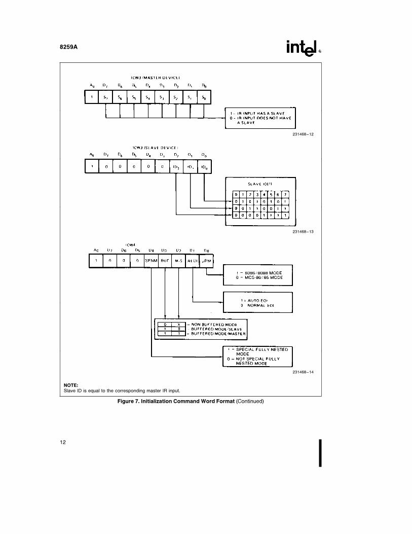
8259A
231468–12
231468–13
231468–14
NOTE:Slave ID is equal to the corresponding master IR input.
Figure 7. Initialization Command Word Format (Continued)
12
8259A
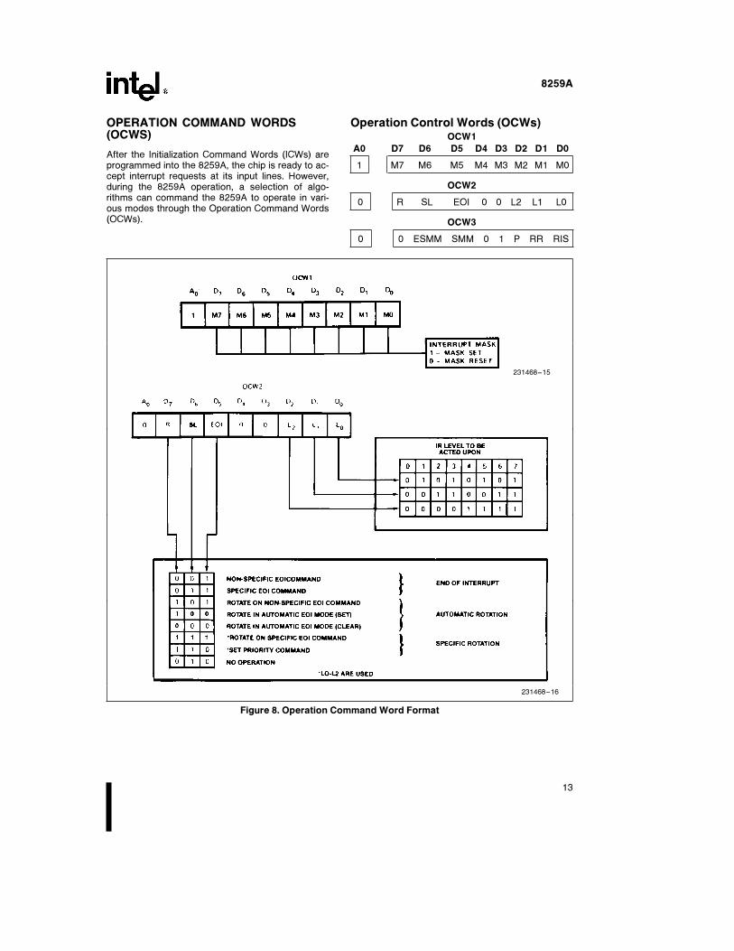
OPERATION COMMAND WORDS(OCWS)
After the Initialization Command Words (ICWs) areprogrammed into the 8259A, the chip is ready to ac-cept interrupt requests at its input lines. However,during the 8259A operation, a selection of algo-rithms can command the 8259A to operate in vari-ous modes through the Operation Command Words(OCWs).
Operation Control Words (OCWs)OCW1
A0 D7 D6 D5 D4 D3 D2 D1 D0
1 M7 M6 M5 M4 M3 M2 M1 M0
OCW2
0 R SL EOI 0 0 L2 L1 L0
OCW3
0 0 ESMM SMM 0 1 P RR RIS
231468–15
231468–16
Figure 8. Operation Command Word Format
13
8259A
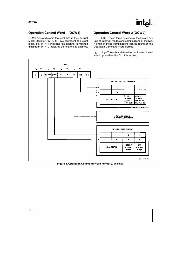
Operation Control Word 1 (OCW1)
OCW1 sets and clears the mask bits in the interruptMask Register (IMR). M7–M0 represent the eightmask bits. M e 1 indicates the channel is masked(inhibited), M e 0 indicates the channel is enabled.
Operation Control Word 2 (OCW2)
R, SL, EOIÐThese three bits control the Rotate andEnd of Interrupt modes and combinations of the two.A chart of these combinations can be found on theOperation Command Word Format.
L2, L1, L0ÐThese bits determine the interrupt levelacted upon when the SL bit is active.
231468–17
Figure 8. Operation Command Word Format (Continued)
14

8259A
Operation Control Word 3 (OCW3)
ESMMÐEnable Special Mask Mode. When this bitis set to 1 it enables the SMM bit to set or reset theSpecial Mask Mode. When ESMM e 0 the SMM bitbecomes a ‘‘don’t care’’.
SMMÐSpecial Mask Mode. If ESMM e 1 and SMMe 1 the 8259A will enter Special Mask Mode. IfESMM e 1 and SMM e 0 the 8259A will revert tonormal mask mode. When ESMM e 0, SMM has noeffect.
Fully Nested Mode
This mode is entered after initialization unless anoth-er mode is programmed. The interrupt requests areordered in priority from 0 through 7 (0 highest).When an interrupt is acknowledged the highest pri-ority request is determined and its vector placed onthe bus. Additionally, a bit of the Interrupt Serviceregister (ISO-7) is set. This bit remains set until themicroprocessor issues an End of Interrupt (EOI)command immediately before returning from theservice routine, or if AEOI (Automatic End of Inter-rupt) bit is set, until the trailing edge of the last INTA.While the IS bit is set, all further interrupts of thesame or lower priority are inhibited, while higher lev-els will generate an interrupt (which will be acknowl-edged only if the microprocessor internal Interuptenable flip-flop has been re-enabled through soft-ware).
After the initialization sequence, IR0 has the highestprioirity and IR7 the lowest. Priorities can bechanged, as will be explained, in the rotating prioritymode.
End of Interrupt (EOI)
The In Service (IS) bit can be reset either automati-cally following the trailing edge of the last in se-quence INTA pulse (when AEOI bit in ICW1 is set) orby a command word that must be issued to the8259A before returning from a service routine (EOIcommand). An EOI command must be issued twiceif in the Cascade mode, once for the master andonce for the corresponding slave.
There are two forms of EOI command: Specific andNon-Specific. When the 8259A is operated in modeswhich perserve the fully nested structure, it can de-termine which IS bit to reset on EOI. When a Non-Specific EOI command is issued the 8259A will auto-matically reset the highest IS bit of those that areset, since in the fully nested mode the highest ISlevel was necessarily the last level acknowledgedand serviced. A non-specific EOI can be issued withOCW2 (EOI e 1, SL e 0, R e 0).
When a mode is used which may disturb the fullynested structure, the 8259A may no longer be ableto determine the last level acknowledged. In thiscase a Specific End of Interrupt must be issuedwhich includes as part of the command the IS levelto be reset. A specific EOI can be issued with OCW2(EOI e 1, SL e 1, R e 0, and L0–L2 is the binarylevel of the IS bit to be reset).
It should be noted that an IS bit that is masked by anIMR bit will not be cleared by a non-specific EOI ifthe 8259A is in the Special Mask Mode.
Automatic End of Interrupt (AEOI)Mode
If AEOI e 1 in ICW4, then the 8259A will operate inAEOI mode continuously until reprogrammed byICW4. in this mode the 8259A will automatically per-form a non-specific EOI operation at the trailingedge of the last interrupt acknowledge pulse (thirdpulse in MCS-80/85, second in 8086). Note thatfrom a system standpoint, this mode should be usedonly when a nested multilevel interrupt structure isnot required within a single 8259A.
The AEOI mode can only be used in a master 8259Aand not a slave. 8259As with a copyright date of1985 or later will operate in the AEOI mode as amaster or a slave.
Automatic Rotation(Equal Priority Devices)
In some applications there are a number of interrupt-ing devices of equal priority. In this mode a device,after being serviced, receives the lowest priority, soa device requesting an interrupt will have to wait, inthe worst case until each of 7 other devices areserviced at most once. For example, if the priorityand ‘‘in service’’ status is:
Before Rotate (IR4 the highest prioirity requiringservice)
‘‘IS’’ Status 231468–18
Priority Status 231468–19
15

8259A
After Rotate (IR4 was serviced, all other prioritiesrotated correspondingly)
‘‘IS’’ Status 231468–20
Priority Status 231468–21
There are two ways to accomplish Automatic Rota-tion using OCW2, the Rotation on Non-Specific EOICommand (R e 1, SL e 0, EOI e 1) and the Ro-tate in Automatic EOI Mode which is set by (R e 1,SL e 0, EOI e 0) and cleared by (R e 0, SL e 0,EOI e 0).
Specific Rotation(Specific Priority)
The programmer can change priorities by program-ming the bottom priority and thus fixing all other pri-orities; i.e., if IR5 is programmed as the bottom prior-ity device, then IR6 will have the highest one.
The Set Priority command is issued in OCW2 where:R e 1, SL e 1, L0–L2 is the binary priority levelcode of the bottom priority device.
Observe that in this mode internal status is updatedby software control during OCW2. However, it is in-dependent of the End of Interrupt (EOI) command(also executed by OCW2). Priority changes can beexecuted during an EOI command by using the Ro-tate on Specific EOI command in OCW2 (R e 1, SLe 1, EOI e 1 and LO–L2 e IR level to receivebottom priority).
Interrupt Masks
Each Interrupt Request input can bem masked indi-vidually by the Interrupt Mask Register (IMR) pro-grammed through OCW1. Each bit in the IMR masksone interrupt channel if it is set (1). Bit 0 masks IR0,Bit 1 masks IR1 and so forth. Masking an IR channeldoes not affect the other channels operation.
Special Mask Mode
Some applications may require an interrupt serviceroutine to dynamically alter the system priority struc-
ture during its execution under software control. Forexample, the routine may wish to inhibit lower priori-ty requests for a portion of its execution but enablesome of them for another portion.
The difficulty here is that if an Interrupt Request isacknowledged and an End of Interrupt command didnot reset its IS bit (i.e., while executing a serviceroutine), the 8259A would have inhibited all lowerpriority requests with no easy way for the routine toenable them.
That is where the Special Mask Mode comes in. Inthe special Mask Mode, when a mask bit is set inOCW1, it inhibits further interrupts at that level andenables interrupts fromall other levels (lower as wellas higher) that are not masked.
Thus, any interrupts may be selectively enabled byloading the mask register.
The special Mask Mode is set by OWC3 where:SSMM e 1, SMM e 1, and cleared where SSMM e
1, SMM e 0.
Poll Command
In Poll mode the INT output functions as it normallydoes. The microprocessor should ignore this output.This can be accomplished either by not connectingthe INT output or by masking interrupts within themicroprocessor, thereby disabling its interrupt input.Service to devices is achieved by software using aPoll command.
The Poll command is issued by setting P e ‘1’’ inOCW3. The 8259A treats the next RD pulse to the8259A (i.e., RD e 0, CS e 0) as an interrupt ac-knowledge, sets the appropriate IS bit if there is arequest, and reads the priority level. Interrupt is fro-zen from WR to RD.
The word enabled onto the data bus during RD is:
D7 D6 D5 D4 D3 D2 D1 D0
I Ð Ð Ð Ð W2 W1 W0
W0–W2: Binary code of the highest priority levelrequesting service.
I: Equal to ‘‘1’’ if there is an interrupt.
This mode is useful if there is a routine commandcommon to several levels so that the INTA se-quence is not needed (saves ROM space). Anotherapplication is to use the poll mode to expand thenumber of priority levels to more than 64.
Reading the 8259A Status
The input status of several internal registers can beread to update the user information on the system.
16
8259A
NOTES:231468–22
1. Master clear active only during ICW1.2. FREEZE is active during INTA and poll sequences only.3. Truth Table for a D-Latch.
C D Q Operation
1 Di Di Follow0 X Qn-1 Hold
Figure 9. Priority CellÐSimplified Logic Diagram
The following registers can be read via OCW3 (IRRand ISR or OCW1 [IMR]).
Interrupt Request Register (IRR): 8-bit register whichcontains the levels requesting an interrupt to be ac-knowledged. The highest request level is reset fromthe IRR when an interrupt is acknowledged. (Not af-fected by IMR.)
In-Service Register (ISR): 8-bit register which con-tains the priority levels that are being serviced. TheISR is updated when an End of Interrupt Commandis issued.
Interrupt Mask Register: 8-bit register which con-tains the interrupt request lines which are masked.
The IRR can be read when, prior to the RD pulse, aRead Register Command is issued with OCW3 (RRe 1, RIS e 0.)
The ISR can be read, when, prior to the RD pulse, aRead Register Command is issued with OCW3 (RRe 1, RIS e 1).
There is no need to write an OCW3 before everystatus read operation, as long as the status readcorresponds with the previous one; i.e., the 8259A‘‘remembers’’ whether the IRR or ISR has been pre-viously selected by the OCW3. This is not true whenpoll is used.
After initialization the 8259A is set to IRR.
For reading the IMR, no OCW3 is needed. The out-put data bus will contain the IMR whenever RD isactive and A0 e 1 (OCW1).
Polling overrides status read when P e 1, RR e 1in OCW3.
Edge and Level Triggered Modes
This mode is programmed using bit 3 in ICW1.
If LTIM e ‘0’, an interrupt request will be recognizedby a low to high transition on an IR input. The IRinput can remain high without generating another in-terrupt.
17

8259A
231468–23
Figure 10. IR Triggering Timing Requirements
If LTIM e ‘1’, an interrupt request will be recognizedby a ‘high’ level on IR Input, and there is no need foran edge detection. The interrupt request must beremoved before the EOI command is issued or theCPU interrupts is enabled to prevent a second inter-rupt from occurring.
The priority cell diagram shows a conceptual circuitof the level sensitive and edge sensitive input circuit-ry of the 8259A. Be sure to note that the requestlatch is a transparent D type latch.
In both the edge and level triggered modes the IRinputs must remain high until after the falling edge ofthe first INTA. If the IR input goes low before thistime a DEFAULT IR7 will occur when the CPU ac-knowledges the interrupt. This can be a useful safe-guard for detecting interrupts caused by spuriousnoise glitches on the IR inputs. To implement thisfeature the IR7 routine is used for ‘‘clean up’’ simplyexecuting a return instruction, thus ignoring the inter-rupt. If IR7 is needed for other purposes a defaultIR7 can still be detected by reading the ISR. A nor-mal IR7 interrupt will set the corresponding ISR bit, adefault IR7 won’t. If a default IR7 routine occurs dur-ing a normal IR7 routine, however, the ISR will re-main set. In this case it is necessary to keep track ofwhether or not the IR7 routine was previously en-tered. If another IR7 occurs it is a default.
The Special Fully Nest Mode
This mode will be used in the case of a big systemwhere cascading is used, and the priority has to beconserved within each slave. In this case the fullynested mode will be programmed to the master (us-
ing ICW4). This mode is similar to the normal nestedmode with the following exceptions:
a. When an interrupt request from a certain slave isin service this slave is not locked out from themaster’s priority logic and further interrupt re-quests from higher priority IR’s within the slavewill be recognized by the master and will initiateinterrupts to the processor. (In the normal nestedmode a slave is masked out when its request is inservice and no higher requests from the sameslave can be serviced.)
b. When exiting the Interrupt Service routine thesoftware has to check whether the interrupt serv-iced was the only one from that slave. This isdone by sending a non-specific End of Interrupt(EOI) command to the slave and then reading itsIn-Service register and checking for zero. If it isempty, a non-specific EOI can be sent to themaster too. If not, no EOI should be sent.
Buffered Mode
When the 8259A is used in a large system wherebus driving buffers are required on the data bus andthe cascading mode is used, there exists the prob-lem of enabling buffers.
The buffered mode will structure the 8259A to sendan enable signal on SP/EN to enable the buffers. Inthis mode, whenever the 8259A’s data bus outputsare enabled, the SP/EN output becomes active.
This modification forces the use of software pro-gramming to determine whether the 8259A is a mas-ter or a slave. Bit 3 in ICW4 programs the bufferedmode, and bit 2 in ICW4 determines whether it is amaster or a slave.
18

8259A
CASCADE MODE
The 8259A can be easily interconnected in a systemof one master with up to eight slaves to handle up to64 priority levels.
The master controls the slaves through the 3 linecascade bus. The cascade bus acts like chip selectsto the slaves during the INTA sequence.
In a cascade configuration, the slave interrupt out-puts are connected to the master interrupt requestinputs. When a slave request line is activated andafterwards acknowledged, the master will enable thecorresponding slave to release the device routineaddress during bytes 2 and 3 of INTA. (Byte 2 onlyfor 8086/8088).
The cascade bus lines are normally low and will con-tain the slave address code from the trailing edge ofthe first INTA pulse to the trailing edge of the thirdpulse. Each 8259A in the system must follow a sep-arate initialization sequence and can be pro-grammed to work in a different mode. An EOI com-mand must be issued twice: once for the master andonce for the corresponding slave. An address de-coder is required to activate the Chip Select (CS)input of each 8259A.
The cascade lines of the Master 8259A are activat-ed only for slave inputs, non-slave inputs leave thecascade line inactive (low).
231468–24
Figure 11. Cascading the 8259A
19

8259A
ABSOLUTE MAXIMUM RATINGS*
Ambient Temperature Under Bias ÀÀÀÀÀÀ0§C to 70§CStorage Temperature ÀÀÀÀÀÀÀÀÀÀb65§C to a150§CVoltage on Any Pin
with Respect to GroundÀÀÀÀÀÀÀÀÀÀb0.5V to a7V
Power Dissipation ÀÀÀÀÀÀÀÀÀÀÀÀÀÀÀÀÀÀÀÀÀÀÀÀÀÀÀ1W
NOTICE: This is a production data sheet. The specifi-cations are subject to change without notice.
*WARNING: Stressing the device beyond the ‘‘AbsoluteMaximum Ratings’’ may cause permanent damage.These are stress ratings only. Operation beyond the‘‘Operating Conditions’’ is not recommended and ex-tended exposure beyond the ‘‘Operating Conditions’’may affect device reliability.
D.C. CHARACTERISTICS TA e 0§C to 70§C, VCC e 5V g 10%
Symbol Parameter Min Max Units Test Conditions
VIL Input Low Voltage b0.5 0.8 V
VIH Input High Voltage 2.0* VCC a 0.5V V
VOL Output Low Voltage 0.45 V IOL e 2.2 mA
VOH Output High Voltage 2.4 V IOH e b400 mA
VOH(INT) Interrupt Output High 3.5 V IOH eb100 mA
Voltage2.4 V IOH e b400 mA
ILI Input Load Current b10 a10 mA 0V s VIN s VCC
ILOL Output Leakage Current b10 a10 mA 0.45V s VOUT s VCC
ICC VCC Supply Current 85 mA
ILIR IR Input Load Current b300 mA VIN e 0
10 mA VIN e VCC
*NOTE:For Extended Temperature EXPRESS VIH e 2.3V.
CAPACITANCE TA e 25§C; VCC e GND e 0V
Symbol Parameter Min Typ Max Unit Test Conditions
CIN Input Capacitance 10 pF fc e 1 MHz
CI/O I/O Capacitance 20 pF Unmeasured Pins Returned to VSS
20

8259A
A.C. CHARACTERISTICS TA e 0§C to 70§C, VCC e 5V g10%
TIMING REQUIREMENTS
Symbol Parameter8259A 8259A-2
Units Test ConditionsMin Max Min Max
TAHRL AO/CS Setup to RD/INTAv 0 0 ns
TRHAX AO/CS Hold after RD/INTAu 0 0 ns
TRLRH RD Pulse Width 235 160 ns
TAHWL AO/CS Setup to WRv 0 0 ns
TWHAX AO/CS Hold after WRu 0 0 ns
TWLWH WR Pulse Width 290 190 ns
TDVWH Data Setup to WRu 240 160 ns
TWHDX Data Hold after WRu 0 0 ns
TJLJH Interrupt Request Width (Low) 100 100 ns See Note 1
TCVIAL Cascade Setup to Second or Third55 40 ns
INTAv (Slave Only)
TRHRL End of RD to Next RD
End of INTA to Next INTA within 160 100 ns
an INTA Sequence Only
TWHWL End of WR to Next WR 190 100 ns
*TCHCL End of Command to Next Command500 150 ns
(Not Same Command Type)
End of INTA Sequence to Next500 300
INTA Sequence.
*Worst case timing for TCHCL in an actual microprocessor system is typically much greater than 500 ns (i.e. 8085A e
1.6 ms, 8085A-2 e 1 ms, 8086 e 1 ms, 8086-2 e 625 ns)
NOTE:This is the low time required to clear the input latch in the edge triggered mode.
TIMING RESPONSES
Symbol Parameter8259A 8259A-2
Units Test ConditionsMin Max Min Max
TRLDV Data Valid from RD/INTAv200 120 ns
C of Data Bus e
100 pF
TRHDZ Data Float after RD/INTAu 10 100 10 85 ns C of Data Bus
TJHIH Interrupt Output Delay 350 300 nsMax Test C e 100 pF
TIALCV Cascade Valid from First INTAv565 360 ns CINT e 100 pF
Min Test C e 15 pF
(Master Only)
TRLEL Enable Active from RDv or INTAv 125 100 nsCCASCADE e 100 pF
TRHEH Enable Inactive from RDu or INTAu 150 150 ns
TAHDV Data Valid from Stable Address 200 200 ns
TCVDV Cascade Valid to Valid Data 300 200 ns
21

8259A
A.C. TESTING INPUT/OUTPUT WAVEFORM
231468–25
A.C. Testing: Inputs are driven at 2.4V for a logic ‘‘1’’ and 0.45Vfor a logic ‘‘0’’. Timing measurements are made at 2.0V for a logic‘‘1’’ and 0.8V for a logic ‘‘0’’.
A.C. TESTING LOAD CIRCUIT
231468–26
CL e 100 pFCL Includes Jig Capacitance
WAVEFORMS
WRITE
231468–27
22
8259A
WAVEFORMS (Continued)
READ/INTA
231468–28
OTHER TIMING
231468–29
23

8259A
WAVEFORMS (Continued)
INTA SEQUENCE
231468–30
NOTES:Interrupt output must remain HIGH at least until leading edge of first INTA.1. Cycle 1 in 8086, 8088 systems, the Data Bus is not active.
Data Sheet Revision Review
The following changes have been made since revision 2 of the 8259A data sheet.
1. The first paragraph of the Poll Command section was rewritten to clarify the status of the INT pin.
2. A paragraph was added to the Interrupt Sequence section to indicate the status of the INT pin duringmultiple interrupts.
3. A reference to PLCC packaging was added.
4. All references to the 8259A-8 have been deleted.
INTEL CORPORATION, 2200 Mission College Blvd., Santa Clara, CA 95052; Tel. (408) 765-8080
INTEL CORPORATION (U.K.) Ltd., Swindon, United Kingdom; Tel. (0793) 696 000
INTEL JAPAN k.k., Ibaraki-ken; Tel. 029747-8511
Printed in U.S.A./xxxx/1196/B10M/xx xx


Telephone: 817-274-7553 �� Fax: 817-548-1358http://www.winsystems.com �� E-mail: [email protected]
WARRANTY
WinSystems warrants that for a period of two (2) years from the date of shipment any Products and Software purchased or licensedhereunder which have been developed or manufactured by WinSystems shall be free of any material defects and shall performsubstantially in accordance with WinSystems' specifications therefore. With respect to any Products or Software purchased orlicensed hereunder which have been developed or manufactured by others, WinSystems shall transfer and assign to Customer anywarranty of such manufacturer or developer held by WinSystems, provided that the warranty, if any, may be assigned. The soleobligation of WinSystems for any breach of warranty contained herein shall be, at its option, either (i) to repair or replace at itsexpense any materially defective Products or Software, or (ii) to take back such Products and Software and refund the Customer thepurchase price and any license fees paid for the same. Customer shall pay all freight, duty, broker's fees, insurance changes and otherfees and charges for the return of any Products or Software to WinSystems under this warranty. WinSystems shall pay freight andinsurance charges for any repaired or replaced Products or Software thereafter delivered to Customer within the United States. Allfees and costs for shipment outside of the United States shall be paid by Customer. The foregoing warranty shall not apply to anyProducts or Software which have been subject to abuse, misuse, vandalism, accidents, alteration, neglect, unauthorized repair orimproper installations.
THERE ARE NO WARRANTIES BY WINSYSTEMS EXCEPT AS STATED HEREIN. THERE ARE NO OTHERWARRANTIES EXPRESS OR IMPLIED INCLUDING, BUT NOT LIMITED TO, THE IMPLIED WARRANTIESOF MERCHANTABILITY AND FITNESS FOR A PARTICULAR PURPOSE, IN NO EVENT SHALLWINSYSTEMS BE LIABLE FOR CONSEQUENTIAL, INCIDENTAL, OR SPECIAL DAMAGES INCLUDING,BUT NOT LIMITED TO, DAMAGES FOR LOSS OF DATA, PROFITS OR GOODWILL. WINSYSTEMS'MAXIMUM LIABILITY FOR ANY BREACH OF THIS AGREEMENT OR OTHER CLAIM RELATED TO ANYPRODUCTS, SOFTWARE, OR THE SUBJECT MATTER HEREOF, SHALL NOT EXCEED THE PURCHASEPRICE OR LICENSE FEE PAID BY CUSTOMER TO WINSYSTEMS FOR THE PRODUCTS OR SOFTWARE ORPORTION THEREOF TO WHICH SUCH BREACH OR CLAIM PERTAINS.
WARRANTY SERVICE
All products returned to WinSystems must be assigned a Return Material Authorization (RMA) number. To obtain this number,please call or FAX WinSystems' factory in Arlington, Texas and provide the following information:
1. Description and quantity of the product(s) to be returned including its serial number.2. Reason for the return.3. Invoice number and date of purchase (if available), and original purchase order number.4. Name, address, telephone and FAX number of the person making the request.5. Do not debit WinSystems for the repair. WinSystems does not authorize debits.
After the RMA number is issued, please return the products promptly. Make sure the RMA number is visible on the outside ofthe shipping package.
The customer must send the product freight prepaid and insured. The product must be enclosed in an anti-static bag to protect itfrom damage caused by static electricity. Each bag must be completely sealed. Packing material must separate each unit returnedand placed as a cushion between the unit(s) and the sides and top of the shipping container. WinSystems is not responsible forany damage to the product due to inadequate packaging or static electricity.