MCDP28x0 DisplayPort1.2a to HDMI2.0 Level … Sheets/MegaChips... · – YCbCr444-to-420...
33
MegaChips’ Proprietary Information Page 1 of 33 MegaChips’ Proprietary Information MegaChips reserves the right to make any change herein at any time without prior notice. MegaChips does not assume any responsibility or liability arising out of application or use of any product or service described herein except as explicitly agreed upon. MCDP28x0 DisplayPort1.2a to HDMI2.0 Level Shifter/Protocol Converter [LSPCON] Datasheet Rev B
Transcript of MCDP28x0 DisplayPort1.2a to HDMI2.0 Level … Sheets/MegaChips... · – YCbCr444-to-420...

MegaChips’ Proprietary Information
Page 1 of 33
MegaChips’ Proprietary Information
MegaChips reserves the right to make any change herein at any time without prior notice. MegaChips
does not assume any responsibility or liability arising out of application or use of any product or
service described herein except as explicitly agreed upon.
MCDP28x0DisplayPort1.2a to HDMI2.0
Level Shifter/Protocol Converter [LSPCON]
Datasheet
Rev B

MCDP28x0
C28x0-DAT-01p MegaChips’ Proprietary Information
Page 2 of 33
Features
• DisplayPort® (DP) ver. 1.2a receiver
– Link rate HBR2/HBR/RBR
– 1, 2, or 4 lanes configuration
– AUX CH 1 Mbps, HPD out
– Supports eDP ASSR scrambler operation
• HDMI ver. 2.0 transmitter
– Max data rate up to 6.0 Gbps/ch
– Deep color up to 16 bits per color
– 3D video timings, CEC, HPD in
– Supports High Dynamic Range (HDR)
– Supports scrambling for the higher data rate
• Level shifter operation (up to 3.4Gbps/ch)
– AC-coupled HDMI1.4b to DC-coupled HDMI1.4b
– PHY analog repeater (re-driver or re-timer)
– 3.3 V DDC/AUX CH signaling support with auto detect
– 3.3 V DDC to 5V DDC buffering
– I2C-over-AUX to 5V DDC translation
– DP HPD_OUT matched to HDMI HPD_IN
• Protocol converter operation (up to 6.0 Gbps/ch)
– DP SST-to-HDMI format conversion
– Video and audio forwarding
– Pixel encoding format conversion from YCbCr444 to YCbCr420
– Horizontal expansion of VESA CVT to CEA-861 timings
– Meta data handing
• Level shifter – Protocol converter mode switching
– Via sideband communication (AUX CH/ DDC)
• Max video resolution and color depth
– 4Kp60Hz, RGB/YCbCr444, 8bpc
– 4Kp60Hz, YCbCr420, up to 16bpc
– 4Kp30Hz, RGB/YCbCr444, up to 16bpc
• YCbCr420 support
– YCbCr444-to-420 conversion, up to 16 bpc
– YCbCr420 pass through, up to 16 bpc
• Stereoscopic 3D forwarding
– Conversion from frame sequential over DP to stacked top-bottom 3D over HDMI
– All other 3D formats forwarded as is
• Audio forwarding
– 2-ch, 768 kHz 24bps HBR audio
– Up to 8-ch, 192 kHz, 24bps LPCM audio, AC3, DTS
• Secure communication
– Intel secure communication protocol compliant with LSPCON spec
• HDCP content protection
– Embedded HDCP keys
– HDCP2.2 transmitter
– HDCP1.x repeater
• Metadata handling
– HDMI TX DVI/HDMI mode setting (DPCD register)
– YCbCr444-420 conversion (DPCD register)
– IEC60958 BYTE3 channel status overwrite
– CEA861F INFOFRAME generation
– CEA861-3 HDR and Mastering InfoFrame
• SCDC read request handling
– Polling enabled for HDMI sinks not supporting read request
• AUX to I2C bridge for EDID/MCCS pass through
• CEC tunneling over AUX CH
• Device configuration options
– SPI flash for firmware binary image storage required
– AUX CH, I2C host interface (optional)
• EMI reduction support
– Spread spectrum for DP input
– Scrambler for DP input and HDMI2.0a output
• Low power operation
– 412 mW in protocol converter mode
– 100 mW in Level shifter mode
– 0.1 mW in connected standby mode
• ESD specification
– +/-6.5 KV HBM, 500 V CDM
• Package
– 64 LFBGA (7 x 7 mm)
• Power supply voltages
– 3.3 V I/O; 1.2 V core

MCDP28x0
C28x0-DAT-01p MegaChips’ Proprietary Information – Strictly Confidential
Page 3 of 33
Applications
• PC notebook/ tablet motherboard
• DP/USB Type-C docking station, dongle
Figure 1. MCDP28x0 internal block diagram
HDMI 2.0Output
DP++ Input
ResetOCMV186
HDMI TransmitterDP Dual ModeReceiver1.2V AC,
5.4Gbps DP to HDMI AV Format Converter
HDCP RX/ TX/Repeater
Analog repeater path
Protocol converter path DC, 3.3V, 6Gbps
AUX/I2C Detector
I2C Level Shifter
I2C bypass path
AUX to I2C Converter
Protocol converter path
HPD 5V SAFE(3.3V IO)
HDMI DDCAUX, AC 3.3V
5V TolI2C DC 3.3V
HPD In
5V Tol
HPD 5V SAFE(3.3V IO)
HPD Out
3.3V TolTo OCMFrom OCM
To / From OCM
Clock Generation
XTAL
TCLK UART_TX
RESETN
GPIOCONFIG
GPIO
I2C Slave
UARTUART_RX
SCL
SDA
SPI ControllerSPI_CLKSPI_DISPI_DOSPI_CSN
CECVDD12_ON
CECVDD12_ON

MCDP28x0
C28x0-DAT-01p MegaChips’ Proprietary Information
Page 4 of 33
Contents
1. Description . . . . . . . . . . . . . . . . . . . . . . . . . . . . . . . . . . . . . . . . . . . . . . . . . 7
2. Application overview . . . . . . . . . . . . . . . . . . . . . . . . . . . . . . . . . . . . . . . . . . 9
2.1 Motherboard-down topology . . . . . . . . . . . . . . . . . . . . . . . . . . . . . . . . . . . . 9
2.2 Adaptor topology . . . . . . . . . . . . . . . . . . . . . . . . . . . . . . . . . . . . . . . . . . . . 9
3. BGA footprint and pin lists . . . . . . . . . . . . . . . . . . . . . . . . . . . . . . . . . . . . . 11
3.1 Ball grid array diagram . . . . . . . . . . . . . . . . . . . . . . . . . . . . . . . . . . . . . . . .11
3.2 Signal mapping sorted by ball (pin) number . . . . . . . . . . . . . . . . . . . . . . . 12
4. Connections . . . . . . . . . . . . . . . . . . . . . . . . . . . . . . . . . . . . . . . . . . . . . . . 14
4.1 Pin list . . . . . . . . . . . . . . . . . . . . . . . . . . . . . . . . . . . . . . . . . . . . . . . . . . . . 14
4.2 Bootstrap configuration . . . . . . . . . . . . . . . . . . . . . . . . . . . . . . . . . . . . . . 18
4.3 RESETN connection . . . . . . . . . . . . . . . . . . . . . . . . . . . . . . . . . . . . . . . . 19
5. Package specifications . . . . . . . . . . . . . . . . . . . . . . . . . . . . . . . . . . . . . . . 20
5.1 Package drawing . . . . . . . . . . . . . . . . . . . . . . . . . . . . . . . . . . . . . . . . . . . 20
5.2 LFBGA 7 x 7 dimensions . . . . . . . . . . . . . . . . . . . . . . . . . . . . . . . . . . . . . 21
5.3 Marking field template and descriptors . . . . . . . . . . . . . . . . . . . . . . . . . . . 21
5.4 Classification reflow profile . . . . . . . . . . . . . . . . . . . . . . . . . . . . . . . . . . . . 22
6. Electrical specifications . . . . . . . . . . . . . . . . . . . . . . . . . . . . . . . . . . . . . . . 23
6.1 Absolute maximum ratings . . . . . . . . . . . . . . . . . . . . . . . . . . . . . . . . . . . . 23
6.2 Power Connections . . . . . . . . . . . . . . . . . . . . . . . . . . . . . . . . . . . . . . . . . 24
6.3 DC characteristics . . . . . . . . . . . . . . . . . . . . . . . . . . . . . . . . . . . . . . . . . . 25
6.4 AC characteristics . . . . . . . . . . . . . . . . . . . . . . . . . . . . . . . . . . . . . . . . . . 26
6.4.1 DisplayPort receiver . . . . . . . . . . . . . . . . . . . . . . . . . . . . . . . . . . . . . . . . 27
6.4.2 HDMI transmitter I/O specifications . . . . . . . . . . . . . . . . . . . . . . . . . . . . 28
6.4.3 I2C interface timing . . . . . . . . . . . . . . . . . . . . . . . . . . . . . . . . . . . . . . . . 29
6.4.4 SPI interface timing . . . . . . . . . . . . . . . . . . . . . . . . . . . . . . . . . . . . . . . . 30
7. Ordering information . . . . . . . . . . . . . . . . . . . . . . . . . . . . . . . . . . . . . . . . . 31
8. Revision history . . . . . . . . . . . . . . . . . . . . . . . . . . . . . . . . . . . . . . . . . . . . . 32

MCDP28x0
C28x0-DAT-01p MegaChips’ Proprietary Information
Page 5 of 33
List of Tables
Table 1. Pin list . . . . . . . . . . . . . . . . . . . . . . . . . . . . . . . . . . . . . . . . . . . . . . . . . . . . . . . . . . . . . . . . . 12Table 2. DisplayPort receiver pins . . . . . . . . . . . . . . . . . . . . . . . . . . . . . . . . . . . . . . . . . . . . . . . . . . 14Table 3. HDMI output pins . . . . . . . . . . . . . . . . . . . . . . . . . . . . . . . . . . . . . . . . . . . . . . . . . . . . . . . . 15Table 4. System interface pins . . . . . . . . . . . . . . . . . . . . . . . . . . . . . . . . . . . . . . . . . . . . . . . . . . . . . 16Table 5. Power and ground pins. . . . . . . . . . . . . . . . . . . . . . . . . . . . . . . . . . . . . . . . . . . . . . . . . . . . 18Table 6. Bootstrap configuration. . . . . . . . . . . . . . . . . . . . . . . . . . . . . . . . . . . . . . . . . . . . . . . . . . . . 18Table 7. Field descriptors . . . . . . . . . . . . . . . . . . . . . . . . . . . . . . . . . . . . . . . . . . . . . . . . . . . . . . . . . 22Table 8. Absolute maximum ratings . . . . . . . . . . . . . . . . . . . . . . . . . . . . . . . . . . . . . . . . . . . . . . . . . 23Table 9. DC characteristics. . . . . . . . . . . . . . . . . . . . . . . . . . . . . . . . . . . . . . . . . . . . . . . . . . . . . . . . 25Table 10. IO DC characteristics . . . . . . . . . . . . . . . . . . . . . . . . . . . . . . . . . . . . . . . . . . . . . . . . . . . . . 25Table 11. Maximum speed of operation . . . . . . . . . . . . . . . . . . . . . . . . . . . . . . . . . . . . . . . . . . . . . . . 26Table 12. DisplayPort receiver characteristics . . . . . . . . . . . . . . . . . . . . . . . . . . . . . . . . . . . . . . . . . . 27Table 13. HDMI transmitter I/O specifications . . . . . . . . . . . . . . . . . . . . . . . . . . . . . . . . . . . . . . . . . . 28Table 14. HDMI transmitter AC characteristics. . . . . . . . . . . . . . . . . . . . . . . . . . . . . . . . . . . . . . . . . . 28Table 15. I2C interface timing. . . . . . . . . . . . . . . . . . . . . . . . . . . . . . . . . . . . . . . . . . . . . . . . . . . . . . . 29Table 16. SPI interface timing, VDD = 3.3 V. . . . . . . . . . . . . . . . . . . . . . . . . . . . . . . . . . . . . . . . . . . . 30Table 17. Order codes . . . . . . . . . . . . . . . . . . . . . . . . . . . . . . . . . . . . . . . . . . . . . . . . . . . . . . . . . . . . 31Table 18. Document revision history . . . . . . . . . . . . . . . . . . . . . . . . . . . . . . . . . . . . . . . . . . . . . . . . . 32

MCDP28x0
C28x0-DAT-01p MegaChips’ Proprietary Information
Page 6 of 33
List of Figures
Figure 1. MCDP28x0 internal block diagram . . . . . . . . . . . . . . . . . . . . . . . . . . . . . . . . . . . . . . . . . . . . 3Figure 2. MCDP2800 motherboard-down use case. . . . . . . . . . . . . . . . . . . . . . . . . . . . . . . . . . . . . . . 9Figure 3. MCDP2850 adaptor (dongle) use case . . . . . . . . . . . . . . . . . . . . . . . . . . . . . . . . . . . . . . . 10Figure 4. MCDP28x0 BGA diagram. . . . . . . . . . . . . . . . . . . . . . . . . . . . . . . . . . . . . . . . . . . . . . . . . . 11Figure 5. RESETN Connection to MCDP28x0. . . . . . . . . . . . . . . . . . . . . . . . . . . . . . . . . . . . . . . . . . 19Figure 6. MCDP28x0 package drawing . . . . . . . . . . . . . . . . . . . . . . . . . . . . . . . . . . . . . . . . . . . . . . . 20Figure 7. MCDP28x0 package dimensions . . . . . . . . . . . . . . . . . . . . . . . . . . . . . . . . . . . . . . . . . . . . 21Figure 8. Marking template . . . . . . . . . . . . . . . . . . . . . . . . . . . . . . . . . . . . . . . . . . . . . . . . . . . . . . . . 22Figure 9. I2C timing . . . . . . . . . . . . . . . . . . . . . . . . . . . . . . . . . . . . . . . . . . . . . . . . . . . . . . . . . . . . . . 29

MCDP28x0
C28x0-DAT-01p MegaChips’ Proprietary Information
Page 7 of 33
1. Description
The MCDP28x0 is a power-optimized DisplayPort1.2a-to-HDMI 2.0 converter device targeted for
desktop/mobile PC motherboard-down applications and for DP or USB type-C adaptor (dongle, docking
station) applications. This device functions as a level shifter as well as an active protocol converter.
In level shifter mode, the device functions as a PHY repeater with optional jitter removal capability. This
operating mode provides a low-power means of using an AC-coupled TMDS signal from a dual mode DP
(DP++) source to be repeated to the HDMI output. The maximum TMDS character clock frequency in this
mode is limited to 340 Mchar/s (per HDMI1.4b specification).
In Protocol Converter (PCON) mode, MCDP28x0 functions as a DP branch device receiving AC coupled
DisplayPort stream and converting it to HDMI output. The maximum TMDS character clock frequency
supported in this mode is up to 600 Mchar/s (as per the HDMI2.0a specification).
The MCDP28x0 operates with two power supply voltages: 1.2 V and 3.3 V. It consumes:
• 100 mW in PHY analog repeater mode
• 412 mW in protocol converter mode
• 0.1 mW in connected standby mode (1.2 V power rail disabled)
The MCDP28x0 has a DisplayPort1.2a dual-mode receiver and HDMI 2.0a transmitter. The upstream
main link can receive DP input at HBR2 rate over 4 lanes and AC-coupled TMDS signal up to
340Mchar/s. It supports DP SST stream on its main link and Manchester-coded AUX signaling or native
3.3 I2C signaling as the side band channel with the DP++ source. The downstream HDMI TX port is
HDMI 2.0 specification compliant.
The MCDP28x0 is capable of supporting Ultra High-Definition video formats, resolutions as high as 4096
x 2160@60 Hz. It supports RGB/YCbCr video color formats with a color depth of 16 bpc (or 48 bits per
pixel) as long as it fits within the DP1.2 and HDMI2.0a link rate. In addition, this device also supports pixel
encoding conversion from YCbCr444 to YCbCr420 and YcbCr420 pass-through from a DP input to an
HDMI output. High Dynamic Range (HDR) with deep color up to 12bpc at 4Kp60Hz is supported through
the conversion of YCbCr444 CVT timing over DP link with horizontal expansion to YCbCr420 CEA timing
on the HDMI TX output.
This device offers secure reception and transmission of high bandwidth digital audio and video content
with HDCP 1.x content protection for the upstream DP interface and HDCP2.2 for the downstream HDMI
interface. It also operates as an HDCP1.x repeater between the source and the sink. In addition, it
conforms to the secure communication protocol specified in the Intel “LSPCON Security Requirements

MCDP28x0
C28x0-DAT-01p MegaChips’ Proprietary Information
Page 8 of 33
Architecture Specification” document. The MCDP28x0 comes with embedded HDCP keys that are stored
in encrypted form.
The MCDP28x0 uses an external crystal of 27 MHz as a reference clock for its operation and it has a
reset input which provides the chip reset during system power up. The device has an on-chip
microcontroller with SPI, UART, and I2C interfaces for system level communication and debug. It
requires an external SPI flash memory for storing device configuration firmware. The firmware update is
done through the DP AUX channel or through UART interface. An 8 Mbit SPI flash memory is
recommended for storing the firmware with a backup option as fail-safe during in-system-programming.

MCDP28x0
C28x0-DAT-01p MegaChips’ Proprietary Information
Page 9 of 33
2. Application overview
Two important target applications of MCDP28x0 are:
• Mobile PC motherboard application. This is referred as motherboard-down topology and the
part number that supports this topology is MCDP2800.
• Accessory application (dongle, docking station etc.). This is referred as adaptor topology and
the part number for this topology is MCDP2850.
2.1 Motherboard-down topology
In a Motherboard-down topology, the MCDP2800 resides next to the source (CPU/GPU) device on a
same PCB with relatively short copper tracks connecting directly to the source. These tracks are typically
micro stripes with controlled impedance of 100 Ω. In this configuration, the source device is aware of the
presence and capabilities of the MCDP2800. The source communicates with MCDP2800 through
AUX/DDC interface via I2C-over-AUX or native I2C (3.3V) messaging. In this topology, typically the
MCDP2800 operates as a re-driving or re-timing analog repeater for AC-coupled TMDS input for speeds
below 3.4Gbps and as a DisplayPort to HDMI protocol converter for speeds above 3.4 Gbps up to 6.0
Gbps. The analog repeater mode saves the active power consumption during low frequency oeprtation.
MCDP2800 however is capable of operating as DP to HDMI protocol converter for the entire operating
range up to 6 Gbps. The motherboard-down topology supports transmitting both HDCP1.x and HDCP2.2
protected content over the HDMI output.
Figure 2. MCDP2800 motherboard-down use case
2.2 Adaptor topology
In an adaptor topology, the MCDP2850 is part of the source side adaptor or docking station that plugs
into the PC/NB via a DP++ connector. In this case, a typical source sends out a DP signal to the adaptor
and the adaptor converts it into HDMI 2.0 output for the entire operating frequency range. However, a
source which is aware of the presence and capabilities of the MCDP2850 can choose to send an AC-
Source SoCMCDP2800 HDMI Sink
HDMI Cable

MCDP28x0
C28x0-DAT-01p MegaChips’ Proprietary Information
Page 10 of 33
coupled TMDS signal at lower speeds (below 3.4 Gbps) and a DP signal at higher speeds (above 3.4
Gbps) similar to a motherboard-down topology. In the adaptor application, the MCDP2850 dynamically
decides whether to use I2C-over-AUX or native I2C messaging at the time of connectivity with the
source. MCDP2850 only supports HDCP1.x repeater/transmitter functionality; no HDCP2.2 transmitter
function allowed in this topology.
Note: In an adaptor topology, signal degradation is higher compared to in a motherboard-down topology due to longer traces and multiple connectors in the path.
Figure 3. MCDP2850 adaptor (dongle) use case
DongleSource SoC
MCDP2850 HDMI Sink
HDMI Cable

MCDP28x0
C28x0-DAT-01p MegaChips’ Proprietary Information
Page 11 of 33
3. BGA footprint and pin lists
3.1 Ball grid array diagram
The ball grid array (BGA) diagrams give the allocation of signals to the balls of the package, shown from
the top looking down using the PCB footprint.
Some signal names in BGA diagrams have been abbreviated. Refer to the pin list for full signal names
sorted by pin number.
Figure 4. MCDP28x0 BGA diagram
A
B
C
D
E
F
G
H
1 2 3 4 5 6 7 8
1 2 3 4 5 6 7 8
A
B
C
D
E
F
G
H
DPRXL3N
DPRXL3P
DPRXHPD_OUT
VDD33RX GND VDD12
RXVDD12
RX GND VDD12PLL RESETN
SPI_CSN SPI_DI GPIO1 VDD33RX
VDD33AUX R_EXT DPRX
AUXPDPRXAUXN
SPI_DO SPI_CLK VDD33IO GND GND VDD12
DIG UART_TX TEST
HDMITXDDC_SCL SPI_WP VDD33
IO GND GND I2C_SDA UART_RX XT
HDMITXDDC_SDA
HDMICEC CONFIG1 VDD12
OSCVDD12
DIG I2C_SCL C_EXT
HDMITXHPD_IN
VDD33TX GND VDD33
TXVDD12
TX GND VDD12TX
VDD12ON
HDMITXCLKN
HDMITXCLKP
HDMITXCH0N
HDMITXCH0P
HDMITXCH1N
HDMITXCH1P
HDMITXCH2N
HDMITXCH2P
DPRXL2N
DPRXL2P
DPRXL1N
DPRXL1P
DPRXL0N
DPRXL0P
HDMI_TX DP_RX SYS_DIGITAL SYS_ANALOG
Power ReturnPower 1.2VPower 3.3V 8kV pads

MCDP28x0
C28x0-DAT-01p MegaChips’ Proprietary Information
Page 12 of 33
3.2 Signal mapping sorted by ball (pin) number
Table 1. Pin list
Pin number Net name
A1 DPRX_L3N
A2 DPRX_L3P
A3 DPRX_L2N
A4 DPRX_L2P
A5 DPRX_L1N
A6 DPRX_L1P
A7 DPRX_L0N
A8 DPRX_L0P
B1 DPRX_HPD_OUT
B2 VDD33_RX
B3 GND
B4 VDD12_RX
B5 VDD12_RX
B6 GND
B7 VDD12_PLL
B8 RESETN
C1 SPI_CSN
C2 SPI_DI
C3 GPIO1
C4 VDD33_RX
C5 VDD33_AUX
C6 R_EXT
C7 DPRX_AUXP
C8 DPRX_AUXN
D1 SPI_DO
D2 SPI_CLK
D3 VDD33_IO
D4 GND
D5 GND
D6 VDD12_DIG
D7 UART_TX
D8 TEST
E1 HDMITX_DDC_SCL
E2 SPI_WP

MCDP28x0
C28x0-DAT-01p MegaChips’ Proprietary Information
Page 13 of 33
E3 VDD33_IO
E4 GND
E5 GND
E6 I2C_SDA
E7 UART_RX
E8 XTAL
F1 HDMITX_DDC_SDA
F2 HDMI_CEC
F3 CONFIG1
F4 VDD12_OSC
F5 VDD12_DIG
F6 I2C_SCL
F7 C_EXT
F8 TCLK
G1 HDMITX_HPD_IN
G2 VDD33_TX
G3 GND
G4 VDD33_TX
G5 VDD12_TX
G6 GND
G7 VDD12_TX
G8 VDD12_ON
H1 HDMITX_CLKN
H2 HDMITX_CLKP
H3 HDMITX_CH0N
H4 HDMITX_CH0P
H5 HDMITX_CH1N
H6 HDMITX_CH1P
H7 HDMITX_CH2N
H8 HDMITX_CH2P
Table 1. Pin list (continued)
Pin number Net name

MCDP28x0
C28x0-DAT-01p MegaChips’ Proprietary Information
Page 14 of 33
4. Connections
4.1 Pin list
I/O Legend:
I = Input; O = Output; P = Power; G = Ground; IO = Bi-direction; AI = Analog input
Table 2. DisplayPort receiver pins
Pin Assignment I/OVDD Domain
Description
A1 DPRX_L3N I 1.2 V
DisplayPort receiver main link Lane 3 negative analog input.
AC-coupled internal pull up to VDD12_RX through 50 Ω resistor.
A2 DPRX_L3P I 1.2 V
DisplayPort receiver main link Lane 3 positive analog input.
AC-coupled internal pull up to VDD12_RX through 50 Ω resistor.
A3 DPRX_L2N I 1.2 V
DisplayPort receiver main link Lane 2 negative analog input.
AC-coupled internal pull up to VDD12_RX through 50 Ω resistor.
A4 DPRX_L2P I 1.2 V
DisplayPort receiver main link Lane 2 positive analog input.
AC-coupled internal pull up to VDD12_RX through 50 Ω resistor.
A5 DPRX_L1N I 1.2 V
DisplayPort receiver main link Lane 1 negative analog input.
AC-coupled internal pull up to VDD12_RX through 50 Ω resistor.
A6 DPRX_L1P I 1.2 V
DisplayPort receiver main link Lane 1 positive analog input.
AC-coupled internal pull up to VDD12_RX through 50 Ω resistor.
A7 DPRX_L0N I 1.2 V
DisplayPort receiver main link Lane 0 negative analog input.
AC-coupled internal pull up to VDD12_RX through 50 Ω resistor.
A8 DPRX_L0P I 1.2 V
DisplayPort receiver main link Lane 0 positive analog input.
AC-coupled internal pull up to VDD12_RX through 50 Ω resistor.

MCDP28x0
C28x0-DAT-01p MegaChips’ Proprietary Information
Page 15 of 33
Table 3. HDMI output pins
C7 DPRX_AUXP IO 3.3 V
DisplayPort receiver auxiliary channel positive analog input/output. Common mode voltage = 3.3 V
AC-coupled internal pull up to VDD33_AUX through 50 Ω resistor. Also functions as DDC_SCL.
C8 DPRX_AUXN IO 3.3V
DisplayPort receiver auxiliary channel negative analog input/output. Common mode voltage = 3.3 V
AC-coupled internal pull up to VDD33_AUX through 50 Ω resistor. Also functions as DDC_SDA.
B1 DPRX_HPD_OUT O 3.3 VTo the upstream HPD signal pin (DP source), to be externally pulled down (100K ohm recommended) as per DP1.2a spec.
C6 R_EXT IO 1.2 VTermination calibration reference resistor; 249 Ω 1% resistor should be connected from this pin to VDD12_RX (1.2 V analog power supply).
F3 CONFIG1 IO 3.3V
General purpose IO. Connects to DP upstream connector pin 13 in Adaptor topology. Optional in Motherboard-down topology. Default POR state is INPUT use weak pull-down when not used.
Pin Assignment I/OVDD Domain
Description
H1 HDMITX_CLKN O 3.3 V HDMI transmitter CLOCK_N to TX connector
H2 HDMITX_CLKP O 3.3 V HDMI transmitter CLOCK_P to TX connector
H3 HDMITX_CH0N O 3.3 V HDMI transmitter DATA0_N to TX connector
H4 HDMITX_CH0P O 3.3 V HDMI transmitter DATA0_P to TX connector
H5 HDMITX_CH1N O 3.3 V HDMI transmitter DATA1_N to TX connector
H6 HDMITX_CH1P O 3.3 V HDMI transmitter DATA1_P to TX connector
H7 HDMITX_CH2N O 3.3 V HDMI transmitter DATA2_N to TX connector
H8 HDMITX_CH2P O 3.3 V HDMI transmitter DATA2_P to TX connector
Pin Assignment I/OVDD Domain
Description

MCDP28x0
C28x0-DAT-01p MegaChips’ Proprietary Information
Page 16 of 33
Table 4. System interface pins
E1 HDMITX_DDC_SCL O3.3 V, 5 V Tol
HDMI TX DDC I2C master SCL. 3.3 V logic level, 5 V tolerant. Open drain, external 2.2 K pull up to +5 V.
F1 HDMITX_DDC_SDA IO3.3 V, 5 V Tol
HDMI TX DDC I2C master SDA. 3.3 V logic level, 5 V tolerant. Open drain, external 2.2 K pull up to +5 V.
F2 HDMI_CEC IO 3.3 VCEC input. 3.3 V open drain IO. Connect to HDMI CEC pin, to be externally pulled up to 3.3 V (27K Ohm recommended) as per HDMI1.4b spec.
G1 HDMITX_HPD_IN I3.3 V, 5 V Tol
3.3 V logic level, 5 V tolerant input from HDMI connector. To be externally pulled down via resistor. (47K Ohm recommended)
Pin Assignment I/OVDD
DomainReset State Description
B8 RESETN I 3.3 V Input
Power-ON chip reset (active low) input signal
Connects to 3.3V VDD through 2.2K +/-10% resistor
E8 XTAL IO 1.2 V NAConnect to 27 MHz crystal oscillator with 22 pF to VDD12_OSC
F8 TCLK IO 1.2 V NAConnect to 27 MHz crystal oscillator with 22 pF to VDD12_OSC
F7 C_EXT O 3.3V NACapacitor for filtering internal 2.5V LDOR. Connect to GND through 2.2uF capacitor.
G8 VDD12_ON O 3.3 V Output
1.2 V power control signal to control external 1.2 V power as shown in Figure 4. Reset State definition
assumes 3.3 V Rail is ramped up to full voltage.
Pin Assignment I/OVDD Domain
Description

MCDP28x0
C28x0-DAT-01p MegaChips’ Proprietary Information
Page 17 of 33
D8 TEST IO 3.3 V NATest select. Tie to GND for mission mode
E6 I2C_SDA IO 3.3 VInput, Internal PU
Host I2C interface data line. External pull-up required for I2C operation.
Leave NC when not used.
F6 I2C_SCL I 3.3 VInput, Internal PU
Host I2C interface clock line. External pull-up required for I2C operation.
Leave NC when not used.
C3 GPIO1 IO 3.3 VInput, Internal PU
General purpose input/output. Applicable for CONFIG2 if needed. Default POR state is INPUT; use weak pull-down when not used.
C1 SPI_CSN O 3.3 VInput, Internal PU
Serial peripheral interface chip select
C2 SPI_DI I
3.3 VInput, Internal PD
Serial peripheral interface data input
D1 SPI_DO O
3.3 VInput, Internal PD
Serial peripheral interface data output
D2 SPI_CLK O 3.3 VInput, Internal PD
Serial peripheral interface clock
E2 SPI_WP O 3.3 VInput, Internal PD
Serial peripheral interface write protect
D7 UART_TX O 3.3 VInput, Internal PU
Universal asynchronous serial Tx output.
Leave NC when not used.
Pin Assignment I/OVDD
DomainReset State Description

MCDP28x0
C28x0-DAT-01p MegaChips’ Proprietary Information
Page 18 of 33
Table 5. Power and ground pins
4.2 Bootstrap configuration
Other than the normal operating mode (mission mode), the MCDP28x0 is configured in testing and
debugging mode during factory testing and chip bring-up. For this purpose, the chip is configured during
the boot operation using several bootstrap configurations. DC levels on these bootstrap pins are latched
during the de-asserting edge of power-on reset (RESETN goes HIGH). The levels specified below must
be adhered to for the normal function of the device.
Table 6. Bootstrap configuration
E7 UART_RX I 3.3 VInput, Internal PU
Universal asynchronous serial Rx input.
Leave NC when not used.
Pin Assignment Voltage Level Description
B2, C4 VDD33_RX L3.3 V DisplayPort RX analog power
B4, B5 VDD12_RX 1.2 V DisplayPort RX analog power
C5 VDD33_AUX 3.3 V DisplayPort AUX analog power
B7 VDD12_PLL 1.2 V PLL analog power
F4 VDD12_OSC 1,2 V Oscillator circuit power
G2, G4 VDD33_TX 3.3 V HDMI TX analog power
G5, G7 VDD12_TX 1.2 V HDMI TX analog power
D6, F5 VDD12_DIG 1.2 V Core and 1.2V IO power
D3, E3 VDD33_IO 3.3 V 3.3V IO power
B3, B6, D4, D5, E4, E5, G3, G6
GND GND Power return for all supplies
Bootstrap signal name
Internal PU/PD Pin assignment Function
Bootstrap_0 PULL UP UART_TX (D7)
0: Reserved for ATE test
1: Normal operation (mission mode)
Pin Assignment I/OVDD
DomainReset State Description

MCDP28x0
C28x0-DAT-01p MegaChips’ Proprietary Information
Page 19 of 33
Note: When the pin corresponding to a specific bootstrap is left NC, the pin takes the value of the assigned by the internal PULLUP (Level 1) or PULLDN (Level 0). The internal resistor used is around 50 k Ω. To select a non-default value on a bootstrap, an external PULLUP or PULLDN resistor tied to the opposite direction that overcomes the internal PULLUP or PULLDN needs to be used.
4.3 RESETN connection
The RESETN pin must be pulled up to 3.3 V via a 2.2 kohm +/- 10% resistor as shown below. The chip
also supports an active low, external reset pulse to RESETN allowing a system host controller to reset
the system. The recommended way to drive RESETN is through an open-drain output. Alternately, if an
open-drain output is not available, the series resistor shown in the figure below is required.
Figure 5. RESETN Connection to MCDP28x0
Bootstrap_1 PULL DN SPI_WP (E2)
0: Normal operation (mission mode)
1: OCM debug mode
Bootstrap_2 PULL DN SPI_CLK (D2)
0: (Default) Internal ROM is enabled and mapped to top 32 K of OCM memory map. OCM boots from IROM. Normal mode (mission mode).
1: Internal ROM is disabled. External ROM includes the address range reserved for IROM. OCM boots from EXTROM. Debug mode.
Bootstrap_3 PULL DN SPI_DO (D1)
0: Default. Reserved (mission mode)
1: Reserved for testing
Bootstrap_4 PULL UP SPI_CSN (C1)
0: Select external CLK on XTAL pin (used in ATE).
1: (Default) Select crystal and internal oscillator. Normal operation (mission mode).
System Host
External Reset Control (optional)
3.3V
MCDP28x0
RESETNExternal Reset
Switch (for debug)External 1.5K to 3Kohm +/‐1% series resistor
2.2Kohm
Capacitor Value should not exceed
50pF

MCDP28x0
C28x0-DAT-01p MegaChips’ Proprietary Information
Page 20 of 33
5. Package specifications
Package type: LFBGA (7 x 7 x 1.4 mm, 64 F8 x 8 Pitch 0.8 Ball 0.4)
5.1 Package drawing
Figure 6. MCDP28x0 package drawing

MCDP28x0
C28x0-DAT-01p MegaChips’ Proprietary Information
Page 21 of 33
5.2 LFBGA 7 x 7 dimensions
Figure 7. MCDP28x0 package dimensions
5.3 Marking field template and descriptors
The MCDP28x0 marking template is shown below.
DIMENSIONS
DATABOOK (mm)
DRAWING (mm)
REF. MIN. TYP. MAX. MIN. TYP. MAX. NOTES
A 1.4 1.24 (1)A1 0.25 0.25 0.30 0.35A2 0.29 0.24 0.28 0.32A4 0.60 0.57 0.585 0.60b 0.35 0.40 0.45 0.35 0.40 0.45 (2)D 6.95 7.00 7.05 6.95 7.00 7.05
D1 5.60 5.60E 6.95 7.00 7.05 6.95 7.00 7.05E1 5.60 5.60e 0.80 0.80Z 0.70 0.70
ddd 0.08 0.08eee 0.09 0.09 (4)fff 0.05 0.05 (5)
NOTES:
(1) - LFBGA stands for Low profile Fine Pitch Ball Grid Array. - Thin profile: 1.00mm < A 1.20mm / Fine pitch: e < 1.00mm pitch. - The total profile height (Dim A) is measured from the seating plane to the top of the component - The maximum total package height is calculated by the following methodology: A Max = A1 Typ + A2 Typ + A4 Typ + (A1² + A2² + A4² tolerance values)
(2) – The typical ball diameter before mounting is 0.40mm.
(3) – LFBGA with 0.40mm pitch is not yet registered into JEDEC Publications.
(4) - The tolerance of position that controls the location of the pattern of balls with respect to datums A and B. For each ball there is a cylindrical tolerance zone eee perpendicular to datum C and located on true position with respect to datums A and B as defined by e. The axis perpendicular to datum C of each ball must lie within this tolerance zone.
(5) - The tolerance of position that controls the location of the balls within the matrix with respect to each other. For each ball there is a cylindrical tolerance zone fff perpendicular to datum C and located on true position as defined by e. The axis perpendicular to datum C of each ball must lie within this tolerance zone. Each tolerance zone fff in the array is contained entirely in the respective zone eee above The axis of each ball must lie simultaneously in both tolerance zones.
(6) - The terminal A1 corner must be identified on the top surface by using a corner chamfer, ink or metallized markings, or other feature of package body or integral heatslug. - A distinguishing feature is allowable on the bottom surface of the package to identify the terminal A1
corner. Exact shape of each corner is optional.

MCDP28x0
C28x0-DAT-01p MegaChips’ Proprietary Information
Page 22 of 33
Figure 8. Marking template
Field descriptors are shown below.
5.4 Classification reflow profile
Please refer to the DisplayPort Application Note: Classification reflow profile for SMD devices (C0353-APN-06) for reflow diagram and details.
Table 7.Field descriptors
Field Description Marking
A MegaChips logo MegaChips
B Product code
One of the codes below:
MCDP2800BB
MCDP2850BB
MCDP2800BC
MCDP2850BC
C 2-character diffusion plant code VQ
D 3-digit wafer start date “YWW”
E 3-character FE sequence code “ABC”
F 2-character assembly plant code 99
G 3-character BE sequence code “XYZ”
H Optional marking <blank> or ES(1)
1. Marked ES for Engineering Samples, used for development purposes.
I 3-character country of origin code MYS
J 2-digit test plant code 8U
K 1-digit assembly year “Y”
L 2-digit assembly week “WW”
M Ball A1 identifier a DOT

MCDP28x0
C28x0-DAT-01p MegaChips’ Proprietary Information
Page 23 of 33
6. Electrical specifications
6.1 Absolute maximum ratings
Applied conditions greater than those listed under “Absolute maximum ratings” may cause permanent
damage to the device. The device should never exceed absolute maximum conditions since it may affect
device reliability.
Table 8. Absolute maximum ratings
Note (1): All voltages are measured with respect to GND.
Note (2): Absolute maximum voltage ranges are for transient voltage excursions.
Note (3): For connector facing pins CONFIG1 and DPRX_HPD_OUT, a series resistor of 100 ohms is recommended. Refer to the MCDP28x0 Layout Guideline appnote.
Note (4): JEDEC Class1.
Note (5): These are simulated results under the following conditions: Four layer JEDEC PCB, no heat spreader, Air flow = 0 m/s.
Parameter Symbol Min Typ Max Units
3.3 V supply voltages (1,2) VVDD_3.3 -0.3 3.3 3.96 V
1.2 V supply voltages (1.2) VVDD_1.2 -0.3 1.2 1.44 V
Input voltage tolerance for 3.3 V, 5 V tolerant I/O pins VIN5tol -0.3 5.5 V
Input voltage tolerance for 3.3 V I/O pins VIN3V3 -0.3 3.63 V
ESD – Human Body Model (HBM) [JESD22-A114 spec] For all pins
VESD +/- 2.0 kV
ESD – Human Body Model (HBM) [IEC61000-4 spec]
For DP and HDMI connector-facing pinsVESD - - +/- 6.5 kV
ESD – Charged Device Model (CDM) VESD - - +/- 500 V
Latch-up (3,4) ILA - - +/- 100 mA
Ambient operating temperature TA 0 - 70 C
Storage temperature TSTG -40 - 150 C
Operating junction temperature TJ 0 75 125 C
Thermal resistance (Junction to Ambient)(5) JA - - 49.0 C/W
Thermal resistance (Junction to Case)(5) JC - - 20.1 C/W
Peak IR reflow soldering temperature TSOL - - 260 C

MCDP28x0
C28x0-DAT-01p MegaChips’ Proprietary Information
Page 24 of 33
6.2 Power Connections
MCDP28x0
REXT
VDD33_RX
249ohm/1%
0.1uF
0.1uF
VDD12_TX
VDD12_RX
VDD33_TX
VDD12_OSC
VDD12_PLLTCLK
XTAL
0.1uF22pF
22pF
GND
VDD33_IO
VDD12_DIG
22pF
0.1uF
0.1uF
0.1uF
From 3.3V regulator
0.1uF
CEXT
2.2uF
0.1uF
VDD12ON0.01uF
R1
R2V_ON
V_OUTGND
V_IN1.2V REGULATOR
B2D3
E3VDD33_IO
G2
G4VDD33_TX
0.1uF0.1uF
VDD33_RXC4
C6
VDD12_RXB4
B5
F4
F8
E8
B3, B6, D4, D5, E4, E5, G3, G6, D8
F7VDD12_DIG
D6
F5B7
VDD12_TXG5
G7
0.1uF
0.1uF
G8
VDD33_AUXC5
FB= FERRITE BEAD 120Ohms@100MHz
FB FB
FB
FBFB
FBFB

MCDP28x0
C28x0-DAT-01p MegaChips’ Proprietary Information
Page 25 of 33
6.3 DC characteristics
Table 9. DC characteristics
Note: Ripple amplitude for power supplies should be 30 mV or lower with max ripple frequency of up to 30 MHz.
Table 10. IO DC characteristics
Parameter Symbol Min Typ Max Units
3.3 V supply voltages (analog and digital) VVDD_3.3 3.14 3.3 3.47 V
1.2 V supply voltages (analog and digital) VVDD_1.2 1.14 1.2 1.26 V
Power
Protocol converter Mode
Measurement condition:
Nominal corner, 25°C, Nominal power supply
4k x 2k / 60 Hz 4L HBR2 to HDMI test pattern: ON-OFF dot Moire attributes-based rendering
412 460 mW
Analog PHY repeater mode 100 120 mW
Sleep State 18 20 mW
Connected standby mode 0.1 0.2 mW
Supply current
Measurement conditions:
Nominal corner, 25°C, Nominal power supply
4k x 2k @60 MHz
4L HBR to HDMI2.0a
VDD (analog and digital) 3.3V
VDD (analog and digital) 1.2V
30
300
mA
Parameter Symbol Min Typ Max Units
Inputs 3.3 V IO signals, 5 V tolerant open drain type
High voltage VIH 2.0 5.5 V
Low voltage VIL -0.3 0.8 V
Input Hysteresis voltage VHYST 300 mV
High current (VIN = 3.3 V) IIH +/- 10 A
Low current (VIN = 0.8 V) IIL +/- 10 A
Input capacitance CIN 5 pF
Outputs 3.3 V IO signals, 5 V tolerant open drain type
MCDP28x0
C28x0-DAT-01p MegaChips’ Proprietary Information
Page 26 of 33
6.4 AC characteristics
Low Current (VOL = 0.2 V) IOL 4 mA
Tri-state leakage current IOZ 10 A
VDD12_ON output
Output Low Voltage (IOL=0.25mA) VOL 0.4 V
Output High Voltage(IOH=0.25mA) VOH 2.9 V
Low Level output Current IOL 0.25
High Level Output Current IOH 0.25
Inputs 3.3 V IO signals, 3.3 V tolerant, TRISTATE
High voltage VIH 2.0 V
Low voltage VIL 0.8 V
Input Hysteresis voltage VHYST 300 mV
High current (VIN = 3.3 V) IIH ±10 A
Low current (VIN = 0.8 V) IIL ±10 A
Input capacitance CIN 1.0 pF
Outputs 3.3 V IO signals, 3.3 V tolerant, TRISTATE
RoutOutput Impedance,
VOL=0.3V50 Ω
Rout
Output Impedance,
VDDE3V3-0.3V
50 Ω
Tri-state leakage current IOZ ±10 A
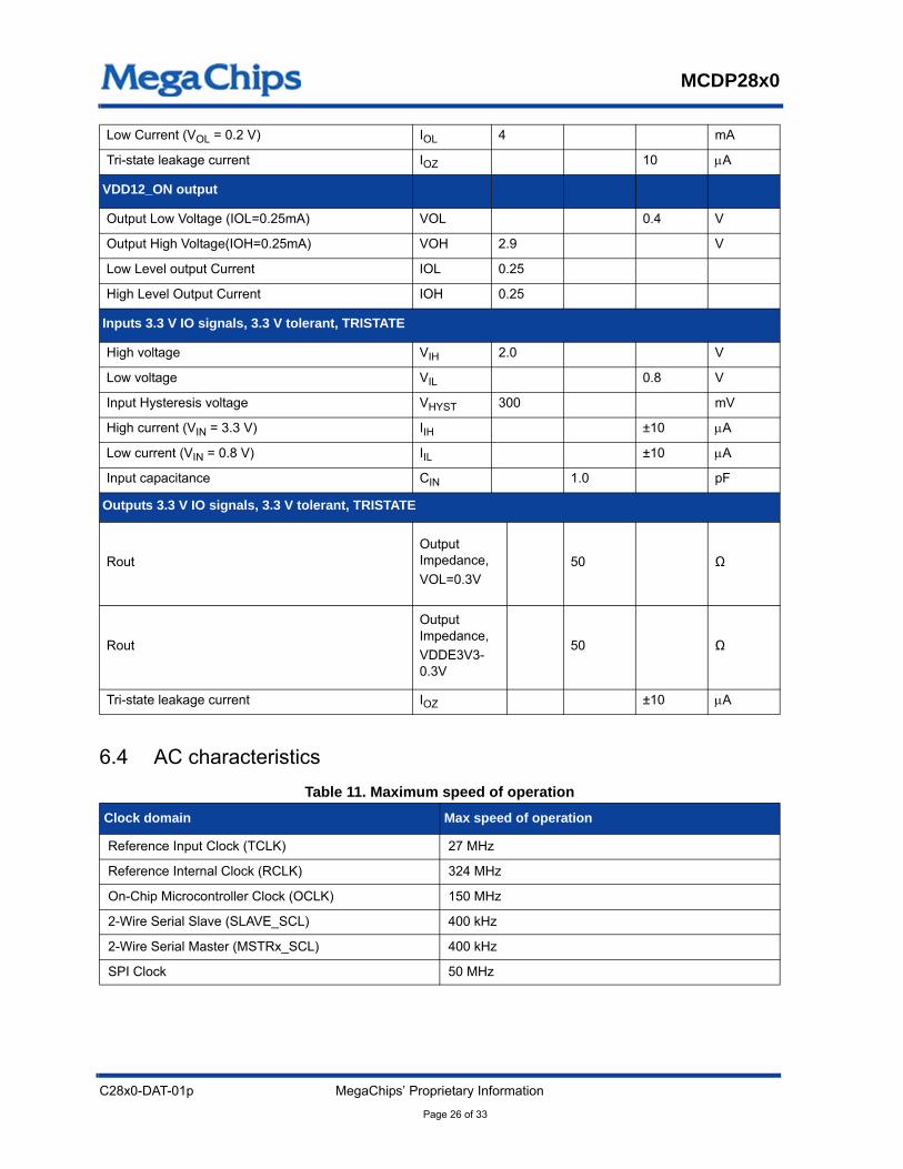
Table 11. Maximum speed of operation
Clock domain Max speed of operation
Reference Input Clock (TCLK) 27 MHz
Reference Internal Clock (RCLK) 324 MHz
On-Chip Microcontroller Clock (OCLK) 150 MHz
2-Wire Serial Slave (SLAVE_SCL) 400 kHz
2-Wire Serial Master (MSTRx_SCL) 400 kHz
SPI Clock 50 MHz

MCDP28x0
C28x0-DAT-01p MegaChips’ Proprietary Information
Page 27 of 33
6.4.1 DisplayPort receiver
Table 12. DisplayPort receiver characteristics
Parameter Symbol Min Typ Max Units Comments
Receiver operating range
Differential Input Voltage RangeVRX_DIF_PP_RANG
E0.04~1 V
RX Termination Control Range RRX_TERM_RANGE 80 ~120 ohm
DisplayPort receiver system parameters
HBR2 unit interval (5.4Gbps) UIHBR2 185 ps
HBR unit interval (2.7Gbps) UIHBR 370 ps
RBR unit interval (1.62Gbps) UIRBR 617 ps
Link clock down spreading 0 0.5 %Modulation frequency range 0f 30 kHz to 33 kHz
DisplayPort receiver TP3 parameters
Receiver Eye TP3 RBR TRBR_EYE_TP3 0.25 UI @ 40mV V_diff_pp
Receiver Eye TP3_EQ HBR THBR_EYE_TP3EQ 0.4 UI @ 135mV V_diff_pp
Receiver Eye TP3_EQ HBR2 THBR2_EYE_TP3EQ 0.3 UI @ 70mV V_diff_pp
Lane intra-pair skew tolerance
TSKEW_INTRA_RBR 260 psSkew contribution from the cable in addition to the stressed EYE at TP3.
TSKEW_INTRA_HBR 60 ps
TSKEW_INTRA_HBR2 50 ps
DJ Non-ISI at 1.62 Gbps TRX_DJ_RBR 0.186 UI1.62Gbps signal @ package pins
DJ Non-ISI at 2.7 Gbps TRX_DJ_HBR 0.339 UI2.7Gbps signal @ package pins
DJ at 5.4 Gbps TRX_DJ_HBR2 0.57 UI5.4 Gbps signal @ package pins
TJ at 1.62 Gbps TRX_TJ_RBR 0.78 UI1.62Gbps signal @ package pins
TJ at 2.7 Gbps TRX_TJ_HBR 0.53 UI2.7Gbps signal @ package pins
TJ at 5.4 Gbps TRX_TJ_HBR2 0.7 UI5.4 Gbps signal @ package pins

MCDP28x0
C28x0-DAT-01p MegaChips’ Proprietary Information
Page 28 of 33
6.4.2 HDMI transmitter I/O specifications
Table 13. HDMI transmitter I/O specifications
Table 14. HDMI transmitter AC characteristics
AUX parameters
Differential Input Voltage Range
VAUX_RX_DIF_RANG
E0.14~1 V
RX Termination Control Range RAUX_TERM_RANGE 40~60 ohms
AUX TX peak-peak Range VAUX_TX_DIF_PP 0~1 V7.8125mV/step in 128 steps
Parameters Symbol Min Typ Max Unit Comments
Differential output: single ended swing amplitude
VTX_PP 0.4 0.5 0.6 V
Differential output: Differential swing amplitude
VTX_DIF_PP 0.8 1 1.2 V
Differential high level output VTX_DIF_HIGH 3.12 3.3 3.49 V
Differential low level output VTX_DIF_LOW 3.12 3.49 V
Parameters Symbol Min Typ Max Unit Comments
TMDS Character Clock fTX_CHR_CLK 25 600 MHz Programmable
Differential Output Voltage VTX_DIF_PP 0 1200 mV In 128 steps
TX Edge Rate tTX_ER 75 145 pS1V VTX_DIF_PP and Premphasis at 0dB in 8 steps
TX Pre-Emphasis Level APREMPH 0 6 dB1V VTX_DIF_PP in 16 steps
TX Termination Control Range RTX_TERM_RANGE 100 600 ohmsProgrammable Termination
TX Jitter <1.65Gbps for Pattern
D10.2TTX_J_D102_LF 60 pS
TX Jitter <1.65Gbps for PatternPRBS7
TTX_J_PRBS7_LF 70 pS
TX Jitter >1.65Gbps, < 3.4Gbps for PatternD10.2
TTX_J_D102_MF 35 pS
TX Jitter >1.65Gbps, < 3.4Gbps for PatternPRBS7
TTX_J_PRBS7_MF 45 pS
Parameter Symbol Min Typ Max Units Comments

MCDP28x0
C28x0-DAT-01p MegaChips’ Proprietary Information
Page 29 of 33
6.4.3 I2C interface timing
Table 15. I2C interface timing
Note: The maximum tHD;DAT only has to be met if the device does not stretch the low period tLOW of the SCL signal. In the diagram below, S = start, P = stop, Sr = Repeated start, and SP= Repeated stop conditions.
Figure 9. I2C timing
TX Jitter >3.4Gbps for PatternD10.2
TTX_J_D102_HF 30 pS
TX Jitter >3.4Gbps for PatternPRBS7
TTX_J_PRBS7_HF 35 pS
Symbol Parameter Conditions Min Typ Max Unit
fSCL SCL clock rate Fast mode 0 - 400 kHz
tHD-STA Hold time STARTAfter this period, the 1st clock starts
1.2 - - s
tLOW Low period of clock SCL 1.3 - - s
tHIGH High period of clock SCL 1.2 - - s
Tsu;STASet up time for a repeated START
1.2 - - s
tHD;DAT Data hold time For master 0.7 - 0.9(1) s
tSU;DAT Data setup time 380 - - ns
TBUFBus free time between STOP and START
1.3 - - s
CbCapacitance load for each bus line
- 100 400 pF
tr Rise time 220 - 300 ns
tf Fall time 60 - 300 ns
VnhNoise margin at high level
0.25VDD - - V
VnlNoise margin at low level
0.2VDD - -
SDA
SCL
tf
S
tLOW trtftSU;DAT tHD;STA tSP tr tBUF
SPtHD;STA tHD;DAT tHIGH
tSU;STASr
tSU;STO

MCDP28x0
C28x0-DAT-01p MegaChips’ Proprietary Information
Page 30 of 33
6.4.4 SPI interface timing
Table 16. SPI interface timing, VDD = 3.3 V
Symbol Parameter Min Typ Max Units
FCLK SPI_CLK output clock frequency 50 MHz
TSCKH Serial clock high time 20 ns
TSCKL Serial clock low time 20 ns
TR_SPI_CLK SPI_CLK rise time @10mA drive 10pF load 2.8 ns
TF_SPI_CLK SPI_CLK fall time @10mA drive 10pF load 3.2 ns
TMEM_CLK_F Device speed 75 MHz
TMEM_CSN_SU Device CSN input setup time requirement 7 ns
TMEM_CSN_HLD Device CSN input setup time requirement 7 ns
TMEM_DO_PD Device DO out propagation delay 6 ns
TMEM_DI_SU Device DI setup time 3 ns
TMEM_DI_SU Device DI hold time 5 ns

MCDP28x0
C28x0-DAT-01p MegaChips’ Proprietary Information
Page 31 of 33
7. Ordering information
Table 17. Order codes
Part number Description
MCDP2800-BBES64 LFBGA (7 x 7 x 1.4 mm) for motherboard-down application. Engineering samples, for development purpose only. (Rev BB silicon)
MCDP2800-BB64 LFBGA (7 x 7 x 1.4 mm) for motherboard-down application. Mass production parts. Delivered in trays. (Rev BB silicon)
MCDP2800-BBT64 LFBGA (7 x 7 x 1.4 mm) for motherboard-down application. Mass production parts. Delivered in tape and reel. (Rev BB silicon)
MCDP2850-BB64 LFBGA (7 x 7 x 1.4 mm) for dongle application. Delivered in trays. (Rev BB silicon)
MCDP2850-BBT64 LFBGA (7 x 7 x 1.4 mm) for dongle application. Delivered in tape and reel. (Rev BB silicon)
MCDP2800-BC64 LFBGA (7 x 7 x 1.4 mm) for motherboard-down application. Mass production parts. Delivered in trays. (Rev BC silicon)
MCDP2800-BCT64 LFBGA (7 x 7 x 1.4 mm) for motherboard-down application. Mass production parts. Delivered in tape and reel. (Rev BC silicon)
MCDP2850-BC64 LFBGA (7 x 7 x 1.4 mm) for dongle application. Delivered in trays. (Rev BC silicon)
MCDP2850-BCT64 LFBGA (7 x 7 x 1.4 mm) for dongle application. Delivered in tape and reel. (Rev BC silicon)

MCDP28x0
C28x0-DAT-01p MegaChips’ Proprietary Information
Page 32 of 33
8. Revision history
Table 18. Document revision history
Date Revision Changes
09-Mar-2016 A Initial version.
07-Apr-2016 BUpdated HDMI2.0 to HDMI2.0a throughout the datasheet. Added sub-bullet to Features section.

MCDP28x0
C28x0-DAT-01p MegaChips’ Proprietary Information
Page 33 of 33
Notice
Semiconductor products may possibly experience breakdown or malfunction. Adequate care should be taken with respect to the safety design of equipment in order to prevent the occurrence of human injury, fire or social loss in the event of breakdown or malfunction of semiconductor products
The overview of operations and illustration of applications described in this document indicate the conceptual method of use of the semiconductor product and do not guarantee operability in equipment in which the product is actually used.
The names of companies and trademarks stated in this document are registered trademarks of the relevant companies.
MegaChips Co. provides no guarantees nor grants any implementation rights with respect to industrial property rights, intellectual property rights and other such rights belonging to third parties or/and MegaChips Co. in the use of products and of technical information including information on the overview of operations and the circuit diagrams that are described in this document.
The product described in this document may possibly be considered goods or technology regulated by the Foreign Currency and Foreign Trade Control Law. In the event such law applies, export license will be required under said law when exporting the product. This regulation shall be valid in Japan domestic.
In the event the intention is to use the product described in this document in applications that require an extremely high standard of reliability such as nuclear systems, aerospace equipment or medical equipment for life support, please contact the sales department of MegaChips Co. in advance.
All information contained in this document is subject to change without notice.
Copyright ©2016 MegaChips Corporation All rights reserved
MegaChips CorporationHead Quarters1-1-1 Miyahara, Yodogawa-ku Osaka 532-0003, JapanTEL: +81-6-6399-2884
MegaChips Corporation Taiwan BranchRM. B 2F, Worldwide House, No.129,Min Sheng E. Rd., Sec. 3, Taipei 105, TaiwanTEL: +886-2-2547-1297
MegaChips CorporationTokyo Office17-6 Ichiban-cho, Chiyoda-ku, Tokyo 102-0082, JapanTEL: +81-3-3512-5080
MegaChips CorporationTainan OfficeRM. 2, 8F, No.24, Da Qiao 2 Rd., Yong Kang Dist.,Tainan 710, TaiwanTEL: +886-6-302-2898
MegaChips Corporation Makuhari Office1-3 Nakase Mihama-ku Chiba 261-8501, JapanTEL: +81-43-296-7414
MegaChips Corporation Zhunan OfficeNo.118, Chung-Hua Rd., Chu-Nan, Miao-Li 350, TaiwanTEL: +886-37-666-156
MegaChips CorporationSan Jose Office2033 Gateway Place, Suite 400, San Jose, CA 95110 U.S.A.TEL: +1-408-570-0555
MegaChips Corporation Shenzhen OfficeRoom 6307, Office Tower, Shun Hing Square, 5002Shen Nan Dong Road, Luohu District,Shenzhen 518000, P. R. ChinaTEL: +86-755-3664-6990
MegaChips CorporationIndia Branch17th Floor, Concorde Block UB City,Vittal Mallya Road, Bangalore 560-001, IndiaTEL: +91-80-4041-3999