MC9S08QE128, MC9S08QE96, MC9S08QE64 - …HCS08 Microcontrollers freescale.com M MC9S08QE128...
346
HCS08 Microcontrollers freescale.com M MC9S08QE128 MC9S08QE96 MC9S08QE64 Reference Manual MC9S08QE128RM Rev. 2 6/2007 Related Documentation: • MC9S08QE128 (Data Sheet) Contains pin assignments and diagrams, all electrical specifications, and mechanical drawing outlines. Find the most current versions of all documents at: http://www.freescale.com
Transcript of MC9S08QE128, MC9S08QE96, MC9S08QE64 - …HCS08 Microcontrollers freescale.com M MC9S08QE128...

HCS08Microcontrollers
freescale.com
M
MC9S08QE128MC9S08QE96MC9S08QE64Reference Manual
MC9S08QE128RMRev. 26/2007
Related Documentation:
• MC9S08QE128 (Data Sheet)Contains pin assignments and diagrams, all electricalspecifications, and mechanical drawing outlines.
Find the most current versions of all documents at:
http://www.freescale.com

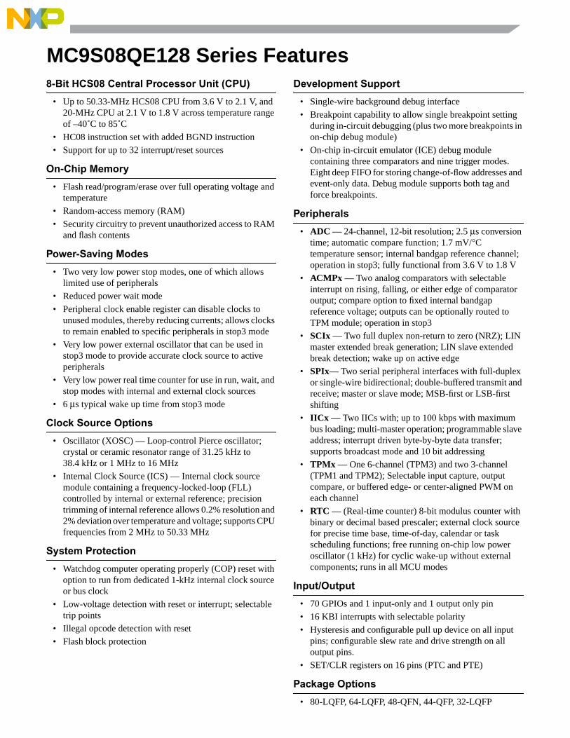
MC9S08QE128 Series Features8-Bit HCS08 Central Processor Unit (CPU)
• Up to 50.33-MHz HCS08 CPU from 3.6 V to 2.1 V, and20-MHz CPU at 2.1 V to 1.8 V across temperature rangeof –40˚C to 85˚C
• HC08 instruction set with added BGND instruction
• Support for up to 32 interrupt/reset sources
On-Chip Memory
• Flash read/program/erase over full operating voltage andtemperature
• Random-access memory (RAM)
• Security circuitry to prevent unauthorized access to RAMand flash contents
Power-Saving Modes
• Two very low power stop modes, one of which allowslimited use of peripherals
• Reduced power wait mode
• Peripheral clock enable register can disable clocks tounused modules, thereby reducing currents; allows clocksto remain enabled to specific peripherals in stop3 mode
• Very low power external oscillator that can be used instop3 mode to provide accurate clock source to activeperipherals
• Very low power real time counter for use in run, wait, andstop modes with internal and external clock sources
• 6 μs typical wake up time from stop3 mode
Clock Source Options
• Oscillator (XOSC) — Loop-control Pierce oscillator;crystal or ceramic resonator range of 31.25 kHz to38.4 kHz or 1 MHz to 16 MHz
• Internal Clock Source (ICS) — Internal clock sourcemodule containing a frequency-locked-loop (FLL)controlled by internal or external reference; precisiontrimming of internal reference allows 0.2% resolution and2% deviation over temperature and voltage; supports CPUfrequencies from 2 MHz to 50.33 MHz
System Protection
• Watchdog computer operating properly (COP) reset withoption to run from dedicated 1-kHz internal clock sourceor bus clock
• Low-voltage detection with reset or interrupt; selectabletrip points
• Illegal opcode detection with reset
• Flash block protection
Development Support
• Single-wire background debug interface
• Breakpoint capability to allow single breakpoint settingduring in-circuit debugging (plus two more breakpoints inon-chip debug module)
• On-chip in-circuit emulator (ICE) debug modulecontaining three comparators and nine trigger modes.Eight deep FIFO for storing change-of-flow addresses andevent-only data. Debug module supports both tag andforce breakpoints.
Peripherals
• ADC — 24-channel, 12-bit resolution; 2.5 μs conversiontime; automatic compare function; 1.7 mV/°Ctemperature sensor; internal bandgap reference channel;operation in stop3; fully functional from 3.6 V to 1.8 V
• ACMPx — Two analog comparators with selectableinterrupt on rising, falling, or either edge of comparatoroutput; compare option to fixed internal bandgapreference voltage; outputs can be optionally routed toTPM module; operation in stop3
• SCIx — Two full duplex non-return to zero (NRZ); LINmaster extended break generation; LIN slave extendedbreak detection; wake up on active edge
• SPIx— Two serial peripheral interfaces with full-duplexor single-wire bidirectional; double-buffered transmit andreceive; master or slave mode; MSB-first or LSB-firstshifting
• IICx — Two IICs with; up to 100 kbps with maximumbus loading; multi-master operation; programmable slaveaddress; interrupt driven byte-by-byte data transfer;supports broadcast mode and 10 bit addressing
• TPMx — One 6-channel (TPM3) and two 3-channel(TPM1 and TPM2); Selectable input capture, outputcompare, or buffered edge- or center-aligned PWM oneach channel
• RTC — (Real-time counter) 8-bit modulus counter withbinary or decimal based prescaler; external clock sourcefor precise time base, time-of-day, calendar or taskscheduling functions; free running on-chip low poweroscillator (1 kHz) for cyclic wake-up without externalcomponents; runs in all MCU modes
Input/Output
• 70 GPIOs and 1 input-only and 1 output only pin
• 16 KBI interrupts with selectable polarity
• Hysteresis and configurable pull up device on all inputpins; configurable slew rate and drive strength on alloutput pins.
• SET/CLR registers on 16 pins (PTC and PTE)
Package Options
• 80-LQFP, 64-LQFP, 48-QFN, 44-QFP, 32-LQFP

Get the latest version from freescale.com
MC9S08QE128 Reference ManualCovers MC9S08QE128
MC9S08QE96MC9S08QE64
MC9S08QE128RMRev. 26/2007
Freescale™ and the Freescale logo are trademarks of Freescale Semiconductor, Inc.
© Freescale Semiconductor, Inc., 2007. All rights reserved.

Revision History
To provide the most up-to-date information, the revision of our documents on the World Wide Web will bethe most current. Your printed copy may be an earlier revision. To verify you have the latest informationavailable, refer to:
http://freescale.com/
The following revision history table summarizes changes contained in this document.
RevisionNumber
RevisionDate Description of Changes
1 30 Apr 2007 Initial preliminary release
2 25 Jun 2007 Initial public release
© Freescale Semiconductor, Inc., 2007. All rights reserved.
This product incorporates SuperFlash® Technology licensed from SST.

List of Chapters
Chapter 1 Device Overview ..............................................................................19
Chapter 2 Pins and Connections.....................................................................25
Chapter 3 Modes of Operation.........................................................................39
Chapter 4 Memory.............................................................................................51
Chapter 5 Resets, Interrupts, and General System Control..........................89
Chapter 6 Parallel Input/Output Control........................................................111
Chapter 7 Keyboard Interrupt (S08KBIV2) ....................................................139
Chapter 8 Central Processor Unit (S08CPUV4)............................................145
Chapter 9 Analog Comparator 3V (ACMPVLPV1) ........................................167
Chapter 10 Analog-to-Digital Converter (S08ADC12V1)................................175
Chapter 11 Internal Clock Source (S08ICSV3) ...............................................203
Chapter 12 Inter-Integrated Circuit (S08IICV2) ...............................................217
Chapter 13 Real-Time Counter (S08RTCV1) ...................................................237
Chapter 14 Serial Communications Interface (S08SCIV4).............................247
Chapter 15 Serial Peripheral Interface (S08SPIV3) ........................................267
Chapter 16 Timer/Pulse-Width Modulator (S08TPMV3) .................................283
Chapter 17 Development Support ...................................................................307
Chapter 18 Debug Module (DBG) (128K).........................................................321
MC9S08QE128 MCU Series Reference Manual, Rev. 2
Freescale Semiconductor 7


Contents
Section Number Title Page
Chapter 1Device Overview
1.1 Devices in the MC9S08QE128 Series .............................................................................................191.2 MCU Block Diagram ......................................................................................................................201.3 System Clock Distribution ..............................................................................................................23
Chapter 2Pins and Connections
2.1 Device Pin Assignment ...................................................................................................................252.2 Recommended System Connections ...............................................................................................31
2.2.1 Power ................................................................................................................................332.2.2 Oscillator ...........................................................................................................................332.2.3 RESET and RSTO ............................................................................................................332.2.4 Background / Mode Select (BKGD/MS) ..........................................................................342.2.5 ADC Reference Pins (VREFH, VREFL) ..............................................................................352.2.6 General-Purpose I/O and Peripheral Ports ........................................................................35
Chapter 3Modes of Operation
3.1 Introduction .....................................................................................................................................393.2 Features ...........................................................................................................................................393.3 Run Mode ........................................................................................................................................39
3.3.1 Low Power Run Mode (LPRun) .......................................................................................393.4 Active Background Mode ................................................................................................................413.5 Wait Mode .......................................................................................................................................42
3.5.1 Low Power Wait Mode (LPWait) ......................................................................................423.6 Stop Modes ......................................................................................................................................42
3.6.1 Stop2 Mode .......................................................................................................................433.6.2 Stop3 Mode .......................................................................................................................443.6.3 Active BDM Enabled in Stop Mode .................................................................................453.6.4 LVD Enabled in Stop Mode ..............................................................................................453.6.5 Stop modes in Low Power Run Mode ..............................................................................45
3.7 Mode Selection ................................................................................................................................453.7.1 On-Chip Peripheral Modules in Stop and Low Power Modes ..........................................48
Chapter 4Memory
4.1 MC9S08QE128 Series Memory Map .............................................................................................514.2 Reset and Interrupt Vector Assignments .........................................................................................53
MC9S08QE128 MCU Series Reference Manual, Rev. 2
Freescale Semiconductor 9

Section Number Title Page
4.3 Register Addresses and Bit Assignments ........................................................................................554.4 Memory Management Unit .............................................................................................................63
4.4.1 Features .............................................................................................................................634.4.2 Register Definition ............................................................................................................634.4.3 Functional Description ......................................................................................................66
4.5 RAM ................................................................................................................................................694.6 Flash ................................................................................................................................................69
4.6.1 Features .............................................................................................................................704.6.2 Register Descriptions ........................................................................................................704.6.3 Functional Description ......................................................................................................774.6.4 Operating Modes ...............................................................................................................864.6.5 Flash Module Security ......................................................................................................864.6.6 Resets ................................................................................................................................88
Chapter 5Resets, Interrupts, and General System Control
5.1 Introduction .....................................................................................................................................895.2 Features ...........................................................................................................................................895.3 MCU Reset ......................................................................................................................................895.4 Computer Operating Properly (COP) Watchdog .............................................................................905.5 Interrupts .........................................................................................................................................91
5.5.1 Interrupt Stack Frame .......................................................................................................925.5.2 External Interrupt Request (IRQ) Pin ...............................................................................925.5.3 Interrupt Vectors, Sources, and Local Masks ....................................................................93
5.6 Low-Voltage Detect (LVD) System ................................................................................................965.6.1 Power-On Reset Operation ...............................................................................................965.6.2 Low-Voltage Detection (LVD) Reset Operation ...............................................................965.6.3 Low-Voltage Detection (LVD) Interrupt Operation ..........................................................965.6.4 Low-Voltage Warning (LVW) Interrupt Operation ...........................................................96
5.7 Peripheral Clock Gating ..................................................................................................................965.8 Reset, Interrupt, and System Control Registers and Control Bits ...................................................98
5.8.1 Interrupt Pin Request Status and Control Register (IRQSC) ............................................985.8.2 System Reset Status Register (SRS) .................................................................................995.8.3 System Background Debug Force Reset Register (SBDFR) ..........................................1005.8.4 System Options Register 1 (SOPT1) ..............................................................................1015.8.5 System Options Register 2 (SOPT2) ..............................................................................1025.8.6 System Device Identification Register (SDIDH, SDIDL) ..............................................1035.8.7 System Power Management Status and Control 1 Register (SPMSC1) .........................1045.8.8 System Power Management Status and Control 2 Register (SPMSC2) .........................1055.8.9 System Power Management Status and Control 3 Register (SPMSC3) .........................1065.8.10 System Clock Gating Control 1 Register (SCGC1) ........................................................1075.8.11 System Clock Gating Control 2 Register (SCGC2) ........................................................108
MC9S08QE128 MCU Series Reference Manual, Rev. 2
10 Freescale Semiconductor

Section Number Title Page
Chapter 6Parallel Input/Output Control
6.1 Port Data and Data Direction ........................................................................................................1116.2 Pull-up, Slew Rate, and Drive Strength .........................................................................................112
6.2.1 Port Internal Pull-Up Enable ...........................................................................................1126.2.2 Port Slew Rate Enable ....................................................................................................1126.2.3 Port Drive Strength Select ...............................................................................................112
6.3 Port Data Set, Clear and Toggle Data Registers ............................................................................1136.3.1 Port Data Set Registers ...................................................................................................1146.3.2 Port Data Clear Registers ................................................................................................1146.3.3 Port Data Toggle Register ...............................................................................................114
6.4 Pin Behavior in Stop Modes ..........................................................................................................1146.5 Parallel I/O and Pin Control Registers ..........................................................................................114
6.5.1 Port A Registers ..............................................................................................................1156.5.2 Port B Registers ..............................................................................................................1176.5.3 Port C Registers ..............................................................................................................1196.5.4 Port D Registers ..............................................................................................................1236.5.5 Port E Registers ...............................................................................................................1256.5.6 Port F Registers ...............................................................................................................1296.5.7 Port G Registers ..............................................................................................................1316.5.8 Port H Registers ..............................................................................................................1336.5.9 Port J Registers ...............................................................................................................135
Chapter 7Keyboard Interrupt (S08KBIV2)
7.1 Introduction ...................................................................................................................................1397.1.1 KBI Clock Gating ...........................................................................................................1397.1.2 Features ...........................................................................................................................1397.1.3 Modes of Operation ........................................................................................................1397.1.4 Block Diagram ................................................................................................................140
7.2 External Signal Description ..........................................................................................................1407.3 Register Definition ........................................................................................................................141
7.3.1 KBI Interrupt Status and Control Register (KBIxSC) ....................................................1417.3.2 KBI Interrupt Pin Select Register (KBIxPE) ..................................................................1427.3.3 KBI Interrupt Edge Select Register (KBIxES) ...............................................................142
7.4 Functional Description ..................................................................................................................1427.4.1 Edge Only Sensitivity .....................................................................................................1437.4.2 Edge and Level Sensitivity ..............................................................................................1437.4.3 Pull-Up/Pull-Down Resistors ..........................................................................................1437.4.4 Keyboard Interrupt Initialization ....................................................................................143
MC9S08QE128 MCU Series Reference Manual, Rev. 2
Freescale Semiconductor 11
Section Number Title Page
Chapter 8Central Processor Unit (S08CPUV4)
8.1 Introduction ...................................................................................................................................1458.1.1 Features ...........................................................................................................................145
8.2 Programmer’s Model and CPU Registers .....................................................................................1468.2.1 Accumulator (A) .............................................................................................................1468.2.2 Index Register (H:X) .......................................................................................................1468.2.3 Stack Pointer (SP) ...........................................................................................................1478.2.4 Program Counter (PC) ....................................................................................................1478.2.5 Condition Code Register (CCR) .....................................................................................147
8.3 Addressing Modes .........................................................................................................................1498.3.1 Inherent Addressing Mode (INH) ...................................................................................1498.3.2 Relative Addressing Mode (REL) ...................................................................................1498.3.3 Immediate Addressing Mode (IMM) ..............................................................................1498.3.4 Direct Addressing Mode (DIR) ......................................................................................1508.3.5 Extended Addressing Mode (EXT) ................................................................................1508.3.6 Indexed Addressing Mode ..............................................................................................150
8.4 Special Operations .........................................................................................................................1518.4.1 Reset Sequence ...............................................................................................................1518.4.2 Interrupt Sequence ..........................................................................................................1518.4.3 Wait Mode Operation ......................................................................................................1528.4.4 Stop Mode Operation ......................................................................................................1528.4.5 BGND Instruction ...........................................................................................................153
8.5 HCS08 Instruction Set Summary ..................................................................................................155
Chapter 9Analog Comparator 3V (ACMPVLPV1)
9.1 Introduction ...................................................................................................................................1679.1.1 ACMP Configuration Information ..................................................................................1679.1.2 ACMP/TPM Configuration Information .........................................................................1679.1.3 ACMP Clock Gating .......................................................................................................1679.1.4 Interrupt Vectors ..............................................................................................................1689.1.5 Features ...........................................................................................................................1709.1.6 Modes of Operation ........................................................................................................1709.1.7 Block Diagram ................................................................................................................170
9.2 External Signal Description ..........................................................................................................1719.3 Register Definition ........................................................................................................................171
9.3.1 ACMPx Status and Control Register (ACMPxSC) .........................................................1729.4 Functional Description ..................................................................................................................173
MC9S08QE128 MCU Series Reference Manual, Rev. 2
12 Freescale Semiconductor
Section Number Title Page
Chapter 10Analog-to-Digital Converter (S08ADC12V1)
10.1 Introduction ...................................................................................................................................17510.1.1 ADC Clock Gating ..........................................................................................................17510.1.2 Module Configurations ...................................................................................................17710.1.3 Features ...........................................................................................................................17910.1.4 Block Diagram ................................................................................................................179
10.2 External Signal Description ..........................................................................................................18010.2.1 Analog Power (VDDAD) ..................................................................................................18110.2.2 Analog Ground (VSSAD) .................................................................................................18110.2.3 Voltage Reference High (VREFH) ...................................................................................18110.2.4 Voltage Reference Low (VREFL) .....................................................................................18110.2.5 Analog Channel Inputs (ADx) ........................................................................................181
10.3 Register Definition ........................................................................................................................18110.3.1 Status and Control Register 1 (ADCSC1) ......................................................................18110.3.2 Status and Control Register 2 (ADCSC2) ......................................................................18310.3.3 Data Result High Register (ADCRH) .............................................................................18410.3.4 Data Result Low Register (ADCRL) ..............................................................................18410.3.5 Compare Value High Register (ADCCVH) ....................................................................18510.3.6 Compare Value Low Register (ADCCVL) .....................................................................18510.3.7 Configuration Register (ADCCFG) ................................................................................18510.3.8 Pin Control 1 Register (APCTL1) ..................................................................................18710.3.9 Pin Control 2 Register (APCTL2) ..................................................................................18810.3.10Pin Control 3 Register (APCTL3) ..................................................................................189
10.4 Functional Description ..................................................................................................................19010.4.1 Clock Select and Divide Control ....................................................................................19010.4.2 Input Select and Pin Control ...........................................................................................19110.4.3 Hardware Trigger ............................................................................................................19110.4.4 Conversion Control .........................................................................................................19110.4.5 Automatic Compare Function .........................................................................................19410.4.6 MCU Wait Mode Operation ............................................................................................19410.4.7 MCU Stop3 Mode Operation ..........................................................................................19410.4.8 MCU Stop1 and Stop2 Mode Operation .........................................................................195
10.5 Initialization Information ..............................................................................................................19510.5.1 ADC Module Initialization Example .............................................................................195
10.6 Application Information ................................................................................................................19710.6.1 External Pins and Routing ..............................................................................................19710.6.2 Sources of Error ..............................................................................................................199
MC9S08QE128 MCU Series Reference Manual, Rev. 2
Freescale Semiconductor 13

Section Number Title Page
Chapter 11Internal Clock Source (S08ICSV3)
11.1 Introduction ...................................................................................................................................20311.1.1 External Oscillator ..........................................................................................................20311.1.2 Stop2 Mode Considerations ............................................................................................20311.1.3 Features ...........................................................................................................................20511.1.4 Block Diagram ................................................................................................................20511.1.5 Modes of Operation ........................................................................................................206
11.2 External Signal Description ..........................................................................................................20711.3 Register Definition ........................................................................................................................207
11.3.1 ICS Control Register 1 (ICSC1) .....................................................................................20811.3.2 ICS Control Register 2 (ICSC2) .....................................................................................20911.3.3 ICS Trim Register (ICSTRM) .........................................................................................20911.3.4 ICS Status and Control (ICSSC) .....................................................................................210
11.4 Functional Description ..................................................................................................................21211.4.1 Operational Modes ..........................................................................................................21211.4.2 Mode Switching ..............................................................................................................21411.4.3 Bus Frequency Divider ...................................................................................................21511.4.4 Low Power Bit Usage .....................................................................................................21511.4.5 DCO Maximum Frequency with 32.768 kHz Oscillator ................................................21511.4.6 Internal Reference Clock ................................................................................................21511.4.7 External Reference Clock ...............................................................................................21611.4.8 Fixed Frequency Clock ...................................................................................................21611.4.9 Local Clock .....................................................................................................................216
Chapter 12Inter-Integrated Circuit (S08IICV2)
12.1 Introduction ...................................................................................................................................21712.1.1 Module Configuration .....................................................................................................21712.1.2 Interrupt Vectors ..............................................................................................................21712.1.3 Features ...........................................................................................................................21912.1.4 Modes of Operation ........................................................................................................21912.1.5 Block Diagram ................................................................................................................220
12.2 External Signal Description ..........................................................................................................22012.2.1 SCL — Serial Clock Line ...............................................................................................22012.2.2 SDA — Serial Data Line ................................................................................................220
12.3 Register Definition ........................................................................................................................22112.3.1 IIC Address Register (IICxA) .........................................................................................22112.3.2 IIC Frequency Divider Register (IICxF) .........................................................................22212.3.3 IIC Control Register (IICxC1) ........................................................................................22412.3.4 IIC Status Register (IICxS) .............................................................................................22512.3.5 IIC Data I/O Register (IICxD) ........................................................................................226
MC9S08QE128 MCU Series Reference Manual, Rev. 2
14 Freescale Semiconductor
Section Number Title Page
12.3.6 IIC Control Register 2 (IICxC2) .....................................................................................22712.4 Functional Description ..................................................................................................................228
12.4.1 IIC Protocol .....................................................................................................................22812.4.2 10-bit Address .................................................................................................................23212.4.3 General Call Address ......................................................................................................233
12.5 Resets ............................................................................................................................................23312.6 Interrupts .......................................................................................................................................233
12.6.1 Byte Transfer Interrupt ....................................................................................................23312.6.2 Address Detect Interrupt .................................................................................................23312.6.3 Arbitration Lost Interrupt ................................................................................................233
12.7 Initialization/Application Information ..........................................................................................235
Chapter 13Real-Time Counter (S08RTCV1)
13.1 Introduction ...................................................................................................................................23713.1.1 ADC Hardware Trigger ..................................................................................................23713.1.2 RTC Clock Sources .........................................................................................................23713.1.3 RTC Modes of Operation ................................................................................................23713.1.4 RTC Clock Gating ...........................................................................................................23713.1.5 Interrupt Vector ...............................................................................................................23813.1.6 Features ...........................................................................................................................24013.1.7 Modes of Operation ........................................................................................................24013.1.8 Block Diagram ................................................................................................................241
13.2 External Signal Description ..........................................................................................................24113.3 Register Definition ........................................................................................................................241
13.3.1 RTC Status and Control Register (RTCSC) ....................................................................24213.3.2 RTC Counter Register (RTCCNT) ..................................................................................24313.3.3 RTC Modulo Register (RTCMOD) ................................................................................243
13.4 Functional Description ..................................................................................................................24413.4.1 RTC Operation Example .................................................................................................245
13.5 Initialization/Application Information ..........................................................................................245
Chapter 14Serial Communications Interface (S08SCIV4)
14.1 Introduction ...................................................................................................................................24714.1.1 SCI Clock Gating ............................................................................................................24714.1.2 Interrupt Vectors ..............................................................................................................24714.1.3 Features ...........................................................................................................................25014.1.4 Modes of Operation ........................................................................................................25014.1.5 Block Diagram ................................................................................................................251
14.2 Register Definition ........................................................................................................................25314.2.1 SCI Baud Rate Registers (SCIxBDH, SCIxBDL) ..........................................................253
MC9S08QE128 MCU Series Reference Manual, Rev. 2
Freescale Semiconductor 15

Section Number Title Page
14.2.2 SCI Control Register 1 (SCIxC1) ...................................................................................25414.2.3 SCI Control Register 2 (SCIxC2) ...................................................................................25514.2.4 SCI Status Register 1 (SCIxS1) ......................................................................................25614.2.5 SCI Status Register 2 (SCIxS2) ......................................................................................25814.2.6 SCI Control Register 3 (SCIxC3) ...................................................................................25914.2.7 SCI Data Register (SCIxD) .............................................................................................260
14.3 Functional Description ..................................................................................................................26014.3.1 Baud Rate Generation .....................................................................................................26014.3.2 Transmitter Functional Description ................................................................................26114.3.3 Receiver Functional Description .....................................................................................26214.3.4 Interrupts and Status Flags ..............................................................................................26414.3.5 Additional SCI Functions ...............................................................................................265
Chapter 15Serial Peripheral Interface (S08SPIV3)
15.1 Introduction ...................................................................................................................................26715.1.1 SPI Clock Gating ............................................................................................................26715.1.2 Interrupt Vector ...............................................................................................................26715.1.3 Features ...........................................................................................................................26915.1.4 Block Diagrams ..............................................................................................................26915.1.5 SPI Baud Rate Generation ..............................................................................................271
15.2 External Signal Description ..........................................................................................................27215.2.1 SPSCK — SPI Serial Clock ............................................................................................27215.2.2 MOSI — Master Data Out, Slave Data In ......................................................................27215.2.3 MISO — Master Data In, Slave Data Out ......................................................................27215.2.4 SS — Slave Select ...........................................................................................................272
15.3 Modes of Operation .......................................................................................................................27315.3.1 SPI in Stop Modes ..........................................................................................................273
15.4 Register Definition ........................................................................................................................27315.4.1 SPI Control Register 1 (SPIxC1) ....................................................................................27315.4.2 SPI Control Register 2 (SPIxC2) ....................................................................................27415.4.3 SPI Baud Rate Register (SPIxBR) ..................................................................................27515.4.4 SPI Status Register (SPIxS) ............................................................................................27615.4.5 SPI Data Register (SPIxD) ..............................................................................................277
15.5 Functional Description ..................................................................................................................27815.5.1 SPI Clock Formats ..........................................................................................................27815.5.2 SPI Interrupts ..................................................................................................................28115.5.3 Mode Fault Detection .....................................................................................................281
Chapter 16Timer/Pulse-Width Modulator (S08TPMV3)
16.1 Introduction ...................................................................................................................................283
MC9S08QE128 MCU Series Reference Manual, Rev. 2
16 Freescale Semiconductor

Section Number Title Page
16.1.1 ACMP/TPM Configuration Information .........................................................................28316.1.2 TPM Clock Gating ..........................................................................................................28316.1.3 Interrupt Vector ...............................................................................................................28316.1.4 Features ...........................................................................................................................28516.1.5 Modes of Operation ........................................................................................................28516.1.6 Block Diagram ................................................................................................................286
16.2 Signal Description .........................................................................................................................28816.2.1 Detailed Signal Descriptions ...........................................................................................288
16.3 Register Definition ........................................................................................................................29216.3.1 TPM Status and Control Register (TPMxSC) ................................................................29216.3.2 TPM-Counter Registers (TPMxCNTH:TPMxCNTL) ....................................................29316.3.3 TPM Counter Modulo Registers (TPMxMODH:TPMxMODL) ....................................29416.3.4 TPM Channel n Status and Control Register (TPMxCnSC) ..........................................29516.3.5 TPM Channel Value Registers (TPMxCnVH:TPMxCnVL) ..........................................296
16.4 Functional Description ..................................................................................................................29816.4.1 Counter ............................................................................................................................29816.4.2 Channel Mode Selection .................................................................................................300
16.5 Reset Overview .............................................................................................................................30316.5.1 General ............................................................................................................................30316.5.2 Description of Reset Operation .......................................................................................303
16.6 Interrupts .......................................................................................................................................30316.6.1 General ............................................................................................................................30316.6.2 Description of Interrupt Operation ..................................................................................304
Chapter 17Development Support
17.1 Introduction ...................................................................................................................................30717.1.1 Forcing Active Background ............................................................................................30717.1.2 DBG Clock Gating ..........................................................................................................30717.1.3 Module Configuration .....................................................................................................30717.1.4 Features ...........................................................................................................................308
17.2 Background Debug Controller (BDC) ..........................................................................................30817.2.1 BKGD Pin Description ...................................................................................................30917.2.2 Communication Details ..................................................................................................30917.2.3 BDC Commands .............................................................................................................31317.2.4 BDC Hardware Breakpoint .............................................................................................315
17.3 Register Definition ........................................................................................................................31517.3.1 BDC Registers and Control Bits .....................................................................................31617.3.2 System Background Debug Force Reset Register (SBDFR) ..........................................318
MC9S08QE128 MCU Series Reference Manual, Rev. 2
Freescale Semiconductor 17

Section Number Title Page
Chapter 18Debug Module (DBG) (128K)
18.1 Introduction ...................................................................................................................................32118.1.1 Features ...........................................................................................................................32118.1.2 Modes of Operation ........................................................................................................32218.1.3 Block Diagram ................................................................................................................322
18.2 Signal Description .........................................................................................................................32218.3 Memory Map and Registers ..........................................................................................................323
18.3.1 Module Memory Map .....................................................................................................32318.3.2 32418.3.3 Register Descriptions ......................................................................................................325
18.4 Functional Description ..................................................................................................................33818.4.1 Comparator .....................................................................................................................33818.4.2 Breakpoints .....................................................................................................................33918.4.3 Trigger Selection .............................................................................................................33918.4.4 Trigger Break Control (TBC) .........................................................................................34018.4.5 FIFO ................................................................................................................................34318.4.6 Interrupt Priority .............................................................................................................344
18.5 Resets ............................................................................................................................................34418.6 Interrupts .......................................................................................................................................34518.7 Electrical Specifications ................................................................................................................345
MC9S08QE128 MCU Series Reference Manual, Rev. 2
18 Freescale Semiconductor

Chapter 1Device OverviewThe MC9S08QE128, MC9S08QE96, and MC9S08QE64 are members of the low-cost, low-power,high-performance HCS08 Family of 8-bit microcontroller units (MCUs). All MCUs in the family use theenhanced HCS08 core and are available with a variety of modules, memory sizes, memory types, andpackage types.
1.1 Devices in the MC9S08QE128 SeriesTable 1-1 summarizes the feature set available in the MC9S08QE128 Series of MCUs.
t
Table 1-1. MC9S08QE128 Series Features by MCU and Package
Feature MC9S08QE128 MC9S08QE96 MC9S08QE64
Flash size (bytes) 131,072 98,304 65,536
RAM size (bytes) 8064 6016 4096
Pin quantity 80 64 48 44 80 64 48 44 64 48 44 32
ACMP1 yes
ACMP2 yes
ADC channels 24 22 10 10 24 22 10 10 22 10 10 10
DBG yes
ICS yes
IIC1 yes
IIC2 yes yes no no yes yes no no yes no no no
IRQ yes
KBI 16 16 16 16 16 16 16 16 16 16 16 12
Port I/O1
1 Port I/O count does not include the input only PTA5/IRQ/TPM1CLK/RESET or the outputonly PTA4/ACMP1O/BKGD/MS.
70 54 38 34 70 54 38 34 54 38 34 26
RTC yes
SCI1 yes
SCI2 yes
SPI1 yes
SPI2 yes
TPM1 channels 3
TPM2 channels 3
TPM3 channels 6
XOSC yes
MC9S08QE128 MCU Series Reference Manual, Rev. 2
Freescale Semiconductor 19

Chapter 1 Device Overview
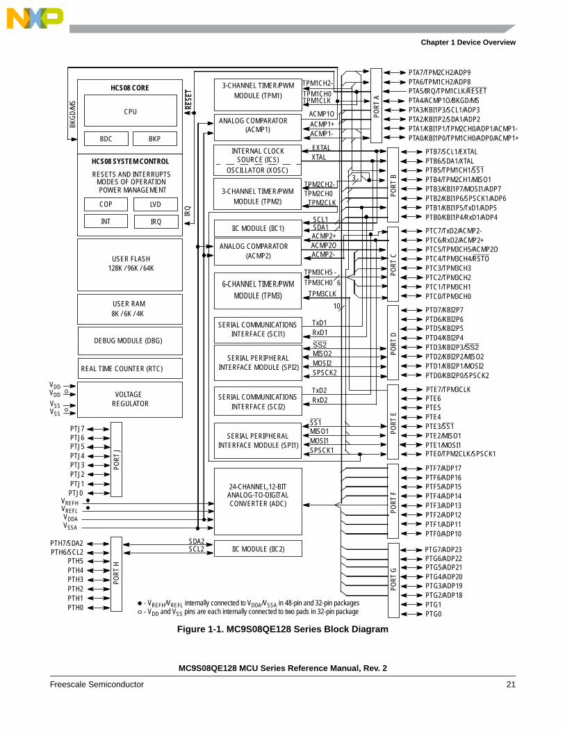
1.2 MCU Block DiagramThe block diagram in Figure 1-1 shows the structure of the MC9S08QE128 Series MCU.
MC9S08QE128 MCU Series Reference Manual, Rev. 2
20 Freescale Semiconductor
Chapter 1 Device Overview
Figure 1-1. MC9S08QE128 Series Block Diagram
TPM2CH2-TPM2CH0
TPM1CH0
TPM1CH2-
ANALOG COMPARATOR(ACMP1)
ACMP1O
ACMP1-ACMP1+
VSS
VDD
IIC MODULE (IIC1)
SERIAL PERIPHERAL INTERFACE MODULE (SPI1)
USER FLASH
USER RAM
128K / 96K / 64K
HCS08 CORE
CPU
BDC
6-CHANNEL TIMER/PWMMODULE (TPM3)
HCS08 SYSTEM CONTROL
RESETS AND INTERRUPTSMODES OF OPERATIONPOWER MANAGEMENT
VOLTAGEREGULATOR
COP
IRQ
LVD
OSCILLATOR (XOSC)
RES
ET
VREFL
VREFH
8K / 6K / 4K
BKG
D/M
S
INTERFACE (SCI1)SERIAL COMMUNICATIONS
MISO1SS1
SPSCK1
3-CHANNEL TIMER/PWMMODULE (TPM2)
REAL TIME COUNTER (RTC)
DEBUG MODULE (DBG)
IRQ
PTA3/KBI1P3/SCL1/ADP3PTA4/ACMP1O/BKGD/MSPTA5/IRQ/TPM1CLK/RESET
PTA2/KBI1P2/SDA1/ADP2PTA1/KBI1P1/TPM2CH0/ADP1/ACMP1-PTA0/KBI1P0/TPM1CH0/ADP0/ACMP1+
PORT
A
PTA6/TPM1CH2/ADP8PTA7/TPM2CH2/ADP9
MOSI1
PTB3/KBI1P7/MOSI1/ADP7PTB4/TPM2CH1/MISO1PTB5/TPM1CH1/SS1
PTB2/KBI1P6/SPSCK1/ADP6PTB1/KBI1P5/TxD1/ADP5PTB0/KBI1P4/RxD1/ADP4
PORT
B
PTB6/SDA1/XTALPTB7/SCL1/EXTAL
PTC3/TPM3CH3PTC4/TPM3CH4/RSTOPTC5/TPM3CH5/ACMP2O
PTC2/TPM3CH2PTC1/TPM3CH1PTC0/TPM3CH0
PORT
C
PTC6/RxD2/ACMP2+PTC7/TxD2/ACMP2-
PTD3/KBI2P3/SS2PTD4/KBI2P4PTD5/KBI2P5
PTD2/KBI2P2/MISO2PTD1/KBI2P1/MOSI2PTD0/KBI2P0/SPSCK2
PORT
D
PTD6/KBI2P6PTD7/KBI2P7
PTE3/SS1PTE4PTE5
PTE2/MISO1PTE1/MOSI1
TPM2CLK
PORT
EPTE6
PTE0/TPM2CLK/SPSCK1
PTF3/ADP13PTF4/ADP14PTF5/ADP15
PTF2/ADP12PTF1/ADP11PTF0/ADP10
PORT
F
PTF6/ADP16PTF7/ADP17
PTG1PTG2/ADP18PTG3/ADP19PO
RT G
PTG4/ADP20PTG5/ADP21
PTG0
VSS
VDD
VSSA
VDDA
BKP
INT
ANALOG COMPARATOR(ACMP2)
INTERFACE (SCI2)SERIAL COMMUNICATIONS
6TPM3CH5 -TPM3CH0
- VREFH/VREFL internally connected to VDDA/VSSA in 48-pin and 32-pin packages- VDD and VSS pins are each internally connected to two pads in 32-pin package
PTG6/ADP22PTG7/ADP23
SOURCE (ICS)INTERNAL CLOCK
RES
ET
PORT
JPO
RT H
PTJ1PTJ2PTJ3PTJ4PTJ5
PTJ0
PTJ6PTJ7
PTH1PTH2PTH3PTH4PTH5
PTH0
PTH6/SCL2PTH7/SDA2
IIC MODULE (IIC2)
ANALOG-TO-DIGITALCONVERTER (ADC)
24-CHANNEL,12-BIT
3-CHANNEL TIMER/PWMMODULE (TPM1)
SDA2SCL2
SERIAL PERIPHERAL INTERFACE MODULE (SPI2)
MISO2SS2
SPSCK2MOSI2
EXTALXTAL
10
SDA1SCL1
ACMP2-
ACMP2+ACMP2O
RxD1TxD1
RxD2TxD2
TPM3CLK
3
TPM1CLK
PTE7/TPM3CLK
MC9S08QE128 MCU Series Reference Manual, Rev. 2
Freescale Semiconductor 21
Chapter 1 Device Overview
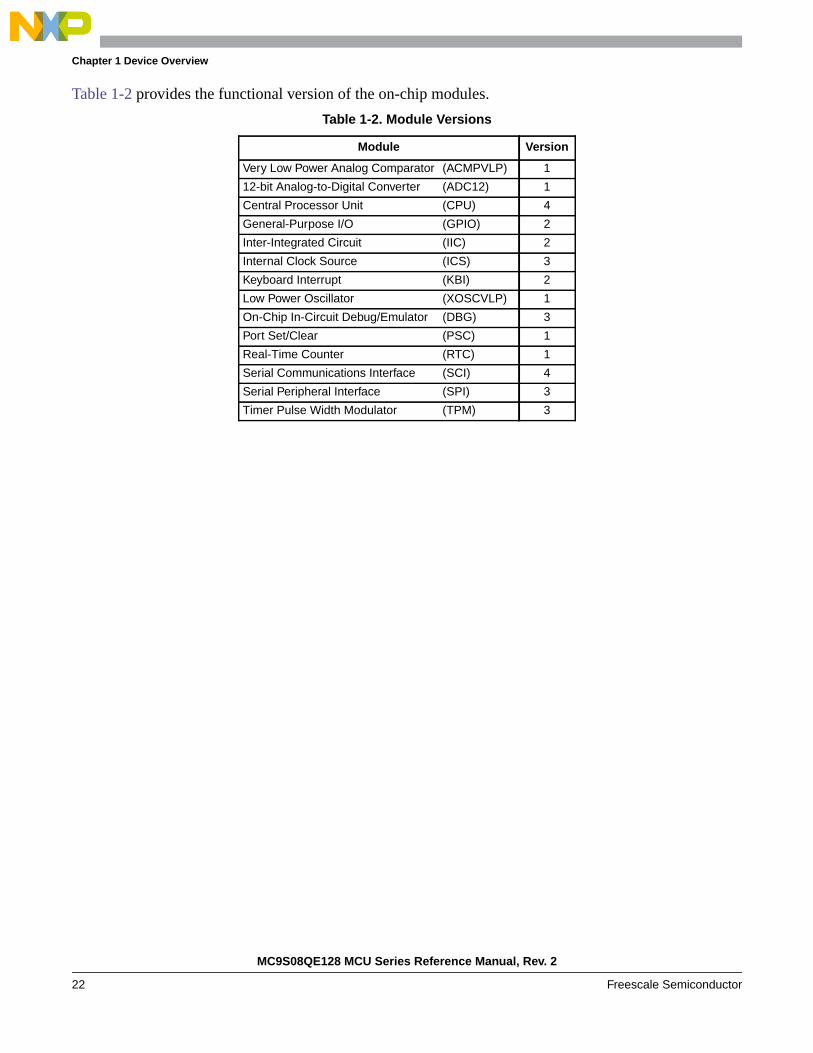
Table 1-2 provides the functional version of the on-chip modules.
Table 1-2. Module Versions
Module Version
Very Low Power Analog Comparator (ACMPVLP) 1
12-bit Analog-to-Digital Converter (ADC12) 1
Central Processor Unit (CPU) 4
General-Purpose I/O (GPIO) 2
Inter-Integrated Circuit (IIC) 2
Internal Clock Source (ICS) 3
Keyboard Interrupt (KBI) 2
Low Power Oscillator (XOSCVLP) 1
On-Chip In-Circuit Debug/Emulator (DBG) 3
Port Set/Clear (PSC) 1
Real-Time Counter (RTC) 1
Serial Communications Interface (SCI) 4
Serial Peripheral Interface (SPI) 3
Timer Pulse Width Modulator (TPM) 3
MC9S08QE128 MCU Series Reference Manual, Rev. 2
22 Freescale Semiconductor

Chapter 1 Device Overview
1.3 System Clock DistributionFigure 1-2 shows a simplified clock connection diagram. Some modules in the MCU have selectable clockinputs as shown. The clock inputs to the modules indicate the clock(s) that are used to drive the modulefunction. All memory mapped registers associated with the modules are clocked with BUSCLK. The ICSsupplies the clock sources:
• ICSOUT — This clock source is used as the CPU clock and is divided by 2 to generate theperipheral bus clock. Control bits in the ICS control registers determine which of three clocksources is connected:
— Internal reference clock
— External reference clock
— Frequency-locked loop (FLL) output
See Chapter 11, “Internal Clock Source (S08ICSV3)” for details on configuring the ICSOUTclock.
• ICSLCLK — This clock source is derived from the digitally controlled oscillator (DCO) of the ICSwhen the ICS is configured to run off of the internal or external reference clock. Development toolscan select this internal self-clocked source (~ 8 MHz) to speed up BDC communications in systemswhere the bus clock is slow. See Chapter 11, “Internal Clock Source (S08ICSV3)” for details.
• ICSERCLK — This is the external reference clock and can be selected as the alternate clock forthe ADC module. The Optional External Reference Clock section in Chapter 11, “Internal ClockSource (S08ICSV3)” explains the ICSERCLK in more detail. See Chapter 10, “Analog-to-DigitalConverter (S08ADC12V1)” for more information regarding the use of ICSERCLK with thesemodules.
• ICSIRCLK — This is the internal reference clock and can be selected as the real-time counter clocksource. The Internal Reference Clock section in Chapter 11, “Internal Clock Source (S08ICSV3)explains the ICSERCLK in more detail. See Chapter 13, “Real-Time Counter (S08RTCV1)” formore information regarding the use of ICSIRCLK.
• ICSFFCLK — This generates the fixed frequency clock (FFCLK) after being synchronized to thebus clock. It can be selected as clock source for the TPM modules. The frequency of theICSFFCLK is determined by the settings of the ICS. See the Fixed Frequency Clock section inChapter 11, “Internal Clock Source (S08ICSV3)” for details.
• LPOCLK — This clock is generated from an internal low power oscillator that is completelyindependent of the ICS module. The LPOCLK can be selected as the clock source to the RTC orCOP modules. See Chapter 13, “Real-Time Counter (S08RTCV1)” and Section 5.4, “ComputerOperating Properly (COP) Watchdog” for details on using the LPOCLK with these modules.
• OSCOUT — This is the direct output of the external oscillator module and can be selected as thereal-time counter clock source. See Chapter 13, “Real-Time Counter (S08RTCV1)” for details.
• TPMxCLK — TPMxCLKs are optional external clock sources for the TPM modules. TheTPMxCLK must be limited to 1/4th the frequency of the bus clock for synchronization. See theExternal TPM Clock Sources section in Chapter 16, “Timer/Pulse-Width Modulator (S08TPMV3)for more details.
MC9S08QE128 MCU Series Reference Manual, Rev. 2
Freescale Semiconductor 23

Chapter 1 Device Overview
E
Figure 1-2. System Clock Distribution Diagram
TPM1 TPM2 TPM3 SCI1 SCI2
BDCCPU ADC FLASH SPI2
ICS
ICSOUT ÷2BUSCLK
ICSLCLK
ICSERCLK
COP
* The fixed frequency clock (FFCLK) is internallysynchronized to the bus clock and must not exceed one halfof the bus clock frequency.
Flash has frequencyrequirements for programand erase operation. Seethe data sheet for details.
ADC has min and maxfrequency requirements.See the ADC chapterand data sheet fordetails.
XOSC
XTAL XTAL
SPI1
FFCLK*ICSFFCLK
RTC1 kHZLPO
TPM1CLK
ICSIRCLK
÷2
IIC2IIC1DBG
TPM3CLKTPM2CLK
SYNC*
LPOCLK
OSCOUT
MC9S08QE128 MCU Series Reference Manual, Rev. 2
24 Freescale Semiconductor
Chapter 2Pins and ConnectionsThis section describes signals that connect to package pins. It includes pinout diagrams, recommendedsystem connections, and detailed discussions of signals.
2.1 Device Pin AssignmentThis section shows the pin assignments for MC9S08QE128 Series devices in the available packages.
MC9S08QE128 MCU Series Reference Manual, Rev. 2
Freescale Semiconductor 25
Chapter 2 Pins and Connections
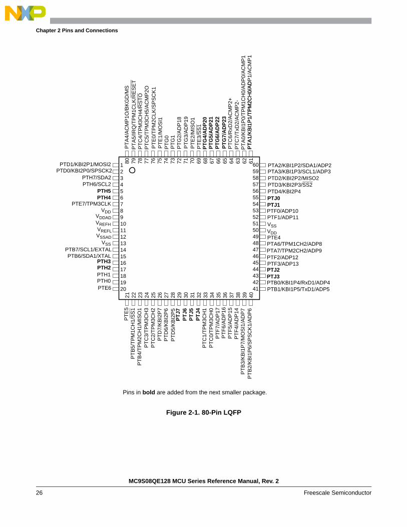
Figure 2-1. 80-Pin LQFP
1234567891011121314151617181920
80 79 78 77 76 75 74 73 72 71 70 69 68 67 66 65 64 63 62 61
21 22 23 24 25 26 27 28 29 30 31 32 33 34 35 36 37 38 39 40
6059585756555453525150494847464544434241
VREFH
VSSAD
VDD
VREFL
VDDAD
VSSPTB7/SCL1/EXTAL
PTH7/SDA2PTD0/KBI2P0/SPSCK2
PTD1/KBI2P1/MOSI2
PTE6
PTB6/SDA1/XTAL
PTH6/SCL2
PTE7/TPM3CLK
PTH1PTH0
PTH3PTH2
PTH5PTH4
PT
C2/
TP
M3C
H2
PT
B4/
TP
M2C
H1/
MIS
O1
PT
B5/
TP
M1C
H1/
SS
1
PT
C3/
TP
M3C
H3
PT
D7/
KB
I2P
7
PT
C0/
TP
M3C
H0
PT
C1/
TP
M3C
H1
PT
D6/
KB
I2P
6P
TD
5/K
BI2
P5
PT
B3/
KB
I1P
7/M
OS
I1/A
DP
7P
TB
2/K
BI1
P6/
SP
SC
K1/
AD
P6
PT
E5
PT
F7/
AD
P17
PT
F6/
AD
P16
PT
F5/
AD
P15
PT
F4/
AD
P14
PTD4/KBI2P4
VDD
VSS
PTA7/TPM2CH2/ADP9
PTB1/KBI1P5/TxD1/ADP5PTB0/KBI1P4/RxD1/ADP4
PTA2/KBI1P2/SDA1/ADP2PTA3/KBI1P3/SCL1/ADP3
PTA6/TPM1CH2/ADP8
PTD3/KBI2P3/SS2PTD2/KBI2P2/MISO2
PTE4
PTF0/ADP10PTF1/ADP11
PTF2/ADP12PTF3/ADP13
PT
E2/
MIS
O1
PT
A5/
IRQ
/TP
M1C
LK/ R
ES
ET
PT
A4/
AC
MP
1O/B
KG
D/M
S
PT
A0/
KB
I1P
0/T
PM
1CH
0/A
DP
0/A
CM
P1
PT
A1/
KB
I1P
1/T
PM
2CH
0/A
D
PT
C7/
TxD
2/A
CM
P2-
PT
C5/
TP
M3C
H5/
AC
MP
2OP
TC
4/T
PM
3CH
4/R
ST
O
PT
C6/
RxD
2/A
CM
P2+
PT
E0/
TP
M2C
LK/S
PS
CK
1P
TE
1/M
OS
I1
PT
E3/
SS
1
PT
G3/
AD
P19
PT
G2/
AD
P18
PT
G1
PT
G0
PT
G7/
AD
P23
PT
G6/
AD
P22
PT
G5/
AD
P21
PT
G4/
AD
P20
PT
J4P
TJ5
PT
J6P
TJ7
PTJ1PTJ0
PTJ3PTJ2
PT
A1/
KB
I1P
1/T
PM
2CH
0/A
DP
1/A
CM
P1
Pins in bold are added from the next smaller package.
MC9S08QE128 MCU Series Reference Manual, Rev. 2
26 Freescale Semiconductor
Chapter 2 Pins and Connections
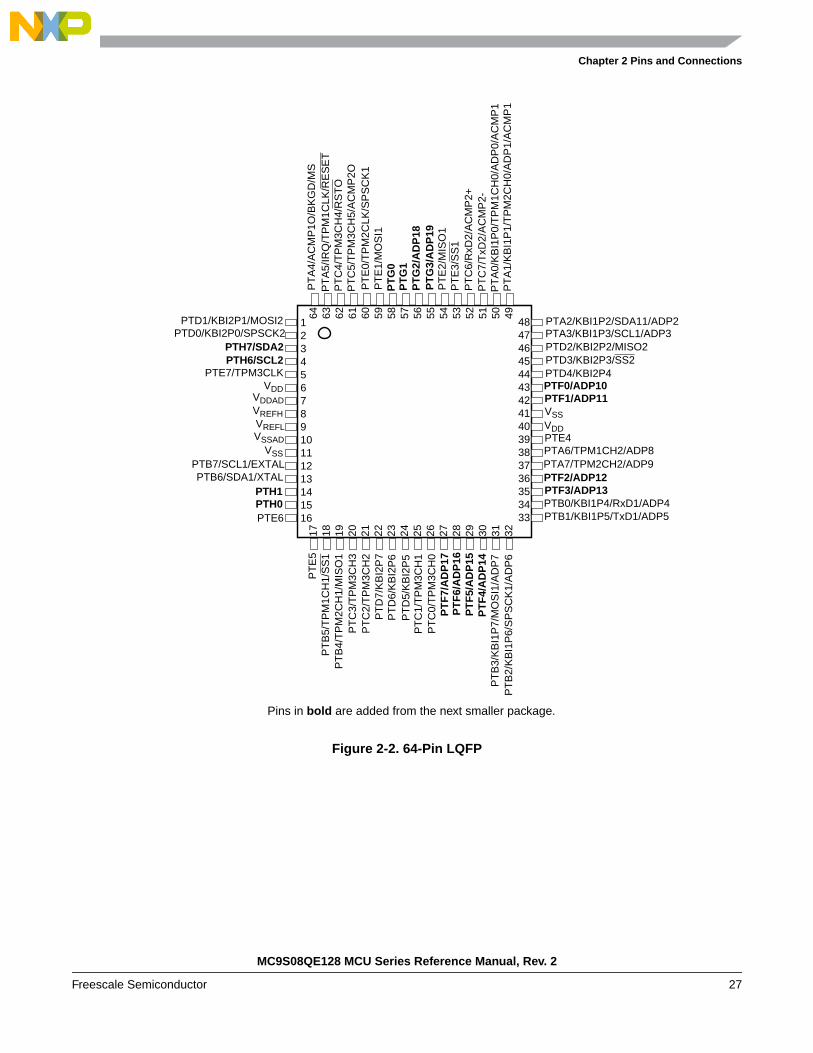
Figure 2-2. 64-Pin LQFP
12345678910111213141516
17 18 19 20 21 22 23 24 25 26 27 28 29 30 31 32
48474645444342414039383736353433
64 63 62 61 60 59 58 57 56 55 54 53 52 51 50 49
VREFH
VSSAD
VDD
VREFL
VDDAD
VSSPTB7/SCL1/EXTAL
PTH7/SDA2PTD0/KBI2P0/SPSCK2
PTD1/KBI2P1/MOSI2
PTE6
PTB6/SDA1/XTAL
PT
C2/
TP
M3C
H2
PT
B4/
TP
M2C
H1/
MIS
O1
PT
B5/
TP
M1C
H1/
SS
1
PT
C3/
TP
M3C
H3
PT
D7/
KB
I2P
7
PT
C0/
TP
M3C
H0
PT
C1/
TP
M3C
H1
PT
D6/
KB
I2P
6P
TD
5/K
BI2
P5
PT
B3/
KB
I1P
7/M
OS
I1/A
DP
7P
TB
2/K
BI1
P6/
SP
SC
K1/
AD
P6
PT
E5
PTD4/KBI2P4
VDD
VSS
PTA7/TPM2CH2/ADP9
PTB1/KBI1P5/TxD1/ADP5PTB0/KBI1P4/RxD1/ADP4
PTA2/KBI1P2/SDA11/ADP2PTA3/KBI1P3/SCL1/ADP3
PTA6/TPM1CH2/ADP8
PTD3/KBI2P3/SS2PTD2/KBI2P2/MISO2
PTE4P
TE
2/M
ISO
1
PT
A5/
IRQ
/TP
M1C
LK/R
ES
ET
PT
A4/
AC
MP
1O/B
KG
D/M
S
PT
A0/
KB
I1P
0/T
PM
1CH
0/A
DP
0/A
CM
P1
PT
A1/
KB
I1P
1/T
PM
2CH
0/A
DP
1/A
CM
P1
PT
C7/
TxD
2/A
CM
P2-
PT
C5/
TP
M3C
H5/
AC
MP
2OP
TC
4/T
PM
3CH
4/R
ST
O
PT
C6/
RxD
2/A
CM
P2+
PT
E0/
TP
M2C
LK/S
PS
CK
1P
TE
1/M
OS
I1
PT
E3/
SS
1
PTF0/ADP10PTF1/ADP11
PT
F7/
AD
P17
PT
F6/
AD
P16
PT
F5/
AD
P15
PT
F4/
AD
P14
PTF2/ADP12PTF3/ADP13
PT
G3/
AD
P19
PT
G2/
AD
P18
PT
G1
PT
G0
PTH6/SCL2PTE7/TPM3CLK
PTH1PTH0
Pins in bold are added from the next smaller package.
MC9S08QE128 MCU Series Reference Manual, Rev. 2
Freescale Semiconductor 27

Chapter 2 Pins and Connections
Figure 2-3. 48-Pin QFN
48 47 46 45 44 43 42 41 40 39
1
2
3
4
5
6
7
8
9
10
11
14 15 16 17 18 19 20 21 22
36
33
32
31
30
29
28
27
26
13 2423
25
35
34
3738
12
VREFH
VSSAD
VDD
VREFL
VDDAD
VSS
PTB7/SCL1/EXTAL
PTB6/SDA11/XTAL
PTE7/TPM3CLK
PTD0/KBI2P0/SPSCK2
PTD1/KBI2P1/MOSI2
PTE6
PT
C2/
TP
M3C
H2
PT
B4/
TP
M2C
H1/
MIS
O1
PT
B5/
TP
M1C
H1/
SS
1
PT
C3/
TP
M3C
H3
PT
D7/
KB
I2P
7
PT
C0/
TP
M3C
H0
PT
C1/
TP
M3C
H1
PT
D6/
KB
I2P
6
PT
D5/
KB
I2P
5
PT
B3/
KB
I1P
7/M
OS
I1/A
DP
7
PT
B2/
KB
I1P
6/S
PS
CK
1/A
DP
6
PT
E5
PTD4/KBI2P4
VDD
VSS
PTA7/TPM2CH2/ADP9
PTB1/KBI1P5/TxD1/ADP5
PTB0/KBI1P4/RxD1/ADP4
PTA2/KBI1P2/SDA1/ADP2
PTA3/KBI1P3/SCL1/ADP3
PTA6/TPM1CH2/ADP8
PTD3/KBI2P3/SS2
PTD2/KBI2P2/MISO2
PTE4
PT
E2/
MIS
O1
PT
A5/
IRQ
/TP
M1C
LK/R
ES
ET
PT
A4/
AC
MP
1O/B
KG
D/M
S
PT
A0/
KB
I1P
0/T
PM
1CH
0/A
DP
0/A
CM
P1
PT
A1/
KB
I1P
1/T
PM
2CH
0/A
D
PT
C7/
TxD
2/A
CM
P2-
PT
C5/
TP
M3C
H5/
AC
MP
2O
PT
C4/
TP
M3C
H4/
RS
TO
PT
C6/
RxD
2/A
CM
P2+
PT
E0/
TP
M2C
LK/S
PS
CK
1
PT
E1/
MO
SI1
PT
E3/
SS
1
PT
A1/
KB
I1P
1/T
PM
2CH
0/A
DP
1/A
CM
P1
Pins in bold are added from the next smaller package.
MC9S08QE128 MCU Series Reference Manual, Rev. 2
28 Freescale Semiconductor
Chapter 2 Pins and Connections
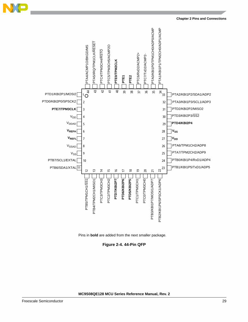
Figure 2-4. 44-Pin QFP
44 3443 42 41 40 39 38 37 36 35
1
2
3
4
5
6
7
8
9
10
11
13 14 15 16 17 18 19 20 21
33
32
31
30
29
28
27
26
25
24
12 22
23
VREFH
VSSAD
VDD
VREFL
VDDAD
PT
E2
PTD4/KBI2P4
VSS
PT
C2/
TP
M3C
H2
PT
B4/
TP
M2C
H1/
MIS
O1
PTB7/SCL1/EXTAL
PTB6/SDA1/XTAL
PT
B5/
TP
M1C
H1/
SS
1
PT
C3/
TP
M3C
H3
PT
A5/
IRQ
/TP
M1C
LK/ R
ES
ET
PT
A4/
AC
MP
1O/B
KG
D/M
S
PT
D7/
KB
I2P
7
PT
C0/
TP
M3C
H0
PT
C1/
TP
M3C
H1
VDD
VSS
PT
D6/
KB
I2P
6
PT
D5/
KB
I2P
5
PT
A0/
KB
I1P
0/T
PM
1CH
0/A
DP
0/A
CM
P1
PT
A1/
KB
I1P
1/T
PM
2CH
0/A
DP
1/A
CM
P1
PT
C7/
TxD
2/A
CM
P2-
PT
C5/
TP
M3C
H5/
AC
MP
2O
PT
C4/
TP
M3C
H4/
RS
TO
PT
C6/
RxD
2/A
CM
P2+
PTA7/TPM2CH2/ADP9P
TB
3/K
BI1
P7/
MO
SI1
/AD
P7
PT
B2/
KB
I1P
6/S
PS
CK
1/A
DP
6
PTB1/KBI1P5/TxD1/ADP5
PTB0/KBI1P4/RxD1/ADP4
PTA2/KBI1P2/SDA1/ADP2
PTA3/KBI1P3/SCL1/ADP3
PTA6/TPM1CH2/ADP8
PT
E0/
TP
M2C
LK
PT
E1
PTE7/TPM3CLK
PTD0/KBI2P0/SPSCK2
PTD1/KBI2P1/MOSI2
PTD3/KBI2P3/SS2
PTD2/KBI2P2/MISO2
Pins in bold are added from the next smaller package.
MC9S08QE128 MCU Series Reference Manual, Rev. 2
Freescale Semiconductor 29
Chapter 2 Pins and Connections
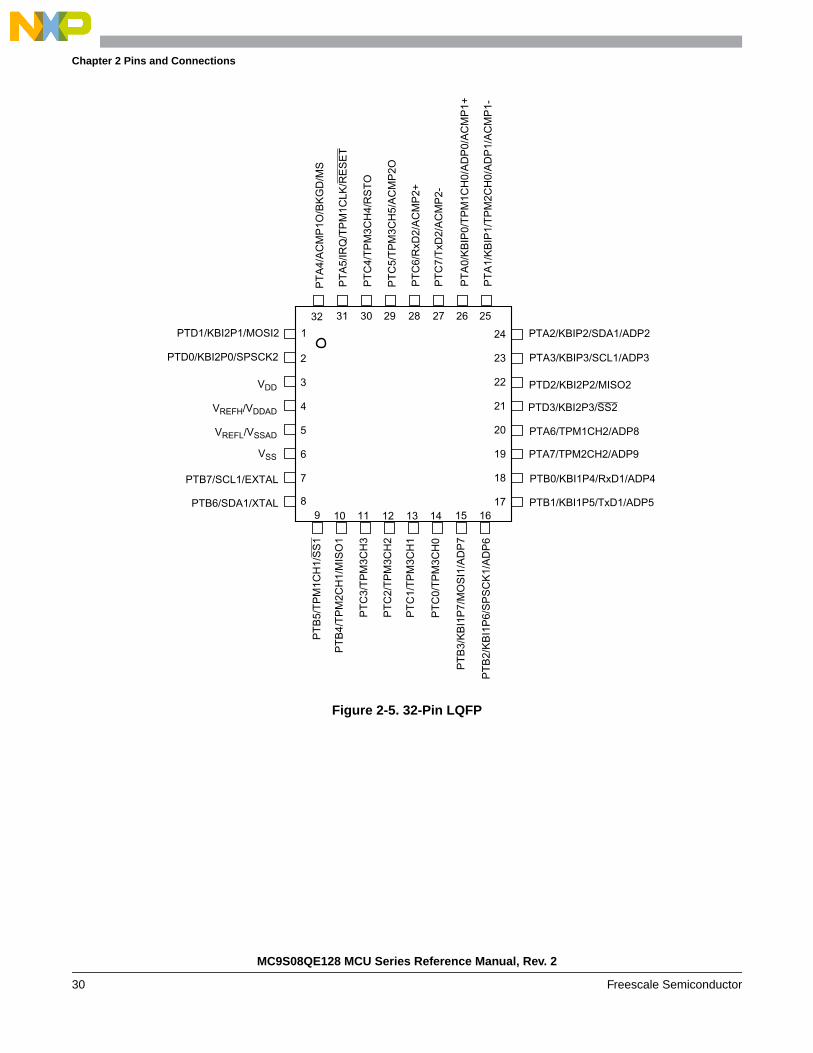
Figure 2-5. 32-Pin LQFP
PTD3/KBI2P3/SS2VREFH/VDDAD
1
2
3
4
5
6
7
8
VREFL/VSSAD
VSS 19
18
1710 11 12 13 14 159
24
32
16
252627
VDD
20
21
22
23
31 30 29 28
PT
A5/
IRQ
/TP
M1C
LK/R
ES
ET
PT
A4/
AC
MP
1O/B
KG
D/M
S
PTA7/TPM2CH2/ADP9P
TA
0/K
BIP
0/T
PM
1CH
0/A
DP
0/A
CM
P1+
PT
C0/
TP
M3C
H0
PT
B3/
KB
I1P
7/M
OS
I1/A
DP
7
PT
B2/
KB
I1P
6/S
PS
CK
1/A
DP
6
PTB1/KBI1P5/TxD1/ADP5
PTB0/KBI1P4/RxD1/ADP4
PTA2/KBIP2/SDA1/ADP2
PTA3/KBIP3/SCL1/ADP3
PT
A1/
KB
IP1/
TP
M2C
H0/
AD
P1/
AC
MP
1-
PT
C1/
TP
M3C
H1
PT
C2/
TP
M3C
H2
PT
B4/
TP
M2C
H1/
MIS
O1
PT
C7/
TxD
2/A
CM
P2-
PTB6/SDA1/XTAL
PT
B5/
TP
M1C
H1/
SS
1
PT
C5/
TP
M3C
H5/
AC
MP
2O
PT
C4/
TP
M3C
H4/
RS
TO
PT
C3/
TP
M3C
H3
PTD0/KBI2P0/SPSCK2
PTD1/KBI2P1/MOSI2
PTB7/SCL1/EXTAL
PTD2/KBI2P2/MISO2
PTA6/TPM1CH2/ADP8
PT
C6/
RxD
2/A
CM
P2+
MC9S08QE128 MCU Series Reference Manual, Rev. 2
30 Freescale Semiconductor

Chapter 2 Pins and Connections
2.2 Recommended System ConnectionsFigure 2-6 shows pin connections that are common to MC9S08QE128 Series application systems.
MC9S08QE128 MCU Series Reference Manual, Rev. 2
Freescale Semiconductor 31

Chapter 2 Pins and Connections
Figure 2-6. Basic System Connections
VDD
VSS
BKGD/MS
RESET/IRQ
OPTIONALMANUALRESET
PORTA
VDD
BACKGROUND HEADER
C2C1 X1
RF RS
CBY0.1 μF
SYSTEMPOWER
PTA0/KBI1P0/TPM1CH0/ADP0/ACMP1+PTA1/KBI1P1/TPM2CH0/ADP1/ACMP1-PTA2/KBI1P2/SDA1/ADP2PTA3/KBI1P3/SCL1/ADP3PTA4/ACMP1O/BKGD/MSPTA5/IRQ/TCLK1/RESETPTA6/TPM1CH2/ADP8PTA7/TPM2CH2/ADP9
PORTB
PTB0/KBI1P4/RxD1/ADP4PTB1/KBI1P5/TxD1/ADP5PTB2/KBI1P6/SPSCK1/ADP6PTB3/KBI1P7/MOSI1/ADP7PTB4/TPM2CH1/MISO1PTB5/TPM1CH1/SS1PTB6/SDA1/XTALPTB7/SCL1/EXTAL
PORTC
PTC0/TPM3CH0PTC1/TPM3CH1PTC2/TPM3CH2PTC3/TPM3CH3PTC4/TPM3CH4/RSTOPTC5/TPM3CH5/ACMP2OPTC6/RxD2/ACMP2+
D
PTD0/KBI2P0/SPSCK2PTD1/KBI2P1/MOSI2PTD2/KBI2P2/MISO2PTD3/KBI2P3/SS2PTD4/KBI2P4PTD5/KBI2P5PTD6/KBI2P6PTD7/KBI2P7
PORTE
PTE0/TCLK2/SPSCK1PTE1/MOSI1PTE2/MISO1PTE3/SS1PTE4PTE5PTE6PTE7/TPM3CLK
PORT
H
PTH0PTH1PTH2PTH3PTH4PTH5
PTH6/SCL2PTH7/SDA2
MC9S08QE128
VREFH
VREFL
CBYAD0.1 μF
VSSA
VDDA
PTC7/TxD2/ACMP2-
VDD
VSS
CBY0.1 μF
CBLK10 μF
+3 V
+
PORT
PTF0/ADP10PTF1/ADP11PTF2/ADP12PTF3/ADP13PTF4/ADP14PTF5/ADP15PTF6/ADP16PTF7/ADP17
PORTF
PTG0PTG1PTG2/ADP18PTG3/ADP19PTG4/ADP20PTG5/ADP21PTG6/ADP22PTG7/ADP23
PORTG
PORT
J
PTJ0PTJ1PTJ2PTJ3PTJ4PTJ5PTJ6PTJ7
OPTIONAL EXTERNAL OSCILLATOR
OPTIONALEMC
PROTECTION
VDD
4.7 kΩ–10 kΩ
0.1 μF
XTAL
EXTAL
NOTES:1. RESET pin can only
be used to reset intouser mode, you cannot enter BDM usingRESET pin. BDMcan be entered byholding MS lowduring POR orwriting a 1 to BDFRin SBDFR with MSlow after issuingBDM command.
2. RESET/IRQfeatureshave optionalinternal pullupdevice.
3. RC filter onRESET/IRQ pinrecommended fornoisy environments.
4. C1, C2, RF, and RSare not requiredwhen low range lowpower oscillator isselected.
(NOTE 3)
(NOTE 1)
(NOTE 2)
(NOTE 4)
MC9S08QE128 MCU Series Reference Manual, Rev. 2
32 Freescale Semiconductor
Chapter 2 Pins and Connections
2.2.1 Power
VDD and VSS are the primary power supply pins for the MCU. This voltage source supplies power to allI/O buffer circuitry and to an internal voltage regulator. The internal voltage regulator provides regulatedlower-voltage source to the CPU and other internal circuitry of the MCU.
Typically, application systems have two separate capacitors across the power pins. In this case, thereshould be a bulk electrolytic capacitor, such as a 10-μF tantalum capacitor, to provide bulk charge storagefor the overall system and a 0.1-μF ceramic bypass capacitor located as near to the MCU power pins aspractical to suppress high-frequency noise. Actual decoupling capacitor values and number will varyaccording to layout and application. The MC9S08QE128 Series has two VDD pins except on the 32-pinpackage. Each pin must have a bypass capacitor for best noise suppression.
VDDA and VSSA are the analog power supply pins for the MCU. This voltage source supplies power to theADC module. A 0.1-μF ceramic bypass capacitor should be located as near to the MCU power pins aspractical to suppress high-frequency noise.
2.2.2 Oscillator
Immediately after reset, the MCU uses an internally generated clock provided by the internal clock source(ICS) module. For more information on the ICS, see Chapter 11, “Internal Clock Source (S08ICSV3).”
The oscillator (XOSCVLP) in this MCU is a Pierce oscillator that can accommodate a crystal or ceramicresonator. Optionally, an external clock source can be connected to the EXTAL input pin. The oscillatorcan be configured to run in stop2 or stop3 modes.
Refer to Figure 2-6 for the following discussion. RS (when used) and RF should be low-inductanceresistors such as carbon composition resistors. Wire-wound resistors, and some metal film resistors, havetoo much inductance. C1 and C2 normally should be high-quality ceramic capacitors that are specificallydesigned for high-frequency applications.
RF is used to provide a bias path to keep the EXTAL input in its linear range during crystal startup; its valueis not generally critical. Typical systems use 1 MΩ to 10 MΩ. Higher values are sensitive to humidity andlower values reduce gain and (in extreme cases) could prevent startup.
C1 and C2 are typically in the 5-pF to 25-pF range and are chosen to match the requirements of a specificcrystal or resonator. Be sure to take into account printed circuit board (PCB) capacitance and MCU pincapacitance when selecting C1 and C2. The crystal manufacturer typically specifies a load capacitancewhich is the series combination of C1 and C2 (which are usually the same size). As a first-orderapproximation, use 10 pF as an estimate of combined pin and PCB capacitance for each oscillator pin(EXTAL and XTAL).
When using the oscillator in low range and low gain mode, the external components RS, RF, C1 and C2 arenot required.
2.2.3 RESET and RSTO
After a power-on reset (POR), the PTA5/IRQ/TCLK/RESET pin defaults to a general-purpose input portpin, PTA5. Setting RSTPE in SOPT1 configures the pin to be the RESET pin. After configured as RESET,
MC9S08QE128 MCU Series Reference Manual, Rev. 2
Freescale Semiconductor 33

Chapter 2 Pins and Connections
the pin will remain RESET until the next POR. The RESET pin can be used to reset the MCU from anexternal source when the pin is driven low. When enabled as the RESET pin (RSTPE = 1), the pin isconfigured as an input only with an internal pullup device automatically enabled.
NOTEThis pin does not contain a clamp diode to VDD and should not be drivenabove VDD.
NOTEThe RESET pin is pulled to VDD internally. The external voltage measuredon the RESET pin will be less than VDD. Therefore, the RESET pullupshould not be used to pullup components external to the MCU.
NOTEIn EMC-sensitive applications, an external RC filter is recommended on theRESET pin, if enabled. See Figure 2-6 for an example.
After a power-on reset (POR), the PTC4/TPM3CH4/RSTO pin defaults to a general-purpose port pin,PTC4. Setting RSTOPE in SOPT1 configures the pin to be the RSTO pin. After configured as RSTO, thepin will remain RSTO until the next POR. The RSTO pin will reflect the current state of the internal MCUreset signal. As long as the MCU is not in a reset state, the RSTO pin will drive high. Whenever the MCUis in a reset state, this pin will drive low until the internal reset signal is released. When enabled as theRSTO pin (RSTOPE = 1), the pin is automatically configured as an output only. The RSTO pin can beenabled independently of the RESET pin.
2.2.4 Background / Mode Select (BKGD/MS)
During a power-on-reset (POR) or background debug force reset (see Section 5.8.3, “System BackgroundDebug Force Reset Register (SBDFR),” for more information), the PTA4/ACMPO/BKGD/MS pinfunctions as a mode select pin. Immediately after any reset, the pin functions as the background pin andcan be used for background debug communication. When enabled as the BKGD/MS pin (BKGDPE = 1),an internal pullup device is automatically enabled.
The background debug communication function is enabled when BKGDPE in SOPT1 is set. BKGDPE isset following any reset of the MCU and must be cleared to use the PTA4/ACMPO/BKGD/MS pin’salternative pin functions.
If nothing is connected to this pin, the MCU will enter normal operating mode at the rising edge of theinternal reset after a POR or force BDC reset. If a debug system is connected to the 6-pin standardbackground debug header, it can hold BKGD/MS low during a POR or immediately after issuing a back-ground debug force reset, which will force the MCU to active background mode.
The BKGD/MS pin is used primarily for background debug controller (BDC) communications using acustom protocol that uses 16 clock cycles of the target MCU’s BDC clock per bit time. The target MCU’sBDC clock could be as fast as the bus clock rate, so there should never be any significant capacitanceconnected to the BKGD/MS pin that could interfere with background serial communications.
MC9S08QE128 MCU Series Reference Manual, Rev. 2
34 Freescale Semiconductor

Chapter 2 Pins and Connections
Although the BKGD/MS pin is a pseudo open-drain pin, the background debug communication protocolprovides brief, actively driven, high speedup pulses to ensure fast rise times. Small capacitances fromcables and the absolute value of the internal pull-up device play almost no role in determining rise and falltimes on the BKGD/MS pin.
2.2.5 ADC Reference Pins (VREFH, VREFL)
The VREFH and VREFL pins are the voltage reference high and voltage reference low inputs, respectively,for the ADC module. In the 32-pin package, VREFH and VREFL are shared with VDDA and VSSA,respectively.
2.2.6 General-Purpose I/O and Peripheral Ports
The MC9S08QE128 Series of MCUs support up to 70 general-purpose I/O pins 1 input-only pin, and 1output-only pin, which are shared with on-chip peripheral functions (timers, serial I/O, ADC, ACMP, etc.).
When a port pin is configured as a general-purpose output or a peripheral uses the port pin as an output,software can select one of two drive strengths and enable or disable slew rate control. When a port pin isconfigured as a general-purpose input or a peripheral uses the port pin as an input, software can enable apull-up device. Immediately after reset, all of these pins are configured as high-impedance general-purposeinputs with internal pull-up devices disabled.
PTA5 is a special-case input pin. When the PTA5/IRQ/TCLK/RESET pin is configured as PTA5 with thepullup enabled, the voltage observed on the pin will not be pulled to VDD. However, the internal voltageon the PTA5 node will be at VDD.
When an on-chip peripheral system is controlling a pin, data direction control bits still determine what isread from port data registers even though the peripheral module controls the pin direction by controllingthe enable for the pin’s output buffer. For information about controlling these pins as general-purpose I/Opins, see Chapter 6, “Parallel Input/Output Control.”
NOTETo avoid extra current drain from floating input pins, the reset initializationroutine in the application program should either enable on-chip pull-updevices or change the direction of unused or non-bonded pins to outputs sothey do not float.
MC9S08QE128 MCU Series Reference Manual, Rev. 2
Freescale Semiconductor 35
Chapter 2 Pins and Connections
Table 2-1. Pin Assignment by Package and Pin Sharing Priority
Pin Number <-- Lowest Priority --> Highest
80 64 48 44 32 Port Pin Alt 1 Alt 2 Alt 3 Alt 4
1 1 1 1 1 PTD1 KBI2P1 MOSI2
2 2 2 2 2 PTD0 KBI2P0 SPSCK2
3 3 — — — PTH7 SDA2
4 4 — — — PTH6 SCL2
5 — — — — PTH5
6 — — — — PTH4
7 5 3 3 — PTE7 TPM3CLK
8 6 4 4 3 VDD
9 7 5 54
VDDA
10 8 6 6 VREFH
11 9 7 75
VREFL
12 10 8 8 VSSA
13 11 9 9 6 VSS
14 12 10 10 7 PTB7 SCL11 EXTAL
15 13 11 11 8 PTB6 SDA11 XTAL
16 — — — — PTH3
17 — — — — PTH2
18 14 — — — PTH1
19 15 — — — PTH0
20 16 12 — — PTE6
21 17 13 — — PTE5
22 18 14 12 9 PTB5 TPM1CH1 SS12
23 19 15 13 10 PTB4 TPM2CH1 MISO12
24 20 16 14 11 PTC3 TPM3CH3
25 21 17 15 12 PTC2 TPM3CH2
26 22 18 16 — PTD7 KBI2P7
27 23 19 17 — PTD6 KBI2P6
28 24 20 18 — PTD5 KBI2P5
29 — — — — PTJ7
30 — — — — PTJ6
31 — — — — PTJ5
32 — — — — PTJ4
33 25 21 19 13 PTC1 TPM3CH1
34 26 22 20 14 PTC0 TPM3CH0
35 27 — — — PTF7 ADP17
36 28 — — — PTF6 ADP16
37 29 — — — PTF5 ADP15
38 30 — — — PTF4 ADP14
39 31 23 21 15 PTB3 KBI1P7 MOSI12 ADP7
40 32 24 22 16 PTB2 KBI1P6 SPSCK12 ADP6
MC9S08QE128 MCU Series Reference Manual, Rev. 2
36 Freescale Semiconductor

Chapter 2 Pins and Connections
41 33 25 23 17 PTB1 KBI1P5 TxD1 ADP5
42 34 26 24 18 PTB0 KBI1P4 RxD1 ADP4
43 — — — — PTJ3
44 — — — — PTJ2
45 35 — — — PTF3 ADP13
46 36 — — — PTF2 ADP12
47 37 27 25 19 PTA7 TPM2CH2 ADP9
48 38 28 26 20 PTA6 TPM1CH2 ADP8
49 39 29 — — PTE4
50 40 30 27 — VDD
51 41 31 28 — VSS
52 42 — — — PTF1 ADP11
53 43 — — — PTF0 ADP10
54 — — — — PTJ1
55 — — — — PTJ0
56 44 32 29 — PTD4 KBI2P4
57 45 33 30 21 PTD3 KBI2P3 SS2
58 46 34 31 22 PTD2 KBI2P2 MISO2
59 47 35 32 23 PTA3 KBI1P3 SCL11 ADP3
60 48 36 33 24 PTA2 KBI1P2 SDA11 ADP2
61 49 37 34 25 PTA1 KBI1P1 TPM2CH0 ADP13 ACMP1-3
62 50 38 35 26 PTA0 KBI1P0 TPM1CH0 ADP03 ACMP1+3
63 51 39 36 27 PTC7 TxD2 ACMP2-
64 52 40 37 28 PTC6 RxD2 ACMP2+
65 — — — — PTG7 ADP23
66 — — — — PTG6 ADP22
67 — — — — PTG5 ADP21
68 — — — — PTG4 ADP20
69 53 41 — — PTE3 SS12
70 54 42 38 — PTE2 MISO12
71 55 — — — PTG3 ADP19
72 56 — — — PTG2 ADP18
73 57 — — — PTG1
74 58 — — — PTG0
75 59 43 39 — PTE1 MOSI12
76 60 44 40 — PTE0 TPM2CLK SPSCK12
77 61 45 41 29 PTC5 TPM3CH5 ACMP2O
78 62 46 42 30 PTC4 TPM3CH4 RSTO
79 63 47 43 31 PTA5 IRQ TPM1CLK RESET
80 64 48 44 32 PTA4 ACMP1O BKGD MS
Table 2-1. Pin Assignment by Package and Pin Sharing Priority (continued)
Pin Number <-- Lowest Priority --> Highest
80 64 48 44 32 Port Pin Alt 1 Alt 2 Alt 3 Alt 4
MC9S08QE128 MCU Series Reference Manual, Rev. 2
Freescale Semiconductor 37

Chapter 2 Pins and Connections
1 IIC1 pins (SCL1 and SDA1) can be repositioned using IIC1PS in SOPT2. Default locations arePTA3 and PTA, respectively.
2 SPI1 pins (SS1, MISO1, MOSI1, and SPSCK1) can be repositioned using SPI1PS in SOPT2.Default locations are PTB5, PTB4, PTB3, and PTB2.
3 If ADC and ACMP1 are enabled, both modules will have access to the pin.
MC9S08QE128 MCU Series Reference Manual, Rev. 2
38 Freescale Semiconductor

Chapter 3Modes of Operation
3.1 IntroductionThe operating modes of the MC9S08QE128 Series are described in this chapter. Entry into each mode,exit from each mode, and functionality while in each of the modes are described.
3.2 Features• Active background mode for code development
• Run mode — CPU clocks can be run at full speed and the internal supply is fully regulated.
• LPRUN mode — CPU clocks are restricted to a maximum of 250 kHz, peripheral clocks arerestricted to a maximum of 125 kHz, and the internal voltage regulator is in standby
• Wait mode — CPU shuts down to conserve power; system clocks are running and full regulationis maintained
• LPWAIT mode — CPU shuts down to conserve power; peripheral clocks are restricted to 125 kHzmaximum and the internal voltage regulator is in standby
• Stop modes — System clocks are stopped and voltage regulator is in standby
— Stop3 — All internal circuits are powered for fast recovery
— Stop2 — Partial power down of internal circuits, RAM content is retained; I/O states are held
3.3 Run ModeThis is the normal operating mode for the MC9S08QE128 Series. In this mode, the CPU executes codefrom internal memory with execution beginning at the address fetched from memory at 0xFFFE–0xFFFFafter reset.
3.3.1 Low Power Run Mode (LPRun)
In the low power run mode, the on-chip voltage regulator is put into its standby state. In this state, thepower consumption is reduced to a minimum that still allows CPU functionality. Power consumption isreduced the most by disabling the clocks to all unused peripherals by clearing the corresponding bits in theSCGC1 and SCGC2 registers.
Before entering this mode, the following conditions must be met:
• FBELP is the selected clock mode for the ICS (See the FBELP section in Chapter 11, “InternalClock Source (S08ICSV3).”
• The HGO bit in the ICSC2 register is clear.
MC9S08QE128 MCU Series Reference Manual, Rev. 2
Freescale Semiconductor 39
Chapter 3 Modes of Operation
• The bus frequency is 125 kHz or less.
• The ADC if enabled must be configured to use the asynchronous clock source, ADACK, to meetthe ADC minimum frequency requirements. The bandgap channel cannot be converted in lowpower run mode.
• The LVDE or LVDSE bit in SPMSC1 register must be clear. LVD and LVW will automatically bedisabled.
• Flash programming/erasing is not allowed.
• ACMP option to compare to internal bandgap reference is not allowed.
• The MCU cannot be in active background mode.
Once these conditions are met, low power run mode can be entered by setting the LPR bit in the SPMSC2register.
To re-enter standard run mode, simply clear the LPR bit. The LPRS bit in the SPMSC2 register is aread-only status bit that can be used to determine if the regulator is in full regulation mode or not. WhenLPRS is ‘0’, the regulator is in full regulation mode and the MCU can run at full speed in any clock mode.
3.3.1.1 Interrupts in Low Power Run Mode
Low power run mode provides the option to return to full regulation if any interrupt occurs. This is doneby setting the LPWUI bit in the SPMSC2 register. The ICS can then be set for full speed immediately inthe interrupt service routine.
If the LPWUI bit is clear, interrupts will be serviced in low power run mode.
If the LPWUI bit is set, LPR and LPRS bits will be cleared and interrupts will be serviced with theregulator in full regulation.
3.3.1.2 Resets in Low Power Run Mode
Any reset will exit low power run mode, clear the LPR and LPRS bits and return the device to normal runmode.
3.3.1.3 BDM in Low Power Run Mode
Low power run mode cannot be entered when the MCU is in active background debug mode.
If a device is in low power run mode, a falling edge on an active BKGD/MS pin exits low power run mode,clears the LPR and LPRS bits, and returns the device to normal run mode.
3.3.1.4 BDM in Low Power Wait Mode
If a device is in low power wait mode, a falling edge on an active BKGD/MS pin exits low power waitmode, clears the LPR and LPRS bits, and returns the device to normal run mode.
MC9S08QE128 MCU Series Reference Manual, Rev. 2
40 Freescale Semiconductor

Chapter 3 Modes of Operation
3.4 Active Background ModeThe active background mode functions are managed through the background debug controller (BDC) inthe HCS08 core. The BDC, together with the on-chip debug module (DBG), provide the means foranalyzing MCU operation during software development.
Active background mode is entered in any of six ways:
• When the BKGD/MS pin is low during POR
• When the BKGD/MS pin is low immediately after issuing a background debug force reset (seeSection 5.8.3, “System Background Debug Force Reset Register (SBDFR)”)
• When a BACKGROUND command is received through the BKGD/MS pin
• When a BGND instruction is executed
• When encountering a BDC breakpoint
• When encountering a DBG breakpoint
After entering active background mode, the CPU is held in a suspended state waiting for serial backgroundcommands rather than executing instructions from the user application program.
Background commands are of two types:
• Non-intrusive commands, defined as commands that can be issued while the user program isrunning. Non-intrusive commands can be issued through the BKGD pin while the MCU is in runmode; non-intrusive commands can also be executed when the MCU is in the active backgroundmode. Non-intrusive commands include:
— Memory access commands
— Memory-access-with-status commands
— BDC register access commands
— The BACKGROUND command
• Active background commands, which can only be executed while the MCU is in active backgroundmode. Active background commands include commands to:
— Read or write CPU registers
— Trace one user program instruction at a time
— Leave active background mode to return to the user application program (GO)
The active background mode is used to program a bootloader or user application program into the flashprogram memory before the MCU is operated in run mode for the first time. When the MC9S08QE128Series is shipped from the Freescale Semiconductor factory, the flash program memory is erased by defaultunless specifically noted, so there is no program that could be executed in run mode until the flash memoryis initially programmed. The active background mode can also be used to erase and reprogram the flashmemory after it has been previously programmed.
For additional information about the active background mode, refer to the Development Support chapter.
MC9S08QE128 MCU Series Reference Manual, Rev. 2
Freescale Semiconductor 41

Chapter 3 Modes of Operation
3.5 Wait ModeWait mode is entered by executing a WAIT instruction. Upon execution of the WAIT instruction, the CPUenters a low-power state in which it is not clocked. The I bit in CCR is cleared when the CPU enters thewait mode, enabling interrupts. When an interrupt request occurs, the CPU exits the wait mode andresumes processing, beginning with the stacking operations leading to the interrupt service routine.
While the MCU is in wait mode, there are some restrictions on which background debug commands canbe used. Only the BACKGROUND command and memory-access-with-status commands are availablewhen the MCU is in wait mode. The memory-access-with-status commands do not allow memory access,but they report an error indicating that the MCU is in either stop or wait mode. The BACKGROUNDcommand can be used to wake the MCU from wait mode and enter active background mode.
3.5.1 Low Power Wait Mode (LPWait)
Low power wait mode is entered by executing a WAIT instruction while the MCU is in low power runmode. In the low power wait mode, the on-chip voltage regulator remains in its standby state as in the lowpower run mode. In this state, the power consumption is reduced to a minimum that still allows mostmodules to maintain functionality. Power consumption is reduced the most by disabling the clocks to allunused peripherals by clearing the corresponding bits in the SCGC register.
The same restrictions from the low power run mode apply to low power wait mode.
3.5.1.1 Interrupts in Low Power Wait Mode
If the LPWUI bit is set when the WAIT instruction is executed, then the voltage regulator will return to fullregulation when wait mode is exited. The ICS can be set for full speed immediately in the interrupt serviceroutine.
If the LPWUI bit is clear when the WAIT instruction is executed, an interrupt will return the device to lowpower run mode.
If the LPWUI bit is set when the WAIT instruction is executed, an interrupt will return the device to normalrun mode with full regulation and the LPR and LPRS bits will be cleared.
3.5.1.2 Resets in Low Power Wait Mode
Any reset will exit low power wait mode, clear LPR and LPRS bit, and return the device to normal runmode.
3.6 Stop ModesEither stop2 or stop3 is entered upon execution of a STOP instruction when the STOPE bit in the systemoption 1 register (SOPT1) is set. In both stop modes, the bus and CPU clocks are halted. In stop3 theregulator is in standby. In stop2 the regulator is in partial powerdown. The ICS module can be configuredto leave the reference clocks running. See Chapter 11, “Internal Clock Source (S08ICSV3)” for moreinformation.
MC9S08QE128 MCU Series Reference Manual, Rev. 2
42 Freescale Semiconductor
Chapter 3 Modes of Operation
If the STOPE bit is not set when the CPU executes a STOP instruction, the MCU will not enter either ofthe stop modes and an illegal opcode reset is forced. The stop modes are selected by setting the appropriatebits in the Section 5.8.10, “System Clock Gating Control 1 Register (SCGC1).”
Table 3-1 shows all of the control bits that affect stop mode selection and the mode selected under variousconditions. The selected mode is entered following the execution of a STOP instruction.
3.6.1 Stop2 Mode
3.6.1.1 Stop2 Entry
Stop2 mode is entered by executing a STOP instruction under the conditions as shown in Table 3-1.
3.6.1.2 Behavior in Stop2
Most of the internal circuitry of the MCU is powered off in stop2 with the exception of the RAM andoptionally the RTC and low power oscillator (LPO), and the low-range low-gain oscillator (XOSCVLP).Upon entering stop2, all I/O pin control signals are latched so that the pins retain their states during stop2.
3.6.1.3 Exit from Stop2
Exit from stop2 is performed by asserting the wake-up pin (PTA5/IRQ/TCLK/RESET) on the MCU.
NOTEPTA5/IRQ/TPM1CLK/RESET functions as an active-low wakeup inputwhen the MCU is in stop2. The pullup on this pin is not automaticallyenabled in stop2. To enable the internal pullup, set the PTAPE5 bit in theport A pull enable register (PTAPE).
Table 3-1. Stop Mode Selection
Register SOPT1 BDCSCR SPMSC1 SPMSC2
Stop ModeBit
nameSTOPE ENBDM 1
1 ENBDM is located in the BDCSCR, which is only accessible through BDC commands; see the “BDC Status and ControlRegister (BDCSCR)” section in Chapter 17, “Development Support.”
LVDE LVDSE PPDC
0 x x x Stop modes disabled; illegal opcode reset if STOPinstruction executed
1 1 x x Stop3 with BDM enabled 2
2 When in Stop3 mode with BDM enabled, The SIDD will be near RIDD levels because internal clocks are enabled.
1 0 Both bits must be 1 x Stop3 with voltage regulator active
1 0 Either bit a 0 0 Stop3
1 0 Either bit a 0 1 Stop2
MC9S08QE128 MCU Series Reference Manual, Rev. 2
Freescale Semiconductor 43
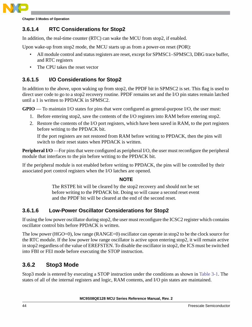
Chapter 3 Modes of Operation
3.6.1.4 RTC Considerations for Stop2
In addition, the real-time counter (RTC) can wake the MCU from stop2, if enabled.
Upon wake-up from stop2 mode, the MCU starts up as from a power-on reset (POR):
• All module control and status registers are reset, except for SPMSC1–SPMSC3, DBG trace buffer,and RTC registers
• The CPU takes the reset vector
3.6.1.5 I/O Considerations for Stop2
In addition to the above, upon waking up from stop2, the PPDF bit in SPMSC2 is set. This flag is used todirect user code to go to a stop2 recovery routine. PPDF remains set and the I/O pin states remain latcheduntil a 1 is written to PPDACK in SPMSC2.
GPIO — To maintain I/O states for pins that were configured as general-purpose I/O, the user must:
1. Before entering stop2, save the contents of the I/O registers into RAM before entering stop2.
2. Restore the contents of the I/O port registers, which have been saved in RAM, to the port registersbefore writing to the PPDACK bit.
If the port registers are not restored from RAM before writing to PPDACK, then the pins willswitch to their reset states when PPDACK is written.
Peripheral I/O —For pins that were configured as peripheral I/O, the user must reconfigure the peripheralmodule that interfaces to the pin before writing to the PPDACK bit.
If the peripheral module is not enabled before writing to PPDACK, the pins will be controlled by theirassociated port control registers when the I/O latches are opened.
NOTEThe RSTPE bit will be cleared by the stop2 recovery and should not be setbefore writing to the PPDACK bit. Doing so will cause a second reset eventand the PPDF bit will be cleared at the end of the second reset.
3.6.1.6 Low-Power Oscillator Considerations for Stop2
If using the low power oscillator during stop2, the user must reconfigure the ICSC2 register which containsoscillator control bits before PPDACK is written.
The low power (HGO=0), low range (RANGE=0) oscillator can operate in stop2 to be the clock source forthe RTC module. If the low power low range oscillator is active upon entering stop2, it will remain activein stop2 regardless of the value of EREFSTEN. To disable the oscillator in stop2, the ICS must be switchedinto FBI or FEI mode before executing the STOP instruction.
3.6.2 Stop3 Mode
Stop3 mode is entered by executing a STOP instruction under the conditions as shown in Table 3-1. Thestates of all of the internal registers and logic, RAM contents, and I/O pin states are maintained.
MC9S08QE128 MCU Series Reference Manual, Rev. 2
44 Freescale Semiconductor

Chapter 3 Modes of Operation
Stop3 can be exited by asserting RESET, or by an interrupt from one of the following sources: the RTC,LVD, LVW, ADC, ACMPx, IRQ, SCI, or the KBI.
If stop3 is exited by means of the RESET pin, then the MCU is reset and operation will resume after takingthe reset vector. Exit by means of one of the internal interrupt sources results in the MCU taking theappropriate interrupt vector.
3.6.3 Active BDM Enabled in Stop Mode
Entry into the active background mode from run mode is enabled if the ENBDM bit in BDCSCR is set.This register is described in Chapter 17, “Development Support.” If ENBDM is set when the CPU executesa STOP instruction, the system clocks to the background debug logic remain active when the MCU entersstop mode. Because of this, background debug communication remains possible. In addition, the voltageregulator does not enter its low-power standby state but maintains full internal regulation. If the userattempts to enter stop2 with ENBDM set, the MCU will instead enter stop3.
Most background commands are not available in stop mode. The memory-access-with-status commandsdo not allow memory access, but they report an error indicating that the MCU is in either stop or waitmode. The BACKGROUND command can be used to wake the MCU from stop and enter activebackground mode if the ENBDM bit is set. After entering background debug mode, all backgroundcommands are available.
3.6.4 LVD Enabled in Stop Mode
The LVD system is capable of generating either an interrupt or a reset when the supply voltage drops belowthe LVD voltage. If the LVD is enabled in stop (LVDE and LVDSE bits in SPMSC1 both set) the voltageregulator remains active during stop mode. If the user attempts to enter stop2 with the LVD enabled forstop, the MCU will instead enter stop3.
3.6.5 Stop modes in Low Power Run Mode
Stop2 mode cannot be entered from low power run mode. If the PPDC bit is set, then the LPR bit cannotbe set. Likewise, if the LPR bit is set, the PPDC bit cannot be set.
Stop3 mode can be entered from low power run mode by executing the STOP instruction while in lowpower run. Existing stop3 with a reset will put the device back into normal run mode. If LPWUI is clear,interrupts will exit stop3 mode, return the device to low power run mode, and then service the interrupt. IfLPWUI is set, interrupts will exit stop3 mode, put the device into normal run mode, clear LPR and LPRSbits, and then service the interrupt.
3.7 Mode SelectionSeveral control signals are used to determine the current operating mode of the device. Table 3-2 showsthe conditions for each of the device’s operating modes.
MC9S08QE128 MCU Series Reference Manual, Rev. 2
Freescale Semiconductor 45

LKs
Effects on Sub-System
ands, see Chapter 17, “Development
BDM ClockVoltage
Regulator
ode. off on
on
ICS inonly.
off standby
off;on. ICS
mode.
off on
on
off;cksS in
e.
off standby
PO,LK and
ally on2
off standby
off
off on - stopcurrents willbe increased
ctive. on
OUT2,3
off partialpowerdown
MC
9S08Q
E128 M
CU
Series R
eference M
anu
al, Rev. 2
Table 3-2. Power Mode Selections
Mode of Operation
BDCSCRBDM
SPMSC1PMC
SPMSC2PMC
CPU & Periph C
ENBDM 1
1 ENBDM is located in the BDC status and control register (BDCSCR) which is write accessible only through BDC commSupport.”
LVDE LVDSE LPR PPDC
RUN mode 0 x x 0 x on. ICS in any m
1 1 1
1 x x x
LPRUN mode 0 0 x 1 0 low freq required.FBELP mode 1 0
WAIT mode - (Assumes WAIT instruction executed.) 0 x x 0 x CPU clock is peripheral clocksstate same as RUN
1 1 1
1 x x x
LPWAIT mode - (Assumes WAIT instruction executed.) 0 0 x 1 0 CPU clock is peripheral clo
at low speed. ICFBELP mod
1 0
STOP3 - (Assumes STOPE bit is set and STOPinstruction executed.) Note that STOP3 is used in
place of STOP2 if the BDM or LVD is enabled.
0 0 x x 0 ICS in STOP. LOSCOUT, ICSERCICSIRCLK option
2 Configured within the ICS module based on the settings of IREFSTEN, EFRESTEN, IRCLKEN, and ERCLKEN.
0 1 0 x 0
0 1 1 x x
1 x x x x ICSLCLK still a
STOP2 - (Assumes STOPE bit is set and STOPinstruction executed.) If BDM or LVD is enabled,
STOP3 will be invoked rather than STOP2.
0 0 x 0 1 LPO and OSCoptionally on
3 In stop2, CPU, flash, ICS and all peripheral modules are powered down except for the RTC.
1 0
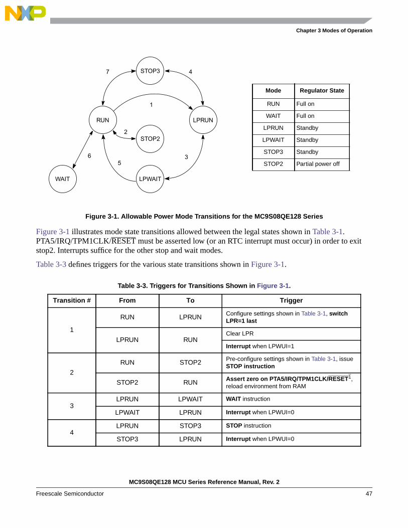
Chapter 3 Modes of Operation
Figure 3-1. Allowable Power Mode Transitions for the MC9S08QE128 Series
Figure 3-1 illustrates mode state transitions allowed between the legal states shown in Table 3-1.PTA5/IRQ/TPM1CLK/RESET must be asserted low (or an RTC interrupt must occur) in order to exitstop2. Interrupts suffice for the other stop and wait modes.
Table 3-3 defines triggers for the various state transitions shown in Figure 3-1.
Table 3-3. Triggers for Transitions Shown in Figure 3-1.
Transition # From To Trigger
1
RUN LPRUN Configure settings shown in Table 3-1, switchLPR=1 last
LPRUN RUNClear LPR
Interrupt when LPWUI=1
2
RUN STOP2 Pre-configure settings shown in Table 3-1, issueSTOP instruction
STOP2 RUN Assert zero on PTA5/IRQ/TPM1CLK/RESET1,reload environment from RAM
3LPRUN LPWAIT WAIT instruction
LPWAIT LPRUN Interrupt when LPWUI=0
4LPRUN STOP3 STOP instruction
STOP3 LPRUN Interrupt when LPWUI=0
Mode Regulator State
RUN Full on
WAIT Full on
LPRUN Standby
LPWAIT Standby
STOP3 Standby
STOP2 Partial power off
STOP3
STOP2
LPWAIT
LPRUNRUN
WAIT
7 4
1
35
2
6
MC9S08QE128 MCU Series Reference Manual, Rev. 2
Freescale Semiconductor 47
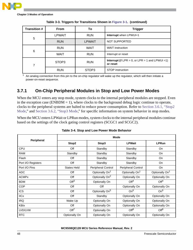
Chapter 3 Modes of Operation
3.7.1 On-Chip Peripheral Modules in Stop and Low Power Modes
When the MCU enters any stop mode, system clocks to the internal peripheral modules are stopped. Evenin the exception case (ENBDM = 1), where clocks to the background debug logic continue to operate,clocks to the peripheral systems are halted to reduce power consumption. Refer to Section 3.6.1, “Stop2Mode,” and Section 3.6.2, “Stop3 Mode,” for specific information on system behavior in stop modes.
When the MCU enters LPWait or LPRun modes, system clocks to the internal peripheral modules continuebased on the settings of the clock gating control registers (SCGC1 and SCGC2).
5LPWAIT RUN Interrupt when LPWUI=1
RUN LPWAIT NOT SUPPORTED
6RUN WAIT WAIT instruction
WAIT RUN Interrupt or reset
7STOP3 RUN Interrupt (if LPR = 0, or LPR = 1 and LPWUI =1)
or reset
RUN STOP3 STOP instruction
1 An analog connection from this pin to the on-chip regulator will wake up the regulator, which will then initiate apower-on-reset sequence.
Table 3-4. Stop and Low Power Mode Behavior
PeripheralMode
Stop2 Stop3 LPWait LPRun
CPU Off Standby Standby On
RAM Standby Standby Standby On
Flash Off Standby Standby On
Port I/O Registers Off Standby Standby On
Port I/O Pins States Held Peripheral Control Peripheral Control On
ADC Off Optionally On1 Optionally On1 Optionally On1
ACMPx Off Optionally On2 Optionally On Optionally On
BDM Off3 Optionally On Off4 Off4
COP Off Off Optionally On Optionally On
ICS Off Optionally On5 On6 On6
IICx Off Standby Optionally On Optionally On
IRQ Wake Up Optionally On Optionally On Optionally On
KBIx Off Optionally On Optionally On Optionally On
LVD/LVW Off7 Optionally On Off8 Off8
RTC Optionally On Optionally On Optionally On Optionally On
Table 3-3. Triggers for Transitions Shown in Figure 3-1. (continued)
Transition # From To Trigger
MC9S08QE128 MCU Series Reference Manual, Rev. 2
48 Freescale Semiconductor

Chapter 3 Modes of Operation
SCIx Off Standby Optionally On Optionally On
SPIx Off Standby Optionally On Optionally On
TPMx Off Standby Optionally On Optionally On
Voltage Regulator Partial Powerdown Optionally On9 Standby Standby
XOSC Optionally On Optionally On10 Optionally On Optionally On1 Requires the asynchronous ADC clock. For stop3, LVD must be enabled to run in stop if converting the bandgap channel.2 LVD must be enabled to run in stop if using the bandgap as a reference.3 If ENBDM is set when entering stop2, the MCU will actually enter stop3.4 If ENBDM is set when entering LPRun or LPWait, the MCU will actually stay in run mode or enter wait mode, respectively.5 IRCLKEN and IREFSTEN set in ICSC1, else in standby.6 ICS must be configured for FBELP, bus frequency limited to 125kHz in LPRUN or LPWAIT.7 If LVDSE is set when entering stop2, the MCU will actually enter stop3.8 If LVDSE is set when entering LPRun or LPWait, the MCU will actually enter run or wait mode, respectively.9 Requires the LVD to be enabled, else in standby. See Section 3.6.4, “LVD Enabled in Stop Mode”.10 ERCLKEN and EREFSTEN set in ICSC2, else in standby.
Table 3-4. Stop and Low Power Mode Behavior (continued)
PeripheralMode
Stop2 Stop3 LPWait LPRun
MC9S08QE128 MCU Series Reference Manual, Rev. 2
Freescale Semiconductor 49

Chapter 3 Modes of Operation
MC9S08QE128 MCU Series Reference Manual, Rev. 2
50 Freescale Semiconductor
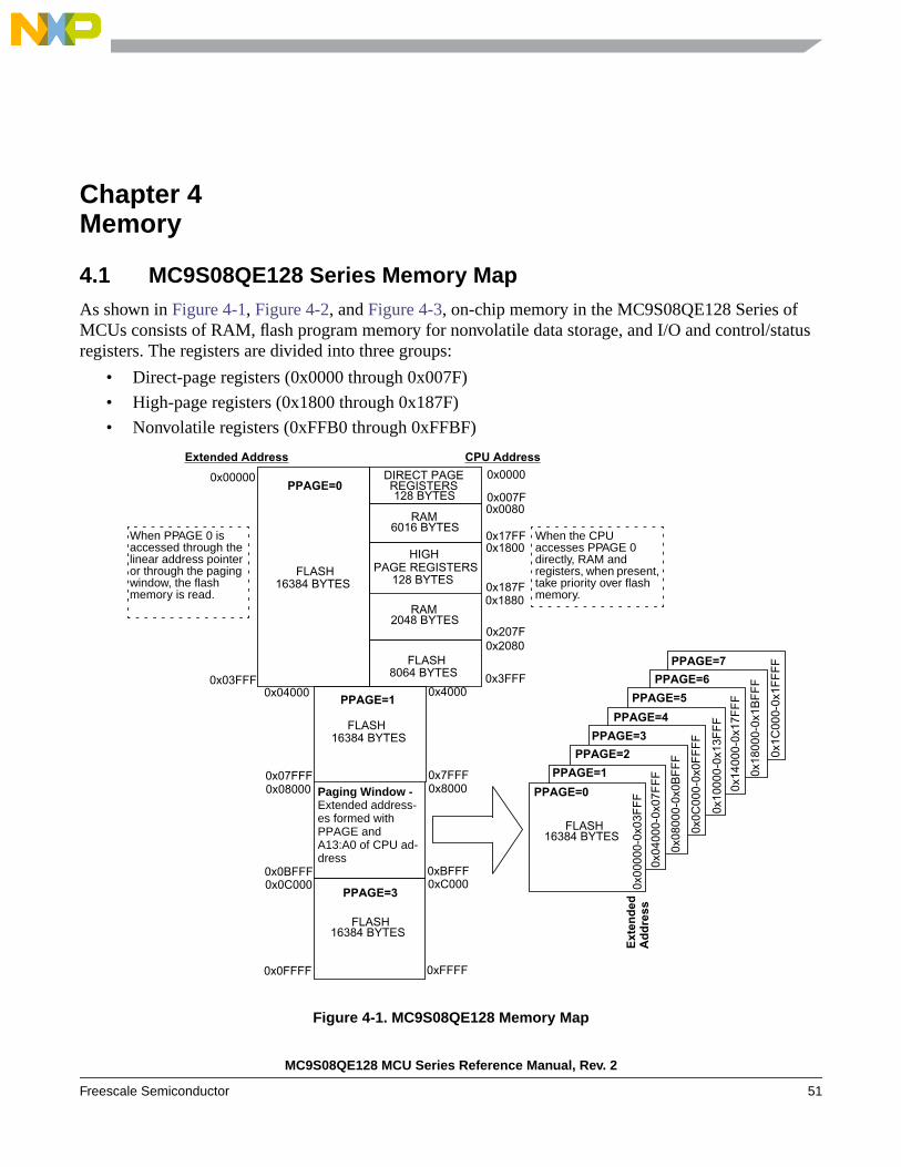
Chapter 4Memory
4.1 MC9S08QE128 Series Memory MapAs shown in Figure 4-1, Figure 4-2, and Figure 4-3, on-chip memory in the MC9S08QE128 Series ofMCUs consists of RAM, flash program memory for nonvolatile data storage, and I/O and control/statusregisters. The registers are divided into three groups:
• Direct-page registers (0x0000 through 0x007F)
• High-page registers (0x1800 through 0x187F)
• Nonvolatile registers (0xFFB0 through 0xFFBF)
Figure 4-1. MC9S08QE128 Memory Map
flash16384 BYTES
PPAGE=4
PPAGE=5
PPAGE=6
PPAGE=7
0x10
000-
0x13
FF
F
0x14
000-
0x17
FF
F
0x18
000-
0x1B
FF
F
0x1C
000-
0x1F
FF
F
DIRECT PAGE
RAM6016 BYTES
0x0000
0x007F0x0080
0x18000x17FF
0x187F
0x0FFFF
128 BYTES
HIGH
128 BYTES
FLASH16384 BYTES
0x1880RAM
2048 BYTES0x207F
0x3FFF
0x2080FLASH
8064 BYTES
16384 BYTES
0x07FFF
0x0C000
0x04000
REGISTERS
0x0BFFF
0x08000
PAGE REGISTERS
PPAGE=1
FLASH
16384 BYTES
PPAGE=0
FLASH
FLASH16384 BYTES
PPAGE=3
PPAGE=0
PPAGE=1
PPAGE=2
PPAGE=3
0x00000
0x03FFF
0x00
000-
0x03
FF
F
0x04
000-
0x07
FF
F
0x08
000-
0x0B
FF
F
0x0C
000-
0x0F
FF
F
When the CPUaccesses PPAGE 0directly, RAM andregisters, when present,take priority over flashmemory.
Extended Address CPU Address
Ext
end
edA
dd
ress
0xFFFF
0x7FFF
0xC000
0x4000
0xBFFF
0x8000Paging Window -Extended address-es formed withPPAGE andA13:A0 of CPU ad-dress
When PPAGE 0 isaccessed through thelinear address pointeror through the pagingwindow, the flashmemory is read.
MC9S08QE128 MCU Series Reference Manual, Rev. 2
Freescale Semiconductor 51

Chapter 4 Memory
Figure 4-2. MC9S08QE96 Memory Map
PPAGE=6
PPAGE=7
0x18
000-
0x1B
FF
F
0x1C
000-
0x1F
FF
F
Ext
end
edA
dd
ress
RESERVED16384 BYTES
FLASH16384 BYTES
PPAGE=4
PPAGE=5
0x10
000-
0x13
FF
F
0x14
000-
0x17
FF
F
DIRECT PAGE
RAM6016 BYTES
0x0000
0x007F0x0080
0x18000x17FF
0x187F
0x0FFFF
128 BYTES
HIGH
128 BYTES
FLASH16384 BYTES
0x1880RESERVED2048 BYTES
0x207F
0x3FFF
0x2080FLASH
8064 BYTES
16384 BYTES
0x07FFF
0x0C000
0x04000
REGISTERS
0x0BFFF
0x08000
PAGE REGISTERS
PPAGE=1
FLASH
16384 BYTES
PPAGE=0
FLASH
FLASH16384 BYTES
PPAGE=3
PPAGE=0
PPAGE=1
PPAGE=2
PPAGE=3
0x00000
0x03FFF
0x00
000-
0x03
FF
F
0x04
000-
0x07
FF
F
0x08
000-
0x0B
FF
F
0x0C
000-
0x0F
FF
F
When the CPUaccesses PPAGE 0directly, RAM andregisters, when present,take priority over flashmemory.
Extended Address CPU Address
Ext
end
edA
dd
ress
0xFFFF
0x7FFF
0xC000
0x4000
0xBFFF
0x8000Paging Window -Extendedaddresses formedwith PPAGE andA13:A0 of CPUaddress
When PPAGE 0 isaccessed through thelinear address pointeror through the pagingwindow, the flashmemory is read.
MC9S08QE128 MCU Series Reference Manual, Rev. 2
52 Freescale Semiconductor

Chapter 4 Memory
Figure 4-3. MC9S08QE64 Memory Map
4.2 Reset and Interrupt Vector Assignments
Table 4-1 shows address assignments for reset and interrupt vectors. The vector names shown in this tableare the labels used in the Freescale Semiconductor provided equate file for the MC9S08QE128 Series.
Table 4-1. Reset and Interrupt Vectors
Address(High/Low)
Vector Vector Name
0xFFC0:0xFFC1 TPM3 Overflow Vtpm3ovf
0xFFC2:0xFFC3 TPM3 Channel 5 Vtpm3ch5
0xFFC4:0xFFC5 TPM3 Channel 4 Vtpm3ch4
0xFFC6:0xFFC7 TPM3 Channel 3 Vtpm3ch3
0xFFC8:0xFFC9 TPM3 Channel 2 Vtpm3ch2
0xFFCA:0xFFCB TPM3 Channel 1 Vtpm3ch1
0xFFCC:0xFFCD TPM3 Channel 0 Vtpm3ch0
PPAGE=7
0x1C
000-
0x1F
FF
F
RESERVED16384 BYTES
PPAGE=6
RESERVED16384 BYTES
PPAGE=4
PPAGE=5
0x10
000-
0x13
FF
F
0x14
000-
0x17
FF
F
Ext
end
edA
dd
ress
RESERVED16384 BYTES 0x
1800
0-0x
1BF
FF
DIRECT PAGE
RAM4096 BYTES
0x0000
0x007F0x0080
0x10800x107F
0x187F
0x0FFFF
128 BYTES
HIGH
128 BYTES
FLASH16384 BYTES
0x1880RESERVED2048 BYTES 0x207F
0x3FFF
0x2080FLASH
8064 BYTES
16384 BYTES
0x07FFF
0x0C000
0x04000
REGISTERS
0x0BFFF
0x08000
PAGE REGISTERS
PPAGE=1
FLASH
16384 BYTES
PPAGE=0
FLASH
FLASH16384 BYTES
PPAGE=3
PPAGE=0
PPAGE=1
PPAGE=2
PPAGE=3
0x00000
0x03FFF
0x00
000-
0x03
FF
F
0x04
000-
0x07
FF
F
0x08
000-
0x0B
FF
F
0x0C
000-
0x0F
FF
F
When the CPUaccesses PPAGE 0directly, RAM andregisters, when present,take priority over flashmemory.
Extended Address CPU Address
Ext
end
edA
dd
ress
0xFFFF
0x7FFF
0xC000
0x4000
0xBFFF
0x8000Paging Window -Extendedaddresses formedwith PPAGE andA13:A0 of CPUaddress
When PPAGE 0 isaccessed through thelinear address pointeror through the pagingwindow, the flashmemory is read.
0x18000x17FF
RESERVED1920 BYTES
MC9S08QE128 MCU Series Reference Manual, Rev. 2
Freescale Semiconductor 53

Chapter 4 Memory
0xFFCE:0xFFCF RTC Vrtc
0xFFD0:0xFFD1 SCI2 Transmit Vsci2tx
0xFFD2:0xFFD3 SCI2 Receive Vsci2rx
0xFFD4:0xFFD5 SCI2 Error Vsci2err
0xFFD6:0xFFD7 ACMPx1 Vacmpx
0xFFD8:0xFFD9 ADC Conversion Vadc
0xFFDA:0xFFDB KBIx Interrupt2 Vkeyboard
0xFFDC:0xFFDD IICx3 Viicx
0xFFDE:0xFFDF SCI1 Transmit Vsci1tx
0xFFE0:0xFFE1 SCI1 Receive Vsci1rx
0xFFE2:0xFFE3 SCI1 Error Vsci1err
0xFFE4:0xFFE5 SPI1 Vspi1
0xFFE6:0xFFE7 SPI2 Vspi2
0xFFE8:0xFFE9 TPM2 Overflow Vtpm2ovf
0xFFEA:0xFFEB TPM2 Channel 2 Vtpm2ch2
0xFFEC:0xFFED TPM2 Channel 1 Vtpm2ch1
0xFFEE:0xFFEF TPM2 Channel 0 Vtpm2ch0
0xFFF0:0xFFF1 TPM1 Overflow Vtpm1ovf
0xFFF2:0xFFF3 TPM1 Channel 2 Vtpm1ch2
0xFFF4:0xFFF5 TPM1 Channel 1 Vtpm1ch1
0xFFF6:0xFFF7 TPM1 Channel 0 Vtpm1ch0
0xFFF8:0xFFF9 Low Voltage Detect or Low Voltage Warning Vlvd
0xFFFA:0xFFFB IRQ Virq
0xFFFC:0xFFFD SWI Vswi
0xFFFE:0xFFFF Reset Vreset
1 ACMP1 and ACMP2 share this vector, if both modules are enabled user should poll each flagto determine pending interrupt.
2 KBI1 and KBI2 share this vector, if both modules are enabled user should poll each flag todetermine pending interrupt.
3 IIC1 and IIC2 share this vector, if both modules are enabled user should poll each flag todetermine pending interrupt.
Table 4-1. Reset and Interrupt Vectors (continued)
Address(High/Low)
Vector Vector Name
MC9S08QE128 MCU Series Reference Manual, Rev. 2
54 Freescale Semiconductor

Chapter 4 Memory
4.3 Register Addresses and Bit AssignmentsThe registers in the MC9S08QE128 Series are divided into these groups:
• Direct-page registers are located in the first 128 locations in the memory map; these are accessiblewith efficient direct addressing mode instructions.
• High-page registers are used much less often, so they are located above 0x1800 in the memorymap. This leaves more room in the direct page for more frequently used registers and RAM.
• The nonvolatile register area consists of a block of 16 locations in flash memory at0xFFB0–0xFFBF. Nonvolatile register locations include:
— NVPROT and NVOPT are loaded into working registers at reset
— An 8-byte backdoor comparison key that optionally allows a user to gain controlled access tosecure memory
Because the nonvolatile register locations are flash memory, they must be erased and programmedlike other flash memory locations.
Direct-page registers can be accessed with efficient direct addressing mode instructions. Bit manipulationinstructions can be used to access any bit in any direct-page register. Table 4-2 is a summary of alluser-accessible direct-page registers and control bits.
The direct page registers in Table 4-2 can use the more efficient direct addressing mode, which requiresonly the lower byte of the address. Because of this, the lower byte of the address in column one is shownin bold text. In Table 4-3 and Table 4-4, the whole address in column one is shown in bold. In Table 4-2,Table 4-3, and Table 4-4, the register names in column two are shown in bold to set them apart from thebit names to the right. Cells that are not associated with named bits are shaded. A shaded cell with a 0indicates this unused bit always reads as a 0. Shaded cells with dashes indicate unused or reserved bitlocations that could read as 1s or 0s. When writing to these bits, write a 0 unless otherwise specified.
MC9S08QE128 MCU Series Reference Manual, Rev. 2
Freescale Semiconductor 55

Chapter 4 Memory
Table 4-2. Direct-Page Register Summary (Sheet 1 of 4)
AddressRegister
NameBit 7 6 5 4 3 2 1 Bit 0
0x0000 PTAD PTAD7 PTAD6 PTAD5 PTAD4 PTAD3 PTAD2 PTAD1 PTAD0
0x0001 PTADD PTADD7 PTADD6 PTADD5 PTADD4 PTADD3 PTADD2 PTADD1 PTADD0
0x0002 PTBD PTBD7 PTBD6 PTBD5 PTBD4 PTBD3 PTBD2 PTBD1 PTBD0
0x0003 PTBDD PTBDD7 PTBDD6 PTBDD5 PTBDD4 PTBDD3 PTBDD2 PTBDD1 PTBDD0
0x0004 PTCD PTCD7 PTCD6 PTCD5 PTCD4 PTCD3 PTCD2 PTCD1 PTCD0
0x0005 PTCDD PTCDD7 PTCDD6 PTCDD5 PTCDD4 PTCDD3 PTCDD2 PTCDD1 PTCDD0
0x0006 PTDD PTDD7 PTDD6 PTDD5 PTDD4 PTDD3 PTDD2 PTDD1 PTDD0
0x0007 PTDDD PTDDD7 PTDDD6 PTDDD5 PTDDD4 PTDDD3 PTDDD2 PTDDD1 PTDDD0
0x0008 PTED PTED7 PTED6 PTED5 PTED4 PTED3 PTED2 PTED1 PTED0
0x0009 PTEDD PTEDD7 PTEDD6 PTEDD5 PTEDD4 PTEDD3 PTEDD2 PTEDD1 PTEDD0
0x000A PTFD PTFD7 PTFD6 PTFD5 PTFD4 PTFD3 PTFD2 PTFD1 PTFD0
0x000B PTFDD PTFDD7 PTFDD6 PTFDD5 PTFDD4 PTFDD3 PTFDD2 PTFDD1 PTFDD0
0x000C KBI1SC 0 0 0 0 KBF KBACK KBIE KBIMOD
0x000D KBI1PE KBIPE7 KBIPE6 KBIPE5 KBIPE4 KBIPE3 KBIPE2 KBIPE1 KBIPE0
0x000E KBI1ES KBEDG7 KBEDG6 KBEDG5 KBEDG4 KBEDG3 KBEDG2 KBEDG1 KBEDG0
0x000F IRQSC 0 IRQPDD IRQEDG IRQPE IRQF IRQACK IRQIE IRQMOD
0x0010 ADCSC1 COCO AIEN ADCO ADCH
0x0011 ADCSC2 ADACT ADTRG ACFE ACFGT — — Reserved Reserved
0x0012 ADCRH 0 0 0 0 ADR11 ADR10 ADR9 ADR8
0x0013 ADCRL ADR7 ADR6 ADR5 ADR4 ADR3 ADR2 ADR1 ADR0
0x0014 ADCCVH 0 0 0 0 ADCV11 ADCV10 ADCV9 ADCV8
0x0015 ADCCVL ADCV7 ADCV6 ADCV5 ADCV4 ADCV3 ADCV2 ADCV1 ADCV0
0x0016 ADCCFG ADLPC ADIV ADLSMP MODE ADICLK
0x0017 APCTL1 ADPC7 ADPC6 ADPC5 ADPC4 ADPC3 ADPC2 ADPC1 ADPC0
0x0018 APCTL2 ADPC15 ADPC14 ADPC13 ADPC12 ADPC11 ADPC10 ADPC9 ADPC8
0x0019 APCTL3 ADPC23 ADPC22 ADPC21 ADPC20 ADPC19 ADPC18 ADPC17 ADPC16
0x001A ACMP1SC ACME ACBGS ACF ACIE ACO ACOPE ACMOD
0x001B ACMP2SC ACME ACBGS ACF ACIE ACO ACOPE ACMOD
0x001C PTGD PTGD7 PTGD6 PTGD5 PTGD4 PTGD3 PTGD2 PTGD1 PTGD0
0x001D PTGDD PTGDD7 PTGDD6 PTGDD5 PTGDD4 PTGDD3 PTGDD2 PTGDD1 PTGDD0
0x001E PTHD PTHD7 PTHD6 PTHD5 PTHD4 PTHD3 PTHD2 PTHD1 PTHD0
0x001F PTHDD PTHDD7 PTHDD6 PTHDD5 PTHDD4 PTHDD3 PTHDD2 PTHDD1 PTHDD0
0x0020 SCI1BDH LBKDIE RXEDGIE 0 SBR12 SBR11 SBR10 SBR9 SBR8
0x0021 SCI1BDL SBR7 SBR6 SBR5 SBR4 SBR3 SBR2 SBR1 SBR0
0x0022 SCI1C1 LOOPS SCISWAI RSRC M WAKE ILT PE PT
0x0023 SCI1C2 TIE TCIE RIE ILIE TE RE RWU SBK
0x0024 SCI1S1 TDRE TC RDRF IDLE OR NF FE PF
0x0025 SCI1S2 LBKDIF RXEDGIF 0 RXINV RWUID BRK13 LBKDE RAF
0x0026 SCI1C3 R8 T8 TXDIR TXINV ORIE NEIE FEIE PEIE
0x0027 SCI1D Bit 7 6 5 4 3 2 1 Bit 0
0x0028 SPI1C1 SPIE SPE SPTIE MSTR CPOL CPHA SSOE LSBFE
0x0029 SPI1C2 0 0 0 MODFEN BIDIROE 0 SPISWAI SPC0
MC9S08QE128 MCU Series Reference Manual, Rev. 2
56 Freescale Semiconductor
Chapter 4 Memory
0x002A SPI1BR 0 SPPR2 SPPR1 SPPR0 0 SPR2 SPR1 SPR0
0x002B SPI1S SPRF 0 SPTEF MODF 0 0 0 0
0x002C Reserved 0 0 0 0 0 0 0 0
0x002D SPI1D Bit 7 6 5 4 3 2 1 Bit 0
0x002E PTJD PTJD7 PTJD6 PTJD5 PTJD4 PTJD3 PTJD2 PTJD1 PTJD0
0x002F PTJDD PTJDD7 PTJDD6 PTJDD5 PTJDD4 PTJDD3 PTJDD2 PTJDD1 PTJDD0
0x0030 IIC1A AD7 AD6 AD5 AD4 AD3 AD2 AD1 0
0x0031 IIC1F MULT ICR
0x0032 IIC1C1 IICEN IICIE MST TX TXAK RSTA 0 0
0x0033 IIC1S TCF IAAS BUSY ARBL 0 SRW IICIF RXAK
0x0034 IIC1D DATA
0x0035 IIC1C2 GCAEN ADEXT 0 0 0 AD10 AD9 AD8
0x0036 Reserved — — — — — — — —
0x0037 Reserved — — — — — — — —
0x0038 ICSC1 CLKS RDIV IREFS IRCLKEN IREFSTEN
0x0039 ICSC2 BDIV RANGE HGO LP EREFS ERCLKEN EREFSTEN
0x003A ICSTRM TRIM
0x003B ICSSC DRS/DRST DMX32 IREFST CLKST OSCINIT FTRIM
0x003C KBI2SC 0 0 0 0 KBF KBACK KBIE KBIMOD
0x003D KBI2PE KBIPE7 KBIPE6 KBIPE5 KBIPE4 KBIPE3 KBIPE2 KBIPE1 KBIPE0
0x003E KBI2ES KBEDG7 KBEDG6 KBEDG5 KBEDG4 KBEDG3 KBEDG2 KBEDG1 KBEDG0
0x003F Reserved — — — — — — — —
0x0040 TPM1SC TOF TOIE CPWMS CLKSB CLKSA PS2 PS1 PS0
0x0041 TPM1CNTH Bit 15 14 13 12 11 10 9 Bit 8
0x0042 TPM1CNTL Bit 7 6 5 4 3 2 1 Bit 0
0x0043 TPM1MODH Bit 15 14 13 12 11 10 9 Bit 8
0x0044 TPM1MODL Bit 7 6 5 4 3 2 1 Bit 0
0x0045 TPM1C0SC CH0F CH0IE MS0B MS0A ELS0B ELS0A 0 0
0x0046 TPM1C0VH Bit 15 14 13 12 11 10 9 Bit 8
0x0047 TPM1C0VL Bit 7 6 5 4 3 2 1 Bit 0
0x0048 TPM1C1SC CH1F CH1IE MS1B MS1A ELS1B ELS1A 0 0
0x0049 TPM1C1VH Bit 15 14 13 12 11 10 9 Bit 8
0x004A TPM1C1VL Bit 7 6 5 4 3 2 1 Bit 0
0x004B TPM1C2SC CH2F CH2IE MS2B MS2A ELS2B ELS2A 0 0
0x004C TPM1C2VH Bit 15 14 13 12 11 10 9 Bit 8
0x004D TPM1C2VL Bit 7 6 5 4 3 2 1 Bit 0
0x004E-0x004F
Reserved ——
——
——
——
——
——
——
——
0x0050 TPM2SC TOF TOIE CPWMS CLKSB CLKSA PS2 PS1 PS0
0x0051 TPM2CNTH Bit 15 14 13 12 11 10 9 Bit 8
0x0052 TPM2CNTL Bit 7 6 5 4 3 2 1 Bit 0
0x0053 TPM2MODH Bit 15 14 13 12 11 10 9 Bit 8
Table 4-2. Direct-Page Register Summary (Sheet 2 of 4)
AddressRegister
NameBit 7 6 5 4 3 2 1 Bit 0
MC9S08QE128 MCU Series Reference Manual, Rev. 2
Freescale Semiconductor 57
Chapter 4 Memory
0x0054 TPM2MODL Bit 7 6 5 4 3 2 1 Bit 0
0x0055 TPM2C0SC CH0F CH0IE MS0B MS0A ELS0B ELS0A 0 0
0x0056 TPM2C0VH Bit 15 14 13 12 11 10 9 Bit 8
0x0057 TPM2C0VL Bit 7 6 5 4 3 2 1 Bit 0
0x0058 TPM2C1SC CH1F CH1IE MS1B MS1A ELS1B ELS1A 0 0
0x0059 TPM2C1VH Bit 15 14 13 12 11 10 9 Bit 8
0x005A TPM2C1VL Bit 7 6 5 4 3 2 1 Bit 0
0x005B TPM2C2SC CH2F CH2IE MS2B MS2A ELS2B ELS2A 0 0
0x005C TPM2C2VH Bit 15 14 13 12 11 10 9 Bit 8
0x005D TPM2C2VL Bit 7 6 5 4 3 2 1 Bit 0
0x005E-0x005F
Reserved ——
——
——
——
——
——
——
——
0x0060 TPM3SC TOF TOIE CPWMS CLKSB CLKSA PS2 PS1 PS0
0x0061 TPM3CNTH Bit 15 14 13 12 11 10 9 Bit 8
0x0062 TPM3CNTL Bit 7 6 5 4 3 2 1 Bit 0
0x0063 TPM3MODH Bit 15 14 13 12 11 10 9 Bit 8
0x0064 TPM3MODL Bit 7 6 5 4 3 2 1 Bit 0
0x0065 TPM3C0SC CH0F CH0IE MS0B MS0A ELS0B ELS0A 0 0
0x0066 TPM3C0VH Bit 15 14 13 12 11 10 9 Bit 8
0x0067 TPM3C0VL Bit 7 6 5 4 3 2 1 Bit 0
0x0068 TPM3C1SC CH1F CH1IE MS1B MS1A ELS1B ELS1A 0 0
0x0069 TPM3C1VH Bit 15 14 13 12 11 10 9 Bit 8
0x006A TPM3C1VL Bit 7 6 5 4 3 2 1 Bit 0
0x006B TPM3C2SC CH2F CH2IE MS2B MS2A ELS2B ELS2A 0 0
0x006C TPM3C2VH Bit 15 14 13 12 11 10 9 Bit 8
0x006D TPM3C2VL Bit 7 6 5 4 3 2 1 Bit 0
0x006E TPM3C3SC CH3F CH3IE MS3B MS3A ELS3B ELS3A 0 0
0x006F TPM3C3VH Bit 15 14 13 12 11 10 9 Bit 8
0x0070 TPM3C3VL Bit 7 6 5 4 3 2 1 Bit 0
0x0071 TPM3C4SC CH4F CH4IE MS4B MS4A ELS4B ELS4A 0 0
0x0072 TPM3C4VH Bit 15 14 13 12 11 10 9 Bit 8
0x0073 TPM3C4VL Bit 7 6 5 4 3 2 1 Bit 0
0x0074 TPM3C5SC CH5F CH5IE MS5B MS5A ELS5B ELS5A 0 0
0x0075 TPM3C5VH Bit 15 14 13 12 11 10 9 Bit 8
0x0076 TPM3C5VL Bit 7 6 5 4 3 2 1 Bit 0
0x0077 Reserved — — — — — — — —
0x0078 PPAGE 0 0 0 0 0 XA16 XA15 XA14
0x0079 LAP2 0 0 0 0 0 0 0 LA16
Table 4-2. Direct-Page Register Summary (Sheet 3 of 4)
AddressRegister
NameBit 7 6 5 4 3 2 1 Bit 0
MC9S08QE128 MCU Series Reference Manual, Rev. 2
58 Freescale Semiconductor
Chapter 4 Memory
High-page registers, shown in Table 4-3, are accessed much less often than other I/O and control registersso they have been located outside the direct addressable memory space, starting at 0x1800.
0x007A LAP1 LA15 LA14 LA13 LA12 LA11 LA10 LA9 LA8
0x007B LAP0 LA7 LA6 LA5 LA4 LA3 LA2 LA1 LA0
0x007C LWP D7 D6 D5 D4 D3 D2 D1 D0
0x007D LBP D7 D6 D5 D4 D3 D2 D1 D0
0x007E LB D7 D6 D5 D4 D3 D2 D1 D0
0x007F LAPAB D7 D6 D5 D4 D3 D2 D1 D0
Table 4-3. High-Page Register Summary (Sheet 1 of 4)
Address Register Name Bit 7 6 5 4 3 2 1 Bit 0
0x1800 SRS POR PIN COP ILOP 0 0 LVD 0
0x1801 SBDFR 0 0 0 0 0 0 0 BDFR
0x1802 SOPT1 COPE COPT STOPE — 0 RSTPOE BKGDPE RSTPE
0x1803 SOPT2 COPCLKS 0 0 0 SPI1PS ACIC2 IIC1PS ACIC1
0x1804 –0x1805
Reserved ——
——
——
——
——
——
——
——
0x1806 SDIDH — — — — ID11 ID10 ID9 ID8
0x1807 SDIDL ID7 ID6 ID5 ID4 ID3 ID2 ID1 ID0
0x1808 SPMSC1 LVDF LVDACK LVDIE LVDRE LVDSE LVDE 0 BGBE
0x1809 SPMSC2 LPR LPRS LPWUI 0 PPDF PPDACK PPDE PPDC
0x180A Reserved — — — — — — — —
0x180B SPMSC3 LVWF LVWACK LVDV LVWV LVWIE — — —
0x180C Reserved — — — — — — — —
0x180D Reserved — — — — — — — —
0x180E SCGC1 TPM3 TPM2 TPM1 ADC IIC2 IIC1 SCI2 SCI1
0x180F SCGC2 DBG FLS IRQ KBI ACMP RTC SPI2 SPI1
0x1810 DBGCAH Bit 15 14 13 12 11 10 9 Bit 8
0x1811 DBGCAL Bit 7 6 5 4 3 2 1 Bit 0
0x1812 DBGCBH Bit 15 14 13 12 11 10 9 Bit 8
0x1813 DBGCBL Bit 7 6 5 4 3 2 1 Bit 0
0x1814 DBGCCH Bit 15 14 13 12 11 10 9 Bit 8
0x1815 DBGCCL Bit 7 6 5 4 3 2 1 Bit 0
0x1816 DBGFH Bit 15 14 13 12 11 10 9 Bit 8
0x1817 DBGFL Bit 7 6 5 4 3 2 1 Bit 0
0x1818 DBGCAX RWAEN RWA PAGSEL 0 0 0 0 Bit 16
0x1819 DBGCBX RWBEN RWB PAGSEL 0 0 0 0 Bit 16
0x181A DBGCCX RWCEN RWC PAGSEL 0 0 0 0 Bit 16
0x181B DBGFX PPACC 0 0 0 0 0 0 Bit 16
0x181C DBGC DBGEN ARM TAG BRKEN 0 0 0 LOOP1
0x181D DBGT TRGSEL BEGIN 0 0 TRG
0x181E DBGS AF BF CF 0 0 0 0 ARMF
Table 4-2. Direct-Page Register Summary (Sheet 4 of 4)
AddressRegister
NameBit 7 6 5 4 3 2 1 Bit 0
MC9S08QE128 MCU Series Reference Manual, Rev. 2
Freescale Semiconductor 59

Chapter 4 Memory
0x181F DBGCNT 0 0 0 0 CNT
0x1820 FCDIV FDIVLD PRDIV8 FDIV
0x1821 FOPT KEYEN 0 0 0 0 SEC
0x1822 Reserved — — — — — — — —
0x1823 FCNFG 0 0 KEYACC 0 0 0 0 0
0x1824 FPROT FPS FPOPEN
0x1825 FSTAT FCBEF FCCF FPVIOL FACCERR 0 FBLANK 0 0
0x1826 FCMD 0 FCMD
0x1827-0x1829
Reserved ——
——
——
——
——
——
——
——
0x182A Reserved
0x182B-0x182F
Reserved— — — — — — — —
0x1830 RTCSC RTIF RTCLKS RTIE RTCPS
0x1831 RTCCNT RTCCNT
0x1832 RTCMOD RTCMOD
0x1833-0x1837
Reserved ——
——
——
——
——
——
——
——
0x1838 SPI2C1 SPIE SPE SPTIE MSTR CPOL CPHA SSOE LSBFE
0x1839 SPI2C2 0 0 0 MODFEN BIDIROE 0 SPISWAI SPC0
0x183A SPI2BR 0 SPPR2 SPPR1 SPPR0 0 SPR2 SPR1 SPR0
0x183B SPI2S SPRF 0 SPTEF MODF 0 0 0 0
0x183C Reserved 0 0 0 0 0 0 0 0
0x183D SPI2D Bit 7 6 5 4 3 2 1 Bit 0
0x183E-0x183F
Reserved ——
——
——
——
——
——
——
——
0x1840 PTAPE PTAPE7 PTAPE6 PTAPE5 PTAPE4 PTAPE3 PTAPE2 PTAPE1 PTAPE0
0x1841 PTASE PTASE7 PTASE6 PTASE5 PTASE4 PTASE3 PTASE2 PTASE1 PTASE0
0x1842 PTADS PTADS7 PTADS6 PTADS5 PTADS4 PTADS3 PTADS2 PTADS1 PTADS0
0x1843 Reserved — — — — — — — —
0x1844 PTBPE PTBPE7 PTBPE6 PTBPE5 PTBPE4 PTBPE3 PTBPE2 PTBPE1 PTBPE0
0x1845 PTBSE PTBSE7 PTBSE6 PTBSE5 PTBSE4 PTBSE3 PTBSE2 PTBSE1 PTBSE0
0x1846 PTBDS PTBDS7 PTBDS6 PTBDS5 PTBDS4 PTBDS3 PTBDS2 PTBDS1 PTBDS0
0x1847 Reserved — — — — — — — —
0x1848 PTCPE PTCPE7 PTCPE6 PTCPE5 PTCPE4 PTCPE3 PTCPE2 PTCPE1 PTCPE0
0x1849 PTCSE PTCSE7 PTCSE6 PTCSE5 PTCSE4 PTCSE3 PTCSE2 PTCSE1 PTCSE0
0x184A PTCDS PTCDS7 PTCDS6 PTCDS5 PTCDS4 PTCDS3 PTCDS2 PTCDS1 PTCDS0
0x184B Reserved — — — — — — — —
0x184C PTDPE PTDPE7 PTDPE6 PTDPE5 PTDPE4 PTDPE3 PTDPE2 PTDPE1 PTDPE0
0x184D PTDSE PTDSE7 PTDSE6 PTDSE5 PTDSE4 PTDSE3 PTDSE2 PTDSE1 PTDSE0
0x184E PTDDS PTDDS7 PTDDS6 PTDDS5 PTDDS4 PTDDS3 PTDDS2 PTDDS1 PTDDS0
0x184F Reserved — — — — — — — —
0x1850 PTEPE PTEPE7 PTEPE6 PTEPE5 PTEPE4 PTEPE3 PTEPE2 PTEPE1 PTEPE0
Table 4-3. High-Page Register Summary (Sheet 2 of 4)
Address Register Name Bit 7 6 5 4 3 2 1 Bit 0
MC9S08QE128 MCU Series Reference Manual, Rev. 2
60 Freescale Semiconductor

Chapter 4 Memory
0x1851 PTESE PTESE7 PTESE6 PTESE5 PTESE4 PTESE3 PTESE2 PTESE1 PTESE0
0x1852 PTEDS PTEDS7 PTEDS6 PTEDS5 PTEDS4 PTEDS3 PTEDS2 PTEDS1 PTEDS0
0x1853 Reserved — — — — — — — —
0x1854 PTFPE PTFPE7 PTFPE6 PTFPE5 PTFPE4 PTFPE3 PTFPE2 PTFPE1 PTFPE0
0x1855 PTFSE PTFSE7 PTFSE6 PTFSE5 PTFSE4 PTFSE3 PTFSE2 PTFSE1 PTFSE0
0x1856 PTFDS PTFDS7 PTFDS6 PTFDS5 PTFDS4 PTFDS3 PTFDS2 PTFDS1 PTFDS0
0x1857 Reserved — — — — — — — —
0x1858 PTGPE PTGPE7 PTGPE6 PTGPE5 PTGPE4 PTGPE3 PTGPE2 PTGPE1 PTGPE0
0x1859 PTGSE PTGSE7 PTGSE6 PTGSE5 PTGSE4 PTGSE3 PTGSE2 PTGSE1 PTGSE0
0x185A PTGDS PTGDS7 PTGDS6 PTGDS5 PTGDS4 PTGDS3 PTGDS2 PTGDS1 PTGDS0
0x185B Reserved — — — — — — — —
0x185C PTHPE PTHPE7 PTHPE6 PTHPE5 PTHPE4 PTHPE3 PTHPE2 PTHPE1 PTHPE0
0x185D PTHSE PTHSE7 PTHSE6 PTHSE5 PTHSE4 PTHSE3 PTHSE2 PTHSE1 PTHSE0
0x185E PTHDS PTHDS7 PTHDS6 PTHDS5 PTHDS4 PTHDS3 PTHDS2 PTHDS1 PTHDS0
0x185F Reserved — — — — — — — —
0x1860 PTJPE PTJPE7 PTJPE6 PTJPE5 PTJPE4 PTJPE3 PTJPE2 PTJPE1 PTJPE0
0x1861 PTJSE PTJSE7 PTJSE6 PTJSE5 PTJSE4 PTJSE3 PTJSE2 PTJSE1 PTJSE0
0x1862 PTJDS PTJDS7 PTJDS6 PTJDS5 PTJDS4 PTJDS3 PTJDS2 PTJDS1 PTJDS0
0x1863–0x1867
Reserved ——
——
——
——
——
——
——
——
0x1868 IIC2A AD7 AD6 AD5 AD4 AD3 AD2 AD1 0
0x1869 IIC2F MULT ICR
0x186A IIC2C1 IICEN IICIE MST TX TXAK RSTA 0 0
0x186B IIC2S TCF IAAS BUSY ARBL 0 SRW IICIF RXAK
0x186C IIC2D DATA
0x186D IIC2C2 GCAEN ADEXT 0 0 0 AD10 AD9 AD8
0x186E–0x186F
Reserved ——
——
——
——
——
——
——
——
0x1870 SCI2BDH LBKDIE RXEDGIE 0 SBR12 SBR11 SBR10 SBR9 SBR8
0x1871 SCI2BDL SBR7 SBR6 SBR5 SBR4 SBR3 SBR2 SBR1 SBR0
0x1872 SCI2C1 LOOPS SCISWAI RSRC M WAKE ILT PE PT
0x1873 SCI2C2 TIE TCIE RIE ILIE TE RE RWU SBK
0x1874 SCI2S1 TDRE TC RDRF IDLE OR NF FE PF
0x1875 SCI2S2 LBKDIF RXEDGIF 0 RXINV RWUID BRK13 LBKDE RAF
0x1876 SCI2C3 R8 T8 TXDIR TXINV ORIE NEIE FEIE PEIE
0x1877 SCI2D Bit 7 6 5 4 3 2 1 Bit 0
0x1878 PTCSET PTCSET7 PTCSET6 PTCSET5 PTCSET4 PTCSET3 PTCSET2 PTCSET1 PTCSET0
0x1879 PTESET PTESET7 PTESET6 PTESET5 PTESET4 PTESET3 PTESET2 PTESET1 PTESET0
0x187A PTCCLR PTCCLR7 PTCCLR6 PTCCLR5 PTCCLR4 PTCCLR3 PTCCLR2 PTCCLR1 PTCCLR0
0x187B PTECLR PTECLR7 PTECLR6 PTECLR5 PTECLR4 PTECLR3 PTECLR2 PTECLR1 PTECLR0
0x187C PTCTOG PTCTOG7 PTCTOG6 PTCTOG5 PTCTOG4 PTCTOG3 PTCTOG2 PTCTOG1 PTCTOG0
Table 4-3. High-Page Register Summary (Sheet 3 of 4)
Address Register Name Bit 7 6 5 4 3 2 1 Bit 0
MC9S08QE128 MCU Series Reference Manual, Rev. 2
Freescale Semiconductor 61

Chapter 4 Memory
Several reserved flash memory locations, shown in Table 4-4, are used for storing values used by severalregisters. These registers include an 8-byte backdoor key, NVBACKKEY, which can be used to gain accessto secure memory resources. During reset events, the contents of NVPROT and NVOPT in the reservedflash memory are transferred into corresponding FPROT and FOPT registers in the high-page registersarea to control security and block protection options.
The factory ICS trim value is stored in the flash information row (IFR1) and will be loaded into theICSTRM and ICSSC registers after any reset. The internal reference trim values stored in flash, TRIM andFTRIM, can be programmed by third party programmers and must be copied into the corresponding ICSregisters by user code to override the factory trim.
NOTEWhen the MCU is in active BDM, the trim value in the IFR will not beloaded. Instead, the ICSTRM register will reset to 0x80 and the FTRIM bitin the ICSSC register will be reset to 0.
Provided the key enable (KEYEN) bit is 1, the 8-byte comparison key can be used to temporarilydisengage memory security. This key mechanism can be accessed only through user code running in securememory. (A security key cannot be entered directly through background debug commands.) This securitykey can be disabled completely by programming the KEYEN bit to 0. If the security key is disabled, theonly way to disengage security is by mass erasing the flash if needed (normally through the background
0x187D PTETOG PTETOG7 PTETOG6 PTETOG5 PTETOG4 PTETOG3 PTETOG2 PTETOG1 PTETOG0
0x187E–0x187F
Reserved ——
——
——
——
——
——
——
——
1. IFR — Nonvolatile information memory that can be only accessed during production test. During production test, systeminitialization, configuration and test information is stored in the IFR. This information cannot be read or modified in normal useror background debug modes.
Table 4-4. Reserved Flash Memory Addresses
Address Register Name Bit 7 6 5 4 3 2 1 Bit 0
0xFFAE Reserved forStorage of FTRIM
0 0 0 0 0 0 0 FTRIM
0xFFAF Reserved forStorage ofICSTRM
TRIM
0xFFB0 –0xFFB7
NVBACKKEY8-Byte Comparison Key
0xFFB8 –0xFFBC
Reserved ——
——
——
——
——
——
——
——
0xFFBD NVPROT FPS FPOPEN
0xFFBE Reserved — — — — — — — —
0xFFBF NVOPT KEYEN 0 0 0 0 SEC
Table 4-3. High-Page Register Summary (Sheet 4 of 4)
Address Register Name Bit 7 6 5 4 3 2 1 Bit 0
MC9S08QE128 MCU Series Reference Manual, Rev. 2
62 Freescale Semiconductor
Chapter 4 Memory
debug interface) and verifying that flash is blank. To avoid returning to secure mode after the next reset,program the security bits (SEC) to the unsecured state (1:0).
4.4 Memory Management Unit
The memory management unit (MMU) allows the program and data space for the HCS08 Family ofmicrocontrollers to be extended beyond the 64K byte CPU addressable memory map. The MMU uses apaging scheme similar to that seen on other MCU architectures, such as HCS12. The extended memorywhen used for data can also be accessed linearly using a linear address pointer and data access registers.
4.4.1 Features
Key features of the MMU module are:
• Memory Management Unit extends the HCS08 memory space
— up to 4 MB for program and data space
• Extended program space using paging scheme
— PPAGE register used for page selection
— fixed 16K byte memory window
— architecture supports up to 256, 16K pages
• Extended data space using linear address pointer
— up to 22-bit linear address pointer
— linear address pointer and data register provided in direct page allows access of complete flashmemory map using direct page instructions
— optional auto increment of pointer when data accessed
— supports an 2s compliment addition/subtraction to address pointer without using any mathinstructions or memory resources
— supports word accesses to any address specified by the linear address pointer when usingLDHX, STHX instructions
4.4.2 Register Definition
4.4.2.1 Program Page Register (PPAGE)
The HCS08 Core architecture limits the CPU addressable space available to 64K bytes. The address spacecan be extended to 128K bytes using a paging window scheme. The Program Page (PPAGE) allows forselecting one of the 16K byte blocks to be accessed through the Program Page Window located at0x8000-0xBFFF. The CALL and RTC instructions can load or store the value of PPAGE onto or from thestack during program execution. After any reset, PPAGE is set to PAGE 2.
MC9S08QE128 MCU Series Reference Manual, Rev. 2
Freescale Semiconductor 63
Chapter 4 Memory
4.4.2.2 Linear Address Pointer Registers 2:0 (LAP2:LAP0)
The three registers, LAP2:LAP0 contain the 17-bit linear address that allows the user to access any flashlocation in the extended address map. This register is used in conjunction with the data registers, linearbyte (LB), linear byte post increment (LBP) and linear word post increment (LWP). The contents ofLAP2:LAP0 will auto-increment when accessing data using the LBP and LWP registers. The contents ofLAP2:LAP0 can be increased by writing an 8-bit value to LAPAB.
4.4.2.3 Linear Word Post Increment Register (LWP)
This register is one of three data registers that the user can use to access any flash memory location in theextended address map. When LWP is accessed the contents of LAP2:LAP0 make up the extended addressof the flash memory location to be addressed. When accessing data using LWP, the contents ofLAP2:LAP0 will increment after the read or write is complete.
7 6 5 4 3 2 1 0
R 0 0 0 0 0XA16 XA15 XA14
W
Reset: 0 0 0 0 0 0 1 0
Figure 4-4. Program Page Register (PPAGE)
Table 4-5. Program Page Register Field Descriptions
Field Description
2:0XA16:XA14
When the CPU addresses the paging window, 0x8000-0xBFFF, the value in the PPAGE register along with theCPU addresses A13:A0 are used to create a 17-bit extended address.
7 6 5 4 3 2 1 0
R 0 0 0 0 0 0 0LA16
W
RLA15 LA14 LA13 LA12 LA11 LA10 LA9 LA8
W
RLA7 LA6 LA5 LA4 LA3 LA2 LA1 LA0
W
Reset: 0 0 0 0 0 0 0 0
Figure 4-5. Linear Address Pointer Registers 2:0 (LAP2:LAP0)
Table 4-6. Linear Address Pointer Registers 2:0 Field Descriptions
Field Description
16:0LA21:LA0
The values in LAP2:LAP0 are used to create a 17-bit linear address pointer. The value in these registers are usedas the extended address when accessing any of the data registers LB, LBP and LWP.
MC9S08QE128 MCU Series Reference Manual, Rev. 2
64 Freescale Semiconductor

Chapter 4 Memory
Accessing LWP does the same thing as accessing LBP. The MMU register ordering of LWP followed byLBP, allow the user to access data by words using the LDHX or STHX instructions of the LWP register.
4.4.2.4 Linear Byte Post Increment Register (LBP)
This register is one of three data registers that the user can use to access any flash memory location in theextended address map. When LBP is accessed the contents of LAP2:LAP0 make up the extended addressof the flash memory location to be addressed. When accessing data using LBP, the contents of LAP2:LAP0will increment after the read or write is complete.
Accessing LBP does the same thing as accessing LWP. The MMU register ordering of LWP followed byLBP, allow the user to access data by words using the LDHX or STHX instructions with the address of theLWP register.
7 6 5 4 3 2 1 0
RD7 D6 D5 D4 D3 D2 D1 D0
W
Reset: 0 0 0 0 0 0 0 0
Figure 4-6. Linear Word Post Increment Register (LWP)
Table 4-7. Linear Word Post Increment Register Field Descriptions
Field Description
7:0D7:D0
Reads of this register will first return the data value pointed to by the linear address pointer, LAP2:LAP0 and thenwill increment LAP2:LAP0. Writes to this register will first write the data value to the memory location specifiedby the linear address pointer and then will increment LAP2:LAP0. Writes to this register are most commonly usedwhen writing to the flash block(s) during programming.
7 6 5 4 3 2 1 0
RD7 D6 D5 D4 D3 D2 D1 D0
W
Reset: 0 0 0 0 0 0 0 0
Figure 4-7. Linear Byte Post Increment Register (LBP)
Table 4-8. Linear Byte Post Increment Register Field Descriptions
Field Description
7:0D7:D0
Reads of this register will first return the data value pointed to by the linear address pointer, LAP2:LAP0 and thenwill increment LAP2:LAP0. Writes to this register will first write the data value to the memory location specifiedby the linear address pointer and then will increment LAP2:LAP0. Writes to this register are most commonly usedwhen writing to the flash block(s) during programming.
MC9S08QE128 MCU Series Reference Manual, Rev. 2
Freescale Semiconductor 65

Chapter 4 Memory
4.4.2.5 Linear Byte Register (LB)
This register is one of three data registers that the user can use to access any flash memory location in theextended address map. When LB is accessed the contents of LAP2:LAP0 make up the extended addressof the flash memory location to be addressed.
4.4.2.6 Linear Address Pointer Add Byte Register (LAPAB)
The user can increase or decrease the contents of LAP2:LAP0 by writing a 2s compliment value toLAPAB. The value written will be added to the current contents of LAP2:LAP0.
4.4.3 Functional Description
4.4.3.1 Memory Expansion
The HCS08 Core architecture limits the CPU addressable space available to 64K bytes. The Program Page(PPAGE) allows for integrating up to 4M byte of flash into the system by selecting one of the 16K byteblocks to be accessed through the paging window located at 0x8000-0xBFFF. The MMU module alsoprovides a linear address pointer that allows extension of data access up to 4M bytes.
7 6 5 4 3 2 1 0
RD7 D6 D5 D4 D3 D2 D1 D0
W
Reset: 0 0 0 0 0 0 0 0
Figure 4-8. Linear Byte Register (LB)
Table 4-9. Linear Data Register Field Descriptions
Field Description
7:0D7:D0
Reads of this register returns the data value pointed to by the linear address pointer, LAP2:LAP0. Writes to thisregister will write the data value to the memory location specified by the linear address pointer. Writes to thisregister are most commonly used when writing to the flash block(s) during programming.
7 6 5 4 3 2 1 0
R 0 0 0 0 0 0 0 0
W D7 D6 D5 D4 D3 D2 D1 D0
Reset: 0 0 0 0 0 0 0 0
Figure 4-9. Linear Address Pointer Add Byte Register (LAPAB)
Table 4-10. Linear Address Pointer Add Byte Register Field Descriptions
Field Description
7:0D7:D0
The 2s compliment value written to LAPAB will be added to contents of the linear address pointer register,LAP2:LAP0. Writing a value of 0x7f to LAPAB will increase LAP by 127, a value of 0xff will decrease LAP by 1,and a value of 0x80 will decrease LAP by 128.
MC9S08QE128 MCU Series Reference Manual, Rev. 2
66 Freescale Semiconductor
Chapter 4 Memory
4.4.3.1.1 Program Space
The PPAGE register holds the page select value for the paging window. The value in PPAGE can bemanipulated by using normal read and write instructions as well as the CALL and RTC instructions. Theuser should not change PPAGE directly when running from paged memory, only CALL and RTC shouldbe used.
When the MMU detects that the CPU is addressing the paging window, the value currently in PPAGE willbe used to create an extended address that the MCU’s decode logic will use to select the desired flashlocation.
As seen in Figure 4-1, the flash blocks in the CPU addressable memory can be accessed directly or usingthe paging window and PPAGE register. For example, the flash from location 0x4000-0x7FFF can beaccessed directly or using the paging window, PPAGE = 1, address 0x8000-0xBFFF.
4.4.3.1.2 CALL and RTC (Return from Call) Instructions
CALL and RTC are instructions that perform automated page switching when executed in the userprogram. CALL is similar to a JSR instruction, but the subroutine that is called can be located anywherein the normal 64K byte address space or on any page of program memory.
During the execution of a CALL instruction, the CPU:
• Stacks the return address.
• Pushes the current PPAGE value onto the stack.
• Writes the new instruction-supplied PPAGE value into the PPAGE register.
• Transfers control to the subroutine of the new instruction-supplied address.
This sequence is not interruptible; there is no need to inhibit interrupts during CALL execution. A CALLcan be executed from any address in memory to any other address.
The new PPAGE value is provided by an immediate operand in the instruction along with the addresswithin the paging window, 0x8000-0xBFFF.
RTC is similar to an RTS instruction.
The RTC instruction terminates subroutines invoked by a CALL instruction.
During the execution of an RTC instruction, the CPU:
• Pulls the old PPAGE value from the stack and loads it into the PPAGE register
• Pulls the 16-bit return address from the stack and loads it into the PC
• Resumes execution at the return address
This sequence is not interruptible; there is no need to inhibit interrupts during RTC execution. An RTCcan be executed from any address in memory.
MC9S08QE128 MCU Series Reference Manual, Rev. 2
Freescale Semiconductor 67
Chapter 4 Memory
4.4.3.1.3 Data Space
The linear address pointer registers, LAP2:LAP0 along with the linear data register allow the CPU to reador write any address in the extended flash memory space. This linear address pointer may be used to accessdata from any memory location while executing code from any location in extended memory, includingaccessing data from a different PPAGE than the currently executing program.
To access data using the linear address pointer, the user would first setup the extended address in the 22-bitaddress pointer, LAP2:LAP0. Accessing one of the three linear data registers LB, LBP and LWP willaccess the extended memory location specified by LAP2:LAP0. The three linear data registers access thememory locations in the same way, however the LBP and LWP will also increment LAP2:LAP0.Accessing either the LBP or LWP registers allows a user program to read successive memory locationswithout re-writing the linear address pointer. Accessing LBP or LWP does the exact same function.However, because of the address mapping of the registers with LBP following LWP, a user can do wordaccesses in the extended address space using the LDHX or STHX instructions to access location LWP.
The MMU supports the addition of a 2s compliment value to the linear address pointer without using anymath instructions or memory resources. Writes to LAPAB with a 2s compliment value will cause theMMU to add that value to the existing value in LAP2:LAP0.
4.4.3.1.4 PPAGE and Linear Address Pointer to Extended Address
See Figure 4-1, on how the program PPAGE memory pages and the Linear Address Pointer are mapped toextended address space.
MC9S08QE128 MCU Series Reference Manual, Rev. 2
68 Freescale Semiconductor

Chapter 4 Memory
4.5 RAMThe MC9S08QE128 Series includes static RAM. The locations in RAM below 0x0100 can be accessedusing the more efficient direct addressing mode, and any single bit in this area can be accessed with the bitmanipulation instructions (BCLR, BSET, BRCLR, and BRSET). Locating the most frequently accessedprogram variables in this area of RAM is preferred.
At power-on, the contents of RAM are uninitialized. RAM data is unaffected by any reset provided thatthe supply voltage does not drop below the minimum value for RAM retention (VRAM).
For compatibility with M68HC05 MCUs, the HCS08 resets the stack pointer to 0x00FF. In theMC9S08QE128 Series, it is usually best to reinitialize the stack pointer to the top of the RAM so the directpage RAM can be used for frequently accessed RAM variables and bit-addressable program variables.Include the following 2-instruction sequence in your reset initialization routine (where RamLast is equatedto the highest address of the RAM in the Freescale Semiconductor-provided equate file). LDHX #RamLast+1 ;point one past RAM TXS ;SP<-(H:X-1)
When security is enabled, the RAM is considered a secure memory resource and is not accessible throughBDM or through code executing from non-secure memory. See Section 4.6.5, “Flash Module Security,”for a detailed description of the security feature.
4.6 FlashThe flash memory is intended primarily for program storage. In-circuit programming allows the operatingprogram to be loaded into the flash memory after final assembly of the application product. It is possibleto program the entire array through the single-wire background debug interface. Because no specialvoltages are needed for flash erase and programming operations, in-application programming is alsopossible through other software-controlled communication paths.
The flash memory is ideal for single-supply applications allowing for field reprogramming withoutrequiring external high voltage sources for program or erase operations. The flash module includes amemory controller that executes commands to modify flash memory contents.
Array read access time is one bus cycle per byte. For flash memory, an erased bit reads 1 and a programmedbit reads 0. It is not possible to read from a flash block while any command is executing on that specificflash block. It is possible to read from a flash block while a command is executing on a different flashblock.
CAUTIONA flash block address must be in the erased state before being programmed.Cumulative programming of bits within a flash block address is not allowedexcept for status field updates required in EEPROM emulation applications.
For a more detailed discussion of in-circuit and in-application programming, refer to the HCS08 FamilyReference Manual, Volume I, Freescale Semiconductor document order number HCS08RMv1.
MC9S08QE128 MCU Series Reference Manual, Rev. 2
Freescale Semiconductor 69

Chapter 4 Memory
4.6.1 Features
Features of the flash memory include:
• Flash size
— MC9S08QE128: 131,072 bytes (256 pages of 512 bytes each)
— MC9S08QE96: 98,304 bytes (192 pages of 512 bytes each)
— MC9S08QE64: 65,536 bytes (128 pages of 512 bytes each)
• Single power supply program and erase
• Automated program and erase algorithm
• Fast program and erase operation
• Burst program command for faster flash array program times
• Up to 100,000 program/erase cycles at typical voltage and temperature
• Flexible protection scheme to prevent accidental program or erase
• Security feature to prevent unauthorized access to the flash and RAM
• Auto power-down for low-frequency read accesses
4.6.2 Register Descriptions
The flash module contains a set of 16 control and status registers. Detailed descriptions of each register bitare provided in the following sections.
4.6.2.1 Flash Clock Divider Register (FCDIV)
The FCDIV register is used to control the length of timed events in program and erase algorithms executedby the flash memory controller.
All bits in the FCDIV register are readable and writable with restrictions as determined by the value ofFDIVLD when writing to the FCDIV register (see Table 4-11).
7 6 5 4 3 2 1 0
RFDIVLD PRDIV8 FDIV
W
Reset 0 0 0 0 0 0 0 0
Figure 4-10. Flash Clock Divider Register (FCDIV)
MC9S08QE128 MCU Series Reference Manual, Rev. 2
70 Freescale Semiconductor

Chapter 4 Memory
if PRDIV8 = 0 — fFCLK = fBus ÷ (DIV + 1) Eqn. 4-1
if PRDIV8 = 1 — fFCLK = fBus ÷ (8 × (DIV + 1)) Eqn. 4-2
Table 4-12 shows the appropriate values for PRDIV8 and DIV for selected bus frequencies.
4.6.2.2 Flash Options Register (FOPT and NVOPT)
The FOPT register holds all bits associated with the security of the MCU and flash module.
Table 4-11. FCDIV Field Descriptions
Field Description
7FDIVLD
Clock Divider Load Control — When writing to the FCDIV register for the first time after a reset, the value ofthe FDIVLD bit written controls the future ability to write to the FCDIV register:0 Writing a 0 to FDIVLD locks the FCDIV register contents; all future writes to FCDIV are ignored.1 Writing a 1 to FDIVLD keeps the FCDIV register writable; next write to FCDIV is allowed.When reading the FCDIV register, the value of the FDIVLD bit read indicates the following:0 FCDIV register has not been written to since the last reset.1 FCDIV register has been written to since the last reset.
6PRDIV8
Enable Prescaler by 8.0 The bus clock is directly fed into the clock divider.1 The bus clock is divided by 8 before feeding into the clock divider.
5:0FDIV[5:0]
Clock Divider Bits — The combination of PRDIV8 and FDIV[5:0] must divide the bus clock down to a frequencyof 150 kHz–200 kHz. The minimum divide ratio is 2 and the maximum divide ratio is 512. Please refer to Section4.6.3.1.1, “Writing the FCDIV Register” for more information.
Table 4-12. Flash Clock Divider Settings
fBusPRDIV8(Binary)
DIV(Decimal)
fFCLKProgram/Erase Timing Pulse
(5 μs Min, 6.7 μs Max)
20 MHz 1 12 192.3 kHz 5.2 μs
10 MHz 0 49 200 kHz 5 μs
8 MHz 0 39 200 kHz 5 μs
4 MHz 0 19 200 kHz 5 μs
2 MHz 0 9 200 kHz 5 μs
1 MHz 0 4 200 kHz 5 μs
200 kHz 0 0 200 kHz 5 μs
150 kHz 0 0 150 kHz 6.7 μs
7 6 5 4 3 2 1 0
R KEYEN 0 0 0 0 SEC
W
Reset F F 0 0 0 0 F F
= Unimplemented or Reserved
Figure 4-11. Flash Options Register (FOPT)
MC9S08QE128 MCU Series Reference Manual, Rev. 2
Freescale Semiconductor 71

Chapter 4 Memory
All bits in the FOPT register are readable but are not writable. To change the value in this register, eraseand reprogram the NVOPT location in flash memory as usual and then issue an MCU reset.
The FOPT register is loaded from the flash location, NVOPT, during the reset sequence, indicated by F inFigure 4-11.
The security feature in the flash module is described in Section 4.6.5, “Flash Module Security”.
4.6.2.3 Flash Configuration Register (FCNFG)
The FCNFG register enables the flash interrupts and gates the security backdoor writes.
Table 4-13. FOPT Field Descriptions
Field Description
7:6KEYEN[1:0]
Backdoor Key Security Enable Bits — The KEYEN[1:0] bits define the enabling of backdoor key access to theflash module as shown in Table 4-14.
1:0SEC[1:0]
Flash Security Bits — The SEC[1:0] bits define the security state of the MCU as shown in Table 4-15. If theflash module is unsecured using backdoor key access, the SEC[1:0] bits are forced to the unsecured state.
Table 4-14. Flash KEYEN States
KEYEN[1:0] Status of Backdoor Key Access
00 DISABLED
011
1 Preferred KEYEN state to disable Backdoor Key Access.
DISABLED
10 ENABLED
11 DISABLED
Table 4-15. Flash Security States
SEC[1:0] Status of Security
00 SECURED
011
1 Preferred SEC state to set MCU to secured state.
SECURED
10 UNSECURED
11 SECURED
7 6 5 4 3 2 1 0
R 0 0KEYACC
0 0 0 0 0
W
Reset 0 0 0 0 0 0 0 0
= Unimplemented or Reserved
Figure 4-12. Flash Configuration Register (FCNFG)
MC9S08QE128 MCU Series Reference Manual, Rev. 2
72 Freescale Semiconductor

Chapter 4 Memory
CBEIE, CCIE and KEYACC bits are readable and writable while all remaining bits read 0 and are notwritable. KEYACC is only writable if KEYEN is set to the enabled state (see Section 4.6.2.2, “FlashOptions Register (FOPT and NVOPT)”.
NOTEFlash array reads are allowed while KEYACC is set.
4.6.2.4 Flash Protection Register (FPROT and NVPROT)
The FPROT register defines which flash sectors are protected against program or erase operations.
FPROT bits are readable and writable as long as the size of the protected flash memory is being increased.Any write to FPROT that attempts to decrease the size of the protected flash memory will be ignored.
During the reset sequence, the FPROT register is loaded from the flash protection byte, NVPROT. Tochange the flash protection that will be loaded during the reset sequence, the flash sector containingNVPROT must be unprotected and erased, then NVPROT can be reprogrammed.
Trying to alter data in any protected area in the flash memory will result in a protection violation error andthe FPVIOL flag will be set in the FSTAT register. The mass erase of the flash array is not possible if anyof the flash sectors contained in the flash array are protected.
Table 4-16. FCNFG Field Descriptions
Field Description
5KEYACC
Enable Security Key Writing0 Writes to the flash block are interpreted as the start of a command write sequence.1 Writes to the flash block are interpreted as keys to open the backdoor.
7 6 5 4 3 2 1 0
RFPS FPOPEN
W
Reset F F F F F F F F
Figure 4-13. Flash Protection Register (FPROT)
Table 4-17. FPROT Field Descriptions
Field Description
7:1FPS[6:0]
Flash Protection Size — With FPOPEN set, the FPS bits determine the size of the protected flash addressrange as shown in Table 4-18.
0FPOPEN
Flash Protection Open0 Flash array fully protected.1 Flash array protected address range determined by FPS bits.
MC9S08QE128 MCU Series Reference Manual, Rev. 2
Freescale Semiconductor 73
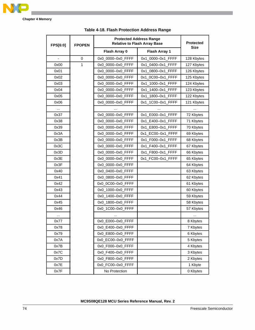
Chapter 4 Memory
Table 4-18. Flash Protection Address Range
FPS[6:0] FPOPEN
Protected Address RangeRelative to Flash Array Base Protected
SizeFlash Array 0 Flash Array 1
- 0 0x0_0000–0x0_FFFF 0x1_0000–0x1_FFFF 128 Kbytes
0x00 1 0x0_0000–0x0_FFFF 0x1_0400–0x1_FFFF 127 Kbytes
0x01 0x0_0000–0x0_FFFF 0x1_0800–0x1_FFFF 126 Kbytes
0x02 0x0_0000–0x0_FFFF 0x1_0C00–0x1_FFFF 125 Kbytes
0x03 0x0_0000–0x0_FFFF 0x1_1000–0x1_FFFF 124 Kbytes
0x04 0x0_0000–0x0_FFFF 0x1_1400–0x1_FFFF 123 Kbytes
0x05 0x0_0000–0x0_FFFF 0x1_1800–0x1_FFFF 122 Kbytes
0x06 0x0_0000–0x0_FFFF 0x1_1C00–0x1_FFFF 121 Kbytes
... ... ... ...
0x37 0x0_0000–0x0_FFFF 0x1_E000–0x1_FFFF 72 Kbytes
0x38 0x0_0000–0x0_FFFF 0x1_E400–0x1_FFFF 71 Kbytes
0x39 0x0_0000–0x0_FFFF 0x1_E800–0x1_FFFF 70 Kbytes
0x3A 0x0_0000–0x0_FFFF 0x1_EC00–0x1_FFFF 69 Kbytes
0x3B 0x0_0000–0x0_FFFF 0x1_F000–0x1_FFFF 68 Kbytes
0x3C 0x0_0000–0x0_FFFF 0x1_F400–0x1_FFFF 67 Kbytes
0x3D 0x0_0000–0x0_FFFF 0x1_F800–0x1_FFFF 66 Kbytes
0x3E 0x0_0000–0x0_FFFF 0x1_FC00–0x1_FFFF 65 Kbytes
0x3F 0x0_0000–0x0_FFFF 64 Kbytes
0x40 0x0_0400–0x0_FFFF 63 Kbytes
0x41 0x0_0800–0x0_FFFF 62 Kbytes
0x42 0x0_0C00–0x0_FFFF 61 Kbytes
0x43 0x0_1000–0x0_FFFF 60 Kbytes
0x44 0x0_1400–0x0_FFFF 59 Kbytes
0x45 0x0_1800–0x0_FFFF 58 Kbytes
0x46 0x0_1C00–0x0_FFFF 57 Kbytes
... ... ...
0x77 0x0_E000–0x0_FFFF 8 Kbytes
0x78 0x0_E400–0x0_FFFF 7 Kbytes
0x79 0x0_E800–0x0_FFFF 6 Kbytes
0x7A 0x0_EC00–0x0_FFFF 5 Kbytes
0x7B 0x0_F000–0x0_FFFF 4 Kbytes
0x7C 0x0_F400–0x0_FFFF 3 Kbytes
0x7D 0x0_F800–0x0_FFFF 2 Kbytes
0x7E 0x0_FC00–0x0_FFFF 1 Kbyte
0x7F No Protection 0 Kbytes
MC9S08QE128 MCU Series Reference Manual, Rev. 2
74 Freescale Semiconductor

Chapter 4 Memory
4.6.2.5 Flash Status Register (FSTAT)
The FSTAT register defines the operational status of the flash module.
FCCF, FPVIOL, and FACCERR are readable and writable, FCCF and FBLANK are readable and not
writable, remaining bits read 0 and are not writable.
7 6 5 4 3 2 1 0
RFCBEF
FCCFFPVIOL FACCERR
0 FBLANK 0 0
W
Reset 1 1 0 0 0 0 0 0
= Unimplemented or Reserved
Figure 4-14. Flash Status Register (FSTAT)
Table 4-19. FSTAT Field Descriptions
Field Description
7FCBEF
Flash Command Buffer Empty Flag — The FCBEF flag indicates that the command buffer is empty so that anew command write sequence can be started when performing burst programming. Writing a 0 to the FCBEFflag has no effect on FCBEF. Writing a 0 to FCBEF after writing an aligned address to the flash array memory,but before FCBEF is cleared, will abort a command write sequence and cause the FACCERR flag to be set.Writing a 0 to FCBEF outside of a command write sequence will not set the FACCERR flag. The FCBEF flag iscleared by writing a 1 to FCBEF.0 Command buffers are full.1 Command buffers are ready to accept a new command.
6FCCF
Flash Command Complete Interrupt Flag — The FCCF flag indicates that there are no more commandspending. The FCCF flag is cleared when FCBEF is cleared and sets automatically upon completion of all activeand pending commands. The FCCF flag does not set when an active program command completes and apending burst program command is fetched from the command buffer. Writing to the FCCF flag has no effect onFCCF.0 Command in progress.1 All commands are completed.
5FPVIOL
Flash Protection Violation Flag —The FPVIOL flag indicates an attempt was made to program or erase anaddress in a protected area of the flash memory or flash IFR during a command write sequence. Writing a 0 tothe FPVIOL flag has no effect on FPVIOL. The FPVIOL flag is cleared by writing a 1 to FPVIOL. While FPVIOLis set, it is not possible to launch a command or start a command write sequence.0 No protection violation detected.1 Protection violation has occurred.
MC9S08QE128 MCU Series Reference Manual, Rev. 2
Freescale Semiconductor 75

Chapter 4 Memory
4.6.2.6 Flash Command Register (FCMD)
The FCMD register is the flash command register.
All FCMD bits are readable and writable during a command write sequence while bit 7 reads 0 and is notwritable.
4FACCERR
Flash Access Error Flag — The FACCERR flag indicates an illegal access has occurred to the flash memoryor flash IFR caused by either a violation of the command write sequence (see Section 4.6.3.1.2, “CommandWrite Sequence”), issuing an illegal flash command (see Table 4-21), or the execution of a CPU STOP instructionwhile a command is executing (FCCF = 0). Writing a 0 to the FACCERR flag has no effect on FACCERR. TheFACCERR flag is cleared by writing a 1 to FACCERR.While FACCERR is set, it is not possible to launch acommand or start a command write sequence.0 No access error detected.1 Access error has occurred.
2FBLANK
Flash Flag Indicating the Erase Verify Operation Status — When the FCCF flag is set after completion of anerase verify command, the FBLANK flag indicates the result of the erase verify operation. The FBLANK flag iscleared by the flash module when FCBEF is cleared as part of a new valid command write sequence. Writing tothe FBLANK flag has no effect on FBLANK.0 Flash block verified as not erased.1 Flash block verified as erased.
7 6 5 4 3 2 1 0
R 0FCMD
W
Reset 0 0 0 0 0 0 0 0
= Unimplemented or Reserved
Figure 4-15. Flash Command Register (FCMD)
Table 4-20. FCMD Field Descriptions
Field Description
6:0FCMD[6:0]
Flash Command — Valid flash commands are shown in Table 4-21. Writing any command other than thoselisted in Table 4-21 sets the FACCERR flag in the FSTAT register.
Table 4-21. Valid Flash Command List
FCMD[6:0] NVM Command
0x05 Erase Verify
0x20 Program
0x25 Burst Program
0x40 Sector Erase
0x41 Mass Erase
Table 4-19. FSTAT Field Descriptions
Field Description
MC9S08QE128 MCU Series Reference Manual, Rev. 2
76 Freescale Semiconductor

Chapter 4 Memory
4.6.3 Functional Description
4.6.3.1 Flash Command Operations
Flash command operations are used to execute program, erase, and erase verify algorithms described inthis section. The program and erase algorithms are controlled by the flash memory controller whose timebase, FCLK, is derived from the bus clock via a programmable divider.
The next sections describe:
1. How to write the FCDIV register to set FCLK
2. Command write sequences to program, erase, and erase verify operations on the flash memory
3. Valid flash commands
4. Effects resulting from illegal flash command write sequences or aborting flash operations
4.6.3.1.1 Writing the FCDIV Register
Prior to issuing any flash command after a reset, the user is required to write the FCDIV register to dividethe bus clock down to within the 150 kHz to 200 kHz range. This register can be written only once, sonormally this write is done during reset initialization. FCDIV cannot be written if the access error flag,FACCERR in FSTAT, is set. The user must ensure that FACCERR is not set before writing to the FCDIVregister. One period of the resulting clock (1/fFCLK) is used by the command processor to time programand erase pulses. An integer number of these timing pulses are used by the command processor to completea program or erase command.
Table 4-22 shows program and erase times. The bus clock frequency and FCDIV determine the frequencyof FCLK (fFCLK). The time for one cycle of FCLK is tFCLK = 1/fFCLK. The times are shown as a numberof cycles of FCLK and as an absolute time for the case where tFCLK = 5 μs. Program and erase timesshown include overhead for the command state machine and enabling and disabling of program and erasevoltages.
NOTEProgram and erase command execution time will increase proportionallywith the period of FCLK. Programming or erasing the flash memory withFCLK < 150 kHz should be avoided. Setting FCDIV to a value such thatFCLK < 150 kHz can destroy the flash memory due to overstress. SettingFCDIV to a value such that FCLK > 200 kHz can result in incompleteprogramming or erasure of the flash memory cells.
Table 4-22. Program and Erase Times
Parameter Cycles of FCLK Time if FCLK = 200 kHz
Byte program 9 45 μs
Byte program (burst) 4 20 μs1
1 Excluding start/end overhead
Page erase 4000 20 ms
Mass erase 20,000 100 ms
MC9S08QE128 MCU Series Reference Manual, Rev. 2
Freescale Semiconductor 77
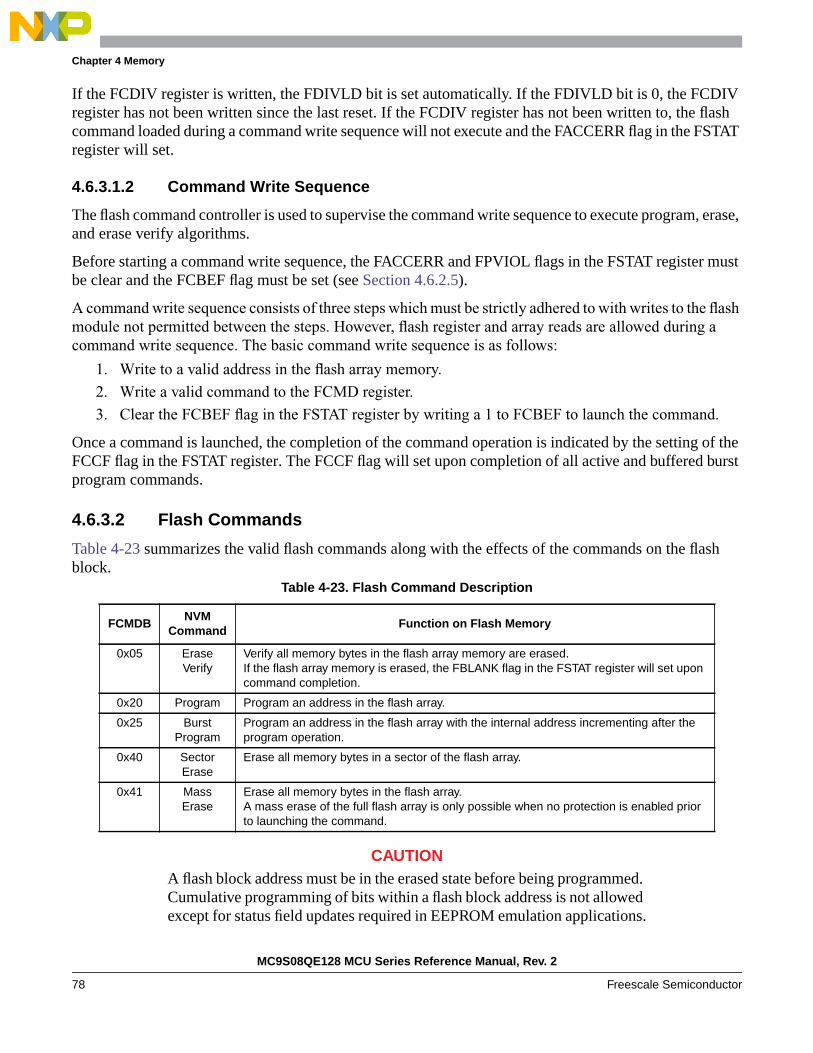
Chapter 4 Memory
If the FCDIV register is written, the FDIVLD bit is set automatically. If the FDIVLD bit is 0, the FCDIVregister has not been written since the last reset. If the FCDIV register has not been written to, the flashcommand loaded during a command write sequence will not execute and the FACCERR flag in the FSTATregister will set.
4.6.3.1.2 Command Write Sequence
The flash command controller is used to supervise the command write sequence to execute program, erase,and erase verify algorithms.
Before starting a command write sequence, the FACCERR and FPVIOL flags in the FSTAT register mustbe clear and the FCBEF flag must be set (see Section 4.6.2.5).
A command write sequence consists of three steps which must be strictly adhered to with writes to the flashmodule not permitted between the steps. However, flash register and array reads are allowed during acommand write sequence. The basic command write sequence is as follows:
1. Write to a valid address in the flash array memory.
2. Write a valid command to the FCMD register.
3. Clear the FCBEF flag in the FSTAT register by writing a 1 to FCBEF to launch the command.
Once a command is launched, the completion of the command operation is indicated by the setting of theFCCF flag in the FSTAT register. The FCCF flag will set upon completion of all active and buffered burstprogram commands.
4.6.3.2 Flash Commands
Table 4-23 summarizes the valid flash commands along with the effects of the commands on the flashblock.
CAUTIONA flash block address must be in the erased state before being programmed.Cumulative programming of bits within a flash block address is not allowedexcept for status field updates required in EEPROM emulation applications.
Table 4-23. Flash Command Description
FCMDBNVM
CommandFunction on Flash Memory
0x05 EraseVerify
Verify all memory bytes in the flash array memory are erased.If the flash array memory is erased, the FBLANK flag in the FSTAT register will set uponcommand completion.
0x20 Program Program an address in the flash array.
0x25 BurstProgram
Program an address in the flash array with the internal address incrementing after theprogram operation.
0x40 SectorErase
Erase all memory bytes in a sector of the flash array.
0x41 MassErase
Erase all memory bytes in the flash array.A mass erase of the full flash array is only possible when no protection is enabled priorto launching the command.
MC9S08QE128 MCU Series Reference Manual, Rev. 2
78 Freescale Semiconductor

Chapter 4 Memory
4.6.3.2.1 Erase Verify Command
The erase verify operation will verify that a flash block is erased.
An example flow to execute the erase verify operation is shown in Figure 4-16. The erase verify commandwrite sequence is as follows:
1. Write to a flash block address to start the command write sequence for the erase verify command.The address and data written will be ignored.
2. Write the erase verify command, 0x05, to the FCMD register.
3. Clear the FCBEF flag in the FSTAT register by writing a 1 to FCBEF to launch the erase verifycommand.
After launching the erase verify command, the FCCF flag in the FSTAT register will set after the operationhas completed. The number of bus cycles required to execute the erase verify operation is equal to thenumber of addresses in the flash array memory plus several bus cycles as measured from the time theFCBEF flag is cleared until the FCCF flag is set. Upon completion of the erase verify operation, theFBLANK flag in the FSTAT register will be set if all addresses in the flash array memory are verified tobe erased. If any address in the flash array memory is not erased, the erase verify operation will terminateand the FBLANK flag in the FSTAT register will remain clear.
MC9S08QE128 MCU Series Reference Manual, Rev. 2
Freescale Semiconductor 79

Chapter 4 Memory
Figure 4-16. Example Erase Verify Command Flow
4.6.3.2.2 Program Command
The program operation will program a previously erased address in the flash memory using an embeddedalgorithm.
An example flow to execute the program operation is shown in Figure 4-17. The program command writesequence is as follows:
1. Write to a flash block address to start the command write sequence for the program command. Thedata written will be programmed to the address written.
2. Write the program command, 0x20, to the FCMD register.
Write: Flash Block Address
Write: FCMD register
Write: FSTAT register
1.
2.
3.
Write: FSTAT registeryes
no
Access Error and
noBit Polling for
Read: FSTAT register
yes
Read: FSTAT register
no
START
yes
FCBEFSet?
Command
FCCFSet?
FACCERR/FPVIOLSet?
noErase Verify
yes
EXITFlash Block
FBLANKSet?
Write: FCDIV register
Read: FCDIV register
yes
noClock Register
FDIVLDSet?
NOTE: FCDIV needs toWrittenCheck
Protection ViolationCheck
Buffer Empty Check
and Dummy Data
Erase Verify Command 0x05
Clear FCBEF 0x80
Clear FACCERR/FPVIOL 0x30
Command CompletionCheck
Status
ErasedFlash BlockNot Erased
EXIT
be set after each reset
MC9S08QE128 MCU Series Reference Manual, Rev. 2
80 Freescale Semiconductor
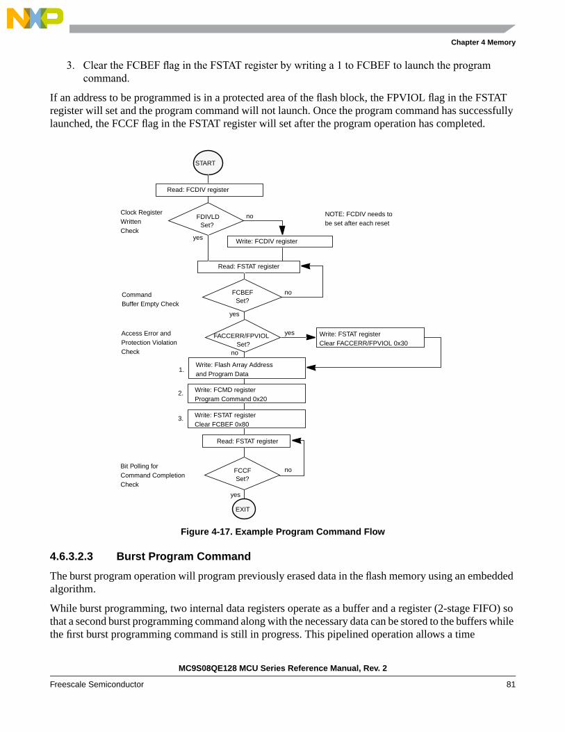
Chapter 4 Memory
3. Clear the FCBEF flag in the FSTAT register by writing a 1 to FCBEF to launch the programcommand.
If an address to be programmed is in a protected area of the flash block, the FPVIOL flag in the FSTATregister will set and the program command will not launch. Once the program command has successfullylaunched, the FCCF flag in the FSTAT register will set after the program operation has completed.
Figure 4-17. Example Program Command Flow
4.6.3.2.3 Burst Program Command
The burst program operation will program previously erased data in the flash memory using an embeddedalgorithm.
While burst programming, two internal data registers operate as a buffer and a register (2-stage FIFO) sothat a second burst programming command along with the necessary data can be stored to the buffers whilethe first burst programming command is still in progress. This pipelined operation allows a time
Write: Flash Array Address
Write: FCMD register
Write: FSTAT register
1.
2.
3.
Write: FSTAT registeryes
no
Access Error and
noBit Polling for
Read: FSTAT register
yes
Read: FSTAT register
no
START
yes
FCBEFSet?
Command
FCCFSet?
FACCERR/FPVIOLSet?
Write: FCDIV register
Read: FCDIV register
yes
noClock Register
FDIVLDSet?
NOTE: FCDIV needs toWrittenCheck
Protection ViolationCheck
Buffer Empty Check
and Program Data
Program Command 0x20
Clear FCBEF 0x80
Clear FACCERR/FPVIOL 0x30
Command CompletionCheck
EXIT
be set after each reset
MC9S08QE128 MCU Series Reference Manual, Rev. 2
Freescale Semiconductor 81

Chapter 4 Memory
optimization when programming more than one consecutive address on a specific row in the flash array asthe high voltage generation can be kept active in between two programming commands.
An example flow to execute the burst program operation is shown in Figure 4-18. The burst programcommand write sequence is as follows:
1. Write to a flash block address to start the command write sequence for the burst program command.The data written will be programmed to the address written.
2. Write the program burst command, 0x25, to the FCMD register.
3. Clear the FCBEF flag in the FSTAT register by writing a 1 to FCBEF to launch the program burstcommand.
4. After the FCBEF flag in the FSTAT register returns to a 1, repeat steps 1 through 3. The addresswritten is ignored but is incremented internally.
The burst program procedure can be used to program an entire flash array even while crossing rowboundaries within the flash array. However, the burst program command cannot cross array boundaries.The array boundary for this MCU occurs between extended addresses 0x0FFFF and 0x10000. At least twoburst commands are required to program the entire 128K of flash memory.
If data to be burst programmed falls within a protected area of the flash array, the FPVIOL flag in theFSTAT register will set and the burst program command will not launch. Once the burst program commandhas successfully launched, the FCCF flag in the FSTAT register will set after the burst program operationhas completed unless a new burst program command write sequence has been buffered. By executing anew burst program command write sequence on sequential addresses after the FCBEF flag in the FSTATregister has been set, greater than 50% faster programming time for the entire flash array can be effectivelyachieved when compared to using the basic program command.
MC9S08QE128 MCU Series Reference Manual, Rev. 2
82 Freescale Semiconductor
Chapter 4 Memory
Figure 4-18. Example Burst Program Command Flow
4.6.3.2.4 Sector Erase Command
The sector erase operation will erase all addresses in a 1 Kbyte sector of flash memory using an embeddedalgorithm.
Write: Flash Array Address
Write: FCMD register
Write: FSTAT register
1.
2.
3.
Write: FSTAT registeryes
no
Access Error and
noBit Polling for
Read: FSTAT register
yes
Read: FSTAT register
no
START
yes
FCBEFSet?
Command
FCCFSet?
FACCERR/FPVIOLSet?
Write: FCDIV register
Read: FCDIV register
yes
noClock Register
FDIVLDSet?
NOTE: FCDIV needs toWrittenCheck
Protection ViolationCheck
Buffer Empty Check
and Program Data
Burst Program Command 0x25
Clear FCBEF 0x80
Clear FACCERR/FPVIOL 0x30
Command CompletionCheck
EXIT
be set after each reset
noBit Polling for
Read: FSTAT register
yes
FCBEFSet?Command Buffer Empty
Check
yesSequential
no
NextAddress?Programming
Decision
MC9S08QE128 MCU Series Reference Manual, Rev. 2
Freescale Semiconductor 83

Chapter 4 Memory
An example flow to execute the sector erase operation is shown in Figure 4-19. The sector erase commandwrite sequence is as follows:
1. Write to a flash block address to start the command write sequence for the sector erase command.The flash address written determines the sector to be erased while global address bits [8:0] and thedata written are ignored.
2. Write the sector erase command, 0x40, to the FCMD register.
3. Clear the FCBEF flag in the FSTAT register by writing a 1 to FCBEF to launch the sector erasecommand.
If a flash sector to be erased is in a protected area of the flash block, the FPVIOL flag in the FSTAT registerwill set and the sector erase command will not launch. Once the sector erase command has successfullylaunched, the FCCF flag in the FSTAT register will set after the sector erase operation has completed.
Figure 4-19. Example Sector Erase Command Flow
Write: Flash Sector Address
Write: FCMD register
Write: FSTAT register
1.
2.
3.
Write: FSTAT registeryes
no
Access Error and
noBit Polling for
Read: FSTAT register
yes
Read: FSTAT register
no
START
yes
FCBEFSet?
Command
FCCFSet?
FACCERR/FPVIOLSet?
Write: FCDIV register
Read: FCDIV register
yes
noClock Register
FDIVLDSet?
NOTE: FCDIV needs toWrittenCheck
Protection ViolationCheck
Buffer Empty Check
and Dummy Data
Sector Erase Command 0x40
Clear FCBEF 0x80
Clear FACCERR/FPVIOL 0x30
Command CompletionCheck
EXIT
be set after each reset
MC9S08QE128 MCU Series Reference Manual, Rev. 2
84 Freescale Semiconductor
Chapter 4 Memory
4.6.3.3 Illegal Flash Operations
4.6.3.3.1 Flash Access Violations
The FACCERR flag will be set during the command write sequence if any of the following illegal stepsare performed, causing the command write sequence to immediately abort:
1. Writing to a flash address before initializing the FCDIV register.
2. Writing to any flash register other than FCMD after writing to a flash address.
3. Writing to a second flash address in the same command write sequence.
4. Writing an invalid command to the FCMD register unless the address written was in a protectedarea of the flash array.
5. Writing a command other than burst program while FCBEF is set and FCCF is clear.
6. When security is enabled, writing a command other than mass erase to the FCMD register whenthe write originates from a non-secure memory location or from the background debug mode.
7. Writing to a flash address after writing to the FCMD register.
8. Writing to any flash register other than FSTAT (to clear FCBEF) after writing to the FCMD register.
9. Writing a 0 to the FCBEF flag in the FSTAT register to abort a command write sequence.
The FACCERR flag will also be set if the MCU enters stop mode while a program or erase operation isactive. The operation is aborted immediately and, if burst programming, any pending burst programcommand is purged (see Section 4.6.4.2, “Stop Mode”).
The FACCERR flag will not be set if any flash register is read during a valid command write sequence.
If the flash memory is read during execution of an algorithm (FCCF = 0), the read operation will returninvalid data and the FACCERR flag will not be set.
If the FACCERR flag is set in the FSTAT register, the user must clear the FACCERR flag before startinganother command write sequence (see Section 4.6.2.5, “Flash Status Register (FSTAT)”).
4.6.3.3.2 Flash Protection Violations
The FPVIOL flag will be set after the command is written to the FCMD register during a command writesequence if any of the following illegal operations are attempted, causing the command write sequence toimmediately abort:
1. Writing the program command if the address written in the command write sequence was in aprotected area of the flash array.
2. Writing the sector erase command if the address written in the command write sequence was in aprotected area of the flash array.
3. Writing the mass erase command while any flash protection is enabled.
4. Writing an invalid command if the address written in the command write sequence was in aprotected area of the flash array.
If the FPVIOL flag is set in the FSTAT register, the user must clear the FPVIOL flag before starting anothercommand write sequence (see Section 4.6.2.5, “Flash Status Register (FSTAT)”).
MC9S08QE128 MCU Series Reference Manual, Rev. 2
Freescale Semiconductor 85
Chapter 4 Memory
4.6.4 Operating Modes
4.6.4.1 Wait Mode
If a command is active (FCCF = 0) when the MCU enters wait mode, the active command and any bufferedcommand will be completed.
4.6.4.2 Stop Mode
If a command is active (FCCF = 0) when the MCU enters stop mode, the operation will be aborted and, ifthe operation is program or erase, the flash array data being programmed or erased may be corrupted andthe FCCF and FACCERR flags will be set. If active, the high voltage circuitry to the flash array willimmediately be switched off when entering stop mode. Upon exit from stop mode, the FCBEF flag is setand any buffered command will not be launched. The FACCERR flag must be cleared before starting acommand write sequence (see Section 4.6.3.1.2, “Command Write Sequence”).
NOTEAs active commands are immediately aborted when the MCU enters stopmode, it is strongly recommended that the user does not use the STOPinstruction during program or erase operations.
4.6.4.3 Background Debug Mode
In background debug mode (BDM), the FPROT register is writable. If the MCU is unsecured, then all flashcommands listed in Table 4-23 can be executed.
4.6.5 Flash Module Security
The MC9S08QE128 Series includes circuitry to prevent unauthorized access to the contents of flash andRAM memory. When security is engaged, flash and RAM are considered secure resources. Direct-pageregisters, high-page registers, and the background debug controller are considered unsecured resources.Programs executing within secure memory have normal access to any MCU memory locations andresources. Attempts to access a secure memory location with a program executing from an unsecuredmemory space or through the background debug interface are blocked (writes are ignored and reads returnall 0s).
The flash module provides the necessary security information to the MCU. During each reset sequence,the flash module determines the security state of the MCU as defined in Section 4.6.2.2, “Flash OptionsRegister (FOPT and NVOPT)”.
The contents of the flash security byte in NVOPT must be changed directly by programming the NVOPTlocation when the MCU is unsecured and the sector containing NVOPT is unprotected. If NVOPT is leftin a secured state, any reset will cause the MCU to initialize into a secure operating mode.
The on-chip debug module cannot be enabled while the MCU is secure. The separate background debugcontroller can still be used for background memory access commands of unsecured resources.
MC9S08QE128 MCU Series Reference Manual, Rev. 2
86 Freescale Semiconductor

Chapter 4 Memory
4.6.5.1 Unsecuring the MCU using Backdoor Key Access
The MCU may be unsecured by using the backdoor key access feature which requires knowledge of thecontents of the backdoor keys (NVBACKKEY through NVBACKKEY+7, see Table 4-4 for specificaddresses). If the KEYEN[1:0] bits are in the enabled state (see Section 4.6.2.2) and the KEYACC bit isset, a write to a backdoor key address in the flash memory triggers a comparison between the written dataand the backdoor key data stored in the flash memory. If all backdoor keys are written to the correctaddresses in the correct order and the data matches the backdoor keys stored in the flash memory, the MCUwill be unsecured. The data must be written to the backdoor keys sequentially. Values 0x0000 and 0xFFFFare not permitted as backdoor keys. While the KEYACC bit is set, reads of the flash memory will returninvalid data.
The user code stored in the flash memory must have a method of receiving the backdoor keys from anexternal stimulus. This external stimulus would typically be through one of the on-chip serial ports.
If the KEYEN[1:0] bits are in the enabled state (see Section 4.6.2.2), the MCU can be unsecured by thebackdoor key access sequence described below:
1. Set the KEYACC bit in the flash configuration register (FCNFG).
2. Sequentially write the correct eight 8-bit bytes to the flash addresses containing the backdoor keys.
3. Clear the KEYACC bit. Depending on the user code used to write the backdoor keys, a wait cycle(NOP) may be required before clearing the KEYACC bit.
4. If all data written match the backdoor keys, the MCU is unsecured and the SEC[1:0] bits in theFOPT register are forced to the unsecure state of 1:0.
The backdoor key access sequence is monitored by an internal security state machine. An illegal operationduring the backdoor key access sequence will cause the security state machine to lock, leaving the MCUin the secured state. A reset of the MCU will cause the security state machine to exit the lock state andallow a new backdoor key access sequence to be attempted. The following operations during the backdoorkey access sequence will lock the security state machine:
1. If any of the keys written does not match the backdoor keys programmed in the flash array.
2. If the keys are written in the wrong sequence.
3. If more keys than are required are written.
4. If any of the keys written are all 0s or all 1s.
5. If the KEYACC bit does not remain set while the keys are written.
6. If any of the keys are written on successive MCU clock cycles.
7. Executing a STOP instruction while the KEYACC bit is set.
After the backdoor keys have been correctly matched, the MCU will be unsecured. After the MCU isunsecured, the flash security byte can be programmed to the unsecure state, if desired.
In the unsecure state, the user has full control of the contents of the backdoor keys by programming theassociated addresses in NVBACKKEY through NVBACKKEY+7.
The security as defined in the flash security byte is not changed by using the backdoor key access sequenceto unsecure. The stored backdoor keys are unaffected by the backdoor key access sequence. After the nextreset of the MCU, the security state of the flash module is determined by the flash security byte. The
MC9S08QE128 MCU Series Reference Manual, Rev. 2
Freescale Semiconductor 87

Chapter 4 Memory
backdoor key access sequence has no effect on the program and erase protections defined in the flashprotection register (FPROT).
It is not possible to unsecure the MCU in special mode by using the backdoor key access sequence inbackground debug mode (BDM).
4.6.6 Resets
If a reset occurs while any flash command is in progress, that command will be immediately aborted. Thestate of the flash array address being programmed or the sector/block being erased is not guaranteed.
MC9S08QE128 MCU Series Reference Manual, Rev. 2
88 Freescale Semiconductor

Chapter 5Resets, Interrupts, and General System Control
5.1 IntroductionThis section discusses basic reset and interrupt mechanisms and the various sources of reset and interruptin the MC9S08QE128 Series. Some interrupt sources from peripheral modules are discussed in greaterdetail within other sections of this reference manual. This section gathers basic information about all resetand interrupt sources in one place for easy reference. A few reset and interrupt sources, including thecomputer operating properly (COP) watchdog are not part of on-chip peripheral systems with their ownchapters.
5.2 FeaturesReset and interrupt features include:
• Multiple sources of reset for flexible system configuration and reliable operation• Reset status register (SRS) to indicate source of most recent reset• Separate interrupt vector for most modules (reduces polling overhead) (see Table 5-2)
5.3 MCU ResetResetting the MCU provides a way to start processing from a known set of initial conditions. During reset,most control and status registers are forced to initial values and the program counter is loaded from thereset vector (0xFFFE:0xFFFF). On-chip peripheral modules are disabled and I/O pins are initiallyconfigured as general-purpose high-impedance inputs with pull-up devices disabled. The I bit in thecondition code register (CCR) is set to block maskable interrupts so the user program has a chance toinitialize the stack pointer (SP) and system control settings. SP is forced to 0x00FF at reset.
The MC9S08QE128 Series has the following sources for reset:
• Power-on reset (POR)• External pin reset (PIN)• Computer operating properly (COP) timer• Illegal opcode detect (ILOP)• Low-voltage detect (LVD)• Background debug forced reset
Each of these sources, with the exception of the background debug forced reset, has an associated bit inthe system reset status register (SRS).
MC9S08QE128 MCU Series Reference Manual, Rev. 2
Freescale Semiconductor 89

Chapter 5 Resets, Interrupts, and General System Control
5.4 Computer Operating Properly (COP) WatchdogThe COP watchdog is intended to force a system reset when the application software fails to execute asexpected. To prevent a system reset from the COP timer (when it is enabled), application software mustreset the COP counter periodically. If the application program gets lost and fails to reset the COP counterbefore it times out, a system reset is generated to force the system back to a known starting point.
After any reset, the COPE becomes set in SOPT1 enabling the COP watchdog (see Section 5.8.4, “SystemOptions Register 1 (SOPT1),” for additional information). If the COP watchdog is not used in anapplication, it can be disabled by clearing COPE. The COP counter is reset by writing any value to theaddress of SRS. This write does not affect the data in the read-only SRS. Instead, the act of writing to thisaddress is decoded and sends a reset signal to the COP counter.
The COPCLKS bit in SOPT2 (see Section 5.8.5, “System Options Register 2 (SOPT2),” for additionalinformation) selects the clock source used for the COP timer. The clock source options are either the busclock or an internal 1-kHz clock source. With each clock source, there is an associated short and longtime-out controlled by COPT in SOPT1. Table 5-1 summaries the control functions of the COPCLKS andCOPT bits. The COP watchdog defaults to operation from the 1-kHz clock source and the associated longtime-out (28 cycles).
Even if the application will use the reset default settings of COPE, COPCLKS, and COPT, the user mustwrite to the write-once SOPT1 and SOPT2 registers during reset initialization to lock in the settings. Thatway, they cannot be changed accidentally if the application program gets lost. The initial writes to SOPT1and SOPT2 will reset the COP counter.
The write to SRS that services (clears) the COP counter must not be placed in an interrupt service routine(ISR) because the ISR could continue to be executed periodically even if the main application programfails.
In background debug mode, the COP counter will not increment.
When the bus clock source is selected, the COP counter does not increment while the system is in stopmode. The COP counter resumes as soon as the MCU exits stop mode.
Table 5-1. COP Configuration Options
Control BitsClock Source COP Overflow Count
COPCLKS COPT
0 0 ~1 kHz 25 cycles (32 ms)1
1 Values are shown in this column based on tLPO = 1 ms. See tLPO in the data sheet for thetolerance of this value.
0 1 ~1 kHz 28 cycles (256 ms)1
1 0 Bus 213 cycles
1 1 Bus 218 cycles
MC9S08QE128 MCU Series Reference Manual, Rev. 2
90 Freescale Semiconductor
Chapter 5 Resets, Interrupts, and General System Control
When the 1-kHz clock source is selected, the COP counter is re-initialized to zero upon entry to stop mode.The COP counter begins from zero after the MCU exits stop mode.
5.5 InterruptsInterrupts provide a way to save the current CPU status and registers, execute an interrupt service routine(ISR), and then restore the CPU status so processing resumes where it left off before the interrupt. Otherthan the software interrupt (SWI), which is a program instruction, interrupts are caused by hardware eventssuch as an edge on the IRQ pin or a timer-overflow event. The debug module can also generate an SWIunder certain circumstances.
If an event occurs in an enabled interrupt source, an associated read-only status flag will become set. TheCPU will not respond unless the local interrupt enable is a 1 to enable the interrupt and the I bit in the CCRis 0 to allow interrupts. The global interrupt mask (I bit) in the CCR is initially set after reset whichprevents all maskable interrupt sources. The user program initializes the stack pointer and performs othersystem setup before clearing the I bit to allow the CPU to respond to interrupts.
When the CPU receives a qualified interrupt request, it completes the current instruction before respondingto the interrupt. The interrupt sequence obeys the same cycle-by-cycle sequence as the SWI instruction andconsists of:
• Saving the CPU registers on the stack
• Setting the I bit in the CCR to mask further interrupts
• Fetching the interrupt vector for the highest-priority interrupt that is currently pending
• Filling the instruction queue with the first three bytes of program information starting from theaddress fetched from the interrupt vector locations
While the CPU is responding to the interrupt, the I bit is automatically set to avoid the possibility of anotherinterrupt interrupting the ISR itself (this is called nesting of interrupts). Normally, the I bit is restored to 0when the CCR is restored from the value stacked on entry to the ISR. In rare cases, the I bit can be clearedinside an ISR (after clearing the status flag that generated the interrupt) so that other interrupts can beserviced without waiting for the first service routine to finish. This practice is not recommended for anyoneother than the most experienced programmers because it can lead to subtle program errors that are difficultto debug.
NOTEIn order for the ISR to be available in the memory map regardless of thePPAGE value, ISRs should be located in pages 0, 1, or 3.
The interrupt service routine ends with a return-from-interrupt (RTI) instruction which restores the CCR,A, X, and PC registers to their pre-interrupt values by reading the previously saved information from thestack.
NOTEFor compatibility with M68HC08 devices, the H register is notautomatically saved and restored. It is good programming practice to pushH onto the stack at the start of the interrupt service routine (ISR) and restoreit immediately before the RTI that is used to return from the ISR.
MC9S08QE128 MCU Series Reference Manual, Rev. 2
Freescale Semiconductor 91

Chapter 5 Resets, Interrupts, and General System Control
If more than one interrupt is pending when the I bit is cleared, the highest priority source is serviced first(see Table 5-2).
5.5.1 Interrupt Stack Frame
Figure 5-1 shows the contents and organization of a stack frame. Before the interrupt, the stack pointer(SP) points at the next available byte location on the stack. The current values of CPU registers are storedon the stack starting with the low-order byte of the program counter (PCL) and ending with the CCR. Afterstacking, the SP points at the next available location on the stack which is the address that is one less thanthe address where the CCR was saved. The PC value that is stacked is the address of the instruction in themain program that would have executed next if the interrupt had not occurred.
Figure 5-1. Interrupt Stack Frame
When an RTI instruction is executed, these values are recovered from the stack in reverse order. As part ofthe RTI sequence, the CPU fills the instruction pipeline by reading three bytes of program information,starting from the PC address recovered from the stack.
The status flag corresponding to the interrupt source must be acknowledged (cleared) before returningfrom the ISR. Typically, the flag is cleared at the beginning of the ISR so that if another interrupt isgenerated by this same source, it will be registered so it can be serviced after completion of the current ISR.
5.5.2 External Interrupt Request (IRQ) Pin
External interrupts are managed by the IRQ status and control register, IRQSC. When the IRQ function isenabled, synchronous logic monitors the pin for edge-only or edge-and-level events. When the MCU is instop mode and system clocks are shut down, a separate asynchronous path is used so the IRQ pin (ifenabled) can wake the MCU.
CONDITION CODE REGISTER
ACCUMULATOR
INDEX REGISTER (LOW BYTE X)
PROGRAM COUNTER HIGH
* High byte (H) of index register is not automatically stacked.
*
PROGRAM COUNTER LOW
7 0
UNSTACKINGORDER
STACKINGORDER
5
4
3
2
1
1
2
3
4
5
TOWARD LOWER ADDRESSES
TOWARD HIGHER ADDRESSES
SP BEFORE
SP AFTERINTERRUPT STACKING
THE INTERRUPT
MC9S08QE128 MCU Series Reference Manual, Rev. 2
92 Freescale Semiconductor
Chapter 5 Resets, Interrupts, and General System Control
5.5.2.1 Pin Configuration Options
The IRQ pin enable (IRQPE) control bit in IRQSC must be 1 in order for the IRQ pin to act as the interruptrequest (IRQ) input. As an IRQ input, the user can choose the polarity of edges or levels detected(IRQEDG), whether the pin detects edges-only or edges and levels (IRQMOD), and whether an eventcauses an interrupt or only sets the IRQF flag which can be polled by software (IRQIE).
The IRQ pin, when enabled, defaults to use an internal pull device (IRQPDD = 0), configured as a pull-upor pull-down depending on the polarity chosen. If the user desires to use an external pull-up or pull-down,the IRQPDD can be written to a 1 to turn off the internal device.
BIH and BIL instructions may be used to detect the level on the IRQ pin when the pin is configured to actas the IRQ input.
NOTEThis pin does not contain a clamp diode to VDD and should not be drivenabove VDD.
NOTEThe voltage measured on the internally pulled up RESET pin will not bepulled to VDD. The internal gates connected to this pin are pulled to VDD.The RESET pullup should not be used to pullup components external to theMCU.
5.5.2.2 Edge and Level Sensitivity
The IRQMOD control bit reconfigures the detection logic so it detects edge events and pin levels. In theedge and level detection mode, the IRQF status flag becomes set when an edge is detected (when the IRQpin changes from the deasserted to the asserted level), but the flag is continuously set (and cannot becleared) as long as the IRQ pin remains at the asserted level.
5.5.2.3 External Interrupt Initialization
When the IRQ pin is first enabled, it is possible to get a false interrupt flag. To prevent a false interruptrequest during IRQ initialization, the user should do the following:
1. Mask interrupts by clearing IRQIE in IRQSC.
2. Select the pin polarity by setting the appropriate IRQEDG bits in IRQSC.
3. If using internal pull-up/pull-down device, clear the IRQPDD bit in IRQSC.
4. Enable the IRQ pin by setting the appropriate IRQPE bit in IRQSC.
5. Write to IRQACK in IRQSC to clear any false interrupts.
6. Set IRQIE in IRQSC to enable interrupts.
5.5.3 Interrupt Vectors, Sources, and Local Masks
Table 5-2 provides a summary of all interrupt sources. Higher-priority sources are located toward thebottom of the table. The high-order byte of the address for the interrupt service routine is located at the
MC9S08QE128 MCU Series Reference Manual, Rev. 2
Freescale Semiconductor 93

Chapter 5 Resets, Interrupts, and General System Control
first address in the vector address column, and the low-order byte of the address for the interrupt serviceroutine is located at the next higher address.
When an interrupt condition occurs, an associated flag bit becomes set. If the associated local interruptenable is 1, an interrupt request is sent to the CPU. Within the CPU, if the global interrupt mask (I bit inthe CCR) is 0, the CPU will finish the current instruction; stack the PCL, PCH, X, A, and CCR CPUregisters; set the I bit; and then fetch the interrupt vector for the highest priority pending interrupt.Processing then continues in the interrupt service routine.
MC9S08QE128 MCU Series Reference Manual, Rev. 2
94 Freescale Semiconductor

Chapter 5 Resets, Interrupts, and General System Control
Table 5-2. Vector Summary
VectorPriority
VectorNumber
Address(High/Low)
VectorName
Module Source Enable Description
Lowest
Highest
31 0xFFC0/0xFFC1 Vtpm3ovf TPM3 TOF TOIE TPM3 overflow30 0xFFC2/0xFFC3 Vtpm3ch5 TPM3 CH5F CH5IE TPM3 channel 529 0xFFC4/0xFFC5 Vtpm3ch4 TPM3 CH4F CH4IE TPM3 channel 428 0xFFC6/0xFFC7 Vtpm3ch3 TPM3 CH3F CH3IE TPM3 channel 327 0xFFC8/0xFFC9 Vtpm3ch2 TPM3 CH2F CH2IE TPM3 channel 226 0xFFCA/0xFFCB Vtpm3ch1 TPM3 CH1F CH1IE TPM3 channel 125 0xFFCC/0xFFCD Vtpm3ch0 TPM3 CH0F CH0IE TPM3 channel 024 0xFFCE/0xFFCF Vrtc RTC RTIF RTIE Real-time interrupt23 0xFFD0/0xFFD1 Vsci2tx SCI2 TDRE, TC TIE, TCIE SCI2 transmit22 0xFFD2/0xFFD3 Vsci2rx SCI2 IDLE, LBKDIF,
RDRF, RXEDGIFILIE, LBKDIE, RIE,
RXEDGIESCI2 receive
21 0xFFD4/0xFFD5 Vsci2err SCI2 OR, NFFE, PF
ORIE, NFIE,FEIE, PFIE
SCI2 error
20 0xFFD6/0xFFD7 Vacmpx ACMPx1
1 ACMP1 and ACMP2 share this vector, if both modules are enabled user should poll each flag to determine pending interrupt.
ACF ACIE Analog comparator x19 0xFFD8/0xFFD9 Vadc ADC COCO AIEN ADC18 0xFFDA/0xFFDB Vkeyboard KBIx2
2 KBI1 and KBI2 share this vector, if both modules are enabled user should poll each flag to determine pending interrupt.
KBF KBIE Keyboard x pins17 0xFFDC/0xFFDD Viicx IICx3
3 IIC1 and IIC2 share this vector, if both modules are enabled user should poll each flag to determine pending interrupt.
IICIS IICIE IICx control16 0xFFDE/0xFFDF Vsci1tx SCI1 TDRE, TC TIE, TCIE SCI1 transmit15 0xFFE0/0xFFE1 Vsci1rx SCI1 IDLE, LBKDIF,
RDRF, RXEDGIFILIE, LBKDIE, RIE,
RXEDGIESCI1 receive
14 0xFFE2/0xFFE3 Vsci1err SCI1 OR, NF,FE, PF
ORIE, NFIE,FEIE, PFIE
SCI1 error
13 0xFFE4/0xFFE5 Vspi1 SPI1 SPIF, MODF,SPTEF
SPIE, SPIE, SPTIE SPI1
12 0xFFE6/0xFFE7 Vspi2 SPI2 SPIF, MODF,SPTEF
SPIE, SPIE, SPTIE SPI2
11 0xFFE8/0xFFE9 Vtpm2ovf TPM2 TOF TOIE TPM2 overflow10 0xFFEA/0xFFEB Vtpm2ch2 TPM2 CH2F CH2IE TPM2 channel 29 0xFFEC/0xFFED Vtpm2ch1 TPM2 CH1F CH1IE TPM2 channel 18 0xFFEE/0xFFEF Vtpm2ch0 TPM2 CH0F CH0IE TPM2 channel 07 0xFFF0/0xFFF1 Vtpm1ovf TPM1 TOF TOIE TPM1 overflow6 0xFFF2/0xFFF3 Vtpm1ch2 TPM1 CH2F CH2IE TPM1 channel 25 0xFFF4/0xFFF5 Vtpm1ch1 TPM1 CH1F CH1IE TPM1 channel 14 0xFFF6/0xFFF7 Vtpm1ch0 TPM1 CH0F CH0IE TPM1 channel 03 0xFFF8/0xFFF9 Vlvd System
controlLVDF, LVWF LVDIE, LVWIE Low-voltage detect,
Low-voltage warning2 0xFFFA/0xFFFB Virq IRQ IRQF IRQIE IRQ pin1 0xFFFC/0xFFFD Vswi Core SWI Instruction — Software interrupt0 0xFFFE/0xFFFF Vreset System
controlCOP,LVD,
RESET pin,Illegal opcode,
COPELVDRE
——
Watchdog timerLow-voltage detect
External pinIllegal opcode
MC9S08QE128 MCU Series Reference Manual, Rev. 2
Freescale Semiconductor 95
Chapter 5 Resets, Interrupts, and General System Control
5.6 Low-Voltage Detect (LVD) SystemThe MC9S08QE128 Series includes a system to protect against low voltage conditions to protect memorycontents and control MCU system states during supply voltage variations. The system is comprised of apower-on reset (POR) circuit and a LVD circuit with a user selectable trip voltage, either high (VLVDH) orlow (VLVDL). The LVD circuit is enabled when LVDE in SPMSC1 is set and the trip voltage is selectedby LVDV in SPMSC3. The LVD is disabled upon entering either of the stop modes unless LVDSE is setin SPMSC1. If LVDSE and LVDE are both set, then the MCU will enter stop3 instead of stop2, and thecurrent consumption in stop3 with the LVD enabled will be greater.
5.6.1 Power-On Reset Operation
When power is initially applied to the MCU, or when the supply voltage drops below the power-on resetrearm voltage level, VPOR, the POR circuit will cause a reset condition. As the supply voltage rises, theLVD circuit will hold the MCU in reset until the supply has risen above the low voltage detection lowthreshold, VLVDL. Both the POR bit and the LVD bit in SRS are set following a POR.
5.6.2 Low-Voltage Detection (LVD) Reset Operation
The LVD can be configured to generate a reset upon detection of a low voltage condition by settingLVDRE to 1. The low voltage detection threshold is determined by the LVDV bit. After an LVD reset hasoccurred, the LVD system will hold the MCU in reset until the supply voltage has risen above the lowvoltage detection threshold. The LVD bit in the SRS register is set following either an LVD reset or POR.
5.6.3 Low-Voltage Detection (LVD) Interrupt Operation
When a low voltage condition is detected and the LVD circuit is configured using SPMSC1 for interruptoperation (LVDE set, LVDIE set, and LVDRE clear), then LVDF in SPMSC1 will be set and an LVDinterrupt request will occur. The LVDF bit is cleared by writing a 1 to the LVDACK bit in SPMSC1.
5.6.4 Low-Voltage Warning (LVW) Interrupt Operation
The LVD system has a low voltage warning flag (LVWF) to indicate to the user that the supply voltage isapproaching, but is above, the LVD voltage. The LVW also has an interrupt associated with it, enabled bysetting the LVWIE bit in the SPMSC3 register. If enabled, an LVW interrupt request will occur when theLVWF is set. LVWF is cleared by writing a 1 to the LVWACK bit in SPMSC3. There are two userselectable trip voltages for the LVW, one high (VLVWH) and one low (VLVWL). The trip voltage is selectedby LVWV in SPMSC3.
5.7 Peripheral Clock GatingThe MC9S08QE128 Series includes a clock gating system to manage the bus clock sources to theindividual peripherals. Using this system, the user can enable or disable the bus clock to each of theperipherals at the clock source, eliminating unnecessary clocks to peripherals which are not in use andthereby reducing the overall run and wait mode currents.
MC9S08QE128 MCU Series Reference Manual, Rev. 2
96 Freescale Semiconductor

Chapter 5 Resets, Interrupts, and General System Control
Out of reset, all peripheral clocks will be enabled. For lowest possible run or wait currents, user softwareshould disable the clock source to any peripheral not in use. The actual clock will be enabled or disabledimmediately following the write to the Clock Gating Control registers (SCGC1 and SCGC2). Anyperipheral with a gated clock can not be used unless its clock is enabled. Writing to the registers of aperipheral with a disabled clock has no effect.
NOTEUser software should disable the peripheral before disabling the clocks tothe peripheral. When clocks are re-enabled to a peripheral, the peripheralregisters need to be re-initialized by user software.
In stop modes, the bus clock is disabled for all gated peripherals, regardless of the settings in SCGC1 andSCGC2.
MC9S08QE128 MCU Series Reference Manual, Rev. 2
Freescale Semiconductor 97

Chapter 5 Resets, Interrupts, and General System Control
5.8 Reset, Interrupt, and System Control Registers and Control BitsOne 8-bit register in the direct page register space and eight 8-bit registers in the high-page register spaceare related to reset and interrupt systems.
Refer to Table 4-2 and Table 4-3 in Chapter 4, “Memory,” of this data sheet for the absolute addressassignments for all registers. This section refers to registers and control bits only by their names. AFreescale-provided equate or header file is used to translate these names into the appropriate absoluteaddresses.
Some control bits in the SOPT1 and SPMSC2 registers are related to modes of operation. Although briefdescriptions of these bits are provided here, the related functions are discussed in greater detail inChapter 3, “Modes of Operation.”
5.8.1 Interrupt Pin Request Status and Control Register (IRQSC)
This direct page register includes status and control bits which are used to configure the IRQ function,report status, and acknowledge IRQ events.
7 6 5 4 3 2 1 0
R 0IRQPDD IRQEDG IRQPE
IRQF 0IRQIE IRQMOD
W IRQACK
Reset 0 0 0 0 0 0 0 0
= Unimplemented or Reserved
Figure 5-2. Interrupt Request Status and Control Register (IRQSC)
Table 5-3. IRQSC Register Field Descriptions
Field Description
6IRQPDD
Interrupt Request (IRQ) Pull Device Disable— This read/write control bit is used to disable the internalpull-up/pull-down device when the IRQ pin is enabled (IRQPE = 1) allowing for an external device to be used.0 IRQ pull device enabled if IRQPE = 1.1 IRQ pull device disabled if IRQPE = 1.
5IRQEDG
Interrupt Request (IRQ) Edge Select — This read/write control bit is used to select the polarity of edges orlevels on the IRQ pin that cause IRQF to be set. The IRQMOD control bit determines whether the IRQ pin issensitive to both edges and levels or only edges. When IRQEDG = 1 and the internal pull device is enabled, thepull-up device is reconfigured as an optional pull-down device.0 IRQ is falling edge or falling edge/low-level sensitive.1 IRQ is rising edge or rising edge/high-level sensitive.
4IRQPE
IRQ Pin Enable — This read/write control bit enables the IRQ pin function. When this bit is set the IRQ pin canbe used as an interrupt request.0 IRQ pin function is disabled.1 IRQ pin function is enabled.
3IRQF
IRQ Flag — This read-only status bit indicates when an interrupt request event has occurred.0 No IRQ request.1 IRQ event detected.
MC9S08QE128 MCU Series Reference Manual, Rev. 2
98 Freescale Semiconductor
Chapter 5 Resets, Interrupts, and General System Control
5.8.2 System Reset Status Register (SRS)
This high page register includes read-only status flags to indicate the source of the most recent reset. Whena debug host forces reset by writing 1 to BDFR in the SBDFR register, none of the status bits in SRS willbe set. Writing any value to this register address clears the COP watchdog timer without affecting thecontents of this register. The reset state of these bits depends on what caused the MCU to reset.
Figure 5-3. System Reset Status (SRS)
2IRQACK
IRQ Acknowledge — This write-only bit is used to acknowledge interrupt request events (write 1 to clear IRQF).Writing 0 has no meaning or effect. Reads always return 0. If edge-and-level detection is selected (IRQMOD = 1),IRQF cannot be cleared while the IRQ pin remains at its asserted level.
1IRQIE
IRQ Interrupt Enable — This read/write control bit determines whether IRQ events generate an interruptrequest.0 Interrupt request when IRQF set is disabled (use polling).1 Interrupt requested whenever IRQF = 1.
0IRQMOD
IRQ Detection Mode — This read/write control bit selects either edge-only detection or edge-and-leveldetection. The IRQEDG control bit determines the polarity of edges and levels that are detected as interruptrequest events. See Section 5.5.2.2, “Edge and Level Sensitivity” for more details.0 IRQ event on falling edges or rising edges only.1 IRQ event on falling edges and low levels or on rising edges and high levels.
7 6 5 4 3 2 1 0
R POR PIN COP ILOP 0 0 LVD 0
W Writing any value to SRS address clears COP watchdog timer.
POR: 1 0 0 0 0 0 1 0
LVD: u1
1 u = unaffected
0 0 0 0 0 1 0
Anyotherreset:
0 Note 2
2 Any of these reset sources that are active at the time of reset entry will cause the corresponding bit(s) to be set; bitscorresponding to sources that are not active at the time of reset entry will be cleared.
Note 2 Note2 0 0 0 0
Table 5-3. IRQSC Register Field Descriptions
Field Description
MC9S08QE128 MCU Series Reference Manual, Rev. 2
Freescale Semiconductor 99

Chapter 5 Resets, Interrupts, and General System Control
5.8.3 System Background Debug Force Reset Register (SBDFR)
This high page register contains a single write-only control bit. A serial background command such asWRITE_BYTE must be used to write to SBDFR. Attempts to write this register from a user program areignored. Reads always return 0x00.
Figure 5-4. System Background Debug Force Reset Register (SBDFR)
Table 5-4. SRS Register Field Descriptions
Field Description
7POR
Power-On Reset — Reset was caused by the power-on detection logic. Because the internal supply voltage wasramping up at the time, the low-voltage reset (LVD) status bit is also set to indicate that the reset occurred whilethe internal supply was below the LVD threshold.0 Reset not caused by POR.1 POR caused reset.
6PIN
External Reset Pin — Reset was caused by an active-low level on the external reset pin.0 Reset not caused by external reset pin.1 Reset came from external reset pin.
5COP
Computer Operating Properly (COP) Watchdog — Reset was caused by the COP watchdog timer timing out.This reset source can be blocked by COPE = 0.0 Reset not caused by COP timeout.1 Reset caused by COP timeout.
4ILOP
Illegal Opcode — Reset was caused by an attempt to execute an unimplemented or illegal opcode. The STOPinstruction is considered illegal if stop is disabled by STOPE = 0 in the SOPT register. The BGND instruction isconsidered illegal if active background mode is disabled by ENBDM = 0 in the BDCSC register.0 Reset not caused by an illegal opcode.1 Reset caused by an illegal opcode.
1LVD
Low Voltage Detect — If the LVDRE bit is set and the supply drops below the LVD trip voltage, an LVD reset willoccur. This bit is also set by POR.0 Reset not caused by LVD trip or POR.1 Reset caused by LVD trip or POR.
7 6 5 4 3 2 1 0
R 0 0 0 0 0 0 0 0
W BDFR1
1 BDFR is writable only through serial background debug commands, not from user programs.
Reset: 0 0 0 0 0 0 0 0
= Unimplemented or Reserved
MC9S08QE128 MCU Series Reference Manual, Rev. 2
100 Freescale Semiconductor
Chapter 5 Resets, Interrupts, and General System Control
5.8.4 System Options Register 1 (SOPT1)
This high page register is a write-once register so only the first write after reset is honored. It can be readat any time. Any subsequent attempt to write to SOPT1 (intentionally or unintentionally) is ignored toavoid accidental changes to these sensitive settings. SOPT1 should be written during the user’s resetinitialization program to set the desired controls even if the desired settings are the same as the resetsettings.
Table 5-5. SBDFR Register Field Descriptions
Field Description
0BDFR
Background Debug Force Reset — A serial background command such as WRITE_BYTE can be used to allowan external debug host to force a target system reset. Writing 1 to this bit forces an MCU reset. This bit cannotbe written from a user program.To enter user mode, PTA4/ACMPO/BKGD/MS must be high immediately afterissuing WRITE_BYTE command. To enter BDM, PTA4/ACMPO/BKGD/MS must be low immediately after issuingWRITE_BYTE command. See the data sheet for more information.
7 6 5 4 3 2 1 0
RCOPE COPT STOPE
0 0RSTOPE BKGDPE RSTPE
W
Reset: 1 1 0 0 0 u1
1 u = unaffected
1 u1
POR: 1 1 0 0 0 0 1 0
LVR: 1 1 0 0 0 0 1 0
= Unimplemented or Reserved
Figure 5-5. System Options Register 1 (SOPT1)
Table 5-6. SOPT1 Register Field Descriptions
Field Description
7COPE
COP Watchdog Enable — This write-once bit selects whether the COP watchdog is enabled.0 COP watchdog timer disabled.1 COP watchdog timer enabled (force reset on timeout).
6COPT
COP Watchdog Timeout — This write-once bit selects the timeout period of the COP. COPT along withCOPCLKS in SOPT2 defines the COP timeout period.0 Short timeout period selected.1 Long timeout period selected.
5STOPE
Stop Mode Enable — This write-once bit is used to enable stop mode. If stop mode is disabled and a userprogram attempts to execute a STOP instruction, an illegal opcode reset is forced.0 Stop mode disabled.1 Stop mode enabled.
2RSTOPE
RSTO Pin Enable — This write-once bit when set enables the PTC4/TPM3CH4/RSTO pin to function as RSTO.When clear, the pin functions as one of its alternative functions. This pin defaults to its I/O port function followingan MCU POR.0 PTC4/TPM3CH4/RSTO pin functions as PTC4 or TPM3CH4.1 PTC4/TPM3CH4/RSTO pin functions as RSTO.
MC9S08QE128 MCU Series Reference Manual, Rev. 2
Freescale Semiconductor 101
Chapter 5 Resets, Interrupts, and General System Control
5.8.5 System Options Register 2 (SOPT2)
This high page register contains bits to configure MCU specific features on the MC9S08QE128 Seriesdevices.
1BKGDPE
Background Debug Mode Pin Enable — This write-once bit when set enables the PTA4/ACMPO/BKGD/MSpin to function as BKGD/MS. When clear, the pin functions as one of its output only alternative functions. Thispin defaults to the BKGD/MS function following any MCU reset.0 PTA4/ACMPO/BKGD/MS pin functions as PTA4 or ACMPO.1 PTA4/ACMPO/BKGD/MS pin functions as BKGD/MS.
0RSTPE
RESET Pin Enable — This write-once bit when set enables the PTA5/IRQ/TCLK/RESET pin to function asRESET. When clear, the pin functions as one of its input only alternative functions. This pin defaults to the PTA5function following an MCU POR. When RSTPE is set, an internal pullup device is enabled on RESET.0 PTA5/IRQ/TCLK/RESET pin functions as PTA5, IRQ or TCLK.1 PTA5/IRQ/TCLK/RESET pin functions as RESET.
7 6 5 4 3 2 1 0
RCOPCLKS1
1 This bit can be written only one time after reset. Additional writes are ignored.
0 0 0SPI1PS ACIC2 IIC1PS ACIC1
W
Reset: 0 0 0 0 0 0 0 0
= Unimplemented or Reserved
Figure 5-6. System Options Register 2 (SOPT2)
Table 5-7. SOPT2 Register Field Descriptions
Field Description
7COPCLKS
COP Watchdog Clock Select — This write-once bit selects the clock source of the COP watchdog.0 Internal 1-kHz clock is source to COP.1 Bus clock is source to COP.
3SPI1PS
SPI1 Pin Select — This bit selects the location of the MOSI1, MISO1, SPSCLK1, and SS1 pins of the SPI1module.0 SPSCLK1 on PTB2, MOSI1 on PTB3, MISO1 on PTB4, and SS1 on PTB5.1 SPSCLK1 on PTE0, MOSI1 on PTE1, MISO1 on PTE2, and SS1 on PTE3.
2ACIC2
Analog Comparator 2 to Input Capture Enable — This bit connects the output of ACMP2 to TPM2 inputchannel 0. See Chapter 9, “Analog Comparator 3V (ACMPVLPV1),” and Chapter 16, “Timer/Pulse-WidthModulator (S08TPMV3),” for more details on this feature.0 ACMP2 output not connected to TPM2 input channel 0.1 ACMP2 output connected to TPM2 input channel 0.
Table 5-6. SOPT1 Register Field Descriptions (continued)
Field Description
MC9S08QE128 MCU Series Reference Manual, Rev. 2
102 Freescale Semiconductor

Chapter 5 Resets, Interrupts, and General System Control
5.8.6 System Device Identification Register (SDIDH, SDIDL)
These high page read-only registers are included so host development systems can identify the HCS08derivative. This allows the development software to recognize where specific memory blocks, registers,and control bits are located in a target MCU.
Figure 5-7. System Device Identification Register — High (SDIDH)
1IIC1PS
IIC1 Pin Select— This bit selects the location of the SDA1 and SCL1 pins of the IIC1 module.0 SDA1 on PTA2, SCL1 on PTA3.1 SDA1 on PTB6, SCL1 on PTB7.
0ACIC1
Analog Comparator 1 to Input Capture Enable— This bit connects the output of ACMP1 to TPM1 inputchannel 0. See Chapter 9, “Analog Comparator 3V (ACMPVLPV1),” and Chapter 16, “Timer/Pulse-WidthModulator (S08TPMV3),” for more details on this feature.0 ACMP output not connected to TPM1 input channel 0.1 ACMP output connected to TPM1 input channel 0.
7 6 5 4 3 2 1 0
R ID11 ID10 ID9 ID8
W
Reset: — — — — 0 0 0 0
= Unimplemented or Reserved
Table 5-8. SDIDH Register Field Descriptions
Field Description
7:4Reserved
Bits 7:4 are reserved. Reading these bits will result in an indeterminate value; writes have no effect.
3:0ID[11:8]
Part Identification Number — Each derivative in the HCS08 Family has a unique identification number. TheMC9S08QE128 is hard coded to the value 0x015. See also ID bits in Table 5-9.
7 6 5 4 3 2 1 0
R ID7 ID6 ID5 ID4 ID3 ID2 ID1 ID0
W
Reset: 0 0 0 1 0 1 0 1
= Unimplemented or Reserved
Figure 5-8. System Device Identification Register — Low (SDIDL)
Table 5-7. SOPT2 Register Field Descriptions (continued)
Field Description
MC9S08QE128 MCU Series Reference Manual, Rev. 2
Freescale Semiconductor 103
Chapter 5 Resets, Interrupts, and General System Control
5.8.7 System Power Management Status and Control 1 Register(SPMSC1)
This high page register contains status and control bits to support the low voltage detect function, and toenable the bandgap voltage reference for use by the ADC module. To configure the low voltage detect tripvoltage, see Table 5-12 for the LVDV bit description in SPMSC3.
Table 5-9. SDIDL Register Field Descriptions
Field Description
7:0ID[7:0]
Part Identification Number — Each derivative in the HCS08 Family has a unique identification number. TheMC9S08QE128 is hard coded to the value 0x015. See also ID bits in Table 5-8.
7 6 5 4 3 2 11
1 Bit 1 is a reserved bit that must always be written to 0.
0
R LVDF 0LVDIE LVDRE2
2 This bit can be written only one time after reset. Additional writes are ignored.
LVDSE LVDE 20
BGBEW LVDACK
Reset: 0 0 0 1 1 1 0 0
Stop2Wakeup:
u 0 u u u u 0 u
= Unimplemented or Reserved u = Unaffected by reset
Figure 5-9. System Power Management Status and Control 1 Register (SPMSC1)
Table 5-10. SPMSC1 Register Field Descriptions
Field Description
7LVDF
Low-Voltage Detect Flag — Provided LVDE = 1, this read-only status bit indicates a low-voltage detect event.
6LVDACK
Low-Voltage Detect Acknowledge — This write-only bit is used to acknowledge low voltage detection errors(write 1 to clear LVDF). Reads always return 0.
5LVDIE
Low-Voltage Detect Interrupt Enable — This bit enables hardware interrupt requests for LVDF.0 Hardware interrupt disabled (use polling).1 Request a hardware interrupt when LVDF = 1.
4LVDRE
Low-Voltage Detect Reset Enable — This write-once bit enables LVDF events to generate a hardware reset(provided LVDE = 1).0 LVDF does not generate hardware resets.1 Force an MCU reset when LVDF = 1.
3LVDSE
Low-Voltage Detect Stop Enable — Provided LVDE = 1, this read/write bit determines whether the low-voltagedetect function operates when the MCU is in stop mode.0 Low-voltage detect disabled during stop mode.1 Low-voltage detect enabled during stop mode.
MC9S08QE128 MCU Series Reference Manual, Rev. 2
104 Freescale Semiconductor

Chapter 5 Resets, Interrupts, and General System Control
5.8.8 System Power Management Status and Control 2 Register(SPMSC2)
This high page register contains status and control bits to configure the low power run and wait modes aswell as configure the stop mode behavior of the MCU. See Section 3.3.1, “Low Power Run Mode(LPRun),” Section 3.5.1, “Low Power Wait Mode (LPWait),” and Section 3.6, “Stop Modes,” for moreinformation.
2LVDE
Low-Voltage Detect Enable — This write-once bit enables low-voltage detect logic and qualifies the operationof other bits in this register.0 LVD logic disabled.1 LVD logic enabled.
0BGBE
Bandgap Buffer Enable — This bit enables an internal buffer for the bandgap voltage reference for use by theADC module on one of its internal channels or as a voltage reference for ACMP module.0 Bandgap buffer disabled.1 Bandgap buffer enabled.
7 6 5 4 3 2 1 0
RLPR
LPRSLPWUI
0 PPDF 0PPDE1
1 PPDE is a write-once bit that can be used to disable the PPDC bit until any reset.
PPDCW PPDACK
Reset: 0 0 0 0 0 0 0 0
Stop2Wakeup:
0 0 u 0 1 0 1 1
= Unimplemented or Reserved u = Unaffected by reset
Figure 5-10. System Power Management Status and Control 2 Register (SPMSC2)
Table 5-11. SPMSC2 Register Field Descriptions
Field Description
7LPR
Low Power Regulator Control — The LPR bit controls entry into the low power run and wait modes in whichthe voltage regulator is put into standby. This bit cannot be set if PPDC=1. If PPDC and LPR are set in a singlewrite instruction, only PPDC will actually be set. Automatically cleared when LPWUI is set and an interruptoccurs.0 Low-power run and low-power wait modes are disabled.1 Low-power run and low-power wait modes are enabled.
6LPRS
Low Power Regulator Status — This read-only status bit indicates that the voltage regulator has entered intostandby for the low power run or wait mode.0 The voltage regulator is not currently in standby.1 The voltage regulator is currently in standby.
5LPWUI
Low Power Wake Up on Interrupt — This bit controls whether or not the voltage regulator exits standby whenany active MCU interrupt occurs.0 The voltage regulator will remain in standby on an interrupt.1 The voltage regulator will exit standby on an interrupt.
Table 5-10. SPMSC1 Register Field Descriptions (continued)
Field Description
MC9S08QE128 MCU Series Reference Manual, Rev. 2
Freescale Semiconductor 105

Chapter 5 Resets, Interrupts, and General System Control
5.8.9 System Power Management Status and Control 3 Register(SPMSC3)
This high page register is used to report the status of the low voltage warning function and to select the lowvoltage detect trip voltage.
3PPDF
Partial Power Down Flag — This read-only status bit indicates that the MCU has recovered from stop2 mode.0 MCU has not recovered from stop2 mode.1 MCU recovered from stop2 mode.
2PPDACK
Partial Power Down Acknowledge — Writing a 1 to PPDACK clears the PPDF bit.
1PPDE
Partial Power-Down Enable — The write-once PPDE bit can be used to disable the partial power-down feature.0 Partial power-down is disabled1 Partial power-down is enabled and controlled by the PPDC bit.
0PPDC
Partial Power Down Control — The PPDC bit controls which power down mode is selected. This bit cannot beset if LPR = 1. If PPDC and LPR are set in a single write instruction, only PPDC will actually be set. PPDE mustbe set in order for PPDC to be set. There are restrictions on LVDE and LVDSE. See Table 3-1 for details.0 Stop3 low power mode enabled.1 Stop2 partial power down mode enabled.
7 6 5 4 3 2 1 0
R LVWF 0LVDV LVWV LVWIE
0 0 0
W LVWACK
POR: 01
1 LVWF will be set in the case when VSupply transitions below the trip point or after reset and VSupply is already below VLVW.
0 0 0 0 0 0 0
Stop2Wakeup
u 0 u u u 0 0 0
LVR: 01 0 u u 0 0 0 0
Anyotherreset:
01 0 u u 0 0 0 0
= Unimplemented or Reserved u = Unaffected by reset
Figure 5-11. System Power Management Status and Control 3 Register (SPMSC3)
Table 5-12. SPMSC3 Register Field Descriptions
Field Description
7LVWF
Low-Voltage Warning Flag — The LVWF bit indicates the low voltage warning status.0 Low voltage warning not present.1 Low voltage warning is present or was present.
6LVWACK
Low-Voltage Warning Acknowledge — The LVWF bit indicates the low voltage warning status. Writing a 1 toLVWACK clears LVWF to a 0 if a low voltage warning is not present.
Table 5-11. SPMSC2 Register Field Descriptions (continued)
Field Description
MC9S08QE128 MCU Series Reference Manual, Rev. 2
106 Freescale Semiconductor
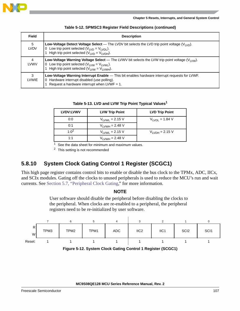
Chapter 5 Resets, Interrupts, and General System Control
5.8.10 System Clock Gating Control 1 Register (SCGC1)
This high page register contains control bits to enable or disable the bus clock to the TPMx, ADC, IICx,and SCIx modules. Gating off the clocks to unused peripherals is used to reduce the MCU’s run and waitcurrents. See Section 5.7, “Peripheral Clock Gating,” for more information.
NOTEUser software should disable the peripheral before disabling the clocks tothe peripheral. When clocks are re-enabled to a peripheral, the peripheralregisters need to be re-initialized by user software.
5LVDV
Low-Voltage Detect Voltage Select — The LVDV bit selects the LVD trip point voltage (VLVD).0 Low trip point selected (VLVD = VLVDL).1 High trip point selected (VLVD = VLVDH).
4LVWV
Low-Voltage Warning Voltage Select — The LVWV bit selects the LVW trip point voltage (VLVW).0 Low trip point selected (VLVW = VLVWL).1 High trip point selected (VLVW = VLVWH).
3LVWIE
Low-Voltage Warning Interrupt Enable — This bit enables hardware interrupt requests for LVWF.0 Hardware interrupt disabled (use polling).1 Request a hardware interrupt when LVWF = 1.
Table 5-13. LVD and LVW Trip Point Typical Values1
1 See the data sheet for minimum and maximum values.
LVDV:LVWV LVW Trip Point LVD Trip Point
0:0 VLVWL = 2.15 V VLVDL = 1.84 V
0:1 VLVWH = 2.48 V
1:02
2 This setting is not recommended
VLVWL = 2.15 V VLVDH = 2.15 V
1:1 VLVWH = 2.48 V
7 6 5 4 3 2 1 0
RTPM3 TPM2 TPM1 ADC IIC2 IIC1 SCI2 SCI1
W
Reset: 1 1 1 1 1 1 1 1
Figure 5-12. System Clock Gating Control 1 Register (SCGC1)
Table 5-12. SPMSC3 Register Field Descriptions (continued)
Field Description
MC9S08QE128 MCU Series Reference Manual, Rev. 2
Freescale Semiconductor 107
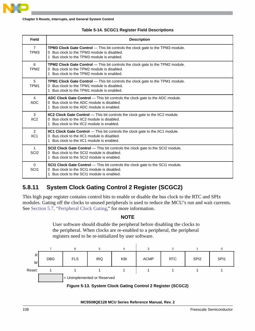
Chapter 5 Resets, Interrupts, and General System Control
5.8.11 System Clock Gating Control 2 Register (SCGC2)
This high page register contains control bits to enable or disable the bus clock to the RTC and SPIxmodules. Gating off the clocks to unused peripherals is used to reduce the MCU’s run and wait currents.See Section 5.7, “Peripheral Clock Gating,” for more information.
NOTEUser software should disable the peripheral before disabling the clocks tothe peripheral. When clocks are re-enabled to a peripheral, the peripheralregisters need to be re-initialized by user software.
Table 5-14. SCGC1 Register Field Descriptions
Field Description
7TPM3
TPM3 Clock Gate Control — This bit controls the clock gate to the TPM3 module.0 Bus clock to the TPM3 module is disabled.1 Bus clock to the TPM3 module is enabled.
6TPM2
TPM2 Clock Gate Control — This bit controls the clock gate to the TPM2 module.0 Bus clock to the TPM2 module is disabled.1 Bus clock to the TPM2 module is enabled.
5TPM1
TPM1 Clock Gate Control — This bit controls the clock gate to the TPM1 module.0 Bus clock to the TPM1 module is disabled.1 Bus clock to the TPM1 module is enabled.
4ADC
ADC Clock Gate Control — This bit controls the clock gate to the ADC module.0 Bus clock to the ADC module is disabled.1 Bus clock to the ADC module is enabled.
3IIC2
IIC2 Clock Gate Control — This bit controls the clock gate to the IIC2 module.0 Bus clock to the IIC2 module is disabled.1 Bus clock to the IIC2 module is enabled.
2IIC1
IIC1 Clock Gate Control — This bit controls the clock gate to the IIC1 module.0 Bus clock to the IIC1 module is disabled.1 Bus clock to the IIC1 module is enabled.
1SCI2
SCI2 Clock Gate Control — This bit controls the clock gate to the SCI2 module.0 Bus clock to the SCI2 module is disabled.1 Bus clock to the SCI2 module is enabled.
0SCI1
SCI1 Clock Gate Control — This bit controls the clock gate to the SCI1 module.0 Bus clock to the SCI1 module is disabled.1 Bus clock to the SCI1 module is enabled.
7 6 5 4 3 2 1 0
RDBG FLS IRQ KBI ACMP RTC SPI2 SPI1
W
Reset: 1 1 1 1 1 1 1 1
= Unimplemented or Reserved
Figure 5-13. System Clock Gating Control 2 Register (SCGC2)
MC9S08QE128 MCU Series Reference Manual, Rev. 2
108 Freescale Semiconductor

Chapter 5 Resets, Interrupts, and General System Control
Table 5-15. SCGC2 Register Field Descriptions
Field Description
7DBG
DBG Clock Gate Control — This bit controls the bus clock gate to the DBG module.0 Bus clock to the DBG module is disabled.1 Bus clock to the DBG module is enabled.
6FLS
Flash Register Clock Gate Control — This bit controls the bus clock gate to the flash registers. This bit doesnot affect normal program execution from with the flash array. Only the clock to the flash control registers isaffected.0 Bus clock to the flash registers is disabled.1 Bus clock to the flash registers is enabled.
5IRQ
IRQ Clock Gate Control — This bit controls the bus clock gate to the IRQ module.0 Bus clock to the IRQ module is disabled.1 Bus clock to the IRQ module is enabled.
4KBI
KBI Clock Gate Control — This bit controls the clock gate to both of the KBI modules.0 Bus clock to the KBI modules is disabled.1 Bus clock to the KBI modules is enabled.
3ACMP
ACMP Clock Gate Control — This bit controls the clock gate to both of the ACMP modules.0 Bus clock to the ACMP modules is disabled.1 Bus clock to the ACMP modules is enabled.
2RTC
RTC Clock Gate Control — This bit controls the bus clock gate to the RTC module. Only ICSIRCLK is gated,OSCOUT and LPOCLK are still available to the RTC.0 ICSIRCLK to the RTC module is disabled.1 ICSIRCLK to the RTC module is enabled.
1SPI2
SPI2 Clock Gate Control — This bit controls the clock gate to the SPI2 module.0 Bus clock to the SPI2 module is disabled.1 Bus clock to the SPI2 module is enabled.
0SPI1
SPI1 Clock Gate Control — This bit controls the clock gate to the SPI1 module.0 Bus clock to the SPI1 module is disabled.1 Bus clock to the SPI1 module is enabled.
MC9S08QE128 MCU Series Reference Manual, Rev. 2
Freescale Semiconductor 109

Chapter 5 Resets, Interrupts, and General System Control
MC9S08QE128 MCU Series Reference Manual, Rev. 2
110 Freescale Semiconductor

Chapter 6Parallel Input/Output ControlThis section explains software controls related to parallel input/output (I/O) and pin control. TheMC9S08QE128 has nine parallel I/O ports which include a total of 70 I/O pins and one output-only pin.See Chapter 2, “Pins and Connections,” for more information about pin assignments and external hardwareconsiderations of these pins.
Many of these pins are shared with on-chip peripherals such as timer systems, communication systems, orkeyboard interrupts as shown in Table 2-1. The peripheral modules have priority over the general-purposeI/O functions so that when a peripheral is enabled, the I/O functions associated with the shared pins maybe disabled.
After reset, the shared peripheral functions are disabled and the pins are configured as inputs(PTxDDn = 0). The pin control functions for each pin are configured as follows: slew rate control disabled(PTxSEn = 0), low drive strength selected (PTxDSn = 0), and internal pull-ups disabled (PTxPEn = 0).
NOTENot all general-purpose I/O pins are available on all packages. To avoidextra current drain from floating input pins, the user’s reset initializationroutine in the application program must either enable on-chip pull-updevices or change the direction of unconnected pins to outputs so the pinsdo not float.
6.1 Port Data and Data DirectionReading and writing of parallel I/Os are performed through the port data registers. The direction, eitherinput or output, is controlled through the port data direction registers. The parallel I/O port function for anindividual pin is illustrated in the block diagram shown in Figure 6-1.
The data direction control bit (PTxDDn) determines whether the output buffer for the associated pin isenabled, and also controls the source for port data register reads. The input buffer for the associated pin isalways enabled unless the pin is enabled as an analog function or is an output-only pin.
When a shared digital function is enabled for a pin, the output buffer is controlled by the shared function.However, the data direction register bit will continue to control the source for reads of the port data register.
When a shared analog function is enabled for a pin, both the input and output buffers are disabled. A valueof 0 is read for any port data bit where the bit is an input (PTxDDn = 0) and the input buffer is disabled.In general, whenever a pin is shared with both an alternate digital function and an analog function, theanalog function has priority such that if both the digital and analog functions are enabled, the analogfunction controls the pin.
MC9S08QE128 MCU Series Reference Manual, Rev. 2
Freescale Semiconductor 111

Chapter 6 Parallel Input/Output Control
It is a good programming practice to write to the port data register before changing the direction of a portpin to become an output. This ensures that the pin will not be driven momentarily with an old data valuethat happened to be in the port data register.
Figure 6-1. Parallel I/O Block Diagram
6.2 Pull-up, Slew Rate, and Drive StrengthAssociated with the parallel I/O ports is a set of registers located in the high page register space that operateindependently of the parallel I/O registers. These registers are used to control pull-ups, slew rate, and drivestrength for the pins and may be used in conjunction with the peripheral functions on these pins.
6.2.1 Port Internal Pull-Up Enable
An internal pull-up device can be enabled for each port pin by setting the corresponding bit in the pull-upenable register (PTxPEn). The pull-up device is disabled if the pin is configured as an output by the parallelI/O control logic or any shared peripheral function regardless of the state of the corresponding pull-upenable register bit. The pull-up device is also disabled if the pin is controlled by an analog function.
6.2.2 Port Slew Rate Enable
Slew rate control can be enabled for each port pin by setting the corresponding bit in the slew rate controlregister (PTxSEn). When enabled, slew control limits the rate at which an output can transition in order toreduce EMC emissions. Slew rate control has no effect on pins that are configured as inputs.
6.2.3 Port Drive Strength Select
An output pin can be selected to have high output drive strength by setting the corresponding bit in thedrive strength select register (PTxDSn). When high drive is selected, a pin is capable of sourcing and
QD
QD
1
0
Port Read
PTxDDn
PTxDn
Output Enable
Output Data
Input DataSynchronizer
Data
BUSCLK
MC9S08QE128 MCU Series Reference Manual, Rev. 2
112 Freescale Semiconductor

Chapter 6 Parallel Input/Output Control
sinking greater current. Even though every I/O pin can be selected as high drive, the user must ensure thatthe total current source and sink limits for the MCU are not exceeded. Drive strength selection is intendedto affect the DC behavior of I/O pins. However, the AC behavior is also affected. High drive allows a pinto drive a greater load with the same switching speed as a low drive enabled pin into a smaller load.Because of this, the EMC emissions may be affected by enabling pins as high drive.
6.3 Port Data Set, Clear and Toggle Data RegistersThe Port Data Set, Clear and Toggle registers provide an alternate method for setting and clearingindividual port I/O pins within a single port. Only port C and port E have data set, clear and toggle registers.Figure 6-2 should be contrasted with Figure 6-1 to see the effects of adding Set/Clear/Toggle functionalityto the port cell. SET_Enable, CLR_Enable, and Toggle_Enable will be set to 1 when the user writes to theData Set, Clear or Toggle register, respectively. The bit pattern on the peripheral bus port is then used toperform the requested function on the port data register.
Figure 6-2. Parallel I/O Block Diagram Equipped with SET/CLR Functionality: Ports C & E
QD
QD
1
0
Port Read
PTxDDn
PTxDn
Output Enable
Output Data
Input DataSynchronizerData
BUSCLK
DATA
SET_Enable
CLR_Enable
Module_Enable
TOGGLE_Enable
MC9S08QE128 MCU Series Reference Manual, Rev. 2
Freescale Semiconductor 113

Chapter 6 Parallel Input/Output Control
6.3.1 Port Data Set Registers
The Port Data Set registers (PTxSET) are write only registers associated with ports C & E. Writing to theseregisters has the result: PortData = PortData | SetPattern. A subsequent read of the corresponding port dataregister will reflect the changed result (a one clock cycle delay is required to see the proper value).
6.3.2 Port Data Clear Registers
The Port Data Clear registers (PTxCLR) are write only registers associated with ports C & E. Writing tothese registers has the result: PortData = PortData & NOT ClrPattern. A subsequent read of thecorresponding port data register will reflect the changed result (a one clock cycle delay is required to seethe proper value).
6.3.3 Port Data Toggle Register
The Port Data Toggle registers (PTxTOG) are write only registers associated with ports C & E. Writing tothese registers has the result: PortData[i] = NOT PortData[i] for any bit written as a one to PTxTOG. Asubsequent read of the corresponding port data register will reflect the changed result (a one clock cycledelay is required to see the proper value).
6.4 Pin Behavior in Stop ModesPin behavior following execution of a STOP instruction depends on the stop mode that is entered. Anexplanation of pin behavior for the various stop modes follows:
• Stop2 mode is a partial power-down mode, whereby I/O latches are maintained in their state asbefore the STOP instruction was executed. CPU register status and the state of I/O registers shouldbe saved in RAM before the STOP instruction is executed to place the MCU in stop2 mode. Uponrecovery from stop2 mode, before accessing any I/O, the user should examine the state of the PPDFbit in the SPMSC2 register. If the PPDF bit is 0, I/O must be initialized as if a power on reset hadoccurred. If the PPDF bit is 1, I/O register states should be restored from the values saved in RAMbefore the STOP instruction was executed and peripherals may require initialization or restorationto their pre-stop condition. The user must then write a 1 to the PPDACK bit in the SPMSC2register. Access to I/O is now permitted again in the user application program.
• In stop3 mode, all I/O is maintained because internal logic circuity stays powered up. Uponrecovery, normal I/O function is available to the user.
6.5 Parallel I/O and Pin Control RegistersThis section provides information about the registers associated with the parallel I/O ports. The data anddata direction registers are located in page zero of the memory map. The pull up, slew rate, drive strength,and interrupt control registers are located in the high page section of the memory map.
Refer to tables in Chapter 4, “Memory,” for the absolute address assignments for all parallel I/O and theirpin control registers. This section refers to registers and control bits only by their names. A FreescaleSemiconductor-provided equate or header file normally is used to translate these names into theappropriate absolute addresses.
MC9S08QE128 MCU Series Reference Manual, Rev. 2
114 Freescale Semiconductor

Chapter 6 Parallel Input/Output Control
6.5.1 Port A Registers
Port A is controlled by the registers listed below.
The pins PTA4 and PTA5 are unique. PTA4 is an output only, so the control bits for the input functionswill not have any effect on this pin. PTA5 is an input only, so the control bits for the output functions willnot have any effect on this pin.
6.5.1.1 Port A Data Register (PTAD)
6.5.1.2 Port A Data Direction Register (PTADD)
7 6 5 4 3 2 1 0
RPTAD7 PTAD6
PTAD5PTAD41
1 Reads of bit PTAD4 always return the contents of PTAD4, regardless of the value stored in bit PTADD4.
PTAD3 PTAD2 PTAD1 PTAD0W
Reset: 0 0 0 0 0 0 0 0
Figure 6-3. Port A Data Register (PTAD)
Table 6-1. PTAD Register Field Descriptions
Field Description
7:0PTAD[7:0]
Port A Data Register Bits — For port A pins that are inputs, reads return the logic level on the pin. For port Apins that are configured as outputs, reads return the last value written to this register.Writes are latched into all bits of this register. For port A pins that are configured as outputs, the logic level isdriven out the corresponding MCU pin.Reset forces PTAD to all 0s, but these 0s are not driven out the corresponding pins because reset also configuresall port pins as high-impedance inputs with pull-ups/pull-downs disabled.
7 6 5 4 3 2 1 0
RPTADD7 PTADD6 PTADD51
1 PTADD5 has no effect on the input-only PTA5 pin.
PTADD42
2 PTADD4 has no effect on the output-only PTA4 pin.
PTADD3 PTADD2 PTADD1 PTADD0W
Reset: 0 0 0 0 0 0 0 0
Figure 6-4. Port A Data Direction Register (PTADD)
Table 6-2. PTADD Register Field Descriptions
Field Description
7:0PTADD[7:0]
Data Direction for Port A Bits — These read/write bits control the direction of port A pins and what is read forPTAD reads.0 Input (output driver disabled) and reads return the pin value.1 Output driver enabled for port A bit n and PTAD reads return the contents of PTADn.
MC9S08QE128 MCU Series Reference Manual, Rev. 2
Freescale Semiconductor 115

Chapter 6 Parallel Input/Output Control
6.5.1.3 Port A Pull Enable Register (PTAPE)
The port A enable register (PTAPE) enables pull-ups on the corresponding PTA pin. In some cases, apull-down device will be enabled if pull-downs are supported by an alternative pin function, such as KBI.
6.5.1.4 Port A Slew Rate Enable Register (PTASE)
7 6 5 4 3 2 1 0
RPTAPE7 PTAPE6 PTAPE5 PTAPE41
1 PTAPE4 has no effect on the output-only PTA4 pin.
PTAPE3 PTAPE2 PTAPE1 PTAPE0W
Reset: 0 0 0 0 0 0 0 0
Figure 6-5. Internal Pull Enable for Port A Register (PTAPE)
Table 6-3. PTAPE Register Field Descriptions
Field Description
7:0PTAPE[7:0]
Internal Pull Enable for Port A Bits — Each of these control bits determines if the internal pull-up or pull-downdevice is enabled for the associated PTA pin. For port A pins that are configured as outputs, these bits have noeffect and the internal pull devices are disabled.0 Internal pull-up/pull-down device disabled for port A bit n.1 Internal pull-up/pull-down device enabled for port A bit n.
7 6 5 4 3 2 1 0
RPTASE7 PTASE6 PTASE51
1 PTASE5 will have no effect on the input-only PTA5 pin.
PTASE4 PTASE3 PTASE2 PTASE1 PTASE0W
Reset: 0 0 0 0 0 0 0 0
Figure 6-6. Slew Rate Enable for Port A Register (PTASE)
Table 6-4. PTASE Register Field Descriptions
Field Description
7:0PTASE[7:0]
Output Slew Rate Enable for Port A Bits — Each of these control bits determines if the output slew rate controlis enabled for the associated PTA pin. For port A pins that are configured as inputs, these bits have no effect.0 Output slew rate control disabled for port A bit n.1 Output slew rate control enabled for port A bit n.
MC9S08QE128 MCU Series Reference Manual, Rev. 2
116 Freescale Semiconductor

Chapter 6 Parallel Input/Output Control
6.5.1.5 Port A Drive Strength Selection Register (PTADS)
6.5.2 Port B Registers
Port B is controlled by the registers listed below.
7 6 5 4 3 2 1 0
RPTADS7 PTADS6 PTADS51
1 PTADS5 will have no effect on the input-only PTA5 pin
PTADS4 PTADS3 PTADS2 PTADS1 PTADS0W
Reset: 0 0 0 0 0 0 0 0
Figure 6-7. Drive Strength Selection for Port A Register (PTADS)
Table 6-5. PTADS Register Field Descriptions
Field Description
7:0PTADS[7:0]
Output Drive Strength Selection for Port A Bits — Each of these control bits selects between low and highoutput drive for the associated PTA pin. For port A pins that are configured as inputs, these bits have no effect.0 Low output drive strength selected for port A bit n.1 High output drive strength selected for port A bit n.
MC9S08QE128 MCU Series Reference Manual, Rev. 2
Freescale Semiconductor 117
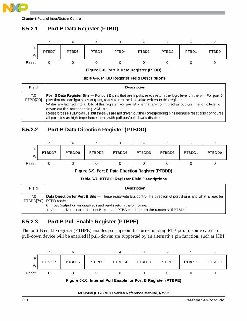
Chapter 6 Parallel Input/Output Control
6.5.2.1 Port B Data Register (PTBD)
6.5.2.2 Port B Data Direction Register (PTBDD)
6.5.2.3 Port B Pull Enable Register (PTBPE)
The port B enable register (PTBPE) enables pull-ups on the corresponding PTB pin. In some cases, apull-down device will be enabled if pull-downs are supported by an alternative pin function, such as KBI.
7 6 5 4 3 2 1 0
RPTBD7 PTBD6 PTBD5 PTBD4 PTBD3 PTBD2 PTBD1 PTBD0
W
Reset: 0 0 0 0 0 0 0 0
Figure 6-8. Port B Data Register (PTBD)
Table 6-6. PTBD Register Field Descriptions
Field Description
7:0PTBD[7:0]
Port B Data Register Bits — For port B pins that are inputs, reads return the logic level on the pin. For port Bpins that are configured as outputs, reads return the last value written to this register.Writes are latched into all bits of this register. For port B pins that are configured as outputs, the logic level isdriven out the corresponding MCU pin.Reset forces PTBD to all 0s, but these 0s are not driven out the corresponding pins because reset also configuresall port pins as high-impedance inputs with pull-ups/pull-downs disabled.
7 6 5 4 3 2 1 0
RPTBDD7 PTBDD6 PTBDD5 PTBDD4 PTBDD3 PTBDD2 PTBDD1 PTBDD0
W
Reset: 0 0 0 0 0 0 0 0
Figure 6-9. Port B Data Direction Register (PTBDD)
Table 6-7. PTBDD Register Field Descriptions
Field Description
7:0PTBDD[7:0]
Data Direction for Port B Bits — These read/write bits control the direction of port B pins and what is read forPTBD reads.0 Input (output driver disabled) and reads return the pin value.1 Output driver enabled for port B bit n and PTBD reads return the contents of PTBDn.
7 6 5 4 3 2 1 0
RPTBPE7 PTBPE6 PTBPE5 PTBPE4 PTBPE3 PTBPE2 PTBPE1 PTBPE0
W
Reset: 0 0 0 0 0 0 0 0
Figure 6-10. Internal Pull Enable for Port B Register (PTBPE)
MC9S08QE128 MCU Series Reference Manual, Rev. 2
118 Freescale Semiconductor

Chapter 6 Parallel Input/Output Control
6.5.2.4 Port B Slew Rate Enable Register (PTBSE)
6.5.2.5 Port B Drive Strength Selection Register (PTBDS)
6.5.3 Port C Registers
Port C is controlled by the registers listed below.
Table 6-8. PTBPE Register Field Descriptions
Field Description
7:0PTBPE[7:0]
Internal Pull Enable for Port B Bits — Each of these control bits determines if the internal pull-up or pull-downdevice is enabled for the associated PTB pin. For port B pins that are configured as outputs, these bits have noeffect and the internal pull devices are disabled.0 Internal pull-up/pull-down device disabled for port B bit n.1 Internal pull-up/pull-down device enabled for port B bit n.
7 6 5 4 3 2 1 0
RPTBSE7 PTBSE6 PTBSE5 PTBSE4 PTBSE3 PTBSE2 PTBSE1 PTBSE0
W
Reset: 0 0 0 0 0 0 0 0
Figure 6-11. Slew Rate Enable for Port B Register (PTBSE)
Table 6-9. PTBSE Register Field Descriptions
Field Description
7:0PTBSE[7:0]
Output Slew Rate Enable for Port B Bits — Each of these control bits determines if the output slew rate controlis enabled for the associated PTB pin. For port B pins that are configured as inputs, these bits have no effect.0 Output slew rate control disabled for port B bit n.1 Output slew rate control enabled for port B bit n.
7 6 5 4 3 2 1 0
RPTBDS7 PTBDS6 PTBDS5 PTBDS4 PTBDS3 PTBDS2 PTBDS1 PTBDS0
W
Reset: 0 0 0 0 0 0 0 0
Figure 6-12. Drive Strength Selection for Port B Register (PTBDS)
Table 6-10. PTBDS Register Field Descriptions
Field Description
7:0PTBDS[7:0]
Output Drive Strength Selection for Port B Bits — Each of these control bits selects between low and highoutput drive for the associated PTB pin. For port B pins that are configured as inputs, these bits have no effect.0 Low output drive strength selected for port B bit n.1 High output drive strength selected for port B bit n.
MC9S08QE128 MCU Series Reference Manual, Rev. 2
Freescale Semiconductor 119
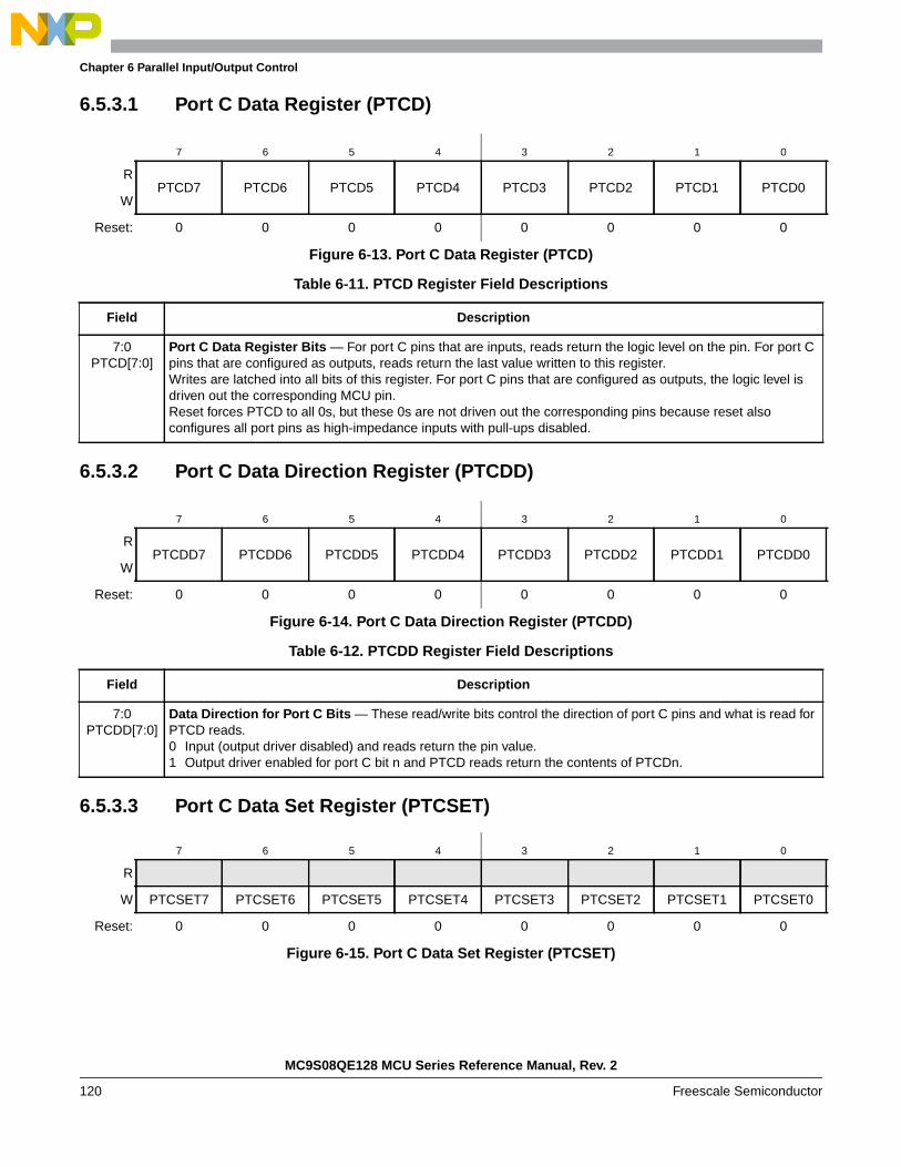
Chapter 6 Parallel Input/Output Control
6.5.3.1 Port C Data Register (PTCD)
6.5.3.2 Port C Data Direction Register (PTCDD)
6.5.3.3 Port C Data Set Register (PTCSET)
7 6 5 4 3 2 1 0
RPTCD7 PTCD6 PTCD5 PTCD4 PTCD3 PTCD2 PTCD1 PTCD0
W
Reset: 0 0 0 0 0 0 0 0
Figure 6-13. Port C Data Register (PTCD)
Table 6-11. PTCD Register Field Descriptions
Field Description
7:0PTCD[7:0]
Port C Data Register Bits — For port C pins that are inputs, reads return the logic level on the pin. For port Cpins that are configured as outputs, reads return the last value written to this register.Writes are latched into all bits of this register. For port C pins that are configured as outputs, the logic level isdriven out the corresponding MCU pin.Reset forces PTCD to all 0s, but these 0s are not driven out the corresponding pins because reset alsoconfigures all port pins as high-impedance inputs with pull-ups disabled.
7 6 5 4 3 2 1 0
RPTCDD7 PTCDD6 PTCDD5 PTCDD4 PTCDD3 PTCDD2 PTCDD1 PTCDD0
W
Reset: 0 0 0 0 0 0 0 0
Figure 6-14. Port C Data Direction Register (PTCDD)
Table 6-12. PTCDD Register Field Descriptions
Field Description
7:0PTCDD[7:0]
Data Direction for Port C Bits — These read/write bits control the direction of port C pins and what is read forPTCD reads.0 Input (output driver disabled) and reads return the pin value.1 Output driver enabled for port C bit n and PTCD reads return the contents of PTCDn.
7 6 5 4 3 2 1 0
R
W PTCSET7 PTCSET6 PTCSET5 PTCSET4 PTCSET3 PTCSET2 PTCSET1 PTCSET0
Reset: 0 0 0 0 0 0 0 0
Figure 6-15. Port C Data Set Register (PTCSET)
MC9S08QE128 MCU Series Reference Manual, Rev. 2
120 Freescale Semiconductor
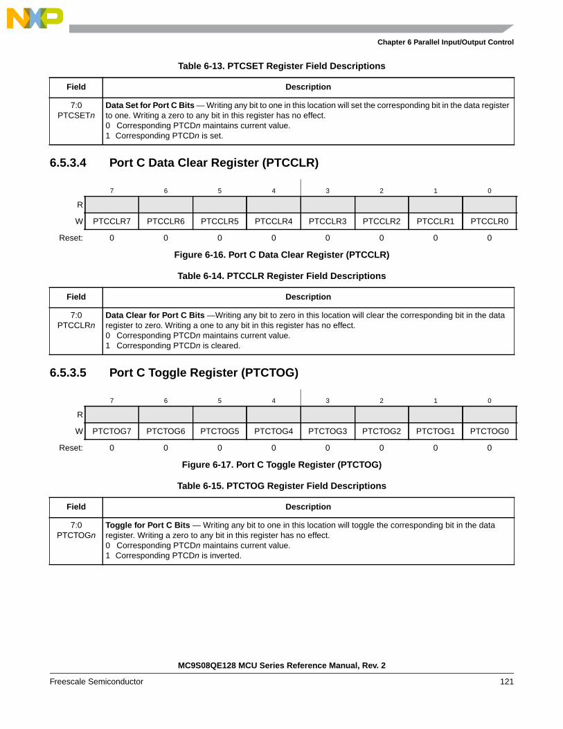
Chapter 6 Parallel Input/Output Control
6.5.3.4 Port C Data Clear Register (PTCCLR)
6.5.3.5 Port C Toggle Register (PTCTOG)
Table 6-13. PTCSET Register Field Descriptions
Field Description
7:0PTCSETn
Data Set for Port C Bits — Writing any bit to one in this location will set the corresponding bit in the data registerto one. Writing a zero to any bit in this register has no effect.0 Corresponding PTCDn maintains current value.1 Corresponding PTCDn is set.
7 6 5 4 3 2 1 0
R
W PTCCLR7 PTCCLR6 PTCCLR5 PTCCLR4 PTCCLR3 PTCCLR2 PTCCLR1 PTCCLR0
Reset: 0 0 0 0 0 0 0 0
Figure 6-16. Port C Data Clear Register (PTCCLR)
Table 6-14. PTCCLR Register Field Descriptions
Field Description
7:0PTCCLRn
Data Clear for Port C Bits —Writing any bit to zero in this location will clear the corresponding bit in the dataregister to zero. Writing a one to any bit in this register has no effect.0 Corresponding PTCDn maintains current value.1 Corresponding PTCDn is cleared.
7 6 5 4 3 2 1 0
R
W PTCTOG7 PTCTOG6 PTCTOG5 PTCTOG4 PTCTOG3 PTCTOG2 PTCTOG1 PTCTOG0
Reset: 0 0 0 0 0 0 0 0
Figure 6-17. Port C Toggle Register (PTCTOG)
Table 6-15. PTCTOG Register Field Descriptions
Field Description
7:0PTCTOGn
Toggle for Port C Bits — Writing any bit to one in this location will toggle the corresponding bit in the dataregister. Writing a zero to any bit in this register has no effect.0 Corresponding PTCDn maintains current value.1 Corresponding PTCDn is inverted.
MC9S08QE128 MCU Series Reference Manual, Rev. 2
Freescale Semiconductor 121
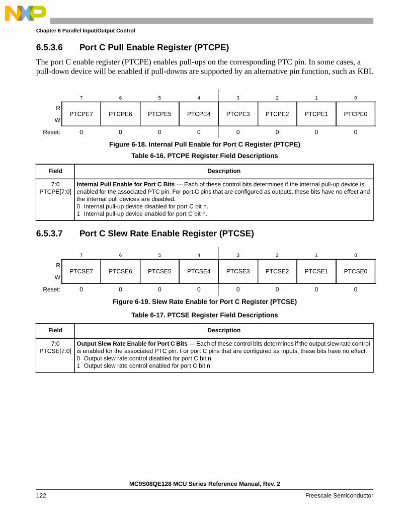
Chapter 6 Parallel Input/Output Control
6.5.3.6 Port C Pull Enable Register (PTCPE)
The port C enable register (PTCPE) enables pull-ups on the corresponding PTC pin. In some cases, apull-down device will be enabled if pull-downs are supported by an alternative pin function, such as KBI.
6.5.3.7 Port C Slew Rate Enable Register (PTCSE)
7 6 5 4 3 2 1 0
RPTCPE7 PTCPE6 PTCPE5 PTCPE4 PTCPE3 PTCPE2 PTCPE1 PTCPE0
W
Reset: 0 0 0 0 0 0 0 0
Figure 6-18. Internal Pull Enable for Port C Register (PTCPE)
Table 6-16. PTCPE Register Field Descriptions
Field Description
7:0PTCPE[7:0]
Internal Pull Enable for Port C Bits — Each of these control bits determines if the internal pull-up device isenabled for the associated PTC pin. For port C pins that are configured as outputs, these bits have no effect andthe internal pull devices are disabled.0 Internal pull-up device disabled for port C bit n.1 Internal pull-up device enabled for port C bit n.
7 6 5 4 3 2 1 0
RPTCSE7 PTCSE6 PTCSE5 PTCSE4 PTCSE3 PTCSE2 PTCSE1 PTCSE0
W
Reset: 0 0 0 0 0 0 0 0
Figure 6-19. Slew Rate Enable for Port C Register (PTCSE)
Table 6-17. PTCSE Register Field Descriptions
Field Description
7:0PTCSE[7:0]
Output Slew Rate Enable for Port C Bits — Each of these control bits determines if the output slew rate controlis enabled for the associated PTC pin. For port C pins that are configured as inputs, these bits have no effect.0 Output slew rate control disabled for port C bit n.1 Output slew rate control enabled for port C bit n.
MC9S08QE128 MCU Series Reference Manual, Rev. 2
122 Freescale Semiconductor

Chapter 6 Parallel Input/Output Control
6.5.3.8 Port C Drive Strength Selection Register (PTCDS)
6.5.4 Port D Registers
Port D is controlled by the registers listed below.
7 6 5 4 3 2 1 0
RPTCDS7 PTCDS6 PTCDS5 PTCDS4 PTCDS3 PTCDS2 PTCDS1 PTCDS0
W
Reset: 0 0 0 0 0 0 0 0
Figure 6-20. Drive Strength Selection for Port C Register (PTCDS)
Table 6-18. PTCDS Register Field Descriptions
Field Description
7:0PTCDS[7:0]
Output Drive Strength Selection for Port C Bits — Each of these control bits selects between low and highoutput drive for the associated PTC pin. For port C pins that are configured as inputs, these bits have no effect.0 Low output drive strength selected for port C bit n.1 High output drive strength selected for port C bit n.
MC9S08QE128 MCU Series Reference Manual, Rev. 2
Freescale Semiconductor 123

Chapter 6 Parallel Input/Output Control
6.5.4.1 Port D Data Register (PTDD)
6.5.4.2 Port D Data Direction Register (PTDDD)
6.5.4.3 Port D Pull Enable Register (PTDPE)
The port D enable register (PTDPE) enables pull-ups on the corresponding PTD pin. In some cases, apull-down device will be enabled if pull-downs are supported by an alternative pin function, such as KBI.
7 6 5 4 3 2 1 0
RPTDD7 PTDD6 PTDD5 PTDD4 PTDD3 PTDD2 PTDD1 PTDD0
W
Reset: 0 0 0 0 0 0 0 0
Figure 6-21. Port D Data Register (PTDD)
Table 6-19. PTDD Register Field Descriptions
Field Description
7:0PTDD[7:0]
Port D Data Register Bits — For port D pins that are inputs, reads return the logic level on the pin. For port Dpins that are configured as outputs, reads return the last value written to this register.Writes are latched into all bits of this register. For port D pins that are configured as outputs, the logic level isdriven out the corresponding MCU pin.Reset forces PTDD to all 0s, but these 0s are not driven out the corresponding pins because reset alsoconfigures all port pins as high-impedance inputs with pull-ups/pull-downs disabled.
7 6 5 4 3 2 1 0
RPTDDD7 PTDDD6 PTDDD5 PTDDD4 PTDDD3 PTDDD2 PTDDD1 PTDDD0
W
Reset: 0 0 0 0 0 0 0 0
Figure 6-22. Port D Data Direction Register (PTDDD)
Table 6-20. PTDDD Register Field Descriptions
Field Description
7:0PTDDD[7:0]
Data Direction for Port D Bits — These read/write bits control the direction of port D pins and what is read forPTDD reads.0 Input (output driver disabled) and reads return the pin value.1 Output driver enabled for port D bit n and PTDD reads return the contents of PTDDn.
7 6 5 4 3 2 1 0
RPTDPE7 PTDPE6 PTDPE5 PTDPE4 PTDPE3 PTDPE2 PTDPE1 PTDPE0
W
Reset: 0 0 0 0 0 0 0 0
Figure 6-23. Internal Pull Enable for Port D Register (PTDPE)
MC9S08QE128 MCU Series Reference Manual, Rev. 2
124 Freescale Semiconductor
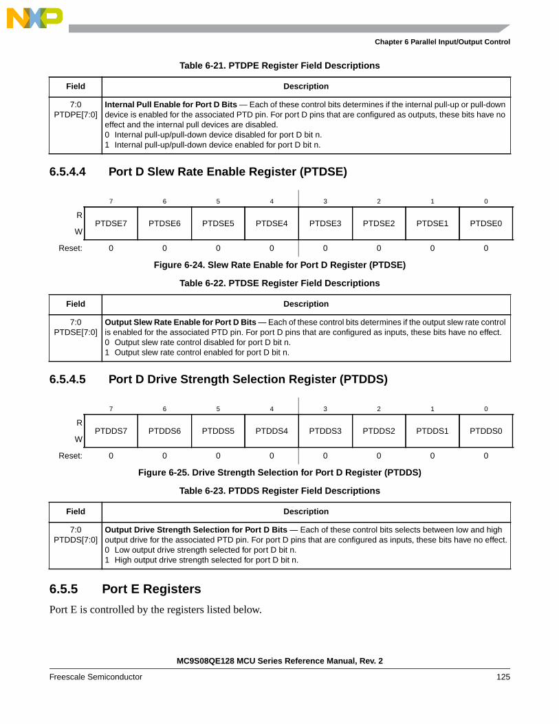
Chapter 6 Parallel Input/Output Control
6.5.4.4 Port D Slew Rate Enable Register (PTDSE)
6.5.4.5 Port D Drive Strength Selection Register (PTDDS)
6.5.5 Port E Registers
Port E is controlled by the registers listed below.
Table 6-21. PTDPE Register Field Descriptions
Field Description
7:0PTDPE[7:0]
Internal Pull Enable for Port D Bits — Each of these control bits determines if the internal pull-up or pull-downdevice is enabled for the associated PTD pin. For port D pins that are configured as outputs, these bits have noeffect and the internal pull devices are disabled.0 Internal pull-up/pull-down device disabled for port D bit n.1 Internal pull-up/pull-down device enabled for port D bit n.
7 6 5 4 3 2 1 0
RPTDSE7 PTDSE6 PTDSE5 PTDSE4 PTDSE3 PTDSE2 PTDSE1 PTDSE0
W
Reset: 0 0 0 0 0 0 0 0
Figure 6-24. Slew Rate Enable for Port D Register (PTDSE)
Table 6-22. PTDSE Register Field Descriptions
Field Description
7:0PTDSE[7:0]
Output Slew Rate Enable for Port D Bits — Each of these control bits determines if the output slew rate controlis enabled for the associated PTD pin. For port D pins that are configured as inputs, these bits have no effect.0 Output slew rate control disabled for port D bit n.1 Output slew rate control enabled for port D bit n.
7 6 5 4 3 2 1 0
RPTDDS7 PTDDS6 PTDDS5 PTDDS4 PTDDS3 PTDDS2 PTDDS1 PTDDS0
W
Reset: 0 0 0 0 0 0 0 0
Figure 6-25. Drive Strength Selection for Port D Register (PTDDS)
Table 6-23. PTDDS Register Field Descriptions
Field Description
7:0PTDDS[7:0]
Output Drive Strength Selection for Port D Bits — Each of these control bits selects between low and highoutput drive for the associated PTD pin. For port D pins that are configured as inputs, these bits have no effect.0 Low output drive strength selected for port D bit n.1 High output drive strength selected for port D bit n.
MC9S08QE128 MCU Series Reference Manual, Rev. 2
Freescale Semiconductor 125

Chapter 6 Parallel Input/Output Control
6.5.5.1 Port E Data Register (PTED)
6.5.5.2 Port E Data Direction Register (PTEDD)
6.5.5.3 Port E Data Set Register (PTESET)
7 6 5 4 3 2 1 0
RPTED7 PTED6 PTED5 PTED4 PTED3 PTED2 PTED1 PTED0
W
Reset: 0 0 0 0 0 0 0 0
Figure 6-26. Port E Data Register (PTED)
Table 6-24. PTED Register Field Descriptions
Field Description
7:0PTED[7:0]
Port E Data Register Bits — For port E pins that are inputs, reads return the logic level on the pin. For port Epins that are configured as outputs, reads return the last value written to this register.Writes are latched into all bits of this register. For port E pins that are configured as outputs, the logic level isdriven out the corresponding MCU pin.Reset forces PTED to all 0s, but these 0s are not driven out the corresponding pins because reset also configuresall port pins as high-impedance inputs with pull-ups disabled.
7 6 5 4 3 2 1 0
RPTEDD7 PTEDD6 PTEDD5 PTEDD4 PTEDD3 PTEDD2 PTEDD1 PTEDD0
W
Reset: 0 0 0 0 0 0 0 0
Figure 6-27. Port E Data Direction Register (PTEDD)
Table 6-25. PTEDD Register Field Descriptions
Field Description
7:0PTEDD[7:0]
Data Direction for Port E Bits — These read/write bits control the direction of port E pins and what is read forPTED reads.0 Input (output driver disabled) and reads return the pin value.1 Output driver enabled for port E bit n and PTED reads return the contents of PTEDn.
7 6 5 4 3 2 1 0
R
W PTESET7 PTESET6 PTESET5 PTESET4 PTESET3 PTESET2 PTESET1 PTESET0
Reset: 0 0 0 0 0 0 0 0
Figure 6-28. Port E Data Set Register (PTESET)
MC9S08QE128 MCU Series Reference Manual, Rev. 2
126 Freescale Semiconductor

Chapter 6 Parallel Input/Output Control
6.5.5.4 Port E Data Clear Register (PTECLR)
6.5.5.5 Port E Toggle Register (PTETOG)
6.5.5.6 Port E Pull Enable Register (PTEPE)
The port E enable register (PTEPE) enables pull-ups on the corresponding PTE pin. In some cases, apull-down device will be enabled if pull-downs are supported by an alternative pin function, such as KBI.
Table 6-26. PTESET Register Field Descriptions
Field Description
7:0PTESETn
Data Set for Port E Bits — Writing any bit to one in this location will set the corresponding bit in the data registerto one. Writing a zero to any bit in this register has no effect.0 Corresponding PTEDn maintains current value.1 Corresponding PTEDn is set.
7 6 5 4 3 2 1 0
R
W PTECLR7 PTECLR6 PTECLR5 PTECLR4 PTECLR3 PTECLR2 PTECLR1 PTECLR0
Reset: 0 0 0 0 0 0 0 0
Figure 6-29. Port E Data Clear Register (PTECLR)
Table 6-27. PTECLR Register Field Descriptions
Field Description
7:0PTECLRn
Data Clear for Port E Bits — Writing any bit to zero in this location will clear the corresponding bit in the dataregister to zero. Writing a one to any bit in this register has no effect.0 Corresponding PTEDn maintains current value.1 Corresponding PTEDn is cleared.
7 6 5 4 3 2 1 0
R
W PTETOG7 PTETOG6 PTETOG5 PTETOG4 PTETOG3 PTETOG2 PTETOG1 PTETOG0
Reset: 0 0 0 0 0 0 0 0
Figure 6-30. Port E Toggle Register (PTETOG)
Table 6-28. PTETOG Register Field Descriptions
Field Description
7:0PTETOGn
Toggle for Port E Bits — Writing any bit to one in this location will toggle the corresponding bit in the dataregister. Writing a zero to any bit in this register has no effect.0 Corresponding PTEDn maintains current value.1 Corresponding PTEDn is inverted.
MC9S08QE128 MCU Series Reference Manual, Rev. 2
Freescale Semiconductor 127
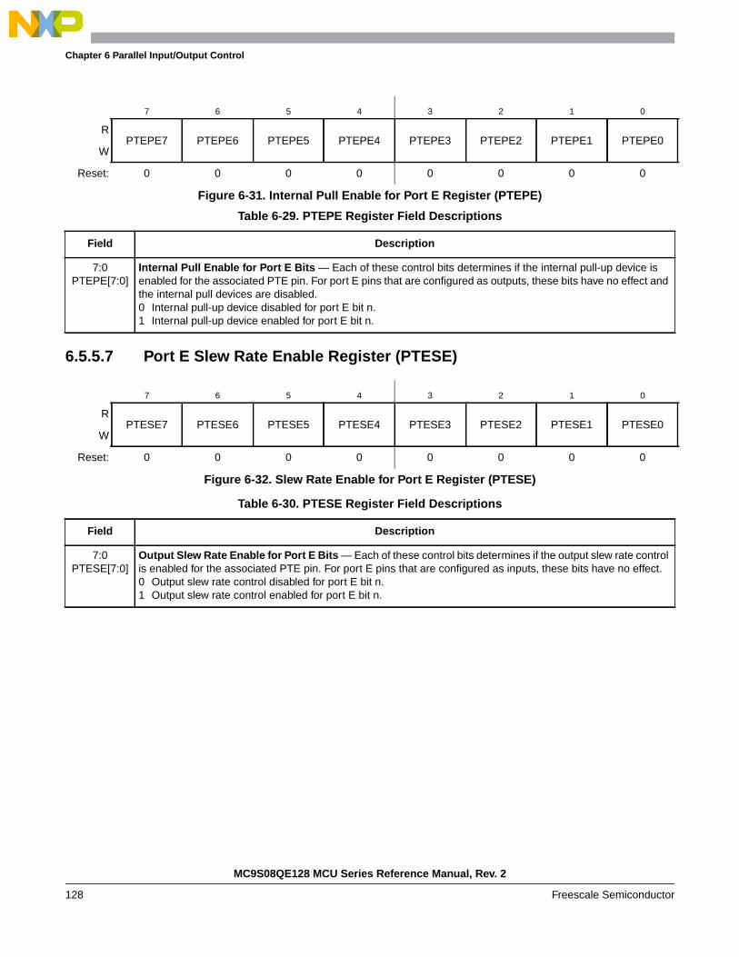
Chapter 6 Parallel Input/Output Control
6.5.5.7 Port E Slew Rate Enable Register (PTESE)
7 6 5 4 3 2 1 0
RPTEPE7 PTEPE6 PTEPE5 PTEPE4 PTEPE3 PTEPE2 PTEPE1 PTEPE0
W
Reset: 0 0 0 0 0 0 0 0
Figure 6-31. Internal Pull Enable for Port E Register (PTEPE)
Table 6-29. PTEPE Register Field Descriptions
Field Description
7:0PTEPE[7:0]
Internal Pull Enable for Port E Bits — Each of these control bits determines if the internal pull-up device isenabled for the associated PTE pin. For port E pins that are configured as outputs, these bits have no effect andthe internal pull devices are disabled.0 Internal pull-up device disabled for port E bit n.1 Internal pull-up device enabled for port E bit n.
7 6 5 4 3 2 1 0
RPTESE7 PTESE6 PTESE5 PTESE4 PTESE3 PTESE2 PTESE1 PTESE0
W
Reset: 0 0 0 0 0 0 0 0
Figure 6-32. Slew Rate Enable for Port E Register (PTESE)
Table 6-30. PTESE Register Field Descriptions
Field Description
7:0PTESE[7:0]
Output Slew Rate Enable for Port E Bits — Each of these control bits determines if the output slew rate controlis enabled for the associated PTE pin. For port E pins that are configured as inputs, these bits have no effect.0 Output slew rate control disabled for port E bit n.1 Output slew rate control enabled for port E bit n.
MC9S08QE128 MCU Series Reference Manual, Rev. 2
128 Freescale Semiconductor

Chapter 6 Parallel Input/Output Control
6.5.5.8 Port E Drive Strength Selection Register (PTEDS)
6.5.6 Port F Registers
Port F is controlled by the registers listed below.
7 6 5 4 3 2 1 0
RPTEDS7 PTEDS6 PTEDS5 PTEDS4 PTEDS3 PTEDS2 PTEDS1 PTEDS0
W
Reset: 0 0 0 0 0 0 0 0
Figure 6-33. Drive Strength Selection for Port E Register (PTEDS)
Table 6-31. PTEDS Register Field Descriptions
Field Description
7:0PTEDS[7:0]
Output Drive Strength Selection for Port E Bits — Each of these control bits selects between low and highoutput drive for the associated PTE pin. For port E pins that are configured as inputs, these bits have no effect.0 Low output drive strength selected for port E bit n.1 High output drive strength selected for port E bit n.
MC9S08QE128 MCU Series Reference Manual, Rev. 2
Freescale Semiconductor 129
Chapter 6 Parallel Input/Output Control
6.5.6.1 Port F Data Register (PTFD)
6.5.6.2 Port F Data Direction Register (PTFDD)
6.5.6.3 Port F Pull Enable Register (PTFPE)
The port F enable register (PTFPE) enables pull-ups on the corresponding PTF pin. In some cases, apull-down device will be enabled if pull-downs are supported by an alternative pin function, such as KBI.
7 6 5 4 3 2 1 0
RPTFD7 PTFD6 PTFD5 PTFD4 PTFD3 PTFD2 PTFD1 PTFD0
W
Reset: 0 0 0 0 0 0 0 0
Figure 6-34. Port F Data Register (PTFD)
Table 6-32. PTFD Register Field Descriptions
Field Description
7:0PTFD[7:0]
Port F Data Register Bits — For port F pins that are inputs, reads return the logic level on the pin. For port Fpins that are configured as outputs, reads return the last value written to this register.Writes are latched into all bits of this register. For port F pins that are configured as outputs, the logic level isdriven out the corresponding MCU pin.Reset forces PTFD to all 0s, but these 0s are not driven out the corresponding pins because reset also configuresall port pins as high-impedance inputs with pull-ups disabled.
7 6 5 4 3 2 1 0
RPTFDD7 PTFDD6 PTFDD5 PTFDD4 PTFDD3 PTFDD2 PTFDD1 PTFDD0
W
Reset: 0 0 0 0 0 0 0 0
Figure 6-35. Port F Data Direction Register (PTFDD)
Table 6-33. PTFDD Register Field Descriptions
Field Description
7:0PTFDD[7:0]
Data Direction for Port F Bits — These read/write bits control the direction of port F pins and what is read forPTFD reads.0 Input (output driver disabled) and reads return the pin value.1 Output driver enabled for port F bit n and PTFD reads return the contents of PTFDn.
7 6 5 4 3 2 1 0
RPTFPE7 PTFPE6 PTFPE5 PTFPE4 PTFPE3 PTFPE2 PTFPE1 PTFPE0
W
Reset: 0 0 0 0 0 0 0 0
Figure 6-36. Internal Pull Enable for Port F Register (PTFPE)
MC9S08QE128 MCU Series Reference Manual, Rev. 2
130 Freescale Semiconductor

Chapter 6 Parallel Input/Output Control
6.5.6.4 Port F Slew Rate Enable Register (PTFSE)
6.5.6.5 Port F Drive Strength Selection Register (PTFDS)
6.5.7 Port G Registers
Port G is controlled by the registers listed below.
Table 6-34. PTFPE Register Field Descriptions
Field Description
7:0PTFPE[7:0]
Internal Pull Enable for Port F Bits — Each of these control bits determines if the internal pull-up device isenabled for the associated PTF pin. For port F pins that are configured as outputs, these bits have no effect andthe internal pull devices are disabled.0 Internal pull-up device disabled for port F bit n.1 Internal pull-up device enabled for port F bit n.
7 6 5 4 3 2 1 0
RPTFSE7 PTFSE6 PTFSE5 PTFSE4 PTFSE3 PTFSE2 PTFSE1 PTFSE0
W
Reset: 0 0 0 0 0 0 0 0
Figure 6-37. Slew Rate Enable for Port F Register (PTFSE)
Table 6-35. PTFSE Register Field Descriptions
Field Description
7:0PTFSE[7:0]
Output Slew Rate Enable for Port F Bits — Each of these control bits determines if the output slew rate controlis enabled for the associated PTF pin. For port F pins that are configured as inputs, these bits have no effect.0 Output slew rate control disabled for port F bit n.1 Output slew rate control enabled for port F bit n.
7 6 5 4 3 2 1 0
RPTFDS7 PTFDS6 PTFDS5 PTFDS4 PTFDS3 PTFDS2 PTFDS1 PTFDS0
W
Reset: 0 0 0 0 0 0 0 0
Figure 6-38. Drive Strength Selection for Port F Register (PTFDS)
Table 6-36. PTFDS Register Field Descriptions
Field Description
7:0PTFDS[7:0]
Output Drive Strength Selection for Port F Bits — Each of these control bits selects between low and highoutput drive for the associated PTF pin. For port F pins that are configured as inputs, these bits have no effect.0 Low output drive strength selected for port F bit n.1 High output drive strength selected for port F bit n.
MC9S08QE128 MCU Series Reference Manual, Rev. 2
Freescale Semiconductor 131

Chapter 6 Parallel Input/Output Control
6.5.7.1 Port G Data Register (PTGD)
6.5.7.2 Port G Data Direction Register (PTGDD)
6.5.7.3 Port G Pull Enable Register (PTGPE)
The port G enable register (PTGPE) enables pull-ups on the corresponding PTG pin. In some cases, apull-down device will be enabled if pull-downs are supported by an alternative pin function, such as KBI.
7 6 5 4 3 2 1 0
RPTGD7 PTGD6 PTGD5 PTGD4 PTGD3 PTGD2 PTGD1 PTGD0
W
Reset: 0 0 0 0 0 0 0 0
Figure 6-39. Port G Data Register (PTGD)
Table 6-37. PTGD Register Field Descriptions
Field Description
7:0PTGD[7:0]
Port G Data Register Bits — For port G pins that are inputs, reads return the logic level on the pin. For port Gpins that are configured as outputs, reads return the last value written to this register.Writes are latched into all bits of this register. For port G pins that are configured as outputs, the logic level isdriven out the corresponding MCU pin.Reset forces PTGD to all 0s, but these 0s are not driven out the corresponding pins because reset alsoconfigures all port pins as high-impedance inputs with pull-ups disabled.
7 6 5 4 3 2 1 0
RPTGDD7 PTGDD6 PTGDD5 PTGDD4 PTGDD3 PTGDD2 PTGDD1 PTGDD0
W
Reset: 0 0 0 0 0 0 0 0
Figure 6-40. Port G Data Direction Register (PTGDD)
Table 6-38. PTGDD Register Field Descriptions
Field Description
7:0PTGDD[7:0]
Data Direction for Port G Bits — These read/write bits control the direction of port G pins and what is read forPTGD reads.0 Input (output driver disabled) and reads return the pin value.1 Output driver enabled for port G bit n and PTGD reads return the contents of PTGDn.
7 6 5 4 3 2 1 0
RPTGPE7 PTGPE6 PTGPE5 PTGPE4 PTGPE3 PTGPE2 PTGPE1 PTGPE0
W
Reset: 0 0 0 0 0 0 0 0
Figure 6-41. Internal Pull Enable for Port G Register (PTGPE)
MC9S08QE128 MCU Series Reference Manual, Rev. 2
132 Freescale Semiconductor

Chapter 6 Parallel Input/Output Control
6.5.7.4 Port G Slew Rate Enable Register (PTGSE)
6.5.7.5 Port G Drive Strength Selection Register (PTGDS)
6.5.8 Port H Registers
Port H is controlled by the registers listed below.
Table 6-39. PTGPE Register Field Descriptions
Field Description
7:0PTGPE[7:0]
Internal Pull Enable for Port G Bits — Each of these control bits determines if the internal pull-up device isenabled for the associated PTG pin. For port G pins that are configured as outputs, these bits have no effect andthe internal pull devices are disabled.0 Internal pull-up device disabled for port G bit n.1 Internal pull-up device enabled for port G bit n.
7 6 5 4 3 2 1 0
RPTGSE7 PTGSE6 PTGSE5 PTGSE4 PTGSE3 PTGSE2 PTGSE1 PTGSE0
W
Reset: 0 0 0 0 0 0 0 0
Figure 6-42. Slew Rate Enable for Port G Register (PTGSE)
Table 6-40. PTGSE Register Field Descriptions
Field Description
7:0PTGSE[7:0]
Output Slew Rate Enable for Port G Bits — Each of these control bits determines if the output slew rate controlis enabled for the associated PTG pin. For port G pins that are configured as inputs, these bits have no effect.0 Output slew rate control disabled for port G bit n.1 Output slew rate control enabled for port G bit n.
7 6 5 4 3 2 1 0
RPTGDS7 PTGDS6 PTGDS5 PTGDS4 PTGDS3 PTGDS2 PTGDS1 PTGDS0
W
Reset: 0 0 0 0 0 0 0 0
Figure 6-43. Drive Strength Selection for Port G Register (PTGDS)
Table 6-41. PTGDS Register Field Descriptions
Field Description
7:0PTGDS[7:0]
Output Drive Strength Selection for Port G Bits — Each of these control bits selects between low and highoutput drive for the associated PTG pin. For port G pins that are configured as inputs, these bits have no effect.0 Low output drive strength selected for port G bit n.1 High output drive strength selected for port G bit n.
MC9S08QE128 MCU Series Reference Manual, Rev. 2
Freescale Semiconductor 133

Chapter 6 Parallel Input/Output Control
6.5.8.1 Port H Data Register (PTHD)
6.5.8.2 Port H Data Direction Register (PTHDD)
6.5.8.3 Port H Pull Enable Register (PTHPE)
The port H enable register (PTHPE) enables pull-ups on the corresponding PTH pin. In some cases, apull-down device will be enabled if pull-downs are supported by an alternative pin function, such as KBI.
7 6 5 4 3 2 1 0
RPTHD7 PTHD6 PTHD5 PTHD4 PTHD3 PTHD2 PTHD1 PTHD0
W
Reset: 0 0 0 0 0 0 0 0
Figure 6-44. Port H Data Register (PTHD)
Table 6-42. PTHD Register Field Descriptions
Field Description
7:0PTHD[7:0]
Port H Data Register Bits — For port H pins that are inputs, reads return the logic level on the pin. For port Hpins that are configured as outputs, reads return the last value written to this register.Writes are latched into all bits of this register. For port H pins that are configured as outputs, the logic level isdriven out the corresponding MCU pin.Reset forces PTHD to all 0s, but these 0s are not driven out the corresponding pins because reset alsoconfigures all port pins as high-impedance inputs with pull-ups disabled.
7 6 5 4 3 2 1 0
RPTHDD7 PTHDD6 PTHDD5 PTHDD4 PTHDD3 PTHDD2 PTHDD1 PTHDD0
W
Reset: 0 0 0 0 0 0 0 0
Figure 6-45. Port H Data Direction Register (PTHDD)
Table 6-43. PTHDD Register Field Descriptions
Field Description
7:0PTHDD[7:0]
Data Direction for Port H Bits — These read/write bits control the direction of port H pins and what is read forPTHD reads.0 Input (output driver disabled) and reads return the pin value.1 Output driver enabled for port H bit n and PTHD reads return the contents of PTHDn.
7 6 5 4 3 2 1 0
RPTHPE7 PTHPE6 PTHPE5 PTHPE4 PTHPE3 PTHPE2 PTHPE1 PTHPE0
W
Reset: 0 0 0 0 0 0 0 0
Figure 6-46. Internal Pull Enable for Port H Register (PTHPE)
MC9S08QE128 MCU Series Reference Manual, Rev. 2
134 Freescale Semiconductor

Chapter 6 Parallel Input/Output Control
6.5.8.4 Port H Slew Rate Enable Register (PTHSE)
6.5.8.5 Port H Drive Strength Selection Register (PTHDS)
6.5.9 Port J Registers
Port J is controlled by the registers listed below.
Table 6-44. PTHPE Register Field Descriptions
Field Description
7:0PTHPE[7:0]
Internal Pull Enable for Port H Bits — Each of these control bits determines if the internal pull-up device isenabled for the associated PTH pin. For port H pins that are configured as outputs, these bits have no effect andthe internal pull devices are disabled.0 Internal pull-up device disabled for port H bit n.1 Internal pull-up device enabled for port H bit n.
7 6 5 4 3 2 1 0
RPTHSE7 PTHSE6 PTHSE5 PTHSE4 PTHSE3 PTHSE2 PTHSE1 PTHSE0
W
Reset: 0 0 0 0 0 0 0 0
Figure 6-47. Slew Rate Enable for Port H Register (PTHSE)
Table 6-45. PTHSE Register Field Descriptions
Field Description
7:0PTHSE[7:0]
Output Slew Rate Enable for Port H Bits — Each of these control bits determines if the output slew rate controlis enabled for the associated PTH pin. For port H pins that are configured as inputs, these bits have no effect.0 Output slew rate control disabled for port H bit n.1 Output slew rate control enabled for port H bit n.
7 6 5 4 3 2 1 0
RPTHDS7 PTHDS6 PTHDS5 PTHDS4 PTHDS3 PTHDS2 PTHDS1 PTHDS0
W
Reset: 0 0 0 0 0 0 0 0
Figure 6-48. Drive Strength Selection for Port H Register (PTHDS)
Table 6-46. PTHDS Register Field Descriptions
Field Description
7:0PTHDS[7:0]
Output Drive Strength Selection for Port H Bits — Each of these control bits selects between low and highoutput drive for the associated PTH pin. For port H pins that are configured as inputs, these bits have no effect.0 Low output drive strength selected for port H bit n.1 High output drive strength selected for port H bit n.
MC9S08QE128 MCU Series Reference Manual, Rev. 2
Freescale Semiconductor 135

Chapter 6 Parallel Input/Output Control
6.5.9.1 Port J Data Register (PTJD)
6.5.9.2 Port J Data Direction Register (PTJDD)
6.5.9.3 Port J Pull Enable Register (PTJPE)
The port J enable register (PTJPE) enables pull-ups on the corresponding PTJ pin. In some cases, apull-down device will be enabled if pull-downs are supported by an alternative pin function, such as KBI.
7 6 5 4 3 2 1 0
RPTJD7 PTJD6 PTJD5 PTJD4 PTJD3 PTJD2 PTJD1 PTJD0
W
Reset: 0 0 0 0 0 0 0 0
Figure 6-49. Port J Data Register (PTJD)
Table 6-47. PTJD Register Field Descriptions
Field Description
7:0PTJD[7:0]
Port J Data Register Bits — For port J pins that are inputs, reads return the logic level on the pin. For port Jpins that are configured as outputs, reads return the last value written to this register.Writes are latched into all bits of this register. For port J pins that are configured as outputs, the logic level isdriven out the corresponding MCU pin.Reset forces PTJD to all 0s, but these 0s are not driven out the corresponding pins because reset also configuresall port pins as high-impedance inputs with pull-ups disabled.
7 6 5 4 3 2 1 0
RPTJDD7 PTJDD6 PTJDD5 PTJDD4 PTJDD3 PTJDD2 PTJDD1 PTJDD0
W
Reset: 0 0 0 0 0 0 0 0
Figure 6-50. Port J Data Direction Register (PTJDD)
Table 6-48. PTJDD Register Field Descriptions
Field Description
7:0PTJDD[7:0]
Data Direction for Port J Bits — These read/write bits control the direction of port J pins and what is read forPTJD reads.0 Input (output driver disabled) and reads return the pin value.1 Output driver enabled for port J bit n and PTJD reads return the contents of PTJDn.
7 6 5 4 3 2 1 0
RPTJPE7 PTJPE6 PTJPE5 PTJPE4 PTJPE3 PTJPE2 PTJPE1 PTJPE0
W
Reset: 0 0 0 0 0 0 0 0
Figure 6-51. Internal Pull Enable for Port J Register (PTJPE)
MC9S08QE128 MCU Series Reference Manual, Rev. 2
136 Freescale Semiconductor

Chapter 6 Parallel Input/Output Control
6.5.9.4 Port J Slew Rate Enable Register (PTJSE)
6.5.9.5 Port J Drive Strength Selection Register (PTJDS)
Table 6-49. PTJPE Register Field Descriptions
Field Description
7:0PTJPE[7:0]
Internal Pull Enable for Port J Bits — Each of these control bits determines if the internal pull-up device isenabled for the associated PTJ pin. For port J pins that are configured as outputs, these bits have no effect andthe internal pull devices are disabled.0 Internal pull-up device disabled for port J bit n.1 Internal pull-up device enabled for port J bit n.
7 6 5 4 3 2 1 0
RPTJSE7 PTJSE6 PTJSE5 PTJSE4 PTJSE3 PTJSE2 PTJSE1 PTJSE0
W
Reset: 0 0 0 0 0 0 0 0
Figure 6-52. Slew Rate Enable for Port J Register (PTJSE)
Table 6-50. PTJSE Register Field Descriptions
Field Description
7:0PTJSE[7:0]
Output Slew Rate Enable for Port J Bits — Each of these control bits determines if the output slew rate controlis enabled for the associated PTJ pin. For port J pins that are configured as inputs, these bits have no effect.0 Output slew rate control disabled for port J bit n.1 Output slew rate control enabled for port J bit n.
7 6 5 4 3 2 1 0
RPTJDS7 PTJDS6 PTJDS5 PTJDS4 PTJDS3 PTJDS2 PTJDS1 PTJDS0
W
Reset: 0 0 0 0 0 0 0 0
Figure 6-53. Drive Strength Selection for Port J Register (PTJDS)
Table 6-51. PTJDS Register Field Descriptions
Field Description
7:0PTJDS[7:0]
Output Drive Strength Selection for Port J Bits — Each of these control bits selects between low and highoutput drive for the associated PTJ pin. For port J pins that are configured as inputs, these bits have no effect.0 Low output drive strength selected for port J bit n.1 High output drive strength selected for port J bit n.
MC9S08QE128 MCU Series Reference Manual, Rev. 2
Freescale Semiconductor 137

Chapter 6 Parallel Input/Output Control
MC9S08QE128 MCU Series Reference Manual, Rev. 2
138 Freescale Semiconductor

Chapter 7Keyboard Interrupt (S08KBIV2)
7.1 IntroductionThe keyboard interrupt (KBI) module provides up to eight independently enabled external interruptsources. MC9S08QE128 Series devices contain two KBI modules, called KBI1 and KBI2. Each KBImodule has up to eight interrupt sources.
7.1.1 KBI Clock Gating
The bus clock to the KBI can be gated on and off using the KBI bit in SCGC2. This bit is set after anyreset, which enables the bus clock to this module. To conserve power, the KBI bit can be cleared to disablethe clock to this module when not in use. See Section 5.7, “Peripheral Clock Gating,” for details.
7.1.2 Features
The KBI features include:
• Up to eight keyboard interrupt pins with individual pin enable bits.
• Each keyboard interrupt pin is programmable as falling edge (or rising edge) only, or both fallingedge and low level (or both rising edge and high level) interrupt sensitivity.
• One software enabled keyboard interrupt.
• Exit from low-power modes.
7.1.3 Modes of Operation
This section defines the KBI operation in wait, stop, and background debug modes.
7.1.3.1 KBI in Wait Mode
The KBI continues to operate in wait mode if enabled before executing the WAIT instruction. Therefore,an enabled KBI pin (KBPEx = 1) can be used to bring the MCU out of wait mode if the KBI interrupt isenabled (KBIE = 1).
7.1.3.2 KBI in Stop Modes
The KBI operates asynchronously in stop3 mode if enabled before executing the STOP instruction.Therefore, an enabled KBI pin (KBPEx = 1) can be used to bring the MCU out of stop3 mode if the KBIinterrupt is enabled (KBIE = 1).
MC9S08QE128 MCU Series Reference Manual, Rev. 2
Freescale Semiconductor 139
Chapter 7 Keyboard Interrupt (S08KBIV2)
During stop2 mode, the KBI is disabled. Upon wake-up from stop2 mode, the KBI module will be in thereset state.
7.1.3.3 KBI in Active Background Mode
When the microcontroller is in active background mode, the KBI will continue to operate normally.
7.1.4 Block Diagram
The block diagram for the keyboard interrupt module is shown Figure 7-1.
Figure 7-1. KBI Block Diagram
7.2 External Signal DescriptionThe KBI input pins can be used to detect either falling edges, or both falling edge and low level interruptrequests. The KBI input pins can also be used to detect either rising edges, or both rising edge and highlevel interrupt requests.
Table 7-1. KBI1 Pin Mapping
Port Pin PTB3 PTB2 PTB1 PTB0 PTA3 PTA2 PTA1 PTA0
KBI1 Pin KBI1P7 KBI1P6 KBI1P5 KBI1P4 KBI1P3 KBI1P2 KBI1P1 KBI1P0
Table 7-2. KBI2 Pin Mapping
Port Pin PTD7 PTD6 PTD5 PTD4 PTD3 PTD2 PTD1 PTD0
KBI2 Pin KBI2P7 KBI2P6 KBI2P5 KBI2P4 KBI2P3 KBI2P2 KBI2P1 KBI2P0
D Q
CK
CLR
VDD
KBMOD
KBIE
KEYBOARDINTERRUPT FF
KBACK
RESET
SYNCHRONIZER
KBF
STOP BYPASSSTOP
BUSCLK
KBIPEn0
1
S
KBEDGn
KBIPE00
1
S
KBEDG0
KBIP0
KBIPn
KBIINTERRUPTREQUEST
MC9S08QE128 MCU Series Reference Manual, Rev. 2
140 Freescale Semiconductor
Chapter 7 Keyboard Interrupt (S08KBIV2)
7.3 Register DefinitionThe KBI includes three registers:
• An 8-bit pin status and control register.
• An 8-bit pin enable register.
• An 8-bit edge select register.
Refer to the direct-page register summary in the Memory chapter for the absolute address assignments forall KBI registers. This section refers to registers and control bits only by their names and relative addressoffsets.
Some MCUs may have more than one KBI, so register names include placeholder characters to identifywhich KBI is being referenced.
7.3.1 KBI Interrupt Status and Control Register (KBIxSC)
7 6 5 4 3 2 1 0
R 0 0 0 0 KBF 0KBIE KBIMOD
W KBACK
Reset: 0 0 0 0 0 0 0 0
Figure 7-2. KBI Interrupt Status and Control Register (KBIxSC)
Table 7-3. KBIxSC Register Field Descriptions
Field Description
3KBF
KBI Interrupt Flag — KBF indicates when a KBI interrupt is detected. Writes have no effect on KBF.0 No KBI interrupt detected.1 KBI interrupt detected.
2KBACK
KBI Interrupt Acknowledge — Writing a 1 to KBACK is part of the flag clearing mechanism. KBACK alwaysreads as 0.
1KBIE
KBI Interrupt Enable — KBIE determines whether a KBI interrupt is requested.0 KBI interrupt request not enabled.1 KBI interrupt request enabled.
0KBIMOD
KBI Detection Mode — KBIMOD (along with the KBIES bits) controls the detection mode of the KBI interruptpins.0 KBI pins detect edges only.1 KBI pins detect both edges and levels.
MC9S08QE128 MCU Series Reference Manual, Rev. 2
Freescale Semiconductor 141

Chapter 7 Keyboard Interrupt (S08KBIV2)
7.3.2 KBI Interrupt Pin Select Register (KBIxPE)
7.3.3 KBI Interrupt Edge Select Register (KBIxES)
7.4 Functional DescriptionWriting to the KBIPEn bits in the keyboard x interrupt pin enable register (KBIxPE) independently enablesor disables each port pin. Each port can be configured as edge sensitive or edge and level sensitive basedon the KBIMOD bit in the keyboard interrupt status and control register (KBIxSC). Edge sensitivity canbe software programmed to be either falling or rising; the level can be either low or high. The polarity ofthe edge or edge and level sensitivity is selected using the KBEDGn bits in the keyboard interrupt edgeselect register (KBIxES).
Synchronous logic is used to detect edges. Prior to detecting an edge, enabled port inputs must be at thedeasserted logic level. A falling edge is detected when an enabled port input signal is seen as a logic 1 (thedeasserted level) during one bus cycle and then a logic 0 (the asserted level) during the next cycle. A rising
7 6 5 4 3 2 1 0
RKBIPE7 KBIPE6 KBIPE5 KBIPE4 KBIPE3 KBIPE2 KBIPE1 KBIPE0
W
Reset: 0 0 0 0 0 0 0 0
Figure 7-3. KBI Interrupt Pin Select Register (KBIxPE)
Table 7-4. KBIxPE Register Field Descriptions
Field Description
7:0KBIPE[7:0]
KBI Interrupt Pin Selects — Each of the KBIPEn bits enable the corresponding KBI interrupt pin.0 Pin not enabled as interrupt.1 Pin enabled as interrupt.
7 6 5 4 3 2 1 0
RKBEDG7 KBEDG6 KBEDG5 KBEDG4 KBEDG3 KBEDG2 KBEDG1 KBEDG0
W
Reset: 0 0 0 0 0 0 0 0
Figure 7-4. KBI Edge Select Register (KBIxES)
Table 7-5. KBIxES Register Field Descriptions
Field Description
7:0KBEDG[7:0]
KBI Edge Selects — Each of the KBEDGn bits serves a dual purpose by selecting the polarity of the activeinterrupt edge as well as selecting a pull-up or pull-down device if enabled.0 A pull-up device is connected to the associated pin and detects falling edge/low level for interrupt generation.1 A pull-down device is connected to the associated pin and detects rising edge/high level for interrupt
generation.
MC9S08QE128 MCU Series Reference Manual, Rev. 2
142 Freescale Semiconductor

Chapter 7 Keyboard Interrupt (S08KBIV2)
edge is detected when the input signal is seen as a logic 0 during one bus cycle and then a logic 1 duringthe next cycle.
7.4.1 Edge Only Sensitivity
A valid edge on an enabled port pin will set KBF in KBIxSC. If KBIE in KBIxSC is set, an interruptrequest will be presented to the CPU. Clearing of KBF is accomplished by writing a 1 to KBACK inKBIxSC.
7.4.2 Edge and Level Sensitivity
A valid edge or level on an enabled port pin will set KBF in KBIxSC. If KBIE in KBIxSC is set, aninterrupt request will be presented to the CPU. Clearing of KBF is accomplished by writing a 1 to KBACKin KBIxSC provided all enabled port inputs are at their deasserted levels. KBF will remain set if anyenabled port pin is asserted while attempting to clear by writing a 1 to KBACK.
7.4.3 Pull-Up/Pull-Down Resistors
The keyboard interrupt pins can be configured to use an internal pull-up/pull-down resistor using theassociated I/O port pull-up enable register. If an internal resistor is enabled, the KBIxES register is used toselect whether the resistor is a pull-up (KBEDGn = 0) or a pull-down (KBEDGn = 1).
7.4.4 Keyboard Interrupt Initialization
When an interrupt pin is first enabled, it is possible to get a false interrupt flag. To prevent a false interruptrequest during pin interrupt initialization, the user should do the following:
1. Mask interrupts by clearing KBIE in KBIxSC.
2. Select the pin polarity by setting the appropriate KBEDGn bits in KBIxES.
3. If using internal pull-up/pull-down device, configure the associated pull enable bits in KBIxPE.
4. Enable the interrupt pins by setting the appropriate KBIPEn bits in KBIxPE.
5. Write to KBACK in KBIxSC to clear any false interrupts.
6. Set KBIE in KBIxSC to enable interrupts.
MC9S08QE128 MCU Series Reference Manual, Rev. 2
Freescale Semiconductor 143

Chapter 7 Keyboard Interrupt (S08KBIV2)
MC9S08QE128 MCU Series Reference Manual, Rev. 2
144 Freescale Semiconductor

Chapter 8Central Processor Unit (S08CPUV4)
8.1 IntroductionThis section provides summary information about the registers, addressing modes, and instruction set ofthe CPU of the HCS08 Family. For a more detailed discussion, refer to the HCS08 Family ReferenceManual, volume 1, Freescale Semiconductor document order number HCS08RMV1/D.
The HCS08 CPU is fully source- and object-code-compatible with the M68HC08 CPU. Severalinstructions and enhanced addressing modes were added to improve C compiler efficiency and to supporta new background debug system which replaces the monitor mode of earlier M68HC08 microcontrollers(MCU).
8.1.1 Features
Features of the HCS08 CPU include:
• Object code fully upward-compatible with M68HC05 and M68HC08 Families
• 64-KB CPU address space with banked memory management unit for greater than 64 KB
• 16-bit stack pointer (any size stack anywhere in 64-KB CPU address space)
• 16-bit index register (H:X) with powerful indexed addressing modes
• 8-bit accumulator (A)
• Many instructions treat X as a second general-purpose 8-bit register
• Seven addressing modes:
— Inherent — Operands in internal registers
— Relative — 8-bit signed offset to branch destination
— Immediate — Operand in next object code byte(s)
— Direct — Operand in memory at 0x0000–0x00FF
— Extended — Operand anywhere in 64-Kbyte address space
— Indexed relative to H:X — Five submodes including auto increment
— Indexed relative to SP — Improves C efficiency dramatically
• Memory-to-memory data move instructions with four address mode combinations
• Overflow, half-carry, negative, zero, and carry condition codes support conditional branching onthe results of signed, unsigned, and binary-coded decimal (BCD) operations
• Efficient bit manipulation instructions
• Fast 8-bit by 8-bit multiply and 16-bit by 8-bit divide instructions
• STOP and WAIT instructions to invoke low-power operating modes
MC9S08QE128 MCU Series Reference Manual, Rev. 2
Freescale Semiconductor 145

Chapter 8 Central Processor Unit (S08CPUV4)
8.2 Programmer’s Model and CPU RegistersFigure 8-1 shows the five CPU registers. CPU registers are not part of the memory map.
Figure 8-1. CPU Registers
8.2.1 Accumulator (A)
The A accumulator is a general-purpose 8-bit register. One operand input to the arithmetic logic unit(ALU) is connected to the accumulator and the ALU results are often stored into the A accumulator afterarithmetic and logical operations. The accumulator can be loaded from memory using various addressingmodes to specify the address where the loaded data comes from, or the contents of A can be stored tomemory using various addressing modes to specify the address where data from A will be stored.
Reset has no effect on the contents of the A accumulator.
8.2.2 Index Register (H:X)
This 16-bit register is actually two separate 8-bit registers (H and X), which often work together as a 16-bitaddress pointer where H holds the upper byte of an address and X holds the lower byte of the address. Allindexed addressing mode instructions use the full 16-bit value in H:X as an index reference pointer;however, for compatibility with the earlier M68HC05 Family, some instructions operate only on thelow-order 8-bit half (X).
Many instructions treat X as a second general-purpose 8-bit register that can be used to hold 8-bit datavalues. X can be cleared, incremented, decremented, complemented, negated, shifted, or rotated. Transferinstructions allow data to be transferred from A or transferred to A where arithmetic and logical operationscan then be performed.
For compatibility with the earlier M68HC05 Family, H is forced to 0x00 during reset. Reset has no effecton the contents of X.
SP
PC
CONDITION CODE REGISTER
CARRYZERONEGATIVEINTERRUPT MASKHALF-CARRY (FROM BIT 3)TWO’S COMPLEMENT OVERFLOW
H X
0
0
0
7
15
15
7 0
ACCUMULATOR A
INDEX REGISTER (LOW)INDEX REGISTER (HIGH)
STACK POINTER
8 7
PROGRAM COUNTER
16-BIT INDEX REGISTER H:X
CCRCV 1 1 H I N Z
MC9S08QE128 MCU Series Reference Manual, Rev. 2
146 Freescale Semiconductor

Chapter 8 Central Processor Unit (S08CPUV4)
8.2.3 Stack Pointer (SP)
This 16-bit address pointer register points at the next available location on the automatic last-in-first-out(LIFO) stack. The stack may be located anywhere in the 64-Kbyte address space that has RAM and canbe any size up to the amount of available RAM. The stack is used to automatically save the return addressfor subroutine calls, the return address and CPU registers during interrupts, and for local variables. TheAIS (add immediate to stack pointer) instruction adds an 8-bit signed immediate value to SP. This is mostoften used to allocate or deallocate space for local variables on the stack.
SP is forced to 0x00FF at reset for compatibility with the earlier M68HC05 Family. HCS08 programsnormally change the value in SP to the address of the last location (highest address) in on-chip RAMduring reset initialization to free up direct page RAM (from the end of the on-chip registers to 0x00FF).
The RSP (reset stack pointer) instruction was included for compatibility with the M68HC05 Family andis seldom used in new HCS08 programs because it only affects the low-order half of the stack pointer.
8.2.4 Program Counter (PC)
The program counter is a 16-bit register that contains the address of the next instruction or operand to befetched.
During normal program execution, the program counter automatically increments to the next sequentialmemory location every time an instruction or operand is fetched. Jump, branch, interrupt, and returnoperations load the program counter with an address other than that of the next sequential location. Thisis called a change-of-flow.
During reset, the program counter is loaded with the reset vector that is located at 0xFFFE and 0xFFFF.The vector stored there is the address of the first instruction that will be executed after exiting the resetstate.
8.2.5 Condition Code Register (CCR)
The 8-bit condition code register contains the interrupt mask (I) and five flags that indicate the results ofthe instruction just executed. Bits 6 and 5 are set permanently to 1. The following paragraphs describe thefunctions of the condition code bits in general terms. For a more detailed explanation of how eachinstruction sets the CCR bits, refer to the HCS08 Family Reference Manual, volume 1, FreescaleSemiconductor document order number HCS08RMv1.
MC9S08QE128 MCU Series Reference Manual, Rev. 2
Freescale Semiconductor 147
Chapter 8 Central Processor Unit (S08CPUV4)
Figure 8-2. Condition Code Register
Table 8-1. CCR Register Field Descriptions
Field Description
7V
Two’s Complement Overflow Flag — The CPU sets the overflow flag when a two’s complement overflow occurs.The signed branch instructions BGT, BGE, BLE, and BLT use the overflow flag.0 No overflow1 Overflow
4H
Half-Carry Flag — The CPU sets the half-carry flag when a carry occurs between accumulator bits 3 and 4 duringan add-without-carry (ADD) or add-with-carry (ADC) operation. The half-carry flag is required for binary-codeddecimal (BCD) arithmetic operations. The DAA instruction uses the states of the H and C condition code bits toautomatically add a correction value to the result from a previous ADD or ADC on BCD operands to correct theresult to a valid BCD value.0 No carry between bits 3 and 41 Carry between bits 3 and 4
3I
Interrupt Mask Bit — When the interrupt mask is set, all maskable CPU interrupts are disabled. CPU interruptsare enabled when the interrupt mask is cleared. When a CPU interrupt occurs, the interrupt mask is setautomatically after the CPU registers are saved on the stack, but before the first instruction of the interrupt serviceroutine is executed.Interrupts are not recognized at the instruction boundary after any instruction that clears I (CLI or TAP). Thisensures that the next instruction after a CLI or TAP will always be executed without the possibility of an interveninginterrupt, provided I was set.0 Interrupts enabled1 Interrupts disabled
2N
Negative Flag — The CPU sets the negative flag when an arithmetic operation, logic operation, or datamanipulation produces a negative result, setting bit 7 of the result. Simply loading or storing an 8-bit or 16-bit valuecauses N to be set if the most significant bit of the loaded or stored value was 1.0 Non-negative result1 Negative result
1Z
Zero Flag — The CPU sets the zero flag when an arithmetic operation, logic operation, or data manipulationproduces a result of 0x00 or 0x0000. Simply loading or storing an 8-bit or 16-bit value causes Z to be set if theloaded or stored value was all 0s.0 Non-zero result1 Zero result
0C
Carry/Borrow Flag — The CPU sets the carry/borrow flag when an addition operation produces a carry out of bit7 of the accumulator or when a subtraction operation requires a borrow. Some instructions — such as bit test andbranch, shift, and rotate — also clear or set the carry/borrow flag.0 No carry out of bit 71 Carry out of bit 7
CONDITION CODE REGISTER
CARRYZERONEGATIVEINTERRUPT MASKHALF-CARRY (FROM BIT 3)TWO’S COMPLEMENT OVERFLOW
7 0
CCRCV 1 1 H I N Z
MC9S08QE128 MCU Series Reference Manual, Rev. 2
148 Freescale Semiconductor

Chapter 8 Central Processor Unit (S08CPUV4)
8.3 Addressing ModesAddressing modes define the way the CPU accesses operands and data. In the HCS08, memory, status andcontrol registers, and input/output (I/O) ports share a single 64-Kbyte CPU address space. Thisarrangement means that the same instructions that access variables in RAM can also be used to access I/Oand control registers or nonvolatile program space.
MCU derivatives with more than 64-Kbytes of memory also include a memory management unit (MMU)to support extended memory space. A PPAGE register is used to manage 16-Kbyte pages of memory whichcan be accessed by the CPU through a 16-Kbyte window from 0x8000 through 0xBFFF. The CPU includestwo special instructions (CALL and RTC). CALL operates like the JSR instruction except that CALL savesthe current PPAGE value on the stack and provides a new PPAGE value for the destination. RTC workslike the RTS instruction except RTC restores the old PPAGE value in addition to the PC during the returnfrom the called routine. The MMU also includes a linear address pointer register and data access registersso that the extended memory space operates as if it was a single linear block of memory. For additionalinformation about the MMU, refer to the Memory chapter of this data sheet.
Some instructions use more than one addressing mode. For instance, move instructions use one addressingmode to specify the source operand and a second addressing mode to specify the destination address.Instructions such as BRCLR, BRSET, CBEQ, and DBNZ use one addressing mode to specify the locationof an operand for a test and then use relative addressing mode to specify the branch destination addresswhen the tested condition is true. For BRCLR, BRSET, CBEQ, and DBNZ, the addressing mode listed inthe instruction set tables is the addressing mode needed to access the operand to be tested, and relativeaddressing mode is implied for the branch destination.
8.3.1 Inherent Addressing Mode (INH)
In this addressing mode, operands needed to complete the instruction (if any) are located within CPUregisters so the CPU does not need to access memory to get any operands.
8.3.2 Relative Addressing Mode (REL)
Relative addressing mode is used to specify the destination location for branch instructions. A signed 8-bitoffset value is located in the memory location immediately following the opcode. During execution, if thebranch condition is true, the signed offset is sign-extended to a 16-bit value and is added to the currentcontents of the program counter, which causes program execution to continue at the branch destinationaddress.
8.3.3 Immediate Addressing Mode (IMM)
In immediate addressing mode, the operand needed to complete the instruction is included in the objectcode immediately following the instruction opcode in memory. In the case of a 16-bit immediate operand,the high-order byte is located in the next memory location after the opcode, and the low-order byte islocated in the next memory location after that.
MC9S08QE128 MCU Series Reference Manual, Rev. 2
Freescale Semiconductor 149
Chapter 8 Central Processor Unit (S08CPUV4)
8.3.4 Direct Addressing Mode (DIR)
In direct addressing mode, the instruction includes the low-order eight bits of an address in the direct page(0x0000–0x00FF). During execution a 16-bit address is formed by concatenating an implied 0x00 for thehigh-order half of the address and the direct address from the instruction to get the 16-bit address wherethe desired operand is located. This is faster and more memory efficient than specifying a complete 16-bitaddress for the operand.
8.3.5 Extended Addressing Mode (EXT)
In extended addressing mode, the full 16-bit address of the operand is located in the next two bytes ofprogram memory after the opcode (high byte first).
8.3.6 Indexed Addressing Mode
Indexed addressing mode has seven variations including five that use the 16-bit H:X index register pair andtwo that use the stack pointer as the base reference.
8.3.6.1 Indexed, No Offset (IX)
This variation of indexed addressing uses the 16-bit value in the H:X index register pair as the address ofthe operand needed to complete the instruction.
8.3.6.2 Indexed, No Offset with Post Increment (IX+)
This variation of indexed addressing uses the 16-bit value in the H:X index register pair as the address ofthe operand needed to complete the instruction. The index register pair is then incremented(H:X = H:X + 0x0001) after the operand has been fetched. This addressing mode is only used for MOVand CBEQ instructions.
8.3.6.3 Indexed, 8-Bit Offset (IX1)
This variation of indexed addressing uses the 16-bit value in the H:X index register pair plus an unsigned8-bit offset included in the instruction as the address of the operand needed to complete the instruction.
8.3.6.4 Indexed, 8-Bit Offset with Post Increment (IX1+)
This variation of indexed addressing uses the 16-bit value in the H:X index register pair plus an unsigned8-bit offset included in the instruction as the address of the operand needed to complete the instruction.The index register pair is then incremented (H:X = H:X + 0x0001) after the operand has been fetched. Thisaddressing mode is used only for the CBEQ instruction.
8.3.6.5 Indexed, 16-Bit Offset (IX2)
This variation of indexed addressing uses the 16-bit value in the H:X index register pair plus a 16-bit offsetincluded in the instruction as the address of the operand needed to complete the instruction.
MC9S08QE128 MCU Series Reference Manual, Rev. 2
150 Freescale Semiconductor
Chapter 8 Central Processor Unit (S08CPUV4)
8.3.6.6 SP-Relative, 8-Bit Offset (SP1)
This variation of indexed addressing uses the 16-bit value in the stack pointer (SP) plus an unsigned 8-bitoffset included in the instruction as the address of the operand needed to complete the instruction.
8.3.6.7 SP-Relative, 16-Bit Offset (SP2)
This variation of indexed addressing uses the 16-bit value in the stack pointer (SP) plus a 16-bit offsetincluded in the instruction as the address of the operand needed to complete the instruction.
8.4 Special OperationsThe CPU performs a few special operations that are similar to instructions but do not have opcodes likeother CPU instructions. In addition, a few instructions such as STOP and WAIT directly affect other MCUcircuitry. This section provides additional information about these operations.
8.4.1 Reset Sequence
Reset can be caused by a power-on-reset (POR) event, internal conditions such as the COP (computeroperating properly) watchdog, or by assertion of an external active-low reset pin. When a reset eventoccurs, the CPU immediately stops whatever it is doing (the MCU does not wait for an instructionboundary before responding to a reset event). For a more detailed discussion about how the MCUrecognizes resets and determines the source, refer to the Resets, Interrupts, and System Configurationchapter.
The reset event is considered concluded when the sequence to determine whether the reset came from aninternal source is done and when the reset pin is no longer asserted. At the conclusion of a reset event, theCPU performs a 6-cycle sequence to fetch the reset vector from 0xFFFE and 0xFFFF and to fill theinstruction queue in preparation for execution of the first program instruction.
8.4.2 Interrupt Sequence
When an interrupt is requested, the CPU completes the current instruction before responding to theinterrupt. At this point, the program counter is pointing at the start of the next instruction, which is wherethe CPU should return after servicing the interrupt. The CPU responds to an interrupt by performing thesame sequence of operations as for a software interrupt (SWI) instruction, except the address used for thevector fetch is determined by the highest priority interrupt that is pending when the interrupt sequencestarted.
The CPU sequence for an interrupt is:
1. Store the contents of PCL, PCH, X, A, and CCR on the stack, in that order.
2. Set the I bit in the CCR.
3. Fetch the high-order half of the interrupt vector.
4. Fetch the low-order half of the interrupt vector.
5. Delay for one free bus cycle.
MC9S08QE128 MCU Series Reference Manual, Rev. 2
Freescale Semiconductor 151

Chapter 8 Central Processor Unit (S08CPUV4)
6. Fetch three bytes of program information starting at the address indicated by the interrupt vectorto fill the instruction queue in preparation for execution of the first instruction in the interruptservice routine.
After the CCR contents are pushed onto the stack, the I bit in the CCR is set to prevent other interruptswhile in the interrupt service routine. Although it is possible to clear the I bit with an instruction in theinterrupt service routine, this would allow nesting of interrupts (which is not recommended because itleads to programs that are difficult to debug and maintain).
For compatibility with the earlier M68HC05 MCUs, the high-order half of the H:X index register pair (H)is not saved on the stack as part of the interrupt sequence. The user must use a PSHH instruction at thebeginning of the service routine to save H and then use a PULH instruction just before the RTI that endsthe interrupt service routine. It is not necessary to save H if you are certain that the interrupt service routinedoes not use any instructions or auto-increment addressing modes that might change the value of H.
The software interrupt (SWI) instruction is like a hardware interrupt except that it is not masked by theglobal I bit in the CCR and it is associated with an instruction opcode within the program so it is notasynchronous to program execution.
8.4.3 Wait Mode Operation
The WAIT instruction enables interrupts by clearing the I bit in the CCR. It then halts the clocks to theCPU to reduce overall power consumption while the CPU is waiting for the interrupt or reset event thatwill wake the CPU from wait mode. When an interrupt or reset event occurs, the CPU clocks will resumeand the interrupt or reset event will be processed normally.
If a serial BACKGROUND command is issued to the MCU through the background debug interface whilethe CPU is in wait mode, CPU clocks will resume and the CPU will enter active background mode whereother serial background commands can be processed. This ensures that a host development system can stillgain access to a target MCU even if it is in wait mode.
8.4.4 Stop Mode Operation
Usually, all system clocks, including the crystal oscillator (when used), are halted during stop mode tominimize power consumption. In such systems, external circuitry is needed to control the time spent instop mode and to issue a signal to wake up the target MCU when it is time to resume processing. Unlikethe earlier M68HC05 and M68HC08 MCUs, the HCS08 can be configured to keep a minimum set ofclocks running in stop mode. This optionally allows an internal periodic signal to wake the target MCUfrom stop mode.
When a host debug system is connected to the background debug pin (BKGD) and the ENBDM controlbit has been set by a serial command through the background interface (or because the MCU was reset intoactive background mode), the oscillator is forced to remain active when the MCU enters stop mode. In thiscase, if a serial BACKGROUND command is issued to the MCU through the background debug interfacewhile the CPU is in stop mode, CPU clocks will resume and the CPU will enter active background modewhere other serial background commands can be processed. This ensures that a host development systemcan still gain access to a target MCU even if it is in stop mode.
MC9S08QE128 MCU Series Reference Manual, Rev. 2
152 Freescale Semiconductor

Chapter 8 Central Processor Unit (S08CPUV4)
Recovery from stop mode depends on the particular HCS08 and whether the oscillator was stopped in stopmode. Refer to the Modes of Operation chapter for more details.
8.4.5 BGND Instruction
The BGND instruction is new to the HCS08 compared to the M68HC08. BGND would not be used innormal user programs because it forces the CPU to stop processing user instructions and enter the activebackground mode. The only way to resume execution of the user program is through reset or by a hostdebug system issuing a GO, TRACE1, or TAGGO serial command through the background debuginterface.
Software-based breakpoints can be set by replacing an opcode at the desired breakpoint address with theBGND opcode. When the program reaches this breakpoint address, the CPU is forced to active backgroundmode rather than continuing the user program.
The CALL is similar to a jump-to-subroutine (JSR) instruction, but the subroutine that is called can belocated anywhere in the normal 64-Kbyte address space or on any page of program expansion memory.When CALL is executed, a return address is calculated, then it and the current program page register valueare stacked, and a new instruction-supplied value is written to PPAGE. The PPAGE value controls whichof the possible 16-Kbyte pages is visible through the window in the 64-Kbyte memory map. Executioncontinues at the address of the called subroutine.
The actual sequence of operations that occur during execution of CALL is:
1. CPU calculates the address of the next instruction after the CALL instruction (the return address)and pushes this 16-bit value onto the stack, low byte first.
2. CPU reads the old PPAGE value and pushes it onto the stack.
3. CPU writes the new instruction-supplied page select value to PPAGE. This switches the destinationpage into the program overlay window in the CPU address range 0x8000 0xBFFF.
4. Instruction queue is refilled starting from the destination address, and execution begins at the newaddress.
This sequence of operations is an uninterruptable CPU instruction. There is no need to inhibit interruptsduring CALL execution. In addition, a CALL can be performed from any address in memory to any otheraddress. This is a big improvement over other bank-switching schemes, where the page switch operationcan be performed only by a program outside the overlay window.
For all practical purposes, the PPAGE value supplied by the instruction can be considered to be part of theeffective address. The new page value is provided by an immediate operand in the instruction.
The RTC instruction is used to terminate subroutines invoked by a CALL instruction. RTC unstacks thePPAGE value and the return address, the queue is refilled, and execution resumes with the next instructionafter the corresponding CALL.
The actual sequence of operations that occur during execution of RTC is:
1. The return value of the 8-bit PPAGE register is pulled from the stack.
2. The 16-bit return address is pulled from the stack and loaded into the PC.
3. The return PPAGE value is written to the PPAGE register.
MC9S08QE128 MCU Series Reference Manual, Rev. 2
Freescale Semiconductor 153
Chapter 8 Central Processor Unit (S08CPUV4)
4. The queue is refilled and execution begins at the new address.
Since the return operation is implemented as a single uninterruptable CPU instruction, the RTC can beexecuted from anywhere in memory, including from a different page of extended memory in the overlaywindow.
The CALL and RTC instructions behave like JSR and RTS, except they have slightly longer executiontimes. Since extra execution cycles are required, routinely substituting CALL/RTC for JSR/RTS is notrecommended. JSR and RTS can be used to access subroutines that are located outside the program overlaywindow or on the same memory page. However, if a subroutine can be called from other pages, it must beterminated with an RTC. In this case, since RTC unstacks the PPAGE value as well as the return address,all accesses to the subroutine, even those made from the same page, must use CALL instructions.
MC9S08QE128 MCU Series Reference Manual, Rev. 2
154 Freescale Semiconductor

Chapter 8 Central Processor Unit (S08CPUV4)
8.5 HCS08 Instruction Set SummaryInstruction Set Summary Nomenclature
The nomenclature listed here is used in the instruction descriptions in Table 8-2.
Operators
( ) = Contents of register or memory location shown inside parentheses← = Is loaded with (read: “gets”)& = Boolean AND| = Boolean OR
⊕ = Boolean exclusive-OR× = Multiply÷ = Divide: = Concatenate
+ = Add– = Negate (two’s complement)
CPU registers
A = AccumulatorCCR = Condition code register
H = Index register, higher order (most significant) 8 bitsX = Index register, lower order (least significant) 8 bits
PC = Program counterPCH = Program counter, higher order (most significant) 8 bitsPCL = Program counter, lower order (least significant) 8 bits
SP = Stack pointer
Memory and addressing
M = A memory location or absolute data, depending on addressing modeM:M + 0x0001= A 16-bit value in two consecutive memory locations. The higher-order (most
significant) 8 bits are located at the address of M, and the lower-order (leastsignificant) 8 bits are located at the next higher sequential address.
Condition code register (CCR) bits
V = Two’s complement overflow indicator, bit 7H = Half carry, bit 4I = Interrupt mask, bit 3
N = Negative indicator, bit 2Z = Zero indicator, bit 1C = Carry/borrow, bit 0 (carry out of bit 7)
CCR activity notation
– = Bit not affected
MC9S08QE128 MCU Series Reference Manual, Rev. 2
Freescale Semiconductor 155
Chapter 8 Central Processor Unit (S08CPUV4)
0 = Bit forced to 01 = Bit forced to 1↕ = Bit set or cleared according to results of operation
U = Undefined after the operation
Machine coding notation
dd = Low-order 8 bits of a direct address 0x0000–0x00FF (high byte assumed to be 0x00)ee = Upper 8 bits of 16-bit offsetff = Lower 8 bits of 16-bit offset or 8-bit offsetii = One byte of immediate datajj = High-order byte of a 16-bit immediate data value
kk = Low-order byte of a 16-bit immediate data valuehh = High-order byte of 16-bit extended address
ll = Low-order byte of 16-bit extended addresspg = Pagerr = Relative offset
Source form
Everything in the source forms columns, except expressions in italic characters, is literal information thatmust appear in the assembly source file exactly as shown. The initial 3- to 5-letter mnemonic is always aliteral expression. All commas, pound signs (#), parentheses, and plus signs (+) are literal characters.
n — Any label or expression that evaluates to a single integer in the range 0–7opr8i — Any label or expression that evaluates to an 8-bit immediate value
opr16i — Any label or expression that evaluates to a 16-bit immediate valueopr8a — Any label or expression that evaluates to an 8-bit value. The instruction treats this 8-bit
value as the low order 8 bits of an address in the direct page of the 64-Kbyte addressspace (0x00xx).
opr16a — Any label or expression that evaluates to a 16-bit value. The instruction treats thisvalue as an address in the 64-Kbyte address space.
oprx8 — Any label or expression that evaluates to an unsigned 8-bit value, used for indexedaddressing
oprx16 — Any label or expression that evaluates to a 16-bit value. Because the HCS08 has a16-bit address bus, this can be either a signed or an unsigned value.
page — Any label or expression that evaluates to a valid bank number for the PPAGE register.For a 128-Kbyte deravative, any value between 0 and 7 is valid.
rel — Any label or expression that refers to an address that is within –128 to +127 locationsfrom the next address after the last byte of object code for the current instruction. Theassembler will calculate the 8-bit signed offset and include it in the object code for thisinstruction.
Address modes
INH = Inherent (no operands)
MC9S08QE128 MCU Series Reference Manual, Rev. 2
156 Freescale Semiconductor

Chapter 8 Central Processor Unit (S08CPUV4)
IMM = 8-bit or 16-bit immediateDIR = 8-bit directEXT = 16-bit extended
IX = 16-bit indexed no offsetIX+ = 16-bit indexed no offset, post increment (CBEQ and MOV only)IX1 = 16-bit indexed with 8-bit offset from H:X
IX1+ = 16-bit indexed with 8-bit offset, post increment(CBEQ only)
IX2 = 16-bit indexed with 16-bit offset from H:XREL = 8-bit relative offsetSP1 = Stack pointer with 8-bit offsetSP2 = Stack pointer with 16-bit offset
Table 8-2. HCS08 Instruction Set Summary (Sheet 1 of 7)
SourceForm
Operation Description
Effecton CCR
Ad
dre
ssM
od
e
Op
cod
e
Op
eran
d
Bu
s C
ycle
s1
V H I N Z C
ADC #opr8iADC opr8aADC opr16aADC oprx16,XADC oprx8,XADC ,XADC oprx16,SPADC oprx8,SP
Add with Carry A ← (A) + (M) + (C) ↕ ↕ – ↕ ↕ ↕
IMMDIREXTIX2IX1IXSP2SP1
A9B9C9D9E9F9
9ED99EE9
iiddhh llee ffff
ee ffff
23443354
ADD #opr8iADD opr8aADD opr16aADD oprx16,XADD oprx8,XADD ,XADD oprx16,SPADD oprx8,SP
Add without Carry A ← (A) + (M) ↕ ↕ – ↕ ↕ ↕
IMMDIREXTIX2IX1IXSP2SP1
ABBBCBDBEBFB
9EDB9EEB
iiddhh llee ffff
ee ffff
23443354
AIS #opr8i Add Immediate Value(Signed) to Stack Pointer
SP ← (SP) + (M)M is sign extended to a 16-bit value – – – – – – IMM A7 ii 2
AIX #opr8iAdd Immediate Value(Signed) to IndexRegister (H:X)
H:X ← (H:X) + (M)M is sign extended to a 16-bit value – – – – – – IMM AF ii 2
AND #opr8iAND opr8aAND opr16aAND oprx16,XAND oprx8,XAND ,XAND oprx16,SPAND oprx8,SP
Logical AND A ← (A) & (M) 0 – – ↕ ↕ –
IMMDIREXTIX2IX1IXSP2SP1
A4B4C4D4E4F4
9ED49EE4
iiddhh llee ffff
ee ffff
23443354
ASL opr8aASLAASLXASL oprx8,XASL ,XASL oprx8,SP
Arithmetic Shift Left(Same as LSL) ↕ – – ↕ ↕ ↕
DIRINHINHIX1IXSP1
3848586878
9E68
dd
ff
ff
511546
ASR opr8aASRAASRXASR oprx8,XASR ,XASR oprx8,SP
Arithmetic Shift Right ↕ – – ↕ ↕ ↕
DIRINHINHIX1IXSP1
3747576777
9E67
dd
ff
ff
511546
BCC rel Branch if Carry Bit Clear Branch if (C) = 0 – – – – – – REL 24 rr 3
C
b0b7
0
b0b7
C
MC9S08QE128 MCU Series Reference Manual, Rev. 2
Freescale Semiconductor 157

Chapter 8 Central Processor Unit (S08CPUV4)
BCLR n,opr8a Clear Bit n in Memory Mn ← 0 – – – – – –
DIR (b0)DIR (b1)DIR (b2)DIR (b3)DIR (b4)DIR (b5)DIR (b6)DIR (b7)
11131517191B1D1F
dddddddddddddddd
55555555
BCS rel Branch if Carry Bit Set(Same as BLO) Branch if (C) = 1 – – – – – – REL 25 rr 3
BEQ rel Branch if Equal Branch if (Z) = 1 – – – – – – REL 27 rr 3
BGE relBranch if Greater Than orEqual To(Signed Operands)
Branch if (N ⊕ V) = 0 – – – – – – REL 90 rr 3
BGND Enter Active Backgroundif ENBDM = 1
Waits For and Processes BDMCommands Until GO, TRACE1, or
TAGGO– – – – – – INH 82 5+
BGT rel Branch if Greater Than(Signed Operands) Branch if (Z) | (N ⊕ V) = 0 – – – – – – REL 92 rr 3
BHCC rel Branch if Half Carry BitClear Branch if (H) = 0 – – – – – – REL 28 rr 3
BHCS rel Branch if Half Carry BitSet Branch if (H) = 1 – – – – – – REL 29 rr 3
BHI rel Branch if Higher Branch if (C) | (Z) = 0 – – – – – – REL 22 rr 3
BHS rel Branch if Higher or Same(Same as BCC) Branch if (C) = 0 – – – – – – REL 24 rr 3
BIH rel Branch if IRQ Pin High Branch if IRQ pin = 1 – – – – – – REL 2F rr 3
BIL rel Branch if IRQ Pin Low Branch if IRQ pin = 0 – – – – – – REL 2E rr 3
BIT #opr8iBIT opr8aBIT opr16aBIT oprx16,XBIT oprx8,XBIT ,XBIT oprx16,SPBIT oprx8,SP
Bit Test(A) & (M)
(CCR Updated but OperandsNot Changed)
0 – – ↕ ↕ –
IMMDIREXTIX2IX1IXSP2SP1
A5B5C5D5E5F5
9ED59EE5
iiddhh llee ffff
ee ffff
23443354
BLE relBranch if Less Thanor Equal To(Signed Operands)
Branch if (Z) | (N ⊕ V) = 1 – – – – – – REL 93 rr 3
BLO rel Branch if Lower(Same as BCS) Branch if (C) = 1 – – – – – – REL 25 rr 3
BLS rel Branch if Lower or Same Branch if (C) | (Z) = 1 – – – – – – REL 23 rr 3
BLT rel Branch if Less Than(Signed Operands) Branch if (N ⊕ V ) = 1 – – – – – – REL 91 rr 3
BMC rel Branch if Interrupt MaskClear Branch if (I) = 0 – – – – – – REL 2C rr 3
BMI rel Branch if Minus Branch if (N) = 1 – – – – – – REL 2B rr 3
BMS rel Branch if Interrupt MaskSet Branch if (I) = 1 – – – – – – REL 2D rr 3
BNE rel Branch if Not Equal Branch if (Z) = 0 – – – – – – REL 26 rr 3
BPL rel Branch if Plus Branch if (N) = 0 – – – – – – REL 2A rr 3
BRA rel Branch Always No Test – – – – – – REL 20 rr 3
Table 8-2. HCS08 Instruction Set Summary (Sheet 2 of 7)
SourceForm
Operation Description
Effecton CCR
Ad
dre
ssM
od
e
Op
cod
e
Op
eran
d
Bu
s C
ycle
s1
V H I N Z C
MC9S08QE128 MCU Series Reference Manual, Rev. 2
158 Freescale Semiconductor

Chapter 8 Central Processor Unit (S08CPUV4)
BRCLR n,opr8a,rel Branch if Bit n in MemoryClear Branch if (Mn) = 0 – – – – – ↕
DIR (b0)DIR (b1)DIR (b2)DIR (b3)DIR (b4)DIR (b5)DIR (b6)DIR (b7)
01030507090B0D0F
dd rrdd rrdd rrdd rrdd rrdd rrdd rrdd rr
55555555
BRN rel Branch Never Uses 3 Bus Cycles – – – – – – REL 21 rr 3
BRSET n,opr8a,rel Branch if Bit n in MemorySet Branch if (Mn) = 1 – – – – – ↕
DIR (b0)DIR (b1)DIR (b2)DIR (b3)DIR (b4)DIR (b5)DIR (b6)DIR (b7)
00020406080A0C0E
dd rrdd rrdd rrdd rrdd rrdd rrdd rrdd rr
55555555
BSET n,opr8a Set Bit n in Memory Mn ← 1 – – – – – –
DIR (b0)DIR (b1)DIR (b2)DIR (b3)DIR (b4)DIR (b5)DIR (b6)DIR (b7)
10121416181A1C1E
dddddddddddddddd
55555555
BSR rel Branch to Subroutine
PC ← (PC) + 0x0002push (PCL); SP ← (SP) – 0x0001push (PCH); SP ← (SP) – 0x0001
PC ← (PC) + rel
– – – – – – REL AD rr 5
CALL page, opr16a Call Subroutine
PC ← PC + 4Push (PCL); SP ← (SP) – 0x0001Push (PCH); SP ← (SP) – 0x0001
Push (PPAGE); SP ← (SP) – 0x0001PPAGE ← page
PC ← Unconditional Address
– – – – – – EXT AC pghll 8
CBEQ opr8a,relCBEQA #opr8i,relCBEQX #opr8i,relCBEQ oprx8,X+,relCBEQ ,X+,relCBEQ oprx8,SP,rel
Compare and Branch ifEqual
Branch if (A) = (M)Branch if (A) = (M)Branch if (X) = (M)Branch if (A) = (M)Branch if (A) = (M)Branch if (A) = (M)
– – – – – –
DIRIMMIMMIX1+IX+SP1
3141516171
9E61
dd rrii rrii rrff rrrrff rr
544556
CLC Clear Carry Bit C ← 0 – – – – – 0 INH 98 1
CLI Clear Interrupt Mask Bit I ← 0 – – 0 – – – INH 9A 1
CLR opr8aCLRACLRXCLRHCLR oprx8,XCLR ,XCLR oprx8,SP
Clear
M ← 0x00A ← 0x00X ← 0x00H ← 0x00M ← 0x00M ← 0x00M ← 0x00
0 – – 0 1 –
DIRINHINHINHIX1IXSP1
3F4F5F8C6F7F
9E6F
dd
ff
ff
5111546
CMP #opr8iCMP opr8aCMP opr16aCMP oprx16,XCMP oprx8,XCMP ,XCMP oprx16,SPCMP oprx8,SP
Compare Accumulatorwith Memory
(A) – (M)(CCR Updated But Operands Not
Changed)↕ – – ↕ ↕ ↕
IMMDIREXTIX2IX1IXSP2SP1
A1B1C1D1E1F1
9ED19EE1
iiddhh llee ffff
ee ffff
23443354
Table 8-2. HCS08 Instruction Set Summary (Sheet 3 of 7)
SourceForm
Operation Description
Effecton CCR
Ad
dre
ssM
od
e
Op
cod
e
Op
eran
d
Bu
s C
ycle
s1
V H I N Z C
MC9S08QE128 MCU Series Reference Manual, Rev. 2
Freescale Semiconductor 159
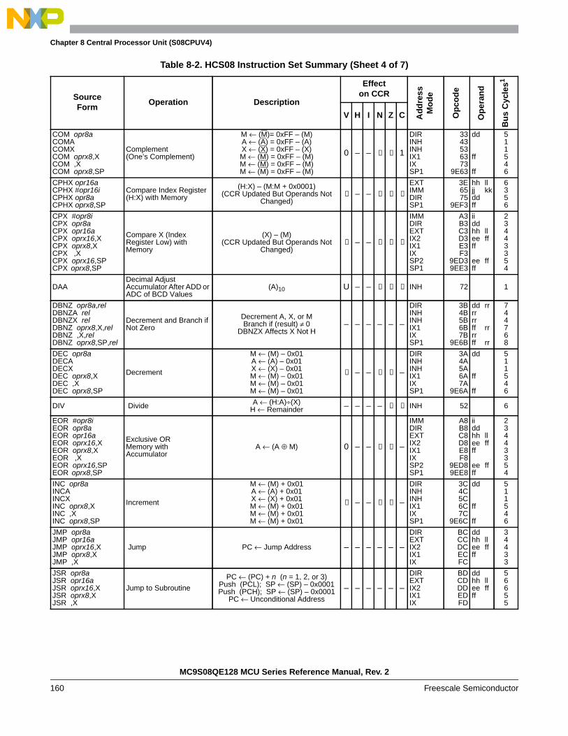
Chapter 8 Central Processor Unit (S08CPUV4)
COM opr8aCOMACOMXCOM oprx8,XCOM ,XCOM oprx8,SP
Complement(One’s Complement)
M ← (M)= 0xFF – (M)A ← (A) = 0xFF – (A)X ← (X) = 0xFF – (X)M ← (M) = 0xFF – (M)M ← (M) = 0xFF – (M)M ← (M) = 0xFF – (M)
0 – – ↕ ↕ 1
DIRINHINHIX1IXSP1
3343536373
9E63
dd
ff
ff
511546
CPHX opr16aCPHX #opr16iCPHX opr8aCPHX oprx8,SP
Compare Index Register(H:X) with Memory
(H:X) – (M:M + 0x0001)(CCR Updated But Operands Not
Changed)↕ – – ↕ ↕ ↕
EXTIMMDIRSP1
3E6575
9EF3
hh lljj kkddff
6356
CPX #opr8iCPX opr8aCPX opr16aCPX oprx16,XCPX oprx8,XCPX ,XCPX oprx16,SPCPX oprx8,SP
Compare X (IndexRegister Low) withMemory
(X) – (M)(CCR Updated But Operands Not
Changed)↕ – – ↕ ↕ ↕
IMMDIREXTIX2IX1IXSP2SP1
A3B3C3D3E3F3
9ED39EE3
iiddhh llee ffff
ee ffff
23443354
DAADecimal AdjustAccumulator After ADD orADC of BCD Values
(A)10 U – – ↕ ↕ ↕ INH 72 1
DBNZ opr8a,relDBNZA relDBNZX relDBNZ oprx8,X,relDBNZ ,X,relDBNZ oprx8,SP,rel
Decrement and Branch ifNot Zero
Decrement A, X, or MBranch if (result) ≠ 0
DBNZX Affects X Not H– – – – – –
DIRINHINHIX1IXSP1
3B4B5B6B7B
9E6B
dd rrrrrrff rrrrff rr
744768
DEC opr8aDECADECXDEC oprx8,XDEC ,XDEC oprx8,SP
Decrement
M ← (M) – 0x01A ← (A) – 0x01X ← (X) – 0x01M ← (M) – 0x01M ← (M) – 0x01M ← (M) – 0x01
↕ – – ↕ ↕ –
DIRINHINHIX1IXSP1
3A4A5A6A7A
9E6A
dd
ff
ff
511546
DIV Divide A ← (H:A)÷(X)H ← Remainder – – – – ↕ ↕ INH 52 6
EOR #opr8iEOR opr8aEOR opr16aEOR oprx16,XEOR oprx8,XEOR ,XEOR oprx16,SPEOR oprx8,SP
Exclusive ORMemory withAccumulator
A ← (A ⊕ M) 0 – – ↕ ↕ –
IMMDIREXTIX2IX1IXSP2SP1
A8B8C8D8E8F8
9ED89EE8
iiddhh llee ffff
ee ffff
23443354
INC opr8aINCAINCXINC oprx8,XINC ,XINC oprx8,SP
Increment
M ← (M) + 0x01A ← (A) + 0x01X ← (X) + 0x01M ← (M) + 0x01M ← (M) + 0x01M ← (M) + 0x01
↕ – – ↕ ↕ –
DIRINHINHIX1IXSP1
3C4C5C6C7C
9E6C
dd
ff
ff
511546
JMP opr8aJMP opr16aJMP oprx16,XJMP oprx8,XJMP ,X
Jump PC ← Jump Address – – – – – –
DIREXTIX2IX1IX
BCCCDCECFC
ddhh llee ffff
34433
JSR opr8aJSR opr16aJSR oprx16,XJSR oprx8,XJSR ,X
Jump to Subroutine
PC ← (PC) + n (n = 1, 2, or 3)Push (PCL); SP ← (SP) – 0x0001Push (PCH); SP ← (SP) – 0x0001
PC ← Unconditional Address
– – – – – –
DIREXTIX2IX1IX
BDCDDDEDFD
ddhh llee ffff
56655
Table 8-2. HCS08 Instruction Set Summary (Sheet 4 of 7)
SourceForm
Operation Description
Effecton CCR
Ad
dre
ssM
od
e
Op
cod
e
Op
eran
d
Bu
s C
ycle
s1
V H I N Z C
MC9S08QE128 MCU Series Reference Manual, Rev. 2
160 Freescale Semiconductor

Chapter 8 Central Processor Unit (S08CPUV4)
LDA #opr8iLDA opr8aLDA opr16aLDA oprx16,XLDA oprx8,XLDA ,XLDA oprx16,SPLDA oprx8,SP
Load Accumulator fromMemory A ← (M) 0 – – ↕ ↕ –
IMMDIREXTIX2IX1IXSP2SP1
A6B6C6D6E6F6
9ED69EE6
iiddhh llee ffff
ee ffff
23443354
LDHX #opr16iLDHX opr8aLDHX opr16aLDHX ,XLDHX oprx16,XLDHX oprx8,XLDHX oprx8,SP
Load Index Register (H:X)from Memory H:X ← (M:M + 0x0001) 0 – – ↕ ↕ –
IMMDIREXTIXIX2IX1SP1
455532
9EAE9EBE9ECE9EFE
jj kkddhh ll
ee ffffff
3455655
LDX #opr8iLDX opr8aLDX opr16aLDX oprx16,XLDX oprx8,XLDX ,XLDX oprx16,SPLDX oprx8,SP
Load X (Index RegisterLow) from Memory X ← (M) 0 – – ↕ ↕ –
IMMDIREXTIX2IX1IXSP2SP1
AEBECEDEEEFE
9EDE9EEE
iiddhh llee ffff
ee ffff
23443354
LSL opr8aLSLALSLXLSL oprx8,XLSL ,XLSL oprx8,SP
Logical Shift Left(Same as ASL) ↕ – – ↕ ↕ ↕
DIRINHINHIX1IXSP1
3848586878
9E68
dd
ff
ff
511546
LSR opr8aLSRALSRXLSR oprx8,XLSR ,XLSR oprx8,SP
Logical Shift Right ↕ – – 0 ↕ ↕
DIRINHINHIX1IXSP1
3444546474
9E64
dd
ff
ff
511546
MOV opr8a,opr8aMOV opr8a,X+MOV #opr8i,opr8aMOV ,X+,opr8a
Move
(M)destination ← (M)source
H:X ← (H:X) + 0x0001 inIX+/DIR and DIR/IX+ Modes
0 – – ↕ ↕ –DIR/DIRDIR/IX+IMM/DIRIX+/DIR
4E5E6E7E
dd ddddii dddd
5545
MUL Unsigned multiply X:A ← (X) × (A) – 0 – – – 0 INH 42 5
NEG opr8aNEGANEGXNEG oprx8,XNEG ,XNEG oprx8,SP
Negate(Two’s Complement)
M ← – (M) = 0x00 – (M)A ← – (A) = 0x00 – (A)X ← – (X) = 0x00 – (X)M ← – (M) = 0x00 – (M)M ← – (M) = 0x00 – (M)M ← – (M) = 0x00 – (M)
– – ↕ ↕ ↕
DIRINHINHIX1IXSP1
3040506070
9E60
dd
ff
ff
511546
NOP No Operation Uses 1 Bus Cycle – – – – – – INH 9D 1
NSA Nibble SwapAccumulator A ← (A[3:0]:A[7:4]) – – – – – – INH 62 1
ORA #opr8iORA opr8aORA opr16aORA oprx16,XORA oprx8,XORA ,XORA oprx16,SPORA oprx8,SP
Inclusive OR Accumulatorand Memory A ← (A) | (M) 0 – – ↕ ↕ –
IMMDIREXTIX2IX1IXSP2SP1
AABACADAEAFA
9EDA9EEA
iiddhh llee ffff
ee ffff
23443354
PSHA Push Accumulator ontoStack Push (A); SP ← (SP) – 0x0001 – – – – – – INH 87 2
PSHH Push H (Index RegisterHigh) onto Stack Push (H); SP ← (SP) – 0x0001 – – – – – – INH 8B 2
PSHX Push X (Index RegisterLow) onto Stack Push (X); SP ← (SP) – 0x0001 – – – – – – INH 89 2
Table 8-2. HCS08 Instruction Set Summary (Sheet 5 of 7)
SourceForm
Operation Description
Effecton CCR
Ad
dre
ssM
od
e
Op
cod
e
Op
eran
d
Bu
s C
ycle
s1
V H I N Z C
C
b0b7
0
b0b7
C0
MC9S08QE128 MCU Series Reference Manual, Rev. 2
Freescale Semiconductor 161

Chapter 8 Central Processor Unit (S08CPUV4)
PULA Pull Accumulator fromStack SP ← (SP + 0x0001); Pull (A) – – – – – – INH 86 3
PULH Pull H (Index RegisterHigh) from Stack SP ← (SP + 0x0001); Pull (H) – – – – – – INH 8A 3
PULX Pull X (Index RegisterLow) from Stack SP ← (SP + 0x0001); Pull (X) – – – – – – INH 88 3
ROL opr8aROLAROLXROL oprx8,XROL ,XROL oprx8,SP
Rotate Left through Carry ↕ – – ↕ ↕ ↕
DIRINHINHIX1IXSP1
3949596979
9E69
dd
ff
ff
511546
ROR opr8aRORARORXROR oprx8,XROR ,XROR oprx8,SP
Rotate Right throughCarry ↕ – – ↕ ↕ ↕
DIRINHINHIX1IXSP1
3646566676
9E66
dd
ff
ff
511546
RSP Reset Stack Pointer SP ← 0xFF(High Byte Not Affected) – – – – – – INH 9C 1
RTC Return fom CALLSP ← (SP) + 0x0001; Pull (PPAGE)
SP ← (SP) + 0x0001; Pull (PCH)SP ← (SP) + 0x0001; Pull (PCL)
– – – – – – INH 8D 7
RTI Return from Interrupt
SP ← (SP) + 0x0001; Pull (CCR)SP ← (SP) + 0x0001; Pull (A)SP ← (SP) + 0x0001; Pull (X)
SP ← (SP) + 0x0001; Pull (PCH)SP ← (SP) + 0x0001; Pull (PCL)
↕ ↕ ↕ ↕ ↕ ↕ INH 80 9
RTS Return from Subroutine SP ← SP + 0x0001; Pull (PCH)SP ← SP + 0x0001; Pull (PCL) – – – – – – INH 81 6
SBC #opr8iSBC opr8aSBC opr16aSBC oprx16,XSBC oprx8,XSBC ,XSBC oprx16,SPSBC oprx8,SP
Subtract with Carry A ← (A) – (M) – (C) ↕ – – ↕ ↕ ↕
IMMDIREXTIX2IX1IXSP2SP1
A2B2C2D2E2F2
9ED29EE2
iiddhh llee ffff
ee ffff
23443354
SEC Set Carry Bit C ← 1 – – – – – 1 INH 99 1
SEI Set Interrupt Mask Bit I ← 1 – – 1 – – – INH 9B 1
STA opr8aSTA opr16aSTA oprx16,XSTA oprx8,XSTA ,XSTA oprx16,SPSTA oprx8,SP
Store Accumulator inMemory M ← (A) 0 – – ↕ ↕ –
DIREXTIX2IX1IXSP2SP1
B7C7D7E7F7
9ED79EE7
ddhh llee ffff
ee ffff
3443254
STHX opr8aSTHX opr16aSTHX oprx8,SP
Store H:X (Index Reg.) (M:M + 0x0001) ← (H:X) 0 – – ↕ ↕ –DIREXTSP1
3596
9EFF
ddhh llff
455
STOP
Enable Interrupts:Stop ProcessingRefer to MCUDocumentation
I bit ← 0; Stop Processing – – 0 – – – INH 8E 2+
STX opr8aSTX opr16aSTX oprx16,XSTX oprx8,XSTX ,XSTX oprx16,SPSTX oprx8,SP
Store X (Low 8 Bits ofIndex Register)in Memory
M ← (X) 0 – – ↕ ↕ –
DIREXTIX2IX1IXSP2SP1
BFCFDFEFFF
9EDF9EEF
ddhh llee ffff
ee ffff
3443254
Table 8-2. HCS08 Instruction Set Summary (Sheet 6 of 7)
SourceForm
Operation Description
Effecton CCR
Ad
dre
ssM
od
e
Op
cod
e
Op
eran
d
Bu
s C
ycle
s1
V H I N Z C
C
b0b7
b0b7
C
MC9S08QE128 MCU Series Reference Manual, Rev. 2
162 Freescale Semiconductor

Chapter 8 Central Processor Unit (S08CPUV4)
SUB #opr8iSUB opr8aSUB opr16aSUB oprx16,XSUB oprx8,XSUB ,XSUB oprx16,SPSUB oprx8,SP
Subtract A ← (A) – (M) ↕ – – ↕ ↕ ↕
IMMDIREXTIX2IX1IXSP2SP1
A0B0C0D0E0F0
9ED09EE0
iiddhh llee ffff
ee ffff
23443354
SWI Software Interrupt
PC ← (PC) + 0x0001Push (PCL); SP ← (SP) – 0x0001Push (PCH); SP ← (SP) – 0x0001
Push (X); SP ← (SP) – 0x0001Push (A); SP ← (SP) – 0x0001
Push (CCR); SP ← (SP) – 0x0001I ← 1;
PCH ← Interrupt Vector High BytePCL ← Interrupt Vector Low Byte
– – 1 – – – INH 83 11
TAP Transfer Accumulator toCCR CCR ← (A) ↕ ↕ ↕ ↕ ↕ ↕ INH 84 1
TAX Transfer Accumulator toX (Index Register Low) X ← (A) – – – – – – INH 97 1
TPA Transfer CCR toAccumulator A ← (CCR) – – – – – – INH 85 1
TST opr8aTSTATSTXTST oprx8,XTST ,XTST oprx8,SP
Test for Negative or Zero
(M) – 0x00(A) – 0x00(X) – 0x00(M) – 0x00(M) – 0x00(M) – 0x00
0 – – ↕ ↕ –
DIRINHINHIX1IXSP1
3D4D5D6D7D
9E6D
dd
ff
ff
411435
TSX Transfer SP to Index Reg. H:X ← (SP) + 0x0001 – – – – – – INH 95 2
TXA Transfer X (Index Reg.Low) to Accumulator A ← (X) – – – – – – INH 9F 1
TXS Transfer Index Reg. to SP SP ← (H:X) – 0x0001 – – – – – – INH 94 2
WAIT Enable Interrupts; Waitfor Interrupt I bit ← 0; Halt CPU – – 0 – – – INH 8F 2+
1 Bus clock frequency is one-half of the CPU clock frequency.
Table 8-2. HCS08 Instruction Set Summary (Sheet 7 of 7)
SourceForm
Operation Description
Effecton CCR
Ad
dre
ssM
od
e
Op
cod
e
Op
eran
d
Bu
s C
ycle
s1
V H I N Z C
MC9S08QE128 MCU Series Reference Manual, Rev. 2
Freescale Semiconductor 163
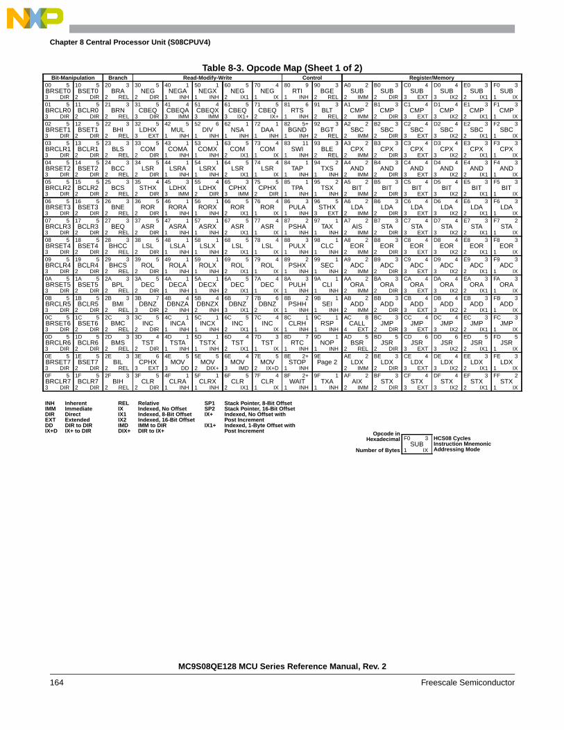
Chapter 8 Central Processor Unit (S08CPUV4)
Table 8-3. Opcode Map (Sheet 1 of 2)Bit-Manipulation Branch Read-Modify-Write Control Register/Memory
00 5BRSET03 DIR
10 5BSET0
2 DIR
20 3BRA
2 REL
30 5NEG
2 DIR
40 1NEGA
1 INH
50 1NEGX
1 INH
60 5NEG
2 IX1
70 4NEG
1 IX
80 9RTI
1 INH
90 3BGE
2 REL
A0 2SUB
2 IMM
B0 3SUB
2 DIR
C0 4SUB
3 EXT
D0 4SUB
3 IX2
E0 3SUB
2 IX1
F0 3SUB
1 IX01 5BRCLR03 DIR
11 5BCLR0
2 DIR
21 3BRN
2 REL
31 5CBEQ
3 DIR
41 4CBEQA
3 IMM
51 4CBEQX
3 IMM
61 5CBEQ
3 IX1+
71 5CBEQ
2 IX+
81 6RTS
1 INH
91 3BLT
2 REL
A1 2CMP
2 IMM
B1 3CMP
2 DIR
C1 4CMP
3 EXT
D1 4CMP
3 IX2
E1 3CMP
2 IX1
F1 3CMP
1 IX02 5BRSET13 DIR
12 5BSET1
2 DIR
22 3BHI
2 REL
32 5LDHX
3 EXT
42 5MUL
1 INH
52 6DIV
1 INH
62 1NSA
1 INH
72 1DAA
1 INH
82 5+BGND
1 INH
92 3BGT
2 REL
A2 2SBC
2 IMM
B2 3SBC
2 DIR
C2 4SBC
3 EXT
D2 4SBC
3 IX2
E2 3SBC
2 IX1
F2 3SBC
1 IX03 5BRCLR13 DIR
13 5BCLR1
2 DIR
23 3BLS
2 REL
33 5COM
2 DIR
43 1COMA
1 INH
53 1COMX
1 INH
63 5COM
2 IX1
73 4COM
1 IX
83 11SWI
1 INH
93 3BLE
2 REL
A3 2CPX
2 IMM
B3 3CPX
2 DIR
C3 4CPX
3 EXT
D3 4CPX
3 IX2
E3 3CPX
2 IX1
F3 3CPX
1 IX04 5BRSET23 DIR
14 5BSET2
2 DIR
24 3BCC
2 REL
34 5LSR
2 DIR
44 1LSRA
1 INH
54 1LSRX
1 INH
64 5LSR
2 IX1
74 4LSR
1 IX
84 1TAP
1 INH
94 2TXS
1 INH
A4 2AND
2 IMM
B4 3AND
2 DIR
C4 4AND
3 EXT
D4 4AND
3 IX2
E4 3AND
2 IX1
F4 3AND
1 IX05 5BRCLR23 DIR
15 5BCLR2
2 DIR
25 3BCS
2 REL
35 4STHX
2 DIR
45 3LDHX
3 IMM
55 4LDHX
2 DIR
65 3CPHX
3 IMM
75 5CPHX
2 DIR
85 1TPA
1 INH
95 2TSX
1 INH
A5 2BIT
2 IMM
B5 3BIT
2 DIR
C5 4BIT
3 EXT
D5 4BIT
3 IX2
E5 3BIT
2 IX1
F5 3BIT
1 IX06 5BRSET33 DIR
16 5BSET3
2 DIR
26 3BNE
2 REL
36 5ROR
2 DIR
46 1RORA
1 INH
56 1RORX
1 INH
66 5ROR
2 IX1
76 4ROR
1 IX
86 3PULA
1 INH
96 5STHX
3 EXT
A6 2LDA
2 IMM
B6 3LDA
2 DIR
C6 4LDA
3 EXT
D6 4LDA
3 IX2
E6 3LDA
2 IX1
F6 3LDA
1 IX07 5BRCLR33 DIR
17 5BCLR3
2 DIR
27 3BEQ
2 REL
37 5ASR
2 DIR
47 1ASRA
1 INH
57 1ASRX
1 INH
67 5ASR
2 IX1
77 4ASR
1 IX
87 2PSHA
1 INH
97 1TAX
1 INH
A7 2AIS
2 IMM
B7 3STA
2 DIR
C7 4STA
3 EXT
D7 4STA
3 IX2
E7 3STA
2 IX1
F7 2STA
1 IX08 5BRSET43 DIR
18 5BSET4
2 DIR
28 3BHCC
2 REL
38 5LSL
2 DIR
48 1LSLA
1 INH
58 1LSLX
1 INH
68 5LSL
2 IX1
78 4LSL
1 IX
88 3PULX
1 INH
98 1CLC
1 INH
A8 2EOR
2 IMM
B8 3EOR
2 DIR
C8 4EOR
3 EXT
D8 4EOR
3 IX2
E8 3EOR
2 IX1
F8 3EOR
1 IX09 5BRCLR43 DIR
19 5BCLR4
2 DIR
29 3BHCS
2 REL
39 5ROL
2 DIR
49 1ROLA
1 INH
59 1ROLX
1 INH
69 5ROL
2 IX1
79 4ROL
1 IX
89 2PSHX
1 INH
99 1SEC
1 INH
A9 2ADC
2 IMM
B9 3ADC
2 DIR
C9 4ADC
3 EXT
D9 4ADC
3 IX2
E9 3ADC
2 IX1
F9 3ADC
1 IX0A 5BRSET53 DIR
1A 5BSET5
2 DIR
2A 3BPL
2 REL
3A 5DEC
2 DIR
4A 1DECA
1 INH
5A 1DECX
1 INH
6A 5DEC
2 IX1
7A 4DEC
1 IX
8A 3PULH
1 INH
9A 1CLI
1 INH
AA 2ORA
2 IMM
BA 3ORA
2 DIR
CA 4ORA
3 EXT
DA 4ORA
3 IX2
EA 3ORA
2 IX1
FA 3ORA
1 IX0B 5BRCLR53 DIR
1B 5BCLR5
2 DIR
2B 3BMI
2 REL
3B 7DBNZ
3 DIR
4B 4DBNZA
2 INH
5B 4DBNZX
2 INH
6B 7DBNZ
3 IX1
7B 6DBNZ
2 IX
8B 2PSHH
1 INH
9B 1SEI
1 INH
AB 2ADD
2 IMM
BB 3ADD
2 DIR
CB 4ADD
3 EXT
DB 4ADD
3 IX2
EB 3ADD
2 IX1
FB 3ADD
1 IX0C 5BRSET63 DIR
1C 5BSET6
2 DIR
2C 3BMC
2 REL
3C 5INC
2 DIR
4C 1INCA
1 INH
5C 1INCX
1 INH
6C 5INC
2 IX1
7C 4INC
1 IX
8C 1CLRH
1 INH
9C 1RSP
1 INH
AC 8CALL
4 EXT
BC 3JMP
2 DIR
CC 4JMP
3 EXT
DC 4JMP
3 IX2
EC 3JMP
2 IX1
FC 3JMP
1 IX0D 5BRCLR63 DIR
1D 5BCLR6
2 DIR
2D 3BMS
2 REL
3D 4TST
2 DIR
4D 1TSTA
1 INH
5D 1TSTX
1 INH
6D 4TST
2 IX1
7D 3TST
1 IX
8D 7RTC
1 INH
9D 1NOP
1 INH
AD 5BSR
2 REL
BD 5JSR
2 DIR
CD 6JSR
3 EXT
DD 6JSR
3 IX2
ED 5JSR
2 IX1
FD 5JSR
1 IX0E 5BRSET73 DIR
1E 5BSET7
2 DIR
2E 3BIL
2 REL
3E 6CPHX
3 EXT
4E 5MOV
3 DD
5E 5MOV
2 DIX+
6E 4MOV
3 IMD
7E 5MOV
2 IX+D
8E 2+STOP
1 INH
9EPage 2
AE 2LDX
2 IMM
BE 3LDX
2 DIR
CE 4LDX
3 EXT
DE 4LDX
3 IX2
EE 3LDX
2 IX1
FE 3LDX
1 IX0F 5BRCLR73 DIR
1F 5BCLR7
2 DIR
2F 3BIH
2 REL
3F 5CLR
2 DIR
4F 1CLRA
1 INH
5F 1CLRX
1 INH
6F 5CLR
2 IX1
7F 4CLR
1 IX
8F 2+WAIT
1 INH
9F 1TXA
1 INH
AF 2AIX
2 IMM
BF 3STX
2 DIR
CF 4STX
3 EXT
DF 4STX
3 IX2
EF 3STX
2 IX1
FF 2STX
1 IX
INH Inherent REL Relative SP1 Stack Pointer, 8-Bit OffsetIMM Immediate IX Indexed, No Offset SP2 Stack Pointer, 16-Bit OffsetDIR Direct IX1 Indexed, 8-Bit Offset IX+ Indexed, No Offset withEXT Extended IX2 Indexed, 16-Bit Offset Post IncrementDD DIR to DIR IMD IMM to DIR IX1+ Indexed, 1-Byte Offset withIX+D IX+ to DIR DIX+ DIR to IX+ Post Increment Opcode in
Hexadecimal
Number of Bytes
F0 3SUB
1 IX
HCS08 CyclesInstruction MnemonicAddressing Mode
MC9S08QE128 MCU Series Reference Manual, Rev. 2
164 Freescale Semiconductor
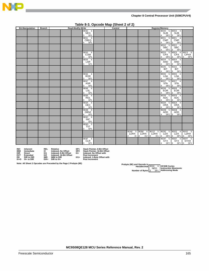
Chapter 8 Central Processor Unit (S08CPUV4)
Bit-Manipulation Branch Read-Modify-Write Control Register/Memory9E60 6
NEG3 SP1
9ED0 5SUB
4 SP2
9EE0 4SUB
3 SP19E61 6
CBEQ4 SP1
9ED1 5CMP
4 SP2
9EE1 4CMP
3 SP19ED2 5
SBC4 SP2
9EE2 4SBC
3 SP19E63 6
COM3 SP1
9ED3 5CPX
4 SP2
9EE3 4CPX
3 SP1
9EF3 6CPHX
3 SP19E64 6
LSR3 SP1
9ED4 5AND
4 SP2
9EE4 4AND
3 SP19ED5 5
BIT4 SP2
9EE5 4BIT
3 SP19E66 6
ROR3 SP1
9ED6 5LDA
4 SP2
9EE6 4LDA
3 SP19E67 6
ASR3 SP1
9ED7 5STA
4 SP2
9EE7 4STA
3 SP19E68 6
LSL3 SP1
9ED8 5EOR
4 SP2
9EE8 4EOR
3 SP19E69 6
ROL3 SP1
9ED9 5ADC
4 SP2
9EE9 4ADC
3 SP19E6A 6
DEC3 SP1
9EDA 5ORA
4 SP2
9EEA 4ORA
3 SP19E6B 8
DBNZ4 SP1
9EDB 5ADD
4 SP2
9EEB 4ADD
3 SP19E6C 6
INC3 SP19E6D 5
TST3 SP1
9EAE 5LDHX
2 IX
9EBE 6LDHX
4 IX2
9ECE 5LDHX
3 IX1
9EDE 5LDX
4 SP2
9EEE 4LDX
3 SP1
9EFE 5LDHX
3 SP19E6F 6
CLR3 SP1
9EDF 5STX
4 SP2
9EEF 4STX
3 SP1
9EFF 5STHX
3 SP1
INH Inherent REL Relative SP1 Stack Pointer, 8-Bit OffsetIMM Immediate IX Indexed, No Offset SP2 Stack Pointer, 16-Bit OffsetDIR Direct IX1 Indexed, 8-Bit Offset IX+ Indexed, No Offset withEXT Extended IX2 Indexed, 16-Bit Offset Post IncrementDD DIR to DIR IMD IMM to DIR IX1+ Indexed, 1-Byte Offset withIX+D IX+ to DIR DIX+ DIR to IX+ Post Increment
Note: All Sheet 2 Opcodes are Preceded by the Page 2 Prebyte (9E) Prebyte (9E) and Opcode inHexadecimal
Number of Bytes
9E60 6NEG
3 SP1
HCS08 CyclesInstruction MnemonicAddressing Mode
Table 8-3. Opcode Map (Sheet 2 of 2)
MC9S08QE128 MCU Series Reference Manual, Rev. 2
Freescale Semiconductor 165

Chapter 8 Central Processor Unit (S08CPUV4)
MC9S08QE128 MCU Series Reference Manual, Rev. 2
166 Freescale Semiconductor

Chapter 9Analog Comparator 3V (ACMPVLPV1)
9.1 IntroductionMC9S08QE128 Series MCUs have two independent analog comparators (ACMPs), named ACMP1 andACMP2.
The analog comparator module (ACMP) provides a circuit for comparing two analog input voltages or forcomparing one analog input voltage to an internal reference voltage. The comparator circuit is designed tooperate across the full range of the supply voltage (rail-to-rail operation).
Figure 9-1 shows the MC9S08QE128 Series block diagram with the ACMP highlighted.
NOTEIgnore any references to stop1 low-power mode in this chapter, because theMC9S08QE128 device does not support it.
9.1.1 ACMP Configuration Information
When using the bandgap reference voltage for input to ACMP1+ and/or ACMP2+, the user must enablethe bandgap buffer by setting SPMS[BGBE]. For value of bandgap voltage reference see the data sheet.
9.1.2 ACMP/TPM Configuration Information
The ACMP modules can be configured to connect the output of the analog comparator to a TPM inputcapture channel 0 by setting the corresponding ACICx bit in SOPT2. With ACICx set, the TPMxCH0 pinis not available externally regardless of the configuration of the TPMx module.
The ACMP1 output can be connected to TPM1CH0; The ACMP2 output can be connected to TPM2CH0.
9.1.3 ACMP Clock Gating
The bus clock to both of the ACMPs can be gated on and off using the SCGC2[ACMP] bit. This bit is setafter any reset, which enables the bus clock to this module. To conserve power, the ACMP bit can becleared to disable the clock to this module when not in use. See Section 5.7, “Peripheral Clock Gating,”for details.
MC9S08QE128 MCU Series Reference Manual, Rev. 2
Freescale Semiconductor 167

Chapter 9 Analog Comparator 3V (ACMPVLPV1)
9.1.4 Interrupt Vectors
ACMP1 and ACMP2 share a single interrupt vector. When interrupts are enabled for both ACMPs, theACF bit in ACMP1SC and ACMP2SC must be polled to determine which ACMP caused the interrupt. SeeSection 4.2, “Reset and Interrupt Vector Assignments,” for the ACMP interrupt vector assignment.
MC9S08QE128 MCU Series Reference Manual, Rev. 2
168 Freescale Semiconductor

Chapter 9 Analog Comparator 3V (ACMPVLPV1)
-+
Figure 9-1. MC9S08QE128 Series Block Diagram Highlighting ACMP Block and Pins
TPM2CH2-TPM2CH0
TPM1CH0
TPM1CH2-
VSS
VDD
IIC MODULE (IIC1)
SERIAL PERIPHERAL INTERFACE MODULE (SPI1)
USER FLASH
USER RAM
128K / 96K / 64K
HCS08 CORE
CPU
BDC
6-CHANNEL TIMER/PWMMODULE (TPM3)
HCS08 SYSTEM CONTROL
RESETS AND INTERRUPTSMODES OF OPERATIONPOWER MANAGEMENT
VOLTAGEREGULATOR
COP
IRQ
LVD
OSCILLATOR (XOSC)
RES
ET
VREFL
VREFH
8K / 6K / 4K
BKG
D/M
S
INTERFACE (SCI1)SERIAL COMMUNICATIONS
MISO1SS1
SPSCK1
3-CHANNEL TIMER/PWMMODULE (TPM2)
REAL TIME COUNTER (RTC)
DEBUG MODULE (DBG)
IRQ
PTA3/KBI1P3/SCL1/ADP3
PTA5/IRQ/TPM1CLK/RESET
PTA2/KBI1P2/SDA1/ADP2
PTA6/TPM1CH2/ADP8PTA7/TPM2CH2/ADP9
MOSI1
PTB3/KBI1P7/MOSI1/ADP7PTB4/TPM2CH1/MISO1PTB5/TPM1CH1/SS1
PTB2/KBI1P6/SPSCK1/ADP6PTB1/KBI1P5/TxD1/ADP5PTB0/KBI1P4/RxD1/ADP4
PORT
B
PTB6/SDA1/XTALPTB7/SCL1/EXTAL
PTC3/TPM3CH3PTC4/TPM3CH4/RSTO
PTC2/TPM3CH2PTC1/TPM3CH1PTC0/TPM3CH0
PTD3/KBI2P3/SS2PTD4/KBI2P4PTD5/KBI2P5
PTD2/KBI2P2/MISO2PTD1/KBI2P1/MOSI2PTD0/KBI2P0/SPSCK2
PORT
D
PTD6/KBI2P6PTD7/KBI2P7
PTE3/SS1PTE4PTE5
PTE2/MISO1PTE1/MOSI1
TPM2CLK
PORT
EPTE6
PTE0/TPM2CLK/SPSCK1
PTF3/ADP13PTF4/ADP14PTF5/ADP15
PTF2/ADP12PTF1/ADP11PTF0/ADP10
PORT
F
PTF6/ADP16PTF7/ADP17
PTG1PTG2/ADP18PTG3/ADP19PO
RT G
PTG4/ADP20PTG5/ADP21
PTG0
VSS
VDD
VSSA
VDDA
BKP
INT
INTERFACE (SCI2)SERIAL COMMUNICATIONS
6TPM3CH5 -TPM3CH0
- VREFH/VREFL internally connected to VDDA/VSSA in 48-pin and 32-pin packages- VDD and VSS pins are each internally connected to two pads in 32-pin package
PTG6/ADP22PTG7/ADP23
SOURCE (ICS)INTERNAL CLOCK
RES
ET
PORT
JPO
RT H
PTJ1PTJ2PTJ3PTJ4PTJ5
PTJ0
PTJ6PTJ7
PTH1PTH2PTH3PTH4PTH5
PTH0
PTH6/SCL2PTH7/SDA2
IIC MODULE (IIC2)
ANALOG-TO-DIGITALCONVERTER (ADC)
24-CHANNEL,12-BIT
3-CHANNEL TIMER/PWMMODULE (TPM1)
SDA2SCL2
SERIAL PERIPHERAL INTERFACE MODULE (SPI2)
MISO2SS2
SPSCK2MOSI2
EXTALXTAL
10
SDA1SCL1
RxD1TxD1
RxD2TxD2
TPM3CLK
3
TPM1CLK
PTE7/TPM3CLK
ANALOG COMPARATOR(ACMP1)
ACMP1O
ACMP1-ACMP1+
PTA4/ACMP1O/BKGD/MS
PTA1/KBI1P1/TPM2CH0/ADP1/ACMP1PTA0/KBI1P0/TPM1CH0/ADP0/ACMP1
PORT
A
PTC5/TPM3CH5/ACMP2O
PORT
C
PTC6/RxD2/ACMP2+PTC7/TxD2/ACMP2-
ANALOG COMPARATOR(ACMP2) ACMP2-
ACMP2+ACMP2O
MC9S08QE128 MCU Series Reference Manual, Rev. 2
Freescale Semiconductor 169

Analog Comparator (S08ACMPV3)
9.1.5 Features
The ACMP has the following features:
• Full rail to rail supply operation.
• Selectable interrupt on rising edge, falling edge, or either rising or falling edges of comparatoroutput.
• Option to compare to fixed internal bandgap reference voltage.
• Option to allow comparator output to be visible on a pin, ACMPxO.
9.1.6 Modes of Operation
This section defines the ACMP operation in wait, stop and background debug modes.
9.1.6.1 ACMP in Wait Mode
The ACMP continues to run in wait mode if enabled before executing the WAIT instruction. Therefore,the ACMP can be used to bring the MCU out of wait mode if the ACMP interrupt, ACIE is enabled. Forlowest possible current consumption, the ACMP should be disabled by software if not required as aninterrupt source during wait mode.
9.1.6.2 ACMP in Stop Modes
The ACMP is disabled in all stop modes, regardless of the settings before executing the STOP instruction.Therefore, the ACMP cannot be used as a wake up source from stop modes.
During either stop1 or stop2 mode, the ACMP module will be fully powered down. Upon wake-up fromstop1 or stop2 mode, the ACMP module will be in the reset state.
During stop3 mode, clocks to the ACMP module are halted. No registers are affected. In addition, theACMP comparator circuit will enter a low power state. No compare operation will occur while in stop3.
If stop3 is exited with a reset, the ACMP will be put into its reset state. If stop3 is exited with an interrupt,the ACMP continues from the state it was in when stop3 was entered.
9.1.6.3 ACMP in Active Background Mode
When the microcontroller is in active background mode, the ACMP will continue to operate normally.
9.1.7 Block Diagram
The block diagram for the Analog Comparator module is shown Figure 9-2.
MC9S08QE128 MCU Series Reference Manual, Rev. 2
170 Freescale Semiconductor

Analog Comparator (S08ACMPV3)
Figure 9-2. Analog Comparator (ACMP) Block Diagram
9.2 External Signal DescriptionThe ACMP has two analog input pins, ACMPx+ and ACMPx- and one digital output pin ACMPxO. Eachof these pins can accept an input voltage that varies across the full operating voltage range of the MCU.As shown in Figure 9-2, the ACMPx- pin is connected to the inverting input of the comparator, and theACMPx+ pin is connected to the comparator non-inverting input if ACBGS is a 0. As shown in Figure 9-2,the ACMPxO pin can be enabled to drive an external pin.
The signal properties of ACMP are shown in Table 9-1.
9.3 Register DefinitionThe ACMP includes one register:
• An 8-bit status and control register
Table 9-1. Signal Properties
Signal Function I/O
ACMPx- Inverting analog input to the ACMP. (Minus input) I
ACMPx+ Non-inverting analog input to the ACMP. (Positive input) I
ACMPxO Digital output of the ACMP. O
+
-
InterruptControl
InternalReference
ACBGS
Internal Bus
Status & ControlRegister
AC
MO
D
set A
CF
ACME ACF
ACIE
ACOPE
Comparator
ACMPxINTERRUPTREQUEST
ACMPx+
ACMPx-
ACMPxO
MC9S08QE128 MCU Series Reference Manual, Rev. 2
Freescale Semiconductor 171
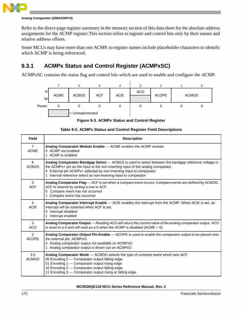
Analog Comparator (S08ACMPV3)
Refer to the direct-page register summary in the memory section of this data sheet for the absolute addressassignments for the ACMP register.This section refers to register and control bits only by their names andrelative address offsets.
Some MCUs may have more than one ACMP, so register names include placeholder characters to identifywhich ACMP is being referenced.
9.3.1 ACMPx Status and Control Register (ACMPxSC)
ACMPxSC contains the status flag and control bits which are used to enable and configure the ACMP.
7 6 5 4 3 2 1 0
RACME ACBGS ACF ACIE
ACOACOPE ACMOD
W
Reset: 0 0 0 0 0 0 0 0
= Unimplemented
Figure 9-3. ACMPx Status and Control Register
Table 9-2. ACMPx Status and Control Register Field Descriptions
Field Description
7ACME
Analog Comparator Module Enable — ACME enables the ACMP module.0 ACMP not enabled1 ACMP is enabled
6ACBGS
Analog Comparator Bandgap Select — ACBGS is used to select between the bandgap reference voltage orthe ACMPx+ pin as the input to the non-inverting input of the analog comparator.0 External pin ACMPx+ selected as non-inverting input to comparator1 Internal reference select as non-inverting input to comparator
5ACF
Analog Comparator Flag — ACF is set when a compare event occurs. Compare events are defined by ACMOD.ACF is cleared by writing a one to ACF.0 Compare event has not occurred1 Compare event has occurred
4ACIE
Analog Comparator Interrupt Enable — ACIE enables the interrupt from the ACMP. When ACIE is set, aninterrupt will be asserted when ACF is set.0 Interrupt disabled1 Interrupt enabled
3ACO
Analog Comparator Output — Reading ACO will return the current value of the analog comparator output. ACOis reset to a 0 and will read as a 0 when the ACMP is disabled (ACME = 0).
2ACOPE
Analog Comparator Output Pin Enable — ACOPE is used to enable the comparator output to be placed ontothe external pin, ACMPxO.0 Analog comparator output not available on ACMPxO1 Analog comparator output is driven out on ACMPxO
1:0ACMOD
Analog Comparator Mode — ACMOD selects the type of compare event which sets ACF.00 Encoding 0 — Comparator output falling edge01 Encoding 1 — Comparator output rising edge10 Encoding 2 — Comparator output falling edge11 Encoding 3 — Comparator output rising or falling edge
MC9S08QE128 MCU Series Reference Manual, Rev. 2
172 Freescale Semiconductor
Analog Comparator (S08ACMPV3)
9.4 Functional DescriptionThe analog comparator can be used to compare two analog input voltages applied to ACMPx+ andACMPx-; or it can be used to compare an analog input voltage applied to ACMPx- with an internalbandgap reference voltage. ACBGS is used to select between the bandgap reference voltage or theACMPx+ pin as the input to the non-inverting input of the analog comparator. The comparator output ishigh when the non-inverting input is greater than the inverting input, and is low when the non-invertinginput is less than the inverting input. ACMOD is used to select the condition which will cause ACF to beset. ACF can be set on a rising edge of the comparator output, a falling edge of the comparator output, oreither a rising or a falling edge (toggle). The comparator output can be read directly through ACO. Thecomparator output can be driven onto the ACMPxO pin using ACOPE.
MC9S08QE128 MCU Series Reference Manual, Rev. 2
Freescale Semiconductor 173

Analog Comparator (S08ACMPV3)
MC9S08QE128 MCU Series Reference Manual, Rev. 2
174 Freescale Semiconductor
Chapter 10Analog-to-Digital Converter (S08ADC12V1)
10.1 IntroductionThe 12-bit analog-to-digital converter (ADC) is a successive approximation ADC designed for operationwithin an integrated microcontroller system-on-chip.
Figure 10-1 shows the MC9S08QE128 Series with the ADC module and pins highlighted.
NOTEIgnore any references to stop1 low-power mode in this chapter, because theMC9S08QE128 device does not support it.
10.1.1 ADC Clock Gating
The bus clock to the ADC can be gated on and off using the SCGC1[ADC] bit. This bit is set after anyreset, which enables the bus clock to this module. To conserve power, the ADC bit can be cleared to disablethe clock to this module when not in use. See Section 5.7, “Peripheral Clock Gating,” for details.
MC9S08QE128 MCU Series Reference Manual, Rev. 2
Freescale Semiconductor 175

Chapter 10 Analog-to-Digital Converter (S08ADC12V1)
-+
Figure 10-1. MC9S08QE128 Series Block Diagram Highlighting ADC Block and Pins
TPM2CH2-TPM2CH0
TPM1CH0
TPM1CH2-
ANALOG COMPARATOR(ACMP1)
ACMP1O
ACMP1-ACMP1+
VSS
VDD
IIC MODULE (IIC1)
SERIAL PERIPHERAL INTERFACE MODULE (SPI1)
USER FLASH
USER RAM
128K / 96K / 64K
HCS08 CORE
CPU
BDC
6-CHANNEL TIMER/PWMMODULE (TPM3)
HCS08 SYSTEM CONTROL
RESETS AND INTERRUPTSMODES OF OPERATIONPOWER MANAGEMENT
VOLTAGEREGULATOR
COP
IRQ
LVD
OSCILLATOR (XOSC)
RES
ET
VREFL
VREFH
8K / 6K / 4K
BKG
D/M
S
INTERFACE (SCI1)SERIAL COMMUNICATIONS
MISO1SS1
SPSCK1
3-CHANNEL TIMER/PWMMODULE (TPM2)
REAL TIME COUNTER (RTC)
DEBUG MODULE (DBG)
IRQ
PTA3/KBI1P3/SCL1/ADP3PTA4/ACMP1O/BKGD/MSPTA5/IRQ/TPM1CLK/RESET
PTA2/KBI1P2/SDA1/ADP2PTA1/KBI1P1/TPM2CH0/ADP1/ACMP1PTA0/KBI1P0/TPM1CH0/ADP0/ACMP1
PORT
A
PTA6/TPM1CH2/ADP8PTA7/TPM2CH2/ADP9
MOSI1
PTB3/KBI1P7/MOSI1/ADP7PTB4/TPM2CH1/MISO1PTB5/TPM1CH1/SS1
PTB2/KBI1P6/SPSCK1/ADP6PTB1/KBI1P5/TxD1/ADP5PTB0/KBI1P4/RxD1/ADP4
PORT
B
PTB6/SDA1/XTALPTB7/SCL1/EXTAL
PTC3/TPM3CH3PTC4/TPM3CH4/RSTOPTC5/TPM3CH5/ACMP2O
PTC2/TPM3CH2PTC1/TPM3CH1PTC0/TPM3CH0
PORT
C
PTC6/RxD2/ACMP2+PTC7/TxD2/ACMP2-
PTD3/KBI2P3/SS2PTD4/KBI2P4PTD5/KBI2P5
PTD2/KBI2P2/MISO2PTD1/KBI2P1/MOSI2PTD0/KBI2P0/SPSCK2
PORT
D
PTD6/KBI2P6PTD7/KBI2P7
PTE3/SS1PTE4PTE5
PTE2/MISO1PTE1/MOSI1
TPM2CLK
PORT
EPTE6
PTE0/TPM2CLK/SPSCK1
PTF3/ADP13PTF4/ADP14PTF5/ADP15
PTF2/ADP12PTF1/ADP11PTF0/ADP10
PORT
F
PTF6/ADP16PTF7/ADP17
PTG1PTG2/ADP18PTG3/ADP19PO
RT G
PTG4/ADP20PTG5/ADP21
PTG0
VSS
VDD
VSSA
VDDA
BKP
INT
ANALOG COMPARATOR(ACMP2)
INTERFACE (SCI2)SERIAL COMMUNICATIONS
6TPM3CH5 -TPM3CH0
- VREFH/VREFL internally connected to VDDA/VSSA in 48-pin and 32-pin packages- VDD and VSS pins are each internally connected to two pads in 32-pin package
PTG6/ADP22PTG7/ADP23
SOURCE (ICS)INTERNAL CLOCK
RES
ET
PORT
JPO
RT H
PTJ1PTJ2PTJ3PTJ4PTJ5
PTJ0
PTJ6PTJ7
PTH1PTH2PTH3PTH4PTH5
PTH0
PTH6/SCL2PTH7/SDA2
IIC MODULE (IIC2)
ANALOG-TO-DIGITALCONVERTER (ADC)
24-CHANNEL,12-BIT
3-CHANNEL TIMER/PWMMODULE (TPM1)
SDA2SCL2
SERIAL PERIPHERAL INTERFACE MODULE (SPI2)
MISO2SS2
SPSCK2MOSI2
EXTALXTAL
10
SDA1SCL1
ACMP2-
ACMP2+ACMP2O
RxD1TxD1
RxD2TxD2
TPM3CLK
3
TPM1CLK
PTE7/TPM3CLK
MC9S08QE128 MCU Series Reference Manual, Rev. 2
176 Freescale Semiconductor

Chapter 10 Analog-to-Digital Converter (S08ADC12V1)
10.1.2 Module Configurations
This section provides device-specific information for configuring the ADC on the MC9S08QE128 Series.
10.1.2.1 Channel Assignments
The ADC channel assignments for the MC9S08QE128 Series devices are shown in Table 10-1. Reservedchannels convert to an unknown value.
NOTESelecting the internal bandgap channel requires SPMSC1[BGBE] to be set,see Section 5.8.7, “System Power Management Status and Control 1Register (SPMSC1).” For the value of bandgap voltage reference see thedata sheet.
10.1.2.2 Alternate Clock
The ADC is capable of performing conversions using the MCU bus clock, the bus clock divided by two,the local asynchronous clock (ADACK) within the module, or the alternate clock (ALTCLK). TheALTCLK on the MC9S08QE128 Series is the ICSERCLK. See Chapter 11, “Internal Clock Source(S08ICSV3),” for more information.
Table 10-1. ADC Channel Assignment
ADCH Channel Input Pin Control ADCH Channel Input Pin Control
00000 AD0 PTA0/ADP0 ADPC0 10000 AD16 PTF6/ADP16 N/A
00001 AD1 PTA1/ADP1 ADPC1 10001 AD17 PTF7/ADP17 N/A
00010 AD2 PTA2/ADP2 ADPC2 10010 AD18 PTG2/ADP18 N/A
00011 AD3 PTA3/ADP3 ADPC3 10011 AD19 PTG3/ADP19 N/A
00100 AD4 PTB0/ADP4 ADPC4 10100 AD20 PTG4/ADP20 N/A
00101 AD5 PTB1/ADP5 ADPC5 10101 AD21 PTG5/ADP21 N/A
00110 AD6 PTB2/ADP6 ADPC6 10110 AD22 PTG6/ADP22 N/A
00111 AD7 PTB3/ADP7 ADPC7 10111 AD23 PTG7/ADP23 N/A
01000 AD8 PTA6/ADP8 N/A 11000 AD24 Reserved N/A
01001 AD9 PTA7/ADP9 N/A 11001 AD25 Reserved N/A
01010 AD10 PTF0/ADP10 N/A 11010 AD26 TemperatureSensor1
1 For information, see Section 10.1.2.4, “Temperature Sensor.”
N/A
01011 AD11 PTF1/ADP11 N/A 11011 AD27 Internal Bandgap N/A
01100 AD12 PTF2/ADP12 N/A 11100 — Reserved N/A
01101 AD13 PTF3/ADP13 N/A 11101 VREFH VDD N/A
01110 AD14 PTF4/ADP14 N/A 11110 VREFL VSS N/A
01111 AD15 PTF5/ADP15 N/A 11111 ModuleDisabled
None N/A
MC9S08QE128 MCU Series Reference Manual, Rev. 2
Freescale Semiconductor 177

Chapter 10 Analog-to-Digital Converter (S08ADC12V1)
10.1.2.3 Hardware Trigger
The ADC may initiate a conversion via software or a hardware trigger. The RTC can be enabled as thehardware trigger for the ADC module by setting ADCSC2[ADTRG]. When enabled, the ADC is triggeredeach time RTCINT matches RTCMOD. The RTC interrupt does not have to be enabled to trigger the ADC.
The RTC can be configured to cause a hardware trigger in MCU run, wait, and stop3.
10.1.2.4 Temperature Sensor
The ADC module includes a temperature sensor whose output is connected to one of the ADC analogchannel inputs. Equation 10-1 provides an approximate transfer function of the temperature sensor.
Eqn. 10-1
where:
— VTEMP is the voltage of the temperature sensor channel at the ambient temperature.
— VTEMP25 is the voltage of the temperature sensor channel at 25°C.
— m is the hot or cold voltage versus temperature slope in V/°C.
For temperature calculations, use the VTEMP25 and m values in the data sheet.
In application code, the user reads the temperature sensor channel, calculates VTEMP, and compares toVTEMP25. If VTEMP is greater than VTEMP25 the cold slope value is applied in Equation 10-1. If VTEMP isless than VTEMP25 the hot slope value is applied in Equation 10-1.
Temp 25VTEMP VTEMP25–
m-----------------------------------------------–=
MC9S08QE128 MCU Series Reference Manual, Rev. 2
178 Freescale Semiconductor

12-bit Analog-to-Digital Converter (S08ADCV1)
10.1.3 Features
Features of the ADC module include:
• Linear successive approximation algorithm with 12 bits resolution.
• Up to 28 analog inputs.
• Output formatted in 12-, 10- or 8-bit right-justified format.
• Single or continuous conversion (automatic return to idle after single conversion).
• Configurable sample time and conversion speed/power.
• Conversion complete flag and interrupt.
• Input clock selectable from up to four sources.
• Operation in wait or stop3 modes for lower noise operation.
• Asynchronous clock source for lower noise operation.
• Selectable asynchronous hardware conversion trigger.
• Automatic compare with interrupt for less-than, or greater-than or equal-to, programmable value.
10.1.4 Block Diagram
Figure 10-2 provides a block diagram of the ADC module
MC9S08QE128 MCU Series Reference Manual, Rev. 2
Freescale Semiconductor 179

12-bit Analog-to-Digital Converter (S08ADCV1)
Figure 10-2. ADC Block Diagram
10.2 External Signal DescriptionThe ADC module supports up to 28 separate analog inputs. It also requires four supply/reference/groundconnections.
Table 10-2. Signal Properties
Name Function
AD27–AD0 Analog Channel inputs
VREFH High reference voltage
VREFL Low reference voltage
VDDAD Analog power supply
VSSAD Analog ground
AD0
• • •
AD27
VREFH
VREFL
ADVIN
AD
CH
Control Sequencer
initi
aliz
e
sam
ple
conv
ert
tran
sfer
abor
t
ClockDivide
ADCK
÷2
AsyncClock Gen
Bus Clock
ALTCLK
AD
ICLK
AD
IV
ADACK
AD
CO
AD
LSM
P
AD
LPC
MO
DE
com
plet
e
Data Registers
SAR Converter
Compare Value Registers
Compare
Val
ue
Sum
AIEN
CO
CO
InterruptAIEN
COCOA
DT
RG
1
2
1 2
MCU STOP
ADHWT
Logic
ACFG
T
3Compare true
3Compare true ADCCFGADCSC1
ADCSC2
MC9S08QE128 MCU Series Reference Manual, Rev. 2
180 Freescale Semiconductor
12-bit Analog-to-Digital Converter (S08ADCV1)
10.2.1 Analog Power (VDDAD)
The ADC analog portion uses VDDAD as its power connection. In some packages, VDDAD is connectedinternally to VDD. If externally available, connect the VDDAD pin to the same voltage potential as VDD.External filtering may be necessary to ensure clean VDDAD for good results.
10.2.2 Analog Ground (VSSAD)
The ADC analog portion uses VSSAD as its ground connection. In some packages, VSSAD is connectedinternally to VSS. If externally available, connect the VSSAD pin to the same voltage potential as VSS.
10.2.3 Voltage Reference High (VREFH)
VREFH is the high reference voltage for the converter. In some packages, VREFH is connected internally toVDDAD. If externally available, VREFH may be connected to the same potential as VDDAD, or may bedriven by an external source that is between the minimum VDDAD spec and the VDDAD potential (VREFHmust never exceed VDDAD).
10.2.4 Voltage Reference Low (VREFL)
VREFL is the low reference voltage for the converter. In some packages, VREFL is connected internally toVSSAD. If externally available, connect the VREFL pin to the same voltage potential as VSSAD.
10.2.5 Analog Channel Inputs (ADx)
The ADC module supports up to 28 separate analog inputs. An input is selected for conversion through theADCH channel select bits.
10.3 Register Definition
These memory mapped registers control and monitor operation of the ADC:
• Status and control register, ADCSC1
• Status and control register, ADCSC2
• Data result registers, ADCRH and ADCRL
• Compare value registers, ADCCVH and ADCCVL
• Configuration register, ADCCFG
• Pin enable registers, APCTL1, APCTL2, APCTL3
10.3.1 Status and Control Register 1 (ADCSC1)
This section describes the function of the ADC status and control register (ADCSC1). Writing ADCSC1aborts the current conversion and initiates a new conversion (if the ADCH bits are equal to a value otherthan all 1s).
MC9S08QE128 MCU Series Reference Manual, Rev. 2
Freescale Semiconductor 181
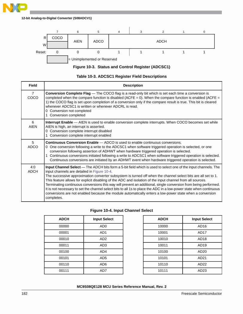
12-bit Analog-to-Digital Converter (S08ADCV1)
7 6 5 4 3 2 1 0
R COCOAIEN ADCO ADCH
W
Reset: 0 0 0 1 1 1 1 1
= Unimplemented or Reserved
Figure 10-3. Status and Control Register (ADCSC1)
Table 10-3. ADCSC1 Register Field Descriptions
Field Description
7COCO
Conversion Complete Flag — The COCO flag is a read-only bit which is set each time a conversion iscompleted when the compare function is disabled (ACFE = 0). When the compare function is enabled (ACFE =1) the COCO flag is set upon completion of a conversion only if the compare result is true. This bit is clearedwhenever ADCSC1 is written or whenever ADCRL is read.0 Conversion not completed1 Conversion completed
6AIEN
Interrupt Enable — AIEN is used to enable conversion complete interrupts. When COCO becomes set whileAIEN is high, an interrupt is asserted.0 Conversion complete interrupt disabled1 Conversion complete interrupt enabled
5ADCO
Continuous Conversion Enable — ADCO is used to enable continuous conversions.0 One conversion following a write to the ADCSC1 when software triggered operation is selected, or one
conversion following assertion of ADHWT when hardware triggered operation is selected.1 Continuous conversions initiated following a write to ADCSC1 when software triggered operation is selected.
Continuous conversions are initiated by an ADHWT event when hardware triggered operation is selected.
4:0ADCH
Input Channel Select — The ADCH bits form a 5-bit field which is used to select one of the input channels. Theinput channels are detailed in Figure 10-4.The successive approximation converter subsystem is turned off when the channel select bits are all set to 1.This feature allows for explicit disabling of the ADC and isolation of the input channel from all sources.Terminating continuous conversions this way will prevent an additional, single conversion from being performed.It is not necessary to set the channel select bits to all 1s to place the ADC in a low-power state when continuousconversions are not enabled because the module automatically enters a low-power state when a conversioncompletes.
Figure 10-4. Input Channel Select
ADCH Input Select ADCH Input Select
00000 AD0 10000 AD16
00001 AD1 10001 AD17
00010 AD2 10010 AD18
00011 AD3 10011 AD19
00100 AD4 10100 AD20
00101 AD5 10101 AD21
00110 AD6 10110 AD22
00111 AD7 10111 AD23
MC9S08QE128 MCU Series Reference Manual, Rev. 2
182 Freescale Semiconductor
12-bit Analog-to-Digital Converter (S08ADCV1)
10.3.2 Status and Control Register 2 (ADCSC2)
The ADCSC2 register is used to control the compare function, conversion trigger and conversion active ofthe ADC module.
Figure 10-5. Status and Control Register 2 (ADCSC2)
01000 AD8 11000 AD24
01001 AD9 11001 AD25
01010 AD10 11010 AD26
01011 AD11 11011 AD27
01100 AD12 11100 Reserved
01101 AD13 11101 VREFH
01110 AD14 11110 VREFL
01111 AD15 11111 Module disabled
7 6 5 4 3 2 1 0
R ADACTADTRG ACFE ACFGT
0 0R1
1 Bits 1 and 0 are reserved bits that must always be written to 0.
R1
W
Reset: 0 0 0 0 0 0 0 0
= Unimplemented or Reserved
Table 10-4. ADCSC2 Register Field Descriptions
Field Description
7ADACT
Conversion Active — ADACT indicates that a conversion is in progress. ADACT is set when a conversion isinitiated and cleared when a conversion is completed or aborted.0 Conversion not in progress1 Conversion in progress
6ADTRG
Conversion Trigger Select — ADTRG is used to select the type of trigger to be used for initiating a conversion.Two types of trigger are selectable: software trigger and hardware trigger. When software trigger is selected, aconversion is initiated following a write to ADCSC1. When hardware trigger is selected, a conversion is initiatedfollowing the assertion of the ADHWT input.0 Software trigger selected1 Hardware trigger selected
Figure 10-4. Input Channel Select (continued)
ADCH Input Select ADCH Input Select
MC9S08QE128 MCU Series Reference Manual, Rev. 2
Freescale Semiconductor 183

12-bit Analog-to-Digital Converter (S08ADCV1)
10.3.3 Data Result High Register (ADCRH)
In 12-bit operation, ADCRH contains the upper four bits of the result of a 12-bit conversion.
In 10-bit mode, ADCRH contains the upper two bits of the result of a 10-bit conversion. When configuredfor 10-bit mode, ADR11 – ADR10 are equal to zero. When configured for 8-bit mode, ADR11 – ADR8are equal to zero.
In both 12-bit and 10-bit mode, ADCRH is updated each time a conversion completes except whenautomatic compare is enabled and the compare condition is not met. In 12-bit and 10-bit mode, readingADCRH prevents the ADC from transferring subsequent conversion results into the result registers untilADCRL is read. If ADCRL is not read until after the next conversion is completed, then the intermediateconversion result is lost. In 8-bit mode there is no interlocking with ADCRL.
In the case that the MODE bits are changed, any data in ADCRH becomes invalid.
10.3.4 Data Result Low Register (ADCRL)
ADCRL contains the lower eight bits of the result of a 12-bit or 10-bit conversion, and all eight bits of an8-bit conversion. This register is updated each time a conversion completes except when automaticcompare is enabled and the compare condition is not met. In 12-bit and 10-bit mode, reading ADCRHprevents the ADC from transferring subsequent conversion results into the result registers until ADCRL isread. If ADCRL is not read until the after next conversion is completed, then the intermediate conversionresults will be lost. In 8-bit mode, there is no interlocking with ADCRH. In the case that the MODE bitsare changed, any data in ADCRL becomes invalid.
5ACFE
Compare Function Enable — ACFE is used to enable the compare function.0 Compare function disabled1 Compare function enabled
4ACFGT
Compare Function Greater Than Enable — ACFGT is used to configure the compare function to trigger whenthe result of the conversion of the input being monitored is greater than or equal to the compare value. Thecompare function defaults to triggering when the result of the compare of the input being monitored is less thanthe compare value.0 Compare triggers when input is less than compare level1 Compare triggers when input is greater than or equal to compare level
7 6 5 4 3 2 1 0
R 0 0 0 0 ADR11 ADR10 ADR9 ADR8
W
Reset: 0 0 0 0 0 0 0 0
= Unimplemented or Reserved
Figure 10-6. Data Result High Register (ADCRH)
Table 10-4. ADCSC2 Register Field Descriptions (continued)
Field Description
MC9S08QE128 MCU Series Reference Manual, Rev. 2
184 Freescale Semiconductor

12-bit Analog-to-Digital Converter (S08ADCV1)
10.3.5 Compare Value High Register (ADCCVH)
In 12-bit mode, the ADCCVH register holds the upper four bits of the 12-bit compare value. These bits arecompared to the upper four bits of the result following a conversion in 12-bit mode when the comparefunction is enabled.
In 10-bit mode, the ADCCVH register holds the upper two bits of the 10-bit compare value (ADCV9 –ADCV8). These bits are compared to the upper two bits of the result following a conversion in 10-bit modewhen the compare function is enabled.
In 8-bit mode, ADCCVH is not used during compare.
10.3.6 Compare Value Low Register (ADCCVL)
This register holds the lower 8 bits of the 12-bit or 10-bit compare value, or all 8 bits of the 8-bit comparevalue. Bits ADCV7:ADCV0 are compared to the lower 8 bits of the result following a conversion in 12-bit,10-bit or 8-bit mode.
10.3.7 Configuration Register (ADCCFG)
ADCCFG is used to select the mode of operation, clock source, clock divide, and configure for low poweror long sample time.
7 6 5 4 3 2 1 0
R ADR7 ADR6 ADR5 ADR4 ADR3 ADR2 ADR1 ADR0
W
Reset: 0 0 0 0 0 0 0 0
= Unimplemented or Reserved
Figure 10-7. Data Result Low Register (ADCRL)
7 6 5 4 3 2 1 0
R 0 0 0 0ADCV11 ADCV10 ADCV9 ADCV8
W
Reset: 0 0 0 0 0 0 0 0
= Unimplemented or Reserved
Figure 10-8. Compare Value High Register (ADCCVH)
7 6 5 4 3 2 1 0
RADCV7 ADCV6 ADCV5 ADCV4 ADCV3 ADCV2 ADCV1 ADCV0
W
Reset: 0 0 0 0 0 0 0 0
Figure 10-9. Compare Value Low Register(ADCCVL)
MC9S08QE128 MCU Series Reference Manual, Rev. 2
Freescale Semiconductor 185
12-bit Analog-to-Digital Converter (S08ADCV1)
7 6 5 4 3 2 1 0
RADLPC ADIV ADLSMP MODE ADICLK
W
Reset: 0 0 0 0 0 0 0 0
Figure 10-10. Configuration Register (ADCCFG)
Table 10-5. ADCCFG Register Field Descriptions
Field Description
7ADLPC
Low Power Configuration — ADLPC controls the speed and power configuration of the successiveapproximation converter. This is used to optimize power consumption when higher sample rates are not required.0 High speed configuration1 Low power configuration: {FC31}The power is reduced at the expense of maximum clock speed.
6:5ADIV
Clock Divide Select — ADIV select the divide ratio used by the ADC to generate the internal clock ADCK.Table 10-6 shows the available clock configurations.
4ADLSMP
Long Sample Time Configuration — ADLSMP selects between long and short sample time. This adjusts thesample period to allow higher impedance inputs to be accurately sampled or to maximize conversion speed forlower impedance inputs. Longer sample times can also be used to lower overall power consumption whencontinuous conversions are enabled if high conversion rates are not required.0 Short sample time1 Long sample time
3:2MODE
Conversion Mode Selection — MODE bits are used to select between 12-, 10- or 8-bit operation. SeeTable 10-7.
1:0ADICLK
Input Clock Select — ADICLK bits select the input clock source to generate the internal clock ADCK. SeeTable 10-8.
Table 10-6. Clock Divide Select
ADIV Divide Ratio Clock Rate
00 1 Input clock
01 2 Input clock ÷ 2
10 4 Input clock ÷ 4
11 8 Input clock ÷ 8
Table 10-7. Conversion Modes
MODE Mode Description
00 8-bit conversion (N=8)
01 12-bit conversion (N=12)
10 10-bit conversion (N=10)
11 Reserved
MC9S08QE128 MCU Series Reference Manual, Rev. 2
186 Freescale Semiconductor

12-bit Analog-to-Digital Converter (S08ADCV1)
10.3.8 Pin Control 1 Register (APCTL1)The pin control registers are used to disable the I/O port control of MCU pins used as analog inputs.APCTL1 is used to control the pins associated with channels 0–7 of the ADC module.
Table 10-8. Input Clock Select
ADICLK Selected Clock Source
00 Bus clock
01 Bus clock divided by 2
10 Alternate clock (ALTCLK)
11 Asynchronous clock (ADACK)
7 6 5 4 3 2 1 0
RADPC7 ADPC6 ADPC5 ADPC4 ADPC3 ADPC2 ADPC1 ADPC0
W
Reset: 0 0 0 0 0 0 0 0
Figure 10-11. Pin Control 1 Register (APCTL1)
Table 10-9. APCTL1 Register Field Descriptions
Field Description
7ADPC7
ADC Pin Control 7 — ADPC7 is used to control the pin associated with channel AD7.0 AD7 pin I/O control enabled1 AD7 pin I/O control disabled
6ADPC6
ADC Pin Control 6 — ADPC6 is used to control the pin associated with channel AD6.0 AD6 pin I/O control enabled1 AD6 pin I/O control disabled
5ADPC5
ADC Pin Control 5 — ADPC5 is used to control the pin associated with channel AD5.0 AD5 pin I/O control enabled1 AD5 pin I/O control disabled
4ADPC4
ADC Pin Control 4 — ADPC4 is used to control the pin associated with channel AD4.0 AD4 pin I/O control enabled1 AD4 pin I/O control disabled
3ADPC3
ADC Pin Control 3 — ADPC3 is used to control the pin associated with channel AD3.0 AD3 pin I/O control enabled1 AD3 pin I/O control disabled
2ADPC2
ADC Pin Control 2 — ADPC2 is used to control the pin associated with channel AD2.0 AD2 pin I/O control enabled1 AD2 pin I/O control disabled
MC9S08QE128 MCU Series Reference Manual, Rev. 2
Freescale Semiconductor 187

12-bit Analog-to-Digital Converter (S08ADCV1)
10.3.9 Pin Control 2 Register (APCTL2)
APCTL2 is used to control channels 8–15 of the ADC module.
1ADPC1
ADC Pin Control 1 — ADPC1 is used to control the pin associated with channel AD1.0 AD1 pin I/O control enabled1 AD1 pin I/O control disabled
0ADPC0
ADC Pin Control 0 — ADPC0 is used to control the pin associated with channel AD0.0 AD0 pin I/O control enabled1 AD0 pin I/O control disabled
7 6 5 4 3 2 1 0
RADPC15 ADPC14 ADPC13 ADPC12 ADPC11 ADPC10 ADPC9 ADPC8
W
Reset: 0 0 0 0 0 0 0 0
Figure 10-12. Pin Control 2 Register (APCTL2)
Table 10-10. APCTL2 Register Field Descriptions
Field Description
7ADPC15
ADC Pin Control 15 — ADPC15 is used to control the pin associated with channel AD15.0 AD15 pin I/O control enabled1 AD15 pin I/O control disabled
6ADPC14
ADC Pin Control 14 — ADPC14 is used to control the pin associated with channel AD14.0 AD14 pin I/O control enabled1 AD14 pin I/O control disabled
5ADPC13
ADC Pin Control 13 — ADPC13 is used to control the pin associated with channel AD13.0 AD13 pin I/O control enabled1 AD13 pin I/O control disabled
4ADPC12
ADC Pin Control 12 — ADPC12 is used to control the pin associated with channel AD12.0 AD12 pin I/O control enabled1 AD12 pin I/O control disabled
3ADPC11
ADC Pin Control 11 — ADPC11 is used to control the pin associated with channel AD11.0 AD11 pin I/O control enabled1 AD11 pin I/O control disabled
2ADPC10
ADC Pin Control 10 — ADPC10 is used to control the pin associated with channel AD10.0 AD10 pin I/O control enabled1 AD10 pin I/O control disabled
Table 10-9. APCTL1 Register Field Descriptions (continued)
Field Description
MC9S08QE128 MCU Series Reference Manual, Rev. 2
188 Freescale Semiconductor

12-bit Analog-to-Digital Converter (S08ADCV1)
10.3.10 Pin Control 3 Register (APCTL3)
APCTL3 is used to control channels 16–23 of the ADC module.
1ADPC9
ADC Pin Control 9 — ADPC9 is used to control the pin associated with channel AD9.0 AD9 pin I/O control enabled1 AD9 pin I/O control disabled
0ADPC8
ADC Pin Control 8 — ADPC8 is used to control the pin associated with channel AD8.0 AD8 pin I/O control enabled1 AD8 pin I/O control disabled
7 6 5 4 3 2 1 0
RADPC23 ADPC22 ADPC21 ADPC20 ADPC19 ADPC18 ADPC17 ADPC16
W
Reset: 0 0 0 0 0 0 0 0
Figure 10-13. Pin Control 3 Register (APCTL3)
Table 10-11. APCTL3 Register Field Descriptions
Field Description
7ADPC23
ADC Pin Control 23 — ADPC23 is used to control the pin associated with channel AD23.0 AD23 pin I/O control enabled1 AD23 pin I/O control disabled
6ADPC22
ADC Pin Control 22 — ADPC22 is used to control the pin associated with channel AD22.0 AD22 pin I/O control enabled1 AD22 pin I/O control disabled
5ADPC21
ADC Pin Control 21 — ADPC21 is used to control the pin associated with channel AD21.0 AD21 pin I/O control enabled1 AD21 pin I/O control disabled
4ADPC20
ADC Pin Control 20 — ADPC20 is used to control the pin associated with channel AD20.0 AD20 pin I/O control enabled1 AD20 pin I/O control disabled
3ADPC19
ADC Pin Control 19 — ADPC19 is used to control the pin associated with channel AD19.0 AD19 pin I/O control enabled1 AD19 pin I/O control disabled
2ADPC18
ADC Pin Control 18 — ADPC18 is used to control the pin associated with channel AD18.0 AD18 pin I/O control enabled1 AD18 pin I/O control disabled
Table 10-10. APCTL2 Register Field Descriptions (continued)
Field Description
MC9S08QE128 MCU Series Reference Manual, Rev. 2
Freescale Semiconductor 189
12-bit Analog-to-Digital Converter (S08ADCV1)
10.4 Functional DescriptionThe ADC module is disabled during reset or when the ADCH bits are all high. The module is idle when aconversion has completed and another conversion has not been initiated. When idle, the module is in itslowest power state.
The ADC can perform an analog-to-digital conversion on any of the software selectable channels. In 12-bitand 10-bit mode, the selected channel voltage is converted by a successive approximation algorithm intoa 12-bit digital result. In 8-bit mode, the selected channel voltage is converted by a successiveapproximation algorithm into a 9-bit digital result.
When the conversion is completed, the result is placed in the data registers (ADCRH and ADCRL). In10-bit mode, the result is rounded to 10 bits and placed in the data registers (ADCRH and ADCRL). In8-bit mode, the result is rounded to 8 bits and placed in ADCRL. The conversion complete flag (COCO)is then set and an interrupt is generated if the conversion complete interrupt has been enabled (AIEN = 1).
The ADC module has the capability of automatically comparing the result of a conversion with thecontents of its compare registers. The compare function is enabled by setting the ACFE bit and operatesin conjunction with any of the conversion modes and configurations.
10.4.1 Clock Select and Divide Control
One of four clock sources can be selected as the clock source for the ADC module. This clock source isthen divided by a configurable value to generate the input clock to the converter (ADCK). The clock isselected from one of the following sources by means of the ADICLK bits.
• The bus clock, which is equal to the frequency at which software is executed. This is the defaultselection following reset.
• The bus clock divided by 2. For higher bus clock rates, this allows a maximum divide by 16 of thebus clock.
• ALTCLK, as defined for this MCU (See module section introduction).
• The asynchronous clock (ADACK) – This clock is generated from a clock source within the ADCmodule. When selected as the clock source this clock remains active while the MCU is in wait orstop3 mode and allows conversions in these modes for lower noise operation.
Whichever clock is selected, its frequency must fall within the specified frequency range for ADCK. If theavailable clocks are too slow, the ADC will not perform according to specifications. If the available clocks
1ADPC17
ADC Pin Control 17 — ADPC17 is used to control the pin associated with channel AD17.0 AD17 pin I/O control enabled1 AD17 pin I/O control disabled
0ADPC16
ADC Pin Control 16 — ADPC16 is used to control the pin associated with channel AD16.0 AD16 pin I/O control enabled1 AD16 pin I/O control disabled
Table 10-11. APCTL3 Register Field Descriptions (continued)
Field Description
MC9S08QE128 MCU Series Reference Manual, Rev. 2
190 Freescale Semiconductor
12-bit Analog-to-Digital Converter (S08ADCV1)
are too fast, then the clock must be divided to the appropriate frequency. This divider is specified by theADIV bits and can be divide-by 1, 2, 4, or 8.
10.4.2 Input Select and Pin Control
The pin control registers (APCTL3, APCTL2, and APCTL1) are used to disable the I/O port control of thepins used as analog inputs.When a pin control register bit is set, the following conditions are forced for theassociated MCU pin:
• The output buffer is forced to its high impedance state.
• The input buffer is disabled. A read of the I/O port returns a zero for any pin with its input bufferdisabled.
• The pullup is disabled.
10.4.3 Hardware Trigger
The ADC module has a selectable asynchronous hardware conversion trigger, ADHWT, that is enabledwhen the ADTRG bit is set. This source is not available on all MCUs. Consult the module introduction forinformation on the ADHWT source specific to this MCU.
When ADHWT source is available and hardware trigger is enabled (ADTRG=1), a conversion is initiatedon the rising edge of ADHWT. If a conversion is in progress when a rising edge occurs, the rising edge isignored. In continuous convert configuration, only the initial rising edge to launch continuous conversionsis observed. The hardware trigger function operates in conjunction with any of the conversion modes andconfigurations.
10.4.4 Conversion Control
Conversions can be performed in 12-bit mode, 10-bit mode or 8-bit mode as determined by the MODEbits. Conversions can be initiated by either a software or hardware trigger. In addition, the ADC modulecan be configured for low power operation, long sample time, continuous conversion, and automaticcompare of the conversion result to a software determined compare value.
10.4.4.1 Initiating Conversions
A conversion is initiated:
• Following a write to ADCSC1 (with ADCH bits not all 1s) if software triggered operation isselected.
• Following a hardware trigger (ADHWT) event if hardware triggered operation is selected.
• Following the transfer of the result to the data registers when continuous conversion is enabled.
If continuous conversions are enabled a new conversion is automatically initiated after the completion ofthe current conversion. In software triggered operation, continuous conversions begin after ADCSC1 iswritten and continue until aborted. In hardware triggered operation, continuous conversions begin after ahardware trigger event and continue until aborted.
MC9S08QE128 MCU Series Reference Manual, Rev. 2
Freescale Semiconductor 191

12-bit Analog-to-Digital Converter (S08ADCV1)
10.4.4.2 Completing Conversions
A conversion is completed when the result of the conversion is transferred into the data result registers,ADCRH and ADCRL. This is indicated by the setting of COCO. An interrupt is generated if AIEN is highat the time that COCO is set.
A blocking mechanism prevents a new result from overwriting previous data in ADCRH and ADCRL ifthe previous data is in the process of being read while in 12-bit or 10-bit MODE (the ADCRH register hasbeen read but the ADCRL register has not). When blocking is active, the data transfer is blocked, COCOis not set, and the new result is lost. In the case of single conversions with the compare function enabledand the compare condition false, blocking has no effect and ADC operation is terminated. In all other casesof operation, when a data transfer is blocked, another conversion is initiated regardless of the state ofADCO (single or continuous conversions enabled).
If single conversions are enabled, the blocking mechanism could result in several discarded conversionsand excess power consumption. To avoid this issue, the data registers must not be read after initiating asingle conversion until the conversion completes.
10.4.4.3 Aborting Conversions
Any conversion in progress will be aborted when:
• A write to ADCSC1 occurs (the current conversion will be aborted and a new conversion will beinitiated, if ADCH are not all 1s).
• A write to ADCSC2, ADCCFG, ADCCVH, or ADCCVL occurs. This indicates a mode ofoperation change has occurred and the current conversion is therefore invalid.
• The MCU is reset.
• The MCU enters stop mode with ADACK not enabled.
When a conversion is aborted, the contents of the data registers, ADCRH and ADCRL, are not altered butcontinue to be the values transferred after the completion of the last successful conversion. In the case thatthe conversion was aborted by a reset, ADCRH and ADCRL return to their reset states.
10.4.4.4 Power Control
The ADC module remains in its idle state until a conversion is initiated. If ADACK is selected as theconversion clock source, the ADACK clock generator is also enabled.
Power consumption when active can be reduced by setting ADLPC. This results in a lower maximum valuefor fADCK (see the electrical specifications).
10.4.4.5 Sample Time and Total Conversion Time
The total conversion time depends on the sample time (as determined by ADLSMP), the MCU busfrequency, the conversion mode (8-bit, 10-bit or 12-bit), and the frequency of the conversion clock (fADCK).After the module becomes active, sampling of the input begins. ADLSMP is used to select between short(3.5 ADCK cycles) and long (23.5 ADCK cycles) sample times.When sampling is complete, the converteris isolated from the input channel and a successive approximation algorithm is performed to determine the
MC9S08QE128 MCU Series Reference Manual, Rev. 2
192 Freescale Semiconductor
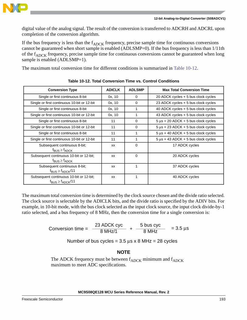
12-bit Analog-to-Digital Converter (S08ADCV1)
digital value of the analog signal. The result of the conversion is transferred to ADCRH and ADCRL uponcompletion of the conversion algorithm.
If the bus frequency is less than the fADCK frequency, precise sample time for continuous conversionscannot be guaranteed when short sample is enabled (ADLSMP=0). If the bus frequency is less than 1/11thof the fADCK frequency, precise sample time for continuous conversions cannot be guaranteed when longsample is enabled (ADLSMP=1).
The maximum total conversion time for different conditions is summarized in Table 10-12.
The maximum total conversion time is determined by the clock source chosen and the divide ratio selected.The clock source is selectable by the ADICLK bits, and the divide ratio is specified by the ADIV bits. Forexample, in 10-bit mode, with the bus clock selected as the input clock source, the input clock divide-by-1ratio selected, and a bus frequency of 8 MHz, then the conversion time for a single conversion is:
NOTEThe ADCK frequency must be between fADCK minimum and fADCKmaximum to meet ADC specifications.
Table 10-12. Total Conversion Time vs. Control Conditions
Conversion Type ADICLK ADLSMP Max Total Conversion Time
Single or first continuous 8-bit 0x, 10 0 20 ADCK cycles + 5 bus clock cycles
Single or first continuous 10-bit or 12-bit 0x, 10 0 23 ADCK cycles + 5 bus clock cycles
Single or first continuous 8-bit 0x, 10 1 40 ADCK cycles + 5 bus clock cycles
Single or first continuous 10-bit or 12-bit 0x, 10 1 43 ADCK cycles + 5 bus clock cycles
Single or first continuous 8-bit 11 0 5 μs + 20 ADCK + 5 bus clock cycles
Single or first continuous 10-bit or 12-bit 11 0 5 μs + 23 ADCK + 5 bus clock cycles
Single or first continuous 8-bit 11 1 5 μs + 40 ADCK + 5 bus clock cycles
Single or first continuous 10-bit or 12-bit 11 1 5 μs + 43 ADCK + 5 bus clock cycles
Subsequent continuous 8-bit;fBUS > fADCK
xx 0 17 ADCK cycles
Subsequent continuous 10-bit or 12-bit;fBUS > fADCK
xx 0 20 ADCK cycles
Subsequent continuous 8-bit;fBUS > fADCK/11
xx 1 37 ADCK cycles
Subsequent continuous 10-bit or 12-bit;fBUS > fADCK/11
xx 1 40 ADCK cycles
23 ADCK cycConversion time = 8 MHz/1
Number of bus cycles = 3.5 μs x 8 MHz = 28 cycles
5 bus cyc8 MHz+ = 3.5 μs
MC9S08QE128 MCU Series Reference Manual, Rev. 2
Freescale Semiconductor 193
12-bit Analog-to-Digital Converter (S08ADCV1)
10.4.5 Automatic Compare Function
The compare function can be configured to check for either an upper limit or lower limit. After the inputis sampled and converted, the result is added to the two’s complement of the compare value (ADCCVHand ADCCVL). When comparing to an upper limit (ACFGT = 1), if the result is greater-than or equal-tothe compare value, COCO is set. When comparing to a lower limit (ACFGT = 0), if the result is less thanthe compare value, COCO is set. The value generated by the addition of the conversion result and the two’scomplement of the compare value is transferred to ADCRH and ADCRL.
Upon completion of a conversion while the compare function is enabled, if the compare condition is nottrue, COCO is not set and no data is transferred to the result registers. An ADC interrupt is generated uponthe setting of COCO if the ADC interrupt is enabled (AIEN = 1).
NOTEThe compare function can be used to monitor the voltage on a channel whilethe MCU is in either wait or stop3 mode. The ADC interrupt will wake theMCU when the compare condition is met.
10.4.6 MCU Wait Mode Operation
The WAIT instruction puts the MCU in a lower power-consumption standby mode from which recoveryis very fast because the clock sources remain active. If a conversion is in progress when the MCU enterswait mode, it continues until completion. Conversions can be initiated while the MCU is in wait mode bymeans of the hardware trigger or if continuous conversions are enabled.
The bus clock, bus clock divided by two, and ADACK are available as conversion clock sources while inwait mode. The use of ALTCLK as the conversion clock source in wait is dependent on the definition ofALTCLK for this MCU. Consult the module introduction for information on ALTCLK specific to thisMCU.
A conversion complete event sets the COCO and generates an ADC interrupt to wake the MCU from waitmode if the ADC interrupt is enabled (AIEN = 1).
10.4.7 MCU Stop3 Mode Operation
The STOP instruction is used to put the MCU in a low power-consumption standby mode during whichmost or all clock sources on the MCU are disabled.
10.4.7.1 Stop3 Mode With ADACK Disabled
If the asynchronous clock, ADACK, is not selected as the conversion clock, executing a STOP instructionaborts the current conversion and places the ADC in its idle state. The contents of ADCRH and ADCRLare unaffected by stop3 mode. After exiting from stop3 mode, a software or hardware trigger is requiredto resume conversions.
MC9S08QE128 MCU Series Reference Manual, Rev. 2
194 Freescale Semiconductor
12-bit Analog-to-Digital Converter (S08ADCV1)
10.4.7.2 Stop3 Mode With ADACK Enabled
If ADACK is selected as the conversion clock, the ADC continues operation during stop3 mode. Forguaranteed ADC operation, the MCU’s voltage regulator must remain active during stop3 mode. Consultthe module introduction for configuration information for this MCU.
If a conversion is in progress when the MCU enters stop3 mode, it continues until completion. Conversionscan be initiated while the MCU is in stop3 mode by means of the hardware trigger or if continuousconversions are enabled.
A conversion complete event sets the COCO and generates an ADC interrupt to wake the MCU from stop3mode if the ADC interrupt is enabled (AIEN = 1).
NOTEIt is possible for the ADC module to wake the system from low power stopand cause the MCU to begin consuming run-level currents withoutgenerating a system level interrupt. To prevent this scenario, softwareshould ensure that the data transfer blocking mechanism (discussed inSection 10.4.4.2, “Completing Conversions) is cleared when entering stop3and continuing ADC conversions.
10.4.8 MCU Stop1 and Stop2 Mode Operation
The ADC module is automatically disabled when the MCU enters either stop1 or stop2 mode. All moduleregisters contain their reset values following exit from stop1 or stop2. Therefore the module must bere-enabled and re-configured following exit from stop1 or stop2.
10.5 Initialization InformationThis section gives an example which provides some basic direction on how a user would initialize andconfigure the ADC module. The user has the flexibility of choosing between configuring the module for8-, 10-, or 12-bit resolution, single or continuous conversion, and a polled or interrupt approach, amongmany other options. Refer to Table 10-6, Table 10-7, and Table 10-8 for information used in this example.
NOTEHexadecimal values designated by a preceding 0x, binary values designatedby a preceding %, and decimal values have no preceding character.
10.5.1 ADC Module Initialization Example
10.5.1.1 Initialization Sequence
Before the ADC module can be used to complete conversions, an initialization procedure must beperformed. A typical sequence is as follows:
1. Update the configuration register (ADCCFG) to select the input clock source and the divide ratioused to generate the internal clock, ADCK. This register is also used for selecting sample time andlow-power configuration.
MC9S08QE128 MCU Series Reference Manual, Rev. 2
Freescale Semiconductor 195

12-bit Analog-to-Digital Converter (S08ADCV1)
2. Update status and control register 2 (ADCSC2) to select the conversion trigger (hardware orsoftware) and compare function options, if enabled.
3. Update status and control register 1 (ADCSC1) to select whether conversions will be continuousor completed only once, and to enable or disable conversion complete interrupts. The input channelon which conversions will be performed is also selected here.
10.5.1.2 Pseudo — Code Example
In this example, the ADC module will be set up with interrupts enabled to perform a single 10-bitconversion at low power with a long sample time on input channel 1, where the internal ADCK clock willbe derived from the bus clock divided by 1.
ADCCFG = 0x98 (%10011000)
Bit 7 ADLPC 1 Configures for low power (lowers maximum clock speed)Bit 6:5 ADIV 00 Sets the ADCK to the input clock ÷ 1Bit 4 ADLSMP 1 Configures for long sample timeBit 3:2 MODE 10 Sets mode at 10-bit conversionsBit 1:0 ADICLK 00 Selects bus clock as input clock source
ADCSC2 = 0x00 (%00000000)
Bit 7 ADACT 0 Flag indicates if a conversion is in progressBit 6 ADTRG 0 Software trigger selectedBit 5 ACFE 0 Compare function disabledBit 4 ACFGT 0 Not used in this exampleBit 3:2 00 Unimplemented or reserved, always reads zeroBit 1:0 00 Reserved for Freescale’s internal use; always write zero
ADCSC1 = 0x41 (%01000001)
Bit 7 COCO 0 Read-only flag which is set when a conversion completesBit 6 AIEN 1 Conversion complete interrupt enabledBit 5 ADCO 0 One conversion only (continuous conversions disabled)Bit 4:0 ADCH 00001 Input channel 1 selected as ADC input channel
ADCRH/L = 0xxx
Holds results of conversion. Read high byte (ADCRH) before low byte (ADCRL) so that conversiondata cannot be overwritten with data from the next conversion.
ADCCVH/L = 0xxx
Holds compare value when compare function enabled
APCTL1=0x02
AD1 pin I/O control disabled. All other AD pins remain general purpose I/O pins
APCTL2=0x00
All other AD pins remain general purpose I/O pins
MC9S08QE128 MCU Series Reference Manual, Rev. 2
196 Freescale Semiconductor

12-bit Analog-to-Digital Converter (S08ADCV1)
Figure 10-14. Initialization Flowchart for Example
10.6 Application InformationThis section contains information for using the ADC module in applications. The ADC has been designedto be integrated into a microcontroller for use in embedded control applications requiring an A/Dconverter.
10.6.1 External Pins and Routing
The following sections discuss the external pins associated with the ADC module and how they should beused for best results.
10.6.1.1 Analog Supply Pins
The ADC module has analog power and ground supplies (VDDAD and VSSAD) which are available asseparate pins on some devices. On other devices, VSSAD is shared on the same pin as the MCU digital VSS,and on others, both VSSAD and VDDAD are shared with the MCU digital supply pins. In these cases, thereare separate pads for the analog supplies which are bonded to the same pin as the corresponding digitalsupply so that some degree of isolation between the supplies is maintained.
When available on a separate pin, both VDDAD and VSSAD must be connected to the same voltage potentialas their corresponding MCU digital supply (VDD and VSS) and must be routed carefully for maximumnoise immunity and bypass capacitors placed as near as possible to the package.
YES
NO
RESET
INITIALIZE ADCADCCFG = $98
ADCSC1 = $41ADCSC2 = $00
CHECKCOCO=1?
READ ADCRHTHEN ADCRL TOCLEAR COCO BIT
CONTINUE
MC9S08QE128 MCU Series Reference Manual, Rev. 2
Freescale Semiconductor 197

12-bit Analog-to-Digital Converter (S08ADCV1)
In cases where separate power supplies are used for analog and digital power, the ground connectionbetween these supplies must be at the VSSAD pin. This should be the only ground connection between thesesupplies if possible. The VSSAD pin makes a good single point ground location.
10.6.1.2 Analog Reference Pins
In addition to the analog supplies, the ADC module has connections for two reference voltage inputs. Thehigh reference is VREFH, which may be shared on the same pin as VDDAD on some devices. The lowreference is VREFL, which may be shared on the same pin as VSSAD on some devices.
When available on a separate pin, VREFH may be connected to the same potential as VDDAD, or may bedriven by an external source that is between the minimum VDDAD spec and the VDDAD potential (VREFHmust never exceed VDDAD). When available on a separate pin, VREFL must be connected to the samevoltage potential as VSSAD. Both VREFH and VREFL must be routed carefully for maximum noiseimmunity and bypass capacitors placed as near as possible to the package.
AC current in the form of current spikes required to supply charge to the capacitor array at each successiveapproximation step is drawn through the VREFH and VREFL loop. The best external component to meet thiscurrent demand is a 0.1 μF capacitor with good high frequency characteristics. This capacitor is connectedbetween VREFH and VREFL and must be placed as near as possible to the package pins. Resistance in thepath is not recommended because the current will cause a voltage drop which could result in conversionerrors. Inductance in this path must be minimum (parasitic only).
10.6.1.3 Analog Input Pins
The external analog inputs are typically shared with digital I/O pins on MCU devices. The pin I/O controlis disabled by setting the appropriate control bit in one of the pin control registers. Conversions can beperformed on inputs without the associated pin control register bit set. It is recommended that the pincontrol register bit always be set when using a pin as an analog input. This avoids problems with contentionbecause the output buffer will be in its high impedance state and the pullup is disabled. Also, the inputbuffer draws DC current when its input is not at either VDD or VSS. Setting the pin control register bits forall pins used as analog inputs should be done to achieve lowest operating current.
Empirical data shows that capacitors on the analog inputs improve performance in the presence of noiseor when the source impedance is high. Use of 0.01 μF capacitors with good high-frequency characteristicsis sufficient. These capacitors are not necessary in all cases, but when used they must be placed as near aspossible to the package pins and be referenced to VSSA.
For proper conversion, the input voltage must fall between VREFH and VREFL. If the input is equal to orexceeds VREFH, the converter circuit converts the signal to $FFF (full scale 12-bit representation), $3FF(full scale 10-bit representation) or $FF (full scale 8-bit representation). If the input is equal to or less thanVREFL, the converter circuit converts it to $000. Input voltages between VREFH and VREFL are straight-linelinear conversions. There will be a brief current associated with VREFL when the sampling capacitor ischarging. The input is sampled for 3.5 cycles of the ADCK source when ADLSMP is low, or 23.5 cycleswhen ADLSMP is high.
For minimal loss of accuracy due to current injection, pins adjacent to the analog input pins should not betransitioning during conversions.
MC9S08QE128 MCU Series Reference Manual, Rev. 2
198 Freescale Semiconductor

12-bit Analog-to-Digital Converter (S08ADCV1)
10.6.2 Sources of Error
Several sources of error exist for A/D conversions. These are discussed in the following sections.
10.6.2.1 Sampling Error
For proper conversions, the input must be sampled long enough to achieve the proper accuracy. Given themaximum input resistance of approximately 7kΩ and input capacitance of approximately 5.5 pF, samplingto within 1/4LSB (at 12-bit resolution) can be achieved within the minimum sample window (3.5 cycles @8 MHz maximum ADCK frequency) provided the resistance of the external analog source (RAS) is keptbelow 2 kΩ.
Higher source resistances or higher-accuracy sampling is possible by setting ADLSMP (to increase thesample window to 23.5 cycles) or decreasing ADCK frequency to increase sample time.
10.6.2.2 Pin Leakage Error
Leakage on the I/O pins can cause conversion error if the external analog source resistance (RAS) is high.If this error cannot be tolerated by the application, keep RAS lower than VDDAD / (2N*ILEAK) for less than1/4LSB leakage error (N = 8 in 8-bit, 10 in 10-bit or 12 in 12-bit mode).
10.6.2.3 Noise-Induced Errors
System noise which occurs during the sample or conversion process can affect the accuracy of theconversion. The ADC accuracy numbers are guaranteed as specified only if the following conditions aremet:
• There is a 0.1 μF low-ESR capacitor from VREFH to VREFL.
• There is a 0.1 μF low-ESR capacitor from VDDAD to VSSAD.
• If inductive isolation is used from the primary supply, an additional 1 μF capacitor is placed fromVDDAD to VSSAD.
• VSSAD (and VREFL, if connected) is connected to VSS at a quiet point in the ground plane.
• Operate the MCU in wait or stop3 mode before initiating (hardware triggered conversions) orimmediately after initiating (hardware or software triggered conversions) the ADC conversion.
— For software triggered conversions, immediately follow the write to the ADCSC1 with a WAITinstruction or STOP instruction.
— For stop3 mode operation, select ADACK as the clock source. Operation in stop3 reduces VDDnoise but increases effective conversion time due to stop recovery.
• There is no I/O switching, input or output, on the MCU during the conversion.
There are some situations where external system activity causes radiated or conducted noise emissions orexcessive VDD noise is coupled into the ADC. In these situations, or when the MCU cannot be placed inwait or stop3 or I/O activity cannot be halted, these recommended actions may reduce the effect of noiseon the accuracy:
• Place a 0.01 μF capacitor (CAS) on the selected input channel to VREFL or VSSAD (this willimprove noise issues but will affect sample rate based on the external analog source resistance).
MC9S08QE128 MCU Series Reference Manual, Rev. 2
Freescale Semiconductor 199

12-bit Analog-to-Digital Converter (S08ADCV1)
• Average the result by converting the analog input many times in succession and dividing the sumof the results. Four samples are required to eliminate the effect of a 1LSB, one-time error.
• Reduce the effect of synchronous noise by operating off the asynchronous clock (ADACK) andaveraging. Noise that is synchronous to ADCK cannot be averaged out.
10.6.2.4 Code Width and Quantization Error
The ADC quantizes the ideal straight-line transfer function into 4096 steps (in 12-bit mode). Each stepideally has the same height (1 code) and width. The width is defined as the delta between the transitionpoints to one code and the next. The ideal code width for an N bit converter (in this case N can be 8, 10 or12), defined as 1LSB, is:
1LSB = (VREFH - VREFL) / 2N Eqn. 10-2
There is an inherent quantization error due to the digitization of the result. For 8-bit or 10-bit conversionsthe code will transition when the voltage is at the midpoint between the points where the straight linetransfer function is exactly represented by the actual transfer function. Therefore, the quantization errorwill be ± 1/2LSB in 8- or 10-bit mode. As a consequence, however, the code width of the first ($000)conversion is only 1/2LSB and the code width of the last ($FF or $3FF) is 1.5LSB.
For 12-bit conversions the code transitions only after the full code width is present, so the quantizationerror is -1LSB to 0LSB and the code width of each step is 1LSB.
10.6.2.5 Linearity Errors
The ADC may also exhibit non-linearity of several forms. Every effort has been made to reduce theseerrors but the system should be aware of them because they affect overall accuracy. These errors are:
• Zero-scale error (EZS) (sometimes called offset) — This error is defined as the difference betweenthe actual code width of the first conversion and the ideal code width (1/2LSB in 8-bit or 10-bitmodes and 1LSB in 12-bit mode). Note, if the first conversion is $001, then the difference betweenthe actual $001 code width and its ideal (1LSB) is used.
• Full-scale error (EFS) — This error is defined as the difference between the actual code width ofthe last conversion and the ideal code width (1.5LSB in 8-bit or 10-bit modes and 1LSB in 12-bitmode). Note, if the last conversion is $3FE, then the difference between the actual $3FE code widthand its ideal (1LSB) is used.
• Differential non-linearity (DNL) — This error is defined as the worst-case difference between theactual code width and the ideal code width for all conversions.
• Integral non-linearity (INL) — This error is defined as the highest-value the (absolute value of the)running sum of DNL achieves. More simply, this is the worst-case difference of the actualtransition voltage to a given code and its corresponding ideal transition voltage, for all codes.
• Total unadjusted error (TUE) — This error is defined as the difference between the actual transferfunction and the ideal straight-line transfer function, and therefore includes all forms of error.
MC9S08QE128 MCU Series Reference Manual, Rev. 2
200 Freescale Semiconductor

12-bit Analog-to-Digital Converter (S08ADCV1)
10.6.2.6 Code Jitter, Non-Monotonicity and Missing Codes
Analog-to-digital converters are susceptible to three special forms of error. These are code jitter,non-monotonicity, and missing codes.
Code jitter is when, at certain points, a given input voltage converts to one of two values when sampledrepeatedly. Ideally, when the input voltage is infinitesimally smaller than the transition voltage, theconverter yields the lower code (and vice-versa). However, even very small amounts of system noise cancause the converter to be indeterminate (between two codes) for a range of input voltages around thetransition voltage. This range is normally around 1/2LSB in 8-bit or 10-bit mode, or around 2 LSB in 12-bitmode, and will increase with noise.
This error may be reduced by repeatedly sampling the input and averaging the result. Additionally thetechniques discussed in Section 10.6.2.3 will reduce this error.
Non-monotonicity is defined as when, except for code jitter, the converter converts to a lower code for ahigher input voltage. Missing codes are those values which are never converted for any input value.
In 8-bit or 10-bit mode, the ADC is guaranteed to be monotonic and to have no missing codes.
MC9S08QE128 MCU Series Reference Manual, Rev. 2
Freescale Semiconductor 201

12-bit Analog-to-Digital Converter (S08ADCV1)
MC9S08QE128 MCU Series Reference Manual, Rev. 2
202 Freescale Semiconductor

Chapter 11Internal Clock Source (S08ICSV3)
11.1 IntroductionThe internal clock source (ICS) module provides clock source choices for the MCU. The module containsa frequency-locked loop (FLL) as a clock source that is controllable by either an internal or an externalreference clock. The module can provide this FLL clock or either of the internal or external referenceclocks as a source for the MCU system clock.
The ICSTRM and FTRIM bits are normally reset to the factory trim values on any reset. However, anyreset that puts the device into BDM (a POR with the BKGD pin held low or a development tool settingSBDFR[BDFR]) results in the ICSTRM and FTRIM bits being set to values of 0x80 and 0. Whendebugging the MCU, the factory trim value can be used by copying the trim values from the Flash locationsshown in table 4-4.
There are also signals provided to control a low power oscillator (XOSCVLP) module to allow the use ofan external crystal/resonator as the external reference clock.
Whichever clock source is chosen, it is passed through a reduced bus divider (BDIV) which allows a lowerfinal output clock frequency to be derived.
11.1.1 External Oscillator
The external oscillator module (XOSCVLP) provides the external clock opitons to the ICS module. Theoutput of this submodule (OSCOUT) can be used as the real-time counter module (RTC) clock source.
11.1.2 Stop2 Mode Considerations
If you are using a low range oscillator during stop2, reconfigure the ICSC2 register (the oscillator controlbits) before PPDACK is written. The low range (RANGE=0) oscillator can operate in stop2 to be the clocksource for the RTC module. If the low range oscillator is active when entering stop2, it remains active instop2 regardless of the value of EREFSTEN. To disable the oscillator in stop2, switch the ICS into FBI orFEI mode before executing the STOP instruction.
Figure 11-1 shows the MC9S08QE128 Series block diagram with the ICS highlighted.
MC9S08QE128 MCU Series Reference Manual, Rev. 2
Freescale Semiconductor 203
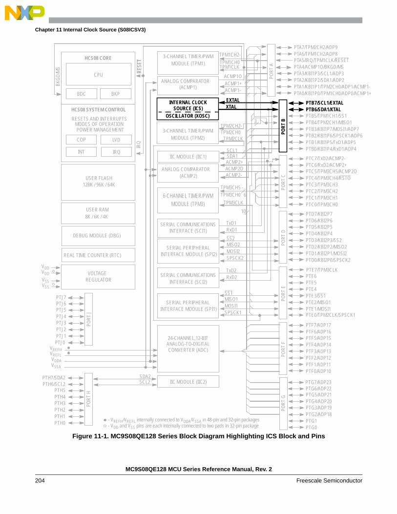
Chapter 11 Internal Clock Source (S08ICSV3)
-+
Figure 11-1. MC9S08QE128 Series Block Diagram Highlighting ICS Block and Pins
TPM2CH2-TPM2CH0
TPM1CH0
TPM1CH2-
ANALOG COMPARATOR(ACMP1)
ACMP1O
ACMP1-ACMP1+
VSS
VDD
IIC MODULE (IIC1)
SERIAL PERIPHERAL INTERFACE MODULE (SPI1)
USER FLASH
USER RAM
128K / 96K / 64K
HCS08 CORE
CPU
BDC
6-CHANNEL TIMER/PWMMODULE (TPM3)
HCS08 SYSTEM CONTROL
RESETS AND INTERRUPTSMODES OF OPERATIONPOWER MANAGEMENT
VOLTAGEREGULATOR
COP
IRQ
LVDR
ESET
VREFL
VREFH
8K / 6K / 4K
BKG
D/M
S
INTERFACE (SCI1)SERIAL COMMUNICATIONS
MISO1SS1
SPSCK1
3-CHANNEL TIMER/PWMMODULE (TPM2)
REAL TIME COUNTER (RTC)
DEBUG MODULE (DBG)
IRQ
PTA3/KBI1P3/SCL1/ADP3PTA4/ACMP1O/BKGD/MSPTA5/IRQ/TPM1CLK/RESET
PTA2/KBI1P2/SDA1/ADP2PTA1/KBI1P1/TPM2CH0/ADP1/ACMP1PTA0/KBI1P0/TPM1CH0/ADP0/ACMP1
PORT
A
PTA6/TPM1CH2/ADP8PTA7/TPM2CH2/ADP9
MOSI1
PTB3/KBI1P7/MOSI1/ADP7PTB4/TPM2CH1/MISO1PTB5/TPM1CH1/SS1
PTB2/KBI1P6/SPSCK1/ADP6PTB1/KBI1P5/TxD1/ADP5PTB0/KBI1P4/RxD1/ADP4
PTC3/TPM3CH3PTC4/TPM3CH4/RSTOPTC5/TPM3CH5/ACMP2O
PTC2/TPM3CH2PTC1/TPM3CH1PTC0/TPM3CH0
PORT
C
PTC6/RxD2/ACMP2+PTC7/TxD2/ACMP2-
PTD3/KBI2P3/SS2PTD4/KBI2P4PTD5/KBI2P5
PTD2/KBI2P2/MISO2PTD1/KBI2P1/MOSI2PTD0/KBI2P0/SPSCK2
PORT
D
PTD6/KBI2P6PTD7/KBI2P7
PTE3/SS1PTE4PTE5
PTE2/MISO1PTE1/MOSI1
TPM2CLK
PORT
EPTE6
PTE0/TPM2CLK/SPSCK1
PTF3/ADP13PTF4/ADP14PTF5/ADP15
PTF2/ADP12PTF1/ADP11PTF0/ADP10
PORT
F
PTF6/ADP16PTF7/ADP17
PTG1PTG2/ADP18PTG3/ADP19PO
RT G
PTG4/ADP20PTG5/ADP21
PTG0
VSS
VDD
VSSA
VDDA
BKP
INT
ANALOG COMPARATOR(ACMP2)
INTERFACE (SCI2)SERIAL COMMUNICATIONS
6TPM3CH5 -TPM3CH0
- VREFH/VREFL internally connected to VDDA/VSSA in 48-pin and 32-pin packages- VDD and VSS pins are each internally connected to two pads in 32-pin package
PTG6/ADP22PTG7/ADP23
RES
ET
PORT
JPO
RT H
PTJ1PTJ2PTJ3PTJ4PTJ5
PTJ0
PTJ6PTJ7
PTH1PTH2PTH3PTH4PTH5
PTH0
PTH6/SCL2PTH7/SDA2
IIC MODULE (IIC2)
ANALOG-TO-DIGITALCONVERTER (ADC)
24-CHANNEL,12-BIT
3-CHANNEL TIMER/PWMMODULE (TPM1)
SDA2SCL2
SERIAL PERIPHERAL INTERFACE MODULE (SPI2)
MISO2SS2
SPSCK2MOSI2
10
SDA1SCL1
ACMP2-
ACMP2+ACMP2O
RxD1TxD1
RxD2TxD2
TPM3CLK
3
TPM1CLK
PTE7/TPM3CLK
OSCILLATOR (XOSC)
PORT
B
PTB6/SDA1/XTALPTB7/SCL1/EXTAL
SOURCE (ICS)INTERNAL CLOCK EXTAL
XTAL
MC9S08QE128 MCU Series Reference Manual, Rev. 2
204 Freescale Semiconductor

Internal Clock Source (S08ICSV3)
11.1.3 Features
Key features of the ICS module are:
• Frequency-locked loop (FLL) is trimmable for accuracy
• Internal or external reference clocks can be used to control the FLL
• Reference divider is provided for external clock
• Internal reference clock has 9 trim bits available
• Internal or external reference clocks can be selected as the clock source for the MCU
• Whichever clock is selected as the source can be divided down
— 2 bit select for clock divider is provided
– Allowable dividers are: 1, 2, 4, 8
• Control signals for a low power oscillator as the external reference clock are provided
— HGO, RANGE, EREFS, ERCLKEN, EREFSTEN
• FLL Engaged Internal mode is automatically selected out of reset
• BDC clock is provided as a constant divide by 2 of the low range DCO output
• Three selectable digitally controlled oscillators (DCO) optimized for different frequency ranges.
• Option to maximize output frequency for a 32768 Hz external reference clock source.
11.1.4 Block Diagram
Figure 11-2 is the ICS block diagram.
MC9S08QE128 MCU Series Reference Manual, Rev. 2
Freescale Semiconductor 205

Internal Clock Source (S08ICSV3)
Figure 11-2. Internal Clock Source (ICS) Block Diagram
11.1.5 Modes of Operation
There are seven modes of operation for the ICS: FEI, FEE, FBI, FBILP, FBE, FBELP, and stop.
11.1.5.1 FLL Engaged Internal (FEI)
In FLL engaged internal mode, which is the default mode, the ICS supplies a clock derived from the FLLwhich is controlled by the internal reference clock. The BDC clock is supplied from the FLL.
11.1.5.2 FLL Engaged External (FEE)
In FLL engaged external mode, the ICS supplies a clock derived from the FLL which is controlled by anexternal reference clock. The BDC clock is supplied from the FLL.
11.1.5.3 FLL Bypassed Internal (FBI)
In FLL bypassed internal mode, the FLL is enabled and controlled by the internal reference clock, but isbypassed. The ICS supplies a clock derived from the internal reference clock. The BDC clock is suppliedfrom the FLL.
RDIVTRIM
/ 2
External Reference
IREFS
Clock
CLKS
n=0-10
/ 2n
n=0-3
/ 2nInternal
ReferenceClock
BDIV
ICSLCLK
ICSOUT
ICSIRCLK
EREFS
RANGE
EREFSTENHGO
IREFSTEN
ICSERCLK
Internal Clock Source BlockICSFFCLK
ERCLKEN
IRCLKEN
DCOOUT
DCOLDCOMDCOH
Filter
DRS
LP
FLL
DMX32FTRIM
DRST IREFST CLKST OSCINIT
ICSDCLK
MC9S08QE128 MCU Series Reference Manual, Rev. 1.11
206 Freescale Semiconductor

Internal Clock Source (S08ICSV3)
11.1.5.4 FLL Bypassed Internal Low Power (FBILP)
In FLL bypassed internal low power mode, the FLL is disabled and bypassed, and the ICS supplies a clockderived from the internal reference clock. The BDC clock is not available.
11.1.5.5 FLL Bypassed External (FBE)
In FLL bypassed external mode, the FLL is enabled and controlled by an external reference clock, but isbypassed. The ICS supplies a clock derived from the external reference clock. The external reference clockcan be an external crystal/resonator supplied by an OSC controlled by the ICS, or it can be another externalclock source. The BDC clock is supplied from the FLL.
11.1.5.6 FLL Bypassed External Low Power (FBELP)
In FLL bypassed external low power mode, the FLL is disabled and bypassed, and the ICS supplies a clockderived from the external reference clock. The external reference clock can be an external crystal/resonatorsupplied by an OSC controlled by the ICS, or it can be another external clock source. The BDC clock isnot available.
11.1.5.7 Stop (STOP)
In stop mode the FLL is disabled and the internal or external reference clocks can be selected to be enabledor disabled. The BDC clock is not available and the ICS does not provide an MCU clock source.
11.2 External Signal DescriptionThere are no ICS signals that connect off chip.
11.3 Register DefinitionFigure 11-1 is a summary of ICS registers.
Table 11-1. ICS Register Summary
Name 7 6 5 4 3 2 1 0
ICSC1R
CLKS RDIV IREFS IRCLKEN IREFSTENW
ICSC2R
BDIV RANGE HGO LP EREFS ERCLKEN EREFSTENW
ICSTRMR
TRIMW
ICSSCR DRST
DMX32IREFST CLKST OSCINIT
FTRIMW DRS
MC9S08QE128 MCU Series Reference Manual, Rev. 2
Freescale Semiconductor 207

Internal Clock Source (S08ICSV3)
11.3.1 ICS Control Register 1 (ICSC1)
7 6 5 4 3 2 1 0
RCLKS RDIV IREFS IRCLKEN IREFSTEN
W
Reset: 0 0 0 0 0 1 0 0
Figure 11-3. ICS Control Register 1 (ICSC1)
Table 11-2. ICS Control Register 1 Field Descriptions
Field Description
7:6CLKS
Clock Source Select — Selects the clock source that controls the bus frequency. The actual bus frequencydepends on the value of the BDIV bits.00 Output of FLL is selected.01 Internal reference clock is selected.10 External reference clock is selected.11 Reserved, defaults to 00.
5:3RDIV
Reference Divider — Selects the amount to divide down the external reference clock. Resulting frequency mustbe in the range 31.25 kHz to 39.0625 kHz. See Table 11-3 for the divide-by factors.
2IREFS
Internal Reference Select — The IREFS bit selects the reference clock source for the FLL.1 Internal reference clock selected0 External reference clock selected
1IRCLKEN
Internal Reference Clock Enable — The IRCLKEN bit enables the internal reference clock for use asICSIRCLK.1 ICSIRCLK active0 ICSIRCLK inactive
0IREFSTEN
Internal Reference Stop Enable — The IREFSTEN bit controls whether or not the internal reference clockremains enabled when the ICS enters stop mode.1 Internal reference clock stays enabled in stop if IRCLKEN is set before entering stop0 Internal reference clock is disabled in stop
Table 11-3. Reference Divide Factor
RDIV RANGE=0 RANGE=1
0 11
1 Reset default
32
1 2 64
2 4 128
3 8 256
4 16 512
5 32 1024
6 64 Reserved
7 128 Reserved
MC9S08QE128 MCU Series Reference Manual, Rev. 1.11
208 Freescale Semiconductor
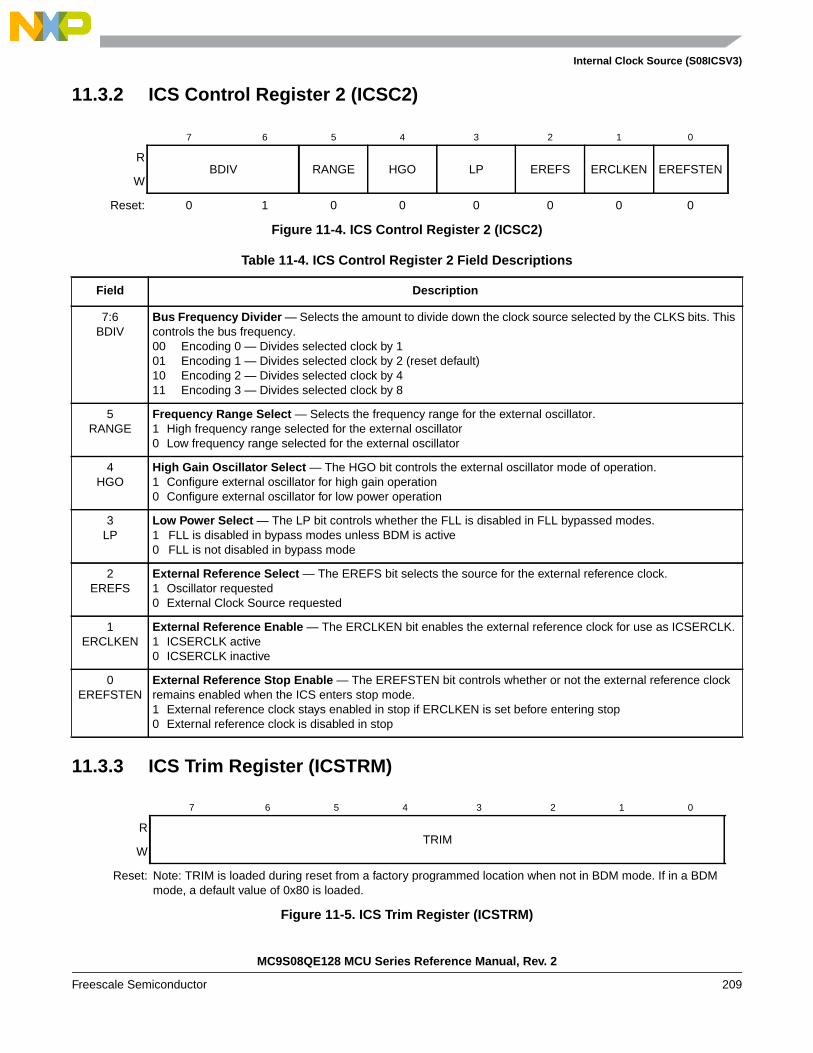
Internal Clock Source (S08ICSV3)
11.3.2 ICS Control Register 2 (ICSC2)
11.3.3 ICS Trim Register (ICSTRM)
7 6 5 4 3 2 1 0
RBDIV RANGE HGO LP EREFS ERCLKEN EREFSTEN
W
Reset: 0 1 0 0 0 0 0 0
Figure 11-4. ICS Control Register 2 (ICSC2)
Table 11-4. ICS Control Register 2 Field Descriptions
Field Description
7:6BDIV
Bus Frequency Divider — Selects the amount to divide down the clock source selected by the CLKS bits. Thiscontrols the bus frequency.00 Encoding 0 — Divides selected clock by 101 Encoding 1 — Divides selected clock by 2 (reset default)10 Encoding 2 — Divides selected clock by 411 Encoding 3 — Divides selected clock by 8
5RANGE
Frequency Range Select — Selects the frequency range for the external oscillator.1 High frequency range selected for the external oscillator0 Low frequency range selected for the external oscillator
4HGO
High Gain Oscillator Select — The HGO bit controls the external oscillator mode of operation.1 Configure external oscillator for high gain operation0 Configure external oscillator for low power operation
3LP
Low Power Select — The LP bit controls whether the FLL is disabled in FLL bypassed modes.1 FLL is disabled in bypass modes unless BDM is active0 FLL is not disabled in bypass mode
2EREFS
External Reference Select — The EREFS bit selects the source for the external reference clock.1 Oscillator requested0 External Clock Source requested
1ERCLKEN
External Reference Enable — The ERCLKEN bit enables the external reference clock for use as ICSERCLK.1 ICSERCLK active0 ICSERCLK inactive
0EREFSTEN
External Reference Stop Enable — The EREFSTEN bit controls whether or not the external reference clockremains enabled when the ICS enters stop mode.1 External reference clock stays enabled in stop if ERCLKEN is set before entering stop0 External reference clock is disabled in stop
7 6 5 4 3 2 1 0
RTRIM
W
Reset: Note: TRIM is loaded during reset from a factory programmed location when not in BDM mode. If in a BDMmode, a default value of 0x80 is loaded.
Figure 11-5. ICS Trim Register (ICSTRM)
MC9S08QE128 MCU Series Reference Manual, Rev. 2
Freescale Semiconductor 209

Internal Clock Source (S08ICSV3)
11.3.4 ICS Status and Control (ICSSC)
Table 11-5. ICS Trim Register Field Descriptions
Field Description
7:0TRIM
ICS Trim Setting — The TRIM bits control the internal reference clock frequency by controlling the internalreference clock period. The bits’ effect are binary weighted (i.e., bit 1 will adjust twice as much as bit 0).Increasing the binary value in TRIM will increase the period, and decreasing the value will decrease the period.
An additional fine trim bit is available in ICSSC as the FTRIM bit.
7 6 5 4 3 2 1 0
R DRSTDMX32
IREFST CLKST OSCINITFTRIM1
1 FTRIM is loaded during reset from a factory programmed location when not in any BDM mode. If in a BDM mode, FTRIMgets loaded with a value of 1’b0.
W DRS
Reset: 0 0 0 1 0 0 0
Figure 11-6. ICS Status and Control Register (ICSSC)
Table 11-6. ICS Status and Control Register Field Descriptions
Field Description
7-6DRSTDRS
DCO Range Status — The DRST read field indicates the current frequency range for the FLL output, DCOOUT.See Table 11-7. The DRST field does not update immediately after a write to the DRS field due to internalsynchronization between clock domains. Writing the DRS bits to 2’b11 will be ignored and the DRST bits willremain with the current setting.
DCO Range Select — The DRS field selects the frequency range for the FLL output, DCOOUT. Writes to theDRS field while the LP bit is set are ignored.00 Low range.01 Mid range.10 High range.11 Reserved.
5DMX32
DCO Maximum frequency with 32.768 kHz reference — The DMX32 bit controls whether or not the DCOfrequency range is narrowed to its maximum frequency with a 32.768 kHz reference. See Table 11-7.0 DCO has default range of 25%.1 DCO is fined tuned for maximum frequency with 32.768 kHz reference.
4IREFST
Internal Reference Status — The IREFST bit indicates the current source for the reference clock. The IREFSTbit does not update immediately after a write to the IREFS bit due to internal synchronization between clockdomains.0 Source of reference clock is external clock.1 Source of reference clock is internal clock.
MC9S08QE128 MCU Series Reference Manual, Rev. 1.11
210 Freescale Semiconductor

Internal Clock Source (S08ICSV3)
r
3-2CLKST
Clock Mode Status — The CLKST bits indicate the current clock mode. The CLKST bits don’t updateimmediately after a write to the CLKS bits due to internal synchronization between clock domains.00 Output of FLL is selected.01 FLL Bypassed, Internal reference clock is selected.10 FLL Bypassed, External reference clock is selected.11 Reserved.
1OSCINIT
OSC Initialization — If the external reference clock is selected by ERCLKEN or by the ICS being in FEE, FBE,or FBELP mode, and if EREFS is set, then this bit is set after the initialization cycles of the external oscillatorclock have completed. This bit is only cleared when either ERCLKEN or EREFS are cleared.
0FTRIM
ICS Fine Trim — The FTRIM bit controls the smallest adjustment of the internal reference clock frequency.Setting FTRIM will increase the period and clearing FTRIM will decrease the period by the smallest amountpossible.
Table 11-7. DCO frequency range1
1 The resulting bus clock frequency should not exceed the maximum specified busclock frequency of the device.
DRS DMX32 Reference range FLL factor DCO range
000 31.25 - 39.0625 kHz 512 16 - 20 Mhz
1 32.768 kHz 608 19.92 Mhz
010 31.25 - 39.0625 kHz 1024 32 - 40 Mhz
1 32.768 kHz 1216 39.85 Mhz
100 31.25 - 39.0625 kHz 1536 48 - 60 Mhz
1 32.768 kHz 1824 59.77 Mhz
11 Reserved
Table 11-6. ICS Status and Control Register Field Descriptions (continued)
Field Description
MC9S08QE128 MCU Series Reference Manual, Rev. 2
Freescale Semiconductor 211
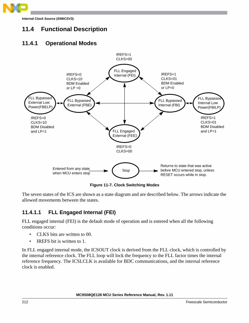
Internal Clock Source (S08ICSV3)
11.4 Functional Description
11.4.1 Operational Modes
Figure 11-7. Clock Switching Modes
The seven states of the ICS are shown as a state diagram and are described below. The arrows indicate theallowed movements between the states.
11.4.1.1 FLL Engaged Internal (FEI)
FLL engaged internal (FEI) is the default mode of operation and is entered when all the followingconditions occur:
• CLKS bits are written to 00.
• IREFS bit is written to 1.
In FLL engaged internal mode, the ICSOUT clock is derived from the FLL clock, which is controlled bythe internal reference clock. The FLL loop will lock the frequency to the FLL factor times the internalreference frequency. The ICSLCLK is available for BDC communications, and the internal referenceclock is enabled.
FLL BypassedInternal LowPower(FBILP)
IREFS=1CLKS=00
Entered from any statewhen MCU enters stop
FLL EngagedInternal (FEI)
FLL BypassedInternal (FBI)
FLL BypassedExternal (FBE)
FLL EngagedExternal (FEE)
FLL BypassedExternal LowPower(FBELP)
IREFS=0CLKS=00
IREFS=0CLKS=10BDM Enabledor LP =0
Returns to state that was activebefore MCU entered stop, unlessRESET occurs while in stop.
IREFS=0CLKS=10BDM Disabledand LP=1
IREFS=1CLKS=01BDM Enabledor LP=0
IREFS=1CLKS=01BDM Disabledand LP=1
Stop
MC9S08QE128 MCU Series Reference Manual, Rev. 1.11
212 Freescale Semiconductor
Internal Clock Source (S08ICSV3)
11.4.1.2 FLL Engaged External (FEE)
The FLL engaged external (FEE) mode is entered when all the following conditions occur:
• CLKS bits are written to 00.
• IREFS bit is written to 0.
• RDIV bits are written to divide external reference clock to be within the range of 31.25 kHz to39.0625 kHz.
In FLL engaged external mode, the ICSOUT clock is derived from the FLL clock which is controlled bythe external reference clock.The FLL loop will lock the frequency to the FLL factor times the externalreference frequency, as selected by the RDIV bits. The ICSLCLK is available for BDC communications,and the external reference clock is enabled.
11.4.1.3 FLL Bypassed Internal (FBI)
The FLL bypassed internal (FBI) mode is entered when all the following conditions occur:
• CLKS bits are written to 01.
• IREFS bit is written to 1.
• BDM mode is active or LP bit is written to 0.
In FLL bypassed internal mode, the ICSOUT clock is derived from the internal reference clock. The FLLclock is controlled by the internal reference clock, and the FLL loop will lock the FLL frequency to theFLL factor times the internal reference frequency. The ICSLCLK will be available for BDCcommunications, and the internal reference clock is enabled.
11.4.1.4 FLL Bypassed Internal Low Power (FBILP)
The FLL bypassed internal low power (FBILP) mode is entered when all the following conditions occur:
• CLKS bits are written to 01
• IREFS bit is written to 1.
• BDM mode is not active and LP bit is written to 1
In FLL bypassed internal low power mode, the ICSOUT clock is derived from the internal reference clockand the FLL is disabled. The ICSLCLK will be not be available for BDC communications, and the internalreference clock is enabled.
11.4.1.5 FLL Bypassed External (FBE)
The FLL bypassed external (FBE) mode is entered when all the following conditions occur:
• CLKS bits are written to 10.
• IREFS bit is written to 0.
• RDIV bits are written to divide external reference clock to be within the range of 31.25 kHz to39.0625 kHz.
• BDM mode is active or LP bit is written to 0.
MC9S08QE128 MCU Series Reference Manual, Rev. 2
Freescale Semiconductor 213

Internal Clock Source (S08ICSV3)
In FLL bypassed external mode, the ICSOUT clock is derived from the external reference clock. The FLLclock is controlled by the external reference clock, and the FLL loop will lock the FLL frequency to theFLL factor times the external reference frequency, as selected by the RDIV bits, so that the ICSLCLK willbe available for BDC communications, and the external reference clock is enabled.
11.4.1.6 FLL Bypassed External Low Power (FBELP)
The FLL bypassed external low power (FBELP) mode is entered when all the following conditions occur:
• CLKS bits are written to 10.
• IREFS bit is written to 0.
• BDM mode is not active and LP bit is written to 1.
In FLL bypassed external low power mode, the ICSOUT clock is derived from the external reference clockand the FLL is disabled. The ICSLCLK will be not be available for BDC communications. The externalreference clock is enabled.
11.4.1.7 Stop
Stop mode is entered whenever the MCU enters a STOP state. In this mode, all ICS clock signals are staticexcept in the following cases:
ICSIRCLK will be active in stop mode when all the following conditions occur:
• IRCLKEN bit is written to 1
• IREFSTEN bit is written to 1
ICSERCLK will be active in stop mode when all the following conditions occur:
• ERCLKEN bit is written to 1EREFSTEN bit is written to 1
•
11.4.2 Mode Switching
The IREF bit can be changed at anytime, but the actual switch to the newly selected clock is shown by theIREFST bit. When switching between FLL engaged internal (FEI) and FLL engaged external (FEE)modes, the FLL will begin locking again after the switch is completed.
The CLKS bits can also be changed at anytime, but the actual switch to the newly selected clock is shownby the CLKST bits. If the newly selected clock is not available, the previous clock will remain selected.
The DRS bits can be changed at anytime except when LP bit is 1. If the DRS bits are changed while inFLL engaged internal (FEI) or FLL engaged external (FEE), the bus clock remains at the previous DCOrange until the new DCO starts. When the new DCO starts the bus clock switches to it. After switching tothe new DCO the FLL remains unlocked for several reference cycles. Once the selected DCO startup timeis over, the FLL is locked. The completion of the switch is shown by the DRST bits.
MC9S08QE128 MCU Series Reference Manual, Rev. 1.11
214 Freescale Semiconductor
Internal Clock Source (S08ICSV3)
11.4.3 Bus Frequency Divider
The BDIV bits can be changed at anytime and the actual switch to the new frequency will occurimmediately.
11.4.4 Low Power Bit Usage
The low power bit (LP) is provided to allow the FLL to be disabled and thus conserve power when it is notbeing used. The DRS bits can not be written while LP bit is 1.
However, in some applications it may be desirable to allow the FLL to be enabled and to lock for maximumaccuracy before switching to an FLL engaged mode. Do this by writing the LP bit to 0.
11.4.5 DCO Maximum Frequency with 32.768 kHz Oscillator
The FLL has an option to change the clock multiplier for the selected DCO range such that it results in themaximum bus frequency with a common 32.768 kHZ crystal reference clock.
11.4.6 Internal Reference Clock
When IRCLKEN is set the internal reference clock signal will be presented as ICSIRCLK, which can beused as an additional clock source. The ICSIRCLK frequency can be re-targeted by trimming the periodof the internal reference clock. This can be done by writing a new value to the TRIM bits in the ICSTRMregister. Writing a larger value will slow down the ICSIRCLK frequency, and writing a smaller value tothe ICSTRM register will speed up the ICSIRCLK frequency. The TRIM bits will effect the ICSOUTfrequency if the ICS is in FLL engaged internal (FEI), FLL bypassed internal (FBI), or FLL bypassedinternal low power (FBILP) mode.
Until ICSIRCLK is trimmed, programming low reference divider (RDIV) factors may result in ICSOUTfrequencies that exceed the maximum chip-level frequency and violate the chip-level clock timingspecifications (see the Device Overview chapter).
If IREFSTEN is set and the IRCLKEN bit is written to 1, the internal reference clock will keep runningduring stop mode in order to provide a fast recovery upon exiting stop.
All MCU devices are factory programmed with a trim value in a reserved memory location. This value isuploaded to the ICSTRM register and ICS FTRIM register during any reset initialization. For finerprecision, the user can trim the internal oscillator in the application and set the FTRIM bit accordingly.
MC9S08QE128 MCU Series Reference Manual, Rev. 2
Freescale Semiconductor 215

Internal Clock Source (S08ICSV3)
11.4.7 External Reference Clock
The ICS module supports an external reference clock with frequencies between 31.25 kHz to 40 MHz inall modes. When the ERCLKEN is set, the external reference clock signal will be presented asICSERCLK, which can be used as an additional clock source. When IREFS = 1, the external referenceclock will not be used by the FLL and will only be used as ICSERCLK. In these modes, the frequency canbe equal to the maximum frequency the chip-level timing specifications will support (see the DeviceOverview chapter).
If EREFSTEN is set and the ERCLKEN bit is written to 1, the external reference clock will keep runningduring stop mode in order to provide a fast recovery upon exiting stop.
11.4.8 Fixed Frequency Clock
The ICS presents the divided FLL reference clock as ICSFFCLK for use as an additional clock source.ICSFFCLK frequency must be no more than 1/4 of the ICSOUT frequency to be valid.
11.4.9 Local Clock
The ICS presents the low range DCO output clock divided by two as ICSLCLK for use as a clock sourcefor BDC communications. ICSLCLK is not available in FLL bypassed internal low power (FBILP) andFLL bypassed external low power (FBELP) modes.
MC9S08QE128 MCU Series Reference Manual, Rev. 1.11
216 Freescale Semiconductor

Chapter 12Inter-Integrated Circuit (S08IICV2)
12.1 IntroductionThe inter-integrated circuit (IIC) provides a method of communication between a number of devices. Theinterface is designed to operate up to 100 kbps with maximum bus loading and timing. The device iscapable of operating at higher baud rates, up to a maximum of bus clock/20, with reduced bus loading. Themaximum communication length and the number of devices that can be connected are limited by amaximum bus capacitance of 400 pF.
All MC9S08QE128 Series MCUs feature the one or two IICs, as shown in Figure 12-1.
NOTEThe SDA and SCL should not be driven above VDD. These pins are psuedoopen-drain containing a protection diode to VDD.
12.1.1 Module Configuration
The IIC1 module pins, SDA and SCL can be repositioned under software control using SOPT2[IIC1PS]as shown in Table 12-1. This bit selects which general-purpose I/O ports are associated with IIC1operation.
12.1.2 Interrupt Vectors
For MC9S08QE128 Series MCUs with two IICs, both IICs share a single interrupt vector. When interruptsare enabled for both IICs, the IICF bit must be polled in the IIC1S and IIC2S registers to determine whichIIC caused the interrupt. See Section 4.2, “Reset and Interrupt Vector Assignments,” for the IIC interruptvector assignment.
Table 12-1. IIC1 Position Options
SOPT2[IIC1PS] Port Pin for SDA Port Pin for SCL
0 (default) PTA2 PTA3
1 PTB6 PTB7
MC9S08QE128 MCU Series Reference Manual, Rev. 2
Freescale Semiconductor 217

Chapter 12 Inter-Integrated Circuit (S08IICV2)
Figure 12-1. MC9S08QE128 Series Block Diagram Highlighting the IIC Modules
TPM2CH2-TPM2CH0
TPM1CH0
TPM1CH2-
ANALOG COMPARATOR(ACMP1)
ACMP1O
ACMP1-ACMP1+
VSS
VDD
SERIAL PERIPHERAL INTERFACE MODULE (SPI1)
USER FLASH
USER RAM
128K / 96K / 64K
HCS08 CORE
CPU
BDC
6-CHANNEL TIMER/PWMMODULE (TPM3)
HCS08 SYSTEM CONTROL
RESETS AND INTERRUPTSMODES OF OPERATIONPOWER MANAGEMENT
VOLTAGEREGULATOR
COP
IRQ
LVD
OSCILLATOR (XOSC)
RES
ET
VREFL
VREFH
8K / 6K / 4K
BKG
D/M
S
INTERFACE (SCI1)SERIAL COMMUNICATIONS
MISO1SS1
SPSCK1
3-CHANNEL TIMER/PWMMODULE (TPM2)
REAL TIME COUNTER (RTC)
DEBUG MODULE (DBG)
IRQ
PTA3/KBI1P3/SCL1/ADP3PTA4/ACMP1O/BKGD/MSPTA5/IRQ/TPM1CLK/RESET
PTA2/KBI1P2/SDA1/ADP2PTA1/KBI1P1/TPM2CH0/ADP1/ACMP1-PTA0/KBI1P0/TPM1CH0/ADP0/ACMP1+
PORT
A
PTA6/TPM1CH2/ADP8PTA7/TPM2CH2/ADP9
MOSI1
PTB3/KBI1P7/MOSI1/ADP7PTB4/TPM2CH1/MISO1PTB5/TPM1CH1/SS1
PTB2/KBI1P6/SPSCK1/ADP6PTB1/KBI1P5/TxD1/ADP5PTB0/KBI1P4/RxD1/ADP4
PTC3/TPM3CH3PTC4/TPM3CH4/RSTOPTC5/TPM3CH5/ACMP2O
PTC2/TPM3CH2PTC1/TPM3CH1PTC0/TPM3CH0
PORT
C
PTC6/RxD2/ACMP2+PTC7/TxD2/ACMP2-
PTD3/KBI2P3/SS2PTD4/KBI2P4PTD5/KBI2P5
PTD2/KBI2P2/MISO2PTD1/KBI2P1/MOSI2PTD0/KBI2P0/SPSCK2
PORT
D
PTD6/KBI2P6PTD7/KBI2P7
PTE3/SS1PTE4PTE5
PTE2/MISO1PTE1/MOSI1
TPM2CLK
PORT
EPTE6
PTE0/TPM2CLK/SPSCK1
PTF3/ADP13PTF4/ADP14PTF5/ADP15
PTF2/ADP12PTF1/ADP11PTF0/ADP10
PORT
F
PTF6/ADP16PTF7/ADP17
PTG1PTG2/ADP18PTG3/ADP19PO
RT G
PTG4/ADP20PTG5/ADP21
PTG0
VSS
VDD
VSSA
VDDA
BKP
INT
ANALOG COMPARATOR(ACMP2)
INTERFACE (SCI2)SERIAL COMMUNICATIONS
6TPM3CH5 -TPM3CH0
- VREFH/VREFL internally connected to VDDA/VSSA in 48-pin and 32-pin packages- VDD and VSS pins are each internally connected to two pads in 32-pin package
PTG6/ADP22PTG7/ADP23
SOURCE (ICS)INTERNAL CLOCK
RES
ET
PORT
J
PTJ1PTJ2PTJ3PTJ4PTJ5
PTJ0
PTJ6PTJ7
PTH1PTH2PTH3PTH4PTH5
PTH0
ANALOG-TO-DIGITALCONVERTER (ADC)
24-CHANNEL,12-BIT
3-CHANNEL TIMER/PWMMODULE (TPM1)
SERIAL PERIPHERAL INTERFACE MODULE (SPI2)
MISO2SS2
SPSCK2MOSI2
EXTALXTAL
10
ACMP2-
ACMP2+ACMP2O
RxD1TxD1
RxD2TxD2
TPM3CLK
3
TPM1CLK
PTE7/TPM3CLK
IIC MODULE (IIC1)
PORT
B
PTB6/SDA1/XTALPTB7/SCL1/EXTAL
PORT
H
PTH6/SCL2PTH7/SDA2
IIC MODULE (IIC2)SDA2SCL2
SDA1SCL1
MC9S08QE128 MCU Series Reference Manual, Rev. 2
218 Freescale Semiconductor

Inter-Integrated Circuit (S08IICV2)
12.1.3 Features
The IIC includes these distinctive features:
• Compatible with IIC bus standard
• Multi-master operation
• Software programmable for one of 64 different serial clock frequencies
• Software selectable acknowledge bit
• Interrupt driven byte-by-byte data transfer
• Arbitration lost interrupt with automatic mode switching from master to slave
• Calling address identification interrupt
• START and STOP signal generation/detection
• Repeated START signal generation
• Acknowledge bit generation/detection
• Bus busy detection
• General call recognition
• 10-bit address extension
12.1.4 Modes of Operation
A brief description of the IIC in the various MCU modes is given here.
• Run mode — This is the basic mode of operation. To conserve power in this mode, disable themodule.
• Wait mode — The module will continue to operate while the MCU is in wait mode and canprovide a wake-up interrupt.
• Stop mode — The IIC is inactive in stop3 mode for reduced power consumption. The STOPinstruction does not affect IIC register states. Stop2 will reset the register contents.
MC9S08QE128 MCU Series Reference Manual, Rev. 2
Freescale Semiconductor 219

Inter-Integrated Circuit (S08IICV2)
12.1.5 Block Diagram
Figure 12-2 is a block diagram of the IIC.
Figure 12-2. IIC Functional Block Diagram
12.2 External Signal DescriptionThis section describes each user-accessible pin signal.
12.2.1 SCL — Serial Clock Line
The bidirectional SCL is the serial clock line of the IIC system.
12.2.2 SDA — Serial Data Line
The bidirectional SDA is the serial data line of the IIC system.
INPUTSYNC
IN/OUTDATASHIFT
REGISTER
ADDRESSCOMPARE
INTERRUPT
CLOCKCONTROL
STARTSTOP
ARBITRATIONCONTROL
CTRL_REG FREQ_REG ADDR_REG STATUS_REG DATA_REG
ADDR_DECODE DATA_MUX
DATA BUS
SCL SDA
ADDRESS
MC9S08QE128 MCU Series Reference Manual, Rev. 2
220 Freescale Semiconductor
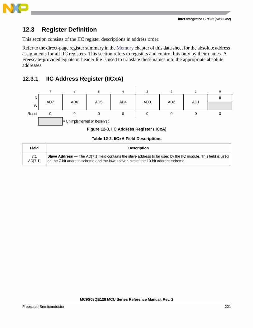
Inter-Integrated Circuit (S08IICV2)
12.3 Register DefinitionThis section consists of the IIC register descriptions in address order.
Refer to the direct-page register summary in the Memory chapter of this data sheet for the absolute addressassignments for all IIC registers. This section refers to registers and control bits only by their names. AFreescale-provided equate or header file is used to translate these names into the appropriate absoluteaddresses.
12.3.1 IIC Address Register (IICxA)
7 6 5 4 3 2 1 0
RAD7 AD6 AD5 AD4 AD3 AD2 AD1
0
W
Reset 0 0 0 0 0 0 0 0
= Unimplemented or Reserved
Figure 12-3. IIC Address Register (IICxA)
Table 12-2. IICxA Field Descriptions
Field Description
7:1AD[7:1]
Slave Address — The AD[7:1] field contains the slave address to be used by the IIC module. This field is usedon the 7-bit address scheme and the lower seven bits of the 10-bit address scheme.
MC9S08QE128 MCU Series Reference Manual, Rev. 2
Freescale Semiconductor 221
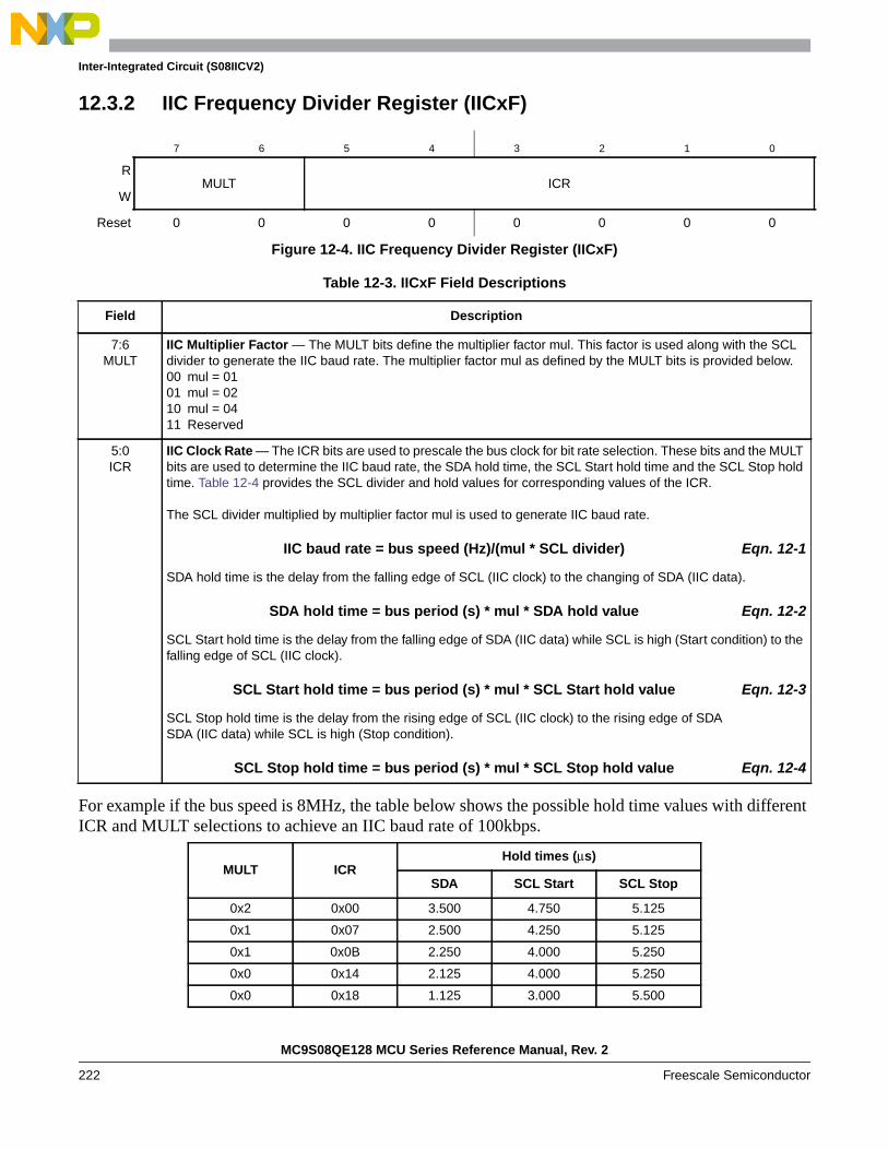
Inter-Integrated Circuit (S08IICV2)
12.3.2 IIC Frequency Divider Register (IICxF)
For example if the bus speed is 8MHz, the table below shows the possible hold time values with differentICR and MULT selections to achieve an IIC baud rate of 100kbps.
7 6 5 4 3 2 1 0
RMULT ICR
W
Reset 0 0 0 0 0 0 0 0
Figure 12-4. IIC Frequency Divider Register (IICxF)
Table 12-3. IICxF Field Descriptions
Field Description
7:6MULT
IIC Multiplier Factor — The MULT bits define the multiplier factor mul. This factor is used along with the SCLdivider to generate the IIC baud rate. The multiplier factor mul as defined by the MULT bits is provided below.00 mul = 0101 mul = 0210 mul = 0411 Reserved
5:0ICR
IIC Clock Rate — The ICR bits are used to prescale the bus clock for bit rate selection. These bits and the MULTbits are used to determine the IIC baud rate, the SDA hold time, the SCL Start hold time and the SCL Stop holdtime. Table 12-4 provides the SCL divider and hold values for corresponding values of the ICR.
The SCL divider multiplied by multiplier factor mul is used to generate IIC baud rate.
IIC baud rate = bus speed (Hz)/(mul * SCL divider) Eqn. 12-1
SDA hold time is the delay from the falling edge of SCL (IIC clock) to the changing of SDA (IIC data).
SDA hold time = bus period (s) * mul * SDA hold value Eqn. 12-2
SCL Start hold time is the delay from the falling edge of SDA (IIC data) while SCL is high (Start condition) to thefalling edge of SCL (IIC clock).
SCL Start hold time = bus period (s) * mul * SCL Start hold value Eqn. 12-3
SCL Stop hold time is the delay from the rising edge of SCL (IIC clock) to the rising edge of SDASDA (IIC data) while SCL is high (Stop condition).
SCL Stop hold time = bus period (s) * mul * SCL Stop hold value Eqn. 12-4
MULT ICRHold times (μs)
SDA SCL Start SCL Stop
0x2 0x00 3.500 4.750 5.125
0x1 0x07 2.500 4.250 5.125
0x1 0x0B 2.250 4.000 5.250
0x0 0x14 2.125 4.000 5.250
0x0 0x18 1.125 3.000 5.500
MC9S08QE128 MCU Series Reference Manual, Rev. 2
222 Freescale Semiconductor
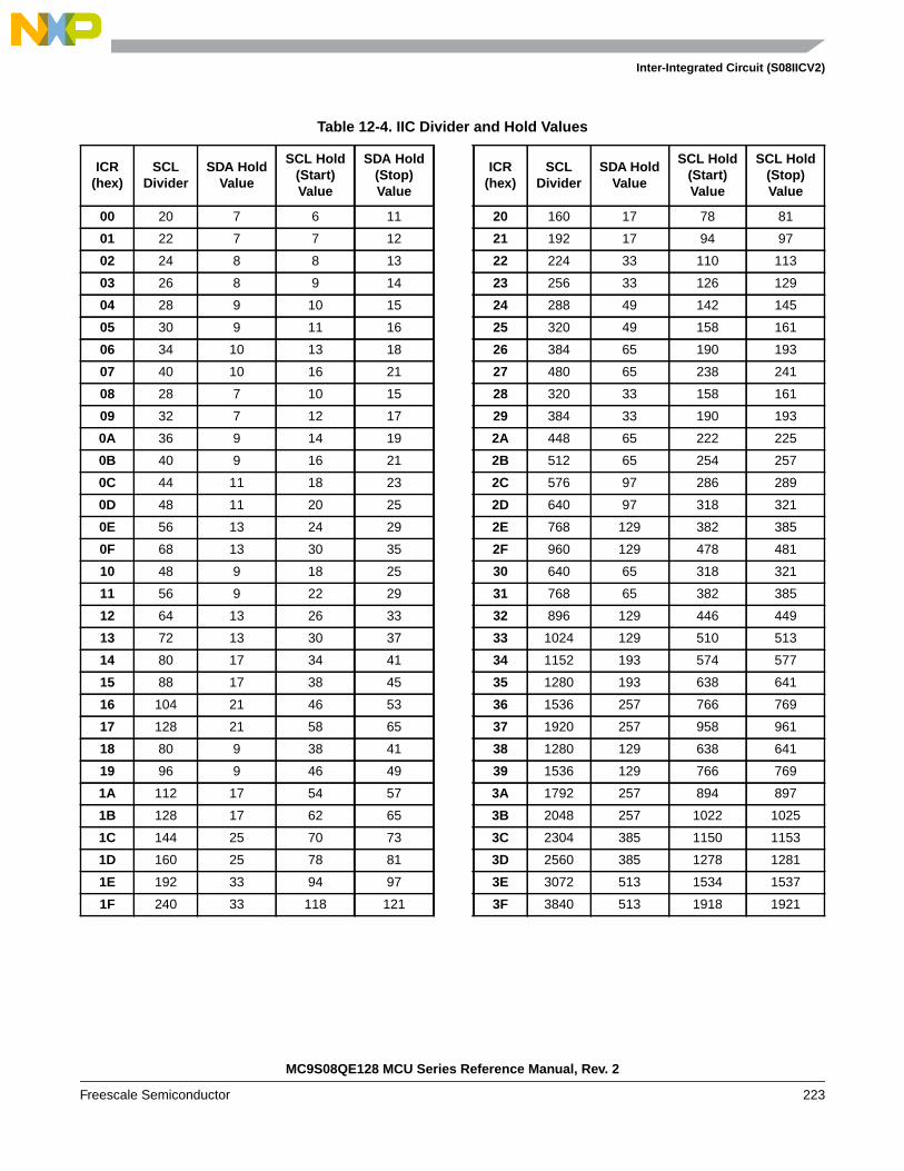
Inter-Integrated Circuit (S08IICV2)
Table 12-4. IIC Divider and Hold Values
ICR(hex)
SCLDivider
SDA HoldValue
SCL Hold(Start)Value
SDA Hold(Stop)Value
ICR(hex)
SCLDivider
SDA HoldValue
SCL Hold(Start)Value
SCL Hold(Stop)Value
00 20 7 6 11 20 160 17 78 81
01 22 7 7 12 21 192 17 94 97
02 24 8 8 13 22 224 33 110 113
03 26 8 9 14 23 256 33 126 129
04 28 9 10 15 24 288 49 142 145
05 30 9 11 16 25 320 49 158 161
06 34 10 13 18 26 384 65 190 193
07 40 10 16 21 27 480 65 238 241
08 28 7 10 15 28 320 33 158 161
09 32 7 12 17 29 384 33 190 193
0A 36 9 14 19 2A 448 65 222 225
0B 40 9 16 21 2B 512 65 254 257
0C 44 11 18 23 2C 576 97 286 289
0D 48 11 20 25 2D 640 97 318 321
0E 56 13 24 29 2E 768 129 382 385
0F 68 13 30 35 2F 960 129 478 481
10 48 9 18 25 30 640 65 318 321
11 56 9 22 29 31 768 65 382 385
12 64 13 26 33 32 896 129 446 449
13 72 13 30 37 33 1024 129 510 513
14 80 17 34 41 34 1152 193 574 577
15 88 17 38 45 35 1280 193 638 641
16 104 21 46 53 36 1536 257 766 769
17 128 21 58 65 37 1920 257 958 961
18 80 9 38 41 38 1280 129 638 641
19 96 9 46 49 39 1536 129 766 769
1A 112 17 54 57 3A 1792 257 894 897
1B 128 17 62 65 3B 2048 257 1022 1025
1C 144 25 70 73 3C 2304 385 1150 1153
1D 160 25 78 81 3D 2560 385 1278 1281
1E 192 33 94 97 3E 3072 513 1534 1537
1F 240 33 118 121 3F 3840 513 1918 1921
MC9S08QE128 MCU Series Reference Manual, Rev. 2
Freescale Semiconductor 223

Inter-Integrated Circuit (S08IICV2)
12.3.3 IIC Control Register (IICxC1)
7 6 5 4 3 2 1 0
RIICEN IICIE MST TX TXAK
0 0 0
W RSTA
Reset 0 0 0 0 0 0 0 0
= Unimplemented or Reserved
Figure 12-5. IIC Control Register (IICxC1)
Table 12-5. IICxC1 Field Descriptions
Field Description
7IICEN
IIC Enable — The IICEN bit determines whether the IIC module is enabled.0 IIC is not enabled.1 IIC is enabled.
6IICIE
IIC Interrupt Enable — The IICIE bit determines whether an IIC interrupt is requested.0 IIC interrupt request not enabled.1 IIC interrupt request enabled.
5MST
Master Mode Select — The MST bit is changed from a 0 to a 1 when a START signal is generated on the busand master mode is selected. When this bit changes from a 1 to a 0 a STOP signal is generated and the modeof operation changes from master to slave.0 Slave mode.1 Master mode.
4TX
Transmit Mode Select — The TX bit selects the direction of master and slave transfers. In master mode this bitshould be set according to the type of transfer required. Therefore, for address cycles, this bit will always be high.When addressed as a slave this bit should be set by software according to the SRW bit in the status register.0 Receive.1 Transmit.
3TXAK
Transmit Acknowledge Enable — This bit specifies the value driven onto the SDA during data acknowledgecycles for both master and slave receivers.0 An acknowledge signal will be sent out to the bus after receiving one data byte.1 No acknowledge signal response is sent.
2RSTA
Repeat START — Writing a 1 to this bit will generate a repeated START condition provided it is the currentmaster. This bit will always be read as a low. Attempting a repeat at the wrong time will result in loss of arbitration.
MC9S08QE128 MCU Series Reference Manual, Rev. 2
224 Freescale Semiconductor
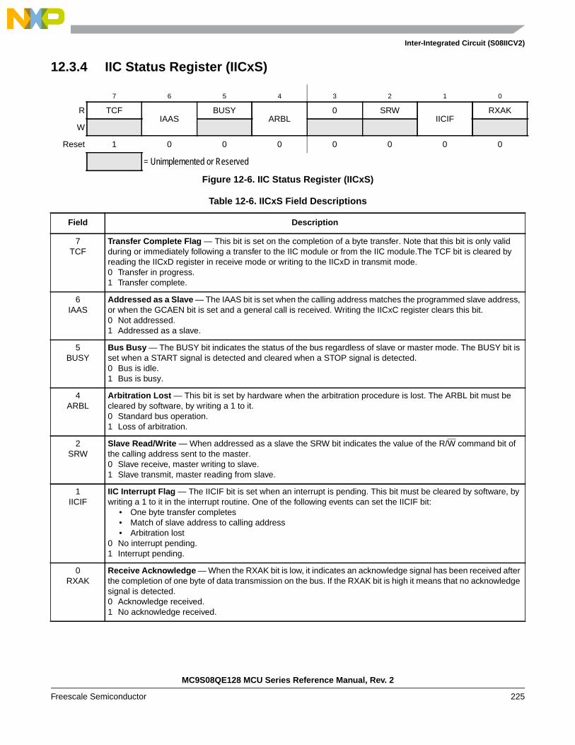
Inter-Integrated Circuit (S08IICV2)
12.3.4 IIC Status Register (IICxS)
7 6 5 4 3 2 1 0
R TCFIAAS
BUSYARBL
0 SRWIICIF
RXAK
W
Reset 1 0 0 0 0 0 0 0
= Unimplemented or Reserved
Figure 12-6. IIC Status Register (IICxS)
Table 12-6. IICxS Field Descriptions
Field Description
7TCF
Transfer Complete Flag — This bit is set on the completion of a byte transfer. Note that this bit is only validduring or immediately following a transfer to the IIC module or from the IIC module.The TCF bit is cleared byreading the IICxD register in receive mode or writing to the IICxD in transmit mode.0 Transfer in progress.1 Transfer complete.
6IAAS
Addressed as a Slave — The IAAS bit is set when the calling address matches the programmed slave address,or when the GCAEN bit is set and a general call is received. Writing the IICxC register clears this bit.0 Not addressed.1 Addressed as a slave.
5BUSY
Bus Busy — The BUSY bit indicates the status of the bus regardless of slave or master mode. The BUSY bit isset when a START signal is detected and cleared when a STOP signal is detected.0 Bus is idle.1 Bus is busy.
4ARBL
Arbitration Lost — This bit is set by hardware when the arbitration procedure is lost. The ARBL bit must becleared by software, by writing a 1 to it.0 Standard bus operation.1 Loss of arbitration.
2SRW
Slave Read/Write — When addressed as a slave the SRW bit indicates the value of the R/W command bit ofthe calling address sent to the master.0 Slave receive, master writing to slave.1 Slave transmit, master reading from slave.
1IICIF
IIC Interrupt Flag — The IICIF bit is set when an interrupt is pending. This bit must be cleared by software, bywriting a 1 to it in the interrupt routine. One of the following events can set the IICIF bit:
• One byte transfer completes• Match of slave address to calling address• Arbitration lost
0 No interrupt pending.1 Interrupt pending.
0RXAK
Receive Acknowledge — When the RXAK bit is low, it indicates an acknowledge signal has been received afterthe completion of one byte of data transmission on the bus. If the RXAK bit is high it means that no acknowledgesignal is detected.0 Acknowledge received.1 No acknowledge received.
MC9S08QE128 MCU Series Reference Manual, Rev. 2
Freescale Semiconductor 225
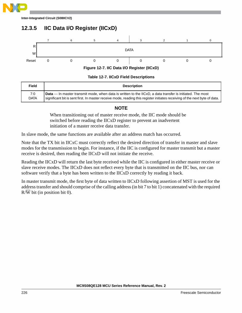
Inter-Integrated Circuit (S08IICV2)
12.3.5 IIC Data I/O Register (IICxD)
NOTEWhen transitioning out of master receive mode, the IIC mode should beswitched before reading the IICxD register to prevent an inadvertentinitiation of a master receive data transfer.
In slave mode, the same functions are available after an address match has occurred.
Note that the TX bit in IICxC must correctly reflect the desired direction of transfer in master and slavemodes for the transmission to begin. For instance, if the IIC is configured for master transmit but a masterreceive is desired, then reading the IICxD will not initiate the receive.
Reading the IICxD will return the last byte received while the IIC is configured in either master receive orslave receive modes. The IICxD does not reflect every byte that is transmitted on the IIC bus, nor cansoftware verify that a byte has been written to the IICxD correctly by reading it back.
In master transmit mode, the first byte of data written to IICxD following assertion of MST is used for theaddress transfer and should comprise of the calling address (in bit 7 to bit 1) concatenated with the requiredR/W bit (in position bit 0).
7 6 5 4 3 2 1 0
RDATA
W
Reset 0 0 0 0 0 0 0 0
Figure 12-7. IIC Data I/O Register (IICxD)
Table 12-7. IICxD Field Descriptions
Field Description
7:0DATA
Data — In master transmit mode, when data is written to the IICxD, a data transfer is initiated. The mostsignificant bit is sent first. In master receive mode, reading this register initiates receiving of the next byte of data.
MC9S08QE128 MCU Series Reference Manual, Rev. 2
226 Freescale Semiconductor

Inter-Integrated Circuit (S08IICV2)
12.3.6 IIC Control Register 2 (IICxC2)
7 6 5 4 3 2 1 0
RGCAEN ADEXT
0 0 0AD10 AD9 AD8
W
Reset 0 0 0 0 0 0 0 0
= Unimplemented or Reserved
Figure 12-8. IIC Control Register (IICxC2)
Table 12-8. IICxC2 Field Descriptions
Field Description
7GCAEN
General Call Address Enable — The GCAEN bit enables or disables general call address.0 General call address is disabled1 General call address is enabled.
6ADEXT
Address Extension — The ADEXT bit controls the number of bits used for the slave address.0 7-bit address scheme1 10-bit address scheme
2:0AD[10:8]
Slave Address — The AD[10:8] field contains the upper three bits of the slave address in the 10-bit addressscheme. This field is only valid when the ADEXT bit is set.
MC9S08QE128 MCU Series Reference Manual, Rev. 2
Freescale Semiconductor 227

Inter-Integrated Circuit (S08IICV2)
12.4 Functional DescriptionThis section provides a complete functional description of the IIC module.
12.4.1 IIC Protocol
The IIC bus system uses a serial data line (SDA) and a serial clock line (SCL) for data transfer. All devicesconnected to it must have open drain or open collector outputs. A logic AND function is exercised on bothlines with external pull-up resistors. The value of these resistors is system dependent.
Normally, a standard communication is composed of four parts:
• START signal
• Slave address transmission
• Data transfer
• STOP signal
The STOP signal should not be confused with the CPU STOP instruction. The IIC bus systemcommunication is described briefly in the following sections and illustrated in Figure 12-9.
Figure 12-9. IIC Bus Transmission Signals
SCL
SDA
STARTSIGNAL
ACKBIT
1 2 3 4 5 6 7 8
MSB LSB
1 2 3 4 5 6 7 8
MSB LSB
STOPSIGNAL
NO
SCL
SDA
1 2 3 4 5 6 7 8
MSB LSB
1 2 5 6 7 8
MSB LSB
REPEATED
3 4
9 9
AD7 AD6 AD5 AD4 AD3 AD2 AD1 R/W XXX D7 D6 D5 D4 D3 D2 D1 D0
CALLING ADDRESS READ/ DATA BYTE
AD7 AD6 AD5 AD4 AD3 AD2 AD1 R/W AD7 AD6 AD5 AD4 AD3 AD2 AD1 R/W
NEW CALLING ADDRESS
9 9
XX
ACKBITWRITE
STARTSIGNAL
STARTSIGNAL
ACKBIT
CALLING ADDRESS READ/WRITE
STOPSIGNAL
NOACKBIT
READ/WRITE
MC9S08QE128 MCU Series Reference Manual, Rev. 2
228 Freescale Semiconductor
Inter-Integrated Circuit (S08IICV2)
12.4.1.1 START Signal
When the bus is free; i.e., no master device is engaging the bus (both SCL and SDA lines are at logicalhigh), a master may initiate communication by sending a START signal. As shown in Figure 12-9, aSTART signal is defined as a high-to-low transition of SDA while SCL is high. This signal denotes thebeginning of a new data transfer (each data transfer may contain several bytes of data) and brings all slavesout of their idle states.
12.4.1.2 Slave Address Transmission
The first byte of data transferred immediately after the START signal is the slave address transmitted bythe master. This is a seven-bit calling address followed by a R/W bit. The R/W bit tells the slave the desireddirection of data transfer.
1 = Read transfer, the slave transmits data to the master.0 = Write transfer, the master transmits data to the slave.
Only the slave with a calling address that matches the one transmitted by the master will respond bysending back an acknowledge bit. This is done by pulling the SDA low at the 9th clock (see Figure 12-9).
No two slaves in the system may have the same address. If the IIC module is the master, it must not transmitan address that is equal to its own slave address. The IIC cannot be master and slave at the same time.However, if arbitration is lost during an address cycle, the IIC will revert to slave mode and operatecorrectly even if it is being addressed by another master.
12.4.1.3 Data Transfer
Before successful slave addressing is achieved, the data transfer can proceed byte-by-byte in a directionspecified by the R/W bit sent by the calling master.
All transfers that come after an address cycle are referred to as data transfers, even if they carry sub-addressinformation for the slave device
Each data byte is 8 bits long. Data may be changed only while SCL is low and must be held stable whileSCL is high as shown in Figure 12-9. There is one clock pulse on SCL for each data bit, the MSB beingtransferred first. Each data byte is followed by a 9th (acknowledge) bit, which is signalled from thereceiving device. An acknowledge is signalled by pulling the SDA low at the ninth clock. In summary, onecomplete data transfer needs nine clock pulses.
If the slave receiver does not acknowledge the master in the 9th bit time, the SDA line must be left highby the slave. The master interprets the failed acknowledge as an unsuccessful data transfer.
If the master receiver does not acknowledge the slave transmitter after a data byte transmission, the slaveinterprets this as an end of data transfer and releases the SDA line.
In either case, the data transfer is aborted and the master does one of two things:
• Relinquishes the bus by generating a STOP signal.
• Commences a new calling by generating a repeated START signal.
MC9S08QE128 MCU Series Reference Manual, Rev. 2
Freescale Semiconductor 229

Inter-Integrated Circuit (S08IICV2)
12.4.1.4 STOP Signal
The master can terminate the communication by generating a STOP signal to free the bus. However, themaster may generate a START signal followed by a calling command without generating a STOP signalfirst. This is called repeated START. A STOP signal is defined as a low-to-high transition of SDA whileSCL at logical 1 (see Figure 12-9).
The master can generate a STOP even if the slave has generated an acknowledge at which point the slavemust release the bus.
12.4.1.5 Repeated START Signal
As shown in Figure 12-9, a repeated START signal is a START signal generated without first generating aSTOP signal to terminate the communication. This is used by the master to communicate with anotherslave or with the same slave in different mode (transmit/receive mode) without releasing the bus.
12.4.1.6 Arbitration Procedure
The IIC bus is a true multi-master bus that allows more than one master to be connected on it. If two ormore masters try to control the bus at the same time, a clock synchronization procedure determines the busclock, for which the low period is equal to the longest clock low period and the high is equal to the shortestone among the masters. The relative priority of the contending masters is determined by a data arbitrationprocedure, a bus master loses arbitration if it transmits logic 1 while another master transmits logic 0. Thelosing masters immediately switch over to slave receive mode and stop driving SDA output. In this case,the transition from master to slave mode does not generate a STOP condition. Meanwhile, a status bit isset by hardware to indicate loss of arbitration.
12.4.1.7 Clock Synchronization
Because wire-AND logic is performed on the SCL line, a high-to-low transition on the SCL line affects allthe devices connected on the bus. The devices start counting their low period and after a device’s clock hasgone low, it holds the SCL line low until the clock high state is reached. However, the change of low tohigh in this device clock may not change the state of the SCL line if another device clock is still within itslow period. Therefore, synchronized clock SCL is held low by the device with the longest low period.Devices with shorter low periods enter a high wait state during this time (see Figure 12-10). When alldevices concerned have counted off their low period, the synchronized clock SCL line is released andpulled high. There is then no difference between the device clocks and the state of the SCL line and all thedevices start counting their high periods. The first device to complete its high period pulls the SCL linelow again.
MC9S08QE128 MCU Series Reference Manual, Rev. 2
230 Freescale Semiconductor

Inter-Integrated Circuit (S08IICV2)
Figure 12-10. IIC Clock Synchronization
12.4.1.8 Handshaking
The clock synchronization mechanism can be used as a handshake in data transfer. Slave devices may holdthe SCL low after completion of one byte transfer (9 bits). In such case, it halts the bus clock and forcesthe master clock into wait states until the slave releases the SCL line.
12.4.1.9 Clock Stretching
The clock synchronization mechanism can be used by slaves to slow down the bit rate of a transfer. Afterthe master has driven SCL low the slave can drive SCL low for the required period and then release it. Ifthe slave SCL low period is greater than the master SCL low period then the resulting SCL bus signal lowperiod is stretched.
SCL1
SCL2
SCL
INTERNAL COUNTER RESET
DELAY START COUNTING HIGH PERIOD
MC9S08QE128 MCU Series Reference Manual, Rev. 2
Freescale Semiconductor 231

Inter-Integrated Circuit (S08IICV2)
12.4.2 10-bit Address
For 10-bit addressing, 0x11110 is used for the first 5 bits of the first address byte. Various combinations ofread/write formats are possible within a transfer that includes 10-bit addressing.
12.4.2.1 Master-Transmitter Addresses a Slave-Receiver
The transfer direction is not changed (see Table 12-9). When a 10-bit address follows a START condition,each slave compares the first seven bits of the first byte of the slave address (11110XX) with its ownaddress and tests whether the eighth bit (R/W direction bit) is 0. It is possible that more than one devicewill find a match and generate an acknowledge (A1). Each slave that finds a match will compare the eightbits of the second byte of the slave address with its own address, but only one slave will find a match andgenerate an acknowledge (A2). The matching slave will remain addressed by the master until it receivesa STOP condition (P) or a repeated START condition (Sr) followed by a different slave address.
After the master-transmitter has sent the first byte of the 10-bit address, the slave-receiver will see an IICinterrupt. User software must ensure that for this interrupt, the contents of IICD are ignored and not treatedas valid data.
12.4.2.2 Master-Receiver Addresses a Slave-Transmitter
The transfer direction is changed after the second R/W bit (see Table 12-10). Up to and includingacknowledge bit A2, the procedure is the same as that described for a master-transmitter addressing aslave-receiver. After the repeated START condition (Sr), a matching slave remembers that it was addressedbefore. This slave then checks whether the first seven bits of the first byte of the slave address followingSr are the same as they were after the START condition (S), and tests whether the eighth (R/W) bit is 1. Ifthere is a match, the slave considers that it has been addressed as a transmitter and generates acknowledgeA3. The slave-transmitter remains addressed until it receives a STOP condition (P) or a repeated STARTcondition (Sr) followed by a different slave address.
After a repeated START condition (Sr), all other slave devices will also compare the first seven bits of thefirst byte of the slave address with their own addresses and test the eighth (R/W) bit. However, none ofthem will be addressed because R/W = 1 (for 10-bit devices), or the 11110XX slave address (for 7-bitdevices) does not match.
After the master-receiver has sent the first byte of the 10-bit address, the slave-transmitter will see an IICinterrupt. User software must ensure that for this interrupt, the contents of IICD are ignored and not treatedas valid data.
SSlave Address 1st 7 bits R/W
A1Slave Address 2nd byte
A2 Data A ... Data A/A P11110 + AD10 + AD9 0 AD[8:1]
Table 12-9. Master-Transmitter Addresses Slave-Receiver with a 10-bit Address
SSlave Address
1st 7 bitsR/W
A1Slave Address
2nd byte A2 SrSlave Address
1st 7 bitsR/W
A3 Data A ... Data A P
11110 + AD10 + AD9 0 AD[8:1] 11110 + AD10 + AD9 1
Table 12-10. Master-Receiver Addresses a Slave-Transmitter with a 10-bit Address
MC9S08QE128 MCU Series Reference Manual, Rev. 2
232 Freescale Semiconductor
Inter-Integrated Circuit (S08IICV2)
12.4.3 General Call Address
General calls can be requested in 7-bit address or 10-bit address. If the GCAEN bit is set, the IIC matchesthe general call address as well as its own slave address. When the IIC responds to a general call, it acts asa slave-receiver and the IAAS bit is set after the address cycle. Software must read the IICD register afterthe first byte transfer to determine whether the address matches is its own slave address or a general call.If the value is “00”, the match is a general call. If the GCAEN bit is clear, the IIC ignores any data suppliedfrom a general call address by not issuing an acknowledgement.
12.5 ResetsThe IIC is disabled after reset. The IIC cannot cause an MCU reset.
12.6 InterruptsThe IIC generates a single interrupt.
An interrupt from the IIC is generated when any of the events in Table 12-11 occur, provided the IICIE bitis set. The interrupt is driven by bit IICIF (of the IIC status register) and masked with bit IICIE (of the IICcontrol register). The IICIF bit must be cleared by software by writing a 1 to it in the interrupt routine. Theuser can determine the interrupt type by reading the status register.
12.6.1 Byte Transfer Interrupt
The TCF (transfer complete flag) bit is set at the falling edge of the 9th clock to indicate the completion ofbyte transfer.
12.6.2 Address Detect Interrupt
When the calling address matches the programmed slave address (IIC address register) or when theGCAEN bit is set and a general call is received, the IAAS bit in the status register is set. The CPU isinterrupted, provided the IICIE is set. The CPU must check the SRW bit and set its Tx mode accordingly.
12.6.3 Arbitration Lost Interrupt
The IIC is a true multi-master bus that allows more than one master to be connected on it. If two or moremasters try to control the bus at the same time, the relative priority of the contending masters is determinedby a data arbitration procedure. The IIC module asserts this interrupt when it loses the data arbitrationprocess and the ARBL bit in the status register is set.
Arbitration is lost in the following circumstances:
Table 12-11. Interrupt Summary
Interrupt Source Status Flag Local Enable
Complete 1-byte transfer TCF IICIF IICIE
Match of received calling address IAAS IICIF IICIE
Arbitration Lost ARBL IICIF IICIE
MC9S08QE128 MCU Series Reference Manual, Rev. 2
Freescale Semiconductor 233

Inter-Integrated Circuit (S08IICV2)
• SDA sampled as a low when the master drives a high during an address or data transmit cycle.
• SDA sampled as a low when the master drives a high during the acknowledge bit of a data receivecycle.
• A START cycle is attempted when the bus is busy.
• A repeated START cycle is requested in slave mode.
• A STOP condition is detected when the master did not request it.
This bit must be cleared by software by writing a 1 to it.
MC9S08QE128 MCU Series Reference Manual, Rev. 2
234 Freescale Semiconductor
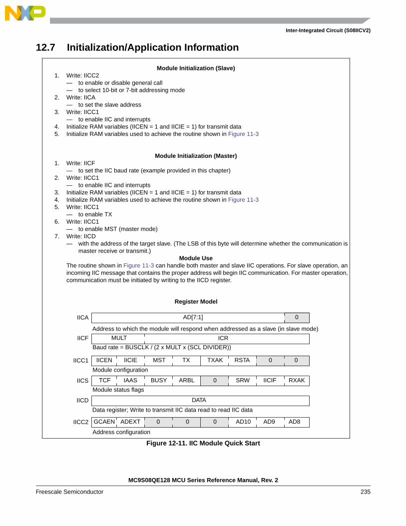
Inter-Integrated Circuit (S08IICV2)
12.7 Initialization/Application Information
Figure 12-11. IIC Module Quick Start
Module Initialization (Slave)1. Write: IICC2
— to enable or disable general call— to select 10-bit or 7-bit addressing mode
2. Write: IICA— to set the slave address
3. Write: IICC1— to enable IIC and interrupts
4. Initialize RAM variables (IICEN = 1 and IICIE = 1) for transmit data5. Initialize RAM variables used to achieve the routine shown in Figure 11-3
Module Initialization (Master)1. Write: IICF
— to set the IIC baud rate (example provided in this chapter)2. Write: IICC1
— to enable IIC and interrupts3. Initialize RAM variables (IICEN = 1 and IICIE = 1) for transmit data4. Initialize RAM variables used to achieve the routine shown in Figure 11-35. Write: IICC1
— to enable TX6. Write: IICC1
— to enable MST (master mode)7. Write: IICD
— with the address of the target slave. (The LSB of this byte will determine whether the communication ismaster receive or transmit.)
Module UseThe routine shown in Figure 11-3 can handle both master and slave IIC operations. For slave operation, anincoming IIC message that contains the proper address will begin IIC communication. For master operation,communication must be initiated by writing to the IICD register.
0
IICF
IICA
Baud rate = BUSCLK / (2 x MULT x (SCL DIVIDER))
TX TXAK RSTA 0 0IICC1 IICEN IICIE MST
Module configuration
ARBL 0 SRW IICIF RXAKIICS TCF IAAS BUSY
Module status flags
Register Model
AD[7:1]
Address to which the module will respond when addressed as a slave (in slave mode)
MULT ICR
IICD DATA
Data register; Write to transmit IIC data read to read IIC data
0 AD10 AD9 AD8IICC2 GCAEN ADEXT
Address configuration
00
MC9S08QE128 MCU Series Reference Manual, Rev. 2
Freescale Semiconductor 235
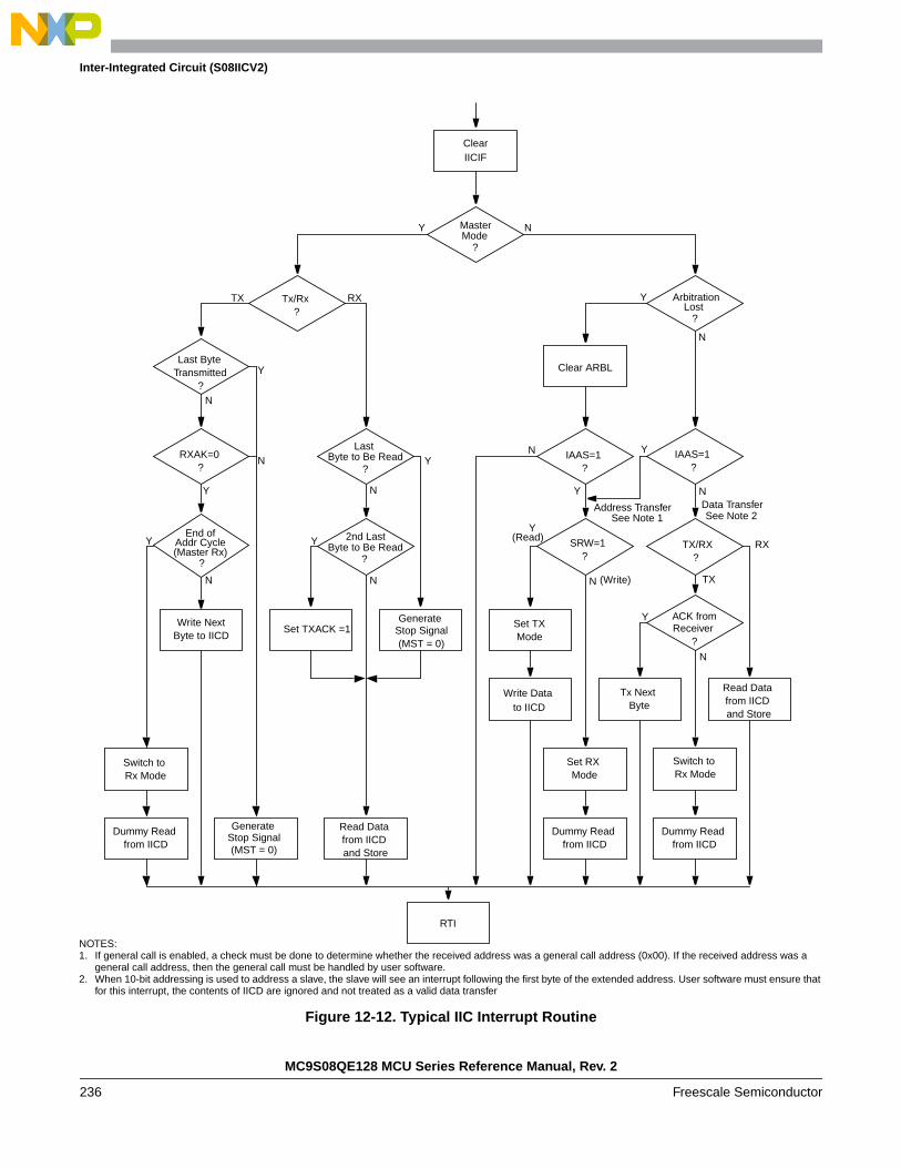
Inter-Integrated Circuit (S08IICV2)
Figure 12-12. Typical IIC Interrupt Routine
Clear
MasterMode
?
Tx/Rx?
Last ByteTransmitted
?
RXAK=0?
End ofAddr Cycle(Master Rx)
?
Write NextByte to IICD
Switch toRx Mode
Dummy Readfrom IICD
GenerateStop Signal
Read Datafrom IICDand Store
Set TXACK =1Generate
Stop Signal
2nd LastByte to Be Read
?
LastByte to Be Read
?
ArbitrationLost
?
Clear ARBL
IAAS=1?
IAAS=1?
SRW=1?
TX/RX?
Set TXMode
Write Datato IICD
Set RXMode
Dummy Readfrom IICD
ACK fromReceiver
?
Tx NextByte
Read Datafrom IICDand Store
Switch toRx Mode
Dummy Readfrom IICD
RTI
Y N
Y
Y Y
Y
Y
Y
Y
Y
Y
N
N
N
NN
N
N
N
N
Y
TX RX
RX
TX(Write)
(Read)
N
IICIF
Address Transfer Data Transfer
(MST = 0)
(MST = 0)
See Note 1
NOTES:1. If general call is enabled, a check must be done to determine whether the received address was a general call address (0x00). If the received address was a
general call address, then the general call must be handled by user software.2. When 10-bit addressing is used to address a slave, the slave will see an interrupt following the first byte of the extended address. User software must ensure that
for this interrupt, the contents of IICD are ignored and not treated as a valid data transfer
See Note 2
MC9S08QE128 MCU Series Reference Manual, Rev. 2
236 Freescale Semiconductor
Chapter 13Real-Time Counter (S08RTCV1)
13.1 IntroductionThe real-time counter (RTC) consists of one 8-bit counter, one 8-bit comparator, several binary-based anddecimal-based prescaler dividers, three clock sources, and one programmable periodic interrupt. Thismodule can be used for time-of-day, calendar, or any task scheduling functions. It can also serve as a cyclicwake up from low power modes without the need of external components.
13.1.1 ADC Hardware Trigger
The RTC can be enabled as a hardware trigger for the ADC module by setting ADCSC2[ADTRG]. Whenenabled, the ADC is triggered each time RTCINT matches RTCMOD. The RTC interrupt does not have tobe enabled to trigger the ADC.
13.1.2 RTC Clock Sources
The RTC module on MC9S08QE128 Series can be clocked from ICSIRCLK, OSCOUT, or the LPO.
In this chapter, ERCLK is replaced by OSCOUT for this MCU.
13.1.3 RTC Modes of Operation
All clock sources are available in all modes except stop2. The OSCOUT and LPO can be enabled as theclock source of the RTC in stop2.
13.1.3.1 RTC Status after Stop2 Wakeup
The registers associated with the RTC are unaffected after a stop2 wakeup.
13.1.3.2 Clocks in Stop Modes
In the MC9S08QE128 Series, LPO and OSCOUT can be used in stop2 and stop3. IRCLK is available onlyin stop3.
13.1.4 RTC Clock Gating
The bus clock to the RTC can be gated on and off with SCGC2[RTC]. This bit is set after any reset, whichenables the bus clock to this module. To conserve power, the RTC bit can be cleared to disable the clockto this module when not in use. See Section 5.7, “Peripheral Clock Gating,” for details.
MC9S08QE128 MCU Series Reference Manual, Rev. 2
Freescale Semiconductor 237

Chapter 13 Real-Time Counter (S08RTCV1)
13.1.5 Interrupt Vector
See Section 4.2, “Reset and Interrupt Vector Assignments,” for the RTC interrupt vector assignment.
MC9S08QE128 MCU Series Reference Manual, Rev. 2
238 Freescale Semiconductor
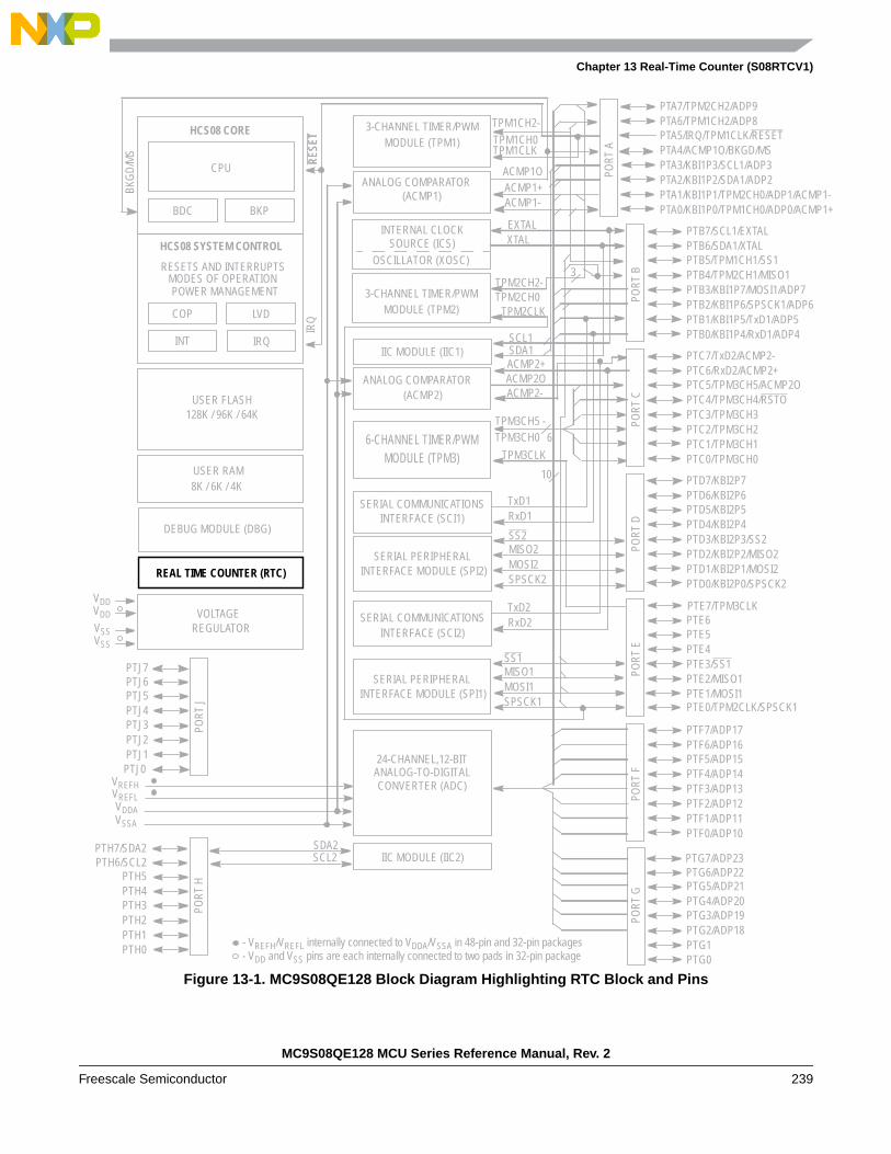
Chapter 13 Real-Time Counter (S08RTCV1)
-+
Figure 13-1. MC9S08QE128 Block Diagram Highlighting RTC Block and Pins
TPM2CH2-TPM2CH0
TPM1CH0
TPM1CH2-
ANALOG COMPARATOR(ACMP1)
ACMP1O
ACMP1-ACMP1+
VSS
VDD
IIC MODULE (IIC1)
SERIAL PERIPHERAL INTERFACE MODULE (SPI1)
USER FLASH
USER RAM
128K / 96K / 64K
HCS08 CORE
CPU
BDC
6-CHANNEL TIMER/PWMMODULE (TPM3)
HCS08 SYSTEM CONTROL
RESETS AND INTERRUPTSMODES OF OPERATIONPOWER MANAGEMENT
VOLTAGEREGULATOR
COP
IRQ
LVD
OSCILLATOR (XOSC)
RES
ET
VREFL
VREFH
8K / 6K / 4K
BKG
D/M
S
INTERFACE (SCI1)SERIAL COMMUNICATIONS
MISO1SS1
SPSCK1
3-CHANNEL TIMER/PWMMODULE (TPM2)
REAL TIME COUNTER (RTC)
DEBUG MODULE (DBG)
IRQ
PTA3/KBI1P3/SCL1/ADP3PTA4/ACMP1O/BKGD/MSPTA5/IRQ/TPM1CLK/RESET
PTA2/KBI1P2/SDA1/ADP2PTA1/KBI1P1/TPM2CH0/ADP1/ACMP1PTA0/KBI1P0/TPM1CH0/ADP0/ACMP1
PORT
A
PTA6/TPM1CH2/ADP8PTA7/TPM2CH2/ADP9
MOSI1
PTB3/KBI1P7/MOSI1/ADP7PTB4/TPM2CH1/MISO1PTB5/TPM1CH1/SS1
PTB2/KBI1P6/SPSCK1/ADP6PTB1/KBI1P5/TxD1/ADP5PTB0/KBI1P4/RxD1/ADP4
PORT
B
PTB6/SDA1/XTALPTB7/SCL1/EXTAL
PTC3/TPM3CH3PTC4/TPM3CH4/RSTOPTC5/TPM3CH5/ACMP2O
PTC2/TPM3CH2PTC1/TPM3CH1PTC0/TPM3CH0
PORT
C
PTC6/RxD2/ACMP2+PTC7/TxD2/ACMP2-
PTD3/KBI2P3/SS2PTD4/KBI2P4PTD5/KBI2P5
PTD2/KBI2P2/MISO2PTD1/KBI2P1/MOSI2PTD0/KBI2P0/SPSCK2
PORT
D
PTD6/KBI2P6PTD7/KBI2P7
PTE3/SS1PTE4PTE5
PTE2/MISO1PTE1/MOSI1
TPM2CLK
PORT
EPTE6
PTE0/TPM2CLK/SPSCK1
PTF3/ADP13PTF4/ADP14PTF5/ADP15
PTF2/ADP12PTF1/ADP11PTF0/ADP10
PORT
F
PTF6/ADP16PTF7/ADP17
PTG1PTG2/ADP18PTG3/ADP19PO
RT G
PTG4/ADP20PTG5/ADP21
PTG0
VSS
VDD
VSSA
VDDA
BKP
INT
ANALOG COMPARATOR(ACMP2)
INTERFACE (SCI2)SERIAL COMMUNICATIONS
6TPM3CH5 -TPM3CH0
- VREFH/VREFL internally connected to VDDA/VSSA in 48-pin and 32-pin packages- VDD and VSS pins are each internally connected to two pads in 32-pin package
PTG6/ADP22PTG7/ADP23
SOURCE (ICS)INTERNAL CLOCK
RES
ET
PORT
JPO
RT H
PTJ1PTJ2PTJ3PTJ4PTJ5
PTJ0
PTJ6PTJ7
PTH1PTH2PTH3PTH4PTH5
PTH0
PTH6/SCL2PTH7/SDA2
IIC MODULE (IIC2)
ANALOG-TO-DIGITALCONVERTER (ADC)
24-CHANNEL,12-BIT
3-CHANNEL TIMER/PWMMODULE (TPM1)
SDA2SCL2
SERIAL PERIPHERAL INTERFACE MODULE (SPI2)
MISO2SS2
SPSCK2MOSI2
EXTALXTAL
10
SDA1SCL1
ACMP2-
ACMP2+ACMP2O
RxD1TxD1
RxD2TxD2
TPM3CLK
3
TPM1CLK
PTE7/TPM3CLK
MC9S08QE128 MCU Series Reference Manual, Rev. 2
Freescale Semiconductor 239

Real-Time Counter (S08RTCV1)
MC9S08QE128 MCU Series Reference Manual, Rev. 2
240 Freescale Semiconductor
13.1.6 Features
Features of the RTC module include:
• 8-bit up-counter
— 8-bit modulo match limit
— Software controllable periodic interrupt on match
• Three software selectable clock sources for input to prescaler with selectable binary-based anddecimal-based divider values
— 1-kHz internal Low Power Oscillator (LPO)
— External clock (ERCLK)
— 32-kHz internal clock (IRCLK)
13.1.7 Modes of Operation
This section defines the operation in stop, wait and background debug modes.
Wait Mode
The RTC continues to run in wait mode if enabled before executing the WAIT instruction. Therefore, theRTC can be used to bring the MCU out of wait mode if the real-time interrupt is enabled. For lowestpossible current consumption, the RTC should be stopped by software if not needed as an interrupt sourceduring wait mode.
Stop Modes
The RTC continues to run in stop2 or stop3 mode if the RTC is enabled before executing the STOPinstruction. Therefore, the RTC can be used to bring the MCU out of stop modes with no externalcomponents, if the real-time interrupt is enabled.
The LPO clock can be used in both stop2 and stop3 modes. ERCLK and IRCLK clocks are only availablein stop3 mode.
Power consumption is lower when all clock sources are disabled, but in that case the real-time interruptcannot wake up the MCU from stop modes.
Active Background Mode
The RTC suspends all counting during active background mode until the microcontroller returns to normaluser operating mode. Counting resumes from the suspended value as long as the RTCMOD register is notwritten and the RTCPS and RTCLKS bits are not altered.

Real-Time Counter (S08RTCV1)
MC9S08QE128 MCU Series Reference Manual, Rev. 2
Freescale Semiconductor 241
13.1.8 Block Diagram
The block diagram for the RTC module is shown in Figure 13-2.
Figure 13-2. Real-Time Counter (RTC) Block Diagram
13.2 External Signal DescriptionThe RTC does not include any off-chip signals.
13.3 Register DefinitionThe RTC includes a status and control register, an 8-bit counter register, and an 8-bit modulo register.
Refer to the direct-page register summary in the memory section of this data sheet for the absolute addressassignments for all RTC registers.This section refers to registers and control bits only by their names andrelative address offsets.
Table 13-1 is a summary of RTC registers.Table 13-1. RTC Register Summary
Name 7 6 5 4 3 2 1 0
RTCSCR
RTIF RTCLKS RTIE RTCPSW
RTCCNTR RTCCNT
W
RTCMODR
RTCMODW
CLOCKSOURCESELECT
PRESCALERDIVIDE-BY
8-BIT COUNTER(RTCCNT)
8-BIT MODULO(RTCMOD)
8-BIT COMPARATOR
RTIF
RTIE
BACKGROUND
VDD
RTCINTERRUPTREQUEST
D Q
RE
LPO
RTCCLOCK
MODE
ERCLK
IRCLK
RTCLKS
Write 1 toRTIF
RTCPSRTCLKS[0]

Real-Time Counter (S08RTCV1)
MC9S08QE128 MCU Series Reference Manual, Rev. 2
242 Freescale Semiconductor
13.3.1 RTC Status and Control Register (RTCSC)
RTCSC contains the real-time interrupt status flag (RTIF), the clock select bits (RTCLKS), the real-timeinterrupt enable bit (RTIE), and the prescaler select bits (RTCPS).
7 6 5 4 3 2 1 0
RRTIF RTCLKS RTIE RTCPS
W
Reset: 0 0 0 0 0 0 0 0
Figure 13-3. RTC Status and Control Register (RTCSC)
Table 13-2. RTCSC Field Descriptions
Field Description
7RTIF
Real-Time Interrupt Flag — This status bit indicates the RTC counter register reached the value in the RTCmodulo register. Writing a logic 0 has no effect. Writing a logic 1 clears the bit and the real-time interrupt request.Reset clears RTIF to 0.0 RTC counter has not reached the value in the RTC modulo register.1 RTC counter has reached the value in the RTC modulo register.
6:5RTCLKS
Real-Time Clock Source Select — These two read/write bits select the clock source input to the RTCprescaler. Changing the clock source clears the prescaler and RTCCNT counters. When selecting a clocksource, ensure that the clock source is properly enabled (if applicable) to ensure correct operation of the RTC.Reset clears RTCLKS to 00.00 Real-time clock source is the 1-kHz low power oscillator (LPO)01 Real-time clock source is the external clock (ERCLK)1x Real-time clock source is the internal clock (IRCLK)
4RTIE
Real-Time Interrupt Enable — This read/write bit enables real-time interrupts. If RTIE is set, then an interruptis generated when RTIF is set. Reset clears RTIE to 0.0 Real-time interrupt requests are disabled. Use software polling.1 Real-time interrupt requests are enabled.
3:0RTCPS
Real-Time Clock Prescaler Select — These four read/write bits select binary-based or decimal-baseddivide-by values for the clock source. See Table 13-3. Changing the prescaler value clears the prescaler andRTCCNT counters. Reset clears RTCPS to 0000.
Table 13-3. RTC Prescaler Divide-by values
RTCLKS[0]
RTCPS
0 1 2 3 4 5 6 7 8 9 10 11 12 13 14 15
0 OFF 23 25 26 27 28 29 210 1 2 22 10 24 102 5x10² 103
1 OFF 210 211 212 213 214 215 216 103 2x10³ 5x10³ 104 2x10⁴ 5x10⁴ 105 2x10⁵

Real-Time Counter (S08RTCV1)
MC9S08QE128 MCU Series Reference Manual, Rev. 2
Freescale Semiconductor 243
13.3.2 RTC Counter Register (RTCCNT)
RTCCNT is the read-only value of the current RTC count of the 8-bit counter.
13.3.3 RTC Modulo Register (RTCMOD)
7 6 5 4 3 2 1 0
R RTCCNT
W
Reset: 0 0 0 0 0 0 0 0
Figure 13-4. RTC Counter Register (RTCCNT)
Table 13-4. RTCCNT Field Description
Field Description
7:0RTCCNT
RTC Count— These eight read-only bits contain the current value of the 8-bit counter. Writes have no effect to thisregister. Reset, writing to RTCMOD, or writing different values to RTCLKS and RTCPS clear the count to 0x00.
7 6 5 4 3 2 1 0
RRTCMOD
W
Reset: 0 0 0 0 0 0 0 0
Figure 13-5. RTC Modulo Register (RTCMOD)
Table 13-5. RTCMOD Field Descriptions
Field Description
7:0RTCMOD
RTC Modulo — These eight read/write bits contain the modulo value used to reset the count to 0x00 upon acompare match and set the RTIF status bit. A value of 0x00 sets the RTIF bit on each rising edge of the prescaleroutput. Writing to RTCMOD resets the prescaler and the RTCCNT counters to 0x00. Reset sets the modulo to0x00.

Real-Time Counter (S08RTCV1)
MC9S08QE128 MCU Series Reference Manual, Rev. 2
244 Freescale Semiconductor
13.4 Functional DescriptionThe RTC is composed of a main 8-bit up-counter with an 8-bit modulo register, a clock source selector,and a prescaler block with binary-based and decimal-based selectable values. The module also containssoftware selectable interrupt logic.
After any MCU reset, the counter is stopped and reset to 0x00, the modulus register is set to 0x00, and theprescaler is off. The 1-kHz internal oscillator clock is selected as the default clock source. To start theprescaler, write any value other than zero to the prescaler select bits (RTCPS).
Three clock sources are software selectable: the low power oscillator clock (LPO), the external clock(ERCLK) and the internal clock (IRCLK). The RTC clock select bits (RTCLKS) are used to select thedesired clock source. If a different value is written to RTCLKS, the prescaler and RTCCNT counters arereset to 0x00.
RTCPS and the RTCLKS[0] bit select the desired divide-by value. If a different value is written to RTCPS,the prescaler and RTCCNT counters are reset to 0x00. Table 13-6 shows different prescaler period values.
Table 13-6. Prescaler Period
RTCPS
1-kHz internal clock
source prescaler period
(RTCLKS = 00)
1-MHz external clock
source prescaler period
(RTCLKS = 01)
32-kHz internal clock
source prescaler period
(RTCLKS = 10)
32-kHz internal clock
source prescaler period
(RTCLKS = 11)
0000 Off Off Off Off
0001 8 ms 1.024 ms 250 μs 32 ms
0010 32 ms 2.048 ms 1 ms 64 ms
0011 64 ms 4.096 ms 2 ms 128 ms
0100 128 ms 8.192 ms 4 ms 256 ms
0101 256 ms 16.4 ms 8 ms 512 ms
0110 512 ms 32.8 ms 16 ms 1.024 s
0111 1.024 s 65.5 ms 32 ms 2.048 s
1000 1 ms 1 ms 31.25 μs 31.25 ms
1001 2 ms 2 ms 62.5 μs 62.5 ms
1010 4 ms 5 ms 125 μs 156.25 ms
1011 10 ms 10 ms 312.5 μs 312.5 ms
1100 16 ms 20 ms 0.5 ms 0.625 s
1101 0.1 s 50 ms 3.125 ms 1.5625 s
1110 0.5 s 0.1 s 15.625 ms 3.125 s
1111 1 s 0.2 s 31.25 ms 6.25 s
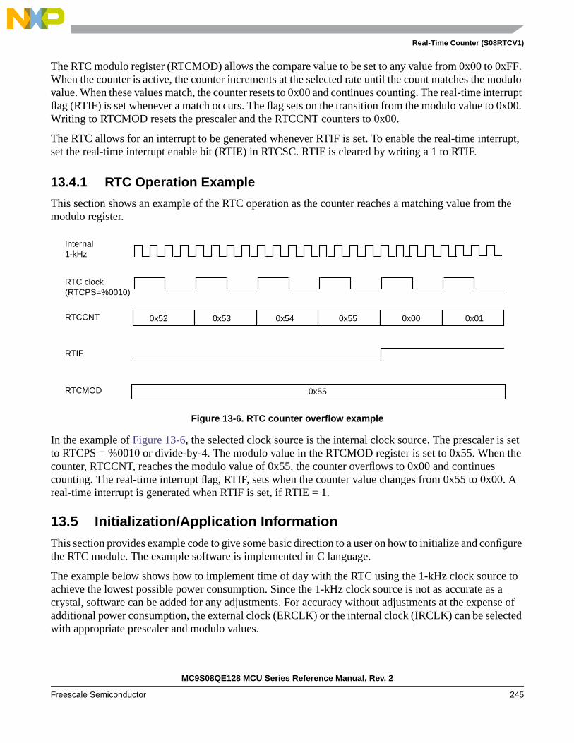
Real-Time Counter (S08RTCV1)
MC9S08QE128 MCU Series Reference Manual, Rev. 2
Freescale Semiconductor 245
The RTC modulo register (RTCMOD) allows the compare value to be set to any value from 0x00 to 0xFF.When the counter is active, the counter increments at the selected rate until the count matches the modulovalue. When these values match, the counter resets to 0x00 and continues counting. The real-time interruptflag (RTIF) is set whenever a match occurs. The flag sets on the transition from the modulo value to 0x00.Writing to RTCMOD resets the prescaler and the RTCCNT counters to 0x00.
The RTC allows for an interrupt to be generated whenever RTIF is set. To enable the real-time interrupt,set the real-time interrupt enable bit (RTIE) in RTCSC. RTIF is cleared by writing a 1 to RTIF.
13.4.1 RTC Operation Example
This section shows an example of the RTC operation as the counter reaches a matching value from themodulo register.
Figure 13-6. RTC counter overflow example
In the example of Figure 13-6, the selected clock source is the internal clock source. The prescaler is setto RTCPS = %0010 or divide-by-4. The modulo value in the RTCMOD register is set to 0x55. When thecounter, RTCCNT, reaches the modulo value of 0x55, the counter overflows to 0x00 and continuescounting. The real-time interrupt flag, RTIF, sets when the counter value changes from 0x55 to 0x00. Areal-time interrupt is generated when RTIF is set, if RTIE = 1.
13.5 Initialization/Application InformationThis section provides example code to give some basic direction to a user on how to initialize and configurethe RTC module. The example software is implemented in C language.
The example below shows how to implement time of day with the RTC using the 1-kHz clock source toachieve the lowest possible power consumption. Since the 1-kHz clock source is not as accurate as acrystal, software can be added for any adjustments. For accuracy without adjustments at the expense ofadditional power consumption, the external clock (ERCLK) or the internal clock (IRCLK) can be selectedwith appropriate prescaler and modulo values.
Internal1-kHz
RTCCNT
RTC clock(RTCPS=%0010)
RTCMOD 0x55
0x52 0x53 0x54 0x55 0x00 0x01
RTIF

Real-Time Counter (S08RTCV1)
MC9S08QE128 MCU Series Reference Manual, Rev. 2
246 Freescale Semiconductor
/* Initialize the elapsed time counters */
Seconds = 0;
Minutes = 0;
Hours = 0;
Days=0;
/* Configure RTC to interrupt every 1 second from 1-kHz clock source */
RTCMOD.byte = 0x00;
RTCSC.byte = 0x1F;
/**********************************************************************
Function Name : RTC_ISR
Notes : Interrupt service routine for RTC module.
**********************************************************************/
#pragma TRAP_PROC
void RTC_ISR(void)
{
/* Clear the interrupt flag */
RTCSC.byte = RTCSC.byte | 0x80;
/* RTC interrupts every 1 Second */
Seconds++;
/* 60 seconds in a minute */
if (Seconds > 59){
Minutes++;
Seconds = 0;
}
/* 60 minutes in an hour */
if (Minutes > 59){
Hours++;
Minutes = 0;
}
/* 24 hours in a day */
if (Hours > 23){
Days ++;
Hours = 0;
}
}
Chapter 14Serial Communications Interface (S08SCIV4)
14.1 IntroductionFigure 14-1 shows the MC9S08QE128 Series block diagram with the SCI highlighted.
NOTEIgnore any references to stop1 low-power mode in this chapter, because theMC9S08QE128 device does not support it.
14.1.1 SCI Clock Gating
The bus clock to SCI1 and SCI2 can be gated on and off using the SCGC1[SCI1,SCI2] bits, respectively.These bits are set after any reset, which enables the bus clock to these modules. To conserve power, thesebits can be cleared to disable the clock to either of these modules when not in use. See Section 5.7,“Peripheral Clock Gating,” for details.
14.1.2 Interrupt Vectors
Each SCI module contains three interrupt sources: transmit, receive, and error. See Section 4.2, “Reset andInterrupt Vector Assignments,” for a list of the SCI interrupt vector assignments.
MC9S08QE128 MCU Series Reference Manual, Rev. 2
Freescale Semiconductor 247

Chapter 14 Serial Communications Interface (S08SCIV4)
Figure 14-1. MC9S08QE128 Series Block Diagram Highlighting SCI Block and Pins
TPM2CH2-TPM2CH0
TPM1CH0
TPM1CH2-
ANALOG COMPARATOR(ACMP1)
ACMP1O
ACMP1-ACMP1+
VSS
VDD
IIC MODULE (IIC1)
SERIAL PERIPHERAL INTERFACE MODULE (SPI1)
USER FLASH
USER RAM
128K / 96K / 64K
HCS08 CORE
CPU
BDC
6-CHANNEL TIMER/PWMMODULE (TPM3)
HCS08 SYSTEM CONTROL
RESETS AND INTERRUPTSMODES OF OPERATIONPOWER MANAGEMENT
VOLTAGEREGULATOR
COP
IRQ
LVD
OSCILLATOR (XOSC)
RES
ET
VREFL
VREFH
8K / 6K / 4K
BKG
D/M
S
INTERFACE (SCI1)SERIAL COMMUNICATIONS
MISO1SS1
SPSCK1
3-CHANNEL TIMER/PWMMODULE (TPM2)
REAL TIME COUNTER (RTC)
DEBUG MODULE (DBG)
IRQ
PTA3/KBI1P3/SCL1/ADP3PTA4/ACMP1O/BKGD/MSPTA5/IRQ/TPM1CLK/RESET
PTA2/KBI1P2/SDA1/ADP2PTA1/KBI1P1/TPM2CH0/ADP1/ACMP1-PTA0/KBI1P0/TPM1CH0/ADP0/ACMP1+
PORT
A
PTA6/TPM1CH2/ADP8PTA7/TPM2CH2/ADP9
MOSI1
PTB3/KBI1P7/MOSI1/ADP7PTB4/TPM2CH1/MISO1PTB5/TPM1CH1/SS1
PTB2/KBI1P6/SPSCK1/ADP6PTB1/KBI1P5/TxD1/ADP5PTB0/KBI1P4/RxD1/ADP4
PORT
B
PTB6/SDA1/XTALPTB7/SCL1/EXTAL
PTC3/TPM3CH3PTC4/TPM3CH4/RSTOPTC5/TPM3CH5/ACMP2O
PTC2/TPM3CH2PTC1/TPM3CH1PTC0/TPM3CH0
PORT
C
PTC6/RxD2/ACMP2+PTC7/TxD2/ACMP2-
PTD3/KBI2P3/SS2PTD4/KBI2P4PTD5/KBI2P5
PTD2/KBI2P2/MISO2PTD1/KBI2P1/MOSI2PTD0/KBI2P0/SPSCK2
PORT
D
PTD6/KBI2P6PTD7/KBI2P7
PTE3/SS1PTE4PTE5
PTE2/MISO1PTE1/MOSI1
TPM2CLK
PORT
EPTE6
PTE0/TPM2CLK/SPSCK1
PTF3/ADP13PTF4/ADP14PTF5/ADP15
PTF2/ADP12PTF1/ADP11PTF0/ADP10
PORT
F
PTF6/ADP16PTF7/ADP17
PTG1PTG2/ADP18PTG3/ADP19PO
RT G
PTG4/ADP20PTG5/ADP21
PTG0
VSS
VDD
VSSA
VDDA
BKP
INT
ANALOG COMPARATOR(ACMP2)
INTERFACE (SCI2)SERIAL COMMUNICATIONS
6TPM3CH5 -TPM3CH0
- VREFH/VREFL internally connected to VDDA/VSSA in 48-pin and 32-pin packages- VDD and VSS pins are each internally connected to two pads in 32-pin package
PTG6/ADP22PTG7/ADP23
SOURCE (ICS)INTERNAL CLOCK
RES
ET
PORT
JPO
RT H
PTJ1PTJ2PTJ3PTJ4PTJ5
PTJ0
PTJ6PTJ7
PTH1PTH2PTH3PTH4PTH5
PTH0
PTH6/SCL2PTH7/SDA2
IIC MODULE (IIC2)
ANALOG-TO-DIGITALCONVERTER (ADC)
24-CHANNEL,12-BIT
3-CHANNEL TIMER/PWMMODULE (TPM1)
SDA2SCL2
SERIAL PERIPHERAL INTERFACE MODULE (SPI2)
MISO2SS2
SPSCK2MOSI2
EXTALXTAL
10
SDA1SCL1
ACMP2-
ACMP2+ACMP2O
RxD1TxD1
RxD2TxD2
TPM3CLK
3
TPM1CLK
PTE7/TPM3CLK
MC9S08QE128 MCU Series Reference Manual, Rev. 2
248 Freescale Semiconductor

Chapter 14 Serial Communications Interface (S08SCIV4)
Figure 14-2. SCI Module Quick Start
SBR12 SBR11 SBR10 SBR9 SBR8
SBR4 SBR3 SBR2 SBR1 SBR0SBR7 SBR6 SBR5SCIxBDL
SCIxBDH
Baud rate = BUSCLK / (16 x SBR12:SBR0)
M WAKE ILT PE PTSCIxC1 LOOPS SCISWAI RSRC
Module configuration
ILIE TE RE RWU SBKSCIxC2 TIE TCIE RIE
Local interrupt enables Tx and Rx enableRx wakeup and send break
IDLE OR NF FE PFSCIxS1 TDRE TC RDRF
Interrupt flags Rx error flags
BRK13 RAFSCIxS2
Configure LIN support options and monitor receiver activity
FEIE PEIESCIxS3
9th data bits
TXDIRR8 T8 ORIE NEIE
SCIxD
Read: Rx data; write: Tx data
R5/T5R7/T7 R6/T6
Rx/Tx pindirection in
Local interrupt enables
R4/T4 R3/T3 R2/T2 R1/T1 R0/T0
TXINV
Tx data pathpolarity
single-wiremode
Module Initialization:
Write: SCIxBDH:SCIxBDL to set baud rate
Write: SCIxC1 to configure 1-wire/2-wire, 9/8-bit data, wakeup, and parity, if used.
Write; SCIxC2 to configure interrupts, enable Rx and Tx, RWUEnable Rx wakeup, SBK sends break character
Write: SCIxC3 to enable Rx error interrupt sources. Also controls pin direction in1-wire modes. R8 and T8 only used in 9-bit data modes.
Module Use:
Wait for TDRE, then write data to SCIxD
Wait for RDRF, then read data from SCIxD
A small number of applications will use RWU to manage automatic receiver wakeup, SBK to send break characters, andR8 and T8 for 9-bit data.
LBKDIE RXEDGIE
LBKDIF RXEDGIF RXINV RWUID LBKDE
MC9S08QE128 MCU Series Reference Manual, Rev. 2
Freescale Semiconductor 249

Serial Communications Interface (S08SCIV4)
14.1.3 Features
Features of SCI module include:
• Full-duplex, standard non-return-to-zero (NRZ) format
• Double-buffered transmitter and receiver with separate enables
• Programmable baud rates (13-bit modulo divider)
• Interrupt-driven or polled operation:
— Transmit data register empty and transmission complete
— Receive data register full
— Receive overrun, parity error, framing error, and noise error
— Idle receiver detect
— Active edge on receive pin
— Break detect supporting LIN
• Hardware parity generation and checking
• Programmable 8-bit or 9-bit character length
• Receiver wakeup by idle-line or address-mark
• Optional 13-bit break character generation / 11-bit break character detection
• Selectable transmitter output polarity
14.1.4 Modes of Operation
See Section 14.3, “Functional Description,” For details concerning SCI operation in these modes:
• 8- and 9-bit data modes
• Stop mode operation
• Loop mode
• Single-wire mode
MC9S08QE128 MCU Series Reference Manual, Rev. 2
250 Freescale Semiconductor

Serial Communications Interface (S08SCIV4)
14.1.5 Block Diagram
Figure 14-3 shows the transmitter portion of the SCI.
Figure 14-3. SCI Transmitter Block Diagram
H 8 7 6 5 4 3 2 1 0 L
SCID – Tx BUFFER
(WRITE-ONLY)
INTERNAL BUS
STO
P
11-BIT TRANSMIT SHIFT REGISTER
STAR
T
SHIFT DIRECTION LSB
1 × BAUDRATE CLOCK
PARITYGENERATION
TRANSMIT CONTROL
SHIF
T EN
ABLE
PREA
MBL
E (A
LL 1
s)
BREA
K (A
LL 0
s)SCI CONTROLS TxD
TxD DIRECTIONTO TxDPIN LOGIC
LOOPCONTROL
TO RECEIVEDATA IN
TO TxD PIN
Tx INTERRUPTREQUEST
LOOPS
RSRC
TIE
TC
TDRE
M
PT
PE
TCIE
TE
SBK
T8
TXDIR
LOA
D F
RO
M S
CIx
D
TXINV
BRK13
MC9S08QE128 MCU Series Reference Manual, Rev. 2
Freescale Semiconductor 251

Serial Communications Interface (S08SCIV4)
Figure 14-4 shows the receiver portion of the SCI.
Figure 14-4. SCI Receiver Block Diagram
H 8 7 6 5 4 3 2 1 0 L
SCID – Rx BUFFER
(READ-ONLY)
INTERNAL BUS
STO
P
11-BIT RECEIVE SHIFT REGISTER
STAR
T
SHIFT DIRECTION
LSB
FROM RxD PIN
RATE CLOCK
Rx INTERRUPTREQUEST
DATA RECOVERY
DIVIDE16 × BAUD
SINGLE-WIRELOOP CONTROL
WAKEUPLOGIC
ALL
1s
MSB
FROMTRANSMITTER
ERROR INTERRUPTREQUEST
PARITYCHECKING
BY 16
RDRF
RIE
IDLE
ILIE
OR
ORIE
FE
FEIE
NF
NEIE
PF
LOOPS
PEIEPT
PE
RSRC
WAKE
ILTRWU
M
LBKDIF
LBKDIE
RXEDGIF
RXEDGIE
ACTIVE EDGEDETECT
RXINV
LBKDE
RWUID
MC9S08QE128 MCU Series Reference Manual, Rev. 2
252 Freescale Semiconductor
Serial Communications Interface (S08SCIV4)
14.2 Register DefinitionThe SCI has eight 8-bit registers to control baud rate, select SCI options, report SCI status, and fortransmit/receive data.
Refer to the direct-page register summary in the Memory chapter of this data sheet for the absolute addressassignments for all SCI registers. This section refers to registers and control bits only by their names. AFreescale-provided equate or header file is used to translate these names into the appropriate absoluteaddresses.
14.2.1 SCI Baud Rate Registers (SCIxBDH, SCIxBDL)
This pair of registers controls the prescale divisor for SCI baud rate generation. To update the 13-bit baudrate setting [SBR12:SBR0], first write to SCIxBDH to buffer the high half of the new value and then writeto SCIxBDL. The working value in SCIxBDH does not change until SCIxBDL is written.
SCIxBDL is reset to a non-zero value, so after reset the baud rate generator remains disabled until the firsttime the receiver or transmitter is enabled (RE or TE bits in SCIxC2 are written to 1).
7 6 5 4 3 2 1 0
RLBKDIE RXEDGIE
0SBR12 SBR11 SBR10 SBR9 SBR8
W
Reset 0 0 0 0 0 0 0 0
= Unimplemented or Reserved
Figure 14-5. SCI Baud Rate Register (SCIxBDH)
Table 14-1. SCIxBDH Field Descriptions
Field Description
7LBKDIE
LIN Break Detect Interrupt Enable (for LBKDIF)0 Hardware interrupts from LBKDIF disabled (use polling).1 Hardware interrupt requested when LBKDIF flag is 1.
6RXEDGIE
RxD Input Active Edge Interrupt Enable (for RXEDGIF)0 Hardware interrupts from RXEDGIF disabled (use polling).1 Hardware interrupt requested when RXEDGIF flag is 1.
4:0SBR[12:8]
Baud Rate Modulo Divisor — The 13 bits in SBR[12:0] are referred to collectively as BR, and they set themodulo divide rate for the SCI baud rate generator. When BR = 0, the SCI baud rate generator is disabled toreduce supply current. When BR = 1 to 8191, the SCI baud rate = BUSCLK/(16×BR). See also BR bits inTable 14-2.
MC9S08QE128 MCU Series Reference Manual, Rev. 2
Freescale Semiconductor 253
Serial Communications Interface (S08SCIV4)
14.2.2 SCI Control Register 1 (SCIxC1)
This read/write register is used to control various optional features of the SCI system.
7 6 5 4 3 2 1 0
RSBR7 SBR6 SBR5 SBR4 SBR3 SBR2 SBR1 SBR0
W
Reset 0 0 0 0 0 1 0 0
Figure 14-6. SCI Baud Rate Register (SCIxBDL)
Table 14-2. SCIxBDL Field Descriptions
Field Description
7:0SBR[7:0]
Baud Rate Modulo Divisor — These 13 bits in SBR[12:0] are referred to collectively as BR, and they set themodulo divide rate for the SCI baud rate generator. When BR = 0, the SCI baud rate generator is disabled toreduce supply current. When BR = 1 to 8191, the SCI baud rate = BUSCLK/(16×BR). See also BR bits inTable 14-1.
7 6 5 4 3 2 1 0
RLOOPS SCISWAI RSRC M WAKE ILT PE PT
W
Reset 0 0 0 0 0 0 0 0
Figure 14-7. SCI Control Register 1 (SCIxC1)
Table 14-3. SCIxC1 Field Descriptions
Field Description
7LOOPS
Loop Mode Select — Selects between loop back modes and normal 2-pin full-duplex modes. WhenLOOPS = 1, the transmitter output is internally connected to the receiver input.0 Normal operation — RxD and TxD use separate pins.1 Loop mode or single-wire mode where transmitter outputs are internally connected to receiver input. (See
RSRC bit.) RxD pin is not used by SCI.
6SCISWAI
SCI Stops in Wait Mode0 SCI clocks continue to run in wait mode so the SCI can be the source of an interrupt that wakes up the CPU.1 SCI clocks freeze while CPU is in wait mode.
5RSRC
Receiver Source Select — This bit has no meaning or effect unless the LOOPS bit is set to 1. WhenLOOPS = 1, the receiver input is internally connected to the TxD pin and RSRC determines whether thisconnection is also connected to the transmitter output.0 Provided LOOPS = 1, RSRC = 0 selects internal loop back mode and the SCI does not use the RxD pins.1 Single-wire SCI mode where the TxD pin is connected to the transmitter output and receiver input.
4M
9-Bit or 8-Bit Mode Select0 Normal — start + 8 data bits (LSB first) + stop.1 Receiver and transmitter use 9-bit data characters
start + 8 data bits (LSB first) + 9th data bit + stop.
MC9S08QE128 MCU Series Reference Manual, Rev. 2
254 Freescale Semiconductor
Serial Communications Interface (S08SCIV4)
14.2.3 SCI Control Register 2 (SCIxC2)
This register can be read or written at any time.
3WAKE
Receiver Wakeup Method Select — Refer to Section 14.3.3.2, “Receiver Wakeup Operation” for moreinformation.0 Idle-line wakeup.1 Address-mark wakeup.
2ILT
Idle Line Type Select — Setting this bit to 1 ensures that the stop bit and logic 1 bits at the end of a characterdo not count toward the 10 or 11 bit times of logic high level needed by the idle line detection logic. Refer toSection 14.3.3.2.1, “Idle-Line Wakeup” for more information.0 Idle character bit count starts after start bit.1 Idle character bit count starts after stop bit.
1PE
Parity Enable — Enables hardware parity generation and checking. When parity is enabled, the most significantbit (MSB) of the data character (eighth or ninth data bit) is treated as the parity bit.0 No hardware parity generation or checking.1 Parity enabled.
0PT
Parity Type — Provided parity is enabled (PE = 1), this bit selects even or odd parity. Odd parity means the totalnumber of 1s in the data character, including the parity bit, is odd. Even parity means the total number of 1s inthe data character, including the parity bit, is even.0 Even parity.1 Odd parity.
7 6 5 4 3 2 1 0
RTIE TCIE RIE ILIE TE RE RWU SBK
W
Reset 0 0 0 0 0 0 0 0
Figure 14-8. SCI Control Register 2 (SCIxC2)
Table 14-4. SCIxC2 Field Descriptions
Field Description
7TIE
Transmit Interrupt Enable (for TDRE)0 Hardware interrupts from TDRE disabled (use polling).1 Hardware interrupt requested when TDRE flag is 1.
6TCIE
Transmission Complete Interrupt Enable (for TC)0 Hardware interrupts from TC disabled (use polling).1 Hardware interrupt requested when TC flag is 1.
5RIE
Receiver Interrupt Enable (for RDRF)0 Hardware interrupts from RDRF disabled (use polling).1 Hardware interrupt requested when RDRF flag is 1.
4ILIE
Idle Line Interrupt Enable (for IDLE)0 Hardware interrupts from IDLE disabled (use polling).1 Hardware interrupt requested when IDLE flag is 1.
Table 14-3. SCIxC1 Field Descriptions (continued)
Field Description
MC9S08QE128 MCU Series Reference Manual, Rev. 2
Freescale Semiconductor 255
Serial Communications Interface (S08SCIV4)
14.2.4 SCI Status Register 1 (SCIxS1)
This register has eight read-only status flags. Writes have no effect. Special software sequences (which donot involve writing to this register) are used to clear these status flags.
3TE
Transmitter Enable0 Transmitter off.1 Transmitter on.TE must be 1 in order to use the SCI transmitter. When TE = 1, the SCI forces the TxD pin to act as an outputfor the SCI system.When the SCI is configured for single-wire operation (LOOPS = RSRC = 1), TXDIR controls the direction oftraffic on the single SCI communication line (TxD pin).TE also can be used to queue an idle character by writing TE = 0 then TE = 1 while a transmission is in progress.Refer to Section 14.3.2.1, “Send Break and Queued Idle” for more details.When TE is written to 0, the transmitter keeps control of the port TxD pin until any data, queued idle, or queuedbreak character finishes transmitting before allowing the pin to revert to a general-purpose I/O pin.
2RE
Receiver Enable — When the SCI receiver is off, the RxD pin reverts to being a general-purpose port I/O pin.If LOOPS = 1 the RxD pin reverts to being a general-purpose I/O pin even if RE = 1.0 Receiver off.1 Receiver on.
1RWU
Receiver Wakeup Control — This bit can be written to 1 to place the SCI receiver in a standby state where itwaits for automatic hardware detection of a selected wakeup condition. The wakeup condition is either an idleline between messages (WAKE = 0, idle-line wakeup), or a logic 1 in the most significant data bit in a character(WAKE = 1, address-mark wakeup). Application software sets RWU and (normally) a selected hardwarecondition automatically clears RWU. Refer to Section 14.3.3.2, “Receiver Wakeup Operation” for more details.0 Normal SCI receiver operation.1 SCI receiver in standby waiting for wakeup condition.
0SBK
Send Break — Writing a 1 and then a 0 to SBK queues a break character in the transmit data stream. Additionalbreak characters of 10 or 11 (13 or 14 if BRK13 = 1) bit times of logic 0 are queued as long as SBK = 1.Depending on the timing of the set and clear of SBK relative to the information currently being transmitted, asecond break character may be queued before software clears SBK. Refer to Section 14.3.2.1, “Send Break andQueued Idle” for more details.0 Normal transmitter operation.1 Queue break character(s) to be sent.
7 6 5 4 3 2 1 0
R TDRE TC RDRF IDLE OR NF FE PF
W
Reset 1 1 0 0 0 0 0 0
= Unimplemented or Reserved
Figure 14-9. SCI Status Register 1 (SCIxS1)
Table 14-4. SCIxC2 Field Descriptions (continued)
Field Description
MC9S08QE128 MCU Series Reference Manual, Rev. 2
256 Freescale Semiconductor
Serial Communications Interface (S08SCIV4)
Table 14-5. SCIxS1 Field Descriptions
Field Description
7TDRE
Transmit Data Register Empty Flag — TDRE is set out of reset and when a transmit data value transfers fromthe transmit data buffer to the transmit shifter, leaving room for a new character in the buffer. To clear TDRE, readSCIxS1 with TDRE = 1 and then write to the SCI data register (SCIxD).0 Transmit data register (buffer) full.1 Transmit data register (buffer) empty.
6TC
Transmission Complete Flag — TC is set out of reset and when TDRE = 1 and no data, preamble, or breakcharacter is being transmitted.0 Transmitter active (sending data, a preamble, or a break).1 Transmitter idle (transmission activity complete).TC is cleared automatically by reading SCIxS1 with TC = 1 and then doing one of the following three things:
• Write to the SCI data register (SCIxD) to transmit new data• Queue a preamble by changing TE from 0 to 1• Queue a break character by writing 1 to SBK in SCIxC2
5RDRF
Receive Data Register Full Flag — RDRF becomes set when a character transfers from the receive shifter intothe receive data register (SCIxD). To clear RDRF, read SCIxS1 with RDRF = 1 and then read the SCI dataregister (SCIxD).0 Receive data register empty.1 Receive data register full.
4IDLE
Idle Line Flag — IDLE is set when the SCI receive line becomes idle for a full character time after a period ofactivity. When ILT = 0, the receiver starts counting idle bit times after the start bit. So if the receive character isall 1s, these bit times and the stop bit time count toward the full character time of logic high (10 or 11 bit timesdepending on the M control bit) needed for the receiver to detect an idle line. When ILT = 1, the receiver doesn’tstart counting idle bit times until after the stop bit. So the stop bit and any logic high bit times at the end of theprevious character do not count toward the full character time of logic high needed for the receiver to detect anidle line.To clear IDLE, read SCIxS1 with IDLE = 1 and then read the SCI data register (SCIxD). After IDLE has beencleared, it cannot become set again until after a new character has been received and RDRF has been set. IDLEwill get set only once even if the receive line remains idle for an extended period.0 No idle line detected.1 Idle line was detected.
3OR
Receiver Overrun Flag — OR is set when a new serial character is ready to be transferred to the receive dataregister (buffer), but the previously received character has not been read from SCIxD yet. In this case, the newcharacter (and all associated error information) is lost because there is no room to move it into SCIxD. To clearOR, read SCIxS1 with OR = 1 and then read the SCI data register (SCIxD).0 No overrun.1 Receive overrun (new SCI data lost).
2NF
Noise Flag — The advanced sampling technique used in the receiver takes seven samples during the start bitand three samples in each data bit and the stop bit. If any of these samples disagrees with the rest of the sampleswithin any bit time in the frame, the flag NF will be set at the same time as the flag RDRF gets set for thecharacter. To clear NF, read SCIxS1 and then read the SCI data register (SCIxD).0 No noise detected.1 Noise detected in the received character in SCIxD.
MC9S08QE128 MCU Series Reference Manual, Rev. 2
Freescale Semiconductor 257
Serial Communications Interface (S08SCIV4)
14.2.5 SCI Status Register 2 (SCIxS2)
This register has one read-only status flag.
1FE
Framing Error Flag — FE is set at the same time as RDRF when the receiver detects a logic 0 where the stopbit was expected. This suggests the receiver was not properly aligned to a character frame. To clear FE, readSCIxS1 with FE = 1 and then read the SCI data register (SCIxD).0 No framing error detected. This does not guarantee the framing is correct.1 Framing error.
0PF
Parity Error Flag — PF is set at the same time as RDRF when parity is enabled (PE = 1) and the parity bit inthe received character does not agree with the expected parity value. To clear PF, read SCIxS1 and then readthe SCI data register (SCIxD).0 No parity error.1 Parity error.
7 6 5 4 3 2 1 0
RLBKDIF RXEDGIF
0RXINV RWUID BRK13 LBKDE
RAF
W
Reset 0 0 0 0 0 0 0 0
= Unimplemented or Reserved
Figure 14-10. SCI Status Register 2 (SCIxS2)
Table 14-6. SCIxS2 Field Descriptions
Field Description
7LBKDIF
LIN Break Detect Interrupt Flag — LBKDIF is set when the LIN break detect circuitry is enabled and a LIN breakcharacter is detected. LBKDIF is cleared by writing a “1” to it.0 No LIN break character has been detected.1 LIN break character has been detected.
6RXEDGIF
RxD Pin Active Edge Interrupt Flag — RXEDGIF is set when an active edge (falling if RXINV = 0, rising ifRXINV=1) on the RxD pin occurs. RXEDGIF is cleared by writing a “1” to it.0 No active edge on the receive pin has occurred.1 An active edge on the receive pin has occurred.
4RXINV1
Receive Data Inversion — Setting this bit reverses the polarity of the received data input.0 Receive data not inverted1 Receive data inverted
3RWUID
Receive Wake Up Idle Detect— RWUID controls whether the idle character that wakes up the receiver sets theIDLE bit.0 During receive standby state (RWU = 1), the IDLE bit does not get set upon detection of an idle character.1 During receive standby state (RWU = 1), the IDLE bit gets set upon detection of an idle character.
2BRK13
Break Character Generation Length — BRK13 is used to select a longer transmitted break character length.Detection of a framing error is not affected by the state of this bit.0 Break character is transmitted with length of 10 bit times (11 if M = 1)1 Break character is transmitted with length of 13 bit times (14 if M = 1)
Table 14-5. SCIxS1 Field Descriptions (continued)
Field Description
MC9S08QE128 MCU Series Reference Manual, Rev. 2
258 Freescale Semiconductor
Serial Communications Interface (S08SCIV4)
When using an internal oscillator in a LIN system, it is necessary to raise the break detection threshold byone bit time. Under the worst case timing conditions allowed in LIN, it is possible that a 0x00 datacharacter can appear to be 10.26 bit times long at a slave which is running 14% faster than the master. Thiswould trigger normal break detection circuitry which is designed to detect a 10 bit break symbol. Whenthe LBKDE bit is set, framing errors are inhibited and the break detection threshold changes from 10 bitsto 11 bits, preventing false detection of a 0x00 data character as a LIN break symbol.
14.2.6 SCI Control Register 3 (SCIxC3)
1LBKDE
LIN Break Detection Enable— LBKDE is used to select a longer break character detection length. WhileLBKDE is set, framing error (FE) and receive data register full (RDRF) flags are prevented from setting.0 Break character is detected at length of 10 bit times (11 if M = 1).1 Break character is detected at length of 11 bit times (12 if M = 1).
0RAF
Receiver Active Flag — RAF is set when the SCI receiver detects the beginning of a valid start bit, and RAF iscleared automatically when the receiver detects an idle line. This status flag can be used to check whether anSCI character is being received before instructing the MCU to go to stop mode.0 SCI receiver idle waiting for a start bit.1 SCI receiver active (RxD input not idle).
1 Setting RXINV inverts the RxD input for all cases: data bits, start and stop bits, break, and idle.
7 6 5 4 3 2 1 0
R R8T8 TXDIR TXINV ORIE NEIE FEIE PEIE
W
Reset 0 0 0 0 0 0 0 0
= Unimplemented or Reserved
Figure 14-11. SCI Control Register 3 (SCIxC3)
Table 14-7. SCIxC3 Field Descriptions
Field Description
7R8
Ninth Data Bit for Receiver — When the SCI is configured for 9-bit data (M = 1), R8 can be thought of as aninth receive data bit to the left of the MSB of the buffered data in the SCIxD register. When reading 9-bit data,read R8 before reading SCIxD because reading SCIxD completes automatic flag clearing sequences whichcould allow R8 and SCIxD to be overwritten with new data.
6T8
Ninth Data Bit for Transmitter — When the SCI is configured for 9-bit data (M = 1), T8 may be thought of as aninth transmit data bit to the left of the MSB of the data in the SCIxD register. When writing 9-bit data, the entire9-bit value is transferred to the SCI shift register after SCIxD is written so T8 should be written (if it needs tochange from its previous value) before SCIxD is written. If T8 does not need to change in the new value (suchas when it is used to generate mark or space parity), it need not be written each time SCIxD is written.
5TXDIR
TxD Pin Direction in Single-Wire Mode — When the SCI is configured for single-wire half-duplex operation(LOOPS = RSRC = 1), this bit determines the direction of data at the TxD pin.0 TxD pin is an input in single-wire mode.1 TxD pin is an output in single-wire mode.
Table 14-6. SCIxS2 Field Descriptions (continued)
Field Description
MC9S08QE128 MCU Series Reference Manual, Rev. 2
Freescale Semiconductor 259
Serial Communications Interface (S08SCIV4)
14.2.7 SCI Data Register (SCIxD)
This register is actually two separate registers. Reads return the contents of the read-only receive databuffer and writes go to the write-only transmit data buffer. Reads and writes of this register are alsoinvolved in the automatic flag clearing mechanisms for the SCI status flags.
14.3 Functional DescriptionThe SCI allows full-duplex, asynchronous, NRZ serial communication among the MCU and remotedevices, including other MCUs. The SCI comprises a baud rate generator, transmitter, and receiver block.The transmitter and receiver operate independently, although they use the same baud rate generator. Duringnormal operation, the MCU monitors the status of the SCI, writes the data to be transmitted, and processesreceived data. The following describes each of the blocks of the SCI.
14.3.1 Baud Rate Generation
As shown in Figure 14-13, the clock source for the SCI baud rate generator is the bus-rate clock.
4TXINV1
Transmit Data Inversion — Setting this bit reverses the polarity of the transmitted data output.0 Transmit data not inverted1 Transmit data inverted
3ORIE
Overrun Interrupt Enable — This bit enables the overrun flag (OR) to generate hardware interrupt requests.0 OR interrupts disabled (use polling).1 Hardware interrupt requested when OR = 1.
2NEIE
Noise Error Interrupt Enable — This bit enables the noise flag (NF) to generate hardware interrupt requests.0 NF interrupts disabled (use polling).1 Hardware interrupt requested when NF = 1.
1FEIE
Framing Error Interrupt Enable — This bit enables the framing error flag (FE) to generate hardware interruptrequests.0 FE interrupts disabled (use polling).1 Hardware interrupt requested when FE = 1.
0PEIE
Parity Error Interrupt Enable — This bit enables the parity error flag (PF) to generate hardware interruptrequests.0 PF interrupts disabled (use polling).1 Hardware interrupt requested when PF = 1.
1 Setting TXINV inverts the TxD output for all cases: data bits, start and stop bits, break, and idle.
7 6 5 4 3 2 1 0
R R7 R6 R5 R4 R3 R2 R1 R0
W T7 T6 T5 T4 T3 T2 T1 T0
Reset 0 0 0 0 0 0 0 0
Figure 14-12. SCI Data Register (SCIxD)
Table 14-7. SCIxC3 Field Descriptions (continued)
Field Description
MC9S08QE128 MCU Series Reference Manual, Rev. 2
260 Freescale Semiconductor

Serial Communications Interface (S08SCIV4)
Figure 14-13. SCI Baud Rate Generation
SCI communications require the transmitter and receiver (which typically derive baud rates fromindependent clock sources) to use the same baud rate. Allowed tolerance on this baud frequency dependson the details of how the receiver synchronizes to the leading edge of the start bit and how bit sampling isperformed.
The MCU resynchronizes to bit boundaries on every high-to-low transition, but in the worst case, there areno such transitions in the full 10- or 11-bit time character frame so any mismatch in baud rate isaccumulated for the whole character time. For a Freescale Semiconductor SCI system whose busfrequency is driven by a crystal, the allowed baud rate mismatch is about 4.5percent for 8-bit data formatand about 4 percent for 9-bit data format. Although baud rate modulo divider settings do not alwaysproduce baud rates that exactly match standard rates, it is normally possible to get within a few percent,which is acceptable for reliable communications.
14.3.2 Transmitter Functional Description
This section describes the overall block diagram for the SCI transmitter, as well as specialized functionsfor sending break and idle characters. The transmitter block diagram is shown in Figure 14-3.
The transmitter output (TxD) idle state defaults to logic high (TXINV = 0 following reset). The transmitteroutput is inverted by setting TXINV = 1. The transmitter is enabled by setting the TE bit in SCIxC2. Thisqueues a preamble character that is one full character frame of the idle state. The transmitter then remainsidle until data is available in the transmit data buffer. Programs store data into the transmit data buffer bywriting to the SCI data register (SCIxD).
The central element of the SCI transmitter is the transmit shift register that is either 10 or 11 bits longdepending on the setting in the M control bit. For the remainder of this section, we will assume M = 0,selecting the normal 8-bit data mode. In 8-bit data mode, the shift register holds a start bit, eight data bits,and a stop bit. When the transmit shift register is available for a new SCI character, the value waiting inthe transmit data register is transferred to the shift register (synchronized with the baud rate clock) and thetransmit data register empty (TDRE) status flag is set to indicate another character may be written to thetransmit data buffer at SCIxD.
If no new character is waiting in the transmit data buffer after a stop bit is shifted out the TxD pin, thetransmitter sets the transmit complete flag and enters an idle mode, with TxD high, waiting for morecharacters to transmit.
SBR12:SBR0
DIVIDE BYTx BAUD RATE
Rx SAMPLING CLOCK(16 × BAUD RATE)
BAUD RATE GENERATOROFF IF [SBR12:SBR0] = 0
BUSCLK
BAUD RATE =BUSCLK
[SBR12:SBR0] × 16
16
MODULO DIVIDE BY(1 THROUGH 8191)
MC9S08QE128 MCU Series Reference Manual, Rev. 2
Freescale Semiconductor 261

Serial Communications Interface (S08SCIV4)
Writing 0 to TE does not immediately release the pin to be a general-purpose I/O pin. Any transmit activitythat is in progress must first be completed. This includes data characters in progress, queued idlecharacters, and queued break characters.
14.3.2.1 Send Break and Queued Idle
The SBK control bit in SCIxC2 is used to send break characters which were originally used to gain theattention of old teletype receivers. Break characters are a full character time of logic 0 (10 bit timesincluding the start and stop bits). A longer break of 13 bit times can be enabled by setting BRK13 = 1.Normally, a program would wait for TDRE to become set to indicate the last character of a message hasmoved to the transmit shifter, then write 1 and then write 0 to the SBK bit. This action queues a breakcharacter to be sent as soon as the shifter is available. If SBK is still 1 when the queued break moves intothe shifter (synchronized to the baud rate clock), an additional break character is queued. If the receivingdevice is another Freescale Semiconductor SCI, the break characters will be received as 0s in all eight databits and a framing error (FE = 1) occurs.
When idle-line wakeup is used, a full character time of idle (logic 1) is needed between messages to wakeup any sleeping receivers. Normally, a program would wait for TDRE to become set to indicate the lastcharacter of a message has moved to the transmit shifter, then write 0 and then write 1 to the TE bit. Thisaction queues an idle character to be sent as soon as the shifter is available. As long as the character in theshifter does not finish while TE = 0, the SCI transmitter never actually releases control of the TxD pin. Ifthere is a possibility of the shifter finishing while TE = 0, set the general-purpose I/O controls so the pinthat is shared with TxD is an output driving a logic 1. This ensures that the TxD line will look like a normalidle line even if the SCI loses control of the port pin between writing 0 and then 1 to TE.
The length of the break character is affected by the BRK13 and M bits as shown below.
14.3.3 Receiver Functional Description
In this section, the receiver block diagram (Figure 14-4) is used as a guide for the overall receiverfunctional description. Next, the data sampling technique used to reconstruct receiver data is described inmore detail. Finally, two variations of the receiver wakeup function are explained.
The receiver input is inverted by setting RXINV = 1. The receiver is enabled by setting the RE bit inSCIxC2. Character frames consist of a start bit of logic 0, eight (or nine) data bits (LSB first), and a stopbit of logic 1. For information about 9-bit data mode, refer to Section 14.3.5.1, “8- and 9-Bit Data Modes.”For the remainder of this discussion, we assume the SCI is configured for normal 8-bit data mode.
After receiving the stop bit into the receive shifter, and provided the receive data register is not already full,the data character is transferred to the receive data register and the receive data register full (RDRF) status
Table 14-8. Break Character Length
BRK13 M Break Character Length
0 0 10 bit times
0 1 11 bit times
1 0 13 bit times
1 1 14 bit times
MC9S08QE128 MCU Series Reference Manual, Rev. 2
262 Freescale Semiconductor
Serial Communications Interface (S08SCIV4)
flag is set. If RDRF was already set indicating the receive data register (buffer) was already full, the overrun(OR) status flag is set and the new data is lost. Because the SCI receiver is double-buffered, the programhas one full character time after RDRF is set before the data in the receive data buffer must be read to avoida receiver overrun.
When a program detects that the receive data register is full (RDRF = 1), it gets the data from the receivedata register by reading SCIxD. The RDRF flag is cleared automatically by a 2-step sequence which isnormally satisfied in the course of the user’s program that handles receive data. Refer to Section 14.3.4,“Interrupts and Status Flags” for more details about flag clearing.
14.3.3.1 Data Sampling Technique
The SCI receiver uses a 16× baud rate clock for sampling. The receiver starts by taking logic level samplesat 16 times the baud rate to search for a falling edge on the RxD serial data input pin. A falling edge isdefined as a logic 0 sample after three consecutive logic 1 samples. The 16× baud rate clock is used todivide the bit time into 16 segments labeled RT1 through RT16. When a falling edge is located, three moresamples are taken at RT3, RT5, and RT7 to make sure this was a real start bit and not merely noise. If atleast two of these three samples are 0, the receiver assumes it is synchronized to a receive character.
The receiver then samples each bit time, including the start and stop bits, at RT8, RT9, and RT10 todetermine the logic level for that bit. The logic level is interpreted to be that of the majority of the samplestaken during the bit time. In the case of the start bit, the bit is assumed to be 0 if at least two of the samplesat RT3, RT5, and RT7 are 0 even if one or all of the samples taken at RT8, RT9, and RT10 are 1s. If anysample in any bit time (including the start and stop bits) in a character frame fails to agree with the logiclevel for that bit, the noise flag (NF) will be set when the received character is transferred to the receivedata buffer.
The falling edge detection logic continuously looks for falling edges, and if an edge is detected, the sampleclock is resynchronized to bit times. This improves the reliability of the receiver in the presence of noiseor mismatched baud rates. It does not improve worst case analysis because some characters do not haveany extra falling edges anywhere in the character frame.
In the case of a framing error, provided the received character was not a break character, the sampling logicthat searches for a falling edge is filled with three logic 1 samples so that a new start bit can be detectedalmost immediately.
In the case of a framing error, the receiver is inhibited from receiving any new characters until the framingerror flag is cleared. The receive shift register continues to function, but a complete character cannottransfer to the receive data buffer if FE is still set.
14.3.3.2 Receiver Wakeup Operation
Receiver wakeup is a hardware mechanism that allows an SCI receiver to ignore the characters in amessage that is intended for a different SCI receiver. In such a system, all receivers evaluate the firstcharacter(s) of each message, and as soon as they determine the message is intended for a differentreceiver, they write logic 1 to the receiver wake up (RWU) control bit in SCIxC2. When RWU bit is set,the status flags associated with the receiver (with the exception of the idle bit, IDLE, when RWUID bit isset) are inhibited from setting, thus eliminating the software overhead for handling the unimportant
MC9S08QE128 MCU Series Reference Manual, Rev. 2
Freescale Semiconductor 263

Serial Communications Interface (S08SCIV4)
message characters. At the end of a message, or at the beginning of the next message, all receiversautomatically force RWU to 0 so all receivers wake up in time to look at the first character(s) of the nextmessage.
14.3.3.2.1 Idle-Line Wakeup
When WAKE = 0, the receiver is configured for idle-line wakeup. In this mode, RWU is clearedautomatically when the receiver detects a full character time of the idle-line level. The M control bit selects8-bit or 9-bit data mode that determines how many bit times of idle are needed to constitute a full charactertime (10 or 11 bit times because of the start and stop bits).
When RWU is one and RWUID is zero, the idle condition that wakes up the receiver does not set the IDLEflag. The receiver wakes up and waits for the first data character of the next message which will set theRDRF flag and generate an interrupt if enabled. When RWUID is one, any idle condition sets the IDLEflag and generates an interrupt if enabled, regardless of whether RWU is zero or one.
The idle-line type (ILT) control bit selects one of two ways to detect an idle line. When ILT = 0, the idlebit counter starts after the start bit so the stop bit and any logic 1s at the end of a character count towardthe full character time of idle. When ILT = 1, the idle bit counter does not start until after a stop bit time,so the idle detection is not affected by the data in the last character of the previous message.
14.3.3.2.2 Address-Mark Wakeup
When WAKE = 1, the receiver is configured for address-mark wakeup. In this mode, RWU is clearedautomatically when the receiver detects a logic 1 in the most significant bit of a received character (eighthbit in M = 0 mode and ninth bit in M = 1 mode).
Address-mark wakeup allows messages to contain idle characters but requires that the MSB be reservedfor use in address frames. The logic 1 MSB of an address frame clears the RWU bit before the stop bit isreceived and sets the RDRF flag. In this case the character with the MSB set is received even though thereceiver was sleeping during most of this character time.
14.3.4 Interrupts and Status Flags
The SCI system has three separate interrupt vectors to reduce the amount of software needed to isolate thecause of the interrupt. One interrupt vector is associated with the transmitter for TDRE and TC events.Another interrupt vector is associated with the receiver for RDRF, IDLE, RXEDGIF and LBKDIF events,and a third vector is used for OR, NF, FE, and PF error conditions. Each of these ten interrupt sources canbe separately masked by local interrupt enable masks. The flags can still be polled by software when thelocal masks are cleared to disable generation of hardware interrupt requests.
The SCI transmitter has two status flags that optionally can generate hardware interrupt requests. Transmitdata register empty (TDRE) indicates when there is room in the transmit data buffer to write anothertransmit character to SCIxD. If the transmit interrupt enable (TIE) bit is set, a hardware interrupt will berequested whenever TDRE = 1. Transmit complete (TC) indicates that the transmitter is finishedtransmitting all data, preamble, and break characters and is idle with TxD at the inactive level. This flag isoften used in systems with modems to determine when it is safe to turn off the modem. If the transmitcomplete interrupt enable (TCIE) bit is set, a hardware interrupt will be requested whenever TC = 1.
MC9S08QE128 MCU Series Reference Manual, Rev. 2
264 Freescale Semiconductor
Serial Communications Interface (S08SCIV4)
Instead of hardware interrupts, software polling may be used to monitor the TDRE and TC status flags ifthe corresponding TIE or TCIE local interrupt masks are 0s.
When a program detects that the receive data register is full (RDRF = 1), it gets the data from the receivedata register by reading SCIxD. The RDRF flag is cleared by reading SCIxS1 while RDRF = 1 and thenreading SCIxD.
When polling is used, this sequence is naturally satisfied in the normal course of the user program. Ifhardware interrupts are used, SCIxS1 must be read in the interrupt service routine (ISR). Normally, this isdone in the ISR anyway to check for receive errors, so the sequence is automatically satisfied.
The IDLE status flag includes logic that prevents it from getting set repeatedly when the RxD line remainsidle for an extended period of time. IDLE is cleared by reading SCIxS1 while IDLE = 1 and then readingSCIxD. After IDLE has been cleared, it cannot become set again until the receiver has received at least onenew character and has set RDRF.
If the associated error was detected in the received character that caused RDRF to be set, the error flags —noise flag (NF), framing error (FE), and parity error flag (PF) — get set at the same time as RDRF. Theseflags are not set in overrun cases.
If RDRF was already set when a new character is ready to be transferred from the receive shifter to thereceive data buffer, the overrun (OR) flag gets set instead the data along with any associated NF, FE, or PFcondition is lost.
At any time, an active edge on the RxD serial data input pin causes the RXEDGIF flag to set. TheRXEDGIF flag is cleared by writing a “1” to it. This function does depend on the receiver being enabled(RE = 1).
14.3.5 Additional SCI Functions
The following sections describe additional SCI functions.
14.3.5.1 8- and 9-Bit Data Modes
The SCI system (transmitter and receiver) can be configured to operate in 9-bit data mode by setting theM control bit in SCIxC1. In 9-bit mode, there is a ninth data bit to the left of the MSB of the SCI dataregister. For the transmit data buffer, this bit is stored in T8 in SCIxC3. For the receiver, the ninth bit isheld in R8 in SCIxC3.
For coherent writes to the transmit data buffer, write to the T8 bit before writing to SCIxD.
If the bit value to be transmitted as the ninth bit of a new character is the same as for the previous character,it is not necessary to write to T8 again. When data is transferred from the transmit data buffer to thetransmit shifter, the value in T8 is copied at the same time data is transferred from SCIxD to the shifter.
9-bit data mode typically is used in conjunction with parity to allow eight bits of data plus the parity in theninth bit. Or it is used with address-mark wakeup so the ninth data bit can serve as the wakeup bit. Incustom protocols, the ninth bit can also serve as a software-controlled marker.
MC9S08QE128 MCU Series Reference Manual, Rev. 2
Freescale Semiconductor 265

Serial Communications Interface (S08SCIV4)
14.3.5.2 Stop Mode Operation
During all stop modes, clocks to the SCI module are halted.
In stop1 and stop2 modes, all SCI register data is lost and must be re-initialized upon recovery from thesetwo stop modes. No SCI module registers are affected in stop3 mode.
The receive input active edge detect circuit is still active in stop3 mode, but not in stop2.. An active edgeon the receive input brings the CPU out of stop3 mode if the interrupt is not masked (RXEDGIE = 1).
Note, because the clocks are halted, the SCI module will resume operation upon exit from stop (only instop3 mode). Software should ensure stop mode is not entered while there is a character being transmittedout of or received into the SCI module.
14.3.5.3 Loop Mode
When LOOPS = 1, the RSRC bit in the same register chooses between loop mode (RSRC = 0) orsingle-wire mode (RSRC = 1). Loop mode is sometimes used to check software, independent ofconnections in the external system, to help isolate system problems. In this mode, the transmitter output isinternally connected to the receiver input and the RxD pin is not used by the SCI, so it reverts to ageneral-purpose port I/O pin.
14.3.5.4 Single-Wire Operation
When LOOPS = 1, the RSRC bit in the same register chooses between loop mode (RSRC = 0) orsingle-wire mode (RSRC = 1). Single-wire mode is used to implement a half-duplex serial connection.The receiver is internally connected to the transmitter output and to the TxD pin. The RxD pin is not usedand reverts to a general-purpose port I/O pin.
In single-wire mode, the TXDIR bit in SCIxC3 controls the direction of serial data on the TxD pin. WhenTXDIR = 0, the TxD pin is an input to the SCI receiver and the transmitter is temporarily disconnectedfrom the TxD pin so an external device can send serial data to the receiver. When TXDIR = 1, the TxD pinis an output driven by the transmitter. In single-wire mode, the internal loop back connection from thetransmitter to the receiver causes the receiver to receive characters that are sent out by the transmitter.
MC9S08QE128 MCU Series Reference Manual, Rev. 2
266 Freescale Semiconductor

Chapter 15Serial Peripheral Interface (S08SPIV3)
15.1 IntroductionFigure 15-1 shows the MC9S08QE128 Series block diagram with the SPI highlighted.
NOTEIgnore any references to stop1 low-power mode in this chapter, because theMC9S08QE128 device does not support it.
15.1.1 SPI Clock Gating
The bus clock to SPI1 and SPI2 can be gated on and off using the SPI1 and SPI2 bits, respectively, inSCGC2. These bits are set after any reset, which enables the bus clock to this module. To conserve power,these bits can be cleared to disable the clock to either of these modus when not in use. See Section 5.7,“Peripheral Clock Gating,” for details.
15.1.2 Interrupt Vector
See Section 4.2, “Reset and Interrupt Vector Assignments,” for the SPI interrupt vector assignments.
MC9S08QE128 MCU Series Reference Manual, Rev. 2
Freescale Semiconductor 267

Chapter 15 Serial Peripheral Interface (S08SPIV3)
-+
Figure 15-1. MC9S08QE128 Block Diagram Highlighting SPI Block and Pins
TPM2CH2-TPM2CH0
TPM1CH0
TPM1CH2-
ANALOG COMPARATOR(ACMP1)
ACMP1O
ACMP1-ACMP1+
VSS
VDD
IIC MODULE (IIC1)
SERIAL PERIPHERAL INTERFACE MODULE (SPI1)
USER FLASH
USER RAM
128K / 96K / 64K
HCS08 CORE
CPU
BDC
6-CHANNEL TIMER/PWMMODULE (TPM3)
HCS08 SYSTEM CONTROL
RESETS AND INTERRUPTSMODES OF OPERATIONPOWER MANAGEMENT
VOLTAGEREGULATOR
COP
IRQ
LVD
OSCILLATOR (XOSC)
RES
ET
VREFL
VREFH
8K / 6K / 4K
BKG
D/M
S
INTERFACE (SCI1)SERIAL COMMUNICATIONS
MISO1SS1
SPSCK1
3-CHANNEL TIMER/PWMMODULE (TPM2)
REAL TIME COUNTER (RTC)
DEBUG MODULE (DBG)
IRQ
PTA3/KBI1P3/SCL1/ADP3PTA4/ACMP1O/BKGD/MSPTA5/IRQ/TPM1CLK/RESET
PTA2/KBI1P2/SDA1/ADP2PTA1/KBI1P1/TPM2CH0/ADP1/ACMP1PTA0/KBI1P0/TPM1CH0/ADP0/ACMP1
PORT
A
PTA6/TPM1CH2/ADP8PTA7/TPM2CH2/ADP9
MOSI1
PTB3/KBI1P7/MOSI1/ADP7PTB4/TPM2CH1/MISO1PTB5/TPM1CH1/SS1
PTB2/KBI1P6/SPSCK1/ADP6PTB1/KBI1P5/TxD1/ADP5PTB0/KBI1P4/RxD1/ADP4
PORT
B
PTB6/SDA1/XTALPTB7/SCL1/EXTAL
PTC3/TPM3CH3PTC4/TPM3CH4/RSTOPTC5/TPM3CH5/ACMP2O
PTC2/TPM3CH2PTC1/TPM3CH1PTC0/TPM3CH0
PORT
C
PTC6/RxD2/ACMP2+PTC7/TxD2/ACMP2-
PTD3/KBI2P3/SS2PTD4/KBI2P4PTD5/KBI2P5
PTD2/KBI2P2/MISO2PTD1/KBI2P1/MOSI2PTD0/KBI2P0/SPSCK2
PORT
D
PTD6/KBI2P6PTD7/KBI2P7
PTE3/SS1PTE4PTE5
PTE2/MISO1PTE1/MOSI1
TPM2CLK
PORT
EPTE6
PTE0/TPM2CLK/SPSCK1
PTF3/ADP13PTF4/ADP14PTF5/ADP15
PTF2/ADP12PTF1/ADP11PTF0/ADP10
PORT
F
PTF6/ADP16PTF7/ADP17
PTG1PTG2/ADP18PTG3/ADP19PO
RT G
PTG4/ADP20PTG5/ADP21
PTG0
VSS
VDD
VSSA
VDDA
BKP
INT
ANALOG COMPARATOR(ACMP2)
INTERFACE (SCI2)SERIAL COMMUNICATIONS
6TPM3CH5 -TPM3CH0
- VREFH/VREFL internally connected to VDDA/VSSA in 48-pin and 32-pin packages- VDD and VSS pins are each internally connected to two pads in 32-pin package
PTG6/ADP22PTG7/ADP23
SOURCE (ICS)INTERNAL CLOCK
RES
ET
PORT
JPO
RT H
PTJ1PTJ2PTJ3PTJ4PTJ5
PTJ0
PTJ6PTJ7
PTH1PTH2PTH3PTH4PTH5
PTH0
PTH6/SCL2PTH7/SDA2
IIC MODULE (IIC2)
ANALOG-TO-DIGITALCONVERTER (ADC)
24-CHANNEL,12-BIT
3-CHANNEL TIMER/PWMMODULE (TPM1)
SDA2SCL2
SERIAL PERIPHERAL INTERFACE MODULE (SPI2)
MISO2SS2
SPSCK2MOSI2
EXTALXTAL
10
SDA1SCL1
ACMP2-
ACMP2+ACMP2O
RxD1TxD1
RxD2TxD2
TPM3CLK
3
TPM1CLK
PTE7/TPM3CLK
MC9S08QE128 MCU Series Reference Manual, Rev. 2
268 Freescale Semiconductor

Serial Peripheral Interface (S08SPIV3)
15.1.3 Features
Features of the SPI module include:
• Master or slave mode operation
• Full-duplex or single-wire bidirectional option
• Programmable transmit bit rate
• Double-buffered transmit and receive
• Serial clock phase and polarity options
• Slave select output
• Selectable MSB-first or LSB-first shifting
15.1.4 Block Diagrams
This section includes block diagrams showing SPI system connections, the internal organization of the SPImodule, and the SPI clock dividers that control the master mode bit rate.
15.1.4.1 SPI System Block Diagram
Figure 15-2 shows the SPI modules of two MCUs connected in a master-slave arrangement. The masterdevice initiates all SPI data transfers. During a transfer, the master shifts data out (on the MOSI pin) to theslave while simultaneously shifting data in (on the MISO pin) from the slave. The transfer effectivelyexchanges the data that was in the SPI shift registers of the two SPI systems. The SPSCK signal is a clockoutput from the master and an input to the slave. The slave device must be selected by a low level on theslave select input (SS pin). In this system, the master device has configured its SS pin as an optional slaveselect output.
Figure 15-2. SPI System Connections
7 6 5 4 3 2 1 0
SPI SHIFTER
CLOCKGENERATOR
7 6 5 4 3 2 1 0
SPI SHIFTER
SS
SPSCK
MISO
MOSI
SS
SPSCK
MISO
MOSI
MASTER SLAVE
MC9S08QE128 MCU Series Reference Manual, Rev. 2
Freescale Semiconductor 269

Serial Peripheral Interface (S08SPIV3)
The most common uses of the SPI system include connecting simple shift registers for adding input oroutput ports or connecting small peripheral devices such as serial A/D or D/A converters. AlthoughFigure 15-2 shows a system where data is exchanged between two MCUs, many practical systems involvesimpler connections where data is unidirectionally transferred from the master MCU to a slave or from aslave to the master MCU.
15.1.4.2 SPI Module Block Diagram
Figure 15-3 is a block diagram of the SPI module. The central element of the SPI is the SPI shift register.Data is written to the double-buffered transmitter (write to SPIxD) and gets transferred to the SPI shiftregister at the start of a data transfer. After shifting in a byte of data, the data is transferred into thedouble-buffered receiver where it can be read (read from SPIxD). Pin multiplexing logic controlsconnections between MCU pins and the SPI module.
When the SPI is configured as a master, the clock output is routed to the SPSCK pin, the shifter output isrouted to MOSI, and the shifter input is routed from the MISO pin.
When the SPI is configured as a slave, the SPSCK pin is routed to the clock input of the SPI, the shifteroutput is routed to MISO, and the shifter input is routed from the MOSI pin.
In the external SPI system, simply connect all SPSCK pins to each other, all MISO pins together, and allMOSI pins together. Peripheral devices often use slightly different names for these pins.
MC9S08QE128 MCU Series Reference Manual, Rev. 2
270 Freescale Semiconductor

Serial Peripheral Interface (S08SPIV3)
Figure 15-3. SPI Module Block Diagram
15.1.5 SPI Baud Rate Generation
As shown in Figure 15-4, the clock source for the SPI baud rate generator is the bus clock. The threeprescale bits (SPPR2:SPPR1:SPPR0) choose a prescale divisor of 1, 2, 3, 4, 5, 6, 7, or 8. The three rateselect bits (SPR2:SPR1:SPR0) divide the output of the prescaler stage by 2, 4, 8, 16, 32, 64, 128, or 256to get the internal SPI master mode bit-rate clock.
SPI SHIFT REGISTER
SHIFTCLOCK
SHIFTDIRECTION
Rx BUFFERFULL
Tx BUFFEREMPTY
SHIFTOUT
SHIFTIN
ENABLESPI SYSTEM
CLOCKLOGICCLOCK GENERATOR
BUS RATECLOCK
MASTER/SLAVE
MODE SELECT
MODE FAULTDETECTION
MASTER CLOCK
SLAVE CLOCK
SPIINTERRUPTREQUEST
PIN CONTROL
M
S
MASTER/SLAVE
MOSI(MOMI)
MISO(SISO)
SPSCK
SS
M
S
S
M
MODF
SPE
LSBFE
MSTR
SPRF SPTEF
SPTIE
SPIE
MODFEN
SSOE
SPC0
BIDIROE
SPIBR
Tx BUFFER (WRITE SPIxD)
Rx BUFFER (READ SPIxD)
MC9S08QE128 MCU Series Reference Manual, Rev. 2
Freescale Semiconductor 271

Serial Peripheral Interface (S08SPIV3)
Figure 15-4. SPI Baud Rate Generation
15.2 External Signal DescriptionThe SPI optionally shares four port pins. The function of these pins depends on the settings of SPI controlbits. When the SPI is disabled (SPE = 0), these four pins revert to being general-purpose port I/O pins thatare not controlled by the SPI.
15.2.1 SPSCK — SPI Serial Clock
When the SPI is enabled as a slave, this pin is the serial clock input. When the SPI is enabled as a master,this pin is the serial clock output.
15.2.2 MOSI — Master Data Out, Slave Data In
When the SPI is enabled as a master and SPI pin control zero (SPC0) is 0 (not bidirectional mode), thispin is the serial data output. When the SPI is enabled as a slave and SPC0 = 0, this pin is the serial datainput. If SPC0 = 1 to select single-wire bidirectional mode, and master mode is selected, this pin becomesthe bidirectional data I/O pin (MOMI). Also, the bidirectional mode output enable bit determines whetherthe pin acts as an input (BIDIROE = 0) or an output (BIDIROE = 1). If SPC0 = 1 and slave mode isselected, this pin is not used by the SPI and reverts to being a general-purpose port I/O pin.
15.2.3 MISO — Master Data In, Slave Data Out
When the SPI is enabled as a master and SPI pin control zero (SPC0) is 0 (not bidirectional mode), thispin is the serial data input. When the SPI is enabled as a slave and SPC0 = 0, this pin is the serial dataoutput. If SPC0 = 1 to select single-wire bidirectional mode, and slave mode is selected, this pin becomesthe bidirectional data I/O pin (SISO) and the bidirectional mode output enable bit determines whether thepin acts as an input (BIDIROE = 0) or an output (BIDIROE = 1). If SPC0 = 1 and master mode is selected,this pin is not used by the SPI and reverts to being a general-purpose port I/O pin.
15.2.4 SS — Slave Select
When the SPI is enabled as a slave, this pin is the low-true slave select input. When the SPI is enabled asa master and mode fault enable is off (MODFEN = 0), this pin is not used by the SPI and reverts to beinga general-purpose port I/O pin. When the SPI is enabled as a master and MODFEN = 1, the slave selectoutput enable bit determines whether this pin acts as the mode fault input (SSOE = 0) or as the slave selectoutput (SSOE = 1).
DIVIDE BY2, 4, 8, 16, 32, 64, 128, or 256
DIVIDE BY1, 2, 3, 4, 5, 6, 7, or 8
PRESCALER CLOCK RATE DIVIDER
SPPR2:SPPR1:SPPR0 SPR2:SPR1:SPR0
BUS CLOCKMASTERSPIBIT RATE
MC9S08QE128 MCU Series Reference Manual, Rev. 2
272 Freescale Semiconductor

Serial Peripheral Interface (S08SPIV3)
15.3 Modes of Operation
15.3.1 SPI in Stop Modes
The SPI is disabled in all stop modes, regardless of the settings before executing the STOP instruction.During either stop1 or stop2 mode, the SPI module will be fully powered down. Upon wake-up from stop1or stop2 mode, the SPI module will be in the reset state. During stop3 mode, clocks to the SPI module arehalted. No registers are affected. If stop3 is exited with a reset, the SPI will be put into its reset state. Ifstop3 is exited with an interrupt, the SPI continues from the state it was in when stop3 was entered.
15.4 Register DefinitionThe SPI has five 8-bit registers to select SPI options, control baud rate, report SPI status, and fortransmit/receive data.
Refer to the direct-page register summary in the Memory chapter of this data sheet for the absolute addressassignments for all SPI registers. This section refers to registers and control bits only by their names, anda Freescale-provided equate or header file is used to translate these names into the appropriate absoluteaddresses.
15.4.1 SPI Control Register 1 (SPIxC1)
This read/write register includes the SPI enable control, interrupt enables, and configuration options.
7 6 5 4 3 2 1 0
RSPIE SPE SPTIE MSTR CPOL CPHA SSOE LSBFE
W
Reset 0 0 0 0 0 1 0 0
Figure 15-5. SPI Control Register 1 (SPIxC1)
Table 15-1. SPIxC1 Field Descriptions
Field Description
7SPIE
SPI Interrupt Enable (for SPRF and MODF) — This is the interrupt enable for SPI receive buffer full (SPRF)and mode fault (MODF) events.0 Interrupts from SPRF and MODF inhibited (use polling)1 When SPRF or MODF is 1, request a hardware interrupt
6SPE
SPI System Enable — Disabling the SPI halts any transfer that is in progress, clears data buffers, and initializesinternal state machines. SPRF is cleared and SPTEF is set to indicate the SPI transmit data buffer is empty.0 SPI system inactive1 SPI system enabled
5SPTIE
SPI Transmit Interrupt Enable — This is the interrupt enable bit for SPI transmit buffer empty (SPTEF).0 Interrupts from SPTEF inhibited (use polling)1 When SPTEF is 1, hardware interrupt requested
MC9S08QE128 MCU Series Reference Manual, Rev. 2
Freescale Semiconductor 273
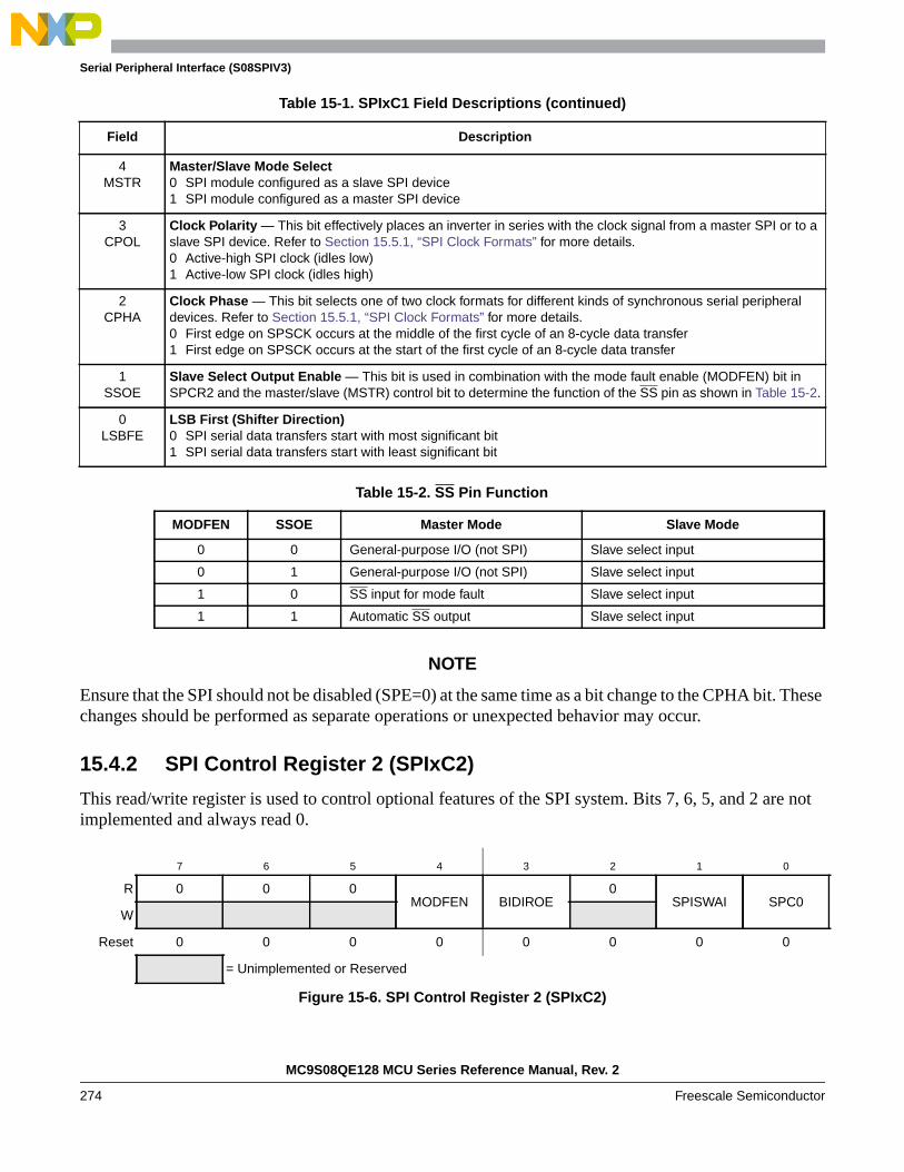
Serial Peripheral Interface (S08SPIV3)
NOTE
Ensure that the SPI should not be disabled (SPE=0) at the same time as a bit change to the CPHA bit. Thesechanges should be performed as separate operations or unexpected behavior may occur.
15.4.2 SPI Control Register 2 (SPIxC2)
This read/write register is used to control optional features of the SPI system. Bits 7, 6, 5, and 2 are notimplemented and always read 0.
4MSTR
Master/Slave Mode Select0 SPI module configured as a slave SPI device1 SPI module configured as a master SPI device
3CPOL
Clock Polarity — This bit effectively places an inverter in series with the clock signal from a master SPI or to aslave SPI device. Refer to Section 15.5.1, “SPI Clock Formats” for more details.0 Active-high SPI clock (idles low)1 Active-low SPI clock (idles high)
2CPHA
Clock Phase — This bit selects one of two clock formats for different kinds of synchronous serial peripheraldevices. Refer to Section 15.5.1, “SPI Clock Formats” for more details.0 First edge on SPSCK occurs at the middle of the first cycle of an 8-cycle data transfer1 First edge on SPSCK occurs at the start of the first cycle of an 8-cycle data transfer
1SSOE
Slave Select Output Enable — This bit is used in combination with the mode fault enable (MODFEN) bit inSPCR2 and the master/slave (MSTR) control bit to determine the function of the SS pin as shown in Table 15-2.
0LSBFE
LSB First (Shifter Direction)0 SPI serial data transfers start with most significant bit1 SPI serial data transfers start with least significant bit
Table 15-2. SS Pin Function
MODFEN SSOE Master Mode Slave Mode
0 0 General-purpose I/O (not SPI) Slave select input
0 1 General-purpose I/O (not SPI) Slave select input
1 0 SS input for mode fault Slave select input
1 1 Automatic SS output Slave select input
7 6 5 4 3 2 1 0
R 0 0 0MODFEN BIDIROE
0SPISWAI SPC0
W
Reset 0 0 0 0 0 0 0 0
= Unimplemented or Reserved
Figure 15-6. SPI Control Register 2 (SPIxC2)
Table 15-1. SPIxC1 Field Descriptions (continued)
Field Description
MC9S08QE128 MCU Series Reference Manual, Rev. 2
274 Freescale Semiconductor

Serial Peripheral Interface (S08SPIV3)
15.4.3 SPI Baud Rate Register (SPIxBR)
This register is used to set the prescaler and bit rate divisor for an SPI master. This register may be read orwritten at any time.
Table 15-3. SPIxC2 Register Field Descriptions
Field Description
4MODFEN
Master Mode-Fault Function Enable — When the SPI is configured for slave mode, this bit has no meaning oreffect. (The SS pin is the slave select input.) In master mode, this bit determines how the SS pin is used (referto Table 15-2 for more details).0 Mode fault function disabled, master SS pin reverts to general-purpose I/O not controlled by SPI1 Mode fault function enabled, master SS pin acts as the mode fault input or the slave select output
3BIDIROE
Bidirectional Mode Output Enable — When bidirectional mode is enabled by SPI pin control 0 (SPC0) = 1,BIDIROE determines whether the SPI data output driver is enabled to the single bidirectional SPI I/O pin.Depending on whether the SPI is configured as a master or a slave, it uses either the MOSI (MOMI) or MISO(SISO) pin, respectively, as the single SPI data I/O pin. When SPC0 = 0, BIDIROE has no meaning or effect.0 Output driver disabled so SPI data I/O pin acts as an input1 SPI I/O pin enabled as an output
1SPISWAI
SPI Stop in Wait Mode0 SPI clocks continue to operate in wait mode1 SPI clocks stop when the MCU enters wait mode
0SPC0
SPI Pin Control 0 — The SPC0 bit chooses single-wire bidirectional mode. If MSTR = 0 (slave mode), the SPIuses the MISO (SISO) pin for bidirectional SPI data transfers. If MSTR = 1 (master mode), the SPI uses theMOSI (MOMI) pin for bidirectional SPI data transfers. When SPC0 = 1, BIDIROE is used to enable or disable theoutput driver for the single bidirectional SPI I/O pin.0 SPI uses separate pins for data input and data output1 SPI configured for single-wire bidirectional operation
7 6 5 4 3 2 1 0
R 0SPPR2 SPPR1 SPPR0
0SPR2 SPR1 SPR0
W
Reset 0 0 0 0 0 0 0 0
= Unimplemented or Reserved
Figure 15-7. SPI Baud Rate Register (SPIxBR)
Table 15-4. SPIxBR Register Field Descriptions
Field Description
6:4SPPR[2:0]
SPI Baud Rate Prescale Divisor — This 3-bit field selects one of eight divisors for the SPI baud rate prescaleras shown in Table 15-5. The input to this prescaler is the bus rate clock (BUSCLK). The output of this prescalerdrives the input of the SPI baud rate divider (see Figure 15-4).
2:0SPR[2:0]
SPI Baud Rate Divisor — This 3-bit field selects one of eight divisors for the SPI baud rate divider as shown inTable 15-6. The input to this divider comes from the SPI baud rate prescaler (see Figure 15-4). The output of thisdivider is the SPI bit rate clock for master mode.
MC9S08QE128 MCU Series Reference Manual, Rev. 2
Freescale Semiconductor 275

Serial Peripheral Interface (S08SPIV3)
15.4.4 SPI Status Register (SPIxS)
This register has three read-only status bits. Bits 6, 3, 2, 1, and 0 are not implemented and always read 0.Writes have no meaning or effect.
Table 15-5. SPI Baud Rate Prescaler Divisor
SPPR2:SPPR1:SPPR0 Prescaler Divisor
0:0:0 1
0:0:1 2
0:1:0 3
0:1:1 4
1:0:0 5
1:0:1 6
1:1:0 7
1:1:1 8
Table 15-6. SPI Baud Rate Divisor
SPR2:SPR1:SPR0 Rate Divisor
0:0:0 2
0:0:1 4
0:1:0 8
0:1:1 16
1:0:0 32
1:0:1 64
1:1:0 128
1:1:1 256
7 6 5 4 3 2 1 0
R SPRF 0 SPTEF MODF 0 0 0 0
W
Reset 0 0 1 0 0 0 0 0
= Unimplemented or Reserved
Figure 15-8. SPI Status Register (SPIxS)
MC9S08QE128 MCU Series Reference Manual, Rev. 2
276 Freescale Semiconductor

Serial Peripheral Interface (S08SPIV3)
15.4.5 SPI Data Register (SPIxD)
Reads of this register return the data read from the receive data buffer. Writes to this register write data tothe transmit data buffer. When the SPI is configured as a master, writing data to the transmit data bufferinitiates an SPI transfer.
Data should not be written to the transmit data buffer unless the SPI transmit buffer empty flag (SPTEF)is set, indicating there is room in the transmit buffer to queue a new transmit byte.
Data may be read from SPIxD any time after SPRF is set and before another transfer is finished. Failureto read the data out of the receive data buffer before a new transfer ends causes a receive overrun conditionand the data from the new transfer is lost.
Table 15-7. SPIxS Register Field Descriptions
Field Description
7SPRF
SPI Read Buffer Full Flag — SPRF is set at the completion of an SPI transfer to indicate that received data maybe read from the SPI data register (SPIxD). SPRF is cleared by reading SPRF while it is set, then reading theSPI data register.0 No data available in the receive data buffer1 Data available in the receive data buffer
5SPTEF
SPI Transmit Buffer Empty Flag — This bit is set when there is room in the transmit data buffer. It is cleared byreading SPIxS with SPTEF set, followed by writing a data value to the transmit buffer at SPIxD. SPIxS must beread with SPTEF = 1 before writing data to SPIxD or the SPIxD write will be ignored. SPTEF generates anSPTEF CPU interrupt request if the SPTIE bit in the SPIxC1 is also set. SPTEF is automatically set when a databyte transfers from the transmit buffer into the transmit shift register. For an idle SPI (no data in the transmit bufferor the shift register and no transfer in progress), data written to SPIxD is transferred to the shifter almostimmediately so SPTEF is set within two bus cycles allowing a second 8-bit data value to be queued into thetransmit buffer. After completion of the transfer of the value in the shift register, the queued value from thetransmit buffer will automatically move to the shifter and SPTEF will be set to indicate there is room for new datain the transmit buffer. If no new data is waiting in the transmit buffer, SPTEF simply remains set and no datamoves from the buffer to the shifter.0 SPI transmit buffer not empty1 SPI transmit buffer empty
4MODF
Master Mode Fault Flag — MODF is set if the SPI is configured as a master and the slave select input goeslow, indicating some other SPI device is also configured as a master. The SS pin acts as a mode fault error inputonly when MSTR = 1, MODFEN = 1, and SSOE = 0; otherwise, MODF will never be set. MODF is cleared byreading MODF while it is 1, then writing to SPI control register 1 (SPIxC1).0 No mode fault error1 Mode fault error detected
7 6 5 4 3 2 1 0
RBit 7 6 5 4 3 2 1 Bit 0
W
Reset 0 0 0 0 0 0 0 0
Figure 15-9. SPI Data Register (SPIxD)
MC9S08QE128 MCU Series Reference Manual, Rev. 2
Freescale Semiconductor 277

Serial Peripheral Interface (S08SPIV3)
15.5 Functional DescriptionAn SPI transfer is initiated by checking for the SPI transmit buffer empty flag (SPTEF = 1) and thenwriting a byte of data to the SPI data register (SPIxD) in the master SPI device. When the SPI shift registeris available, this byte of data is moved from the transmit data buffer to the shifter, SPTEF is set to indicatethere is room in the buffer to queue another transmit character if desired, and the SPI serial transfer starts.
During the SPI transfer, data is sampled (read) on the MISO pin at one SPSCK edge and shifted, changingthe bit value on the MOSI pin, one-half SPSCK cycle later. After eight SPSCK cycles, the data that was inthe shift register of the master has been shifted out the MOSI pin to the slave while eight bits of data wereshifted in the MISO pin into the master’s shift register. At the end of this transfer, the received data byte ismoved from the shifter into the receive data buffer and SPRF is set to indicate the data can be read byreading SPIxD. If another byte of data is waiting in the transmit buffer at the end of a transfer, it is movedinto the shifter, SPTEF is set, and a new transfer is started.
Normally, SPI data is transferred most significant bit (MSB) first. If the least significant bit first enable(LSBFE) bit is set, SPI data is shifted LSB first.
When the SPI is configured as a slave, its SS pin must be driven low before a transfer starts and SS muststay low throughout the transfer. If a clock format where CPHA = 0 is selected, SS must be driven to alogic 1 between successive transfers. If CPHA = 1, SS may remain low between successive transfers. SeeSection 15.5.1, “SPI Clock Formats” for more details.
Because the transmitter and receiver are double buffered, a second byte, in addition to the byte currentlybeing shifted out, can be queued into the transmit data buffer, and a previously received character can bein the receive data buffer while a new character is being shifted in. The SPTEF flag indicates when thetransmit buffer has room for a new character. The SPRF flag indicates when a received character isavailable in the receive data buffer. The received character must be read out of the receive buffer (readSPIxD) before the next transfer is finished or a receive overrun error results.
In the case of a receive overrun, the new data is lost because the receive buffer still held the previouscharacter and was not ready to accept the new data. There is no indication for such an overrun conditionso the application system designer must ensure that previous data has been read from the receive bufferbefore a new transfer is initiated.
15.5.1 SPI Clock Formats
To accommodate a wide variety of synchronous serial peripherals from different manufacturers, the SPIsystem has a clock polarity (CPOL) bit and a clock phase (CPHA) control bit to select one of four clockformats for data transfers. CPOL selectively inserts an inverter in series with the clock. CPHA choosesbetween two different clock phase relationships between the clock and data.
Figure 15-10 shows the clock formats when CPHA = 1. At the top of the figure, the eight bit times areshown for reference with bit 1 starting at the first SPSCK edge and bit 8 ending one-half SPSCK cycle afterthe sixteenth SPSCK edge. The MSB first and LSB first lines show the order of SPI data bits dependingon the setting in LSBFE. Both variations of SPSCK polarity are shown, but only one of these waveformsapplies for a specific transfer, depending on the value in CPOL. The SAMPLE IN waveform applies to theMOSI input of a slave or the MISO input of a master. The MOSI waveform applies to the MOSI output
MC9S08QE128 MCU Series Reference Manual, Rev. 2
278 Freescale Semiconductor

Serial Peripheral Interface (S08SPIV3)
pin from a master and the MISO waveform applies to the MISO output from a slave. The SS OUTwaveform applies to the slave select output from a master (provided MODFEN and SSOE = 1). The masterSS output goes to active low one-half SPSCK cycle before the start of the transfer and goes back high atthe end of the eighth bit time of the transfer. The SS IN waveform applies to the slave select input of aslave.
Figure 15-10. SPI Clock Formats (CPHA = 1)
When CPHA = 1, the slave begins to drive its MISO output when SS goes to active low, but the data is notdefined until the first SPSCK edge. The first SPSCK edge shifts the first bit of data from the shifter ontothe MOSI output of the master and the MISO output of the slave. The next SPSCK edge causes both themaster and the slave to sample the data bit values on their MISO and MOSI inputs, respectively. At thethird SPSCK edge, the SPI shifter shifts one bit position which shifts in the bit value that was just sampled,and shifts the second data bit value out the other end of the shifter to the MOSI and MISO outputs of themaster and slave, respectively. When CHPA = 1, the slave’s SS input is not required to go to its inactivehigh level between transfers.
Figure 15-11 shows the clock formats when CPHA = 0. At the top of the figure, the eight bit times areshown for reference with bit 1 starting as the slave is selected (SS IN goes low), and bit 8 ends at the lastSPSCK edge. The MSB first and LSB first lines show the order of SPI data bits depending on the setting
BIT TIME #(REFERENCE)
MSB FIRSTLSB FIRST
SPSCK(CPOL = 0)
SPSCK(CPOL = 1)
SAMPLE IN(MISO OR MOSI)
MOSI(MASTER OUT)
MISO(SLAVE OUT)
SS OUT(MASTER)
SS IN(SLAVE)
BIT 7BIT 0
BIT 6BIT 1
BIT 2BIT 5
BIT 1BIT 6
BIT 0BIT 7
1 2 6 7 8
...
...
...
MC9S08QE128 MCU Series Reference Manual, Rev. 2
Freescale Semiconductor 279
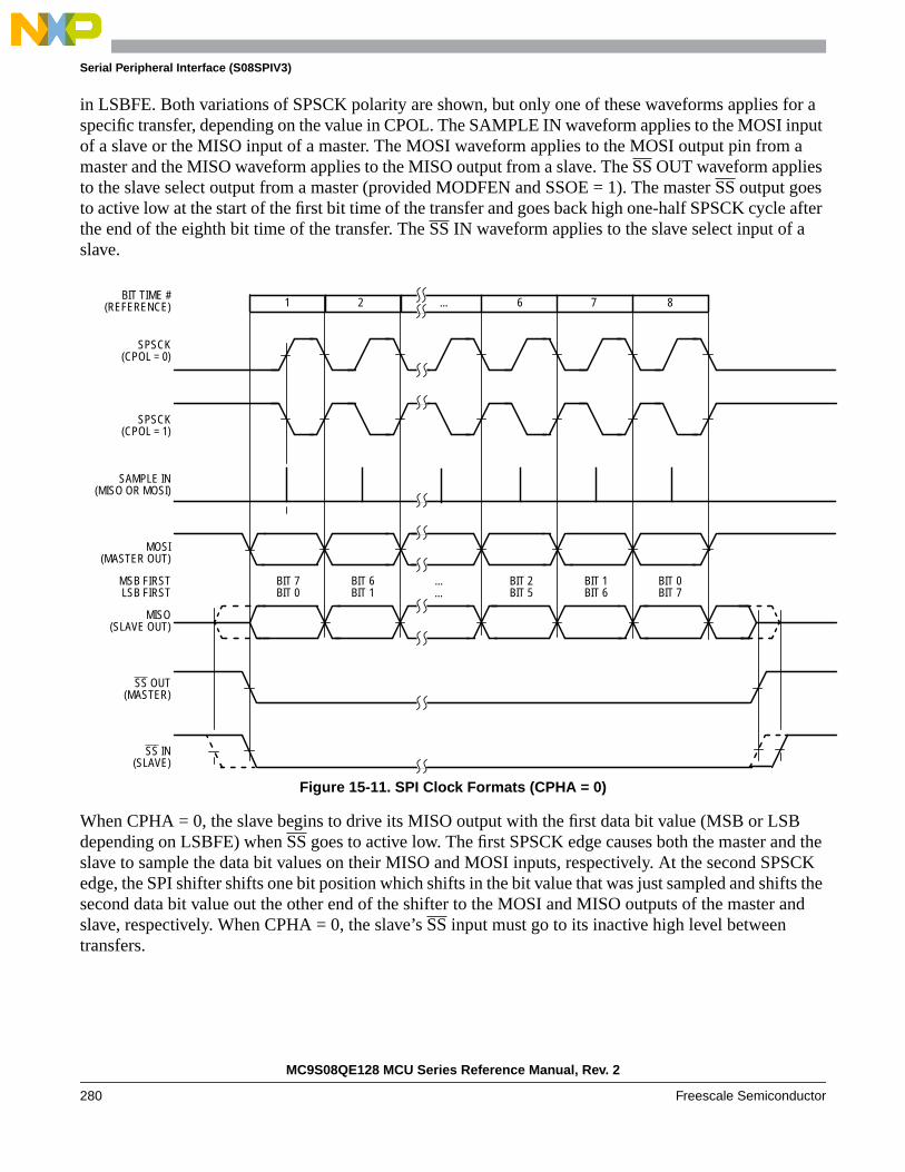
Serial Peripheral Interface (S08SPIV3)
in LSBFE. Both variations of SPSCK polarity are shown, but only one of these waveforms applies for aspecific transfer, depending on the value in CPOL. The SAMPLE IN waveform applies to the MOSI inputof a slave or the MISO input of a master. The MOSI waveform applies to the MOSI output pin from amaster and the MISO waveform applies to the MISO output from a slave. The SS OUT waveform appliesto the slave select output from a master (provided MODFEN and SSOE = 1). The master SS output goesto active low at the start of the first bit time of the transfer and goes back high one-half SPSCK cycle afterthe end of the eighth bit time of the transfer. The SS IN waveform applies to the slave select input of aslave.
Figure 15-11. SPI Clock Formats (CPHA = 0)
When CPHA = 0, the slave begins to drive its MISO output with the first data bit value (MSB or LSBdepending on LSBFE) when SS goes to active low. The first SPSCK edge causes both the master and theslave to sample the data bit values on their MISO and MOSI inputs, respectively. At the second SPSCKedge, the SPI shifter shifts one bit position which shifts in the bit value that was just sampled and shifts thesecond data bit value out the other end of the shifter to the MOSI and MISO outputs of the master andslave, respectively. When CPHA = 0, the slave’s SS input must go to its inactive high level betweentransfers.
BIT TIME #(REFERENCE)
MSB FIRSTLSB FIRST
SPSCK(CPOL = 0)
SPSCK(CPOL = 1)
SAMPLE IN(MISO OR MOSI)
MOSI(MASTER OUT)
MISO(SLAVE OUT)
SS OUT(MASTER)
SS IN(SLAVE)
BIT 7BIT 0
BIT 6BIT 1
BIT 2BIT 5
BIT 1BIT 6
BIT 0BIT 7
1 2 6 7 8...
...
...
MC9S08QE128 MCU Series Reference Manual, Rev. 2
280 Freescale Semiconductor

Serial Peripheral Interface (S08SPIV3)
15.5.2 SPI Interrupts
There are three flag bits, two interrupt mask bits, and one interrupt vector associated with the SPI system.The SPI interrupt enable mask (SPIE) enables interrupts from the SPI receiver full flag (SPRF) and modefault flag (MODF). The SPI transmit interrupt enable mask (SPTIE) enables interrupts from the SPItransmit buffer empty flag (SPTEF). When one of the flag bits is set, and the associated interrupt mask bitis set, a hardware interrupt request is sent to the CPU. If the interrupt mask bits are cleared, software canpoll the associated flag bits instead of using interrupts. The SPI interrupt service routine (ISR) shouldcheck the flag bits to determine what event caused the interrupt. The service routine should also clear theflag bit(s) before returning from the ISR (usually near the beginning of the ISR).
15.5.3 Mode Fault Detection
A mode fault occurs and the mode fault flag (MODF) becomes set when a master SPI device detects anerror on the SS pin (provided the SS pin is configured as the mode fault input signal). The SS pin isconfigured to be the mode fault input signal when MSTR = 1, mode fault enable is set (MODFEN = 1),and slave select output enable is clear (SSOE = 0).
The mode fault detection feature can be used in a system where more than one SPI device might becomea master at the same time. The error is detected when a master’s SS pin is low, indicating that some otherSPI device is trying to address this master as if it were a slave. This could indicate a harmful output driverconflict, so the mode fault logic is designed to disable all SPI output drivers when such an error is detected.
When a mode fault is detected, MODF is set and MSTR is cleared to change the SPI configuration backto slave mode. The output drivers on the SPSCK, MOSI, and MISO (if not bidirectional mode) aredisabled.
MODF is cleared by reading it while it is set, then writing to the SPI control register 1 (SPIxC1). Usersoftware should verify the error condition has been corrected before changing the SPI back to mastermode.
MC9S08QE128 MCU Series Reference Manual, Rev. 2
Freescale Semiconductor 281

Serial Peripheral Interface (S08SPIV3)
MC9S08QE128 MCU Series Reference Manual, Rev. 2
282 Freescale Semiconductor

Chapter 16Timer/Pulse-Width Modulator (S08TPMV3)
16.1 IntroductionFigure 16-1 shows the MC9S08QE128 Series block diagram with the TPM highlighted.
16.1.1 ACMP/TPM Configuration Information
The ACMP modules can be configured to connect the output of the analog comparator to a TPM inputcapture channel 0 by setting the corresponding SOPT2[ACICx] bit. With ACICx set, the TPMxCH0 pin isnot available externally regardless of the configuration of the TPMx module.
The ACMP1 output can be connected to TPM1CH0; The ACMP2 output can be connected to TPM2CH0.
16.1.2 TPM Clock Gating
The bus clock to TPM1, TPM2, and TPM3 can be gated on and off using the SCGC1[TPMx] bits. Thesebits are set after any reset, which enables the bus clock to this module. To conserve power, these bits canbe cleared to disable the clock to any of these modules when not in use. See Section 5.7, “Peripheral ClockGating,” for details.
16.1.3 Interrupt Vector
See Section 4.2, “Reset and Interrupt Vector Assignments,” for the TPM interrupt vector assignments.
MC9S08QE128 MCU Series Reference Manual, Rev. 2
Freescale Semiconductor 283
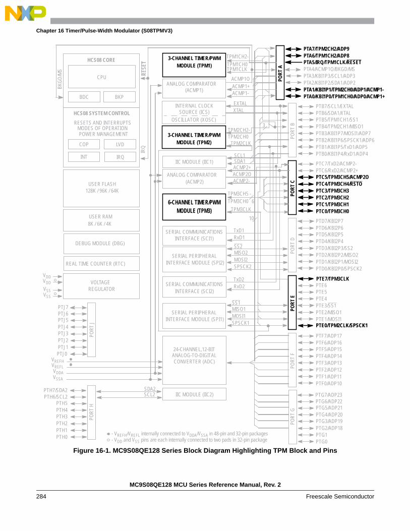
Chapter 16 Timer/Pulse-Width Modulator (S08TPMV3)
-+-
Figure 16-1. MC9S08QE128 Series Block Diagram Highlighting TPM Block and Pins
TPM2CH2-TPM2CH0
TPM1CH0
TPM1CH2-
ANALOG COMPARATOR(ACMP1)
ACMP1O
ACMP1-ACMP1+
VSS
VDD
IIC MODULE (IIC1)
SERIAL PERIPHERAL INTERFACE MODULE (SPI1)
USER FLASH
USER RAM
128K / 96K / 64K
HCS08 CORE
CPU
BDC
6-CHANNEL TIMER/PWMMODULE (TPM3)
HCS08 SYSTEM CONTROL
RESETS AND INTERRUPTSMODES OF OPERATIONPOWER MANAGEMENT
VOLTAGEREGULATOR
COP
IRQ
LVD
OSCILLATOR (XOSC)
RES
ET
VREFL
VREFH
8K / 6K / 4K
BKG
D/M
S
INTERFACE (SCI1)SERIAL COMMUNICATIONS
MISO1SS1
SPSCK1
3-CHANNEL TIMER/PWMMODULE (TPM2)
REAL TIME COUNTER (RTC)
DEBUG MODULE (DBG)
IRQ
PTA3/KBI1P3/SCL1/ADP3PTA4/ACMP1O/BKGD/MSPTA5/IRQ/TPM1CLK/RESET
PTA2/KBI1P2/SDA1/ADP2PTA1/KBI1P1/TPM2CH0/ADP1/ACMP1PTA0/KBI1P0/TPM1CH0/ADP0/ACMP1
PORT
A
PTA6/TPM1CH2/ADP8PTA7/TPM2CH2/ADP9
MOSI1
PTB3/KBI1P7/MOSI1/ADP7PTB4/TPM2CH1/MISO1PTB5/TPM1CH1/SS1
PTB2/KBI1P6/SPSCK1/ADP6PTB1/KBI1P5/TxD1/ADP5PTB0/KBI1P4/RxD1/ADP4
PORT
B
PTB6/SDA1/XTALPTB7/SCL1/EXTAL
PTC3/TPM3CH3PTC4/TPM3CH4/RSTOPTC5/TPM3CH5/ACMP2O
PTC2/TPM3CH2PTC1/TPM3CH1PTC0/TPM3CH0
PORT
C
PTC6/RxD2/ACMP2+PTC7/TxD2/ACMP2-
PTD3/KBI2P3/SS2PTD4/KBI2P4PTD5/KBI2P5
PTD2/KBI2P2/MISO2PTD1/KBI2P1/MOSI2PTD0/KBI2P0/SPSCK2
PORT
D
PTD6/KBI2P6PTD7/KBI2P7
PTE3/SS1PTE4PTE5
PTE2/MISO1PTE1/MOSI1
TPM2CLK
PORT
EPTE6
PTE0/TPM2CLK/SPSCK1
PTF3/ADP13PTF4/ADP14PTF5/ADP15
PTF2/ADP12PTF1/ADP11PTF0/ADP10
PORT
F
PTF6/ADP16PTF7/ADP17
PTG1PTG2/ADP18PTG3/ADP19PO
RT G
PTG4/ADP20PTG5/ADP21
PTG0
VSS
VDD
VSSA
VDDA
BKP
INT
ANALOG COMPARATOR(ACMP2)
INTERFACE (SCI2)SERIAL COMMUNICATIONS
6TPM3CH5 -TPM3CH0
- VREFH/VREFL internally connected to VDDA/VSSA in 48-pin and 32-pin packages- VDD and VSS pins are each internally connected to two pads in 32-pin package
PTG6/ADP22PTG7/ADP23
SOURCE (ICS)INTERNAL CLOCK
RES
ET
PORT
JPO
RT H
PTJ1PTJ2PTJ3PTJ4PTJ5
PTJ0
PTJ6PTJ7
PTH1PTH2PTH3PTH4PTH5
PTH0
PTH6/SCL2PTH7/SDA2
IIC MODULE (IIC2)
ANALOG-TO-DIGITALCONVERTER (ADC)
24-CHANNEL,12-BIT
3-CHANNEL TIMER/PWMMODULE (TPM1)
SDA2SCL2
SERIAL PERIPHERAL INTERFACE MODULE (SPI2)
MISO2SS2
SPSCK2MOSI2
EXTALXTAL
10
SDA1SCL1
ACMP2-
ACMP2+ACMP2O
RxD1TxD1
RxD2TxD2
TPM3CLK
3
TPM1CLK
PTE7/TPM3CLK
PTE0/TPM2CLK/SPSCK1
PTA1/KBI1P1/TPM2CH0/ADP1/ACMP1
MC9S08QE128 MCU Series Reference Manual, Rev. 2
284 Freescale Semiconductor

Timer/PWM Module (S08TPMV3)
MC9S08QE128 MCU Series Reference Manual, Rev. 2
Freescale Semiconductor 285
16.1.4 Features
The TPM includes these distinctive features:
• One to eight channels:— Each channel may be input capture, output compare, or edge-aligned PWM
— Rising-Edge, falling-edge, or any-edge input capture trigger
— Set, clear, or toggle output compare action
— Selectable polarity on PWM outputs
• Module may be configured for buffered, center-aligned pulse-width-modulation (CPWM) on allchannels
• Timer clock source selectable as prescaled bus clock, fixed system clock, or an external clock pin— Prescale taps for divide-by 1, 2, 4, 8, 16, 32, 64, or 128
— Fixed system clock source are synchronized to the bus clock by an on-chip synchronizationcircuit
— External clock pin may be shared with any timer channel pin or a separated input pin
• 16-bit free-running or modulo up/down count operation
• Timer system enable
• One interrupt per channel plus terminal count interrupt
16.1.5 Modes of Operation
In general, TPM channels may be independently configured to operate in input capture, output compare,or edge-aligned PWM modes. A control bit allows the whole TPM (all channels) to switch tocenter-aligned PWM mode. When center-aligned PWM mode is selected, input capture, output compare,and edge-aligned PWM functions are not available on any channels of this TPM module.
When the microcontroller is in active BDM background or BDM foreground mode, the TPM temporarilysuspends all counting until the microcontroller returns to normal user operating mode. During stop mode,all system clocks, including the main oscillator, are stopped; therefore, the TPM is effectively disableduntil clocks resume. During wait mode, the TPM continues to operate normally. Provided the TPM doesnot need to produce a real time reference or provide the interrupt source(s) needed to wake the MCU fromwait mode, the user can save power by disabling TPM functions before entering wait mode.
• Input capture mode
When a selected edge event occurs on the associated MCU pin, the current value of the 16-bit timercounter is captured into the channel value register and an interrupt flag bit is set. Rising edges,falling edges, any edge, or no edge (disable channel) may be selected as the active edge whichtriggers the input capture.
• Output compare mode
When the value in the timer counter register matches the channel value register, an interrupt flagbit is set, and a selected output action is forced on the associated MCU pin. The output compareaction may be selected to force the pin to zero, force the pin to one, toggle the pin, or ignore thepin (used for software timing functions).

Timer/PWM Module (S08TPMV3)
MC9S08QE128 MCU Series Reference Manual, Rev. 2
286 Freescale Semiconductor
• Edge-aligned PWM mode
The value of a 16-bit modulo register plus 1 sets the period of the PWM output signal. The channelvalue register sets the duty cycle of the PWM output signal. The user may also choose the polarityof the PWM output signal. Interrupts are available at the end of the period and at the duty-cycletransition point. This type of PWM signal is called edge-aligned because the leading edges of allPWM signals are aligned with the beginning of the period, which is the same for all channels withina TPM.
• Center-aligned PWM mode
Twice the value of a 16-bit modulo register sets the period of the PWM output, and thechannel-value register sets the half-duty-cycle duration. The timer counter counts up until itreaches the modulo value and then counts down until it reaches zero. As the count matches thechannel value register while counting down, the PWM output becomes active. When the countmatches the channel value register while counting up, the PWM output becomes inactive. This typeof PWM signal is called center-aligned because the centers of the active duty cycle periods for allchannels are aligned with a count value of zero. This type of PWM is required for types of motorsused in small appliances.
This is a high-level description only. Detailed descriptions of operating modes are in later sections.
16.1.6 Block Diagram
The TPM uses one input/output (I/O) pin per channel, TPMxCHn (timer channel n) where n is the channelnumber (1-8). The TPM shares its I/O pins with general purpose I/O port pins (refer to I/O pin descriptionsin full-chip specification for the specific chip implementation).
Figure 16-2 shows the TPM structure. The central component of the TPM is the 16-bit counter that canoperate as a free-running counter or a modulo up/down counter. The TPM counter (when operating innormal up-counting mode) provides the timing reference for the input capture, output compare, andedge-aligned PWM functions. The timer counter modulo registers, TPMxMODH:TPMxMODL, controlthe modulo value of the counter (the values 0x0000 or 0xFFFF effectively make the counter free running).Software can read the counter value at any time without affecting the counting sequence. Any write toeither half of the TPMxCNT counter resets the counter, regardless of the data value written.
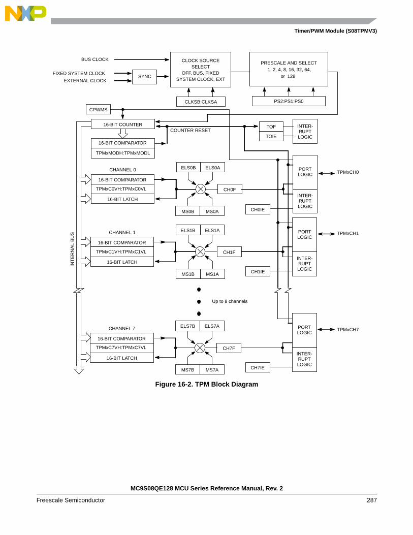
Timer/PWM Module (S08TPMV3)
MC9S08QE128 MCU Series Reference Manual, Rev. 2
Freescale Semiconductor 287
Figure 16-2. TPM Block Diagram
PRESCALE AND SELECT
16-BIT COMPARATOR
PS2:PS1:PS0
TOF
TOIE
INTER-16-BIT COUNTER
RUPTLOGIC
16-BIT COMPARATOR
16-BIT LATCH
ELS0B ELS0A PORTCHANNEL 0
CH0IE
CH0F
LOGIC
INTER-RUPTLOGIC
CPWMS
MS0B MS0A
COUNTER RESET
CLKSB:CLKSA
1, 2, 4, 8, 16, 32, 64,
BUS CLOCK
FIXED SYSTEM CLOCK
EXTERNAL CLOCKSYNC
16-BIT COMPARATOR
16-BIT LATCH
CHANNEL 1 ELS1B ELS1A
CH1IE
CH1F
INT
ER
NA
L B
US PORT
LOGIC
INTER-RUPTLOGIC
MS1B MS1A
16-BIT COMPARATOR
16-BIT LATCH
CHANNEL 7 ELS7B ELS7A
CH7IE
CH7F
PORTLOGIC
INTER-RUPTLOGIC
MS7B MS7A
Up to 8 channels
CLOCK SOURCESELECT
OFF, BUS, FIXEDSYSTEM CLOCK, EXT
or 128
TPMxMODH:TPMxMODL
TPMxC0VH:TPMxC0VL
TPMxC1VH:TPMxC1VL
TPMxCH0
TPMxCH1
TPMxC7VH:TPMxC7VL
TPMxCH7

Timer/PWM Module (S08TPMV3)
MC9S08QE128 MCU Series Reference Manual, Rev. 2
288 Freescale Semiconductor
The TPM channels are programmable independently as input capture, output compare, or edge-alignedPWM channels. Alternately, the TPM can be configured to produce CPWM outputs on all channels. Whenthe TPM is configured for CPWMs, the counter operates as an up/down counter; input capture, outputcompare, and EPWM functions are not practical.
If a channel is configured as input capture, an internal pullup device may be enabled for that channel. Thedetails of how a module interacts with pin controls depends upon the chip implementation because the I/Opins and associated general purpose I/O controls are not part of the module. Refer to the discussion of theI/O port logic in a full-chip specification.
Because center-aligned PWMs are usually used to drive 3-phase AC-induction motors and brushless DCmotors, they are typically used in sets of three or six channels.
16.2 Signal DescriptionTable 16-1 shows the user-accessible signals for the TPM. The number of channels may be varied fromone to eight. When an external clock is included, it can be shared with the same pin as any TPM channel;however, it could be connected to a separate input pin. Refer to the I/O pin descriptions in full-chipspecification for the specific chip implementation.
Refer to documentation for the full-chip for details about reset states, port connections, and whether thereis any pullup device on these pins.
TPM channel pins can be associated with general purpose I/O pins and have passive pullup devices whichcan be enabled with a control bit when the TPM or general purpose I/O controls have configured theassociated pin as an input. When no TPM function is enabled to use a corresponding pin, the pin revertsto being controlled by general purpose I/O controls, including the port-data and data-direction registers.Immediately after reset, no TPM functions are enabled, so all associated pins revert to general purpose I/Ocontrol.
16.2.1 Detailed Signal Descriptions
This section describes each user-accessible pin signal in detail. Although Table 16-1 grouped all channelpins together, any TPM pin can be shared with the external clock source signal. Since I/O pin logic is notpart of the TPM, refer to full-chip documentation for a specific derivative for more details about theinteraction of TPM pin functions and general purpose I/O controls including port data, data direction, andpullup controls.
Table 16-1. Signal Properties
Name Function
EXTCLK1
1 When preset, this signal can share any channel pin; however depending upon full-chipimplementation, this signal could be connected to a separate external pin.
External clock source which may be selected to drive the TPM counter.
TPMxCHn2
2 n=channel number (1 to 8)
I/O pin associated with TPM channel n

Timer/PWM Module (S08TPMV3)
MC9S08QE128 MCU Series Reference Manual, Rev. 2
Freescale Semiconductor 289
16.2.1.1 EXTCLK — External Clock Source
Control bits in the timer status and control register allow the user to select nothing (timer disable), thebus-rate clock (the normal default source), a crystal-related clock, or an external clock as the clock whichdrives the TPM prescaler and subsequently the 16-bit TPM counter. The external clock source issynchronized in the TPM. The bus clock clocks the synchronizer; the frequency of the external source mustbe no more than one-fourth the frequency of the bus-rate clock, to meet Nyquist criteria and allowing forjitter.
The external clock signal shares the same pin as a channel I/O pin, so the channel pin will not be usablefor channel I/O function when selected as the external clock source. It is the user’s responsibility to avoidsuch settings. If this pin is used as an external clock source (CLKSB:CLKSA = 1:1), the channel can stillbe used in output compare mode as a software timer (ELSnB:ELSnA = 0:0).
16.2.1.2 TPMxCHn — TPM Channel n I/O Pin(s)
Each TPM channel is associated with an I/O pin on the MCU. The function of this pin depends on thechannel configuration. The TPM pins share with general purpose I/O pins, where each pin has a port dataregister bit, and a data direction control bit, and the port has optional passive pullups which may be enabledwhenever a port pin is acting as an input.
The TPM channel does not control the I/O pin when (ELSnB:ELSnA = 0:0) or when (CLKSB:CLKSA =0:0) so it normally reverts to general purpose I/O control. When CPWMS = 1 (and ELSnB:ELSnA not =0:0), all channels within the TPM are configured for center-aligned PWM and the TPMxCHn pins are allcontrolled by the TPM system. When CPWMS=0, the MSnB:MSnA control bits determine whether thechannel is configured for input capture, output compare, or edge-aligned PWM.
When a channel is configured for input capture (CPWMS=0, MSnB:MSnA = 0:0 and ELSnB:ELSnA not= 0:0), the TPMxCHn pin is forced to act as an edge-sensitive input to the TPM. ELSnB:ELSnA controlbits determine what polarity edge or edges will trigger input-capture events. A synchronizer based on thebus clock is used to synchronize input edges to the bus clock. This implies the minimum pulse width—thatcan be reliably detected—on an input capture pin is four bus clock periods (with ideal clock pulses as nearas two bus clocks can be detected). TPM uses this pin as an input capture input to override the port dataand data direction controls for the same pin.
When a channel is configured for output compare (CPWMS=0, MSnB:MSnA = 0:1 and ELSnB:ELSnAnot = 0:0), the associated data direction control is overridden, the TPMxCHn pin is considered an outputcontrolled by the TPM, and the ELSnB:ELSnA control bits determine how the pin is controlled. Theremaining three combinations of ELSnB:ELSnA determine whether the TPMxCHn pin is toggled, cleared,or set each time the 16-bit channel value register matches the timer counter.
When the output compare toggle mode is initially selected, the previous value on the pin is driven out untilthe next output compare event—then the pin is toggled.

Timer/PWM Module (S08TPMV3)
MC9S08QE128 MCU Series Reference Manual, Rev. 2
290 Freescale Semiconductor
When a channel is configured for edge-aligned PWM (CPWMS=0, MSnB=1 and ELSnB:ELSnA not =0:0), the data direction is overridden, the TPMxCHn pin is forced to be an output controlled by the TPM,and ELSnA controls the polarity of the PWM output signal on the pin. When ELSnB:ELSnA=1:0, theTPMxCHn pin is forced high at the start of each new period (TPMxCNT=0x0000), and the pin is forcedlow when the channel value register matches the timer counter. When ELSnA=1, the TPMxCHn pin isforced low at the start of each new period (TPMxCNT=0x0000), and the pin is forced high when thechannel value register matches the timer counter.
Figure 16-3. High-True Pulse of an Edge-Aligned PWM
Figure 16-4. Low-True Pulse of an Edge-Aligned PWM
CHnF BIT
TOF BIT
0... 1 2 3 4 5 6 7 8 0 1 2 ...
TPMxMODH:TPMxMODL = 0x0008TPMxMODH:TPMxMODL = 0x0005
TPMxCNTH:TPMxCNTL
TPMxCHn
CHnF BIT
TOF BIT
0... 1 2 3 4 5 6 7 8 0 1 2 ...
TPMxMODH:TPMxMODL = 0x0008TPMxMODH:TPMxMODL = 0x0005
TPMxCNTH:TPMxCNTL
TPMxCHn

Timer/PWM Module (S08TPMV3)
MC9S08QE128 MCU Series Reference Manual, Rev. 2
Freescale Semiconductor 291
When the TPM is configured for center-aligned PWM (and ELSnB:ELSnA not = 0:0), the data directionfor all channels in this TPM are overridden, the TPMxCHn pins are forced to be outputs controlled by theTPM, and the ELSnA bits control the polarity of each TPMxCHn output. If ELSnB:ELSnA=1:0, thecorresponding TPMxCHn pin is cleared when the timer counter is counting up, and the channel valueregister matches the timer counter; the TPMxCHn pin is set when the timer counter is counting down, andthe channel value register matches the timer counter. If ELSnA=1, the corresponding TPMxCHn pin is setwhen the timer counter is counting up and the channel value register matches the timer counter; theTPMxCHn pin is cleared when the timer counter is counting down and the channel value register matchesthe timer counter.
Figure 16-5. High-True Pulse of a Center-Aligned PWM
Figure 16-6. Low-True Pulse of a Center-Aligned PWM
CHnF BIT
TOF BIT
... 7 8 7 6 5 4 3 2 1 0 1 2 3 4 5 6 7 8 7 6 5 ...
TPMxMODH:TPMxMODL = 0x0008TPMxMODH:TPMxMODL = 0x0005
TPMxCNTH:TPMxCNTL
TPMxCHn
CHnF BIT
TOF BIT
... 7 8 7 6 5 4 3 2 1 0 1 2 3 4 5 6 7 8 7 6 5 ...
TPMxMODH:TPMxMODL = 0x0008TPMxMODH:TPMxMODL = 0x0005
TPMxCNTH:TPMxCNTL
TPMxCHn

Timer/PWM Module (S08TPMV3)
MC9S08QE128 MCU Series Reference Manual, Rev. 2
292 Freescale Semiconductor
16.3 Register DefinitionThis section consists of register descriptions in address order.
16.3.1 TPM Status and Control Register (TPMxSC)
TPMxSC contains the overflow status flag and control bits used to configure the interrupt enable, TPMconfiguration, clock source, and prescale factor. These controls relate to all channels within this timermodule.
7 6 5 4 3 2 1 0
R TOFTOIE CPWMS CLKSB CLKSA PS2 PS1 PS0
W 0
Reset 0 0 0 0 0 0 0 0
Figure 16-7. TPM Status and Control Register (TPMxSC)
Table 16-2. TPMxSC Field Descriptions
Field Description
7TOF
Timer overflow flag. This read/write flag is set when the TPM counter resets to 0x0000 after reaching the modulovalue programmed in the TPM counter modulo registers. Clear TOF by reading the TPM status and controlregister when TOF is set and then writing a logic 0 to TOF. If another TPM overflow occurs before the clearingsequence is complete, the sequence is reset so TOF would remain set after the clear sequence was completedfor the earlier TOF. This is done so a TOF interrupt request cannot be lost during the clearing sequence for aprevious TOF. Reset clears TOF. Writing a logic 1 to TOF has no effect.0 TPM counter has not reached modulo value or overflow1 TPM counter has overflowed
6TOIE
Timer overflow interrupt enable. This read/write bit enables TPM overflow interrupts. If TOIE is set, an interrupt isgenerated when TOF equals one. Reset clears TOIE.0 TOF interrupts inhibited (use for software polling)1 TOF interrupts enabled
5CPWMS
Center-aligned PWM select. When present, this read/write bit selects CPWM operating mode. By default, theTPM operates in up-counting mode for input capture, output compare, and edge-aligned PWM functions. SettingCPWMS reconfigures the TPM to operate in up/down counting mode for CPWM functions. Reset clears CPWMS.0 All channels operate as input capture, output compare, or edge-aligned PWM mode as selected by the
MSnB:MSnA control bits in each channel’s status and control register.1 All channels operate in center-aligned PWM mode.
4–3CLKS[B:A]
Clock source selects. As shown in Table 16-3, this 2-bit field is used to disable the TPM system or select one ofthree clock sources to drive the counter prescaler. The fixed system clock source is only meaningful in systemswith a PLL-based system clock. When there is no PLL, the fixed-system clock source is the same as the bus rateclock. The external source is synchronized to the bus clock by TPM module, and the fixed system clock source(when a PLL is present) is synchronized to the bus clock by an on-chip synchronization circuit. When a PLL ispresent but not enabled, the fixed-system clock source is the same as the bus-rate clock.
2–0PS[2:0]
Prescale factor select. This 3-bit field selects one of 8 division factors for the TPM clock input as shown inTable 16-4. This prescaler is located after any clock source synchronization or clock source selection so it affectsthe clock source selected to drive the TPM system. The new prescale factor will affect the clock source on thenext system clock cycle after the new value is updated into the register bits.
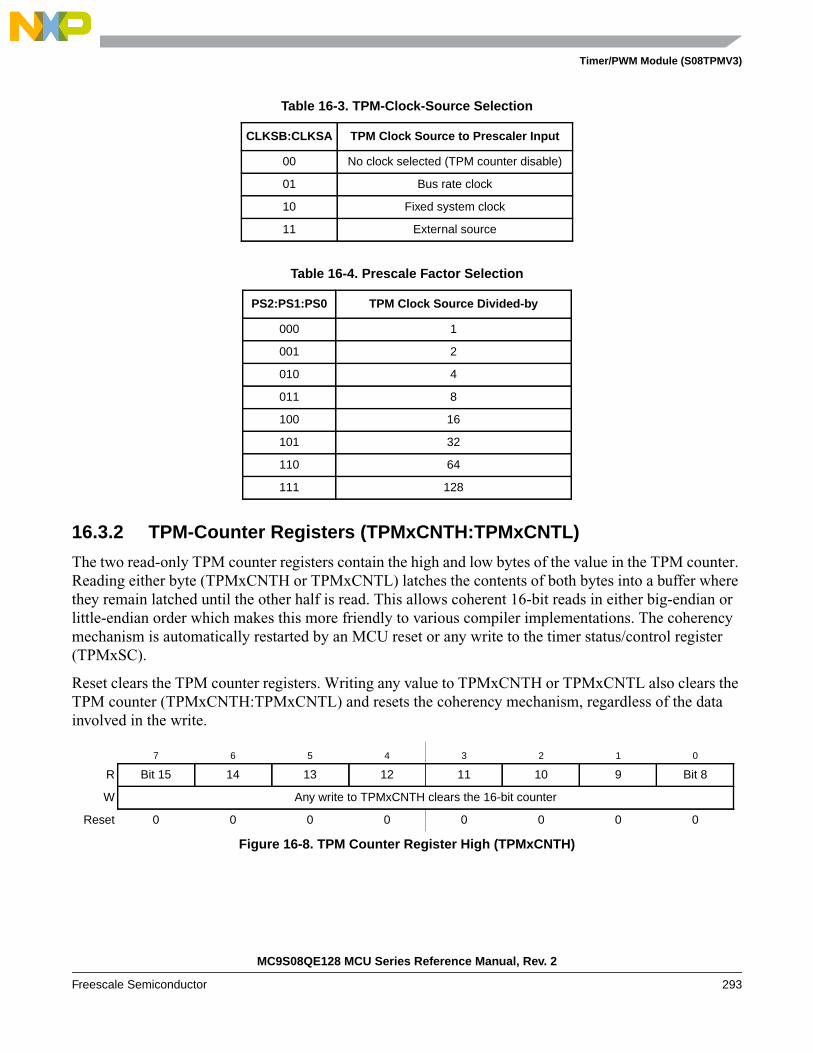
Timer/PWM Module (S08TPMV3)
MC9S08QE128 MCU Series Reference Manual, Rev. 2
Freescale Semiconductor 293
16.3.2 TPM-Counter Registers (TPMxCNTH:TPMxCNTL)
The two read-only TPM counter registers contain the high and low bytes of the value in the TPM counter.Reading either byte (TPMxCNTH or TPMxCNTL) latches the contents of both bytes into a buffer wherethey remain latched until the other half is read. This allows coherent 16-bit reads in either big-endian orlittle-endian order which makes this more friendly to various compiler implementations. The coherencymechanism is automatically restarted by an MCU reset or any write to the timer status/control register(TPMxSC).
Reset clears the TPM counter registers. Writing any value to TPMxCNTH or TPMxCNTL also clears theTPM counter (TPMxCNTH:TPMxCNTL) and resets the coherency mechanism, regardless of the datainvolved in the write.
Table 16-3. TPM-Clock-Source Selection
CLKSB:CLKSA TPM Clock Source to Prescaler Input
00 No clock selected (TPM counter disable)
01 Bus rate clock
10 Fixed system clock
11 External source
Table 16-4. Prescale Factor Selection
PS2:PS1:PS0 TPM Clock Source Divided-by
000 1
001 2
010 4
011 8
100 16
101 32
110 64
111 128
7 6 5 4 3 2 1 0
R Bit 15 14 13 12 11 10 9 Bit 8
W Any write to TPMxCNTH clears the 16-bit counter
Reset 0 0 0 0 0 0 0 0
Figure 16-8. TPM Counter Register High (TPMxCNTH)

Timer/PWM Module (S08TPMV3)
MC9S08QE128 MCU Series Reference Manual, Rev. 2
294 Freescale Semiconductor
When BDM is active, the timer counter is frozen (this is the value that will be read by user); the coherencymechanism is frozen such that the buffer latches remain in the state they were in when the BDM becameactive, even if one or both counter halves are read while BDM is active. This assures that if the user wasin the middle of reading a 16-bit register when BDM became active, it will read the appropriate value fromthe other half of the 16-bit value after returning to normal execution.
16.3.3 TPM Counter Modulo Registers (TPMxMODH:TPMxMODL)
The read/write TPM modulo registers contain the modulo value for the TPM counter. After the TPMcounter reaches the modulo value, the TPM counter resumes counting from 0x0000 at the next clock, andthe overflow flag (TOF) becomes set. Writing to TPMxMODH or TPMxMODL inhibits the TOF bit andoverflow interrupts until the other byte is written. Reset sets the TPM counter modulo registers to 0x0000which results in a free running timer counter (modulo disabled).
Writing to either byte (TPMxMODH or TPMxMODL) latches the value into a buffer and the registers areupdated with the value of their write buffer according to the value of CLKSB:CLKSA bits, so:
• If (CLKSB:CLKSA = 0:0), then the registers are updated when the second byte is written
• If (CLKSB:CLKSA not = 0:0), then the registers are updated after both bytes were written, and theTPM counter changes from (TPMxMODH:TPMxMODL - 1) to (TPMxMODH:TPMxMODL). Ifthe TPM counter is a free-running counter, the update is made when the TPM counter changes from0xFFFE to 0xFFFF
The latching mechanism may be manually reset by writing to the TPMxSC address (whether BDM isactive or not).
When BDM is active, the coherency mechanism is frozen such that the buffer latches remain in the statethey were in when the BDM became active, even if one or both halves of the modulo register are writtenwhile BDM is active. Any write to the modulo registers bypasses the buffer latches and directly writes tothe modulo register while BDM is active.
7 6 5 4 3 2 1 0
R Bit 7 6 5 4 3 2 1 Bit 0
W Any write to TPMxCNTL clears the 16-bit counter
Reset 0 0 0 0 0 0 0 0
Figure 16-9. TPM Counter Register Low (TPMxCNTL)
7 6 5 4 3 2 1 0
RBit 15 14 13 12 11 10 9 Bit 8
W
Reset 0 0 0 0 0 0 0 0
Figure 16-10. TPM Counter Modulo Register High (TPMxMODH)
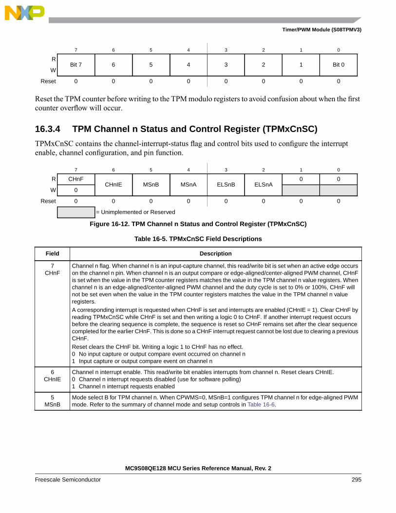
Timer/PWM Module (S08TPMV3)
MC9S08QE128 MCU Series Reference Manual, Rev. 2
Freescale Semiconductor 295
Reset the TPM counter before writing to the TPM modulo registers to avoid confusion about when the firstcounter overflow will occur.
16.3.4 TPM Channel n Status and Control Register (TPMxCnSC)
TPMxCnSC contains the channel-interrupt-status flag and control bits used to configure the interruptenable, channel configuration, and pin function.
7 6 5 4 3 2 1 0
RBit 7 6 5 4 3 2 1 Bit 0
W
Reset 0 0 0 0 0 0 0 0
7 6 5 4 3 2 1 0
R CHnFCHnIE MSnB MSnA ELSnB ELSnA
0 0
W 0
Reset 0 0 0 0 0 0 0 0
= Unimplemented or Reserved
Figure 16-12. TPM Channel n Status and Control Register (TPMxCnSC)
Table 16-5. TPMxCnSC Field Descriptions
Field Description
7CHnF
Channel n flag. When channel n is an input-capture channel, this read/write bit is set when an active edge occurson the channel n pin. When channel n is an output compare or edge-aligned/center-aligned PWM channel, CHnFis set when the value in the TPM counter registers matches the value in the TPM channel n value registers. Whenchannel n is an edge-aligned/center-aligned PWM channel and the duty cycle is set to 0% or 100%, CHnF willnot be set even when the value in the TPM counter registers matches the value in the TPM channel n valueregisters.A corresponding interrupt is requested when CHnF is set and interrupts are enabled (CHnIE = 1). Clear CHnF byreading TPMxCnSC while CHnF is set and then writing a logic 0 to CHnF. If another interrupt request occursbefore the clearing sequence is complete, the sequence is reset so CHnF remains set after the clear sequencecompleted for the earlier CHnF. This is done so a CHnF interrupt request cannot be lost due to clearing a previousCHnF.Reset clears the CHnF bit. Writing a logic 1 to CHnF has no effect.0 No input capture or output compare event occurred on channel n1 Input capture or output compare event on channel n
6CHnIE
Channel n interrupt enable. This read/write bit enables interrupts from channel n. Reset clears CHnIE.0 Channel n interrupt requests disabled (use for software polling)1 Channel n interrupt requests enabled
5MSnB
Mode select B for TPM channel n. When CPWMS=0, MSnB=1 configures TPM channel n for edge-aligned PWMmode. Refer to the summary of channel mode and setup controls in Table 16-6.
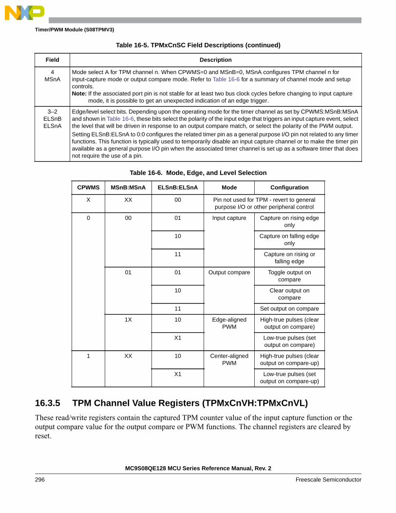
Timer/PWM Module (S08TPMV3)
MC9S08QE128 MCU Series Reference Manual, Rev. 2
296 Freescale Semiconductor
16.3.5 TPM Channel Value Registers (TPMxCnVH:TPMxCnVL)
These read/write registers contain the captured TPM counter value of the input capture function or theoutput compare value for the output compare or PWM functions. The channel registers are cleared byreset.
4MSnA
Mode select A for TPM channel n. When CPWMS=0 and MSnB=0, MSnA configures TPM channel n forinput-capture mode or output compare mode. Refer to Table 16-6 for a summary of channel mode and setupcontrols.Note: If the associated port pin is not stable for at least two bus clock cycles before changing to input capture
mode, it is possible to get an unexpected indication of an edge trigger.
3–2ELSnBELSnA
Edge/level select bits. Depending upon the operating mode for the timer channel as set by CPWMS:MSnB:MSnAand shown in Table 16-6, these bits select the polarity of the input edge that triggers an input capture event, selectthe level that will be driven in response to an output compare match, or select the polarity of the PWM output.Setting ELSnB:ELSnA to 0:0 configures the related timer pin as a general purpose I/O pin not related to any timerfunctions. This function is typically used to temporarily disable an input capture channel or to make the timer pinavailable as a general purpose I/O pin when the associated timer channel is set up as a software timer that doesnot require the use of a pin.
Table 16-6. Mode, Edge, and Level Selection
CPWMS MSnB:MSnA ELSnB:ELSnA Mode Configuration
X XX 00 Pin not used for TPM - revert to generalpurpose I/O or other peripheral control
0 00 01 Input capture Capture on rising edgeonly
10 Capture on falling edgeonly
11 Capture on rising orfalling edge
01 01 Output compare Toggle output oncompare
10 Clear output oncompare
11 Set output on compare
1X 10 Edge-alignedPWM
High-true pulses (clearoutput on compare)
X1 Low-true pulses (setoutput on compare)
1 XX 10 Center-alignedPWM
High-true pulses (clearoutput on compare-up)
X1 Low-true pulses (setoutput on compare-up)
Table 16-5. TPMxCnSC Field Descriptions (continued)
Field Description

Timer/PWM Module (S08TPMV3)
MC9S08QE128 MCU Series Reference Manual, Rev. 2
Freescale Semiconductor 297
In input capture mode, reading either byte (TPMxCnVH or TPMxCnVL) latches the contents of both bytesinto a buffer where they remain latched until the other half is read. This latching mechanism also resets(becomes unlatched) when the TPMxCnSC register is written (whether BDM mode is active or not). Anywrite to the channel registers will be ignored during the input capture mode.
When BDM is active, the coherency mechanism is frozen such that the buffer latches remain in the statethey were in when the BDM became active, even if one or both halves of the channel register are read whileBDM is active. This assures that if the user was in the middle of reading a 16-bit register when BDMbecame active, it will read the appropriate value from the other half of the 16-bit value after returning tonormal execution. The value read from the TPMxCnVH and TPMxCnVL registers in BDM mode is thevalue of these registers and not the value of their read buffer.
In output compare or PWM modes, writing to either byte (TPMxCnVH or TPMxCnVL) latches the valueinto a buffer. After both bytes are written, they are transferred as a coherent 16-bit value into thetimer-channel registers according to the value of CLKSB:CLKSA bits and the selected mode, so:
• If (CLKSB:CLKSA = 0:0), then the registers are updated when the second byte is written.
• If (CLKSB:CLKSA not = 0:0 and in output compare mode) then the registers are updated after thesecond byte is written and on the next change of the TPM counter (end of the prescaler counting).
• If (CLKSB:CLKSA not = 0:0 and in EPWM or CPWM modes), then the registers are updated afterthe both bytes were written, and the TPM counter changes from (TPMxMODH:TPMxMODL - 1)to (TPMxMODH:TPMxMODL). If the TPM counter is a free-running counter then the update ismade when the TPM counter changes from 0xFFFE to 0xFFFF.
The latching mechanism may be manually reset by writing to the TPMxCnSC register (whether BDMmode is active or not). This latching mechanism allows coherent 16-bit writes in either big-endian orlittle-endian order which is friendly to various compiler implementations.
When BDM is active, the coherency mechanism is frozen such that the buffer latches remain in the statethey were in when the BDM became active even if one or both halves of the channel register are writtenwhile BDM is active. Any write to the channel registers bypasses the buffer latches and directly write tothe channel register while BDM is active. The values written to the channel register while BDM is activeare used for PWM & output compare operation once normal execution resumes. Writes to the channel
7 6 5 4 3 2 1 0
RBit 15 14 13 12 11 10 9 Bit 8
W
Reset 0 0 0 0 0 0 0 0
Figure 16-13. TPM Channel Value Register High (TPMxCnVH)
7 6 5 4 3 2 1 0
RBit 7 6 5 4 3 2 1 Bit 0
W
Reset 0 0 0 0 0 0 0 0
Figure 16-14. TPM Channel Value Register Low (TPMxCnVL)
Timer/PWM Module (S08TPMV3)
MC9S08QE128 MCU Series Reference Manual, Rev. 2
298 Freescale Semiconductor
registers while BDM is active do not interfere with partial completion of a coherency sequence. After thecoherency mechanism has been fully exercised, the channel registers are updated using the buffered valueswritten (while BDM was not active) by the user.
16.4 Functional DescriptionAll TPM functions are associated with a central 16-bit counter which allows flexible selection of the clocksource and prescale factor. There is also a 16-bit modulo register associated with the main counter.
The CPWMS control bit chooses between center-aligned PWM operation for all channels in the TPM(CPWMS=1) or general purpose timing functions (CPWMS=0) where each channel can independently beconfigured to operate in input capture, output compare, or edge-aligned PWM mode. The CPWMS controlbit is located in the main TPM status and control register because it affects all channels within the TPMand influences the way the main counter operates. (In CPWM mode, the counter changes to an up/downmode rather than the up-counting mode used for general purpose timer functions.)
The following sections describe the main counter and each of the timer operating modes (input capture,output compare, edge-aligned PWM, and center-aligned PWM). Because details of pin operation andinterrupt activity depend upon the operating mode, these topics will be covered in the associated modeexplanation sections.
16.4.1 Counter
All timer functions are based on the main 16-bit counter (TPMxCNTH:TPMxCNTL). This sectiondiscusses selection of the clock source, end-of-count overflow, up-counting vs. up/down counting, andmanual counter reset.
16.4.1.1 Counter Clock Source
The 2-bit field, CLKSB:CLKSA, in the timer status and control register (TPMxSC) selects one of threepossible clock sources or OFF (which effectively disables the TPM). See Table 16-3. After any MCU reset,CLKSB:CLKSA=0:0 so no clock source is selected, and the TPM is in a very low power state. Thesecontrol bits may be read or written at any time and disabling the timer (writing 00 to the CLKSB:CLKSAfield) does not affect the values in the counter or other timer registers.

Timer/PWM Module (S08TPMV3)
MC9S08QE128 MCU Series Reference Manual, Rev. 2
Freescale Semiconductor 299
The bus rate clock is the main system bus clock for the MCU. This clock source requires nosynchronization because it is the clock that is used for all internal MCU activities including operation ofthe CPU and buses.
In MCUs that have no PLL or the PLL is not engaged, the fixed system clock source is the same as thebus-rate-clock source, and it does not go through a synchronizer. When a PLL is present and engaged, asynchronizer is required between the crystal divided-by two clock source and the timer counter so countertransitions will be properly aligned to bus-clock transitions. A synchronizer will be used at chip level tosynchronize the crystal-related source clock to the bus clock.
The external clock source may be connected to any TPM channel pin. This clock source always has to passthrough a synchronizer to assure that counter transitions are properly aligned to bus clock transitions. Thebus-rate clock drives the synchronizer; therefore, to meet Nyquist criteria even with jitter, the frequency ofthe external clock source must not be faster than the bus rate divided-by four. With ideal clocks the externalclock can be as fast as bus clock divided by four.
When the external clock source shares the TPM channel pin, this pin should not be used for other channeltiming functions. For example, it would be ambiguous to configure channel 0 for input capture when theTPM channel 0 pin was also being used as the timer external clock source. (It is the user’s responsibilityto avoid such settings.) The TPM channel could still be used in output compare mode for software timingfunctions (pin controls set not to affect the TPM channel pin).
16.4.1.2 Counter Overflow and Modulo Reset
An interrupt flag and enable are associated with the 16-bit main counter. The flag (TOF) is asoftware-accessible indication that the timer counter has overflowed. The enable signal selects betweensoftware polling (TOIE=0) where no hardware interrupt is generated, or interrupt-driven operation(TOIE=1) where a static hardware interrupt is generated whenever the TOF flag is equal to one.
The conditions causing TOF to become set depend on whether the TPM is configured for center-alignedPWM (CPWMS=1). In the simplest mode, there is no modulus limit and the TPM is not in CPWMS=1mode. In this case, the 16-bit timer counter counts from 0x0000 through 0xFFFF and overflows to 0x0000on the next counting clock. TOF becomes set at the transition from 0xFFFF to 0x0000. When a moduluslimit is set, TOF becomes set at the transition from the value set in the modulus register to 0x0000. Whenthe TPM is in center-aligned PWM mode (CPWMS=1), the TOF flag gets set as the counter changesdirection at the end of the count value set in the modulus register (that is, at the transition from the valueset in the modulus register to the next lower count value). This corresponds to the end of a PWM period(the 0x0000 count value corresponds to the center of a period).
Table 16-7. TPM Clock Source Selection
CLKSB:CLKSA TPM Clock Source to Prescaler Input
00 No clock selected (TPM counter disabled)
01 Bus rate clock
10 Fixed system clock
11 External source

Timer/PWM Module (S08TPMV3)
MC9S08QE128 MCU Series Reference Manual, Rev. 2
300 Freescale Semiconductor
16.4.1.3 Counting Modes
The main timer counter has two counting modes. When center-aligned PWM is selected (CPWMS=1), thecounter operates in up/down counting mode. Otherwise, the counter operates as a simple up counter. Asan up counter, the timer counter counts from 0x0000 through its terminal count and then continues with0x0000. The terminal count is 0xFFFF or a modulus value in TPMxMODH:TPMxMODL.
When center-aligned PWM operation is specified, the counter counts up from 0x0000 through its terminalcount and then down to 0x0000 where it changes back to up counting. Both 0x0000 and the terminal countvalue are normal length counts (one timer clock period long). In this mode, the timer overflow flag (TOF)becomes set at the end of the terminal-count period (as the count changes to the next lower count value).
16.4.1.4 Manual Counter Reset
The main timer counter can be manually reset at any time by writing any value to either half ofTPMxCNTH or TPMxCNTL. Resetting the counter in this manner also resets the coherency mechanismin case only half of the counter was read before resetting the count.
16.4.2 Channel Mode Selection
Provided CPWMS=0, the MSnB and MSnA control bits in the channel n status and control registersdetermine the basic mode of operation for the corresponding channel. Choices include input capture,output compare, and edge-aligned PWM.
16.4.2.1 Input Capture Mode
With the input-capture function, the TPM can capture the time at which an external event occurs. When anactive edge occurs on the pin of an input-capture channel, the TPM latches the contents of the TPM counterinto the channel-value registers (TPMxCnVH:TPMxCnVL). Rising edges, falling edges, or any edge maybe chosen as the active edge that triggers an input capture.
In input capture mode, the TPMxCnVH and TPMxCnVL registers are read only.
When either half of the 16-bit capture register is read, the other half is latched into a buffer to supportcoherent 16-bit accesses in big-endian or little-endian order. The coherency sequence can be manuallyreset by writing to the channel status/control register (TPMxCnSC).
An input capture event sets a flag bit (CHnF) which may optionally generate a CPU interrupt request.
While in BDM, the input capture function works as configured by the user. When an external event occurs,the TPM latches the contents of the TPM counter (which is frozen because of the BDM mode) into thechannel value registers and sets the flag bit.
16.4.2.2 Output Compare Mode
With the output-compare function, the TPM can generate timed pulses with programmable position,polarity, duration, and frequency. When the counter reaches the value in the channel-value registers of anoutput-compare channel, the TPM can set, clear, or toggle the channel pin.

Timer/PWM Module (S08TPMV3)
MC9S08QE128 MCU Series Reference Manual, Rev. 2
Freescale Semiconductor 301
In output compare mode, values are transferred to the corresponding timer channel registers only after both8-bit halves of a 16-bit register have been written and according to the value of CLKSB:CLKSA bits, so:
• If (CLKSB:CLKSA = 0:0), the registers are updated when the second byte is written
• If (CLKSB:CLKSA not = 0:0), the registers are updated at the next change of the TPM counter(end of the prescaler counting) after the second byte is written.
The coherency sequence can be manually reset by writing to the channel status/control register(TPMxCnSC).
An output compare event sets a flag bit (CHnF) which may optionally generate a CPU-interrupt request.
16.4.2.3 Edge-Aligned PWM Mode
This type of PWM output uses the normal up-counting mode of the timer counter (CPWMS=0) and canbe used when other channels in the same TPM are configured for input capture or output comparefunctions. The period of this PWM signal is determined by the value of the modulus register(TPMxMODH:TPMxMODL) plus 1. The duty cycle is determined by the setting in the timer channelregister (TPMxCnVH:TPMxCnVL). The polarity of this PWM signal is determined by the setting in theELSnA control bit. 0% and 100% duty cycle cases are possible.
The output compare value in the TPM channel registers determines the pulse width (duty cycle) of thePWM signal (Figure 16-15). The time between the modulus overflow and the output compare is the pulsewidth. If ELSnA=0, the counter overflow forces the PWM signal high, and the output compare forces thePWM signal low. If ELSnA=1, the counter overflow forces the PWM signal low, and the output compareforces the PWM signal high.
Figure 16-15. PWM Period and Pulse Width (ELSnA=0)
When the channel value register is set to 0x0000, the duty cycle is 0%. 100% duty cycle can be achievedby setting the timer-channel register (TPMxCnVH:TPMxCnVL) to a value greater than the modulussetting. This implies that the modulus setting must be less than 0xFFFF in order to get 100% duty cycle.
Because the TPM may be used in an 8-bit MCU, the settings in the timer channel registers are buffered toensure coherent 16-bit updates and to avoid unexpected PWM pulse widths. Writes to any of the registersTPMxCnVH and TPMxCnVL, actually write to buffer registers. In edge-aligned PWM mode, values aretransferred to the corresponding timer-channel registers according to the value of CLKSB:CLKSA bits, so:
• If (CLKSB:CLKSA = 0:0), the registers are updated when the second byte is written
• If (CLKSB:CLKSA not = 0:0), the registers are updated after the both bytes were written, and theTPM counter changes from (TPMxMODH:TPMxMODL - 1) to (TPMxMODH:TPMxMODL). If
PERIOD
PULSEWIDTH
OVERFLOW OVERFLOW OVERFLOW
OUTPUTCOMPARE
OUTPUTCOMPARE
OUTPUTCOMPARE
TPMxCHn

Timer/PWM Module (S08TPMV3)
MC9S08QE128 MCU Series Reference Manual, Rev. 2
302 Freescale Semiconductor
the TPM counter is a free-running counter then the update is made when the TPM counter changesfrom 0xFFFE to 0xFFFF.
16.4.2.4 Center-Aligned PWM Mode
This type of PWM output uses the up/down counting mode of the timer counter (CPWMS=1). The outputcompare value in TPMxCnVH:TPMxCnVL determines the pulse width (duty cycle) of the PWM signalwhile the period is determined by the value in TPMxMODH:TPMxMODL. TPMxMODH:TPMxMODLshould be kept in the range of 0x0001 to 0x7FFF because values outside this range can produce ambiguousresults. ELSnA will determine the polarity of the CPWM output.
pulse width = 2 x (TPMxCnVH:TPMxCnVL)
period = 2 x (TPMxMODH:TPMxMODL); TPMxMODH:TPMxMODL=0x0001-0x7FFF
If the channel-value register TPMxCnVH:TPMxCnVL is zero or negative (bit 15 set), the duty cycle willbe 0%. If TPMxCnVH:TPMxCnVL is a positive value (bit 15 clear) and is greater than the (non-zero)modulus setting, the duty cycle will be 100% because the duty cycle compare will never occur. Thisimplies the usable range of periods set by the modulus register is 0x0001 through 0x7FFE (0x7FFF if youdo not need to generate 100% duty cycle). This is not a significant limitation. The resulting period wouldbe much longer than required for normal applications.
TPMxMODH:TPMxMODL=0x0000 is a special case that should not be used with center-aligned PWMmode. When CPWMS=0, this case corresponds to the counter running free from 0x0000 through 0xFFFF,but when CPWMS=1 the counter needs a valid match to the modulus register somewhere other than at0x0000 in order to change directions from up-counting to down-counting.
The output compare value in the TPM channel registers (times 2) determines the pulse width (duty cycle)of the CPWM signal (Figure 16-16). If ELSnA=0, a compare occurred while counting up forces theCPWM output signal low and a compare occurred while counting down forces the output high. Thecounter counts up until it reaches the modulo setting in TPMxMODH:TPMxMODL, then counts downuntil it reaches zero. This sets the period equal to two times TPMxMODH:TPMxMODL.
Figure 16-16. CPWM Period and Pulse Width (ELSnA=0)
Center-aligned PWM outputs typically produce less noise than edge-aligned PWMs because fewer I/O pintransitions are lined up at the same system clock edge. This type of PWM is also required for some typesof motor drives.
PERIOD
PULSE WIDTH
COUNT=
COUNT= 0
COUNT=OUTPUT
COMPARE(COUNT DOWN)
OUTPUTCOMPARE
(COUNT UP)
TPMxCHn
2 x TPMxMODH:TPMxMODL
2 x TPMxCnVH:TPMxCnVL
TPMxMODH:TPMxMODLTPMxMODH:TPMxMODL

Timer/PWM Module (S08TPMV3)
MC9S08QE128 MCU Series Reference Manual, Rev. 2
Freescale Semiconductor 303
Input capture, output compare, and edge-aligned PWM functions do not make sense when the counter isoperating in up/down counting mode so this implies that all active channels within a TPM must be used inCPWM mode when CPWMS=1.
The TPM may be used in an 8-bit MCU. The settings in the timer channel registers are buffered to ensurecoherent 16-bit updates and to avoid unexpected PWM pulse widths. Writes to any of the registersTPMxMODH, TPMxMODL, TPMxCnVH, and TPMxCnVL, actually write to buffer registers.
In center-aligned PWM mode, the TPMxCnVH:L registers are updated with the value of their write bufferaccording to the value of CLKSB:CLKSA bits, so:
• If (CLKSB:CLKSA = 0:0), the registers are updated when the second byte is written
• If (CLKSB:CLKSA not = 0:0), the registers are updated after the both bytes were written, and theTPM counter changes from (TPMxMODH:TPMxMODL - 1) to (TPMxMODH:TPMxMODL). Ifthe TPM counter is a free-running counter, the update is made when the TPM counter changes from0xFFFE to 0xFFFF.
When TPMxCNTH:TPMxCNTL=TPMxMODH:TPMxMODL, the TPM can optionally generate a TOFinterrupt (at the end of this count).
Writing to TPMxSC cancels any values written to TPMxMODH and/or TPMxMODL and resets thecoherency mechanism for the modulo registers. Writing to TPMxCnSC cancels any values written to thechannel value registers and resets the coherency mechanism for TPMxCnVH:TPMxCnVL.
16.5 Reset Overview
16.5.1 General
The TPM is reset whenever any MCU reset occurs.
16.5.2 Description of Reset Operation
Reset clears the TPMxSC register which disables clocks to the TPM and disables timer overflow interrupts(TOIE=0). CPWMS, MSnB, MSnA, ELSnB, and ELSnA are all cleared which configures all TPMchannels for input-capture operation with the associated pins disconnected from I/O pin logic (so all MCUpins related to the TPM revert to general purpose I/O pins).
16.6 Interrupts
16.6.1 General
The TPM generates an optional interrupt for the main counter overflow and an interrupt for each channel.The meaning of channel interrupts depends on each channel’s mode of operation. If the channel isconfigured for input capture, the interrupt flag is set each time the selected input capture edge isrecognized. If the channel is configured for output compare or PWM modes, the interrupt flag is set eachtime the main timer counter matches the value in the 16-bit channel value register.

Timer/PWM Module (S08TPMV3)
MC9S08QE128 MCU Series Reference Manual, Rev. 2
304 Freescale Semiconductor
All TPM interrupts are listed in Table 16-8 which shows the interrupt name, the name of any local enablethat can block the interrupt request from leaving the TPM and getting recognized by the separate interruptprocessing logic.
The TPM module will provide a high-true interrupt signal. Vectors and priorities are determined at chipintegration time in the interrupt module so refer to the user’s guide for the interrupt module or to the chip’scomplete documentation for details.
16.6.2 Description of Interrupt Operation
For each interrupt source in the TPM, a flag bit is set upon recognition of the interrupt condition such astimer overflow, channel-input capture, or output-compare events. This flag may be read (polled) bysoftware to determine that the action has occurred, or an associated enable bit (TOIE or CHnIE) can be setto enable hardware interrupt generation. While the interrupt enable bit is set, a static interrupt will generatewhenever the associated interrupt flag equals one. The user’s software must perform a sequence of stepsto clear the interrupt flag before returning from the interrupt-service routine.
TPM interrupt flags are cleared by a two-step process including a read of the flag bit while it is set (1)followed by a write of zero (0) to the bit. If a new event is detected between these two steps, the sequenceis reset and the interrupt flag remains set after the second step to avoid the possibility of missing the newevent.
16.6.2.1 Timer Overflow Interrupt (TOF) Description
The meaning and details of operation for TOF interrupts varies slightly depending upon the mode ofoperation of the TPM system (general purpose timing functions versus center-aligned PWM operation).The flag is cleared by the two step sequence described above.
16.6.2.1.1 Normal Case
Normally TOF is set when the timer counter changes from 0xFFFF to 0x0000. When the TPM is notconfigured for center-aligned PWM (CPWMS=0), TOF gets set when the timer counter changes from theterminal count (the value in the modulo register) to 0x0000. This case corresponds to the normal meaningof counter overflow.
Table 16-8. Interrupt Summary
InterruptLocal
EnableSource Description
TOF TOIE Counter overflow Set each time the timer counter reaches its terminalcount (at transition to next count value which isusually 0x0000)
CHnF CHnIE Channel event An input capture or output compare event tookplace on channel n
Timer/PWM Module (S08TPMV3)
MC9S08QE128 MCU Series Reference Manual, Rev. 2
Freescale Semiconductor 305
16.6.2.1.2 Center-Aligned PWM Case
When CPWMS=1, TOF gets set when the timer counter changes direction from up-counting todown-counting at the end of the terminal count (the value in the modulo register). In this case the TOFcorresponds to the end of a PWM period.
16.6.2.2 Channel Event Interrupt Description
The meaning of channel interrupts depends on the channel’s current mode (input-capture, output-compare,edge-aligned PWM, or center-aligned PWM).
16.6.2.2.1 Input Capture Events
When a channel is configured as an input capture channel, the ELSnB:ELSnA control bits select no edge(off), rising edges, falling edges or any edge as the edge which triggers an input capture event. When theselected edge is detected, the interrupt flag is set. The flag is cleared by the two-step sequence describedin Section 16.6.2, “Description of Interrupt Operation.”
16.6.2.2.2 Output Compare Events
When a channel is configured as an output compare channel, the interrupt flag is set each time the maintimer counter matches the 16-bit value in the channel value register. The flag is cleared by the two-stepsequence described Section 16.6.2, “Description of Interrupt Operation.”
16.6.2.2.3 PWM End-of-Duty-Cycle Events
For channels configured for PWM operation there are two possibilities. When the channel is configuredfor edge-aligned PWM, the channel flag gets set when the timer counter matches the channel value registerwhich marks the end of the active duty cycle period. When the channel is configured for center-alignedPWM, the timer count matches the channel value register twice during each PWM cycle. In this CPWMcase, the channel flag is set at the start and at the end of the active duty cycle period which are the timeswhen the timer counter matches the channel value register. The flag is cleared by the two-step sequencedescribed Section 16.6.2, “Description of Interrupt Operation.”

Timer/PWM Module (S08TPMV3)
MC9S08QE128 MCU Series Reference Manual, Rev. 2
306 Freescale Semiconductor

MC9S08QE128 MCU Series Reference Manual, Rev. 2
Freescale Semiconductor 307
Chapter 17Development Support
17.1 IntroductionDevelopment support systems in the HCS08 include the background debug controller (BDC) and theon-chip debug module (DBG). The BDC provides a single-wire debug interface to the target MCU thatprovides a convenient interface for programming the on-chip flash and other nonvolatile memories. TheBDC is also the primary debug interface for development and allows non-intrusive access to memory dataand traditional debug features such as CPU register modify, breakpoints, and single instruction tracecommands.
In the HCS08 Family, address and data bus signals are not available on external pins. Debug is donethrough commands fed into the target MCU via the single-wire background debug interface. The debugmodule provides a means to selectively trigger and capture bus information so an external developmentsystem can reconstruct what happened inside the MCU on a cycle-by-cycle basis without having externalaccess to the address and data signals.
17.1.1 Forcing Active Background
The method for forcing active background mode depends on the specific HCS08 derivative. For theMC9S08QE128 Series, you can force active background after a power-on reset by holding the BKGD pinlow as the device exits the reset condition. You can also force active background by driving BKGD lowimmediately after a serial background command that writes a one to the BDFR bit in the SBDFR register.Other causes of reset including an external pin reset or an internally generated error reset ignore the stateof the BKGD pin and reset into normal user mode. If no debug pod is connected to the BKGD pin, theMCU will always reset into normal operating mode.
17.1.2 DBG Clock Gating
The bus clock to the DBG can be gated on and off using the DBG bit in SCGC2. This bit is set after anyreset, which enables the bus clock to this module. To conserve power, the DBG bit can be cleared to disablethe clock to this module when not in use. See Section 5.7, “Peripheral Clock Gating,” for details.
17.1.3 Module Configuration
The alternate BDC clock source is the ICSLCLK. This clock source is selected by clearing the CLKSWbit in the BDCSCR register. For details on ICSLCLK, see the “Functional Description” section of the ICSchapter.
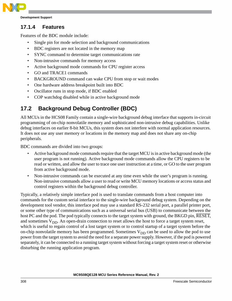
Development Support
17.1.4 Features
Features of the BDC module include:
• Single pin for mode selection and background communications• BDC registers are not located in the memory map• SYNC command to determine target communications rate• Non-intrusive commands for memory access• Active background mode commands for CPU register access• GO and TRACE1 commands• BACKGROUND command can wake CPU from stop or wait modes• One hardware address breakpoint built into BDC• Oscillator runs in stop mode, if BDC enabled• COP watchdog disabled while in active background mode
17.2 Background Debug Controller (BDC)All MCUs in the HCS08 Family contain a single-wire background debug interface that supports in-circuitprogramming of on-chip nonvolatile memory and sophisticated non-intrusive debug capabilities. Unlikedebug interfaces on earlier 8-bit MCUs, this system does not interfere with normal application resources.It does not use any user memory or locations in the memory map and does not share any on-chipperipherals.
BDC commands are divided into two groups:
• Active background mode commands require that the target MCU is in active background mode (theuser program is not running). Active background mode commands allow the CPU registers to beread or written, and allow the user to trace one user instruction at a time, or GO to the user programfrom active background mode.
• Non-intrusive commands can be executed at any time even while the user’s program is running.Non-intrusive commands allow a user to read or write MCU memory locations or access status andcontrol registers within the background debug controller.
Typically, a relatively simple interface pod is used to translate commands from a host computer intocommands for the custom serial interface to the single-wire background debug system. Depending on thedevelopment tool vendor, this interface pod may use a standard RS-232 serial port, a parallel printer port,or some other type of communications such as a universal serial bus (USB) to communicate between thehost PC and the pod. The pod typically connects to the target system with ground, the BKGD pin, RESET,and sometimes VDD. An open-drain connection to reset allows the host to force a target system reset,which is useful to regain control of a lost target system or to control startup of a target system before theon-chip nonvolatile memory has been programmed. Sometimes VDD can be used to allow the pod to usepower from the target system to avoid the need for a separate power supply. However, if the pod is poweredseparately, it can be connected to a running target system without forcing a target system reset or otherwisedisturbing the running application program.
MC9S08QE128 MCU Series Reference Manual, Rev. 2
308 Freescale Semiconductor

Development Support
Figure 17-1. BDM Tool Connector
17.2.1 BKGD Pin Description
BKGD is the single-wire background debug interface pin. The primary function of this pin is forbidirectional serial communication of active background mode commands and data. During reset, this pinis used to select between starting in active background mode or starting the user’s application program.This pin is also used to request a timed sync response pulse to allow a host development tool to determinethe correct clock frequency for background debug serial communications.
BDC serial communications use a custom serial protocol first introduced on the M68HC12 Family ofmicrocontrollers. This protocol assumes the host knows the communication clock rate that is determinedby the target BDC clock rate. All communication is initiated and controlled by the host that drives ahigh-to-low edge to signal the beginning of each bit time. Commands and data are sent most significant bitfirst (MSB first). For a detailed description of the communications protocol, refer to Section 17.2.2,“Communication Details.”
If a host is attempting to communicate with a target MCU that has an unknown BDC clock rate, a SYNCcommand may be sent to the target MCU to request a timed sync response signal from which the host candetermine the correct communication speed.
BKGD is a pseudo-open-drain pin and there is an on-chip pullup so no external pullup resistor is required.Unlike typical open-drain pins, the external RC time constant on this pin, which is influenced by externalcapacitance, plays almost no role in signal rise time. The custom protocol provides for brief, activelydriven speedup pulses to force rapid rise times on this pin without risking harmful drive level conflicts.Refer to Section 17.2.2, “Communication Details,” for more detail.
When no debugger pod is connected to the 6-pin BDM interface connector, the internal pullup on BKGDchooses normal operating mode. When a debug pod is connected to BKGD it is possible to force the MCUinto active background mode after reset. The specific conditions for forcing active background dependupon the HCS08 derivative (refer to the introduction to this Development Support section). It is notnecessary to reset the target MCU to communicate with it through the background debug interface.
17.2.2 Communication Details
The BDC serial interface requires the external controller to generate a falling edge on the BKGD pin toindicate the start of each bit time. The external controller provides this falling edge whether data istransmitted or received.
BKGD is a pseudo-open-drain pin that can be driven either by an external controller or by the MCU. Datais transferred MSB first at 16 BDC clock cycles per bit (nominal speed). The interface times out if512 BDC clock cycles occur between falling edges from the host. Any BDC command that was in progress
2
4
6NO CONNECT 5
NO CONNECT 3
1
RESET
BKGD GND
VDD
MC9S08QE128 MCU Series Reference Manual, Rev. 2
Freescale Semiconductor 309
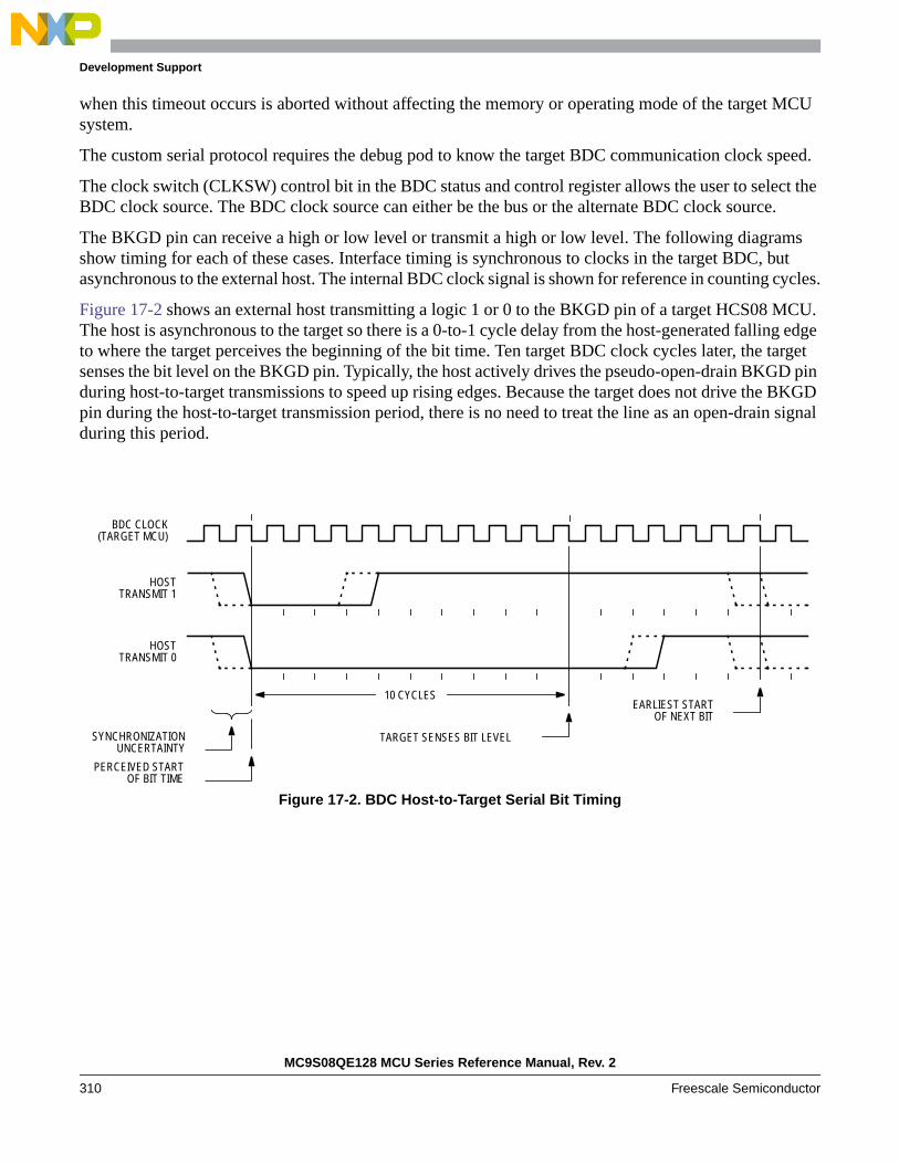
Development Support
when this timeout occurs is aborted without affecting the memory or operating mode of the target MCUsystem.
The custom serial protocol requires the debug pod to know the target BDC communication clock speed.
The clock switch (CLKSW) control bit in the BDC status and control register allows the user to select theBDC clock source. The BDC clock source can either be the bus or the alternate BDC clock source.
The BKGD pin can receive a high or low level or transmit a high or low level. The following diagramsshow timing for each of these cases. Interface timing is synchronous to clocks in the target BDC, butasynchronous to the external host. The internal BDC clock signal is shown for reference in counting cycles.
Figure 17-2 shows an external host transmitting a logic 1 or 0 to the BKGD pin of a target HCS08 MCU.The host is asynchronous to the target so there is a 0-to-1 cycle delay from the host-generated falling edgeto where the target perceives the beginning of the bit time. Ten target BDC clock cycles later, the targetsenses the bit level on the BKGD pin. Typically, the host actively drives the pseudo-open-drain BKGD pinduring host-to-target transmissions to speed up rising edges. Because the target does not drive the BKGDpin during the host-to-target transmission period, there is no need to treat the line as an open-drain signalduring this period.
Figure 17-2. BDC Host-to-Target Serial Bit Timing
EARLIEST START
TARGET SENSES BIT LEVEL
10 CYCLES
SYNCHRONIZATIONUNCERTAINTY
BDC CLOCK(TARGET MCU)
HOSTTRANSMIT 1
HOSTTRANSMIT 0
PERCEIVED STARTOF BIT TIME
OF NEXT BIT
MC9S08QE128 MCU Series Reference Manual, Rev. 2
310 Freescale Semiconductor

Development Support
Figure 17-3 shows the host receiving a logic 1 from the target HCS08 MCU. Because the host isasynchronous to the target MCU, there is a 0-to-1 cycle delay from the host-generated falling edge onBKGD to the perceived start of the bit time in the target MCU. The host holds the BKGD pin low longenough for the target to recognize it (at least two target BDC cycles). The host must release the low drivebefore the target MCU drives a brief active-high speedup pulse seven cycles after the perceived start of thebit time. The host should sample the bit level about 10 cycles after it started the bit time.
Figure 17-3. BDC Target-to-Host Serial Bit Timing (Logic 1)
HOST SAMPLES BKGD PIN
10 CYCLES
BDC CLOCK(TARGET MCU)
HOST DRIVETO BKGD PIN
TARGET MCUSPEEDUP PULSE
PERCEIVED STARTOF BIT TIME
HIGH-IMPEDANCE
HIGH-IMPEDANCE HIGH-IMPEDANCE
BKGD PINR-C RISE
10 CYCLES
EARLIEST STARTOF NEXT BIT
MC9S08QE128 MCU Series Reference Manual, Rev. 2
Freescale Semiconductor 311
Development Support
Figure 17-4 shows the host receiving a logic 0 from the target HCS08 MCU. Because the host isasynchronous to the target MCU, there is a 0-to-1 cycle delay from the host-generated falling edge onBKGD to the start of the bit time as perceived by the target MCU. The host initiates the bit time but thetarget HCS08 finishes it. Because the target wants the host to receive a logic 0, it drives the BKGD pin lowfor 13 BDC clock cycles, then briefly drives it high to speed up the rising edge. The host samples the bitlevel about 10 cycles after starting the bit time.
Figure 17-4. BDM Target-to-Host Serial Bit Timing (Logic 0)
10 CYCLES
BDC CLOCK(TARGET MCU)
HOST DRIVETO BKGD PIN
TARGET MCUDRIVE AND
PERCEIVED STARTOF BIT TIME
HIGH-IMPEDANCE
BKGD PIN
10 CYCLES
SPEED-UP PULSE
SPEEDUPPULSE
EARLIEST STARTOF NEXT BIT
HOST SAMPLES BKGD PIN
MC9S08QE128 MCU Series Reference Manual, Rev. 2
312 Freescale Semiconductor

Development Support
17.2.3 BDC Commands
BDC commands are sent serially from a host computer to the BKGD pin of the target HCS08 MCU. Allcommands and data are sent MSB-first using a custom BDC communications protocol. Active backgroundmode commands require that the target MCU is currently in the active background mode whilenon-intrusive commands may be issued at any time whether the target MCU is in active background modeor running a user application program.
Table 17-1 shows all HCS08 BDC commands, a shorthand description of their coding structure, and themeaning of each command.
Coding Structure Nomenclature
This nomenclature is used in Table 17-1 to describe the coding structure of the BDC commands.
Commands begin with an 8-bit hexadecimal command code in the host-to-targetdirection (most significant bit first)
/ = separates parts of the commandd = delay 16 target BDC clock cycles
AAAA = a 16-bit address in the host-to-target directionRD = 8 bits of read data in the target-to-host direction
WD = 8 bits of write data in the host-to-target directionRD16 = 16 bits of read data in the target-to-host direction
WD16 = 16 bits of write data in the host-to-target directionSS = the contents of BDCSCR in the target-to-host direction (STATUS)CC = 8 bits of write data for BDCSCR in the host-to-target direction (CONTROL)
RBKP = 16 bits of read data in the target-to-host direction (from BDCBKPT breakpointregister)
WBKP = 16 bits of write data in the host-to-target direction (for BDCBKPT breakpoint register)
MC9S08QE128 MCU Series Reference Manual, Rev. 2
Freescale Semiconductor 313
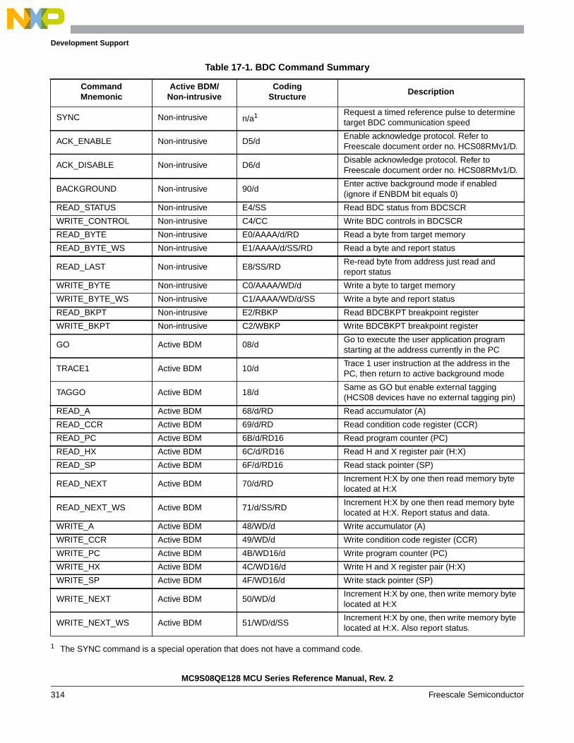
Development Support
Table 17-1. BDC Command Summary
CommandMnemonic
Active BDM/Non-intrusive
CodingStructure
Description
SYNC Non-intrusive n/a1
1 The SYNC command is a special operation that does not have a command code.
Request a timed reference pulse to determinetarget BDC communication speed
ACK_ENABLE Non-intrusive D5/dEnable acknowledge protocol. Refer toFreescale document order no. HCS08RMv1/D.
ACK_DISABLE Non-intrusive D6/dDisable acknowledge protocol. Refer toFreescale document order no. HCS08RMv1/D.
BACKGROUND Non-intrusive 90/dEnter active background mode if enabled(ignore if ENBDM bit equals 0)
READ_STATUS Non-intrusive E4/SS Read BDC status from BDCSCR
WRITE_CONTROL Non-intrusive C4/CC Write BDC controls in BDCSCR
READ_BYTE Non-intrusive E0/AAAA/d/RD Read a byte from target memory
READ_BYTE_WS Non-intrusive E1/AAAA/d/SS/RD Read a byte and report status
READ_LAST Non-intrusive E8/SS/RDRe-read byte from address just read andreport status
WRITE_BYTE Non-intrusive C0/AAAA/WD/d Write a byte to target memory
WRITE_BYTE_WS Non-intrusive C1/AAAA/WD/d/SS Write a byte and report status
READ_BKPT Non-intrusive E2/RBKP Read BDCBKPT breakpoint register
WRITE_BKPT Non-intrusive C2/WBKP Write BDCBKPT breakpoint register
GO Active BDM 08/dGo to execute the user application programstarting at the address currently in the PC
TRACE1 Active BDM 10/dTrace 1 user instruction at the address in thePC, then return to active background mode
TAGGO Active BDM 18/dSame as GO but enable external tagging(HCS08 devices have no external tagging pin)
READ_A Active BDM 68/d/RD Read accumulator (A)
READ_CCR Active BDM 69/d/RD Read condition code register (CCR)
READ_PC Active BDM 6B/d/RD16 Read program counter (PC)
READ_HX Active BDM 6C/d/RD16 Read H and X register pair (H:X)
READ_SP Active BDM 6F/d/RD16 Read stack pointer (SP)
READ_NEXT Active BDM 70/d/RDIncrement H:X by one then read memory bytelocated at H:X
READ_NEXT_WS Active BDM 71/d/SS/RDIncrement H:X by one then read memory bytelocated at H:X. Report status and data.
WRITE_A Active BDM 48/WD/d Write accumulator (A)
WRITE_CCR Active BDM 49/WD/d Write condition code register (CCR)
WRITE_PC Active BDM 4B/WD16/d Write program counter (PC)
WRITE_HX Active BDM 4C/WD16/d Write H and X register pair (H:X)
WRITE_SP Active BDM 4F/WD16/d Write stack pointer (SP)
WRITE_NEXT Active BDM 50/WD/dIncrement H:X by one, then write memory bytelocated at H:X
WRITE_NEXT_WS Active BDM 51/WD/d/SSIncrement H:X by one, then write memory bytelocated at H:X. Also report status.
MC9S08QE128 MCU Series Reference Manual, Rev. 2
314 Freescale Semiconductor
Development Support
The SYNC command is unlike other BDC commands because the host does not necessarily know thecorrect communications speed to use for BDC communications until after it has analyzed the response tothe SYNC command.
To issue a SYNC command, the host:
• Drives the BKGD pin low for at least 128 cycles of the slowest possible BDC clock (The slowestclock is normally the reference oscillator/64 or the self-clocked rate/64.)
• Drives BKGD high for a brief speedup pulse to get a fast rise time (This speedup pulse is typicallyone cycle of the fastest clock in the system.)
• Removes all drive to the BKGD pin so it reverts to high impedance
• Monitors the BKGD pin for the sync response pulse
The target, upon detecting the SYNC request from the host (which is a much longer low time than wouldever occur during normal BDC communications):
• Waits for BKGD to return to a logic high
• Delays 16 cycles to allow the host to stop driving the high speedup pulse
• Drives BKGD low for 128 BDC clock cycles
• Drives a 1-cycle high speedup pulse to force a fast rise time on BKGD
• Removes all drive to the BKGD pin so it reverts to high impedance
The host measures the low time of this 128-cycle sync response pulse and determines the correct speed forsubsequent BDC communications. Typically, the host can determine the correct communication speedwithin a few percent of the actual target speed and the communication protocol can easily tolerate speederrors of several percent.
17.2.4 BDC Hardware Breakpoint
The BDC includes one relatively simple hardware breakpoint that compares the CPU address bus to a16-bit match value in the BDCBKPT register. This breakpoint can generate a forced breakpoint or a taggedbreakpoint. A forced breakpoint causes the CPU to enter active background mode at the first instructionboundary following any access to the breakpoint address. The tagged breakpoint causes the instructionopcode at the breakpoint address to be tagged so that the CPU will enter active background mode ratherthan executing that instruction if and when it reaches the end of the instruction queue. This implies thattagged breakpoints can only be placed at the address of an instruction opcode while forced breakpoints canbe set at any address.
The breakpoint enable (BKPTEN) control bit in the BDC status and control register (BDCSCR) is used toenable the breakpoint logic (BKPTEN = 1). When BKPTEN = 0, its default value after reset, thebreakpoint logic is disabled and no BDC breakpoints are requested regardless of the values in other BDCbreakpoint registers and control bits. The force/tag select (FTS) control bit in BDCSCR is used to selectforced (FTS = 1) or tagged (FTS = 0) type breakpoints.
17.3 Register Definition
This section contains the descriptions of the BDC registers and control bits.
MC9S08QE128 MCU Series Reference Manual, Rev. 2
Freescale Semiconductor 315

Development Support
This section refers to registers and control bits only by their names. A Freescale-provided equate or headerfile is used to translate these names into the appropriate absolute addresses.
17.3.1 BDC Registers and Control Bits
The BDC has two registers:
• The BDC status and control register (BDCSCR) is an 8-bit register containing control and statusbits for the background debug controller.
• The BDC breakpoint match register (BDCBKPT) holds a 16-bit breakpoint match address.
These registers are accessed with dedicated serial BDC commands and are not located in the memoryspace of the target MCU (so they do not have addresses and cannot be accessed by user programs).
Some of the bits in the BDCSCR have write limitations; otherwise, these registers may be read or writtenat any time. For example, the ENBDM control bit may not be written while the MCU is in activebackground mode. (This prevents the ambiguous condition of the control bit forbidding active backgroundmode while the MCU is already in active background mode.) Also, the four status bits (BDMACT, WS,WSF, and DVF) are read-only status indicators and can never be written by the WRITE_CONTROL serialBDC command. The clock switch (CLKSW) control bit may be read or written at any time.
MC9S08QE128 MCU Series Reference Manual, Rev. 2
316 Freescale Semiconductor
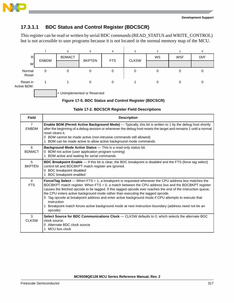
Development Support
Ac
17.3.1.1 BDC Status and Control Register (BDCSCR)
This register can be read or written by serial BDC commands (READ_STATUS and WRITE_CONTROL)but is not accessible to user programs because it is not located in the normal memory map of the MCU.
7 6 5 4 3 2 1 0
RENBDM
BDMACTBKPTEN FTS CLKSW
WS WSF DVF
W
NormalReset
0 0 0 0 0 0 0 0
Reset intive BDM:
1 1 0 0 1 0 0 0
= Unimplemented or Reserved
Figure 17-5. BDC Status and Control Register (BDCSCR)
Table 17-2. BDCSCR Register Field Descriptions
Field Description
7ENBDM
Enable BDM (Permit Active Background Mode) — Typically, this bit is written to 1 by the debug host shortlyafter the beginning of a debug session or whenever the debug host resets the target and remains 1 until a normalreset clears it.0 BDM cannot be made active (non-intrusive commands still allowed)1 BDM can be made active to allow active background mode commands
6BDMACT
Background Mode Active Status — This is a read-only status bit.0 BDM not active (user application program running)1 BDM active and waiting for serial commands
5BKPTEN
BDC Breakpoint Enable — If this bit is clear, the BDC breakpoint is disabled and the FTS (force tag select)control bit and BDCBKPT match register are ignored.0 BDC breakpoint disabled1 BDC breakpoint enabled
4FTS
Force/Tag Select — When FTS = 1, a breakpoint is requested whenever the CPU address bus matches theBDCBKPT match register. When FTS = 0, a match between the CPU address bus and the BDCBKPT registercauses the fetched opcode to be tagged. If this tagged opcode ever reaches the end of the instruction queue,the CPU enters active background mode rather than executing the tagged opcode.0 Tag opcode at breakpoint address and enter active background mode if CPU attempts to execute that
instruction1 Breakpoint match forces active background mode at next instruction boundary (address need not be an
opcode)
3CLKSW
Select Source for BDC Communications Clock — CLKSW defaults to 0, which selects the alternate BDCclock source.0 Alternate BDC clock source1 MCU bus clock
MC9S08QE128 MCU Series Reference Manual, Rev. 2
Freescale Semiconductor 317

Development Support
17.3.1.2 BDC Breakpoint Match Register (BDCBKPT)
This 16-bit register holds the address for the hardware breakpoint in the BDC. The BKPTEN and FTScontrol bits in BDCSCR are used to enable and configure the breakpoint logic. Dedicated serial BDCcommands (READ_BKPT and WRITE_BKPT) are used to read and write the BDCBKPT register but isnot accessible to user programs because it is not located in the normal memory map of the MCU.Breakpoints are normally set while the target MCU is in active background mode before running the userapplication program. For additional information about setup and use of the hardware breakpoint logic inthe BDC, refer to Section 17.2.4, “BDC Hardware Breakpoint.”
17.3.2 System Background Debug Force Reset Register (SBDFR)
This register contains a single write-only control bit. A serial background mode command such asWRITE_BYTE must be used to write to SBDFR. Attempts to write this register from a user program areignored. Reads always return 0x00.
2WS
Wait or Stop Status — When the target CPU is in wait or stop mode, most BDC commands cannot function.However, the BACKGROUND command can be used to force the target CPU out of wait or stop and into activebackground mode where all BDC commands work. Whenever the host forces the target MCU into activebackground mode, the host should issue a READ_STATUS command to check that BDMACT = 1 beforeattempting other BDC commands.0 Target CPU is running user application code or in active background mode (was not in wait or stop mode when
background became active)1 Target CPU is in wait or stop mode, or a BACKGROUND command was used to change from wait or stop to
active background mode
1WSF
Wait or Stop Failure Status — This status bit is set if a memory access command failed due to the target CPUexecuting a wait or stop instruction at or about the same time. The usual recovery strategy is to issue aBACKGROUND command to get out of wait or stop mode into active background mode, repeat the commandthat failed, then return to the user program. (Typically, the host would restore CPU registers and stack values andre-execute the wait or stop instruction.)0 Memory access did not conflict with a wait or stop instruction1 Memory access command failed because the CPU entered wait or stop mode
0DVF
Data Valid Failure Status — This status bit is not used in the MC9S08QE128 Series because it does not haveany slow access memory.0 Memory access did not conflict with a slow memory access1 Memory access command failed because CPU was not finished with a slow memory access
Table 17-2. BDCSCR Register Field Descriptions (continued)
Field Description
MC9S08QE128 MCU Series Reference Manual, Rev. 2
318 Freescale Semiconductor

Development Support
Figure 17-6. System Background Debug Force Reset Register (SBDFR)
7 6 5 4 3 2 1 0
R 0 0 0 0 0 0 0 0
W BDFR1
1 BDFR is writable only through serial background mode debug commands, not from user programs.
Reset 0 0 0 0 0 0 0 0
= Unimplemented or Reserved
Table 17-3. SBDFR Register Field Description
Field Description
0BDFR
Background Debug Force Reset — A serial active background mode command such as WRITE_BYTE allowsan external debug host to force a target system reset. Writing 1 to this bit forces an MCU reset. This bit cannotbe written from a user program.
MC9S08QE128 MCU Series Reference Manual, Rev. 2
Freescale Semiconductor 319

Development Support
MC9S08QE128 MCU Series Reference Manual, Rev. 2
320 Freescale Semiconductor

MC9S08QE128 MCU Series Reference Manual, Rev. 2
Freescale Semiconductor 321
Chapter 18Debug Module (DBG) (128K)
18.1 IntroductionThe DBG module implements an on-chip ICE (in-circuit emulation) system and allows non-intrusivedebug of application software by providing an on-chip trace buffer with flexible triggering capability. Thetrigger also can provide extended breakpoint capacity. The on-chip ICE system is optimized for the HCS088-bit architecture and supports 64K bytes or 128K bytes of memory space.
18.1.1 Features
The on-chip ICE system includes these distinctive features:
• Three comparators (A, B, and C) with ability to match addresses in 128K space
— Dual mode, Comparators A and B used to compare addresses
— Full mode, Comparator A compares address and Comparator B compares data
— Can be used as triggers and/or breakpoints
— Comparator C can be used as a normal hardware breakpoint
— Loop1 capture mode, Comparator C is used to track most recent COF event captured into FIFO
• Tag and Force type breakpoints
• Nine trigger modes
— A
— A Or B
— A Then B
— A And B, where B is data (Full mode)
— A And Not B, where B is data (Full mode)
— Event Only B, store data
— A Then Event Only B, store data
— Inside Range, A ≤ Address ≤ B
— Outside Range, Address < Α or Address > B
• FIFO for storing change of flow information and event only data
— Source address of conditional branches taken
— Destination address of indirect JMP and JSR instruction
— Destination address of interrupts, RTI, RTC, and RTS instruction
— Data associated with Event B trigger modes
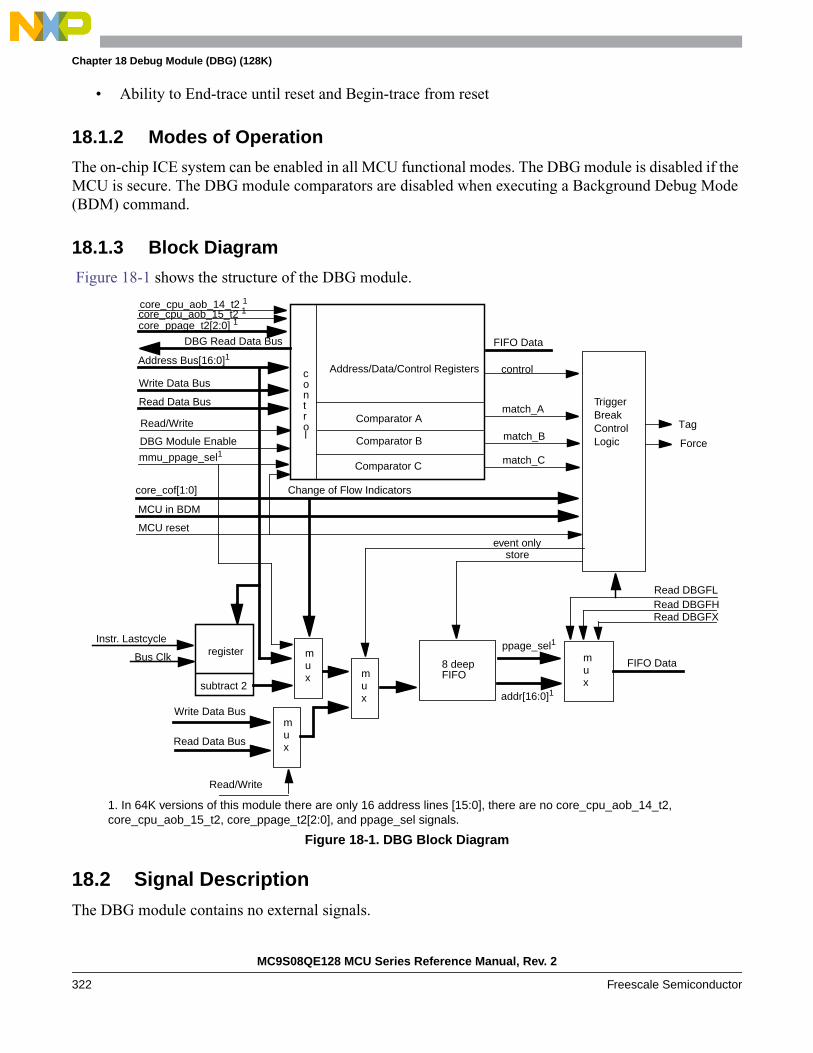
Chapter 18 Debug Module (DBG) (128K)
MC9S08QE128 MCU Series Reference Manual, Rev. 2
322 Freescale Semiconductor
• Ability to End-trace until reset and Begin-trace from reset
18.1.2 Modes of Operation
The on-chip ICE system can be enabled in all MCU functional modes. The DBG module is disabled if theMCU is secure. The DBG module comparators are disabled when executing a Background Debug Mode(BDM) command.
18.1.3 Block Diagram
Figure 18-1 shows the structure of the DBG module.
Figure 18-1. DBG Block Diagram
18.2 Signal DescriptionThe DBG module contains no external signals.
mmu_ppage_sel1
Comparator A
Address/Data/Control Registers
Tag
Force
Address Bus[16:0]1
match_A
control
Read Data Bus
Read/Write
store
mux
FIFO Data
ppage_sel1
MCU in BDM
Change of Flow Indicators
subtract 2
mux
Read DBGFHRead DBGFL
registerInstr. Lastcycle
Bus Clk
Comparator B match_B
8 deepFIFOm
ux
event only
Write Data Bus
TriggerBreakControlLogic
contro
FIFO DataDBG Read Data Bus
DBG Module Enable
addr[16:0]1
mux
Write Data Bus
Read Data Bus
Read/Write
l
Comparator C match_C
MCU reset
core_cof[1:0]
Read DBGFX
1. In 64K versions of this module there are only 16 address lines [15:0], there are no core_cpu_aob_14_t2,core_cpu_aob_15_t2, core_ppage_t2[2:0], and ppage_sel signals.
core_cpu_aob_14_t2 1
core_cpu_aob_15_t2 1
core_ppage_t2[2:0] 1

Chapter 18 Debug Module (DBG) (128K)
MC9S08QE128 MCU Series Reference Manual, Rev. 2
Freescale Semiconductor 323
18.3 Memory Map and RegistersThis section provides a detailed description of all DBG registers accessible to the end user.
18.3.1 Module Memory Map
Table 18-1 shows the registers contained in the DBG module.
Table 18-1. Module Memory Map
Address Use Access
Base + $0000 Debug Comparator A High Register (DBGCAH) Read/write
Base + $0001 Debug Comparator A Low Register (DBGCAL) Read/write
Base + $0002 Debug Comparator B High Register (DBGCBH) Read/write
Base + $0003 Debug Comparator B Low Register (DBGCBL) Read/write
Base + $0004 Debug Comparator C High Register (DBGCCH) Read/write
Base + $0005 Debug Comparator C Low Register (DBGCCL) Read/write
Base + $0006 Debug FIFO High Register (DBGFH) Read only
Base + $0007 Debug FIFO Low Register (DBGFL) Read only
Base + $0008 Debug Comparator A Extension Register (DBGCAX) Read/write
Base + $0009 Debug Comparator B Extension Register (DBGCBX) Read/write
Base + $000A Debug Comparator C Extension Register (DBGCCX) Read/write
Base + $000B Debug FIFO Extended Information Register (DBGFX) Read only
Base + $000C Debug Control Register (DBGC) Read/write
Base + $000D Debug Trigger Register (DBGT) Read/write
Base + $000E Debug Status Register (DBGS) Read only
Base + $000F Debug FIFO Count Register (DBGCNT) Read only

Chapter 18 Debug Module (DBG) (128K)
MC9S08QE128 MCU Series Reference Manual, Rev. 2
324 Freescale Semiconductor
18.3.2Table 18-2. Register Bit Summary
7 6 5 4 3 2 1 0
DBGCAH Bit 15 Bit 14 Bit 13 Bit 12 Bit 11 Bit 10 Bit 9 Bit 8
DBGCAL Bit 7 Bit 6 Bit 5 Bit 4 Bit 3 Bit 2 Bit 1 Bit 0
DBGCBH Bit 15 Bit 14 Bit 13 Bit 12 Bit 11 Bit 10 Bit 9 Bit 8
DBGCBL Bit 7 Bit 6 Bit 5 Bit 4 Bit 3 Bit 2 Bit 1 Bit 0
DBGCCH Bit 15 Bit 14 Bit 13 Bit 12 Bit 11 Bit 10 Bit 9 Bit 8
DBGCCL Bit 7 Bit 6 Bit 5 Bit 4 Bit 3 Bit 2 Bit 1 Bit 0
DBGFH Bit 15 Bit 14 Bit 13 Bit 12 Bit 11 Bit 10 Bit 9 Bit 8
DBGFL Bit 7 Bit 6 Bit 5 Bit 4 Bit 3 Bit 2 Bit 1 Bit 0
DBGCAX RWAEN RWA PAGSEL 0 0 0 0 bit-16
DBGCBX RWBEN RWB PAGSEL 0 0 0 0 bit-16
DBGCCX RWCEN RWC PAGSEL 0 0 0 0 bit-16
DBGFX PPACC 0 0 0 0 0 0 bit-16
DBGC DBGEN ARM TAG BRKEN - - - LOOP1
DBGT TRGSEL BEGIN 0 0 TRG[3:0]
DBGS AF BF CF 0 0 0 0 ARMF
DBGCNT 0 0 0 0 CNT[3:0]
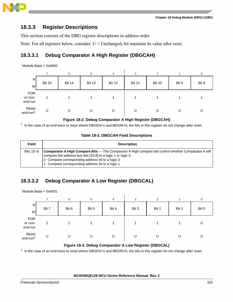
Chapter 18 Debug Module (DBG) (128K)
MC9S08QE128 MCU Series Reference Manual, Rev. 2
Freescale Semiconductor 325
18.3.3 Register Descriptions
This section consists of the DBG register descriptions in address order.
Note: For all registers below, consider: U = Unchanged, bit maintain its value after reset.
18.3.3.1 Debug Comparator A High Register (DBGCAH)
18.3.3.2 Debug Comparator A Low Register (DBGCAL)
Module Base + 0x0000
7 6 5 4 3 2 1 0
RBit 15 Bit 14 Bit 13 Bit 12 Bit 11 Bit 10 Bit 9 Bit 8
W
PORor non-
end-run1 1 1 1 1 1 1 1
Resetend-run1
1 In the case of an end-trace to reset where DBGEN=1 and BEGIN=0, the bits in this register do not change after reset.
U U U U U U U U
Figure 18-2. Debug Comparator A High Register (DBGCAH)
Table 18-3. DBGCAH Field Descriptions
Field Description
Bits 15–8 Comparator A High Compare Bits — The Comparator A High compare bits control whether Comparator A willcompare the address bus bits [15:8] to a logic 1 or logic 0.0 Compare corresponding address bit to a logic 01 Compare corresponding address bit to a logic 1
Module Base + 0x0001
7 6 5 4 3 2 1 0
RBit 7 Bit 6 Bit 5 Bit 4 Bit 3 Bit 2 Bit 1 Bit 0
W
PORor non-
end-run1 1 1 1 1 1 1 0
Resetend-run1
1 In the case of an end-trace to reset where DBGEN=1 and BEGIN=0, the bits in this register do not change after reset.
U U U U U U U U
Figure 18-3. Debug Comparator A Low Register (DBGCAL)

Chapter 18 Debug Module (DBG) (128K)
MC9S08QE128 MCU Series Reference Manual, Rev. 2
326 Freescale Semiconductor
18.3.3.3 Debug Comparator B High Register (DBGCBH)
18.3.3.4 Debug Comparator B Low Register (DBGCBL)
Table 18-4. DBGCAL Field Descriptions
Field Description
Bits 7–0 Comparator A Low Compare Bits — The Comparator A Low compare bits control whether Comparator A willcompare the address bus bits [7:0] to a logic 1 or logic 0.0 Compare corresponding address bit to a logic 01 Compare corresponding address bit to a logic 1
Module Base + 0x0002
7 6 5 4 3 2 1 0
RBit 15 Bit 14 Bit 13 Bit 12 Bit 11 Bit 10 Bit 9 Bit 8
W
PORor non-
end-run0 0 0 0 0 0 0 0
Resetend-run1
1 In the case of an end-trace to reset where DBGEN=1 and BEGIN=0, the bits in this register do not change after reset.
U U U U U U U U
Figure 18-4. Debug Comparator B High Register (DBGCBH)
Table 18-5. DBGCBH Field Descriptions
Field Description
Bits 15–8 Comparator B High Compare Bits — The Comparator B High compare bits control whether Comparator B willcompare the address bus bits [15:8] to a logic 1 or logic 0. Not used in Full mode.0 Compare corresponding address bit to a logic 01 Compare corresponding address bit to a logic 1
Module Base + 0x0003
7 6 5 4 3 2 1 0
RBit 7 Bit 6 Bit 5 Bit 4 Bit 3 Bit 2 Bit 1 Bit 0
W
PORor non-
end-run0 0 0 0 0 0 0 0
Resetend-run1 U U U U U U U U
Figure 18-5. Debug Comparator B Low Register (DBGCBL)
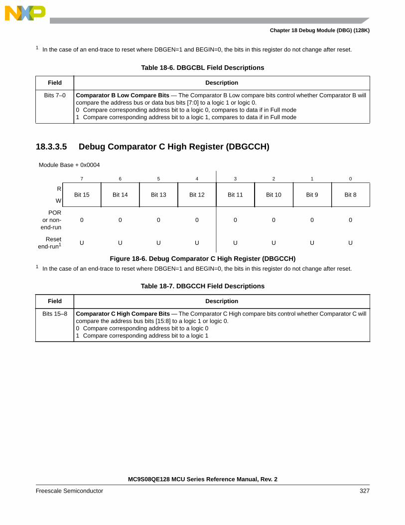
Chapter 18 Debug Module (DBG) (128K)
MC9S08QE128 MCU Series Reference Manual, Rev. 2
Freescale Semiconductor 327
18.3.3.5 Debug Comparator C High Register (DBGCCH)
1 In the case of an end-trace to reset where DBGEN=1 and BEGIN=0, the bits in this register do not change after reset.
Table 18-6. DBGCBL Field Descriptions
Field Description
Bits 7–0 Comparator B Low Compare Bits — The Comparator B Low compare bits control whether Comparator B willcompare the address bus or data bus bits [7:0] to a logic 1 or logic 0.0 Compare corresponding address bit to a logic 0, compares to data if in Full mode1 Compare corresponding address bit to a logic 1, compares to data if in Full mode
Module Base + 0x0004
7 6 5 4 3 2 1 0
RBit 15 Bit 14 Bit 13 Bit 12 Bit 11 Bit 10 Bit 9 Bit 8
W
PORor non-
end-run0 0 0 0 0 0 0 0
Resetend-run1
1 In the case of an end-trace to reset where DBGEN=1 and BEGIN=0, the bits in this register do not change after reset.
U U U U U U U U
Figure 18-6. Debug Comparator C High Register (DBGCCH)
Table 18-7. DBGCCH Field Descriptions
Field Description
Bits 15–8 Comparator C High Compare Bits — The Comparator C High compare bits control whether Comparator C willcompare the address bus bits [15:8] to a logic 1 or logic 0.0 Compare corresponding address bit to a logic 01 Compare corresponding address bit to a logic 1

Chapter 18 Debug Module (DBG) (128K)
MC9S08QE128 MCU Series Reference Manual, Rev. 2
328 Freescale Semiconductor
18.3.3.6 Debug Comparator C Low Register (DBGCCL)
18.3.3.7 Debug FIFO High Register (DBGFH)
Module Base + 0x0005
7 6 5 4 3 2 1 0
RBit 7 Bit 6 Bit 5 Bit 4 Bit 3 Bit 2 Bit 1 Bit 0
W
PORor non-
end-run0 0 0 0 0 0 0 0
Resetend-run1
1 In the case of an end-trace to reset where DBGEN=1 and BEGIN=0, the bits in this register do not change after reset.
U U U U U U U U
Figure 18-7. Debug Comparator C Low Register (DBGCCL)
Table 18-8. DBGCCL Field Descriptions
Field Description
Bits 7–0 Comparator C Low Compare Bits — The Comparator C Low compare bits control whether Comparator C willcompare the address bus bits [7:0] to a logic 1 or logic 0.0 Compare corresponding address bit to a logic 01 Compare corresponding address bit to a logic 1
Module Base + 0x0006
7 6 5 4 3 2 1 0
R Bit 15 Bit 14 Bit 13 Bit 12 Bit 11 Bit 10 Bit 9 Bit 8
W
PORor non-
end-run0 0 0 0 0 0 0 0
Resetend-run1
1 In the case of an end-trace to reset where DBGEN=1 and BEGIN=0, the bits in this register do not change after reset.
U U U U U U U U
= Unimplemented or Reserved
Figure 18-8. Debug FIFO High Register (DBGFH)

Chapter 18 Debug Module (DBG) (128K)
MC9S08QE128 MCU Series Reference Manual, Rev. 2
Freescale Semiconductor 329
18.3.3.8 Debug FIFO Low Register (DBGFL)
Table 18-9. DBGFH Field Descriptions
Field Description
Bits 15–8 FIFO High Data Bits — The FIFO High data bits provide access to bits [15:8] of data in the FIFO. This registeris not used in event only modes and will read a $00 for valid FIFO words.
Module Base + 0x0007
7 6 5 4 3 2 1 0
R Bit 7 Bit 6 Bit 5 Bit 4 Bit 3 Bit 2 Bit 1 Bit 0
W
PORor non-
end-run0 0 0 0 0 0 0 0
Resetend-run1
1 In the case of an end-trace to reset where DBGEN=1 and BEGIN=0, the bits in this register do not change after reset.
U U U U U U U U
= Unimplemented or Reserved
Figure 18-9. Debug FIFO Low Register (DBGFL)
Table 18-10. DBGFL Field Descriptions
Field Description
Bits 7–0 FIFO Low Data Bits — The FIFO Low data bits contain the least significant byte of data in the FIFO. Whenreading FIFO words, read DBGFX and DBGFH before reading DBGFL because reading DBGFL causes theFIFO pointers to advance to the next FIFO location. In event-only modes, there is no useful information in DBGFXand DBGFH so it is not necessary to read them before reading DBGFL.

Chapter 18 Debug Module (DBG) (128K)
MC9S08QE128 MCU Series Reference Manual, Rev. 2
330 Freescale Semiconductor
18.3.3.9 Debug Comparator A Extension Register (DBGCAX)
Module Base + 0x0008
7 6 5 4 3 2 1 0
RRWAEN RWA PAGSEL
0 0 0 0Bit 16
W
PORor non-
end-run0 0 0 0 0 0 0 0
Resetend-run1
1 In the case of an end-trace to reset where DBGEN=1 and BEGIN=0, the bits in this register do not change after reset.
U U U 0 0 0 0 U
= Unimplemented or Reserved
Figure 18-10. Debug Comparator A Extension Register (DBGCAX)
Table 18-11. DBGCAX Field Descriptions
Field Description
7RWAEN
Read/Write Comparator A Enable Bit — The RWAEN bit controls whether read or write comparison is enabledfor Comparator A.0 Read/Write is not used in comparison1 Read/Write is used in comparison
6RWA
Read/Write Comparator A Value Bit — The RWA bit controls whether read or write is used in compare forComparator A. The RWA bit is not used if RWAEN = 0.0 Write cycle will be matched1 Read cycle will be matched
5PAGSEL
Comparator A Page Select Bit — This PAGSEL bit controls whether Comparator A will be qualified with theinternal signal (mmu_ppage_sel) that indicates an extended access through the PPAGE mechanism. Whenmmu_ppage_sel = 1, the 17-bit core address is a paged program access, and the 17-bit core address is madeup of PPAGE[2:0]:addr[13:0]. When mmu_ppage_sel = 0, the 17-bit core address is either a 16-bit CPU addresswith a leading 0 in bit 16, or a 17-bit linear address pointer value.0 Match qualified by mmu_ppage_sel = 0 so address bits [16:0] correspond to a 17-bit CPU address with a
leading zero at bit 16, or a 17-bit linear address pointer address1 Match qualified by mmu_ppage_sel = 1 so address bits [16:0] compare to flash memory address made up of
PPAGE[2:0]:addr[13:0]
0Bit 16
Comparator A Extended Address Bit 16 Compare Bit — The Comparator A bit 16 compare bit controlswhether Comparator A will compare the core address bus bit 16 to a logic 1 or logic 0.0 Compare corresponding address bit to a logic 01 Compare corresponding address bit to a logic 1

Chapter 18 Debug Module (DBG) (128K)
MC9S08QE128 MCU Series Reference Manual, Rev. 2
Freescale Semiconductor 331
18.3.3.10 Debug Comparator B Extension Register (DBGCBX)
Module Base + 0x0009
7 6 5 4 3 2 1 0
RRWBEN RWB PAGSEL
0 0 0 0Bit 16
W
PORor non-
end-run0 0 0 0 0 0 0 0
Resetend-run1
1 In the case of an end-trace to reset where DBGEN=1 and BEGIN=0, the bits in this register do not change after reset.
U U U 0 0 0 0 U
= Unimplemented or Reserved
Figure 18-11. Debug Comparator B Extension Register (DBGCBX)
Table 18-12. DBGCBX Field Descriptions
Field Description
7RWBEN
Read/Write Comparator B Enable Bit — The RWBEN bit controls whether read or write comparison is enabledfor Comparator B. In full modes, RWAEN and RWA are used to control comparison of R/W and RWBEN isignored.0 Read/Write is not used in comparison1 Read/Write is used in comparison
6RWB
Read/Write Comparator B Value Bit — The RWB bit controls whether read or write is used in compare forComparator B. The RWB bit is not used if RWBEN = 0. In full modes, RWAEN and RWA are used to controlcomparison of R/W and RWB is ignored.0 Write cycle will be matched1 Read cycle will be matched
5PAGSEL
Comparator B Page Select Bit — This PAGSEL bit controls whether Comparator B will be qualified with theinternal signal (mmu_papge_sel) that indicates an extended access through the PPAGE mechanism. Whenmmu_ppage_sel = 1, the 17-bit core address is a paged program access, and the 17-bit core address is madeup of PPAGE[2:0]:addr[13:0]. When mmu_papge_sel = 0, the 17-bit core address is either a 16-bit CPU addresswith a leading 0 in bit 16, or a 17-bit linear address pointer value. This bit is not used in full modes wherecomparator B is used to match the data value.0 Match qualified by mmu_ppage_sel = 0 so address bits [16:0] correspond to a 17-bit CPU address with a
leading zero at bit 16, or a 17-bit linear address pointer address1 Match qualified by mmu_ppage_sel = 1 so address bits [16:0] compare to flash memory address made up of
PPAGE[2:0]:addr[13:0]
0Bit 16
Comparator B Extended Address Bit 16 Compare Bit — The Comparator B bit 16 compare bit controlswhether Comparator B will compare the core address bus bit 16 to a logic 1 or logic 0. This bit is not used in fullmodes where comparator B is used to match the data value.0 Compare corresponding address bit to a logic 01 Compare corresponding address bit to a logic 1

Chapter 18 Debug Module (DBG) (128K)
MC9S08QE128 MCU Series Reference Manual, Rev. 2
332 Freescale Semiconductor
18.3.3.11 Debug Comparator C Extension Register (DBGCCX)
Module Base + 0x000A
7 6 5 4 3 2 1 0
RRWCEN RWC PAGSEL
0 0 0 0Bit 16
W
PORor non-
end-run0 0 0 0 0 0 0 0
Resetend-run1
1 In the case of an end-trace to reset where DBGEN=1 and BEGIN=0, the bits in this register do not change after reset.
U U U 0 0 0 0 U
= Unimplemented or Reserved
Figure 18-12. Debug Comparator C Extension Register (DBGCCX)
Table 18-13. DBGCCX Field Descriptions
Field Description
7RWCEN
Read/Write Comparator C Enable Bit — The RWCEN bit controls whether read or write comparison is enabledfor Comparator C.0 Read/Write is not used in comparison1 Read/Write is used in comparison
6RWC
Read/Write Comparator C Value Bit — The RWC bit controls whether read or write is used in compare forComparator C. The RWC bit is not used if RWCEN = 0.0 Write cycle will be matched1 Read cycle will be matched
5PAGSEL
Comparator C Page Select Bit — This PAGSEL bit controls whether Comparator C will be qualified with theinternal signal (mmu_papge_sel) that indicates an extended access through the PPAGE mechanism. Whenmmu_ppage_sel = 1, the 17-bit core address is a paged program access, and the 17-bit core address is madeup of PPAGE[2:0]:addr[13:0]. When mmu_papge_sel = 0, the 17-bit core address is either a 16-bit CPU addresswith a leading 0 in bit 16, or a 17-bit linear address pointer value.0 Match qualified by mmu_ppage_sel = 0 so address bits [16:0] correspond to a 17-bit CPU address with a
leading zero at bit 16, or a 17-bit linear address pointer address1 Match qualified by mmu_ppage_sel = 1 so address bits [16:0] compare to flash memory address made up of
PPAGE[2:0]:addr[13:0]
0Bit 16
Comparator C Extended Address Bit 16 Compare Bit — The Comparator C bit 16 compare bit controlswhether Comparator C will compare the core address bus bit 16 to a logic 1 or logic 0.0 Compare corresponding address bit to a logic 01 Compare corresponding address bit to a logic 1

Chapter 18 Debug Module (DBG) (128K)
MC9S08QE128 MCU Series Reference Manual, Rev. 2
Freescale Semiconductor 333
18.3.3.12 Debug FIFO Extended Information Register (DBGFX)
Module Base + 0x000B
7 6 5 4 3 2 1 0
R PPACC 0 0 0 0 0 0 Bit 16
W
PORor non-
end-run0 0 0 0 0 0 0 0
Resetend-run1
1 In the case of an end-trace to reset where DBGEN=1 and BEGIN=0, the bits in this register do not change after reset.
U 0 0 0 0 0 0 U
= Unimplemented or Reserved
Figure 18-13. Debug FIFO Extended Information Register (DBGFX)
Table 18-14. DBGFX Field Descriptions
Field Description
7PPACC
PPAGE Access Indicator Bit — This bit indicates whether the captured information in the current FIFO word isassociated with an extended access through the PPAGE mechanism or not. This is indicated by the internalsignal mmu_ppage_sel which is 1 when the access is through the PPAGE mechanism.0 The information in the corresponding FIFO word is event-only data or an unpaged 17-bit CPU address with
bit-16 = 01 The information in the corresponding FIFO word is a 17-bit flash address with PPAGE[2:0] in the three most
significant bits and CPU address[13:0] in the 14 least significant bits
0Bit 16
Extended Address Bit 16 — This bit is the most significant bit of the 17-bit core address.

Chapter 18 Debug Module (DBG) (128K)
MC9S08QE128 MCU Series Reference Manual, Rev. 2
334 Freescale Semiconductor
18.3.3.13 Debug Control Register (DBGC)
Module Base + 0x000C
7 6 5 4 3 2 1 0
RDBGEN ARM TAG BRKEN
0 0 0LOOP1
W
PORor non-
end-run1 1 0 0 0 0 0 0
Resetend-run1
1 In the case of an end-trace to reset where DBGEN=1 and BEGIN=0, the ARM and BRKEN bits are cleared but the remainingcontrol bits in this register do not change after reset.
U 0 U 0 0 0 0 U
= Unimplemented or Reserved
Figure 18-14. Debug Control Register (DBGC)
Table 18-15. DBGC Field Descriptions
Field Description
7DBGEN
DBG Module Enable Bit — The DBGEN bit enables the DBG module. The DBGEN bit is forced to zero andcannot be set if the MCU is secure.0 DBG not enabled1 DBG enabled
6ARM
Arm Bit — The ARM bit controls whether the debugger is comparing and storing data in FIFO. SeeSection 18.4.4.2, “Arming the DBG Module” for more information.0 Debugger not armed1 Debugger armed
5TAG
Tag or Force Bit — The TAG bit controls whether a debugger or comparator C breakpoint will be requested asa tag or force breakpoint to the CPU. The TAG bit is not used if BRKEN = 0.0 Force request selected1 Tag request selected
4BRKEN
Break Enable Bit — The BRKEN bit controls whether the debugger will request a breakpoint to the CPU at theend of a trace run, and whether comparator C will request a breakpoint to the CPU.0 CPU break request not enabled1 CPU break request enabled
0LOOP1
Select LOOP1 Capture Mode — This bit selects either normal capture mode or LOOP1 capture mode. LOOP1is not used in event-only modes.0 Normal operation - capture COF events into the capture buffer FIFO1 LOOP1 capture mode enabled. When the conditions are met to store a COF value into the FIFO, compare the
current COF address with the address in comparator C. If these addresses match, override the FIFO captureand do not increment the FIFO count. If the address does not match comparator C, capture the COF address,including the PPACC indicator, into the FIFO and into comparator C.
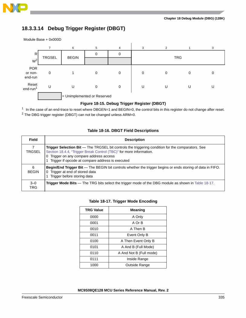
Chapter 18 Debug Module (DBG) (128K)
MC9S08QE128 MCU Series Reference Manual, Rev. 2
Freescale Semiconductor 335
18.3.3.14 Debug Trigger Register (DBGT)
Module Base + 0x000D
7 6 5 4 3 2 1 0
RTRGSEL BEGIN
0 0TRG
W2
PORor non-
end-run0 1 0 0 0 0 0 0
Resetend-run1
1 In the case of an end-trace to reset where DBGEN=1 and BEGIN=0, the control bits in this register do not change after reset.2 The DBG trigger register (DBGT) can not be changed unless ARM=0.
U U 0 0 U U U U
= Unimplemented or Reserved
Figure 18-15. Debug Trigger Register (DBGT)
Table 18-16. DBGT Field Descriptions
Field Description
7TRGSEL
Trigger Selection Bit — The TRGSEL bit controls the triggering condition for the comparators. SeeSection 18.4.4, “Trigger Break Control (TBC)” for more information.0 Trigger on any compare address access1 Trigger if opcode at compare address is executed
6BEGIN
Begin/End Trigger Bit — The BEGIN bit controls whether the trigger begins or ends storing of data in FIFO.0 Trigger at end of stored data1 Trigger before storing data
3–0TRG
Trigger Mode Bits — The TRG bits select the trigger mode of the DBG module as shown in Table 18-17.
Table 18-17. Trigger Mode Encoding
TRG Value Meaning
0000 A Only
0001 A Or B
0010 A Then B
0011 Event Only B
0100 A Then Event Only B
0101 A And B (Full Mode)
0110 A And Not B (Full mode)
0111 Inside Range
1000 Outside Range

Chapter 18 Debug Module (DBG) (128K)
MC9S08QE128 MCU Series Reference Manual, Rev. 2
336 Freescale Semiconductor
NOTEThe DBG trigger register (DBGT) can not be changed unless ARM=0.
18.3.3.15 Debug Status Register (DBGS)
1001↓
1111
No Trigger
Module Base + 0x000E
7 6 5 4 3 2 1 0
R AF BF CF 0 0 0 0 ARMF
W
PORor non-
end-run0 0 0 0 0 0 0 1
Resetend-run1
1 In the case of an end-trace to reset where DBGEN=1 and BEGIN=0, ARMF gets cleared by reset but AF, BF, and CF do notchange after reset.
U U U 0 0 0 0 0
= Unimplemented or Reserved
Figure 18-16. Debug Status Register (DBGS)
Table 18-18. DBGS Field Descriptions
Field Description
7AF
Trigger A Match Bit — The AF bit indicates if Trigger A match condition was met since arming.0 Comparator A did not match1 Comparator A match
6BF
Trigger B Match Bit — The BF bit indicates if Trigger B match condition was met since arming.0 Comparator B did not match1 Comparator B match
5CF
Trigger C Match Bit — The CF bit indicates if Trigger C match condition was met since arming.0 Comparator C did not match1 Comparator C match
0ARMF
Arm Flag Bit — The ARMF bit indicates whether the debugger is waiting for trigger or waiting for the FIFO to fill.While DBGEN = 1, this status bit is a read-only image of the ARM bit in DBGC. See Section 18.4.4.2, “Armingthe DBG Module” for more information.0 Debugger not armed1 Debugger armed
Table 18-17. Trigger Mode Encoding
TRG Value Meaning
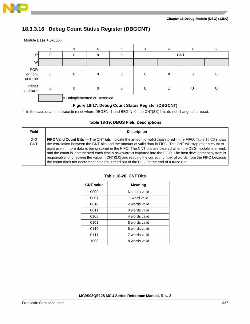
Chapter 18 Debug Module (DBG) (128K)
MC9S08QE128 MCU Series Reference Manual, Rev. 2
Freescale Semiconductor 337
18.3.3.16 Debug Count Status Register (DBGCNT)
Module Base + 0x000F
7 6 5 4 3 2 1 0
R 0 0 0 0 CNT
W
PORor non-
end-run0 0 0 0 0 0 0 0
Resetend-run1
1 In the case of an end-trace to reset where DBGEN=1 and BEGIN=0, the CNT[3:0] bits do not change after reset.
0 0 0 0 U U U U
= Unimplemented or Reserved
Figure 18-17. Debug Count Status Register (DBGCNT)
Table 18-19. DBGS Field Descriptions
Field Description
3–0CNT
FIFO Valid Count Bits — The CNT bits indicate the amount of valid data stored in the FIFO. Table 18-20 showsthe correlation between the CNT bits and the amount of valid data in FIFO. The CNT will stop after a count toeight even if more data is being stored in the FIFO. The CNT bits are cleared when the DBG module is armed,and the count is incremented each time a new word is captured into the FIFO. The host development system isresponsible for checking the value in CNT[3:0] and reading the correct number of words from the FIFO becausethe count does not decrement as data is read out of the FIFO at the end of a trace run.
Table 18-20. CNT Bits
CNT Value Meaning
0000 No data valid
0001 1 word valid
0010 2 words valid
0011 3 words valid
0100 4 words valid
0101 5 words valid
0110 6 words valid
0111 7 words valid
1000 8 words valid
Chapter 18 Debug Module (DBG) (128K)
MC9S08QE128 MCU Series Reference Manual, Rev. 2
338 Freescale Semiconductor
18.4 Functional DescriptionThis section provides a complete functional description of the on-chip ICE system. The DBG module isenabled by setting the DBGEN bit in the DBGC register. Enabling the module allows the arming,triggering and storing of data in the FIFO. The DBG module is made up of three main blocks, theComparators, Trigger Break Control logic and the FIFO.
18.4.1 Comparator
The DBG module contains three comparators, A, B, and C. Comparator A compares the core address buswith the address stored in the DBGCAX, DBGCAH, and DBGCAL registers. Comparator B compares thecore address bus with the address stored in the DBGCBX, DBGCBH, and DBGCBL registers except infull mode, where it compares the data buses to the data stored in the DBGCBL register. Comparator Ccompares the core address bus with the address stored in the DBGCCX, DBGCCH, and DBGCCLregisters. Matches on Comparators A, B, and C are signaled to the Trigger Break Control (TBC) block.
18.4.1.1 RWA and RWAEN in Full Modes
In full modes ("A And B" and "A And Not B") RWAEN and RWA are used to select read or writecomparisons for both comparators A and B. To select write comparisons and the write data bus in FullModes set RWAEN=1 and RWA=0, otherwise read comparisons and the read data bus will be selected.The RWBEN and RWB bits are not used and will be ignored in Full Modes.
18.4.1.2 Comparator C in LOOP1 Capture Mode
Normally comparator C is used as a third hardware breakpoint and is not involved in the trigger logic forthe on-chip ICE system. In this mode, it compares the core address bus with the address stored in theDBGCCX, DBGCCH, and DBGCCL registers. However, in LOOP1 capture mode, comparator C ismanaged by logic in the DBG module to track the address of the most recent change-of-flow event thatwas captured into the FIFO buffer. In LOOP1 capture mode, comparator C is not available for use as anormal hardware breakpoint.
When the ARM and DBGEN bits are set to one in LOOP1 capture mode, comparator C value registers arecleared to prevent the previous contents of these registers from interfering with the LOOP1 capture modeoperation. When a COF event is detected, the address of the event is compared to the contents of theDBGCCX, DBGCCH, and DBGCCL registers to determine whether it is the same as the previous COFentry in the capture FIFO. If the values match, the capture is inhibited to prevent the FIFO from filling upwith duplicate entries. If the values do not match, the COF event is captured into the FIFO and theDBGCCX, DBGCCH, and DBGCCL registers are updated to reflect the address of the captured COFevent. When comparator C is updated, the PAGSEL bit (bit-7 of DBGCCX) is updated with the PPACCvalue that is captured into the FIFO. This bit indicates whether the COF address was a paged 17-bitprogram address using the PPAGE mechanism (PPACC=1) or a 17-bit CPU address that resulted from anunpaged CPU access.
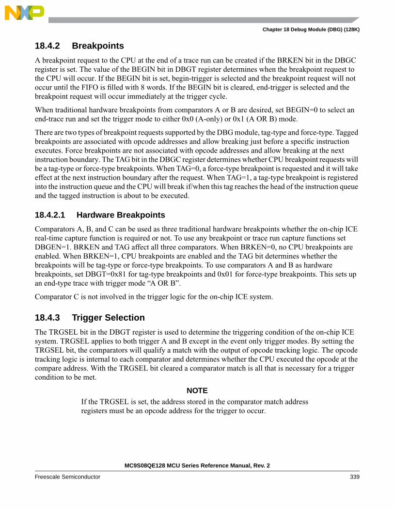
Chapter 18 Debug Module (DBG) (128K)
MC9S08QE128 MCU Series Reference Manual, Rev. 2
Freescale Semiconductor 339
18.4.2 Breakpoints
A breakpoint request to the CPU at the end of a trace run can be created if the BRKEN bit in the DBGCregister is set. The value of the BEGIN bit in DBGT register determines when the breakpoint request tothe CPU will occur. If the BEGIN bit is set, begin-trigger is selected and the breakpoint request will notoccur until the FIFO is filled with 8 words. If the BEGIN bit is cleared, end-trigger is selected and thebreakpoint request will occur immediately at the trigger cycle.
When traditional hardware breakpoints from comparators A or B are desired, set BEGIN=0 to select anend-trace run and set the trigger mode to either 0x0 (A-only) or 0x1 (A OR B) mode.
There are two types of breakpoint requests supported by the DBG module, tag-type and force-type. Taggedbreakpoints are associated with opcode addresses and allow breaking just before a specific instructionexecutes. Force breakpoints are not associated with opcode addresses and allow breaking at the nextinstruction boundary. The TAG bit in the DBGC register determines whether CPU breakpoint requests willbe a tag-type or force-type breakpoints. When TAG=0, a force-type breakpoint is requested and it will takeeffect at the next instruction boundary after the request. When TAG=1, a tag-type breakpoint is registeredinto the instruction queue and the CPU will break if/when this tag reaches the head of the instruction queueand the tagged instruction is about to be executed.
18.4.2.1 Hardware Breakpoints
Comparators A, B, and C can be used as three traditional hardware breakpoints whether the on-chip ICEreal-time capture function is required or not. To use any breakpoint or trace run capture functions setDBGEN=1. BRKEN and TAG affect all three comparators. When BRKEN=0, no CPU breakpoints areenabled. When BRKEN=1, CPU breakpoints are enabled and the TAG bit determines whether thebreakpoints will be tag-type or force-type breakpoints. To use comparators A and B as hardwarebreakpoints, set DBGT=0x81 for tag-type breakpoints and 0x01 for force-type breakpoints. This sets upan end-type trace with trigger mode “A OR B”.
Comparator C is not involved in the trigger logic for the on-chip ICE system.
18.4.3 Trigger Selection
The TRGSEL bit in the DBGT register is used to determine the triggering condition of the on-chip ICEsystem. TRGSEL applies to both trigger A and B except in the event only trigger modes. By setting theTRGSEL bit, the comparators will qualify a match with the output of opcode tracking logic. The opcodetracking logic is internal to each comparator and determines whether the CPU executed the opcode at thecompare address. With the TRGSEL bit cleared a comparator match is all that is necessary for a triggercondition to be met.
NOTEIf the TRGSEL is set, the address stored in the comparator match addressregisters must be an opcode address for the trigger to occur.

Chapter 18 Debug Module (DBG) (128K)
MC9S08QE128 MCU Series Reference Manual, Rev. 2
340 Freescale Semiconductor
18.4.4 Trigger Break Control (TBC)
The TBC is the main controller for the DBG module. Its function is to decide whether data should be storedin the FIFO based on the trigger mode and the match signals from the comparator. The TBC alsodetermines whether a request to break the CPU should occur.
The TAG bit in DBGC controls whether CPU breakpoints are treated as tag-type or force-type breakpoints.The TRGSEL bit in DBGT controls whether a comparator A or B match is further qualified by opcodetracking logic. Each comparator has a separate circuit to track opcodes because the comparators couldcorrespond to separate instructions that could be propagating through the instruction queue at the sametime.
In end-type trace runs (BEGIN=0), when the comparator registers match, including the optional R/Wmatch, this signal goes to the CPU break logic where BRKEN determines whether a CPU break isrequested and the TAG control bit determines whether the CPU break will be a tag-type or force-typebreakpoint. When TRGSEL is set, the R/W qualified comparator match signal also passes through theopcode tracking logic. If/when it propagates through this logic, it will cause a trigger to the ICE logic tobegin or end capturing information into the FIFO. In the case of an end-type (BEGIN=0) trace run, thequalified comparator signal stops the FIFO from capturing any more information.
If a CPU breakpoint is also enabled, you would want TAG and TRGSEL to agree so that the CPU breakoccurs at the same place in the application program as the FIFO stopped capturing information. IfTRGSEL was 0 and TAG was 1 in an end-type trace run, the FIFO would stop capturing as soon as thecomparator address matched, but the CPU would continue running until a TAG signal could propagatethrough the CPUs instruction queue which could take a long time in the case where changes of flow causedthe instruction queue to be flushed. If TRGSEL was one and TAG was zero in an end-type trace run, theCPU would break before the comparator match signal could propagate through the opcode tracking logicto end the trace run.
In begin-type trace runs (BEGIN=1), the start of FIFO capturing is triggered by the qualified comparatorsignals, and the CPU breakpoint (if enabled by BRKEN=1) is triggered when the FIFO becomes full. Sincethis FIFO full condition does not correspond to the execution of a tagged instruction, it would not makesense to use TAG=1 for a begin-type trace run.
18.4.4.1 Begin- and End-Trigger
The definition of begin- and end-trigger as used in the DBG module are as follows:
• Begin-trigger: Storage in FIFO occurs after the trigger and continues until 8 locations are filled.
• End-trigger: Storage in FIFO occurs until the trigger with the least recent data falling out of theFIFO if more than 8 words are collected.
18.4.4.2 Arming the DBG Module
Arming occurs by enabling the DBG module by setting the DBGEN bit and by setting the ARM bit in theDBGC register. The ARM bit in the DBGC register and the ARMF bit in the DBGS register are clearedwhen the trigger condition is met in end-trigger mode or when the FIFO is filled in begin-trigger mode. Inthe case of an end-trace where DBGEN=1 and BEGIN=0, ARM and ARMF are cleared by any reset to
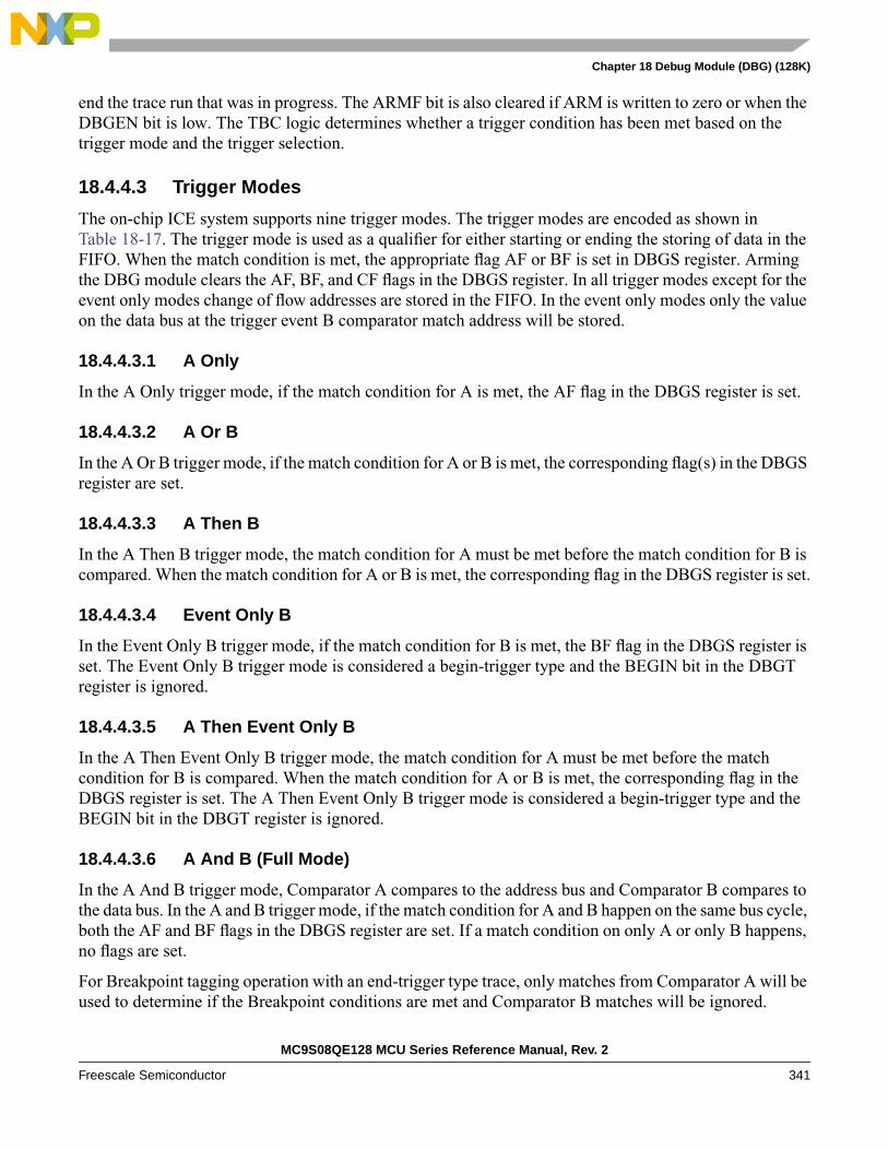
Chapter 18 Debug Module (DBG) (128K)
MC9S08QE128 MCU Series Reference Manual, Rev. 2
Freescale Semiconductor 341
end the trace run that was in progress. The ARMF bit is also cleared if ARM is written to zero or when theDBGEN bit is low. The TBC logic determines whether a trigger condition has been met based on thetrigger mode and the trigger selection.
18.4.4.3 Trigger Modes
The on-chip ICE system supports nine trigger modes. The trigger modes are encoded as shown inTable 18-17. The trigger mode is used as a qualifier for either starting or ending the storing of data in theFIFO. When the match condition is met, the appropriate flag AF or BF is set in DBGS register. Armingthe DBG module clears the AF, BF, and CF flags in the DBGS register. In all trigger modes except for theevent only modes change of flow addresses are stored in the FIFO. In the event only modes only the valueon the data bus at the trigger event B comparator match address will be stored.
18.4.4.3.1 A Only
In the A Only trigger mode, if the match condition for A is met, the AF flag in the DBGS register is set.
18.4.4.3.2 A Or B
In the A Or B trigger mode, if the match condition for A or B is met, the corresponding flag(s) in the DBGSregister are set.
18.4.4.3.3 A Then B
In the A Then B trigger mode, the match condition for A must be met before the match condition for B iscompared. When the match condition for A or B is met, the corresponding flag in the DBGS register is set.
18.4.4.3.4 Event Only B
In the Event Only B trigger mode, if the match condition for B is met, the BF flag in the DBGS register isset. The Event Only B trigger mode is considered a begin-trigger type and the BEGIN bit in the DBGTregister is ignored.
18.4.4.3.5 A Then Event Only B
In the A Then Event Only B trigger mode, the match condition for A must be met before the matchcondition for B is compared. When the match condition for A or B is met, the corresponding flag in theDBGS register is set. The A Then Event Only B trigger mode is considered a begin-trigger type and theBEGIN bit in the DBGT register is ignored.
18.4.4.3.6 A And B (Full Mode)
In the A And B trigger mode, Comparator A compares to the address bus and Comparator B compares tothe data bus. In the A and B trigger mode, if the match condition for A and B happen on the same bus cycle,both the AF and BF flags in the DBGS register are set. If a match condition on only A or only B happens,no flags are set.
For Breakpoint tagging operation with an end-trigger type trace, only matches from Comparator A will beused to determine if the Breakpoint conditions are met and Comparator B matches will be ignored.
Chapter 18 Debug Module (DBG) (128K)
MC9S08QE128 MCU Series Reference Manual, Rev. 2
342 Freescale Semiconductor
18.4.4.3.7 A And Not B (Full Mode)
In the A And Not B trigger mode, comparator A compares to the address bus and comparator B comparesto the data bus. In the A And Not B trigger mode, if the match condition for A and Not B happen on thesame bus cycle, both the AF and BF flags in the DBGS register are set. If a match condition on only A oronly Not B occur no flags are set.
For Breakpoint tagging operation with an end-trigger type trace, only matches from Comparator A will beused to determine if the Breakpoint conditions are met and Comparator B matches will be ignored.
18.4.4.3.8 Inside Range, A ≤ address ≤ B
In the Inside Range trigger mode, if the match condition for A and B happen on the same bus cycle, boththe AF and BF flags in the DBGS register are set. If a match condition on only A or only B occur no flagsare set.
18.4.4.3.9 Outside Range, address < A or address > B
In the Outside Range trigger mode, if the match condition for A or B is met, the corresponding flag in theDBGS register is set.
The four control bits BEGIN and TRGSEL in DBGT, and BRKEN and TAG in DBGC, determine the basictype of debug run as shown in Table 1.21. Some of the 16 possible combinations are not used (refer to thenotes at the end of the table).
Table 18-21. Basic Types of Debug Runs
BEGIN TRGSEL BRKEN TAG Type of Debug Run
0 0 0 x(1) Fill FIFO until trigger address (No CPU breakpoint - keep
running)
0 0 1 0 Fill FIFO until trigger address, then force CPU breakpoint
0 0 1 1 Do not use(2)
0 1 0 x(1) Fill FIFO until trigger opcode about to execute (No CPU
breakpoint - keep running)
0 1 1 0 Do not use(3)
0 1 1 1 Fill FIFO until trigger opcode about to execute (trigger causesCPU breakpoint)
1 0 0 x(1) Start FIFO at trigger address (No CPU breakpoint - keep
running)
1 0 1 0 Start FIFO at trigger address, force CPU breakpoint whenFIFO full
1 0 1 1 Do not use(4)
1 1 0 x(1) Start FIFO at trigger opcode (No CPU breakpoint - keep
running)
1 1 1 0 Start FIFO at trigger opcode, force CPU breakpoint when FIFOfull
1 1 1 1 Do not use(4)
Chapter 18 Debug Module (DBG) (128K)
MC9S08QE128 MCU Series Reference Manual, Rev. 2
Freescale Semiconductor 343
1 When BRKEN = 0, TAG is do not care (x in the table).2 In end trace configurations (BEGIN = 0) where a CPU breakpoint is enabled (BRKEN = 1), TRGSEL should agree with TAG. In this case, whereTRGSEL = 0 to select no opcode tracking qualification and TAG = 1 to specify a tag-type CPU breakpoint, the CPU breakpoint would not takeeffect until sometime after the FIFO stopped storing values. Depending on program loops or interrupts, the delay could be very long.3 In end trace configurations (BEGIN = 0) where a CPU breakpoint is enabled (BRKEN = 1), TRGSEL should agree with TAG. In this case, whereTRGSEL = 1 to select opcode tracking qualification and TAG = 0 to specify a force-type CPU breakpoint, the CPU breakpoint would erroneouslytake effect before the FIFO stopped storing values and the debug run would not complete normally.
4 In begin trace configurations (BEGIN = 1) where a CPU breakpoint is enabled (BRKEN = 1), TAG should not be set to 1. In begin trace debugruns, the CPU breakpoint corresponds to the FIFO full condition which does not correspond to a taggable instruction fetch.
18.4.5 FIFO
The FIFO is an eight word deep FIFO. In all trigger modes except for event only, the data stored in theFIFO will be change of flow addresses. In the event only trigger modes only the data bus valuecorresponding to the event is stored. In event only trigger modes, the high byte of the valid data from theFIFO will always read a 0x00 and the extended information byte in DBGFX will always read 0x00.
18.4.5.1 Storing Data in FIFO
In all trigger modes except for the event only modes, the address stored in the FIFO will be determined bythe change of flow indicators from the core. The signal core_cof[1] indicates the current core address isthe destination address of an indirect JSR or JMP instruction, or a RTS, RTC, or RTI instruction or interruptvector and the destination address should be stored. The signal core_cof[0] indicates that a conditionalbranch was taken and that the source address of the conditional branch should be stored.
18.4.5.2 Storing with Begin-Trigger
Storing with Begin-Trigger can be used in all trigger modes. Once the DBG module is enabled and armedin the begin-trigger mode, data is not stored in the FIFO until the trigger condition is met. Once the triggercondition is met the DBG module will remain armed until 8 words are stored in the FIFO. If thecore_cof[1] signal becomes asserted, the current address is stored in the FIFO. If the core_cof[0] signalbecomes asserted, the address registered during the previous last cycle is decremented by two and storedin the FIFO.
18.4.5.3 Storing with End-Trigger
Storing with End-Trigger cannot be used in event-only trigger modes. Once the DBG module is enabledand armed in the end-trigger mode, data is stored in the FIFO until the trigger condition is met. If thecore_cof[1] signal becomes asserted, the current address is stored in the FIFO. If the core_cof[0] signalbecomes asserted, the address registered during the previous last cycle is decremented by two and storedin the FIFO. When the trigger condition is met, the ARM and ARMF will be cleared and no more data willbe stored. In non-event only end-trigger modes, if the trigger is at a change of flow address the trigger eventwill be stored in the FIFO.
18.4.5.4 Reading Data from FIFO
The data stored in the FIFO can be read using BDM commands provided the DBG module is enabled andnot armed (DBGEN=1 and ARM=0). The FIFO data is read out first-in-first-out. By reading the CNT bits

Chapter 18 Debug Module (DBG) (128K)
MC9S08QE128 MCU Series Reference Manual, Rev. 2
344 Freescale Semiconductor
in the DBGCNT register at the end of a trace run, the number of valid words can be determined. The FIFOdata is read by optionally reading the DBGFX and DBGFH registers followed by the DBGFL register.Each time the DBGFL register is read the FIFO is shifted to allow reading of the next word however thecount does not decrement. In event-only trigger modes where the FIFO will contain only the data busvalues stored, to read the FIFO only DBGFL needs to be accessed.
The FIFO is normally only read while ARM and ARMF=0, however reading the FIFO while the DBGmodule is armed will return the data value in the oldest location of the FIFO and the TBC will not allowthe FIFO to shift. This action could cause a valid entry to be lost because the unexpected read blocked theFIFO advance.
If the DBG module is not armed and the DBGFL register is read, the TBC will store the current opcodeaddress. Through periodic reads of the DBGFX, DBGFH, and DBGFL registers while the DBG moduleis not armed, host software can provide a histogram of program execution. This is called profile mode.Since the full 17-bit address and the signal that indicates whether an address is in paged extended memoryare captured on each FIFO store, profile mode works correctly over the entire extended memory map.
18.4.6 Interrupt Priority
When TRGSEL is set and the DBG module is armed to trigger on begin- or end-trigger types, a trigger isnot detected in the condition where a pending interrupt occurs at the same time that a target address reachesthe top of the instruction pipe. In these conditions, the pending interrupt has higher priority and codeexecution switches to the interrupt service routine.
When TRGSEL is clear and the DBG module is armed to trigger on end-trigger types, the trigger event isdetected on a program fetch of the target address, even when an interrupt becomes pending on the samecycle. In these conditions, the pending interrupt has higher priority, the exception is processed by the coreand the interrupt vector is fetched. Code execution is halted before the first instruction of the interruptservice routine is executed. In this scenario, the DBG module will have cleared ARM without havingrecorded the change-of-flow that occurred as part of the interrupt exception. Note that the stack will holdthe return addresses and can be used to reconstruct execution flow in this scenario.
When TRGSEL is clear and the DBG module is armed to trigger on begin-trigger types, the trigger eventis detected on a program fetch of the target address, even when an interrupt becomes pending on the samecycle. In this scenario, the FIFO captures the change of flow event. Because the system is configured forbegin-trigger, the DBG remains armed and does not break until the FIFO has been filled by subsequentchange of flow events.
18.5 ResetsThe DBG module cannot cause an MCU reset.
There are two different ways this module will respond to reset depending upon the conditions before thereset event. If the DBG module was setup for an end trace run with DBGEN=1 and BEGIN=0, ARM,ARMF, and BRKEN are cleared but the reset function on most DBG control and status bits is overriddenso a host development system can read out the results of the trace run after the MCU has been reset. In allother cases including POR, the DBG module controls are initialized to start a begin trace run starting fromwhen the reset vector is fetched. The conditions for the default begin trace run are:

Chapter 18 Debug Module (DBG) (128K)
MC9S08QE128 MCU Series Reference Manual, Rev. 2
Freescale Semiconductor 345
• DBGCAX=0x00, DBGCAH=0xFF, DBGCAL=0xFE so comparator A is set to match when the16-bit CPU address 0xFFFE appears during the reset vector fetch
• DBGC=0xC0 to enable and arm the DBG module
• DBGT=0x40 to select a force-type trigger, a BEGIN trigger, and A-only trigger mode
18.6 InterruptsThe DBG contains no interrupt source.
18.7 Electrical SpecificationsThe DBG module contain no electrical specifications.

MC9S08QE128RMRev. 2, 05/2007
How to Reach Us:
Home Page:www.freescale.com
E-mail:[email protected]
USA/Europe or Locations Not Listed:Freescale SemiconductorTechnical Information Center, CH3701300 N. Alma School RoadChandler, Arizona 85224+1-800-521-6274 or [email protected]
Europe, Middle East, and Africa:Freescale Halbleiter Deutschland GmbHTechnical Information CenterSchatzbogen 781829 Muenchen, Germany+44 1296 380 456 (English)+46 8 52200080 (English)+49 89 92103 559 (German)+33 1 69 35 48 48 (French)[email protected]
Japan:Freescale Semiconductor Japan Ltd.HeadquartersARCO Tower 15F1-8-1, Shimo-Meguro, Meguro-ku,Tokyo 153-0064Japan0120 191014 or +81 3 5437 [email protected]
Asia/Pacific:Freescale Semiconductor Hong Kong Ltd.Technical Information Center2 Dai King StreetTai Po Industrial EstateTai Po, N.T., Hong Kong+800 2666 [email protected]
For Literature Requests Only:Freescale Semiconductor Literature Distribution CenterP.O. Box 5405Denver, Colorado 802171-800-441-2447 or 303-675-2140Fax: [email protected]
Information in this document is provided solely to enable system and softwareimplementers to use Freescale Semiconductor products. There are no express orimplied copyright licenses granted hereunder to design or fabricate any integratedcircuits or integrated circuits based on the information in this document.
Freescale Semiconductor reserves the right to make changes without further notice toany products herein. Freescale Semiconductor makes no warranty, representation orguarantee regarding the suitability of its products for any particular purpose, nor doesFreescale Semiconductor assume any liability arising out of the application or use of anyproduct or circuit, and specifically disclaims any and all liability, including withoutlimitation consequential or incidental damages. “Typical” parameters that may beprovided in Freescale Semiconductor data sheets and/or specifications can and do varyin different applications and actual performance may vary over time. All operatingparameters, including “Typicals”, must be validated for each customer application bycustomer’s technical experts. Freescale Semiconductor does not convey any licenseunder its patent rights nor the rights of others. Freescale Semiconductor products arenot designed, intended, or authorized for use as components in systems intended forsurgical implant into the body, or other applications intended to support or sustain life,or for any other application in which the failure of the Freescale Semiconductor productcould create a situation where personal injury or death may occur. Should Buyerpurchase or use Freescale Semiconductor products for any such unintended orunauthorized application, Buyer shall indemnify and hold Freescale Semiconductor andits officers, employees, subsidiaries, affiliates, and distributors harmless against allclaims, costs, damages, and expenses, and reasonable attorney fees arising out of,directly or indirectly, any claim of personal injury or death associated with suchunintended or unauthorized use, even if such claim alleges that FreescaleSemiconductor was negligent regarding the design or manufacture of the part.
Freescale™ and the Freescale logo are trademarks of Freescale Semiconductor, Inc.All other product or service names are the property of their respective owners.
© Freescale Semiconductor, Inc. 2007. All rights reserved.