
MC56F8367EVMUM
80
56F8300 16-bit Digital Signal Controllers freescale.com 56F8367 Evaluation Module User Manual MC56F8367EVMUM Rev. 2 07/2005
-
Upload
iverson278 -
Category
Documents
-
view
6 -
download
0
Transcript of MC56F8367EVMUM

56F830016-bit Digital Signal Controllers
freescale.com
56F8367Evaluation Module User Manual
MC56F8367EVMUMRev. 207/2005

Document Revision History
Version History Description of Change
Rev 1.0 Initial Public Release
Rev 2.0 Updated look and feel

TABLE OF CONTENTS
Table of Contents, Rev. 2
Freescale Semiconductor i Preliminary
Preface Preface-vii
Chapter 1 Introduction
1.1 56F8367EVM Architecture. . . . . . . . . . . . . . . . . . . . . . . . . . . . . . . . . . . . . . . . . . . . . . . 1-21.2 56F8367EVM Configuration Jumpers . . . . . . . . . . . . . . . . . . . . . . . . . . . . . . . . . . . . . . 1-31.3 56F8367EVM Connections. . . . . . . . . . . . . . . . . . . . . . . . . . . . . . . . . . . . . . . . . . . . . . . 1-5
Chapter 2 Technical Summary
2.1 MC56F8367 . . . . . . . . . . . . . . . . . . . . . . . . . . . . . . . . . . . . . . . . . . . . . . . . . . . . . . . . . . 2-42.2 Program and Data Memory. . . . . . . . . . . . . . . . . . . . . . . . . . . . . . . . . . . . . . . . . . . . . . . 2-42.2.1 SRAM Bank 0 . . . . . . . . . . . . . . . . . . . . . . . . . . . . . . . . . . . . . . . . . . . . . . . . . . . . . . 2-52.2.2 SRAM Bank 1 . . . . . . . . . . . . . . . . . . . . . . . . . . . . . . . . . . . . . . . . . . . . . . . . . . . . . . 2-62.3 RS-232 Serial Communications . . . . . . . . . . . . . . . . . . . . . . . . . . . . . . . . . . . . . . . . . . . 2-72.4 Clock Source . . . . . . . . . . . . . . . . . . . . . . . . . . . . . . . . . . . . . . . . . . . . . . . . . . . . . . . . . . 2-82.5 Operating Mode . . . . . . . . . . . . . . . . . . . . . . . . . . . . . . . . . . . . . . . . . . . . . . . . . . . . . . . 2-92.5.1 EXTBOOT. . . . . . . . . . . . . . . . . . . . . . . . . . . . . . . . . . . . . . . . . . . . . . . . . . . . . . . . . 2-92.5.2 EMI_MODE . . . . . . . . . . . . . . . . . . . . . . . . . . . . . . . . . . . . . . . . . . . . . . . . . . . . . . . 2-92.5.3 CLKMODE . . . . . . . . . . . . . . . . . . . . . . . . . . . . . . . . . . . . . . . . . . . . . . . . . . . . . . . 2-102.6 Debug LEDs . . . . . . . . . . . . . . . . . . . . . . . . . . . . . . . . . . . . . . . . . . . . . . . . . . . . . . . . . 2-102.7 Debug Support . . . . . . . . . . . . . . . . . . . . . . . . . . . . . . . . . . . . . . . . . . . . . . . . . . . . . . . 2-112.7.1 JTAG Connector . . . . . . . . . . . . . . . . . . . . . . . . . . . . . . . . . . . . . . . . . . . . . . . . . . . 2-122.7.2 Parallel JTAG Interface Connector . . . . . . . . . . . . . . . . . . . . . . . . . . . . . . . . . . . . . 2-132.8 External Interrupts. . . . . . . . . . . . . . . . . . . . . . . . . . . . . . . . . . . . . . . . . . . . . . . . . . . . . 2-152.9 Reset . . . . . . . . . . . . . . . . . . . . . . . . . . . . . . . . . . . . . . . . . . . . . . . . . . . . . . . . . . . . . . . 2-162.10 Power Supply . . . . . . . . . . . . . . . . . . . . . . . . . . . . . . . . . . . . . . . . . . . . . . . . . . . . . . . . 2-172.11 Daughter Card Connectors . . . . . . . . . . . . . . . . . . . . . . . . . . . . . . . . . . . . . . . . . . . . . . 2-182.11.1 Peripheral Daughter Card Connector . . . . . . . . . . . . . . . . . . . . . . . . . . . . . . . . . . . 2-182.11.2 Memory Daughter Card Connector . . . . . . . . . . . . . . . . . . . . . . . . . . . . . . . . . . . . . 2-202.12 Motor Control PWM Signals and LEDs . . . . . . . . . . . . . . . . . . . . . . . . . . . . . . . . . . . . 2-22

MC56F8367EVM User Manual, Rev. 2
ii Freescale Semiconductor Preliminary
2.13 CAN Interfaces . . . . . . . . . . . . . . . . . . . . . . . . . . . . . . . . . . . . . . . . . . . . . . . . . . . . . . . 2-232.13.1 FlexCAN #1 Interface . . . . . . . . . . . . . . . . . . . . . . . . . . . . . . . . . . . . . . . . . . . . . . . 2-232.13.2 FlexCAN #2 Interface . . . . . . . . . . . . . . . . . . . . . . . . . . . . . . . . . . . . . . . . . . . . . . . 2-242.14 Software Feature Jumpers . . . . . . . . . . . . . . . . . . . . . . . . . . . . . . . . . . . . . . . . . . . . . . . 2-262.15 Peripheral Expansion Connectors . . . . . . . . . . . . . . . . . . . . . . . . . . . . . . . . . . . . . . . . . 2-272.15.1 Address Bus Expansion Connector . . . . . . . . . . . . . . . . . . . . . . . . . . . . . . . . . . . . . 2-282.15.2 Data Bus Expansion Connector . . . . . . . . . . . . . . . . . . . . . . . . . . . . . . . . . . . . . . . . 2-292.15.3 External Memory Control Signal Expansion Connector . . . . . . . . . . . . . . . . . . . . . 2-302.15.4 Encoder #0 / Quad Timer Channel A Expansion Connector. . . . . . . . . . . . . . . . . . 2-302.15.5 Encoder #1 / SPI #1 Expansion Connector . . . . . . . . . . . . . . . . . . . . . . . . . . . . . . . 2-312.15.6 Timer Channel C Expansion Connector . . . . . . . . . . . . . . . . . . . . . . . . . . . . . . . . . 2-312.15.7 Timer Channel D Expansion Connector . . . . . . . . . . . . . . . . . . . . . . . . . . . . . . . . . 2-322.15.8 A/D Port A Expansion Connector . . . . . . . . . . . . . . . . . . . . . . . . . . . . . . . . . . . . . . 2-332.15.9 A/D Port B Expansion Connector . . . . . . . . . . . . . . . . . . . . . . . . . . . . . . . . . . . . . . 2-342.15.10 Serial Communications Port #0 Expansion Connector . . . . . . . . . . . . . . . . . . . . . . 2-342.15.11 Serial Communications Port #1 Expansion Connector . . . . . . . . . . . . . . . . . . . . . . 2-352.15.12 Serial Peripheral Interface #0 Expansion Connector. . . . . . . . . . . . . . . . . . . . . . . . 2-352.15.13 FlexCAN #1 Expansion Connector . . . . . . . . . . . . . . . . . . . . . . . . . . . . . . . . . . . . . 2-362.15.14 FlexCAN #2 Expansion Connector . . . . . . . . . . . . . . . . . . . . . . . . . . . . . . . . . . . . . 2-362.15.15 PWM Port A Expansion Connector. . . . . . . . . . . . . . . . . . . . . . . . . . . . . . . . . . . . . 2-372.15.16 PWM Port B Expansion Connector. . . . . . . . . . . . . . . . . . . . . . . . . . . . . . . . . . . . . 2-372.16 Test Points . . . . . . . . . . . . . . . . . . . . . . . . . . . . . . . . . . . . . . . . . . . . . . . . . . . . . . . . . . . 2-38
Appendix A 56F8367EVM Schematics
Appendix B 56F8367EVM Bill of Material

LIST OF FIGURES
List of Figures, Rev. 2
Freescale Semiconductor iii Preliminary
1-1 Block Diagram of the 56F8367EVM . . . . . . . . . . . . . . . . . . . . . . . . . . . . . . . . . . . . 1-21-2 MC56F8367 Default Jumper Options . . . . . . . . . . . . . . . . . . . . . . . . . . . . . . . . . . . . 1-31-3 Connecting the 56F8367EVM Cables . . . . . . . . . . . . . . . . . . . . . . . . . . . . . . . . . . . . 1-52-1 Schematic Diagram of the External CS0 Memory Interface . . . . . . . . . . . . . . . . . . . 2-52-2 Schematic Diagram of the External CS1 / CS4 Memory Interface . . . . . . . . . . . . . . 2-62-3 Schematic Diagram of the RS-232 Interface . . . . . . . . . . . . . . . . . . . . . . . . . . . . . . . 2-72-4 Schematic Diagram of the Clock Interface . . . . . . . . . . . . . . . . . . . . . . . . . . . . . . . . 2-82-5 Schematic Diagram of the Debug LED Interface . . . . . . . . . . . . . . . . . . . . . . . . . . 2-112-6 Block Diagram of the Parallel JTAG Interface . . . . . . . . . . . . . . . . . . . . . . . . . . . . 2-132-7 Schematic Diagram of the User Interrupt Interface. . . . . . . . . . . . . . . . . . . . . . . . . 2-152-8 Schematic Diagram of the Reset Interface . . . . . . . . . . . . . . . . . . . . . . . . . . . . . . . 2-162-9 Schematic Diagram of the Power Supply . . . . . . . . . . . . . . . . . . . . . . . . . . . . . . . . 2-172-10 PWM Group A Interface and LEDs . . . . . . . . . . . . . . . . . . . . . . . . . . . . . . . . . . . . 2-222-11 CAN #1 Interface. . . . . . . . . . . . . . . . . . . . . . . . . . . . . . . . . . . . . . . . . . . . . . . . . . . 2-232-12 CAN #2 Interface. . . . . . . . . . . . . . . . . . . . . . . . . . . . . . . . . . . . . . . . . . . . . . . . . . . 2-252-13 Software Feature Jumpers . . . . . . . . . . . . . . . . . . . . . . . . . . . . . . . . . . . . . . . . . . . . 2-262-14 Typical Analog Input RC Filter. . . . . . . . . . . . . . . . . . . . . . . . . . . . . . . . . . . . . . . . 2-33

MC56F8367EVM User Manual, Rev. 2
iv Freescale Semiconductor Preliminary

LIST OF TABLES
List of Tables, Rev. 2
Freescale Semiconductor v Preliminary
1-1 56F8367EVM Default Jumper Options . . . . . . . . . . . . . . . . . . . . . . . . . . . . . . . . 1-42-1 SCI #0 Jumper Options . . . . . . . . . . . . . . . . . . . . . . . . . . . . . . . . . . . . . . . . . . . . 2-72-2 RS-232 Serial Connector Description . . . . . . . . . . . . . . . . . . . . . . . . . . . . . . . . . 2-82-3 EXTBOOT Operating Mode Selection . . . . . . . . . . . . . . . . . . . . . . . . . . . . . . . . 2-92-4 EMI Operating Mode Selection . . . . . . . . . . . . . . . . . . . . . . . . . . . . . . . . . . . . . . 2-92-5 EMI Operating Mode Selection . . . . . . . . . . . . . . . . . . . . . . . . . . . . . . . . . . . . . 2-102-6 LED Control. . . . . . . . . . . . . . . . . . . . . . . . . . . . . . . . . . . . . . . . . . . . . . . . . . . . 2-102-7 JTAG Connector Description. . . . . . . . . . . . . . . . . . . . . . . . . . . . . . . . . . . . . . . 2-122-8 Parallel JTAG Interface Disable Jumper Selection . . . . . . . . . . . . . . . . . . . . . . 2-122-9 Parallel JTAG Interface Connector Description . . . . . . . . . . . . . . . . . . . . . . . . 2-142-10 Parallel JTAG Interface Voltage Jumper Selection . . . . . . . . . . . . . . . . . . . . . . 2-142-11 Peripheral Daughter Card Connector Description . . . . . . . . . . . . . . . . . . . . . . . 2-182-12 Memory Daughter Card Connector Description . . . . . . . . . . . . . . . . . . . . . . . . 2-202-13 CAN #1 Header Description . . . . . . . . . . . . . . . . . . . . . . . . . . . . . . . . . . . . . . . 2-242-14 CAN #2 Header Description . . . . . . . . . . . . . . . . . . . . . . . . . . . . . . . . . . . . . . . 2-252-15 CAN #2 Pass-Through Jumper Description. . . . . . . . . . . . . . . . . . . . . . . . . . . . 2-252-16 External Memory Address Bus Connector Description. . . . . . . . . . . . . . . . . . . 2-282-17 External Memory Address Bus Connector Description. . . . . . . . . . . . . . . . . . . 2-292-18 External Memory Control Signal Connector Description . . . . . . . . . . . . . . . . . 2-302-19 Timer A Signal Connector Description . . . . . . . . . . . . . . . . . . . . . . . . . . . . . . . 2-302-20 SPI #1 Signal Connector Description . . . . . . . . . . . . . . . . . . . . . . . . . . . . . . . . 2-312-21 Timer Channel C Connector Description. . . . . . . . . . . . . . . . . . . . . . . . . . . . . . 2-312-22 Timer Channel D Connector Description . . . . . . . . . . . . . . . . . . . . . . . . . . . . . 2-322-23 A/D Port A Connector Description . . . . . . . . . . . . . . . . . . . . . . . . . . . . . . . . . . 2-332-24 A/D Port B Connector Description . . . . . . . . . . . . . . . . . . . . . . . . . . . . . . . . . . 2-342-25 SCI #0 Connector Description . . . . . . . . . . . . . . . . . . . . . . . . . . . . . . . . . . . . . . 2-34

MC56F8367EVM User Manual, Rev. 2
vi Freescale Semiconductor Preliminary
2-26 SCI #1 Connector Description . . . . . . . . . . . . . . . . . . . . . . . . . . . . . . . . . . . . . . 2-352-27 SPI #0 Connector Description . . . . . . . . . . . . . . . . . . . . . . . . . . . . . . . . . . . . . . 2-352-28 CAN #1 Connector Description. . . . . . . . . . . . . . . . . . . . . . . . . . . . . . . . . . . . . 2-362-29 CAN #2 Connector Description. . . . . . . . . . . . . . . . . . . . . . . . . . . . . . . . . . . . . 2-362-30 PWM Port A Connector Description . . . . . . . . . . . . . . . . . . . . . . . . . . . . . . . . . 2-372-31 PWM Port B Connector Description . . . . . . . . . . . . . . . . . . . . . . . . . . . . . . . . . 2-37

Preface, Rev. 2
Freescale Semiconductor vii Preliminary
PrefaceThis reference manual describes in detail the hardware on the 56F8367 Evaluation Module.
AudienceThis document is intended for application developers who are creating software for devices using the Freescale 56F8367 part or a member of the 56F8300 family that is compatible with this part. Examples would include the 56F8346 and the 56F8357 devices.
OrganizationThis manual is organized into two chapters and two appendices:
• Chapter 1, Introduction provides an overview of the EVM and its features.• Chapter 2, Technical Summary describes in detail the 56F8367 hardware.• Appendix A, "56F8367EVM Schematics"contains the schematics of the
MC56F8367EVM.• Appendix B, "56F8367EVM Bill of Material" provides a list of the materials used on the
MC56F8367EVM board.
Suggested ReadingMore documentation on the 56F8367 and the MC56F8367EVM kit may be found at URL:
www.freescale.com

MC56F8367EVM User Manual, Rev. 2
viii Freescale Semiconductor Preliminary
Notation ConventionsThis manual uses the following notational conventions:
Term or Value Symbol Examples Exceptions
Active High Signals (Logic One)
No special symbol attached to the signal name
A0CLKO
Active Low Signals(Logic Zero)
Noted with an overbar in text and in most figures
WEOE
In schematic drawings, Active Low Signals may be noted by a backslash: /WE
Hexadecimal Values Begin with a “$” sym-bol
$0FF0$80
Decimal Values No special symbol attached to the number
1034
Binary Values Begin with the letter “b” attached to the number
b1010b0011
Numbers Considered positive unless specifically noted as a negative value
5-10
Voltage is often shown as positive: +3.3V
Blue Text Linkable on-line ...refer to Chapter 7, License
Bold Reference sources, paths, emphasis
...see: www.freescale.com/

Preface, Rev. 2
Freescale Semiconductor ix Preliminary
Definitions, Acronyms, and AbbreviationsDefinitions, acronyms and abbreviations for terms used in this document are defined below for reference.
A/D Analog-to-Digital; a method of converting Analog signals to Digital valuesADC Analog-to-Digital Converter; a peripheral on the 56F8367 partCAN Controller Area Network; serial communications peripheral and methodCiA CAN in Automation; an international CAN user’s group that coordinates
standards for CAN communications protocolsD/A Digital-to-Analog; a method of converting Digital values to an Analog form56F8367 Controller with motor control peripheralsEOnCE Enhanced On-Chip Emulation; a debug bus and port was created to enable a
designer to create a low-cost hardware interface for a professional-quality debug environment
EVM Evaluation Module; a hardware platform which allows a customer to evaluate the silicon and develop his application
FlexCAN Flexable CAN Interface Module; a peripheral on the 56F8367 partGPIO General Purpose Input and Output port on Freescale’s family of controllers;
does not share pin functionality with any other peripheral on the chip and can only be set as an input, output or level-sensitive interrupt input
IC Integrated CircuitJTAG Joint Test Action Group; a bus protocol/interface used for test and debugLED Light Emitting DiodeLQFP Low-profile Quad Flat PackageMPIO Multi-Purpose Input and Output port on Freescale’s family of controllers;
shares package pins with other peripherals on the chip and can function as a GPIO
OnCETM On-Chip Emulation, a debug bus and port created to allow a means for low-cost hardware to provide a professional-quality debug environment
PCB Printed Circuit BoardPLL Phase Locked LoopPWM Pulse Width ModulationQuadDec Quadrature Decoder; a peripheral on the 56F8367 part

MC56F8367EVM User Manual, Rev. 2
x Freescale Semiconductor Preliminary
ReferencesThe following sources were referenced to produce this manual:
[1] DSP56800E Reference Manual, DSP56800ERM, Freescale Semiconductor[2] 56F8300 Peripheral User Manual, MC56F8300UM, Freescale Semiconductor[3] 56F8367 Technical Data, MC56F8367, Freescale Semiconductor[4] CiA Draft Recommendation DR-303-1, Cabling and Connector Pin Assignment,
Version 1.0, CAN in Automation[5] CAN Specification 2.0B, BOSCH or CAN in Automation
RAM Random Access MemoryR/C Resistor/Capacitor NetworkROM Read-Only MemorySCI Serial Communications Interface; a peripheral on Freescale’s family of
controllersSPI Serial Peripheral Interface; a peripheral on Freescale’s family of controllersSRAM Static Random Access MemoryWS Wait State

Introduction, Rev. 2
Freescale Semiconductor 1-1 Preliminary
Chapter 1 IntroductionThe 56F8367EVM is used to demonstrate the abilities of the 56F8367 controller and to provide a hardware tool allowing the development of applications.
The 56F8367EVM is an evaluation module board that includes a 56F8367 part, peripheral expansion connectors, a CAN interface, 512KB of external memory and a pair of daughter card connectors. The daughter card connectors are for signal monitoring and user feature expandability.
The 56F8367EVM is designed for the following purposes:
• Allowing new users to become familiar with the features of the 56800E architecture. The tools and examples provided with the 56F8367EVM facilitate evaluation of the feature set and the benefits of the family.
• Serving as a platform for real-time software development. The tool suite enables the user to develop and simulate routines, download the software to on-chip or on-board RAM, run it, and debug it using a debugger via the JTAG/Enhanced OnCE (EOnCE) port. The breakpoint features of the EOnCE port enable the user to easily specify complex break conditions and to execute user-developed software at full speed until the break conditions are satisfied. The ability to examine and modify all user-accessible registers, memory and peripherals through the EOnCE port greatly facilitates the task of the developer.
• Serving as a platform for hardware development. The hardware platform enables the user to connect external hardware peripherals. The on-board peripherals can be disabled, providing the user with the ability to reassign any and all of the processor's peripherals. The EOnCE port's unobtrusive design means that all memory on the board and on the processor is available to the user.

MC56F8367EVM User Manual, Rev. 2
1-2 Freescale Semiconductor Preliminary
1.1 56F8367EVM ArchitectureThe 56F8367EVM facilitates the evaluation of various features present in the 56F8367 part. The 56F8367EVM can be used to develop real-time software and hardware products. The 56F8367EVM provides the features necessary for a user to write and debug software, demonstrate the functionality of that software and interface with the user's application-specific device(s). The 56F8367EVM is flexible enough to allow a user to fully exploit the 56F8367's features to optimize the performance of his product, as shown in Figure 1-1.
56F8367
RESET
MODE/IRQ
Address,Data &Control
JTAG/EOnCE
XTAL/ EXTAL
SPI #0
SCI #0
Timer C
PWMA
+3.3V & GND +3.3V A &
AGND +3.3VREF
Peripheral Expansion Connectors
Mode/IRQ Logic
Program Memory128K x 16-bit
SRAM
Memory ExpansionConnector
JTAGConnector
ParallelJTAG
Interface
8.00MHzCrystal
DSub25-Pin
Data Memory128K x 16-bit
SRAM
DSub9-Pin
PWM LEDs
RS-232Interface
Power Supply+3.3V, +3.3V A, +5V & +3.3VREF
SCI #1
Reset Logic
Memory Daughter Card
Connector
CAN #2 Interface
Debug LEDs
CAN #2 Bus Header
CAN #2 Bus DaisyChain
Peripheral Daughter Card
ConnectorTimer D
ADCAQuadDec #0
PWMBADCB
QuadDec #1FlexCAN #2
CAN #1 InterfaceFlexCAN #1
CAN #1 Bus DaisyChain
CAN #1 Bus Header
Figure 1-1. Block Diagram of the 56F8367EVM
56F8367EVM Configuration Jumpers
Introduction, Rev. 2
Freescale Semiconductor 1-3 Preliminary
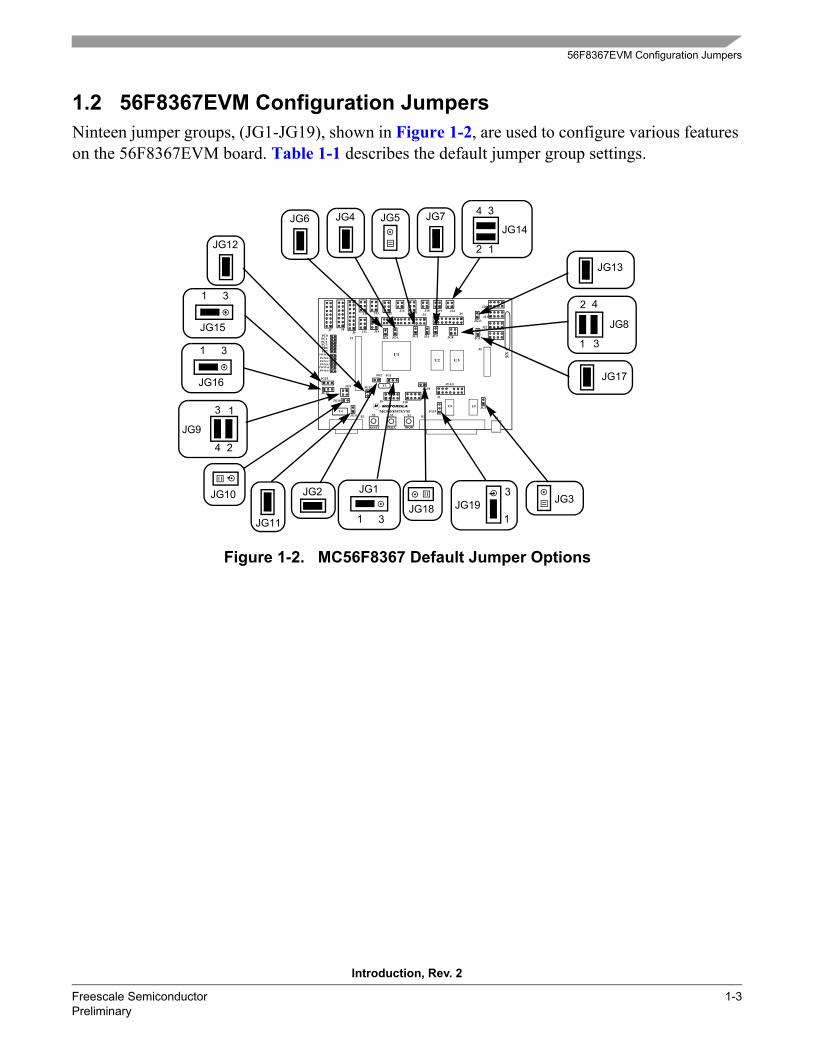
1.2 56F8367EVM Configuration JumpersNinteen jumper groups, (JG1-JG19), shown in Figure 1-2, are used to configure various features on the 56F8367EVM board. Table 1-1 describes the default jumper group settings.
MC56F8357EVMU4
J3
JTAG
P2
S/N
LED3
P1
Y1
U1U2
S2 S1S3P3
PC0
JG2
JG6
U8
RESET IRQBIRQA
1
2
JG9
JG18
JG3
JG1JG15
JG10
JG9
1
JG15
3
JG10
PC1PC2PC3PD6PD7
PWMA0PWMA1PWMA2PWMA3PWMA4PWMA5
U3
U9JG19
JG13
JG8
J20
J21
JG16
J10J9
J2
J1
J7 J8J6 J12 J14
J16J11 J13 J15
J19 J14
1JG19
3
1
JG16
3
3
4
1
JG1
3
JG2JG3
JG18
12
JG14
34JG5 JG7
JG11
JG12
JG6 JG4
1
2
JG8
3
4
JG17
JG13
J22
J23
J18J17
JG12
JG11
J5
JG4 JG5 J24 JG7
J4
JG17
Figure 1-2. MC56F8367 Default Jumper Options

Table 1-1. 56F8367EVM Default Jumper Options
JumperGroup Comment Jumpers
Connections
JG1 Use on-board EXTAL crystal input for oscillator 1–2
JG2 Use on-board XTAL crystal input for oscillator 1–2
JG3 Enable on-board Parallel JTAG Host/Target Interface NC
JG4 Enable Internal Boot Mode 1–2
JG5 Enable A0 - A23 for external memory accesses NC
JG6 Enable Crystal Mode 1–2
JG7 Enable SRAM Memory Bank 0 (use CS0) 1–2
JG8 Enable SRAM Memory Bank 1 (use CS1 & CS4) 1–2 & 3–4
JG9 Pass RXD0 & TXD0 to RS-232 level converter 1–2 & 3–4
JG10 Enable RS-232 output NC
JG11 Pass RS-232 RST to CTS 1–2
JG12 Pass Temperature Diode to ANA7 1–2
JG13 CAN #1 termination selected 1–2
JG14 Pass CAN2_TX & CAN2_RX to CAN tranceiver 1–2 & 3–4
JG15 High selected on User Jumper #0 1–2
JG16 High selected on User Jumper #1 1–2
JG17 CAN2 termination selected 1–2
JG18 Analog Ground to Digital Ground not reconnected NC
JG19 Use +3.3V for Printer Interface to on-board Parallel JTAG Host/Target 1-2
MC56F8367EVM User Manual, Rev. 2
1-4 Freescale Semiconductor Preliminary

56F8367EVM Connections
Introduction, Rev. 2
Freescale Semiconductor 1-5 Preliminary
1.3 56F8367EVM ConnectionsAn interconnection diagram is shown in Figure 1-3 for connecting the PC and the external +12.0V DC/AC power supply to the 56F8367EVM board.
PC-compatible
cable
computer
Parallel extension
MC56F8367EVM
External+12Vpower
P1
P3Connect cableto parallel / printer port
with 2.1mm,receptacleconnector
Figure 1-3. Connecting the 56F8367EVM Cables
Perform the following steps to connect the 56F8367EVM cables:
1. Connect the parallel extension cable to the parallel port of the host computer.
2. Connect the other end of the parallel extension cable to P1, shown in Figure 1-3, on the 56F8367EVM board. This provides the connection which allows the host computer to control the board.
3. Make sure that the external +12V DC, 1.2A power supply is not plugged into a +120V AC power source.
4. Connect the 2.1mm output power plug from the external power supply into P3, shown in Figure 1-3, on the 56F8367EVM board.
5. Apply power to the external power supply. The green Power-On LED, LED13, will illuminate when power is correctly applied.

MC56F8367EVM User Manual, Rev. 2
1-6 Freescale Semiconductor Preliminary

Technical Summary, Rev. 2
Freescale Semiconductor 2-1 Preliminary
Chapter 2 Technical SummaryThe 56F8367EVM is designed as a versatile development card using the 56F8367 processor, allowing the creation of real-time software and hardware products to support a new generation of applications in servo and motor control, digital and wireless messaging, digital answering machines, feature phones, modems, and digital cameras. The power of the 16-bit 56F8367 processor, combined with the on-board 128K x 16-bit external Program/Data Static RAM (SRAM), 128K x 16-bit external Data/Program SRAM, RS-232 interface, CAN interface, daughter card interface, peripheral expansion connectors and parallel JTAG interface, makes the 56F8367EVM ideal for developing and implementing many motor controlling algorithms, as well as for learning the architecture and instruction set of the 56F8367 processor.
The main features of the 56F8367EVM, with board and schematic reference designators, include:
• MC56F8367VPY60, a 16-bit +3.3V/+2.5V controller operating at 60MHz [U1]• External Fast Static RAM (FSRAM) memory, configured as:
— 128K x 16-bit of memory [U2] with 0 wait state at 60MHz via CS0— 128K x 16-bit of memory [U3] with 0 wait state at 60MHz via CS1/CS4
• 8.00MHz crystal oscillator, for base processor frequency generation [Y1]• Optional external oscillator frequency input connectors [JG1 and JG2]• Joint Test Action Group (JTAG) port interface connector, for an external debug Host
Target Interface [J3]• On-board parallel JTAG host target interface, with a connector for a PC printer port cable
[P1], including a disable jumper [JG3] and a printer port voltage selection jumper [JG19]• RS-232 interface, for easy connection to a host processor [U4 and P2], including a disable
jumper [JG10]• RTS and CTS RS-232 control signal access [JG11]• CAN interface, for high speed, 1.0Mbps, FlexCAN communications [U10 and J20]• CAN bypass and bus termination [J21 and JG13]

MC56F8367EVM User Manual, Rev. 2
2-2 Freescale Semiconductor Preliminary
• CAN #2 interface, for high speed, 1.0Mbps, FlexCAN communications [U11 and J22]• CAN #2 bypass and bus termination [J23 and JG17]• CAN #2 interface signal isolation [JG14]• Peripheral Daughter Card connector, to allow the user to connect his own SCI, SPI or
GPIO-compatible peripheral to the controller [J1]• Memory Daughter Card connector, to allow the user to connect his own memory or
memory device to the device [J2]• SCI #0 expansion connector, to allow the user to connect his own SCI #0 /
MPIO-compatible peripheral [J13]• SCI #1 expansion connector, to allow the user to connect his own SCI #1 /
MPIO-compatible peripheral [J14]• SPI #0 expansion connector, to allow the user to connect his own SPI #0 /
MPIO-compatible peripheral [J11]• SPI #1 expansion connector, to allow the user to connect his own SPI #1 /
MPIO-compatible peripheral [J12]• PWMA expansion connector, to allow the user to connect his own PWMA-compatible
peripheral [J7]• PWMB expansion connector, to allow the user to connect his own PWMB-compatible
peripheral [J8]• CAN #1 expansion connector, to allow the user to connect his own CAN physical layer
peripheral [J18]• CAN #2 expansion connector, to allow the user to connect his own CAN physical layer
peripheral [J19]• Timer A expansion connector, to allow the user to connect his own Timer A / Encoder
#0-compatible peripheral [J15]• Timer C expansion connector, to allow the user to connect his own Timer C-compatible
peripheral [J16]• Timer D expansion connector, to allow the user to connect his own Timer D-compatible
peripheral [J17]• ADC A expansion connector, to allow the user to attach his own A/D Port A-compatible
peripheral [J9]• ADC B expansion connector, to allow the user to attach his own A/D Port B-compatible
peripheral [J10]

Technical Summary, Rev. 2
Freescale Semiconductor 2-3 Preliminary
• Address bus expansion connector, to allow the user to monitor the external address bus [J4]
• Data bus expansion connector, to allow the user to monitor the external data bus [J5]• External memory bus control signal connector, to allow the user to monitor the external
memory bus [J6]• On-board power regulation provided from an external +12V DC-supplied power input
[P3]• Light Emitting Diode (LED) power indicator [LED13]• Six on-board real-time user debugging LEDs [LED1 - 6]• Six on-board Port A PWM monitoring LEDs [LED7 - 12]• Internal/external (EXTBOOT) boot mode selector [JG4]• Address range (EMI_MODE) boot mode selector [JG5]• Clock mode (CLKMODE) boot selector [JG6]• Temperature sense diode to ANA7 selector [JG12]• Manual reset push button [S1]• Manual interrupt push button for IRQA [S2]• Manual interrupt push button for IRQB [S3]• General-purpose jumper on GPIO PE4 [JG15]• General-purpose jumper on GPIO PE7 [JG16]

MC56F8367EVM User Manual, Rev. 2
2-4 Freescale Semiconductor Preliminary
2.1 MC56F8367The 56F8367EVM uses a Freescale MC56F8367VPY60 part, designated as U1 on the board and in the schematics. This part will operate at a maximum external bus speed of 60MHz. A full description of the 56F8367, including functionality and user information, is provided in these documents:
• 56F8367 Technical Data Sheet, (MC56F8367): Electrical and timing specifications, pin descriptions, device-specific peripheral information and package descriptions (this document)
• 56F8300 Peripheral User Manual, (MC56F8300UM): Detailed description of peripherals of the 56F8300 family of devices
• DSP56800E Reference Manual, (DSP56800ERM): Detailed description of the 56800E family architecture, 16-bit core processor, and the instruction set
Refer to these documents for detailed information about chip functionality and operation. They can be found on this URL:
www.freescale.com
2.2 Program and Data MemoryThe 56F8367EVM contains two 128K x 16-bit Fast Static RAM banks. SRAM bank 0 is controlled by CS0 and SRAM bank 1 is controlled by CS1 and CS4. This provides a total of 256K x 16 bits of external memory.

Program and Data Memory
Technical Summary, Rev. 2
Freescale Semiconductor 2-5 Preliminary
2.2.1 SRAM Bank 0SRAM bank 0, which is controlled by CS0, uses a 128K x 16-bit Fast Static RAM (GSI GS72116, labeled U2) for external memory expansion; see the FSRAM schematic diagram in Figure 2-1. CS0 can be configured to use this memory bank as 16 bits of Program memory, Data memory, or both. Additionally, CS0 can be configured to assign this memory’s size and starting address to any modulo address space.
This memory bank will operate with zero wait state access while the 56F8367 is running at 60MHz and can be disabled by removing the jumper at JG7.
MC56F8367 GS72116
A0 - A16
D0 - D15
RD
WR
A0 - A16
DQ0 - DQ15
OE
WE
CE
1 2
JG7
+3.3V
Jumper Pin 1-2:Enable SRAM
PS / CS0
Jumper Removed:Disable SRAM
Figure 2-1. Schematic Diagram of the External CS0 Memory Interface

MC56F8367EVM User Manual, Rev. 2
2-6 Freescale Semiconductor Preliminary
2.2.2 SRAM Bank 1SRAM bank 1, which is controlled by CS1 and CS2, uses a 128K x 16-bit Fast Static RAM (GSI GS72116, labeled U3) for external memory expansion; see the FSRAM schematic diagram in Figure 2-2. Using CS1 and CS4, this memory bank can be configured as byte (8-bit) or word (16-bit) accessable Program memory, Data memory, or both. Additionally, CS1 and CS4 can be configured to assign this memory’s size and starting address to any modulo address space.
This memory bank will operate with zero wait state access while the 56F8367 is running at 60MHz and can be disabled by removing the jumpers at JG8.
MC56F8367 GS72116
A0 - A16
D0 - D15
RD
WR
A0 - A16
DQ0 - DQ15
OE
WE
CE
JG8
Jumper Pin 1-2:Enable SRAM Low Byte
DS / CS1PD2 / CS4
LBHB
Jumper Pin 3-4:Enable SRAM High Byte
1
3
2
4
Figure 2-2. Schematic Diagram of the External CS1 / CS4 Memory Interface

RS-232 Serial Communications
Technical Summary, Rev. 2
Freescale Semiconductor 2-7 Preliminary
2.3 RS-232 Serial CommunicationsThe 56F8367EVM provides an RS-232 interface by the use of an RS-232 level converter, Maxim MAX3245EEAI, designated as U4. Refer to the RS-232 schematic diagram in Figure 2-3. The RS-232 level converter transitions the SCI port’s +3.3V signal levels to RS-232-compatible signal levels and connects to the host’s serial port via connector P2. RTS/CTS flow control is provided on JG11 as a jumper, but could be implemented using uncommitted GPIO signals. The SCI port #0 signals can be isolated from the RS-232 level converter by removing the jumpers in JG9; see Table 2-1. The pin-out of connector P2 is listed in Table 2-2. The RS-232 level converter/transceiver can be disabled by placing a jumper at JG10.
MC56F8367RS-232
Level Converter Interface
TXD0
RXD0 R1 in
T1 outT1 in
R1 out
FORCEOFF
JG10
6
3
27
84
5x
1
9
+3.3V
Jumper Removed:Enable RS-232
P2
JG91 2
3 4
12Jumper Pin 1-2:
Disable RS-232
R2 in
T2 out
JG11
1
2
T2 in
R2 out
RTS
CTS
TXD
RXD
Figure 2-3. Schematic Diagram of the RS-232 Interface
Table 2-1. SCI #0 Jumper Options
JG9
Pin # Signal Pin # Signal
1 TXD0 2 RS-232 TXD
3 RXD0 4 RS-232 RXD

Table 2-2. RS-232 Serial Connector Description
P2
Pin # Signal Pin # Signal
1 Jumper to 6 & 4 6 Jumper to 1 & 4
2 TXD 7 CTS
3 RXD 8 RTS
4 Jumper to 1 & 6 9 NC
5 GND
MC56F8367EVM User Manual, Rev. 2
2-8 Freescale Semiconductor Preliminary
2.4 Clock SourceThe 56F8367EVM uses an 8.00MHz crystal, Y1, connected to its external crystal inputs, EXTAL and XTAL. To achieve its maximum internal operating frequency, the 56F8367 uses its internal PLL to multiply the input frequency. An external oscillator source can be connected to the processor by using the oscillator bypass connectors, JG1 and JG2; see Figure 2-4. If the input frequency is above 8MHz, then the EXTAL input should be jumpered to ground by adding a jumper between JG1 pins 2 and 3. The input frequency would then be injected on JG2’s pin 2. If the input frequency is below 4MHz, then the input frequency can be injected on JG1’s pin 2.
MC56F8367
ExternalOscillatorHeaders
JG11 23
1 2
EXTAL
XTAL
JG2
8.00MHz
Figure 2-4. Schematic Diagram of the Clock Interface

Operating Mode
Technical Summary, Rev. 2
Freescale Semiconductor 2-9 Preliminary
2.5 Operating ModeThe 56F8367EVM provides three boot mode selection jumpers, EXTBOOT, EMI_MODE and CLKMODE, to provide boot-up mode options.
2.5.1 EXTBOOTThe 56F8367EVM provides an external/internal boot mode jumper, JG4. This jumper is used to select the internal or external memory operation of the processor as it exits reset. Refer to the 56F8300 Peripheral User Manual and the 56F8367 Technical Data Sheet for a complete description of the chip’s operating modes. Table 2-3 shows the two external boot operation modes available on the 56F8367.
Table 2-3. EXTBOOT Operating Mode Selection
Operating Mode JG4 Comment
0 1 - 2 Bootstrap from internal memory (GND)
3 No Jumper Bootstrap from external memory (+3.3V)
2.5.2 EMI_MODEThe 56F8367EVM provides an EMI boot mode jumper, JG5. This jumper is used to select the external memory addressing range operating mode of the processor as it exits reset. The user can select between a 64K address space or an 8M address space. Refer to the 56F8300 Peripheral User Manual and the 56F8367 Technical Data Sheet for a complete description of the chip’s operating modes. Table 2-4 shows the two EMI operation modes available on the 56F8367.
Table 2-4. EMI Operating Mode Selection
Operating Mode JG5 Comment
V1 1 - 2 A0 - A15 (64K) available for external memory bus (GND)
V2 No Jumper A0 - A23 (8M) available for external memory bus (+3.3V)

MC56F8367EVM User Manual, Rev. 2
2-10 Freescale Semiconductor Preliminary
2.5.3 CLKMODEThe 56F8367EVM provides a clock boot mode jumper, JG6. This jumper is used to select the type of clock source being provided to the processor as it exits reset. The user can select between the use of a crystal or an oscillator as the clock source for the processor. Refer to the 56F8300 Peripheral User Manual and the 56F8367 Technical Data Sheet for a complete description of the chip’s operating modes. Table 2-5 shows the two CLKMODE operation modes available on the 56F8367.
Table 2-5. EMI Operating Mode Selection
Operating Mode JG6 Comment
Crystal 1 - 2 Enables the external clock drive logic so an external crystal can be used as the input clock source. (GND)
Oscillator No Jumper Disables the external clock drive logic. Use oscillator input on XTAL and Ground on EXTAL. (3.3V)
2.6 Debug LEDsSix on-board Light Emitting Diodes, (LEDs), are provided to allow real-time debugging for user programs. These LEDs will allow the programmer to monitor program execution without having to stop the program during debugging; refer to Figure 2-5. Table 2-6 describes the control of each LED.
Table 2-6. LED Control
Controlled by
User LED Color Signal
LED1 RED Port C Bit 0 (PC0)
LED2 YELLOW Port C Bit 1 (PC1)
LED3 GREEN Port C Bit 2 (PC2)
LED4 RED Port C Bit 3 (PC3)
LED5 YELLOW Port D Bit 6 (PD6)
LED6 GREEN Port D Bit 7 (PD7)

Debug Support
Technical Summary, Rev. 2
Freescale Semiconductor 2-11 Preliminary
Setting PC0, PC1, PC2, PC3, PD6, or PD7 to a Logic One value will turn on the associated LED.
MC56F8367 INVERTING BUFFER
PC0
PC1
PC2GREEN LED
YELLOW LED
RED LED+3.3V
GREEN LED
YELLOW LED
RED LED
PC3
PD6
PD7
Figure 2-5. Schematic Diagram of the Debug LED Interface
2.7 Debug SupportThe 56F8367EVM provides an on-board parallel JTAG host target interface and a JTAG interface connector for external target interface support. Two interface connectors are provided to support each of these debugging approaches. These two connectors are designated the JTAG connector and the host parallel interface connector.

MC56F8367EVM User Manual, Rev. 2
2-12 Freescale Semiconductor Preliminary
2.7.1 JTAG ConnectorThe JTAG connector on the 56F8367EVM allows the connection of an external host target interface for downloading programs and working with the 56F8367’s registers. This connector is used to communicate with an external host target interface, which passes information and data back and forth with a host processor running a debugger program. Table 2-7 shows the pin-out for this connector.
Table 2-7. JTAG Connector Description
J3
Pin # Signal Pin # Signal
1 TDI 2 GND
3 TDO 4 GND
5 TCK 6 GND
7 NC 8 KEY
9 RESET 10 TMS
11 +3.3V 12 NC
13 DE 14 TRST
When this connector is used with an external host target interface, the parallel JTAG interface should be disabled by placing a jumper in jumper block JG3. Reference Table 2-8 for this jumper’s selection options.
Table 2-8. Parallel JTAG Interface Disable Jumper Selection
JG3 Comment
No jumpers Enables On-board Parallel JTAG Interface
1 - 2 Disables on-board Parallel JTAG Interface

Debug Support
Technical Summary, Rev. 2
Freescale Semiconductor 2-13 Preliminary
2.7.2 Parallel JTAG Interface ConnectorThe Parallel JTAG Interface Connector, P1, allows the 56F8367 to communicate with a parallel printer port on a Windows PC; reference Figure 2-6. Using this connector, the user can download programs and work with the 56F8367’s registers. Table 2-9 shows the pin-out for this connector. When using the parallel JTAG interface, the jumper at JG3 should be removed, as shown in Table 2-8. The printer port interface voltage of +3.3V or +5.0V can be selected by a jumper on JG19, as shown in Table 2-10.
DB-25 Connector Parallel JTAG Interface MC56F8367
TDITDO
P_TRSTTMSTCK
P_RESET
OUTOUT
OUT
OUTOUT
OUTIN
ININ
IN
ININ
EN
TDITDOTRST
TMSTCK
RESET
JG312
+3.3V
Jumper Removed:Enable JTAG I/F
Jumper Pin 1-2:Disable JTAG I/F
P_DE OUTIN DE
JG1912 3
Vcc
+3.3V
+5.0V
Figure 2-6. Block Diagram of the Parallel JTAG Interface

Table 2-9. Parallel JTAG Interface Connector Description
P1
Pin # Signal Pin # Signal
1 NC 14 NC
2 PORT_RESET 15 PORT_IDENT
3 PORT_TMS 16 NC
4 PORT_TCK 17 NC
5 PORT_TDI 18 GND
6 PORT_TRST 19 GND
7 PORT_DE 20 GND
8 PORT_IDENT 21 GND
9 PORT_VCC 22 GND
10 NC 23 GND
11 PORT_TDO 24 GND
12 NC 25 GND
13 PORT_CONNECT
Table 2-10. Parallel JTAG Interface Voltage Jumper Selection
JG19 Comment
1 - 2 Interface with the PC’s printer port using +3.3V signals
2 - 3 Interface with the PC’s printer port using +5.0V signals
MC56F8367EVM User Manual, Rev. 2
2-14 Freescale Semiconductor Preliminary
External Interrupts
Technical Summary, Rev. 2
Freescale Semiconductor 2-15 Preliminary
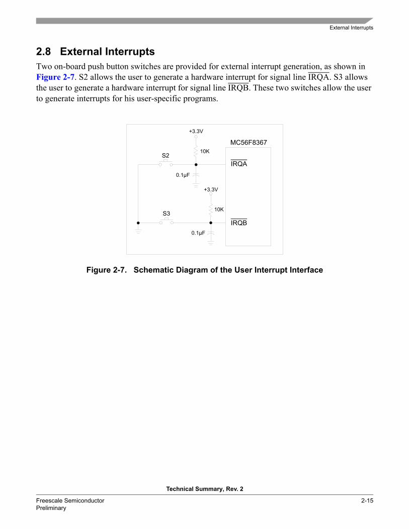
2.8 External InterruptsTwo on-board push button switches are provided for external interrupt generation, as shown in Figure 2-7. S2 allows the user to generate a hardware interrupt for signal line IRQA. S3 allows the user to generate a hardware interrupt for signal line IRQB. These two switches allow the user to generate interrupts for his user-specific programs.
MC56F8367
IRQA
IRQB
+3.3V
+3.3V
10K
10K
S2
S3
0.1µF
0.1µF
Figure 2-7. Schematic Diagram of the User Interrupt Interface

MC56F8367EVM User Manual, Rev. 2
2-16 Freescale Semiconductor Preliminary
2.9 ResetLogic is provided on the 56F8367 to generate an internal power-on reset. Additional reset logic is provided to support the reset signals from the JTAG connector, the parallel JTAG interface and the user reset push button, S1; refer to Figure 2-8.
RESETPUSHBUTTON
MANUAL RESET
JTAG_TAP_RESET
JTAG_RESETRESET
TRST
S1
Figure 2-8. Schematic Diagram of the Reset Interface

Power Supply
Technical Summary, Rev. 2
Freescale Semiconductor 2-17 Preliminary
2.10 Power SupplyThe main power input to the 56F8367EVM, +12V DC at 1.2A, is through a 2.1mm coax power jack. This input power is rectified to provide a DC supply input. This allows a user the option to use a +12V AC power supply. A 1.2 Amp power supply is provided with the 56F8367EVM; however, less than 500mA is required by the EVM. The remaining current is available for custom control applications when connected to the daughter card connectors. The 56F8367EVM provides +5.0V DC regulation for the CAN interface and additional regulators. The 56F8367EVM provides +3.3V DC voltage regulation for the processor, memory, D/A, ADC, parallel JTAG interface and supporting logic; refer to Figure 2-9. Additional voltage regulation logic provides a low-noise +3.3V DC voltage reference to the processor’s A/D VREFH. A jumper, JG18, and resistor, R66, are provided to allow the analog and digital grounds to be isolated on the 56F8367EVM board. This allows the analog ground reference point to be provided on a custom board attached to the 56F8367EVM daughter card connectors. By removing R66, the AGND reference is disconnected from the 56F8367EVM’s digital ground. By placing a jumper on JG18, the AGND is reconnected to the 56F8367EVM’s digital ground. Power applied to the 56F8367EVM is indicated with a power-on LED, referenced as LED13. Optionally, the user can provide the +2.5 DC voltage needed by the processor’s core on connector J24 and disable the on-chip core voltage regulator by moving the resistor at R72 to R71. Additonally, four zero ohm resistors or shorting wires must be added at R67, R68, R69, and R70 to allow the external +2.5V DC to pass to the 56F8367.
+5.0V DC+12V DC/AC PowerCondition
CAN
56F8367VDD_IO & PLL
+3.3VRegulator
P3
56F8367EVMParts
56F8367VREFH
+3.3V DC
+3.3VA DC
+5.0VRegulator
56F8367 ADC
+3.3VRegulator
+3.3VA DC
56F8367VDD Core
+2.5V DCExt In
1
2
J24
U15
R67 - R70
BridgeRectifier
Input
+3.3VRegulator
Power On
Figure 2-9. Schematic Diagram of the Power Supply

MC56F8367EVM User Manual, Rev. 2
2-18 Freescale Semiconductor Preliminary
2.11 Daughter Card ConnectorsThe EVM board contains two daughter card connectors. One connector, J1, contains the processor’s peripheral port signals. The second connector, J2, contains the processor’s external memory bus signals.
2.11.1 Peripheral Daughter Card ConnectorThe processor’s peripheral port signals are connected to the peripheral daughter card connector, J1. The peripheral daughter card connector is used to connect a daughter card or a user-specific daughter card to the processor’s peripheral port signals. The peripheral port daughter card connector is a 100-pin high-density connector with signals for the IRQs, reset, SPI, SCI, PWM, ADC and Quad Timer ports. Table 2-11 shows the peripheral daughter card connector’s signal-to-pin assignments.
Table 2-11. Peripheral Daughter Card Connector Description
J1
Pin # Signal Pin # Signal
1 +12V 2 +12V
3 GND 4 GND
5 +5.0V 6 +5.0V
7 GND 8 GND
9 +3.3V 10 +3.3V
11 GND 12 GND
13 PHASEA0 / TA0 / PC4 14 PHASEB0 / TA1 / PC5
15 INDEX0 / TA2 / PC6 16 HOME0 / TA3 / PC7
17 GND 18 GND
19 PHASEA1 / PC0 / TB0 / SCLK1 20 PHASEB1 / PC1 / TB1 / MOSI1
21 INDEX1 / PC2 / TB2 / MISO1 22 HOME1 / PC3 / TB3 / SS1
23 TXD0 / PE0 24 TXD1 / PD6
25 TXD0 / PE0 26 TXD1 / PD6
27 RXD0 / PE1 28 RXD1 / PD7

Daughter Card Connectors
Technical Summary, Rev. 2
Freescale Semiconductor 2-19 Preliminary
29 IRQA 30 IRQB
31 RXD0 / PE1 32 RXD1 / PD7
33 PWMB0 34 PWMB1
35 PWMB2 36 PWMB3
37 PWMB4 38 PWMB5
39 GND 40 GND
41 ISB0 / PD10 42 ISB1 / PD11
43 ISB2 / PD12 44 GND
45 FAULTB1 46 FAULTB0
47 FAULTB3 48 FAULTB2
49 GND 50 GND
51 PWMA0 52 PWMA1
53 PWMA2 54 PWMA3
55 PWMA4 56 PWMA5
57 GND 58 GND
59 FAULTA0 60 FAULTA1
61 FAULTA2 62 MISO0 / PE6
63 ISA0 / PC8 64 ISA1 / PC9
65 ISA2 / PC10 66 RSTO
67 MOSI0 / PE5 68 SS0 / PE7
69 TD0 / PE10 70 TD1 / PE11
71 SCLK0 / PE7 72 TC0 / PE8
73 CAN_TX 74 CAN_RX
75 MOSI0 / PE5 76 MISO0 / PE6
77 SCLK0 / PE4 78 SS0 / PE7
79 GND 80 GND
Table 2-11. Peripheral Daughter Card Connector Description (Continued)
J1
Pin # Signal Pin # Signal

MC56F8367EVM User Manual, Rev. 2
2-20 Freescale Semiconductor Preliminary
2.11.2 Memory Daughter Card ConnectorThe processor’s external memory bus signals are connected to the memory daughter card connector, J2. Table 2-12 shows the port signal-to-pin assignments.
81 +VREFH 82 +VREFH
83 GNDA 84 GNDA
85 AN0 86 AN1
87 AN2 88 AN3
89 AN4 90 AN5
91 AN6 92 AN7
93 AN8 94 AN9
95 AN10 96 AN11
97 AN12 98 AN13
99 AN14 100 AN15
Table 2-12. Memory Daughter Card Connector Description
J2
Pin # Signal Pin # Signal
1 A4 / PA12 2 A5 / PA13
3 A3 / PA11 4 A6 / PE2
5 A2 / PA10 6 A7 / PE3
7 A1 / PA9 8 RD
9 GND 10 GND
11 A0 / PA8 12 DS / CS1
13 PS / CS0 14 PD0 / CS2 / CAN2_TX
Table 2-11. Peripheral Daughter Card Connector Description (Continued)
J1
Pin # Signal Pin # Signal

Daughter Card Connectors
Technical Summary, Rev. 2
Freescale Semiconductor 2-21 Preliminary
15 D0 / PF9 16 D15 / PF8
17 D1 / PF10 18 D14 / PF7
19 GND 20 GND
21 GND 22 GND
23 D2 / PF11 24 D13 / PF6
25 D3 / PF12 26 D12 / PF5
27 D4 / PF13 28 D11 / PF4
29 D5 / PF14 30 D10 / PF3
31 GND 32 GND
33 GND 34 GND
35 D6 / PF15 36 D9 / PF2
37 D7 / PF0 38 D8 / PF1
39 WR 40 PD1 / CS3 / CAN2_RX
41 A15 / PA7 42 A8 / PA0
43 GND 44 GND
45 A14 / PA6 46 A9 / PA1
47 A13 / PA5 48 A10 / PA2
49 A12 / PA4 50 A11 / PA3
51 PB0 / A16 52 GND
53 GND 54 GND
55 +3.3V 56 +3.3V
57 GND 58 GND
59 +5.0V 60 +5.0V
Table 2-12. Memory Daughter Card Connector Description (Continued)
J2
Pin # Signal Pin # Signal

MC56F8367EVM User Manual, Rev. 2
2-22 Freescale Semiconductor Preliminary
2.12 Motor Control PWM Signals and LEDsThe 56F8367 has two independent groups of dedicated PWM units. Each unit contains six PWM, three phase current sense inputs and four fault input lines. PWM group A’s PWM lines are connected to a set of six PWM LEDs via inverting buffers. The buffers are used to isolate and drive the Processor’s PWM group A’s outputs to the PWM LEDs. The PWM LEDs indicate the status of PWM group A signals; refer to Figure 2-10. PWM Group A and B signals are routed out to headers, J7 and J8 respectively, and to the peripheral daughter card connector for easy use by the end user.
LED
+3.3V
LED9
56F8367
LED10
LED11
LED12
LED7
LED8
PWMA0PWMA1
PWMA2PWMA3
PWMA5
Buffer
PWMA0
Yellow LED
PWMA1
PWMA2PWMA3PWMA4PWMA5
Green LED
Yellow LED
Green LED
Yellow LED
Green LED
Phase A Top
Phase A Bottom
Phase B Top
Phase B Bottom
Phase C Top
Phase C Bottom
PWMA4
Figure 2-10. PWM Group A Interface and LEDs

CAN Interfaces
Technical Summary, Rev. 2
Freescale Semiconductor 2-23 Preliminary
2.13 CAN InterfacesThe 56F8367EVM board contains two FlexCAN interfaces. The primary CAN interface uses the CAN1_RX and CAN1_TX pins on the 56F8367. The secondary CAN interface uses the CAN2_RX and CAN2_TX pins on the 56F8367.
2.13.1 FlexCAN #1 InterfaceThe 56F8367EVM board contains a CAN physical-layer interface chip that is attached to the FlexCAN port’s CAN1_RX and CAN1_TX pins on the 56F8367. The EVM board uses a Phillips high-speed, 1.0Mbps, physical layer interface chip, PCA82C250. Due to the +5.0V operating voltage of the CAN interface chip, a pull-up to +5.0V is required to level shift the transmit data output line from the 56F8367. The CANH and CANL signals pass through inductors before attaching to the CAN bus connectors. A primary, J20, and daisy-chain, J21, CAN connector are provided to allow easy daisy-chaining of CAN devices. CAN bus termination of 120 ohms can be provided by adding a jumper to JG13. Refer to Table 2-14 for the CAN connector signals and Figure 2-12 for a connection diagram.
MC56F8367
+5.0V
CAN Transceiver
J20
Daisy-Chain CAN #1Connector
J21
CAN #1 BusConnector
CAN Bus #1Terminator
JG13
120
PCA82C250
1K
CAN1_TX
CAN1_RX
1
2
3
45
4
35
CANH
CANL
TXD
RXD
Figure 2-11. CAN #1 Interface
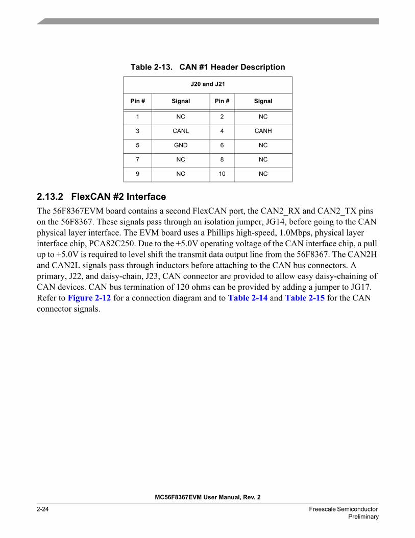
Table 2-13. CAN #1 Header Description
J20 and J21
Pin # Signal Pin # Signal
1 NC 2 NC
3 CANL 4 CANH
5 GND 6 NC
7 NC 8 NC
9 NC 10 NC
MC56F8367EVM User Manual, Rev. 2
2-24 Freescale Semiconductor Preliminary
2.13.2 FlexCAN #2 InterfaceThe 56F8367EVM board contains a second FlexCAN port, the CAN2_RX and CAN2_TX pins on the 56F8367. These signals pass through an isolation jumper, JG14, before going to the CAN physical layer interface. The EVM board uses a Phillips high-speed, 1.0Mbps, physical layer interface chip, PCA82C250. Due to the +5.0V operating voltage of the CAN interface chip, a pull up to +5.0V is required to level shift the transmit data output line from the 56F8367. The CAN2H and CAN2L signals pass through inductors before attaching to the CAN bus connectors. A primary, J22, and daisy-chain, J23, CAN connector are provided to allow easy daisy-chaining of CAN devices. CAN bus termination of 120 ohms can be provided by adding a jumper to JG17. Refer to Figure 2-12 for a connection diagram and to Table 2-14 and Table 2-15 for the CAN connector signals.

MC56F8367
+5.0V
CAN Transceiver
J22
Daisy-Chain CAN #2
Connector
J23
CAN #2 BusConnector
CAN #2 BusTerminator
JG17
120
PCA82C250
1K
PD0 / CAN2_TX
PD1 / CAN2_RX
1
2
3
45
4
35
CANH
CANL
TXD
RXD
1
3 4
2JG14
CAN Interfaces
Technical Summary, Rev. 2
Freescale Semiconductor 2-25 Preliminary
Figure 2-12. CAN #2 Interface
Table 2-14. CAN #2 Header Description
J22 and J23
Pin # Signal Pin # Signal
1 NC 2 NC
3 CAN2L 4 CAN2H
5 GND 6 NC
7 NC 8 NC
9 NC 10 NC
Table 2-15. CAN #2 Pass-Through Jumper Description
JG14
Pin # Signal Pin # Signal
1 PD0 2 CAN2_TX
3 PD1 4 CAN2_RX

MC56F8367EVM User Manual, Rev. 2
2-26 Freescale Semiconductor Preliminary
2.14 Software Feature JumpersThe 56F8367EVM board contains two software feature jumpers that allow the user to select user-defined software features. Two GPIO port pins, PE4 and PE7, are pulled high or low with 10K ohm resistors on JG15 and JG16. Attaching a jumper between pins 1 and 2 will place a high or 1 on the port pin. Attaching a jumper between pins 2 and 3 will place a low or 0 on the port pin; see Figure 2-13.
MC56F8367JG15
User Jumper#0SCLK0 / PE4
SS0 / PE7
12
3
10K+3.3V
JG16User Jumper
#11
23
10K
10K
+3.3V
10K
Figure 2-13. Software Feature Jumpers

Peripheral Expansion Connectors
Technical Summary, Rev. 2
Freescale Semiconductor 2-27 Preliminary
2.15 Peripheral Expansion ConnectorsThe EVM board contains a group of peripheral expansion connectors used to gain access to the resources of the 56F8367. The following signal groups have expansion connectors:
• External Memory Address Bus (A0 - A23) General Purpose Port A (bits 0 - 13) General Purpose Port E (bits 2 & 3) General Purpose Port B (bit 0 - 7)
• External Memory Data Bus (D0 - D15) General Purpose Port F (bits 0 - 15)
• External Memory Control General Purpose Port D (bits 0 - 5, 8 & 9)
• Quadrature Decoder #0 Quad Timer Channel A
• Quadrature Decoder #1 Serial Peripheral Interface Port #1 Quad Timer Channel B General Purpose Port C (bits 0 - 3)
• Quad Timer Channel C General Purpose Port E (bits 8 & 9)
• Quad Timer Channel D General Purpose Port E (bits 10 - 13)
• A/D Input Port A• A/D Input Port B• Serial Communications Port #0 / General Purpose Port E (bits 0 and 1)• Serial Communications Port #1 / General Purpose Port D (bits 6 and 7)• Serial Peripheral Interface Port #0 / General Purpose Port E (bits 4 - 7)• PWM Port A / General Purpose Port C (bits 8 - 10)• PWM Port B / General Purpose Port C (bits 0 - 3)• CAN Port #1• CAN Port #2

MC56F8367EVM User Manual, Rev. 2
2-28 Freescale Semiconductor Preliminary
2.15.1 Address Bus Expansion ConnectorThe address bus expansion connector contains the 56F8367’s 24 external memory address signal lines. Address lines A6 and A7 can optionally be used as GPIO Port E lines (bits 2 and 3). Address lines A8 - A15 can optionally be used as GPIO Port A lines (bits 0 - 7). Address lines A0 - A5 can optionally be used as GPIO Port A lines (bits 8 - 13). Address lines A16 - A23 are MPIO signals, which can be configured as A16 - A23 or GPIO Port B bits 0 - 7. Refer to Table 2-16 for the address bus connector information.
Table 2-16. External Memory Address Bus Connector Description
J4
Pin # Signal Pin # Signal
1 A0 / PA8 2 A1 / PA9
3 A2 / PA10 4 A3 / PA11
5 A4 / PA12 6 A5 / PA13
7 A6 / PE2 8 A7 / PE3
9 A8 / PA0 10 A9 / PA1
11 A10 / PA2 12 A11 / PA3
13 A12 / PA4 14 A13 / PA5
15 A14 / PA6 16 A15 / PA7
17 PB0 / A16 18 PB1 / A17
19 PB2 / A18 20 PB3 / A19
21 PB4 / A20 22 PB5 / A21
23 PB6 / A22 24 PB7 / A23
19 GND 20 +3.3V

Peripheral Expansion Connectors
Technical Summary, Rev. 2
Freescale Semiconductor 2-29 Preliminary
2.15.2 Data Bus Expansion ConnectorThe data bus expansion connector contains the 56F8367’s 16 external memory data signal lines. Refer to Table 2-17 for the data bus connector information. Data lines D0 - D15 can also be used as GPIO Port F lines (bits 0 - 15).
Table 2-17. External Memory Address Bus Connector Description
J5
Pin # Signal Pin # Signal
1 D0 / PF9 2 D1 / PF10
3 D2 / PF11 4 D3 / PF12
5 D4 / PF13 6 D5 / PF14
7 D6 / PF15 8 D7 / PF0
9 D8 / PF1 10 D9 / PF2
11 D10 / PF3 12 D11 / PF4
13 D12 / PF5 14 D13 / PF6
15 D14 / PF7 16 D15 / PF8
17 GND 18 +3.3V

MC56F8367EVM User Manual, Rev. 2
2-30 Freescale Semiconductor Preliminary
2.15.3 External Memory Control Signal Expansion ConnectorThe external memory control signal connector contains the 56F8367’s external memory control signal lines. CS2 and CS3 are MPIO signals, which can be configured as GPIO Port D lines (bits 0 and 1). Refer to Table 2-18 for the names of these signals.
Table 2-18. External Memory Control Signal Connector Description
J6
Pin # Signal Pin # Signal
1 RD 2 IRQA
3 WR 4 IRQB
5 PS / CS0 6 DS / CS1
7 PD0 / CS2 / CAN2_TX 8 PD1 / CS3 / CAN2_RX
PD2 / CS4 PD3 / CS5
PD4 / CS6 PD5 / CS7
9 CLKO 10 RESET
11 GND 12 RSTO
2.15.4 Encoder #0 / Quad Timer Channel A Expansion ConnectorThe Encoder #0 / Quad Timer Channel A port is an MPIO port attached to the Timer A expansion connector. This port can be configured as a Quadrature Decoder interface port or as a Quad Timer port. Refer to Table 2-19 for the signals attached to the connector.
Table 2-19. Timer A Signal Connector Description
J15
Pin # Signal Pin # Signal
1 PHASEA0 / TA0 2 PHASEB0 / TA1
3 INDEX0 / TA2 4 HOME0 / TA3
5 GND 6 +3.3V

Peripheral Expansion Connectors
Technical Summary, Rev. 2
Freescale Semiconductor 2-31 Preliminary
2.15.5 Encoder #1 / SPI #1 Expansion ConnectorThe Encoder #1 / SPI #1 port is an MPIO port attached to the SPI #1 expansion connector. This port can be configured as a Quadrature Decoder interface port, a Serial Peripherial Interface, Quad Timer port or General Purpose I/O port. Refer to Table 2-20 for the signals attached to the connector.
Table 2-20. SPI #1 Signal Connector Description
J12
Pin # Signal Pin # Signal
1 PHASEB1 / MOSI1 / TB1 / PC1 2 INDEX1 / MISO1 / TB2 / PC2
3 PHASEA1 / SCLK1 / TB0 / PC0 4 HOME1 / SS1 / TB3 / PC3
5 GND 6 +3.3V
2.15.6 Timer Channel C Expansion ConnectorThe Timer Channel C port is a Quad Timer port attached to the Timer C expansion connector. This port can be configured as a Quad Timer port or a General Purpose I/O port. Refer to Table 2-21 for the signals attached to the connector.
Table 2-21. Timer Channel C Connector Description
J16
Pin # Signal Pin # Signal
1 TC0 / PE8 2 TC1 / PE9
3 GND 4 +3.3V

MC56F8367EVM User Manual, Rev. 2
2-32 Freescale Semiconductor Preliminary
2.15.7 Timer Channel D Expansion ConnectorThe Timer Channel D port is a Quad Timer attached to the Timer D expansion connector. This port can be configured as a Quad Timer port or a General Purpose I/O port. Refer to Table 2-22 for the signals attached to the connector.
Table 2-22. Timer Channel D Connector Description
J17
Pin # Signal Pin # Signal
1 TD0 / PE10 2 TD1 / PE11
3 TD2 / PE12 4 TD3 / PE13
3 GND 4 +3.3V

Peripheral Expansion Connectors
Technical Summary, Rev. 2
Freescale Semiconductor 2-33 Preliminary
2.15.8 A/D Port A Expansion ConnectorThe eight-channel Analog-to-Digital conversion Port A is attached to this connector. Refer to Table 2-23 for connection information. There is a Resistor/Connector (R/C) network on each of the Analog Port A input signals; see Figure 2-14.
Table 2-23. A/D Port A Connector Description
J9
Pin # Signal Pin # Signal
1 AN0 2 AN1
3 AN2 4 AN3
5 AN4 6 AN5
7 AN6 8 AN7
9 GNDA 10 +VREFH
To Processor’s Analog Port
100 ohmAnalog Input
0.0022uF
Figure 2-14. Typical Analog Input RC Filter

MC56F8367EVM User Manual, Rev. 2
2-34 Freescale Semiconductor Preliminary
2.15.9 A/D Port B Expansion ConnectorThe eight-channel Analog-to-Digital conversion Port B is attached to this connector. Refer to Table 2-24 for connection information. There is an R/C network on each of the Analog Port B input signals; see Figure 2-14.
Table 2-24. A/D Port B Connector Description
J10
Pin # Signal Pin # Signal
1 AN8 2 AN9
3 AN10 4 AN11
5 AN12 6 AN13
7 AN14 8 AN15
9 GNDA 10 +VREFH
2.15.10 Serial Communications Port #0 Expansion ConnectorThe Serial Communications Port #0 is an MPIO port attached to the SCI #0 expansion connector. This port can be configured as a Serial Communications Interface or as a General Purpose I/O port. Refer to Table 2-25 for connection information.
Table 2-25. SCI #0 Connector Description
J13
Pin # Signal Pin # Signal
1 TXD0 / PE0 2 RXD0 / PE1
3 GND 4 +3.3V
5 GND 6 +5.0V

Peripheral Expansion Connectors
Technical Summary, Rev. 2
Freescale Semiconductor 2-35 Preliminary
2.15.11 Serial Communications Port #1 Expansion ConnectorThe Serial Communications Port #1 is an MPIO port attached to the SCI #1 expansion connector. This port can be configured as a Serial Communications Interface or as a General Purpose I/O port. Refer to Table 2-26 for connection information.
Table 2-26. SCI #1 Connector Description
J14
Pin # Signal Pin # Signal
1 TXD1 / PD6 2 RXD1 / PD7
3 GND 4 +3.3V
5 GND 6 +5.0V
2.15.12 Serial Peripheral Interface #0 Expansion ConnectorThe Serial Peripheral Interface #0 is an MPIO port attached to this connector. This port can be configured as a Serial Peripheral Interface or as a General Purpose I/O port. Refer to Table 2-27 for the connection information.
Table 2-27. SPI #0 Connector Description
J11
Pin # Signal Pin # Signal
1 MOSI0 / PE5 2 MISO0 / PE6
3 SCLK0 / PE4 4 SS0 / PE7
5 GND 6 +3.3V

MC56F8367EVM User Manual, Rev. 2
2-36 Freescale Semiconductor Preliminary
2.15.13 FlexCAN #1 Expansion ConnectorThe FlexCAN Port #1 is attached to this connector. Refer to Table 2-28 for connection information.
Table 2-28. CAN #1 Connector Description
J18
Pin # Signal Pin # Signal
1 CAN1_TX 2 GND
3 CAN1_RX 4 GND
2.15.14 FlexCAN #2 Expansion ConnectorThe FlexCAN Port #2 is attached to this connector. Refer to Table 2-29 for connection information.
Table 2-29. CAN #2 Connector Description
J19
Pin # Signal Pin # Signal
1 CAN2_TX 2 GND
3 CAN2_RX 4 GND

Peripheral Expansion Connectors
Technical Summary, Rev. 2
Freescale Semiconductor 2-37 Preliminary
2.15.15 PWM Port A Expansion ConnectorThe PWM Port A is attached to this connector. Refer to Table 2-30 for connection information.
Table 2-30. PWM Port A Connector Description
J7
Pin # Signal Pin # Signal
1 PWMA0 2 PWMA1
3 PWMA2 4 PWMA3
5 PWMA4 6 PWMA5
7 FAULTA0 8 FAULTA1
9 FAULTA2 10 FAULTA3
11 ISA0 / PC8 12 ISA1 / PC9
13 ISA2 / PC10 14 GND
2.15.16 PWM Port B Expansion ConnectorThe PWM Port B is attached to this connector. Refer to Table 2-31 for connection information.
Table 2-31. PWM Port B Connector Description
J8
Pin # Signal Pin # Signal
1 PWMB0 2 PWMB1
3 PWMB2 4 PWMB3
5 PWMB4 6 PWMB5
7 FAULTB0 8 FAULTB1
9 FAULTB2 10 FAULTB3
11 ISB0 / PD10 12 ISB1 / PD11
13 ISB2 / PD12 14 GND

MC56F8367EVM User Manual, Rev. 2
2-38 Freescale Semiconductor Preliminary
2.16 Test PointsThe 56F8367EVM board has a total of seven test points:
• Analog Ground (AGND)• Three Digital Grounds (GND)• +3.3V• +3.3VA• +5.0V

56F8367EVM Schematics, Rev. 2
Freescale Semiconductor Appendix A-1 Preliminary
Appendix A 56F8367EVM Schematics

A A
B B
C C
D D
E E
44
33
22
11
Single trace
to GNDA
Use on-chip
regulators
Single trace
to GNDA
Use external
+2.5V Supply
DSCO
Des
ign
MC
56F8
367
Proc
esso
r
MC
56F8
367E
VM.D
SN1.
01
14Th
ursd
ay, S
epte
mbe
r 02,
200
4B
Dig
ital S
igna
l Con
trol
ler O
pera
tion
2100
Eas
t Ellio
t Roa
dTe
mpe
, Ariz
ona
8528
4
Title
Doc
umen
t
Dat
e:
Size
Des
igne
r:Sh
eet
of
Rev
.N
umbe
r
(512
) 895
-721
5
FAX:
(480
) 413
-251
0
VCAP
C1
VCAP
C3
VCAP
C4
VCAP
C2
VREF
NVR
EFM
IDVR
EFP
FAU
LTB3
FAU
LTB2
FAU
LTB1
FAU
LTB0
FAU
LTA2
FAU
LTA1
FAU
LTA0
TEM
P_SE
NSE
ANA7
OC
R_D
IS
FAU
LTA3
TEM
P_SE
NSE
PWM
A1PW
MA2
PWM
A5
ISA1
ISA0
ISA2
FAU
LTA0
FAU
LTA1
FAU
LTA2
PWM
A0
PWM
A4PW
MA3
PHAS
EA0
HO
ME0
IND
EX0
PHAS
EB0
ANA6
ANA0
ANA7
ANA2
ANA1
ANA5
ANA4
ANA3
CAN
_RX
CAN
_TX
TXD
0R
XD0
TXD
1R
XD1
PB0
A0 A1 A2 A3 A4 A5 A6 A7 A8 A9 A10
A11
A12
A13
A14
A15
EXTB
OO
TEM
I_M
OD
E
ISB1
ANB6
ANB5
ANB1
PWM
B2
FAU
LTB1
FAU
LTB0
ANB4
PWM
B4PW
MB5
PWM
B1
ANB0
PWM
B3
ISB0
ANB2
FAU
LTB2
ANB3
PWM
B0
FAU
LTB3
ISB2
ANB7
PHAS
EB1
HO
ME1
TC0
TD0
TD1
/IRQ
A/IR
QB
/WR
/RD
/PS
/DS
PD0
PD1
D0
D1
D2
D3
D4
D5
D6
D7
D8
D9
D10
D11
D12
D13
D14
D15 TD
ITD
O
TMS
/TR
STTC
K
FAU
LTA3
TC1
TD2
TD3
PB1
PB2
PB3
PB4
PB5
PB6
PB7
EXTA
LXT
AL
/RES
ET/R
STO
CLK
O
MIS
O0
/SS0
SCLK
0M
OSI
0
CLK
MO
DE
PD2
PD3
PD4
PD5
PHAS
EA1
IND
EX1
+3.3
VA
+3.3
V_PL
L
+VR
EFH
+3.3
V
+2.5
V
+3.3
V
C58
100p
FC
570.
001u
FC
140.
1uF
C15
0.1u
FC
160.
1uF
C17
0.1u
F
R19 47K
R20 47K
R21 47K
R22 47K
C6
2.2u
FC
72.
2uF
C8
2.2u
FC
92.
2uF
R67
0 O
hmD
NP
R68
0 O
hmD
NP
R69
0 O
hmD
NP
R70
0 O
hmD
NP
R15 47K
R16 47K
R17 47K
JG12
1 2
R72
0 O
hm
R71
0 O
hmD
NP
R18 47K
U1B
MC
56F8
367V
PY60
1 16 31 42 77 96 134 27 41 74 80 12562 144
92 113
110
114
115
141 2
112
111
109
95 15 91160
VDD
_IO
1VD
D_I
O2
VDD
_IO
3VD
D_I
O4
VDD
_IO
5VD
D_I
O6
VDD
_IO
7
VSS_
IO1
VSS_
IO2
VSS_
IO3
VSS_
IO4
VSS_
IO5
VCAP
C1
VCAP
C2
VDD
A_O
SC_P
LL
VREF
H
VREF
N
VDD
A_AD
C
VSSA
_AD
CVP
P1VP
P2
VREF
PVR
EFM
ID
VREF
LO
VCAP
C3
VCAP
C4
OC
R_D
IS
VSS_
IO6
C77
0.1u
F
U1A
MC
56F8
367V
PY60
154 10 11 12 13 14 17 18 19 20 21 22 23 24 25 26 53 54 51 5270 71 83 86 88 89 90 28 29 30 32 149
150
151
152
15333
49 5038 39 40 43 44 45 61 63 64 65 6667 68 69 7273 75 76 78 79 81 82 84 85
124 93 94 9798
126
127
128
116
117
118
119
120
121
122
123
108
129
130
133
136
137
138
139
140
145
146
147
148
142
143
7 86 9 4 5
3
15955 56 9934 35 36 37 57 58 59 60
155
156
157
158
100
101
102
103
104
105
106
107
87 135
131
132
46 47 48
A0/P
A8A1
/PA9
A2/P
A10
A3/P
A11
A4/P
A12
A5/P
A13
A6/P
E2A7
/PE3
A8/P
A0A9
/PA1
A10/
PA2
A11/
PA3
A12/
PA4
A13/
PA5
A14/
PA6
A15/
PA7
PS/C
S0/P
D8
DS/
CS1
/PD
9
WR
RD
D0/
PF9
D1/
PF10
D2/
PF11
D3/
PF12
D4/
PF13
D5/
PF14
D6/
PF15
D7/
PF0
D8/
PF1
D9/
PF2
D10
/PF3
D11
/PF4
D12
/PF5
D13
/PF6
D14
/PF7
D15
/PF8
PB0/
A16
TXD
1/PD
6R
XD1/
PD7
PWM
B0PW
MB1
PWM
B2PW
MB3
PWM
B4PW
MB5
ISB0
/PD
10IS
B1/P
D11
ISB2
/PD
12
IRQ
AIR
QB
FAU
LTB0
FAU
LTB1
FAU
LTB2
FAU
LTB3
PWM
A0PW
MA1
PWM
A2PW
MA3
PWM
A4PW
MA5
FAU
LTA0
FAU
LTA1
FAU
LTA2
EXTB
OO
T
XTAL
EXTA
L
RST
OR
ESET
ISA0
/PC
8IS
A1/P
C9
ISA2
/PC
10
ANB0
ANB1
ANB2
ANB3
ANB4
ANB5
ANB6
ANB7
TEM
P_SE
NSE
TD0/
PE10
TD1/
PE11
TC0/
PE8
TRST
TCK
TMS
TDI
TDO
SS0/
PE7
SCLK
0/PE
4
MIS
O0/
PE6
MO
SI0/
PE5
CAN
1_TX
CAN
1_R
X
PHAS
EB1/
TB1/
MO
SI1/
PC1
IND
EX1/
TB2/
MIS
O1/
PC2
PHAS
EA1/
TB0/
SCLK
1/PC
0
HO
ME1
/TB3
/SS1
/PC
3
TXD
0/PE
0R
XD0/
PE1
CLK
O
EMI_
MO
DE
PD0/
CS2
/CAN
2_TX
PD1/
CS3
/CAN
2_R
X
CLK
MO
DE
PB1/
A17
PB2/
A18
PB3/
A19
PB4/
A20/
Pres
cale
r_C
lock
PD2/
CS4
PD3/
CS5
PD4/
CS6
PD5/
CS7
PHAS
EA0/
TA0/
PC4
PHAS
EB0/
TA1/
PC5
IND
EX0/
TA2/
PC6
HO
ME0
/TA3
/PC
7
ANA0
ANA1
ANA2
ANA3
ANA4
ANA5
ANA6
ANA7
FAU
LTA3
TC1/
PE9
TD2/
PE12
TD3/
PE13
PB5/
A21/
SYS_
CLK
PB6/
A22/
SYS_
CLK
x2PB
7/A2
3/O
SC_C
LOC
K
MC56F8367EVM User Manual, Rev. 2
Appendix A-2 Freescale Semiconductor Preliminary
Figu
re A
-1.
56F
8367
Pro
cess
or

A A
B B
C C
D D
E E
44
33
22
11
12
3
DS1818
IRQB PUSHBUTTON
IRQA PUSHBUTTON
User
SOFTWARE FEATURE JUMPERS
#0
Jumper
Jumper
#1
User
BO
OT
MO
DE
JU
MP
ER
INT BOOT
EXT BOOT
NC
1 - 2
NC
1 - 2
EMI A0-A23
EM
I MO
DE
JU
MP
ER
EMI A0-A15
OSC BYPASS
RESET PUSHBUTTON
OPTIONAL
CLO
CK
MO
DE
JU
MP
ER
1 - 2
EXT OSC
USE CRYSTAL
NC
PE4
PE7
DS
CO
Des
ign
RE
SE
T, M
OD
E, C
LOC
K &
IRQ
S
MC
56F8
367E
VM
.DS
N1.
02
14Th
ursd
ay, S
epte
mbe
r 02,
200
4A
Dig
ital S
ign
al C
on
tro
ller
Op
erat
ion
2100
Eas
t Elli
ot R
oad
Tem
pe, A
rizon
a 85
284
Titl
e
Doc
umen
t
Dat
e:
Siz
e
Des
igne
r:S
heet
of
Rev
.N
umbe
r
(512
) 895
-721
5
FAX
: (48
0) 4
13-2
510
/PO
R
/IRQ
B
/IRQ
AS
CLK
0
/SS
0
EX
TBO
OT
EM
I_M
OD
E
/PO
R
EX
TAL
XTA
L
CLK
MO
DE
+3.3
V
+3.3
V
+3.3
V
+3.3
V
+3.3
V
+3.3
V
+3.3
V
+3.3
V+3
.3V
R4
10KC
180.
1uF
R3
10K C
190.
1uF
S2
S3
JG15
1 2 3
R8
10K
R9
10K
R11
10K
R10
10K
JG16
1 2 3
R5
10K
JG4 12
JG5 12
R6
10K
Y1
8.00
MH
zR
11M
U16
DS
1818
21
3
Vcc
RS
TG
ND
R2
10K
JG2
1 2
JG1
1 2 3
S1
JG6 12
R7
10K
56F8367EVM Schematics, Rev. 2
Freescale Semiconductor Appendix A-3Preliminary
Figu
re A
-2.
Res
et, M
ode,
Clo
ck &
IRQ
s

A A
B B
C C
D D
E E
44
33
22
11
128Kx16-bit Program Memory (CS0)
128Kx16-bit Data Memory (CS1/CS4)
NC
OPTION
JG8
1-2
SRAM WORD ENABLE
SRAM DISABLE
NC
OPTION
CS
0 E
NA
BLE
JU
MP
ER
1-2
SRAM ENABLE
SRAM DISABLE
CS
1/C
S4
EN
AB
LE J
UM
PE
R
3-4
SRAM UPPER BYTE ENABLE
SRAM LOWER BYTE ENABLE
NC
1-2
3-4
NC
NC
A16
JG7
A17
A18
Note:
Note: A17 & A18 are
N/C on GS72116.
Note: A17 & A18 are
N/C on GS72116.
GS71116ATP 64Kx16-bit
GS72116ATP 128Kx16-bit
GS74116ATP 256Kx16-bit
IS61LV51216 512Kx16-bit
DS
CO
Des
ign
PR
OG
RA
M [W
OR
D] (
CS
0) a
nd D
AT
A [B
YT
E] (
CS
1/C
S4)
SR
AM
ME
MO
RY
MC
56F8
367E
VM
.DS
N1.
03
14Th
ursd
ay, S
epte
mbe
r 02,
200
4A
Dig
ital S
ign
al C
on
tro
ller
Op
erat
ion
2100
Eas
t Elli
ot R
oad
Tem
pe, A
rizon
a 85
284
Titl
e
Doc
umen
t
Dat
e:
Siz
e
Des
igne
r:S
heet
of
Rev
.N
umbe
r
(512
) 895
-721
5
FAX
: (48
0) 4
13-2
510
D2
D5
D13
D4
D0
D6
D15
D11
D3
D10
D1
D7
D12
D9
D8
D14
A15
A11
A1
A12
A10
A3
A14
A5
A9
A6
A8
A0
A7
A13
A2
A4
PB
0
/EC
S4
/EC
S1
/UB
/LB
/EC
S0
/RD
/WR
/EC
S4
/EC
S1
/CE
PB
1P
B2
A0
A1
A2
A3
A4
A5
A6
A7
A8
A9
A10
A11
A12
A13
A14
A15
D0
D1
D2
D3
D4
D5
D6
D7
D8
D9
D10
D11
D12
D13
D14
D15
PB
0
/PS
/RD
/WR
PB
1P
B2
PD
2/D
S
+3.3
V
+3.3
V
+3.3
V+3
.3V
R14 10
K
R13 10
K
R31
1KR
30 1K
R12
10K
JG7
1 2
U2
GS
7211
6TP
-7
7 8
1
9 102
13 14
3
15 16
4
29 30
5
31 32
18
35 3619
37 38
202124252627424344 403941 17 622
34123311
23 28
DQ
1D
Q2
A4
DQ
3D
Q4
A3
DQ
5D
Q6
A2
DQ
7D
Q8
A1
DQ
9D
Q10
A0
DQ
11D
Q12
A15
DQ
13D
Q14
A14
DQ
15D
Q16
A13
A12
A11
A10
A9
A8
A7
A6
A5
UB
LBOE
WE
CE
A16
VS
S2
VS
S1
VD
D2
VD
D1
A17
A18
U3
GS
7211
6TP
-7
7 8
1
9 102
13 14
3
15 16
4
29 30
5
31 32
18
35 3619
37 38
202124252627424344 403941 17 622
34123311
23 28
DQ
1D
Q2
A4
DQ
3D
Q4
A3
DQ
5D
Q6
A2
DQ
7D
Q8
A1
DQ
9D
Q10
A0
DQ
11D
Q12
A15
DQ
13D
Q14
A14
DQ
15D
Q16
A13
A12
A11
A10
A9
A8
A7
A6
A5
UB
LBOE
WE
CE
A16
VS
S2
VS
S1
VD
D2
VD
D1
A17
A18
JG8
1 32 4
R32
1K
MC56F8367EVM User Manual, Rev. 2
Appendix A-4 Freescale Semiconductor Preliminary
Figu
re A
-3.
Pro
gram
[Wor
d] (C
S0) &
Dat
a [B
yte]
(CS1
/CS4
) SR
AM
Mem
ory

A A
B B
C C
D D
E E
44
33
22
11
RS
-232
SH
UT
DO
WN
JU
MP
ER
1 - 2
N/C
RS-232 ENABLE
RS-232 DISABLE
CO
NN
EC
TO
R
CTS
DSR
DTR
RXD
TXD
RTS
DCD
SC
I #0
RS
-232
GND
DS
CO
Des
ign
RS
-232
AN
D S
CI C
ON
NE
CTO
RS
MC
56F8
367E
VM
.DS
N1.
04
14Th
ursd
ay, S
epte
mbe
r 02,
200
4A
Dig
ital S
ign
al C
on
tro
ller
Op
erat
ion
2100
Eas
t Elli
ot R
oad
Tem
pe, A
rizon
a 85
284
Titl
e
Doc
umen
t
Dat
e:
Siz
e
Des
igne
r:S
heet
of
Rev
.N
umbe
r
(512
) 895
-721
5
FAX
: (48
0) 4
13-2
510
R4I
N
R5I
N
R3I
N
T3I
N
/EN
RT
S1
T3I
N
RS
232E
N
/EN
R3I
NR
4IN
R5I
N
TXD
RX
DC
TS
TX
_IN
RX
_OU
T
RT
S1
CT
S1
CT
S1
RT
STX
D0
RX
D0
+3.3
V
+3.3
V+3
.3V
R37 1K R38 1KR36 1KR35 1KR34 1K
C10
1.0u
F
C11
1.0u
FC
131.
0uF
C12
1.0u
F
JG10 1 2
R33
1K
P2
594837261
U4 M
AX
3245
EE
AI
271
26
2 2328 14 13 12 19 18 17 16 158765411109
22243 25
20
21
V+
C2+
VC
C
C2-
FO
RC
EO
N
C1+
T1I
NT
2IN
T3I
N
R1O
UT
R2O
UT
R3O
UT
R4O
UT
R5O
UT
R5I
NR
4IN
R3I
NR
2IN
R1I
N
T3O
UT
T2O
UT
T1O
UT
FO
RC
EO
FF
C1-
V-
GN
D
R2O
UT
B
INV
ALI
D
JG9
1 32 4
1 1
1 1 1 1
JG11 1 2
56F8367EVM Schematics, Rev. 2
Freescale Semiconductor Appendix A-5Preliminary
Figu
re A
-4.
RS-
232
and
SCI C
onne
ctor
s

A A
B B
C C
D D
E E
44
33
22
11
USER
LEDS
PC3
PC1
PC2
PC0
RE
D L
ED
YE
LLO
W L
ED
GR
EE
N L
ED
RE
D L
ED
PD6
PD7
YE
LLO
W L
ED
GR
EE
N L
ED
DS
CO
Des
ign
US
ER
DE
BU
G L
ED
S
MC
56F8
367E
VM
.DS
N1.
05
14Th
ursd
ay, S
epte
mbe
r 02,
200
4A
Dig
ital S
ign
al C
on
tro
ller
Op
erat
ion
2100
Eas
t Elli
ot R
oad
Tem
pe, A
rizon
a 85
284
Titl
e
Doc
umen
t
Dat
e:
Siz
e
Des
igne
r:S
heet
of
Rev
.N
umbe
r
(512
) 895
-721
5
FAX
: (48
0) 4
13-2
510
HO
ME
1
IND
EX
1
PH
AS
EB
1
PH
AS
EA
1
RX
D1
TXD
1
+3.3
V
U6B
74A
C04
34
U6C
74A
C04
56
U6D
74A
C04
98
R60
270
R59 27
0
LED
1R
58 270
U6A
74A
C04
12
LED
3
LED
2
LED
4
U6E
74A
C04
1110
U6F
74A
C04
1312
R63
270
R62 27
0
LED
6
LED
5
R61
270
MC56F8367EVM User Manual, Rev. 2
Appendix A-6 Freescale Semiconductor Preliminary
Figu
re A
-5.
Use
r Deb
ug L
EDs

A A
B B
C C
D D
E E
44
33
22
11
PWM STATE
LEDS
YE
LLO
W L
ED
YE
LLO
W L
ED
GR
EE
N L
ED
GR
EE
N L
ED
GR
EE
N L
ED
YE
LLO
W L
ED DS
CO
Des
ign
PW
M P
OR
T A
ST
AT
E L
ED
S
MC
56F8
367E
VM
.DS
N1.
06
14Th
ursd
ay, S
epte
mbe
r 02,
200
4A
Dig
ital S
ign
al C
on
tro
ller
Op
erat
ion
2100
Eas
t Elli
ot R
oad
Tem
pe, A
rizon
a 85
284
Titl
e
Doc
umen
t
Dat
e:
Siz
e
Des
igne
r:S
heet
of
Rev
.N
umbe
r
(512
) 895
-721
5
FAX
: (48
0) 4
13-2
510
PW
MA
4
PW
MA
1
PW
MA
0
PW
MA
5
PW
MA
2
PW
MA
3
+3.3
V
R52
270
R53
270
R54
270
R55 27
0
R56 27
0
R57
270
U5A
74A
C04
12
U5B
74A
C04
34
U5C
74A
C04
56
U5D
74A
C04
98
U5E
74A
C04
1110
U5F
74A
C04
1312
LED
7
LED
8
LED
9
LED
10
LED
11
LED
12
56F8367EVM Schematics, Rev. 2
Freescale Semiconductor Appendix A-7Preliminary
Figu
re A
-6.
PW
M P
ort A
Sta
te L
EDs

A A
B B
C C
D D
E E
44
33
22
11
CAN BUS CONNECTOR
DAISY-CHAIN
CAN BUS CONNECTOR
CAN BUS
TERMINATION
DS
CO
Des
ign
HIG
H-S
PE
ED
CA
N P
OR
T #1
INTE
RFA
CE
MC
56F8
367E
VM
.DS
N1.
07
14Th
ursd
ay, S
epte
mbe
r 02,
200
4A
Dig
ital S
ign
al C
on
tro
ller
Op
erat
ion
2100
Eas
t Elli
ot R
oad
Tem
pe, A
rizon
a 85
284
Titl
e
Doc
umen
t
Dat
e:
Siz
e
Des
igne
r:S
heet
of
Rev
.N
umbe
r
(512
) 895
-721
5
FAX
: (48
0) 4
13-2
510
CA
NL B
CA
NH
BC
AN
L
BC
AN
H
BC
AN
L
BC
AN
LB
CA
NH
CA
NH
BC
AN
HB
CA
NL
CA
N_T
XC
AN
_RX
+5.0
V
+5.0
V
U10
PC
A82
C25
0T
1 4
23 5 67
8
TX
DR
XD
GN
D
VC
CV
RE
F
CA
NL
CA
NH
SLO
PE
R28
1K
T11
J20
1 3 5 7 9
2 4 6 8 10
J21
1 3 5 7 9
2 4 6 8 10
JG13
1 2
R40
120
1/4W
L6
MC56F8367EVM User Manual, Rev. 2
Appendix A-8 Freescale Semiconductor Preliminary
Figu
re A
-7.
Hig
h-Sp
eed
CA
N P
ort #
1 In
terf
ace

A A
B B
C C
D D
E E
44
33
22
11
CAN BUS CONNECTOR
DAISY-CHAIN
CAN BUS CONNECTOR
CAN BUS
TERMINATION
DS
CO
Des
ign
HIG
H-S
PE
ED
CA
N P
OR
T #2
INTE
RFA
CE
MC
56F8
367E
VM
.DS
N1.
08
14Th
ursd
ay, S
epte
mbe
r 02,
200
4A
Dig
ital S
ign
al C
on
tro
ller
Op
erat
ion
2100
Eas
t Elli
ot R
oad
Tem
pe, A
rizon
a 85
284
Titl
e
Doc
umen
t
Dat
e:
Siz
e
Des
igne
r:S
heet
of
Rev
.N
umbe
r
(512
) 895
-721
5
FAX
: (48
0) 4
13-2
510
CA
N2_
RX
CA
N2_
TX
CA
N2L
BC
AN
2HB
CA
N2L
BC
AN
2H
BC
AN
2L
BC
AN
2LB
CA
N2H
CA
N2H
BC
AN
2HB
CA
N2L
PD
1P
D0
+5.0
V
+5.0
V
U11
PC
A82
C25
0T
1 4
23 5 67
8
TX
DR
XD
GN
D
VC
CV
RE
F
CA
NL
CA
NH
SLO
PE
R29
1K
T21
J22
1 3 5 7 9
2 4 6 8 10
J23
1 3 5 7 9
2 4 6 8 10
JG17
1 2
R41
120
1/4W
L7
JG14
1 32 4
56F8367EVM Schematics, Rev. 2
Freescale Semiconductor Appendix A-9Preliminary
Figu
re A
-8.
Hig
h-Sp
eed
CA
N P
ort #
2 In
terf
ace

A A
B B
C C
D D
E E
44
33
22
11
Daughter Address/Data Connector
/CS0
/CS1
/CS2/CAN2_TX
/CS3/CAN2_RX
A16
A17
/CS6
/CS7
/CS5
/CS4
A19
A18
TA2
TA1
Daughter Peripheral Port Connector
PC1/TB1/MOSI1
PE0
PC3/TB3/SS1
PC0/TB0/SCLK1
PE4
PE1
PE6
PE5
PC2/TB2/MISO1
PD7
TA0
PE7
PD6
TA3
GND
GND
GND
GND
GND
GND
GND
GND
A20
DS
CO
Des
ign
DA
UG
HTE
R C
AR
D C
ON
NE
CTO
RS
MC
56F8
367E
VM
.DS
N1.
09
14Th
ursd
ay, S
epte
mbe
r 02,
200
4A
Dig
ital S
ign
al C
on
tro
ller
Op
erat
ion
2100
Eas
t Elli
ot R
oad
Tem
pe, A
rizon
a 85
284
Titl
e
Doc
umen
t
Dat
e:
Siz
e
Des
igne
r:S
heet
of
Rev
.N
umbe
r
(512
) 895
-721
5
FAX
: (48
0) 4
13-2
510
GN
DG
ND
A
GN
DG
ND
GN
DG
ND
GN
D
GN
DG
ND
GN
DG
ND
GN
D
GN
D
GN
D
GN
D
GN
D
GN
DA
GN
D
GN
DA
GN
D
GN
D
GN
D
GN
D
GN
D
GN
D
GN
D
GN
D
GN
D
GN
D
GN
D
A5
A6
A7
A4
A3
A2
A1
/RD
/PSA0
PD
0/D
S
D0
D1
D15
D14
D12
D13
D10
D11
D3
D2
D5
D4
PD
1
A11
D9
A10
A9
A8
D8
A15
A12
PB
0
D7
A13
/WR
A14D6
PW
MA
1
AN
12A
N10
/SS
0
TD
1
PW
MB
3
AN
13
AN
1
AN
6
TC
0
FA
ULT
A0
PW
MB
2
FA
ULT
B3
RX
D1
PW
MA
3
FA
ULT
B1
PH
AS
EB
1
/IRQ
B/IR
QA
PW
MB
5
PW
MA
0
CA
N_T
X
FA
ULT
A2
ISB
0
AN
11
PH
AS
EB
0
FA
ULT
B0
HO
ME
1
PH
AS
EA
0IN
DE
X0
ISA
2
FA
ULT
A1
CA
N_R
X
IND
EX
1
ISA
0
TD
0
FA
ULT
B2
PW
MA
5
ISB
1
TXD
1R
XD
0 AN
14
AN
0
PW
MB
1
AN
2
PH
AS
EA
1
MO
SI0
ISB
2
PW
MA
2
AN
9A
N7
AN
4
HO
ME
0
MIS
O0
TXD
0
AN
8
/RS
TO
SC
LK0
AN
5A
N3
ISA
1
PW
MB
4
PW
MB
0
PW
MA
4
AN
15
/SS
0
MIS
O0
SC
LK0
MO
SI0
TXD
1
RX
D1
TXD
0
RX
D0
PB
4
PB
1
PB
2P
B3
PD
2P
D3
PD
4P
D5
+3.3
V
+5.0
V+5
.0V
+3.3
V
+3.3
VA
+12V
+12V
+3.3
VA
+5.0
V
+3.3
V
+5.0
V
+3.3
V
J2 1 3 5 7 9 11 13 15 17 19 21 23 25 27 29 31 33 35 37 39 41 43 45 47 49
2 4 6 8 10 12 14 16 18 20 22 24 26 28 30 32 34 36 38 40 42 44 46 48 5051
5253
5455
5657
5859
60
J1 1 3 5 7 9 11 13 15 17 19 21 23 25 27 29 31 33 35 37 39 41 43 45 47 49
2 4 6 8 10 12 14 16 18 20 22 24 26 28 30 32 34 36 38 40 42 44 46 48 5051
5253
5455
5657
5859
6061
6263
6465
6667
6869
7071
7273
7475
7677
7879
8081
8283
8485
8687
8889
9091
9293
9495
9697
9899
100
MC56F8367EVM User Manual, Rev. 2
Appendix A-10 Freescale Semiconductor Preliminary
Figu
re A
-9.
Dau
ghte
r Car
d C
onne
ctor
s

A A
B B
C C
D D
E E
44
33
22
11
TA3
TA2
TA1
SPI #0
PWMB
SCI #0
TIMER CHANNEL C
TIMER CHANNEL D
TIMER CHANNEL A
CAN #1
A/D PORT B
PWMA
SPI #1
SCI #1
A/D PORT A
TA0
DATA BUS
ADDRESS CONTROL
A16
ADDRESS BUS
/CS2
/CS3
/CS0
/CS1
SCLK1
MOSI1
MISO1
/SS1
A22
A18
A20
A17
A19
A21
A23
/CS4
/CS6
/CS5
/CS7
CAN #2
CAN2_TX
CAN2_RX
QUAD-DECODER #1
QUAD-DECODER #0
&
&
DSCO
Des
ign
PRO
CES
SOR
PO
RT
EXPA
NSI
ON
CO
NN
ECTO
RS
MC
56F8
367E
VM.D
SN1.
010
14Th
ursd
ay, S
epte
mbe
r 02,
200
4B
Dig
ital S
igna
l Con
trol
ler O
pera
tion
2100
Eas
t Ellio
t Roa
dTe
mpe
, Ariz
ona
8528
4
Title
Doc
umen
t
Dat
e:
Size
Des
igne
r:Sh
eet
of
Rev
.N
umbe
r
(512
) 895
-721
5
FAX:
(480
) 413
-251
0
PWM
B0PW
MB2
PWM
B4
PWM
B1PW
MB3
PWM
B5FA
ULT
B0FA
ULT
B2FA
ULT
B1FA
ULT
B3IS
B0IS
B2IS
B1
PWM
A0PW
MA2
PWM
A4
PWM
A1PW
MA3
PWM
A5FA
ULT
A0FA
ULT
A2FA
ULT
A1
ISA0
ISA1
ISA2
MO
SI0
MIS
O0
SCLK
0/S
S0PH
ASEB
1IN
DEX
1PH
ASEA
1H
OM
E1
IND
EX0
HO
ME0
PHAS
EB0
PHAS
EA0
TXD
0R
XD0
TXD
1R
XD1
TD0
TD1
TC0
CAN
_TX
CAN
_RX
AN0
AN1
AN2
AN3
AN4
AN5
AN6
AN7
AN8
AN9
AN10
AN11
AN12
AN13
AN14
AN15
/IRQ
B/IR
QA
/WR
/RD
/PS
PB0
PD0
/DS
A1 A3 A5 A7 A9 A11
A13
A15
A4 A6 A8 A10
A12
A14
A2A0D
0D
1D
2D
3D
4D
5D
6D
7D
8D
9D
10D
11D
12D
13D
14D
15PB
1PB
3PB
5PB
7PB
6
PB2
PB4
FAU
LTA3
/RST
O/R
ESET
CLK
O
PD2
PD4
PD1
PD3
PD5
PD0
PD1
TC1
TD2
TD3
+3.3
V
+3.3
V
+3.3
V+5
.0V
+5.0
V+3
.3V
+3.3
V
+3.3
VA+3
.3VA
+3.3
V
+3.3
V
+3.3
V
+3.3
V
J8 1 3 5 7 9 11 13
2 4 6 8 10 12 14
J7 1 3 5 7 9 11 13
2 4 6 8 10 12 14
J11
1 3 5
2 4 6
J12
1 3 5
2 4 6
J15
1 3 5
2 4 6
J13
1 3 5
2 4 6
J14
1 3 5
2 4 6
J16
1 32 4
J18
1 32 4
J9 1 3 5 7 9
2 4 6 8 10
J10
1 3 5 7 9
2 4 6 8 10
J5 12
34
56
78
910
1112
1314
1516
1718
J4 1 3 5 7 9 11 13 15 17 19 21 23 25
2 4 6 8 10 12 14 16 18 20 22 24 26
J6 1 3 5 7 9 11 13 15
2 4 6 8 10 12 14 16
J19
1 32 4
J17
1 3 5
2 4 6
56F8367EVM Schematics, Rev. 2
Freescale Semiconductor Appendix A-11Preliminary
Figu
re A
-10.
Pr
oces
sor P
ort E
xpan
sion
Con
nect
ors

A A
B B
C C
D D
E E
44
33
22
11
Parallel JTAG Interface
KEY
JTAG Connector
On-Board
Host Target Interface
Disable
POR
T_D
E
POR
T_VC
C
DSCO
Des
ign
PAR
ALLE
L JT
AG H
OST
TAR
GET
INTE
RFA
CE
AND
JTA
G C
ON
NEC
TOR
MC
56F8
367E
VM.D
SN1.
011
14Th
ursd
ay, S
epte
mbe
r 02,
200
4B
Dig
ital S
igna
l Con
trol
ler O
pera
tion
2100
Eas
t Ellio
t Roa
dTe
mpe
, Ariz
ona
8528
4
Title
Doc
umen
t
Dat
e:
Size
Des
igne
r:Sh
eet
of
Rev
.N
umbe
r
(512
) 895
-721
5
FAX:
(480
) 413
-251
0
/J_R
ESET
P_R
ESET
/J_T
RST
/J_R
ESET
TDO
P_R
ESET
TMS
TCK
/J_T
RST
POR
T_TD
O
POR
T_TM
S
/PO
RT_
TRST
POR
T_TC
K
POR
T_TD
I
POR
T_C
ON
NEC
T
POR
T_R
ESET
POR
T_ID
ENT
/J_R
ESET
/J_T
RST
/DE
P_D
E
/J_T
RST
PWR
/DE
TDI
PWR
TDO
P_D
E
/CC
ENPO
RT_
PU
POR
T_C
ON
NEC
T
POR
T_PU
TDI
TDO
TCK
TMS
/RES
ET
/TR
ST
/PO
R
+3.3
V
+3.3
V
+3.3
V
+3.3
V
+Vse
l
+Vse
l
+5.0
V
+3.3
V
R51
51 O
hm
R48
5.1K
R42
5.1K
J3 135791113
2468101214
R23
47K
R24 47
K
JG3
12
P11 32
1514 164
175
186
197
208
219
2210
2311
2412
2513
R50
51 O
hm
Q1
2N22
22A
U7A
74AC
00
1 23
U7D
74AC
00
12 1311
U7B
74AC
00
4 56
U7C
74AC
00
9 108
R47 5.1K
R27 47K
R25 47
K
R26 47
KR
465.
1K
R44
5.1K
R45
5.1K
R43 5.1K
U8
MC
74H
C24
4DW
18 16 14 12 9 7
5 3
191
2 4 6 8 11 13
15 1720
10
1Y1
1Y2
1Y3
1Y4
2Y1
2Y2
2Y3
2Y4
2G1G
1A1
1A2
1A3
1A4
2A1
2A2
2A3
2A4
VCC
GN
D
U9
MC
74LC
X244
DW
18 16 14 12 9
7 5 3 1912 4 6 8 11
13 15 17
20
10
1Y1
1Y2
1Y3
1Y4
2Y1
2Y2
2Y3
2Y4
2G1G1A1
1A2
1A3
1A4
2A1
2A2
2A3
2A4
VCC
GN
D
R76 0 O
hm
R73 0 O
hmR
74 0 O
hm
R77 0 O
hm
R75 0 O
hm
11
R95 1K DN
P
R94 1K
JG19
1 2 3
MC56F8367EVM User Manual, Rev. 2
Appendix A-12 Freescale Semiconductor Preliminary
Figu
re A
-11.
Pa
ralle
l JTA
G H
ost T
arge
t Int
erfa
ce a
nd J
TAG
Con
nect
or

A A
B B
C C
D D
E E
44
33
22
11
NOTE: Use a single trace
for GNDA signals to the
common GNDA point.
DS
CO
Des
ign
A/D
INP
UT
FILT
ER
S
MC
56F8
367E
VM
.DS
N1.
012
14Th
ursd
ay, S
epte
mbe
r 02,
200
4A
Dig
ital S
ign
al C
on
tro
ller
Op
erat
ion
2100
Eas
t Elli
ot R
oad
Tem
pe, A
rizon
a 85
284
Titl
e
Doc
umen
t
Dat
e:
Siz
e
Des
igne
r:S
heet
of
Rev
.N
umbe
r
(512
) 895
-721
5
FAX
: (48
0) 4
13-2
510
AN
A7
AN
B0
AN
B1
AN
B2
AN
B3
AN
B4
AN
B5
AN
B6
AN
B7
AN
A0
AN
A1
AN
A2
AN
A3
AN
A4
AN
A5
AN
A6
AN
0
AN
1
AN
2
AN
3
AN
4
AN
5
AN
6
AN
7
AN
8
AN
9
AN
10
AN
11
AN
12
AN
13
AN
14
AN
15
C59
0.00
22uF
C60
0.00
22uF
C61
0.00
22uF
C62
0.00
22uF
C63
0.00
22uF
C64
0.00
22uF
C65
0.00
22uF
C66
0.00
22uF
C67
0.00
22uF
C68
0.00
22uF
C69
0.00
22uF
C70
0.00
22uF
C71
0.00
22uF
C72
0.00
22uF
C73
0.00
22uF
C74
0.00
22uF
R85
100
R86
100
R87
100
R88
100
R89
100
R90
100
R91
100
R92
100
R93
100
R78
100
R79
100
R80
100
R81
100
R82
100
R83
100
R84
100
56F8367EVM Schematics, Rev. 2
Freescale Semiconductor Appendix A-13Preliminary
Figu
re A
-12.
A
/D In
put F
ilter
s

A A
B B
C C
D D
E E
44
33
22
11
EXTERNAL POWER INPUT
7-12V DC/AC
12
3
4
MC33269
3.3V AND 5.0V
REGULATOR
TEST POINT
POWER GOOD LED
NOTE: Remove 0 OHM
resistor to use Analog
GND isolation jumper.
Single trace
to GNDA.
+3.3V
+3.3VA
GROUND
ANALOG GROUND
+5.0V
TEST POINT
TEST POINT
GROUND
TEST POINT
GROUND
TEST POINT
TEST POINT
TEST POINT
External +2.5V
Power Supply
Input
+2.5V Input
+2.5V Ground Reference
NOTE: To measure +3.3V supply
current, remove L2 and replace
with amp meter.
Typ
135m
A
+3.3V
1 2 34
REG113NA3/3K
3.3V REF
REGULATOR
5
DSCO
Des
ign
POW
ER S
UPP
LIES
MC
56F8
367E
VM.D
SN1.
013
14Th
ursd
ay, S
epte
mbe
r 02,
200
4B
Dig
ital S
igna
l Con
trol
ler O
pera
tion
2100
Eas
t Ellio
t Roa
dTe
mpe
, Ariz
ona
8528
4
Title
Doc
umen
t
Dat
e:
Size
Des
igne
r:Sh
eet
of
Rev
.N
umbe
r
(512
) 895
-721
5
FAX:
(480
) 413
-251
0
+3.3
V
+3.3
V
+3.3
V_PL
L
+3.3
VA+3
.3V
VCC
+3.3
VA
+5.0
V
+5.0
V
+5.0
V
+12V
+5.0
V
+5.0
V
+2.5
V
+5.0
V+V
REF
H
C20
0.1u
F
U12
MC
3326
9DT-
5.0
32 4
1
VIN
VOU
T
VOU
TG
ND
L1
FER
RIT
E BE
AD
L5
FER
RIT
E BE
AD
+C
347
uF10
VDC
+C
147
0uF
16VD
C+
C2
47uF
10VD
C
L4
FER
RIT
E BE
AD
TP5
1
TP6
1
TP1
1
TP4
1
TP2
1
TP3
1
D2
FM40
01
P31
3
2
-+
D1
3
1
4
2
C21
0.1u
F+
C5
47uF
10VD
C
U13
MC
3326
9DT-
3.3
32 4
1
VIN
VOU
T
VOU
TG
ND
R64
270 LE
D13
GR
EEN
LED
L3
FER
RIT
E BE
AD
L2
FER
RIT
E BE
AD+
C4
47uF
10VD
C
C22
0.1u
FJG
18
1 2
R66
0 O
hm
U14
MC
3326
9DT-
3.3
32 4
1
VIN
VOU
T
VOU
TG
ND
D3
FM40
01DN
P
D4
FM40
01DN
P
TP7
1
J24 1 2
U15
REG
113N
A-3.
3/3K
15 4
23
VIN
VOU
T
NR
GN
D
EN+
C75
10uF
6VD
CC
760.
01uF
R65 10
Ohm
MC56F8367EVM User Manual, Rev. 2
Appendix A-14 Freescale Semiconductor Preliminary
Figu
re A
-13.
Po
wer
Sup
plie
s

A A
B B
C C
D D
E E
44
33
22
11
MC56F8367
GS72116
A/D CONNECTOR
ADDRESS BUS
CONNECTOR
CONNECTOR
DATA BUS
MAX3245
GS72116
A/D CONNECTOR
U4
J4
J5
J9
J10
U1
U3
U2
PERIPHERAL CONNECTOR
J1
J2
MEMORY CONNECTOR
74AC04
74AC00
74LCX244
74AC04
74HC244
U9
U8
U7
U5
U6
U10
PCA82C250
U11
PCA82C250
DSCO
Des
ign
BYPA
SS C
APAC
ITO
RS
MC
56F8
367E
VM.D
SN1.
014
14Th
ursd
ay, S
epte
mbe
r 02,
200
4B
Dig
ital S
igna
l Con
trol
ler O
pera
tion
2100
Eas
t Ellio
t Roa
dTe
mpe
, Ariz
ona
8528
4
Title
Doc
umen
t
Dat
e:
Size
Des
igne
r:Sh
eet
of
Rev
.N
umbe
r
(512
) 895
-721
5
FAX:
(480
) 413
-251
0
+3.3
V+3
.3V
+VR
EFH
+3.3
V+3
.3V
+3.3
VA
+3.3
V
+3.3
V
+3.3
V+3
.3V
+3.3
VA+5
.0V
+3.3
V+1
2V+3
.3VA
+5.0
V+3
.3V
+3.3
V
+3.3
V+3
.3V
+3.3
V+3
.3V
+Vse
l+5
.0V
+5.0
V
C48
0.1u
F
C29
0.1u
F
C47
0.1u
F
C53
0.01
uF
C49
0.1u
F
C55
0.01
uFC
510.
1uF
DN
P
C52
0.01
uFC
270.
1uF
C26
0.1u
FC
250.
1uF
C24
0.1u
FC
230.
1uF
C54
0.01
uFC
280.
1uF
C30
0.1u
FC
560.
01uF
C50
0.1u
FC
400.
1uF
C41
0.1u
FC
420.
1uF
C43
0.1u
FC
440.
1uF
C45
0.1u
FC
460.
1uF
C37
0.1u
FC
350.
1uF
C38
0.1u
FC
390.
1uF
C36
0.1u
FC
310.
1uF
C32
0.1u
F
56F8367EVM Schematics, Rev. 2
Freescale Semiconductor Appendix A-15Preliminary
Figu
re A
-14.
B
ypas
s C
apac
itors

MC56F8367EVM User Manual, Rev. 2
Appendix A-16 Freescale Semiconductor Preliminary
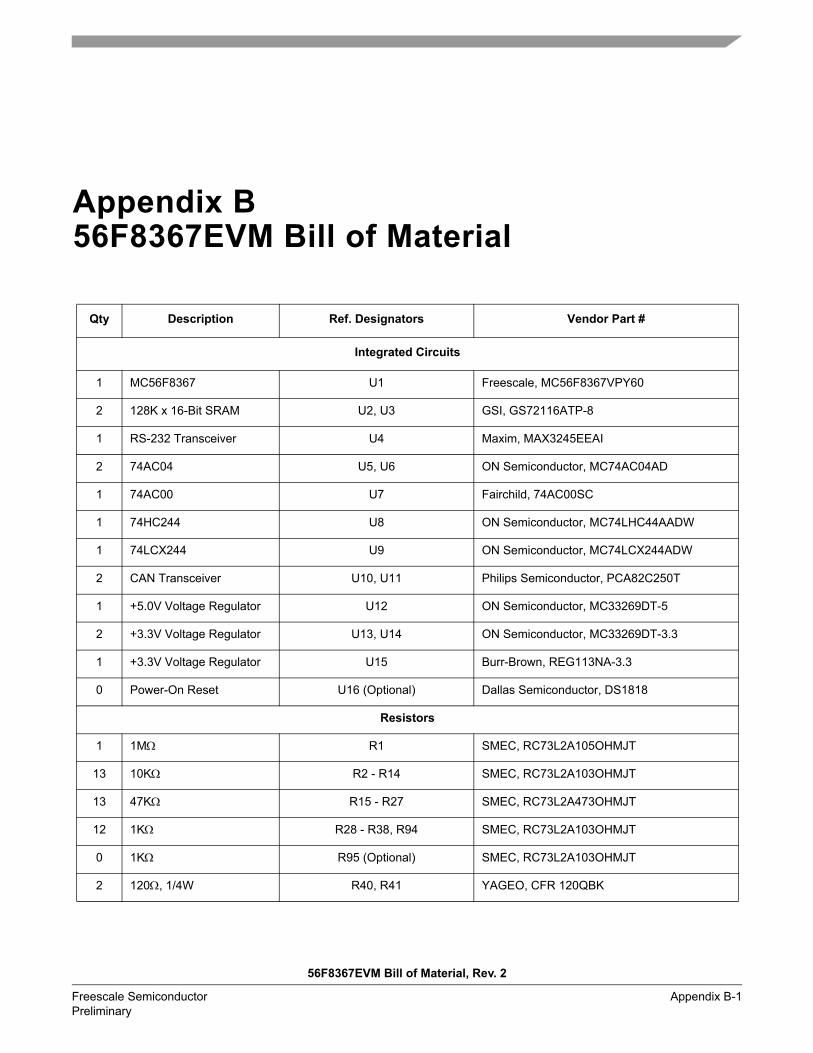
56F8367EVM Bill of Material, Rev. 2
Freescale Semiconductor Appendix B-1 Preliminary
Appendix B 56F8367EVM Bill of Material
Qty Description Ref. Designators Vendor Part #
Integrated Circuits
1 MC56F8367 U1 Freescale, MC56F8367VPY60
2 128K x 16-Bit SRAM U2, U3 GSI, GS72116ATP-8
1 RS-232 Transceiver U4 Maxim, MAX3245EEAI
2 74AC04 U5, U6 ON Semiconductor, MC74AC04AD
1 74AC00 U7 Fairchild, 74AC00SC
1 74HC244 U8 ON Semiconductor, MC74LHC44AADW
1 74LCX244 U9 ON Semiconductor, MC74LCX244ADW
2 CAN Transceiver U10, U11 Philips Semiconductor, PCA82C250T
1 +5.0V Voltage Regulator U12 ON Semiconductor, MC33269DT-5
2 +3.3V Voltage Regulator U13, U14 ON Semiconductor, MC33269DT-3.3
1 +3.3V Voltage Regulator U15 Burr-Brown, REG113NA-3.3
0 Power-On Reset U16 (Optional) Dallas Semiconductor, DS1818
Resistors
1 1MΩ R1 SMEC, RC73L2A105OHMJT
13 10KΩ R2 - R14 SMEC, RC73L2A103OHMJT
13 47KΩ R15 - R27 SMEC, RC73L2A473OHMJT
12 1KΩ R28 - R38, R94 SMEC, RC73L2A103OHMJT
0 1KΩ R95 (Optional) SMEC, RC73L2A103OHMJT
2 120Ω, 1/4W R40, R41 YAGEO, CFR 120QBK

MC56F8367EVM User Manual, Rev. 2
Appendix B-2 Freescale Semiconductor Preliminary
Resistors (Continued)
7 5.1KΩ R42 - R48 SMEC, RC73L2A512OHMJT
2 51Ω R50, R51 SMEC, RC73L2A51OHMJT
13 270Ω R52 - R64 SMEC, RC73L2A271OHMJT
1 10Ω R65 SMEC, RC73L2A100OHMJT
7 0Ω R66, R72 - R77 SMEC, RC73JP2A
0 0Ω R67 - R71 (Optional) SMEC, RC73JP2A
16 100Ω R78 - R93 SMEC, RC73L2A101OHMJT
Inductors
5 1.0mH FERRITE BEAD L1 - L5 Panasonic, EXC-ELSA35V
2 CAN Bus Filter L6, L7 EPCOS, B82790-S0513-N201
LEDs
2 Red LED LED1, LED4 Hewlett-Packard, HSMS-C650
5 Yellow LED LED2, LED5, LED7, LED9, LED11
Hewlett-Packard, HSMY-C650
6 Green LED LED3, LED6, LED8, LED10, LED12, LED13
Hewlett-Packard, HSMG-C650
Diode
1 +50V 1A BRIDGE RECT D1 DIODES, DF02S
1 S2B-FM401 D2 Vishay, DL4001DICT
0 S2B-FM401 D3, D4 (Optional) Vishay, DL4001DICT
Capacitors
1 470µF, +16V DC C1 ELMA, RV-16V471MH10R
4 47µF, +16V DC C2 - C5 ELMA, RV2-16V470M-R
4 2.2µF, +25V DC(Low ESR)
C6 - C9 TAIYO YUDEN, CELMK212BJ225MG-T
4 1.0µF, +25V DC C10 - C13 SMEC, MCCE105K3NR-T1
37 0.1µF C14 - C32, C35 - C51, C77 SMEC, MCCE104K2NR-T1
6 0.01µF C52 - C56, C76 SMEC, MCCE103K2NR-T1
Qty Description Ref. Designators Vendor Part #

56F8367EVM Bill of Material, Rev. 2
Freescale Semiconductor Appendix B-3Preliminary
Capacitors (Continued)
1 0.001µF C57 SMEC, MCCE102K2NR-T1
1 100pF C58 SMEC, MCCE101K2NR-T1
16 0.0022µF C59 - C74 SMEC, MCCE222K2NR-T1
1 10µF, +10V DC C75 KEMET, T494B106M010AS
Jumpers
4 3 × 1 Bergstick JG1, JG15, JG16, JG19 SAMTEC, TSW-103-07-S-S
12 1 × 2 Bergstick JG2 - JG7, JG10 - JG13, JG17, JG18
SAMTEC, TSW-102-07-S-S
3 2 × 2 Bergstick JG8, JG9, JG14 SAMTEC, TSW-102-07-S-D
Test Points
3 GND Test Point TP1, TP2, TP3 KEYSTONE, 5001, BLACK
1 +3.3V Test Point TP4 KEYSTONE, 5000, RED
1 +3.3V A Test Point TP5 KEYSTONE, 5004, YELLOW
1 GNDA Test Point TP6 KEYSTONE, 5002, WHITE
1 +5.0V Test Point TP7 KEYSTONE, 5003, ORANGE
Crystals
1 8.00MHz Crystal Y1 CTS, ATS08ASM-T
Connectors
1 DB25M Connector P1 AMPHENOL, 617-C025P-AJ121
1 DE9S Connector P2 AMPHENOL, 617-C009S-AJ120
1 2.1mm coaxPower Connector
P3 Switchcraft, RAPC-722
1 Peripheral Daughter Card Connector
J1 HRS, FX6-100P-0.8SV2
1 Memory Bus Daughter Card Connector
J2 HRS, FX6-60P-0.8SV2
1 7 x 2 JTAG Header J3 SAMTEC, TSW-106-07-S-D
1 13 x 2 Header J4 SAMTEC, TSW-106-13-S-D
Qty Description Ref. Designators Vendor Part #

MC56F8367EVM User Manual, Rev. 2
Appendix B-4 Freescale Semiconductor Preliminary
Connectors (Continued)
1 9 x 2 Header J5 SAMTEC, TSW-106-09-S-D
1 8 x 2 Header J6 SAMTEC, TSW-106-08-S-D
2 7 x 2 Header J7, J8 SAMTEC, TSW-106-07-S-D
6 5 x 2 Header J9, J10, J20 - J23 SAMTEC, TSW-106-05-S-D
6 3 x 2 Header J11 - J15, J17 SAMTEC, TSW-106-03-S-D
3 2 x 2 Header J16, J18, J19 SAMTEC, TSW-106-02-S-D
Switches
3 SPST Push button S1 - S3 Panasonic, EVQ-PAD05R
Transistors
1 2N2222A Q1 ZETEX, FMMT2222ACT
Miscellaneous
18 Shunt SH1 - SH13 Samtec, SNT-100-BL-T
4 Rubber Feet RF1 - RF4 3M, SJ5018BLKC
Qty Description Ref. Designators Vendor Part #

INDEX
Index, Rev. 2
Freescale Semiconductor Index-1 Preliminary
Numerics1.2 Amp power supply 2-1756F8300 Peripheral User Manual 2-456F8357 Technical Data Sheet 2-48.00MHz crystal oscillator 2-1
AA/D Preface-ixADC Preface-ixAnalog-to-Digital
A/D Preface-ixAnalog-to-Digital Converter
ADC Preface-ix
CCAN Preface-ix
bus termination 2-1, 2-2bypass 2-1, 2-2interface 2-1
CAN in AutomationCiA Preface-ix
CAN physical layer peripheral 2-2CiA Preface-ixController Area Network
CAN Preface-ix
DD/A Preface-ixDaughter Card Expansion
interface 2-1Debugging 2-10Digital-to-Analog
D/A Preface-ixDSP56800E Reference Manual 2-4
EEnhanced On-Chip Emulation
EOnCE Preface-ixEOnce Preface-ixEvaluation Module
EVM Preface-ixEVM Preface-ixExternal oscillator frequency input 2-1
FFlexCAN Preface-ixFlexCAN Interface Module
FlexCAN Preface-ixFSRAM 2-1, 2-5, 2-6
GGeneral Purpose Input and Output
GPIO Preface-ixGPIO Preface-ix, 2-28
HHost Parallel Interface Connector 2-11Host Target Interface 2-11
IIC Preface-ixIntegrated Circuit
IC Preface-ix
JJoint Test Action Group
JTAG Preface-ixJTAG Preface-ix, 2-1JTAG/Enhanced OnCE (EOnCE) 1-1Jumper Group 1-4
JG1 1-4JG10 1-4JG11 1-4JG12 1-4JG13 1-4JG14 1-4JG15 1-4JG16 1-4JG17 1-4JG18 1-4JG19 1-4JG2 1-4JG3 1-4JG4 1-4JG5 1-4JG6 1-4JG7 1-4JG8 1-4JG9 1-4

MC56F8367EVM User Manual, Rev. 2
Index-2 Freescale Semiconductor Preliminary
LLED Preface-ixLight Emitting Diode
LED Preface-ixLow-profile Quad Flat Package
LQFP Preface-ixLQFP Preface-ix
MMPIO Preface-ix, 2-31Multi Purpose Input and Output
MPIO Preface-ix
OOn-board power regulation 2-3OnCE Preface-ixOn-Chip Emulation
OnCE Preface-ix
PParallel JTAG Host Target Interface 2-1PCB Preface-ixperipheral port signals 2-18Phase Locked Loop
PLL Preface-ixPLL Preface-ixPrinted Circuit Board
PCB Preface-ixPulse Width Modulation
PWM Preface-ixPWM Preface-ixPWMA-compatible peripheral 2-2PWMB-compatible peripheral 2-2
QQuadDec Preface-ixQuadrature Decoder
interface port 2-30QuadDec Preface-ix
RR/C Preface-xRAM Preface-xRandom Access Memory
RAM Preface-xRead-Only Memory
ROM Preface-xreal-time debugging 2-10Resistor/Capacitor Network
R/C Preface-xROM Preface-xRS-232 2-1
level converter 2-7schematic diagram 2-7
SSCI Preface-xSCI/MPIO-compatible peripheral 2-2Serial Communications Interface
SCI Preface-xSerial Peripheral Interface
SPI Preface-xSPI Preface-xSPI/MPIO-compatible peripheral 2-2SRAM Preface-x
external data 2-1external program 2-1
Static Random Access MemorySRAM Preface-x
TTimer-compatible peripheral 2-2
WWait State
WS Preface-xWS Preface-x


How to Reach Us:
Home Page:www.freescale.com
E-mail:[email protected]
USA/Europe or Locations Not Listed:Freescale SemiconductorTechnical Information Center, CH3701300 N. Alma School Road Chandler, Arizona 85224 +1-800-521-6274 or [email protected]
Europe, Middle East, and Africa:Freescale Halbleiter Deutschland GmbHTechnical Information CenterSchatzbogen 781829 Muenchen, Germany+44 1296 380 456 (English)+46 8 52200080 (English)+49 89 92103 559 (German)+33 1 69 35 48 48 (French)[email protected]
Japan:Freescale Semiconductor Japan Ltd. HeadquartersARCO Tower 15F1-8-1, Shimo-Meguro, Meguro-ku,Tokyo 153-0064, Japan0120 191014 or +81 3 5437 [email protected]
Asia/Pacific:Freescale Semiconductor Hong Kong Ltd.Technical Information Center 2 Dai King Street Tai Po Industrial Estate Tai Po, N.T., Hong Kong +800 2666 [email protected]
For Literature Requests Only:Freescale Semiconductor Literature Distribution CenterP.O. Box 5405Denver, Colorado 802171-800-441-2447 or 303-675-2140Fax: [email protected]
Freescale™ and the Freescale logo are trademarks of Freescale Semiconductor, Inc. All other product or service names are the property of their respective owners. This product incorporates SuperFlash® technology licensed from SST.© Freescale Semiconductor, Inc. 2005. All rights reserved.
MC56F8367EVMUMRev. 207/2005
Information in this document is provided solely to enable system and software implementers to use Freescale Semiconductor products. There are no express or implied copyright licenses granted hereunder to design or fabricate any integrated circuits or integrated circuits based on the information in this document.
Freescale Semiconductor reserves the right to make changes without further notice to any products herein. Freescale Semiconductor makes no warranty, representation or guarantee regarding the suitability of its products for any particular purpose, nor does Freescale Semiconductor assume any liability arising out of the application or use of any product or circuit, and specifically disclaims any and all liability, including without limitation consequential or incidental damages. “Typical” parameters that may be provided in Freescale Semiconductor data sheets and/or specifications can and do vary in different applications and actual performance may vary over time. All operating parameters, including “Typicals”, must be validated for each customer application by customer’s technical experts. Freescale Semiconductor does not convey any license under its patent rights nor the rights of others. Freescale Semiconductor products are not designed, intended, or authorized for use as components in systems intended for surgical implant into the body, or other applications intended to support or sustain life, or for any other application in which the failure of the Freescale Semiconductor product could create a situation where personal injury or death may occur. Should Buyer purchase or use Freescale Semiconductor products for any such unintended or unauthorized application, Buyer shall indemnify and hold Freescale Semiconductor and its officers, employees, subsidiaries, affiliates, and distributors harmless against all claims, costs, damages, and expenses, and reasonable attorney fees arising out of, directly or indirectly, any claim of personal injury or death associated with such unintended or unauthorized use, even if such claim alleges that Freescale Semiconductor was negligent regarding the design or manufacture of the part.


