MC33811, Solenoid Monitor Integrated Circuit · Solenoid Monitor Integrated Circuit (IC) The 33811...
18
Document Number: MC33811 Rev. 3, 8/2008 Freescale Semiconductor Advance Information * This document contains certain information on a new product. Specifications and information herein are subject to change without notice. © Freescale Semiconductor, Inc., 2007. All rights reserved. Solenoid Monitor Integrated Circuit (IC) The 33811 is a 5 channel Solenoid Monitor IC that is used to verify proper electrical and mechanical solenoid operation. The IC contains five solenoid driver voltage monitoring stages and a serial peripheral interface (SPI) for fault communication and setup. The IC has the ability to determine the correct movement of solenoid armatures by analyzing the variation in the voltage profile, across the solenoid driver MOSFET, which represents the actual solenoid current profile. These features, along with cost effective packaging, make the 33811 ideal for powertrain solenoid monitoring applications. Features • Typical operating voltage range, 10.5 < VPWR < 15.5 volts • Interfaces to 3.3 and 5 volt microprocessors via SPI protocol • Reset pin to initialize all 5 fault outputs • Internal voltage regulator • Internal oscillator • Unique solenoid current profile detection circuitry • Pb-free packaging designated by suffix code EG Figure 1. 33811 Simplified Application Diagram SOLENOID MONITOR EG SUFFIX (PB_FREE) 98ASB42567B 16-PIN SOICW 33811 ORDERING INFORMATION Device Temperature Range (T A ) Package MCZ33811EG/R2 -40°C to 125°C 16 SOICW VDD SI SO SCLK CS MOSI MISO SCLK CS V BAT SOLM5 MCU VSPI RESET 33811 V BAT V BAT D_GND SOLENOID DRIVER V BAT V BAT V BAT OUT1 OUT2 OUT3 OUT4 OUT5 VPWR VDD SOLENOIDS SOLM4 SOLM3 SOLM1 IN1 IN2 IN3 IN4 IN5 PORTS P00 P01 P02 P05 P04 P03 A_GND SOLM2
Transcript of MC33811, Solenoid Monitor Integrated Circuit · Solenoid Monitor Integrated Circuit (IC) The 33811...

Document Number: MC33811Rev. 3, 8/2008
Freescale Semiconductor Advance Information
Solenoid Monitor Integrated Circuit (IC)
The 33811 is a 5 channel Solenoid Monitor IC that is used to verify proper electrical and mechanical solenoid operation. The IC contains five solenoid driver voltage monitoring stages and a serial peripheral interface (SPI) for fault communication and setup. The IC has the ability to determine the correct movement of solenoid armatures by analyzing the variation in the voltage profile, across the solenoid driver MOSFET, which represents the actual solenoid current profile.
These features, along with cost effective packaging, make the 33811 ideal for powertrain solenoid monitoring applications.
Features• Typical operating voltage range, 10.5 < VPWR < 15.5 volts• Interfaces to 3.3 and 5 volt microprocessors via SPI protocol• Reset pin to initialize all 5 fault outputs• Internal voltage regulator• Internal oscillator• Unique solenoid current profile detection circuitry• Pb-free packaging designated by suffix code EG
Figure 1. 33811 Simplified Application Diagram
SOLENOID MONITOR
EG SUFFIX (PB_FREE)98ASB42567B16-PIN SOICW
33811
ORDERING INFORMATION
Device Temperature Range (TA) Package
MCZ33811EG/R2 -40°C to 125°C 16 SOICW
VDD
SI
SO
SCLKCS
MOSI
MISO
SCLKCS
VBAT
SOLM5
MCUVSPI
RESET
33811VBAT
VBAT
D_GND
SOLENOID DRIVER
VBAT
VBAT
VBAT
OUT1
OUT2
OUT3
OUT4
OUT5
VPWR
VDD
SOLENOIDS
SOLM4SOLM3
SOLM1
IN1
IN2
IN3
IN4
IN5
PORTS
P00
P01
P02
P05
P04
P03
A_GND
SOLM2
* This document contains certain information on a new product. Specifications and information herein are subject to change without notice.
© Freescale Semiconductor, Inc., 2007. All rights reserved.

INTERNAL BLOCK DIAGRAM
INTERNAL BLOCK DIAGRAM
Figure 2. 33811 Simplified Internal Block Diagram
VPWR, VDD, 5.0 VOscillator
SI
SCLKCS
SO
SPI Interface
Waveform Detection Circuitry
RESETSOLM1
VPWR
VDD
D_GND
15µA15µA
VDD
and Clock Generator
Waveform Detection Circuitry SOLM3
Waveform Detection Circuitry SOLM2
Waveform Detection Circuitry SOLM4
Waveform Detection Circuitry SOLM5
A_GND
VSPI
Analog Integrated Circuit Device Data 2 Freescale Semiconductor
33811
PIN CONNECTIONS
PIN CONNECTIONS
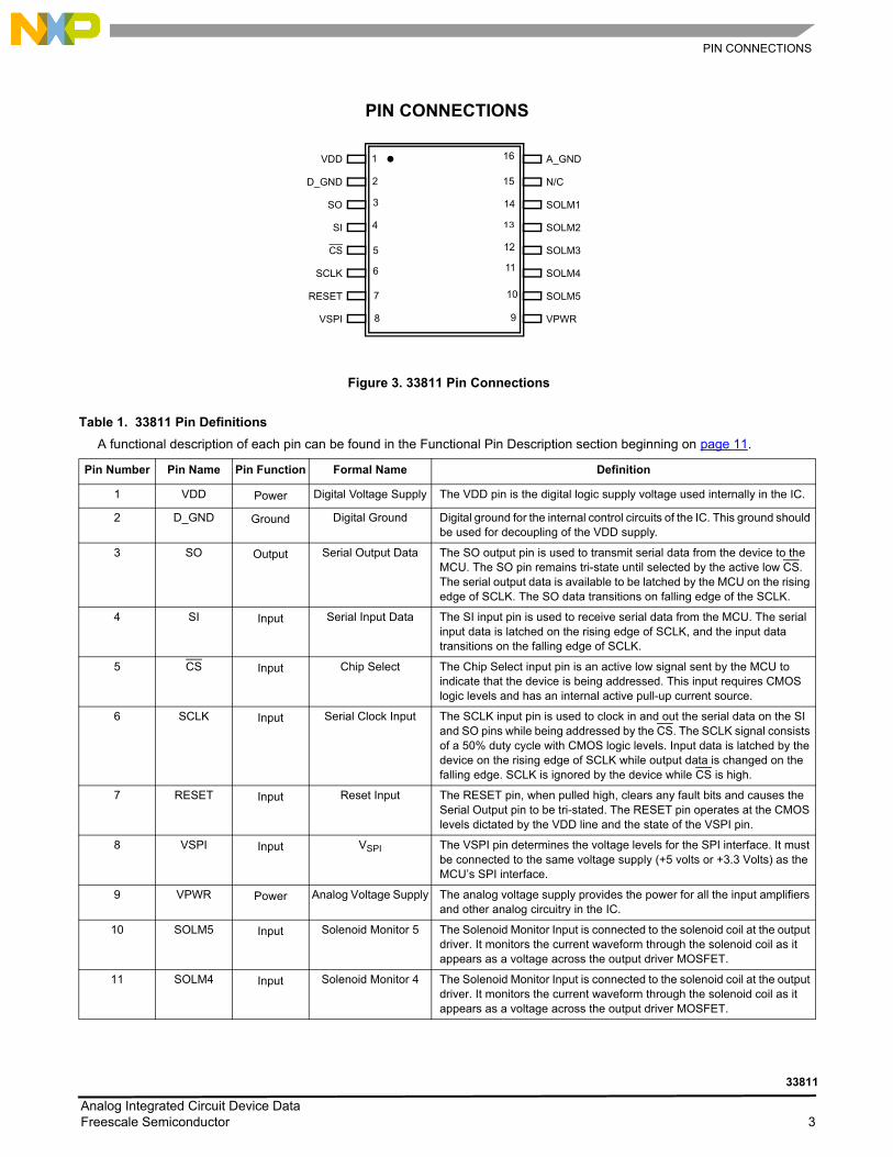
Figure 3. 33811 Pin Connections
1
2
3
4
5
6
16
15
7
8
14
13
12
11
10
9
A_GND
N/C
SOLM1
SOLM2
SOLM3
SOLM4
SOLM5
VPWR
VDD
D_GND
RESET
VSPI
SO
SI
SCLK
CS
Table 1. 33811 Pin Definitions A functional description of each pin can be found in the Functional Pin Description section beginning on page 11.
Pin Number Pin Name Pin Function Formal Name Definition
1 VDD Power Digital Voltage Supply The VDD pin is the digital logic supply voltage used internally in the IC.
2 D_GND Ground Digital Ground Digital ground for the internal control circuits of the IC. This ground should be used for decoupling of the VDD supply.
3 SO Output Serial Output Data The SO output pin is used to transmit serial data from the device to the MCU. The SO pin remains tri-state until selected by the active low CS. The serial output data is available to be latched by the MCU on the rising edge of SCLK. The SO data transitions on falling edge of the SCLK.
4 SI Input Serial Input Data The SI input pin is used to receive serial data from the MCU. The serial input data is latched on the rising edge of SCLK, and the input data transitions on the falling edge of SCLK.
5 CS Input Chip Select The Chip Select input pin is an active low signal sent by the MCU to indicate that the device is being addressed. This input requires CMOS logic levels and has an internal active pull-up current source.
6 SCLK Input Serial Clock Input The SCLK input pin is used to clock in and out the serial data on the SI and SO pins while being addressed by the CS. The SCLK signal consists of a 50% duty cycle with CMOS logic levels. Input data is latched by the device on the rising edge of SCLK while output data is changed on the falling edge. SCLK is ignored by the device while CS is high.
7 RESET Input Reset Input The RESET pin, when pulled high, clears any fault bits and causes the Serial Output pin to be tri-stated. The RESET pin operates at the CMOS levels dictated by the VDD line and the state of the VSPI pin.
8 VSPI Input VSPI The VSPI pin determines the voltage levels for the SPI interface. It must be connected to the same voltage supply (+5 volts or +3.3 Volts) as the MCU’s SPI interface.
9 VPWR Power Analog Voltage Supply The analog voltage supply provides the power for all the input amplifiers and other analog circuitry in the IC.
10 SOLM5 Input Solenoid Monitor 5 The Solenoid Monitor Input is connected to the solenoid coil at the output driver. It monitors the current waveform through the solenoid coil as it appears as a voltage across the output driver MOSFET.
11 SOLM4 Input Solenoid Monitor 4 The Solenoid Monitor Input is connected to the solenoid coil at the output driver. It monitors the current waveform through the solenoid coil as it appears as a voltage across the output driver MOSFET.
Analog Integrated Circuit Device Data Freescale Semiconductor 3
33811

PIN CONNECTIONS
12 SOLM3 Input Solenoid Monitor 3 The Solenoid Monitor Input is connected to the solenoid coil at the output driver. It monitors the current waveform through the solenoid coil as it appears as a voltage across the output driver MOSFET.
13 SOLM2 Input Solenoid Monitor 2 The Solenoid Monitor Input is connected to the solenoid coil at the output driver. It monitors the current waveform through the solenoid coil as it appears as a voltage across the output driver MOSFET.
14 SOLM1 Input Solenoid Monitor 1 The Solenoid Monitor Input is connected to the solenoid coil at the output driver. It monitors the current waveform through the solenoid coil as it appears as a voltage across the output driver MOSFET.
15 N/C No Connect No Connect This pin is not to be used and must be left open in any design.
16 A_GND Ground Analog Ground The Analog Ground is the return for the VDD and VPWR supply.
Table 1. 33811 Pin Definitions (continued)A functional description of each pin can be found in the Functional Pin Description section beginning on page 11.
Pin Number Pin Name Pin Function Formal Name Definition
Analog Integrated Circuit Device Data 4 Freescale Semiconductor
33811

ELECTRICAL CHARACTERISTICSMAXIMUM RATINGS
ELECTRICAL CHARACTERISTICS
MAXIMUM RATINGS
Table 2. Maximum Ratings
All voltages are with respect to ground unless otherwise noted. Exceeding these ratings may cause a malfunction or permanent damage to the device.
Ratings Symbol Value Unit
ELECTRICAL RATINGS
Supply Voltage (continuous)VPWRVDDVSPI
VPWR
VDD
VSPI
-1.5 to 25-0.3 to 7.0-0.3 to 7.0
VDC
Supply Voltage (transient) on VPWR VPWRMAX -1.5 to 50 VDC
CS, SI, SO, SCLK, RESET – -0.3 to VSPI VDC
Solenoid Monitor Inputs Maximum Voltage (5ms. maximum duration) VINJMXMAX 64 VDC
Frequency of SPI Operation (VDD = 5.0V)(1) – 3.2 MHz
ESD Voltage(2)
Human Body Model(3)Machine Model
VESD1VESD2
±2000±200
V
THERMAL RATINGS
Peak Package Reflow Temperature During Reflow(4), (5) TPPRT Note 5 °C
Storage Temperature TSTG -55 to 150 °C
Operating Ambient Temperature TA -40 to 125 °C
Operating Junction Temperature TJ -40 to 150 °C
Notes1. This parameter is guaranteed by design but is not production tested.2. ESD testing is performed in accordance with the Human Body Model (HBM) (Per AEC-Q100-002, CZAP = 100pF, RZAP = 1500Ω) and
the Machine Model (MM) (Per AEC-Q100-002, CZAP = 200pF, RZAP = 0Ω). ESD data available upon request.3. All pins when tested individually.4. Pin soldering temperature limit is for 10 seconds maximum duration. Not designed for immersion soldering. Exceeding these limits may
cause malfunction or permanent damage to the device.5. Freescale’s Package Reflow capability meets Pb-free requirements for JEDEC standard J-STD-020C. For Peak Package Reflow
Temperature and Moisture Sensitivity Levels (MSL), Go to www.freescale.com, search by part number [e.g. remove prefixes/suffixes and enter the core ID to view all orderable parts. (i.e. MC33xxxD enter 33xxx), and review parametrics.
Analog Integrated Circuit Device Data Freescale Semiconductor 5
33811

ELECTRICAL CHARACTERISTICSSTATIC ELECTRICAL CHARACTERISTICS
STATIC ELECTRICAL CHARACTERISTICS
Table 3. Static Electrical Characteristics Characteristics noted under conditions 7.0V ≤ VPWR ≤ 17V, - 40°C ≤ TA ≤ 125°C, GND = 0V, unless otherwise noted. Typical
values noted reflect the approximate parameter means at TA = 25°C under nominal conditions, unless otherwise noted.
Characteristic Symbol Min Typ Max Unit
POWER INPUT (VPWR, IPWR, IVDD, VDD, IDD)
Analog Supply Voltage RangeFully Operational VPWR (FO) 10.5 – 15.5 V
Digital Logic Supply Voltage RangeFully Operational VDD (FO) 4.75 5.0 5.25 V
SPI Voltage Supply Voltage RangeFully Operational VSPI(FO) 3.0
3.35.0 5.25 V
Supply Current from VPWRAll Outputs Disabled (Normal & Default Mode) VPWR = 17V IPWR (ON) – 1.0 5.0 mA
Supply Current from VDDAll Outputs Disabled (Normal & Default Mode) VDD = 5.5V IDD (ON) 1.0 5.0 mA
Positive Threshold Voltage Point A (10.5V < = VPWR < = 15.5V) V+TH_A 0 0.5 1.0 mV
Positive Threshold Voltage Point A with Offset (10.5V < = VPWR < = 15.5V)
V+TH_A_OFFSET 1.5 mV
Positive Threshold Voltage Point B(10.5V < = VPWR < = 15.5V) V+TH_B 1.5 3.0 4.5 mV
Negative Threshold Voltage (10.5V < = VPWR < = 15.5V) V-TH 0 -0.5 -1.0 mV
Negative Threshold Voltage with Offset(10.5V < = VPWR < = 15.5V)
V-TH_OFFSET -1.5 mV
Logic Supply Voltage VDD 3.0 – 5.5 V
Logic Supply CurrentStatic Condition
IDD
250 400 700μA
SPI DIGITAL INTERFACE (VIH, VIL, VHYS, CIN, LOGICSS)
Input Logic High-voltage Thresholds (8) VIH 0.7 x VSPI – VSPI + 0.3 V
Input Logic Low-voltage Thresholds (8) VIL GND - 0.3 – 0.2 x VSPI V
Input Logic Voltage Hysteresis (8) VHYS 100 – 300 mV
Input Logic Capacitance (9) CIN – – 20 pF
Notes6. Output fault detection thresholds with outputs programmed OFF. Output fault detect thresholds are the same for output open and shorts.7. This parameter is guaranteed by design, however is not production tested.8. Parameter applies to SI, RESET, CS and is guaranteed by design.9. Undervoltage thresholds minimum and maximum include hysteresis.
Analog Integrated Circuit Device Data 6 Freescale Semiconductor
33811

ELECTRICAL CHARACTERISTICSSTATIC ELECTRICAL CHARACTERISTICS
Normal Mode Input Logic Pull-down Current 0.8V to 5.0V(SI)
ISPIPD
5.0 10 25μA
CS, RESET Pull-up Current (CS, RESET = 0)
IDEFAULTPU
-5.0 -10 -25μA
SCLK, Tri-state SO Output0.0 V to 5.0 V
I SCK, I TRISO
-10 – 10μA
CS Input Current CS = VSPI
ICS
-10 – 10μA
CS Leakage Current to VSPI
CS = 5.0V, VSPI = 0.0V
ICS(LKG)
– – 10μA
SO High-State Output Voltage ISOHIGH = -1.0mA
VSOHIGH
VSPI - 0.4 – –V
SO Low-State Output Voltage ISOLOW = 1.0 mA
VSOLOW
– – 0.4V
Solenoid Monitor Input Pull-up Current(VSOLM = 0V)
ISOLM_PU -2.5 -5 -12.5 μA
Solenoid Monitor Input Leakage Current(VSOLM = 64V)
ISOLM_LKG -10 – 10 μA
Table 3. Static Electrical Characteristics Characteristics noted under conditions 7.0V ≤ VPWR ≤ 17V, - 40°C ≤ TA ≤ 125°C, GND = 0V, unless otherwise noted. Typical
values noted reflect the approximate parameter means at TA = 25°C under nominal conditions, unless otherwise noted.
Characteristic Symbol Min Typ Max Unit
Analog Integrated Circuit Device Data Freescale Semiconductor 7
33811

ELECTRICAL CHARACTERISTICSDYNAMIC ELECTRICAL CHARACTERISTICS
DYNAMIC ELECTRICAL CHARACTERISTICS
Table 4. Dynamic Electrical Characteristics
Characteristics noted under conditions 10.5V ≤ VPWR ≤ 15.5V, - 40°C ≤ TA ≤ 125°C, GND = 0V, unless otherwise noted. Typical values noted reflect the approximate parameter means at TA = 25°C under nominal conditions, unless otherwise noted.
Characteristic Symbol Min Typ Max Unit
SPI DIGITAL INTERFACE TIMING(10)
Required High State Duration on RESET for Reset to occur(11)
t RESET 1.0 – – μs
Falling Edge of CS to Rising Edge of SCLK Required Setup Time t LEAD 100 – – ns
Falling Edge of SCLK to Rising Edge of CS Required Setup Time t LAG 0 50 ns
SI to Rising Edge of SCLK Required Setup Time t SI (SU) 16 – – ns
Rising Edge of SCLK to SI Required Hold Time t SI (HOLD) 20 – – ns
SI, CS, SCLK Signal Rise Time(12) t R (SI) – 5.0 – ns
SI, CS, SCLK Signal Fall Time(12) t F (SI) – 5.0 – ns
Time from Falling Edge of CS to SO Low-impedance(13) t SO (EN) – 65 80 ns
Time from Rising Edge of CS to SO High-impedance(14) t SO (DIS) – – 55 ns
Time from Falling Edge of SCLK to SO Data Valid(15) t VALID – 65 90 ns
Sequential Transfer RateTime required between data transfers
tSTR 1.0 µs
Input Capacitance (SI, SCLK) CINPUT 7 15 pF
Load Capacitance (SO) CLOAD 200 pF
Tri-state Output Capacitance (SO) CTRI-STATE 20 pF
WAVEFORM DETECTION TIMINGS
Start of Activation Filter Time(16) tBEGIN 200 400 600 µs
Detection Window Time tWINDOW 40 53 66 ms
Sample Time tSAM 72 µs
Notes: 10. These parameters are guaranteed by design. Production test equipment uses 3.2MHz, 5.0V SPI interface.11. This parameter is guaranteed by design, however it is not production tested.12. Rise and Fall time of incoming SI, CS, and SCLK signals suggested for design consideration to prevent the occurrence of double pulsing.13. Time required for valid output status data to be available on SO pin.14. Time required for output states data to be terminated at SO pin.15. Time required to obtain valid data out from SO following the fall of SCLK with 200pF load.16. 9 µs guard band included in maximum limit
Analog Integrated Circuit Device Data 8 Freescale Semiconductor
33811

ELECTRICAL CHARACTERISTICSTIMING DIAGRAMS
TIMING DIAGRAMS
Figure 4. SPI Timing Characteristics
ParallelPorts
Microcontroller 33811
33811
SI
SCLKCS
SI
SO
SCLK
CS
SOSCLKMISO
MOSI
Shift Register
tSO(DIS)
0.7 VDD
0.2 VDD
0.2 VDD
0.7 VDD0.2 VDD
tLEAD
tSO(EN)
tSI(SU) tSI(HOLD)
tVALID
tLAG
CS
SCLK
SI
SO
MSB IN
MSB OUT LSB OUT0.7 VDD0.2 VDD
Analog Integrated Circuit Device Data Freescale Semiconductor 9
33811

ELECTRICAL CHARACTERISTICSMICROCONTROLLER PARAMETRICS
MICROCONTROLLER PARAMETRICS
SPI - MCU INTERFACE DESCRIPTION
The 33811 device directly interfaces to a 3.3V or 5.0V micro controller unit (MCU) using 16 bit Serial Peripheral Interface (SPI) protocol. SPI serial clock frequencies up to 3.2MHz may be used when programming and reading output status information (production tested at 3.2MHz). Figure 5 illustrates the serial peripheral interface (SPI) configuration between an MCU and one 33811.
Command data is sent to the 33811 device through the SI input pin. As data is being clocked into the SI pin, status information is being clocked out of the device by the SO output pin. The response data received by the MCU during SPI communication depends on the previous SPI message sent to the device. Next SO response data is listed at the bottom of each command table.
SPI Integrity CheckChecking the integrity of the SPI communication with the
initial power-up of the VDD and RESET pins is recommended. After initial system start-up or reset, the MCU will write one 16-bit pattern to the 33811. The first 8 bits read by the MCU will be the fault status (SO message 1) of the outputs. The second 8 bits will be the same bit pattern sent by the MCU. By the MCU receiving the same bit pattern it sent, bus integrity is confirmed. The second 16-bit pattern the MCU sends to the device is the a command word and will be operated on by the device accordingly on rising edge of CS.
Important A SCLK pulse count strategy has been implemented to ensure integrity of SPI communications. SPI messages consisting of 16 SCLK pulses and multiples of 8 clock pulses thereafter will be acknowledged. SPI messages consisting of other than 16 + multiples of 8 SCLK pulses will be ignored by the device.
Figure 5. SPI Interface with Microprocessor Two or more 33811 devices may be used in a module
system. Multiple ICs may be SPI-configured in parallel or serial. Figures 6 shows the configurations. When using the serial configuration, 32-clock cycles are required to transfer data in / out of the ICs.
Figure 6. SPI Parallel Interface with Microprocessor
33811Microcontroller
ReceiveBuffer
ParallelPorts
Fault Bits
16-Bit Shift RegisterShift Register
MOSI SI
MISO SO
SCLK
CS
ParallelPorts
Microcontroller 33811
33811
SI
SCLKCS
SI
SO
SCLK
CS
SCLKMISO
MOSI
Shift Register
SO
Analog Integrated Circuit Device Data 10 Freescale Semiconductor
33811
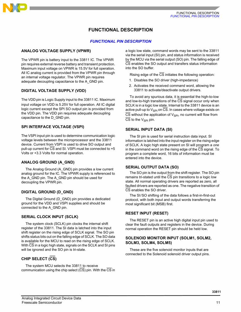
FUNCTIONAL DESCRIPTIONFUNCTIONAL PIN DESCRIPTION
FUNCTIONAL DESCRIPTION
FUNCTIONAL PIN DESCRIPTION
ANALOG VOLTAGE SUPPLY (VPWR)
The VPWR pin is battery input to the 33811 IC. The VPWR pin requires external reverse battery and transient protection. Maximum input voltage on VPWR is 15.5V for full operation. All IC analog current is provided from the VPWR pin through an internal voltage regulator. The VPWR pin requires adequate decoupling capacitance to the A_GND pin.
DIGITAL VOLTAGE SUPPLY (VDD)
The VDD pin is Logic Supply input to the 33811 IC. Maximum input voltage on VDD is 5.25V for full operation. All IC digital logic current except the SPI SO output pin is provided from the VDD pin. The VDD pin requires adequate decoupling capacitance to the D_GND pin.
SPI INTERFACE VOLTAGE (VSPI)
The VSPI input pin is used to determine communication logic voltage levels between the microprocessor and the 33811 device. Current from VSPI is used to drive SO output and pull-up current for CS and SI. VSPI must be connected to +5 Volts or +3.3 Volts for normal operation.
ANALOG GROUND (A_GND)
The Analog Ground (A_GND) pin provides a low current analog ground for the IC. The VPWR supply is referenced to the A_GND pin. The A_GND pin should be used for decoupling the VPWR pin.
DIGITAL GROUND (D_GND)
The Digital Ground (D_GND) pin provides a dedicated ground for the VDD and VSPI supplies and should be connected to the A_GND pin.
SERIAL CLOCK INPUT (SCLK)
The system clock (SCLK) pin clocks the internal shift register of the 33811. The SI data is latched into the input shift register on the rising edge of SCLK signal. The SO pin shifts status bits out on the falling edge of SCLK. The SO data is available for the MCU to read on the rising edge of SCLK. With CS in a logic high state, signals on the SCLK and SI pins will be ignored and the SO pin is tri-state.
CHIP SELECT (CS)
The system MCU selects the 33811 to receive communication using the chip select (CS) pin. With the CS in
a logic low state, command words may be sent to the 33811 via the serial input (SI) pin, and status information is received by the MCU via the serial output (SO) pin. The falling edge of CS enables the SO output and transfers status information into the SO buffer.
Rising edge of the CS initiates the following operation:1. Disables the SO driver (high-impedance)2. Activates the received command word, allowing the
33811 to activate/deactivate output drivers.
To avoid any spurious data, it is essential the high-to-low and low-to-high transitions of the CS signal occur only when SCLK is in a logic low state. Internal to the 33811 device is an active pull-up to VSPI on CS. In cases where voltage exists on CS without the application of VSPI, no current will flow from CS to the VSPI pin.
SERIAL INPUT DATA (SI)
The SI pin is used for serial instruction data input. SI information is latched into the input register on the rising edge of SCLK. A logic high state present on SI will program a one in the command word on the rising edge of the CS signal. To program a complete word, 16 bits of information must be entered into the device.
SERIAL OUTPUT DATA (SO)The SO pin is the output from the shift register. The SO pin
remains tri-stated until the CS pin transitions to a logic low state. All normal operating drivers are reported as zero, all faulted drivers are reported as one. The negative transition of CS enables the SO driver.
The SI / SO shifting of the data follows a first-in-first-out protocol, with both input and output words transferring the most significant bit (MSB) first.
RESET INPUT (RESET)
The RESET pin is an active high digital input pin used to clear the fault outputs and registers in the device. During normal operation the RESET pin should be held low.
SOLENOID MONITOR INPUT (SOLM1, SOLM2, SOLM3, SOLM4, SOLM5)
These are the five solenoid monitor inputs that are connected to the Solenoid solenoid driver output pins.
Analog Integrated Circuit Device Data Freescale Semiconductor 11
33811

FUNCTIONAL DESCRIPTIONFUNCTIONAL INTERNAL BLOCK DESCRIPTION
FUNCTIONAL INTERNAL BLOCK DESCRIPTION
Figure 7. Functional Internal Block Diagram
POWER SUPPLY AND OSCILLATORThe 33811 is designed to operate from 10.5V to 15.5V on
the VPWR pin. The VPWR pin supplies power to the internal regulator which, in turn, supplies the analog circuit blocks. The VDD Supply is used internally to supply the logic circuitry. The VSPI supply is used for setting the SPI communication threshold levels by supplying power to the SO driver and the SI and CS input buffers. The on-chip oscillator is used to set the solenoid sample period window and sample rate.
MCU INTERFACE:The 33811 device directly interfaces to a 3.3V or 5.0V
micro controller unit (MCU) using 16 bit Serial Peripheral Interface (SPI) protocol. SPI serial clock frequencies up to
3.2MHz may be used when programming and reading output status information. The RESET pin is used to place the 33811 into the Reset Mode. Normally the RESET pin is held at logic 0 by the MCU. When the MCU raises the RESET pin to a logic 1, the 33811 enters the reset Mode. The reset initializes the 5 fault outputs.
SOLENOID MONITORS: SOLM1 - SOLM5These are the five solenoid monitor inputs that are
connected to the external solenoid driver output pins. The IC has the ability to determine the correct movement of solenoid armatures by analyzing the variation in the voltage profile, across the solenoid driver MOSFET, which represents the actual solenoid current profile.
Analog Integrated Circuit Device Data 12 Freescale Semiconductor
33811
FUNCTIONAL DEVICE OPERATIONOPERATIONAL MODES
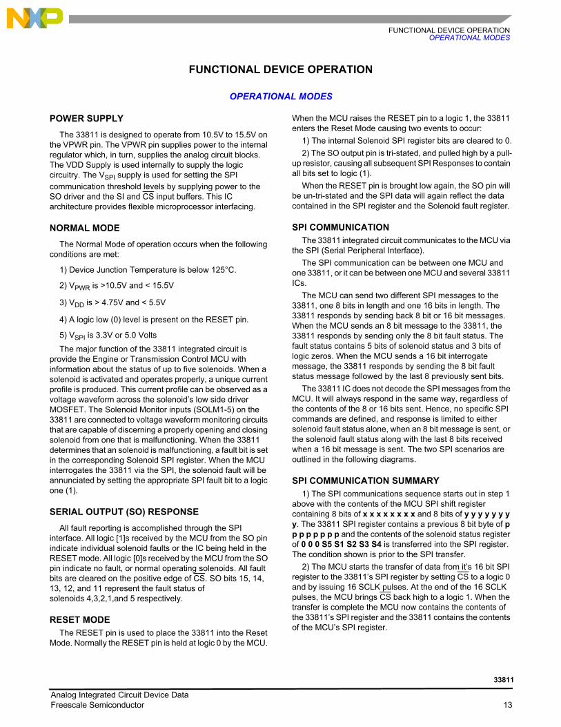
FUNCTIONAL DEVICE OPERATION
OPERATIONAL MODES
POWER SUPPLY
The 33811 is designed to operate from 10.5V to 15.5V on the VPWR pin. The VPWR pin supplies power to the internal regulator which, in turn, supplies the analog circuit blocks. The VDD Supply is used internally to supply the logic circuitry. The VSPI supply is used for setting the SPI communication threshold levels by supplying power to the SO driver and the SI and CS input buffers. This IC architecture provides flexible microprocessor interfacing.
NORMAL MODE
The Normal Mode of operation occurs when the following conditions are met:
1) Device Junction Temperature is below 125°C.
2) VPWR is >10.5V and < 15.5V
3) VDD is > 4.75V and < 5.5V
4) A logic low (0) level is present on the RESET pin.
5) VSPI is 3.3V or 5.0 Volts
The major function of the 33811 integrated circuit is provide the Engine or Transmission Control MCU with information about the status of up to five solenoids. When a solenoid is activated and operates properly, a unique current profile is produced. This current profile can be observed as a voltage waveform across the solenoid’s low side driver MOSFET. The Solenoid Monitor inputs (SOLM1-5) on the 33811 are connected to voltage waveform monitoring circuits that are capable of discerning a properly opening and closing solenoid from one that is malfunctioning. When the 33811 determines that an solenoid is malfunctioning, a fault bit is set in the corresponding Solenoid SPI register. When the MCU interrogates the 33811 via the SPI, the solenoid fault will be annunciated by setting the appropriate SPI fault bit to a logic one (1).
SERIAL OUTPUT (SO) RESPONSE
All fault reporting is accomplished through the SPI interface. All logic [1]s received by the MCU from the SO pin indicate individual solenoid faults or the IC being held in the RESET mode. All logic [0]s received by the MCU from the SO pin indicate no fault, or normal operating solenoids. All fault bits are cleared on the positive edge of CS. SO bits 15, 14, 13, 12, and 11 represent the fault status of solenoids 4,3,2,1,and 5 respectively.
RESET MODEThe RESET pin is used to place the 33811 into the Reset
Mode. Normally the RESET pin is held at logic 0 by the MCU.
When the MCU raises the RESET pin to a logic 1, the 33811 enters the Reset Mode causing two events to occur:
1) The internal Solenoid SPI register bits are cleared to 0.2) The SO output pin is tri-stated, and pulled high by a pull-
up resistor, causing all subsequent SPI Responses to contain all bits set to logic (1).
When the RESET pin is brought low again, the SO pin will be un-tri-stated and the SPI data will again reflect the data contained in the SPI register and the Solenoid fault register.
SPI COMMUNICATIONThe 33811 integrated circuit communicates to the MCU via
the SPI (Serial Peripheral Interface).The SPI communication can be between one MCU and
one 33811, or it can be between one MCU and several 33811 ICs.
The MCU can send two different SPI messages to the 33811, one 8 bits in length and one 16 bits in length. The 33811 responds by sending back 8 bit or 16 bit messages. When the MCU sends an 8 bit message to the 33811, the 33811 responds by sending only the 8 bit fault status. The fault status contains 5 bits of solenoid status and 3 bits of logic zeros. When the MCU sends a 16 bit interrogate message, the 33811 responds by sending the 8 bit fault status message followed by the last 8 previously sent bits.
The 33811 IC does not decode the SPI messages from the MCU. It will always respond in the same way, regardless of the contents of the 8 or 16 bits sent. Hence, no specific SPI commands are defined, and response is limited to either solenoid fault status alone, when an 8 bit message is sent, or the solenoid fault status along with the last 8 bits received when a 16 bit message is sent. The two SPI scenarios are outlined in the following diagrams.
SPI COMMUNICATION SUMMARY1) The SPI communications sequence starts out in step 1
above with the contents of the MCU SPI shift register containing 8 bits of x x x x x x x x and 8 bits of y y y y y y y y. The 33811 SPI register contains a previous 8 bit byte of p p p p p p p p and the contents of the solenoid status register of 0 0 0 S5 S1 S2 S3 S4 is transferred into the SPI register. The condition shown is prior to the SPI transfer.
2) The MCU starts the transfer of data from it’s 16 bit SPI register to the 33811’s SPI register by setting CS to a logic 0 and by issuing 16 SCLK pulses. At the end of the 16 SCLK pulses, the MCU brings CS back high to a logic 1. When the transfer is complete the MCU now contains the contents of the 33811’s SPI register and the 33811 contains the contents of the MCU’s SPI register.
Analog Integrated Circuit Device Data Freescale Semiconductor 13
33811

FUNCTIONAL DEVICE OPERATIONOPERATIONAL MODES
3) Step 3 demonstrates an 8 bit SPI transfer. The same exchange is performed, however, only 8 SCLK pulses are issued and only 8 bits of data are exchanged.
4) When the transfer is complete, only the eight bits of solenoid status has been transferred to the MCU. The data in the 33811’s SPI register lower 8 bits has been overwritten with the data from the MCU’s SPI register.
5) Step 5 shows the same scenario as step 3 however, before the transfer, the RESET pin is brought to a logic 1. This causes all data out of the SO pin to be a logical 1.
6) This step shows the contents of the MCU SPI register after the transfer. All bits are logical 1 because the RESET pin was held high for the duration of the transfer
WAVEFORM DETECTION ALGORITHM
Three Stage Current Waveform
An operational solenoid, once activated, produces a current waveform that consists of three distinct regions. The three regions are categorized by their relationship to a “dip” in the current that occurs when the solenoid armature moves within the coil. The regions are labeled the “Pre-Dip”, “Dip”, and “Post-Dip” regions. At this point, it should be noted that the 33811 does not monitor this current directly. It monitors the voltage across the low-side MOSFET driver. When the MOSFET is turned on, it can be thought of, to a first approximation, as a resistor with value RDS. Hence, any current variation through the solenoid, appears on the MOSFET drain, as a voltage variation, as is predicted by Ohm’s law. The 33811 is designed to monitor the voltage across the MOSFET and determine if the solenoid is operational or faulty based on the voltage waveform that is produced.
Activation of the SolenoidIf the solenoid is not activated, the low side MOSFET
driver is turned off, so almost the entire supply voltage appears across the MOSFET. When the MOSFET is activated, the voltage across it drops from the supply voltage to a voltage that depends on the instantaneous current flow through the solenoid and the RDS of the MOSFET. This dramatic voltage swing from the supply voltage, to near ground, triggers a timer in the 33811 IC. The time value of this timer is labeled TBEGIN and is 400 to 600μs in duration. If the voltage is still close to ground after TBEGIN, then the solenoid is deemed to be activated and the waveform detection algorithm is started.
The PRE-DIP Region
After dropping to near ground, the voltage across the MOSFET starts to increase as the current through the
solenoid begins to increase. The “Pre-Dip” region consists of a positive slope region, leading to a voltage maxima or peak, followed by a negative slope region. The 33811 monitors this voltage ramp up by sampling the voltage every 72μs and comparing it to the previous sample. If the new sample exceeds the previous sample by 0.5mV or more, the sampling comparator’s output is auto-zeroed to the new voltage level by adjusting the reference voltage to the input voltage and the sampling continues. At some point the voltage will reach a peak and the slope of the voltage curve will turn from positive to negative. The 33811 will continue sampling the voltage as it begins to descend but will not auto-zero the comparator until at least three consecutive samples of 3mV in magnitude have been detected.
The DIP Region
Once the three descending samples have been detected, sampling and auto-zeroing will continue to try to determine the next inflection point. This next inflection point will be the Dip which is caused by the successful travel of the solenoid’s armature. If a Dip is not discovered within the total time window of 56 mS. then the solenoid will be said to be faulty and the appropriate SPI register fault bit will be set to a logic 1. If the inflection point is discovered then sampling will continue.
The Post-DIP Region
After the Dip has occurred the waveform detection algorithm will continue sampling the voltage for the remainder of the 56mS. time window. If the voltage is still increasing after three sample times, then the solenoid is deemed to be operational and the appropriate SPI register fault bit is cleared to a logic 0. The waveform detection logic is then reset back to a state where it look for the next solenoid activation event.
Analog Integrated Circuit Device Data 14 Freescale Semiconductor
33811

FUNCTIONAL DEVICE OPERATIONOPERATIONAL MODES
Figure 8. Valid Solenoid Waveform
Analog Integrated Circuit Device Data Freescale Semiconductor 15
33811

PACKAGINGPACKAGE DIMENSIONS
PACKAGING
PACKAGE DIMENSIONS
For the most current package revision, visit www.freescale.com and perform a keyword search using the “98A” listed below.
EG SUFFIX16-PIN
PLASTIC PACKAGE98ASB42567B
ISSUE F
Analog Integrated Circuit Device Data 16 Freescale Semiconductor
33811

REVISION HISTORY
REVISION HISTORY
REVISION DATE DESCRIPTION OF CHANGES
1.0 4/2007 • Initial Release• Removed Peak Package Reflow Temperature During Reflow (solder reflow) parameter from
Maximum Ratings on page 5. • Added notes (4) and (5) to Maximum Ratings
2.0 7/2007 • Updates to form and style.
3 8/2008 • Changed Part Number on page 1 from PCZ to MCZ.• Upgraded from Product Preview to Advance Information status.
Analog Integrated Circuit Device Data Freescale Semiconductor 17
33811

MC33811Rev. 38/2008
Information in this document is provided solely to enable system and software implementers to use Freescale Semiconductor products. There are no express or implied copyright licenses granted hereunder to design or fabricate any integrated circuits or integrated circuits based on the information in this document.
Freescale Semiconductor reserves the right to make changes without further notice to any products herein. Freescale Semiconductor makes no warranty, representation or guarantee regarding the suitability of its products for any particular purpose, nor does Freescale Semiconductor assume any liability arising out of the application or use of any product or circuit, and specifically disclaims any and all liability, including without limitation consequential or incidental damages. “Typical” parameters that may be provided in Freescale Semiconductor data sheets and/or specifications can and do vary in different applications and actual performance may vary over time. All operating parameters, including “Typicals”, must be validated for each customer application by customer’s technical experts. Freescale Semiconductor does not convey any license under its patent rights nor the rights of others. Freescale Semiconductor products are not designed, intended, or authorized for use as components in systems intended for surgical implant into the body, or other applications intended to support or sustain life, or for any other application in which the failure of the Freescale Semiconductor product could create a situation where personal injury or death may occur. Should Buyer purchase or use Freescale Semiconductor products for any such unintended or unauthorized application, Buyer shall indemnify and hold Freescale Semiconductor and its officers, employees, subsidiaries, affiliates, and distributors harmless against all claims, costs, damages, and expenses, and reasonable attorney fees arising out of, directly or indirectly, any claim of personal injury or death associated with such unintended or unauthorized use, even if such claim alleges that Freescale Semiconductor was negligent regarding the design or manufacture of the part.
Freescale™ and the Freescale logo are trademarks of Freescale Semiconductor, Inc. All other product or service names are the property of their respective owners.© Freescale Semiconductor, Inc., 2007. All rights reserved.
How to Reach Us:
Home Page:www.freescale.com
Web Support:http://www.freescale.com/support
USA/Europe or Locations Not Listed:Freescale Semiconductor, Inc.Technical Information Center, EL5162100 East Elliot Road Tempe, Arizona 85284 +1-800-521-6274 or +1-480-768-2130www.freescale.com/support
Europe, Middle East, and Africa:Freescale Halbleiter Deutschland GmbHTechnical Information CenterSchatzbogen 781829 Muenchen, Germany+44 1296 380 456 (English)+46 8 52200080 (English)+49 89 92103 559 (German)+33 1 69 35 48 48 (French)www.freescale.com/support
Japan:Freescale Semiconductor Japan Ltd. Headquarters ARCO Tower 15F 1-8-1, Shimo-Meguro, Meguro-ku, Tokyo 153-0064Japan0120 191014 or +81 3 5437 [email protected]
Asia/Pacific:Freescale Semiconductor Hong Kong Ltd.Technical Information Center 2 Dai King Street Tai Po Industrial Estate Tai Po, N.T., Hong Kong +800 2666 [email protected]
For Literature Requests Only:Freescale Semiconductor Literature Distribution CenterP.O. Box 5405Denver, Colorado 802171-800-441-2447 or 303-675-2140Fax: [email protected]