MC33730, Switch Mode Power Supply with Multiple … Reference Voltage Bandgap Preference T-lim VBG...
28
Document Number: MC33730 Rev. 9.0, 8/2012 Freescale Semiconductor Advance Information * This document contains certain information on a new product. Specifications and information herein are subject to change without notice. © Freescale Semiconductor, Inc., 2009 - 2012. All rights reserved. Switch Mode Power Supply with Multiple Linear Regulators The 33730 is a multiple output power supply integrated circuit for automotive applications. The integrated circuit (IC) incorporates a switching regulator, which operates over a wide input voltage range from 4.5 to 26.5 V. The step-down switching regulator uses a fixed frequency pulse- width modulation (PWM) voltage mode control. It has a 3.5 A current limit (typical) and the slew-rate is adjustable via a control pin to reduce switching noise. The switching regulator has an adjustable frequency oscillator, which allows the user to optimize its operation over a wide range of input voltages and component values. The linear regulators can be configured either as two Normal mode regulators (V DD3 , V DDL ) and one standby regulator (V KAM ), or as one Normal mode linear regulator (V DDL ) and two standby regulators (V KAM and V DD3 Standby). Two protected outputs [VREF (1, 2)] are used to provide power to external sensors. Features • Provides all regulated voltages for Freescale 32-bit microcontroller family • Adjustable frequency switching buck regulator with slew-rate control • Power sequencing provided • Programmable voltages V DDL , V DD3 - 3% accuracy • Programmable standby regulator V KAM - 15% accuracy, operating down to 4.5 V at the KA_VBAT pin • V DD3 can be programmed as an optional second standby regulator with 15% accuracy • Provides two 5.0 V protected supplies for sensors • Provides reverse battery protection FET gate drive • Provides necessary MCU monitoring and fail-safe support Figure 1. 33730 Simplified Application Diagram SWITCHING POWER SUPPLY EK SUFFIX (PB-FREE) 98ARL10543D 32-LEAD SOICW-EP 33730 ORDERING INFORMATION Device (Add R2 Suffix for Tape and Reel) Temperature Range (T A ) Package MCZ33730EK - 40 °C to 125 °C 32-SOICW-EP MC33730EK * * Recommended device for all new designs VBAT KA_VBAT VIGN VREF1,2 GND HRT BOOT SW VDDH VCOMP VDD3_B VDD3 VDDL VKAM RSTs + + 5.0 V + + INV VDDL_B 5.0 V KA_1.0 V 1.5 V MCU (32 Bit) 3.3 V 33730 P1 P2 PFD P3 REGON IGN_ON CP 5.0V
Transcript of MC33730, Switch Mode Power Supply with Multiple … Reference Voltage Bandgap Preference T-lim VBG...

Document Number: MC33730Rev. 9.0, 8/2012
Freescale Semiconductor Advance Information
Switch Mode Power Supply with Multiple Linear Regulators
The 33730 is a multiple output power supply integrated circuit for automotive applications. The integrated circuit (IC) incorporates a switching regulator, which operates over a wide input voltage range from 4.5 to 26.5 V.
The step-down switching regulator uses a fixed frequency pulse-width modulation (PWM) voltage mode control. It has a 3.5 A current limit (typical) and the slew-rate is adjustable via a control pin to reduce switching noise. The switching regulator has an adjustable frequency oscillator, which allows the user to optimize its operation over a wide range of input voltages and component values.
The linear regulators can be configured either as two Normal mode regulators (VDD3, VDDL) and one standby regulator (VKAM), or as one Normal mode linear regulator (VDDL) and two standby regulators (VKAM and VDD3 Standby). Two protected outputs [VREF (1, 2)] are used to provide power to external sensors.
Features • Provides all regulated voltages for Freescale 32-bit
microcontroller family• Adjustable frequency switching buck regulator with slew-rate
control• Power sequencing provided• Programmable voltages VDDL, VDD3 - 3% accuracy• Programmable standby regulator VKAM - 15% accuracy,
operating down to 4.5 V at the KA_VBAT pin• VDD3 can be programmed as an optional second standby
regulator with 15% accuracy• Provides two 5.0 V protected supplies for sensors• Provides reverse battery protection FET gate drive• Provides necessary MCU monitoring and fail-safe support
Figure 1. 33730 Simplified Application Diagram
SWITCHING POWER SUPPLY
EK SUFFIX (PB-FREE)98ARL10543D
32-LEAD SOICW-EP
33730
ORDERING INFORMATION
Device (Add R2 Suffix for Tape and Reel)
Temperature Range (TA) Package
MCZ33730EK- 40 °C to 125 °C 32-SOICW-EP
MC33730EK *
* Recommended device for all new designs
VBAT
KA_VBATVIGN
VREF1,2
GND
HRT
BOOTSW
VDDH
VCOMPVDD3_B
VDD3
VDDL
VKAM
RSTs
+
+5.0 V
++
INV
VDDL_B
5.0 V
KA_1.0 V
1.5 V
MCU(32 Bit)
3.3 V
33730
P1P2
PFD
P3
REGON
IGN_ON
CP5.0V
* This document contains certain information on a new product. Specifications and information herein are subject to change without notice.
© Freescale Semiconductor, Inc., 2009 - 2012. All rights reserved.

DEVICE VARIATIONS
DEVICE VARIATIONS
Table 1. Device Variations Part no. Temperature Range Description
MCZ33730EK- 40 °C to 125 °C
Reset detect circuitry
MC33730EK Improved VDDL and VDD3 reset detect circuitry
Analog Integrated Circuit Device Data 2 Freescale Semiconductor
33730

INTERNAL BLOCK DIAGRAM
INTERNAL BLOCK DIAGRAM
Figure 2. 33730 Simplified Internal Block Diagram
5.0 VILIM=15 0mA
26.5 V,-1V,TLIM
UVLO/OVLO
VBAT
VBAT
KA_VBAT
VKAM
CP
PFD
REG ON
VIGN
IGN_ON
VREF1
VREF2
P1
P2
P3
RSTKAM
RSTH
RST3
RSTL
SW
SW
FREQ
BOOT
SR
INV
VCOMP
VDDH
VDD3_B
VDD3
VDDL_B
VDDL
HRT
GND
OscillatorFeed
ForwardRamp
Generator HS DriveLevelShifter
VKAM15 mA, ILIM,
TLIM
ProtectionFETDrive
ChargePump
Ref. VoltageProgramming
Block
5.0 VILIM=150 mA
26.5 V,-1V,TLIM
StandbyControl
Buck
Control Logic
CP
+–
+–
+–
Enable
VKAMReset Detect
VDDHReset Detect
VDD3Reset Detect
VDDLReset Detect
HR Timer
VKAM, VDDL, VDD3,VDD3_SBY
Reference Voltage
BandgapPreference
T-lim
VBG
VDD3ILim,
TLim
VDD3_SBYILim,
TLim
VDDLILim
10.4 K
1.98 KVBG
Analog Integrated Circuit Device Data Freescale Semiconductor 3
33730

PIN CONNECTIONS
PIN CONNECTIONS
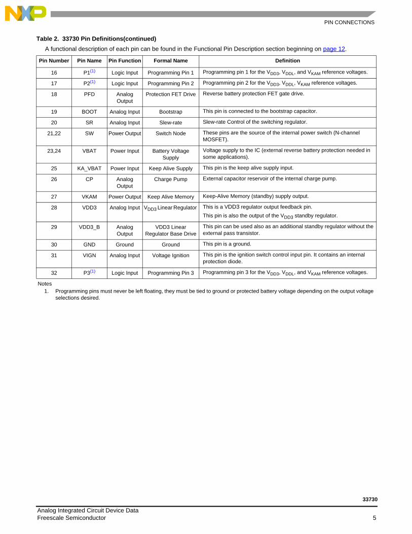
Figure 3. 33730 Pin Connections Table 2. 33730 Pin Definitions
A functional description of each pin can be found in the Functional Pin Description section beginning on page 12.
Pin Number Pin Name Pin Function Formal Name Definition
1 HRT Analog Output
Hardware Reset Timer This pin is the hardware reset timer programmed with an external resistor.
2 RSTKAM Open Drain VKAM Reset This pin is an open drain reset output, monitoring the VKAM supply to the microprocessor.
3 RSTH Open Drain VDDH Reset This pin is an open drain reset output, monitoring the VDDH regulator.
4 RSTL Open Drain VDDL Reset This pin is an open drain reset output, monitoring the VDDL regulator.
5 RST3 Open Drain VDD3 Reset This pin is an open drain reset output, monitoring the VDD3 regulator.
6 VREF2 Power Output VREF Output 2 This pin is the output of the protected supply VREF2. The pin is supplied from the VDDH through the protection FET.
7 VDDL Analog Input VDDL Regulator This pin is the VDDL regulator output feedback pin.
8 VDDH Analog/Power Input
VDDH Regulator This pin is the 5.0 V output feedback pin of the buck regulator. The pin is also a power input for the protected outputs VREF1,2.
9 VDDL_B Analog Output
VDDL Regulator Base Drive
VDDL linear regulator base drive.
10 VREF1 Power Output VREF Output 1 This pin is the output of the protected supply VREF1. The pin is supplied from the VDDH through the protection FET.
11 REGON Logic Input Regulator Hold On Regulator Hold On input pin (5.0 V logic level input).
12 IGN_ON Open Drain VIGN Status This open drain output signals the status of the VIGN pin.
13 VCOMP Analog Output
Compensation This pin provides switching pre-regulator compensation, it is the output of the error amplifier.
14 INV Analog Input Inverting Input Inverting input of the switching regulator error amplifier.
15 FREQ Analog Input Frequency Adjustment Frequency adjustment of the switching regulator. The value of the resistor to ground at this pin determines the oscillator frequency.
Note: The exposed pad is electrically and thermally connected to the IC ground.
HRTRSTKAM
RSTHRSTLRST3
VREF2VDDLVDDH
VDDL_BVREF1
REGONIGN_ONVCOMP
INVFREQ
P1
P3VIGNGNDVDD3_BVDD3VKAMCPKA_VBATVBATVBATSWSWSRBOOTPFDP2
12345678910111213141516
32313029282726252423222120191817
Analog Integrated Circuit Device Data 4 Freescale Semiconductor
33730
PIN CONNECTIONS
16 P1(1) Logic Input Programming Pin 1 Programming pin 1 for the VDD3, VDDL, and VKAM reference voltages.
17 P2(1) Logic Input Programming Pin 2 Programming pin 2 for the VDD3, VDDL, VKAM reference voltages.
18 PFD Analog Output
Protection FET Drive Reverse battery protection FET gate drive.
19 BOOT Analog Input Bootstrap This pin is connected to the bootstrap capacitor.
20 SR Analog Input Slew-rate Slew-rate Control of the switching regulator.
21,22 SW Power Output Switch Node These pins are the source of the internal power switch (N-channel MOSFET).
23,24 VBAT Power Input Battery Voltage Supply
Voltage supply to the IC (external reverse battery protection needed in some applications).
25 KA_VBAT Power Input Keep Alive Supply This pin is the keep alive supply input.
26 CP Analog Output
Charge Pump External capacitor reservoir of the internal charge pump.
27 VKAM Power Output Keep Alive Memory Keep-Alive Memory (standby) supply output.
28 VDD3 Analog Input VDD3 Linear Regulator This is a VDD3 regulator output feedback pin.This pin is also the output of the VDD3 standby regulator.
29 VDD3_B Analog Output
VDD3 Linear Regulator Base Drive
This pin can be used also as an additional standby regulator without the external pass transistor.
30 GND Ground Ground This pin is a ground.
31 VIGN Analog Input Voltage Ignition This pin is the ignition switch control input pin. It contains an internal protection diode.
32 P3(1) Logic Input Programming Pin 3 Programming pin 3 for the VDD3, VDDL, and VKAM reference voltages.
Notes1. Programming pins must never be left floating, they must be tied to ground or protected battery voltage depending on the output voltage
selections desired.
Table 2. 33730 Pin Definitions(continued)A functional description of each pin can be found in the Functional Pin Description section beginning on page 12.
Pin Number Pin Name Pin Function Formal Name Definition
Analog Integrated Circuit Device Data Freescale Semiconductor 5
33730

ELECTRICAL CHARACTERISTICSMAXIMUM RATINGS
ELECTRICAL CHARACTERISTICS
MAXIMUM RATINGS
Table 3. Maximum Ratings
All voltages are with respect to ground unless otherwise noted. Exceeding these ratings may cause a malfunction or permanent damage to the device.
Ratings Symbol Value Unit
Supply Voltage (VBAT) VBAT - 0.3 to +40 V
Keep-Alive Supply Voltage (KA_VBAT) KA_VBAT - 18 to +40 V
Control Inputs (VIGN, P1, P2, P3), PFD Output - 18 to +40 V
Bootstrap Voltage (BOOT, SR) referenced to ground VBOOT - 0.3 to +50 V
Bootstrap Voltage (BOOT, SR) referenced to SW VBOOT - VSW - 0.3 to +12 V
Charge Pump Output Voltage (CP) VCP - 0.3 to +12 V
Switch Node Voltage SW VSW - 2.0 to +40 V
Sensor Supplies (VREF1, VREF2) VREF - 1.0 to +26.5 V
Sensor Supplies (VREF1, VREF2) Maximum Slew Rate VREFMAXSR 2.0 V/µs
Regulator Voltages (VDDH,VDD3, VDD3_B, VDDL,VDDL_B, VKAM) VREG - 0.3 to +7.0 V
Open Drain Outputs (RSTH, RSTL, RST3, RSTKAM, IGN_ON) VDD - 0.3 to +7.0 V
Regon Input VREGON -0.3 to +7.0 V
Analog Inputs (VCOMP, INV, FREQ, HRT) VIN - 0.3 to + 3.0 V
ESD Voltage(2)
Human Body Model - HBM (all pins except BOOT, VDDL, RSTL)Human Body Model - HBM (Pins BOOT, VDDL, RSTL)Machine Model - MM (all pins)Charge Device Model - CDM (all pins)
VESD
± 2000± 1500± 200±750
V
Operational Package Temperature (Ambient Temperature) TA_MAX - 40 to + 125 °C
Storage Temperature TSTO - 65 to + 150 °C
Peak Package Reflow Temperature During Reflow(3), (4) TPPRT Note 4 °C
Maximum Junction Temperature TJ_MAX 150 °C
Thermal Resistance, Junction to Ambient(5) RθJ-A 41 °C/W
Thermal Resistance, Junction to Case(6) RθJ-C 1.2 °C/W
Notes2. ESD testing is performed in accordance with the Human Body Model (HBM) (AEC-Q100-2), the Machine Model (MM) (AEC-Q100-003),
RZAP = 0 Ω), and the Charge Device Model (CDM), Robotic (AEC-Q100-011).3. Pin soldering temperature limit is for 10 seconds maximum duration. Not designed for immersion soldering. Exceeding these limits may
cause malfunction or permanent damage to the device.4. Freescale’s Package Reflow capability meets Pb-free requirements for JEDEC standard J-STD-020C. For Peak Package Reflow
Temperature and Moisture Sensitivity Levels (MSL), Go to www.freescale.com, search by part number [e.g. remove prefixes/suffixes and enter the core ID to view all orderable parts. (i.e. MC33xxxD enter 33xxx), and review parametrics.
5. Thermal resistance measured in accordance with EIA/JESD51-2.6. Theoretical thermal resistance from the die junction to the exposed pad.
Analog Integrated Circuit Device Data 6 Freescale Semiconductor
33730

ELECTRICAL CHARACTERISTICSRECOMMENDED OPERATING CONDITIONS
RECOMMENDED OPERATING CONDITIONS
Table 4. Recommended Operating ConditionsAll voltages are with respect to ground unless otherwise noted.
Parameter Value Unit
Supply Voltages (VBAT, KA_VBAT) *6.0 to 26.5 V
Switching Regulator Output Current (IVDDH) total, VBAT = 6.0 to 26.5 V 0 to 2.0 A
VDD3 Standby Output Current 0 to 15 mA
VKAM Standby Output Current 0 to 15 mA
VREF1,2 Output Current 0 to 100 mA
Switching Frequency Range 100 to 500 kHz
* Tracks battery voltage from 6.0 down to 4.5 V.
Analog Integrated Circuit Device Data Freescale Semiconductor 7
33730

ELECTRICAL CHARACTERISTICSSTATIC ELECTRICAL CHARACTERISTICS
STATIC ELECTRICAL CHARACTERISTICS
Table 5. Static Electrical Characteristic Characteristics noted under conditions 6.0 V ≤ KA_VBAT = VBAT ≤ 26.5 V, - 40°C ≤ TA ≤ 125°C using the typical application circuit, unless otherwise noted.
Characteristic Symbol Min Typ Max Unit
GENERAL
Keep-Alive Start-up Voltage (at the KA_VBAT pin), VKAM Output Up VKAM_STUP 4.5 — — V
Start-up Voltage (at the KA_VBAT pin), VDD3, VDD3 standby, VDDL Up VSTUP 4.5 — — V
Over-voltage ShutdownVoltage at KA_VBAT pin rising VSHDN_R 35 — 42
V
Under-voltage Lock-outVoltage at KA_VBAT pin fallingVoltage at KA_VBAT pin rising
Under-voltage Lock-out Hysteresis(7)
VUVLO_FVUVLO_R
VUVLO_HYS
3.63.7—
——0.1
4.34.4—
V
Sleep Quiescent Current (Sleep mode)VIGN = 0 V, REGON = 0 V, IVKAM = 0 mA, VDD3 OFF, VBAT = 14.0 V,
KA_VBAT = 14 V (P1=1, P2=1, P3=1)
IQ— — 500
µA
SWITCHING REGULATOR (VDDH)
Buck Converter Output Voltage VBAT = 6.0 to 26.5 V, ILOAD = 100 mA
VBAT = 26.5 to 35 V, ILOAD = 100 mA
VDDH
4.94.85
5.05.0
5.15.15
V
Switching Regulator Current Limit (see Figure 5)Pulse-by-Pulse Current Limit
Extreme Current Limit (see Figure 5)(7)
ILIM_SWILIM_SW_EX
-2.25-3.75
-3.5-4.5
-4.25-6.00
A
SW Drain Source On Resistance(7)
ID = 500 mA, VBAT = 5.0 VRDS(ON)
— — 200mΩ
Thermal Shutdown Junction Temperature(7) TSH
TSL
—155
——
195—
°C
Thermal Shutdown Hysteresis(7) TSHYS 1.0 — 20 °C
VDD3 LINEAR REGULATOR
VDD3 Output Voltage (Includes Line and Load Regulation)IVDD3 = 0 to -500 mA, See Table 2 for VDD3 Output Settings
VDD3
-3.0 — 3.0%
VDD3 Dropout Voltage (VDDH - VDD3) IVDD3 = -800 mA (VDD3 set to 3.3 V via P1, P2, P3 and with an external transistor)
VDD3_DO
— 1.1 1.5V
VDD3_B Current Limit, VDD3_B = 0 V,KA_VBAT = 14 V, VBAT = 14 V
KA_VBAT = 5.0 V, VBAT = 5.0 V
IVDD3B_Lim
-20-20
——
-50-50
mA
Notes7. Guaranteed By Design.
Analog Integrated Circuit Device Data 8 Freescale Semiconductor
33730

ELECTRICAL CHARACTERISTICSSTATIC ELECTRICAL CHARACTERISTICS
VDD3 STANDBY LINEAR REGULATOR
VDD3 Standby Output Voltage (Includes Line and Load Regulation)IVDD3_SBY = 0 to -15 mA, See Table 2 for VDD3_SBY Output Setting
VDD3_SBY
-15 — 15%
VDD3 Dropout Voltage (KA_VBAT - VDD3) Standby Mode(VDD3 set at 3.3 V via P1, P2, P3) IVDD3 = -10 mA
VDD3_DO
— — 1.4V
VDD3 Standby Current Limit, VDD3 = 0 VKA_VBAT = 14 V, VBAT = 14 V
KA_VBAT = 5.0 V, VBAT = 5.0 V
IVDD3SBY_LIM
-20-20
——
-50-50
mA
Thermal Shutdown Junction Temperature(8) TSH
TSL
—150
——
190—
°C
Thermal Shutdown Hysteresis(8) TSHYS 5.0 — 20 °C
VDDL LINEAR REGULATOR
VDDL Output Voltage (Includes Line and Load Regulation)IVDDL = 0 to -500 mA, See Table 1 for VDDL Output Setting
VDDL
-3.0 — 3.0%
VDDL_B Dropout Voltage (VDDH - VDDL)
(VDDL set at 3.3 V via P1, P2, P3) IVDDL = -800 mA
VDDL_DO — — 280 mV
VDDL_B Current Limit, VDDL = 0 VKA_VBAT = 14 V, VBAT = 14 V
KA_VBAT = 5.0 V, VBAT = 5.0 V
IVDDL_LIM
-18-18
——
-50-50
mA
VKAM STANDBY LINEAR REGULATOR
VKAM Output Voltage (Includes Line and Load Regulation)IVKAM = 0 to -15 mA, See Table 1 for VKAM Output Setting
VKAM
-15 — 15%
VKAM Dropout Voltage (KA_VBAT - VKAM)IVKAM = -10 mA, VKAM set to 5.0 V (P1 = L, P2 = H, P3 = L)
VKAM_DO
— — 1.4V
VKAM STANDBY LINEAR REGULATOR (CONTINUED)
VKAM Current Limit, VKAM = 0 VKA_VBAT = 14 V, VBAT = 14 V
KA_VBAT = 5.0 V, VBAT = 5.0 V
IVKAM_LIM
-20-20
——
-50-50
mA
Thermal Shutdown Junction Temperature(8) TSH
TSL
—150
——
190—
°C
Thermal Shutdown Hysteresis(8) TSHYS 5.0 — 20 °C
Notes8. Guaranteed By Design.
Table 5. Static Electrical Characteristic(continued)Characteristics noted under conditions 6.0 V ≤ KA_VBAT = VBAT ≤ 26.5 V, - 40°C ≤ TA ≤ 125°C using the typical application circuit, unless otherwise noted.
Characteristic Symbol Min Typ Max Unit
Analog Integrated Circuit Device Data Freescale Semiconductor 9
33730

ELECTRICAL CHARACTERISTICSSTATIC ELECTRICAL CHARACTERISTICS
SENSOR SUPPLIES VREF1, VREF2
VREF On-resistance, IVREF = -100 mA RDS(ON) — — 500 mΩ
VREF Current Limit, VREF = -1.0 V(9) IREF_LIM -150 -280 -450 mA
VREF Reverse Current Limit, VREF = 26.5 V(9) IREF_REVLIM — — 40 mA
VREF Leakage Current, VREF Shut Down, VREF = -1.0 V(9) IREF_REVLIM -2.0 — — mA
Thermal Shutdown Junction Temperature(10) TSH
TSL
—150
——
190—
°C
Thermal Shutdown Hysteresis(10) TSHYS 5.0 — 20 °C
SUPERVISORY AND CONTROL CIRCUITS
VIGN Input Voltage ThresholdVBAT = 14.0 V, KA_VBAT = 14 V
VIGN_IHVIGN_IL
4.02.0
4.32.15
4.62.4
V
VIGN Hysteresis VIGN-HYS 1.7 — — V
VIGN Pull-down Current @ 5.0 VVBAT = 14.0 V, KA_VBAT = 14 V
IPD10 30 60
µA
REGON Input Voltage ThresholdVBAT = 14.0V, Battery Voltage = 14V
VIHVIL
1.7-0.3
——
—1.0
V
REGON Input Voltage Threshold Hysteresis VIHYS 0.1 0.3 0.4 V
REGON Pull-down Current @ 3.0 V IPD 5.0 — 30 µA
Programming Pin Input Voltage ThresholdVBAT = KA_VBAT = 14 V
VIHVIL
2.5-0.3
——
VBAT
1.0V
Programming P1, P2, P3 Leakage Current @ 14.0 V IPD — 1.0 5.0 µA
VDDH Reset Upper Threshold Voltage (ΔVDDH/VDDH) 4.0 8.0 13.0 %
VDDH Reset Lower Threshold Voltage (ΔVDDH/VDDH) -3.0 -8.0 -13.0 %
VDDL Reset Lower Threshold Voltage (ΔVDDL /VDDL) -3.0 -8.0 -13.0 %
VDD3 Reset Lower Threshold Voltage (ΔVDD3 /VDD3) -3.0 -8.0 -13.0 %
VDD3_SBY Reset Lower Threshold Voltage(ΔVDD3_SBY /VDD3_SBY) -3.0 -12.5 -30
%
VKAM Reset Lower Threshold Voltage (ΔVKAM /VkAM) -3.0 -12.5 -30 %
RSTH, RSTL, RST3, RSTKAM Low-level Output VoltageIOL = 5.0 mA — — 0.4
V
IGN_ON Low-level Output VoltageIOL = 5.0 mA — — 0.4
V
Notes9. The short circuit transient events on the VREF outputs must be limited to the voltage levels specified in the Maximum Ratings and slew
rates of less than 2.0 V/µs, otherwise damage to the part may occur. Refer to the paragraph Sensor Supplies (VREF1, VREF2) on page 18 and typical application circuit diagrams on Figure 8,and Figure 9 for recommended VREF output termination.
10. Guaranteed by design.
Table 5. Static Electrical Characteristic(continued)Characteristics noted under conditions 6.0 V ≤ KA_VBAT = VBAT ≤ 26.5 V, - 40°C ≤ TA ≤ 125°C using the typical application circuit, unless otherwise noted.
Characteristic Symbol Min Typ Max Unit
Analog Integrated Circuit Device Data 10 Freescale Semiconductor
33730

ELECTRICAL CHARACTERISTICSDYNAMIC ELECTRICAL CHARACTERISTICS
DYNAMIC ELECTRICAL CHARACTERISTICS
Table 6. Dynamic Electrical CharacteristicsCharacteristics noted under conditions 6.0 V ≤ KA_VBAT = VBAT ≤ 26.5 V, - 40°C ≤ TA ≤ 125°C using the typical application
circuit, unless otherwise noted.
Characteristic Symbol Min Typ Max Unit
GENERAL
Power On Reset Delay Time (HR Timer) (see Table 8)(Time to RESET up after Regulator in regulation)
tD_POR0 — 68
ms
Power On Reset Delay Time (HR Timer) Accuracy (33 k resistor) 8.0 — 12 ms
Programming Pin Latching Delay(11) tLD_P — 500 — µs
SWITCHING REGULATOR
Oscillator Frequency (Switching Freq.) Range - Adjustable (Figure 4) Freq 100 — 500 kHz
Oscillator Frequency Tolerance at 100 kHz (FREQ Pin Open) fTOL 90 — 110 kHz
SW Node Rise Time, VBAT = KA_VBAT = 14 V, ISW = 500 mA(11)
SR pin shorted to SW pinSR pin openSR pin shorted to BOOT pin
tSW_R———
0.961.822.38
———
V/ns
SW Node Fall Time, VBAT = KA_VBAT = 14 V, ISW = 500 mA(11)
SR pin shorted to SW pinSR pin openSR pin shorted to BOOT pin
tSW_F———
0.830.830.83
———
V/ns
Notes11. Guaranteed by design.
Analog Integrated Circuit Device Data Freescale Semiconductor 11
33730

FUNCTIONAL DESCRIPTIONINTRODUCTION
FUNCTIONAL DESCRIPTION
INTRODUCTION
The 33730 multi-output power supply integrated circuit addresses the system power supply needs for applications using the Freescale 32-bit microcontroller family architecture.
FUNCTIONAL PIN DESCRIPTION
HARDWARE RESET TIMER (HRT)This pin is the hardware reset timer input, which provides
delays for the Reset outputs. This delay is programmed by an external resistor to GND.
VKAM RESET (RSTKAM)This pin is an open drain reset output monitoring the VKAM
supply to the microprocessor. This output is actively pulled low when the VKAM output voltage falls below its reset threshold level.
VDDH RESET (RSTH)This pin is an open drain reset output monitoring the
VDDH regulator. This output is actively pulled low when the VDDH output voltage falls below its reset lower threshold level or when the VDDH output voltage exceeds its reset upper threshold level
VDDL RESET (RSTL)This pin is an open drain reset output monitoring the VDDL
regulator. This output is actively pulled low when the VDDL output voltage falls below its reset threshold level.
VDD3 RESET (RST3)This pin is an open drain reset output monitoring the VDD3
regulator. This output is actively pulled low when the VDD3 output voltage falls below its reset threshold level.
VREF OUTPUT 2 (VREF2)This pin is output of the protected supply VREF2. This
output supplies sensors outside of the electronic control module and therefore it is protected against a battery short and short to -1.0 V. This pin is supplied from the VDDH through the internal protection FET.
VDDL REGULATOR (VDDL)This pin is the VDDL regulator output feedback pin. The
emitter of VDDL regulator external NPN pass transistor is connected to this pin.
VDDH REGULATOR (VDDH)This pin is the 5.0 V output feedback pin of the buck
regulator. This pin is also a power input for the protected outputs VREF1 and VREF2.
VDDL REGULATOR BASE DRIVE (VDDL_B)VDDL linear regulator base drive. This output supplies
current into the base of the regulator external pass NPN transistor.
VREF OUTPUT 1 (VREF1)This pin is output of the protected supply VREF1. This
output supplies sensors outside of the electronic control module and therefore it is protected against short battery and short to -1.0 V. This pin is supplied from the VDDH through the internal protection FET.
REGULATOR HOLD ON (REGON)Regulator Hold On input control pin. The 33730 can be
enabled or kept in the Normal operational mode by holding this pin high. This is a 5.0 V logic input.
VIGN STATUS (IGN_ON)This open drain output signals the status of the VIGN pin.
This logic output is actively pulled low when the VIGN control input is pulled high.
COMPENSATION (VCOMP)This pin provides switching pre-regulator compensation
network. It is the output of the switching regulator error amplifier.
INVERTING INPUT (INV)This pin is the inverting input of the switching regulator
error amplifier.
FREQUENCY ADJUSTMENT (FREQ)This is the frequency adjustment input of the switching
regulator. The operating frequency of the switching regulator can be programmed by an external resistor from this pin to ground.
PROGRAMMING PIN 1 (P1)Programming Pin 1 for the VDD3, VDDL, and VKAM
reference voltage. The output voltage of the VDD3, VDDL and VKAM regulators can be programmed by the P1, P2, and P3 pins (see Table 7).
Analog Integrated Circuit Device Data 12 Freescale Semiconductor
33730

FUNCTIONAL DESCRIPTIONFUNCTIONAL PIN DESCRIPTION
PROGRAMMING PIN 2 (P2)Programming Pin 2 for the VDD3, VDDL, and VKAM
reference voltage. The output voltage of the VDD3, VDDL and VKAM regulators can be programmed by the P1, P2, and P3 pins (see Table 7).
PROGRAMMING PIN 3 (P3)Programming Pin 3 for the VDD3, VDDL, and VKAM
reference voltages. The output voltage of the VDD3, VDDL and VKAM regulators can be programmed by the P1, P2, and P3 pins (see Table 7).
PROTECTION FET DRIVE (PFD)Reverse battery protection FET gate drive. This pin is an
output drive for the gate of the external Reverse Battery Protection N-channel FET.
BOOTSTRAP (BOOT)This pin is connected to the bootstrap capacitor. It
provides the supply power for the switching regulator high-side drive.
SLEW-RATE (SR)Slew-rate Control of the switching regulator. The slew-rate
of the switching regulator can be adjusted by connecting this pin to switch node (SW pin, slow slew-rate selection), BOOT pin (fast slew-rate selection), or it can be left open (medium slew-rate selection).
SWITCH NODE (SW)This pin is the source of the switching regulator internal
power switch (N-channel MOSFET source).
BATTERY VOLTAGE SUPPLY (VBAT)Voltage supply to the IC (external reverse battery
protection is recommended).
KEEP ALIVE SUPPLY (KA_VBAT)This pin is the keep alive supply input. This input is reverse
battery protected. This input supplies power to the internal supply and bias circuits that have to do with this VKAM and other always-on supplies.
CHARGE PUMP (CP)External reservoir capacitor of the internal charge pump.
This charge pump provides the voltage needed to sufficiently enhance the gates of the internal n-channel mosfets (VREF1, VREF2, and VDDH) during the low battery condition.
KEEP ALIVE MEMORY (VKAM)Keep Alive Memory (standby) supply output. This output
supplies power for the module Keep-Alive memory. This output is always on, if the voltage at the KA_VBAT pin is above 4.5 V.
VDD3 LINEAR REGULATOR (VDD3)This is a VDD3 regulator output feedback pin.The emitter
of VDD3 regulator external NPN pass transitory is connected to this pin.
This pin can programmed to be the output of the VDD3 Standby regulator (see Table 7).
VDD3 LINEAR REGULATOR BASE DRIVE (VDD3_B)
This pin can be used also as an additional standby regulator without the external pass transistor.This output supplies current into the base of the regulator external pass NPN transistor.
GROUND (GND)This pin is the ground pin of the integrated circuit.
VOLTAGE IGNITION (VIGN)This pin is the turn-on control input that is controlled
through an ignition switch. This pin is reverse battery protected.
Analog Integrated Circuit Device Data Freescale Semiconductor 13
33730

FUNCTIONAL DESCRIPTIONFUNCTIONAL INTERNAL BLOCK DESCRIPTION
FUNCTIONAL INTERNAL BLOCK DESCRIPTION
5.0 VOLT BUCK REGULATORThis is the main regulator that supplies 5.0 Volts to the
following protected and regulated outputs, VREF1, VREF2, VDD3, and VDDL.
OSCILLATORThis is the frequency source for the switching (buck) 5 Volt
regulator. The frequency of oscillation is selected by an external resistor to ground.
BAND GAP REFERENCEThis is the main voltage reference, which is used as the
standard for all the current and voltage sources in the MC33730.
PROTECTION FET DRIVERThe protection FET is used to prevent reverse battery
connections from damaging the MC33730. The gate drive for the Protection FET is provided by this driver circuit.
SLEEP/WAKE CIRCUITRYThis circuitry is responsible for the two main modes of
operation for the MC33730, Sleep mode and Wake mode. In the Sleep mode, only the keep alive outputs are active, and the rest of the circuitry is in a low power drawing sleep state. In the Wake mode, the MC33730 is fully functional and normal current is being consumed.
IGNITION DRIVERThis block of circuitry controls all the voltage outputs,
except for the keep alive voltage output(s). It also provides an
output signal to indicate that the ignition switch has been activated.
VREF1This output is one of two protected 5.0 volt outputs that can
be used to supply external sensors or other analog circuits requiring a regulated, short-circuit protected 5.0 volt supply.
VREF2This output is one of two protected 5.0 volt outputs that can
be used to supply external sensors or other analog circuits requiring a regulated, short-circuit protected 5.0 volt supply.
VDD3 REGULATORThis is one of three, voltage programmable, regulated
supplies. This supply is controlled by the ignition switch.
VDDL REGULATORThis is one of three, voltage programmable, regulated
supplies. This supply is controlled by the ignition switch.
VKAMThis is one of three, voltage programmable, regulated
supplies. This supply is NOT controlled by the ignition switch.
VOLTAGE PROGRAMMINGP1, P2, and P3 are three logic level inputs that control the
voltage that is available on the VDD3, VDDL and VKAM outputs.
Table 7 indicates the 8 different combinations of P1, P2, and P3 and the resultant voltage values.
Band Gap Reference Sleep/Wake Circuitry
Voltage Programmming Input Protection FET Driver
Ignition Input
Oscillator
5 Volt Buck SwitchingRegulator
5 Volt Protected Outputs(VREF1, VREF2)
Linear Regulator Outputs(VDDL, VDD3, VKAM)
Ignition Driver
Reset Circuitry
Input Functions
Internal Functions
Output Functions
MC33730 - Functional Block Diagram
Analog Integrated Circuit Device Data 14 Freescale Semiconductor
33730

FUNCTIONAL DESCRIPTIONFUNCTIONAL INTERNAL BLOCK DESCRIPTION
RESET CIRCUITRYThere are four open drain reset lines that indicate the
status of the four voltage outputs; VDDH, VDDL, VDD3, and VKAM. They are labeled: RSTH, RSTL, RST3, and RSTKAM.
REGON INPUTThis input is OR’d with VIGN. However, it is a 5.0 volt logic
input, as opposed to VIGN, which is a VBAT level input. This input is controlled by an MCU I/O pin, to hold power up when the ignition switch is turned off, so housekeeping functions can be performed before power is shut off, by lowering the REGON line. IF REGON is not needed, it should be tied to GND.
Analog Integrated Circuit Device Data Freescale Semiconductor 15
33730

FUNCTIONAL DEVICE OPERATIONOPERATION DESCRIPTION
FUNCTIONAL DEVICE OPERATION
OPERATION DESCRIPTION
INTRODUCTIONThe 33730 has two supply inputs. The KA_VBAT pin is the
supply input for the standby regulators VKAM (and optionally VDD3_SBY, see Table 7) and for the internal supply circuits. The VBAT pin is the power input of the integrated buck regulator, which steps-down the protected battery voltage providing directly the 5.0 V system supply VDDH. VDDH provides power for the main linear regulator(s) VDDL, VDD3, and also for the other module circuits requiring 5.0 V supply voltage (e.g. protected VREF1,2 outputs).
If the supply voltage ramps from zero volts up to its nominal level, the 33730 will start at the latest when the supply (battery) voltage reaches VSTUP at the KA_VBAT pin. If the supply voltage ramps down, the 33730 will keep operating (with degradation of the output voltage regulation) down to VUVLO_f at the KA_VBAT pin. The VKAM output stays operational down to VUVLO_f at the KA_VBAT pin.
The 33730 will operate in systems with and without standby mode. In the Standby (sleep) mode of operation the IC will draw maximum IQ quiescent current, assuming only the VKAM is used as a standby output, and it is unloaded. When VDD3 is used as an additional standby output the quiescent current increases by approximately another 100 μA.
POWER UPThe 33730 will safely power up when the power is applied
simultaneously (hot plugged) or in the random sequence to the KA_VBAT, VBAT and VIGN (or REGON) inputs.
POWER DOWNThe 33730 will safely power down when the power is
disconnected from any of the KA_VBAT, VBAT inputs or when control signals the VIGN or REGON inputs go low.
UNDERVOLTAGE LOCK-OUT (UVLO)There is an under-voltage lock-out feature implemented
into the IC. When the battery voltage at the KA_VBAT pin falls below VUVLO_f the under-voltage comparator initiates the power down sequence for the whole IC. The under-voltage lock-out circuit has a VUVLO_hys hysteresis and 5.0 μs glitch filter in order to prevent spurious tripping its threshold level and consequent system oscillations between the ON and OFF states.
SWITCHING REGULATORThe 33730 switching regulator is a fixed frequency
(externally adjustable) PWM voltage mode controller with integrated low-RDS(ON) N-channel power MOSFET. This architecture is widely flexible and provides a possibility to
optimize its operation over a wide range of input voltages. The 33730 switching regulator provide the following features:
Adjustable Switching FrequencyThe adjustable frequency feature provides the ability to
modify the switcher performance for optimized cost (higher frequency, smaller, cheaper components), or higher efficiency and better EMC performance (lower switching frequency for reduced losses and EMI). The operating frequency of the switching regulator can be adjusted by means of an external resistor RF connected from the FREQ pin to ground (see Figure 4).
Figure 4. Switching Regulator Frequency vs. RFreq Value
Adjustable Slew-rateThe adjustable slew-rate option allows, with selection of
the right switching frequency, optimization of the system for EMC performance.
Over-voltage Lock-Out (Shutdown) The over-voltage lock-out (shutdown) feature turns the
switching regulator off when the input voltage exceeds the VSHDN_r limit. This extends the 33730 capability to survive the severe load dump conditions up to max VBAT.
Operation at 100% Duty CycleThe internal charge pump is used to enhance the power
MOSFET gate when the switching regulator reaches 100% duty cycle during the low battery conditions.
The switching regulator output voltage VDDH is regulated to provide 5.0 V @ 2.0 A with ±2% accuracy and it is intended
Frequency vs RFreq
0
100
200
300
400
500
600
0 20 40 60 80 100
RFreq [kohm]
Switc
hing
Fre
quen
cy [k
Hz]
FSW ≅ 18.48 + (5098.7/RFREQ)FSW is the switch frequency in kHzRFREQ is the resistor value in kOhms
Analog Integrated Circuit Device Data 16 Freescale Semiconductor
33730

FUNCTIONAL DEVICE OPERATIONOPERATION DESCRIPTION
to directly power the digital and analog circuits of the Electronic Control Module (ECM). The switching regulator output current is also used by the following linear regulators VDD3_3, VDDL, and sensor supplies VREF1, and VREF2.
The direct voltage conversion to VDDH = 5.0 V together with the Protection FET Driver circuit allows operation of the IC at very low battery voltages, which would otherwise require to use a boost regulator (with an additional system cost) or a different and more expensive switching converter topology (e.g. flyback).
Short Circuit ProtectionThe switching regulator is protected against the over-
current and short-circuit conditions. It integrates a current limit circuit, which has two threshold levels - the pulse by pulse, and the extreme.
Pulse by Pulse Current LimitPulse-by-Pulse Current Limit threshold has a nominal
value set ILIM_SW. When the current flowing through switching regulator power FET exceeds this value the power FET is immediately turned off. During the next switching cycle the power FET is turned on again until it is commanded off by its natural duty cycle or until the current reaches the threshold level again. It should be noted that the current limit is blanked for several tens of nanoseconds during the turn-on and turn-off transition times in order to prevent erroneous turn off due to the current spikes caused by switcher parasitic components.
Extreme Current Limit. In some cases, during the over-current or short-circuit
condition, the inductor current does not sufficiently decay during the off time of the switching period. The current rise during the current limit blanking time is higher than the decay during the off time. In this case the current in the inductor builds up every consecutive switching cycle. In order to prevent the power FET failure during this condition an extreme current limit has been implemented. When the current flowing through the power FET reaches the ILIM_SW_Ext threshold, the switching regulator will shut off for 500 μs, before the switching regulator is allowed to turn on again (see Figure 5).
Figure 5. 33730 Current Limit
Soft StartThe switching regulator has an integrated soft-start
feature. During the soft-start sequence the duty cycle of the internal power switch will be gradually increased from low value to the regulation level. This technique prevents any undesirable inrush current into the buck regulator output capacitor.
LINEAR REGULATORSThe 33730 integrates two linear regulator control circuits
VDD3 (programmable), VDDL (programmable) both capable of driving up to 15 mA (min.) base current into the external pass NPN transistors. The output voltage of both linear regulators is monitored at their feedback pins (VDD3 and VDDL). If the voltage at any of the VDD3, VDDL feedback pins fall below their regulation level, the supervisory Reset control circuits will assert the corresponding reset signal (RSTL, and/or RST3 lines will be pulled low). See Table 7 for the output voltage selection details.
The linear regulators will stay in regulation down to 4.5 V at the KA_VBAT pin.
The 33730 linear regulators offer high flexibility and variability of the module design in terms of selectable output voltages as well as wide range of output current capability. There several types of suitable external pass NPN transistors which could be used. The choice of the particular type depends mostly on the expected power dissipation of the pass transistor. The following parts provide good solution and have been bench tested with the 33730:
BCP68T1 (SOT-223)NJD2873T4 (DPAK)MJB44H11 (D2PAK)Available from ON Semiconductor.NOTE: The 33730 linear regulators have been designed to
use low ESR ceramic output capacitors - see Figure 8 and Figure 9 for the recommended values.
STANDBY REGULATORSThe 33730 integrates two standby linear regulators, the
VKAM and the optional standby regulator VDD3 (see Figure 9) for the optional standby circuit).The output voltage levels of both standby linear regulators are programmable and supervised by the Reset control circuits (RSTKAM, and/or RST3). Both the VKAM and VDD3 outputs are capable of delivering IVKAM_LIM and IVDD3_LIM of load current. See Table 7 for the VKAM and VDD3 standby output voltage selection details.
The VKAM standby regulator will keep functioning even below VUVLO_f but the specified drop out voltage may not be maintained.
NOTE: The 33730 standby regulators have been designed to use low ESR ceramic output capacitors - see Figure 8 and Figure 9 for recommended values.
tBLANK
TSW
ILim3.5A
4.5A
500us d elay TSW
0
InductorCu rrent
SwitcherFET Gate
Ext.ILim
Analog Integrated Circuit Device Data Freescale Semiconductor 17
33730

FUNCTIONAL DEVICE OPERATIONOPERATION DESCRIPTION
PROGRAMMING LINEAR REGULATOR OUTPUT VOLTAGE
The output voltage of the VDD3, VDDL and VKAM outputs can be externally programmed by placing logic levels on the programming pins P1, P2, and P3 (see Table 7). This extends the application flexibility of the IC without having to use an external resistor divider, thus improving the regulator accuracy over the whole temperature range, and reducing the component count.
The logic level of the programming pin (Px) can be selected by tying the pin to ground (logic level "0") or to protected battery voltage (logic level "1"). Programming pins must never be left floating, they must be tied to either ground or protected battery voltage.
The programming information is read and latched with the 500 μs delay after the power is applied to the IC.
LOW BATTERY OPERATIONWhen the battery voltage falls below the specified
minimum value, the 33730 switching regulator will enter a 100% duty cycle mode of operation and its output voltage VDDH will follow the decreasing battery voltage. If the battery voltage continues to fall, the VDDH voltage reaches its reset threshold level, and the RSTH signal will be pulled low, but the other linear regulators will continue to operate, and their monitoring signals stay high as long as the VDDH provides sufficient headroom for the regulators to stay in their regulation limits (see Figure 6 and Figure 7). If the battery voltage continues to fall, the linear regulators would not have sufficient headroom to stay in regulation, and their resets would be asserted (RSTL, RST3, or both would be pulled low). At that moment the power down sequence would be engaged.
The VKAM standby regulator will operate down to (VKAM and VKAM_DO) and VKAM-DO at the KA_VBAT pin.
POWER SEQUENCING (VDDH, VDD3, VDDL)VDDH, VDD3, and VDDL are power sequenced by means of
internal pull-down FETs. During the power up sequence, VDD3 and VDDL will follow VDDH.
During the power down sequence the VDD3 and VDDL outputs will be pulled down by the internal pull-down power FETs, and VDDH will be shut off with a defined delay (~100 μs typ.).
In order to engage the power down sequence, the following conditions have to be met:
(VIGN . REGON) + UVLO = Power DownThe VDD3 output is not power sequenced when used as a
standby regulator.
SENSOR SUPPLIES (VREF1, VREF2)There are two sensor supplies, VREF1 and VREF2,
integrated into the IC. They are internally connected to VDDH through power MOSFETs which protect against short to battery and short to ground conditions.
Severe fault conditions on the VREF1 and VREF2 outputs, like shorts to either ground or battery, will not disrupt the operation of the main regulator VDDH, or cause assertion of any Reset signal.
IMPORTANT NOTE:The VREF outputs MUST be externally protected against
transient voltage events with slew rates faster than 2.0 V/μs, otherwise damage to the part may occur. A practical and inexpensive solution consists of using a series RC network connected from the VREF output to ground (see Figures 8 and 9 for typical component values). Other means, such as a single electrolytic capacitor with its capacitance value C > 10 μF, may be also used.
PROTECTION FET DRIVE (PFD)The Protection FET Drive circuit allows using an optional
N-channel protection MOSFET (instead of a standard reverse protection diode) to protect against a reverse battery voltage condition. This approach improves the operating capabilities at very low battery voltages.
An internal charge pump is used to enhance the Protection FET gate during nominal and low battery conditions. The charge pump will be enabled at the startup voltage. When the battery voltage gets sufficiently high, the Protection FET is turned off and the integrated circuit power input (VBAT pins) are supplied through the body diode of the Protection FET.
Use of the Protection FET is not necessary in systems already using a protection diode, relay or when no reverse battery protection is required.
CONTROL INPUT (VIGN)The VIGN pin is used as a control input to the IC. The
regulation circuits will function and draw current from VBAT when VIGN is high (active) or when the REGON pin is high. The VIGN pin has a VIHN-IH power-up threshold VIGN-IL typical power-down threshold) and VIGN-HYS (minimum) of hysteresis. VIGN is designed to operate up to max VBAT battery while providing reverse battery and max VBAT load dump protection.
Table 7. Programming VDD3, VDDL, VKAM Output Voltage
P1 P2 P3 VDD3 VDDL VKAM
High High High 3.3 V 2.6 V 2.6 V
High High Low 3.3 V 3.3 V 3.3 V
High Low High 3.3 V 1.5 V 1.0 V
High Low Low 3.3 V 3.3 V 1.0 V
Low High High 3.3 V Standby 3.3 V 1.0 V
Low High Low 2.0 V 3.15 V 5.0 V
Low Low High 2.6 V Standby 3.3 V 1.0 V
Low Low Low 2.6 V Standby 3.3 V 1.5 V
The Programming Pins can be tied high, to protected battery voltage, or low, to ground.
Analog Integrated Circuit Device Data 18 Freescale Semiconductor
33730

FUNCTIONAL DEVICE OPERATIONOPERATION DESCRIPTION
REGONThe REGON feature permits the microcontroller to select
a delayed shutdown of the 33730. It holds off the activation of the reset signals to the microcontroller after the VIGN signal has transitioned. This allows the microcontroller to control the power up and power down of the main regulator outputs except for the standby supplies. The REGON pin input threshold voltages allow control by the standard 2.5 V (up to 5.0 V) logic ICs.
HARDWARE RESETS (RSTL, RST3, RSTH, and RSTKAM)
The Hardware Resets are open drain, active low outputs capable of sinking 5.0 mA current and able to withstand +7.0 V.
The RSTL control circuit monitors the VDDL output. If the VDDL output is out of regulation (low), the device will assert the RSTL signal low.
The RST3 control circuit monitors the VDD3 output. If the VDD3 output is out of regulation (low), the device will assert the RST3 signal low.
The RSTH control circuit monitors the VDDH output. If the VDDH output is out of regulation (low or high), the device will assert the RSTH signal low.
The RSTKAM control circuit monitors the VKAM output. If the VKAM output is out of regulation (low), the device will assert the RSTH signal low.
All Reset monitoring circuits have a 20 μs delay filter to avoid unintended resets caused by noise glitches on the regulator output lines.
HR TIMER The HR (Hardware Reset) Timer provides the delay
between the time when the particular regulator output voltage is in regulation and the release of the Reset signal. This delay can be programmed by a single external resistor. This solution provides better accuracy than the commonly used external RC timer. The HR Timer delay can be programmed in eight 8ms steps from 0 to 56 ms (see Table 8)
.
Figure 6. Battery Voltage Ramp Up
Table 8. HR Timer Delay Programming
Programming Resistor Value RHRT [ohms] Delay (typ.) [ms]
68 k 0
33 k 10
16 k 19
8.2 k 29
3.9 k 39
2.0 k 48
1.0 k 58
470 68
VKAM = 1.0V
BatteryVoltage
RSTKAMPOR Delay
RST L, RST 3 POR Delay
4.5V
RSTH POR Delay
VDDL = VDD3 = 3.3V
VDDH = 5.0 V
Analog Integrated Circuit Device Data Freescale Semiconductor 19
33730

FUNCTIONAL DEVICE OPERATIONOPERATIONAL MODES
Figure 7. Battery Voltage Ramp Down
OPERATIONAL MODES
The 33730 can operate in the two modes: Low quiescent current Sleep mode and Normal mode of operation.
SLEEP MODEThe 33730 operates in the Sleep mode when both the
VIGN pin and the REGON pins are pulled low. Both of these pins have internal pull-downs, which assures that the IC is in this defined state when those pins are left open.
When the IC enters the Sleep mode, all major functions are disabled except for the Standby regulators. The Keep-Alive regulator VKAM stays always operational (see Table 7). If this output stays unloaded, the IC in the Sleep mode consumes very low quiescent current (IQ).
If the VDD3 output was programmed as a VDD3 Standby regulator (see Table 7), it too stays operational during the
Sleep mode, as well as the VKAM regulator. In this case, the IC consumes about 100 μA of additional quiescent current (assuming both VKAM and VDD3 Standby outputs are unloaded).
NOTE: In the Sleep mode, the RSTKAM and RST3 are not active and their outputs (as well as the outputs of RSTL and RSTH) are in the high-impedance state.
NORMAL MODEThe 33730 enters the Normal mode of operation when
either the VIGN pin or the REGON pin is pulled high. In this case the IC is fully operational with all regulator outputs ready to supply power and all control, monitoring and protection features activated.
VKAM = 1.0V
3.0V
BatteryVoltage
RSTKAM
RSTL, RST3
RSTH
VDDL = VDD3 = 3.3V
VDDH = 5.0 V
100us
VDD3,VDDLout ofregulat ion
VDDHturnedoff
VDD3, VDDLact ivelypulled low
VDDHout ofregulation
4.5V
Analog Integrated Circuit Device Data 20 Freescale Semiconductor
33730

TYPICAL APPLICATIONSOPERATIONAL MODES
TYPICAL APPLICATIONS
Figure 8. 33730 Typical Application Circuit
Table 9. Programming Output Voltage (BOLD denotes selected combinations)
P1 P2 P3 VDD3 VDDL VKAM
High High High 3.3 V 2.6 V 2.6 V
High High Low 3.3 V 3.3 V 3.3 V
High Low High 3.3 V 1.5 V 1.0 V
High Low Low 3.3 V 3.3 V 1.0 V
Low High High 3.3 V Standby 3.3 V 1.0 V
Low High Low 2.0 V 3.15 V 5.0 V
Low Low High 2.6 V Standby 3.3 V 1.0 V
Low Low Low 2.6 V Standby 3.3 V 1.5 V
StandbyControl
VKAM15 mA,ILim,
TLim
FeedForwardRamp
GeneratorBuck
Control Logic
OscillatorHS Drive,
LevelShifter
BOOT
SW
VBG
SR
INV
VCOMP
VDDH
VREF1
HRT
KA_VBAT
VBAT
VKAM
RSTH
RSTKAM
GND
Band-GapReference
VBG
HR Timer
VDDL
ILim
VREF2
FREQ
VDDL_B
VDDHReset Detect
VDD3_B
VDD3
VBATSW
5.0 V,ILim=150 mA
26.5V,-1V,TLim
T-lim
Ref. VoltageProgramming
Block
ProtectionFETDrive
PFD
UVLO/OVLO
VDDH = 5.0V@ 2000mA totalBattery
P1
P2
VKAM, VDDL, VDD3,VDD3_SBYRef. Voltage
ChargePump
5.0 V,ILim=150 mA
26.5V,-1V,TLim
VDD3ILim,TLim
CP
CP
RSTL
VDDL
P3
OptionalProtection FET
VDD3Reset Detect
RST3
VKAMReset Detect
VDDLReset Detect
VIGN
REGON
IGN_ON Enable
22uH
SS26 100uF
20k
5.0k
430R1.5nF
56pF20k2.2nF
10nF 100nF
1.0uF
4.7uF
4.7uF
10uF5.1k4 x
3.3uH
100uF
1.0uF
1.0uF10nF
5.1k
10nF
10nF
Feedback Compensation Network
10nF
CP
Q1
Q2
VDD3_SBYILim,TLim
10nF
1.5 V
3.3 V
5.0 V
5.0 V
1.0 V
1.5R
1.0uF
1.5R
RHRT
RFreq
Notes12. The VDDH total current includes the sum of all output currents of the IC.13. Higher resistance (60 k) and higher capacitance (4.7nF) in the compensation network will reduce the VDDH overshoot.
Compensation network values should be optimized for specific circuit applications.
Recommended Q1, Q2:BCP68T1 (SOT-223)NJD2873T4 (DPAK)MJB44H11 (D2PAK)
VDDH = 5.0 V@ 2000 mA(11)
10.4 k
1.98 k 20-60 k(12)
2.2-4.7 nF(12)
Analog Integrated Circuit Device Data Freescale Semiconductor 21
33730

TYPICAL APPLICATIONSOPERATIONAL MODES
Figure 9. 33730 Typical Application, VDD3 Standby Output @ 15 mA
Table 10. Programming Output Voltage (BOLD denotes selected combinations)'
P1 P2 P3 VDD3 VDDL VKAM
High High High 3.3V 2.6V 2.6V
High High Low 3.3V 3.3V 3.3V
High Low High 3.3V 1.5V 1.0V
High Low Low 3.3V 3.3V 1.0V
Low High High 3.3 V Standby 3.3 V 1.0 V
Low High Low 2.0 V 3.15 V 5.0 V
Low Low High 2.6 V Standby 3.3 V 1.0 V
Low Low Low 2.6 V Standby 3.3 V 1.5 V
StandbyControl
VKAM15 mA,ILim,
TLim
FeedForwardRamp
GeneratorBuck
Control Logic
Osc illatorHS Drive,
LevelShif ter
BOOT
SW
VBG
SR
INV
VCOMP
VDDH
VREF1
HRT
KA_VBAT
VBAT
VKAM
RSTH
RSTKAM
GND
Band-GapReference
VBG
HR Timer
VDDL
ILim
VREF2
FREQ
VDDL_B
VDDHReset Detect
VDD3_B
VDD3
VBATSW
5.0 V,ILim=150 mA
26.5V,-1V,TLim
T-lim
Ref. VoltageProgramming
Block
ProtectionFETDrive
PFD
UVLO/OVLO
VDDH = 5.0V@ 2000mA totalBattery
P1
P2
VKAM, VDDL, VDD3,VDD3_SBYRef. Voltage
ChargePump
5.0 V,ILim=150 mA
26.5V,-1V,TLim
VDD3ILim,TLim
CP
CP
RSTL
VDDL
P3
OptionalProtect ion FET
VDD3Reset Detect
RST3
VKAMReset Detect
VDDLReset Detect
VIGN
REGON
IGN_ON Enable
22uH
SS26 100uF
20k
5.0k
430R1.5nF
56pF20k2.2nF
10nF 100nF
1.0uF
4.7uF
4.7uF
10uF5.1k4 x
3.3uH
100uF
1.0uF
1.0uF10nF
5.1k
10nF
10nF
Feedback Compensation Network
10nF
CP
Q1
VDD3_SBYILim,TLim
10nF
1.5 V
3.3 V Standby
5.0 V
5.0 V
1.0 V
1.5R
1.0uF
1.5R
RHRT
RFreq
Notes14. The VDDH total current includes the sum of all output currents of the IC.15. Higher resistance (60 k) and higher capacitance (4.7nF) in the compensation network will reduce the VDDH overshoot.
Compensation network values should be optimized for specific circuit applications.
Recommended Q1, Q2:BCP68T1 (SOT-223)NJD2873T4 (DPAK)MJB44H11 (D2PAK)
VDDH = 5.0 V@ 2000 mA(13)
10.4 k
1.98 k 20-60 k(14)
2.2-4.7 nF(14)
Analog Integrated Circuit Device Data 22 Freescale Semiconductor
33730

PACKAGINGPACKAGE DIMENSIONS
PACKAGING
PACKAGE DIMENSIONS
For the most current package revision, visit www.freescale.com and perform a keyword search using the 98ARL10543D listed below. Dimensions shown are provided for reference ONLY.
EK SUFFIX (PB-FREE)32-PIN SOICW - EP
98ARL10543DREVISION C
Analog Integrated Circuit Device Data Freescale Semiconductor 23
33730

PACKAGINGPACKAGE DIMENSIONS (CONTINUED)
PACKAGE DIMENSIONS (Continued)
EK SUFFIX (PB-FREE)32-PIN SOICW - EP
98ARL10543DREVISION C
Analog Integrated Circuit Device Data 24 Freescale Semiconductor
33730

PACKAGINGPACKAGE DIMENSIONS (CONTINUED)
PACKAGE DIMENSIONS (Continued)
EK SUFFIX (PB-FREE)32-PIN SOICW - EP
98ARL10543DREVISION C
Analog Integrated Circuit Device Data Freescale Semiconductor 25
33730

REFERENCE SECTIONPACKAGE DIMENSIONS (CONTINUED)
REFERENCE SECTION
Table 11. Reference DocumentsReference Description
MC33730ER MC33730, Mask DA03M89H, Rev. 4.2 Errata
Analog Integrated Circuit Device Data 26 Freescale Semiconductor
33730

REVISION HISTORY
REVISION HISTORY
REVISION DATE DESCRIPTION OF CHANGES
5.0 2/2009 • Initial Release
6.0 2/2010 • Updated resistors on the INV pin (page 2, 20, 21)• Clarified REGON pin operation (page 3, 9, 11, 14)• Added sensor supply max. slew rate (page 5,17)• Clarified POR delay section with updated typical values (page 10,18)• Modified the SW rise and fall time to V/ns (page 10)• Provided a switching frequency equation (page 15)• Updated the recommended compensation network values (page 20,21)• Made format layout corrections
7.0 4/2010 • Corrected typographical error on Capacitor (μF to nF) in Figures 8 and 9.
8.0 8/2010 • Added Note to page 4 (Pin Definitions) for Pins P1, P2 and P3.• Revised paragraph in section; Programming Linear Regulator Output Voltage on page 18
9.0 8/2012 • Added part number MC33730EK to the Ordering Information table• Added Device Variations on page 2 • Added REFERENCE SECTION on page 26• Updated Freescale form and style
Analog Integrated Circuit Device Data Freescale Semiconductor 27
33730

Document Number: MC33730Rev. 9.08/2012
Information in this document is provided solely to enable system and software implementers to
use Freescale products. There are no express or implied copyright licenses granted hereunder to
design or fabricate any integrated circuits based on the information in this document.
Freescale reserves the right to make changes without further notice to any products herein.
Freescale makes no warranty, representation, or guarantee regarding the suitability of its
products for any particular purpose, nor does Freescale assume any liability arising out of the
application or use of any product or circuit, and specifically disclaims any and all liability,
including without limitation consequential or incidental damages. “Typical” parameters that
may be provided in Freescale data sheets and/or specifications can and do vary in different
applications, and actual performance may vary over time. All operating parameters, including
“typicals,” must be validated for each customer application by customer’s technical experts.
Freescale does not convey any license under its patent rights nor the rights of others. Freescale
sells products pursuant to standard terms and conditions of sale, which can be found at the
following address: store.esellerate.net/store/
Policy.aspx?Selector=RT&s=STR0326182960&pc.
How to Reach Us:Home Page: freescale.com
Web Support: freescale.com/support
Freescale, the Freescale logo, AltiVec, C-5, CodeTest, CodeWarrior, ColdFire, C-Ware, Energy
Efficient Solutions logo, Kinetis, mobileGT, PowerQUICC, Processor Expert, QorIQ, Qorivva,
StarCore, Symphony, and VortiQa are trademarks of Freescale Semiconductor, Inc., Reg. U.S.
Pat. & Tm. Off. Airfast, BeeKit, BeeStack, ColdFire+, CoreNet, Flexis, MagniV, MXC,
Platform in a Package, QorIQ Qonverge, QUICC Engine, Ready Play, SafeAssure,
SMARTMOS, TurboLink, Vybrid, and Xtrinsic are trademarks of Freescale Semiconductor,
Inc. All other product or service names are the property of their respective owners.
© 2012 Freescale Semiconductor, Inc.