MAX3748H Compact, Low-Power, 155Mbps to 4.25Gbps Limiting ...
14
MAX3748H Compact, Low-Power, 155Mbps to 4.25Gbps Limiting Amplifier �����������������������������������������������������������������Maxim Integrated Products1 General Description The MAX3748H multirate limiting amplifier functions as a data quantizer for SONET, Fibre Channel, and Gigabit Ethernet optical receivers. The amplifier accepts a wide range of input voltages and provides constant-level current-mode logic (CML) output voltages with controlled edge speeds. A received-signal-strength indicator (RSSI) is available when the MAX3748H is combined with the MAX3744 SFP transimpedance amplifier (TIA). A receiver consist- ing of the MAX3744 and the MAX3748H can provide up to 19dB RSSI dynamic range. Additional features include a programmable loss-of-signal (LOS) detect, an optional disable function (DISABLE), and an output signal polar- ity reversal (OUTPOL). Output disable can be used to implement squelch. The combination of the MAX3748H and the MAX3744 allows for the implementation of all the small-form-factor SFF-8472 digital diagnostic specifications using a stan- dard 4-pin TO-46 header. The MAX3748H is packaged in a 3mm x 3mm, 16-pin thin QFN package with an exposed pad. Features S SFPReferenceDesignAvailable S 16-PinTQFNPackagewith3mmx3mmFootprint S Single3.3VSupplyVoltage S 86psRiseandFallTime S LossofSignalwithProgrammableThreshold S RSSIInterface(withMAX3744TIA) S OutputDisable S PolaritySelect S 8.7ps P-P DeterministicJitter(4.25Gbps) Applications Gigabit Ethernet SFF/SFP Transceiver Modules Fibre Channel SFF/SFP Transceiver Modules Multirate OC-3 to OC-48-FEC SFF/SFP Transceiver Modules Typical Operating Circuits Typical Operating Circuits continued at end of data sheet. 19-5954; Rev 0; 7/11 Ordering Information appears at end of data sheet. For related parts and recommended products to use with this part, refer to: www.maxim-ic.com/MAX3748H.related EVALUATION KIT AVAILABLE MAX3744 TIA 3-INPUT DIAGNOSTIC MONITOR R1 3kΩ C1 0.1μF IN+ IN- RSSI TH DISABLE LOS 0.1μF OUTPOL CAZ1 CAZ2 V CC GND 4.7kΩ TO 10kΩ LOS VCC_HOST OUT+ 50Ω 0.1μF OUT- 50Ω 0.1μF SerDes R TH SUPPLY FILTER HOST FILTER V CC_RX 4-PIN TO HEADER HOST BOARD SFP OPTICAL RECEIVER MAX3748H DS1858 Forpricing,delivery,andorderinginformation,pleasecontactMaximDirectat1-888-629-4642, orvisitMaxim’swebsiteatwww.maxim-ic.com.
Transcript of MAX3748H Compact, Low-Power, 155Mbps to 4.25Gbps Limiting ...

MAX3748HCompact, Low-Power, 155Mbps to 4.25Gbps
Limiting Amplifier
Maxim Integrated Products 1
General Description
The MAX3748H multirate limiting amplifier functions as a data quantizer for SONET, Fibre Channel, and Gigabit Ethernet optical receivers. The amplifier accepts a wide range of input voltages and provides constant-level current-mode logic (CML) output voltages with controlled edge speeds.
A received-signal-strength indicator (RSSI) is available when the MAX3748H is combined with the MAX3744 SFP transimpedance amplifier (TIA). A receiver consist-ing of the MAX3744 and the MAX3748H can provide up to 19dB RSSI dynamic range. Additional features include a programmable loss-of-signal (LOS) detect, an optional disable function (DISABLE), and an output signal polar-ity reversal (OUTPOL). Output disable can be used to implement squelch.
The combination of the MAX3748H and the MAX3744 allows for the implementation of all the small-form-factor SFF-8472 digital diagnostic specifications using a stan-dard 4-pin TO-46 header. The MAX3748H is packaged in a 3mm x 3mm, 16-pin thin QFN package with an exposed pad.
Features
SSFPReferenceDesignAvailable
S16-PinTQFNPackagewith3mmx3mmFootprint
SSingle3.3VSupplyVoltage
S86psRiseandFallTime
SLossofSignalwithProgrammableThreshold
SRSSIInterface(withMAX3744TIA)
SOutputDisable
SPolaritySelect
S8.7psP-PDeterministicJitter(4.25Gbps)
Applications
Gigabit Ethernet SFF/SFP Transceiver Modules
Fibre Channel SFF/SFP Transceiver Modules
Multirate OC-3 to OC-48-FEC SFF/SFP Transceiver Modules
Typical Operating Circuits
Typical Operating Circuits continued at end of data sheet.
19-5954; Rev 0; 7/11
Ordering Information appears at end of data sheet.
For related parts and recommended products to use with this part, refer to: www.maxim-ic.com/MAX3748H.related
E V A L U A T I O N K I T A V A I L A B L E
MAX3744 TIA
3-INPUT DIAGNOSTICMONITOR
R13kΩ
C10.1µF
IN+
IN-
RSSI TH DISABLE LOS
0.1µF
OUTPOL CAZ1 CAZ2VCC
GND
4.7kΩ TO 10kΩ
LOS
VCC_HOST
OUT+50Ω
0.1µF
OUT-50Ω
0.1µF SerDes
RTH
SUPPLY FILTER HOST FILTER
VCC_RX
4-PIN TO HEADER
HOST BOARDSFP OPTICAL RECEIVER
MAX3748H
DS1858
Forpricing,delivery,andorderinginformation,pleasecontactMaximDirectat1-888-629-4642,orvisitMaxim’swebsiteatwww.maxim-ic.com.

Maxim Integrated Products 2
MAX3748HCompact, Low-Power, 155Mbps to 4.25Gbps
Limiting Amplifier
Power-Supply Voltage Range (VCC) ....................-0.5V to +6.0VVoltage Range at IN+, IN- ............. (VCC - 2.4V) to (VCC + 0.5V)Voltage Range at DISABLE, OUTPOL,
RSSI, CAZ1, CAZ2, LOS, TH ................ -0.5V to (VCC + 0.5V)Current Range into LOS ...................................... -1mA to +9mADifferential Input Voltage (IN+ - IN-) ....................................2.5VContinuous Current Range at CML Outputs
(OUT+, OUT-) .............................................. -25mA to +25mA
Continuous Power Dissipation (TA = +70°C)TQFN (derate 17.7mW above +70°C) .............................1.4W
Operating Junction Temperature Range (TJ) .. -55°C to +150°CStorage Ambient Temperature Range (TS) ...... -55°C to +150°CLead Temperature (soldering, 10s) ................................+260°CSoldering Temperature (reflow) ......................................+260°C
ABSOLUTEMAXIMUMRATINGS
Stresses beyond those listed under “Absolute Maximum Ratings” may cause permanent damage to the device. These are stress ratings only, and functional opera-tion of the device at these or any other conditions beyond those indicated in the operational sections of the specifications is not implied. Exposure to absolute maximum rating conditions for extended periods may affect device reliability.
ELECTRICALCHARACTERISTICS(VCC = 2.97V to 3.63V, ambient temperature = -40°C to +85°C, CML output load is 50Ω to VCC, CAZ = 0.1μF, typical values are at TA = +25°C, VCC = 3.3V, unless otherwise specified. The data input transition time is controlled by a 4th-order Bessel filter with f-3dB = 0.75 x 2.667GHz for all data rates of 2.667Gbps and below, and with f-3dB = 0.75 x data rate for data rates > 3.2Gbps.)
PARAMETER SYMBOL CONDITIONS MIN TYP MAX UNITS
Single-Ended Input Resistance Single-ended to VCC (Note 1) 42 50 58 I
Input Return Loss Differential, f < 3GHz, DUT is powered on 13 dB
Input Sensitivity VIN-MIN (Note 2) 5 mVP-P
Input Overload VIN-MAX (Note 2) 1200 mVP-P
Single-Ended Output Resistance Single-ended to VCC (Note 1) 42 50 58 I
Output Return Loss Differential, f < 3GHz, DUT is powered on 10 dB
Differential Output Voltage 600 780 1200 mVP-P
Differential Output Signal when Disabled
Outputs AC-coupled, VIN-MAX applied to input (Note 1)
10 mVP-P
Deterministic Jitter(Notes 1, 3)
DJ
K28.5 pattern at 4.25Gbps 8.7 25
psP-P
K28.5 pattern at 3.2Gbps 8.5 25
223 - 1 PRBS equivalent pattern at 2.7Gbps (Note 4)
9.3 30
K28.5 pattern at 2.1Gbps 7.8 25
223 - 1 PRBS equivalent pattern at 155Mbps 25 55
Random Jitter(Note 5)
Input = 5mVP-P 6.5psRMS
Input = 10mVP-P 3
Data Output Transition Time
20% to 80%, 4.25Gbps, 3.1875GHz Bessel input filter, VIN = 20mVP-P
60ps
20% to 80% (Note 1) 86 115
Input-Referred Noise 185 FVRMS
Low-Frequency CutoffCAZ = open 70
kHzCAZ = 0.1FF 0.8
Power-Supply Current ICC(Note 6) 32 49
mALOS disabled 37
Power-Supply Noise Rejection PSNR f < 2MHz 26 dB

Maxim Integrated Products 3
MAX3748HCompact, Low-Power, 155Mbps to 4.25Gbps
Limiting AmplifierELECTRICALCHARACTERISTICS(continued)(VCC = 2.97V to 3.63V, ambient temperature = -40°C to +85°C, CML output load is 50Ω to VCC, CAZ = 0.1μF, typical values are at TA = +25°C, VCC = 3.3V, unless otherwise specified. The data input transition time is controlled by a 4th-order Bessel filter with f-3dB = 0.75 x 2.667GHz for all data rates of 2.667Gbps and below, and with f-3dB = 0.75 x data rate for data rates > 3.2Gbps.)
PARAMETER SYMBOL CONDITIONS MIN TYP MAX UNITS
LOSSOFSIGNALAT4.25GbpsK28.5PATTERN(Note1)
LOS Hysteresis 10log (VDEASSERT/VASSERT) 1.25 2.2 dB
LOS Assert/Deassert Time (Note 7) 2 100 Fs
LOS Assert RTH = 280kI 18.5 mVP-P
LOS Deassert RTH = 280kI 28 mVP-P
LOSSOFSIGNALAT2.5Gbps(Notes2,8)
LOS Hysteresis 10log (VDEASSERT/VASSERT) 1.25 2.2 dB
LOS Assert/Deassert Time (Note 7) 2 100 Fs
Low LOS Assert Level RTH = 20kI 4.8 mVP-P
Low LOS Deassert Level RTH = 20kI 7.7 13.6 mVP-P
Medium LOS Assert Level RTH = 280I 10.3 15.2 mVP-P
Medium LOS Deassert Level RTH = 280I 25 38.6 mVP-P
High LOS Assert Level RTH = 80I 22.8 38.3 mVP-P
High LOS Deassert Level RTH = 80I 65.2 99.3 mVP-P
LOSSOFSIGNALAT155Mbps(Note8)
LOS Hysteresis 10log (VDEASSERT/VASSERT) 2.1 dB
LOS Assert/Deassert Time (Note 7) 20 Fs
Low LOS Assert Level RTH = 20kI 3.5 mVP-P
Low LOS Deassert Level RTH = 20kI 5.6 mVP-P
Medium LOS Assert Level RTH = 280I 13.3 mVP-P
Medium LOS Deassert Level RTH = 280I 21.2 mVP-P
High LOS Assert Level RTH = 80I 33.3 mVP-P
High LOS Deassert Level RTH = 80I 55.5 mVP-P
RSSI
RSSI Current Gain ARSSI ARSSI = IRSSI/ICM_RSSI (Note 9) 0.03
Input-Referred RSSI Current Stability
IRSSI/ARSSI(Note 10)
ICM_INPUT < 6.6mA -57 +57FA
ICM_INPUT > 6.6mA -118 +112
TTL/CMOSI/O
LOS Output High Voltage VOH RLOS = 4.7kI to10kI to VCC_HOST (3V) 2.4 V
LOS Output Low Voltage VOL RLOS = 4.7kI to10kI to VCC_HOST (3.6V) 0.4 V
LOS Output CurrentRLOS = 4.7kI to10kI to VCC_HOST (3.3V);IC is powered down
40 FA
DISABLE Input High VIH 2.0 V
DISABLE Input Low VIL 0.8 V
DISABLE Input Current RLOS = 4.7kI to 10kI to VCC_HOST 10 FA

Maxim Integrated Products 4
MAX3748HCompact, Low-Power, 155Mbps to 4.25Gbps
Limiting AmplifierELECTRICALCHARACTERISTICS(continued)(VCC = 2.97V to 3.63V, ambient temperature = -40°C to +85°C, CML output load is 50Ω to VCC, CAZ = 0.1μF, typical values are at TA = +25°C, VCC = 3.3V, unless otherwise specified. The data input transition time is controlled by a 4th-order Bessel filter with f-3dB = 0.75 x 2.667GHz for all data rates of 2.667Gbps and below, and with f-3dB = 0.75 x data rate for data rates > 3.2Gbps.)
Note1: Guaranteed by design and characterization.Note2: Between sensitivity and overload, all AC specifications are met.Note3: The deterministic jitter caused by this filter is not included in the DJ generation specifications (input).Note4: 223 - 1 PRBS pattern was substituted by K28.5 pattern to determine the high-speed portion of the deterministic jitter. The
low-speed portion of the DJ (baseline wander) was obtained by measuring the eye width difference between outputs gen-erated using K28.5 and 223 - 1 PRBS patterns.
Note5: Random jitter was measured without using a filter at the input.Note6: The supply current measurement excludes the CML output currents by connecting the CML outputs to a separate VCC
(see Figure 1).Note7: The signal at the input is switched between two amplitudes, Signal_ON and Signal_OFF, as shown in Figure 2.Note8: Unless otherwise specified, the pattern for all LOS detect specifications is 223 - 1 PRBS.Note9: ICM_INPUT is the input common mode. IRSSI is the current at the RSSI output.Note10: Stability is defined as variation over temperature and power supply with respect to the typical gain of the part.

Maxim Integrated Products 5
MAX3748HCompact, Low-Power, 155Mbps to 4.25Gbps
Limiting AmplifierTypical Operating Characteristics
(TA = +25°C and VCC = 3.3V, unless otherwise noted.)
OUTPUT EYE DIAGRAM (MINIMUM INPUT)MAX3748H toc09
100ps/div
100mV/div
2.7Gbps, 223 - 1 PRBS, 5mVP-P
OUTPUT EYE DIAGRAM (MAXIMUM INPUT)MAX3748H toc08
50ps/div
100mV/div
3.2Gbps, 223 - 1 PRBS, 1200mVP-P
OUTPUT EYE DIAGRAM (MINIMUM INPUT)MAX3748H toc07
50ps/div
100mV/div
3.2Gbps, 223 - 1 PRBS, 5mVP-P
DETERMINISTIC JITTER vs. INPUTCOMMON-MODE VOLTAGE (VCC TO VCC - 0.8V)
MAX
3748
H to
c06
COMMON-MODE VOLTAGE (VCC + x)
DETE
RMIN
ISTI
C JI
TTER
(ps P
-P)
-0.1-0.2-0.3-0.4-0.5-0.6-0.7-0.8-0.9
12
14
16
18
20
22
24
10-1.0 0
BIT-ERROR RATIO vs. INPUT VOLTAGEM
AX37
48H
toc0
5
INPUT VOLTAGE (mVP-P)
BIT-
ERRO
R RA
TIO
(10-
12)
4.54.03.53.02.5
200
400
600
800
1000
1200
02.0 5.0
RANDOM JITTERvs. INPUT AMPLITUDE
MAX
3748
H to
c04
DIFFERENTIAL INPUT AMPLITUDE (mVP-P)
RAND
OM J
ITTE
R (p
s RM
S)
302010
1
2
3
4
5
6
7
8
9
10
00 40
RANDOM JITTER vs. TEMPERATURE (INPUT LEVEL 10mVP-P)
MAX
3748
H to
c03
TEMPERATURE (°C)
RAND
OM J
ITTE
R (p
s RM
S)
9080706050403020100-10-20-30
2
4
3
1
6
8
9
7
5
10
0-40 100
TRANSFER FUNCTION
MAX
3748
H to
c02
DIFFERENTIAL INPUT (mVP-P)
DIFF
EREN
TIAL
OUT
PUT
(mV P
-P)
5432
100
200
300
400
500
600
700
800
900
01 6
OUTPUT VOLTAGE vs. INPUT VOLTAGE
SUPPLY CURRENT vs. TEMPERATUREM
AX37
48H
toc0
1
TEMPERATURE (°C)
SUPP
LY C
URRE
NT (m
A)
807050 60-10 0 10 20 30 40-30 -20
10
20
30
40
50
60
70
80
90
100
0-40 90

Maxim Integrated Products 6
MAX3748HCompact, Low-Power, 155Mbps to 4.25Gbps
Limiting AmplifierTypical Operating Characteristics (continued)
(TA = +25°C and VCC = 3.3V, unless otherwise noted.)
0
200
100
400
300
600
500
700
0 400200 600 800100 500300 700 900 1000
RSSI CURRENT GAIN vs. INPUT TIA CURRENT(MAX3744 AND MAX3748H)
MAX
3748
H to
c17
INPUT TIA CURRENT (µA)
OUTP
UT R
SSI C
URRE
NT (µ
A)
LOS HYSTERESIS vs. TEMPERATURE(2.667bps, 210 - 1 PRBS)
MAX
3748
H to
c16
TEMPERATURE (°C)
10LO
G (D
EASS
ERT/
ASSE
RT) (
dB)
9080706050403020100-10-20-30
1
2
3
4
5
6
0-40 100
RTH = 20kΩ RTH = 80Ω
RTH = 280Ω
DETERMINISTIC JITTER vs. INPUT OFFSET VOLTAGE(2.667Gbps, K28.5)
MAX
3748
H to
c15
INPUT OFFSET VOLTAGE (mVP-P)
DETE
RMIN
ISTI
C JI
TTER
(ps P
-P)
420-2-4
2
4
6
8
10
12
14
16
18
20
0-6 6
OUTPUT RETURN GAIN vs. FREQUENCY (SDD22)(INPUT SIGNAL LEVEL = -40dBm)
MAX
3748
H to
c14
FREQUENCY (Hz)
GAIN
(dB)
1G
-30
-20
-10
0
10
20
30
-40100M 10G
INPUT RETURN GAIN vs. FREQUENCY (SDD11)(INPUT SIGNAL LEVEL = -40dBm)
MAX
3748
H to
c13
FREQUENCY (Hz)
GAIN
(dB)
1G
-30
-20
-10
0
10
20
30
-40100M 10G
OUTPUTDISABLED
ASSERT/DEASSERT LEVELS vs. RTH
MAX
3748
H to
c12
RTH (Ω)
ASSE
RT/D
EASS
ERT
(mV P
-P)
10k1k100
10
10 100k
100
1
DEASSERT
ASSERT
dB
OUTPUT EYE DIAGRAM AT +100C(MINIMUM INPUT)
MAX3748H toc11
50ps/div
100mV/div
3.2Gbps, 223 - 1 PRBS, 5mVP-P
OUTPUT EYE DIAGRAM WITH MAXIMUM INPUT(DATA RATE OF 2.6667Gbps)
MAX3748H toc10
50ps/div
100mV/div
2.7Gbps, 223 - 1 PRBS, 1200mVP-P

Maxim Integrated Products 7
MAX3748HCompact, Low-Power, 155Mbps to 4.25Gbps
Limiting AmplifierPin Configuration
Pin Description
PIN NAME FUNCTION
1, 4, 12 VCC Supply Voltage
2 IN+ Noninverted Input Signal, CML
3 IN- Inverted Input Signal, CML
5 THLoss-of-Signal Threshold Pin. Resistor to ground (RTH) sets the LOS threshold. Connecting this pin to VCC disables the LOS circuitry and reduces power consumption.
6 DISABLEDisable Input, CMOS/TTL. The data outputs are held static when this pin is asserted high. The LOS function remains active when the outputs are disabled. If routed through the DS1858/DS1859 con-troller IC, no additional ESD protection is required.
7 LOSNoninverted Loss-of-Signal Output. LOS is asserted high when the signal drops below the assert threshold set by the TH input. The output is open collector (Figure 5). If routed through the DS1858/DS1859 controller IC, no additional ESD protection is required.
8, 16 GND Supply Ground
9 OUTPOLOutput Polarity Control Input. Connect to GND for an inversion of polarity through the limiting ampli-fier and connect to VCC for normal operation.
10 OUT- Inverted Data Output, CML
11 OUT+ Noninverted Data Output, CML
13 RSSIReceived-Signal-Strength Indicator. This current output can be used to obtain a ground-referenced voltage proportional to photodiode current with the MAX3744 by connecting an external resistor between this pin and GND.
14 CAZ2Offset Correction Loop Capacitor Connection. A capacitor connected between this pin and CAZ1 extends the time constant of the offset correction loop. Typical value of CAZ is 0.1FF. The offset cor-rection is disabled when the CAZ1 and CAZ2 pins are shorted together.
12
13
14
15
16
VCC
RSSI
CAZ2
CAZ1
GND
GND
TOP VIEW
LOS
DISABLE
EP TH+
11
OUT+
10
OUT-
9
1 2 3 4
8
7
6
5
OUTPOL
VCC IN+ IN- VCC
TQFN(3mm × 3mm)
MAX3748H

Maxim Integrated Products 8
MAX3748HCompact, Low-Power, 155Mbps to 4.25Gbps
Limiting AmplifierPin Description (continued)
Functional Diagram
PIN NAME FUNCTION
15 CAZ1Offset Correction Loop Capacitor Connection. A capacitor connected between this pin and CAZ2 extends the time constant of the offset correction loop. Typical value of CAZ is 0.1FF. The offset cor-rection is disabled when the CAZ1 and CAZ2 pins are shorted together.
— EPExposed Pad. Connect the exposed pad to board ground for optimal electrical and thermal perfor-mance.
50Ω 50Ω
OUT-OUT+
VCC
50Ω 50Ω
VCC
18mA
DISABLE
OFFSETCORRECTION
CAZ1 CAZ2
CAZ
RSSIDETECT
POWERDETECT
RSSI
IN-
IN+
TH LOS OUTPOL
MAX3748H
Maxim Integrated Products 9
MAX3748HCompact, Low-Power, 155Mbps to 4.25Gbps
Limiting AmplifierDetailed Description
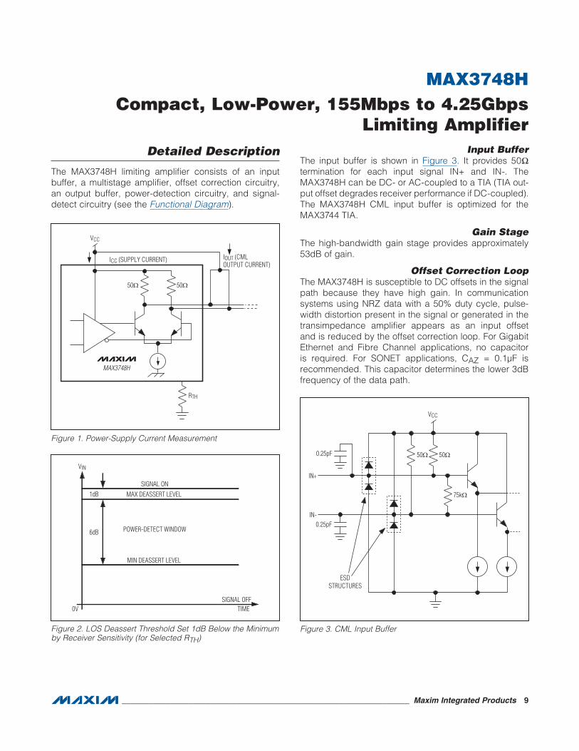
The MAX3748H limiting amplifier consists of an input buffer, a multistage amplifier, offset correction circuitry, an output buffer, power-detection circuitry, and signal-detect circuitry (see the Functional Diagram).
Input BufferThe input buffer is shown in Figure 3. It provides 50Ω termination for each input signal IN+ and IN-. The MAX3748H can be DC- or AC-coupled to a TIA (TIA out-put offset degrades receiver performance if DC-coupled). The MAX3748H CML input buffer is optimized for the MAX3744 TIA.
Gain StageThe high-bandwidth gain stage provides approximately 53dB of gain.
Offset Correction LoopThe MAX3748H is susceptible to DC offsets in the signal path because they have high gain. In communication systems using NRZ data with a 50% duty cycle, pulse-width distortion present in the signal or generated in the transimpedance amplifier appears as an input offset and is reduced by the offset correction loop. For Gigabit Ethernet and Fibre Channel applications, no capacitor is required. For SONET applications, CAZ = 0.1μF is recommended. This capacitor determines the lower 3dB frequency of the data path.
Figure 1. Power-Supply Current Measurement
Figure 2. LOS Deassert Threshold Set 1dB Below the Minimum by Receiver Sensitivity (for Selected RTH)
Figure 3. CML Input Buffer
VCC
ICC (SUPPLY CURRENT) IOUT (CML OUTPUT CURRENT)
50Ω
RTH
50Ω
MAX3748H
1dB
6dB
0V
SIGNAL ON
MAX DEASSERT LEVEL
MIN DEASSERT LEVEL
POWER-DETECT WINDOW
VIN
TIMESIGNAL OFF
50Ω 50Ω
75kΩ
IN+
IN-
0.25pF
0.25pF
VCC
ESDSTRUCTURES

Maxim Integrated Products 10
MAX3748HCompact, Low-Power, 155Mbps to 4.25Gbps
Limiting AmplifierCML Output Buffer
The MAX3748H limiting amplifier’s CML output provides high tolerance to impedance mismatches and inductive connectors. The output current is approximately 18mA. The output is disabled by connecting the DISABLE pin to VCC. If the LOS pin is connected to the DISABLE pin, the outputs OUT+ and OUT- are at a static voltage (squelch) whenever the input signal level drops below the LOS threshold. The output buffer can be AC- or DC-coupled to the load (Figure 4).
Power-Detect and Loss-of-Signal IndicatorThe MAX3748H is equipped with LOS circuitry, which indicates when the input signal is below a programmable threshold, set by resistor RTH at the TH pin (see the Typical Operating Characteristics for appropriate resis-tor sizing). An averaging peak-power detector compares the input signal amplitude with this threshold and feeds the signal detect information to the LOS output, which is open collector. Two control voltages, VASSERT and VDEASSERT, define the LOS assert and deassert levels. To prevent LOS chatter in the region of the programmed threshold, approximately 2dB of hysteresis is built into the LOS assert/deassert function. Once asserted, LOS
is not deasserted until the input amplitude rises to the required level (VDEASSERT) (Figure 5).
Design Procedure
Program the LOS Assert ThresholdExternal resistor RTH programs the LOS threshold. See the Assert/Deassert Levels vs. RTH graph in the Typical Operating Characteristics to select the appropriate resistor.
Select the Coupling CapacitorWhen AC-coupling is desired, coupling capacitors CIN and COUT should be selected to minimize the receiver’s deterministic jitter. Jitter is decreased as the input low-frequency cutoff (fIN) is decreased:
fIN = 1/[2π(50)(CIN)]
For ATM/SONET or other applications using scrambled NRZ data, select (CIN, COUT) ≥ 0.1μF, which provides fIN < 32kHz. For Fibre Channel, Gigabit Ethernet, or other applications using 8B/10B data coding, select (CIN, COUT) ≥ 0.01μF, which provides fIN < 320kHz. Refer to Application Note 292: HFAN-1.1: Choosing AC-Coupling Capacitors.
Figure 4. CML Output Buffer Figure 5. MAX3748H LOS Output Circuit
Q3 Q4 Q1
VCC
50Ω50Ω
Q2
18mA 18mA
DISABLE DISABLE
DISABLE
DATA
OUT+
OUT-
ESDSTRUCTURES
GND
ESDSTRUCTURE
VCC
LOS

Maxim Integrated Products 11
MAX3748HCompact, Low-Power, 155Mbps to 4.25Gbps
Limiting AmplifierSelect the Offset-Correction Capacitor
The capacitor between CAZ1 and CAZ2 determines the time constant of the signal path DC offset cancellation loop. To maintain stability, it is important to keep a onede-cade separation between fIN and the low-frequency cutoff (fOC) associated with the DC offset cancellation circuit. For ATM/SONET or other applications using scrambled NRZ data, fIN < 32kHz, so fOCMAX < 3.2kHz. Therefore, CAZ = 0.1μF (fOC = 2kHz). For Fibre Channel or Gigabit Ethernet applications, leave pins CAZ1 and CAZ2 open.
RSSI ImplementationThe SFF-8472 Digital Diagnostic specification requires monitoring of input receive power. The MAX3748H and MAX3744 receiver chipset allows for the monitoring of the average receive power by measuring the average DC current of the photodiode.
The MAX3744 preamp measures the average photodi-ode current and provides the information to the output common mode. The MAX3748H RSSI detect block senses the common-mode DC level of input signals IN+ and IN- and provides a ground-referenced output signal (RSSI) proportional to the photodiode current. The advantage of this implementation is that it allows the TIA to be packaged in a low-cost conventional 4-pin TO-46 header.
The MAX3748H RSSI output is connected to an analog input channel of the DS1858/DS1859 SFP controller to convert the analog information into a 16-bit word. The DS1858/DS1859 provide the receive-power information to the host board of the optical receiver through a 2-wire interface. The DS1859 allows for internal calibration of the receive-power monitor.
The MAX3744 and the MAX3748H have been optimized to achieve RSSI stability of 2.5dB within the 6μA to 500μA range of average input photodiode current. To achieve the best accuracy, Maxim recommends receive power calibration at the low end (6μA) and the high end (500μA) of the required range; see the RSSI Current Gain vs. Input TIA Current graph in the Typical Operating Characteristics.
Connecting to the DS1858/DS1859For best use of the RSSI monitor, capacitor C1 and resis-tor R1 shown in the Typical Operating Circuits (see first graphic) need to be placed as close as possible to the Maxim diagnostic monitor with the ground of C1 and R1 the same as the DS1858/DS1859 ground. Capacitor C1 suppresses system noise on the RSSI signal. R1 = 3kΩ and C1 = 0.1μF is recommended.

Maxim Integrated Products 12
MAX3748HCompact, Low-Power, 155Mbps to 4.25Gbps
Limiting AmplifierTypical Operating Circuits (continued)
MAX3744 TIA
R13kΩ
C10.1µF
IN+
IN-
THRSSI DISABLE LOS
0.1µF
OUTPOL CAZ1 CAZ2VCC
GND 4.7kΩ TO 10kΩVCC_HOST
LOS
OUT+50Ω
0.1µF
OUT-50Ω
0.1µF SerDes
RTH
SUPPLY FILTER HOST FILTER
VCC_RX5-PIN TO HEADER
HOST BOARDSFP OPTICAL RECEIVER
PIN OR APD
VCC (3.3V OR APDREFERENCE VOLTAGE)
VCC (3.3V)
MAX3748H
3-INPUT DIAGNOSTICMONITOR
DS1858
MAX3744 TIA
IN+
IN-
RSSI TH DISABLE LOS
0.1µF
OUTPOL CAZ1 CAZ2VCC
GND
LOS
OUT+50Ω
OUT-50Ω
CIN0.1µF
COUT0.1µF
COUT0.1µF
CIN0.1µF
SerDes
RTH
SUPPLY FILTER HOST FILTER
VCC_RX5-PIN TO HEADER
HOST BOARDSFP OPTICAL RECEIVER
PIN OR APD
VCC (3.3V OR APDREFERENCE VOLTAGE)
VCC (3.3V)HIGH-SIDECURRENT SENSE
MAX3748H
4.7kΩ TO 10kΩVCC_HOST
3-INPUT DIAGNOSTICMONITOR
DS1858

Maxim Integrated Products 13
MAX3748HCompact, Low-Power, 155Mbps to 4.25Gbps
Limiting AmplifierChip Information
PROCESS: SiGe BIPOLAR
Ordering Information
Package Information
For the latest package outline information and land patterns (footprints), go to www.maxim-ic.com/packages. Note that a “+”, “#”, or “-” in the package code indicates RoHS status only. Package drawings may show a different suffix character, but the drawing pertains to the package regardless of RoHS status.
+Denotes a lead(Pb)-free/RoHS-compliant package.*EP = Exposed pad.
PART TEMPRANGE PIN-PACKAGE
MAX3748HETE+ -40NC to +85NC 16 TQFN-EP* PACKAGETYPE
PACKAGECODE
OUTLINENO.
LANDPATTERNNO.
16 TQFN-EP T1633+5 21-0136 90-0031

Maxim cannot assume responsibility for use of any circuitry other than circuitry entirely embodied in a Maxim product. No circuit patent licenses are implied. Maxim reserves the right to change the circuitry and specifications without notice at any time. The parametric values (min and max limits) shown in the Electrical Characteristics table are guaranteed. Other parametric values quoted in this data sheet are provided for guidance.
Maxim Integrated Products, 120 San Gabriel Drive, Sunnyvale, CA 94086 408-737-7600 14
© 2011 Maxim Integrated Products Maxim is a registered trademark of Maxim Integrated Products, Inc.
MAX3748HCompact, Low-Power, 155Mbps to 4.25Gbps
Limiting AmplifierRevision History
REVISIONNUMBER
REVISIONDATE
DESCRIPTIONPAGES
CHANGED
0 7/11 Initial release —