MAX32620 Rev C - Maxim Integrated - Analog, linear, & … · 2017-02-13 · MAX32620 Rev C User...
689
MAX32620 Rev C User Guide AN6242; Rev 2; 02/17
Transcript of MAX32620 Rev C - Maxim Integrated - Analog, linear, & … · 2017-02-13 · MAX32620 Rev C User...

MAX32620 Rev CUser Guide
AN6242; Rev 2; 02/17

MAX32620 Rev C User Guide Contents Contents
Contents
1 Disclaimer and Revision History 1
2 Overview 2
2.1 Core and Architecture . . . . . . . . . . . . . . . . . . . . . . . . . . . . . . . . . . . . . . . . . . . . . . . . . . . . . . . . . . . . . . . . . . . 5
2.1.1 Core Parameters . . . . . . . . . . . . . . . . . . . . . . . . . . . . . . . . . . . . . . . . . . . . . . . . . . . . . . . . . . . . . . . . . 6
2.1.2 Generic Memory Map . . . . . . . . . . . . . . . . . . . . . . . . . . . . . . . . . . . . . . . . . . . . . . . . . . . . . . . . . . . . . . . 7
2.1.3 AHB Buses . . . . . . . . . . . . . . . . . . . . . . . . . . . . . . . . . . . . . . . . . . . . . . . . . . . . . . . . . . . . . . . . . . . . 8
2.1.4 APB Buses . . . . . . . . . . . . . . . . . . . . . . . . . . . . . . . . . . . . . . . . . . . . . . . . . . . . . . . . . . . . . . . . . . . . 8
2.1.5 Private Peripheral Bus (CPU Core Internal) . . . . . . . . . . . . . . . . . . . . . . . . . . . . . . . . . . . . . . . . . . . . . . . . . . . 8
2.1.6 Nested Vectored Interrupt Controller (NVIC) . . . . . . . . . . . . . . . . . . . . . . . . . . . . . . . . . . . . . . . . . . . . . . . . . . . 9
2.1.7 Debug . . . . . . . . . . . . . . . . . . . . . . . . . . . . . . . . . . . . . . . . . . . . . . . . . . . . . . . . . . . . . . . . . . . . . . . 9
2.1.8 Trace . . . . . . . . . . . . . . . . . . . . . . . . . . . . . . . . . . . . . . . . . . . . . . . . . . . . . . . . . . . . . . . . . . . . . . . 10
2.2 Power Supplies and Modes . . . . . . . . . . . . . . . . . . . . . . . . . . . . . . . . . . . . . . . . . . . . . . . . . . . . . . . . . . . . . . . . 10
2.2.1 Supply Voltages . . . . . . . . . . . . . . . . . . . . . . . . . . . . . . . . . . . . . . . . . . . . . . . . . . . . . . . . . . . . . . . . . . 10
2.2.2 VDD18 (Nominal 1.8V) Digital Power Supply . . . . . . . . . . . . . . . . . . . . . . . . . . . . . . . . . . . . . . . . . . . . . . . . . . . 10
2.2.3 VDDIO (1.8V to 3.6V) I/O Power Supply . . . . . . . . . . . . . . . . . . . . . . . . . . . . . . . . . . . . . . . . . . . . . . . . . . . . . . 10
2.2.4 VDDIOH (1.8V to 3.6V) I/O Power Supply . . . . . . . . . . . . . . . . . . . . . . . . . . . . . . . . . . . . . . . . . . . . . . . . . . . . . 11
2.2.5 VDD12 (Nominal 1.2V) Digital Power Supply . . . . . . . . . . . . . . . . . . . . . . . . . . . . . . . . . . . . . . . . . . . . . . . . . . . 11
2.2.6 VRTC (Nominal 1.8V) RTC Power Supply . . . . . . . . . . . . . . . . . . . . . . . . . . . . . . . . . . . . . . . . . . . . . . . . . . . . . 11
2.2.7 VDDA (Nominal 1.8V) Analog Power Supply . . . . . . . . . . . . . . . . . . . . . . . . . . . . . . . . . . . . . . . . . . . . . . . . . . . 11
2.2.8 VDDB (Nominal 3.3V) USB Power Supply . . . . . . . . . . . . . . . . . . . . . . . . . . . . . . . . . . . . . . . . . . . . . . . . . . . . . 11
2.2.9 Low-Power Modes . . . . . . . . . . . . . . . . . . . . . . . . . . . . . . . . . . . . . . . . . . . . . . . . . . . . . . . . . . . . . . . . 11
2.2.10 Power Supply Monitoring . . . . . . . . . . . . . . . . . . . . . . . . . . . . . . . . . . . . . . . . . . . . . . . . . . . . . . . . . . . . . 12
2.3 Clock Sources . . . . . . . . . . . . . . . . . . . . . . . . . . . . . . . . . . . . . . . . . . . . . . . . . . . . . . . . . . . . . . . . . . . . . . . 12
2.3.1 Internal 96MHz Relaxation Oscillator . . . . . . . . . . . . . . . . . . . . . . . . . . . . . . . . . . . . . . . . . . . . . . . . . . . . . . . 12
2.3.2 Internal 4MHz RC Oscillator . . . . . . . . . . . . . . . . . . . . . . . . . . . . . . . . . . . . . . . . . . . . . . . . . . . . . . . . . . . 12
Rev 2 Maxim Integrated Page i

MAX32620 Rev C User Guide Contents Contents
2.3.3 Internal 44MHz Relaxation Oscillator (Crypto Oscillator) . . . . . . . . . . . . . . . . . . . . . . . . . . . . . . . . . . . . . . . . . . . . . 12
2.3.4 RTC 32768Hz Crystal Oscillator . . . . . . . . . . . . . . . . . . . . . . . . . . . . . . . . . . . . . . . . . . . . . . . . . . . . . . . . . 13
2.4 Memory . . . . . . . . . . . . . . . . . . . . . . . . . . . . . . . . . . . . . . . . . . . . . . . . . . . . . . . . . . . . . . . . . . . . . . . . . . 13
2.4.1 Internal Flash Memory . . . . . . . . . . . . . . . . . . . . . . . . . . . . . . . . . . . . . . . . . . . . . . . . . . . . . . . . . . . . . . 13
2.4.2 8KB Instruction Cache . . . . . . . . . . . . . . . . . . . . . . . . . . . . . . . . . . . . . . . . . . . . . . . . . . . . . . . . . . . . . . 14
2.4.3 Internal SRAM . . . . . . . . . . . . . . . . . . . . . . . . . . . . . . . . . . . . . . . . . . . . . . . . . . . . . . . . . . . . . . . . . . 14
2.4.4 Peripheral Management Unit (PMU) . . . . . . . . . . . . . . . . . . . . . . . . . . . . . . . . . . . . . . . . . . . . . . . . . . . . . . . 15
2.4.5 Info Block . . . . . . . . . . . . . . . . . . . . . . . . . . . . . . . . . . . . . . . . . . . . . . . . . . . . . . . . . . . . . . . . . . . . . 15
2.4.6 Flash Memory Controller . . . . . . . . . . . . . . . . . . . . . . . . . . . . . . . . . . . . . . . . . . . . . . . . . . . . . . . . . . . . . 16
2.5 Analog Peripherals . . . . . . . . . . . . . . . . . . . . . . . . . . . . . . . . . . . . . . . . . . . . . . . . . . . . . . . . . . . . . . . . . . . . 16
2.5.1 10-Bit ADC . . . . . . . . . . . . . . . . . . . . . . . . . . . . . . . . . . . . . . . . . . . . . . . . . . . . . . . . . . . . . . . . . . . . 16
2.5.2 ADC Sample Limit Monitoring . . . . . . . . . . . . . . . . . . . . . . . . . . . . . . . . . . . . . . . . . . . . . . . . . . . . . . . . . . 16
2.6 Digital Peripherals . . . . . . . . . . . . . . . . . . . . . . . . . . . . . . . . . . . . . . . . . . . . . . . . . . . . . . . . . . . . . . . . . . . . . 16
2.6.1 GPIO Pins w/Interrupt and Wakeup Capability . . . . . . . . . . . . . . . . . . . . . . . . . . . . . . . . . . . . . . . . . . . . . . . . . . 16
2.6.2 32-Bit Timer/Counters . . . . . . . . . . . . . . . . . . . . . . . . . . . . . . . . . . . . . . . . . . . . . . . . . . . . . . . . . . . . . . 17
2.6.3 Windowed Watchdog Timers . . . . . . . . . . . . . . . . . . . . . . . . . . . . . . . . . . . . . . . . . . . . . . . . . . . . . . . . . . . 17
2.6.4 Low-Level Watchdog Timer . . . . . . . . . . . . . . . . . . . . . . . . . . . . . . . . . . . . . . . . . . . . . . . . . . . . . . . . . . . . 18
2.6.5 Real Time Clock . . . . . . . . . . . . . . . . . . . . . . . . . . . . . . . . . . . . . . . . . . . . . . . . . . . . . . . . . . . . . . . . . 18
2.6.6 SPI Masters . . . . . . . . . . . . . . . . . . . . . . . . . . . . . . . . . . . . . . . . . . . . . . . . . . . . . . . . . . . . . . . . . . . . 18
2.6.7 SPI Slave . . . . . . . . . . . . . . . . . . . . . . . . . . . . . . . . . . . . . . . . . . . . . . . . . . . . . . . . . . . . . . . . . . . . . 18
2.6.8 I2c Master . . . . . . . . . . . . . . . . . . . . . . . . . . . . . . . . . . . . . . . . . . . . . . . . . . . . . . . . . . . . . . . . . . . . . 19
2.6.9 I2c Slave . . . . . . . . . . . . . . . . . . . . . . . . . . . . . . . . . . . . . . . . . . . . . . . . . . . . . . . . . . . . . . . . . . . . . 19
2.6.10 UART . . . . . . . . . . . . . . . . . . . . . . . . . . . . . . . . . . . . . . . . . . . . . . . . . . . . . . . . . . . . . . . . . . . . . . . 19
2.6.11 USB 2.0 Device Interface with Integrated Transceiver . . . . . . . . . . . . . . . . . . . . . . . . . . . . . . . . . . . . . . . . . . . . . . 20
2.6.12 CRC Hardware Block with CRC16 and CRC32 . . . . . . . . . . . . . . . . . . . . . . . . . . . . . . . . . . . . . . . . . . . . . . . . . 20
2.7 Security Features . . . . . . . . . . . . . . . . . . . . . . . . . . . . . . . . . . . . . . . . . . . . . . . . . . . . . . . . . . . . . . . . . . . . . 20
Rev 2 Maxim Integrated Page ii

MAX32620 Rev C User Guide Contents Contents
2.7.1 Trust Protection Unit (TPU) . . . . . . . . . . . . . . . . . . . . . . . . . . . . . . . . . . . . . . . . . . . . . . . . . . . . . . . . . . . . 20
2.7.2 AES Cryptographic Engine . . . . . . . . . . . . . . . . . . . . . . . . . . . . . . . . . . . . . . . . . . . . . . . . . . . . . . . . . . . . 20
2.7.3 Secure Key Storage Area . . . . . . . . . . . . . . . . . . . . . . . . . . . . . . . . . . . . . . . . . . . . . . . . . . . . . . . . . . . . . 21
2.7.4 Code Scrambling . . . . . . . . . . . . . . . . . . . . . . . . . . . . . . . . . . . . . . . . . . . . . . . . . . . . . . . . . . . . . . . . . 21
3 Memory, Register Mapping, and Access 22
3.1 Memory, Register Mapping, and Access Overview . . . . . . . . . . . . . . . . . . . . . . . . . . . . . . . . . . . . . . . . . . . . . . . . . . . . 22
3.2 Standard Memory Regions . . . . . . . . . . . . . . . . . . . . . . . . . . . . . . . . . . . . . . . . . . . . . . . . . . . . . . . . . . . . . . . . 25
3.2.1 Code Space . . . . . . . . . . . . . . . . . . . . . . . . . . . . . . . . . . . . . . . . . . . . . . . . . . . . . . . . . . . . . . . . . . . . 25
3.2.2 SRAM Space . . . . . . . . . . . . . . . . . . . . . . . . . . . . . . . . . . . . . . . . . . . . . . . . . . . . . . . . . . . . . . . . . . . 25
3.2.3 Peripheral Space . . . . . . . . . . . . . . . . . . . . . . . . . . . . . . . . . . . . . . . . . . . . . . . . . . . . . . . . . . . . . . . . . 26
3.2.3.1 Peripheral APB Access . . . . . . . . . . . . . . . . . . . . . . . . . . . . . . . . . . . . . . . . . . . . . . . . . . . . . . . . 27
3.2.3.2 Peripheral AHB Access . . . . . . . . . . . . . . . . . . . . . . . . . . . . . . . . . . . . . . . . . . . . . . . . . . . . . . . . 28
3.2.4 External RAM Space . . . . . . . . . . . . . . . . . . . . . . . . . . . . . . . . . . . . . . . . . . . . . . . . . . . . . . . . . . . . . . . 31
3.2.5 External Device Space . . . . . . . . . . . . . . . . . . . . . . . . . . . . . . . . . . . . . . . . . . . . . . . . . . . . . . . . . . . . . . 31
3.2.6 System Area (Private Peripheral Bus) . . . . . . . . . . . . . . . . . . . . . . . . . . . . . . . . . . . . . . . . . . . . . . . . . . . . . . 31
3.2.7 System Area (Vendor Defined) . . . . . . . . . . . . . . . . . . . . . . . . . . . . . . . . . . . . . . . . . . . . . . . . . . . . . . . . . . 32
3.3 Device-Specific Memory Regions . . . . . . . . . . . . . . . . . . . . . . . . . . . . . . . . . . . . . . . . . . . . . . . . . . . . . . . . . . . . . 32
3.3.1 Instruction Cache Memory . . . . . . . . . . . . . . . . . . . . . . . . . . . . . . . . . . . . . . . . . . . . . . . . . . . . . . . . . . . . 32
3.3.2 AES Key and Working Space Memory . . . . . . . . . . . . . . . . . . . . . . . . . . . . . . . . . . . . . . . . . . . . . . . . . . . . . . 32
3.3.3 MAA Key and Working Space Memory . . . . . . . . . . . . . . . . . . . . . . . . . . . . . . . . . . . . . . . . . . . . . . . . . . . . . . 32
3.4 AHB Bus Matrix and AHB Bus Interfaces . . . . . . . . . . . . . . . . . . . . . . . . . . . . . . . . . . . . . . . . . . . . . . . . . . . . . . . . . 33
3.4.1 Core AHB Interface - I-Code . . . . . . . . . . . . . . . . . . . . . . . . . . . . . . . . . . . . . . . . . . . . . . . . . . . . . . . . . . . 33
3.4.2 Core AHB Interface - D-Code . . . . . . . . . . . . . . . . . . . . . . . . . . . . . . . . . . . . . . . . . . . . . . . . . . . . . . . . . . . 33
3.4.3 Core AHB Interface - System . . . . . . . . . . . . . . . . . . . . . . . . . . . . . . . . . . . . . . . . . . . . . . . . . . . . . . . . . . . 33
3.4.4 AHB Master - Peripheral Management Unit (PMU) . . . . . . . . . . . . . . . . . . . . . . . . . . . . . . . . . . . . . . . . . . . . . . . . 33
3.4.5 AHB Master - USB Endpoint Buffer Manager . . . . . . . . . . . . . . . . . . . . . . . . . . . . . . . . . . . . . . . . . . . . . . . . . . . 33
Rev 2 Maxim Integrated Page iii

MAX32620 Rev C User Guide Contents Contents
3.5 Flash Controller and Instruction Cache . . . . . . . . . . . . . . . . . . . . . . . . . . . . . . . . . . . . . . . . . . . . . . . . . . . . . . . . . . 34
3.5.1 Overview . . . . . . . . . . . . . . . . . . . . . . . . . . . . . . . . . . . . . . . . . . . . . . . . . . . . . . . . . . . . . . . . . . . . . 34
3.5.2 Flash Controller Operations . . . . . . . . . . . . . . . . . . . . . . . . . . . . . . . . . . . . . . . . . . . . . . . . . . . . . . . . . . . . 34
3.5.2.1 Flash Write Operation . . . . . . . . . . . . . . . . . . . . . . . . . . . . . . . . . . . . . . . . . . . . . . . . . . . . . . . . . 34
3.5.2.2 Flash Page Erase Operation . . . . . . . . . . . . . . . . . . . . . . . . . . . . . . . . . . . . . . . . . . . . . . . . . . . . . . 35
3.5.3 Instruction Cache Controller Operations . . . . . . . . . . . . . . . . . . . . . . . . . . . . . . . . . . . . . . . . . . . . . . . . . . . . . 36
3.5.3.1 Enabling the Instruction Cache . . . . . . . . . . . . . . . . . . . . . . . . . . . . . . . . . . . . . . . . . . . . . . . . . . . . 36
3.5.3.2 Flushing the Instruction Cache Contents . . . . . . . . . . . . . . . . . . . . . . . . . . . . . . . . . . . . . . . . . . . . . . . 36
3.5.4 Registers (FLC) . . . . . . . . . . . . . . . . . . . . . . . . . . . . . . . . . . . . . . . . . . . . . . . . . . . . . . . . . . . . . . . . . . 37
3.5.5 Registers (ICC) . . . . . . . . . . . . . . . . . . . . . . . . . . . . . . . . . . . . . . . . . . . . . . . . . . . . . . . . . . . . . . . . . . 62
3.5.6 Registers (TRIM) . . . . . . . . . . . . . . . . . . . . . . . . . . . . . . . . . . . . . . . . . . . . . . . . . . . . . . . . . . . . . . . . . 65
4 System Configuration and Management 69
4.1 Recommended Settings For Application Startup . . . . . . . . . . . . . . . . . . . . . . . . . . . . . . . . . . . . . . . . . . . . . . . . . . . . . 69
4.2 Power Ecosystem and Operating Modes . . . . . . . . . . . . . . . . . . . . . . . . . . . . . . . . . . . . . . . . . . . . . . . . . . . . . . . . . 71
4.2.1 Power Ecosystem . . . . . . . . . . . . . . . . . . . . . . . . . . . . . . . . . . . . . . . . . . . . . . . . . . . . . . . . . . . . . . . . . 71
4.2.2 Power Modes . . . . . . . . . . . . . . . . . . . . . . . . . . . . . . . . . . . . . . . . . . . . . . . . . . . . . . . . . . . . . . . . . . . 73
4.2.2.1 Low Power Mode 0 (LP0:STOP) . . . . . . . . . . . . . . . . . . . . . . . . . . . . . . . . . . . . . . . . . . . . . . . . . . . . 73
4.2.2.2 Low Power Mode 1 (LP1:STANDBY) . . . . . . . . . . . . . . . . . . . . . . . . . . . . . . . . . . . . . . . . . . . . . . . . . 73
4.2.2.3 Low Power Mode 2 (LP2:Peripheral Management Unit) . . . . . . . . . . . . . . . . . . . . . . . . . . . . . . . . . . . . . . . . 73
4.2.2.4 Low Power Mode 3 (LP3:RUN) . . . . . . . . . . . . . . . . . . . . . . . . . . . . . . . . . . . . . . . . . . . . . . . . . . . . 74
4.2.2.5 Wakeup Events from LP0:STOP and LP1:STANDBY . . . . . . . . . . . . . . . . . . . . . . . . . . . . . . . . . . . . . . . . . 74
4.2.3 Power State Matrix Control Options . . . . . . . . . . . . . . . . . . . . . . . . . . . . . . . . . . . . . . . . . . . . . . . . . . . . . . . 74
4.2.4 Power Ecosystem . . . . . . . . . . . . . . . . . . . . . . . . . . . . . . . . . . . . . . . . . . . . . . . . . . . . . . . . . . . . . . . . . 76
4.2.5 Supply Voltage Monitors . . . . . . . . . . . . . . . . . . . . . . . . . . . . . . . . . . . . . . . . . . . . . . . . . . . . . . . . . . . . . 77
4.2.6 Power Sequencer . . . . . . . . . . . . . . . . . . . . . . . . . . . . . . . . . . . . . . . . . . . . . . . . . . . . . . . . . . . . . . . . . 77
4.2.6.1 Power Mode Transitioning to Low Power Modes . . . . . . . . . . . . . . . . . . . . . . . . . . . . . . . . . . . . . . . . . . . . 77
Rev 2 Maxim Integrated Page iv

MAX32620 Rev C User Guide Contents Contents
4.2.7 Registers (PWRSEQ) . . . . . . . . . . . . . . . . . . . . . . . . . . . . . . . . . . . . . . . . . . . . . . . . . . . . . . . . . . . . . . . 78
4.2.8 Registers (PWRMAN) . . . . . . . . . . . . . . . . . . . . . . . . . . . . . . . . . . . . . . . . . . . . . . . . . . . . . . . . . . . . . . . 122
4.3 Interrupt Vector Table . . . . . . . . . . . . . . . . . . . . . . . . . . . . . . . . . . . . . . . . . . . . . . . . . . . . . . . . . . . . . . . . . . . 152
4.4 Resets and Reset Sources . . . . . . . . . . . . . . . . . . . . . . . . . . . . . . . . . . . . . . . . . . . . . . . . . . . . . . . . . . . . . . . . 165
4.4.1 System Reset . . . . . . . . . . . . . . . . . . . . . . . . . . . . . . . . . . . . . . . . . . . . . . . . . . . . . . . . . . . . . . . . . . . 166
4.4.1.1 System Reset Pin (SRSTN) . . . . . . . . . . . . . . . . . . . . . . . . . . . . . . . . . . . . . . . . . . . . . . . . . . . . . . 166
4.4.2 Power-On Reset (POR) . . . . . . . . . . . . . . . . . . . . . . . . . . . . . . . . . . . . . . . . . . . . . . . . . . . . . . . . . . . . . . 166
4.4.3 Power Sequencer Reset (PWRSEQ_Reset) . . . . . . . . . . . . . . . . . . . . . . . . . . . . . . . . . . . . . . . . . . . . . . . . . . . 166
4.4.3.1 RSTN (PWRSEQ_RSTN) Pin . . . . . . . . . . . . . . . . . . . . . . . . . . . . . . . . . . . . . . . . . . . . . . . . . . . . . 167
4.4.4 VRTC Power On Reset (VRTC_POR) . . . . . . . . . . . . . . . . . . . . . . . . . . . . . . . . . . . . . . . . . . . . . . . . . . . . . . 167
4.5 Device Clock Sources and Configuration . . . . . . . . . . . . . . . . . . . . . . . . . . . . . . . . . . . . . . . . . . . . . . . . . . . . . . . . . 168
4.5.1 Clock Sources . . . . . . . . . . . . . . . . . . . . . . . . . . . . . . . . . . . . . . . . . . . . . . . . . . . . . . . . . . . . . . . . . . 168
4.5.1.1 System Relaxation Oscillator (96MHz) . . . . . . . . . . . . . . . . . . . . . . . . . . . . . . . . . . . . . . . . . . . . . . . . 170
4.5.1.2 Internal RC Oscillator (4MHz) . . . . . . . . . . . . . . . . . . . . . . . . . . . . . . . . . . . . . . . . . . . . . . . . . . . . . 172
4.5.1.3 Configuring the Primary System Oscillator . . . . . . . . . . . . . . . . . . . . . . . . . . . . . . . . . . . . . . . . . . . . . . 173
4.5.1.4 Internal Crypto Oscillator (44MHz) . . . . . . . . . . . . . . . . . . . . . . . . . . . . . . . . . . . . . . . . . . . . . . . . . . . 174
4.5.1.5 32768Hz Oscillator With External Crystal . . . . . . . . . . . . . . . . . . . . . . . . . . . . . . . . . . . . . . . . . . . . . . . 174
4.5.2 Clock Configuration . . . . . . . . . . . . . . . . . . . . . . . . . . . . . . . . . . . . . . . . . . . . . . . . . . . . . . . . . . . . . . . . 175
4.5.2.1 System Clock Configuration . . . . . . . . . . . . . . . . . . . . . . . . . . . . . . . . . . . . . . . . . . . . . . . . . . . . . . 175
4.5.2.2 Cryptographic Clock Configuration . . . . . . . . . . . . . . . . . . . . . . . . . . . . . . . . . . . . . . . . . . . . . . . . . . 176
4.5.2.3 ADC Clock Configuration . . . . . . . . . . . . . . . . . . . . . . . . . . . . . . . . . . . . . . . . . . . . . . . . . . . . . . . 176
4.5.3 Registers (CLKMAN) . . . . . . . . . . . . . . . . . . . . . . . . . . . . . . . . . . . . . . . . . . . . . . . . . . . . . . . . . . . . . . . 177
4.6 Windowed Watchdog Timers . . . . . . . . . . . . . . . . . . . . . . . . . . . . . . . . . . . . . . . . . . . . . . . . . . . . . . . . . . . . . . . 213
4.6.1 Overview . . . . . . . . . . . . . . . . . . . . . . . . . . . . . . . . . . . . . . . . . . . . . . . . . . . . . . . . . . . . . . . . . . . . . 213
4.6.2 Clock Source Selection and Gating . . . . . . . . . . . . . . . . . . . . . . . . . . . . . . . . . . . . . . . . . . . . . . . . . . . . . . . . 213
4.6.3 Watchdog Timer Configuration . . . . . . . . . . . . . . . . . . . . . . . . . . . . . . . . . . . . . . . . . . . . . . . . . . . . . . . . . . 214
Rev 2 Maxim Integrated Page v

MAX32620 Rev C User Guide Contents Contents
4.6.3.1 Enabling and Disabling the Watchdog Timer Counter . . . . . . . . . . . . . . . . . . . . . . . . . . . . . . . . . . . . . . . . . 214
4.6.3.2 Locking and Unlocking the Watchdog Timer Configuration . . . . . . . . . . . . . . . . . . . . . . . . . . . . . . . . . . . . . . 215
4.6.4 Watchdog Timer Operation . . . . . . . . . . . . . . . . . . . . . . . . . . . . . . . . . . . . . . . . . . . . . . . . . . . . . . . . . . . . 215
4.6.5 Registers (WDT) . . . . . . . . . . . . . . . . . . . . . . . . . . . . . . . . . . . . . . . . . . . . . . . . . . . . . . . . . . . . . . . . . 216
4.7 Low-Level Watchdog Timer . . . . . . . . . . . . . . . . . . . . . . . . . . . . . . . . . . . . . . . . . . . . . . . . . . . . . . . . . . . . . . . . 223
4.7.1 Overview . . . . . . . . . . . . . . . . . . . . . . . . . . . . . . . . . . . . . . . . . . . . . . . . . . . . . . . . . . . . . . . . . . . . . 223
4.7.2 Clock Source and Gating . . . . . . . . . . . . . . . . . . . . . . . . . . . . . . . . . . . . . . . . . . . . . . . . . . . . . . . . . . . . . 223
4.7.3 Watchdog Timer Configuration . . . . . . . . . . . . . . . . . . . . . . . . . . . . . . . . . . . . . . . . . . . . . . . . . . . . . . . . . . 223
4.7.3.1 Enabling and Disabling the Watchdog Timer Counter . . . . . . . . . . . . . . . . . . . . . . . . . . . . . . . . . . . . . . . . . 224
4.7.3.2 Locking and Unlocking the Watchdog Timer Configuration . . . . . . . . . . . . . . . . . . . . . . . . . . . . . . . . . . . . . . 224
4.7.4 Watchdog Timer Operation . . . . . . . . . . . . . . . . . . . . . . . . . . . . . . . . . . . . . . . . . . . . . . . . . . . . . . . . . . . . 225
4.7.4.1 Configuring WDT2 to Wake Up the System from LP0 or LP1 . . . . . . . . . . . . . . . . . . . . . . . . . . . . . . . . . . . . . 225
4.7.4.2 Configuring WDT2 to Reset the Power Sequencer . . . . . . . . . . . . . . . . . . . . . . . . . . . . . . . . . . . . . . . . . . 225
4.7.5 Registers (WDT2) . . . . . . . . . . . . . . . . . . . . . . . . . . . . . . . . . . . . . . . . . . . . . . . . . . . . . . . . . . . . . . . . . 227
5 GPIO Pin Configuration and Peripheral Function Mapping 233
5.1 Pin Function Mapping . . . . . . . . . . . . . . . . . . . . . . . . . . . . . . . . . . . . . . . . . . . . . . . . . . . . . . . . . . . . . . . . . . . 233
5.1.1 GPIO Function Mapping . . . . . . . . . . . . . . . . . . . . . . . . . . . . . . . . . . . . . . . . . . . . . . . . . . . . . . . . . . . . . 234
5.2 General-Purpose I/O . . . . . . . . . . . . . . . . . . . . . . . . . . . . . . . . . . . . . . . . . . . . . . . . . . . . . . . . . . . . . . . . . . . 237
5.2.1 Device Pins . . . . . . . . . . . . . . . . . . . . . . . . . . . . . . . . . . . . . . . . . . . . . . . . . . . . . . . . . . . . . . . . . . . . 238
5.2.2 Interrupts . . . . . . . . . . . . . . . . . . . . . . . . . . . . . . . . . . . . . . . . . . . . . . . . . . . . . . . . . . . . . . . . . . . . . 238
5.2.3 Firmware Control . . . . . . . . . . . . . . . . . . . . . . . . . . . . . . . . . . . . . . . . . . . . . . . . . . . . . . . . . . . . . . . . . 239
5.2.4 Highest Resistance Pullup/Pulldown Control . . . . . . . . . . . . . . . . . . . . . . . . . . . . . . . . . . . . . . . . . . . . . . . . . . . 241
5.2.4.1 Enabling Highest Resistance Pullup Mode . . . . . . . . . . . . . . . . . . . . . . . . . . . . . . . . . . . . . . . . . . . . . . 241
5.2.4.2 Enabling Highest Resistance Pulldown Mode . . . . . . . . . . . . . . . . . . . . . . . . . . . . . . . . . . . . . . . . . . . . . 242
5.2.5 GPIO Output State Behavior During Low-Power Modes . . . . . . . . . . . . . . . . . . . . . . . . . . . . . . . . . . . . . . . . . . . . . 242
5.2.5.1 Freezing GPIO Output States During (LP3:RUN LP0:STOP LP3:RUN) Power Cycle . . . . . . . . . . . . . . . . . . . . . 242
Rev 2 Maxim Integrated Page vi

MAX32620 Rev C User Guide Contents Contents
5.2.5.2 Freezing GPIO Output States During (LP3:RUN LP1:STANDBY LP3:RUN) Power Cycle . . . . . . . . . . . . . . . . . . . 243
5.3 GPIO Pins and Peripheral Mode Functions . . . . . . . . . . . . . . . . . . . . . . . . . . . . . . . . . . . . . . . . . . . . . . . . . . . . . . . . 243
5.3.1 P0/P1 GPIO Function Options . . . . . . . . . . . . . . . . . . . . . . . . . . . . . . . . . . . . . . . . . . . . . . . . . . . . . . . . . . 244
5.3.2 P2/P3 GPIO Function Options . . . . . . . . . . . . . . . . . . . . . . . . . . . . . . . . . . . . . . . . . . . . . . . . . . . . . . . . . . 246
5.3.3 P4/P5/P6 GPIO Function Options . . . . . . . . . . . . . . . . . . . . . . . . . . . . . . . . . . . . . . . . . . . . . . . . . . . . . . . . 248
5.4 Registers (GPIO) . . . . . . . . . . . . . . . . . . . . . . . . . . . . . . . . . . . . . . . . . . . . . . . . . . . . . . . . . . . . . . . . . . . . . 250
5.5 Registers (IOMAN) . . . . . . . . . . . . . . . . . . . . . . . . . . . . . . . . . . . . . . . . . . . . . . . . . . . . . . . . . . . . . . . . . . . . 275
6 Peripheral Management Unit (PMU) 318
6.1 Overview . . . . . . . . . . . . . . . . . . . . . . . . . . . . . . . . . . . . . . . . . . . . . . . . . . . . . . . . . . . . . . . . . . . . . . . . . 318
6.2 PMU Operation . . . . . . . . . . . . . . . . . . . . . . . . . . . . . . . . . . . . . . . . . . . . . . . . . . . . . . . . . . . . . . . . . . . . . . 320
6.2.1 PMU Operation Descriptors . . . . . . . . . . . . . . . . . . . . . . . . . . . . . . . . . . . . . . . . . . . . . . . . . . . . . . . . . . . 320
6.2.2 Setup and PMU Channel Start . . . . . . . . . . . . . . . . . . . . . . . . . . . . . . . . . . . . . . . . . . . . . . . . . . . . . . . . . . 320
6.2.3 PMU Channel Arbitration . . . . . . . . . . . . . . . . . . . . . . . . . . . . . . . . . . . . . . . . . . . . . . . . . . . . . . . . . . . . . 321
6.3 PMU Descriptor Details . . . . . . . . . . . . . . . . . . . . . . . . . . . . . . . . . . . . . . . . . . . . . . . . . . . . . . . . . . . . . . . . . . 321
6.3.1 MOVE Descriptor . . . . . . . . . . . . . . . . . . . . . . . . . . . . . . . . . . . . . . . . . . . . . . . . . . . . . . . . . . . . . . . . . 321
6.3.1.1 OP_CODE . . . . . . . . . . . . . . . . . . . . . . . . . . . . . . . . . . . . . . . . . . . . . . . . . . . . . . . . . . . . . . . 322
6.3.1.2 INT . . . . . . . . . . . . . . . . . . . . . . . . . . . . . . . . . . . . . . . . . . . . . . . . . . . . . . . . . . . . . . . . . . . 322
6.3.1.3 STOP . . . . . . . . . . . . . . . . . . . . . . . . . . . . . . . . . . . . . . . . . . . . . . . . . . . . . . . . . . . . . . . . . 322
6.3.1.4 RD_SIZE, WR_SIZE . . . . . . . . . . . . . . . . . . . . . . . . . . . . . . . . . . . . . . . . . . . . . . . . . . . . . . . . . . 322
6.3.1.5 RD_INC . . . . . . . . . . . . . . . . . . . . . . . . . . . . . . . . . . . . . . . . . . . . . . . . . . . . . . . . . . . . . . . . 323
6.3.1.6 WR_INC . . . . . . . . . . . . . . . . . . . . . . . . . . . . . . . . . . . . . . . . . . . . . . . . . . . . . . . . . . . . . . . . 324
6.3.1.7 CONT . . . . . . . . . . . . . . . . . . . . . . . . . . . . . . . . . . . . . . . . . . . . . . . . . . . . . . . . . . . . . . . . . 324
6.3.1.8 TRANSFER_LENGTH . . . . . . . . . . . . . . . . . . . . . . . . . . . . . . . . . . . . . . . . . . . . . . . . . . . . . . . . . 324
6.3.1.9 WRITE_ADDRESS . . . . . . . . . . . . . . . . . . . . . . . . . . . . . . . . . . . . . . . . . . . . . . . . . . . . . . . . . . 324
6.3.1.10 READ_ADDRESS . . . . . . . . . . . . . . . . . . . . . . . . . . . . . . . . . . . . . . . . . . . . . . . . . . . . . . . . . . . 324
6.3.2 WRITE Descriptor . . . . . . . . . . . . . . . . . . . . . . . . . . . . . . . . . . . . . . . . . . . . . . . . . . . . . . . . . . . . . . . . 325
Rev 2 Maxim Integrated Page vii

MAX32620 Rev C User Guide Contents Contents
6.3.2.1 OP_CODE . . . . . . . . . . . . . . . . . . . . . . . . . . . . . . . . . . . . . . . . . . . . . . . . . . . . . . . . . . . . . . . 325
6.3.2.2 INT . . . . . . . . . . . . . . . . . . . . . . . . . . . . . . . . . . . . . . . . . . . . . . . . . . . . . . . . . . . . . . . . . . . 326
6.3.2.3 STOP . . . . . . . . . . . . . . . . . . . . . . . . . . . . . . . . . . . . . . . . . . . . . . . . . . . . . . . . . . . . . . . . . 326
6.3.2.4 WRITE_METHOD . . . . . . . . . . . . . . . . . . . . . . . . . . . . . . . . . . . . . . . . . . . . . . . . . . . . . . . . . . . 326
6.3.2.5 WRITE_ADDRESS . . . . . . . . . . . . . . . . . . . . . . . . . . . . . . . . . . . . . . . . . . . . . . . . . . . . . . . . . . 327
6.3.2.6 WRITE_VALUE . . . . . . . . . . . . . . . . . . . . . . . . . . . . . . . . . . . . . . . . . . . . . . . . . . . . . . . . . . . . 327
6.3.2.7 WRITE_MASK . . . . . . . . . . . . . . . . . . . . . . . . . . . . . . . . . . . . . . . . . . . . . . . . . . . . . . . . . . . . . 327
6.3.3 WAIT Descriptor . . . . . . . . . . . . . . . . . . . . . . . . . . . . . . . . . . . . . . . . . . . . . . . . . . . . . . . . . . . . . . . . . 327
6.3.3.1 OP_CODE . . . . . . . . . . . . . . . . . . . . . . . . . . . . . . . . . . . . . . . . . . . . . . . . . . . . . . . . . . . . . . . 328
6.3.3.2 INT . . . . . . . . . . . . . . . . . . . . . . . . . . . . . . . . . . . . . . . . . . . . . . . . . . . . . . . . . . . . . . . . . . . 328
6.3.3.3 STOP . . . . . . . . . . . . . . . . . . . . . . . . . . . . . . . . . . . . . . . . . . . . . . . . . . . . . . . . . . . . . . . . . 328
6.3.3.4 WAIT . . . . . . . . . . . . . . . . . . . . . . . . . . . . . . . . . . . . . . . . . . . . . . . . . . . . . . . . . . . . . . . . . . 329
6.3.3.5 SEL . . . . . . . . . . . . . . . . . . . . . . . . . . . . . . . . . . . . . . . . . . . . . . . . . . . . . . . . . . . . . . . . . . 329
6.3.3.6 WAIT_COUNT . . . . . . . . . . . . . . . . . . . . . . . . . . . . . . . . . . . . . . . . . . . . . . . . . . . . . . . . . . . . . 329
6.3.3.7 INT_MASK . . . . . . . . . . . . . . . . . . . . . . . . . . . . . . . . . . . . . . . . . . . . . . . . . . . . . . . . . . . . . . . 329
6.3.4 JUMP Descriptor . . . . . . . . . . . . . . . . . . . . . . . . . . . . . . . . . . . . . . . . . . . . . . . . . . . . . . . . . . . . . . . . . 337
6.3.4.1 OP_CODE . . . . . . . . . . . . . . . . . . . . . . . . . . . . . . . . . . . . . . . . . . . . . . . . . . . . . . . . . . . . . . . 338
6.3.4.2 INT . . . . . . . . . . . . . . . . . . . . . . . . . . . . . . . . . . . . . . . . . . . . . . . . . . . . . . . . . . . . . . . . . . . 338
6.3.4.3 STOP . . . . . . . . . . . . . . . . . . . . . . . . . . . . . . . . . . . . . . . . . . . . . . . . . . . . . . . . . . . . . . . . . 338
6.3.4.4 NEXT_DSC_ADDRESS . . . . . . . . . . . . . . . . . . . . . . . . . . . . . . . . . . . . . . . . . . . . . . . . . . . . . . . . 338
6.3.5 LOOP Descriptor . . . . . . . . . . . . . . . . . . . . . . . . . . . . . . . . . . . . . . . . . . . . . . . . . . . . . . . . . . . . . . . . . 338
6.3.5.1 OP_CODE . . . . . . . . . . . . . . . . . . . . . . . . . . . . . . . . . . . . . . . . . . . . . . . . . . . . . . . . . . . . . . . 339
6.3.5.2 INT . . . . . . . . . . . . . . . . . . . . . . . . . . . . . . . . . . . . . . . . . . . . . . . . . . . . . . . . . . . . . . . . . . . 339
6.3.5.3 STOP . . . . . . . . . . . . . . . . . . . . . . . . . . . . . . . . . . . . . . . . . . . . . . . . . . . . . . . . . . . . . . . . . 339
6.3.5.4 SEL . . . . . . . . . . . . . . . . . . . . . . . . . . . . . . . . . . . . . . . . . . . . . . . . . . . . . . . . . . . . . . . . . . 339
6.3.5.5 NEXT_DSC_ADDRESS . . . . . . . . . . . . . . . . . . . . . . . . . . . . . . . . . . . . . . . . . . . . . . . . . . . . . . . . 339
Rev 2 Maxim Integrated Page viii

MAX32620 Rev C User Guide Contents Contents
6.3.6 POLL Descriptor . . . . . . . . . . . . . . . . . . . . . . . . . . . . . . . . . . . . . . . . . . . . . . . . . . . . . . . . . . . . . . . . . 340
6.3.6.1 OP_CODE . . . . . . . . . . . . . . . . . . . . . . . . . . . . . . . . . . . . . . . . . . . . . . . . . . . . . . . . . . . . . . . 340
6.3.6.2 INT . . . . . . . . . . . . . . . . . . . . . . . . . . . . . . . . . . . . . . . . . . . . . . . . . . . . . . . . . . . . . . . . . . . 341
6.3.6.3 STOP . . . . . . . . . . . . . . . . . . . . . . . . . . . . . . . . . . . . . . . . . . . . . . . . . . . . . . . . . . . . . . . . . 341
6.3.6.4 AND . . . . . . . . . . . . . . . . . . . . . . . . . . . . . . . . . . . . . . . . . . . . . . . . . . . . . . . . . . . . . . . . . . 341
6.3.6.5 POLL_ADDRESS . . . . . . . . . . . . . . . . . . . . . . . . . . . . . . . . . . . . . . . . . . . . . . . . . . . . . . . . . . . 341
6.3.6.6 DATA_EXPECTED . . . . . . . . . . . . . . . . . . . . . . . . . . . . . . . . . . . . . . . . . . . . . . . . . . . . . . . . . . . 341
6.3.6.7 DATA_MASK . . . . . . . . . . . . . . . . . . . . . . . . . . . . . . . . . . . . . . . . . . . . . . . . . . . . . . . . . . . . . . 341
6.3.6.8 POLLING_INTERVAL . . . . . . . . . . . . . . . . . . . . . . . . . . . . . . . . . . . . . . . . . . . . . . . . . . . . . . . . . 341
6.3.7 BRANCH Descriptor . . . . . . . . . . . . . . . . . . . . . . . . . . . . . . . . . . . . . . . . . . . . . . . . . . . . . . . . . . . . . . . 341
6.3.7.1 OP_CODE . . . . . . . . . . . . . . . . . . . . . . . . . . . . . . . . . . . . . . . . . . . . . . . . . . . . . . . . . . . . . . . 342
6.3.7.2 INT . . . . . . . . . . . . . . . . . . . . . . . . . . . . . . . . . . . . . . . . . . . . . . . . . . . . . . . . . . . . . . . . . . . 342
6.3.7.3 STOP . . . . . . . . . . . . . . . . . . . . . . . . . . . . . . . . . . . . . . . . . . . . . . . . . . . . . . . . . . . . . . . . . 343
6.3.7.4 AND . . . . . . . . . . . . . . . . . . . . . . . . . . . . . . . . . . . . . . . . . . . . . . . . . . . . . . . . . . . . . . . . . . 343
6.3.7.5 BR_TYPE . . . . . . . . . . . . . . . . . . . . . . . . . . . . . . . . . . . . . . . . . . . . . . . . . . . . . . . . . . . . . . . 343
6.3.7.6 POLL_ADDRESS . . . . . . . . . . . . . . . . . . . . . . . . . . . . . . . . . . . . . . . . . . . . . . . . . . . . . . . . . . . 344
6.3.7.7 DATA_EXPECTED . . . . . . . . . . . . . . . . . . . . . . . . . . . . . . . . . . . . . . . . . . . . . . . . . . . . . . . . . . . 344
6.3.7.8 DATA_MASK . . . . . . . . . . . . . . . . . . . . . . . . . . . . . . . . . . . . . . . . . . . . . . . . . . . . . . . . . . . . . . 344
6.3.7.9 BRANCH_NEXT_DSC_ADDRESS . . . . . . . . . . . . . . . . . . . . . . . . . . . . . . . . . . . . . . . . . . . . . . . . . . 344
6.3.8 TRANSFER Descriptor . . . . . . . . . . . . . . . . . . . . . . . . . . . . . . . . . . . . . . . . . . . . . . . . . . . . . . . . . . . . . . 344
6.3.8.1 OP_CODE . . . . . . . . . . . . . . . . . . . . . . . . . . . . . . . . . . . . . . . . . . . . . . . . . . . . . . . . . . . . . . . 345
6.3.8.2 INT . . . . . . . . . . . . . . . . . . . . . . . . . . . . . . . . . . . . . . . . . . . . . . . . . . . . . . . . . . . . . . . . . . . 345
6.3.8.3 STOP . . . . . . . . . . . . . . . . . . . . . . . . . . . . . . . . . . . . . . . . . . . . . . . . . . . . . . . . . . . . . . . . . 345
6.3.8.4 RD_SIZE, WR_SIZE . . . . . . . . . . . . . . . . . . . . . . . . . . . . . . . . . . . . . . . . . . . . . . . . . . . . . . . . . . 346
6.3.8.5 RD_INC . . . . . . . . . . . . . . . . . . . . . . . . . . . . . . . . . . . . . . . . . . . . . . . . . . . . . . . . . . . . . . . . 346
6.3.8.6 WR_INC . . . . . . . . . . . . . . . . . . . . . . . . . . . . . . . . . . . . . . . . . . . . . . . . . . . . . . . . . . . . . . . . 347
Rev 2 Maxim Integrated Page ix

MAX32620 Rev C User Guide Contents Contents
6.3.8.7 TRANSFER_LENGTH . . . . . . . . . . . . . . . . . . . . . . . . . . . . . . . . . . . . . . . . . . . . . . . . . . . . . . . . . 347
6.3.8.8 WRITE_ADDRESS . . . . . . . . . . . . . . . . . . . . . . . . . . . . . . . . . . . . . . . . . . . . . . . . . . . . . . . . . . 347
6.3.8.9 READ_ADDRESS . . . . . . . . . . . . . . . . . . . . . . . . . . . . . . . . . . . . . . . . . . . . . . . . . . . . . . . . . . . 347
6.3.8.10 INT_MASK . . . . . . . . . . . . . . . . . . . . . . . . . . . . . . . . . . . . . . . . . . . . . . . . . . . . . . . . . . . . . . . 347
6.3.8.11 BURST_SIZE . . . . . . . . . . . . . . . . . . . . . . . . . . . . . . . . . . . . . . . . . . . . . . . . . . . . . . . . . . . . . 350
6.4 Registers (PMU) . . . . . . . . . . . . . . . . . . . . . . . . . . . . . . . . . . . . . . . . . . . . . . . . . . . . . . . . . . . . . . . . . . . . . . 351
7 Communication Peripherals 357
7.1 1-Wire Master . . . . . . . . . . . . . . . . . . . . . . . . . . . . . . . . . . . . . . . . . . . . . . . . . . . . . . . . . . . . . . . . . . . . . . . 357
7.1.1 1-Wire Master Overview . . . . . . . . . . . . . . . . . . . . . . . . . . . . . . . . . . . . . . . . . . . . . . . . . . . . . . . . . . . . . 357
7.1.1.1 References . . . . . . . . . . . . . . . . . . . . . . . . . . . . . . . . . . . . . . . . . . . . . . . . . . . . . . . . . . . . . . . 357
7.1.2 OWM Pin Configuration . . . . . . . . . . . . . . . . . . . . . . . . . . . . . . . . . . . . . . . . . . . . . . . . . . . . . . . . . . . . . . 357
7.1.3 OWM Clock Selection and Clock Gating . . . . . . . . . . . . . . . . . . . . . . . . . . . . . . . . . . . . . . . . . . . . . . . . . . . . . 358
7.1.3.1 1-Wire Time Slot Period Generation . . . . . . . . . . . . . . . . . . . . . . . . . . . . . . . . . . . . . . . . . . . . . . . . . . 359
7.1.4 1-Wire Protocol . . . . . . . . . . . . . . . . . . . . . . . . . . . . . . . . . . . . . . . . . . . . . . . . . . . . . . . . . . . . . . . . . . 359
7.1.4.1 Networking Layers . . . . . . . . . . . . . . . . . . . . . . . . . . . . . . . . . . . . . . . . . . . . . . . . . . . . . . . . . . . 360
7.1.4.2 Bus Interface (Physical Layer) . . . . . . . . . . . . . . . . . . . . . . . . . . . . . . . . . . . . . . . . . . . . . . . . . . . . . 360
7.1.4.3 Reset, Presence Detect and Data Transfer (Link Layer) . . . . . . . . . . . . . . . . . . . . . . . . . . . . . . . . . . . . . . . . 361
7.1.4.4 Reading and Writing Bits . . . . . . . . . . . . . . . . . . . . . . . . . . . . . . . . . . . . . . . . . . . . . . . . . . . . . . . 362
7.1.4.5 Standard Speed and Overdrive Speed . . . . . . . . . . . . . . . . . . . . . . . . . . . . . . . . . . . . . . . . . . . . . . . . 366
7.1.4.6 ROM Commands (Network Layer) . . . . . . . . . . . . . . . . . . . . . . . . . . . . . . . . . . . . . . . . . . . . . . . . . . . 368
7.1.5 1-Wire Operation . . . . . . . . . . . . . . . . . . . . . . . . . . . . . . . . . . . . . . . . . . . . . . . . . . . . . . . . . . . . . . . . . 374
7.1.5.1 Resetting the OWM 1-Wire Master . . . . . . . . . . . . . . . . . . . . . . . . . . . . . . . . . . . . . . . . . . . . . . . . . . 374
7.1.5.2 1-Wire Data Writes . . . . . . . . . . . . . . . . . . . . . . . . . . . . . . . . . . . . . . . . . . . . . . . . . . . . . . . . . . . 374
7.1.5.3 1-Wire Data Reads . . . . . . . . . . . . . . . . . . . . . . . . . . . . . . . . . . . . . . . . . . . . . . . . . . . . . . . . . . . 375
7.1.6 Registers (OWM) . . . . . . . . . . . . . . . . . . . . . . . . . . . . . . . . . . . . . . . . . . . . . . . . . . . . . . . . . . . . . . . . . 377
7.2 I2c . . . . . . . . . . . . . . . . . . . . . . . . . . . . . . . . . . . . . . . . . . . . . . . . . . . . . . . . . . . . . . . . . . . . . . . . . . . . . 384
Rev 2 Maxim Integrated Page x

MAX32620 Rev C User Guide Contents Contents
7.2.1 Overview . . . . . . . . . . . . . . . . . . . . . . . . . . . . . . . . . . . . . . . . . . . . . . . . . . . . . . . . . . . . . . . . . . . . . 384
7.2.2 Features . . . . . . . . . . . . . . . . . . . . . . . . . . . . . . . . . . . . . . . . . . . . . . . . . . . . . . . . . . . . . . . . . . . . . 384
7.2.3 I²C Port and Pin Configurations . . . . . . . . . . . . . . . . . . . . . . . . . . . . . . . . . . . . . . . . . . . . . . . . . . . . . . . . . . 385
7.2.4 I²C Master Operation . . . . . . . . . . . . . . . . . . . . . . . . . . . . . . . . . . . . . . . . . . . . . . . . . . . . . . . . . . . . . . . 385
7.2.5 Protocol . . . . . . . . . . . . . . . . . . . . . . . . . . . . . . . . . . . . . . . . . . . . . . . . . . . . . . . . . . . . . . . . . . . . . . 387
7.2.6 Peripheral Clock Selection and Clock Gating . . . . . . . . . . . . . . . . . . . . . . . . . . . . . . . . . . . . . . . . . . . . . . . . . . . 390
7.2.6.1 Peripheral Clock Frequency Selection . . . . . . . . . . . . . . . . . . . . . . . . . . . . . . . . . . . . . . . . . . . . . . . . . 391
7.2.7 Communication and Data Transfer . . . . . . . . . . . . . . . . . . . . . . . . . . . . . . . . . . . . . . . . . . . . . . . . . . . . . . . . 392
7.2.7.1 FIFO-Based I²C Master . . . . . . . . . . . . . . . . . . . . . . . . . . . . . . . . . . . . . . . . . . . . . . . . . . . . . . . . 392
7.2.8 I²C Interrupts . . . . . . . . . . . . . . . . . . . . . . . . . . . . . . . . . . . . . . . . . . . . . . . . . . . . . . . . . . . . . . . . . . . 393
7.2.9 Module Clock Generation . . . . . . . . . . . . . . . . . . . . . . . . . . . . . . . . . . . . . . . . . . . . . . . . . . . . . . . . . . . . . 393
7.2.10 Communication and Data Transfer . . . . . . . . . . . . . . . . . . . . . . . . . . . . . . . . . . . . . . . . . . . . . . . . . . . . . . . . 394
7.2.10.1 I²C Mailbox . . . . . . . . . . . . . . . . . . . . . . . . . . . . . . . . . . . . . . . . . . . . . . . . . . . . . . . . . . . . . . . 394
7.2.10.2 Slave Addressing . . . . . . . . . . . . . . . . . . . . . . . . . . . . . . . . . . . . . . . . . . . . . . . . . . . . . . . . . . . 395
7.2.10.3 Writing to a Single Mailbox Register . . . . . . . . . . . . . . . . . . . . . . . . . . . . . . . . . . . . . . . . . . . . . . . . . . 395
7.2.10.4 Writing to Multiple Mailbox Registers . . . . . . . . . . . . . . . . . . . . . . . . . . . . . . . . . . . . . . . . . . . . . . . . . 396
7.2.10.5 Reading from a Single Mailbox Register . . . . . . . . . . . . . . . . . . . . . . . . . . . . . . . . . . . . . . . . . . . . . . . . 397
7.2.10.6 Reading from Multiple Mailbox Registers . . . . . . . . . . . . . . . . . . . . . . . . . . . . . . . . . . . . . . . . . . . . . . . 397
7.2.11 Registers (I2CM) . . . . . . . . . . . . . . . . . . . . . . . . . . . . . . . . . . . . . . . . . . . . . . . . . . . . . . . . . . . . . . . . . 399
7.2.12 Registers (I2CS) . . . . . . . . . . . . . . . . . . . . . . . . . . . . . . . . . . . . . . . . . . . . . . . . . . . . . . . . . . . . . . . . . 412
7.3 SPIM . . . . . . . . . . . . . . . . . . . . . . . . . . . . . . . . . . . . . . . . . . . . . . . . . . . . . . . . . . . . . . . . . . . . . . . . . . . . 432
7.3.1 Overview . . . . . . . . . . . . . . . . . . . . . . . . . . . . . . . . . . . . . . . . . . . . . . . . . . . . . . . . . . . . . . . . . . . . . 432
7.3.2 SPIM Port and Pin Configurations . . . . . . . . . . . . . . . . . . . . . . . . . . . . . . . . . . . . . . . . . . . . . . . . . . . . . . . . 434
7.3.2.1 Pin Layout Configuration . . . . . . . . . . . . . . . . . . . . . . . . . . . . . . . . . . . . . . . . . . . . . . . . . . . . . . . . 434
7.3.3 Clock Selection and Configuration . . . . . . . . . . . . . . . . . . . . . . . . . . . . . . . . . . . . . . . . . . . . . . . . . . . . . . . . 436
7.3.4 Clock Gating . . . . . . . . . . . . . . . . . . . . . . . . . . . . . . . . . . . . . . . . . . . . . . . . . . . . . . . . . . . . . . . . . . . 437
Rev 2 Maxim Integrated Page xi

MAX32620 Rev C User Guide Contents Contents
7.3.5 Configuration Modes Overview . . . . . . . . . . . . . . . . . . . . . . . . . . . . . . . . . . . . . . . . . . . . . . . . . . . . . . . . . . 437
7.3.5.1 Static Configuration . . . . . . . . . . . . . . . . . . . . . . . . . . . . . . . . . . . . . . . . . . . . . . . . . . . . . . . . . . 437
7.3.5.2 Dynamic Configuration . . . . . . . . . . . . . . . . . . . . . . . . . . . . . . . . . . . . . . . . . . . . . . . . . . . . . . . . . 438
7.3.5.3 SPI Mode Selection (Clock Polarity and Phase) . . . . . . . . . . . . . . . . . . . . . . . . . . . . . . . . . . . . . . . . . . . . 438
7.3.5.4 Serial Clock . . . . . . . . . . . . . . . . . . . . . . . . . . . . . . . . . . . . . . . . . . . . . . . . . . . . . . . . . . . . . . 440
7.3.5.5 Transaction Delay . . . . . . . . . . . . . . . . . . . . . . . . . . . . . . . . . . . . . . . . . . . . . . . . . . . . . . . . . . . 441
7.3.5.6 Page Size . . . . . . . . . . . . . . . . . . . . . . . . . . . . . . . . . . . . . . . . . . . . . . . . . . . . . . . . . . . . . . . 441
7.3.6 Communication and Data Transfer . . . . . . . . . . . . . . . . . . . . . . . . . . . . . . . . . . . . . . . . . . . . . . . . . . . . . . . . 442
7.3.7 Interrupts . . . . . . . . . . . . . . . . . . . . . . . . . . . . . . . . . . . . . . . . . . . . . . . . . . . . . . . . . . . . . . . . . . . . . 444
7.3.8 Registers (SPIM) . . . . . . . . . . . . . . . . . . . . . . . . . . . . . . . . . . . . . . . . . . . . . . . . . . . . . . . . . . . . . . . . . 445
7.4 SPIS . . . . . . . . . . . . . . . . . . . . . . . . . . . . . . . . . . . . . . . . . . . . . . . . . . . . . . . . . . . . . . . . . . . . . . . . . . . . 462
7.4.1 Overview . . . . . . . . . . . . . . . . . . . . . . . . . . . . . . . . . . . . . . . . . . . . . . . . . . . . . . . . . . . . . . . . . . . . . 462
7.4.2 SPIS Port and Pin Configurations . . . . . . . . . . . . . . . . . . . . . . . . . . . . . . . . . . . . . . . . . . . . . . . . . . . . . . . . 462
7.4.3 Clock Selection and Configuration . . . . . . . . . . . . . . . . . . . . . . . . . . . . . . . . . . . . . . . . . . . . . . . . . . . . . . . . 463
7.4.4 Registers (SPIS) . . . . . . . . . . . . . . . . . . . . . . . . . . . . . . . . . . . . . . . . . . . . . . . . . . . . . . . . . . . . . . . . . 464
7.5 UART . . . . . . . . . . . . . . . . . . . . . . . . . . . . . . . . . . . . . . . . . . . . . . . . . . . . . . . . . . . . . . . . . . . . . . . . . . . 473
7.5.1 Overview . . . . . . . . . . . . . . . . . . . . . . . . . . . . . . . . . . . . . . . . . . . . . . . . . . . . . . . . . . . . . . . . . . . . . 473
7.5.2 UART I/O and Pin Configuration . . . . . . . . . . . . . . . . . . . . . . . . . . . . . . . . . . . . . . . . . . . . . . . . . . . . . . . . . 473
7.5.2.1 UART Interface Signals . . . . . . . . . . . . . . . . . . . . . . . . . . . . . . . . . . . . . . . . . . . . . . . . . . . . . . . . 473
7.5.2.2 UART 0 Pin Configurations . . . . . . . . . . . . . . . . . . . . . . . . . . . . . . . . . . . . . . . . . . . . . . . . . . . . . . 474
7.5.2.3 UART 1 Pin Configurations . . . . . . . . . . . . . . . . . . . . . . . . . . . . . . . . . . . . . . . . . . . . . . . . . . . . . . 475
7.5.2.4 UART 2 Pin Configurations . . . . . . . . . . . . . . . . . . . . . . . . . . . . . . . . . . . . . . . . . . . . . . . . . . . . . . 475
7.5.2.5 UART 3 Pin Configurations . . . . . . . . . . . . . . . . . . . . . . . . . . . . . . . . . . . . . . . . . . . . . . . . . . . . . . 476
7.5.3 UART Clock Configuration . . . . . . . . . . . . . . . . . . . . . . . . . . . . . . . . . . . . . . . . . . . . . . . . . . . . . . . . . . . . 476
7.5.3.1 UART Common Clock Basis and Scaling . . . . . . . . . . . . . . . . . . . . . . . . . . . . . . . . . . . . . . . . . . . . . . . 476
7.5.3.2 UART Clock Gating Controls (Per Instance) . . . . . . . . . . . . . . . . . . . . . . . . . . . . . . . . . . . . . . . . . . . . . . 477
Rev 2 Maxim Integrated Page xii

MAX32620 Rev C User Guide Contents Contents
7.5.4 Format and Baud Rate Selection . . . . . . . . . . . . . . . . . . . . . . . . . . . . . . . . . . . . . . . . . . . . . . . . . . . . . . . . . 478
7.5.5 Transmitting and Receiving Data . . . . . . . . . . . . . . . . . . . . . . . . . . . . . . . . . . . . . . . . . . . . . . . . . . . . . . . . . 479
7.5.6 Interrupts . . . . . . . . . . . . . . . . . . . . . . . . . . . . . . . . . . . . . . . . . . . . . . . . . . . . . . . . . . . . . . . . . . . . . 479
7.5.7 Hardware Flow Control . . . . . . . . . . . . . . . . . . . . . . . . . . . . . . . . . . . . . . . . . . . . . . . . . . . . . . . . . . . . . . 479
7.5.7.1 CTS (Clear To Send) . . . . . . . . . . . . . . . . . . . . . . . . . . . . . . . . . . . . . . . . . . . . . . . . . . . . . . . . . . 479
7.5.7.2 RTS (Ready To Send) . . . . . . . . . . . . . . . . . . . . . . . . . . . . . . . . . . . . . . . . . . . . . . . . . . . . . . . . . 480
7.5.8 Multidrop Mode Support . . . . . . . . . . . . . . . . . . . . . . . . . . . . . . . . . . . . . . . . . . . . . . . . . . . . . . . . . . . . . 480
7.5.9 Registers (UART) . . . . . . . . . . . . . . . . . . . . . . . . . . . . . . . . . . . . . . . . . . . . . . . . . . . . . . . . . . . . . . . . . 482
7.6 USB Device Interface . . . . . . . . . . . . . . . . . . . . . . . . . . . . . . . . . . . . . . . . . . . . . . . . . . . . . . . . . . . . . . . . . . . 495
7.6.1 Overview . . . . . . . . . . . . . . . . . . . . . . . . . . . . . . . . . . . . . . . . . . . . . . . . . . . . . . . . . . . . . . . . . . . . . 495
7.6.2 Operation . . . . . . . . . . . . . . . . . . . . . . . . . . . . . . . . . . . . . . . . . . . . . . . . . . . . . . . . . . . . . . . . . . . . . 495
7.6.2.1 USB Reset Definitions . . . . . . . . . . . . . . . . . . . . . . . . . . . . . . . . . . . . . . . . . . . . . . . . . . . . . . . . . 495
7.6.3 USB Endpoints . . . . . . . . . . . . . . . . . . . . . . . . . . . . . . . . . . . . . . . . . . . . . . . . . . . . . . . . . . . . . . . . . . 497
7.6.3.1 Endpoint Control Register . . . . . . . . . . . . . . . . . . . . . . . . . . . . . . . . . . . . . . . . . . . . . . . . . . . . . . . 497
7.6.3.2 Endpoint Buffer Descriptor . . . . . . . . . . . . . . . . . . . . . . . . . . . . . . . . . . . . . . . . . . . . . . . . . . . . . . . 497
7.6.4 Registers (USB) . . . . . . . . . . . . . . . . . . . . . . . . . . . . . . . . . . . . . . . . . . . . . . . . . . . . . . . . . . . . . . . . . . 499
7.7 SPI XIP . . . . . . . . . . . . . . . . . . . . . . . . . . . . . . . . . . . . . . . . . . . . . . . . . . . . . . . . . . . . . . . . . . . . . . . . . . 521
7.7.1 Overview . . . . . . . . . . . . . . . . . . . . . . . . . . . . . . . . . . . . . . . . . . . . . . . . . . . . . . . . . . . . . . . . . . . . . 521
7.7.2 SPIX Pin Configuration . . . . . . . . . . . . . . . . . . . . . . . . . . . . . . . . . . . . . . . . . . . . . . . . . . . . . . . . . . . . . . 521
7.7.3 External Memory Device Requirements for Use with SPIX . . . . . . . . . . . . . . . . . . . . . . . . . . . . . . . . . . . . . . . . . . . . 522
7.7.4 SPIX Memory . . . . . . . . . . . . . . . . . . . . . . . . . . . . . . . . . . . . . . . . . . . . . . . . . . . . . . . . . . . . . . . . . . . 522
7.7.4.1 SPIX Memory Mapping . . . . . . . . . . . . . . . . . . . . . . . . . . . . . . . . . . . . . . . . . . . . . . . . . . . . . . . . 522
7.7.4.2 SPIX External Memory Caching and Scrambling . . . . . . . . . . . . . . . . . . . . . . . . . . . . . . . . . . . . . . . . . . . 524
7.7.4.3 SPIX Memory Access . . . . . . . . . . . . . . . . . . . . . . . . . . . . . . . . . . . . . . . . . . . . . . . . . . . . . . . . . 525
7.7.4.4 Configuring SPIX Memory Access . . . . . . . . . . . . . . . . . . . . . . . . . . . . . . . . . . . . . . . . . . . . . . . . . . . 525
7.7.5 SPIX Clock Selection and Clock Gating . . . . . . . . . . . . . . . . . . . . . . . . . . . . . . . . . . . . . . . . . . . . . . . . . . . . . 526
Rev 2 Maxim Integrated Page xiii

MAX32620 Rev C User Guide Contents Contents
7.7.5.1 SPIX Protocol Format and Timing . . . . . . . . . . . . . . . . . . . . . . . . . . . . . . . . . . . . . . . . . . . . . . . . . . . 527
7.7.6 SPIX Configuration . . . . . . . . . . . . . . . . . . . . . . . . . . . . . . . . . . . . . . . . . . . . . . . . . . . . . . . . . . . . . . . . 527
7.7.7 Registers (SPIX) . . . . . . . . . . . . . . . . . . . . . . . . . . . . . . . . . . . . . . . . . . . . . . . . . . . . . . . . . . . . . . . . . 535
8 Analog to Digital Converter 543
8.1 Analog to Digital Converter Overview . . . . . . . . . . . . . . . . . . . . . . . . . . . . . . . . . . . . . . . . . . . . . . . . . . . . . . . . . . . 543
8.2 Analog to Digital Converter Architecture . . . . . . . . . . . . . . . . . . . . . . . . . . . . . . . . . . . . . . . . . . . . . . . . . . . . . . . . . 543
8.3 Analog to Digital Converter Operation . . . . . . . . . . . . . . . . . . . . . . . . . . . . . . . . . . . . . . . . . . . . . . . . . . . . . . . . . . . 545
8.3.1 Control Interface . . . . . . . . . . . . . . . . . . . . . . . . . . . . . . . . . . . . . . . . . . . . . . . . . . . . . . . . . . . . . . . . . 545
8.3.2 Using an External Reference . . . . . . . . . . . . . . . . . . . . . . . . . . . . . . . . . . . . . . . . . . . . . . . . . . . . . . . . . . . 545
8.4 Analog to Digital Converter Configuration . . . . . . . . . . . . . . . . . . . . . . . . . . . . . . . . . . . . . . . . . . . . . . . . . . . . . . . . . 545
8.4.1 Power-Up Sequence . . . . . . . . . . . . . . . . . . . . . . . . . . . . . . . . . . . . . . . . . . . . . . . . . . . . . . . . . . . . . . . 546
8.4.2 Conversion Process . . . . . . . . . . . . . . . . . . . . . . . . . . . . . . . . . . . . . . . . . . . . . . . . . . . . . . . . . . . . . . . 546
8.4.3 Peripheral Clock Configuration . . . . . . . . . . . . . . . . . . . . . . . . . . . . . . . . . . . . . . . . . . . . . . . . . . . . . . . . . . 547
8.4.4 Firmware Control of the ADC Sample Rate . . . . . . . . . . . . . . . . . . . . . . . . . . . . . . . . . . . . . . . . . . . . . . . . . . . 547
8.4.5 Power-Down Sequence . . . . . . . . . . . . . . . . . . . . . . . . . . . . . . . . . . . . . . . . . . . . . . . . . . . . . . . . . . . . . . 547
8.4.6 ADC Data Limits . . . . . . . . . . . . . . . . . . . . . . . . . . . . . . . . . . . . . . . . . . . . . . . . . . . . . . . . . . . . . . . . . 547
8.4.7 Data Value Equations . . . . . . . . . . . . . . . . . . . . . . . . . . . . . . . . . . . . . . . . . . . . . . . . . . . . . . . . . . . . . . . 550
8.5 Registers (ADC) . . . . . . . . . . . . . . . . . . . . . . . . . . . . . . . . . . . . . . . . . . . . . . . . . . . . . . . . . . . . . . . . . . . . . . 552
9 Pulse Train Engine 570
9.1 Pulse Train (PT) Engine Overview . . . . . . . . . . . . . . . . . . . . . . . . . . . . . . . . . . . . . . . . . . . . . . . . . . . . . . . . . . . . 570
9.2 Prerequisites for Use . . . . . . . . . . . . . . . . . . . . . . . . . . . . . . . . . . . . . . . . . . . . . . . . . . . . . . . . . . . . . . . . . . . 571
9.2.1 Pulse Train Register Mapping . . . . . . . . . . . . . . . . . . . . . . . . . . . . . . . . . . . . . . . . . . . . . . . . . . . . . . . . . . . 571
9.2.2 Pulse Train Peripheral Clock Generation . . . . . . . . . . . . . . . . . . . . . . . . . . . . . . . . . . . . . . . . . . . . . . . . . . . . . 572
9.2.3 Pulse Train Peripheral Clock Gating . . . . . . . . . . . . . . . . . . . . . . . . . . . . . . . . . . . . . . . . . . . . . . . . . . . . . . . 572
9.2.4 Pulse Train GPIO Mapping . . . . . . . . . . . . . . . . . . . . . . . . . . . . . . . . . . . . . . . . . . . . . . . . . . . . . . . . . . . . 573
Rev 2 Maxim Integrated Page xiv

MAX32620 Rev C User Guide Contents Contents
9.3 Pulse Train Global Controls . . . . . . . . . . . . . . . . . . . . . . . . . . . . . . . . . . . . . . . . . . . . . . . . . . . . . . . . . . . . . . . . 573
9.3.1 Enabling and Disabling Pulse Train Engines . . . . . . . . . . . . . . . . . . . . . . . . . . . . . . . . . . . . . . . . . . . . . . . . . . . 574
9.3.2 Interrupt Controls for All Pulse Train Engines . . . . . . . . . . . . . . . . . . . . . . . . . . . . . . . . . . . . . . . . . . . . . . . . . . . 574
9.3.3 Synchronizing Pulse Train Instances . . . . . . . . . . . . . . . . . . . . . . . . . . . . . . . . . . . . . . . . . . . . . . . . . . . . . . . 574
9.4 Pulse Train Engine Operation . . . . . . . . . . . . . . . . . . . . . . . . . . . . . . . . . . . . . . . . . . . . . . . . . . . . . . . . . . . . . . . 575
9.4.1 Default GPIO Output . . . . . . . . . . . . . . . . . . . . . . . . . . . . . . . . . . . . . . . . . . . . . . . . . . . . . . . . . . . . . . . 575
9.4.2 Output Rate Control . . . . . . . . . . . . . . . . . . . . . . . . . . . . . . . . . . . . . . . . . . . . . . . . . . . . . . . . . . . . . . . . 575
9.4.3 Pulse Train Mode . . . . . . . . . . . . . . . . . . . . . . . . . . . . . . . . . . . . . . . . . . . . . . . . . . . . . . . . . . . . . . . . . 575
9.4.4 Pulse Train Loop Count . . . . . . . . . . . . . . . . . . . . . . . . . . . . . . . . . . . . . . . . . . . . . . . . . . . . . . . . . . . . . . 576
9.4.5 Pulse Train Loop Delay . . . . . . . . . . . . . . . . . . . . . . . . . . . . . . . . . . . . . . . . . . . . . . . . . . . . . . . . . . . . . . 576
9.4.6 Automatic Restart Mode . . . . . . . . . . . . . . . . . . . . . . . . . . . . . . . . . . . . . . . . . . . . . . . . . . . . . . . . . . . . . 577
9.4.7 Square Wave Mode . . . . . . . . . . . . . . . . . . . . . . . . . . . . . . . . . . . . . . . . . . . . . . . . . . . . . . . . . . . . . . . . 578
9.5 Registers (PT) . . . . . . . . . . . . . . . . . . . . . . . . . . . . . . . . . . . . . . . . . . . . . . . . . . . . . . . . . . . . . . . . . . . . . . . 579
10 Timer/Counters 594
10.1 Overview . . . . . . . . . . . . . . . . . . . . . . . . . . . . . . . . . . . . . . . . . . . . . . . . . . . . . . . . . . . . . . . . . . . . . . . . . 594
10.2 Timer GPIO Mapping . . . . . . . . . . . . . . . . . . . . . . . . . . . . . . . . . . . . . . . . . . . . . . . . . . . . . . . . . . . . . . . . . . . 596
10.2.1 Configuring Timer Input Pins (32-bit Mode Only) . . . . . . . . . . . . . . . . . . . . . . . . . . . . . . . . . . . . . . . . . . . . . . . . . 597
10.2.2 Configuring Timer Output Pins (32-bit Mode Only) . . . . . . . . . . . . . . . . . . . . . . . . . . . . . . . . . . . . . . . . . . . . . . . . 598
10.3 32-bit Mode Timer Operation . . . . . . . . . . . . . . . . . . . . . . . . . . . . . . . . . . . . . . . . . . . . . . . . . . . . . . . . . . . . . . . 598
10.3.1 One-Shot Mode (Output I/O) . . . . . . . . . . . . . . . . . . . . . . . . . . . . . . . . . . . . . . . . . . . . . . . . . . . . . . . . . . . 599
10.3.2 Continuous Mode (Optional Output I/O) . . . . . . . . . . . . . . . . . . . . . . . . . . . . . . . . . . . . . . . . . . . . . . . . . . . . . 600
10.3.3 Counter Mode (Required Input I/O) . . . . . . . . . . . . . . . . . . . . . . . . . . . . . . . . . . . . . . . . . . . . . . . . . . . . . . . . 601
10.3.4 PWM Mode (Required Output I/O) . . . . . . . . . . . . . . . . . . . . . . . . . . . . . . . . . . . . . . . . . . . . . . . . . . . . . . . . 602
10.3.5 Capture Mode (Required Input I/O) . . . . . . . . . . . . . . . . . . . . . . . . . . . . . . . . . . . . . . . . . . . . . . . . . . . . . . . . 603
10.3.6 Compare Mode (Optional Output I/O) . . . . . . . . . . . . . . . . . . . . . . . . . . . . . . . . . . . . . . . . . . . . . . . . . . . . . . 605
10.3.7 Gated Mode (Required Input I/O) . . . . . . . . . . . . . . . . . . . . . . . . . . . . . . . . . . . . . . . . . . . . . . . . . . . . . . . . . 606
Rev 2 Maxim Integrated Page xv

MAX32620 Rev C User Guide Contents Contents
10.3.8 Measurement Mode (Required Input I/O) . . . . . . . . . . . . . . . . . . . . . . . . . . . . . . . . . . . . . . . . . . . . . . . . . . . . . 607
10.4 16-bit Mode Timer Operation . . . . . . . . . . . . . . . . . . . . . . . . . . . . . . . . . . . . . . . . . . . . . . . . . . . . . . . . . . . . . . . 608
10.4.1 One-Shot Mode . . . . . . . . . . . . . . . . . . . . . . . . . . . . . . . . . . . . . . . . . . . . . . . . . . . . . . . . . . . . . . . . . . 609
10.4.2 Continuous Mode . . . . . . . . . . . . . . . . . . . . . . . . . . . . . . . . . . . . . . . . . . . . . . . . . . . . . . . . . . . . . . . . . 610
10.5 Registers (TMR) . . . . . . . . . . . . . . . . . . . . . . . . . . . . . . . . . . . . . . . . . . . . . . . . . . . . . . . . . . . . . . . . . . . . . . 612
11 Real Time Clock (RTC) 622
11.1 Real Time Clock Overview . . . . . . . . . . . . . . . . . . . . . . . . . . . . . . . . . . . . . . . . . . . . . . . . . . . . . . . . . . . . . . . . 622
11.1.1 Real Time Clock Features . . . . . . . . . . . . . . . . . . . . . . . . . . . . . . . . . . . . . . . . . . . . . . . . . . . . . . . . . . . . 622
11.2 RTC Resets . . . . . . . . . . . . . . . . . . . . . . . . . . . . . . . . . . . . . . . . . . . . . . . . . . . . . . . . . . . . . . . . . . . . . . . . 622
11.3 RTC Interrupts . . . . . . . . . . . . . . . . . . . . . . . . . . . . . . . . . . . . . . . . . . . . . . . . . . . . . . . . . . . . . . . . . . . . . . . 623
11.4 RTC Configuration . . . . . . . . . . . . . . . . . . . . . . . . . . . . . . . . . . . . . . . . . . . . . . . . . . . . . . . . . . . . . . . . . . . . . 624
11.4.1 Selecting the Timer Prescale Value . . . . . . . . . . . . . . . . . . . . . . . . . . . . . . . . . . . . . . . . . . . . . . . . . . . . . . . . 624
11.4.2 Setting the RTC Timer to a Zero Starting Value . . . . . . . . . . . . . . . . . . . . . . . . . . . . . . . . . . . . . . . . . . . . . . . . . 626
11.4.3 Setting the Timer Compare Alarm(s) . . . . . . . . . . . . . . . . . . . . . . . . . . . . . . . . . . . . . . . . . . . . . . . . . . . . . . . 626
11.4.4 Starting the RTC Timer . . . . . . . . . . . . . . . . . . . . . . . . . . . . . . . . . . . . . . . . . . . . . . . . . . . . . . . . . . . . . . 626
11.5 Registers (RTCTMR) . . . . . . . . . . . . . . . . . . . . . . . . . . . . . . . . . . . . . . . . . . . . . . . . . . . . . . . . . . . . . . . . . . . 627
11.6 Registers (RTCCFG) . . . . . . . . . . . . . . . . . . . . . . . . . . . . . . . . . . . . . . . . . . . . . . . . . . . . . . . . . . . . . . . . . . . 644
12 Trust Protection Unit (TPU) 648
12.1 Registers (TPU) . . . . . . . . . . . . . . . . . . . . . . . . . . . . . . . . . . . . . . . . . . . . . . . . . . . . . . . . . . . . . . . . . . . . . . 649
12.2 Registers (AES) . . . . . . . . . . . . . . . . . . . . . . . . . . . . . . . . . . . . . . . . . . . . . . . . . . . . . . . . . . . . . . . . . . . . . . 651
13 CRC16/CRC32 Engine 662
13.1 Overview . . . . . . . . . . . . . . . . . . . . . . . . . . . . . . . . . . . . . . . . . . . . . . . . . . . . . . . . . . . . . . . . . . . . . . . . . 662
13.2 Prerequisites for Use . . . . . . . . . . . . . . . . . . . . . . . . . . . . . . . . . . . . . . . . . . . . . . . . . . . . . . . . . . . . . . . . . . . 662
13.2.1 CRC Peripheral Clock Generation . . . . . . . . . . . . . . . . . . . . . . . . . . . . . . . . . . . . . . . . . . . . . . . . . . . . . . . . 662
13.2.2 CRC Peripheral Clock Gating . . . . . . . . . . . . . . . . . . . . . . . . . . . . . . . . . . . . . . . . . . . . . . . . . . . . . . . . . . . 662
Rev 2 Maxim Integrated Page xvi

MAX32620 Rev C User Guide Contents Contents
13.3 CRC16 Operation . . . . . . . . . . . . . . . . . . . . . . . . . . . . . . . . . . . . . . . . . . . . . . . . . . . . . . . . . . . . . . . . . . . . . 663
13.3.1 Calculating CRC16-CCITT-FALSE On Big-Endian Data . . . . . . . . . . . . . . . . . . . . . . . . . . . . . . . . . . . . . . . . . . . . . 663
13.3.2 Calculating CRC16-CCITT-FALSE On Little-Endian Data . . . . . . . . . . . . . . . . . . . . . . . . . . . . . . . . . . . . . . . . . . . . 664
13.3.3 Calculating CRC16-CCITT-TRUE On Big-Endian Data . . . . . . . . . . . . . . . . . . . . . . . . . . . . . . . . . . . . . . . . . . . . . . 664
13.3.4 Calculating CRC16-CCITT-TRUE On Little-Endian Data . . . . . . . . . . . . . . . . . . . . . . . . . . . . . . . . . . . . . . . . . . . . . 664
13.4 CRC32 Operation . . . . . . . . . . . . . . . . . . . . . . . . . . . . . . . . . . . . . . . . . . . . . . . . . . . . . . . . . . . . . . . . . . . . . 665
13.4.1 Calculating CRC32 On Big-Endian Data . . . . . . . . . . . . . . . . . . . . . . . . . . . . . . . . . . . . . . . . . . . . . . . . . . . . . 665
13.4.2 Calculating CRC32 On Little-Endian Data . . . . . . . . . . . . . . . . . . . . . . . . . . . . . . . . . . . . . . . . . . . . . . . . . . . . 666
13.5 Registers (CRC) . . . . . . . . . . . . . . . . . . . . . . . . . . . . . . . . . . . . . . . . . . . . . . . . . . . . . . . . . . . . . . . . . . . . . . 667
14 Trademarks and Service Marks 671
Rev 2 Maxim Integrated Page xvii

MAX32620 Rev C User Guide Disclaimer and Revision History
1 Disclaimer and Revision History
Disclaimer
LIFE SUPPORT POLICY
MAXIM’S PRODUCTS ARE NOT DESIGNED, INTENDED OR AUTHORIZED FOR USE AS CRITICAL COMPONENTS IN LIFE SUPPORT, LIFE SUSTAINING,DEVICES OR SYSTEMS OR APPLICATIONS, INCLUDING BUT NOT LIMITED TO, NUCLEAR, TRANSPORTATION OPERATING SYSTEMS, IN WHICH THEFAILURE OF SUCH GOODS COULD REASONABLY BE EXPECTED TO RESULT IN PERSONAL INJURY, LOSS OF LIFE OR SEVERE PROPERTY OR ENVI-RONMENTAL DAMAGE WITHOUT THE EXPRESS PRIOR WRITTEN APPROVAL OF THE PRESIDENT AND GENERAL COUNSEL OF MAXIM INTEGRATEDPRODUCTS, INC.
As used herein
Life support, life sustaining devices or systems are devices which (a) are intended for surgical implant into the body, or (b) support or sustain life and whose failure toperform when properly used in accordance with instructions for use provided in the labeling can be reasonably expected to result in a significant injury to the user. Acritical component is any component in a life support device or system whose failure to perform can be reasonably expected to cause the failure of the life supportdevice or system or to affect its safety or effectiveness.
Document Disclaimer
©2016 by Maxim Integrated Products, Inc. All rights reserved. Information in this publication concerning the devices, applications, or technology described isintended to suggest possible uses and may be superseded. MAXIM INTEGRATED PRODUCTS, INC. DOES NOT ASSUME LIABILITY FOR OR PROVIDE AREPRESENTATION OF ACCURACY OF THE INFORMATION, DEVICES, OR TECHNOLOGY DESCRIBED IN THIS DOCUMENT. MAXIM ALSO DOES NOTASSUME LIABILITY FOR INTELLECTUAL PROPERTY INFRINGEMENT RELATED IN ANY MANNER TO USE OF INFORMATION, DEVICES, OR TECHNOLOGYDESCRIBED HEREIN OR OTHERWISE. The information contained within this document has been verified according to the general principles of electrical andmechanical engineering or registered trademarks of Maxim Integrated Products, Inc. All other product or service names are the property of their respective owners.
Revision History
Version Changes Date
0 Release to web for MAX32620 Rev A4. 01-11-2016
1 Release to web for MAX32620 Rev C. 10-31-2016
2 Release to web for MAX32620L flash memory variants. 02-17-2017
Rev 2 Maxim Integrated Page 1

MAX32620 Rev C User Guide Overview
2 Overview
Introduction
The MAX32620 User Guide is targeted to hardware, embedded firmware and application developers. This guide provides information on how to use and configurethe MAX32620, MAX32620L and MAX32621 memory, peripherals and registers. For ordering information, complete feature sets, package information, and electricalspecifications, refer to the MAX32620/MAX32621 data sheet.
Related Documents
• ARM Cortex-M4F Technical Reference Manual available from www.arm.com• MAX32620/MAX32621 data sheet• See the product page for additional device information and links to available design resources; these may include items such as evaluation kits, reference
designs, application notes, and device errata.
Devices Covered by This Guide
This User Guide covers functionality common to the MAX32620, the MAX32620L and MAX32621 devices. For simplicity’s sake, when the device being used isreferred to in the text, it is referred to as MAX32620, even though the text applies equally well to the MAX32620L and MAX32621.
The following functionality is specific to the MAX32621 only and is not covered in this guide:• MAA modular arithmetic accelerator• PRNG pseudo-random number generator
For details on the above MAX32621 specific topics, refer to the User Guide Supplement document for the MAX32621.
The MAX32620L is a reduced flash memory version of the MAX32620. The MAX32620L includes 1MB onboard flash memory while the MAX32620 includes 2MBonboard flash memory. All details referenced using MAX32620 apply to the MAX32620L, unless specifics are noted using MAX32620L.
Key Device Features
The MAX32620 is a low-power, mixed signal microcontroller based on the 32-bit RISC ARM Cortex-M4F (M4 plus Floating Point Unit) CPU core with a maximumoperating frequency of 96MHz.
Application code runs from an onboard internal flash memory of 2MB or 1MB, with a 256KB SRAM available for general application use. An 8KB instruction cacheimproves execution throughput, and a transparent code scrambling scheme is used to protect customer intellectual property residing in the internal flash memory.
Rev 2 Maxim Integrated Page 2

MAX32620 Rev C User Guide Overview
Additionally, a SPI Execute In Place (XIP) external memory interface allows application code and data (up to 16MB) to be accessed from an external SPI memorydevice.
Four separate low-power operating modes - LP0:STOP, LP1:STANDBY, LP2:PMU, and LP3:RUN - allow the application to dynamically balance system powerconsumption against required processing capacity during different stages of operation. In the LP0:STOP and LP1:STANDBY modes, the CPU is in Deep Sleep mode(as defined in the ARM Cortex-M4 Devices Generic User Guide) and can be awakened (returning the system to LP3:RUN) by an enabled system wakeup event. Inthe LP2:PMU mode, the CPU is in Sleep mode, and can be awakened by an enabled NVIC interrupt request. In LP3:RUN, the CPU is actively executing applicationcode. Refer to the device datasheet for details on power consumption under different low-power operating modes and peripheral configurations.
The MAX32620 includes a 10-bit sigma-delta ADC with a multiplexer front end for four external input channels (two of which are 5.5V tolerant) and six internalchannels. Dedicated divided supply input channels allow direct monitoring of onboard power supplies VDD12, VDD18, VDDB, VRTC, VDDIO and VDDIOH by the ADC. Builtin limit monitors allow converted input samples from any channel to be compared against user-configurable high and low limits, with an option to trigger an interruptand wake the CPU from the LP2:PMU low power mode if attention is required.
The MAX32620 includes a wide variety of communications and interface peripherals, including a USB 2.0 slave interface, three master SPI interfaces, one SPI slaveinterface, four UART interfaces with hardware flow control and multi-drop support, three master I2c interfaces, a 1-Wire® master interface, and a slave I2c interface.
Sixteen independent pulse train engines allow hardware generation of square wave outputs or application-defined (from 2 to 32 bits in length) repeating waveformoutputs on any GPIO pin. The application-defined waveforms from one or more pulse train engines can be synchronized, and each pulse train engine can be setto output its repeating waveform either indefinitely or for a number of iterations given by a loop counter. Any of the sixteen pulse train engines can be configured tobegin generating its waveform when another pulse train engine reaches the end of its loop count, allowing pulse train output patterns to be chained back-to-back ifneeded.
Standard debug port functionality (using the JTAG or Serial-Wire Debug interfaces) is implemented to assist with application development.
Rev 2 Maxim Integrated Page 3

MAX32620 Rev C User Guide Overview
Figure 2.1: MAX32620C Block Diagram
Rev 2 Maxim Integrated Page 4

MAX32620 Rev C User Guide Overview 2.1 Core and Architecture
2.1 Core and Architecture
32-bit RISC ARM Cortex-M4F (M4 plus Floating Point Unit) Core
The MAX32620 is based on the ARM Cortex-M4F 32-bit RISC CPU, which implements the ARMv7E-M architectural profile. The implementation of the ARMCortex-M4F core used in the MAX32620 is targeted for a maximum operating frequency of 96MHz and provides the following features.
• 32-bit data path with mixed 16-bit and 32-bit instructions (Thumb-2 instruction set)• Single cycle multiply-accumulate (MAC) with 16/32-bit multiply operations and 32/64-bit accumulate operations• DSP extensions include hardware division operation (2-12 cycles)• Extended data processing instructions for SIMD (single instruction multiple data) operations, with dual 16-bit and quad 8-bit operations• Single precision Floating Point Unit (FPU) extension for floating point arithmetic (IEEESM 754 compliant)• Memory Protection Unit (MPU) for RTOS support• Nested vectored interrupt controller (NVIC) with multiple interrupt priority levels and nested interrupt support• Byte addressable memory space (accessed using 32-bit pointers), shared by code memory, data memory, and peripheral registers• Low power, highly energy efficient core reduces power consumption• Built-in debug functionality with JTAG port and Serial-Wire (SW) Debug interface (connects to internal Debug Access Port)• Power saving Sleep and Deep Sleep modes
Rev 2 Maxim Integrated Page 5

MAX32620 Rev C User Guide Overview 2.1 Core and Architecture
2.1.1 Core Parameters
When the ARM Cortex-M4F core is included in a design, values must be selected for configurable parameters in the core. For the MAX32620 design, key ARMCortex-M4F core configuration parameters are shown below.
Parameter Value Description
NUM_IRQ 64 The NVIC on this device is configured to support a maximum of 64 device-specific interrupt vectors. Not all ofthese vectors are used on the device.
LVL_WIDTH 3 Specifies the number of bits of interrupt priority levels supported. This device uses a width of three, whichmeans there are eight interrupt priority levels supported.
MPU_PRESENT 1 The MPU (memory protection unit) is included on this device, with 8 protection regions defined.
BB_PRESENT 1 Bit-banding (memory mapped bit) operations are supported on this device.
DEBUG_LVL 3 Full debug with data matching. All debug functionality is present including data matching for watchpoint gen-eration.
TRACE_LVL 0 No trace functionality included. ITM, TPIU, ETM and HTM are not present.
RESET_ALL_REGS 1 CPU core registers are set to a known state when the device exits reset.
JTAG_PRESENT 1 This device implements the JTAG Debug Access Port.
CLKGATE_PRESENT 1 Architectural gates are included to minimize dynamic power dissipation.
FPU_PRESENT 1 This device includes Floating Point Unit (FPU) functionality.
Rev 2 Maxim Integrated Page 6

MAX32620 Rev C User Guide Overview 2.1 Core and Architecture
2.1.2 Generic Memory Map
Figure 2.2: Memory Map
Rev 2 Maxim Integrated Page 7

MAX32620 Rev C User Guide Overview 2.1 Core and Architecture
2.1.3 AHB Buses
The standard ARM Advanced High Performance Bus (AHB-Lite version) is used for several different system bus masters on the MAX32620. All buses are 32 bits inwidth.
• I-Code: Performs instruction fetches from internal code memory regions. On the MAX32620, instruction fetches from internal flash memory (and external SPIXIP memory if enabled) can be cached to improve execution throughput.
• D-Code: Performs data fetches from internal flash memory (and external SPI XIP memory if enabled); this includes literal local constant fetches. These datafetches cannot be cached, unlike instruction code fetches.
• System: Performs instruction fetch, data read/write and bit band operations on internal SRAM, and data read/write (including bit band) operations on peripher-als. Instruction and data fetches on the System bus cannot be cached. Bit band remapping is performed for data accesses to internal SRAM only; instructionfetches are not affected by bit band aliasing.
Note Bit band operations are translated internally by the CPU into a read-modify-write sequence, and so only the CPU and the debug port can read orwrite to locations using the bit banding function. The bit banding alias areas, although they are shown on the memory map, do not exist as separatelogical mapped areas, and so they cannot be accessed by other AHB masters (such as the PMU) since they do not exist at this layer.
Peripherals which require higher speed access for large data transfers have control/buffer interfaces mapped to the AHB bus in the region from address 0x4010_0000to 0x401F_FFFF. These AHB interface regions are designed to allow more rapid data transfer directly through the AHB bus, without having to go through the AHB-to-APB bridge. Unlike the peripheral registers (which are accessed through the AHB-to-APB bridge), an AHB interface region for a peripheral may be accessed in8-bit, 16-bit, or 32-bit memory widths, if the peripheral supports this. Peripherals using this type of interface include SPI master, I2c master, UART, ADC, AES, CRC,and USB.
2.1.4 APB Buses
The majority of the digital and analog peripherals on the MAX32620 are controlled by registers that are memory mapped into the standard Peripheral region, fromaddress 0x4000_0000 to 0x400F_FFFF (in the bit banding enabled region). These peripherals are connected to the CPU core using a lower-speed APB peripheralbus (connected to the System AHB-Lite bus through an AHB-to-APB bridge). This improves overall system performance by reducing the amount of time that the AHBspends waiting for slower peripherals to complete register read or write operations.
Note The APB bus supports 32-bit width access only. All access to the APB peripheral register area (from 0x4000_0000 to 0x400F_FFFF) must be 32-bitwidth only with 32-bit (4 byte) alignment. Access using 8-bit or 16-bit width to this memory region is not supported and will result in an AHB memoryfault exception (returned by the AHB-to-APB bridge interface). Bit band operations in Peripheral space are not affected by this restriction, becausethe CPU translates these accesses into 32-bit read or read-modify-write operations.
2.1.5 Private Peripheral Bus (CPU Core Internal)
The Private Peripheral Bus (PPB), which includes both AHB and APB segments, is a dedicated bus internal to the ARM CPU core. This bus is accessible by theCPU and debug port only; it cannot be accessed by other AHB masters such as the Peripheral Management Unit.
Rev 2 Maxim Integrated Page 8

MAX32620 Rev C User Guide Overview 2.1 Core and Architecture
The PPB provides access to a number of ARM Cortex-M4F core components:• ROM table containing component and device identification for use by the debugger• System Control registers• NVIC (Interrupt control)• System Timer (SysTick)• Memory Protection Unit (MPU)• Floating Point Unit (FPU)• Data Watchpoint and Trace (DWT)• Flash Patch and Breakpoint (FPB)
Note The MAX32620 does not support trace functionality, which means that the DWT component is used for watchpoints only in this implementation.
For more information on these core components, refer to the ARM technical documentation for the ARM Cortex-M4F.
There is an additional External PPB (private peripheral bus) which is a 32-bit bus based on the APB (Advanced Peripheral Bus) standard. It is intended for addingcomponents to the private peripheral bus area which are not intended for general application use, since privileged operating mode is required to access this area.The MAX32620 does not map any additional components to this bus area.
2.1.6 Nested Vectored Interrupt Controller (NVIC)
The MAX32620 includes the standard Nested Vectored Interrupt Controller (NVIC) as implemented for the ARM Cortex-M4F core. The NVIC supports high speed,deterministic interrupt response, interrupt masking and multiple interrupt sources. External interrupts support rising or falling edge trigger mode, as well as leveltriggered mode.
With the core instantiation parameters given above, the NVIC supports a maximum of 64 device-specific interrupt vectors. The MAX32620 uses interrupt vectors 0to 41. Programmable interrupt priority is supported, allowing up to eight priority levels to be used (3-bit width for priority field).
Note Some device-specific interrupt vectors may include more than one potential interrupt source, and certain device-specific interrupt vectors in the range0 .. 41 may be reserved. Refer to the Interrupt Vector Table section for more details.
2.1.7 Debug
The MAX32620 includes the standard JTAG debug engine as implemented for the ARM Cortex-M4F core. The JTAG TAP interface is supported, along with thereduced-pin-count Serial-Wire Debug Interface.
There are two JTAG TAP device addresses for the MAX32620. The address for the ARM Debug, first in the JTAG chain, is 0x4BA0_0477; the address for theMaxim Test JTAG, second in the JTAG chain, is 0x07F6_7197. The Maxim Test JTAG is intended for Maxim internal testing and characterization purposes only. It ismentioned here only to avoid confusion between it and the ARM Debug JTAG TAP, and also for reference in the event that both JTAG TAPs in the chain need to bebypassed.
Rev 2 Maxim Integrated Page 9

MAX32620 Rev C User Guide Overview 2.2 Power Supplies and Modes
Note Security restrictions enforced on the Maxim Test JTAG are similar to those enforced on the ARM Debug JTAG interface. If debug access is lockedout due to security settings, the ability of the Maxim Test JTAG to access internal device memory and peripheral registers will be locked out as well.
Standard features supported by the ARM debug engine include the ability to set up to six instruction breakpoints (as well as two data literal breakpoints and four datawatchpoints), access memory areas and peripheral registers even when the CPU is running, and pause or reset the CPU. When the CPU is in the paused state,instructions may be executed in single-step mode.
Note The debug engine is coupled to the CPU only for clocking and reset purposes. If the debug engine pauses the CPU, this does not pause otherperipherals and functions on the MAX32620, which will continue to operate normally.
2.1.8 Trace
The MAX32620 does not support application tracing or trace port functionality.
2.2 Power Supplies and Modes
2.2.1 Supply Voltages
The following digital and analog supply voltages are used by the MAX32620. These are typically provided by an external power management IC (PMIC). TheMAX32620 does not include internal regulators to derive lower-voltage external supplies from higher-voltage external power supplies; this functionality (along withbattery supply management and battery charging functions) is intended to be provided by the companion PMIC device.
Note One exception is the internal retention regulator; however, this regulator is limited to certain predefined uses relating to device state retention duringLP1:STANDBY. It cannot be used to replace any of the main external power supplies while the device is in the active modes LP2:PMU or LP3:RUN.
2.2.2 VDD18 (Nominal 1.8V) Digital Power Supply
This digital power supply is used to power the internal flash memory, comparators used for power supply monitoring, the two relaxation oscillators on the MAX32620,and certain power management and monitoring functions.
2.2.3 VDDIO (1.8V to 3.6V) I/O Power Supply
This digital power supply is used by default to power the I/O drive circuitry for all GPIO pins on the device. GPIO pins can be switched on an individual basis betweenVDDIO and the alternate GPIO supply VDDIOH.
Rev 2 Maxim Integrated Page 10

MAX32620 Rev C User Guide Overview 2.2 Power Supplies and Modes
2.2.4 VDDIOH (1.8V to 3.6V) I/O Power Supply
This digital power supply can be used as an alternate power source for the I/O drive circuitry for one or more GPIO pins on the device. The use of the VDDIOH powersupply is optional, but if used, VDDIOH must be equal to or higher than VDDIO. GPIO pins can be switched on an individual basis between VDDIO and the alternateGPIO supply VDDIOH.
2.2.5 VDD12 (Nominal 1.2V) Digital Power Supply
This digital power supply is used to power most of the digital logic on the MAX32620, including the CPU core, flash memory, SRAM, the 4MHz RC oscillator, anddigital peripherals. This is also the default power source used by the retention regulator.
2.2.6 VRTC (Nominal 1.8V) RTC Power Supply
This power supply is used to maintain functions on the MAX32620 that must continue operating under all power management modes. It is used to power the32.768kHz RTC oscillator, the 8kHz nanoring oscillator, and ’always-on’ functions including the Real Time Clock, the power sequencer, and power managementfunctions including the retention controller.
If the VRTC supply drops below the VRTC POR level, all registers and functions on the entire device will be reset, including the Real Time Clock and power sequencer.
2.2.7 VDDA (Nominal 1.8V) Analog Power Supply
This power supply is used by analog functions included in the ADC and analog front end. These analog functions include the ADC itself, analog input multiplexing,internal reference generation, and internal/external reference selection. The VDDA supply is also used by some power management functions and to generate internalcomparison reference levels used for power supply monitoring. For this reason, VDDA must always be powered, even if the ADC is not being used by the application.
2.2.8 VDDB (Nominal 3.3V) USB Power Supply
This power supply (used by the USB PHY and related functions) must be provided at the VDDB pin since the MAX32620 does not include an internal USB supplyregulator.
2.2.9 Low-Power Modes
The MAX32620 supports 4 major power modes which are user configurable to application specific needs. State-specific configuration details are stored in alwayson power domain registers that are continuously powered across all modes of operation. Firmware-controlled power gating and hardware-controlled clock gating ofperipherals allow designers to optimize system power consumption. The 4 power modes supported are LP0:STOP (with or without RTC), LP1:STANDBY (with dataretention), LP2:PMU (ARM asleep) and LP3:RUN (ARM active).
Rev 2 Maxim Integrated Page 11

MAX32620 Rev C User Guide Overview 2.3 Clock Sources
For more details on the low-power modes, refer to the Power Ecosystem and Operating Modes section.
2.2.10 Power Supply Monitoring
The MAX32620 includes a set of supply voltage monitors which compare power supply levels on the device against predefined reset thresholds. Depending onapplication requirements, these supply voltage monitors can be configured to trigger interrupts when a power supply failure is detected, or the power supply statuscan simply be monitored by application firmware using SVM event status bits. For certain power supplies, the power sequencer can be configured to trigger aPower-On Reset for the entire system when a power supply failure is detected.
For more details, refer to the Power Ecosystem and Operating Modes section.
2.3 Clock Sources
2.3.1 Internal 96MHz Relaxation Oscillator
The MAX32620 includes a high-frequency internal relaxation oscillator designed to operate at a nominal frequency of 96MHz. The output of this relaxation oscillatoris the default primary system clock source for most digital logic on the device.
The MAX32620 does not support operation from an external high-frequency crystal.
2.3.2 Internal 4MHz RC Oscillator
For applications or situations where less processing power is needed, the MAX32620 provides an 4MHz internal RC oscillator which can be used as an alternateprimary clock source. When the 4MHz RC oscillator mode is enabled, the 4MHz oscillator output is used as the primary clock source, instead of the 96MHz internalrelaxation oscillator output.
2.3.3 Internal 44MHz Relaxation Oscillator (Crypto Oscillator)
A secondary high-frequency internal relaxation oscillator, targeted to run at a nominal frequency of 44MHz, is also available. This internal relaxation oscillator is alsoknown as the Crypto Oscillator. The output of this relaxation oscillator is used as a secondary timing source for cryptographic functions in the TPU including thePRNG (MAX32621 only), the AES engine, and the MAA (MAX32621 only). This increases security and makes certain types of timing-based attacks and power-analysis-based attacks against the TPU more difficult, due to the fact that certain internal cryptographic operations are driven by this secondary, non-observableclock.
The Crypto Oscillator cannot be used as a primary system clock source; it is reserved for use by TPU functions only.
Rev 2 Maxim Integrated Page 12

MAX32620 Rev C User Guide Overview 2.4 Memory
2.3.4 RTC 32768Hz Crystal Oscillator
The MAX32620 includes a 32768Hz crystal oscillator circuit, which requires an external 32.768kHz crystal to be connected between the 32KIN and 32KOUT pins asdetailed in the MAX32620 datasheet. This oscillator is used to generate the 32768Hz clock which is used by the Real Time Clock.
An external clock source may also be used in place of the 32768Hz crystal oscillator. When using this configuration, the 32.768kHz crystal is not used. Instead,the external clock source (which must meet the electrical/timing requirements given in the datasheet) is connected to the 32KIN pin, and the 32KOUT pin is leftunconnected.
The 32768Hz clock is required in order to meet USB timing standards, because this clock is used for internal frequency calibration of the 96MHz relaxation oscillator.This means that if the application will be using the USB interface, either a 32.768kHz external crystal must be installed between the 32KIN and 32KOUT pins, or a32.768kHz external clock source must be connected to the 32KIN pin. As detailed in the MAX32620 datasheet, when a 32.768kHz external clock source is connectedto the 32KIN pin, the 32KOUT pin must be left unconnected.
When the crystal oscillator is running, the 32768Hz output clock can optionally be driven to port pin P1.7. Refer to Enabling 32768Hz Oscillator Output on P1.7 fordetails.
2.4 Memory
All memory regions on the MAX32620 (including memory-mapped register areas) are implemented in little-endian format.
2.4.1 Internal Flash Memory
The MAX32620 includes 2MB (512K x 32 bits) and the MAX32620L includes 1MB (256K x 32 bits) of internal flash memory. This internal flash memory may be usedto store application program code as well as constant static data used by application code. Locations in the internal flash memory are programmed one doubleword(32 bits) at a time. Once an internal flash memory location has been programmed, it must be erased before it can be reprogrammed to a different value.
The internal flash is divided into 256 (MAX32620) and 128 (MAX32620L) pages of 8KB (2048 x 32 bits) each. When erasing data in internal flash memory, it is notpossible to erase a single doubleword (32-bit) location independently. Instead, the flash contents may be erased either by erasing a single flash memory page at atime (page erase), or by erasing the entire internal flash memory at once (mass erase). Erased (blank) locations in the internal flash memory will always read as allones (value 0xFFFF_FFFF).
Modifications to the flash memory array (either program or erase operations) are handled by the Flash Controller (FLC).
For read access, the internal flash memory is mapped into the standard code/data space region beginning at address 0x0000_0000. The internal flash memory isaccessed via the AHB, and so 8-bit, 16-bit and 32-bit read access widths are supported.
The beginning of internal flash memory (starting at address 0x0000_0000) is also the default location for the ARM exception/interrupt vector table. Since this tablecontains initialization information (such as the reset vector address) which is required for the system to properly initialize, this table must be loaded into the internalflash memory in order for the MAX32620 to execute any application code.
Rev 2 Maxim Integrated Page 13

MAX32620 Rev C User Guide Overview 2.4 Memory
2.4.2 8KB Instruction Cache
The 8KB (2048 x 32 bits) instruction cache is used to store CPU instructions that have been recently fetched from locations in the internal flash memory (or externalSPI XIP memory, if enabled). By avoiding repeated refetches of frequently accessed code, the instruction cache helps to improve execution throughput. Instructionfetches from the ARM CPU are handled by the instruction cache, which either returns the previously cached instructions (cache hit), or fetches the requested datafrom the internal flash (cache miss) and stores it for future access. Fetches between the instruction cache and the internal flash memory go through the codedescrambler, so that the content stored in the instruction cache has already been descrambled. If the external SPI XIP flash memory interface is being used,instruction fetches from the external SPI flash memory are also cached in the same manner as instructions fetched from the internal flash memory. However, unlikecontent stored in the internal flash memory, content stored in the external SPI flash memory is not scrambled.
Code access to the internal data SRAM is not cached; for this type of access, instructions are always fetched directly from the SRAM.
When data is read from the internal flash memory (D-Code fetches, as opposed to I-Code fetches for the purposes of decoding instructions), this data is fetcheddirectly from the internal flash. This includes fetches of local constant literals that are used by certain ARM instruction op codes.
Firmware has the ability to flush the instruction cache manually at any point using the ICC_INVDT_ALL register. After code mapped into a cached instruction spaceis updated (for example, if an in-application programming modification is made to an executable area of internal flash memory or external SPI XIP flash memory),firmware must flush the cache to ensure that the latest version of the code will be accessible and that stale cache contents will not be used instead of the new flashprogrammed values.
Note By default, the instruction cache is disabled following any system reset. For proper operation, the application must explicitly enable the instructioncache following system startup. Refer to the Instruction Cache Controller Operations and Recommended Settings to be Written At ApplicationStartup sections for more details.
2.4.3 Internal SRAM
The internal SRAM on the MAX32620 is 256KB in size and has a 32-bit internal width. It is mapped into the SRAM bit-banding access region beginning at address0x2000_0000, and so it can be read and written either 8/16/32 bits at a time using the standard AHB interface, or a single bit at a time using the ARM-definedbit-band alias region (beginning at address 0x2200_0000).
The bit-banding function can only be used when the SRAM is being accessed in data space by the ARM core itself, since the ARM core handles the remapping fromthe bit-banding alias area to a read-modify-write sequence (or single read/mask/shift for a bit read function) of the standard memory area.
The SRAM can be read from or written to in data space by application firmware, and can be used for either code or data access. The SRAM is also used to hold theARM CPU stack.
The contents of the SRAM are indeterminate following initial system powerup. SRAM state is maintained during LP3:RUN, LP2:PMU, and LP1:STANDBY only.
Rev 2 Maxim Integrated Page 14

MAX32620 Rev C User Guide Overview 2.4 Memory
2.4.4 Peripheral Management Unit (PMU)
The Peripheral Management Unit (PMU) is a programmable state machine that can perform DMA operations in SRAM and control multiple peripherals without usingthe CPU, thereby significantly improving overall system power consumption in LP2:PMU. It provides flexible mechanisms to perform automatic read and/or writesequences to peripherals and areas of internal SRAM and is capable of operation in LP2:PMU and LP3:RUN power modes.
Some peripherals include dedicated memory areas and/or transmit/receive FIFOs which are mapped to the AHB bus for high-speed access. The PMU is specificallyoptimized to perform DMA data transfer operations involving these AHB-mapped memory regions. Peripheral types which provide this type of interface include:
• ADC• UART• SPI Master• I2c Master• USB (Endpoint buffers are stored in the main SRAM area)• CRC• AES• MAA (MAX32621 only)
The PMU controller can read from the internal flash memory and the external SPI XIP flash memory (if enabled). It can read from and write to the internal SRAMand any peripheral register area which can be accessed on the System bus.
2.4.5 Info Block
The flash information block (also referred to as the info block) on the MAX32620 allows production trim values and other nonvolatile information that will be writtenduring the production process (e.g., device configuration and test details / logging data) to be stored in a separate dedicated area of internal flash memory.
The mapping location for the info block is in the code space area, beginning at byte address location 0x0020_0000 (which is immediately following the highest internalflash memory address). When the info block is mapped to this memory region, it can be accessed in the same manner as the main flash. That is, it can be read fromin code space, although accesses to it are not cached under any circumstances, and its contents are not scrambled. It is possible to write to locations in the infoblock using the flash controller registers.
However, this mapping of the info block (and direct read/write access to its contents) is only intended for testing and trimming purposes during the factory productiontest sequence. Once production test of the MAX32620 has completed, a lock option setting is set in the info block to prevent future modifications to the trim andoption settings. Setting the info block lockout setting also removes the info block from the memory map, which means that the only way to view its contents after thatpoint is by reading the copies of the info block settings that have been copied into the trim shadow registers. These registers are mapped to a different area in theAPB peripheral region.
The flash controller automatically copies trim and configuration settings from the info block to the trim shadow registers following power on reset (POR). For mostof these, once they are copied to the trim shadow registers, the settings will take effect automatically. However, there are a small number of settings which need tobe copied manually by firmware from the trim shadow registers into the proper trim register locations. For more details, refer to the Critical Settings for ApplicationStartup section.
Rev 2 Maxim Integrated Page 15

MAX32620 Rev C User Guide Overview 2.5 Analog Peripherals
2.4.6 Flash Memory Controller
The flash memory controller on the MAX32620 handles control and timing signals for programming and erase operations on both the internal flash memory and theinfo block. The info block is normally written during production test only, and is not generally intended to be modified by the user application.
Functions provided by the flash controller for general use by application firmware include:• Mass erase of the entire internal flash memory• Page erase of a single 8KB page in the internal flash memory• Write to a blank location (programmed 32 bits at a time) in the internal flash memory
Once a location in internal flash memory has been programmed, it cannot be reprogrammed to a different value without first erasing the entire flash page whichcontains that location.
2.5 Analog Peripherals
2.5.1 10-Bit ADC
The MAX32620 includes a 10-bit sigma-delta analog-to-digital converter (ADC) with four external analog inputs and additional analog input channels to measureinternal power supply levels. The ADC also includes an internal reference voltage generator and a high impedance input buffer.
The ADC voltage reference can be generated from either an internal or external reference voltage. Two of the external analog inputs can be configured to divide theinput voltage by five before samples are converted by the ADC.
2.5.2 ADC Sample Limit Monitoring
An optional feature allows samples captured by the ADC to be automatically compared against user-programmable high and low limits. Up to four channel limit pairscan be configured in this way. The comparison allows the ADC to trigger an interrupt when a captured sample goes outside the preprogrammed limit range. Sincethis comparison is performed directly by the sample limit monitors, it can be performed even while the main CPU is suspended in low power mode LP2:PMU.
2.6 Digital Peripherals
2.6.1 GPIO Pins w/Interrupt and Wakeup Capability
The MAX32620 includes seven GPIO ports with eight pins per port (for P0 through P5; P6 has only one GPIO pin) for a total of 49 GPIO pins.
Pins may be multiplexed with one or more digital peripheral functions. GPIO pins may be individually switched between GPIO and alternate peripheral input/outputfunctions using the appropriate control registers.
Rev 2 Maxim Integrated Page 16

MAX32620 Rev C User Guide Overview 2.6 Digital Peripherals
All GPIO pins can be configured individually by firmware to act as external interrupt sources. All GPIO pins also have the option (which is separate from configuringa GPIO pin to act as an external interrupt source) to be configured to act as wakeup sources.
All GPIO pins support standard I/O operating modes including buffered logic inputs, high impedance, weak pullup and pulldown modes, open drain, and standarddrive high/low outputs. The MAX32620 supports two different voltage supplies (VDDIO and VDDIOH) which can be used for driving GPIO outputs and referencing GPIOinput values. As noted in the datasheet, the voltage at VDDIOH must be greater than or equal to the voltage at VDDIO. Each GPIO pin can be set individually to operatefrom either of these two I/O supply voltages.
Use of VDDIOH as an alternate GPIO voltage supply is optional; if this functionality is not needed, both VDDIO and VDDIOH may be driven by the same external supplyvoltage.
2.6.2 32-Bit Timer/Counters
The MAX32620 includes six 32-bit timer/counter peripherals with the following features:• 32-bit up count with auto reload mode• One-shot or continuous operation mode• Independent prescaler for each timer peripheral allows its timer input clock to be scaled from (sys_clk_main / 1) to (sys_clk_main / 4096)• PWM output generation mode• Capture/compare modes• Input pin for counter input, clock gating, measurement mode or capture, limited to an input frequency of 1/4 of the timer input clock• Multiple GPIO input/output connection options for each timer peripheral• Timer interrupt
Each 32-bit timer/counter module also has the option to be split into two separate 16-bit timers (dual 16-bit timer mode) for a possible total of twelve 16-bit timers.When a 32-bit timer is split into a pair of 16-bit timers, the 16-bit timers have the following features:
• 16-bit up count with auto reload mode• One-shot or continuous operation mode• Prescaler (shared by both timers in the pair) allows the timer input clock to be scaled from (sys_clk_main / 1) to (sys_clk_main / 4096)• Timer interrupt (separate interrupt for each 16-bit timer in the pair)
2.6.3 Windowed Watchdog Timers
The MAX32620 includes two independent watchdog timers (WDT) with window support. The watchdog timers run independently from each other and the CPU andhave multiple clock source options for ensuring system stability. The watchdog uses a 32-bit timer with prescaler to generate the watchdog reset. When enabled, thewatchdog timers must be fed/reset prior to timeout or within a specified window of time if window mode is enabled. Failure to do so before the watchdog times outwill result in a watchdog reset event.
The first watchdog instance (WDT0) can be configured to trigger a system reset (reset of digital core) when it generates a watchdog reset. The second watchdoginstance (WDT1) can be configured to generate a system reboot (equivalent to digital POR event) when it generates a watchdog reset.
Rev 2 Maxim Integrated Page 17

MAX32620 Rev C User Guide Overview 2.6 Digital Peripherals
Multiple clock sources are available for each watchdog timer and can be independently configured using system manager settings.
2.6.4 Low-Level Watchdog Timer
In addition to the two standard watchdog timers, the MAX32620 also includes a low-level watchdog timer which can be used to reset the system to a known stateeven in extreme circumstances.
Unlike the other two watchdogs, the low-level watchdog (WDT2) is not intended to meet precise timing requirements. It has a single clock source option only (theapproximately 8kHz nano-ring oscillator) and it can be set up to run even during LP1:STANDBY or LP0:STOP modes.
The WDT2 watchdog timeout can be configured to reset the system to a known state by triggering a power sequencer reset, similar to the effects of driving the RSTNinput pin low. It is also possible for the WDT2 watchdog timeout to wake up the system from a low-power LP1:STANDBY or LP0:STOP state by triggering a full powersequencer reset (similar to the power sequencer reset that occurs when the device goes through a ’first boot’ event).
2.6.5 Real Time Clock
The real-time clock (RTC) records the date/time using a nonvolatile (powered by VRTC) 32-bit seconds counter with configurable LSB resolution determined by aprogrammable prescaler. Two time-of-day (counter comparison) alarms and an independent sub-second (interval) alarm can be configured to trigger interrupts and/orwake the device from low-power LP0:STOP, LP1:STANDBY or LP2:PMU modes.
The sub-second alarm triggers repeatedly at a configurable interval, which allows the application to define a custom timer-based event loop (the minimum intervalis 244 microseconds). This alarm can also be used to create an additional timer that can be used to measure long durations (more precisely than the main 32-bitseconds counter would allow) without performance degradation.
2.6.6 SPI Masters
The MAX32620 includes three SPI master peripherals. Each SPI master provides an independent master-mode-only serial communication channel that communi-cates synchronously with peripheral devices in a single or multiple slave system.
The SPI masters support single data line communications (half-duplex or full-duplex mode), dual data line (half-duplex only) or quad data line (half-duplex only)modes. Each SPI master also supports configuration of active SS state (active low or active high). The PMU can be used to access both the transmit (transaction)and receive FIFO buffers.
2.6.7 SPI Slave
The MAX32620 includes one SPI slave peripheral. This SPI slave supports single data line communications (half-duplex or full-duplex mode), dual data line (half-duplex only) or quad data line (half-duplex only) modes. The PMU can be used to access the TX and RX SPI Slave FIFO buffers.
Rev 2 Maxim Integrated Page 18

MAX32620 Rev C User Guide Overview 2.6 Digital Peripherals
2.6.8 I2c Master
The MAX32620 includes three I2c bus master peripherals which can be used to communicate with a wide variety of other I2c-enabled slave devices. The I2c bus isa two-wire, bidirectional bus which includes a ground line and two bus lines: the serial data line (SDA) and the serial clock line (SCL). Both the SDA and SCL linesmust be driven as open-collector/drain outputs. External resistors are required to pull the lines to a logic-high state.
The I2c master interface has ownership of the I2c bus, drives the clock, and generates the START and STOP conditions. This allows the I2c bus master to send datato a slave or receive data from a slave as required.
The I2c bus master peripherals support standard and fast mode I2c data rates. Refer to the device datasheet for signal timing details.
2.6.9 I2c Slave
The MAX32620 also includes a single I2c slave interface peripheral which acts as an I2c bus slave device.
Unlike the general-purpose FIFO-based I2c master interface, the I2c slave handles not only the low-level timing and protocol required to communicate with the I2cbus, but it also implements a set of predefined commands which allow an external I2c bus master to read and write from a set of bidirectional "mailbox" byte registers.This protocol handling is performed automatically by the I2c slave, without requiring any intervention on the part of the MAX32620 CPU.
The I2c slave relies on an externally generated SCL clock and responds to data and commands only when requested by the external I2c bus master.
The I2c slave interface peripheral supports standard and fast mode I2c data rates. Refer to the device datasheet for signal timing details.
2.6.10 UART
The MAX32620 includes four UART interface peripherals. The UART interface supports full-duplex asynchronous data transfers, and also provides optional hardwareflow control using the RTS and CTS signal lines.
Options supported by each UART interface peripheral include:• Hardware flow control using RTS (Ready to Send), CTS (Clear to Send), or both• 32-byte transmit and receive FIFOs• Programmable interrupts for receive and transmit• Independent baud rate generator• Character sizes of 5, 6, 7, or 8 bits• Configurable optional parity bit for even or odd parity checking• Optional multidrop (single master, multiple slave) mode using parity bit to mark slave address characters
Rev 2 Maxim Integrated Page 19

MAX32620 Rev C User Guide Overview 2.7 Security Features
2.6.11 USB 2.0 Device Interface with Integrated Transceiver
The MAX32620 includes a USB device controller module which is compliant with the USB 2.0 specification, providing full-speed operation as a USB peripheraldevice. The USB module includes an integrated PHY interface, which allows the external USB pins to be connected directly to the USB bus. This reduces requiredboard space and overall system cost.
The USB module includes an integrated AHB bus master which is used to write to and read from the buffers for each supported/active endpoint. These buffers arelocated in the standard system SRAM (in user-configurable locations), so they can be accessed by firmware directly as well as by the USB DMA engine. A total ofseven endpoint buffers are supported with configurable selection of IN or OUT (endpoints 1 through 7). Endpoint 0 is read-only.
2.6.12 CRC Hardware Block with CRC16 and CRC32
A CRC hardware module is included to provide fast calculations and integrity checking of application software and data. The CRC module supports both CRC16-CCITT and CRC32 polynomial modes. Both the CRC16 and CRC32 operations (per 4 bytes of data loaded) complete in a single system clock cycle.
Additional features of the CRC module include:• Programmable start seed (init value) for CRC16 mode• Programmable start seed (init value) for CRC32 mode• Selectable little-endian or big-endian byte ordering when loading input data using 16-bit or 32-bit write operations• Two predefined mode sets select options for input and output data reflection and output data inversion (equivalent to output XOR of 0xFFFF_FFFF)• Input data can be loaded directly by application firmware or automatically using the PMU
2.7 Security Features
2.7.1 Trust Protection Unit (TPU)
The MAX32620 includes several types of cryptographic and security peripherals which are grouped together to form the Trust Protection Unit, or TPU. Dependingon the device configuration, the TPU may include cryptographic peripherals (such as the AES engine or the MAA) as well as other security features (such as thePRNG). These peripherals and features can be used by applications to protect critical user information within the device.
2.7.2 AES Cryptographic Engine
One component found in the TPU is an Advanced Encryption Standard (AES) cryptographic engine. This cryptographic engine performs 256-bit AES encryption anddecryption operations in hardware with no CPU intervention required.
The AES control register selects encryption or decryption mode, controls interrupt notification of the processor upon a completion of an operation, and selectswhether or not the key expansion (generation of first/last round key) is performed before the encryption or decryption operation begins. For multiple-block encryption
Rev 2 Maxim Integrated Page 20

MAX32620 Rev C User Guide Overview 2.7 Security Features
or decryption operations using a single key, the key expansion is performed on the first block only. This allows subsequent operations of the same type using thesame key to complete more quickly by reusing the previously generated round key information.
The working AES key, cryptographic working space, and input and output parameters (plaintext to ciphertext or vice versa) are stored in a dedicated internal AESmemory. AES key memory is write-only; it is written using the AHB bus, but all reads from the AES key memory return zero.
2.7.3 Secure Key Storage Area
A 128-bit AES master key (or other critical data) can be stored in the register-based Secure Key Storage area. This area consists of four 32-bit ’always on’ registersin the RTC module. These registers will be cleared automatically when a POR occurs on the VRTC supply; they can also be cleared directly by the application at anypoint.
One potential use of the Secure Key Storage area is to hold a 128-bit master AES key. This master key, which can be generated by the device using a pseudo-randomnumber algorithm, would be intended for use in encrypting other sensitive information on the device (stored in the SRAM or the internal flash memory) that will notbe automatically cleared in the event of a POR. However, if this sensitive information has been encrypted before storage using an AES master key (which is kept inthe Secure Key Storage), then once the AES master key is cleared, any sensitive information which was encrypted by that AES master key is unrecoverable. Even ifthe ciphertext version of the information can be recovered by an external attacker in some way, the key that was used to encrypt that data will no longer exist.
Another potential use of this key would be to encrypt larger keys that might be stored in long-term, nonvolatile storage on the device (such as a public key, privatekey, or certificate, which might be stored in internal flash memory). Once the larger keys have been encrypted with the AES master key, they may safely be stored inthe main SRAM or internal flash memory.
The Secure Key Storage area does not necessarily have to be used for an AES master key; it can be used to hold any type of application-critical data.
The four VRTC-backed 32-bit registers that make up the Secure Key Storage Area are TPU_SKS0, TPU_SKS1, TPU_SKS2, and TPU_SKS3.
2.7.4 Code Scrambling
All application code and data loaded into the internal flash memory is scrambled in both content and location by hardware before it is stored in the flash. When datais retrieved from the flash, it is descrambled before arriving at the program cache (for instruction fetches) or the main data bus (for data fetches). Both the scramblingand descrambling operations are transparent to the end user.
Rev 2 Maxim Integrated Page 21

MAX32620 Rev C User Guide Memory, Register Mapping, and Access
3 Memory, Register Mapping, and Access
3.1 Memory, Register Mapping, and Access Overview
The ARM Cortex-M4F architecture defines a standard memory space for unified code and data access. This memory space is addressed in units of single bytes butis most typically accessed in 32-bit (4 byte) units. It may also be accessed, depending on the implementation, in 8-bit (1 byte) or 16-bit (2 byte) widths.
The maximum range of the memory space in the ARM Cortex-M4F architecture is 32 bits in width (4GB addressable total), from byte address 0x0000_0000 to0xFFFF_FFFF. It is important to note, however, that the architectural definition does not require the entire 4GB memory range to be populated with addressablememory instances. For example, the internal memory included on the MAX32620 only covers specific portions of the total addressable memory space, as shownbelow.
All memory regions on the MAX32620 (including memory-mapped register areas) are implemented in little-endian format.
Rev 2 Maxim Integrated Page 22

MAX32620 Rev C User Guide Memory, Register Mapping, and Access 3.1 Memory, Register Mapping, and Access Overview
Figure 3.1: Code Memory Mapping
Rev 2 Maxim Integrated Page 23

MAX32620 Rev C User Guide Memory, Register Mapping, and Access 3.1 Memory, Register Mapping, and Access Overview
Figure 3.2: Data Memory Mapping
Rev 2 Maxim Integrated Page 24

MAX32620 Rev C User Guide Memory, Register Mapping, and Access 3.2 Standard Memory Regions
3.2 Standard Memory Regions
A number of standard memory regions are defined for the ARM Cortex-M4F architecture; the use of many of these is optional for the system integrator. At aminimum, the MAX32620, a ARM Cortex-M4F-based device, must contain some code and data memory for application code and variable/stack use, as well ascertain components which are part of the instantiated core.
3.2.1 Code Space
The code space area of memory is designed to contain the primary memory used for code execution by the device. Two different standard core bus masters areused by the ARM Cortex-M4F CPU core and ARM debugger to access this memory area. The I-Code AHB bus master is used for instruction decode fetching fromcode memory, while the D-Code AHB bus master is used for data fetches from code memory. This is arranged so that data fetches avoid interfering with instructionexecution.
The code space memory area contains the 2MB (MAX32620) or 1MB (MAX32620L) main internal flash memory, which typically holds the primary instruction codethat will be executed on the device. The internal flash memory is mapped into both code and data space as shown below.
Device START ADDRESS END ADDRESS
MAX32620 0x0000_0000 0x001F_FFFF
MAX32620L 0x0000_0000 0x000F_FFFF
This program memory area must also contain the system vector table (located by default at address 0x0000_0000), which contains the reset vector for the deviceand entry point addresses for all system exception handlers and interrupt handlers.
The code space memory on the MAX32620 also contains the mapping for the info block, from 0x0020_0000 to 0x0020_1FFF. However, this mapping is generallyonly present during production test; it is disabled once the info block has been loaded with valid data and the info block lockout option has been set. This memory isaccessible for data reads only and cannot be used for code execution.
Optionally, the SPI XIP (Execute In Place) peripheral can be used to expand the available code and data memory space for the MAX32620. This expansion consistsof mapping the contents of an external SPI flash memory device (up to 16MB) into a read-only area of the code memory map. If enabled, the external memory ismapped starting at byte address 0x1000_0000 up to a maximum of 0x10FF_FFFF (for a 16MB device). This external memory can be used for code execution as wellas static data storage.
3.2.2 SRAM Space
The SRAM area of memory is intended to contain the primary SRAM data memory of the device. This memory can be used for general purpose variable and datastorage, code execution, and the ARM Cortex-M4F stack.
Rev 2 Maxim Integrated Page 25

MAX32620 Rev C User Guide Memory, Register Mapping, and Access 3.2 Standard Memory Regions
On the MAX32620, this memory area contains the 256KB SRAM, which is mapped from 0x2000_0000 to 0x2003_FFFF. The entirety of the SRAM memory spaceon the MAX32620 is contained within the dedicated ARM Cortex-M4F SRAM bit-banding region beginning at byte address 0x2000_0000. This means that the CPUcan access the entire SRAM either using standard 8-bit/16-bit/32-bit width access or using bit-banding operations. The bit-banding mechanism allows any single bitof any given SRAM byte address location to be set, cleared, or read individually by reading from or writing to a corresponding 32-bit wide byte-addressed location inthe bit-banding alias area.
The alias area for the SRAM bit-banding has a size of 32 times the SRAM memory size, and is mapped from 0x2200_0000 to 0x227F_FFFF.
Each 32-bit (4 byte aligned) address location in the bit-banding alias area translates into a single bit access (read or write) in the bit-banding primary area. Readingfrom the location performs a single bit read, while writing either a 1 or 0 to the location performs a single bit set or clear.
Note The ARM Cortex-M4F CPU core translates the access in the bit-banding alias area into the appropriate read cycle (for a single bit read) or a read-modify-write cycle (for a single bit set or clear) of the bit-banding primary area. This means that bit-banding is a core function (i.e., not a functionof the SRAM memory interface layer or the AHB bus layer), and thus is only applicable to accesses generated by the core itself. Reads/writes tothe bit-banding alias area by other (non-ARM-core) bus masters such as the PMU AHB bus master will not trigger a bit-banding operation and willinstead result in an AHB bus error.
The SRAM area on the MAX32620 can be used to contain executable code. Code stored in the SRAM is accessed directly for execution (using the system bus) andis not cached or code scrambled.
The SRAM is also where the ARM Cortex-M4F stack must be located, as it is the only general-purpose SRAM memory on the device. A valid stack location insidethe SRAM must be set by the system exception table (which is, by default, stored at the beginning of the internal flash memory).
The AHB masters included in the PMU and the USB peripherals access the SRAM to use as working space. The PMU can use the SRAM to store descriptor codes(equivalent to PMU instructions) or for general-purpose working space, while the USB utilizes user-designated portions of the SRAM to store the configuration tablefor the endpoint buffers as well as the endpoint buffers themselves.
3.2.3 Peripheral Space
The peripheral space area of memory is intended for mapping of control registers, internal buffers/working space, and other features needed for the firmware controlof non-core peripherals. On the MAX32620, all device-specific module registers are mapped to this memory area, as well as any local memory buffers or FIFOswhich are required by modules.
As with the SRAM region, there is a dedicated area at the bottom of this memory region (from 0x4000_0000 to 0x400F_FFFF) that supports bit-banding operations bythe ARM core. Four-byte-aligned read/write operations in the peripheral bit-banding alias area (32MB in length, from 0x4200_0000 to 0x43FF_FFFF) are translatedby the core into read/mask/shift or read/modify/write operation sequences to the appropriate 32-bit location in the bit-banding area.
Note The bit-banding operation within peripheral memory space is, like bit-banding function in SRAM space, a core remapping function. As such, it isonly applicable to operations performed directly by the ARM core. If another memory bus master (such as the PMU AHB master) accesses theperipheral bit-banding alias region, the bit-banding remapping operation will not take place. In this case, the bit-banding alias region will appear tobe a non-implemented memory area (causing an AHB bus error).
Rev 2 Maxim Integrated Page 26

MAX32620 Rev C User Guide Memory, Register Mapping, and Access 3.2 Standard Memory Regions
3.2.3.1 Peripheral APB Access
On the MAX32620, access to the region that contains most peripheral registers ( 0x4000_0000 to 0x400F_FFFF) goes from the AHB bus through an AHB-to-APBbridge. This allows the peripheral register modules to operate on the slower, easier to handle APB bus matrix. This also ensures that peripherals with slowerresponse times do not tie up bandwidth on the AHB bus, which must necessarily have a faster response time since it handles main application instruction and datafetching.
The memory range supported by the AHB-to-APB bridge exactly matches the bit-banding-supported area from 0x4000_0000 to 0x400F_FFFF in peripheral space.This means that all peripheral registers which are accessed via the APB support bit-banding operations. However, certain types of registers are not compatible withbit-banding, and attempting to use bit-banding operations on these registers may result in incorrect read values or inadvertent changes to register contents or otherperipheral data.
Types of registers which should not be accessed using bit-banding operations include:• Registers which contain any bits with the Write 1 to Clear (W1C) access type. These type of bits are often found in interrupt flag registers. While a bit-band
read operation can be used safely with this register type, a bit-band set bit or clear bit operation will by completed by means of read-modify-write sequencegenerated by the ARM core. In order for the read-modify-write sequence to operate properly, reading the value in the register and then writing that same valueback to the register must not result in any change to the register’s contents. Any register containing bits with W1C behavior does not meet this criteria.
• Registers which contain any fields that trigger any type of side effect when they are read or when they are written. For example, a read-only register thatunloads and returns the next available value from a FIFO is not compatible with bit-banding operations.
• Registers which contain any fields that are write-only, that is, a read from the field returns a different value than the last value that was written to that field.• Registers which may be modified directly by hardware (for example, registers containing clearable status flags, or counters). It is possible for these types of
registers that hardware might change the register’s value in the middle of a read-modify-write cycle (after the read but before the modified value is writtenback), resulting in the change being overwritten by the second half of the read-modify-write cycle.
Note The APB bus supports 32-bit width access only. All access to the APB peripheral register area ( 0x4000_0000 to 0x400F_FFFF) must be 32-bit widthonly with 32-bit (4 byte) alignment. Access using 8-bit or 16-bit width to this memory region is not supported and will result in an AHB memory faultexception (returned by the AHB-to-APB bridge interface).
Rev 2 Maxim Integrated Page 27

MAX32620 Rev C User Guide Memory, Register Mapping, and Access 3.2 Standard Memory Regions
3.2.3.2 Peripheral AHB Access
Another region within the peripheral memory space (from 0x04010_0000 to 0x401F_FFFF) allows peripherals that require more rapid data transfer to handle this datatransfer using their own local AHB slave instances (instead of going indirectly through the AHB-to-APB bridge). This allows peripherals which have FIFOs or otherfunctions requiring large amounts of data to be transferred quickly (such as SPI or other communications peripherals) to benefit from the more rapid data transferrate of the AHB bus.
Rev 2 Maxim Integrated Page 28

MAX32620 Rev C User Guide Memory, Register Mapping, and Access 3.2 Standard Memory Regions
Peripheral Register Module APB Start Address(Note 1) AHB Start Address Access
SysMan CLKMAN 0x4000_0400 32-bit only, bit-banding
SysMan PWRMAN 0x4000_0800 32-bit only, bit-banding
SysMan IOMAN 0x4000_0C00 32-bit only, bit-banding
Flash Controller FLC 0x4000_2000 32-bit only, bit-banding
Instruction Cache ICC 0x4000_3000 32-bit only, bit-banding
SPI XIP SPIX 0x4000_4000 32-bit only, bit-banding
PMU PMU 0x4000_5000 32-bit only, bit-banding
USB Device USB 0x4010_0000 8-bit/16-bit/32-bit
CRC Engine CRC 0x4000_6000 32-bit only, bit-banding
· · · Load/Unload Data CRC_DATA 0x4010_1000 8-bit/16-bit/32-bit
PRNG (MAX32621 only) PRNG 0x4000_7000 32-bit only, bit-banding
AES AES 0x4000_7400 32-bit only, bit-banding
· · · Working Memory AES_MEM 0x4010_2000 8-bit/16-bit/32-bit
MAA MAA 0x4000_7800 32-bit only, bit-banding
· · · Working Memory AES_MEM 0x4010_2800 8-bit/16-bit/32-bit
TPU Secure Key Storage TPU 0x4000_7C00 32-bit only, bit-banding
Watchdog Timer 0 WDT0 0x4000_8000 32-bit only, bit-banding
Watchdog Timer 1 WDT1 0x4000_9000 32-bit only, bit-banding
GPIO (All Ports) GPIO 0x4000_A000 32-bit only, bit-banding
32b/2x16b Timer 0 TMR0 0x4000_B000 32-bit only, bit-banding
32b/2x16b Timer 1 TMR1 0x4000_C000 32-bit only, bit-banding
Note (1) Only 32-bit width access is permitted when reading or writing registers in the APB mapped area. Accesses of 8-bit width and 16-bit width are notsupported and will result in an AHB bus fault.
Rev 2 Maxim Integrated Page 29

MAX32620 Rev C User Guide Memory, Register Mapping, and Access 3.2 Standard Memory Regions
Peripheral Register Module APB Start Address(Note 1) AHB Start Address Access
32b/2x16b Timer 2 TMR2 0x4000_D000 32-bit only, bit-banding
32b/2x16b Timer 3 TMR3 0x4000_E000 32-bit only, bit-banding
32b/2x16b Timer 4 TMR4 0x4000_F000 32-bit only, bit-banding
32b/2x16b Timer 5 TMR5 0x4001_0000 32-bit only, bit-banding
Pulse Trains 0-15, PTG PT(0-15) 0x4001_1000 32-bit only, bit-banding
UART Interface 0 UART0 0x4001_2000 32-bit only, bit-banding
· · · TX/RX FIFOs UART0_FIFO 0x4010_3000 8-bit/16-bit/32-bit
UART Interface 1 UART1 0x4001_3000 32-bit only, bit-banding
· · · TX/RX FIFOs UART1_FIFO 0x4010_4000 8-bit/16-bit/32-bit
UART Interface 2 UART2 0x4001_4000 32-bit only, bit-banding
· · · TX/RX FIFOs UART2_FIFO 0x4010_5000 8-bit/16-bit/32-bit
UART Interface 3 UART3 0x4001_5000 32-bit only, bit-banding
· · · TX/RX FIFOs UART3_FIFO 0x4010_6000 8-bit/16-bit/32-bit
I2c Master 0 I2CM0 0x4001_6000 32-bit only, bit-banding
· · · TX/RX FIFOs I2CM0_FIFO 0x4010_7000 8-bit/16-bit/32-bit
I2c Master 1 I2CM1 0x4001_7000 32-bit only, bit-banding
· · · TX/RX FIFOs I2CM1_FIFO 0x4010_8000 8-bit/16-bit/32-bit
I2c Master 2 I2CM2 0x4001_8000 32-bit only, bit-banding
· · · TX/RX FIFOs I2CM2_FIFO 0x4010_9000 8-bit/16-bit/32-bit
Note (1) Only 32-bit width access is permitted when reading or writing registers in the APB mapped area. Accesses of 8-bit width and 16-bit width are notsupported and will result in an AHB bus fault.
Rev 2 Maxim Integrated Page 30

MAX32620 Rev C User Guide Memory, Register Mapping, and Access 3.2 Standard Memory Regions
Peripheral Register Module APB Start Address(Note 1) AHB Start Address Access
I2c Slave I2CS 0x4001_9000 32-bit only, bit-banding
SPI Master 0 SPIM0 0x4001_A000 32-bit only, bit-banding
· · · TX/RX FIFOs SPIM0_FIFO 0x4010_A000 8-bit/16-bit/32-bit
SPI Master 1 SPIM1 0x4001_B000 32-bit only, bit-banding
· · · TX/RX FIFOs SPIM1_FIFO 0x4010_B000 8-bit/16-bit/32-bit
SPI Master 2 SPIM2 0x4001_C000 32-bit only, bit-banding
· · · TX/RX FIFOs SPIM2_FIFO 0x4010_C000 8-bit/16-bit/32-bit
One-Wire Master OWM 0x4001_E000 32-bit only, bit-banding
ADC ADC 0x4001_F000 32-bit only, bit-banding
SPI Slave SPIS 0x4002_0000 32-bit only, bit-banding
Note (1) Only 32-bit width access is permitted when reading or writing registers in the APB mapped area. Accesses of 8-bit width and 16-bit width are notsupported and will result in an AHB bus fault.
3.2.4 External RAM Space
The external RAM space area of memory is intended for use in mapping off-chip external memory. The MAX32620 does not implement this memory area. However,as previously noted the SPIX module can be used to map external SPI flash memory device contents into a read-only code/data memory area.
3.2.5 External Device Space
The external device space area of memory is intended for use in mapping off-chip device control functions onto the AHB bus. The MAX32620 does not implementthis memory area.
3.2.6 System Area (Private Peripheral Bus)
The system area (private peripheral bus) memory space contains register areas for functions that are only accessible by the ARM core itself (or the ARM debugger,in certain instances). It is defined from byte address range 0xE000_0000 to 0xE00F_FFFF. This APB bus is restricted and can only be accessed by the ARM coreand core-internal functions. It cannot be accessed by other modules which implement AHB memory masters, such as the PMU or the USB.
Rev 2 Maxim Integrated Page 31

MAX32620 Rev C User Guide Memory, Register Mapping, and Access 3.3 Device-Specific Memory Regions
In addition to being restricted to the core, application code is only allowed to access this area when running in privileged execution mode (as opposed to the standarduser thread execution mode). This helps ensure that critical system settings controlled in this area are not altered inadvertently or by errant code that should not haveaccess to this area.
Core functions controlled by registers mapped to this area include the SysTick timer, debug and data watchpoint functions, the NVIC (interrupt handler) controller,and the Flash Breakpoint controller.
3.2.7 System Area (Vendor Defined)
The system area (vendor defined) memory space is reserved for vendor (system integrator) specific functions that are not handled by another memory area. TheMAX32620 does not implement this memory region.
3.3 Device-Specific Memory Regions
This section covers additional memory instances on the MAX32620 which are accessible as standalone memory regions using the AHB bus matrix. Memory areaswhich are only accessible via FIFO interfaces, or memory areas consisting of peripheral registers only, are not listed here.
3.3.1 Instruction Cache Memory
The instruction cache is 8KB in size and is used to cache instructions fetched using the I-Code bus. This includes instructions fetched from the internal flash memoryas well as instructions fetched from an external SPI memory device (if SPI XIP is enabled). Note that the cache is used for instruction fetches only. Data fetches(including code literal values) from the internal flash memory or external SPI XIP memory do not use the instruction cache.
When code is fetched from the internal flash memory, it is descrambled before being cached. However, contents of the external SPI flash memory are neverscrambled/descrambled.
3.3.2 AES Key and Working Space Memory
The AES key memory and working space for AES operations (including input and output parameters) are located in a dedicated register file memory tied to the AESengine. This AES memory is mapped into AHB space for rapid firmware access.
3.3.3 MAA Key and Working Space Memory
The MAA contains a dedicated memory for key storage, input and output parameters for operations, and working space. It is mapped into the AHB memory spacefor ease of loading and unloading.
Like the MAA itself, the MAA memory is only usable on the MAX32621 version of the device.
Rev 2 Maxim Integrated Page 32

MAX32620 Rev C User Guide Memory, Register Mapping, and Access 3.4 AHB Bus Matrix and AHB Bus Interfaces
3.4 AHB Bus Matrix and AHB Bus Interfaces
This section details memory accessibility on the AHB bus matrix and the organization of AHB master and slave instances.
3.4.1 Core AHB Interface - I-Code
This AHB master is used by the ARM core for instruction fetching from memory instances located in code space from byte addresses 0x0000_0000 to 0x1FFF_FFFF.This bus master is used to fetch instructions from the internal flash memory and the external SPI flash memory (if SPI XIP is enabled). Instructions fetched by thisbus master are returned by the instruction cache, which in turn triggers a cache line fill cycle to fetch instructions from the internal flash memory or the external SPIflash memory when a cache miss occurs.
3.4.2 Core AHB Interface - D-Code
This AHB master is used by the ARM core for data fetches from memory instances located in code space from byte addresses 0x0000_0000 to 0x1FFF_FFFF. Thisbus master has access to the internal flash memory, the external SPI flash memory (if SPI XIP is enabled), and the info block (if it has not been locked).
3.4.3 Core AHB Interface - System
This AHB master is used by the ARM core for all instruction fetches and data read and write operations involving the SRAM. The APB mapped peripherals (throughthe AHB-to-APB bridge) and AHB mapped peripheral and memory areas are also accessed using this bus master.
3.4.4 AHB Master - Peripheral Management Unit (PMU)
The PMU bus master has access to all off-core memory areas (equivalent to areas accessible by the System bus plus areas accessible by the D-Code bus). It doesnot have access to the ARM Private Peripheral Bus area.
3.4.5 AHB Master - USB Endpoint Buffer Manager
The USB AHB bus master is used to manage endpoint buffers in the SRAM. It has access to the SRAM (read/write, for storage and retrieval of endpoint buffer data),as well as the internal and/or external flash data contents (which can be used to contain static data for transmission by the USB).
Rev 2 Maxim Integrated Page 33

MAX32620 Rev C User Guide Memory, Register Mapping, and Access 3.5 Flash Controller and Instruction Cache
3.5 Flash Controller and Instruction Cache
3.5.1 Overview
The flash memory controller on the MAX32620 handles control and timing signals for programming and erase operations on the internal flash memory. The flashcontroller is used during the application development and release cycle to erase the internal flash memory and then load the application code and data. This istypically done using an external debug adapter (using the provided JTAG or Serial Wire Debug interfaces), but it is also possible to implement a custom bootloaderto use other interfaces to load or update application code under firmware control.
Once an application has been loaded, user application firmware can also use the flash controller to perform in-application programming operations. In-applicationprogramming allows contents of internal flash memory (application code or data) to be erased and reprogrammed as needed under firmware control. Internal flashmemory locations can be programmed one 32-bit doubleword at a time, but in order to erase previously programmed data, a page erase operation must be used toclear all the contents of a logical page (8KB) of internal flash memory.
The Instruction Cache (ICC) is related to the flash controller and is used to cache up to 8KB of application code in order to reduce access time and improve overallapplication speed, particularly in tight loops where the same portion of code may be accessed multiple times. This operation is transparent to the user, and generallythe operation of the instruction cache does not need to be of concern to the user application except when instruction code located in internal flash memory or external(SPIX) flash memory is altered. In this instance, the cache must be manually flushed by the application to remove stale contents.
The Instruction Cache is disabled following any system reset and must be explicitly enabled at the start of application code in order for it to be used.
3.5.2 Flash Controller Operations
This section details the procedures used to program and erase the contents of internal flash memory using the flash controller. Note that the flash controller isonly used when programming or erasing the internal flash memory. Any external SPI flash memory mapped into memory space using the SPIX interface must beprogrammed using a standard SPI master interface; the flash controller is not involved.
3.5.2.1 Flash Write Operation
Writes to the internal flash memory are performed one 32-bit doubleword at a time. In order to write to a location in internal flash memory, the location must be in theerased state (all ones, with the value 0xFFFF_FFFF). If the location has previously been programmed to a non-erased-state value, it cannot be reprogrammed to anew value without first erasing the entire flash page containing that location.
If the flash location contains the value 0xFFFF_FFFF, it can be programmed to a new value using the following procedure.
1. Verify that the FLC_CTRL.pending bit reads 0. If this bit reads 1, the flash controller is still initializing or completing a previously issued command. Once thebit returns to 0, the flash controller is ready to perform the write operation.
2. Write FLC_CTRL.flsh_unlock to 0010b (2 decimal) to unlock the ’safety’ preventing inadvertent write and erase operations from being triggered. This field willonly need to be written to this value once following each reset, but rewriting it before each operation won’t cause any problems.
Rev 2 Maxim Integrated Page 34

MAX32620 Rev C User Guide Memory, Register Mapping, and Access 3.5 Flash Controller and Instruction Cache
3. Write FLC_FADDR to the byte address of the 32-bit doubleword location to be written in flash. To ensure that the address is 32-bit aligned, bits 1 and 0 of thisaddress value should both be zero. Values other than 00b for the low two address bits will be ignored during a write, and the hardware will force these two bitsto 0 instead.
4. Write FLC_FDATA to the new 32-bit value that will be written to the location in flash memory.
5. Write FLC_CTRL.write to 1 to start the flash write operation.
6. Monitor the state of the FLC_CTRL.pending bit. This bit should read 1 while the flash operation is in progress. After the flash operation completes, this bit willreturn to a 0 state.
7. The FLC_INTR register can be checked to determine the success or failure of the flash write operation. If the flash operation halted due to a failure condition,the FLC_INTR.failed_if flag will be set to 1 by hardware. This flag is not auto-cleared and must be cleared by application firmware after the value has beenchecked.
3.5.2.2 Flash Page Erase Operation
Typically, when the internal flash contents are modified under application software control, the flash page erase operation is used to erase the contents of the internalflash (one 8KB page at a time) for any areas of the flash that need to be rewritten to new values. There is also a ’mass erase’ operation that can be used to clearthe entire contents of internal flash in one operation, but this is generally only used when the application software is initially loaded (using an external JTAG or SerialWire debug controller).
To erase a page of internal flash memory under application control, the following procedure can be used.
1. Verify that the FLC_CTRL.pending bit reads 0. If this bit reads 1, the flash controller is still initializing or completing a previously issued command. Once thebit returns to 0, the flash controller is ready to perform the write operation.
2. Write FLC_CTRL.flsh_unlock to 0010b (2 decimal) to unlock the ’safety’ preventing inadvertent write and erase operations from being triggered. This field willonly need to be written to this value once following each reset, but rewriting it before each operation won’t cause any problems.
3. An additional key field must be written before each page erase operation because the page erase operation clears a large section of flash memory. This isintended to prevent accidental page erases by runaway or malfunctioning application code. To enable the page erase operation, write FLC_CTRL.erase_codeto 55h.
4. Write FLC_FADDR to the byte address of any 32-bit doubleword location inside the flash page to be erased. Effectively, the low 13 bits of this byte address willbe ignored, so any location within the desired page area will have the same effect. For example, any address from 0x00_0000 ... 0x00_1FFF will trigger anerase of page 0, addresses from 0x00_2000 ... 0x00_3FFF will trigger an erase of page 1, and so on. There are 256 pages in total in the internal flash, whichmakes the address range of the highest page (page 255) 0x1F_E000 ... 0x1F_FFFF.
5. Write FLC_CTRL.page_erase to 1 to start the page erase operation.
Rev 2 Maxim Integrated Page 35

MAX32620 Rev C User Guide Memory, Register Mapping, and Access 3.5 Flash Controller and Instruction Cache
6. Monitor the state of the FLC_CTRL.pending bit. This bit should read 1 while the flash operation is in progress. After the flash operation completes, this bit willreturn to a 0 state.
7. The FLC_INTR register can be checked to determine the success or failure of the flash write operation. If the flash operation halted due to a failure condition,the FLC_INTR.failed_if flag will be set to 1 by hardware. This flag is not auto-cleared and must be cleared by application firmware after the value has beenchecked.
3.5.3 Instruction Cache Controller Operations
3.5.3.1 Enabling the Instruction Cache
Following system reset, application software must enable the instruction cache by writing ICC_CTRL_STAT.enable to 1. After this bit has been written, theICC_CTRL_STAT.ready bit can be monitored to determine when the cache is enabled and ready for use. When the cache is ready, the ICC_CTRL_STAT.readybit will read 1; otherwise, the bit will read 0 indicating that the cache is not yet ready.
3.5.3.2 Flushing the Instruction Cache Contents
The instruction cache stores the contents of previous instruction fetches from the internal flash memory (and or external SPI flash, if SPIX is enabled) so that whenthe same locations are accessed again, the data can be available more quickly from the cache without having to go through the delay of another flash read accesscycle.
As long as the contents of instruction code in internal/external flash memory remain static, the cache will operate as intended. However, in the event that applicationsoftware performs one or more write or erase operations on the internal flash as detailed in the previous section, then the new data contained in the internal flashmemory will not be reflected in the contents held in the cache. If the CPU attempts to fetch program code from locations in the internal flash memory that have beenmodified, then the cache will return the ’stale’ or previously fetched contents from the cache and not the new contents from the flash memory itself.
To force the instruction cache to flush all cached values and reload contents from the internal/external flash memory for any subsequent program code fetches, writeany value to the ICC_INVDT_ALL register. This will cause all currently cached data to be cleared. While the cache is clearing, the ICC_CTRL_STAT.ready bit willread 0; this bit will change to a read value of 1 when the cache is ready for use again.
Since the instruction cache is also used to store fetches from the external SPI flash memory (if SPI XIP is enabled), then if application code stored in external flashis modified (or if the SPIX module is reconfigured to switch slave select lines and access a different device), the instruction cache will need to be flushed in this caseas well.
Rev 2 Maxim Integrated Page 36

MAX32620 Rev C User Guide Memory, Register Mapping, and Access 3.5 Flash Controller and Instruction Cache
3.5.4 Registers (FLC)
Address Register Access Description Reset By
0x4000_2000 FLC_FADDR R/W Flash Operation Address Sys
0x4000_2004 FLC_FCKDIV ∗∗∗ Flash Clock Pulse Divisor Sys
0x4000_2008 FLC_CTRL ∗∗∗ Flash Control Register Sys
0x4000_2024 FLC_INTR ∗∗∗ Flash Controller Interrupt Flags and Enable/Disable 0 Sys
0x4000_2030 FLC_FDATA R/W Flash Operation Data Register Sys
0x4000_2050 FLC_PERFORM R/W Flash Performance Settings Sys
0x4000_2054 FLC_TACC R/W Flash Read Cycle Config Sys
0x4000_2058 FLC_TPROG R/W Flash Write Cycle Config Sys
0x4000_2080 FLC_STATUS R/O Security Status Flags Sys
0x4000_2088 FLC_SECURITY ∗∗∗ Flash Controller Security Settings Sys POR
0x4000_2140 FLC_CTRL2 ∗∗∗ Flash Control Register 2 Sys
0x4000_2144 FLC_INTFL1 W1C Interrupt Flags Register 1 Sys
0x4000_2148 FLC_INTEN1 R/W Interrupt Enable/Disable Register 1 Sys
0x4000_2170 FLC_BL_CTRL R/W Bootloader Control Register Sys
0x4000_2174 FLC_TWK R/W FLC TWK Cycle Count Sys
0x4000_217C FLC_SLM R/W Sleep Mode Register Sys
0x4000_2200 FLC_DISABLE_XR0 R/W Disable Flash Page Exec/Read Register 0 Sys
0x4000_2204 FLC_DISABLE_XR1 R/W Disable Flash Page Exec/Read Register 1 Sys
0x4000_2208 FLC_DISABLE_XR2 R/W Disable Flash Page Exec/Read Register 2 Sys
0x4000_220C FLC_DISABLE_XR3 R/W Disable Flash Page Exec/Read Register 3 Sys
0x4000_2210 FLC_DISABLE_XR4 R/W Disable Flash Page Exec/Read Register 4 Sys
0x4000_2214 FLC_DISABLE_XR5 R/W Disable Flash Page Exec/Read Register 5 Sys
Rev 2 Maxim Integrated Page 37

MAX32620 Rev C User Guide Memory, Register Mapping, and Access 3.5 Flash Controller and Instruction Cache
Address Register Access Description Reset By
0x4000_2218 FLC_DISABLE_XR6 R/W Disable Flash Page Exec/Read Register 6 Sys
0x4000_221C FLC_DISABLE_XR7 R/W Disable Flash Page Exec/Read Register 7 Sys
0x4000_2300 FLC_DISABLE_WE0 R/W Disable Flash Page Write/Erase Register 0 Sys
0x4000_2304 FLC_DISABLE_WE1 R/W Disable Flash Page Write/Erase Register 1 Sys
0x4000_2308 FLC_DISABLE_WE2 R/W Disable Flash Page Write/Erase Register 2 Sys
0x4000_230C FLC_DISABLE_WE3 R/W Disable Flash Page Write/Erase Register 3 Sys
0x4000_2310 FLC_DISABLE_WE4 R/W Disable Flash Page Write/Erase Register 4 Sys
0x4000_2314 FLC_DISABLE_WE5 R/W Disable Flash Page Write/Erase Register 5 Sys
0x4000_2318 FLC_DISABLE_WE6 R/W Disable Flash Page Write/Erase Register 6 Sys
0x4000_231C FLC_DISABLE_WE7 R/W Disable Flash Page Write/Erase Register 7 Sys
Rev 2 Maxim Integrated Page 38

MAX32620 Rev C User Guide Memory, Register Mapping, and Access 3.5 Flash Controller and Instruction Cache
3.5.4.1 FLC_FADDR
FLC_FADDR.faddr
Field Bits Sys Reset Access Description
faddr 21:0 0x00_0000 R/W Flash Operation Address
Byte address for flash write and erase operations.
3.5.4.2 FLC_FCKDIV
FLC_FCKDIV.fckdiv
Field Bits Sys Reset Access Description
fckdiv 6:0 50 R/W Flash Clock Pulse Divisor
The value of this field is used to generate a 1 microsecond width pulse from the system clock source. This pulse is used when performing write or erase operationson the flash memory. This field should be set to the system clock source frequency in MHz (or as close as possible); for example, if the system clock is running at96MHz, this field should be set to 96.
FLC_FCKDIV.auto_fckdiv_result
Field Bits Sys Reset Access Description
auto_fckdiv_result 31:16 0x0000 R/O Auto FCKDIV Calculation Result
When AUTO_FCKDIV is set, this field returns the current automatically calculated FCKDIV divisor value. For backwards compatibility purposes, this value is onlyreadable when EN_CHANGE is set to 1. If EN_CHANGE=0, this field will always read 0.
3.5.4.3 FLC_CTRL
Rev 2 Maxim Integrated Page 39

MAX32620 Rev C User Guide Memory, Register Mapping, and Access 3.5 Flash Controller and Instruction Cache
FLC_CTRL.write
Field Bits Sys Reset Access Description
write 0 0 R/W Start Flash Write Operation
Writing this bit to 1 attempts to start a flash write operation using the contents of the two registers (which must be written before this bit is set):• FLC_FADDR = Byte address of location to write.• FLC_FDATA = Value to write to flash location.
FLC_CTRL.mass_erase
Field Bits Sys Reset Access Description
mass_erase 1 0 R/W Start Flash Mass Erase Operation
Writing this bit to 1 attempts to start a flash mass erase operation (of the main program flash). The Flash Erase Code must first be written to AAh for this operationto be accepted by the FLC.
FLC_CTRL.page_erase
Field Bits Sys Reset Access Description
page_erase 2 0 R/W Start Flash Page Erase Operation
Writing this bit to 1 attempts to start a flash page erase operation (in the main internal flash for addresses from 0x00_0000 to 0x1F_FFFF). The Flash Erase Codemust first be written to 0x55 for this operation to be accepted by the FLC.
Rev 2 Maxim Integrated Page 40

MAX32620 Rev C User Guide Memory, Register Mapping, and Access 3.5 Flash Controller and Instruction Cache
FLC_CTRL.erase_code
Field Bits Sys Reset Access Description
erase_code 15:8 0x00 R/W Flash Erase Code
This is a key field that must be written in order to trigger a flash mass erase or page erase operation; the intention is to make it more difficult to trigger these operationsby mistake.
• 0xAA: Enable a mass erase operation• 0x55: Enable a page erase operation
This field is auto-cleared by the hardware to zero following any mass erase or page erase operation.
FLC_CTRL.info_block_unlock
Field Bits Sys Reset Access Description
info_block_unlock 16 0 R/O Flash Info Block Locked
• 1: Flash info block is accessible (not locked)• 0: Flash info block is locked - it may not be targeted by write operations, and it is not mapped into AHB memory space.
Note Even if the info block is unlocked, this field will only read 1 if the flsh_unlock field has also been set to 0010b.
FLC_CTRL.write_enable
Field Bits Sys Reset Access Description
write_enable 17 0 R/O Flash Writes Enabled
• 0: Flash writes are not currently enabled.• 1: Flash writes are currently enabled.
Rev 2 Maxim Integrated Page 41

MAX32620 Rev C User Guide Memory, Register Mapping, and Access 3.5 Flash Controller and Instruction Cache
FLC_CTRL.pending
Field Bits Sys Reset Access Description
pending 24 0 R/O Flash Controller Status
This bit goes to an active high state (1) whenever the flash controller is performing a read, write, or erase operation. Once the operation has completed, the bit willreturn to 0.
FLC_CTRL.info_block_valid
Field Bits Sys Reset Access Description
info_block_valid 25 0 R/O Info Block Valid Status
• 0: Flash info block does not contain valid contents. Security, test and trim settings have been set to default values by the FLC.• 1: Flash info block is valid, and its contents have been loaded into the trim shadow registers.
FLC_CTRL.auto_incre_mode
Field Bits Sys Reset Access Description
auto_incre_mode 27 0 R/W Address Auto-Increment Mode
• 0: Auto-increment mode disabled.• 1: Auto-increment mode enabled; flash address will be automatically incremented by 4 following a write operation.
FLC_CTRL.flsh_unlock
Field Bits Sys Reset Access Description
flsh_unlock 31:28 0 R/W Flash Write/Erase Enable
• 0: Flash write and erase operations are disabled.• 1: Reserved.• 2: Flash write and erase operations are enabled.• 3..15: Reserved.
Rev 2 Maxim Integrated Page 42

MAX32620 Rev C User Guide Memory, Register Mapping, and Access 3.5 Flash Controller and Instruction Cache
3.5.4.4 FLC_INTR
FLC_INTR.finished_if
Field Bits Sys Reset Access Description
finished_if 0 0 R/W Flash Write/Erase Operation Finished
Write to zero to clear bit to 0.
Set to 1 by hardware when a flash operation (write or erase) has finished.
FLC_INTR.failed_if
Field Bits Sys Reset Access Description
failed_if 1 0 R/W Flash Operation Failed
Write to zero to clear bit to 0.
Set to 1 by hardware when an error occurs during a flash operation
FLC_INTR.finished_ie
Field Bits Sys Reset Access Description
finished_ie 8 0 R/W Flash Write/Erase Operation Finished Interrupt Enable
• 0: Interrupt disabled.• 1: Setting the Flash Write/Erase Operation Finished bit to 1 will cause the FLC to generate an interrupt.
FLC_INTR.failed_ie
Field Bits Sys Reset Access Description
failed_ie 9 0 R/W Flash Operation Failed Interrupt Enable
• 0: Interrupt disabled.• 1: Setting the Flash Operation Failed bit to 1 will cause the FLC to generate an interrupt.
Rev 2 Maxim Integrated Page 43

MAX32620 Rev C User Guide Memory, Register Mapping, and Access 3.5 Flash Controller and Instruction Cache
FLC_INTR.fail_flags
Field Bits Sys Reset Access Description
fail_flags 31:16 0 R/O Flash Operation Failure Details
For backwards compatibility, this field will always read zero unless EN_CHANGE is set to 1.
3.5.4.5 FLC_FDATA
Sys Reset Access Description
0x0000_0000 R/W Flash Operation Data Register
This register is used as an input parameter for various flash controller operations.
3.5.4.6 FLC_PERFORM
FLC_PERFORM.delay_se_en
Field Bits Sys Reset Access Description
delay_se_en 0 1 R/W Delay SE Enable (Deprecated)
The function of this bit has been replaced by hardware logic. This bit remains readable and writeable for backwards compatibility purposes, but its value has no effecton flash controller behavior.
FLC_PERFORM.fast_read_mode_en
Field Bits Sys Reset Access Description
fast_read_mode_en 8 0 R/W Fast Read Mode Enable (Deprecated)
The function of this bit has been replaced by hardware logic. This bit remains readable and writeable for backwards compatibility purposes, but its value has no effecton flash controller behavior.
Rev 2 Maxim Integrated Page 44

MAX32620 Rev C User Guide Memory, Register Mapping, and Access 3.5 Flash Controller and Instruction Cache
FLC_PERFORM.en_prevent_fail
Field Bits Sys Reset Access Description
en_prevent_fail 12 0 R/W Prevent Fail Flag Set on FLC Busy
When set high, prevents Flash Operation Failed Flag from getting set when reads or writes are requested while the flash controller is already busy performing anoperation. When the FLASH_FAIL_FLAG does get set, all future writes will be prevented (if BYPASS_FAIL is not set) until FLASH_FAIL_FLAG is cleared. Thewritability of this bit is controlled by flc_settings_lock.
FLC_PERFORM.en_back2back_rds
Field Bits Sys Reset Access Description
en_back2back_rds 16 0 R/W Enable Back To Back Reads
When set to 1, this allows the flash state machine to wait for subsequent reads before proceeding to DONE state.
FLC_PERFORM.en_back2back_wrs
Field Bits Sys Reset Access Description
en_back2back_wrs 20 0 R/W Enable Back To Back Writes
When set high, this allows the flash state machine to wait for subsequent writes before proceeding to DONE state. Use with caution. This is meant to be usedwith drivers due to flash programming requirements. For example, there is a Tvh (Cummulative program HV period) requirement that must not be violated. WhenEN_BACK_2_BACK_WRS is set active high, it’s possible to violate this period by with too many consecutive writes. To break the consecutive write cycle, read theflash. The writability of this bit is controlled by flc_settings_lock.
FLC_PERFORM.en_merge_grab_gnt
Field Bits Sys Reset Access Description
en_merge_grab_gnt 24 0 R/W Enable Merge Grab GNT
This causes two states of the statemachine to become one. A little quicker.
Rev 2 Maxim Integrated Page 45

MAX32620 Rev C User Guide Memory, Register Mapping, and Access 3.5 Flash Controller and Instruction Cache
FLC_PERFORM.auto_tacc
Field Bits Sys Reset Access Description
auto_tacc 28 0 R/W Auto TACC
When this bit is set to 1, the TACC is automaticaly calculated using applicable system clock and oscillator settings.
FLC_PERFORM.auto_clkdiv
Field Bits Sys Reset Access Description
auto_clkdiv 29 0 R/W Auto CLKDIV
When this bit is set to 1, the CLKDIV is automaticaly calculated using applicable system clock and oscillator settings.
3.5.4.7 FLC_TACC
Sys Reset Access Description
00000004h R/W Flash Read Cycle Config
This register determines the number of system clocks for a flash read cycle (time access). This register is keyed such that to change the value, write 0xAABB to theupper 16 bits while writing TACC[2:0] to the desired value. Writing 0x0 is blocked unless EN_BACK_2_BACK_RDS (Enable back to back reads) is set.
3.5.4.8 FLC_TPROG
Sys Reset Access Description
00000015h R/W Flash Write Cycle Config
This register determines the number of micro seconds for flash writes. (The generation of the micro second tick is controlled by FLC_FCKDIV). Only the lower 3 bitsare programmable. So the programming range is from 0x10 - 0x17 (16us to 23us). This register is keyed such that to change the value, write 0xAABB to the upper16 bits while writing TPROG[2:0] to the new desired value.
Rev 2 Maxim Integrated Page 46

MAX32620 Rev C User Guide Memory, Register Mapping, and Access 3.5 Flash Controller and Instruction Cache
3.5.4.9 FLC_STATUS
FLC_STATUS.jtag_lock_window
Field Bits Sys Reset Access Description
jtag_lock_window 0 see desc R/O Debug Locked - Hardware Window
• 0: No lockout from this source• 1: The debug lockout is being asserted because the debug hardware window lockout feature is active, and the window of 1024 cycles following reset has not
yet elapsed.
FLC_STATUS.jtag_lock_static
Field Bits Sys Reset Access Description
jtag_lock_static 1 see desc R/O Debug Locked - Firmware Lockout
• 0: No lockout from this source• 1: The debug lockout is being asserted because the Disable Debug (bit 0) in the FLC_SECURITY register has been set to 1. This is typically done by firmware
as part of a user-defined security scheme.
FLC_STATUS.auto_lock
Field Bits Sys Reset Access Description
auto_lock 3 see desc R/O Debug Locked - Auto Lock
• 0: No lockout from this source• 1: The debug lockout is being asserted unconditionally because the Auto Lock option has been enabled in the flash info block.
FLC_STATUS.trim_update_done
Field Bits Sys Reset Access Description
trim_update_done 29 see desc R/O Trim Update Done
Set to 1 by hardware once the info block trim has been loaded.
Rev 2 Maxim Integrated Page 47

MAX32620 Rev C User Guide Memory, Register Mapping, and Access 3.5 Flash Controller and Instruction Cache
FLC_STATUS.info_block_valid
Field Bits Sys Reset Access Description
info_block_valid 30 see desc R/O Info Block Valid
Once the Trim Update Done field is set to 1, the value of this bit can be checked to see the status of the info block. If this bit returns 1, the contents of the info blockare valid. If this bit returns 0, the contents of the info block are invalid and the trim has been loaded with default values. The info block should ALWAYS be valid onproduction tested devices.
3.5.4.10 FLC_SECURITY
FLC_SECURITY.debug_disable
Field Bits Sys Reset Alt Reset Access Description
debug_disable 7:0 no effect POR:0x00 R/W¹ Debug Lockout
This field can be set to one of two values as follows:• 0x00: Debug access is unlocked; the ARM debugger can be used normally.• 0x01: Debug access is locked out. All access to the ARM debug engine is blocked.
Note (1) To set this field to 0x01 (which will lock out debug access), write the value 0xA5 to this field. To clear this field to 0x00 (which will unlock debugaccess), write any value other than 0xA5 to this field. If (FLC_SECURITY.security_lock == 0x8), this field cannot be altered.
FLC_SECURITY.mass_erase_lock
Field Bits Sys Reset Alt Reset Access Description
mass_erase_lock 11:8 no effect POR:0x0 R/W¹ Mass Erase Lockout
This field can be set to one of two values as follows:• 0x0: Mass erase of the main internal flash memory can be performed in the usual manner.• 0x1: The mass erase operation is locked out.
Note (1) To set this field to 0x1 (which will lock out mass erase), write the value 0xC to this field. To clear this field to 0x0 (mass erase allowed), write anyvalue other than 0xC to this field. If (FLC_SECURITY.security_lock == 0x8), this field cannot be altered.
Rev 2 Maxim Integrated Page 48

MAX32620 Rev C User Guide Memory, Register Mapping, and Access 3.5 Flash Controller and Instruction Cache
FLC_SECURITY.disable_ahb_wr
Field Bits Sys Reset Access Description
disable_ahb_wr 19:16 0 R/W¹ Disable AHB Flash Write Operations
This field can be set to one of two values as follows:• 0x0: Writing to a location in the internal flash memory via AHB will attempt to program that flash location to the written value.• 0x1: Writing to a location in the internal flash memory via AHB will have no effect.
Note (1) To set this field to 0x1, write the value 0x3 to this field. To set this field to 0x0, write any value other than 0x3 to this field. If(FLC_SECURITY.flc_settings_lock == 0x8), this field cannot be altered.
FLC_SECURITY.flc_settings_lock
Field Bits Sys Reset Access Description
flc_settings_lock 27:24 0 R/W¹ FLC Settings Lock
This field can be set to one of two values as follows:• 0x0: No effect.• 0x8: The following fields are write protected and cannot be altered:
– FLC_SECURITY.disable_ahb_wr– FLC_CTRL2.bypass_ahb_fail– FLC_PERFORM.en_prevent_fail– FLC_PERFORM.en_back2back_wrs
Note (1) To set this field to 0x8, write the value 0x5 to this field. To set this field to 0x0, write any value other than 0x5 to this field. If(FLC_SECURITY.flc_settings_lock == 0x8), this field cannot be altered.
FLC_SECURITY.security_lock
Field Bits Sys Reset Alt Reset Access Description
security_lock 31:28 X POR:0000b R/W Security Lock
Once this field is set to 1000b, the SECURITY register and the flash page protect registers may no longer be modified.
To set this field to 1000b, write the value 5 to the field. This field can only be set by firmware; it cannot be cleared.
Rev 2 Maxim Integrated Page 49

MAX32620 Rev C User Guide Memory, Register Mapping, and Access 3.5 Flash Controller and Instruction Cache
3.5.4.11 FLC_CTRL2
FLC_CTRL2.flash_lve
Field Bits Sys Reset Access Description
flash_lve 0 0 R/W Flash LVE Enable
Reserved for test purposes only. This bit should not be used by application firmware.
FLC_CTRL2.frc_fclk1_on
Field Bits Sys Reset Access Description
frc_fclk1_on 1 0 R/W Force FCLK1 On
Reserved for test purposes only. This bit should not be used by application firmware.
FLC_CTRL2.en_write_all_zeroes
Field Bits Sys Reset Access Description
en_write_all_zeroes 3 0 R/W Enable Write All Zeroes
Normally, the flash controller will only allow write operations to locations which are blank (contents are 0xFFFF_FFFF). When this bit is set to 1, the FLC will allow apreviously written location to be overwritten by an all zeroes value (0x0000_0000).
To modify this bit, write these two fields in a single register write.• Write the new desired value to this field.• Write 0x93 to the AHB Fail Bypass field (bits 15:8).
Rev 2 Maxim Integrated Page 50

MAX32620 Rev C User Guide Memory, Register Mapping, and Access 3.5 Flash Controller and Instruction Cache
FLC_CTRL2.en_change
Field Bits Sys Reset Access Description
en_change 4 0 R/W Enable FLC Register Changes
This bit is a backwards-compatibility control which affects the readability of certain FLC registers and fields.• 0: The following registers and fields will always read as zero, regardless of their actual value - FLC_FCKDIV.auto_fckdiv_result, FLC_INTR.fail_flags, and
FLC_CTRL2.enable_ram_hresp.• 1: The registers/fields listed above may be read in the usual manner.
FLC_CTRL2.slow_clk
Field Bits Sys Reset Access Description
slow_clk 5 0 R/O Clock Too Slow Status
This status bit indicates whether the FLC clock is fast enough to perform write and erase operations properly.• 0: The FLC clock is running at an acceptable speed for program operations.• 1: The FLC clock is too slow. Write and erase operations may not work correctly.
FLC_CTRL2.enable_ram_hresp
Field Bits Sys Reset Access Description
enable_ram_hresp 6 0 R/W Enable RAM HRESP
This bit controls the behavior of the SRAM AHB slave in cases where the requested address falls outside the configured size of the SRAM.• 0: No AHB error will be returned. However, an out of range access will still cause the FLC_INTFL1.sram_addr_wrapped interrupt flag to be set.• 1: Out of range SRAM accesses will cause an AHB error response to be returned to the bus master.
For backwards compatibility, this field will always read zero unless EN_CHANGE is set to 1.
Rev 2 Maxim Integrated Page 51

MAX32620 Rev C User Guide Memory, Register Mapping, and Access 3.5 Flash Controller and Instruction Cache
FLC_CTRL2.bypass_ahb_fail
Field Bits Sys Reset Access Description
bypass_ahb_fail 15:8 0 R/W AHB Fail Bypass
When using the AHB to write to flash, the fail flag will get set if a read access to the flash occurs before the write to the flash completes. Both AHB writes and AHBreads are arbitrated by the flash controller and the fail flag does not indicate a failed write or read. Thus, this fail flag can be ignored on subsequent writes or reads.If this field is 0 and the fail flag gets set, subsequent flash accesses will be ignored until the fail flag is cleared. Setting this field to 1 removes the fail flag from beingevaluated and all subsequent flash accesses will be processed as normal.
Write 0x45 to this field to set the field to 1. Write 0x54 to this field to clear the field to 0.
This field is also used when modifying the values of other bits in this register; these operations do not change the value of this field.
3.5.4.12 FLC_INTFL1
FLC_INTFL1.sram_addr_wrapped
Field Bits Sys Reset Access Description
sram_addr_wrapped 0 0 W1C SRAM Address Wrapped Interrupt Flag
This flag is set to 1 by hardware when an AHB read or write access occurs to an out-of-range SRAM location (due to trim configuration settings).
Write 1 to clear.
FLC_INTFL1.invalid_flash_addr
Field Bits Sys Reset Access Description
invalid_flash_addr 1 0 W1C Invalid Flash Address Interrupt Flag
This flag is set to 1 by hardware when an AHB read or write access occurs to an out-of-range internal flash memory location (due to trim configuration settings).
Write 1 to clear.
Rev 2 Maxim Integrated Page 52

MAX32620 Rev C User Guide Memory, Register Mapping, and Access 3.5 Flash Controller and Instruction Cache
FLC_INTFL1.flash_read_locked
Field Bits Sys Reset Access Description
flash_read_locked 2 0 W1C Flash Read from Locked Area Interrupt Flag
This flag is set to 1 by hardware when an attempt is made to read from a page of internal flash memory that has been locked by setting a bit in the appropriateDISABLE_XR register.
Write 1 to clear.
FLC_INTFL1.trim_update_done
Field Bits Sys Reset Access Description
trim_update_done 3 0 W1C Trim Update Complete Interrupt Flag
This flag is set to 1 by hardware when the FLC has completed its scan of the flash info block following power-up.
Write 1 to clear.
FLC_INTFL1.flc_state_done
Field Bits Sys Reset Access Description
flc_state_done 4 0 W1C FLC State Machine Reached DONE Interrupt Flag
This flag is set to 1 by hardware when the FLC state machine reaches the DONE state after an operation (including read transactions). This can be used for debug.For example, when back-to-back read mode is enabled, this flag should not get set on every flash read. Only when an event occurs that causes the state machine toexit back-to-back read mode (causing the state machine to pass through the DONE state) will this bit get set.
Write 1 to clear.
Rev 2 Maxim Integrated Page 53

MAX32620 Rev C User Guide Memory, Register Mapping, and Access 3.5 Flash Controller and Instruction Cache
FLC_INTFL1.flc_prog_complete
Field Bits Sys Reset Access Description
flc_prog_complete 5 0 W1C Program (Write or Erase) Operation Completed Inter-rupt Flag
This flag is set to 1 by hardware when the FLC completes a programming operation (write, page erase, or mass erase).
Write 1 to clear.
3.5.4.13 FLC_INTEN1
FLC_INTEN1.sram_addr_wrapped
Field Bits Sys Reset Access Description
sram_addr_wrapped 0 0 R/W SRAM Address Wrapped Interrupt Enable/Disable
• 0: Interrupt disabled (default).• 1: Enables FLC_INTFL1.sram_addr_wrapped as an FLC interrupt source.
FLC_INTEN1.invalid_flash_addr
Field Bits Sys Reset Access Description
invalid_flash_addr 1 0 R/W Invalid Flash Address Interrupt Enable/Disable
• 0: Interrupt disabled (default).• 1: Enables FLC_INTFL1.invalid_flash_addr as an FLC interrupt source.
FLC_INTEN1.flash_read_locked
Field Bits Sys Reset Access Description
flash_read_locked 2 0 R/W Flash Read from Locked Area Interrupt Enable/Disable
• 0: Interrupt disabled (default).• 1: Enables FLC_INTFL1.flash_read_locked as an FLC interrupt source.
Rev 2 Maxim Integrated Page 54

MAX32620 Rev C User Guide Memory, Register Mapping, and Access 3.5 Flash Controller and Instruction Cache
FLC_INTEN1.trim_update_done
Field Bits Sys Reset Access Description
trim_update_done 3 0 R/W Trim Update Complete Interrupt Enable/Disable
• 0: Interrupt disabled (default).• 1: Enables FLC_INTFL1.trim_update_done as an FLC interrupt source.
FLC_INTEN1.flc_state_done
Field Bits Sys Reset Access Description
flc_state_done 4 0 R/W FLC State Machine Reached DONE Interrupt En-able/Disable
• 0: Interrupt disabled (default).• 1: Enables FLC_INTFL1.flc_state_done as an FLC interrupt source.
FLC_INTEN1.flc_prog_complete
Field Bits Sys Reset Access Description
flc_prog_complete 5 0 R/W Program (Write or Erase) Op Completed Int En-able/Disable
• 0: Interrupt disabled (default).• 1: Enables FLC_INTFL1.flc_prog_complete as an FLC interrupt source.
3.5.4.14 FLC_BL_CTRL
Sys Reset Access Description
0x0000_0000 R/W Bootloader Control Register
Internal use only. Contents of this register should not be modified by application firmware.
Rev 2 Maxim Integrated Page 55

MAX32620 Rev C User Guide Memory, Register Mapping, and Access 3.5 Flash Controller and Instruction Cache
3.5.4.15 FLC_TWK
Sys Reset Access Description
0x0000_0000 R/W FLC TWK Cycle Count
Internal use only. Contents of this register should not be modified by application firmware.
3.5.4.16 FLC_SLM
Sys Reset Access Description
0x0000_0000 R/W Sleep Mode Register
Internal use only. Contents of this register should not be modified by application firmware.
3.5.4.17 FLC_DISABLE_XR0
Sys Reset Access Description
0x0000_0000 R/W Disable Flash Page Exec/Read Register 0
Each bit in this register controls the execution/read permission for one page of the main flash memory, as follows:• 0 - Flash page operates normally.• 1 - Flash page is removed from memory space; contents of this flash page will not be provided by the flash controller for read access or execution (code
access)• Bit 0 - Page 0 is forced to 0 (read only) since this page is required to be readable.• ...• Bit 31 - Page 31
3.5.4.18 FLC_DISABLE_XR1
Rev 2 Maxim Integrated Page 56

MAX32620 Rev C User Guide Memory, Register Mapping, and Access 3.5 Flash Controller and Instruction Cache
Sys Reset Access Description
0x0000_0000 R/W Disable Flash Page Exec/Read Register 1
Each bit in this register controls the execution/read permission for one page of the main flash memory, as follows:• 0 - Flash page operates normally.• 1 - Flash page is removed from memory space; contents of this flash page will not be provided by the flash controller for read access or execution (code
access)
3.5.4.19 FLC_DISABLE_XR2
Sys Reset Access Description
0x0000_0000 R/W Disable Flash Page Exec/Read Register 2
Each bit in this register controls the execution/read permission for one page of the main flash memory, as follows:• 0 - Flash page operates normally.• 1 - Flash page is removed from memory space; contents of this flash page will not be provided by the flash controller for read access or execution (code
access)
3.5.4.20 FLC_DISABLE_XR3
Sys Reset Access Description
0x0000_0000 R/W Disable Flash Page Exec/Read Register 3
Each bit in this register controls the execution/read permission for one page of the main flash memory, as follows:• 0 - Flash page operates normally.• 1 - Flash page is removed from memory space; contents of this flash page will not be provided by the flash controller for read access or execution (code
access)
Rev 2 Maxim Integrated Page 57

MAX32620 Rev C User Guide Memory, Register Mapping, and Access 3.5 Flash Controller and Instruction Cache
3.5.4.21 FLC_DISABLE_XR4
Sys Reset Access Description
0x0000_0000 R/W Disable Flash Page Exec/Read Register 4
Each bit in this register controls the execution/read permission for one page of the main flash memory, as follows:• 0 - Flash page operates normally.• 1 - Flash page is removed from memory space; contents of this flash page will not be provided by the flash controller for read access or execution (code
access)
3.5.4.22 FLC_DISABLE_XR5
Sys Reset Access Description
0x0000_0000 R/W Disable Flash Page Exec/Read Register 5
Each bit in this register controls the execution/read permission for one page of the main flash memory, as follows:• 0 - Flash page operates normally.• 1 - Flash page is removed from memory space; contents of this flash page will not be provided by the flash controller for read access or execution (code
access)
3.5.4.23 FLC_DISABLE_XR6
Sys Reset Access Description
0x0000_0000 R/W Disable Flash Page Exec/Read Register 6
Each bit in this register controls the execution/read permission for one page of the main flash memory, as follows:• 0 - Flash page operates normally.• 1 - Flash page is removed from memory space; contents of this flash page will not be provided by the flash controller for read access or execution (code
access)
Rev 2 Maxim Integrated Page 58

MAX32620 Rev C User Guide Memory, Register Mapping, and Access 3.5 Flash Controller and Instruction Cache
3.5.4.24 FLC_DISABLE_XR7
Sys Reset Access Description
0x0000_0000 R/W Disable Flash Page Exec/Read Register 7
Each bit in this register controls the execution/read permission for one page of the main flash memory, as follows:• 0 - Flash page operates normally.• 1 - Flash page is removed from memory space; contents of this flash page will not be provided by the flash controller for read access or execution (code
access)
3.5.4.25 FLC_DISABLE_WE0
Sys Reset Access Description
0x0000_0000 R/W Disable Flash Page Write/Erase Register 0
Each bit in this register controls the write/erase permission for one page of the main flash memory:• 0 - Flash page operates normally.• 1 - Flash page contents may not be modified using write operations or page erase operations.
3.5.4.26 FLC_DISABLE_WE1
Sys Reset Access Description
0x0000_0000 R/W Disable Flash Page Write/Erase Register 1
Each bit in this register controls the write/erase permission for one page of the main flash memory:• 0 - Flash page operates normally.• 1 - Flash page contents may not be modified using write operations or page erase operations.
Rev 2 Maxim Integrated Page 59

MAX32620 Rev C User Guide Memory, Register Mapping, and Access 3.5 Flash Controller and Instruction Cache
3.5.4.27 FLC_DISABLE_WE2
Sys Reset Access Description
0x0000_0000 R/W Disable Flash Page Write/Erase Register 2
Each bit in this register controls the write/erase permission for one page of the main flash memory:• 0 - Flash page operates normally.• 1 - Flash page contents may not be modified using write operations or page erase operations.
3.5.4.28 FLC_DISABLE_WE3
Sys Reset Access Description
0x0000_0000 R/W Disable Flash Page Write/Erase Register 3
Each bit in this register controls the write/erase permission for one page of the main flash memory:• 0 - Flash page operates normally.• 1 - Flash page contents may not be modified using write operations or page erase operations.
3.5.4.29 FLC_DISABLE_WE4
Sys Reset Access Description
0x0000_0000 R/W Disable Flash Page Write/Erase Register 4
Each bit in this register controls the write/erase permission for one page of the main flash memory:• 0 - Flash page operates normally.• 1 - Flash page contents may not be modified using write operations or page erase operations.
Rev 2 Maxim Integrated Page 60

MAX32620 Rev C User Guide Memory, Register Mapping, and Access 3.5 Flash Controller and Instruction Cache
3.5.4.30 FLC_DISABLE_WE5
Sys Reset Access Description
0x0000_0000 R/W Disable Flash Page Write/Erase Register 5
Each bit in this register controls the write/erase permission for one page of the main flash memory:• 0 - Flash page operates normally.• 1 - Flash page contents may not be modified using write operations or page erase operations.
3.5.4.31 FLC_DISABLE_WE6
Sys Reset Access Description
0x0000_0000 R/W Disable Flash Page Write/Erase Register 6
Each bit in this register controls the write/erase permission for one page of the main flash memory:• 0 - Flash page operates normally.• 1 - Flash page contents may not be modified using write operations or page erase operations.
3.5.4.32 FLC_DISABLE_WE7
Sys Reset Access Description
0x0000_0000 R/W Disable Flash Page Write/Erase Register 7
Each bit in this register controls the write/erase permission for one page of the main flash memory:• 0 - Flash page operates normally.• 1 - Flash page contents may not be modified using write operations or page erase operations.
Rev 2 Maxim Integrated Page 61

MAX32620 Rev C User Guide Memory, Register Mapping, and Access 3.5 Flash Controller and Instruction Cache
3.5.5 Registers (ICC)
Address Register Access Description Reset By
0x4000_3000 ICC_ID R/O Cache ID Register (INTERNAL USE ONLY) Sys
0x4000_3004 ICC_MEM_CFG R/O Memory Configuration Register Sys
0x4000_3100 ICC_CTRL_STAT ∗∗∗ Control and Status Sys
0x4000_3700 ICC_INVDT_ALL W/O Invalidate (Clear) Cache Control Sys
Rev 2 Maxim Integrated Page 62

MAX32620 Rev C User Guide Memory, Register Mapping, and Access 3.5 Flash Controller and Instruction Cache
3.5.5.1 ICC_ID
ICC_ID.rtl_version
Field Bits Sys Reset Access Description
rtl_version 5:0 xxxxxx R/O Version
Internal/test use only; not for use by application software.
ICC_ID.part_num
Field Bits Sys Reset Access Description
part_num 9:6 xxxx R/O Number ID
Internal/test use only; not for use by application software.
ICC_ID.cache_id
Field Bits Sys Reset Access Description
cache_id 15:10 xxxxxx R/O Cache ID
Internal/test use only; not for use by application software.
3.5.5.2 ICC_MEM_CFG
ICC_MEM_CFG.cache_size
Field Bits Sys Reset Access Description
cache_size 15:0 8 R/O Instruction Cache Size
Size of the instruction cache memory (in KB).
For the MAX32620, this value is 8KB.
Rev 2 Maxim Integrated Page 63

MAX32620 Rev C User Guide Memory, Register Mapping, and Access 3.5 Flash Controller and Instruction Cache
ICC_MEM_CFG.main_memory_size
Field Bits Sys Reset Access Description
main_memory_size 31:16 see desc R/O Internal Flash Memory Size
Size of the main internal flash memory (in KB, divided by 32).
For the MAX32620, this field reads 64 and for the MAX32620L this field reads 32, which indicates an internal flash memory size of 2MB or 1MB per device.
3.5.5.3 ICC_CTRL_STAT
ICC_CTRL_STAT.enable
Field Bits Sys Reset Access Description
enable 0 0 R/W Cache Enable
• 0: Instruction cache is disabled (bypass mode)• 1: Instruction cache is enabled
ICC_CTRL_STAT.ready
Field Bits Sys Reset Access Description
ready 16 0 R/O Cache Ready Status
• 0: Cache is invalidated/in a reset state• 1: Cache is active and ready for use
3.5.5.4 ICC_INVDT_ALL
Sys Reset Access Description
00000000h W/O Invalidate (Clear) Cache Control
Writing any value to this register triggers a cache invalidate operation. The Cache Ready Status bit will indicate when this has completed.
All reads return 0.
Rev 2 Maxim Integrated Page 64

MAX32620 Rev C User Guide Memory, Register Mapping, and Access 3.5 Flash Controller and Instruction Cache
3.5.6 Registers (TRIM)
Address Register Access Description Reset By
0x4000_102C TRIM_REG11_ADC_TRIM0 R/W Shadow Trim for ADC R0 Sys
0x4000_1030 TRIM_REG12_ADC_TRIM1 R/W Shadow Trim for ADC R1 Sys
0x4000_1034 TRIM_FOR_PWR_REG5 R/O Shadow Trim for PWRSEQ Register REG5 Sys
0x4000_1038 TRIM_FOR_PWR_REG6 R/O Shadow Trim for PWRSEQ Register REG6 Sys
0x4000_103C TRIM_FOR_PWR_REG7 R/O Shadow Trim for PWRSEQ Register REG7 Sys
Rev 2 Maxim Integrated Page 65

MAX32620 Rev C User Guide Memory, Register Mapping, and Access 3.5 Flash Controller and Instruction Cache
3.5.6.1 TRIM_REG11_ADC_TRIM0
TRIM_REG11_ADC_TRIM0.adctrim_x0r0
Field Bits Sys Reset Access Description
adctrim_x0r0 9:0 special R/W Gain Error Trim X0 R0
This field is automatically initalized from the flash info block by hardware.
This field should not be modified by the user except in the case when an external ADC reference is being used. In this case, the value of this field should be changedto 0x200.
TRIM_REG11_ADC_TRIM0.adctrim_x1r0
Field Bits Sys Reset Access Description
adctrim_x1r0 25:16 special R/W Gain Error Trim X1 R0
This field is automatically initalized from the flash info block by hardware.
This field should not be modified by the user except in the case when an external ADC reference is being used. In this case, the value of this field should be changedto 0x200.
3.5.6.2 TRIM_REG12_ADC_TRIM1
TRIM_REG12_ADC_TRIM1.adctrim_x0r1
Field Bits Sys Reset Access Description
adctrim_x0r1 9:0 special R/W Gain Error Trim X0 R1
This field is automatically initalized from the flash info block by hardware.
This field should not be modified by the user except in the case when an external ADC reference is being used. In this case, the value of this field should be changedto 0x200.
Rev 2 Maxim Integrated Page 66

MAX32620 Rev C User Guide Memory, Register Mapping, and Access 3.5 Flash Controller and Instruction Cache
TRIM_REG12_ADC_TRIM1.adctrim_x1r1
Field Bits Sys Reset Access Description
adctrim_x1r1 25:16 special R/W Gain Error Trim X1 R1
This field is automatically initalized from the flash info block by hardware.
This field should not be modified by the user except in the case when an external ADC reference is being used. In this case, the value of this field should be changedto 0x200.
TRIM_REG12_ADC_TRIM1.adctrim_dc
Field Bits Sys Reset Access Description
adctrim_dc 31:28 special R/W Offset Error Trim
This field is automatically initalized from the flash info block by hardware.
This field should not be modified by the user. For proper ADC operation, this field should remain at its default value.
3.5.6.3 TRIM_FOR_PWR_REG5
Sys Reset Access Description
special R/O Shadow Trim for PWRSEQ Register REG5
This register is automatically initialized from the flash info block by hardware.
Following boot, the contents of this register must be copied by application firmware to the power sequencer register PWRSEQ_REG5.
3.5.6.4 TRIM_FOR_PWR_REG6
Rev 2 Maxim Integrated Page 67

MAX32620 Rev C User Guide Memory, Register Mapping, and Access 3.5 Flash Controller and Instruction Cache
Sys Reset Access Description
special R/O Shadow Trim for PWRSEQ Register REG6
This register is automatically initialized from the flash info block by hardware.
Following boot, the contents of this register must be copied by application firmware to the power sequencer register PWRSEQ_REG6.
3.5.6.5 TRIM_FOR_PWR_REG7
Sys Reset Access Description
special R/O Shadow Trim for PWRSEQ Register REG7
This register is automatically initialized from the flash info block by hardware.
Following boot, the contents of this register must be copied by application firmware to the power sequencer register PWRSEQ_REG7.
Rev 2 Maxim Integrated Page 68

MAX32620 Rev C User Guide System Configuration and Management
4 System Configuration and Management
4.1 Recommended Settings For Application Startup
Field Value Notes
CLKMAN_CLK_CTRL.system_source_select 1 Switch to maximum clock speed (div 1) for primary sys-tem oscillator.
ICC_CTRL_STAT.enable 1 Enable cache as detailed here to improve executionthroughput.
PWRSEQ_REG5 TRIM_FOR_PWR_REG5 Copy trim values from shadow register to always-onpower domain register.
PWRSEQ_REG6 TRIM_FOR_PWR_REG6 Copy trim values from shadow register to always-onpower domain register.
PWRSEQ_REG7 TRIM_FOR_PWR_REG7 Copy trim values (top 16 bits ONLY) from shadow reg-isters to always-on power domain register.
FLC_PERFORM.en_back2back_rds 1 Improve flash access timing.
FLC_PERFORM.en_merge_grab_gnt 1
FLC_PERFORM.auto_tacc 1
FLC_PERFORM.auto_clkdiv 1
FLC_SECURITY.disable_ahb_wr 1 Do not allow direct write operations to internal flash viathe AHB bus.
RTCTMR_CTRL.use_async_flags 1 Improve RTC register access timing.
RTCTMR_CTRL.use_async_rst 1
PWRSEQ_RTC_CTRL2.timer_auto_update 1 Enable fast read of RTC timer value.
PWRSEQ_RTC_CTRL2.timer_async_wr 1 Enable fast write of RTC registers.
PWRSEQ_RTC_CTRL2.timer_async_rd 0
PWRSEQ_REG3.pwr_failsel 1 Select values for optimal performance.
Rev 2 Maxim Integrated Page 69

MAX32620 Rev C User Guide System Configuration and Management 4.1 Recommended Settings For Application Startup
Field Value Notes
PWRSEQ_REG0.pwr_first_boot 0 This bit must be cleared to 0 before the first entry intoLP0:STOP or LP1:STANDBY.
PWRSEQ_REG0.pwr_retregen_run 1 Turn on retention regulator.
PWRSEQ_REG0.pwr_retregen_slp 1
PWRSEQ_RETN_CTRL0.rc_rel_ccg_early 1 Adjust retention controller settings for fastest wake-uptime.
PWRSEQ_RETN_CTRL0.rc_poll_flash 1
PWRSEQ_RETN_CTRL0.rc_use_flc_twk 0
PWRSEQ_RETN_CTRL1.rc_twk 1 Note: PWRSEQ_RETN_CTRL0.rc_poll_flash must beset to 1 BEFORE this value is changed.
PWRSEQ_REG3.pwr_rosel 1 Improve wake-up time.
PWRSEQ_REG3.pwr_failsel 1 Set powerfail/bootfail retry cycle time to 8ms.
PWRSEQ_REG3.pwr_fltrrosel 7 Set power stabilization delay for wakeup to max valueof 5.10µs.
CLKMAN_CLK_CTRL.rtos_mode 1 Enable RTOS Mode: Enable 32kHz clock synchronizerto SysTick external clock input.
PWRSEQ_PWR_MISC.invert_4_mask_bits 1 Set this so all bits of PWR_MSK_FLAGS are active lowto mask the corresponding flags.
Rev 2 Maxim Integrated Page 70

MAX32620 Rev C User Guide System Configuration and Management 4.2 Power Ecosystem and Operating Modes
4.2 Power Ecosystem and Operating Modes
4.2.1 Power Ecosystem
The MAX32620 has multiple operating modes with many user configurable options, offering significant flexibility in total power consumption. These options are storedin configuration registers and are continuously powered across all modes of operation. These registers dictate which analog and digital peripherals are enabled duringlow power modes. The VRTC power supply provides power to the configuration registers during loss-of-power events on the main digital and analog supplies.
The MAX32620 supports four power modes: LP0:STOP, LP1:STANDBY, LP2:PMU, LP3:RUN. The Power State Diagram shows a state diagram of these powermodes.
In the low power modes LP0:STOP and LP1:STANDBY, the MAX32620 is controlled by the Power Sequencer. In the LP2:PMU mode, the MAX32620 is controlledby the PMU. In the LP3:RUN mode, it is controlled by the CPU.
When a wakeup event is detected, the MAX32620 exits the low power mode (LP0:STOP or LP1:STANDBY) and enters the LP3:RUN mode.
Rev 2 Maxim Integrated Page 71

MAX32620 Rev C User Guide System Configuration and Management 4.2 Power Ecosystem and Operating Modes
Note Some power modes can only be reached via transitions from specific modes. Further transitioning information is found in the power mode sectionsbelow. The following is a typical power state transition sequence: (LP0:STOP or LP1:STANDBY) → LP3:RUN → LP2:PMU → LP3:RUN →(LP0:STOP or LP1:STANDBY).
Figure 4.1: Power State Diagram
Rev 2 Maxim Integrated Page 72

MAX32620 Rev C User Guide System Configuration and Management 4.2 Power Ecosystem and Operating Modes
4.2.2 Power Modes
Note Low Power Modes LP0:STOP and LP1:STANDBY can only transition to/from the LP3:RUN mode. In order to enter LP2:PMU from one of thesemodes, the device must first enter LP3:RUN.
4.2.2.1 Low Power Mode 0 (LP0:STOP)
LP0:STOP is the lowest power consumption mode. This mode does not preserve application state, SRAM contents, or the contents of most registers on the device.
This is useful when the application is not required to perform CPU-level processing tasks for an extended period of time and a slightly slower LP0:STOP→ LP3:RUNwakeup period is tolerable. During this mode, all power to most digital and analog circuitry on the device is shut off, including power to the ARM core, the internalSRAM, and all digital and analog peripherals except for those discussed below.
The only current draw sources in this state are the power sequencer, the RTC clock (if enabled), and POR/failsafe circuitry.
When the device wakes up from LP0:STOP and transitions back to LP3:RUN, the effect is the same as if a power-on reset had occurred. CPU execution will restartat the beginning of application code (address 0x0000_0000), and all registers will be reset except for VRTC-backed registers.
4.2.2.2 Low Power Mode 1 (LP1:STANDBY)
LP1:STANDBY is a core data retention mode which supports fast wakeup time while maintaining ultra-low power. This mode preserves application state, SRAMcontents, and all register contents.
In this mode, all clocks are gated off and almost all digital logic is in a static, low-power state. The CPU is in deep sleep in this mode, and all data is preserved.
In order to achieve the lowest possible power consumption during LP1:STANDBY, it is recommended to turn off all unused analog circuitry.
4.2.2.3 Low Power Mode 2 (LP2:Peripheral Management Unit)
The PMU is in control of the system when using LP2:PMU. During this mode, the CPU of the MAX32620 is in sleep mode. This mode enables the lowest noise floorfor analog measurements and reduced operating power for peripherals.
The PMU can direct data movement via programmable op codes for:• Peripheral to Memory• Memory to Peripheral• Analog to Memory• Synchronization of analog measurements• Control and synchronization of pulse train signals and events
Rev 2 Maxim Integrated Page 73

MAX32620 Rev C User Guide System Configuration and Management 4.2 Power Ecosystem and Operating Modes
4.2.2.4 Low Power Mode 3 (LP3:RUN)
In the LP3:RUN mode, the CPU is running application code. During this state, the CPU and all digital and analog peripherals are fully powered and awake. Theclocks to each peripheral are gated dynamically, which results in power savings for those peripherals which are not in use.
4.2.2.5 Wakeup Events from LP0:STOP and LP1:STANDBY
The following events can wake up the MAX32620 from the LP0:STOP or LP1:STANDBY modes.• RTC timer interrupt• GPIO level detection• Connect or disconnect of USB power on VDDB
Each of these events is configurable and must be enabled by the firmware.
Note Certain wakeup events can be masked out by writing to the PWRSEQ_MSK_FLAGS register.
4.2.3 Power State Matrix Control Options
The Power State Diagram shows the four major power states and how control is handled in the MAX32620.
The figure illustrates:• Hardware-controlled powering of circuit blocks• Firmware-controllable power options• Firmware-controllable clock gating
Note The power manager will power the minimal amount of circuitry necessary to achieve functionality of each mode. To achieve the lowest optimizedpower solution, the user must fully analyze the use case and choose the appropriate power and clock gating options.
Rev 2 Maxim Integrated Page 74

MAX32620 Rev C User Guide System Configuration and Management 4.2 Power Ecosystem and Operating Modes
Figure 4.2: Power and Clock Gating Options
Rev 2 Maxim Integrated Page 75

MAX32620 Rev C User Guide System Configuration and Management 4.2 Power Ecosystem and Operating Modes
4.2.4 Power Ecosystem
The MAX32620 has multiple power domains that are controlled by the power ecosystem circuitry. This includes the Power Sequencer, Power Manager, Real TimeClock (RTC), SVM, ADC, and GPIO. Critical configuration registers for the power ecosystem are located in the ’always-on’ power sequencer block and are backed bythe VRTC power supply. The registers are configurable by firmware and dictate what analog and digital peripherals are enabled while in each of the operating modes.
Figure 4.3: Power Ecosystem
Rev 2 Maxim Integrated Page 76

MAX32620 Rev C User Guide System Configuration and Management 4.2 Power Ecosystem and Operating Modes
4.2.5 Supply Voltage Monitors
In addition to power distribution and management, the power ecosystems monitor power levels using Supply Voltage Monitor (SVM) blocks. These are used to triggerwarning and/or reset events, depending on the supply, the voltage level detected, and applicable configuration settings.
4.2.6 Power Sequencer
The Power Sequencer controls the MAX32620 during Power Modes. During exit from LP0:STOP or LP1:STANDBY, the Power Sequencer transfers control to thesystem manager. The MAX32620 then enters LP3:RUN. One of the primary functions of the Power Sequencer is to ensure that power, clock, and reset signals arestable prior to entry into LP3:RUN mode.
During LP0:STOP and LP1:STANDBY, wakeup interrupts are continuously monitored. Once an interrupt event occurs, the Power Sequencer automatically enablesSVMs, firmware-selected peripherals, and required internal oscillators for system and cryptographic clock sources.
When the Power Sequencer determines that all power, clock, and reset signals are valid, the clock gating for the CPU and digital core is released, and the MAX32620is allowed to enter LP3:RUN mode.
4.2.6.1 Power Mode Transitioning to Low Power Modes
To take full advantage of the low power modes of operation, the device will need to spend as much time as possible in either the LP0:STOP or LP1:STANDBY modes.
Prior to entering those modes, it is extremely important to set up any wakeup source(s) that will be used to exit LP0:STOP or LP1:STANDBY and return to LP3:RUN.
Rev 2 Maxim Integrated Page 77

MAX32620 Rev C User Guide System Configuration and Management 4.2 Power Ecosystem and Operating Modes
4.2.7 Registers (PWRSEQ)
Address Register Access Description Reset By
0x4000_0A30 PWRSEQ_REG0 ∗∗∗ Power Sequencer Control Register 0 POR PWRSEQ
0x4000_0A34 PWRSEQ_REG1 R/W Power Sequencer Control Register 1 Sys PWRSEQ
0x4000_0A38 PWRSEQ_REG2 R/W Power Sequencer Control Register 2 Sys PWRSEQ
0x4000_0A3C PWRSEQ_REG3 R/W Power Sequencer Control Register 3 Sys PWRSEQ
0x4000_0A40 PWRSEQ_REG4 R/W Power Sequencer Control Register 4 Sys PWRSEQ
0x4000_0A44 PWRSEQ_REG5 R/W Power Sequencer Control Register 5 (Trim 0) PWRSEQ
0x4000_0A48 PWRSEQ_REG6 R/W Power Sequencer Control Register 6 (Trim 1) PWRSEQ
0x4000_0A4C PWRSEQ_REG7 ∗∗∗ Power Sequencer Control Register 7 (Trim 2) Sys PWRSEQ
0x4000_0A50 PWRSEQ_FLAGS ∗∗∗ Power Sequencer Flags Sys
0x4000_0A54 PWRSEQ_MSK_FLAGS R/W Power Sequencer Flags Mask Register Sys PWRSEQ
0x4000_0A5C PWRSEQ_WR_PROTECT ∗∗∗ Critical Setting Write Protect Register Sys
0x4000_0A60 PWRSEQ_RETN_CTRL0 R/W Retention Control Register 0 PWRSEQ
0x4000_0A64 PWRSEQ_RETN_CTRL1 R/W Retention Control Register 1 PWRSEQ
0x4000_0A68 PWRSEQ_PWR_MISC R/W Power Misc Controls PWRSEQ
0x4000_0A6C PWRSEQ_RTC_CTRL2 R/W RTC Misc Controls PWRSEQ
Rev 2 Maxim Integrated Page 78

MAX32620 Rev C User Guide System Configuration and Management 4.2 Power Ecosystem and Operating Modes
4.2.7.1 PWRSEQ_REG0
PWRSEQ_REG0.pwr_lp1
Field Bits Sys Reset Alt Reset Access Description
pwr_lp1 0 X PWRSEQ:0 R/W Shutdown Power Mode Select
• 0: Shutdown to LP0:STOP (default)• 1: Shutdown to LP1:STANDBY
Note This bit is also reset to zero by any of the following conditions/events:• System Reboot event• Whenever the Power Fail Event Detected flag is set
PWRSEQ_REG0.pwr_first_boot
Field Bits Sys Reset Alt Reset Access Description
pwr_first_boot 1 X PWRSEQ:1 R/W First Boot Automatic Wakeup
This bit controls whether the power sequencer wakes the system up from LP0:STOP or LP1:STANDBY automatically once the necessary power supplies are aboveminimum required levels, or whether the system will remain in LP0:STOP or LP1:STANDBY until an enabled wakeup source is triggered.
• 0: The power sequencer will not wake the system up from LP0:STOP / LP1:STANDBY until power supplies have reached required levels and an enabledwakeup source is active.
• 1: The power sequencer will wake the system up from LP0:STOP / LP1:STANDBY as soon as power supplies have reached required levels, without waitingfor any wakeup events to be active.
The immediate wakeup from LP0:STOP / LP1:STANDBY is the default setting when the system is first booted (which includes a power-up of the VRTC supply). Thisis required so that when the system initially starts out in LP0:STOP, the power sequencer will continue on and wake the system up to run mode in LP3:RUN once thepower supplies are ready for system operation. At this point, the application has not yet run, and there are no wakeup sources to monitor, so there is no other criteriafor waking the system up other than power supply levels.
Once the application is running, before the system re-enters either LP0:STOP / LP1:STANDBY (under application control), this bit must be cleared to 0. If this bitremains set to 1, and the application requests entry into either LP0:STOP or LP1:STANDBY, the system will enter the low-power mode and immediately ’bounce’back to LP3:RUN since the power sequencer will still be set up to leave LP0:STOP / LP1:STANDBY as soon as power supplies are available. In order for thesystem to remain in LP0:STOP / LP1:STANDBY until a wakeup source triggers re-entry to LP3:RUN, this bit must be cleared to 0 before transitioning to LP0:STOP /LP1:STANDBY.
Rev 2 Maxim Integrated Page 79

MAX32620 Rev C User Guide System Configuration and Management 4.2 Power Ecosystem and Operating Modes
PWRSEQ_REG0.pwr_sys_reboot
Field Bits Sys Reset Alt Reset Access Description
pwr_sys_reboot 2 X PWRSEQ:0 W/O Firmware System Reboot Request
Writing a 1 to this bit triggers a system reboot.
PWRSEQ_REG0.pwr_flashen_run
Field Bits Sys Reset Alt Reset Access Description
pwr_flashen_run 3 X PWRSEQ:1 R/W Enable Flash Operation during Run Mode (LP2 / LP3)
This bit determines whether the internal flash memory is powered on when the system is in Run mode (LP2:PMU or LP3:RUN).• 0: Power down internal flash during Run mode.• 1: Power up internal flash during Run mode. (default setting).
Note The internal flash memory should always be enabled to operate during Run mode. The single exception is if the application will be running only fromone or more of the following memory areas: cached instruction code (and it can be guaranteed that no D-code literals will need to be fetched frominternal flash memory), internal SRAM, or instruction code located in external SPI XIP memory space. In this case, the internal flash memory canbe powered down during Run mode to save power. However, if the system needs to fetch any code or data from internal flash memory, or if anyprogram or erase operations need to be performed on internal flash memory, the internal flash memory must be powered up first.
PWRSEQ_REG0.pwr_flashen_slp
Field Bits Sys Reset Alt Reset Access Description
pwr_flashen_slp 4 X PWRSEQ:0 R/W Enable Flash Operation during Sleep Mode (LP0 / LP1)
This bit determines whether the internal flash memory is powered on when the system is in Sleep mode (LP0:STOP or LP1:STANDBY).• 0: Power down internal flash during Sleep mode. (default setting)• 1: Power up internal flash during Sleep mode.
Rev 2 Maxim Integrated Page 80

MAX32620 Rev C User Guide System Configuration and Management 4.2 Power Ecosystem and Operating Modes
PWRSEQ_REG0.pwr_retregen_run
Field Bits Sys Reset Alt Reset Access Description
pwr_retregen_run 5 X PWRSEQ:0 R/W Enable Retention Regulator Operation during RunMode (LP2 / LP3)
• 0: Disabled• 1: Enabled
Note The retention regulator must be enabled at all times except when the system is in LP0:STOP mode.
PWRSEQ_REG0.pwr_retregen_slp
Field Bits Sys Reset Alt Reset Access Description
pwr_retregen_slp 6 X PWRSEQ:1 R/W Enable Retention Regulator Operation during SleepMode (LP0 / LP1)
• 0: Disabled• 1: Enabled
Note The retention regulator must be enabled at all times except when the system is in LP0:STOP mode.
PWRSEQ_REG0.pwr_roen_run
Field Bits Sys Reset Alt Reset Access Description
pwr_roen_run 7 X PWRSEQ:1 R/W Enable 96MHz System Relaxation Oscillator in RunMode (LP2 / LP3)
• 0: Disabled• 1: Enabled
Note This bit should never be set to zero if the 96MHz oscillator is selected as the primary system oscillator; if the system enters Run mode with the96MHz system oscillator disabled, the device will enter a hard lockup state requiring a full power cycle of ALL supplies (including VRTC) to recover.If, and only if, an alternate oscillator source (such as the 4MHz RC) has been enabled and selected as the primary system oscillator, then this bitcan be set to zero to power down the 96MHz system RO.
Rev 2 Maxim Integrated Page 81

MAX32620 Rev C User Guide System Configuration and Management 4.2 Power Ecosystem and Operating Modes
PWRSEQ_REG0.pwr_roen_slp
Field Bits Sys Reset Alt Reset Access Description
pwr_roen_slp 8 X PWRSEQ:0 R/W Enable 96MHz System Relaxation Oscillator in SleepMode (LP0 / LP1)
• 0: Disabled• 1: Enabled
PWRSEQ_REG0.pwr_nren_run
Field Bits Sys Reset Alt Reset Access Description
pwr_nren_run 9 X VRTC_POR:0 R/W Enable Nano Oscillator in Run Mode (LP2 / LP3)
• 0: Disabled• 1: Enabled
PWRSEQ_REG0.pwr_nren_slp
Field Bits Sys Reset Alt Reset Access Description
pwr_nren_slp 10 X VRTC_POR:0 R/W Enable Nano Oscillator in Sleep Mode
• 0: Disabled• 1: Enabled
PWRSEQ_REG0.pwr_rtcen_run
Field Bits Sys Reset Alt Reset Access Description
pwr_rtcen_run 11 X VRTC_POR:0 R/W Enable Real Time Clock Operation during Run Mode(LP2 / LP3)
• 0: Disabled• 1: Enabled
Rev 2 Maxim Integrated Page 82

MAX32620 Rev C User Guide System Configuration and Management 4.2 Power Ecosystem and Operating Modes
PWRSEQ_REG0.pwr_rtcen_slp
Field Bits Sys Reset Alt Reset Access Description
pwr_rtcen_slp 12 X VRTC_POR:0 R/W Enable Real Time Clock Operation during Sleep Mode(LP0 / LP1)
• 0: Disabled• 1: Enabled
PWRSEQ_REG0.pwr_svm12en_run
Field Bits Sys Reset Alt Reset Access Description
pwr_svm12en_run 13 X PWRSEQ:1 R/W Enable VDD12_SW SVM operation during Run Mode(LP2 / LP3)
• 0: Disabled• 1: Enabled
PWRSEQ_REG0.pwr_svm18en_run
Field Bits Sys Reset Alt Reset Access Description
pwr_svm18en_run 15 X PWRSEQ:1 R/W Enable VDD18_SW SVM operation during Run Mode(LP2 / LP3)
• 0: Disabled• 1: Enabled
PWRSEQ_REG0.pwr_svmrtcen_run
Field Bits Sys Reset Alt Reset Access Description
pwr_svmrtcen_run 17 X PWRSEQ:1 R/W Enable VRTC SVM operation during Run Mode (LP2 /LP3)
• 0: Disabled• 1: Enabled
Rev 2 Maxim Integrated Page 83

MAX32620 Rev C User Guide System Configuration and Management 4.2 Power Ecosystem and Operating Modes
PWRSEQ_REG0.pwr_svm_vddb_run
Field Bits Sys Reset Alt Reset Access Description
pwr_svm_vddb_run 19 X PWRSEQ:1 R/W Enable VDDB SVM operation during Run Mode (LP2 /LP3)
• 0: Disabled• 1: Enabled
Internal VDDB POR must be released before actual enable.
PWRSEQ_REG0.pwr_svmtvdd12en_run
Field Bits Sys Reset Alt Reset Access Description
pwr_svmtvdd12en_run 21 X PWRSEQ:1 R/W Enable TVDD12 SVM operation during Run Mode (LP2/ LP3)
• 0: Disabled• 1: Enabled
PWRSEQ_REG0.pwr_vdd12_swen_run
Field Bits Sys Reset Alt Reset Access Description
pwr_vdd12_swen_run 23 X PWRSEQ:1 R/W Enable VDD12 power switch during Run Mode (LP2 /LP3)
• 0: Disabled• 1: Enabled
Rev 2 Maxim Integrated Page 84

MAX32620 Rev C User Guide System Configuration and Management 4.2 Power Ecosystem and Operating Modes
PWRSEQ_REG0.pwr_vdd12_swen_slp
Field Bits Sys Reset Alt Reset Access Description
pwr_vdd12_swen_slp 24 X PWRSEQ:0 R/W Enable VDD12 power switch during Sleep Mode (LP0 /LP1)
• 0: Disabled• 1: Enabled
PWRSEQ_REG0.pwr_vdd18_swen_run
Field Bits Sys Reset Alt Reset Access Description
pwr_vdd18_swen_run 25 X PWRSEQ:1 R/W Enable VDD18 power switch during Run Mode (LP2 /LP3)
• 0: Disabled• 1: Enabled
PWRSEQ_REG0.pwr_vdd18_swen_slp
Field Bits Sys Reset Alt Reset Access Description
pwr_vdd18_swen_slp 26 X PWRSEQ:0 R/W Enable VDD18 power switch during Sleep Mode (LP0 /LP1)
• 0: Disabled• 1: Enabled
PWRSEQ_REG0.pwr_tvdd12_swen_run
Field Bits Sys Reset Alt Reset Access Description
pwr_tvdd12_swen_run 27 X PWRSEQ:1 R/W Enable TVDD12 power switch during Run Mode (LP2 /LP3)
• 0: Disabled• 1: Enabled
Rev 2 Maxim Integrated Page 85

MAX32620 Rev C User Guide System Configuration and Management 4.2 Power Ecosystem and Operating Modes
PWRSEQ_REG0.pwr_tvdd12_swen_slp
Field Bits Sys Reset Alt Reset Access Description
pwr_tvdd12_swen_slp 28 X PWRSEQ:0 R/W Enable TVDD12 power switch during Sleep Mode (LP0/ LP1)
• 0: Disabled• 1: Enabled
PWRSEQ_REG0.pwr_rcen_run
Field Bits Sys Reset Alt Reset Access Description
pwr_rcen_run 29 X PWRSEQ:0 R/W Enable 4MHz RC oscillator operation during Run Mode(LP2 / LP3)
• 0: Disabled• 1: Enabled
PWRSEQ_REG0.pwr_rcen_slp
Field Bits Sys Reset Alt Reset Access Description
pwr_rcen_slp 30 X PWRSEQ:0 R/W Enable 4MHz RC oscillator operation during SleepMode (LP0 / LP1)
• 0: Disabled• 1: Enabled
Rev 2 Maxim Integrated Page 86

MAX32620 Rev C User Guide System Configuration and Management 4.2 Power Ecosystem and Operating Modes
PWRSEQ_REG0.pwr_osc_select
Field Bits Sys Reset Alt Reset Access Description
pwr_osc_select 31 X PWRSEQ:0 R/W Select Primary System Oscillator (96MHz / 4MHz)
Selects between 96MHz relaxation oscillator and the 4MHz RC oscillator as the primary system oscillator.• 0: Selects 96MHz relaxation oscillator (default)• 1: Selects 4MHz RC oscillator
Note When switching to a different oscillator, the application must ensure that the target oscillator is enabled before setting this field.
4.2.7.2 PWRSEQ_REG1
PWRSEQ_REG1.pwr_clr_io_event_latch
Field Bits Sys Reset Alt Reset Access Description
pwr_clr_io_event_latch 0 X PWRSEQ:0 R/W Clear all GPIO Event Seen Latches
Write to 1 to clear latches.
After writing this bit to 1 to trigger the operation, firmware must manually clear this bit back to 0 for proper operation. This may be done immediately after writing thebit to 1; no delay is needed before clearing the bit.
PWRSEQ_REG1.pwr_clr_io_cfg_latch
Field Bits Sys Reset Alt Reset Access Description
pwr_clr_io_cfg_latch 1 X PWRSEQ:0 R/W Clear all GPIO Configuration Latches
Write to 1 to clear all GPIO configuration latches (Event Seen, Event Seen Active High/Low, Weak Pullup/down).
After writing this bit to 1 to trigger the operation, firmware must manually clear this bit back to 0 for proper operation. This may be done immediately after writing thebit to 1; no delay is needed before clearing the bit.
Rev 2 Maxim Integrated Page 87
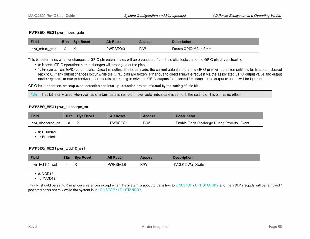
MAX32620 Rev C User Guide System Configuration and Management 4.2 Power Ecosystem and Operating Modes
PWRSEQ_REG1.pwr_mbus_gate
Field Bits Sys Reset Alt Reset Access Description
pwr_mbus_gate 2 X PWRSEQ:0 R/W Freeze GPIO MBus State
This bit determines whether changes to GPIO pin output states will be propagated from the digital logic out to the GPIO pin driver circuitry.• 0: Normal GPIO operation; output changes will propagate out to pins.• 1: Freeze current GPIO output state. Once this setting has been made, the current output state at the GPIO pins will be frozen until this bit has been cleared
back to 0. If any output changes occur while the GPIO pins are frozen, either due to direct firmware request via the associated GPIO output value and outputmode registers, or due to hardware peripherals attempting to drive the GPIO outputs for selected functions, these output changes will be ignored.
GPIO input operation, wakeup event detection and interrupt detection are not affected by the setting of this bit.
Note This bit is only used when pwr_auto_mbus_gate is set to 0. If pwr_auto_mbus gate is set to 1, the setting of this bit has no effect.
PWRSEQ_REG1.pwr_discharge_en
Field Bits Sys Reset Alt Reset Access Description
pwr_discharge_en 3 X PWRSEQ:0 R/W Enable Flash Discharge During Powerfail Event
• 0: Disabled• 1: Enabled
PWRSEQ_REG1.pwr_tvdd12_well
Field Bits Sys Reset Alt Reset Access Description
pwr_tvdd12_well 4 X PWRSEQ:0 R/W TVDD12 Well Switch
• 0: VDD12• 1: TVDD12
This bit should be set to 0 in all circumstances except when the system is about to transition to LP0:STOP / LP1:STANDBY and the VDD12 supply will be removed /powered down entirely while the system is in LP0:STOP / LP1:STANDBY.
Rev 2 Maxim Integrated Page 88

MAX32620 Rev C User Guide System Configuration and Management 4.2 Power Ecosystem and Operating Modes
PWRSEQ_REG1.pwr_sram_nwell_sw
Field Bits Sys Reset Access Description
pwr_sram_nwell_sw 5 0 R/W SRAM/Cache Well Switch
• 0: VDD12• 1: TVDD12
This bit should be set to 0 in all circumstances except when the system is about to transition to LP0:STOP / LP1:STANDBY and the VDD12 supply will be removed /powered down entirely while the system is in LP0:STOP / LP1:STANDBY.
PWRSEQ_REG1.pwr_auto_mbus_gate
Field Bits Sys Reset Access Description
pwr_auto_mbus_gate 6 0 R/W Automatically Set/Clear GPIO MBus Gate
Controls what method is used to freeze and resume GPIO MBus operation when going to sleep and waking up.• 0: Register based (pwr_mbus_gate). This setting should be used when the system is going into the LP0:STOP mode.• 1: Automatic (handled by hardware). This setting should be used when the system is going into the LP1:STANDBY mode.
Note In order for the GPIO output state to be maintained at the pins while the system is in LP0:STOP / LP1:STANDBY, the appropriate power supply orsupplies used by the GPIO (one or more of VDD18, VDDIO, and VDDIOH) must remain powered on.
PWRSEQ_REG1.pwr_svm_vddio_en_run
Field Bits Sys Reset Access Description
pwr_svm_vddio_en_run 8 1 R/W Enables SVM for VDDIO_SW during Run Mode
• 0: Disabled• 1: Enabled
Rev 2 Maxim Integrated Page 89

MAX32620 Rev C User Guide System Configuration and Management 4.2 Power Ecosystem and Operating Modes
PWRSEQ_REG1.pwr_svm_vddioh_en_run
Field Bits Sys Reset Access Description
pwr_svm_vddioh_en_run 10 0 R/W Enables SVM for VDDIOH_SW during Run Mode
• 0: Disabled• 1: Enabled
PWRSEQ_REG1.pwr_retreg_src_v12
Field Bits Sys Reset Access Description
pwr_retreg_src_v12 12 1 R/W Enables VDD12 Rail as Retention Power Supply
• 0: Disabled• 1: Enabled
Note CRITICAL - ONLY ENABLE ONE RAIL AT ONCE AS RETENTION SUPPLY.
PWRSEQ_REG1.pwr_retreg_src_vrtc
Field Bits Sys Reset Access Description
pwr_retreg_src_vrtc 13 0 R/W Enables VRTC Rail as Retention Power Supply
• 0: Disabled• 1: Enabled
Note CRITICAL - ONLY ENABLE ONE RAIL AT ONCE AS RETENTION SUPPLY.
Rev 2 Maxim Integrated Page 90

MAX32620 Rev C User Guide System Configuration and Management 4.2 Power Ecosystem and Operating Modes
PWRSEQ_REG1.pwr_retreg_src_v18
Field Bits Sys Reset Access Description
pwr_retreg_src_v18 14 0 R/W Enables VDD18 Rail as Retention Power Supply
• 0: Disabled• 1: Enabled
Note CRITICAL - ONLY ENABLE ONE RAIL AT ONCE AS RETENTION SUPPLY.
PWRSEQ_REG1.pwr_vddio_en_iso_por
Field Bits Sys Reset Access Description
pwr_vddio_en_iso_por 16 1 R/W Enable VDDIO Isolation POR
• 0: Disabled; all signals from VDDIO domain will never be isolated from other domains.• 1: Enabled
This bit should always be set to 1 (which is the default value) for proper system operation.
PWRSEQ_REG1.pwr_vddioh_en_iso_por
Field Bits Sys Reset Access Description
pwr_vddioh_en_iso_por 17 1 R/W Enable VDDIOH Isolation POR
• 0: Disabled; all signals from VDDIOH domain will never be isolated from other domains.• 1: Enabled
This bit should always be set to 1 (which is the default value) for proper system operation.
Rev 2 Maxim Integrated Page 91

MAX32620 Rev C User Guide System Configuration and Management 4.2 Power Ecosystem and Operating Modes
PWRSEQ_REG1.pwr_lp0_core_resume_en
Field Bits Sys Reset Access Description
pwr_lp0_core_resume_en 18 0 R/W Enable Core Resume to Toggle during LP0
• 0: Disabled• 1: Enabled
This bit should always be set to 0 (which is the default value) for proper system operation.
PWRSEQ_REG1.pwr_lp1_core_rstn_en
Field Bits Sys Reset Access Description
pwr_lp1_core_rstn_en 19 1 R/W Enable Core RSTN to Toggle during LP1
• 0: Disabled• 1: Enabled. This allows the core flip flops to be reset by RSTN during LP1 mode.
This bit should always be set to 1 (which is the default value) for proper system operation.
4.2.7.3 PWRSEQ_REG2
PWRSEQ_REG2.pwr_vdd12_hyst
Field Bits Sys Reset Alt Reset Access Description
pwr_vdd12_hyst 1:0 X PWRSEQ:1 R/W VDD12_SW Comparator Hysteresis Setting
• 0: 0 mV• 1: 12.5 mV (default)• 2: 25 mV• 3: 50 mV
This field should always be set to 1 (which is the default value) for proper system operation.
Rev 2 Maxim Integrated Page 92

MAX32620 Rev C User Guide System Configuration and Management 4.2 Power Ecosystem and Operating Modes
PWRSEQ_REG2.pwr_vdd18_hyst
Field Bits Sys Reset Alt Reset Access Description
pwr_vdd18_hyst 3:2 X PWRSEQ:1 R/W VDD18_SW Comparator Hysteresis Setting
• 0: 0 mV• 1: 12.5 mV (default)• 2: 25 mV• 3: 50 mV
This field should always be set to 1 (which is the default value) for proper system operation.
PWRSEQ_REG2.pwr_vrtc_hyst
Field Bits Sys Reset Alt Reset Access Description
pwr_vrtc_hyst 5:4 X PWRSEQ:1 R/W VRTC Comparator Hysteresis Setting
• 0: 0 mV• 1: 12.5 mV (default)• 2: 25 mV• 3: 50 mV
This field should always be set to 1 (which is the default value) for proper system operation.
PWRSEQ_REG2.pwr_vddb_hyst
Field Bits Sys Reset Alt Reset Access Description
pwr_vddb_hyst 7:6 X PWRSEQ:1 R/W VDDB Comparator Hysteresis Setting
• 0: 0 mV• 1: 12.5 mV (default)• 2: 25 mV• 3: 50 mV
This field should always be set to 1 (which is the default value) for proper system operation.
Rev 2 Maxim Integrated Page 93

MAX32620 Rev C User Guide System Configuration and Management 4.2 Power Ecosystem and Operating Modes
PWRSEQ_REG2.pwr_tvdd12_hyst
Field Bits Sys Reset Alt Reset Access Description
pwr_tvdd12_hyst 9:8 X PWRSEQ:1 R/W TVDD12 Comparator Hysteresis Setting
• 0: 0 mV• 1: 12.5 mV (default)• 2: 25 mV• 3: 50 mV
This field should always be set to 1 (which is the default value) for proper system operation.
PWRSEQ_REG2.pwr_vddio_hyst
Field Bits Sys Reset Access Description
pwr_vddio_hyst 11:10 1 R/W VDDIO Comparator Hysteresis Setting
• 0: 0 mV• 1: 12.5 mV (default)• 2: 25 mV• 3: 50 mV
This field should always be set to 1 (which is the default value) for proper system operation.
PWRSEQ_REG2.pwr_vddioh_hyst
Field Bits Sys Reset Access Description
pwr_vddioh_hyst 13:12 1 R/W VDDIOH Comparator Hysteresis Setting
• 0: 0 mV• 1: 12.5 mV (default)• 2: 25 mV• 3: 50 mV
This field should always be set to 1 (which is the default value) for proper system operation.
Rev 2 Maxim Integrated Page 94

MAX32620 Rev C User Guide System Configuration and Management 4.2 Power Ecosystem and Operating Modes
4.2.7.4 PWRSEQ_REG3
PWRSEQ_REG3.pwr_rosel
Field Bits Sys Reset Alt Reset Access Description
pwr_rosel 2:0 X PWRSEQ:5 R/W Relaxation Oscillator Stable Timeout for Wakeup
This timeout delay only applies when the device is transitioning back to Run mode from either LP0 or LP1. The timeout setting ensures that the currently selectedprimary system oscillator output has stabilized before code execution begins.
• 0: No delay (bypass)• 1: 4 clocks (of the currently selected primary system oscillator)• 2: 8 clocks• 3: 16 clocks• 4: 32 clocks• 5: 64 clocks (default, recommended setting)• 6: 128 clocks• 7: 256 clocks
This field should always be set to 5 (which is the default value) for proper system operation.
PWRSEQ_REG3.pwr_fltrrosel
Field Bits Sys Reset Alt Reset Access Description
pwr_fltrrosel 5:3 X PWRSEQ:3 R/W Power Supply Filter Timeout for Wakeup
This timeout delay only applies when the device is transitioning back to Run mode from either LP0 or LP1. The timeout setting ensures that the power supply hastime to stabilize before code execution begins.
• 0: No delay (bypass)• 1: 4 clocks (of the currently selected primary system oscillator)• 2: 8 clocks• 3: 16 clocks• 4: 32 clocks• 5: 64 clocks• 6: 128 clocks• 7: 256 clocks
Rev 2 Maxim Integrated Page 95

MAX32620 Rev C User Guide System Configuration and Management 4.2 Power Ecosystem and Operating Modes
PWRSEQ_REG3.pwr_svm_clk_mux
Field Bits Sys Reset Alt Reset Access Description
pwr_svm_clk_mux 7:6 X PWRSEQ:0 R/W SVM Clock Mux
• 0: Nanoring (default)• 1: RTC clock (for test purposes only)• 2: Relaxation oscillator (for test purposes only)• 3: External clock (for test purposes only)
This field is intended for internal test use only and should not be modified by user application firmware.
PWRSEQ_REG3.pwr_ro_clk_mux
Field Bits Sys Reset Alt Reset Access Description
pwr_ro_clk_mux 9:8 X PWRSEQ:0 R/W Relaxation Clock Mux
• 0: Relaxation oscillator (default)• 1: External clock (for test purposes only)• 2: Nanoring (for test purposes only)• 3: RTC clock (for test purposes only)
This field is intended for internal test use only and should not be modified by user application firmware.
Rev 2 Maxim Integrated Page 96

MAX32620 Rev C User Guide System Configuration and Management 4.2 Power Ecosystem and Operating Modes
PWRSEQ_REG3.pwr_failsel
Field Bits Sys Reset Alt Reset Access Description
pwr_failsel 12:10 X PWRSEQ:0 R/W Timeout before rebooting during PowerFail/BootFailevents.
These timeout values are based on the nanoring clock.• 0: No delay (default, this setting not recommended)• 1: 8ms (recommended setting)• 2: 16ms• 3: 32ms• 4: 64ms• 5: 128ms• 6: 256ms• 7: 512ms
For optimal system performance, this field should be set to 1 by application firmware following system startup. See System Configuration: Recommended Settings.
PWRSEQ_REG3.pwr_ro_div
Field Bits Sys Reset Access Description
pwr_ro_div 18:16 0 R/W Frequency Divider for 96MHz Relaxation Oscillator
This setting allows the output of the 96MHz relaxation Oscillator to be optionally divided down before it is used by other system functions.• 0: Divide by 1 - 96MHz output (default)• 1: Divide by 2 - 48MHz output• 2: Divide by 4 - 24MHz output• 3: Divide by 8 - 12MHz output• 4: Divide by 16 - 6MHz output
Rev 2 Maxim Integrated Page 97

MAX32620 Rev C User Guide System Configuration and Management 4.2 Power Ecosystem and Operating Modes
PWRSEQ_REG3.pwr_rc_div
Field Bits Sys Reset Access Description
pwr_rc_div 21:20 0 R/W Frequency Divider for 4MHz RC Oscillator
This setting allows the output of the 4MHz RC Oscillator to be optionally divided down before it is used by other system functions.• 0: Divide by 1 - 4MHz output (default)• 1: Divide by 2 - 2MHz output• 2: Divide by 4 - 1MHz output• 3: Divide by 8 - 0.5MHz output
4.2.7.5 PWRSEQ_REG4
PWRSEQ_REG4.pwr_tm_ps_2_gpio
Field Bits Sys Reset Alt Reset Access Description
pwr_tm_ps_2_gpio 0 X PWRSEQ:0 R/W Internal Use Only
This bit is intended for internal test use only and should not be modified by user application firmware.
PWRSEQ_REG4.pwr_tm_fast_timers
Field Bits Sys Reset Alt Reset Access Description
pwr_tm_fast_timers 1 X PWRSEQ:0 R/W Internal Use Only
This bit is intended for internal test use only and should not be modified by user application firmware.
PWRSEQ_REG4.pwr_usb_dis_comp
Field Bits Sys Reset Alt Reset Access Description
pwr_usb_dis_comp 3 X PWRSEQ:0 R/W Internal Use Only
This bit is intended for internal test use only and should not be modified by user application firmware.
Rev 2 Maxim Integrated Page 98

MAX32620 Rev C User Guide System Configuration and Management 4.2 Power Ecosystem and Operating Modes
PWRSEQ_REG4.pwr_ro_tstclk_en
Field Bits Sys Reset Alt Reset Access Description
pwr_ro_tstclk_en 4 X PWRSEQ:0 R/W Internal Use Only
This bit is intended for internal test use only and should not be modified by user application firmware.
PWRSEQ_REG4.pwr_nr_clk_gate_en
Field Bits Sys Reset Alt Reset Access Description
pwr_nr_clk_gate_en 5 X PWRSEQ:0 R/W Internal Use Only
This bit is intended for internal test use only and should not be modified by user application firmware.
PWRSEQ_REG4.pwr_ext_clk_in_en
Field Bits Sys Reset Alt Reset Access Description
pwr_ext_clk_in_en 6 X PWRSEQ:0 R/W Internal Use Only
This bit is intended for internal test use only and should not be modified by user application firmware.
PWRSEQ_REG4.pwr_pseq_32k_en
Field Bits Sys Reset Alt Reset Access Description
pwr_pseq_32k_en 7 X PWRSEQ:0 R/W Internal Use Only
This bit is intended for internal test use only and should not be modified by user application firmware.
Rev 2 Maxim Integrated Page 99

MAX32620 Rev C User Guide System Configuration and Management 4.2 Power Ecosystem and Operating Modes
PWRSEQ_REG4.pwr_rtc_mux
Field Bits Sys Reset Access Description
pwr_rtc_mux 8 0 R/W Internal Use Only
This bit is intended for internal test use only and should not be modified by user application firmware.
PWRSEQ_REG4.pwr_retreg_trim_lp1_en
Field Bits Sys Reset Access Description
pwr_retreg_trim_lp1_en 9 0 R/W Internal Use Only
This bit is intended for internal test use only and should not be modified by user application firmware.
PWRSEQ_REG4.pwr_usb_xvr_tst_en
Field Bits Sys Reset Access Description
pwr_usb_xvr_tst_en 10 0 R/W Internal Use Only
This bit is intended for internal test use only and should not be modified by user application firmware.
4.2.7.6 PWRSEQ_REG5
PWRSEQ_REG5.pwr_trim_svm_bg
Field Bits Sys Reset Alt Reset Access Description
pwr_trim_svm_bg 8:0 X PWRSEQ:0 R/W Power Manager Bandgap Trim Setting
This field must be initialized by firmware following initial powerup by copying from the TRIM_FOR_PWR_REG5 register to this register.
Rev 2 Maxim Integrated Page 100

MAX32620 Rev C User Guide System Configuration and Management 4.2 Power Ecosystem and Operating Modes
PWRSEQ_REG5.pwr_trim_bias
Field Bits Sys Reset Alt Reset Access Description
pwr_trim_bias 14:9 X PWRSEQ:0 R/W Power Manager Bias Current Trim Setting
This field must be initialized by firmware following initial powerup by copying from the TRIM_FOR_PWR_REG5 register to this register.
PWRSEQ_REG5.pwr_trim_retreg_5_0
Field Bits Sys Reset Alt Reset Access Description
pwr_trim_retreg_5_0 20:15 X PWRSEQ:0 R/W Retention Regulator Trim Setting (Bits 5:0)
This field must be initialized by firmware following initial powerup by copying from the TRIM_FOR_PWR_REG5 register to this register.
PWRSEQ_REG5.pwr_rtc_trim
Field Bits Sys Reset Alt Reset Access Description
pwr_rtc_trim 24:21 X PWRSEQ:0 R/W Real Time Clock Trim Setting
This field must be initialized by firmware following initial powerup by copying from the TRIM_FOR_PWR_REG5 register to this register.
PWRSEQ_REG5.pwr_trim_retreg_7_6
Field Bits Sys Reset Alt Reset Access Description
pwr_trim_retreg_7_6 26:25 X PWRSEQ:0 R/W Retention Regulator Trim Setting (Bits 7:6)
This field must be initialized by firmware following initial powerup by copying from the TRIM_FOR_PWR_REG5 register to this register.
Rev 2 Maxim Integrated Page 101

MAX32620 Rev C User Guide System Configuration and Management 4.2 Power Ecosystem and Operating Modes
4.2.7.7 PWRSEQ_REG6
PWRSEQ_REG6.pwr_trim_usb_bias
Field Bits Sys Reset Alt Reset Access Description
pwr_trim_usb_bias 2:0 X PWRSEQ:0 R/W USB Bias Current Trim Setting
This field must be initialized by firmware following initial powerup by copying from the TRIM_FOR_PWR_REG6 register to this register.
PWRSEQ_REG6.pwr_trim_usb_pm_res
Field Bits Sys Reset Alt Reset Access Description
pwr_trim_usb_pm_res 6:3 X PWRSEQ:0 R/W USB Data Plus Slew Rate Trim Setting
This field must be initialized by firmware following initial powerup by copying from the TRIM_FOR_PWR_REG6 register to this register.
PWRSEQ_REG6.pwr_trim_usb_dm_res
Field Bits Sys Reset Alt Reset Access Description
pwr_trim_usb_dm_res 10:7 X PWRSEQ:0 R/W USB Data Minus Slew Rate Trim Setting
This field must be initialized by firmware following initial powerup by copying from the TRIM_FOR_PWR_REG6 register to this register.
PWRSEQ_REG6.pwr_trim_osc_vref
Field Bits Sys Reset Alt Reset Access Description
pwr_trim_osc_vref 19:11 X PWRSEQ:17Ch R/W Relaxation Oscillator Trim Setting
This field must be initialized by firmware following initial powerup by copying from the TRIM_FOR_PWR_REG6 register to this register.
Rev 2 Maxim Integrated Page 102

MAX32620 Rev C User Guide System Configuration and Management 4.2 Power Ecosystem and Operating Modes
PWRSEQ_REG6.pwr_trim_crypto_osc
Field Bits Sys Reset Alt Reset Access Description
pwr_trim_crypto_osc 28:20 X PWRSEQ:0 R/W Crypto Oscillator Trim Setting
This field must be initialized by firmware following initial powerup by copying from the TRIM_FOR_PWR_REG6 register to this register.
4.2.7.8 PWRSEQ_REG7
PWRSEQ_REG7.pwr_flash_pd_lookahead
Field Bits Sys Reset Access Description
pwr_flash_pd_lookahead 0 0 R/O Flash Powerdown Lookahead Flag
When this flag returns 1, the flash is about to be powered down in preparation for entry to LP0 or LP1 mode.
PWRSEQ_REG7.pwr_trim_rc
Field Bits Sys Reset Alt Reset Access Description
pwr_trim_rc 31:16 X PWRSEQ:0 R/W Trim Setting for 4MHz Internal RC Oscillator
This field must be initialized by firmware following initial powerup by copying from the TRIM_FOR_PWR_REG7 register to this register.
4.2.7.9 PWRSEQ_FLAGS
PWRSEQ_FLAGS.pwr_first_boot
Field Bits Sys Reset Access Description
pwr_first_boot 0 s R/O Initial Boot Event Detected Flag
Rev 2 Maxim Integrated Page 103

MAX32620 Rev C User Guide System Configuration and Management 4.2 Power Ecosystem and Operating Modes
PWRSEQ_FLAGS.pwr_sys_reboot
Field Bits Sys Reset Access Description
pwr_sys_reboot 1 s R/O Firmware Reset Event Detected Flag
PWRSEQ_FLAGS.pwr_power_fail
Field Bits Sys Reset Access Description
pwr_power_fail 2 s W1C Power Fail Event Detected Flag
Write 1 to clear event detected flag.
PWRSEQ_FLAGS.pwr_boot_fail
Field Bits Sys Reset Access Description
pwr_boot_fail 3 s W1C Boot Fail Event Detected Flag
Write 1 to clear event detected flag.
PWRSEQ_FLAGS.pwr_flash_discharge
Field Bits Sys Reset Access Description
pwr_flash_discharge 4 s W1C Flash Discharged During Powerfail Event DetectedFlag
Write 1 to clear event detected flag.
Rev 2 Maxim Integrated Page 104

MAX32620 Rev C User Guide System Configuration and Management 4.2 Power Ecosystem and Operating Modes
PWRSEQ_FLAGS.pwr_iowakeup
Field Bits Sys Reset Access Description
pwr_iowakeup 5 s W1C GPIO Wakeup Event Detected Flag
Write 1 to clear event detected flag.
PWRSEQ_FLAGS.pwr_vdd12_rst_bad
Field Bits Sys Reset Access Description
pwr_vdd12_rst_bad 6 s W1C VDD12_SW Comparator Tripped Event Detected Flag
Write 1 to clear event detected flag.
PWRSEQ_FLAGS.pwr_vdd18_rst_bad
Field Bits Sys Reset Access Description
pwr_vdd18_rst_bad 7 s W1C VDD18_SW Comparator Tripped Event Detected Flag
Write 1 to clear event detected flag.
PWRSEQ_FLAGS.pwr_vrtc_rst_bad
Field Bits Sys Reset Access Description
pwr_vrtc_rst_bad 8 s W1C VRTC Comparator Tripped Event Detected Flag
Write 1 to clear event detected flag.
Rev 2 Maxim Integrated Page 105

MAX32620 Rev C User Guide System Configuration and Management 4.2 Power Ecosystem and Operating Modes
PWRSEQ_FLAGS.pwr_vddb_rst_bad
Field Bits Sys Reset Access Description
pwr_vddb_rst_bad 9 s W1C VDDB Comparator Tripped Event Detected Flag
Write 1 to clear event detected flag.
PWRSEQ_FLAGS.pwr_tvdd12_rst_bad
Field Bits Sys Reset Access Description
pwr_tvdd12_rst_bad 10 s W1C TVDD12 Comparator Tripped Event Detected Flag
Write 1 to clear event detected flag.
PWRSEQ_FLAGS.pwr_por18z_fail_latch
Field Bits Sys Reset Access Description
pwr_por18z_fail_latch 11 s W1C POR18 and POR18_bg have been tripped
Write 1 to clear event detected flag.
PWRSEQ_FLAGS.rtc_cmpr0
Field Bits Sys Reset Access Description
rtc_cmpr0 12 s R/O RTC Comparator 0 Match Event Detected Flag
Write 1 to clear event detected flag.
Rev 2 Maxim Integrated Page 106

MAX32620 Rev C User Guide System Configuration and Management 4.2 Power Ecosystem and Operating Modes
PWRSEQ_FLAGS.rtc_cmpr1
Field Bits Sys Reset Access Description
rtc_cmpr1 13 s R/O RTC Comparator 1 Match Event Detected Flag
Write 1 to clear event detected flag.
PWRSEQ_FLAGS.rtc_prescale_cmp
Field Bits Sys Reset Access Description
rtc_prescale_cmp 14 s R/O RTC Prescale Comparator Match Event Detected Flag
Write 1 to clear event detected flag.
PWRSEQ_FLAGS.rtc_rollover
Field Bits Sys Reset Access Description
rtc_rollover 15 s R/O RTC Rollover Event Detected Flag
Write 1 to clear event detected flag.
PWRSEQ_FLAGS.pwr_usb_plug_wakeup
Field Bits Sys Reset Access Description
pwr_usb_plug_wakeup 16 s W1C USB Power Connect Wakeup Event Detected Flag
Write 1 to clear event detected flag.
Rev 2 Maxim Integrated Page 107

MAX32620 Rev C User Guide System Configuration and Management 4.2 Power Ecosystem and Operating Modes
PWRSEQ_FLAGS.pwr_usb_remove_wakeup
Field Bits Sys Reset Access Description
pwr_usb_remove_wakeup 17 s W1C USB Power Remove Wakeup Event Detected Flag
Write 1 to clear event detected flag.
PWRSEQ_FLAGS.pwr_tvdd12_bad
Field Bits Sys Reset Access Description
pwr_tvdd12_bad 18 s W1C Retention Regulator POR Tripped Event Detected Flag
Write 1 to clear event detected flag.
PWRSEQ_FLAGS.pwr_vddio_rst_bad
Field Bits Sys Reset Access Description
pwr_vddio_rst_bad 19 s W1C VDDIO Comparator Tripped
Write 1 to clear event detected flag.
PWRSEQ_FLAGS.pwr_vddioh_rst_bad
Field Bits Sys Reset Access Description
pwr_vddioh_rst_bad 20 s W1C VDDIOH Comparator Tripped
Write 1 to clear event detected flag.
Rev 2 Maxim Integrated Page 108

MAX32620 Rev C User Guide System Configuration and Management 4.2 Power Ecosystem and Operating Modes
PWRSEQ_FLAGS.pwr_isoz_vddio_fail
Field Bits Sys Reset Access Description
pwr_isoz_vddio_fail 21 s W1C VDDIO Isolation POR Tripped
Write 1 to clear event detected flag.
PWRSEQ_FLAGS.pwr_isoz_vddioh_fail
Field Bits Sys Reset Access Description
pwr_isoz_vddioh_fail 22 s W1C VDDIOH Isolation POR Tripped
Write 1 to clear event detected flag.
PWRSEQ_FLAGS.pwr_nanoring_wakeup_flag
Field Bits Sys Reset Access Description
pwr_nanoring_wakeup_flag 23 s W1C Wakeup Triggered by WDT2 Flag
Write 1 to clear event detected flag.
PWRSEQ_FLAGS.pwr_watchdog_rstn_flag
Field Bits Sys Reset Access Description
pwr_watchdog_rstn_flag 24 s W1C Power Sequencer Reset Triggered by WDT2 Flag
Write 1 to clear event detected flag.
Rev 2 Maxim Integrated Page 109

MAX32620 Rev C User Guide System Configuration and Management 4.2 Power Ecosystem and Operating Modes
4.2.7.10 PWRSEQ_MSK_FLAGS
PWRSEQ_MSK_FLAGS.pwr_sys_reboot
Field Bits Sys Reset Alt Reset Access Description
pwr_sys_reboot 1 X PWRSEQ:1 R/W Mask for system reboot detect
• 0: No effect.• 1: If a watchdog is asserting a system reboot output, this will cause the device to wake up from LP0.
PWRSEQ_MSK_FLAGS.pwr_power_fail
Field Bits Sys Reset Alt Reset Access Description
pwr_power_fail 2 X PWRSEQ:1 R/W Mask for previous power fail detect
• 0: Normal operation.• 1: The power sequencer will not shut down due to a power fail event.
PWRSEQ_MSK_FLAGS.pwr_boot_fail
Field Bits Sys Reset Alt Reset Access Description
pwr_boot_fail 3 X PWRSEQ:1 R/W Mask for previous boot fail detect
• 0: Normal operation.• 1: The power sequencer will not restart the boot/resume sequence due to a boot failure event.
PWRSEQ_MSK_FLAGS.pwr_flash_discharge
Field Bits Sys Reset Alt Reset Access Description
pwr_flash_discharge 4 X PWRSEQ:1 R/W Mask for flash discharge event
• 0: Normal operation.• 1: The power sequencer will not safely discharge flash in the event of a power failure.
Rev 2 Maxim Integrated Page 110

MAX32620 Rev C User Guide System Configuration and Management 4.2 Power Ecosystem and Operating Modes
PWRSEQ_MSK_FLAGS.pwr_iowakeup
Field Bits Sys Reset Alt Reset Access Description
pwr_iowakeup 5 X PWRSEQ:1 R/W Mask for GPIO wakeup event detect
• 0: GPIO pins cannot be used for wakeup detection. Also, in this mode, an active low external reset on SRSTn will not wake the device up from LP1 or LP0.• 1: GPIO pins can be used for wakeup detection in LP1/LP0 (note that wakeup detection must be enabled individually for each GPIO pin that will be used in
this manner). Also, wakeup detection will be enabled on the SRSTn pin for LP1/LP0.
PWRSEQ_MSK_FLAGS.pwr_vdd12_rst_bad
Field Bits Sys Reset Alt Reset Access Description
pwr_vdd12_rst_bad 6 X PWRSEQ:1 R/W Mask for VDD12 rst event
• 0: Normal operation.• 1: The power sequencer will not shut down due to a VDD12 rst event.
PWRSEQ_MSK_FLAGS.pwr_vdd18_rst_bad
Field Bits Sys Reset Alt Reset Access Description
pwr_vdd18_rst_bad 7 X PWRSEQ:1 R/W Mask for VDD18 rst event
• 0: Normal operation.• 1: The power sequencer will not shut down due to a VDD18 rst event.
PWRSEQ_MSK_FLAGS.pwr_vrtc_rst_bad
Field Bits Sys Reset Alt Reset Access Description
pwr_vrtc_rst_bad 8 X PWRSEQ:1 R/W Mask for VRTC rst event
• 0: Normal operation.• 1: The power sequencer will not shut down due to a VRTC rst event.
Rev 2 Maxim Integrated Page 111

MAX32620 Rev C User Guide System Configuration and Management 4.2 Power Ecosystem and Operating Modes
PWRSEQ_MSK_FLAGS.pwr_vddb_rst_bad
Field Bits Sys Reset Alt Reset Access Description
pwr_vddb_rst_bad 9 X PWRSEQ:1 R/W Mask for VDDB rst event
• 0: Normal operation.• 1: The power sequencer will not shut down due to a VDDB rst event.
PWRSEQ_MSK_FLAGS.pwr_tvdd12_rst_bad
Field Bits Sys Reset Alt Reset Access Description
pwr_tvdd12_rst_bad 10 X PWRSEQ:1 R/W Mask for TVDD12 rst event
• 0: Normal operation.• 1: The power sequencer will not shut down due to a TVDD12 rst event.
PWRSEQ_MSK_FLAGS.pwr_por18z_fail_latch
Field Bits Sys Reset Alt Reset Access Description
pwr_por18z_fail_latch 11 X PWRSEQ:1 R/W Mask for POR18 powerfail event
• 0: Normal operation.• 1: The power sequencer will not latch any POR18 powerfail event.
PWRSEQ_MSK_FLAGS.rtc_cmpr0
Field Bits Sys Reset Alt Reset Access Description
rtc_cmpr0 12 X PWRSEQ:1 R/W Mask for RTC compare 0 event
If (PWRSEQ_PWR_MISC.invert_4_mask_bits == 0), this mask bit will operate with inverted sense compared to the other non-RTC mask bits, as follows.• 0: Event can be detected and used as a wakeup source• 1: Event is masked
If (PWRSEQ_PWR_MISC.invert_4_mask_bits == 1), this mask bit will operate similarly to the other non-RTC mask bits, as follows.• 0: Event is masked.• 1: Event can be detected and used as a wakeup source.
Rev 2 Maxim Integrated Page 112

MAX32620 Rev C User Guide System Configuration and Management 4.2 Power Ecosystem and Operating Modes
PWRSEQ_MSK_FLAGS.rtc_cmpr1
Field Bits Sys Reset Alt Reset Access Description
rtc_cmpr1 13 X PWRSEQ:1 R/W Mask for RTC compare 1 event
If (PWRSEQ_PWR_MISC.invert_4_mask_bits == 0), this mask bit will operate with inverted sense compared to the other non-RTC mask bits, as follows.• 0: Event can be detected and used as a wakeup source• 1: Event is masked
If (PWRSEQ_PWR_MISC.invert_4_mask_bits == 1), this mask bit will operate similarly to the other non-RTC mask bits, as follows.• 0: Event is masked.• 1: Event can be detected and used as a wakeup source.
PWRSEQ_MSK_FLAGS.rtc_prescale_cmp
Field Bits Sys Reset Alt Reset Access Description
rtc_prescale_cmp 14 X PWRSEQ:1 R/W Mask for RTC prescale compare event
If (PWRSEQ_PWR_MISC.invert_4_mask_bits == 0), this mask bit will operate with inverted sense compared to the other non-RTC mask bits, as follows.• 0: Event can be detected and used as a wakeup source• 1: Event is masked
If (PWRSEQ_PWR_MISC.invert_4_mask_bits == 1), this mask bit will operate similarly to the other non-RTC mask bits, as follows.• 0: Event is masked.• 1: Event can be detected and used as a wakeup source.
Rev 2 Maxim Integrated Page 113

MAX32620 Rev C User Guide System Configuration and Management 4.2 Power Ecosystem and Operating Modes
PWRSEQ_MSK_FLAGS.rtc_rollover
Field Bits Sys Reset Alt Reset Access Description
rtc_rollover 15 X PWRSEQ:1 R/W Mask for RTC rollover event
If (PWRSEQ_PWR_MISC.invert_4_mask_bits == 0), this mask bit will operate with inverted sense compared to the other non-RTC mask bits, as follows.• 0: Event can be detected and used as a wakeup source• 1: Event is masked
If (PWRSEQ_PWR_MISC.invert_4_mask_bits == 1), this mask bit will operate similarly to the other non-RTC mask bits, as follows.• 0: Event is masked.• 1: Event can be detected and used as a wakeup source.
PWRSEQ_MSK_FLAGS.pwr_usb_plug_wakeup
Field Bits Sys Reset Alt Reset Access Description
pwr_usb_plug_wakeup 16 X PWRSEQ:1 R/W Mask for USB plug connect event
• 0: Event is masked• 1: Event can be detected and used as a wakeup source
PWRSEQ_MSK_FLAGS.pwr_usb_remove_wakeup
Field Bits Sys Reset Alt Reset Access Description
pwr_usb_remove_wakeup 17 X PWRSEQ:1 R/W Mask for USB plug disconnect event
• 0: Event is masked• 1: Event can be detected and used as a wakeup source
Rev 2 Maxim Integrated Page 114

MAX32620 Rev C User Guide System Configuration and Management 4.2 Power Ecosystem and Operating Modes
PWRSEQ_MSK_FLAGS.pwr_tvdd12_bad
Field Bits Sys Reset Alt Reset Access Description
pwr_tvdd12_bad 18 X PWRSEQ:1 R/W Mask for TVDD12 power fail event
• 0: Normal operation.• 1: The power sequencer will not shut down due to a TVDD12 power fail event (applies during LP1 only).
PWRSEQ_MSK_FLAGS.pwr_vddio_rst_bad
Field Bits Sys Reset Access Description
pwr_vddio_rst_bad 19 1 R/W Mask for VDDIO Comparator
• 0: Event is masked• 1: Event can be detected and used as a wakeup source
PWRSEQ_MSK_FLAGS.pwr_vddioh_rst_bad
Field Bits Sys Reset Access Description
pwr_vddioh_rst_bad 20 0 R/W Mask for VDDIOH Comparator
• 0: Event is masked• 1: Event can be detected and used as a wakeup source
PWRSEQ_MSK_FLAGS.pwr_isoz_vddio_fail
Field Bits Sys Reset Access Description
pwr_isoz_vddio_fail 21 1 R/W Mask for VDDIO Isolation POR
• 0: Event is masked• 1: Event can be detected and used as a wakeup source
Rev 2 Maxim Integrated Page 115

MAX32620 Rev C User Guide System Configuration and Management 4.2 Power Ecosystem and Operating Modes
PWRSEQ_MSK_FLAGS.pwr_isoz_vddioh_fail
Field Bits Sys Reset Access Description
pwr_isoz_vddioh_fail 22 0 R/W Mask for VDDIOH Isolation POR
• 0: Event is masked• 1: Event can be detected and used as a wakeup source
PWRSEQ_MSK_FLAGS.pwr_nanoring_wakeup_flag
Field Bits Sys Reset Access Description
pwr_nanoring_wakeup_flag 23 1 R/W Mask for WDT2 Wakeup Event
• 0: Event is masked• 1: Event can be detected and used as a wakeup source
PWRSEQ_MSK_FLAGS.pwr_watchdog_rstn_flag
Field Bits Sys Reset Access Description
pwr_watchdog_rstn_flag 24 0 R/W Mask for WDT2 PWRSEQ Reset (Internal RSTN)Event
• 0: Event is masked• 1: Event can be detected and used as a wakeup source
4.2.7.11 PWRSEQ_WR_PROTECT
PWRSEQ_WR_PROTECT.bypass_seq
Field Bits Sys Reset Access Description
bypass_seq 7:0 0 W/O Write Protect Bypass Sequence Write
This field is used to set the Write Protect Bypass bit to 1. To set the Write Protect Bypass bit, write the following sequence of values to this field: 0x88, 0xDD, 0x22.
The Write Protect Bypass bit will automatically clear when any value out of the sequence is written to this field.
Rev 2 Maxim Integrated Page 116

MAX32620 Rev C User Guide System Configuration and Management 4.2 Power Ecosystem and Operating Modes
PWRSEQ_WR_PROTECT.rtc_seq
Field Bits Sys Reset Access Description
rtc_seq 15:8 0 W/O Write Protect RTC Sequence Write
This field is used to change the value of the Write Protect from RTC bit. To toggle the Write Protect from RTC value, write the following sequence of values to thisfield: 0x44, 0xBB, 0x66.
PWRSEQ_WR_PROTECT.rtc
Field Bits Sys Reset Access Description
rtc 28 0 R/O Write Protect from RTC
The value of this bit can be toggled by writing the proper sequence of values to Write Protect RTC Sequence Write.
PWRSEQ_WR_PROTECT.info
Field Bits Sys Reset Access Description
info 29 0 R/O Write Protect from Info Block
The value of this bit is determined by a setting loaded into the info block. This bit cannot be modified by application firmware.
PWRSEQ_WR_PROTECT.bypass
Field Bits Sys Reset Access Description
bypass 30 0 R/O Write Protect Bypass
When this field is set to 1, the Critical Setting Write Protect is bypassed.
Rev 2 Maxim Integrated Page 117

MAX32620 Rev C User Guide System Configuration and Management 4.2 Power Ecosystem and Operating Modes
PWRSEQ_WR_PROTECT.wp
Field Bits Sys Reset Access Description
wp 31 0 R/O Critical Setting Write Protect
This read-only bit is a logical OR of the values of the Write Protect from RTC and Write Protect from Info Block bits.• 0: No effect.• 1: Critical fields/registers in the RTC and PWRSEQ register blocks will be protected against modification UNLESS the Write Protect Bypass bit is set to 1.
4.2.7.12 PWRSEQ_RETN_CTRL0
PWRSEQ_RETN_CTRL0.retn_ctrl_en
Field Bits Sys Reset Alt Reset Access Description
retn_ctrl_en 0 X PWRSEQ:0 R/W Retention Controller Enable
This bit controls the top-level enable/disable mode for the retention controller.• 0: Disabled.• 1: Enabled.
PWRSEQ_RETN_CTRL0.rc_rel_ccg_early
Field Bits Sys Reset Alt Reset Access Description
rc_rel_ccg_early 1 X PWRSEQ:0 R/W Early Core Clock Gate Release
• 0: Normal behavior.• 1: Allows the retention controller to release the core clock gate early, before the TWake period has expired.
PWRSEQ_RETN_CTRL0.rc_use_flc_twk
Field Bits Sys Reset Alt Reset Access Description
rc_use_flc_twk 2 X PWRSEQ:1 R/W Enable Flash Controller TWake Timer
• 0: Flash controller TWake is ignored.• 1: Allow the flash controller to implement its own TWake timeout.
Rev 2 Maxim Integrated Page 118

MAX32620 Rev C User Guide System Configuration and Management 4.2 Power Ecosystem and Operating Modes
PWRSEQ_RETN_CTRL0.rc_poll_flash
Field Bits Sys Reset Alt Reset Access Description
rc_poll_flash 3 X PWRSEQ:0 R/W Enable Automatic Flash Polling for Wakeup
• 0: Normal behavior.• 1: Allow automatic polling of the flash memory to determine when the flash is awake and ready for use by the application.
PWRSEQ_RETN_CTRL0.restore_override
Field Bits Sys Reset Alt Reset Access Description
restore_override 4 X PWRSEQ:0 R/W Restore Override (Reserved).
Reserved. For proper retention controller operation, this bit should always be set to 0.
4.2.7.13 PWRSEQ_RETN_CTRL1
PWRSEQ_RETN_CTRL1.rc_twk
Field Bits Sys Reset Alt Reset Access Description
rc_twk 3:0 X PWRSEQ:0xB R/W Retention Controller TWake Cycle Count
The number of micro seconds before the twk (flash timer wakeup period) stage of retention controller is complete, thus enabling the flash controller to take over(which may or may not implement its own twk circuit).
PWRSEQ_RETN_CTRL1.sram_fms
Field Bits Sys Reset Alt Reset Access Description
sram_fms 7:4 X PWRSEQ:0xC R/W SRAM Margin Setting (Reserved).
Reserved. For proper operation, this field should be left at its default value.
Rev 2 Maxim Integrated Page 119

MAX32620 Rev C User Guide System Configuration and Management 4.2 Power Ecosystem and Operating Modes
4.2.7.14 PWRSEQ_PWR_MISC
PWRSEQ_PWR_MISC.invert_4_mask_bits
Field Bits Sys Reset Alt Reset Access Description
invert_4_mask_bits 0 X PWRSEQ:0 R/W Invert Sense of Power Mask Flags for RTC
This bit controls the active sense (but not the default value) of the four power mask bits in PWRSEQ_MSK_FLAGS bits 12, 13, 14 and 15 as follows.• 0: Backwards compatible behavior for legacy firmware. Each of these four mask bits will mask the related RTC wakeup source when set to 1, and enable use
of the RTC wakeup source when set to 0. This is backwards from the other mask bits defined in the register.• 1: These four bits will mask the related RTC wakeup source when set to 0, and will allow use of the RTC wakeup source when set to 1. (This is the
recommended setting, see System Configuration: Recommended Settings).
4.2.7.15 PWRSEQ_RTC_CTRL2
PWRSEQ_RTC_CTRL2.timer_async_rd
Field Bits Sys Reset Alt Reset Access Description
timer_async_rd 0 X PWRSEQ:0 R/W TBD
PWRSEQ_RTC_CTRL2.timer_async_wr
Field Bits Sys Reset Alt Reset Access Description
timer_async_wr 1 X PWRSEQ:0 R/W TBD
PWRSEQ_RTC_CTRL2.timer_auto_update
Field Bits Sys Reset Alt Reset Access Description
timer_auto_update 2 X PWRSEQ:0 R/W TBD
Rev 2 Maxim Integrated Page 120

MAX32620 Rev C User Guide System Configuration and Management 4.2 Power Ecosystem and Operating Modes
PWRSEQ_RTC_CTRL2.ssb_performance
Field Bits Sys Reset Alt Reset Access Description
ssb_performance 3 X PWRSEQ:0 R/W TBD
PWRSEQ_RTC_CTRL2.cfg_lock
Field Bits Sys Reset Alt Reset Access Description
cfg_lock 31:24 X PWRSEQ:0 R/W TBD
Rev 2 Maxim Integrated Page 121

MAX32620 Rev C User Guide System Configuration and Management 4.2 Power Ecosystem and Operating Modes
4.2.8 Registers (PWRMAN)
Address Register Access Description Reset By
0x4000_0800 PWRMAN_PWR_RST_CTRL ∗∗∗ Power Reset Control and Status Sys
0x4000_0804 PWRMAN_INTFL W1C Interrupt Flags Sys
0x4000_0808 PWRMAN_INTEN R/W Interrupt Enable/Disable Controls Sys
0x4000_080C PWRMAN_SVM_EVENTS R/O Supply Voltage Monitor Reset Status Sys
0x4000_0810 PWRMAN_WUD_CTRL R/W Wake-Up Detect Control Sys
0x4000_0814 PWRMAN_WUD_PULSE0 W/O WUD Pulse To Mode Bit 0 Sys
0x4000_0818 PWRMAN_WUD_PULSE1 W/O WUD Pulse To Mode Bit 1 Sys
0x4000_081C PWRMAN_WUD_SEEN0 R/O Wake-up Detect Status for P0/P1/P2/P3 Sys
0x4000_0820 PWRMAN_WUD_SEEN1 R/O Wake-up Detect Status for P4/P5/P6 Sys
0x4000_0830 PWRMAN_PT_REGMAP_CTRL R/W PT Register Mapping Control Sys
0x4000_0838 PWRMAN_DIE_TYPE R/O Die Type ID Register Sys
0x4000_083C PWRMAN_BASE_PART_NUM R/O Base Part Number
0x4000_0840 PWRMAN_MASK_ID0 R/O Mask ID Register 0
0x4000_0844 PWRMAN_MASK_ID1 ∗∗∗ Mask ID Register 1 Sys
0x4000_0848 PWRMAN_PERIPHERAL_RESET R/W Peripheral Reset Control Register Sys
Rev 2 Maxim Integrated Page 122

MAX32620 Rev C User Guide System Configuration and Management 4.2 Power Ecosystem and Operating Modes
4.2.8.1 PWRMAN_PWR_RST_CTRL
PWRMAN_PWR_RST_CTRL.afe_powered
Field Bits Sys Reset Access Description
afe_powered 2 0 R/W Reserved
This bit is reserved and should not be modified by application firmware.
PWRMAN_PWR_RST_CTRL.io_active
Field Bits Sys Reset Access Description
io_active 3 1 R/W I/O Active
• 0: Puts all I/O (GPIO-only) pins in the lowest power state.• 1: All I/O pins are powered on normally.
PWRMAN_PWR_RST_CTRL.usb_powered
Field Bits Sys Reset Access Description
usb_powered 4 0 R/W Power Up USB Block
• 0: Digital portion of USB block is powered down. (default)• 1: Digital portion of USB block is powered up.
This bit must be set to 1 in order to use the USB peripheral. Note that for the USB peripheral to be fully powered, this bit must be set to 1, and the VDDB supply (whichpowers the USB PHY) must also be powered as defined in the device datasheet.
PWRMAN_PWR_RST_CTRL.pullups_enabled
Field Bits Sys Reset Access Description
pullups_enabled 5 1 R/W Enable Dedicated Pin Internal Pullups
• 0: Internal pullup resistors on the dedicated pins are disabled.• 1: Internal pullups on the dedicated pins are enabled (default).
The pins that this control bit applies to are as follows:
Rev 2 Maxim Integrated Page 123

MAX32620 Rev C User Guide System Configuration and Management 4.2 Power Ecosystem and Operating Modes
• TCK/SWCLK, TMS/SWDIO, TDI: 25kΩ pullup to VDDIO
• SRSTN: 25kΩ pullup to VDDIO
• RSTN: 25kΩ pullup to VRTC
Note that if any of these pins are left disconnected (not driven by an external signal), then the dedicated pin internal pullups must be left enabled for proper systemoperation.
PWRMAN_PWR_RST_CTRL.firmware_reset
Field Bits Sys Reset Access Description
firmware_reset 8 0 W1T Trigger Firmware Initiated Reset From PwrMan
Initiates a system reset when set to 1. This bit is self-clearing.
PWRMAN_PWR_RST_CTRL.arm_lockup_reset
Field Bits Sys Reset Access Description
arm_lockup_reset 9 0 R/W Enable System Reset Triggered by ARM Core Lockup
If this bit is set to 1, a system reset will be automatically triggered when the ARM core asserts its lockup state output signal.
PWRMAN_PWR_RST_CTRL.tamper_detect
Field Bits Sys Reset Access Description
tamper_detect 16 refer to desc R/O Reserved
Not applicable; the value of this bit should be disregarded.
PWRMAN_PWR_RST_CTRL.arm_lockup
Field Bits Sys Reset Access Description
arm_lockup 17 refer to desc R/O Last Reset Caused By ARM Core Lockup
Rev 2 Maxim Integrated Page 124

MAX32620 Rev C User Guide System Configuration and Management 4.2 Power Ecosystem and Operating Modes
PWRMAN_PWR_RST_CTRL.fw_command_arm
Field Bits Sys Reset Access Description
fw_command_arm 18 refer to desc R/O Last Reset Caused By Firmware Initiated Reset FromARM Core
PWRMAN_PWR_RST_CTRL.watchdog_timeout
Field Bits Sys Reset Access Description
watchdog_timeout 19 refer to desc R/O Last Reset Caused By Watchdog Timeout
PWRMAN_PWR_RST_CTRL.fw_command_sysman
Field Bits Sys Reset Access Description
fw_command_sysman 20 refer to desc R/O Last Reset Caused By Firmware Initated Reset FromPwrMan
PWRMAN_PWR_RST_CTRL.srstn_assertion
Field Bits Sys Reset Access Description
srstn_assertion 21 refer to desc R/O Last Reset Caused By Assertion of SRSTn
PWRMAN_PWR_RST_CTRL.por
Field Bits Sys Reset Access Description
por 22 refer to desc R/O Last Reset Caused By Power On Reset (POR)
Rev 2 Maxim Integrated Page 125

MAX32620 Rev C User Guide System Configuration and Management 4.2 Power Ecosystem and Operating Modes
PWRMAN_PWR_RST_CTRL.low_power_mode
Field Bits Sys Reset Access Description
low_power_mode 31 0 R/W Enable Power Manager Dynamic Clock Gating
1: Enables dynamic clock gating for pwrman functions.
4.2.8.2 PWRMAN_INTFL
PWRMAN_INTFL.v1_2_reset
Field Bits Sys Reset Access Description
v1_2_reset 0 0 W1C 1.2V Supply Reset Interrupt Flag
• 0: No reset condition has occurred on the specified power supply.• 1: The power supply has dropped below the minimum allowed voltage level.
This flag is set to 1 by hardware when the associated power supply drops below the minimum allowed voltage level. Hardware does not auto-clear this flag, so evenif the power supply subsequently rises above the minimum level, this flag will not be cleared by hardware. Firmware must clear this flag after handling the interrupt.
Write 1 to clear.
PWRMAN_INTFL.v1_8_reset
Field Bits Sys Reset Access Description
v1_8_reset 1 0 W1C 1.8V Supply Reset Interrupt Flag
• 0: No reset condition has occurred on the specified power supply.• 1: The power supply has dropped below the minimum allowed voltage level.
This flag is set to 1 by hardware when the associated power supply drops below the minimum allowed voltage level. Hardware does not auto-clear this flag, so evenif the power supply subsequently rises above the minimum level, this flag will not be cleared by hardware. Firmware must clear this flag after handling the interrupt.
Write 1 to clear.
Rev 2 Maxim Integrated Page 126

MAX32620 Rev C User Guide System Configuration and Management 4.2 Power Ecosystem and Operating Modes
PWRMAN_INTFL.rtc_reset
Field Bits Sys Reset Access Description
rtc_reset 2 0 W1C RTC Supply Reset Interrupt Flag
• 0: No reset condition has occurred on the specified power supply.• 1: The power supply has dropped below the minimum allowed voltage level.
This flag is set to 1 by hardware when the associated power supply drops below the minimum allowed voltage level. Hardware does not auto-clear this flag, so evenif the power supply subsequently rises above the minimum level, this flag will not be cleared by hardware. Firmware must clear this flag after handling the interrupt.
Write 1 to clear.
PWRMAN_INTFL.tvdd12_reset
Field Bits Sys Reset Access Description
tvdd12_reset 3 0 W1C TVDD12 Supply Reset Interrupt Flag
• 0: No reset condition has occurred on the specified power supply.• 1: The power supply has dropped below the minimum allowed voltage level.
This flag is set to 1 by hardware when the associated power supply drops below the minimum allowed voltage level. Hardware does not auto-clear this flag, so evenif the power supply subsequently rises above the minimum level, this flag will not be cleared by hardware. Firmware must clear this flag after handling the interrupt.
Write 1 to clear.
PWRMAN_INTFL.vddb_reset
Field Bits Sys Reset Access Description
vddb_reset 4 0 W1C VDDB Supply Reset Interrupt Flag
• 0: No reset condition has occurred on the specified power supply.• 1: The power supply has dropped below the minimum allowed voltage level.
This flag is set to 1 by hardware when the associated power supply drops below the minimum allowed voltage level. Hardware does not auto-clear this flag, so evenif the power supply subsequently rises above the minimum level, this flag will not be cleared by hardware. Firmware must clear this flag after handling the interrupt.
Write 1 to clear.
Rev 2 Maxim Integrated Page 127

MAX32620 Rev C User Guide System Configuration and Management 4.2 Power Ecosystem and Operating Modes
PWRMAN_INTFL.vddio_reset
Field Bits Sys Reset Access Description
vddio_reset 5 0 W1C VDDIO Supply Reset Interrupt Flag
• 0: No reset condition has occurred on the specified power supply.• 1: The power supply has dropped below the minimum allowed voltage level.
This flag is set to 1 by hardware when the associated power supply drops below the minimum allowed voltage level. Hardware does not auto-clear this flag, so evenif the power supply subsequently rises above the minimum level, this flag will not be cleared by hardware. Firmware must clear this flag after handling the interrupt.
Write 1 to clear.
PWRMAN_INTFL.vddioh_reset
Field Bits Sys Reset Access Description
vddioh_reset 6 0 W1C VDDIOH Supply Reset Interrupt Flag
• 0: No reset condition has occurred on the specified power supply.• 1: The power supply has dropped below the minimum allowed voltage level.
This flag is set to 1 by hardware when the associated power supply drops below the minimum allowed voltage level. Hardware does not auto-clear this flag, so evenif the power supply subsequently rises above the minimum level, this flag will not be cleared by hardware. Firmware must clear this flag after handling the interrupt.
Write 1 to clear.
4.2.8.3 PWRMAN_INTEN
PWRMAN_INTEN.v1_2_reset
Field Bits Sys Reset Access Description
v1_2_reset 0 0 R/W VDD12 Supply Reset Interrupt Enable
• 0: Interrupt disabled.• 1: Interrupt enabled for the specified supply reset monitor.
Rev 2 Maxim Integrated Page 128

MAX32620 Rev C User Guide System Configuration and Management 4.2 Power Ecosystem and Operating Modes
PWRMAN_INTEN.v1_8_reset
Field Bits Sys Reset Access Description
v1_8_reset 1 0 R/W VDD18 Supply Reset Interrupt Enable
• 0: Interrupt disabled.• 1: Interrupt enabled for the specified supply reset monitor.
PWRMAN_INTEN.rtc_reset
Field Bits Sys Reset Access Description
rtc_reset 2 0 R/W VRTC Supply Reset Interrupt Enable
• 0: Interrupt disabled.• 1: Interrupt enabled for the specified supply reset monitor.
PWRMAN_INTEN.tvdd12_reset
Field Bits Sys Reset Access Description
tvdd12_reset 3 0 R/W TVDD12 Supply Reset Interrupt Enable
• 0: Interrupt disabled.• 1: Interrupt enabled for the specified supply reset monitor.
PWRMAN_INTEN.vddb_reset
Field Bits Sys Reset Access Description
vddb_reset 4 0 R/W VDDB Supply Reset Interrupt Enable
• 0: Interrupt disabled.• 1: Interrupt enabled for the specified supply reset monitor.
Rev 2 Maxim Integrated Page 129

MAX32620 Rev C User Guide System Configuration and Management 4.2 Power Ecosystem and Operating Modes
PWRMAN_INTEN.vddio_reset
Field Bits Sys Reset Access Description
vddio_reset 5 0 R/W VDDIO Supply Reset Interrupt Enable
• 0: Interrupt disabled.• 1: Interrupt enabled for the specified supply reset monitor.
PWRMAN_INTEN.vddioh_reset
Field Bits Sys Reset Access Description
vddioh_reset 6 0 R/W VDDIOH Supply Reset Interrupt Enable
• 0: Interrupt disabled.• 1: Interrupt enabled for the specified supply reset monitor.
4.2.8.4 PWRMAN_SVM_EVENTS
PWRMAN_SVM_EVENTS.v1_2_reset
Field Bits Sys Reset Access Description
v1_2_reset 0 see desc R/O VDD12 Supply Reset Status
• 0: Power supply is at or above the minimum allowed level.• 1: Power supply is below the minimum allowed level.
PWRMAN_SVM_EVENTS.v1_8_reset
Field Bits Sys Reset Access Description
v1_8_reset 1 see desc R/O VDD18 Supply Reset Status
• 0: Power supply is at or above the minimum allowed level.• 1: Power supply is below the minimum allowed level.
Rev 2 Maxim Integrated Page 130

MAX32620 Rev C User Guide System Configuration and Management 4.2 Power Ecosystem and Operating Modes
PWRMAN_SVM_EVENTS.rtc_reset
Field Bits Sys Reset Access Description
rtc_reset 2 see desc R/O VRTC Supply Reset Status
• 0: Power supply is at or above the minimum allowed level.• 1: Power supply is below the minimum allowed level.
PWRMAN_SVM_EVENTS.tvdd12_reset
Field Bits Sys Reset Access Description
tvdd12_reset 3 see desc R/O TVDD12 Supply Reset Status
• 0: Power supply is at or above the minimum allowed level.• 1: Power supply is below the minimum allowed level.
PWRMAN_SVM_EVENTS.vddb_reset
Field Bits Sys Reset Access Description
vddb_reset 4 see desc R/O VDDB Supply Reset Status
• 0: Power supply is at or above the minimum allowed level.• 1: Power supply is below the minimum allowed level.
PWRMAN_SVM_EVENTS.vddio_reset
Field Bits Sys Reset Access Description
vddio_reset 5 see desc R/O VDDIO Supply Reset Status
• 0: Power supply is at or above the minimum allowed level.• 1: Power supply is below the minimum allowed level.
Rev 2 Maxim Integrated Page 131

MAX32620 Rev C User Guide System Configuration and Management 4.2 Power Ecosystem and Operating Modes
PWRMAN_SVM_EVENTS.vddioh_reset
Field Bits Sys Reset Access Description
vddioh_reset 6 see desc R/O VDDIOH Supply Reset Status
• 0: Power supply is at or above the minimum allowed level.• 1: Power supply is below the minimum allowed level.
4.2.8.5 PWRMAN_WUD_CTRL
PWRMAN_WUD_CTRL.pad_select
Field Bits Sys Reset Access Description
pad_select 5:0 0 R/W Wake-Up Pad Select
Selects which pad to modify WUD/Weak latch states.
Pads are numbered from 0-48, where 0-7 corresponds to P0.0-P0.7, 8-15 corresponds to P1.0-P1.7, and so on through 48=P6.0.
PWRMAN_WUD_CTRL.pad_mode
Field Bits Sys Reset Access Description
pad_mode 9:8 00b R/W Wake-Up Pad Signal Mode
Defines WUD signal to be sent to selected pad.• 0 = Clear/Activate WUD• 1 = Set WUD Act Hi/Set WUD Act Lo• 2 = Set Weak Hi/Set Weak Lo• 3 = No pad state change
Rev 2 Maxim Integrated Page 132

MAX32620 Rev C User Guide System Configuration and Management 4.2 Power Ecosystem and Operating Modes
PWRMAN_WUD_CTRL.clear_all
Field Bits Sys Reset Access Description
clear_all 12 0 R/W Clear All WUD Pad States
When set forces all pads into Clr WUD/Weak state until cleared.
PWRMAN_WUD_CTRL.ctrl_enable
Field Bits Sys Reset Access Description
ctrl_enable 16 0 R/W Enable WUD Control Modification
Set to 1 to enable control of WUD pad logic. Should be set to 0 (to disable modifications) when not actively configuring WUD pad modes.
4.2.8.6 PWRMAN_WUD_PULSE0
Sys Reset Access Description
n/a W/O WUD Pulse To Mode Bit 0
Writing to this register issues a pulse to the selected WUD pad mode[0] for one clock.
The effect on the pad behavior depends on the Wake-Up Pad Signal Mode as set in WUD_CTRL.• 0 = Clr WUD/Weak• 1 = Set WUD Act Hi• 2 = Set Weak Hi• 3 = No pad state change
4.2.8.7 PWRMAN_WUD_PULSE1
Rev 2 Maxim Integrated Page 133

MAX32620 Rev C User Guide System Configuration and Management 4.2 Power Ecosystem and Operating Modes
Sys Reset Access Description
n/a W/O WUD Pulse To Mode Bit 1
Writing to this register issues a pulse to the selected WUD pad mode[1] for one clock.
The effect on the pad behavior depends on the Wake-Up Pad Signal Mode as set in WUD_CTRL.• 0 = WUD Activate• 1 = Set WUD Act Lo• 2 = Set Weak Lo• 3 = No pad state change;
4.2.8.8 PWRMAN_WUD_SEEN0
PWRMAN_WUD_SEEN0.[gpio0, gpio1, gpio2, gpio3, gpio4, gpio5, gpio6, gpio7]
Field Bits Sys Reset Access Description
gpio0 0 0 R/O Wake-Up Detect Status for P0.0
gpio1 1 0 R/O Wake-Up Detect Status for P0.1
gpio2 2 0 R/O Wake-Up Detect Status for P0.2
gpio3 3 0 R/O Wake-Up Detect Status for P0.3
gpio4 4 0 R/O Wake-Up Detect Status for P0.4
gpio5 5 0 R/O Wake-Up Detect Status for P0.5
gpio6 6 0 R/O Wake-Up Detect Status for P0.6
gpio7 7 0 R/O Wake-Up Detect Status for P0.7
Displays wakeup detection status of the 8 listed GPIO pads,• bit 0: Px.0• bit 1: Px.1• bit 2: Px.2• bit 3: Px.3• bit 4: Px.4• bit 5: Px.5• bit 6: Px.6
Rev 2 Maxim Integrated Page 134

MAX32620 Rev C User Guide System Configuration and Management 4.2 Power Ecosystem and Operating Modes
• bit 7: Px.7 where a ’1’ bit represents a wakeup condition detected.
Bits for any I/O pads that are not in Wakeup Detect Mode will always read 0.
PWRMAN_WUD_SEEN0.[gpio8, gpio9, gpio10, gpio11, gpio12, gpio13, gpio14, gpio15]
Field Bits Sys Reset Access Description
gpio8 8 0 R/O Wake-Up Detect Status for P1.0
gpio9 9 0 R/O Wake-Up Detect Status for P1.1
gpio10 10 0 R/O Wake-Up Detect Status for P1.2
gpio11 11 0 R/O Wake-Up Detect Status for P1.3
gpio12 12 0 R/O Wake-Up Detect Status for P1.4
gpio13 13 0 R/O Wake-Up Detect Status for P1.5
gpio14 14 0 R/O Wake-Up Detect Status for P1.6
gpio15 15 0 R/O Wake-Up Detect Status for P1.7
Displays wakeup detection status of the 8 listed GPIO pads,• bit 0: Px.0• bit 1: Px.1• bit 2: Px.2• bit 3: Px.3• bit 4: Px.4• bit 5: Px.5• bit 6: Px.6• bit 7: Px.7 where a ’1’ bit represents a wakeup condition detected.
Bits for any I/O pads that are not in Wakeup Detect Mode will always read 0.
Rev 2 Maxim Integrated Page 135

MAX32620 Rev C User Guide System Configuration and Management 4.2 Power Ecosystem and Operating Modes
PWRMAN_WUD_SEEN0.[gpio16, gpio17, gpio18, gpio19, gpio20, gpio21, gpio22, gpio23]
Field Bits Sys Reset Access Description
gpio16 16 0 R/O Wake-Up Detect Status for P2.0
gpio17 17 0 R/O Wake-Up Detect Status for P2.1
gpio18 18 0 R/O Wake-Up Detect Status for P2.2
gpio19 19 0 R/O Wake-Up Detect Status for P2.3
gpio20 20 0 R/O Wake-Up Detect Status for P2.4
gpio21 21 0 R/O Wake-Up Detect Status for P2.5
gpio22 22 0 R/O Wake-Up Detect Status for P2.6
gpio23 23 0 R/O Wake-Up Detect Status for P2.7
Displays wakeup detection status of the 8 listed GPIO pads,• bit 0: Px.0• bit 1: Px.1• bit 2: Px.2• bit 3: Px.3• bit 4: Px.4• bit 5: Px.5• bit 6: Px.6• bit 7: Px.7 where a ’1’ bit represents a wakeup condition detected.
Bits for any I/O pads that are not in Wakeup Detect Mode will always read 0.
Rev 2 Maxim Integrated Page 136

MAX32620 Rev C User Guide System Configuration and Management 4.2 Power Ecosystem and Operating Modes
PWRMAN_WUD_SEEN0.[gpio24, gpio25, gpio26, gpio27, gpio28, gpio29, gpio30, gpio31]
Field Bits Sys Reset Access Description
gpio24 24 0 R/O Wake-Up Detect Status for P3.0
gpio25 25 0 R/O Wake-Up Detect Status for P3.1
gpio26 26 0 R/O Wake-Up Detect Status for P3.2
gpio27 27 0 R/O Wake-Up Detect Status for P3.3
gpio28 28 0 R/O Wake-Up Detect Status for P3.4
gpio29 29 0 R/O Wake-Up Detect Status for P3.5
gpio30 30 0 R/O Wake-Up Detect Status for P3.6
gpio31 31 0 R/O Wake-Up Detect Status for P3.7
Displays wakeup detection status of the 8 listed GPIO pads,• bit 0: Px.0• bit 1: Px.1• bit 2: Px.2• bit 3: Px.3• bit 4: Px.4• bit 5: Px.5• bit 6: Px.6• bit 7: Px.7 where a ’1’ bit represents a wakeup condition detected.
Bits for any I/O pads that are not in Wakeup Detect Mode will always read 0.
4.2.8.9 PWRMAN_WUD_SEEN1
Rev 2 Maxim Integrated Page 137

MAX32620 Rev C User Guide System Configuration and Management 4.2 Power Ecosystem and Operating Modes
PWRMAN_WUD_SEEN1.[gpio32, gpio33, gpio34, gpio35, gpio36, gpio37, gpio38, gpio39]
Field Bits Sys Reset Access Description
gpio32 0 0 R/O Wake-Up Detect Status for P4.0
gpio33 1 0 R/O Wake-Up Detect Status for P4.1
gpio34 2 0 R/O Wake-Up Detect Status for P4.2
gpio35 3 0 R/O Wake-Up Detect Status for P4.3
gpio36 4 0 R/O Wake-Up Detect Status for P4.4
gpio37 5 0 R/O Wake-Up Detect Status for P4.5
gpio38 6 0 R/O Wake-Up Detect Status for P4.6
gpio39 7 0 R/O Wake-Up Detect Status for P4.7
Displays wakeup detection status of the 8 listed GPIO pads,• bit 0: Px.0• bit 1: Px.1• bit 2: Px.2• bit 3: Px.3• bit 4: Px.4• bit 5: Px.5• bit 6: Px.6• bit 7: Px.7 where a ’1’ bit represents a wakeup condition detected.
Bits for any I/O pads that are not in Wakeup Detect Mode will always read 0.
Rev 2 Maxim Integrated Page 138

MAX32620 Rev C User Guide System Configuration and Management 4.2 Power Ecosystem and Operating Modes
PWRMAN_WUD_SEEN1.[gpio40, gpio41, gpio42, gpio43, gpio44, gpio45, gpio46, gpio47]
Field Bits Sys Reset Access Description
gpio40 8 0 R/O Wake-Up Detect Status for P5.0
gpio41 9 0 R/O Wake-Up Detect Status for P5.1
gpio42 10 0 R/O Wake-Up Detect Status for P5.2
gpio43 11 0 R/O Wake-Up Detect Status for P5.3
gpio44 12 0 R/O Wake-Up Detect Status for P5.4
gpio45 13 0 R/O Wake-Up Detect Status for P5.5
gpio46 14 0 R/O Wake-Up Detect Status for P5.6
gpio47 15 0 R/O Wake-Up Detect Status for P5.7
Displays wakeup detection status of the 8 listed GPIO pads,• bit 0: Px.0• bit 1: Px.1• bit 2: Px.2• bit 3: Px.3• bit 4: Px.4• bit 5: Px.5• bit 6: Px.6• bit 7: Px.7 where a ’1’ bit represents a wakeup condition detected.
Bits for any I/O pads that are not in Wakeup Detect Mode will always read 0.
PWRMAN_WUD_SEEN1.gpio48
Field Bits Sys Reset Access Description
gpio48 16 0 R/O Wake-Up Detect Status for P6.0
Displays wakeup detection status of the GPIO pad,• bit 0: P6.0 where a ’1’ bit represents a wakeup condition detected.
Bits for any I/O pads that are not in Wakeup Detect Mode will always read 0.
Rev 2 Maxim Integrated Page 139

MAX32620 Rev C User Guide System Configuration and Management 4.2 Power Ecosystem and Operating Modes
4.2.8.10 PWRMAN_PT_REGMAP_CTRL
PWRMAN_PT_REGMAP_CTRL.me02a_mode
Field Bits Sys Reset Access Description
me02a_mode 0 1 R/W Enable ME02A Legacy Mapping
As part of system initialization, application firmware should set this bit to 0. The default setting for this bit is not recommended.
For proper operation, this bit must be set to 0 before using the Pulse Train module.
4.2.8.11 PWRMAN_DIE_TYPE
Sys Reset Access Description
n/a R/O Die Type ID Register
Always reads 0x4D453032 (ASCII ’ME02’).
4.2.8.12 PWRMAN_BASE_PART_NUM
PWRMAN_BASE_PART_NUM.base_part_number
Field Bits Sys Reset Access Description
base_part_number 15:0 n/a R/O Base Part Number
Always reads 0x7F67 (32615 decimal).
4.2.8.13 PWRMAN_MASK_ID0
Rev 2 Maxim Integrated Page 140

MAX32620 Rev C User Guide System Configuration and Management 4.2 Power Ecosystem and Operating Modes
PWRMAN_MASK_ID0.revision_id
Field Bits Sys Reset Access Description
revision_id 3:0 n/a R/O Revision ID
Device revision information.
This field is intended for internal test purposes only.
PWRMAN_MASK_ID0.mask_id
Field Bits Sys Reset Access Description
mask_id 31:4 n/a R/O Mask ID[27:0]
Mask identification information - low 28 bits.
This field is intended for internal test purposes only.
4.2.8.14 PWRMAN_MASK_ID1
PWRMAN_MASK_ID1.mask_id
Field Bits Sys Reset Access Description
mask_id 30:0 n/a R/O Mask ID[58:28]
Mask identification information - high 31 bits.
This field is intended for internal test purposes only.
PWRMAN_MASK_ID1.mask_id_enable
Field Bits Sys Reset Access Description
mask_id_enable 31 0 R/W Enable Mask ID
Must set to 1 in order for the Mask ID fields to be readable.
This field is intended for internal test purposes only.
Rev 2 Maxim Integrated Page 141

MAX32620 Rev C User Guide System Configuration and Management 4.2 Power Ecosystem and Operating Modes
4.2.8.15 PWRMAN_PERIPHERAL_RESET
PWRMAN_PERIPHERAL_RESET.ssb
Field Bits Sys Reset Access Description
ssb 0 0 R/W Reserved
Reserved. Do not modify the value of this bit. For proper system operation, this bit must remain set to 0.
PWRMAN_PERIPHERAL_RESET.spix
Field Bits Sys Reset Access Description
spix 1 0 R/W Reset SPI XIP
• 0: SPI XIP is released to run normally.• 1: SPI XIP is held in a reset state. This bit is not self-clearing; in order to release the reset on this peripheral, this bit must be manually cleared back to 0 by
application firmware.
Setting this bit to 1 and then clearing it back to 0 will reset the SPI XIP peripheral as if a system reset had occurred, but for this peripheral only. After the bit is setand cleared, all peripheral internal state and all registers within this peripheral will be reset.
PWRMAN_PERIPHERAL_RESET.pmu
Field Bits Sys Reset Access Description
pmu 2 0 R/W Reset PMU
• 0: PMU is released to run normally.• 1: PMU is held in a reset state. This bit is not self-clearing; in order to release the reset on this peripheral, this bit must be manually cleared back to 0 by
application firmware.
Setting this bit to 1 and then clearing it back to 0 will reset the PMU peripheral as if a system reset had occurred, but for this peripheral only. After the bit is set andcleared, all peripheral internal state and all registers within this peripheral will be reset.
Rev 2 Maxim Integrated Page 142

MAX32620 Rev C User Guide System Configuration and Management 4.2 Power Ecosystem and Operating Modes
PWRMAN_PERIPHERAL_RESET.usb
Field Bits Sys Reset Access Description
usb 3 0 R/W Reset USB
• 0: USB is released to run normally.• 1: USB is held in a reset state. This bit is not self-clearing; in order to release the reset on this peripheral, this bit must be manually cleared back to 0 by
application firmware.
Setting this bit to 1 and then clearing it back to 0 will reset the USB peripheral as if a system reset had occurred, but for this peripheral only. After the bit is set andcleared, all peripheral internal state and all registers within this peripheral will be reset.
PWRMAN_PERIPHERAL_RESET.crc
Field Bits Sys Reset Access Description
crc 4 0 R/W Reset CRC
• 0: CRC is released to run normally.• 1: CRC is held in a reset state. This bit is not self-clearing; in order to release the reset on this peripheral, this bit must be manually cleared back to 0 by
application firmware.
Setting this bit to 1 and then clearing it back to 0 will reset the CRC peripheral as if a system reset had occurred, but for this peripheral only. After the bit is set andcleared, all peripheral internal state and all registers within this peripheral will be reset.
PWRMAN_PERIPHERAL_RESET.tpu
Field Bits Sys Reset Access Description
tpu 5 0 R/W Reset TPU
• 0: TPU is released to run normally.• 1: TPU is held in a reset state. This bit is not self-clearing; in order to release the reset on this peripheral, this bit must be manually cleared back to 0 by
application firmware.
Setting this bit to 1 and then clearing it back to 0 will reset the AES/MAA/PRNG as if a system reset had occurred, but for these peripherals only. After the bit is setand cleared, all peripheral internal state and all registers for these peripherals will be reset.
Rev 2 Maxim Integrated Page 143

MAX32620 Rev C User Guide System Configuration and Management 4.2 Power Ecosystem and Operating Modes
PWRMAN_PERIPHERAL_RESET.watchdog0
Field Bits Sys Reset Access Description
watchdog0 6 0 R/W Reset Watchdog Timer 0
• 0: WDT0 is released to run normally.• 1: WDT0 is held in a reset state. This bit is not self-clearing; in order to release the reset on this peripheral, this bit must be manually cleared back to 0 by
application firmware.
Setting this bit to 1 and then clearing it back to 0 will reset Watchdog Timer 0 as if a system reset had occurred, but for this peripheral only. After the bit is set andcleared, all peripheral internal state and all registers for WDT0 will be reset.
PWRMAN_PERIPHERAL_RESET.gpio
Field Bits Sys Reset Access Description
gpio 7 0 R/W Reset GPIO
• 0: GPIO module is released to run normally.• 1: GPIO module is held in a reset state. This bit is not self-clearing; in order to release the reset on this peripheral, this bit must be manually cleared back to 0
by application firmware.
Setting this bit to 1 and then clearing it back to 0 will reset the GPIO module as if a system reset had occurred, but for this peripheral only. After the bit is set andcleared, all peripheral internal state and all registers within this peripheral will be reset.
PWRMAN_PERIPHERAL_RESET.timer0
Field Bits Sys Reset Access Description
timer0 8 0 R/W Reset Timer/Counter Module 0
• 0: TMR0 is released to run normally.• 1: TMR0 is held in a reset state. This bit is not self-clearing; in order to release the reset on this peripheral, this bit must be manually cleared back to 0 by
application firmware.
Setting this bit to 1 and then clearing it back to 0 will reset Timer/Counter 0 as if a system reset had occurred, but for this peripheral only. After the bit is set andcleared, all peripheral internal state and all registers within this peripheral will be reset.
Rev 2 Maxim Integrated Page 144

MAX32620 Rev C User Guide System Configuration and Management 4.2 Power Ecosystem and Operating Modes
PWRMAN_PERIPHERAL_RESET.timer1
Field Bits Sys Reset Access Description
timer1 9 0 R/W Reset Timer/Counter Module 1
• 0: TMR1 is released to run normally.• 1: TMR1 is held in a reset state. This bit is not self-clearing; in order to release the reset on this peripheral, this bit must be manually cleared back to 0 by
application firmware.
Setting this bit to 1 and then clearing it back to 0 will reset Timer/Counter 1 as if a system reset had occurred, but for this peripheral only. After the bit is set andcleared, all peripheral internal state and all registers within this peripheral will be reset.
PWRMAN_PERIPHERAL_RESET.timer2
Field Bits Sys Reset Access Description
timer2 10 0 R/W Reset Timer/Counter Module 2
• 0: TMR2 is released to run normally.• 1: TMR2 is held in a reset state. This bit is not self-clearing; in order to release the reset on this peripheral, this bit must be manually cleared back to 0 by
application firmware.
Setting this bit to 1 and then clearing it back to 0 will reset Timer/Counter 2 as if a system reset had occurred, but for this peripheral only. After the bit is set andcleared, all peripheral internal state and all registers within this peripheral will be reset.
PWRMAN_PERIPHERAL_RESET.timer3
Field Bits Sys Reset Access Description
timer3 11 0 R/W Reset Timer/Counter Module 3
• 0: TMR3 is released to run normally.• 1: TMR3 is held in a reset state. This bit is not self-clearing; in order to release the reset on this peripheral, this bit must be manually cleared back to 0 by
application firmware.
Setting this bit to 1 and then clearing it back to 0 will reset Timer/Counter 3 as if a system reset had occurred, but for this peripheral only. After the bit is set andcleared, all peripheral internal state and all registers within this peripheral will be reset.
Rev 2 Maxim Integrated Page 145

MAX32620 Rev C User Guide System Configuration and Management 4.2 Power Ecosystem and Operating Modes
PWRMAN_PERIPHERAL_RESET.timer4
Field Bits Sys Reset Access Description
timer4 12 0 R/W Reset Timer/Counter Module 4
• 0: TMR4 is released to run normally.• 1: TMR4 is held in a reset state. This bit is not self-clearing; in order to release the reset on this peripheral, this bit must be manually cleared back to 0 by
application firmware.
Setting this bit to 1 and then clearing it back to 0 will reset Timer/Counter 4 as if a system reset had occurred, but for this peripheral only. After the bit is set andcleared, all peripheral internal state and all registers within this peripheral will be reset.
PWRMAN_PERIPHERAL_RESET.timer5
Field Bits Sys Reset Access Description
timer5 13 0 R/W Reset Timer/Counter Module 5
• 0: TMR5 is released to run normally.• 1: TMR5 is held in a reset state. This bit is not self-clearing; in order to release the reset on this peripheral, this bit must be manually cleared back to 0 by
application firmware.
Setting this bit to 1 and then clearing it back to 0 will reset Timer/Counter 5 as if a system reset had occurred, but for this peripheral only. After the bit is set andcleared, all peripheral internal state and all registers within this peripheral will be reset.
PWRMAN_PERIPHERAL_RESET.pulse_train
Field Bits Sys Reset Access Description
pulse_train 14 0 R/W Reset All Pulse Trains
• 0: PT[0..15] are released to run normally.• 1: PT[0..15] are held in a reset state. This bit is not self-clearing; in order to release the reset on the pulse trains, this bit must be manually cleared back to 0
by application firmware.
Setting this bit to 1 and then clearing it back to 0 will reset all pulse trains as if a system reset had occurred, but for these peripherals only. After the bit is set andcleared, all peripheral internal state and all registers for these peripherals will be reset.
Rev 2 Maxim Integrated Page 146

MAX32620 Rev C User Guide System Configuration and Management 4.2 Power Ecosystem and Operating Modes
PWRMAN_PERIPHERAL_RESET.uart0
Field Bits Sys Reset Access Description
uart0 15 0 R/W Reset UART 0
• 0: UART0 is released to run normally.• 1: UART0 is held in a reset state. This bit is not self-clearing; in order to release the reset on this peripheral, this bit must be manually cleared back to 0 by
application firmware.
Setting this bit to 1 and then clearing it back to 0 will reset the UART0 peripheral as if a system reset had occurred, but for this peripheral only. After the bit is set andcleared, all peripheral internal state and all registers within this peripheral will be reset.
PWRMAN_PERIPHERAL_RESET.uart1
Field Bits Sys Reset Access Description
uart1 16 0 R/W Reset UART 1
• 0: UART1 is released to run normally.• 1: UART1 is held in a reset state. This bit is not self-clearing; in order to release the reset on this peripheral, this bit must be manually cleared back to 0 by
application firmware.
Setting this bit to 1 and then clearing it back to 0 will reset the UART1 peripheral as if a system reset had occurred, but for this peripheral only. After the bit is set andcleared, all peripheral internal state and all registers within this peripheral will be reset.
PWRMAN_PERIPHERAL_RESET.uart2
Field Bits Sys Reset Access Description
uart2 17 0 R/W Reset UART 2
• 0: UART2 is released to run normally.• 1: UART2 is held in a reset state. This bit is not self-clearing; in order to release the reset on this peripheral, this bit must be manually cleared back to 0 by
application firmware.
Setting this bit to 1 and then clearing it back to 0 will reset the UART2 peripheral as if a system reset had occurred, but for this peripheral only. After the bit is set andcleared, all peripheral internal state and all registers within this peripheral will be reset.
Rev 2 Maxim Integrated Page 147

MAX32620 Rev C User Guide System Configuration and Management 4.2 Power Ecosystem and Operating Modes
PWRMAN_PERIPHERAL_RESET.uart3
Field Bits Sys Reset Access Description
uart3 18 0 R/W Reset UART 3
• 0: UART3 is released to run normally.• 1: UART3 is held in a reset state. This bit is not self-clearing; in order to release the reset on this peripheral, this bit must be manually cleared back to 0 by
application firmware.
Setting this bit to 1 and then clearing it back to 0 will reset the UART3 peripheral as if a system reset had occurred, but for this peripheral only. After the bit is set andcleared, all peripheral internal state and all registers within this peripheral will be reset.
PWRMAN_PERIPHERAL_RESET.i2cm0
Field Bits Sys Reset Access Description
i2cm0 19 0 R/W Reset I2C Master 0
• 0: I2CM0 is released to run normally.• 1: I2CM0 is held in a reset state. This bit is not self-clearing; in order to release the reset on this peripheral, this bit must be manually cleared back to 0 by
application firmware.
Setting this bit to 1 and then clearing it back to 0 will reset the I2C Master 0 as if a system reset had occurred, but for this peripheral only. After the bit is set andcleared, all peripheral internal state and all registers within this peripheral will be reset.
PWRMAN_PERIPHERAL_RESET.i2cm1
Field Bits Sys Reset Access Description
i2cm1 20 0 R/W Reset I2C Master 1
• 0: I2CM1 is released to run normally.• 1: I2CM1 is held in a reset state. This bit is not self-clearing; in order to release the reset on this peripheral, this bit must be manually cleared back to 0 by
application firmware.
Setting this bit to 1 and then clearing it back to 0 will reset the I2C Master 1 as if a system reset had occurred, but for this peripheral only. After the bit is set andcleared, all peripheral internal state and all registers within this peripheral will be reset.
Rev 2 Maxim Integrated Page 148

MAX32620 Rev C User Guide System Configuration and Management 4.2 Power Ecosystem and Operating Modes
PWRMAN_PERIPHERAL_RESET.i2cm2
Field Bits Sys Reset Access Description
i2cm2 21 0 R/W Reset I2C Master 2
• 0: I2CM2 is released to run normally.• 1: I2CM2 is held in a reset state. This bit is not self-clearing; in order to release the reset on this peripheral, this bit must be manually cleared back to 0 by
application firmware.
Setting this bit to 1 and then clearing it back to 0 will reset the I2C Master 2 as if a system reset had occurred, but for this peripheral only. After the bit is set andcleared, all peripheral internal state and all registers within this peripheral will be reset.
PWRMAN_PERIPHERAL_RESET.i2cs
Field Bits Sys Reset Access Description
i2cs 22 0 R/W Reset I2C Slave
• 0: I2CS is released to run normally.• 1: I2CS is held in a reset state. This bit is not self-clearing; in order to release the reset on this peripheral, this bit must be manually cleared back to 0 by
application firmware.
Setting this bit to 1 and then clearing it back to 0 will reset the I2C Slave as if a system reset had occurred, but for this peripheral only. After the bit is set and cleared,all peripheral internal state and all registers within this peripheral will be reset.
PWRMAN_PERIPHERAL_RESET.spim0
Field Bits Sys Reset Access Description
spim0 23 0 R/W Reset SPI Master 0
• 0: SPIM0 is released to run normally.• 1: SPIM0 is held in a reset state. This bit is not self-clearing; in order to release the reset on this peripheral, this bit must be manually cleared back to 0 by
application firmware.
Setting this bit to 1 and then clearing it back to 0 will reset the SPI Master 0 as if a system reset had occurred, but for this peripheral only. After the bit is set andcleared, all peripheral internal state and all registers within this peripheral will be reset.
Rev 2 Maxim Integrated Page 149

MAX32620 Rev C User Guide System Configuration and Management 4.2 Power Ecosystem and Operating Modes
PWRMAN_PERIPHERAL_RESET.spim1
Field Bits Sys Reset Access Description
spim1 24 0 R/W Reset SPI Master 1
• 0: SPIM1 is released to run normally.• 1: SPIM1 is held in a reset state. This bit is not self-clearing; in order to release the reset on this peripheral, this bit must be manually cleared back to 0 by
application firmware.
Setting this bit to 1 and then clearing it back to 0 will reset the SPI Master 1 as if a system reset had occurred, but for this peripheral only. After the bit is set andcleared, all peripheral internal state and all registers within this peripheral will be reset.
PWRMAN_PERIPHERAL_RESET.spim2
Field Bits Sys Reset Access Description
spim2 25 0 R/W Reset SPI Master 2
• 0: SPIM2 is released to run normally.• 1: SPIM2 is held in a reset state. This bit is not self-clearing; in order to release the reset on this peripheral, this bit must be manually cleared back to 0 by
application firmware.
Setting this bit to 1 and then clearing it back to 0 will reset the SPI Master 2 as if a system reset had occurred, but for this peripheral only. After the bit is set andcleared, all peripheral internal state and all registers within this peripheral will be reset.
PWRMAN_PERIPHERAL_RESET.owm
Field Bits Sys Reset Access Description
owm 27 0 R/W Reset 1-Wire Master
• 0: 1-Wire Master (OWM) is released to run normally.• 1: OWM is held in a reset state. This bit is not self-clearing; in order to release the reset on this peripheral, this bit must be manually cleared back to 0 by
application firmware.
Setting this bit to 1 and then clearing it back to 0 will reset the 1-Wire Master as if a system reset had occurred, but for this peripheral only. After the bit is set andcleared, all peripheral internal state and all registers within this peripheral will be reset.
Rev 2 Maxim Integrated Page 150

MAX32620 Rev C User Guide System Configuration and Management 4.2 Power Ecosystem and Operating Modes
PWRMAN_PERIPHERAL_RESET.adc
Field Bits Sys Reset Access Description
adc 28 0 R/W Reset ADC
• 0: ADC is released to run normally.• 1: ADC is held in a reset state. This bit is not self-clearing; in order to release the reset on this peripheral, this bit must be manually cleared back to 0 by
application firmware.
Setting this bit to 1 and then clearing it back to 0 will reset the ADC peripheral as if a system reset had occurred, but for this peripheral only. After the bit is set andcleared, all peripheral internal state and all registers within this peripheral will be reset.
PWRMAN_PERIPHERAL_RESET.spis
Field Bits Sys Reset Access Description
spis 29 0 R/W Reset SPI Slave
• 0: SPIS is released to run normally.• 1: SPIS is held in a reset state. This bit is not self-clearing; in order to release the reset on this peripheral, this bit must be manually cleared back to 0 by
application firmware.
Setting this bit to 1 and then clearing it back to 0 will reset the SPIS peripheral as if a system reset had occurred, but for this peripheral only. After the bit is set andcleared, all peripheral internal state and all registers within this peripheral will be reset.
Rev 2 Maxim Integrated Page 151

MAX32620 Rev C User Guide System Configuration and Management 4.3 Interrupt Vector Table
4.3 Interrupt Vector Table
Exception IRQ Num Interrupt Condition Interrupt Enable Interrupt Flag
0..15 -15..0 ARM-Defined System Exceptions see ARM documentation see ARM documentation
16 0 Crypto Oscillator Stable CLKMAN_INTEN.crypto_stable CLKMAN_INTFL.crypto_stable
System RO Stable CLKMAN_INTEN.sys_ro_stable CLKMAN_INTFL.sys_ro_stable
17 1 VDD12 Power Supply Reset PWRMAN_INTEN.v1_2_reset PWRMAN_INTFL.v1_2_reset
VDD18 Power Supply Reset PWRMAN_INTEN.v1_8_reset PWRMAN_INTFL.v1_8_reset
VRTC Power Supply Reset PWRMAN_INTEN.rtc_reset PWRMAN_INTFL.rtc_reset
TVDD12 Power Supply Reset PWRMAN_INTEN.tvdd12_reset PWRMAN_INTFL.tvdd12_reset
VDDB Power Supply Reset PWRMAN_INTEN.vddb_reset PWRMAN_INTFL.vddb_reset
VDDIO Power Supply Reset PWRMAN_INTEN.vddio_reset PWRMAN_INTFL.vddio_reset
VDDIOH Power Supply Reset PWRMAN_INTEN.vddioh_reset PWRMAN_INTFL.vddioh_reset
18 2 Flash Controller Operation Finished FLC_INTR.finished_ie FLC_INTR.finished_if
Flash Controller Operation Failed FLC_INTR.failed_ie FLC_INTR.failed_if
SRAM Access Out-of-Range (Wrapped) FLC_INTEN1.sram_addr_wrapped FLC_INTFL1.sram_addr_wrapped
Internal Flash Access Out-of-Range FLC_INTEN1.invalid_flash_addr FLC_INTFL1.invalid_flash_addr
Flash Access Attempt to Locked Page FLC_INTEN1.flash_read_locked FLC_INTFL1.flash_read_locked
Trim Update Completed FLC_INTEN1.trim_update_done FLC_INTFL1.trim_update_done
FLC State Machine Reached DONE FLC_INTEN1.flc_state_done FLC_INTFL1.flc_state_done
FLC Program (Write/Erase) Complete FLC_INTEN1.flc_prog_complete FLC_INTFL1.flc_prog_complete
19 3 RTC Time-of-Day Alarm 0 RTCTMR_INTEN.comp0 RTCTMR_FLAGS.comp0
20 4 RTC Time-of-Day Alarm 1 RTCTMR_INTEN.comp1 RTCTMR_FLAGS.comp1
21 5 RTC Interval Alarm RTCTMR_INTEN.prescale_comp RTCTMR_FLAGS.prescale_comp
Rev 2 Maxim Integrated Page 152

MAX32620 Rev C User Guide System Configuration and Management 4.3 Interrupt Vector Table
Exception IRQ Num Interrupt Condition Interrupt Enable Interrupt Flag
22 6 RTC Counter Overflow RTCTMR_INTEN.overflow RTCTMR_FLAGS.overflow
RTC Trim Adjustment RTCTMR_INTEN.trim RTCTMR_FLAGS.trim
23 7 PMU Channel 0 Interrupt PMU0_CFG.int_en PMU0_CFG.interrupt
PMU Channel 1 Interrupt PMU1_CFG.int_en PMU1_CFG.interrupt
PMU Channel 2 Interrupt PMU2_CFG.int_en PMU2_CFG.interrupt
PMU Channel 3 Interrupt PMU3_CFG.int_en PMU3_CFG.interrupt
PMU Channel 4 Interrupt PMU4_CFG.int_en PMU4_CFG.interrupt
PMU Channel 5 Interrupt PMU5_CFG.int_en PMU5_CFG.interrupt
24 8 USB DPLUS Activity USB_DEV_INTEN.dpact USB_DEV_INTFL.dpact
USB Remote Wakeup Done USB_DEV_INTEN.rwu_dn USB_DEV_INTFL.rwu_dn
USB Bus Activity USB_DEV_INTEN.bact USB_DEV_INTFL.bact
USB Bus Reset In Progress USB_DEV_INTEN.brst USB_DEV_INTFL.brst
USB Suspend USB_DEV_INTEN.susp USB_DEV_INTFL.susp
USB No VBUS Present USB_DEV_INTEN.no_vbus USB_DEV_INTFL.no_vbus
USB VBUS Connect USB_DEV_INTEN.vbus USB_DEV_INTFL.vbus
USB VBUS ST USB_DEV_INTEN.vbus_st USB_DEV_INTFL.vbus_st
24 8 USB Bus Reset Completed USB_DEV_INTEN.brst_dn USB_DEV_INTFL.brst_dn
USB Setup Packet USB_DEV_INTEN.setup USB_DEV_INTFL.setup
USB Endpoint IN USB_DEV_INTEN.ep_in USB_DEV_INTFL.ep_in
USB Endpoint OUT USB_DEV_INTEN.ep_out USB_DEV_INTFL.ep_out
USB Endpoint NAK USB_DEV_INTEN.ep_nak USB_DEV_INTFL.ep_nak
USB DMA Error USB_DEV_INTEN.dma_err USB_DEV_INTFL.dma_err
USB Buffer Overflow USB_DEV_INTEN.buf_ovr USB_DEV_INTFL.buf_ovr
Rev 2 Maxim Integrated Page 153

MAX32620 Rev C User Guide System Configuration and Management 4.3 Interrupt Vector Table
Exception IRQ Num Interrupt Condition Interrupt Enable Interrupt Flag
25 9 AES Interrupt AES_CTRL.inten AES_CTRL.intfl
26 10 MAA Done MAA_CTRL.inten MAA_CTRL.if_done
MAA Error MAA_CTRL.inten MAA_CTRL.if_error
27 11 Watchdog 0 Timeout Interrupt WDT0_ENABLE.timeout WDT0_FLAGS.timeout
28 12 Watchdog 0 Pre-window Interrupt WDT0_ENABLE.pre_win WDT0_FLAGS.pre_win
29 13 Watchdog 1 Timeout Interrupt WDT1_ENABLE.timeout WDT1_FLAGS.timeout
30 14 Watchdog 1 Pre-window Interrupt WDT1_ENABLE.pre_win WDT1_FLAGS.pre_win
31 15 GPIO External Interrupt on P0.0 GPIO_INTEN_P0.pin0 GPIO_INTFL_P0.pin0
GPIO External Interrupt on P0.1 GPIO_INTEN_P0.pin1 GPIO_INTFL_P0.pin1
GPIO External Interrupt on P0.2 GPIO_INTEN_P0.pin2 GPIO_INTFL_P0.pin2
GPIO External Interrupt on P0.3 GPIO_INTEN_P0.pin3 GPIO_INTFL_P0.pin3
GPIO External Interrupt on P0.4 GPIO_INTEN_P0.pin4 GPIO_INTFL_P0.pin4
GPIO External Interrupt on P0.5 GPIO_INTEN_P0.pin5 GPIO_INTFL_P0.pin5
GPIO External Interrupt on P0.6 GPIO_INTEN_P0.pin6 GPIO_INTFL_P0.pin6
GPIO External Interrupt on P0.7 GPIO_INTEN_P0.pin7 GPIO_INTFL_P0.pin7
32 16 GPIO External Interrupt on P1.0 GPIO_INTEN_P1.pin0 GPIO_INTFL_P1.pin0
GPIO External Interrupt on P1.1 GPIO_INTEN_P1.pin1 GPIO_INTFL_P1.pin1
GPIO External Interrupt on P1.2 GPIO_INTEN_P1.pin2 GPIO_INTFL_P1.pin2
GPIO External Interrupt on P1.3 GPIO_INTEN_P1.pin3 GPIO_INTFL_P1.pin3
GPIO External Interrupt on P1.4 GPIO_INTEN_P1.pin4 GPIO_INTFL_P1.pin4
GPIO External Interrupt on P1.5 GPIO_INTEN_P1.pin5 GPIO_INTFL_P1.pin5
GPIO External Interrupt on P1.6 GPIO_INTEN_P1.pin6 GPIO_INTFL_P1.pin6
GPIO External Interrupt on P1.7 GPIO_INTEN_P1.pin7 GPIO_INTFL_P1.pin7
Rev 2 Maxim Integrated Page 154

MAX32620 Rev C User Guide System Configuration and Management 4.3 Interrupt Vector Table
Exception IRQ Num Interrupt Condition Interrupt Enable Interrupt Flag
33 17 GPIO External Interrupt on P2.0 GPIO_INTEN_P2.pin0 GPIO_INTFL_P2.pin0
GPIO External Interrupt on P2.1 GPIO_INTEN_P2.pin1 GPIO_INTFL_P2.pin1
GPIO External Interrupt on P2.2 GPIO_INTEN_P2.pin2 GPIO_INTFL_P2.pin2
GPIO External Interrupt on P2.3 GPIO_INTEN_P2.pin3 GPIO_INTFL_P2.pin3
GPIO External Interrupt on P2.4 GPIO_INTEN_P2.pin4 GPIO_INTFL_P2.pin4
GPIO External Interrupt on P2.5 GPIO_INTEN_P2.pin5 GPIO_INTFL_P2.pin5
GPIO External Interrupt on P2.6 GPIO_INTEN_P2.pin6 GPIO_INTFL_P2.pin6
GPIO External Interrupt on P2.7 GPIO_INTEN_P2.pin7 GPIO_INTFL_P2.pin7
34 18 GPIO External Interrupt on P3.0 GPIO_INTEN_P3.pin0 GPIO_INTFL_P3.pin0
GPIO External Interrupt on P3.1 GPIO_INTEN_P3.pin1 GPIO_INTFL_P3.pin1
GPIO External Interrupt on P3.2 GPIO_INTEN_P3.pin2 GPIO_INTFL_P3.pin2
GPIO External Interrupt on P3.3 GPIO_INTEN_P3.pin3 GPIO_INTFL_P3.pin3
GPIO External Interrupt on P3.4 GPIO_INTEN_P3.pin4 GPIO_INTFL_P3.pin4
GPIO External Interrupt on P3.5 GPIO_INTEN_P3.pin5 GPIO_INTFL_P3.pin5
GPIO External Interrupt on P3.6 GPIO_INTEN_P3.pin6 GPIO_INTFL_P3.pin6
GPIO External Interrupt on P3.7 GPIO_INTEN_P3.pin7 GPIO_INTFL_P3.pin7
35 19 GPIO External Interrupt on P4.0 GPIO_INTEN_P4.pin0 GPIO_INTFL_P4.pin0
GPIO External Interrupt on P4.1 GPIO_INTEN_P4.pin1 GPIO_INTFL_P4.pin1
GPIO External Interrupt on P4.2 GPIO_INTEN_P4.pin2 GPIO_INTFL_P4.pin2
GPIO External Interrupt on P4.3 GPIO_INTEN_P4.pin3 GPIO_INTFL_P4.pin3
GPIO External Interrupt on P4.4 GPIO_INTEN_P4.pin4 GPIO_INTFL_P4.pin4
GPIO External Interrupt on P4.5 GPIO_INTEN_P4.pin5 GPIO_INTFL_P4.pin5
GPIO External Interrupt on P4.6 GPIO_INTEN_P4.pin6 GPIO_INTFL_P4.pin6
GPIO External Interrupt on P4.7 GPIO_INTEN_P4.pin7 GPIO_INTFL_P4.pin7
Rev 2 Maxim Integrated Page 155

MAX32620 Rev C User Guide System Configuration and Management 4.3 Interrupt Vector Table
Exception IRQ Num Interrupt Condition Interrupt Enable Interrupt Flag
36 20 GPIO External Interrupt on P5.0 GPIO_INTEN_P5.pin0 GPIO_INTFL_P5.pin0
GPIO External Interrupt on P5.1 GPIO_INTEN_P5.pin1 GPIO_INTFL_P5.pin1
GPIO External Interrupt on P5.2 GPIO_INTEN_P5.pin2 GPIO_INTFL_P5.pin2
GPIO External Interrupt on P5.3 GPIO_INTEN_P5.pin3 GPIO_INTFL_P5.pin3
GPIO External Interrupt on P5.4 GPIO_INTEN_P5.pin4 GPIO_INTFL_P5.pin4
GPIO External Interrupt on P5.5 GPIO_INTEN_P5.pin5 GPIO_INTFL_P5.pin5
GPIO External Interrupt on P5.6 GPIO_INTEN_P5.pin6 GPIO_INTFL_P5.pin6
GPIO External Interrupt on P5.7 GPIO_INTEN_P5.pin7 GPIO_INTFL_P5.pin7
37 21 GPIO External Interrupt on P6.0 GPIO_INTEN_P6.pin0 GPIO_INTFL_P6.pin0
38 22 Timer 0 Interrupt 0 (x32 or x16/0) TMR0_INTEN.timer0 TMR0_INTFL.timer0
39 23 Timer 0 Interrupt 1 (x16/1) TMR0_INTEN.timer1 TMR0_INTFL.timer1
40 24 Timer 1 Interrupt 0 (x32 or x16/0) TMR1_INTEN.timer0 TMR1_INTFL.timer0
41 25 Timer 1 Interrupt 1 (x16/1) TMR1_INTEN.timer1 TMR1_INTFL.timer1
42 26 Timer 2 Interrupt 0 (x32 or x16/0) TMR2_INTEN.timer0 TMR2_INTFL.timer0
43 27 Timer 2 Interrupt 1 (x16/1) TMR2_INTEN.timer1 TMR2_INTFL.timer1
Rev 2 Maxim Integrated Page 156

MAX32620 Rev C User Guide System Configuration and Management 4.3 Interrupt Vector Table
Exception IRQ Num Interrupt Condition Interrupt Enable Interrupt Flag
44 28 Timer 3 Interrupt 0 (x32 or x16/0) TMR3_INTEN.timer0 TMR3_INTFL.timer0
45 29 Timer 3 Interrupt 1 (x16/1) TMR3_INTEN.timer1 TMR3_INTFL.timer1
46 30 Timer 4 Interrupt 0 (x32 or x16/0) TMR4_INTEN.timer0 TMR4_INTFL.timer0
47 31 Timer 4 Interrupt 1 (x16/1) TMR4_INTEN.timer1 TMR4_INTFL.timer1
48 32 Timer 5 Interrupt 0 (x32 or x16/0) TMR5_INTEN.timer0 TMR5_INTFL.timer0
49 33 Timer 5 Interrupt 1 (x16/1) TMR5_INTEN.timer1 TMR5_INTFL.timer1
50 34 UART 0 TX Done UART0_INTEN.tx_done UART0_INTFL.tx_done
UART 0 TX Unstalled UART0_INTEN.tx_unstalled UART0_INTFL.tx_unstalled
UART 0 TX FIFO Almost Empty UART0_INTEN.tx_fifo_ae UART0_INTFL.tx_fifo_ae
UART 0 RX FIFO Not Empty UART0_INTEN.rx_fifo_not_empty UART0_INTFL.rx_fifo_not_empty
UART 0 RX Stalled UART0_INTEN.rx_stalled UART0_INTFL.rx_stalled
UART 0 RX FIFO Almost Full UART0_INTEN.rx_fifo_af UART0_INTFL.rx_fifo_af
UART 0 RX FIFO Overflow UART0_INTEN.rx_fifo_overflow UART0_INTFL.rx_fifo_overflow
UART 0 RX Framing Error UART0_INTEN.rx_framing_err UART0_INTFL.rx_framing_err
UART 0 RX Parity Error UART0_INTEN.rx_parity_err UART0_INTFL.rx_parity_err
51 35 UART 1 TX Done UART1_INTEN.tx_done UART1_INTFL.tx_done
UART 1 TX Unstalled UART1_INTEN.tx_unstalled UART1_INTFL.tx_unstalled
UART 1 TX FIFO Almost Empty UART1_INTEN.tx_fifo_ae UART1_INTFL.tx_fifo_ae
UART 1 RX FIFO Not Empty UART1_INTEN.rx_fifo_not_empty UART1_INTFL.rx_fifo_not_empty
UART 1 RX Stalled UART1_INTEN.rx_stalled UART1_INTFL.rx_stalled
UART 1 RX FIFO Almost Full UART1_INTEN.rx_fifo_af UART1_INTFL.rx_fifo_af
UART 1 RX FIFO Overflow UART1_INTEN.rx_fifo_overflow UART1_INTFL.rx_fifo_overflow
UART 1 RX Framing Error UART1_INTEN.rx_framing_err UART1_INTFL.rx_framing_err
UART 1 RX Parity Error UART1_INTEN.rx_parity_err UART1_INTFL.rx_parity_err
Rev 2 Maxim Integrated Page 157

MAX32620 Rev C User Guide System Configuration and Management 4.3 Interrupt Vector Table
Exception IRQ Num Interrupt Condition Interrupt Enable Interrupt Flag
52 36 UART 2 TX Done UART2_INTEN.tx_done UART2_INTFL.tx_done
UART 2 TX Unstalled UART2_INTEN.tx_unstalled UART2_INTFL.tx_unstalled
UART 2 TX FIFO Almost Empty UART2_INTEN.tx_fifo_ae UART2_INTFL.tx_fifo_ae
UART 2 RX FIFO Not Empty UART2_INTEN.rx_fifo_not_empty UART2_INTFL.rx_fifo_not_empty
UART 2 RX Stalled UART2_INTEN.rx_stalled UART2_INTFL.rx_stalled
UART 2 RX FIFO Almost Full UART2_INTEN.rx_fifo_af UART2_INTFL.rx_fifo_af
UART 2 RX FIFO Overflow UART2_INTEN.rx_fifo_overflow UART2_INTFL.rx_fifo_overflow
UART 2 RX Framing Error UART2_INTEN.rx_framing_err UART2_INTFL.rx_framing_err
UART 2 RX Parity Error UART2_INTEN.rx_parity_err UART2_INTFL.rx_parity_err
53 37 UART 3 TX Done UART3_INTEN.tx_done UART3_INTFL.tx_done
UART 3 TX Unstalled UART3_INTEN.tx_unstalled UART3_INTFL.tx_unstalled
UART 3 TX FIFO Almost Empty UART3_INTEN.tx_fifo_ae UART3_INTFL.tx_fifo_ae
UART 3 RX FIFO Not Empty UART3_INTEN.rx_fifo_not_empty UART3_INTFL.rx_fifo_not_empty
UART 3 RX Stalled UART3_INTEN.rx_stalled UART3_INTFL.rx_stalled
UART 3 RX FIFO Almost Full UART3_INTEN.rx_fifo_af UART3_INTFL.rx_fifo_af
UART 3 RX FIFO Overflow UART3_INTEN.rx_fifo_overflow UART3_INTFL.rx_fifo_overflow
UART 3 RX Framing Error UART3_INTEN.rx_framing_err UART3_INTFL.rx_framing_err
UART 3 RX Parity Error UART3_INTEN.rx_parity_err UART3_INTFL.rx_parity_err
54 38 Pulse Train 0 PTG_INTEN.pt0 PTG_INTFL.pt0
Pulse Train 1 PTG_INTEN.pt1 PTG_INTFL.pt1
Pulse Train 2 PTG_INTEN.pt2 PTG_INTFL.pt2
Pulse Train 3 PTG_INTEN.pt3 PTG_INTFL.pt3
Rev 2 Maxim Integrated Page 158

MAX32620 Rev C User Guide System Configuration and Management 4.3 Interrupt Vector Table
Exception IRQ Num Interrupt Condition Interrupt Enable Interrupt Flag
54 38 Pulse Train 4 PTG_INTEN.pt4 PTG_INTFL.pt4
Pulse Train 5 PTG_INTEN.pt5 PTG_INTFL.pt5
Pulse Train 6 PTG_INTEN.pt6 PTG_INTFL.pt6
Pulse Train 7 PTG_INTEN.pt7 PTG_INTFL.pt7
Pulse Train 8 PTG_INTEN.pt8 PTG_INTFL.pt8
Pulse Train 9 PTG_INTEN.pt9 PTG_INTFL.pt9
Pulse Train 10 PTG_INTEN.pt10 PTG_INTFL.pt10
Pulse Train 11 PTG_INTEN.pt11 PTG_INTFL.pt11
Pulse Train 12 PTG_INTEN.pt12 PTG_INTFL.pt12
Pulse Train 13 PTG_INTEN.pt13 PTG_INTFL.pt13
Pulse Train 14 PTG_INTEN.pt14 PTG_INTFL.pt14
Pulse Train 15 PTG_INTEN.pt15 PTG_INTFL.pt15
55 39 I2CM0 TX Done I2CM0_INTEN.tx_done I2CM0_INTFL.tx_done
I2CM0 TX Nacked I2CM0_INTEN.tx_nacked I2CM0_INTFL.tx_nacked
I2CM0 TX Lost Arbitration I2CM0_INTEN.tx_lost_arbitr I2CM0_INTFL.tx_lost_arbitr
I2CM0 TX Timeout I2CM0_INTEN.tx_timeout I2CM0_INTFL.tx_timeout
I2CM0 TX FIFO Empty I2CM0_INTEN.tx_fifo_empty I2CM0_INTFL.tx_fifo_empty
I2CM0 TX FIFO 34 Empty I2CM0_INTEN.tx_fifo_3q_empty I2CM0_INTFL.tx_fifo_3q_empty
I2CM0 RX FIFO Not Empty I2CM0_INTEN.rx_fifo_not_empty I2CM0_INTFL.rx_fifo_not_empty
I2CM0 RX FIFO 12 Full I2CM0_INTEN.rx_fifo_2q_full I2CM0_INTFL.rx_fifo_2q_full
I2CM0 RX FIFO 34 Full I2CM0_INTEN.rx_fifo_3q_full I2CM0_INTFL.rx_fifo_3q_full
I2CM0 RX FIFO Full I2CM0_INTEN.rx_fifo_full I2CM0_INTFL.rx_fifo_full
Rev 2 Maxim Integrated Page 159

MAX32620 Rev C User Guide System Configuration and Management 4.3 Interrupt Vector Table
Exception IRQ Num Interrupt Condition Interrupt Enable Interrupt Flag
56 40 I2CM1 TX Done I2CM1_INTEN.tx_done I2CM1_INTFL.tx_done
I2CM1 TX Nacked I2CM1_INTEN.tx_nacked I2CM1_INTFL.tx_nacked
I2CM1 TX Lost Arbitration I2CM1_INTEN.tx_lost_arbitr I2CM1_INTFL.tx_lost_arbitr
I2CM1 TX Timeout I2CM1_INTEN.tx_timeout I2CM1_INTFL.tx_timeout
I2CM1 TX FIFO Empty I2CM1_INTEN.tx_fifo_empty I2CM1_INTFL.tx_fifo_empty
I2CM1 TX FIFO 34 Empty I2CM1_INTEN.tx_fifo_3q_empty I2CM1_INTFL.tx_fifo_3q_empty
I2CM1 RX FIFO Not Empty I2CM1_INTEN.rx_fifo_not_empty I2CM1_INTFL.rx_fifo_not_empty
I2CM1 RX FIFO 12 Full I2CM1_INTEN.rx_fifo_2q_full I2CM1_INTFL.rx_fifo_2q_full
I2CM1 RX FIFO 34 Full I2CM1_INTEN.rx_fifo_3q_full I2CM1_INTFL.rx_fifo_3q_full
I2CM1 RX FIFO Full I2CM1_INTEN.rx_fifo_full I2CM1_INTFL.rx_fifo_full
57 41 I2CM2 TX Done I2CM2_INTEN.tx_done I2CM2_INTFL.tx_done
I2CM2 TX Nacked I2CM2_INTEN.tx_nacked I2CM2_INTFL.tx_nacked
I2CM2 TX Lost Arbitration I2CM2_INTEN.tx_lost_arbitr I2CM2_INTFL.tx_lost_arbitr
I2CM2 TX Timeout I2CM2_INTEN.tx_timeout I2CM2_INTFL.tx_timeout
I2CM2 TX FIFO Empty I2CM2_INTEN.tx_fifo_empty I2CM2_INTFL.tx_fifo_empty
I2CM2 TX FIFO 34 Empty I2CM2_INTEN.tx_fifo_3q_empty I2CM2_INTFL.tx_fifo_3q_empty
I2CM2 RX FIFO Not Empty I2CM2_INTEN.rx_fifo_not_empty I2CM2_INTFL.rx_fifo_not_empty
I2CM2 RX FIFO 12 Full I2CM2_INTEN.rx_fifo_2q_full I2CM2_INTFL.rx_fifo_2q_full
I2CM2 RX FIFO 34 Full I2CM2_INTEN.rx_fifo_3q_full I2CM2_INTFL.rx_fifo_3q_full
I2CM2 RX FIFO Full I2CM2_INTEN.rx_fifo_full I2CM2_INTFL.rx_fifo_full
Rev 2 Maxim Integrated Page 160

MAX32620 Rev C User Guide System Configuration and Management 4.3 Interrupt Vector Table
Exception IRQ Num Interrupt Condition Interrupt Enable Interrupt Flag
58 42 I2CS Update to Mailbox Byte 0 I2CS_INTEN.byte0 I2CS_INTFL.byte0
I2CS Update to Mailbox Byte 1 I2CS_INTEN.byte1 I2CS_INTFL.byte1
I2CS Update to Mailbox Byte 2 I2CS_INTEN.byte2 I2CS_INTFL.byte2
I2CS Update to Mailbox Byte 3 I2CS_INTEN.byte3 I2CS_INTFL.byte3
I2CS Update to Mailbox Byte 4 I2CS_INTEN.byte4 I2CS_INTFL.byte4
I2CS Update to Mailbox Byte 5 I2CS_INTEN.byte5 I2CS_INTFL.byte5
I2CS Update to Mailbox Byte 6 I2CS_INTEN.byte6 I2CS_INTFL.byte6
I2CS Update to Mailbox Byte 7 I2CS_INTEN.byte7 I2CS_INTFL.byte7
I2CS Update to Mailbox Byte 8 I2CS_INTEN.byte8 I2CS_INTFL.byte8
I2CS Update to Mailbox Byte 9 I2CS_INTEN.byte9 I2CS_INTFL.byte9
I2CS Update to Mailbox Byte 10 I2CS_INTEN.byte10 I2CS_INTFL.byte10
I2CS Update to Mailbox Byte 11 I2CS_INTEN.byte11 I2CS_INTFL.byte11
I2CS Update to Mailbox Byte 12 I2CS_INTEN.byte12 I2CS_INTFL.byte12
I2CS Update to Mailbox Byte 13 I2CS_INTEN.byte13 I2CS_INTFL.byte13
I2CS Update to Mailbox Byte 14 I2CS_INTEN.byte14 I2CS_INTFL.byte14
I2CS Update to Mailbox Byte 15 I2CS_INTEN.byte15 I2CS_INTFL.byte15
Rev 2 Maxim Integrated Page 161

MAX32620 Rev C User Guide System Configuration and Management 4.3 Interrupt Vector Table
Exception IRQ Num Interrupt Condition Interrupt Enable Interrupt Flag
58 42 I2CS Update to Mailbox Byte 16 I2CS_INTEN.byte0 I2CS_INTFL.byte0
I2CS Update to Mailbox Byte 17 I2CS_INTEN.byte17 I2CS_INTFL.byte17
I2CS Update to Mailbox Byte 18 I2CS_INTEN.byte18 I2CS_INTFL.byte18
I2CS Update to Mailbox Byte 19 I2CS_INTEN.byte19 I2CS_INTFL.byte19
I2CS Update to Mailbox Byte 20 I2CS_INTEN.byte20 I2CS_INTFL.byte20
I2CS Update to Mailbox Byte 21 I2CS_INTEN.byte21 I2CS_INTFL.byte21
I2CS Update to Mailbox Byte 22 I2CS_INTEN.byte22 I2CS_INTFL.byte22
I2CS Update to Mailbox Byte 23 I2CS_INTEN.byte23 I2CS_INTFL.byte23
I2CS Update to Mailbox Byte 24 I2CS_INTEN.byte24 I2CS_INTFL.byte24
I2CS Update to Mailbox Byte 25 I2CS_INTEN.byte25 I2CS_INTFL.byte25
I2CS Update to Mailbox Byte 26 I2CS_INTEN.byte26 I2CS_INTFL.byte26
I2CS Update to Mailbox Byte 27 I2CS_INTEN.byte27 I2CS_INTFL.byte27
I2CS Update to Mailbox Byte 28 I2CS_INTEN.byte28 I2CS_INTFL.byte28
I2CS Update to Mailbox Byte 29 I2CS_INTEN.byte29 I2CS_INTFL.byte29
I2CS Update to Mailbox Byte 30 I2CS_INTEN.byte30 I2CS_INTFL.byte30
I2CS Update to Mailbox Byte 31 I2CS_INTEN.byte31 I2CS_INTFL.byte31
Rev 2 Maxim Integrated Page 162

MAX32620 Rev C User Guide System Configuration and Management 4.3 Interrupt Vector Table
Exception IRQ Num Interrupt Condition Interrupt Enable Interrupt Flag
59 43 SPI Master 0 TX Stalled SPIM0_INTEN.tx_stalled SPIM0_INTFL.tx_stalled
SPI Master 0 RX Stalled SPIM0_INTEN.rx_stalled SPIM0_INTFL.rx_stalled
SPI Master 0 TX Ready SPIM0_INTEN.tx_ready SPIM0_INTFL.tx_ready
SPI Master 0 RX Done SPIM0_INTEN.rx_done SPIM0_INTFL.rx_done
SPI Master 0 TX FIFO Almost Empty SPIM0_INTEN.tx_fifo_ae SPIM0_INTFL.tx_fifo_ae
SPI Master 0 RX FIFO Almost Full SPIM0_INTEN.rx_fifo_af SPIM0_INTFL.rx_fifo_af
60 44 SPI Master 1 TX Stalled SPIM1_INTEN.tx_stalled SPIM1_INTFL.tx_stalled
SPI Master 1 RX Stalled SPIM1_INTEN.rx_stalled SPIM1_INTFL.rx_stalled
SPI Master 1 TX Ready SPIM1_INTEN.tx_ready SPIM1_INTFL.tx_ready
SPI Master 1 RX Done SPIM1_INTEN.rx_done SPIM1_INTFL.rx_done
SPI Master 1 TX FIFO Almost Empty SPIM1_INTEN.tx_fifo_ae SPIM1_INTFL.tx_fifo_ae
SPI Master 1 RX FIFO Almost Full SPIM1_INTEN.rx_fifo_af SPIM1_INTFL.rx_fifo_af
61 45 SPI Master 2 TX Stalled SPIM2_INTEN.tx_stalled SPIM2_INTFL.tx_stalled
SPI Master 2 RX Stalled SPIM2_INTEN.rx_stalled SPIM2_INTFL.rx_stalled
SPI Master 2 TX Ready SPIM2_INTEN.tx_ready SPIM2_INTFL.tx_ready
SPI Master 2 RX Done SPIM2_INTEN.rx_done SPIM2_INTFL.rx_done
SPI Master 2 TX FIFO Almost Empty SPIM2_INTEN.tx_fifo_ae SPIM2_INTFL.tx_fifo_ae
SPI Master 2 RX FIFO Almost Full SPIM2_INTEN.rx_fifo_af SPIM2_INTFL.rx_fifo_af
62 46 Reserved
Rev 2 Maxim Integrated Page 163

MAX32620 Rev C User Guide System Configuration and Management 4.3 Interrupt Vector Table
Exception IRQ Num Interrupt Condition Interrupt Enable Interrupt Flag
63 47 1-Wire Master Reset Done OWM_INTEN.ow_reset_done OWM_INTFL.ow_reset_done
1-Wire Master TX Data Empty OWM_INTEN.tx_data_empty OWM_INTFL.tx_data_empty
1-Wire Master RX Data Ready OWM_INTEN.rx_data_ready OWM_INTFL.rx_data_ready
1-Wire Master Data Line Short OWM_INTEN.line_short OWM_INTFL.line_short
1-Wire Master Data Line Low OWM_INTEN.line_low OWM_INTFL.line_low
64 48 ADC Done ADC_INTR.adc_done_ie ADC_INTR.adc_done_if
ADC Reference Ready ADC_INTR.adc_ref_ready_ie ADC_INTR.adc_ref_ready_if
ADC Sample Above Hi Limit ADC_INTR.adc_hi_limit_ie ADC_INTR.adc_hi_limit_if
ADC Sample Below Lo Limit ADC_INTR.adc_lo_limit_ie ADC_INTR.adc_lo_limit_if
ADC Overflow ADC_INTR.adc_overflow_ie ADC_INTR.adc_overflow_if
ADC RO Calibration Done ADC_INTR.ro_cal_done_ie ADC_INTR.ro_cal_done_if
65 49 SPI Slave TX FIFO Almost Empty SPIS_INTEN.tx_fifo_ae SPIS_INTFL.tx_fifo_ae
SPI Slave RX FIFO Almost Full SPIS_INTEN.rx_fifo_af SPIS_INTFL.rx_fifo_af
SPI Slave TX FIFO No Data SPIS_INTEN.tx_no_data SPIS_INTFL.tx_no_data
SPI Slave RX FIFO Lost Data SPIS_INTEN.rx_lost_data SPIS_INTFL.rx_lost_data
Rev 2 Maxim Integrated Page 164

MAX32620 Rev C User Guide System Configuration and Management 4.4 Resets and Reset Sources
4.4 Resets and Reset Sources
This section describes resets and the reset sources for the MAX32620.
Figure 4.4: Reset Block Diagram
Rev 2 Maxim Integrated Page 165

MAX32620 Rev C User Guide System Configuration and Management 4.4 Resets and Reset Sources
4.4.1 System Reset
The system reset triggers a reset of the operational state of most digital and analog blocks, including the ARM Cortex-M4F CPU core.
Sources that can trigger a system reset include:• Active low signal on the SRSTN external reset pin.• Firmware requested reset.• Reset generated by ARM core due to fault.• Reset generated by watchdog timer WDT0.
4.4.1.1 System Reset Pin (SRSTN)
The MAX32620 remains in system reset while an external reset signal (active low) is asserted on this pin. Once the external reset is released, the SRSTN pin logicstate will return to high due to the internal pullup on the pin.
When system reset is asserted, the device resets the ARM core, most digital registers, and most peripherals (resetting most of the core logic on the VDD12 supply).This reset does not affect the POR-only registers, RTC, or ARM JTAG debug interface.
After the device senses assertion of SRSTN, the pin will automatically reconfigure as an output and will be driven active low by the MAX32620. The device continuesto output for six system clock cycles and then repeats the input sensing/output driving cycle until SRSTN is sensed as de-asserted.
This pin is internally connected with an internal 25kΩ pullup to the VRTC supply, and may be left unconnected. SRSTN is normally connected to a JTAG header pinfor In-circuit System Programming (ICSP).
4.4.2 Power-On Reset (POR)
The Power-On Reset condition causes the MAX32620 to reset all functions and blocks that are reset by a System Reset. Additionally, the Power-On Reset alsoresets additional blocks and registers including certain system configuration registers and the ARM JTAG debugging interface.
A POR Reset is typically triggered when a power failure occurs on one or more digital supplies as configured by the user.
Other sources that can trigger a POR Reset include:• Shutdown to LP0:STOP (digital core state is lost).• Reset generated by watchdog timer WDT1.• Firmware requested system reboot.
4.4.3 Power Sequencer Reset (PWRSEQ_Reset)
Power sequencer logic (which operates in the ’always on’ logic domain powered by VRTC generates the Power-On Reset (POR) output.
Rev 2 Maxim Integrated Page 166

MAX32620 Rev C User Guide System Configuration and Management 4.4 Resets and Reset Sources
The power sequencer itself (along with its associated registers) is reset when a Power Sequencer Reset occurs. This also causes the Power-On Reset and SystemReset signals to be propagated downstream to the rest of the system.
A Power Sequencer Reset occurs under the following conditions:• Active low signal on the RSTN pin.• Failure of the backup power supply VRTC (VRTC_POR).• Reset output generated by low-level watchdog timer WDT2.
4.4.3.1 RSTN (PWRSEQ_RSTN) Pin
RSTN: Power-on Reset, Active-Low Input
The MAX32620 remains in reset while this pin is in its active state. When the pin transitions to its inactive state, the device performs a Power Sequencer Reset andbegins execution. This pin is internally connected with an internal 25kohm pullup to the VRTC supply. This pin can be left unconnected.
4.4.4 VRTC Power On Reset (VRTC_POR)
A VRTC Power On Reset is the deepest reset level in the system. This type of reset occurs only when a failure occurs on the VRTC backup power supply.
When a VRTC_POR reset occurs, it has the following effects:• All other reset signals are asserted: PWRSEQ Reset, POR Reset, and System Reset.• All registers, blocks, and internal device states are reset, with the exception of information retained in non-volatile internal flash memory.
Generally, registers in the RTC module are only reset by VRTC_POR.
Rev 2 Maxim Integrated Page 167

MAX32620 Rev C User Guide System Configuration and Management 4.5 Device Clock Sources and Configuration
4.5 Device Clock Sources and Configuration
4.5.1 Clock Sources
There are a number of global and local clocks used by different peripherals and subsystems on the MAX32620. All of these are generated (either directly or indirectly)from one of the clock sources described below. These clock sources are not synchronized to one another; in the cases where a peripheral or block makes use ofmore than one clock source, clock synchronization between the domains is performed locally at that point.
Rev 2 Maxim Integrated Page 168

MAX32620 Rev C User Guide System Configuration and Management 4.5 Device Clock Sources and Configuration
Figure 4.5: Clock Subsystem Diagram
Rev 2 Maxim Integrated Page 169

MAX32620 Rev C User Guide System Configuration and Management 4.5 Device Clock Sources and Configuration
4.5.1.1 System Relaxation Oscillator (96MHz)
The primary clock source on the MAX32620 is a high-speed relaxation oscillator targeted to run at 96MHz. The output of this oscillator is (by default) the primarysystem oscillator, which is used as the timing basis for most blocks and peripherals on the MAX32620, including the ARM CPU and the AMBA bus matrix.
The system relaxation oscillator is factory trimmed during producton to run at a frequency of 96MHz with an accuracy of ± 2.0%. This level of accuracy is sufficientfor the core digital logic on the device and all peripherals except for the USB interface and the Real Time Clock (RTC). The RTC uses its own dedicated 32kHzexternal crystal oscillator (or resonator) as a timing basis.
The USB runs from the 96MHz oscillator output, but it requires a higher frequency accuracy than can be obtained using the one-time factory trim. In order to improvethe accuracy of the 96MHz oscillator to the level required by the USB interface, the 96MHz oscillator can be calibrated against the output from the 32kHz RTCoscillator.
Figure 4.6: Calibrating the System Relaxation Oscillator
Using this method, the accuracy of the 96MHz oscillator output can be improved to ± 0.25%. This feature eliminates the need for an external high frequency crystal,
Rev 2 Maxim Integrated Page 170

MAX32620 Rev C User Guide System Configuration and Management 4.5 Device Clock Sources and Configuration
PLL and driver circuits. The calibration process is controlled by application firmware; calibration should be performed periodically to compensate for any frequencyshifts induced by temperature and supply voltage changes.
4.5.1.1.1 Operation and Power Mode Options
The system relaxation oscillator is always shut off in the LP0:STOP mode to conserve power.
By default, the system relaxation oscillator is turned off in the LP1:STANDBY mode. When the MAX32620 exits the LP1:STANDBY mode to return to active LP3:RUNstate, the power sequencer re-enables the system relaxation oscillator automatically. However, this requires a delay of 5µs. It is possible to configure the systemrelaxation oscillator to continue running during LP1:STANDBY mode by setting the power sequencer control bit PWRSEQ_REG0.pwr_roen_slp to 1. This will removethe 5µs startup delay at a cost of additional power consumption during LP1:STANDBY mode.
The system relaxation oscillator must always be running during the active operation modes LP2:PMU and LP3:RUN.
4.5.1.1.2 Operation and Power Mode Options
In order for the USB interface to be used, the frequency calibration process must be used to calibrate the system relaxation oscillator against the output of the 32kHzRTC oscillator. The steps for the frequency calibration are outlined below.
Step Action Register I/O
1 Enable the 32kHz RTC (if not already enabled) PWRSEQ_REG0.pwr_rtcen_run = 1
2 Read Relaxation Oscillator Flash Trim shadow reg-ister
InitTrim[8:0] = PWRSEQ_REG6.pwr_trim_osc_vref
3 Write InitTrim to freq. cal. initial condition register ADC_RO_CAL1.trm_init = InitTrim[8:0]
4 Load Initial Trim to active frequency trim register Write ADC_RO_CAL0.ro_cal_load to 1 (self-clearing)
5 Enable frequency loop to control RO trim ADC_RO_CAL0.ro_cal_en = 1
6 Run Frequency Calibration ADC_RO_CAL0.ro_cal_run = 1
8 After 50mS, stop Frequency Calibration ADC_RO_CAL0.ro_cal_run = 0
9 Read the final frequency trim value FinalTrim[8:0] = ADC_RO_CAL0.ro_trm
10 Write Final trim to Sys RO Flash Trim shadow reg-ister
PWRSEQ_REG6.pwr_trim_osc_vref =FinalTrim[8:0]
11 Disable RTC oscillator (if not needed for RTC timer) PWRSEQ_REG0.pwr_rtcen_run = 0
The MAX32620 also has the ability to self-time the frequency calibration and generate an interrupt when complete, as outlined in the table below.
Rev 2 Maxim Integrated Page 171

MAX32620 Rev C User Guide System Configuration and Management 4.5 Device Clock Sources and Configuration
Step Action Register I/O
1 Enable the 32kHz RTC (if not already enabled) PWRSEQ_REG0.pwr_rtcen_run = 1
2 Enable the RO Calibration complete interrupt ADC_INTR.ro_cal_done_ie = 1
3 Clear RO Calibration complete interrupt ADC_INTR.ro_cal_done_if = 1 (write 1 to clear)
4 Read Relaxation Oscillator Flash Trim shadow reg-ister
InitTrim[8:0] = PWRSEQ_REG6.pwr_trim_osc_vref
5 Write InitTrim to freq. cal. initial condition register ADC_RO_CAL1.trm_init = InitTrim[8:0]
6 Load Initial Trim to active frequency trim register Write ADC_RO_CAL0.ro_cal_load to 1 (self-clearing)
7 Enable frequency loop to control RO trim ADC_RO_CAL0.ro_cal_en = 1
8 Run Frequency Calibration in Atomic mode ADC_RO_CAL0.ro_cal_atomic = 1
9 Detect Interrupt Service request ...
10 Stop Frequency Calibration ADC_RO_CAL0.ro_cal_run = 0
11 Disable the RO Calibration complete interrupt ADC_INTR.ro_cal_done_ie = 0
12 Read the final frequency trim value FinalTrim[8:0] = ADC_RO_CAL0.ro_trm
13 Write Final trim to Sys RO Flash Trim shadow reg-ister
PWRSEQ_REG6.pwr_trim_osc_vref =FinalTrim[8:0]
14 Disable RTC oscillator (if not needed for RTC timer) PWRSEQ_REG0.pwr_rtcen_run = 0
4.5.1.2 Internal RC Oscillator (4MHz)
In addition to the high-speed relaxation oscillator, the MAX32620 provides a 4MHz internal RC oscillator which can be used as an alternate system clock source.
By default, the 4MHz RC oscillator is disabled. To enable the 4MHz RC oscillator to run during LP2:PMU and LP3:RUN modes, set PWRSEQ_REG0.pwr_rcen_runto 1. To enable the 4MHz RC oscillator to run during LP0:STOP and LP1:STANDBY modes, set PWRSEQ_REG0.pwr_rcen_slp to 1.
Simply enabling the 4MHz RC oscillator will not select it for use as a system clock source; this must be configured separately as described below.
Rev 2 Maxim Integrated Page 172

MAX32620 Rev C User Guide System Configuration and Management 4.5 Device Clock Sources and Configuration
4.5.1.3 Configuring the Primary System Oscillator
When both the 96MHz relaxation oscillator and the 4MHz RC oscillator are enabled, one of the two oscillators must be selected as the primary system oscillator.This is done by setting PWRSEQ_REG0.pwr_osc_select to either 0 (default) to select the 96MHz relaxation oscillator or to 1 to select the RC oscillator.
Additionally, the output of each oscillator may be optionally divided down using the settings shown below. This divide down operation affects the base value of theprimary system oscillator, and is performed before any additional scaling that might be performed in CLKMAN.
Oscillator Used Settings Primary System Oscillator Frequency
96MHz RO PWRSEQ_REG0.pwr_osc_select = 0,PWRSEQ_REG3.pwr_ro_div = 0 (Divide by1)
96MHz
96MHz RO PWRSEQ_REG0.pwr_osc_select = 0,PWRSEQ_REG3.pwr_ro_div = 1 (Divide by2)
48MHz
96MHz RO PWRSEQ_REG0.pwr_osc_select = 0,PWRSEQ_REG3.pwr_ro_div = 2 (Divide by4)
24MHz
96MHz RO PWRSEQ_REG0.pwr_osc_select = 0,PWRSEQ_REG3.pwr_ro_div = 3 (Divide by8)
12MHz
96MHz RO PWRSEQ_REG0.pwr_osc_select = 0,PWRSEQ_REG3.pwr_ro_div = 4 (Divide by16)
6MHz
4MHz RC PWRSEQ_REG0.pwr_osc_select = 1,PWRSEQ_REG3.pwr_rc_div = 0 (Divide by1)
4MHz
4MHz RC PWRSEQ_REG0.pwr_osc_select = 1,PWRSEQ_REG3.pwr_rc_div = 1 (Divide by2)
2MHz
4MHz RC PWRSEQ_REG0.pwr_osc_select = 1,PWRSEQ_REG3.pwr_rc_div = 2 (Divide by4)
1MHz
Rev 2 Maxim Integrated Page 173

MAX32620 Rev C User Guide System Configuration and Management 4.5 Device Clock Sources and Configuration
4MHz RC PWRSEQ_REG0.pwr_osc_select = 1,PWRSEQ_REG3.pwr_rc_div = 3 (Divide by8)
0.5MHz
4.5.1.4 Internal Crypto Oscillator (44MHz)
The MAX32620 provides a dedicated on-chip oscillator, which is used to supply a separate isolated clock to reduce opportunities of clock interference attacks.Specifically, timing-based analysis and fault injection attacks on sensitive functions of the device are mitigated with this feature. Vulnerabilities protected by theinternal crypto oscillator include timing-based and security functions such as the AES and the MAA among others.
The crypto oscillator is an internal relaxation oscillator. No external crystal is used with this oscillator.
Effectively decoupling these sensitive functions from the main system clock allows encryption and decryption operations to take a consistent amount of time regardlessof the current system clock rate. Also, this provides a more variable (and not externally observable) clock to reduce the opportunity for an attacker to perform poweror timing analysis attacks against the cryptographic and security functions.
The crypto oscillator is targeted to run at approximately 44MHz. This oscillator is always powered on in active power modes (LP3:RUN and LP2:PMU) and is disabledin LP0:STOP and LP1:STANDBY modes. In order for the output from this oscillator to be used by the TPU peripherals, the cryptographic clock source must beenabled by setting CLKMAN_CLK_CONFIG.crypto_enable to 1.
4.5.1.5 32768Hz Oscillator With External Crystal
The 32768Hz oscillator on the MAX32620 is designed to be used with an external standard 32.768kHz watch crystal. These crystals are very high impedanceand do not require a high current oscillator circuit. The 32768Hz oscillator has been designed specifically to handle these crystals and is compatible with their highimpedance and limited power handling capability. The oscillator power dissipation is very low to minimize power draw on the VRTC power supply.
The oscillator is designed to be self-biasing. An external resistor should NOT be connected across the crystal. A resonator can also be used with the 32768Hzoscillator if needed. The oscillator frequency can be adjusted for 25C accuracy, as well as for temperature effects. See the Real Time Clock (RTC) section for details.
4.5.1.5.1 Firmware Control of the 32768Hz Oscillator
There are two bits that control whether the RTC timer and 32768Hz oscillator are enabled. In order for the RTC timer and the 32768Hz oscillator to be enabledduring LP3:RUN and LP2:PMU, the PWRSEQ_REG0.pwr_rtcen_run bit must be set to 1. In order for the RTC timer and the 32768Hz oscillator to be enabled duringLP1:STANDBY and LP0:STOP, the PWRSEQ_REG0.pwr_rtcen_slp bit must be set to 1.
4.5.1.5.2 Enabling 32768Hz Oscillator Output on P1.7
When the 32768Hz oscillator is running, its output can optionally be driven to GPIO pin P1.7. This is a low-current output, so it should not be used to drive any circuitsother than high-impedance inputs.
Rev 2 Maxim Integrated Page 174

MAX32620 Rev C User Guide System Configuration and Management 4.5 Device Clock Sources and Configuration
To enable the 32768Hz oscillator output on pin P1.7, set PWRSEQ_REG4.pwr_pseq_32k_en to 1. When enabled, this output will override any other functions thathave been requested for P1.7 in the I/O Manager.
After the 32768Hz oscillator output on pin P1.7 has been enabled, the oscillator output will continue to be output on this pin even if the system transitions fromLP3:RUN to LP2:PMU/LP1:STANDBY and back to LP3:RUN again. As noted already, in order for the 32768Hz oscillator to continue running during LP1:STANDBY,the PWRSEQ_REG0.pwr_rtcen_slp bit must be set to 1.
In order for the oscillator output to remain steady during system transitions from LP3:RUN to LP1:STANDBY or from LP1:STANDBY back to LP3:RUN, it is recom-mended to force the 32768Hz oscillator to remain in a high-power mode during these transitions. To accomplish this, before the system begins transition to theLP1:STANDBY low power state, the application must set the oscillator configuration fields as follows.
• Set RTCCFG_OSC_CTRL.osc_goto_low_r to 0.• Set RTCCFG_OSC_CTRL.osc_force_mode to 1.• Set RTCCFG_OSC_CTRL.osc_force_state to 3.
4.5.2 Clock Configuration
4.5.2.1 System Clock Configuration
The main system clock (sys_clk_main) on the MAX32620 is used as a timing base by many of the underlying architectural blocks on the device, including the AHBand APB buses, the SRAM, internal flash memory, and various system management functions (such as clock management, power management, and I/O functionmanagement).
The selection for this clock is made by setting the CLKMAN_CLK_CTRL.system_source_select register field as detailed below.
Field Setting System Clock Source Selection
0 Primary System Oscillator (divided by 2)
1 Primary System Oscillator
others (Other values are reserved for internal test and should not be used.)
In addition to supplying certain blocks directly, this clock is also used as a basis for a number of secondary "module clocks" or "peripheral clocks". These secondaryclocks allow certain blocks or peripherals (such as pulse trains, I2c, UART, or SPI) to run at frequency that is lower than the main system clock source frequency.This is done by configuring clock scaling blocks that generate local module clocks by dividing down the system clock source.
For more information, refer to the register descriptions in the CLKMAN module.
Rev 2 Maxim Integrated Page 175

MAX32620 Rev C User Guide System Configuration and Management 4.5 Device Clock Sources and Configuration
4.5.2.2 Cryptographic Clock Configuration
The cryptographic and security functions (housed within the TPU) on the MAX32620 use the TPU relaxation oscillator output as their clock source. Similar to thesystem clock scaling controls described above, each module that uses the TPU relaxation oscillator output as a clock source has the option to divide the clock sourcedown to generate a modified local module clock.
• AES: Module clock is enabled/configured using CLKMAN_CRYPT_CLK_CTRL_0_AES.• MAA: Module clock is enabled/configured using CLKMAN_CRYPT_CLK_CTRL_1_MAA.• PRNG: Module clock is enabled/configured using CLKMAN_CRYPT_CLK_CTRL_2_PRNG.
Each of the cryptographic clocks above are disabled by default and must be enabled before the related module/function can be used.
4.5.2.3 ADC Clock Configuration
The ADC on the MAX32620 runs at a maximum frequency of 8MHz. The clock source for the ADC is fixed and is derived directly from the primary system oscillatoroutput by dividing this oscillator output by 12.
Before using the ADC, the ADC oscillator output must be enabled by setting CLKMAN_CLK_CTRL.adc_clock_enable to 1.
Rev 2 Maxim Integrated Page 176

MAX32620 Rev C User Guide System Configuration and Management 4.5 Device Clock Sources and Configuration
4.5.3 Registers (CLKMAN)
Address Register Access Description Reset By
0x4000_0400 CLKMAN_CLK_CONFIG R/W Cryptographic Clock Configuration Sys
0x4000_0404 CLKMAN_CLK_CTRL R/W System Clock Controls Sys POR
0x4000_0408 CLKMAN_INTFL W1C Interrupt Flags Sys
0x4000_040C CLKMAN_INTEN R/W Interrupt Enable/Disable Controls Sys
0x4000_0414 CLKMAN_I2C_TIMER_CTRL R/W I2C Timer Control Sys
0x4000_0418 CLKMAN_CM4_START_CLK_EN0 R/W CM4 Start Clock on Interrupt Enable 0 (RESERVED) Sys
0x4000_041C CLKMAN_CM4_START_CLK_EN1 R/W CM4 Start Clock on Interrupt Enable 1 (RESERVED) Sys
0x4000_0420 CLKMAN_CM4_START_CLK_EN2 R/W CM4 Start Clock on Interrupt Enable 2 (RESERVED) Sys
0x4000_0440 CLKMAN_SYS_CLK_CTRL_0_CM4 R/W Control Settings for Cortex M4 Clock Sys
0x4000_0444 CLKMAN_SYS_CLK_CTRL_1_SYNC R/W Control Settings for Synchronizer Clock Sys
0x4000_0448 CLKMAN_SYS_CLK_CTRL_2_SPIX R/W Control Settings for SPI XIP Clock Sys
0x4000_044C CLKMAN_SYS_CLK_CTRL_3_PRNG R/W Control Settings for PRNG Interface Clock Sys
0x4000_0450 CLKMAN_SYS_CLK_CTRL_4_WDT0 R/W Control Settings for Watchdog Timer 0 System Clock Source Sys
0x4000_0454 CLKMAN_SYS_CLK_CTRL_5_WDT1 R/W Control Settings for Watchdog Timer 1 System Clock Source Sys
0x4000_0458 CLKMAN_SYS_CLK_CTRL_6_GPIO R/W Control Settings for GPIO Input Clock Sys
0x4000_045C CLKMAN_SYS_CLK_CTRL_7_PT R/W Control Settings for Pulse Train Common Clock Sys
0x4000_0460 CLKMAN_SYS_CLK_CTRL_8_UART R/W Control Settings for UART Common Clock Sys
0x4000_0464 CLKMAN_SYS_CLK_CTRL_9_I2CM R/W Control Settings for I2C Master Common Clock Sys
0x4000_0468 CLKMAN_SYS_CLK_CTRL_10_I2CS R/W Control Settings for I2C Slave Clock Sys
0x4000_046C CLKMAN_SYS_CLK_CTRL_11_SPI0 R/W Control Settings for SPI Master 0 Clock Sys
0x4000_0470 CLKMAN_SYS_CLK_CTRL_12_SPI1 R/W Control Settings for SPI Master 1 Clock Sys
0x4000_0474 CLKMAN_SYS_CLK_CTRL_13_SPI2 R/W Control Settings for SPI Master 2 Clock Sys
Rev 2 Maxim Integrated Page 177

MAX32620 Rev C User Guide System Configuration and Management 4.5 Device Clock Sources and Configuration
Address Register Access Description Reset By
0x4000_047C CLKMAN_SYS_CLK_CTRL_15_OWM R/W Control Settings for 1-Wire Master Clock Sys
0x4000_0480 CLKMAN_SYS_CLK_CTRL_16_SPIS R/W Control Settings for SPI Slave Clock Sys
0x4000_0500 CLKMAN_CRYPT_CLK_CTRL_0_AES R/W Control Settings for AES Crypto Clock Sys
0x4000_0504 CLKMAN_CRYPT_CLK_CTRL_1_MAA R/W Control Settings for MAA Crypto Clock Sys
0x4000_0508 CLKMAN_CRYPT_CLK_CTRL_2_PRNG R/W Control Settings for PRNG Crypto Clock Sys
0x4000_0540 CLKMAN_CLK_GATE_CTRL0 R/W Dynamic Clock Gating Control Register 0 Sys
0x4000_0544 CLKMAN_CLK_GATE_CTRL1 R/W Dynamic Clock Gating Control Register 1 Sys
0x4000_0548 CLKMAN_CLK_GATE_CTRL2 R/W Dynamic Clock Gating Control Register 2 Sys
Rev 2 Maxim Integrated Page 178

MAX32620 Rev C User Guide System Configuration and Management 4.5 Device Clock Sources and Configuration
4.5.3.1 CLKMAN_CLK_CONFIG
CLKMAN_CLK_CONFIG.crypto_enable
Field Bits Sys Reset Access Description
crypto_enable 0 0 R/W Cryptographic (TPU) Relaxation Oscillator Enable
• 0: Disabled• 1: Crypto/TPU relaxation oscillator is enabled.
CLKMAN_CLK_CONFIG.crypto_stability_count
Field Bits Sys Reset Access Description
crypto_stability_count 7:4 5 R/W Crypto Oscillator Stability Select
Defines terminal count for crypto oscillator stable indicator in terms of crypto clocks as (# of clocks) = 2(crypto_stability_count + 8)
• 0: 256 clocks (28)• 1: 512 clocks (29)• 2: 1024 clocks (210)• 3: 2048 clocks (211)• 4: 4096 clocks (212)• 5: 8192 clocks (213) (recommended setting, default)• 6: 16384 clocks (214)• 7: 32768 clocks (215)• 8: 65536 clocks (216)• 9: 131072 clocks (217)• 10: 262144 clocks (218)• 11: 524288 clocks (219)• 12: 1048576 clocks (220)• 13: 2097152 clocks (221)• 14: 4194304 clocks (222)• 15: 8388608 clocks (223)
Rev 2 Maxim Integrated Page 179

MAX32620 Rev C User Guide System Configuration and Management 4.5 Device Clock Sources and Configuration
4.5.3.2 CLKMAN_CLK_CTRL
CLKMAN_CLK_CTRL.system_source_select
Field Bits Sys Reset Alt Reset Access Description
system_source_select 1:0 X POR:0 R/W Main System Clock Select
• 0: sys_clk_main = (clk_primary / 2)• 1: sys_clk_main = clk_primary
For most applications, this field should be changed from 0 to 1 (following any POR reset) to obtain maximum execution speed. See System Configuration: Recom-mended Settings.
CLKMAN_CLK_CTRL.usb_clock_enable
Field Bits Sys Reset Access Description
usb_clock_enable 4 0 R/W USB Clock Enable
• 0: USB peripheral clock (per_clk_usb) is held static..• 1: USB peripheral clock (per_clk_usb) is driven by (usb_clk_48m).
CLKMAN_CLK_CTRL.usb_clock_select
Field Bits Sys Reset Access Description
usb_clock_select 5 0 R/W USB Clock Select
• 0: USB clock source (usb_clk_48m) is driven by (clk_primary / 2).• 1: Reserved.
Note that for proper USB operation, the primary oscillator output (clk_primary) must be 96MHz.
Rev 2 Maxim Integrated Page 180

MAX32620 Rev C User Guide System Configuration and Management 4.5 Device Clock Sources and Configuration
CLKMAN_CLK_CTRL.crypto_clock_enable
Field Bits Sys Reset Access Description
crypto_clock_enable 8 0 R/W Crypto Clock Enable
• 0: Crypto Clock source is gated off.• 1: Crypto Clock source is enabled for use by other modules.
CLKMAN_CLK_CTRL.rtos_mode
Field Bits Sys Reset Access Description
rtos_mode 12 0 R/W Enable RTOS Mode for SysTick Timers
• 0: In this mode (default), when the device enters LP2:PMU mode, the free-running clock (FCLK) to the ARM core will be shut off. This has two effects. First,the input clock to the SysTick timer will be gated off, which means that SysTick cannot be used to wake up the device. The SysTick timer will not receive clockpulses during LP2:PMU even if the 32.768kHz clock has been selected as the SysTick clock source. Second, the ARM core will not be accessible via thedebug port during LP2:PMU.
• 1: In this mode, the FCLK will continue running to the ARM core even during LP2:PMU, which results in additional power consumption during these low powermodes. With FCLK always free-running, the ARM CPU can still be accessed using the debug port in LP2:PMU. If the SysTick timer has been selected to useSTCLK (the 32.768kHz clock) as its input clock source, then in this mode, SysTick will continue running normally in LP2:PMU. This means that SysTick can beused to wake the device from these low power modes, and also that SysTick can be used to accurately time a period’s duration even if the time period includesentry into and/or exit from LP2:PMU.
CLKMAN_CLK_CTRL.cpu_dynamic_clock
Field Bits Sys Reset Access Description
cpu_dynamic_clock 13 0 R/W Enable CPU Dynamic Clock Gating
• 0: Disabled.• 1: Enabled.
When enabled, the CPU clock is gated off whenever the states of all the System, I-Code and D-Code buses indicate that the CPU is stalled. This setting is onlyapplicable in LP3:RUN mode. See also CLKMAN_CM4_START_CLK_EN0, CLKMAN_CM4_START_CLK_EN1, CLKMAN_CM4_START_CLK_EN2.
Rev 2 Maxim Integrated Page 181

MAX32620 Rev C User Guide System Configuration and Management 4.5 Device Clock Sources and Configuration
CLKMAN_CLK_CTRL.wdt0_clock_enable
Field Bits Sys Reset Alt Reset Access Description
wdt0_clock_enable 16 X POR:0 R/W Watchdog 0 Clock Enable
• 0: Clock for WDT0 (per_clk_wdt0) is held static.• 1: Clock for WDT0 (per_clk_wdt0) is driven by clk_watchdog0.
CLKMAN_CLK_CTRL.wdt0_clock_select
Field Bits Sys Reset Alt Reset Access Description
wdt0_clock_select 18:17 X POR:0 R/W Watchdog 0 Clock Source Select
Selects the source for clk_watchdog0:• 0: Scaled system clock sys_clk_sub4 (as set by CLKMAN_SYS_CLK_CTRL_4_WDT0)• 1: 32.768kHz RTC clock (clk_32768)• 2: Primary oscillator clock (clk_primary)• 3: Nano-ring clock (clk_nano)
CLKMAN_CLK_CTRL.wdt1_clock_enable
Field Bits Sys Reset Alt Reset Access Description
wdt1_clock_enable 20 X POR:0 R/W Watchdog 1 Clock Enable
• 0: Clock for WDT1 (per_clk_wdt1) is held static.• 1: Clock for WDT1 (per_clk_wdt1) is driven by clk_watchdog1.
Rev 2 Maxim Integrated Page 182

MAX32620 Rev C User Guide System Configuration and Management 4.5 Device Clock Sources and Configuration
CLKMAN_CLK_CTRL.wdt1_clock_select
Field Bits Sys Reset Alt Reset Access Description
wdt1_clock_select 22:21 X POR:0 R/W Watchdog 1 Clock Source Select
Selects the source for clk_watchdog1:• 0: Scaled system clock sys_clk_sub5 (as set by CLKMAN_SYS_CLK_CTRL_5_WDT1)• 1: 32.768kHz RTC clock (clk_32768)• 2: Primary oscillator clock (clk_primary)• 3: Nano-ring clock (clk_nano)
Read value is actual mux select, and may lag value written by several clocks due to glitchless clock switching circuit.
CLKMAN_CLK_CTRL.adc_clock_enable
Field Bits Sys Reset Access Description
adc_clock_enable 24 0 R/W ADC Clock Enable
• 0: Clock for ADC (per_clk_adc) is held static.• 1: Clock for ADC (per_clk_adc) is driven by sys_clk_adc.
This bit must be set to 1 following reset before the ADC can be used.
4.5.3.3 CLKMAN_INTFL
CLKMAN_INTFL.crypto_stable
Field Bits Sys Reset Access Description
crypto_stable 0 0 W1C Crypto Oscillator Stable Interrupt Flag
Set to 1 by hardware when the crypto oscillator has completed the number of clock cycles defined by CLKMAN_CLK_CONFIG.crypto_stability_count.
Write 1 to clear.
Rev 2 Maxim Integrated Page 183

MAX32620 Rev C User Guide System Configuration and Management 4.5 Device Clock Sources and Configuration
CLKMAN_INTFL.sys_ro_stable
Field Bits Sys Reset Access Description
sys_ro_stable 1 0 W1C System Oscillator Stable Interrupt Flag
Set to 1 by hardware when the primary oscillator has completed the number of clock cycles defined by CLKMAN_CLK_CONFIG.crypto_stability_count.
Set to 1 by hardware when the system oscillator (96MHz relaxation oscillator) is considered stable.
4.5.3.4 CLKMAN_INTEN
CLKMAN_INTEN.crypto_stable
Field Bits Sys Reset Access Description
crypto_stable 0 0 R/W Crypto Oscillator Stable Interrupt Enable
• 0: Interrupt is disabled.• 1: Interrupt is enabled.
CLKMAN_INTEN.sys_ro_stable
Field Bits Sys Reset Access Description
sys_ro_stable 1 0 R/W System Oscillator Stable Interrupt Enable
• 0: Interrupt is disabled.• 1: Interrupt is enabled.
4.5.3.5 CLKMAN_I2C_TIMER_CTRL
CLKMAN_I2C_TIMER_CTRL.i2c_1ms_timer_en
Field Bits Sys Reset Access Description
i2c_1ms_timer_en 0 0 R/W I2C 1ms Timer Enable
Enables/disables a dedicated timer which is used by the I2C blocks when determining the elapsed time needed to trigger timeout events.
Rev 2 Maxim Integrated Page 184

MAX32620 Rev C User Guide System Configuration and Management 4.5 Device Clock Sources and Configuration
• 0: I2C dedicated timer is disabled.• 1: I2C dedicated timer is enabled.
4.5.3.6 CLKMAN_CM4_START_CLK_EN0
CLKMAN_CM4_START_CLK_EN0.ints
Field Bits Sys Reset Access Description
ints 31:0 0xFFFF_FFFF R/W Interrupt Sources 0-31
Reserved. Application software should not modify the value of this field.
4.5.3.7 CLKMAN_CM4_START_CLK_EN1
CLKMAN_CM4_START_CLK_EN1.ints
Field Bits Sys Reset Access Description
ints 31:0 0xFFFF_FFFF R/W Interrupt Sources 32-63
Reserved. Application software should not modify the value of this field.
4.5.3.8 CLKMAN_CM4_START_CLK_EN2
CLKMAN_CM4_START_CLK_EN2.ints
Field Bits Sys Reset Access Description
ints 31:0 0xFFFF_FFFF R/W Interrupt Sources 95-64
Reserved. Application software should not modify the value of this field.
Rev 2 Maxim Integrated Page 185

MAX32620 Rev C User Guide System Configuration and Management 4.5 Device Clock Sources and Configuration
4.5.3.9 CLKMAN_SYS_CLK_CTRL_0_CM4
CLKMAN_SYS_CLK_CTRL_0_CM4.cm4_clk_scale
Field Bits Sys Reset Access Description
cm4_clk_scale 3:0 1 R/W Control Settings for sys_clk_sub0
• 0: Disabled• 1: Clock = sys_clk_main• 2: Clock = sys_clk_main / 2• 3: Clock = sys_clk_main / 4• 4: Clock = sys_clk_main / 8• 5: Clock = sys_clk_main / 16• 6: Clock = sys_clk_main / 32• 7: Clock = sys_clk_main / 64• 8: Clock = sys_clk_main / 128• 9: Clock = sys_clk_main / 256• 10: Reserved• 11: Reserved• 12: Reserved• 13: Reserved• 14: Reserved• 15: Reserved
This clock is enabled by default following reset.
4.5.3.10 CLKMAN_SYS_CLK_CTRL_1_SYNC
CLKMAN_SYS_CLK_CTRL_1_SYNC.sync_clk_scale
Field Bits Sys Reset Access Description
sync_clk_scale 3:0 0 R/W Control Settings for sys_clk_sub1
• 0: Disabled (default)• 1: Clock = sys_clk_main (recommended setting)• 2: Clock = sys_clk_main / 2• 3: Clock = sys_clk_main / 4• 4: Clock = sys_clk_main / 8
Rev 2 Maxim Integrated Page 186

MAX32620 Rev C User Guide System Configuration and Management 4.5 Device Clock Sources and Configuration
• 5: Clock = sys_clk_main / 16• 6: Clock = sys_clk_main / 32• 7: Clock = sys_clk_main / 64• 8: Clock = sys_clk_main / 128• 9: Clock = sys_clk_main / 256• 10: Reserved• 11: Reserved• 12: Reserved• 13: Reserved• 14: Reserved• 15: Reserved
This clock is disabled by default following reset.
It is recommended for application firmware to set this field to 1 (sys_clk_main) for optimal system operation. See System Configuration: Recommended Settings.
This clock must be enabled in order for RTC interrupt flags to be synchronized between the low-power RTC block and the APB-accessible RTC peripheral registers.If this clock is not enabled, the interrupt flags in the low-power RTC block will operate as usual, and these flags can be used as wakeup sources, but they cannot beused to trigger interrupts via the NVIC.
By default, this clock source is disabled.
4.5.3.11 CLKMAN_SYS_CLK_CTRL_2_SPIX
CLKMAN_SYS_CLK_CTRL_2_SPIX.spix_clk_scale
Field Bits Sys Reset Access Description
spix_clk_scale 3:0 0 R/W Control Settings for sys_clk_sub2
• 0: Disabled• 1: Clock = sys_clk_main• 2: Clock = sys_clk_main / 2• 3: Clock = sys_clk_main / 4• 4: Clock = sys_clk_main / 8• 5: Clock = sys_clk_main / 16• 6: Clock = sys_clk_main / 32• 7: Clock = sys_clk_main / 64• 8: Clock = sys_clk_main / 128• 9: Clock = sys_clk_main / 256• 10: Reserved
Rev 2 Maxim Integrated Page 187

MAX32620 Rev C User Guide System Configuration and Management 4.5 Device Clock Sources and Configuration
• 11: Reserved• 12: Reserved• 13: Reserved• 14: Reserved• 15: Reserved
This clock is disabled by default following reset.
4.5.3.12 CLKMAN_SYS_CLK_CTRL_3_PRNG
CLKMAN_SYS_CLK_CTRL_3_PRNG.prng_clk_scale
Field Bits Sys Reset Access Description
prng_clk_scale 3:0 0 R/W Control Settings for sys_clk_sub3
• 0: Disabled• 1: Clock = sys_clk_main• 2: Clock = sys_clk_main / 2• 3: Clock = sys_clk_main / 4• 4: Clock = sys_clk_main / 8• 5: Clock = sys_clk_main / 16• 6: Clock = sys_clk_main / 32• 7: Clock = sys_clk_main / 64• 8: Clock = sys_clk_main / 128• 9: Clock = sys_clk_main / 256• 10: Reserved• 11: Reserved• 12: Reserved• 13: Reserved• 14: Reserved• 15: Reserved
This clock must be enabled, along with the crypto oscillator based clock configured by CLKMAN_CRYPT_CLK_CTRL_2_PRNG, before the PRNG peripheral can beused. The two clocks do not need to run at the same frequency.
This clock is used by the APB register interface portion of the PRNG peripheral.
This clock is disabled by default following reset.
Rev 2 Maxim Integrated Page 188

MAX32620 Rev C User Guide System Configuration and Management 4.5 Device Clock Sources and Configuration
4.5.3.13 CLKMAN_SYS_CLK_CTRL_4_WDT0
CLKMAN_SYS_CLK_CTRL_4_WDT0.watchdog0_clk_scale
Field Bits Sys Reset Access Description
watchdog0_clk_scale 3:0 0 R/W Control Settings for sys_clk_sub4
• 0: Disabled• 1: Clock = sys_clk_main• 2: Clock = sys_clk_main / 2• 3: Clock = sys_clk_main / 4• 4: Clock = sys_clk_main / 8• 5: Clock = sys_clk_main / 16• 6: Clock = sys_clk_main / 32• 7: Clock = sys_clk_main / 64• 8: Clock = sys_clk_main / 128• 9: Clock = sys_clk_main / 256• 10: Reserved• 11: Reserved• 12: Reserved• 13: Reserved• 14: Reserved• 15: Reserved
This clock is disabled by default following reset.
Note If this clock is selected as the watchdog clock source for WDT0 (CLKMAN_CLK_CTRL.wdt0_clock_select == 0), then any system reset will haltWDT0. This is because system reset will set this field back to 0 (disabled), which means that the clock going to WDT0 will be disabled.
4.5.3.14 CLKMAN_SYS_CLK_CTRL_5_WDT1
CLKMAN_SYS_CLK_CTRL_5_WDT1.watchdog1_clk_scale
Field Bits Sys Reset Access Description
watchdog1_clk_scale 3:0 0 R/W Control Settings for sys_clk_sub5
• 0: Disabled• 1: Clock = sys_clk_main
Rev 2 Maxim Integrated Page 189

MAX32620 Rev C User Guide System Configuration and Management 4.5 Device Clock Sources and Configuration
• 2: Clock = sys_clk_main / 2• 3: Clock = sys_clk_main / 4• 4: Clock = sys_clk_main / 8• 5: Clock = sys_clk_main / 16• 6: Clock = sys_clk_main / 32• 7: Clock = sys_clk_main / 64• 8: Clock = sys_clk_main / 128• 9: Clock = sys_clk_main / 256• 10: Reserved• 11: Reserved• 12: Reserved• 13: Reserved• 14: Reserved• 15: Reserved
This clock is disabled by default following reset.
Note If this clock is selected as the watchdog clock source for WDT1 (CLKMAN_CLK_CTRL.wdt1_clock_select == 0), then any system reset will haltWDT1. This is because system reset will set this field back to 0 (disabled), which means that the clock going to WDT1 will be disabled.
4.5.3.15 CLKMAN_SYS_CLK_CTRL_6_GPIO
CLKMAN_SYS_CLK_CTRL_6_GPIO.gpio_clk_scale
Field Bits Sys Reset Access Description
gpio_clk_scale 3:0 0 R/W Control Settings for sys_clk_sub6
• 0: Disabled• 1: Clock = sys_clk_main• 2: Clock = sys_clk_main / 2• 3: Clock = sys_clk_main / 4• 4: Clock = sys_clk_main / 8• 5: Clock = sys_clk_main / 16• 6: Clock = sys_clk_main / 32• 7: Clock = sys_clk_main / 64• 8: Clock = sys_clk_main / 128• 9: Clock = sys_clk_main / 256• 10: Reserved
Rev 2 Maxim Integrated Page 190

MAX32620 Rev C User Guide System Configuration and Management 4.5 Device Clock Sources and Configuration
• 11: Reserved• 12: Reserved• 13: Reserved• 14: Reserved• 15: Reserved
This clock must be enabled in order for any input values to be read from GPIO pins, either by firmware, by timer inputs, or for the purposes of interrupt detection.
This clock is disabled by default following reset.
4.5.3.16 CLKMAN_SYS_CLK_CTRL_7_PT
CLKMAN_SYS_CLK_CTRL_7_PT.pulse_train_clk_scale
Field Bits Sys Reset Access Description
pulse_train_clk_scale 3:0 0 R/W Control Settings for sys_clk_sub7
• 0: Disabled• 1: Clock = sys_clk_main• 2: Clock = sys_clk_main / 2• 3: Clock = sys_clk_main / 4• 4: Clock = sys_clk_main / 8• 5: Clock = sys_clk_main / 16• 6: Clock = sys_clk_main / 32• 7: Clock = sys_clk_main / 64• 8: Clock = sys_clk_main / 128• 9: Clock = sys_clk_main / 256• 10: Reserved• 11: Reserved• 12: Reserved• 13: Reserved• 14: Reserved• 15: Reserved
This clock is shared by all pulse train peripheral instances, which means that this clock must be enabled in order for any of the pulse train engines to be used.
This clock is disabled by default following reset.
Rev 2 Maxim Integrated Page 191

MAX32620 Rev C User Guide System Configuration and Management 4.5 Device Clock Sources and Configuration
4.5.3.17 CLKMAN_SYS_CLK_CTRL_8_UART
CLKMAN_SYS_CLK_CTRL_8_UART.uart_clk_scale
Field Bits Sys Reset Access Description
uart_clk_scale 3:0 0 R/W Control Settings for sys_clk_sub8
• 0: Disabled• 1: Clock = sys_clk_main• 2: Clock = sys_clk_main / 2• 3: Clock = sys_clk_main / 4• 4: Clock = sys_clk_main / 8• 5: Clock = sys_clk_main / 16• 6: Clock = sys_clk_main / 32• 7: Clock = sys_clk_main / 64• 8: Clock = sys_clk_main / 128• 9: Clock = sys_clk_main / 256• 10: Reserved• 11: Reserved• 12: Reserved• 13: Reserved• 14: Reserved• 15: Reserved
This clock is disabled by default following reset.
4.5.3.18 CLKMAN_SYS_CLK_CTRL_9_I2CM
CLKMAN_SYS_CLK_CTRL_9_I2CM.i2cm_clk_scale
Field Bits Sys Reset Access Description
i2cm_clk_scale 3:0 0 R/W Control Settings for sys_clk_sub9
• 0: Disabled• 1: Clock = sys_clk_main• 2: Clock = sys_clk_main / 2• 3: Clock = sys_clk_main / 4• 4: Clock = sys_clk_main / 8
Rev 2 Maxim Integrated Page 192

MAX32620 Rev C User Guide System Configuration and Management 4.5 Device Clock Sources and Configuration
• 5: Clock = sys_clk_main / 16• 6: Clock = sys_clk_main / 32• 7: Clock = sys_clk_main / 64• 8: Clock = sys_clk_main / 128• 9: Clock = sys_clk_main / 256• 10: Reserved• 11: Reserved• 12: Reserved• 13: Reserved• 14: Reserved• 15: Reserved
This clock is disabled by default following reset.
4.5.3.19 CLKMAN_SYS_CLK_CTRL_10_I2CS
CLKMAN_SYS_CLK_CTRL_10_I2CS.i2cs_clk_scale
Field Bits Sys Reset Access Description
i2cs_clk_scale 3:0 0 R/W Control Settings for sys_clk_sub10
• 0: Disabled• 1: Clock = sys_clk_main• 2: Clock = sys_clk_main / 2• 3: Clock = sys_clk_main / 4• 4: Clock = sys_clk_main / 8• 5: Clock = sys_clk_main / 16• 6: Clock = sys_clk_main / 32• 7: Clock = sys_clk_main / 64• 8: Clock = sys_clk_main / 128• 9: Clock = sys_clk_main / 256• 10: Reserved• 11: Reserved• 12: Reserved• 13: Reserved• 14: Reserved• 15: Reserved
This clock is disabled by default following reset.
Rev 2 Maxim Integrated Page 193

MAX32620 Rev C User Guide System Configuration and Management 4.5 Device Clock Sources and Configuration
4.5.3.20 CLKMAN_SYS_CLK_CTRL_11_SPI0
CLKMAN_SYS_CLK_CTRL_11_SPI0.spi0_clk_scale
Field Bits Sys Reset Access Description
spi0_clk_scale 3:0 0 R/W Control Settings for sys_clk_sub11
• 0: Disabled• 1: Clock = sys_clk_main• 2: Clock = sys_clk_main / 2• 3: Clock = sys_clk_main / 4• 4: Clock = sys_clk_main / 8• 5: Clock = sys_clk_main / 16• 6: Clock = sys_clk_main / 32• 7: Clock = sys_clk_main / 64• 8: Clock = sys_clk_main / 128• 9: Clock = sys_clk_main / 256• 10: Reserved• 11: Reserved• 12: Reserved• 13: Reserved• 14: Reserved• 15: Reserved
This clock is disabled by default following reset.
4.5.3.21 CLKMAN_SYS_CLK_CTRL_12_SPI1
CLKMAN_SYS_CLK_CTRL_12_SPI1.spi1_clk_scale
Field Bits Sys Reset Access Description
spi1_clk_scale 3:0 0 R/W Control Settings for sys_clk_sub12
• 0: Disabled• 1: Clock = sys_clk_main• 2: Clock = sys_clk_main / 2• 3: Clock = sys_clk_main / 4• 4: Clock = sys_clk_main / 8
Rev 2 Maxim Integrated Page 194

MAX32620 Rev C User Guide System Configuration and Management 4.5 Device Clock Sources and Configuration
• 5: Clock = sys_clk_main / 16• 6: Clock = sys_clk_main / 32• 7: Clock = sys_clk_main / 64• 8: Clock = sys_clk_main / 128• 9: Clock = sys_clk_main / 256• 10: Reserved• 11: Reserved• 12: Reserved• 13: Reserved• 14: Reserved• 15: Reserved
This clock is disabled by default following reset.
4.5.3.22 CLKMAN_SYS_CLK_CTRL_13_SPI2
CLKMAN_SYS_CLK_CTRL_13_SPI2.spi2_clk_scale
Field Bits Sys Reset Access Description
spi2_clk_scale 3:0 0 R/W Control Settings for sys_clk_sub13
• 0: Disabled• 1: Clock = sys_clk_main• 2: Clock = sys_clk_main / 2• 3: Clock = sys_clk_main / 4• 4: Clock = sys_clk_main / 8• 5: Clock = sys_clk_main / 16• 6: Clock = sys_clk_main / 32• 7: Clock = sys_clk_main / 64• 8: Clock = sys_clk_main / 128• 9: Clock = sys_clk_main / 256• 10: Reserved• 11: Reserved• 12: Reserved• 13: Reserved• 14: Reserved• 15: Reserved
This clock is disabled by default following reset.
Rev 2 Maxim Integrated Page 195

MAX32620 Rev C User Guide System Configuration and Management 4.5 Device Clock Sources and Configuration
4.5.3.23 CLKMAN_SYS_CLK_CTRL_15_OWM
CLKMAN_SYS_CLK_CTRL_15_OWM.owm_clk_scale
Field Bits Sys Reset Access Description
owm_clk_scale 3:0 0 R/W Control Settings for sys_clk_sub15
• 0: Disabled• 1: Clock = sys_clk_main• 2: Clock = sys_clk_main / 2• 3: Clock = sys_clk_main / 4• 4: Clock = sys_clk_main / 8• 5: Clock = sys_clk_main / 16• 6: Clock = sys_clk_main / 32• 7: Clock = sys_clk_main / 64• 8: Clock = sys_clk_main / 128• 9: Clock = sys_clk_main / 256• 10: Reserved• 11: Reserved• 12: Reserved• 13: Reserved• 14: Reserved• 15: Reserved
This clock is disabled by default following reset.
4.5.3.24 CLKMAN_SYS_CLK_CTRL_16_SPIS
CLKMAN_SYS_CLK_CTRL_16_SPIS.spis_clk_scale
Field Bits Sys Reset Access Description
spis_clk_scale 3:0 0 R/W Control Settings for sys_clk_sub16
• 0: Disabled• 1: Clock = sys_clk_main• 2: Clock = sys_clk_main / 2• 3: Clock = sys_clk_main / 4• 4: Clock = sys_clk_main / 8
Rev 2 Maxim Integrated Page 196

MAX32620 Rev C User Guide System Configuration and Management 4.5 Device Clock Sources and Configuration
• 5: Clock = sys_clk_main / 16• 6: Clock = sys_clk_main / 32• 7: Clock = sys_clk_main / 64• 8: Clock = sys_clk_main / 128• 9: Clock = sys_clk_main / 256• 10: Reserved• 11: Reserved• 12: Reserved• 13: Reserved• 14: Reserved• 15: Reserved
This clock is disabled by default following reset.
4.5.3.25 CLKMAN_CRYPT_CLK_CTRL_0_AES
CLKMAN_CRYPT_CLK_CTRL_0_AES.aes_clk_scale
Field Bits Sys Reset Access Description
aes_clk_scale 3:0 0 R/W Control Settings for crypto_clk_sub0
• 0: Disabled• 1: Clock = crypto_clk_main• 2: Clock = crypto_clk_main / 2• 3: Clock = crypto_clk_main / 4• 4: Clock = crypto_clk_main / 8• 5: Clock = crypto_clk_main / 16• 6: Clock = crypto_clk_main / 32• 7: Clock = crypto_clk_main / 64• 8: Clock = crypto_clk_main / 128• 9: Clock = crypto_clk_main / 256• 10: Reserved• 11: Reserved• 12: Reserved• 13: Reserved• 14: Reserved• 15: Reserved
This clock is disabled by default following reset.
Rev 2 Maxim Integrated Page 197

MAX32620 Rev C User Guide System Configuration and Management 4.5 Device Clock Sources and Configuration
4.5.3.26 CLKMAN_CRYPT_CLK_CTRL_1_MAA
CLKMAN_CRYPT_CLK_CTRL_1_MAA.maa_clk_scale
Field Bits Sys Reset Access Description
maa_clk_scale 3:0 0 R/W Control Settings for crypto_clk_sub1
• 0: Disabled• 1: Clock = crypto_clk_main• 2: Clock = crypto_clk_main / 2• 3: Clock = crypto_clk_main / 4• 4: Clock = crypto_clk_main / 8• 5: Clock = crypto_clk_main / 16• 6: Clock = crypto_clk_main / 32• 7: Clock = crypto_clk_main / 64• 8: Clock = crypto_clk_main / 128• 9: Clock = crypto_clk_main / 256• 10: Reserved• 11: Reserved• 12: Reserved• 13: Reserved• 14: Reserved• 15: Reserved
This clock is disabled by default following reset.
4.5.3.27 CLKMAN_CRYPT_CLK_CTRL_2_PRNG
CLKMAN_CRYPT_CLK_CTRL_2_PRNG.prng_clk_scale
Field Bits Sys Reset Access Description
prng_clk_scale 3:0 0 R/W Control Settings for crypto_clk_sub2
• 0: Disabled• 1: Clock = crypto_clk_main• 2: Clock = crypto_clk_main / 2• 3: Clock = crypto_clk_main / 4• 4: Clock = crypto_clk_main / 8
Rev 2 Maxim Integrated Page 198

MAX32620 Rev C User Guide System Configuration and Management 4.5 Device Clock Sources and Configuration
• 5: Clock = crypto_clk_main / 16• 6: Clock = crypto_clk_main / 32• 7: Clock = crypto_clk_main / 64• 8: Clock = crypto_clk_main / 128• 9: Clock = crypto_clk_main / 256• 10: Reserved• 11: Reserved• 12: Reserved• 13: Reserved• 14: Reserved• 15: Reserved
This clock is disabled by default following reset.
4.5.3.28 CLKMAN_CLK_GATE_CTRL0
CLKMAN_CLK_GATE_CTRL0.cm4_clk_gater
Field Bits Sys Reset Access Description
cm4_clk_gater 1:0 1 R/W Clock Gating Control for CM4 CPU
Dynamic clock gating control.• 0: Clock Off• 1: Dynamic Clock Gating Enabled• 2..3: Reserved
CLKMAN_CLK_GATE_CTRL0.ahb32_clk_gater
Field Bits Sys Reset Access Description
ahb32_clk_gater 3:2 1 R/W Reserved
Reserved. Application software should not modify the value of this field.
Rev 2 Maxim Integrated Page 199

MAX32620 Rev C User Guide System Configuration and Management 4.5 Device Clock Sources and Configuration
CLKMAN_CLK_GATE_CTRL0.icache_clk_gater
Field Bits Sys Reset Access Description
icache_clk_gater 5:4 1 R/W Clock Gating Control for Instruction Cache
Dynamic clock gating control.• 0: Clock Off• 1: Dynamic Clock Gating Enabled• 2..3: Reserved
CLKMAN_CLK_GATE_CTRL0.flash_clk_gater
Field Bits Sys Reset Access Description
flash_clk_gater 7:6 1 R/W Clock Gating Control for Flash Memory
Dynamic clock gating control.• 0: Clock Off• 1: Dynamic Clock Gating Enabled• 2..3: Reserved
CLKMAN_CLK_GATE_CTRL0.sram_clk_gater
Field Bits Sys Reset Access Description
sram_clk_gater 9:8 1 R/W Clock Gating Control for SRAM
Dynamic clock gating control.• 0: Clock Off• 1: Dynamic Clock Gating Enabled• 2..3: Reserved
Rev 2 Maxim Integrated Page 200

MAX32620 Rev C User Guide System Configuration and Management 4.5 Device Clock Sources and Configuration
CLKMAN_CLK_GATE_CTRL0.apb_bridge_clk_gater
Field Bits Sys Reset Access Description
apb_bridge_clk_gater 11:10 1 R/W Reserved
Reserved. Application software should not modify the value of this field.
CLKMAN_CLK_GATE_CTRL0.sysman_clk_gater
Field Bits Sys Reset Access Description
sysman_clk_gater 13:12 1 R/W Clock Gating Control for Clkman/Pwrman/IOman
Dynamic clock gating control.• 0: Clock Off• 1: Dynamic Clock Gating Enabled• 2..3: Reserved
CLKMAN_CLK_GATE_CTRL0.ptp_clk_gater
Field Bits Sys Reset Access Description
ptp_clk_gater 15:14 1 R/W Reserved
Reserved. Application software should not modify the value of this field.
CLKMAN_CLK_GATE_CTRL0.ssb_mux_clk_gater
Field Bits Sys Reset Access Description
ssb_mux_clk_gater 17:16 1 R/W Reserved
Reserved. Application software should not modify the value of this field.
Rev 2 Maxim Integrated Page 201

MAX32620 Rev C User Guide System Configuration and Management 4.5 Device Clock Sources and Configuration
CLKMAN_CLK_GATE_CTRL0.pad_clk_gater
Field Bits Sys Reset Access Description
pad_clk_gater 19:18 1 R/W Reserved
Reserved. Application software should not modify the value of this field.
CLKMAN_CLK_GATE_CTRL0.spix_clk_gater
Field Bits Sys Reset Access Description
spix_clk_gater 21:20 1 R/W Clock Gating Control for SPI XIP
Dynamic clock gating control.• 0: Clock Off• 1: Dynamic Clock Gating Enabled• 2..3: Reserved
CLKMAN_CLK_GATE_CTRL0.pmu_clk_gater
Field Bits Sys Reset Access Description
pmu_clk_gater 23:22 1 R/W Clock Gating Control for PMU
Dynamic clock gating control.• 0: Clock Off• 1: Dynamic Clock Gating Enabled• 2..3: Reserved
Rev 2 Maxim Integrated Page 202

MAX32620 Rev C User Guide System Configuration and Management 4.5 Device Clock Sources and Configuration
CLKMAN_CLK_GATE_CTRL0.usb_clk_gater
Field Bits Sys Reset Access Description
usb_clk_gater 25:24 1 R/W Clock Gating Control for USB
Dynamic clock gating control.• 0: Clock Off• 1: Dynamic Clock Gating Enabled• 2..3: Reserved
CLKMAN_CLK_GATE_CTRL0.crc_clk_gater
Field Bits Sys Reset Access Description
crc_clk_gater 27:26 1 R/W Clock Gating Control for CRC
Dynamic clock gating control.• 0: Clock Off• 1: Dynamic Clock Gating Enabled• 2..3: Reserved
CLKMAN_CLK_GATE_CTRL0.tpu_clk_gater
Field Bits Sys Reset Access Description
tpu_clk_gater 29:28 1 R/W Clock Gating Control for TPU
Dynamic clock gating control.• 0: Clock Off• 1: Dynamic Clock Gating Enabled• 2..3: Reserved
Rev 2 Maxim Integrated Page 203

MAX32620 Rev C User Guide System Configuration and Management 4.5 Device Clock Sources and Configuration
CLKMAN_CLK_GATE_CTRL0.watchdog0_clk_gater
Field Bits Sys Reset Access Description
watchdog0_clk_gater 31:30 1 R/W Clock Gating Control for Watchdog Timer 0
Dynamic clock gating control.• 0: Clock Off• 1: Dynamic Clock Gating Enabled• 2..3: Reserved
4.5.3.29 CLKMAN_CLK_GATE_CTRL1
CLKMAN_CLK_GATE_CTRL1.watchdog1_clk_gater
Field Bits Sys Reset Access Description
watchdog1_clk_gater 1:0 1 R/W Clock Gating Control for Watchdog Timer 1
Dynamic clock gating control.• 0: Clock Off• 1: Dynamic Clock Gating Enabled• 2..3: Reserved
CLKMAN_CLK_GATE_CTRL1.gpio_clk_gater
Field Bits Sys Reset Access Description
gpio_clk_gater 3:2 1 R/W Clock Gating Control for GPIO Ports
Dynamic clock gating control.• 0: Clock Off• 1: Dynamic Clock Gating Enabled• 2..3: Reserved
Rev 2 Maxim Integrated Page 204

MAX32620 Rev C User Guide System Configuration and Management 4.5 Device Clock Sources and Configuration
CLKMAN_CLK_GATE_CTRL1.timer0_clk_gater
Field Bits Sys Reset Access Description
timer0_clk_gater 5:4 1 R/W Clock Gating Control for Timer/Counter Module 0
Dynamic clock gating control.• 0: Clock Off• 1: Dynamic Clock Gating Enabled• 2..3: Reserved
CLKMAN_CLK_GATE_CTRL1.timer1_clk_gater
Field Bits Sys Reset Access Description
timer1_clk_gater 7:6 1 R/W Clock Gating Control for Timer/Counter Module 1
Dynamic clock gating control.• 0: Clock Off• 1: Dynamic Clock Gating Enabled• 2..3: Reserved
CLKMAN_CLK_GATE_CTRL1.timer2_clk_gater
Field Bits Sys Reset Access Description
timer2_clk_gater 9:8 1 R/W Clock Gating Control for Timer/Counter Module 2
Dynamic clock gating control.• 0: Clock Off• 1: Dynamic Clock Gating Enabled• 2..3: Reserved
Rev 2 Maxim Integrated Page 205

MAX32620 Rev C User Guide System Configuration and Management 4.5 Device Clock Sources and Configuration
CLKMAN_CLK_GATE_CTRL1.timer3_clk_gater
Field Bits Sys Reset Access Description
timer3_clk_gater 11:10 1 R/W Clock Gating Control for Timer/Counter Module 3
Dynamic clock gating control.• 0: Clock Off• 1: Dynamic Clock Gating Enabled• 2..3: Reserved
CLKMAN_CLK_GATE_CTRL1.timer4_clk_gater
Field Bits Sys Reset Access Description
timer4_clk_gater 13:12 1 R/W Clock Gating Control for Timer/Counter Module 4
Dynamic clock gating control.• 0: Clock Off• 1: Dynamic Clock Gating Enabled• 2..3: Reserved
CLKMAN_CLK_GATE_CTRL1.timer5_clk_gater
Field Bits Sys Reset Access Description
timer5_clk_gater 15:14 1 R/W Clock Gating Control for Timer/Counter Module 5
Dynamic clock gating control.• 0: Clock Off• 1: Dynamic Clock Gating Enabled• 2..3: Reserved
Rev 2 Maxim Integrated Page 206

MAX32620 Rev C User Guide System Configuration and Management 4.5 Device Clock Sources and Configuration
CLKMAN_CLK_GATE_CTRL1.pulsetrain_clk_gater
Field Bits Sys Reset Access Description
pulsetrain_clk_gater 17:16 1 R/W Clock Gating Control for Pulse Train Generators
Dynamic clock gating control.• 0: Clock Off• 1: Dynamic Clock Gating Enabled• 2..3: Reserved
CLKMAN_CLK_GATE_CTRL1.uart0_clk_gater
Field Bits Sys Reset Access Description
uart0_clk_gater 19:18 1 R/W Clock Gating Control for UART 0
Dynamic clock gating control.• 0: Clock Off• 1: Dynamic Clock Gating Enabled• 2..3: Reserved
CLKMAN_CLK_GATE_CTRL1.uart1_clk_gater
Field Bits Sys Reset Access Description
uart1_clk_gater 21:20 1 R/W Clock Gating Control for UART 1
Dynamic clock gating control.• 0: Clock Off• 1: Dynamic Clock Gating Enabled• 2..3: Reserved
Rev 2 Maxim Integrated Page 207

MAX32620 Rev C User Guide System Configuration and Management 4.5 Device Clock Sources and Configuration
CLKMAN_CLK_GATE_CTRL1.uart2_clk_gater
Field Bits Sys Reset Access Description
uart2_clk_gater 23:22 1 R/W Clock Gating Control for UART 2
Dynamic clock gating control.• 0: Clock Off• 1: Dynamic Clock Gating Enabled• 2..3: Reserved
CLKMAN_CLK_GATE_CTRL1.uart3_clk_gater
Field Bits Sys Reset Access Description
uart3_clk_gater 25:24 1 R/W Clock Gating Control for UART 3
Dynamic clock gating control.• 0: Clock Off• 1: Dynamic Clock Gating Enabled• 2..3: Reserved
CLKMAN_CLK_GATE_CTRL1.i2cm0_clk_gater
Field Bits Sys Reset Access Description
i2cm0_clk_gater 27:26 1 R/W Clock Gating Control for I2C Master 0
Dynamic clock gating control.• 0: Clock Off• 1: Dynamic Clock Gating Enabled• 2..3: Reserved
Rev 2 Maxim Integrated Page 208

MAX32620 Rev C User Guide System Configuration and Management 4.5 Device Clock Sources and Configuration
CLKMAN_CLK_GATE_CTRL1.i2cm1_clk_gater
Field Bits Sys Reset Access Description
i2cm1_clk_gater 29:28 1 R/W Clock Gating Control for I2C Master 1
Dynamic clock gating control.• 0: Clock Off• 1: Dynamic Clock Gating Enabled• 2..3: Reserved
CLKMAN_CLK_GATE_CTRL1.i2cm2_clk_gater
Field Bits Sys Reset Access Description
i2cm2_clk_gater 31:30 1 R/W Clock Gating Control for I2C Master 2
Dynamic clock gating control.• 0: Clock Off• 1: Dynamic Clock Gating Enabled• 2..3: Reserved
4.5.3.30 CLKMAN_CLK_GATE_CTRL2
CLKMAN_CLK_GATE_CTRL2.i2cs_clk_gater
Field Bits Sys Reset Access Description
i2cs_clk_gater 1:0 1 R/W Clock Gating Control for I2C Slave
Dynamic clock gating control.• 0: Clock Off• 1: Dynamic Clock Gating Enabled• 2..3: Reserved
Rev 2 Maxim Integrated Page 209

MAX32620 Rev C User Guide System Configuration and Management 4.5 Device Clock Sources and Configuration
CLKMAN_CLK_GATE_CTRL2.spi0_clk_gater
Field Bits Sys Reset Access Description
spi0_clk_gater 3:2 1 R/W Clock Gating Control for SPI Master 0
Dynamic clock gating control.• 0: Clock Off• 1: Dynamic Clock Gating Enabled• 2..3: Reserved
CLKMAN_CLK_GATE_CTRL2.spi1_clk_gater
Field Bits Sys Reset Access Description
spi1_clk_gater 5:4 1 R/W Clock Gating Control for SPI Master 1
Dynamic clock gating control.• 0: Clock Off• 1: Dynamic Clock Gating Enabled• 2..3: Reserved
CLKMAN_CLK_GATE_CTRL2.spi2_clk_gater
Field Bits Sys Reset Access Description
spi2_clk_gater 7:6 1 R/W Clock Gating Control for SPI Master 2
Dynamic clock gating control.• 0: Clock Off• 1: Dynamic Clock Gating Enabled• 2..3: Reserved
Rev 2 Maxim Integrated Page 210

MAX32620 Rev C User Guide System Configuration and Management 4.5 Device Clock Sources and Configuration
CLKMAN_CLK_GATE_CTRL2.spi_bridge_clk_gater
Field Bits Sys Reset Access Description
spi_bridge_clk_gater 9:8 1 R/W Reserved
Reserved. Application software should not modify the value of this field.• 0: Clock Off• 1: Dynamic Clock Gating Enabled• 2..3: Reserved
CLKMAN_CLK_GATE_CTRL2.owm_clk_gater
Field Bits Sys Reset Access Description
owm_clk_gater 11:10 1 R/W Clock Gating Control for 1-Wire Master (OWM)
Dynamic clock gating control.• 0: Clock Off• 1: Dynamic Clock Gating Enabled• 2..3: Reserved
CLKMAN_CLK_GATE_CTRL2.adc_clk_gater
Field Bits Sys Reset Access Description
adc_clk_gater 13:12 1 R/W Clock Gating Control for ADC
Dynamic clock gating control.• 0: Clock Off• 1: Dynamic Clock Gating Enabled• 2..3: Reserved
Rev 2 Maxim Integrated Page 211

MAX32620 Rev C User Guide System Configuration and Management 4.5 Device Clock Sources and Configuration
CLKMAN_CLK_GATE_CTRL2.spis_clk_gater
Field Bits Sys Reset Access Description
spis_clk_gater 15:14 1 R/W Clock Gating Control for SPI Slave
Dynamic clock gating control.• 0: Clock Off• 1: Dynamic Clock Gating Enabled• 2..3: Reserved
Rev 2 Maxim Integrated Page 212

MAX32620 Rev C User Guide System Configuration and Management 4.6 Windowed Watchdog Timers
4.6 Windowed Watchdog Timers
4.6.1 Overview
The MAX32620 features two Windowed Watchdog Timers (WDT) that protect against corrupt or unreliable software, power faults, and other system-level problemsthat may place the MAX32620 into unsuitable operating states. When the application is working correctly, application software will periodically reset the activewatchdog counter(s) within a specific window of time. If the watchdog timer interrupt is enabled and the software does not reset the counter within the interrupt timeperiod (int_period), the watchdog timer will generate a watchdog timer interrupt. If the watchdog timer reset is enabled and the software does not reset the counterwithin the reset time period (rst_period), the watchdog timer will generate a system reset. Additionally, a watchdog timer pre-window interrupt can be configured toenforce a minimum wait period (wait_period) between one watchdog counter reset event and the next.
4.6.2 Clock Source Selection and Gating
The MAX32620 supports multiple clock source selection options for the watchdog timers. This enables the use of both watchdog timers to ensure that in the eventthe clock source for one watchdog timer fails (or is unintentionally disabled by firmware), the second watchdog timer will still catch the failure since it is running froma different clock source.
Each Watchdog Timer on the MAX32620 supports clock source selection from one of three available clocks. To select the clock source, refer to the table below andwrite to either CLKMAN_CLK_CTRL.wdt0_clock_select (for WDT0) or CLKMAN_CLK_CTRL.wdt1_clock_select (for WDT1).
Note See differences in operation between WDT0 and WDT1 below.
WDTn Clock Select Clock Source
0 Subsystem clock derived/scaled from main system clock: sys_clk_sub4 forWDT0, sys_clk_sub5 for WDT1 (default)
1 32.768kHz RTC clock ( ut clk_32768 )
2 Primary oscillator output clock (clk_primary)
3 Nano-ring oscillator output clock (clk_nano)
Once a clock source has been selected, the local clock gate for the watchdog timer must be turned on. By default, the clock is gated off. To turn on the clock andenable the Watchdog Timer peripheral, write a 1 to the WDTn_CTRL.en_clock register.
The default clock sources for the watchdog timers are derived from the main system clock and are scalable via CLKMAN_SYS_CLK_CTRL_4_WDT0.watchdog0_clk_scale(for WDT0) and CLKMAN_SYS_CLK_CTRL_5_WDT1.watchdog1_clk_scale (for WDT1). registers.
Rev 2 Maxim Integrated Page 213

MAX32620 Rev C User Guide System Configuration and Management 4.6 Windowed Watchdog Timers
Note Selecting and enabling the clock source does not start watchdog operation automatically. After the clock has been set up, the watchdog timer muststill be configured and enabled by application firmware. The configuration procedure is below.
4.6.3 Watchdog Timer Configuration
Each watchdog timer supports independent settings for three independent time delay periods:• Pre-Window period, or wait period: minimum time interval required between watchdog timer clear events• Interrupt period: time from watchdog timer clear until an interrupt is triggered by the watchdog timer• Reset period: time from watchdog timer clear until the system is reset
The Pre-Window period (if it is used at all) must be shorter than the Interrupt Period. If both the Interrupt Period and the Reset Period are used, the Interrupt Periodmust be shorter than the Reset Period. This allows application firmware to detect that the watchdog counter has not been reset (using the watchdog interrupt) duringthe appropriate time frame. If after receiving the interrupt, the application firmware still does not reset the watchdog counter, or if the watchdog interrupt event ismissed or mishandled for some reason, the watchdog timer will generate a system reset once the Reset Period elapses.
There are 16 choices of duration for each of the three watchdog timer delay periods: 216 through 231 clock cycles of the selected clock. The duration value based ona specific clock source is calculated as follows:
• Pre-window period = Clock Source Period × wait_period• Interrupt period = Clock Source Period × int_period• Reset period = Clock Source Period × rst_period
An illustration of different watchdog timer int_period values is shown in the table below.
Clock Source Interrupt Period Time Period
96MHz 15 (216) 0.68 ms
96MHz 11 (220) 10.93 ms
96MHz 0 (231) 22.25 seconds
4.6.3.1 Enabling and Disabling the Watchdog Timer Counter
The application software must set the WDTn_CTRL.en_timer to a 1 to start the Watchdog Timer. The Watchdog Timer is free-running; the following procedure mustbe followed when enabling to prevent an unintended reset during the enable process.
• Write 0xA5 to WDTn_CLEAR• Write 0x5A to WDTn_CLEAR• Set WDTn_CTRL.en_timer bit
The watchdog timer can be disabled in multiple ways:
Rev 2 Maxim Integrated Page 214

MAX32620 Rev C User Guide System Configuration and Management 4.6 Windowed Watchdog Timers
• The application software can clear WDTn_CTRL.en_timer to 0 (after unlocking the watchdog timer configuration lock, if it has been enabled).• A POR will clear WDTn_CTRL.en_timer to 0.• The interrupt and reset signals from the watchdog timer can also be enabled or disabled independently through the WDTn_FLAGS.timeout field.
Watchdog timer 0 (WDT0) and watchdog timer 1 (WDT1) operate identically except for the differences listed below.• WDT0 is a "system reset" watchdog. If the reset output from this watchdog is asserted, this will result in a system reset. The WDT0 control and configuration
registers are reset on any system reset as well. This means that if the WDT0 watchdog triggers a system reset, it will also reset and disable itself.• WDT1 is a "POR reset" watchdog. If the reset output from this watchdog is asserted, this will result in a Power-On Reset event. The WDT1 control and
configuration registers are reset on any Power-On Reset as well. This means that if the WDT1 watchdog triggers a POR, it will also reset and disable itself.• Note: If WDT0 issues a system reset, WDT1 will continue to function because its configuration has not been reset.
4.6.3.2 Locking and Unlocking the Watchdog Timer Configuration
Once the Watchdog Timer has been configured and enabled, the control registers WDTn_CTRL and WDTn_ENABLE can be locked by firmware, making themread-only. This is used to protect the watchdog timer settings against unintended actions of runaway firmware or system failure. To do this, write the value 0x24 tothe WDTn_LOCK_CTRL.wdlock register field.
If changes to the configuration need to be made by firmware after the watchdog timer has been started and the configuration lock has been set, it may be unlocked.To unlock the configuration, write the value 0x42 to the WDTn_LOCK_CTRL.wdlock register field. Once this has been done, the control registers WDTn_CTRL andWDTn_ENABLE will be write accessible again, and firmware will be able to stop the timer, reconfigure it, and restart it.
4.6.4 Watchdog Timer Operation
Once the Watchdog Timer is enabled and begins counting, firmware is responsible for periodically "feeding" the watchdog (that is, clearing the watchdog timer tozero) by writing the appropriate sequence to the WDTn_CLEAR register. Application software must ensure that this action is taken within the defined time window inorder to avoid a watchdog timeout.
Rev 2 Maxim Integrated Page 215

MAX32620 Rev C User Guide System Configuration and Management 4.6 Windowed Watchdog Timers
4.6.5 Registers (WDT)
Address Register Access Description Reset By
0x4000_8000 WDT0_CTRL R/W Watchdog Timer 0 Control Register Sys
0x4000_8004 WDT0_CLEAR R/W Watchdog Timer 0 Clear Register (Feed Dog) Sys
0x4000_8008 WDT0_FLAGS W1C Watchdog Timer 0 Interrupt and Reset Flags POR
0x4000_800C WDT0_ENABLE R/W Watchdog Timer 0 Interrupt/Reset Enable/Disable Controls Sys
0x4000_8014 WDT0_LOCK_CTRL R/WK Watchdog Timer 0 Register Setting Lock for CTRL/ENABLE Sys
0x4000_9000 WDT1_CTRL R/W Watchdog Timer 1 Control Register Sys
0x4000_9004 WDT1_CLEAR R/W Watchdog Timer 1 Clear Register (Feed Dog) Sys
0x4000_9008 WDT1_FLAGS W1C Watchdog Timer 1 Interrupt and Reset Flags POR
0x4000_900C WDT1_ENABLE R/W Watchdog Timer 1 Interrupt/Reset Enable/Disable Controls Sys
0x4000_9014 WDT1_LOCK_CTRL R/WK Watchdog Timer 1 Register Setting Lock for CTRL/ENABLE Sys
Rev 2 Maxim Integrated Page 216

MAX32620 Rev C User Guide System Configuration and Management 4.6 Windowed Watchdog Timers
4.6.5.1 WDTn_CTRL
WDTn_CTRL.int_period
Field Bits Sys Reset Access Description
int_period 3:0 see desc R/W Period from WDT Clear to Interrupt Flag Set
This field sets the duration of the watchdog interrupt period, which is the time period from the beginning of the watchdog timer count (the count resets to zero whenthe watchdog timer is first enabled, as well as each time the watchdog timer is cleared by writing to WDTn_CLEAR) until the Watchdog Timeout Interrupt Flag(WDTn_CTRL.wait_period)) is set.
Defined in terms of a number of watchdog clocks, with the number of clocks given by 2N, N=(31 - WDTn_CTRL.int_period):• 0: 231
• 1: 230
• 2: 229
• ....• 13: 218
• 14: 217
• 15: 216
This bit is reset under the following conditions:• For WDT0: Cleared to 0 on System Reset.• For WDT1: Cleared to 0 on POR.
Rev 2 Maxim Integrated Page 217

MAX32620 Rev C User Guide System Configuration and Management 4.6 Windowed Watchdog Timers
WDTn_CTRL.rst_period
Field Bits Sys Reset Access Description
rst_period 7:4 see desc R/W Period from WDT Clear to Reset Flag Set
Reset Period - the time period from the beginning of the watchdog timer count (WDT is cleared to zero by being enabled or when the watchdog timer is cleared bywriting to the CLEAR register) until the Watchdog Reset Flag is set.
Defined in terms of a number of watchdog clocks, with the number of clocks given by 2N, N=(31 - WDTn_CTRL.rst_period):• 0: 231
• 1: 230
• 2: 229
• ....• 13: 218
• 14: 217
• 15: 216
This bit is reset under the following conditions:• For WDT0: Cleared to 0 on System Reset.• For WDT1: Cleared to 0 on POR.
WDTn_CTRL.en_timer
Field Bits Sys Reset Access Description
en_timer 8 see desc R/W Watchdog Timer Enable
• 0: Watchdog timer is disabled and the counter is held at zero.• 1: Watchdog timer is enabled and counting.
This bit is reset under the following conditions:• For WDT0: Cleared to 0 on System Reset.• For WDT1: Cleared to 0 on POR.
Rev 2 Maxim Integrated Page 218

MAX32620 Rev C User Guide System Configuration and Management 4.6 Windowed Watchdog Timers
WDTn_CTRL.en_clock
Field Bits Sys Reset Access Description
en_clock 9 see desc R/W Watchdog Clock Gate
This control bit enables the watchdog timer peripheral clock which allows flags to be set/cleared (not the same as WDTn_CTRL.en_timer which allows the timer toincrement).
• 0: Clock to WDT is disabled.• 1: Clock to WDT is enabled.
This bit is reset under the following conditions:• For WDT0: Cleared to 0 on System Reset.• For WDT1: Cleared to 0 on POR.
WDTn_CTRL.wait_period
Field Bits Sys Reset Access Description
wait_period 15:12 see desc R/W Period from WDT Clear to Clear Window Begin
This field defines the pre-window period, or the time period the WDT waits (following WDT enable or reset/feed) before allowing the watchdog to be reset withouttriggering an out-of-window interrupt.
Defined in terms of a number of watchdog clocks, with the number of clocks given by 2N, N=(31 - WDTn_CTRL.wait_period):• 0: 231
• 1: 230
• 2: 229
• ....• 13: 218
• 14: 217
• 15: 216
This bit is reset under the following conditions:• For WDT0: Cleared to 0 on System Reset.• For WDT1: Cleared to 0 on POR.
Rev 2 Maxim Integrated Page 219

MAX32620 Rev C User Guide System Configuration and Management 4.6 Windowed Watchdog Timers
4.6.5.2 WDTn_CLEAR
Sys Reset Access Description
n/a R/W Watchdog Timer Clear Register (Feed Dog)
Write 0xA5,0x5A sequence to clear watchdog timer (feed watchdog)
Reads always return zero.
4.6.5.3 WDTn_FLAGS
WDTn_FLAGS.timeout
Field Bits Sys Reset Alt Reset Access Description
timeout 0 X POR:0 W1C Watchdog Timeout Interrupt Flag
Hardware sets this flag to 1 when the watchdog timer reaches the end of the interrupt period without being cleared.
Write to 1 to clear this flag.
WDTn_FLAGS.pre_win
Field Bits Sys Reset Alt Reset Access Description
pre_win 1 X POR:0 W1C Watchdog Pre-Window Clear Interrupt Flag
Hardware sets this flag to 1 when the watchdog timer is cleared (by firmware writing to WDTn_CLEAR) before the end of the pre-window period.
Write to 1 to clear this flag.
Rev 2 Maxim Integrated Page 220

MAX32620 Rev C User Guide System Configuration and Management 4.6 Windowed Watchdog Timers
WDTn_FLAGS.reset_out
Field Bits Sys Reset Alt Reset Access Description
reset_out 2 X POR:0 W1C Watchdog Reset Flag
Hardware sets this flag to 1 when the watchdog timer reaches the end of the reset period without being cleared.
Write to 1 to clear this flag.
4.6.5.4 WDTn_ENABLE
WDTn_ENABLE.timeout
Field Bits Sys Reset Access Description
timeout 0 see desc R/W Enable Watchdog Interrupt
• 0: No interrupt will be triggered when the Watchdog Interrupt Flag is set.• 1: An interrupt will be triggered by the WDT when the Watchdog Interrupt Flag is set to 1.
This bit is reset under the following conditions:• For WDT0: Cleared to 0 on System Reset.• For WDT1: Cleared to 0 on POR.
WDTn_ENABLE.pre_win
Field Bits Sys Reset Access Description
pre_win 1 see desc R/W Enable Watchdog Pre-Window Reset Interrupt
• 0: No pre-window reset interrupt will be triggered.• 1: An interrupt will be triggered when the Pre-Window Reset Interrupt Flag is set to 1.
This bit is reset under the following conditions:• For WDT0: Cleared to 0 on System Reset.• For WDT1: Cleared to 0 on POR.
Rev 2 Maxim Integrated Page 221

MAX32620 Rev C User Guide System Configuration and Management 4.6 Windowed Watchdog Timers
WDTn_ENABLE.reset_out
Field Bits Sys Reset Access Description
reset_out 2 see desc R/W Enable Watchdog Reset Output
• 0: No reset will be triggered by this watchdog.• 1: A system reset (for WDT0) or system reboot (for WDT1) will be triggered when the Watchdog Reset Flag is set to 1.
This bit is reset under the following conditions:• For WDT0: Cleared to 0 on System Reset.• For WDT1: Cleared to 0 on POR.
4.6.5.5 WDTn_LOCK_CTRL
WDTn_LOCK_CTRL.wdlock
Field Bits Sys Reset Access Description
wdlock 7:0 see desc R/WK Lock for CTRL and ENABLE Registers
• If this field reads 0, WDTn_CTRL and WDTn_ENABLE may be written to.• If this field reads 1, WDTn_CTRL and WDTn_ENABLE are read-only.• Writing 0x24 to this field will set the field to 1 (Lock).• Writing 0x42 to this field will set the field to 0 (Unlock).
This bit is reset under the following conditions:• For WDT0: Cleared to 0 on System Reset.• For WDT1: Cleared to 0 on POR.
Rev 2 Maxim Integrated Page 222

MAX32620 Rev C User Guide System Configuration and Management 4.7 Low-Level Watchdog Timer
4.7 Low-Level Watchdog Timer
4.7.1 Overview
The MAX32620 features a low-level Watchdog Timer (WDT2) that protects against corrupt or unreliable software, power faults, and other system-level problems thatmay place the MAX32620 into unsuitable operating states. When the application is working correctly, application software will periodically reset the watchdog counterbefore the reset timeout occurs. If the watchdog timer interrupt is enabled and the software does not reset the counter within the interrupt time period (int_period),the watchdog timer will generate a watchdog timer interrupt. This interrupt does not correspond to a standard NVIC interrupt vector, but it can be used to wake theMAX32620 back up from stop mode. If the watchdog timer reset is enabled and the software does not reset the counter within the reset time period (rst_period), thewatchdog timer will generate a system reset.
4.7.2 Clock Source and Gating
For the WDT2 watchdog timer, the only clock source is the 8kHz nano-ring oscillator output. Before the WDT2 watchdog timer can be used, the nano-ring oscillatormust be appropriately enabled depending on the desired mode(s) of operation.
In order for the watchdog to operate during LP3:RUN and LP2:PMU power modes only, the nano-ring must be enabled as follows.• PWRSEQ_REG0.pwr_nren_run must be set to 1.
In order for the watchdog to operate during LP1:STANDBY and LP0:STOP power modes only, the nano-ring must be enabled as follows.• PWRSEQ_REG0.pwr_nren_slp must be set to 1.
In order for the watchdog to operate during all power modes, the nano-ring must be enabled as follows.• PWRSEQ_REG0.pwr_nren_slp must be set to 1.• PWRSEQ_REG0.pwr_nren_run must be set to 1.
Once the nano-ring oscillator has been configured for use by the WDT2 watchdog timer, the clock must be turned on to the watchdog timer itself. By default, theclock is gated off to the block. To turn on the clock and enable the WDT2 watchdog, set the field WDT2_CTRL.en_clock to 1.
Note This does not start the watchdog operation, but enables the nano-ring oscillator to clock the WDT2 once the watchdog has been configured andenabled by firmware.
4.7.3 Watchdog Timer Configuration
The WDT2 watchdog includes settings for two independent time delay periods:• Interrupt period: time from watchdog timer clear until the interrupt flag is set by the watchdog timer (waking the part from LP0:STOP or LP1:STANDBY if
enabled).• Reset period: time from watchdog timer clear until the WDT2 generates a system reset
Rev 2 Maxim Integrated Page 223

MAX32620 Rev C User Guide System Configuration and Management 4.7 Low-Level Watchdog Timer
If both the Interrupt Period and the Reset Period are used, the Interrupt Period should be shorter than the Reset Period. This allows the system a chance to wake upfrom stop mode and reset the watchdog timer before a full reset is generated. If the system is still running in LP2:PMU or LP3:RUN mode, the interrupt flag does nottrigger a standard interrupt. However, the interrupt flag can be monitored by the application.
There are 16 choices of duration for each of the two watchdog timer delay periods: 210 through 225 clock cycles of the nano-ring oscillator. The time delay for aspecific clock source is calculated as follows:
• Interrupt period = Nano-ring Period × int_period• Reset period = Nano-ring Period × rst_period
An illustration of different watchdog timer period values is shown in the table below.
Clock Source Select Value Time Period
Nano-ring 15 (210) 0.128 seconds
Nano-ring 11 (214) 2.048 seconds
Nano-ring 0 (225) 4194.304 seconds
4.7.3.1 Enabling and Disabling the Watchdog Timer Counter
The application software must set WDT2_CTRL.en_timer to a 1 to start WDT2. The Watchdog Timer is free-running; the following procedure must be followed whenenabling to prevent an unintended reset during the enable process.
• Write 0xA5 to WDT2_CLEAR• Write 0x5A to WDT2_CLEAR• Write WDT2_CTRL.en_timer to 1.
Additionally, if operation of the WDT2 timer is needed during stop mode (LP1:STANDBY or LP0:STOP), then an additional enable must be set.• Write WDT2_CTRL.en_timer_slp to 1.
4.7.3.2 Locking and Unlocking the Watchdog Timer Configuration
Once the Watchdog Timer is configured and enabled, the WDT2_CTRL register can be locked by firmware. This is used to protect the watchdog timer settingsagainst unintended actions of runaway firmware or system failure. To do this, write the value 0x24 to the WDT2_LOCK_CTRL.wdlock register field.
When the WDT2 watchdog is locked, the WDT2_ENABLE register is also protected against modification. Fields in this register must be set to their desired valuesbefore the WDT2 watchdog is locked.
If changes to the configuration need to be made by firmware under certain circumstances and the WDT2_LOCK_CTRL register is already set, it may be unlocked.To unlock the configuration, write the value 0x42 to the WDT2_LOCK_CTRL.wdlock register field.
Rev 2 Maxim Integrated Page 224

MAX32620 Rev C User Guide System Configuration and Management 4.7 Low-Level Watchdog Timer
4.7.4 Watchdog Timer Operation
Once the WDT2 watchdog timer is enabled and begins counting, firmware is responsible for periodically "feeding" the watchdog (that is, clearing the watchdog timerto zero) by writing the appropriate sequence to the WDT2_CLEAR register. Application software needs to ensure this action is taken within the defined time window.
4.7.4.1 Configuring WDT2 to Wake Up the System from LP0 or LP1
Although the WDT2 watchdog timer does not provide an interrupt output which can be handled in the usual manner by the NVIC and application firmware, it doesprovide a pseudo-interrupt wakeup output which can be used to wake up the system from LP0:STOP or LP1:STANDBY.
Steps for Configuring WDT2 for Wakeup Detection from LP0:STOP or LP1:STANDBY:
1. Enable NanoRing operation during sleep by setting PWRSEQ_REG0.pwr_nren_run = 1
2. Enable the WDT2 interrupt output as a wakeup source to the power sequencer by setting PWRSEQ_MSK_FLAGS.pwr_nanoring_wakeup_flag = 1
3. Unlock the WDT2_CTRL and WDT2_ENABLE registers (if the lock has already been set) by setting WDT2_LOCK_CTRL.wdlock = 0x42
4. Write the following to the WDT2_CTRL register: a. Disable the watchdog timer (set WDT2_CTRL.en_timer = 0) b. Write the desired timeout value toWDT2_CTRL.int_period c. Enable WDT2 timer operation during sleep (LP0:STOP/LP1:STANDBY) by setting WDT2_CTRL.en_timer_slp = 1 d. Enable thewatchdog clock gate by setting WDT2_CTRL.en_clock = 1
5. Enable timeout interrupt wakeup output by setting WDT2_ENABLE.timeout = 1. (Note: Ensure that WDT2_FLAGS.timeout has cleared to 0 before enabling.)
6. Begin watchdog feed/reset by setting WDT2_CLEAR = 0xA5
7. Finish watchdog feed/reset by setting WDT2_CLEAR = 0x5A
8. Enable the watchdog timer by setting WDT2_CTRL.en_timer = 1
9. Lock the registers by setting WDT2_LOCK_CTRL.wdlock = 0x24
4.7.4.2 Configuring WDT2 to Reset the Power Sequencer
In addition to waking up the system from LP0 or LP1, the WDT2 watchdog can be configured to provide a "hard reset" to the system by resetting the power sequencer(which will in turn generate a POR Reset condition). This reset output is triggered when the timeout period configured by the WDT2_CTRL.rst_period field elapses.
This mode can be used in parallel with the wakeup output mode, or one mode or the other can be used by itself.
Steps for Configuring WDT2 to trigger a Power Sequencer Reset (equivalent to RSTN assertion):
1. Enable the watchdog to trigger the power sequencer reset by setting PWRSEQ_MSK_FLAGS.pwr_watchdog_rstn_flag = 1
Rev 2 Maxim Integrated Page 225

MAX32620 Rev C User Guide System Configuration and Management 4.7 Low-Level Watchdog Timer
2. Unlock the WDT2_CTRL and WDT2_ENABLE registers (if the lock has already been set) by setting WDT2_LOCK_CTRL.wdlock = 0x42
3. Write the following to the WDT2_CTRL register: a. Disable the watchdog timer (set WDT2_CTRL.en_timer = 0) b. Write the desired timeout value toWDT2_CTRL.rst_period c. Enable WDT2 timer operation during sleep (LP0/LP1) by setting WDT2_CTRL.en_timer_slp = 1 d. Enable watchdog clock gate bysetting WDT2_CTRL.en_clock = 1
4. Enable the reset output by setting WDT2_ENABLE.reset_out = 1 (Note: Ensure that WDT2_FLAGS.reset_out has cleared to 0 before enabling)
5. Begin watchdog feed/reset by setting WDT2_CLEAR = 0xA5
6. Finish watchdog feed/reset by setting WDT2_CLEAR = 0x5A
7. Enable the watchdog timer by setting WDT2_CTRL.en_timer = 1
8. Lock the configuration registers by setting WDT2_LOCK_CTRL.wdlock = 0x24
Rev 2 Maxim Integrated Page 226

MAX32620 Rev C User Guide System Configuration and Management 4.7 Low-Level Watchdog Timer
4.7.5 Registers (WDT2)
Address Register Access Description Reset By
0x4000_7C60 WDT2_CTRL R/W Watchdog Timer 2 Control Register Sys
0x4000_7C64 WDT2_CLEAR R/W Watchdog Timer 2 Clear Register (Feed Dog) Sys
0x4000_7C68 WDT2_FLAGS W1C Watchdog Timer 2 Interrupt and Reset Flags Sys
0x4000_7C6C WDT2_ENABLE R/W Watchdog Timer 2 Interrupt/Reset Enable/Disable Controls Sys
0x4000_7C74 WDT2_LOCK_CTRL R/W Watchdog Timer 2 Register Setting Lock for Control Registers Sys
Rev 2 Maxim Integrated Page 227

MAX32620 Rev C User Guide System Configuration and Management 4.7 Low-Level Watchdog Timer
4.7.5.1 WDT2_CTRL
WDT2_CTRL.int_period
Field Bits Sys Reset Access Description
int_period 3:0 Special R/W Period from WDT Clear to Interrupt Flag Set
This field sets the duration of the watchdog interrupt period, which is the time period from the beginning of the watchdog timer count (the count resets to zero whenthe watchdog timer is first enabled, as well as each time the watchdog timer is cleared by writing the proper sequence to the Clear Register) until the WatchdogTimeout Interrupt Flag is set.
Defined in terms of a number of nanoring clocks, with the number of clocks given by 2N, N=(25 - field value), e.g.• 0: 225
• 1: 224
• 2: 223
• 3: 222
• 4: 221
• 5: 220
• 6: 219
• 7: 218
• 8: 217
• 9: 216
• 10: 215
• 11: 214
• 12: 213
• 13: 212
• 14: 211
• 15: 210
Rev 2 Maxim Integrated Page 228

MAX32620 Rev C User Guide System Configuration and Management 4.7 Low-Level Watchdog Timer
WDT2_CTRL.rst_period
Field Bits Sys Reset Access Description
rst_period 7:4 . R/W Period from WDT Clear to Reset Flag Set
This field sets the duration of the watchdog reset period, which is the time period from the beginning of the watchdog timer count (the count resets to zero when thewatchdog timer is first enabled, as well as each time the watchdog timer is cleared by writing the proper sequence to the Clear Register) until the Watchdog ResetFlag is set.
Defined in terms of a number of nanoring clocks, with the number of clocks given by 2N, N=(25 - field value), e.g.• 0: 225
• 1: 224
• 2: 223
• 3: 222
• 4: 221
• 5: 220
• 6: 219
• 7: 218
• 8: 217
• 9: 216
• 10: 215
• 11: 214
• 12: 213
• 13: 212
• 14: 211
• 15: 210
WDT2_CTRL.en_timer
Field Bits Sys Reset Access Description
en_timer 8 . R/W Watchdog Timer Enable in Run Mode
This bit controls whether or not the watchdog timer increments while the system is in Run Mode (LP2 or LP3).• 0: In Run Mode, watchdog timer is disabled.• 1: In Run Mode, watchdog timer is enabled and counting.
Rev 2 Maxim Integrated Page 229

MAX32620 Rev C User Guide System Configuration and Management 4.7 Low-Level Watchdog Timer
WDT2_CTRL.en_clock
Field Bits Sys Reset Access Description
en_clock 9 . R/W Watchdog Clock Gate
This bit enables/disables clock gating to the watchdog timer as a whole. This bit must always be set to 1 whenever the watchdog timer is being used.• 0: Clock to watchdog timer is disabled.• 1: Clock to watchdog timer is enabled.
WDT2_CTRL.en_timer_slp
Field Bits Sys Reset Access Description
en_timer_slp 10 . R/W Watchdog Timer Enable in Sleep Mode
This bit controls whether or not the watchdog timer increments while the system is in Sleep Mode (LP0 or LP1).• 0: During Sleep Mode, watchdog timer is disabled.• 1: During Sleep Mode, watchdog timer is enabled and counting.
4.7.5.2 WDT2_CLEAR
Sys Reset Access Description
n/a R/W Watchdog Timer 2 Clear Register (Feed Dog)
Write 0xA5,0x5A sequence to clear watchdog timer (feed watchdog)
Reads always return zero.
4.7.5.3 WDT2_FLAGS
Rev 2 Maxim Integrated Page 230

MAX32620 Rev C User Guide System Configuration and Management 4.7 Low-Level Watchdog Timer
WDT2_FLAGS.timeout
Field Bits Sys Reset Access Description
timeout 0 0 (POR only) W1C Watchdog Timeout Interrupt Flag
Write 1 to clear this flag to 0.
Set to 1 by hardware when the watchdog timer reaches the end of the interrupt period without being cleared.
WDT2_FLAGS.reset_out
Field Bits Sys Reset Access Description
reset_out 2 0 (POR only) W1C Watchdog Reset Flag
Write 1 to clear this flag to 0.
Set to 1 by hardware when the watchdog timer reaches the end of the reset period without being cleared.
4.7.5.4 WDT2_ENABLE
WDT2_ENABLE.timeout
Field Bits Sys Reset Access Description
timeout 0 0 R/W Enable Watchdog Timeout Interrupt
• 0: No action will result when the Watchdog Interrupt Flag becomes set.• 1: If WDT2 is enabled as a wakeup source, the system will wake up from Sleep mode when the Watchdog Interrupt Flag becomes set.
Note: PWRSEQ_MSK_FLAG.pwr_nanoring_wakeup_flag must be set to enable wake up from LP0/LP1 when the WDT2 interrupt period expires.
WDT2_ENABLE.reset_out
Field Bits Sys Reset Access Description
reset_out 2 0 R/W Enable Watchdog Reset Output
• 0: No reset will be triggered by this watchdog.• 1: A reset condition (equivalent to an assertion of the RSTN pin) will occur when the Watchdog Reset Flag becomes set.
Rev 2 Maxim Integrated Page 231

MAX32620 Rev C User Guide System Configuration and Management 4.7 Low-Level Watchdog Timer
Note: WDT2_FLAGS.reset_out must be clear before WDT2_ENABLE.reset_out can be set. Note: PWRSEQ_MSK_FLAG.pwr_watchdog_rstn_flag must be set toenable WDT2 to trigger a power sequencer reset.
4.7.5.5 WDT2_LOCK_CTRL
WDT2_LOCK_CTRL.wdlock
Field Bits Sys Reset Access Description
wdlock 7:0 0 (POR only) R/W Lock for Control and Enable Register
• If this field reads 0, WDT2_CTRL and WDT2_ENABLE may be written to.• If this field reads 1, WDT2_CTRL and WDT2_ENABLE are read-only.• Writing 0x24 to this field will set bit 0 to 1 (Lock).• Writing 0x42 to this field will clear bit 0 to 0 (Unlock).
Rev 2 Maxim Integrated Page 232

MAX32620 Rev C User Guide GPIO Pin Configuration and Peripheral Function Mapping
5 GPIO Pin Configuration and Peripheral Function Mapping
5.1 Pin Function Mapping
The Port Function Muxing tables below show the peripheral function options available on each port. The functions are shown in order of priority (highest to lowestfrom left-to-right) for the specific port. In the event that more than one function is enabled on a given port/pin, the highest priority function takes precedence.
The lowest priority function for each General-Purpose I/O (GPIO) pin is the GPIO function itself, which consists of either direct firmware control over the state of theport pin, or linking the pin to a GPIO function such as a pulse train output or a 32-bit timer input or output. GPIO functionality is enabled by default for any GPIO pinthat does not have any other function selected.
All GPIO pins can be enabled for external interrupt mode and/or wakeup detection mode.
Note Each peripheral function is shown in different shades of the same base color (e.g., blue represents SPI peripherals). For each peripheral function,multiple mappings to port pins may be available. These are indicated in the function muxing tables with alpha characters in parentheses. Forexample, if UART0 has two possible mappings, these would be shown as UART0(A) and UART0(B). In addition, some peripherals support multiplepin options for specific functionality. These are shown in the tables using []. For example, if a SPI peripheral supports three slave select (SS)signals, these would be labeled SS[0], SS[1], and SS[2].
Rev 2 Maxim Integrated Page 233

MAX32620 Rev C User Guide GPIO Pin Configuration and Peripheral Function Mapping 5.1 Pin Function Mapping
5.1.1 GPIO Function Mapping
Figure 5.1: GPIO Port 0 IO Function Muxing
Rev 2 Maxim Integrated Page 234

MAX32620 Rev C User Guide GPIO Pin Configuration and Peripheral Function Mapping 5.1 Pin Function Mapping
Figure 5.2: GPIO Port 1 IO Function Muxing
Figure 5.3: GPIO Port 2 IO Function Muxing
Rev 2 Maxim Integrated Page 235

MAX32620 Rev C User Guide GPIO Pin Configuration and Peripheral Function Mapping 5.1 Pin Function Mapping
Figure 5.4: GPIO Port 3 IO Function Muxing
Figure 5.5: GPIO Port 4 IO Function Muxing
Rev 2 Maxim Integrated Page 236

MAX32620 Rev C User Guide GPIO Pin Configuration and Peripheral Function Mapping 5.2 General-Purpose I/O
Figure 5.6: GPIO Port 5 IO Function Muxing
Figure 5.7: GPIO Port 6 IO Function Muxing
5.2 General-Purpose I/O
The MAX32620 includes 49 general-purpose I/O (GPIO) pins which can be controlled directly by firmware or indirectly by other hardware functions (such as outputperipherals). These GPIO pins are logically divided into seven GPIO ports, each port consisting of eight pins with the exception of P6 which only has one pin. Theports are named as follows: P0, P1, P2, P3, P4, P5, and P6. A single GPIO pin within a port is typically referred to by the notation (port).(pin), where the pin withineach port is numbered from 0 to 7. For example, the third pin in Port 0 is referred to as P0.2.
Features supported by the GPIO module include the following:
Rev 2 Maxim Integrated Page 237

MAX32620 Rev C User Guide GPIO Pin Configuration and Peripheral Function Mapping 5.2 General-Purpose I/O
• Functions are selectable on a per-pin basis, with GPIO operation (meaning that the firmware controls the state of the pin) being the lowest-priority functiontype.
• When a pin is using GPIO functionality, firmware can directly control the drive strength and output type of the pin (e.g., normal drive vs. open-drain orhigh-impedance).
• Regardless of the selected function for a given pin, firmware can always monitor the current logic level of the pin using the appropriate registers.• All GPIO pins support interrupt detection based on input signals external to the device.
– Interrupts may be detected on rising or falling edges or high/low levels.– Interrupts to the CPU are generated on a per-port basis; i.e., any interrupts originating from Port 0 are assigned to a single interrupt vector, interrupts
from Port 1 are assigned to a different vector, and so on.• When in GPIO operation mode, the following functions can be assigned to a GPIO pin:
– Output from Pulse Trains (0 through 15)– Input/Output from Timers running in 32-bit mode– In this case, output drive strength and type will still be determined by firmware
• Optional pullup and pulldown resistors with two different resistance values can be enabled/disabled per pin• Per-pin wakeup detection (separate from interrupt detection) allows external signals on selected GPIO pin(s) to wake the device from LP1:STANDBY or
LP0:STOP modes
The GPIO drivers on the MAX32620 support input and output drive levels from 1.8V to 3.6V. Each individual GPIO pin can be configured to use either the VDDIO orVDDIOH I/O power supply. The use of the VDDIOH power supply is optional; if it is used, then VDDIOH must be equal to or higher than VDDIO. Refer to the datasheet formore details on the GPIO driver electrical characteristics.
5.2.1 Device Pins
When not overridden by a higher-priority function, the GPIO module can be used to control the I/O state of any of the 49 port pins:• P0.0 through P0.7• P1.0 through P1.7• P2.0 through P2.7• P3.0 through P3.7• P4.0 through P4.7• P5.0 through P5.7• P6.0
5.2.2 Interrupts
The GPIO module reports interrupts to the CPU core using the following interrupt vector channels.
IRQ Number Description
15 External interrupt(s) triggered on pin(s) of GPIO Port 0
Rev 2 Maxim Integrated Page 238

MAX32620 Rev C User Guide GPIO Pin Configuration and Peripheral Function Mapping 5.2 General-Purpose I/O
16 External interrupt(s) triggered on pin(s) of GPIO Port 1
17 External interrupt(s) triggered on pin(s) of GPIO Port 2
18 External interrupt(s) triggered on pin(s) of GPIO Port 3
19 External interrupt(s) triggered on pin(s) of GPIO Port 4
20 External interrupt(s) triggered on pin(s) of GPIO Port 5
21 External interrupt(s) triggered on pin(s) of GPIO Port 6
5.2.3 Firmware Control
Firmware control of the output state is handled through two control registers:• GPIO_OUT_MODE_Pn selects one of 16 possible output modes• GPIO_OUT_VAL_Pn determines which of the two output states (0 or 1) is used for the selected output mode
The following table lists all the combinations of mode and value and their effective output states.
gpio_out_mode (LOW) gpio_out_val == 0 (HIGH) gpio_out_val == 1
0 High impedance with input buffer enabled Weak pullup
1 Open drain drive LOW High impedance with input buffer enabled
2 Open drain drive LOW Weak pullup
3 RESERVED RESERVED
4, 6, 8 High impedance with input buffer enabled High impedance with input buffer enabled
5 Normal drive LOW Normal drive HIGH
7 Slow drive LOW Slow drive HIGH
9 Fast drive LOW Fast drive HIGH
10 Weak pulldown High impedance with input buffer enabled
11 High impedance with input buffer enabled Open source drive HIGH
12 Weak pulldown Open source drive HIGH
13 RESERVED RESERVED
Rev 2 Maxim Integrated Page 239

MAX32620 Rev C User Guide GPIO Pin Configuration and Peripheral Function Mapping 5.2 General-Purpose I/O
14 RESERVED RESERVED
15 High impedance with input buffer disabled High impedance with input buffer disabled
Note Modes 3, 13-14 are reserved and will be treated as if Mode 0 were selected.
Descriptions of the GPIO_OUT_MODE_Pn output states as selected by GPIO_OUT_VAL_Pn:• High impedance: No output level driven• Weak pullup: Normal resistance¹ pullup HIGH to VDDIO / VDDIOH
• Open drain: Active drive LOW to ground (VSS), normal drive mode²• Normal drive high: Active drive HIGH to VDDIO / VDDIOH, normal drive mode²• Normal drive low: Active drive LOW to ground (VSS), normal drive mode²• Slow drive high/low: As per normal drive mode², except that it uses negative feedback to slow edge rates• Fast drive high: Active drive HIGH to VDDIO / VDDIOH, high drive mode³• Fast drive low: Active drive LOW to ground (VSS), high drive mode³• Weak pulldown: Normal resistance¹ pulldown to ground (VSS)• Open source: Active drive HIGH to VDDIO / VDDIOH, normal drive mode²
Note (1) For details on normal resistance, refer to the following datasheet parameter(s) in the EC table:• Input Pullup/Pulldown All GPIO (RPU_GPIO), Conditions: Normal resistance mode
(2) For details on normal drive mode, refer to the following datasheet parameter(s) in the EC table:• Output Low Voltage for all Port Pins (VOL) versus IOL under normal drive conditions• Output High Voltage for all Port Pins (VOH) versus IOH under normal drive conditions
(3) For details on high drive mode, refer to the following datasheet parameter(s) in the EC table:• Output Low Voltage for all Port Pins (VOL) versus IOL under high drive conditions• Output High Voltage for all Port Pins (VOH) versus IOH under high drive conditions
In addition to firmware monitoring of I/O input state, logic is provided to monitor inputs for certain events and to generate interrupts to the processor on detection ofthese events.
The user can enable interrupt generation on rising edge detection, falling edge detection, or all edges detected. Support for interrupt generate on detection of a highor low logic level is provided as well. Each interrupt status event has a status bit and an enable register. The enable can mask the interrupt from being asserted tothe processor. This mask does not affect the setting of the interrupt status bit. Status bits and enable registers are organized along port boundaries (P0, P1, etc.),with each port having its own interrupt vector.
In addition to interrupt generation, inputs can also be monitored for wakeup event generation to wake the system up from a low power state.
Rev 2 Maxim Integrated Page 240

MAX32620 Rev C User Guide GPIO Pin Configuration and Peripheral Function Mapping 5.2 General-Purpose I/O
5.2.4 Highest Resistance Pullup/Pulldown Control
In addition to the normal resistance pullup/pulldown output modes for GPIO pins, there is a separate ’highest resistance’ pullup/pulldown which can be enabledon individual GPIO pins. This pullup/pulldown operates in parallel with the normal resistance pullup/pulldown that is controlled by GPIO_OUT_MODE_Pn andGPIO_OUT_VAL_Pn. The highest resistance pullup/pulldown is designed to have a resistance much higher than the normal resistance pullup/pulldown, whichmakes its pullup/pulldown drive strength much lower than the normal resistance pullup/pulldown.
The highest resistance pullup/pulldown is configured and enabled/disabled separately from the normal resistance pullup/pulldown, which means that it is possible toenable both of them in parallel, or to enable the highest resistance pullup/pulldown in parallel with any other GPIO output state. However, due to the fact that thedrive strength of the highest resistance pullup/pulldown is extremely low in comparison to the drive strength of the normal resistance pullup/pulldown or any otherGPIO output state, the effects of the highest resistance pullup/pulldown will only be apparent when the GPIO output driver is in the high impedance state.
Note For details on the highest resistance pullup/pulldown value, refer to the following datasheet parameter(s) in the EC table:• Input Pullup/Pulldown All GPIO (RPU_GPIO), Conditions: Highest resistance mode
By default, the highest resistance pullup/pulldown function is disabled on all GPIO pins. Possible states for this function are:• Disabled• Highest resistance pullup to VDDIO / VDDIOH
• Highest resistance pulldown to ground (VSS)
Before enabling the highest resistance pullup/pulldown, the PWRMAN_WUD_CTRL.ctrl_enable field must be set to 1 (to enable WUD configuration changes) if it isnot set to this value already.
Note During the configuration procedures described below, the GPIO output state of the pin will be forced to high impedance while its corresponding bit inthe IOMAN_WUD_REQn register is set to 1.
5.2.4.1 Enabling Highest Resistance Pullup Mode
The following procedure is used to enable the highest resistance pullup mode for a single GPIO pin. When enabling the highest resistance pullup mode on more thanone GPIO pin, this procedure must be repeated once for each GPIO pin where the highest resistance pullup mode is required.
1. Set the appropriate bit of IOMAN_WUD_REQ0 (for pins P0[7:0], P1[7:0], P2[7:0], or P3[7:0]) or IOMAN_WUD_REQ1 (for pins P4[7:0], P5[7:0], or P6[0]) to 1to set the GPIO pin to Wakeup Detect (WUD) Mode. This overrides the GPIO_OUT_MODE setting, forcing the pin to high impedance, and allows the WUDdriver for that pin to be configured using the PWRMAN_WUD_CTRL / PWRMAN_WUD_PULSE0 / PWRMAN_WUD_PULSE1 registers.
2. Set PWRMAN_WUD_CTRL.pad_select to the number of the GPIO pin to be configured, where 0..7 is P0[0..7], 8..15 is P1[0..7], and so on up to 48 = P6[0].
3. Set PWRMAN_WUD_CTRL.pad_mode to 2 to enable configuration of the highest resistance pullup/pulldown mode.
4. Write 1 to PWRMAN_WUD_PULSE0 to enable the highest resistance pullup.
Rev 2 Maxim Integrated Page 241

MAX32620 Rev C User Guide GPIO Pin Configuration and Peripheral Function Mapping 5.2 General-Purpose I/O
5. Optionally, reset the IOMAN_WUD_REQn bit that was set in step 1 back to zero to allow the GPIO_OUT_MODE setting to be used again (if this is needed).
5.2.4.2 Enabling Highest Resistance Pulldown Mode
When enabling the highest resistance pulldown mode on more than one GPIO pin, this procedure must be repeated once for each GPIO pin where the highestresistance pulldown mode is required.
This procedure is the same as the above procedure, except step 4 changes to:• Write 1 to PWRMAN_WUD_PULSE1 to enable the highest resistance pulldown.
5.2.5 GPIO Output State Behavior During Low-Power Modes
During the active operating modes LP2:PMU and LP3:RUN, each GPIO pin maintains its output state indefinitely until a new output state is assigned to it. Whenoperating in the low-power modes LP0:STOP and LP1:STANDBY, GPIO pin output behavior will vary depending on the configuration settings that have been selected.
By default, during the LP3:RUN → (LP0:STOP or LP1:STANDBY) transition and during the (LP0:STOP or LP1:STANDBY) → LP3:RUN transition, GPIO outputstates will be indeterminate and may result in unintended output voltage transitions and/or unintended sourcing/sinking of current. To avoid this behavior, thefollowing procedures should be used.
5.2.5.1 Freezing GPIO Output States During (LP3:RUN LP0:STOP LP3:RUN) Power Cycle
This cycle can be broken down into three stages:
1. LP3:RUN→ LP0:STOP transition
2. Remaining in LP0:STOP for some length of time
3. LP0:STOP→ LP3:RUN transition
Use the following procedure to keep GPIO output states from inadvertently changing during a (LP3:RUN→ LP0:STOP→ LP3:RUN) power cycle.
1. Before entering LP0:STOP, set PWRSEQ_REG1.pwr_mbus_gate to 1. This will ’freeze’ the GPIO output states at their currently configured values.
2. Enter LP0:STOP. Code execution will halt. The GPIO output states will remain static during the (LP3:RUN → LP0:STOP → LP3:RUN) power cycle.When the device returns to LP3:RUN, all internal registers will be reset as if a POR reset had occurred. This means that the GPIO_OUT_MODE_Pn andGPIO_OUT_VAL_Pn registers will be reset and will contain settings for all GPIO pins to operate in the default high impedance output state. However, sincePWRSEQ_REG1.pwr_mbus_gate will still be set to 1 (since settings in PWRSEQ_REG1 are not affected by POR reset), the settings in GPIO_OUT_MODE_Pnand GPIO_OUT_VAL_Pn will not propagate to the GPIO output drivers at this point. Application code will resume execution at the beginning of the application(as if a POR reset had occurred).
Rev 2 Maxim Integrated Page 242

MAX32620 Rev C User Guide GPIO Pin Configuration and Peripheral Function Mapping 5.3 GPIO Pins and Peripheral Mode Functions
3. Since the GPIO output states are still frozen, at this point the application can (if needed) change the values in the GPIO_OUT_MODE_Pn andGPIO_OUT_VAL_Pn registers to reconfigure the GPIO pin output modes/states to desired values.
4. Clear PWRSEQ_REG1.pwr_mbus_gate to 0. This will ’unfreeze’ the GPIO output states and return the GPIO output driver logic to its normal behavior. TheGPIO output states will now be controlled in the usual manner by GPIO_OUT_MODE_Pn / GPIO_OUT_VAL_Pn.
5.2.5.2 Freezing GPIO Output States During (LP3:RUN LP1:STANDBY LP3:RUN) Power Cycle
This cycle can be broken down into three stages:
1. LP3:RUN→ LP1:STANDBY transition
2. Remaining in LP1:STANDBY for some length of time
3. LP1:STANDBY→ LP3:RUN transition
Use the following procedure to keep the GPIO output states from inadvertently changing during a (LP3:RUN→ LP1:STANDBY→ LP3:RUN) power cycle.
1. Before entering LP1:STANDBY, set PWRSEQ_REG1.pwr_auto_mbus_gate to 1. This will cause the GPIO output states to automatically ’freeze’ at theircurrently configured values when the device enters LP1:STANDBY.
2. Enter LP1:STANDBY. Code execution will halt and the GPIO output states will automatically ’freeze’. The GPIO output states will remain static during the(LP3:RUN→ LP1:STANDBY→ LP3:RUN) power cycle. When the device returns to LP3:RUN, the application will resume executing at the location it haltedbefore entering LP1:STANDBY. The GPIO output states will automatically exit the ’frozen’ state once the device is has returned to LP3:RUN mode, returningto normal operation as configured by the GPIO_OUT_MODE_Pn and GPIO_OUT_VAL_Pn registers, which (since the state of these registers was maintainedduring LP1:STANDBY) will be the same output states that were ’frozen’ during LP1:STANDBY.
3. The application should clear PWRSEQ_REG1.pwr_auto_mbus_gate to 0 at this point. The automatic GPIO freeze mode enabled by this bit should only beused for (LP3:RUN→ LP1:STANDBY→ LP3:RUN) power cycles. When the application is preparing for a (LP3:RUN→ LP0:STOP→ LP3:RUN) power cycle,PWRSEQ_REG1.pwr_auto_mbus_gate must be set to 0 for proper operation, and PWRSEQ_REG1.pwr_mbus_gate must be used instead (as describedabove) in order to keep GPIO outputs frozen during the power cycle.
5.3 GPIO Pins and Peripheral Mode Functions
For all GPIO pins, the GPIO operation is the lowest priority functionality. This mode will be enabled by default for any GPIO pins that have not been requested for useas part of a higher-priority peripheral function.
When GPIO mode is active, all pins in each GPIO port have access to a common set of low-level peripheral functions that can use GPIO pins as inputs or outputs:• Output signal streams from Pulse Trains 0 through 15• Input/output signals (depending on configured timer mode) for the 32-bit Timer (0, 1, 2, 3, 4 and 5) modules
Rev 2 Maxim Integrated Page 243

MAX32620 Rev C User Guide GPIO Pin Configuration and Peripheral Function Mapping 5.3 GPIO Pins and Peripheral Mode Functions
5.3.1 P0/P1 GPIO Function Options
Function P0.0 P0.1 P0.2 P0.3 P0.4 P0.5 P0.6 P0.7 P1.0 P1.1 P1.2 P1.3 P1.4 P1.5 P1.6 P1.7
PT0 X
PT1 X
PT2 X
PT3 X
PT4 X
PT5 X
PT6 X
PT7 X
PT8 X
PT9 X
PT10 X
PT11 X
PT12 X
PT13 X
PT14 X
PT15 X
Timer0
X X X
Timer1
X X X
Timer2
X X X
Timer3
X X X
Rev 2 Maxim Integrated Page 244

MAX32620 Rev C User Guide GPIO Pin Configuration and Peripheral Function Mapping 5.3 GPIO Pins and Peripheral Mode Functions
Timer4
X X
Timer5
X X
Rev 2 Maxim Integrated Page 245

MAX32620 Rev C User Guide GPIO Pin Configuration and Peripheral Function Mapping 5.3 GPIO Pins and Peripheral Mode Functions
5.3.2 P2/P3 GPIO Function Options
Function P2.0 P2.1 P2.2 P2.3 P2.4 P2.5 P2.6 P2.7 P3.0 P3.1 P3.2 P3.3 P3.4 P3.5 P3.6 P3.7
PT0 X
PT1 X
PT2 X
PT3 X
PT4 X
PT5 X
PT6 X
PT7 X
PT8 X
PT9 X
PT10 X
PT11 X
PT12 X
PT13 X
PT14 X
PT15 X
Timer0
X X X
Timer1
X X X
Timer2
X X
Timer3
X X
Rev 2 Maxim Integrated Page 246

MAX32620 Rev C User Guide GPIO Pin Configuration and Peripheral Function Mapping 5.3 GPIO Pins and Peripheral Mode Functions
Timer4
X X X
Timer5
X X X
Rev 2 Maxim Integrated Page 247

MAX32620 Rev C User Guide GPIO Pin Configuration and Peripheral Function Mapping 5.3 GPIO Pins and Peripheral Mode Functions
5.3.3 P4/P5/P6 GPIO Function Options
FunctionP4.0 P4.1 P4.2 P4.3 P4.4 P4.5 P4.6 P4.7 P5.0 P5.1 P5.2 P5.3 P5.4 P5.5 P5.6 P5.7 P6.0
PT0 X X
PT1 X
PT2 X
PT3 X
PT4 X
PT5 X
PT6 X
PT7 X
PT8 X
PT9 X
PT10 X
PT11 X
PT12 X
PT13 X
PT14 X
PT15 X
Timer0
X X X
Timer1
X X
Timer2
X X X
Timer3
X X X
Rev 2 Maxim Integrated Page 248

MAX32620 Rev C User Guide GPIO Pin Configuration and Peripheral Function Mapping 5.3 GPIO Pins and Peripheral Mode Functions
Timer4
X X X
Timer5
X X X
Rev 2 Maxim Integrated Page 249

MAX32620 Rev C User Guide GPIO Pin Configuration and Peripheral Function Mapping 5.4 Registers (GPIO)
5.4 Registers (GPIO)
Address Register Access Description Reset By
0x4000_A000 GPIO_RST_MODE_P0 R/W Port P0 Default (Power-On Reset) Output Drive Mode POR
0x4000_A004 GPIO_RST_MODE_P1 R/W Port P1 Default (Power-On Reset) Output Drive Mode POR
0x4000_A008 GPIO_RST_MODE_P2 R/W Port P2 Default (Power-On Reset) Output Drive Mode POR
0x4000_A00C GPIO_RST_MODE_P3 R/W Port P3 Default (Power-On Reset) Output Drive Mode POR
0x4000_A010 GPIO_RST_MODE_P4 R/W Port P4 Default (Power-On Reset) Output Drive Mode POR
0x4000_A014 GPIO_RST_MODE_P5 R/W Port P5 Default (Power-On Reset) Output Drive Mode POR
0x4000_A018 GPIO_RST_MODE_P6 R/W Port P6 Default (Power-On Reset) Output Drive Mode POR
0x4000_A040 GPIO_FREE_P0 R/O Port P0 Free for GPIO Operation Flags Sys
0x4000_A044 GPIO_FREE_P1 R/O Port P1 Free for GPIO Operation Flags Sys
0x4000_A048 GPIO_FREE_P2 R/O Port P2 Free for GPIO Operation Flags Sys
0x4000_A04C GPIO_FREE_P3 R/O Port P3 Free for GPIO Operation Flags Sys
0x4000_A050 GPIO_FREE_P4 R/O Port P4 Free for GPIO Operation Flags Sys
0x4000_A054 GPIO_FREE_P5 R/O Port P5 Free for GPIO Operation Flags Sys
0x4000_A058 GPIO_FREE_P6 R/O Port P6 Free for GPIO Operation Flags Sys
0x4000_A080 GPIO_OUT_MODE_P0 R/W Port P0 GPIO Output Drive Mode Sys
0x4000_A084 GPIO_OUT_MODE_P1 R/W Port P1 GPIO Output Drive Mode Sys
0x4000_A088 GPIO_OUT_MODE_P2 R/W Port P2 GPIO Output Drive Mode Sys
0x4000_A08C GPIO_OUT_MODE_P3 R/W Port P3 GPIO Output Drive Mode Sys
0x4000_A090 GPIO_OUT_MODE_P4 R/W Port P4 GPIO Output Drive Mode Sys
0x4000_A094 GPIO_OUT_MODE_P5 R/W Port P5 GPIO Output Drive Mode Sys
0x4000_A098 GPIO_OUT_MODE_P6 R/W Port P6 GPIO Output Drive Mode Sys
0x4000_A0C0 GPIO_OUT_VAL_P0 R/W Port P0 GPIO Output Value Sys
Rev 2 Maxim Integrated Page 250

MAX32620 Rev C User Guide GPIO Pin Configuration and Peripheral Function Mapping 5.4 Registers (GPIO)
Address Register Access Description Reset By
0x4000_A0C4 GPIO_OUT_VAL_P1 R/W Port P1 GPIO Output Value Sys
0x4000_A0C8 GPIO_OUT_VAL_P2 R/W Port P2 GPIO Output Value Sys
0x4000_A0CC GPIO_OUT_VAL_P3 R/W Port P3 GPIO Output Value Sys
0x4000_A0D0 GPIO_OUT_VAL_P4 R/W Port P4 GPIO Output Value Sys
0x4000_A0D4 GPIO_OUT_VAL_P5 R/W Port P5 GPIO Output Value Sys
0x4000_A0D8 GPIO_OUT_VAL_P6 R/W Port P6 GPIO Output Value Sys
0x4000_A100 GPIO_FUNC_SEL_P0 R/W Port P0 GPIO Function Select Sys
0x4000_A104 GPIO_FUNC_SEL_P1 R/W Port P1 GPIO Function Select Sys
0x4000_A108 GPIO_FUNC_SEL_P2 R/W Port P2 GPIO Function Select Sys
0x4000_A10C GPIO_FUNC_SEL_P3 R/W Port P3 GPIO Function Select Sys
0x4000_A110 GPIO_FUNC_SEL_P4 R/W Port P4 GPIO Function Select Sys
0x4000_A114 GPIO_FUNC_SEL_P5 R/W Port P5 GPIO Function Select Sys
0x4000_A118 GPIO_FUNC_SEL_P6 R/W Port P6 GPIO Function Select Sys
0x4000_A140 GPIO_IN_MODE_P0 R/W Port P0 GPIO Input Monitoring Mode Sys
0x4000_A144 GPIO_IN_MODE_P1 R/W Port P1 GPIO Input Monitoring Mode Sys
0x4000_A148 GPIO_IN_MODE_P2 R/W Port P2 GPIO Input Monitoring Mode Sys
0x4000_A14C GPIO_IN_MODE_P3 R/W Port P3 GPIO Input Monitoring Mode Sys
0x4000_A150 GPIO_IN_MODE_P4 R/W Port P4 GPIO Input Monitoring Mode Sys
0x4000_A154 GPIO_IN_MODE_P5 R/W Port P5 GPIO Input Monitoring Mode Sys
0x4000_A158 GPIO_IN_MODE_P6 R/W Port P6 GPIO Input Monitoring Mode Sys
0x4000_A180 GPIO_IN_VAL_P0 R/O Port P0 GPIO Input Value Sys
0x4000_A184 GPIO_IN_VAL_P1 R/O Port P1 GPIO Input Value Sys
0x4000_A188 GPIO_IN_VAL_P2 R/O Port P2 GPIO Input Value Sys
0x4000_A18C GPIO_IN_VAL_P3 R/O Port P3 GPIO Input Value Sys
0x4000_A190 GPIO_IN_VAL_P4 R/O Port P4 GPIO Input Value Sys
Rev 2 Maxim Integrated Page 251

MAX32620 Rev C User Guide GPIO Pin Configuration and Peripheral Function Mapping 5.4 Registers (GPIO)
Address Register Access Description Reset By
0x4000_A194 GPIO_IN_VAL_P5 R/O Port P5 GPIO Input Value Sys
0x4000_A198 GPIO_IN_VAL_P6 R/O Port P6 GPIO Input Value Sys
0x4000_A1C0 GPIO_INT_MODE_P0 R/W Port P0 Interrupt Detection Mode Sys
0x4000_A1C4 GPIO_INT_MODE_P1 R/W Port P1 Interrupt Detection Mode Sys
0x4000_A1C8 GPIO_INT_MODE_P2 R/W Port P2 Interrupt Detection Mode Sys
0x4000_A1CC GPIO_INT_MODE_P3 R/W Port P3 Interrupt Detection Mode Sys
0x4000_A1D0 GPIO_INT_MODE_P4 R/W Port P4 Interrupt Detection Mode Sys
0x4000_A1D4 GPIO_INT_MODE_P5 R/W Port P5 Interrupt Detection Mode Sys
0x4000_A1D8 GPIO_INT_MODE_P6 R/W Port P6 Interrupt Detection Mode Sys
0x4000_A200 GPIO_INTFL_P0 W1C Port P0 Interrupt Flags Sys
0x4000_A204 GPIO_INTFL_P1 W1C Port P1 Interrupt Flags Sys
0x4000_A208 GPIO_INTFL_P2 W1C Port P2 Interrupt Flags Sys
0x4000_A20C GPIO_INTFL_P3 W1C Port P3 Interrupt Flags Sys
0x4000_A210 GPIO_INTFL_P4 W1C Port P4 Interrupt Flags Sys
0x4000_A214 GPIO_INTFL_P5 W1C Port P5 Interrupt Flags Sys
0x4000_A218 GPIO_INTFL_P6 W1C Port P6 Interrupt Flags Sys
0x4000_A240 GPIO_INTEN_P0 R/W Port P0 Interrupt Enables Sys
0x4000_A244 GPIO_INTEN_P1 R/W Port P1 Interrupt Enables Sys
0x4000_A248 GPIO_INTEN_P2 R/W Port P2 Interrupt Enables Sys
0x4000_A24C GPIO_INTEN_P3 R/W Port P3 Interrupt Enables Sys
0x4000_A250 GPIO_INTEN_P4 R/W Port P4 Interrupt Enables Sys
0x4000_A254 GPIO_INTEN_P5 R/W Port P5 Interrupt Enables Sys
0x4000_A258 GPIO_INTEN_P6 R/W Port P6 Interrupt Enables Sys
Rev 2 Maxim Integrated Page 252

MAX32620 Rev C User Guide GPIO Pin Configuration and Peripheral Function Mapping 5.4 Registers (GPIO)
5.4.1 GPIO_RST_MODE_Pn
GPIO_RST_MODE_Pn.[pin0, pin1, pin2, pin3, pin4, pin5, pin6, pin7]
Field Bits Sys Reset Alt Reset Access Description
pin0 2:0 X POR:4 R/W Pn.0 Default Output Drive Mode
pin1 6:4 X POR:4 R/W Pn.1 Default Output Drive Mode
pin2 10:8 X POR:4 R/W Pn.2 Default Output Drive Mode
pin3 14:12 X POR:4 R/W Pn.3 Default Output Drive Mode
pin4 18:16 X POR:4 R/W Pn.4 Default Output Drive Mode
pin5 22:20 X POR:4 R/W Pn.5 Default Output Drive Mode
pin6 26:24 X POR:4 R/W Pn.6 Default Output Drive Mode
pin7 30:28 X POR:4 R/W Pn.7 Default Output Drive Mode
This field determines the default output drive mode and output drive value for the associated GPIO pin following system reset.• 0: GPIO defaults to Drive 0 mode following system reset.• 1: GPIO defaults to weak pulldown mode following system reset.• 2: GPIO defaults to weak pullup mode following system reset.• 3: GPIO defaults to Drive 1 mode following system reset.• 4: GPIO defaults to high impedance state following system reset.
5.4.2 GPIO_FREE_Pn
Rev 2 Maxim Integrated Page 253

MAX32620 Rev C User Guide GPIO Pin Configuration and Peripheral Function Mapping 5.4 Registers (GPIO)
GPIO_FREE_Pn.[pin0, pin1, pin2, pin3, pin4, pin5, pin6, pin7]
Field Bits Sys Reset Access Description
pin0 0 see desc R/O Pn.0 GPIO Mode Acknowledge
pin1 1 see desc R/O Pn.1 GPIO Mode Acknowledge
pin2 2 see desc R/O Pn.2 GPIO Mode Acknowledge
pin3 3 see desc R/O Pn.3 GPIO Mode Acknowledge
pin4 4 see desc R/O Pn.4 GPIO Mode Acknowledge
pin5 5 see desc R/O Pn.5 GPIO Mode Acknowledge
pin6 6 see desc R/O Pn.6 GPIO Mode Acknowledge
pin7 7 see desc R/O Pn.7 GPIO Mode Acknowledge
Each bit determines the availability of the associated port pin for GPIO use. If a pin is not available for GPIO use, this means that it has been requested for use bya higher-priority function. Another description would be that these bits act as acknowledge bits for GPIO mode requests (similar to the ACK bits in the I/O Managermodule), with the difference that the GPIO mode ’request’ is always active; this is not a problem since GPIO is the lowest priority mode that can be requested for pins.
• 0: Port pin is not available for GPIO use.• 1: Port pin is available for GPIO use.
Note All GPIO registers of this type (GPIO_FREE_Px) follow this same format.
5.4.3 GPIO_OUT_MODE_Pn
Rev 2 Maxim Integrated Page 254

MAX32620 Rev C User Guide GPIO Pin Configuration and Peripheral Function Mapping 5.4 Registers (GPIO)
GPIO_OUT_MODE_Pn.[pin0, pin1, pin2, pin3, pin4, pin5, pin6, pin7]
Field Bits Sys Reset Access Description
pin0 3:0 special R/W Pn.0 Output Drive Mode
pin1 7:4 special R/W Pn.1 Output Drive Mode
pin2 11:8 special R/W Pn.2 Output Drive Mode
pin3 15:12 special R/W Pn.3 Output Drive Mode
pin4 19:16 special R/W Pn.4 Output Drive Mode
pin5 23:20 special R/W Pn.5 Output Drive Mode
pin6 27:24 special R/W Pn.6 Output Drive Mode
pin7 31:28 special R/W Pn.7 Output Drive Mode
• 00: out_val=0: High impedance, out_val=1: Weak pullup• 01: out_val=0: Open drain, out_val=1: High impedance• 02: out_val=0: Open drain, out_val=1: Weak pullup• 03: out_val=0: High impedance, out_val=1: Weak pullup• 04: out_val=X: High impedance• 05: out_val=0: Drive LOW, out_val=1: Drive HIGH• 06: out_val=X: High impedance• 07: out_val=0: Slow drive LOW, out_val=1: Slow drive HIGH• 08: out_val=X: High impedance• 09: out_val=0: Fast drive LOW, out_val=1: Fast drive HIGH• 10: out_val=0: Weak pulldown, out_val=1: High impedance• 11: out_val=0: High impedance, out_val=1: Drive HIGH• 12: out_val=0: Weak pulldown, out_val=1: Drive HIGH• 13: out_val=0: High impedance, out_val=1: Weak pullup• 14: out_val=0: High impedance, out_val=1: Weak pullup• 15: out_val=X: High impedance with input buffer disabled
Rev 2 Maxim Integrated Page 255

MAX32620 Rev C User Guide GPIO Pin Configuration and Peripheral Function Mapping 5.4 Registers (GPIO)
5.4.4 GPIO_OUT_VAL_Pn
GPIO_OUT_VAL_Pn.[pin0, pin1, pin2, pin3, pin4, pin5, pin6, pin7]
Field Bits Sys Reset Access Description
pin0 0 1 R/W Pn.0 GPIO Output Drive Value
pin1 1 1 R/W Pn.1 GPIO Output Drive Value
pin2 2 1 R/W Pn.2 GPIO Output Drive Value
pin3 3 1 R/W Pn.3 GPIO Output Drive Value
pin4 4 1 R/W Pn.4 GPIO Output Drive Value
pin5 5 1 R/W Pn.5 GPIO Output Drive Value
pin6 6 1 R/W Pn.6 GPIO Output Drive Value
pin7 7 1 R/W Pn.7 GPIO Output Drive Value
In GPIO mode, selects output drive state for pin.
5.4.5 GPIO_FUNC_SEL_P0
GPIO_FUNC_SEL_P0.pin0
Field Bits Sys Reset Access Description
pin0 3:0 0 R/W P0.0 Output Function Select
• 0: Firmware control (with OUT_VAL)• 1: Pulse train 0• 2: 32-bit Timer 0 I/O
Rev 2 Maxim Integrated Page 256

MAX32620 Rev C User Guide GPIO Pin Configuration and Peripheral Function Mapping 5.4 Registers (GPIO)
GPIO_FUNC_SEL_P0.pin1
Field Bits Sys Reset Access Description
pin1 7:4 0 R/W P0.1 Output Function Select
• 0: Firmware control (with OUT_VAL)• 1: Pulse train 1• 2: 32-bit Timer 1 I/O
GPIO_FUNC_SEL_P0.pin2
Field Bits Sys Reset Access Description
pin2 11:8 0 R/W P0.2 Output Function Select
• 0: Firmware control (with OUT_VAL)• 1: Pulse train 2• 2: 32-bit Timer 2 I/O
GPIO_FUNC_SEL_P0.pin3
Field Bits Sys Reset Access Description
pin3 15:12 0 R/W P0.3 Output Function Select
• 0: Firmware control (with OUT_VAL)• 1: Pulse train 3• 2: 32-bit Timer 3 I/O
GPIO_FUNC_SEL_P0.pin4
Field Bits Sys Reset Access Description
pin4 19:16 0 R/W P0.4 Output Function Select
• 0: Firmware control (with OUT_VAL)• 1: Pulse train 4• 2: 32-bit Timer 4 I/O
Rev 2 Maxim Integrated Page 257

MAX32620 Rev C User Guide GPIO Pin Configuration and Peripheral Function Mapping 5.4 Registers (GPIO)
GPIO_FUNC_SEL_P0.pin5
Field Bits Sys Reset Access Description
pin5 23:20 0 R/W P0.5 Output Function Select
• 0: Firmware control (with OUT_VAL)• 1: Pulse train 5• 2: 32-bit Timer 5 I/O
GPIO_FUNC_SEL_P0.pin6
Field Bits Sys Reset Access Description
pin6 27:24 0 R/W P0.6 Output Function Select
• 0: Firmware control (with OUT_VAL)• 1: Pulse train 6• 2: 32-bit Timer 0 I/O
GPIO_FUNC_SEL_P0.pin7
Field Bits Sys Reset Access Description
pin7 31:28 0 R/W P0.7 Output Function Select
• 0: Firmware control (with OUT_VAL)• 1: Pulse train 7• 2: 32-bit Timer 1 I/O
5.4.6 GPIO_FUNC_SEL_P1
GPIO_FUNC_SEL_P1.pin0
Field Bits Sys Reset Access Description
pin0 3:0 0 R/W P1.0 Output Function Select
• 0: Firmware control (with OUT_VAL)• 1: Pulse train 8
Rev 2 Maxim Integrated Page 258

MAX32620 Rev C User Guide GPIO Pin Configuration and Peripheral Function Mapping 5.4 Registers (GPIO)
• 2: 32-bit Timer 2 I/O
GPIO_FUNC_SEL_P1.pin1
Field Bits Sys Reset Access Description
pin1 7:4 0 R/W P1.1 Output Function Select
• 0: Firmware control (with OUT_VAL)• 1: Pulse train 9• 2: 32-bit Timer 3 I/O
GPIO_FUNC_SEL_P1.pin2
Field Bits Sys Reset Access Description
pin2 11:8 0 R/W P1.2 Output Function Select
• 0: Firmware control (with OUT_VAL)• 1: Pulse train 10• 2: 32-bit Timer 4 I/O
GPIO_FUNC_SEL_P1.pin3
Field Bits Sys Reset Access Description
pin3 15:12 0 R/W P1.3 Output Function Select
• 0: Firmware control (with OUT_VAL)• 1: Pulse train 11• 2: 32-bit Timer 5 I/O
Rev 2 Maxim Integrated Page 259

MAX32620 Rev C User Guide GPIO Pin Configuration and Peripheral Function Mapping 5.4 Registers (GPIO)
GPIO_FUNC_SEL_P1.pin4
Field Bits Sys Reset Access Description
pin4 19:16 0 R/W P1.4 Output Function Select
• 0: Firmware control (with OUT_VAL)• 1: Pulse train 12• 2: 32-bit Timer 0 I/O
GPIO_FUNC_SEL_P1.pin5
Field Bits Sys Reset Access Description
pin5 23:20 0 R/W P1.5 Output Function Select
• 0: Firmware control (with OUT_VAL)• 1: Pulse train 13• 2: 32-bit Timer 1 I/O
GPIO_FUNC_SEL_P1.pin6
Field Bits Sys Reset Access Description
pin6 27:24 0 R/W P1.6 Output Function Select
• 0: Firmware control (with OUT_VAL)• 1: Pulse train 14• 2: 32-bit Timer 2 I/O
GPIO_FUNC_SEL_P1.pin7
Field Bits Sys Reset Access Description
pin7 31:28 0 R/W P1.7 Output Function Select
• 0: Firmware control (with OUT_VAL)• 1: Pulse train 15• 2: 32-bit Timer 3 I/O
Rev 2 Maxim Integrated Page 260

MAX32620 Rev C User Guide GPIO Pin Configuration and Peripheral Function Mapping 5.4 Registers (GPIO)
5.4.7 GPIO_FUNC_SEL_P2
GPIO_FUNC_SEL_P2.pin0
Field Bits Sys Reset Access Description
pin0 3:0 0 R/W P2.0 Output Function Select
• 0: Firmware control (with OUT_VAL)• 1: Pulse train 0• 2: 32-bit Timer 4 I/O
GPIO_FUNC_SEL_P2.pin1
Field Bits Sys Reset Access Description
pin1 7:4 0 R/W P2.1 Output Function Select
• 0: Firmware control (with OUT_VAL)• 1: Pulse train 1• 2: 32-bit Timer 5 I/O
GPIO_FUNC_SEL_P2.pin2
Field Bits Sys Reset Access Description
pin2 11:8 0 R/W P2.2 Output Function Select
• 0: Firmware control (with OUT_VAL)• 1: Pulse train 2• 2: 32-bit Timer 0 I/O
GPIO_FUNC_SEL_P2.pin3
Field Bits Sys Reset Access Description
pin3 15:12 0 R/W P2.3 Output Function Select
• 0: Firmware control (with OUT_VAL)• 1: Pulse train 3
Rev 2 Maxim Integrated Page 261

MAX32620 Rev C User Guide GPIO Pin Configuration and Peripheral Function Mapping 5.4 Registers (GPIO)
• 2: 32-bit Timer 1 I/O
GPIO_FUNC_SEL_P2.pin4
Field Bits Sys Reset Access Description
pin4 19:16 0 R/W P2.4 Output Function Select
• 0: Firmware control (with OUT_VAL)• 1: Pulse train 4• 2: 32-bit Timer 2 I/O
GPIO_FUNC_SEL_P2.pin5
Field Bits Sys Reset Access Description
pin5 23:20 0 R/W P2.5 Output Function Select
• 0: Firmware control (with OUT_VAL)• 1: Pulse train 5• 2: 32-bit Timer 3 I/O
GPIO_FUNC_SEL_P2.pin6
Field Bits Sys Reset Access Description
pin6 27:24 0 R/W P2.6 Output Function Select
• 0: Firmware control (with OUT_VAL)• 1: Pulse train 6• 2: 32-bit Timer 4 I/O
Rev 2 Maxim Integrated Page 262

MAX32620 Rev C User Guide GPIO Pin Configuration and Peripheral Function Mapping 5.4 Registers (GPIO)
GPIO_FUNC_SEL_P2.pin7
Field Bits Sys Reset Access Description
pin7 31:28 0 R/W P2.7 Output Function Select
• 0: Firmware control (with OUT_VAL)• 1: Pulse train 7• 2: 32-bit Timer 5 I/O
5.4.8 GPIO_FUNC_SEL_P3
GPIO_FUNC_SEL_P3.pin0
Field Bits Sys Reset Access Description
pin0 3:0 0 R/W P3.0 Output Function Select
• 0: Firmware control (with OUT_VAL)• 1: Pulse train 8• 2: 32-bit Timer 0 I/O
GPIO_FUNC_SEL_P3.pin1
Field Bits Sys Reset Access Description
pin1 7:4 0 R/W P3.1 Output Function Select
• 0: Firmware control (with OUT_VAL)• 1: Pulse train 9• 2: 32-bit Timer 1 I/O
GPIO_FUNC_SEL_P3.pin2
Field Bits Sys Reset Access Description
pin2 11:8 0 R/W P3.2 Output Function Select
• 0: Firmware control (with OUT_VAL)• 1: Pulse train 10
Rev 2 Maxim Integrated Page 263

MAX32620 Rev C User Guide GPIO Pin Configuration and Peripheral Function Mapping 5.4 Registers (GPIO)
• 2: 32-bit Timer 2 I/O
GPIO_FUNC_SEL_P3.pin3
Field Bits Sys Reset Access Description
pin3 15:12 0 R/W P3.3 Output Function Select
• 0: Firmware control (with OUT_VAL)• 1: Pulse train 11• 2: 32-bit Timer 3 I/O
GPIO_FUNC_SEL_P3.pin4
Field Bits Sys Reset Access Description
pin4 19:16 0 R/W P3.4 Output Function Select
• 0: Firmware control (with OUT_VAL)• 1: Pulse train 12• 2: 32-bit Timer 4 I/O
GPIO_FUNC_SEL_P3.pin5
Field Bits Sys Reset Access Description
pin5 23:20 0 R/W P3.5 Output Function Select
• 0: Firmware control (with OUT_VAL)• 1: Pulse train 13• 2: 32-bit Timer 5 I/O
Rev 2 Maxim Integrated Page 264

MAX32620 Rev C User Guide GPIO Pin Configuration and Peripheral Function Mapping 5.4 Registers (GPIO)
GPIO_FUNC_SEL_P3.pin6
Field Bits Sys Reset Access Description
pin6 27:24 0 R/W P3.6 Output Function Select
• 0: Firmware control (with OUT_VAL)• 1: Pulse train 14• 2: 32-bit Timer 0 I/O
GPIO_FUNC_SEL_P3.pin7
Field Bits Sys Reset Access Description
pin7 31:28 0 R/W P3.7 Output Function Select
• 0: Firmware control (with OUT_VAL)• 1: Pulse train 15• 2: 32-bit Timer 1 I/O
5.4.9 GPIO_FUNC_SEL_P4
GPIO_FUNC_SEL_P4.pin0
Field Bits Sys Reset Access Description
pin0 3:0 0 R/W P4.0 Output Function Select
• 0: Firmware control (with OUT_VAL)• 1: Pulse train 0• 2: 32-bit Timer 2 I/O
GPIO_FUNC_SEL_P4.pin1
Field Bits Sys Reset Access Description
pin1 7:4 0 R/W P4.1 Output Function Select
• 0: Firmware control (with OUT_VAL)• 1: Pulse train 1
Rev 2 Maxim Integrated Page 265

MAX32620 Rev C User Guide GPIO Pin Configuration and Peripheral Function Mapping 5.4 Registers (GPIO)
• 2: 32-bit Timer 3 I/O
GPIO_FUNC_SEL_P4.pin2
Field Bits Sys Reset Access Description
pin2 11:8 0 R/W P4.2 Output Function Select
• 0: Firmware control (with OUT_VAL)• 1: Pulse train 2• 2: 32-bit Timer 4 I/O
GPIO_FUNC_SEL_P4.pin3
Field Bits Sys Reset Access Description
pin3 15:12 0 R/W P4.3 Output Function Select
• 0: Firmware control (with OUT_VAL)• 1: Pulse train 3• 2: 32-bit Timer 5 I/O
GPIO_FUNC_SEL_P4.pin4
Field Bits Sys Reset Access Description
pin4 19:16 0 R/W P4.4 Output Function Select
• 0: Firmware control (with OUT_VAL)• 1: Pulse train 4• 2: 32-bit Timer 0 I/O
Rev 2 Maxim Integrated Page 266

MAX32620 Rev C User Guide GPIO Pin Configuration and Peripheral Function Mapping 5.4 Registers (GPIO)
GPIO_FUNC_SEL_P4.pin5
Field Bits Sys Reset Access Description
pin5 23:20 0 R/W P4.5 Output Function Select
• 0: Firmware control (with OUT_VAL)• 1: Pulse train 5• 2: 32-bit Timer 1 I/O
GPIO_FUNC_SEL_P4.pin6
Field Bits Sys Reset Access Description
pin6 27:24 0 R/W P4.6 Output Function Select
• 0: Firmware control (with OUT_VAL)• 1: Pulse train 6• 2: 32-bit Timer 2 I/O
GPIO_FUNC_SEL_P4.pin7
Field Bits Sys Reset Access Description
pin7 31:28 0 R/W P4.7 Output Function Select
• 0: Firmware control (with OUT_VAL)• 1: Pulse train 7• 2: 32-bit Timer 3 I/O
5.4.10 GPIO_FUNC_SEL_P5
GPIO_FUNC_SEL_P5.pin0
Field Bits Sys Reset Access Description
pin0 3:0 0 R/W P5.0 Output Function Select
• 0: Firmware control (with OUT_VAL)• 1: Pulse train 8
Rev 2 Maxim Integrated Page 267

MAX32620 Rev C User Guide GPIO Pin Configuration and Peripheral Function Mapping 5.4 Registers (GPIO)
• 2: 32-bit Timer 4 I/O
GPIO_FUNC_SEL_P5.pin1
Field Bits Sys Reset Access Description
pin1 7:4 0 R/W P5.1 Output Function Select
• 0: Firmware control (with OUT_VAL)• 1: Pulse train 9• 2: 32-bit Timer 5 I/O
GPIO_FUNC_SEL_P5.pin2
Field Bits Sys Reset Access Description
pin2 11:8 0 R/W P5.2 Output Function Select
• 0: Firmware control (with OUT_VAL)• 1: Pulse train 10• 2: 32-bit Timer 0 I/O
GPIO_FUNC_SEL_P5.pin3
Field Bits Sys Reset Access Description
pin3 15:12 0 R/W P5.3 Output Function Select
• 0: Firmware control (with OUT_VAL)• 1: Pulse train 11• 2: 32-bit Timer 1 I/O
Rev 2 Maxim Integrated Page 268

MAX32620 Rev C User Guide GPIO Pin Configuration and Peripheral Function Mapping 5.4 Registers (GPIO)
GPIO_FUNC_SEL_P5.pin4
Field Bits Sys Reset Access Description
pin4 19:16 0 R/W P5.4 Output Function Select
• 0: Firmware control (with OUT_VAL)• 1: Pulse train 12• 2: 32-bit Timer 2 I/O
GPIO_FUNC_SEL_P5.pin5
Field Bits Sys Reset Access Description
pin5 23:20 0 R/W P5.5 Output Function Select
• 0: Firmware control (with OUT_VAL)• 1: Pulse train 13• 2: 32-bit Timer 3 I/O
GPIO_FUNC_SEL_P5.pin6
Field Bits Sys Reset Access Description
pin6 27:24 0 R/W P5.6 Output Function Select
• 0: Firmware control (with OUT_VAL)• 1: Pulse train 14• 2: 32-bit Timer 4 I/O
GPIO_FUNC_SEL_P5.pin7
Field Bits Sys Reset Access Description
pin7 31:28 0 R/W P5.7 Output Function Select
• 0: Firmware control (with OUT_VAL)• 1: Pulse train 15• 2: 32-bit Timer 5 I/O
Rev 2 Maxim Integrated Page 269

MAX32620 Rev C User Guide GPIO Pin Configuration and Peripheral Function Mapping 5.4 Registers (GPIO)
5.4.11 GPIO_FUNC_SEL_P6
GPIO_FUNC_SEL_P6.pin0
Field Bits Sys Reset Access Description
pin0 3:0 0 R/W P6.0 Output Function Select
• 0: Firmware control (with OUT_VAL)• 1: Pulse train 0• 2: 32-bit Timer 0 I/O
5.4.12 GPIO_IN_MODE_Pn
GPIO_IN_MODE_Pn.[pin0, pin1, pin2, pin3, pin4, pin5, pin6, pin7]
Field Bits Sys Reset Access Description
pin0 1:0 2 R/W Pn.0 Input Monitoring Mode
pin1 5:4 2 R/W Pn.1 Input Monitoring Mode
pin2 9:8 2 R/W Pn.2 Input Monitoring Mode
pin3 13:12 2 R/W Pn.3 Input Monitoring Mode
pin4 17:16 2 R/W Pn.4 Input Monitoring Mode
pin5 21:20 2 R/W Pn.5 Input Monitoring Mode
pin6 25:24 2 R/W Pn.6 Input Monitoring Mode
pin7 29:28 2 R/W Pn.7 Input Monitoring Mode
Determines how corresponding GPIO Input Value bit is calculated; also affects input signal for interrupt detection on this pin (if enabled).• 0: Normal input• 1: Inverted input• 2: Always returns 0 regardless of pin logic level (default)• 3: Always returns 1 regardless of logic level at pin
Rev 2 Maxim Integrated Page 270

MAX32620 Rev C User Guide GPIO Pin Configuration and Peripheral Function Mapping 5.4 Registers (GPIO)
5.4.13 GPIO_IN_VAL_Pn
GPIO_IN_VAL_Pn.[pin0, pin1, pin2, pin3, pin4, pin5, pin6, pin7]
Field Bits Sys Reset Access Description
pin0 0 see desc R/O Pn.0 Input Value
pin1 1 see desc R/O Pn.1 Input Value
pin2 2 see desc R/O Pn.2 Input Value
pin3 3 see desc R/O Pn.3 Input Value
pin4 4 see desc R/O Pn.4 Input Value
pin5 5 see desc R/O Pn.5 Input Value
pin6 6 see desc R/O Pn.6 Input Value
pin7 7 see desc R/O Pn.7 Input Value
Returns current input value on this pin, as modified by the corresponding Input Monitoring Mode setting.
5.4.14 GPIO_INT_MODE_Pn
Rev 2 Maxim Integrated Page 271

MAX32620 Rev C User Guide GPIO Pin Configuration and Peripheral Function Mapping 5.4 Registers (GPIO)
GPIO_INT_MODE_Pn.[pin0, pin1, pin2, pin3, pin4, pin5, pin6, pin7]
Field Bits Sys Reset Access Description
pin0 2:0 0 R/W Pn.0 GPIO Interrupt Detection Mode
pin1 6:4 0 R/W Pn.1 GPIO Interrupt Detection Mode
pin2 10:8 0 R/W Pn.2 GPIO Interrupt Detection Mode
pin3 14:12 0 R/W Pn.3 GPIO Interrupt Detection Mode
pin4 18:16 0 R/W Pn.4 GPIO Interrupt Detection Mode
pin5 22:20 0 R/W Pn.5 GPIO Interrupt Detection Mode
pin6 26:24 0 R/W Pn.6 GPIO Interrupt Detection Mode
pin7 30:28 0 R/W Pn.7 GPIO Interrupt Detection Mode
Sets external interrupt signal detection condition for this pin.• 0: Disabled• 1: Detect interrupt on falling edge• 2: Detect interrupt on rising edge• 3: Detect interrupt on rising or falling edge• 4: Active low state (low level) interrupt detection• 5: Active high state (high level) interrupt detection• 6: Reserved• 7: Reserved
5.4.15 GPIO_INTFL_Pn
Rev 2 Maxim Integrated Page 272

MAX32620 Rev C User Guide GPIO Pin Configuration and Peripheral Function Mapping 5.4 Registers (GPIO)
GPIO_INTFL_Pn.[pin0, pin1, pin2, pin3, pin4, pin5, pin6, pin7]
Field Bits Sys Reset Access Description
pin0 0 0 W1C Pn.0 External Interrupt Flags
pin1 1 0 W1C Pn.1 External Interrupt Flags
pin2 2 0 W1C Pn.2 External Interrupt Flags
pin3 3 0 W1C Pn.3 External Interrupt Flags
pin4 4 0 W1C Pn.4 External Interrupt Flags
pin5 5 0 W1C Pn.5 External Interrupt Flags
pin6 6 0 W1C Pn.6 External Interrupt Flags
pin7 7 0 W1C Pn.7 External Interrupt Flags
Write a 1 value to clear this bit; writes to 0 have no effect.
Set to 1 by hardware when an interrupt has been detected on this pin.
5.4.16 GPIO_INTEN_Pn
GPIO_INTEN_Pn.[pin0, pin1, pin2, pin3, pin4, pin5, pin6, pin7]
Field Bits Sys Reset Access Description
pin0 0 0 R/W Pn.0 External Interrupt Enable
pin1 1 0 R/W Pn.1 External Interrupt Enable
pin2 2 0 R/W Pn.2 External Interrupt Enable
pin3 3 0 R/W Pn.3 External Interrupt Enable
pin4 4 0 R/W Pn.4 External Interrupt Enable
pin5 5 0 R/W Pn.5 External Interrupt Enable
pin6 6 0 R/W Pn.6 External Interrupt Enable
pin7 7 0 R/W Pn.7 External Interrupt Enable
Rev 2 Maxim Integrated Page 273

MAX32620 Rev C User Guide GPIO Pin Configuration and Peripheral Function Mapping 5.4 Registers (GPIO)
Enables interrupt to be triggered for this pin when the corresponding Interrupt Flag bit is set.
Rev 2 Maxim Integrated Page 274

MAX32620 Rev C User Guide GPIO Pin Configuration and Peripheral Function Mapping 5.5 Registers (IOMAN)
5.5 Registers (IOMAN)
Address Register Access Description Reset By
0x4000_0C00 IOMAN_WUD_REQ0 R/W Wakeup Detect Mode Request Register 0 (P0/P1/P2/P3) Sys
0x4000_0C04 IOMAN_WUD_REQ1 R/W Wakeup Detect Mode Request Register 1 (P4/P5/P6) Sys
0x4000_0C08 IOMAN_WUD_ACK0 R/O Wakeup Detect Mode Acknowledge Register 0 (P0/P1/P2/P3) Sys
0x4000_0C0C IOMAN_WUD_ACK1 R/O Wakeup Detect Mode Acknowledge Register 1 (P4/P5/P6) Sys
0x4000_0C10 IOMAN_ALI_REQ0 R/W Analog Input Request Register 0 Sys
0x4000_0C14 IOMAN_ALI_REQ1 R/W Analog Input Request Register 1 Sys
0x4000_0C18 IOMAN_ALI_ACK0 R/O Analog Input Acknowledge Register 0 Sys
0x4000_0C1C IOMAN_ALI_ACK1 R/O Analog Input Acknowledge Register 1 Sys
0x4000_0C20 IOMAN_ALI_CONNECT0 R/W Analog I/O Connection Control Register 0 Sys
0x4000_0C24 IOMAN_ALI_CONNECT1 R/W Analog I/O Connection Control Register 1 Sys
0x4000_0C28 IOMAN_SPIX_REQ R/W SPIX I/O Mode Request Sys
0x4000_0C2C IOMAN_SPIX_ACK R/O SPIX I/O Mode Acknowledge Sys
0x4000_0C30 IOMAN_UART0_REQ R/W UART0 I/O Mode Request Sys
0x4000_0C34 IOMAN_UART0_ACK R/O UART0 I/O Mode Acknowledge Sys
0x4000_0C38 IOMAN_UART1_REQ R/W UART1 I/O Mode Request Sys
0x4000_0C3C IOMAN_UART1_ACK R/O UART1 I/O Mode Acknowledge Sys
0x4000_0C40 IOMAN_UART2_REQ R/W UART2 I/O Mode Request Sys
0x4000_0C44 IOMAN_UART2_ACK R/O UART2 I/O Mode Acknowledge Sys
0x4000_0C48 IOMAN_UART3_REQ R/W UART3 I/O Mode Request Sys
0x4000_0C4C IOMAN_UART3_ACK R/O UART3 I/O Mode Acknowledge Sys
0x4000_0C50 IOMAN_I2CM0_REQ R/W I2C Master 0 I/O Request Sys
0x4000_0C54 IOMAN_I2CM0_ACK R/O I2C Master 0 I/O Acknowledge Sys
Rev 2 Maxim Integrated Page 275

MAX32620 Rev C User Guide GPIO Pin Configuration and Peripheral Function Mapping 5.5 Registers (IOMAN)
Address Register Access Description Reset By
0x4000_0C58 IOMAN_I2CM1_REQ R/W I2C Master 1 I/O Request Sys
0x4000_0C5C IOMAN_I2CM1_ACK R/O I2C Master 1 I/O Acknowledge Sys
0x4000_0C60 IOMAN_I2CM2_REQ R/W I2C Master 2 I/O Request Sys
0x4000_0C64 IOMAN_I2CM2_ACK R/O I2C Master 2 I/O Acknowledge Sys
0x4000_0C68 IOMAN_I2CS_REQ R/W I2C Slave I/O Request Sys
0x4000_0C6C IOMAN_I2CS_ACK R/O I2C Slave I/O Acknowledge Sys
0x4000_0C70 IOMAN_SPIM0_REQ R/W SPI Master 0 I/O Mode Request Sys
0x4000_0C74 IOMAN_SPIM0_ACK R/O SPI Master 0 I/O Mode Acknowledge Sys
0x4000_0C78 IOMAN_SPIM1_REQ R/W SPI Master 1 I/O Mode Request Sys
0x4000_0C7C IOMAN_SPIM1_ACK R/O SPI Master 1 I/O Mode Acknowledge Sys
0x4000_0C80 IOMAN_SPIM2_REQ R/W SPI Master 2 I/O Mode Request Sys
0x4000_0C84 IOMAN_SPIM2_ACK R/O SPI Master 2 I/O Mode Acknowledge Sys
0x4000_0C88 IOMAN_SPIB_REQ R/W SPI Bridge I/O Mode Request (Reserved) Sys
0x4000_0C8C IOMAN_SPIB_ACK R/O SPI Bridge I/O Mode Acknowledge (Reserved) Sys
0x4000_0C90 IOMAN_OWM_REQ R/W 1-Wire Master I/O Mode Request Sys
0x4000_0C94 IOMAN_OWM_ACK R/W 1-Wire Master I/O Mode Acknowledge Sys
0x4000_0C98 IOMAN_SPIS_REQ R/W SPI Slave I/O Mode Request Sys
0x4000_0C9C IOMAN_SPIS_ACK R/O SPI Slave I/O Mode Acknowledge Sys
0x4000_0D00 IOMAN_USE_VDDIOH_0 R/W Enable VDDIOH Register 0 Sys
0x4000_0D04 IOMAN_USE_VDDIOH_1 R/W Enable VDDIOH Register 1 Sys
0x4000_0D10 IOMAN_PAD_MODE R/W Pad Mode Control Register (Reserved) Sys
Rev 2 Maxim Integrated Page 276

MAX32620 Rev C User Guide GPIO Pin Configuration and Peripheral Function Mapping 5.5 Registers (IOMAN)
5.5.1 IOMAN_WUD_REQ0
IOMAN_WUD_REQ0.wud_req_p0
Field Bits Sys Reset Access Description
wud_req_p0 7:0 00000000b R/W Wakeup Detect Request Mode: P0[7:0]
• 0: No effect• 1: Requests enable of wakeup detect mode on the associated GPIO pin.
IOMAN_WUD_REQ0.wud_req_p1
Field Bits Sys Reset Access Description
wud_req_p1 15:8 00000000b R/W Wakeup Detect Request Mode: P1[7:0]
• 0: No effect• 1: Requests enable of wakeup detect mode on the associated GPIO pin.
IOMAN_WUD_REQ0.wud_req_p2
Field Bits Sys Reset Access Description
wud_req_p2 23:16 00000000b R/W Wakeup Detect Request Mode: P2[7:0]
• 0: No effect• 1: Requests enable of wakeup detect mode on the associated GPIO pin.
IOMAN_WUD_REQ0.wud_req_p3
Field Bits Sys Reset Access Description
wud_req_p3 31:24 00000000b R/W Wakeup Detect Request Mode: P3[7:0]
• 0: No effect• 1: Requests enable of wakeup detect mode on the associated GPIO pin.
Rev 2 Maxim Integrated Page 277

MAX32620 Rev C User Guide GPIO Pin Configuration and Peripheral Function Mapping 5.5 Registers (IOMAN)
5.5.2 IOMAN_WUD_REQ1
IOMAN_WUD_REQ1.wud_req_p4
Field Bits Sys Reset Access Description
wud_req_p4 7:0 00000000b R/W Wakeup Detect Request Mode: P4[7:0]
• 0: No effect• 1: Requests enable of wakeup detect mode on the associated GPIO pin.
IOMAN_WUD_REQ1.wud_req_p5
Field Bits Sys Reset Access Description
wud_req_p5 15:8 00000000b R/W Wakeup Detect Request Mode: P5[7:0]
• 0: No effect• 1: Requests enable of wakeup detect mode on the associated GPIO pin.
IOMAN_WUD_REQ1.wud_req_p6
Field Bits Sys Reset Access Description
wud_req_p6 16 0b R/W Wakeup Detect Request Mode: P6[0]
• 0: No effect• 1: Requests enable of wakeup detect mode on the associated GPIO pin.
5.5.3 IOMAN_WUD_ACK0
IOMAN_WUD_ACK0.wud_ack_p0
Field Bits Sys Reset Access Description
wud_ack_p0 7:0 00000000b R/O WUD Mode Acknowledge: P0[7:0]
A ’1’ value indicates that the associated pin has been enabled for wakeup detection mode.
Rev 2 Maxim Integrated Page 278

MAX32620 Rev C User Guide GPIO Pin Configuration and Peripheral Function Mapping 5.5 Registers (IOMAN)
IOMAN_WUD_ACK0.wud_ack_p1
Field Bits Sys Reset Access Description
wud_ack_p1 15:8 00000000b R/O WUD Mode Acknowledge: P1[7:0]
A ’1’ value indicates that the associated pin has been enabled for wakeup detection mode.
IOMAN_WUD_ACK0.wud_ack_p2
Field Bits Sys Reset Access Description
wud_ack_p2 23:16 00000000b R/O WUD Mode Acknowledge: P2[7:0]
A ’1’ value indicates that the associated pin has been enabled for wakeup detection mode.
IOMAN_WUD_ACK0.wud_ack_p3
Field Bits Sys Reset Access Description
wud_ack_p3 31:24 00000000b R/O WUD Mode Acknowledge: P3[7:0]
A ’1’ value indicates that the associated pin has been enabled for wakeup detection mode.
5.5.4 IOMAN_WUD_ACK1
IOMAN_WUD_ACK1.wud_ack_p4
Field Bits Sys Reset Access Description
wud_ack_p4 7:0 00000000b R/O WUD Mode Acknowledge: P4[7:0]
A ’1’ value indicates that the associated pin has been enabled for wakeup detection mode.
Rev 2 Maxim Integrated Page 279

MAX32620 Rev C User Guide GPIO Pin Configuration and Peripheral Function Mapping 5.5 Registers (IOMAN)
IOMAN_WUD_ACK1.wud_ack_p5
Field Bits Sys Reset Access Description
wud_ack_p5 15:8 00000000b R/O WUD Mode Acknowledge: P5[7:0]
A ’1’ value indicates that the associated pin has been enabled for wakeup detection mode.
IOMAN_WUD_ACK1.wud_ack_p6
Field Bits Sys Reset Access Description
wud_ack_p6 16 0b R/O WUD Mode Acknowledge: P6[0]
A ’1’ value indicates that the associated pin has been enabled for wakeup detection mode.
5.5.5 IOMAN_ALI_REQ0
IOMAN_ALI_REQ0.ali_req
Field Bits Sys Reset Access Description
ali_req 31:0 0 R/W Reserved
This register is reserved. For proper system operation, the contents of this register must not be changed from the default value.
5.5.6 IOMAN_ALI_REQ1
IOMAN_ALI_REQ1.ali_req
Field Bits Sys Reset Access Description
ali_req 31:0 0 R/W Reserved
This register is reserved. For proper system operation, the contents of this register must not be changed from the default value.
Rev 2 Maxim Integrated Page 280

MAX32620 Rev C User Guide GPIO Pin Configuration and Peripheral Function Mapping 5.5 Registers (IOMAN)
5.5.7 IOMAN_ALI_ACK0
IOMAN_ALI_ACK0.ali_ack
Field Bits Sys Reset Access Description
ali_ack 31:0 0 R/O Reserved
This register is reserved. The value of this register should be ignored.
5.5.8 IOMAN_ALI_ACK1
IOMAN_ALI_ACK1.ali_ack
Field Bits Sys Reset Access Description
ali_ack 31:0 0 R/O Reserved
This register is reserved. The value of this register should be ignored.
5.5.9 IOMAN_ALI_CONNECT0
Sys Reset Access Description
0 R/W Analog I/O Connection Control Register 0
This register is reserved. For proper system operation, the contents of this register must not be changed from the default value.
5.5.10 IOMAN_ALI_CONNECT1
Sys Reset Access Description
0 R/W Analog I/O Connection Control Register 1
This register is reserved. For proper system operation, the contents of this register must not be changed from the default value.
Rev 2 Maxim Integrated Page 281

MAX32620 Rev C User Guide GPIO Pin Configuration and Peripheral Function Mapping 5.5 Registers (IOMAN)
5.5.11 IOMAN_SPIX_REQ
IOMAN_SPIX_REQ.core_io_req
Field Bits Sys Reset Access Description
core_io_req 4 0 R/W SPIX Core I/O Request
• 0: No effect.• 1: Requests SPIX mode for SCK, SDIO[0] and SDIO[1].
IOMAN_SPIX_REQ.ss0_io_req
Field Bits Sys Reset Access Description
ss0_io_req 8 0 R/W SPIX SS[0] I/O Request
• 0: No effect.• 1: Requests SPIX mode for SS[0].
IOMAN_SPIX_REQ.ss1_io_req
Field Bits Sys Reset Access Description
ss1_io_req 9 0 R/W SPIX SS[1] I/O Request
• 0: No effect.• 1: Requests SPIX mode for SS[1].
IOMAN_SPIX_REQ.ss2_io_req
Field Bits Sys Reset Access Description
ss2_io_req 10 0 R/W SPIX SS[2] I/O Request
• 0: No effect.• 1: Requests SPIX mode for SS[2].
Rev 2 Maxim Integrated Page 282

MAX32620 Rev C User Guide GPIO Pin Configuration and Peripheral Function Mapping 5.5 Registers (IOMAN)
IOMAN_SPIX_REQ.quad_io_req
Field Bits Sys Reset Access Description
quad_io_req 12 0 R/W SPIX Quad I/O Request
• 0: No effect.• 1: Requests SPIX mode for SDIO[2] and SDIO[3].
IOMAN_SPIX_REQ.fast_mode
Field Bits Sys Reset Access Description
fast_mode 16 0 R/W SPIX Fast Mode Request
• 0: No effect.• 1: Enables faster pad output transitions.
5.5.12 IOMAN_SPIX_ACK
IOMAN_SPIX_ACK.core_io_ack
Field Bits Sys Reset Access Description
core_io_ack 4 0 R/O SPIX Core I/O Acknowledge
• 0: Mode not selected.• 1: Acknowledges SPIX mode selected for SCK, SDIO[0] and SDIO[1].
IOMAN_SPIX_ACK.ss0_io_ack
Field Bits Sys Reset Access Description
ss0_io_ack 8 0 R/O SPIX SS[0] I/O Acknowledge
• 0: Mode not selected.• 1: Acknowledges SPIX mode selected for SS[0].
Rev 2 Maxim Integrated Page 283

MAX32620 Rev C User Guide GPIO Pin Configuration and Peripheral Function Mapping 5.5 Registers (IOMAN)
IOMAN_SPIX_ACK.ss1_io_ack
Field Bits Sys Reset Access Description
ss1_io_ack 9 0 R/O SPIX SS[1] I/O Acknowledge
• 0: Mode not selected.• 1: Acknowledges SPIX mode selected for SS[1].
IOMAN_SPIX_ACK.ss2_io_ack
Field Bits Sys Reset Access Description
ss2_io_ack 10 0 R/O SPIX SS[2] I/O Acknowledge
• 0: Mode not selected.• 1: Acknowledges SPIX mode selected for SS[2].
IOMAN_SPIX_ACK.quad_io_ack
Field Bits Sys Reset Access Description
quad_io_ack 12 0 R/O SPIX Quad I/O Acknowledge
• 0: Mode not selected.• 1: Acknowledges SPIX mode selected for SDIO[2] and SDIO[3].
IOMAN_SPIX_ACK.fast_mode
Field Bits Sys Reset Access Description
fast_mode 16 0 R/O SPIX Fast Mode Acknowledge
This bit mirrors the current value of SPIX Fast Mode Request.
Rev 2 Maxim Integrated Page 284

MAX32620 Rev C User Guide GPIO Pin Configuration and Peripheral Function Mapping 5.5 Registers (IOMAN)
5.5.13 IOMAN_UART0_REQ
IOMAN_UART0_REQ.io_map
Field Bits Sys Reset Access Description
io_map 0 0 R/W UART0 TX/RX I/O Mapping Select
• 0: Selects pin mapping A for UART0 TX and RX pins.• 1: Selects pin mapping B for UART0 TX and RX pins.
IOMAN_UART0_REQ.cts_map
Field Bits Sys Reset Access Description
cts_map 1 0 R/W UART0 CTS I/O Mapping Select
• 0: Selects pin mapping A for UART0 CTS pin.• 1: Selects pin mapping B for UART0 CTS pin.
Normally, if both the CTS and RTS pins are enabled for a given UART port, then the CTS I/O Mapping Select and RTS I/O Mapping Select fields should both be setto the same value (both A or both B). This is due to the fact that the B mapping option is designed to swap the positions of the CTS and RTS pins. If one of the twois set to pin mapping A and the other is set to pin mapping B, this will result in both CTS and RTS being mapped to the same physical pin, preventing them fromfunctioning properly.
IOMAN_UART0_REQ.rts_map
Field Bits Sys Reset Access Description
rts_map 2 0 R/W UART0 RTS I/O Mapping Select
• 0: Selects pin mapping A for UART0 RTS pin.• 1: Selects pin mapping B for UART0 RTS pin.
Normally, if both the CTS and RTS pins are enabled for a given UART port, then the CTS I/O Mapping Select and RTS I/O Mapping Select fields should both be setto the same value (both A or both B). This is due to the fact that the B mapping option is designed to swap the positions of the CTS and RTS pins. If one of the twois set to pin mapping A and the other is set to pin mapping B, this will result in both CTS and RTS being mapped to the same physical pin, preventing them fromfunctioning properly.
Rev 2 Maxim Integrated Page 285

MAX32620 Rev C User Guide GPIO Pin Configuration and Peripheral Function Mapping 5.5 Registers (IOMAN)
IOMAN_UART0_REQ.io_req
Field Bits Sys Reset Access Description
io_req 4 0 R/W UART0 TX/RX I/O Request
• 0: No effect.• 1: Requests UART0 mode for TX and RX pins.
IOMAN_UART0_REQ.cts_io_req
Field Bits Sys Reset Access Description
cts_io_req 5 0 R/W UART0 CTS I/O Request
• 0: No effect.• 1: Requests UART0 mode for CTS pin.
IOMAN_UART0_REQ.rts_io_req
Field Bits Sys Reset Access Description
rts_io_req 6 0 R/W UART0 RTS I/O Request
• 0: No effect.• 1: Requests UART0 mode for RTS pin.
5.5.14 IOMAN_UART0_ACK
IOMAN_UART0_ACK.io_map
Field Bits Sys Reset Access Description
io_map 0 0 R/O UART0 TX/RX I/O Mapping Acknowledge
Mirrors the value of UART0 TX/RX I/O Mapping Select.
Rev 2 Maxim Integrated Page 286

MAX32620 Rev C User Guide GPIO Pin Configuration and Peripheral Function Mapping 5.5 Registers (IOMAN)
IOMAN_UART0_ACK.cts_map
Field Bits Sys Reset Access Description
cts_map 1 0 R/O UART0 CTS I/O Mapping Acknowledge
Mirrors the value of UART0 CTS I/O Mapping Select.
IOMAN_UART0_ACK.rts_map
Field Bits Sys Reset Access Description
rts_map 2 0 R/O UART0 RTS I/O Mapping Acknowledge
Mirrors the value of UART0 RTS I/O Mapping Select.
IOMAN_UART0_ACK.io_ack
Field Bits Sys Reset Access Description
io_ack 4 0 R/O UART0 TX/RX I/O Acknowledge
• 0: Mode not selected.• 1: Acknowledges UART0 mode selected for TX and RX.
IOMAN_UART0_ACK.cts_io_ack
Field Bits Sys Reset Access Description
cts_io_ack 5 0 R/O UART0 CTS I/O Acknowledge
• 0: Mode not selected.• 1: Acknowledges UART0 mode selected for CTS.
Rev 2 Maxim Integrated Page 287

MAX32620 Rev C User Guide GPIO Pin Configuration and Peripheral Function Mapping 5.5 Registers (IOMAN)
IOMAN_UART0_ACK.rts_io_ack
Field Bits Sys Reset Access Description
rts_io_ack 6 0 R/O UART0 RTS I/O Acknowledge
• 0: Mode not selected.• 1: Acknowledges UART0 mode selected for RTS.
5.5.15 IOMAN_UART1_REQ
IOMAN_UART1_REQ.io_map
Field Bits Sys Reset Access Description
io_map 0 0 R/W UART1 TX/RX I/O Mapping Select
• 0: Selects pin mapping A for UART1 TX and RX pins.• 1: Selects pin mapping B for UART1 TX and RX pins.
IOMAN_UART1_REQ.cts_map
Field Bits Sys Reset Access Description
cts_map 1 0 R/W UART1 CTS I/O Mapping Select
• 0: Selects pin mapping A for UART1 CTS pin.• 1: Selects pin mapping B for UART1 CTS pin.
Normally, if both the CTS and RTS pins are enabled for a given UART port, then the CTS I/O Mapping Select and RTS I/O Mapping Select fields should both be setto the same value (both A or both B). This is due to the fact that the B mapping option is designed to swap the positions of the CTS and RTS pins. If one of the twois set to pin mapping A and the other is set to pin mapping B, this will result in both CTS and RTS being mapped to the same physical pin, preventing them fromfunctioning properly.
Rev 2 Maxim Integrated Page 288

MAX32620 Rev C User Guide GPIO Pin Configuration and Peripheral Function Mapping 5.5 Registers (IOMAN)
IOMAN_UART1_REQ.rts_map
Field Bits Sys Reset Access Description
rts_map 2 0 R/W UART1 RTS I/O Mapping Select
• 0: Selects pin mapping A for UART1 RTS pin.• 1: Selects pin mapping B for UART1 RTS pin.
Normally, if both the CTS and RTS pins are enabled for a given UART port, then the CTS I/O Mapping Select and RTS I/O Mapping Select fields should both be setto the same value (both A or both B). This is due to the fact that the B mapping option is designed to swap the positions of the CTS and RTS pins. If one of the twois set to pin mapping A and the other is set to pin mapping B, this will result in both CTS and RTS being mapped to the same physical pin, preventing them fromfunctioning properly.
IOMAN_UART1_REQ.io_req
Field Bits Sys Reset Access Description
io_req 4 0 R/W UART1 TX/RX I/O Request
• 0: No effect.• 1: Requests UART1 mode for TX and RX pins.
IOMAN_UART1_REQ.cts_io_req
Field Bits Sys Reset Access Description
cts_io_req 5 0 R/W UART1 CTS I/O Request
• 0: No effect.• 1: Requests UART1 mode for CTS pin.
IOMAN_UART1_REQ.rts_io_req
Field Bits Sys Reset Access Description
rts_io_req 6 0 R/W UART1 RTS I/O Request
• 0: No effect.• 1: Requests UART1 mode for RTS pin.
Rev 2 Maxim Integrated Page 289

MAX32620 Rev C User Guide GPIO Pin Configuration and Peripheral Function Mapping 5.5 Registers (IOMAN)
5.5.16 IOMAN_UART1_ACK
IOMAN_UART1_ACK.io_map
Field Bits Sys Reset Access Description
io_map 0 0 R/O UART1 TX/RX I/O Mapping Acknowledge
Mirrors the value of UART1 TX/RX I/O Mapping Select.
IOMAN_UART1_ACK.cts_map
Field Bits Sys Reset Access Description
cts_map 1 0 R/O UART1 CTS I/O Mapping Acknowledge
Mirrors the value of UART1 CTS I/O Mapping Select.
IOMAN_UART1_ACK.rts_map
Field Bits Sys Reset Access Description
rts_map 2 0 R/O UART1 RTS I/O Mapping Acknowledge
Mirrors the value of UART1 RTS I/O Mapping Select.
IOMAN_UART1_ACK.io_ack
Field Bits Sys Reset Access Description
io_ack 4 0 R/O UART1 TX/RX I/O Acknowledge
• 0: Mode not selected.• 1: Acknowledges UART1 mode selected for TX and RX.
Rev 2 Maxim Integrated Page 290

MAX32620 Rev C User Guide GPIO Pin Configuration and Peripheral Function Mapping 5.5 Registers (IOMAN)
IOMAN_UART1_ACK.cts_io_ack
Field Bits Sys Reset Access Description
cts_io_ack 5 0 R/O UART1 CTS I/O Acknowledge
• 0: Mode not selected.• 1: Acknowledges UART1 mode selected for CTS.
IOMAN_UART1_ACK.rts_io_ack
Field Bits Sys Reset Access Description
rts_io_ack 6 0 R/O UART1 RTS I/O Acknowledge
• 0: Mode not selected.• 1: Acknowledges UART1 mode selected for RTS.
5.5.17 IOMAN_UART2_REQ
IOMAN_UART2_REQ.io_map
Field Bits Sys Reset Access Description
io_map 0 0 R/W UART2 TX/RX I/O Mapping Select
• 0: Selects pin mapping A for UART2 TX and RX pins.• 1: Selects pin mapping B for UART2 TX and RX pins.
IOMAN_UART2_REQ.cts_map
Field Bits Sys Reset Access Description
cts_map 1 0 R/W UART2 CTS I/O Mapping Select
• 0: Selects pin mapping A for UART2 CTS pin.• 1: Selects pin mapping B for UART2 CTS pin.
Normally, if both the CTS and RTS pins are enabled for a given UART port, then the CTS I/O Mapping Select and RTS I/O Mapping Select fields should both be setto the same value (both A or both B). This is due to the fact that the B mapping option is designed to swap the positions of the CTS and RTS pins. If one of the two
Rev 2 Maxim Integrated Page 291

MAX32620 Rev C User Guide GPIO Pin Configuration and Peripheral Function Mapping 5.5 Registers (IOMAN)
is set to pin mapping A and the other is set to pin mapping B, this will result in both CTS and RTS being mapped to the same physical pin, preventing them fromfunctioning properly.
IOMAN_UART2_REQ.rts_map
Field Bits Sys Reset Access Description
rts_map 2 0 R/W UART2 RTS I/O Mapping Select
• 0: Selects pin mapping A for UART2 RTS pin.• 1: Selects pin mapping B for UART2 RTS pin.
Normally, if both the CTS and RTS pins are enabled for a given UART port, then the CTS I/O Mapping Select and RTS I/O Mapping Select fields should both be setto the same value (both A or both B). This is due to the fact that the B mapping option is designed to swap the positions of the CTS and RTS pins. If one of the twois set to pin mapping A and the other is set to pin mapping B, this will result in both CTS and RTS being mapped to the same physical pin, preventing them fromfunctioning properly.
IOMAN_UART2_REQ.io_req
Field Bits Sys Reset Access Description
io_req 4 0 R/W UART2 TX/RX I/O Request
• 0: No effect.• 1: Requests UART2 mode for TX and RX pins.
IOMAN_UART2_REQ.cts_io_req
Field Bits Sys Reset Access Description
cts_io_req 5 0 R/W UART2 CTS I/O Request
• 0: No effect.• 1: Requests UART2 mode for CTS pin.
Rev 2 Maxim Integrated Page 292

MAX32620 Rev C User Guide GPIO Pin Configuration and Peripheral Function Mapping 5.5 Registers (IOMAN)
IOMAN_UART2_REQ.rts_io_req
Field Bits Sys Reset Access Description
rts_io_req 6 0 R/W UART2 RTS I/O Request
• 0: No effect.• 1: Requests UART2 mode for RTS pin.
5.5.18 IOMAN_UART2_ACK
IOMAN_UART2_ACK.io_map
Field Bits Sys Reset Access Description
io_map 0 0 R/O UART2 TX/RX I/O Mapping Acknowledge
Mirrors the value of UART2 TX/RX I/O Mapping Select.
IOMAN_UART2_ACK.cts_map
Field Bits Sys Reset Access Description
cts_map 1 0 R/O UART2 CTS I/O Mapping Acknowledge
Mirrors the value of UART2 CTS I/O Mapping Select.
IOMAN_UART2_ACK.rts_map
Field Bits Sys Reset Access Description
rts_map 2 0 R/O UART2 RTS I/O Mapping Acknowledge
Mirrors the value of UART2 RTS I/O Mapping Select.
Rev 2 Maxim Integrated Page 293

MAX32620 Rev C User Guide GPIO Pin Configuration and Peripheral Function Mapping 5.5 Registers (IOMAN)
IOMAN_UART2_ACK.io_ack
Field Bits Sys Reset Access Description
io_ack 4 0 R/O UART2 TX/RX I/O Acknowledge
• 0: Mode not selected.• 1: Acknowledges UART2 mode selected for TX and RX.
IOMAN_UART2_ACK.cts_io_ack
Field Bits Sys Reset Access Description
cts_io_ack 5 0 R/O UART2 CTS I/O Acknowledge
• 0: Mode not selected.• 1: Acknowledges UART2 mode selected for CTS.
IOMAN_UART2_ACK.rts_io_ack
Field Bits Sys Reset Access Description
rts_io_ack 6 0 R/O UART2 RTS I/O Acknowledge
• 0: Mode not selected.• 1: Acknowledges UART2 mode selected for RTS.
5.5.19 IOMAN_UART3_REQ
IOMAN_UART3_REQ.io_map
Field Bits Sys Reset Access Description
io_map 0 0 R/W UART3 TX/RX I/O Mapping Select
• 0: Select pin mapping A for UART3 TX and RX pins• 1: Select pin mapping B for UART3 TX and RX pins
Rev 2 Maxim Integrated Page 294

MAX32620 Rev C User Guide GPIO Pin Configuration and Peripheral Function Mapping 5.5 Registers (IOMAN)
IOMAN_UART3_REQ.cts_map
Field Bits Sys Reset Access Description
cts_map 1 0 R/W UART3 CTS I/O Mapping Select
• 0: Select pin mapping A for UART3 CTS pin• 1: Select pin mapping B for UART3 CTS pin
IOMAN_UART3_REQ.rts_map
Field Bits Sys Reset Access Description
rts_map 2 0 R/W UART3 RTS I/O Mapping Select
• 0: Select pin mapping A for UART3 RTS pin• 1: Select pin mapping B for UART3 RTS pin
IOMAN_UART3_REQ.io_req
Field Bits Sys Reset Access Description
io_req 4 0 R/W UART3 TX/RX I/O Request
• 0: No effect.• 1: Requests UART3 mode for TX and RX pins.
IOMAN_UART3_REQ.cts_io_req
Field Bits Sys Reset Access Description
cts_io_req 5 0 R/W UART3 CTS I/O Request
• 0: No effect.• 1: Requests UART3 mode for CTS pin.
Rev 2 Maxim Integrated Page 295

MAX32620 Rev C User Guide GPIO Pin Configuration and Peripheral Function Mapping 5.5 Registers (IOMAN)
IOMAN_UART3_REQ.rts_io_req
Field Bits Sys Reset Access Description
rts_io_req 6 0 R/W UART3 RTS I/O Request
• 0: No effect.• 1: Requests UART3 mode for RTS pin.
5.5.20 IOMAN_UART3_ACK
IOMAN_UART3_ACK.io_map
Field Bits Sys Reset Access Description
io_map 0 0 R/O UART3 TX/RX I/O Mapping Acknowledge
Mirrors the value of UART3 TX/RX I/O Mapping Select.
IOMAN_UART3_ACK.cts_map
Field Bits Sys Reset Access Description
cts_map 1 0 R/O UART3 CTS I/O Mapping Acknowledge
Mirrors the value of UART3 CTS I/O Mapping Select.
IOMAN_UART3_ACK.rts_map
Field Bits Sys Reset Access Description
rts_map 2 0 R/O UART3 RTS I/O Mapping Acknowledge
Mirrors the value of UART3 RTS I/O Mapping Select.
Rev 2 Maxim Integrated Page 296

MAX32620 Rev C User Guide GPIO Pin Configuration and Peripheral Function Mapping 5.5 Registers (IOMAN)
IOMAN_UART3_ACK.io_ack
Field Bits Sys Reset Access Description
io_ack 4 0 R/O UART3 TX/RX I/O Acknowledge
• 0: Mode not selected.• 1: Acknowledges UART3 mode selected for TX and RX.
IOMAN_UART3_ACK.cts_io_ack
Field Bits Sys Reset Access Description
cts_io_ack 5 0 R/O UART3 CTS I/O Acknowledge
• 0: Mode not selected.• 1: Acknowledges UART3 mode selected for CTS.
IOMAN_UART3_ACK.rts_io_ack
Field Bits Sys Reset Access Description
rts_io_ack 6 0 R/O UART3 RTS I/O Acknowledge
• 0: Mode not selected.• 1: Acknowledges UART3 mode selected for RTS.
5.5.21 IOMAN_I2CM0_REQ
IOMAN_I2CM0_REQ.mapping_req
Field Bits Sys Reset Access Description
mapping_req 4 0 R/W I2C Master 0 I/O Request
• 0: No I/O request.• 1: Requests I2C Master 0 mode for SCL and SDA.
Rev 2 Maxim Integrated Page 297

MAX32620 Rev C User Guide GPIO Pin Configuration and Peripheral Function Mapping 5.5 Registers (IOMAN)
IOMAN_I2CM0_REQ.scl_push_pull_req
Field Bits Sys Reset Access Description
scl_push_pull_req 5 0 R/W I2C Master 0 SCL Push/Pull Mode Request
• 0: No I/O request.• 1: Requests push/pull drive mode for SCL.
5.5.22 IOMAN_I2CM0_ACK
IOMAN_I2CM0_ACK.mapping_ack
Field Bits Sys Reset Access Description
mapping_ack 4 0 R/O I2C Master 0 I/O Acknowledge
• 0: Mode not selected.• 1: Acknowledges I2C Master 0 mode selected for SCL and SDA.
5.5.23 IOMAN_I2CM1_REQ
IOMAN_I2CM1_REQ.mapping_req
Field Bits Sys Reset Access Description
mapping_req 4 0 R/W I2C Master 1 I/O Request
• 0: No I/O request.• 1: Requests I2C Master 1 mode for SCL and SDA.
IOMAN_I2CM1_REQ.scl_push_pull_req
Field Bits Sys Reset Access Description
scl_push_pull_req 5 0 R/W I2C Master 1 SCL Push/Pull Mode Request
• 0: No I/O request.• 1: Requests push/pull drive mode for SCL.
Rev 2 Maxim Integrated Page 298

MAX32620 Rev C User Guide GPIO Pin Configuration and Peripheral Function Mapping 5.5 Registers (IOMAN)
5.5.24 IOMAN_I2CM1_ACK
IOMAN_I2CM1_ACK.mapping_ack
Field Bits Sys Reset Access Description
mapping_ack 4 0 R/O I2C Master 1 I/O Acknowledge
• 0: Mode not selected.• 1: Acknowledges I2C Master 1 mode selected for SCL and SDA.
5.5.25 IOMAN_I2CM2_REQ
IOMAN_I2CM2_REQ.mapping_req
Field Bits Sys Reset Access Description
mapping_req 4 0 R/W I2C Master 2 I/O Request
• 0: No I/O request.• 1: Requests I2C Master 2 mode for SCL and SDA.
IOMAN_I2CM2_REQ.scl_push_pull_req
Field Bits Sys Reset Access Description
scl_push_pull_req 5 0 R/W I2C Master 2 SCL Push/Pull Mode Request
• 0: No I/O request.• 1: Requests push/pull drive mode for SCL.
5.5.26 IOMAN_I2CM2_ACK
IOMAN_I2CM2_ACK.mapping_ack
Field Bits Sys Reset Access Description
mapping_ack 4 0 R/O I2C Master 2 I/O Acknowledge
Rev 2 Maxim Integrated Page 299

MAX32620 Rev C User Guide GPIO Pin Configuration and Peripheral Function Mapping 5.5 Registers (IOMAN)
• 0: Mode not selected.• 1: Acknowledges I2C Master 2 mode selected for SCL and SDA.
5.5.27 IOMAN_I2CS_REQ
IOMAN_I2CS_REQ.io_sel
Field Bits Sys Reset Access Description
io_sel 1:0 0 R/W I2C Slave I/O Mapping Select
• 0: Selects pin mapping A for I2C Slave SCL and SDA pins.• 1: Selects pin mapping B for I2C Slave SCL and SDA pins.• 2: Selects pin mapping C for I2C Slave SCL and SDA pins.
IOMAN_I2CS_REQ.mapping_req
Field Bits Sys Reset Access Description
mapping_req 4 0 R/W I2C Slave I/O Request
• 0: No I/O request.• 1: Requests I2C Slave mode for SCL and SDA pins.
5.5.28 IOMAN_I2CS_ACK
IOMAN_I2CS_ACK.io_sel
Field Bits Sys Reset Access Description
io_sel 1:0 00b R/O I2C Slave I/O Mapping Acknowledge
Mirror of I/O mapping select bits from I2CS_REQ.
Rev 2 Maxim Integrated Page 300

MAX32620 Rev C User Guide GPIO Pin Configuration and Peripheral Function Mapping 5.5 Registers (IOMAN)
IOMAN_I2CS_ACK.mapping_ack
Field Bits Sys Reset Access Description
mapping_ack 4 0 R/O I2C Slave I/O Acknowledge
• 0: Mode not selected.• 1: Acknowledges I2C Slave mode selected for SCL and SDA.
5.5.29 IOMAN_SPIM0_REQ
IOMAN_SPIM0_REQ.core_io_req
Field Bits Sys Reset Access Description
core_io_req 4 0 R/W SPI Master 0 Core I/O Request
• 0: No effect.• 1: Requests SPI Master 0 mode for SCK, SDIO[0] and SDIO[1].
IOMAN_SPIM0_REQ.ss0_io_req
Field Bits Sys Reset Access Description
ss0_io_req 8 0 R/W SPI Master 0 SS[0] I/O Request
• 0: No effect.• 1: Requests SPI Master 0 mode for SS[0].
IOMAN_SPIM0_REQ.ss1_io_req
Field Bits Sys Reset Access Description
ss1_io_req 9 0 R/W SPI Master 0 SS[1] I/O Request
• 0: No effect.• 1: Requests SPI Master 0 mode for SS[1].
Rev 2 Maxim Integrated Page 301

MAX32620 Rev C User Guide GPIO Pin Configuration and Peripheral Function Mapping 5.5 Registers (IOMAN)
IOMAN_SPIM0_REQ.ss2_io_req
Field Bits Sys Reset Access Description
ss2_io_req 10 0 R/W SPI Master 0 SS[2] I/O Request
• 0: No effect.• 1: Requests SPI Master 0 mode for SS[2].
IOMAN_SPIM0_REQ.ss3_io_req
Field Bits Sys Reset Access Description
ss3_io_req 11 0 R/W SPI Master 0 SS[3] I/O Request
• 0: No effect.• 1: Requests SPI Master 0 mode for SS[3].
IOMAN_SPIM0_REQ.ss4_io_req
Field Bits Sys Reset Access Description
ss4_io_req 12 0 R/W SPI Master 0 SS[4] I/O Request
• 0: No effect.• 1: Requests SPI Master 0 mode for SS[4].
IOMAN_SPIM0_REQ.quad_io_req
Field Bits Sys Reset Access Description
quad_io_req 20 0 R/W SPI Master 0 Quad I/O Request
• 0: No effect.• 1: Requests SPI Master 0 mode for SDIO[2] and SDIO[3].
Rev 2 Maxim Integrated Page 302

MAX32620 Rev C User Guide GPIO Pin Configuration and Peripheral Function Mapping 5.5 Registers (IOMAN)
IOMAN_SPIM0_REQ.fast_mode
Field Bits Sys Reset Access Description
fast_mode 24 0 R/W SPI Master 0 Fast Mode Request
1:Enables faster pad output transitions.
5.5.30 IOMAN_SPIM0_ACK
IOMAN_SPIM0_ACK.core_io_ack
Field Bits Sys Reset Access Description
core_io_ack 4 0 R/O SPI Master 0 Core I/O Acknowledge
1:Acknowledges SPI Master 0 mode for SCK, SDIO[0] and SDIO[1].
IOMAN_SPIM0_ACK.ss0_io_ack
Field Bits Sys Reset Access Description
ss0_io_ack 8 0 R/O SPI Master 0 SS[0] I/O Acknowledge
1:Acknowledges SPI Master 0 mode for SS[0].
IOMAN_SPIM0_ACK.ss1_io_ack
Field Bits Sys Reset Access Description
ss1_io_ack 9 0 R/O SPI Master 0 SS[1] I/O Acknowledge
1:Acknowledges SPI Master 0 mode for SS[1].
Rev 2 Maxim Integrated Page 303

MAX32620 Rev C User Guide GPIO Pin Configuration and Peripheral Function Mapping 5.5 Registers (IOMAN)
IOMAN_SPIM0_ACK.ss2_io_ack
Field Bits Sys Reset Access Description
ss2_io_ack 10 0 R/O SPI Master 0 SS[2] I/O Acknowledge
1:Acknowledges SPI Master 0 mode for SS[2].
IOMAN_SPIM0_ACK.ss3_io_ack
Field Bits Sys Reset Access Description
ss3_io_ack 11 0 R/O SPI Master 0 SS[3] I/O Acknowledge
1:Acknowledges SPI Master 0 mode for SS[3].
IOMAN_SPIM0_ACK.ss4_io_ack
Field Bits Sys Reset Access Description
ss4_io_ack 12 0 R/O SPI Master 0 SS[4] I/O Acknowledge
1:Acknowledges SPI Master 0 mode for SS[4].
IOMAN_SPIM0_ACK.quad_io_ack
Field Bits Sys Reset Access Description
quad_io_ack 20 0 R/O SPI Master 0 Quad I/O Acknowledge
1:Acknowledges SPI Master 0 mode for SDIO[2] and SDIO[3].
Rev 2 Maxim Integrated Page 304

MAX32620 Rev C User Guide GPIO Pin Configuration and Peripheral Function Mapping 5.5 Registers (IOMAN)
IOMAN_SPIM0_ACK.fast_mode
Field Bits Sys Reset Access Description
fast_mode 24 0 R/O SPI Master 0 Fast Mode Acknowledge
Mirror of SPI Master 0 Fast Mode Request.
5.5.31 IOMAN_SPIM1_REQ
IOMAN_SPIM1_REQ.core_io_req
Field Bits Sys Reset Access Description
core_io_req 4 0 R/W SPI Master 1 Core I/O Request
• 0: No effect.• 1: Requests SPI Master 1 mode for SCK, SDIO[0] and SDIO[1].
IOMAN_SPIM1_REQ.ss0_io_req
Field Bits Sys Reset Access Description
ss0_io_req 8 0 R/W SPI Master 1 SS[0] I/O Request
• 0: No effect.• 1: Requests SPI Master 1 mode for SS[0].
IOMAN_SPIM1_REQ.ss1_io_req
Field Bits Sys Reset Access Description
ss1_io_req 9 0 R/W SPI Master 1 SS[1] I/O Request
• 0: No effect.• 1: Requests SPI Master 1 mode for SS[1].
Rev 2 Maxim Integrated Page 305

MAX32620 Rev C User Guide GPIO Pin Configuration and Peripheral Function Mapping 5.5 Registers (IOMAN)
IOMAN_SPIM1_REQ.ss2_io_req
Field Bits Sys Reset Access Description
ss2_io_req 10 0 R/W SPI Master 1 SS[2] I/O Request
• 0: No effect.• 1: Requests SPI Master 1 mode for SS[2].
IOMAN_SPIM1_REQ.quad_io_req
Field Bits Sys Reset Access Description
quad_io_req 20 0 R/W SPI Master 1 Quad I/O Request
• 0: No effect.• 1: Requests SPI Master 1 mode for SDIO[2] and SDIO[3].
IOMAN_SPIM1_REQ.fast_mode
Field Bits Sys Reset Access Description
fast_mode 24 0 R/W SPI Master 1 Fast Mode Request
1:Enables faster pad output transitions.
5.5.32 IOMAN_SPIM1_ACK
IOMAN_SPIM1_ACK.core_io_ack
Field Bits Sys Reset Access Description
core_io_ack 4 0 R/O SPI Master 1 Core I/O Acknowledge
1:Acknowledges SPI Master 1 mode for SCK, SDIO[0] and SDIO[1].
Rev 2 Maxim Integrated Page 306
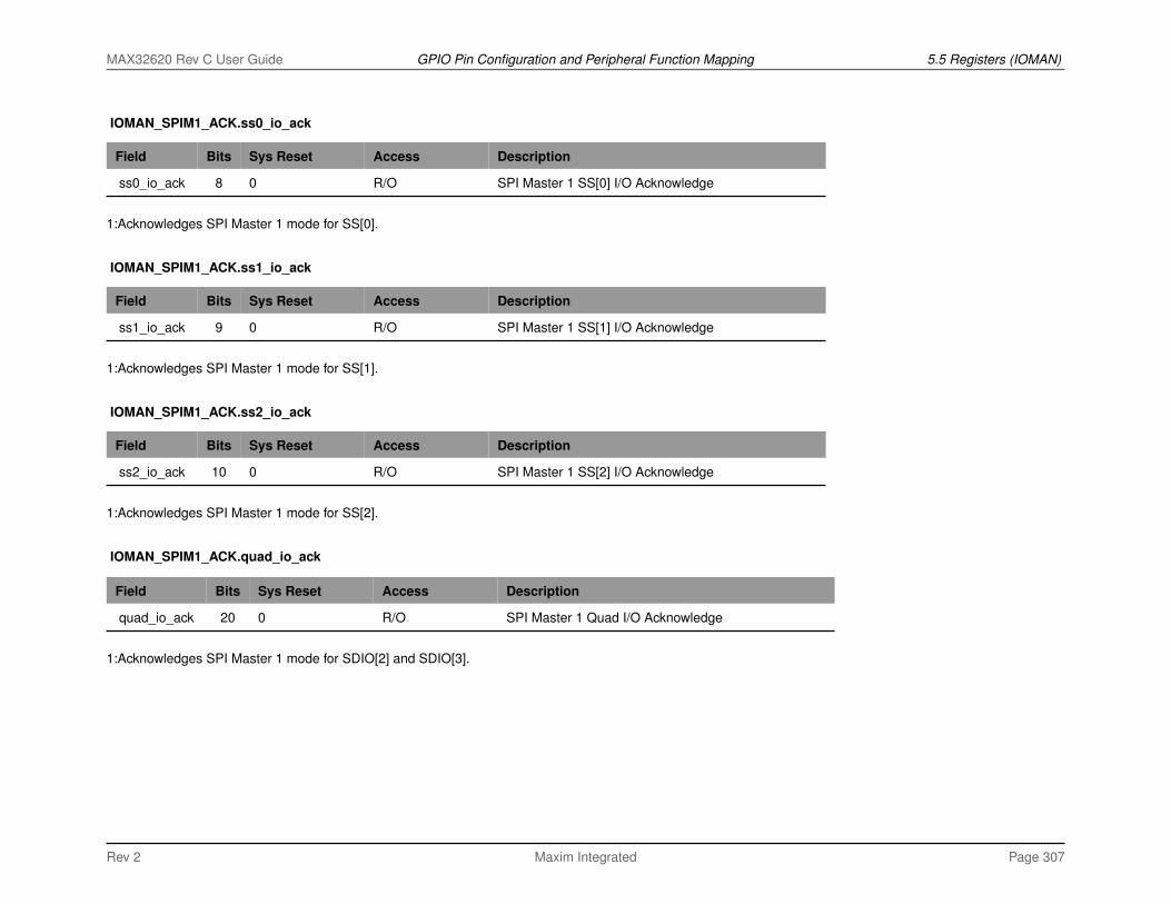
MAX32620 Rev C User Guide GPIO Pin Configuration and Peripheral Function Mapping 5.5 Registers (IOMAN)
IOMAN_SPIM1_ACK.ss0_io_ack
Field Bits Sys Reset Access Description
ss0_io_ack 8 0 R/O SPI Master 1 SS[0] I/O Acknowledge
1:Acknowledges SPI Master 1 mode for SS[0].
IOMAN_SPIM1_ACK.ss1_io_ack
Field Bits Sys Reset Access Description
ss1_io_ack 9 0 R/O SPI Master 1 SS[1] I/O Acknowledge
1:Acknowledges SPI Master 1 mode for SS[1].
IOMAN_SPIM1_ACK.ss2_io_ack
Field Bits Sys Reset Access Description
ss2_io_ack 10 0 R/O SPI Master 1 SS[2] I/O Acknowledge
1:Acknowledges SPI Master 1 mode for SS[2].
IOMAN_SPIM1_ACK.quad_io_ack
Field Bits Sys Reset Access Description
quad_io_ack 20 0 R/O SPI Master 1 Quad I/O Acknowledge
1:Acknowledges SPI Master 1 mode for SDIO[2] and SDIO[3].
Rev 2 Maxim Integrated Page 307

MAX32620 Rev C User Guide GPIO Pin Configuration and Peripheral Function Mapping 5.5 Registers (IOMAN)
IOMAN_SPIM1_ACK.fast_mode
Field Bits Sys Reset Access Description
fast_mode 24 0 R/O SPI Master 1 Fast Mode Acknowledge
Mirror of SPI Master 1 Fast Mode Request.
5.5.33 IOMAN_SPIM2_REQ
IOMAN_SPIM2_REQ.mapping_req
Field Bits Sys Reset Access Description
mapping_req 0 0 R/W SPI Master 2 I/O Mapping Select
• 0: Select pin mapping A for SPI Master 2 pins• 1: Select pin mapping B for SPI Master 2 pins
IOMAN_SPIM2_REQ.core_io_req
Field Bits Sys Reset Access Description
core_io_req 4 0 R/W SPI Master 2 Core I/O Request
• 0: No effect.• 1: Requests SPI Master 2 mode for SCK, SDIO[0] and SDIO[1].
IOMAN_SPIM2_REQ.ss0_io_req
Field Bits Sys Reset Access Description
ss0_io_req 8 0 R/W SPI Master 2 SS[0] I/O Request
• 0: No effect.• 1: Requests SPI Master 2 mode for SS[0].
Rev 2 Maxim Integrated Page 308

MAX32620 Rev C User Guide GPIO Pin Configuration and Peripheral Function Mapping 5.5 Registers (IOMAN)
IOMAN_SPIM2_REQ.ss1_io_req
Field Bits Sys Reset Access Description
ss1_io_req 9 0 R/W SPI Master 2 SS[1] I/O Request
• 0: No effect.• 1: Requests SPI Master 2 mode for SS[1].
IOMAN_SPIM2_REQ.ss2_io_req
Field Bits Sys Reset Access Description
ss2_io_req 10 0 R/W SPI Master 2 SS[2] I/O Request
• 0: No effect.• 1: Requests SPI Master 2 mode for SS[2].
IOMAN_SPIM2_REQ.sr0_io_req
Field Bits Sys Reset Access Description
sr0_io_req 16 0 R/W SPI Master 2 SR[0] I/O Request
• 0: No effect.• 1: Requests SPI Master 2 mode for SR[0].
IOMAN_SPIM2_REQ.sr1_io_req
Field Bits Sys Reset Access Description
sr1_io_req 17 0 R/W SPI Master 2 SR[1] I/O Request
• 0: No effect.• 1: Requests SPI Master 2 mode for SR[1].
Rev 2 Maxim Integrated Page 309

MAX32620 Rev C User Guide GPIO Pin Configuration and Peripheral Function Mapping 5.5 Registers (IOMAN)
IOMAN_SPIM2_REQ.quad_io_req
Field Bits Sys Reset Access Description
quad_io_req 20 0 R/W SPI Master 2 Quad I/O Request
• 0: No effect.• 1: Requests SPI Master 2 mode for SDIO[2] and SDIO[3].
IOMAN_SPIM2_REQ.fast_mode
Field Bits Sys Reset Access Description
fast_mode 24 0 R/W SPI Master 2 Fast Mode Request
1:Enables faster pad output transitions.
5.5.34 IOMAN_SPIM2_ACK
IOMAN_SPIM2_ACK.mapping_ack
Field Bits Sys Reset Access Description
mapping_ack 0 0 R/O SPI Master 2 I/O Mapping Acknowledge
Mirror of SPI Master 2 I/O Mapping Select value.
IOMAN_SPIM2_ACK.core_io_ack
Field Bits Sys Reset Access Description
core_io_ack 4 0 R/O SPI Master 2 Core I/O Acknowledge
1:Acknowledges SPI Master 2 mode for SCK, SDIO[0] and SDIO[1].
Rev 2 Maxim Integrated Page 310

MAX32620 Rev C User Guide GPIO Pin Configuration and Peripheral Function Mapping 5.5 Registers (IOMAN)
IOMAN_SPIM2_ACK.ss0_io_ack
Field Bits Sys Reset Access Description
ss0_io_ack 8 0 R/O SPI Master 2 SS[0] I/O Acknowledge
1:Acknowledges SPI Master 2 mode for SS[0].
IOMAN_SPIM2_ACK.ss1_io_ack
Field Bits Sys Reset Access Description
ss1_io_ack 9 0 R/O SPI Master 2 SS[1] I/O Acknowledge
1:Acknowledges SPI Master 2 mode for SS[1].
IOMAN_SPIM2_ACK.ss2_io_ack
Field Bits Sys Reset Access Description
ss2_io_ack 10 0 R/O SPI Master 2 SS[2] I/O Acknowledge
1:Acknowledges SPI Master 2 mode for SS[2].
IOMAN_SPIM2_ACK.sr0_io_req
Field Bits Sys Reset Access Description
sr0_io_req 16 0 R/O SPI Master 2 SR[0] I/O Acknowledge
1:Acknowledges SPI Master 2 mode for SR[0].
Rev 2 Maxim Integrated Page 311

MAX32620 Rev C User Guide GPIO Pin Configuration and Peripheral Function Mapping 5.5 Registers (IOMAN)
IOMAN_SPIM2_ACK.sr1_io_req
Field Bits Sys Reset Access Description
sr1_io_req 17 0 R/O SPI Master 2 SR[1] I/O Acknowledge
1:Acknowledges SPI Master 2 mode for SR[1].
IOMAN_SPIM2_ACK.quad_io_ack
Field Bits Sys Reset Access Description
quad_io_ack 20 0 R/O SPI Master 2 Quad I/O Acknowledge
1:Acknowledges SPI Master 2 mode for SDIO[2] and SDIO[3].
IOMAN_SPIM2_ACK.fast_mode
Field Bits Sys Reset Access Description
fast_mode 24 0 R/O SPI Master 2 Fast Mode Acknowledge
Mirror of SPI Master 2 Fast Mode Request.
5.5.35 IOMAN_SPIB_REQ
IOMAN_SPIB_REQ.core_io_req
Field Bits Sys Reset Access Description
core_io_req 4 0 R/W Reserved
Reserved; do not modify the value of this field.
Rev 2 Maxim Integrated Page 312

MAX32620 Rev C User Guide GPIO Pin Configuration and Peripheral Function Mapping 5.5 Registers (IOMAN)
IOMAN_SPIB_REQ.quad_io_req
Field Bits Sys Reset Access Description
quad_io_req 8 0 R/W Reserved
Reserved; do not modify the value of this field.
IOMAN_SPIB_REQ.fast_mode
Field Bits Sys Reset Access Description
fast_mode 12 0 R/W Reserved
Reserved; do not modify the value of this field.
5.5.36 IOMAN_SPIB_ACK
IOMAN_SPIB_ACK.core_io_ack
Field Bits Sys Reset Access Description
core_io_ack 4 0 R/O Reserved
Reserved; do not modify the value of this field.
IOMAN_SPIB_ACK.quad_io_ack
Field Bits Sys Reset Access Description
quad_io_ack 8 0 R/O Reserved
Reserved; do not modify the value of this field.
Rev 2 Maxim Integrated Page 313

MAX32620 Rev C User Guide GPIO Pin Configuration and Peripheral Function Mapping 5.5 Registers (IOMAN)
IOMAN_SPIB_ACK.fast_mode
Field Bits Sys Reset Access Description
fast_mode 12 0 R/O Reserved
Reserved; do not modify the value of this field.
5.5.37 IOMAN_OWM_REQ
IOMAN_OWM_REQ.mapping_req
Field Bits Sys Reset Access Description
mapping_req 4 0 R/W 1-Wire Line I/O Request
1:Requests 1-Wire line mode for OWD.
IOMAN_OWM_REQ.epu_io_req
Field Bits Sys Reset Access Description
epu_io_req 5 0 R/W External Pullup Control Line I/O Request
1:Requests 1-Wire external pullup control mode for EPU.
5.5.38 IOMAN_OWM_ACK
IOMAN_OWM_ACK.mapping_ack
Field Bits Sys Reset Access Description
mapping_ack 4 0 R/W 1-Wire Line I/O Acknowledge
1:Acknowledges 1-Wire line mode for OWD.
Rev 2 Maxim Integrated Page 314

MAX32620 Rev C User Guide GPIO Pin Configuration and Peripheral Function Mapping 5.5 Registers (IOMAN)
IOMAN_OWM_ACK.epu_io_ack
Field Bits Sys Reset Access Description
epu_io_ack 5 0 R/W External Pullup Control Line I/O Acknowledge
1:Acknowledges 1-Wire external pullup control mode for EPU.
5.5.39 IOMAN_SPIS_REQ
IOMAN_SPIS_REQ.core_io_req
Field Bits Sys Reset Access Description
core_io_req 4 0 R/W SPI Slave Core I/O Request
• 0: No effect.• 1: Requests SPI Slave mode for SCK, SSEL, SDIO[0] and SDIO[1].
IOMAN_SPIS_REQ.quad_io_req
Field Bits Sys Reset Access Description
quad_io_req 8 0 R/W SPI Slave Quad I/O Request
1:Requests SPI Slave mode for SDIO[2] and SDIO[3].
IOMAN_SPIS_REQ.fast_mode
Field Bits Sys Reset Access Description
fast_mode 12 0 R/W SPI Slave Fast Mode Request
Rev 2 Maxim Integrated Page 315

MAX32620 Rev C User Guide GPIO Pin Configuration and Peripheral Function Mapping 5.5 Registers (IOMAN)
5.5.40 IOMAN_SPIS_ACK
IOMAN_SPIS_ACK.core_io_ack
Field Bits Sys Reset Access Description
core_io_ack 4 0 R/O SPI Slave Core I/O Acknowledge
IOMAN_SPIS_ACK.quad_io_ack
Field Bits Sys Reset Access Description
quad_io_ack 8 0 R/O SPI Slave Quad I/O Acknowledge
IOMAN_SPIS_ACK.fast_mode
Field Bits Sys Reset Access Description
fast_mode 12 0 R/O SPI Slave Fast Mode Acknowledge
5.5.41 IOMAN_USE_VDDIOH_0
Sys Reset Access Description
0 R/W Enable VDDIOH Register 0
This register selects the I/O supply rail to be used (VDDIO or VDDIOH) for GPIO pins P0.0 through P3.7. For each bit set to 0 (the default value), the correspondingGPIO pin will use VDDIO as its supply rail. For each bit set to 1, the GPIO pin will use VDDIOH as its supply rail.
• bit 0: setting for P0.0• bit 1: setting for P0.1 ..• bit 7: setting for P0.7• bit 8: setting for P1.0 ..• bit 15: setting for P1.7• bit 16: setting for P2.0 ..• bit 23: setting for P2.7• bit 24: setting for P3.0 ..
Rev 2 Maxim Integrated Page 316

MAX32620 Rev C User Guide GPIO Pin Configuration and Peripheral Function Mapping 5.5 Registers (IOMAN)
• bit 31: setting for P3.7
5.5.42 IOMAN_USE_VDDIOH_1
Sys Reset Access Description
0 R/W Enable VDDIOH Register 1
This register selects the I/O supply rail to be used (VDDIO or VDDIOH) for GPIO pins P4.0 through P6.0. For each bit set to 0 (the default value), the correspondingGPIO pin will use VDDIO as its supply rail. For each bit set to 1, the GPIO pin will use VDDIOH as its supply rail.
• bit 0: setting for P4.0• bit 1: setting for P4.1 ..• bit 7: setting for P4.7• bit 8: setting for P5.0 ..• bit 15: setting for P5.7• bit 16: setting for P6.0• bits 17 through 31: unused.
5.5.43 IOMAN_PAD_MODE
IOMAN_PAD_MODE.slow_mode
Field Bits Sys Reset Access Description
slow_mode 0 0 R/W Reserved
Reserved. Do not modify the value of this field.
IOMAN_PAD_MODE.alt_rcvr_mode
Field Bits Sys Reset Access Description
alt_rcvr_mode 1 0 R/W Reserved
Reserved. Do not modify the value of this field.
Rev 2 Maxim Integrated Page 317

MAX32620 Rev C User Guide Peripheral Management Unit (PMU)
6 Peripheral Management Unit (PMU)
6.1 Overview
The Peripheral Management Unit (PMU) on the MAX32620 is a DMA-based linked list processing engine. It allows low-overhead peripheral operations to beperformed without the CPU, significantly reducing overall power consumption.
The PMU can perform operations and data transfers involving internal and external memory, as well as AHB/APB memory mapped peripherals. These operationscan be performed while the CPU is active (LP3:RUN) in order to reduce the processing load on the CPU and allow the application to focus on other tasks, or whilethe CPU is in sleep mode (LP2:PMU) in order to reduce power consumption.
Key features of the PMU engine include:• Six independent channels with round-robin scheduling to allow multiple parallel operations without requiring use of the CPU• Suited for moving data to/from memory and peripherals• Integrated AHB bus master• Operates based on descriptor sequences located in memory• Able to respond to peripheral interrupts and event flags without CPU interrupt handling• May trigger interrupts to the CPU if needed• Utilizing the PMU while the CPU is in sleep mode (LP2:PMU) reduces system power consumption
Rev 2 Maxim Integrated Page 318

MAX32620 Rev C User Guide Peripheral Management Unit (PMU) 6.1 Overview
Figure 6.1: PMU Block Diagram
Rev 2 Maxim Integrated Page 319

MAX32620 Rev C User Guide Peripheral Management Unit (PMU) 6.2 PMU Operation
6.2 PMU Operation
The PMU is a six-channel, programmable DMA controller that executes user-defined PMU descriptor sequences. These descriptor sequences reside in theMAX32620 memory space. Acting as an AHB master, the PMU can access any memory address in either the AHB or APB memory spaces. Each of the sixchannels runs independently and shares accesses to the AHB/APB address space using an internal round-robin arbiter, on a descriptor-by-descriptor basis, withpriority encoding. Priority ranges from channel one with the highest priority and channel six with the lowest priority. The PMU runs from the PMU peripheral clock(per_clk_pmu) which runs at the same frequency as the CPU core (scaling configured by CLKMAN_SYS_CLK_CTRL_0_CM4).
6.2.1 PMU Operation Descriptors
Each active PMU channel independently executes a PMU descriptor sequence specific to that channel. A descriptor sequence is made up of one or more PMUdescriptors, with each descriptor consisting of a 32-bit op code doubleword and one or more operand doublewords, as described below. When configuring a PMUchannel for operation, the user specifies the address of the first PMU descriptor in the descriptor sequence. With the exception of descriptors that may change thenext descriptor address (such as JUMP, LOOP and BRANCH), the PMU channel executes descriptors sequentially.
Descriptor execution for a given PMU channel automatically halts when a descriptor containing (STOP == 1) is executed or an error condition is encountered. APMU channel can also be halted manually by clearing the enable bit in the channel’s PMUn_CFG register. There is no limit to the number of descriptors that can beexecuted in a descriptor sequence.
Each PMU channel has two control registers that control the operation of the channel. The descriptor address register PMUn_DSCADR is used to set the 32-bitaddress of the first descriptor in the descriptor sequence. This register is also updated with the current descriptor address as the PMU channel executes eachdescriptor in the sequence. The channel configuration register PMUn_CFG is used to start and stop descriptor execution for that channel. This register also reportsstatus and error information.
6.2.2 Setup and PMU Channel Start
Before using a PMU channel, the user must load the PMU descriptor sequence into SRAM or internal/external flash memory. Once the descriptor sequence hasbeen written to memory, the user must set the starting address of the first descriptor using the PMUn_DSCADR register. To start channel execution, set the enablebit in the channel’s PMUn_CFG register to 1. The PMU channel engine will then fetch the first descriptor in the sequence and begin processing.
Upon completion of the first PMU descriptor, subsequent descriptors are fetched sequentially from memory unless the descriptor address is changed by a JUMP,LOOP, or BRANCH descriptor. As each PMU descriptor is executed, the PMUn_DSCADR register is updated with the address of the next descriptor to be executedby the channel.
The end of the descriptor sequence is defined by a descriptor with the STOP bit set. Once the PMU channel executes a descriptor with (STOP == 1), the channelwill halt execution. When this occurs, the enable bit will be cleared, and the PMUn_CFG.ll_stopped bit will be set to 1 by hardware to indicate the reason why thechannel stopped executing.
Rev 2 Maxim Integrated Page 320

MAX32620 Rev C User Guide Peripheral Management Unit (PMU) 6.3 PMU Descriptor Details
6.2.3 PMU Channel Arbitration
The PMU is an AHB bus master, and allows each of the channels access to the AHB/APB memory space. Arbitration between PMU channels for access to the busmaster is performed by a round-robin scheduler, on a descriptor-by-descriptor basis, with priority encoding.
For example: If three PMU channels are active, execution would start with channel 1, descriptor 1; then proceed to channel 2, descriptor 1; channel 3, descriptor 1;channel 1, descriptor 2; etc. If a channel is temporarily blocked due to a flow control condition, execution will move to the next active channel. For example, executionof a WAIT, POLL, or TRANSFER descriptor may cause a channel to stay at the same execution address for some time while the descriptor operation completes.But this does not block the round-robin arbitration for other active channels; these channels will continue executing in turn while the first channel completes its longoperation.
6.3 PMU Descriptor Details
There are eight descriptor types which can be included in a PMU descriptor sequence. Each descriptor consists of one 32-bit descriptor op code doubleword andfrom one to four 32-bit descriptor parameter doublewords. The number of parameters varies according to the descriptor type, but all descriptors of a given type willalways have the same number of parameters.
The available descriptor types and the total length of each type (in doublewords) is as follows:• MOVE : 3 doublewords• WRITE : 4 doublewords• WAIT : 4 doublewords• JUMP : 2 doublewords• LOOP : 2 doublewords• BRANCH : 5 doublewords• POLL : 5 doublewords• TRANSFER: 4 doublewords
6.3.1 MOVE Descriptor
The MOVE descriptor is used to copy a user-specified number of bytes from a read address location to a write address location. Read and write addresses may be ineither the AHB or APB memory space. The read address and write address are specified (independently from each other) to be either fixed or incrementing. A fixedread/write address is used when reading from or writing to a FIFO or similar access point where the address does not need to change. An incrementing read/writeaddress is used when reading from or writing to a standard memory structure such as the internal SRAM, or an internal working memory for a peripheral such as theMAA. AHB accesses may be 8-bit, 16-bit or 32-bit width as supported by the particular area of memory or the peripheral FIFO being accessed. All APB accessesare restricted to 32-bit width only.
Rev 2 Maxim Integrated Page 321

MAX32620 Rev C User Guide Peripheral Management Unit (PMU) 6.3 PMU Descriptor Details
Figure 6.2: PMU MOVE Descriptor
6.3.1.1 OP_CODE
This three-bit field is set to 000b to define the descriptor as a MOVE descriptor.
6.3.1.2 INT
If this bit is set to 1, the interrupt flag for the current channel will be set to 1 after the channel completes execution of this descriptor.
6.3.1.3 STOP
If this bit is set to 1, once the PMU channel completes execution of this descriptor, the PMU channel will halt execution. When this occurs, the ll_stopped flag for thecurrent channel will be set to 1 by hardware to indicate that the PMU descriptor sequence has completed execution.
6.3.1.4 RD_SIZE, WR_SIZE
These fields determine the width of memory access that will be used on the read side (source) and write side (destination) of the data transfer. Note that any accessto APB register space requires the width to be 32-bit only; use of 8-bit or 16-bit width when accessing APB space will result in a bus error. When accessing AHB
Rev 2 Maxim Integrated Page 322

MAX32620 Rev C User Guide Peripheral Management Unit (PMU) 6.3 PMU Descriptor Details
areas, the widths for the read and write sides can be different; the PMU channel controller will automatically handle data packing/unpacking as needed.
RD SIZE WR SIZE Operation
00b 00b Perform 8-bit reads and 8-bit writes
00b 01b Perform 8-bit reads and pack data into 16-bit writes
00b 10b Perform 8-bit reads and pack data into 32-bit writes
01b 00b Perform 16-bit reads and unpack into 8-bit writes
01b 01b Perform 16-bit reads and writes
01b 10b Perform 16-bit reads and pack data into 32-bitwrites
10b 00b Perform 32-bit reads and unpack data into 8-bitwrites
10b 01b Perform 32-bit reads and unpack data into 16-bitwrites
10b 10b Perform 32-bit reads and writes
XX 11b (Reserved)
11b XX (Reserved)
6.3.1.5 RD_INC
If this bit is set to 0, then read address auto-incrementing is disabled. This means that the same read address value will be used for all reads in this data transfersequence. This is a useful setting when reading from FIFOs, where a single address location must be read repeatedly to unload data.
If this bit is set to 1, then read address auto-incrementing is enabled. This means that every read access in the data transfer will cause the read address pointerto automatically post-increment, based on the RD_SIZE width. For example, if RD_SIZE is set to 01b, then following each 16-bit read access in the data transfersequence, the read address pointer will be incremented by 2. This is a useful setting when accessing SRAM or memory register files, where a different address isused to access each location in the memory area.
Note When executing a MOVE descriptor with (CONT == 1), the RD_INC bit must be set to the same value as the RD_INC bit from the previously-executedMOVE descriptor with (CONT == 0).
Rev 2 Maxim Integrated Page 323

MAX32620 Rev C User Guide Peripheral Management Unit (PMU) 6.3 PMU Descriptor Details
6.3.1.6 WR_INC
If this bit is set to 0, then write address auto-incrementing is disabled. This means that the same write address value will be used for all writes in this data transfersequence. This is a useful setting when writing to FIFOs or similar locations, where a single address location must be written to repeatedly to load or process data.
If this bit is set to 1, then write address auto-incrementing is enabled. This means that every write access in the data transfer will cause the write address pointerto automatically post-increment, based on the WR_SIZE width. For example, if WR_SIZE is set to 00b, then following each 8-bit write access in the data transfersequence, the write address pointer will be incremented by 1. This is a useful setting when accessing SRAM or memory register files, where a different address isused to access each location in the memory area.
Note When executing a MOVE descriptor with (CONT == 1), the WR_INC bit must be set to the same value as the WR_INC bit from the previously-executed MOVE descriptor with (CONT == 0).
6.3.1.7 CONT
Setting this bit to 1 allows a subsequent MOVE descriptor to continue operation using the read address, write address, and RD_INC and WR_INC values definedby a previous MOVE descriptor. Before a MOVE descriptor with (CONT == 1) can be executed, a previous MOVE descriptor with (CONT == 0) must be executed toinitialize READ_ADDRESS, WRITE_ADDRESS, RD_INC and WR_INC.
If this bit is set to 0, the MOVE descriptor will not rely on any existing read and write settings from a previous MOVE descriptor and instead will use its own values forthese fields.
6.3.1.8 TRANSFER_LENGTH
Total length of transfer (in bytes) from the read address to the write address.
6.3.1.9 WRITE_ADDRESS
This field specifies the write address used for the data transfer (or if WR_INC == 1, the starting write address).
Note When executing a MOVE descriptor with (CONT == 1), the WRITE_ADDRESS field must be set to the same value as the WRITE_ADDRESS fieldfrom the previously-executed MOVE descriptor with (CONT == 0). In this case, the contents of the WRITE_ADDRESS field in the MOVE descriptorwith (CONT == 1) will not be used, but the two fields must still be set to identical values for proper operation.
6.3.1.10 READ_ADDRESS
This field specifies the read address used for the data transfer (or if RD_INC == 1, the starting read address).
Rev 2 Maxim Integrated Page 324

MAX32620 Rev C User Guide Peripheral Management Unit (PMU) 6.3 PMU Descriptor Details
Note When executing a MOVE descriptor with (CONT == 1), the READ_ADDRESS field must be set to the same value as the READ_ADDRESS fieldfrom the previously-executed MOVE descriptor with (CONT == 0). In this case, the contents of the READ_ADDRESS field in the MOVE descriptorwith (CONT == 1) will not be used, but the two fields must still be set to identical values for proper operation.
6.3.2 WRITE Descriptor
The WRITE descriptor will cause the value specified by WRITE_VALUE to be written to the byte address location specified by WRITE_ADDRESS. Only bits set inthe write mask field WRITE_MASK will be modified. This allows the user to set or clear individual bits in a 32-bit field. Write accesses may be in either the AHB orAPB memory space. All accesses must be 32-bit width only.
Figure 6.3: PMU WRITE Descriptor
6.3.2.1 OP_CODE
This three-bit field is set to 001b to define the descriptor as a WRITE descriptor.
Rev 2 Maxim Integrated Page 325

MAX32620 Rev C User Guide Peripheral Management Unit (PMU) 6.3 PMU Descriptor Details
6.3.2.2 INT
If this bit is set to 1, the interrupt flag for the current channel will be set to 1 after the channel completes execution of this descriptor.
6.3.2.3 STOP
If this bit is set to 1, once the PMU channel completes execution of this descriptor, the PMU channel will halt execution. When this occurs, the ll_stopped flag for thecurrent channel will be set to 1 by hardware to indicate that the PMU descriptor sequence has completed execution.
6.3.2.4 WRITE_METHOD
The value of this field determines how the three input parameters for this operation (the WRITE_VALUE and WRITE_MASK in the descriptor, along with the currentdata value read from the WRITE_ADDRESS location) will be combined to determine the final value that is written back to the WRITE_ADDRESS destination.Depending on the type of WRITE_METHOD used, the WRITE_VALUE and WRITE_MASK parameters may or may not be used when determining the final valueoutput. The value read from the WRITE_ADDRESS location (labeled in the table below as Read_Value) will always be used as part of this operation.
WRITE_METHOD WRITE_VALUE Used Mask Used Value Written to WRITE_ADDRESSLocation
0000b Yes Yes (Read_Value AND (NOTWRITE_MASK)) OR WRITE_VALUE
0001b No No Read_Value + 1 (unsigned)
0010b No No Read_Value - 1 (unsigned)
0011b No No Read_Value >> 1 (shifted right onebit, leftmost bit replaced with zero)
0100b No No Read_Value << 1 (shifted left onebit, rightmost bit replaced with zero)
0101b No No Read_Value rotated right one bit, bit 0rotates around to bit position 31
0110b No No Read_Value rotated left one bit, bit 31rotates around to bit position 0
0111b No No NOT Read_Value
Rev 2 Maxim Integrated Page 326

MAX32620 Rev C User Guide Peripheral Management Unit (PMU) 6.3 PMU Descriptor Details
1000b No Yes Read_Value XOR WRITE_MASK (in-vert bits at positions set to 1 inWRITE_MASK)
1001b No Yes Read_Value OR WRITE_MASK(set bits at positions set to 1 inWRITE_MASK)
1010b No Yes Read_Value AND WRITE_MASK(clear bits at positions set to 0 inWRITE_MASK)
6.3.2.5 WRITE_ADDRESS
Address of location to be written to.
6.3.2.6 WRITE_VALUE
Value that will be written to the write location (only where the matching bits in the WRITE_MASK are also set to 1).
6.3.2.7 WRITE_MASK
This field determines which bits in WRITE_VALUE will be written to the destination. Bits in WRITE_MASK set to 1 indicate positions where new data will be written;bits set to 0 indicate positions where the data will not be changed.
6.3.3 WAIT Descriptor
The WAIT descriptor will cause the PMU channel to pause execution (remaining at the WAIT descriptor location) until one or more of the interrupt sources selected bythe interrupt mask are set. If all bits in INT_MASK are zero, the WAIT descriptor will complete immediately (following any delay specified by WAIT + WAIT_COUNT)and the PMU channel will continue executing the descriptor sequence.
Rev 2 Maxim Integrated Page 327

MAX32620 Rev C User Guide Peripheral Management Unit (PMU) 6.3 PMU Descriptor Details
Figure 6.4: PMU WAIT Descriptor
6.3.3.1 OP_CODE
This three-bit field is set to 010b to define the descriptor as a WAIT descriptor.
6.3.3.2 INT
If this bit is set to 1, the interrupt flag for the current channel will be set to 1 after the channel completes execution of this descriptor.
6.3.3.3 STOP
If this bit is set to 1, once the PMU channel completes execution of this descriptor, the PMU channel will halt execution. When this occurs, the ll_stopped flag for thecurrent channel will be set to 1 by hardware to indicate that the PMU descriptor sequence has completed execution.
Rev 2 Maxim Integrated Page 328

MAX32620 Rev C User Guide Peripheral Management Unit (PMU) 6.3 PMU Descriptor Details
6.3.3.4 WAIT
If this bit is set to 1, after the condition specified by INT_MASK has occurred, the PMU channel will delay for the number of PMU module clock specified byWAIT_COUNT before continuing on.
6.3.3.5 SEL
This bit determines which group of PMU interrupt sources will be used by the WAIT descriptor. If the SEL bit is set to 0, the first group will be used. If the SEL bit isset to 1, the second group will be used.
6.3.3.6 WAIT_COUNT
When (WAIT == 1), this field specifies the number of PMU module clocks for the PMU channel to delay after the INT_MASK condition has been satisfied.
6.3.3.7 INT_MASK
The interrupt mask field corresponds to the following interrupt sources available to the PMU.
The following interrupts are only used with the WAIT descriptor when the SEL bit is set to 0. These interrupts are generated by the Peripheral FIFOs automaticallyas listed below based on FIFO configuration registers. They do not require the user to clear or enable the interrupt source; they are self-clearing and enabled by theappropriate FIFO configuration registers as shown in the table below.
PMU FIFO Interrupt Sources for WAIT (when SEL=0) - Peripheral FIFO Generated
Bit Source Interrupt Set Condition Interrupt Clear Condition
0 UART0 TX FIFO Almost Empty Set when the TX FIFO level fallsbelow the user defined threshold inUART0_TX_FIFO_CTRL.fifo_ae_lvl
Self-clears when the TX FIFO level isabove this threshold
1 UART0 RX FIFO Almost Full Set when the RX FIFO level isabove the user defined threshold inUART0_RX_FIFO_CTRL.fifo_af_lvl
Self-clears when RX FIFO level fallsbelow this threshold
2 UART1 TX FIFO Almost Empty Set when the TX FIFO level fallsbelow the user defined threshold inUART1_TX_FIFO_CTRL.fifo_ae_lvl
Self-clears when the TX FIFO level isabove this threshold
Rev 2 Maxim Integrated Page 329

MAX32620 Rev C User Guide Peripheral Management Unit (PMU) 6.3 PMU Descriptor Details
3 UART1 RX FIFO Almost Full Set when the RX FIFO level isabove the user defined threshold inUART1_RX_FIFO_CTRL.fifo_af_lvl
Self-clears when RX FIFO level fallsbelow this threshold
4 UART2 TX FIFO Almost Empty Set when the TX FIFO level fallsbelow the user defined threshold inUART2_TX_FIFO_CTRL.fifo_ae_lvl
Self-clears when the TX FIFO level isabove this threshold
5 UART2 RX FIFO Almost Full Set when the RX FIFO level isabove the user defined threshold inUART2_RX_FIFO_CTRL.fifo_af_lvl
Self-clears when RX FIFO level fallsbelow this threshold
6 UART3 TX FIFO Almost Empty Set when the TX FIFO level fallsbelow the user defined threshold inUART3_TX_FIFO_CTRL.fifo_ae_lvl
Self-clears when the TX FIFO level isabove this threshold
7 UART3 RX FIFO Almost Full Set when the RX FIFO level isabove the user defined threshold inUART3_RX_FIFO_CTRL.fifo_af_lvl
Self-clears when RX FIFO level fallsbelow this threshold
8 SPIM0 TX FIFO Almost Empty Set when the TX FIFO level fallsbelow the user defined threshold inSPIM0_FIFO_CTRL.tx_fifo_ae_lvl
Self-clears when the TX FIFO level isabove this threshold
9 SPIM0 RX FIFO Almost Full Set when the RX FIFO level isabove the user defined threshold inSPIM0_FIFO_CTRL.rx_fifo_af_lvl
Self-clears when the RX FIFO levelfalls below this threshold
10 SPIM1 TX FIFO Almost Empty Set when the TX FIFO level fallsbelow the user defined threshold inSPIM1_FIFO_CTRL.tx_fifo_ae_lvl
Self-clears when the TX FIFO level isabove this threshold
11 SPIM1 RX FIFO Almost Full Set when the RX FIFO level isabove the user defined threshold inSPIM1_FIFO_CTRL.rx_fifo_af_lvl
Self-clears when the RX FIFO levelfalls below this threshold
12 SPIM2 TX FIFO Almost Empty Set when the TX FIFO level fallsbelow the user defined threshold inSPIM2_FIFO_CTRL.tx_fifo_ae_lvl
Self-clears when the TX FIFO level isabove this threshold
13 SPIM2 RX FIFO Almost Full Set when the RX FIFO level isabove the user defined threshold inSPIM2_FIFO_CTRL.rx_fifo_af_lvl
Self-clears when the RX FIFO levelfalls below this threshold
Rev 2 Maxim Integrated Page 330

MAX32620 Rev C User Guide Peripheral Management Unit (PMU) 6.3 PMU Descriptor Details
14 I2CM0 TX FIFO Empty Set when no data is in the TX FIFO Self-clears when the TX FIFO con-tains at least one byte of data
15 I2CM0 RX FIFO Not Empty Set when the RX FIFO contains atleast one byte of data
Self-clears when no data is in the RXFIFO
16 I2CM1 TX FIFO Empty Set when no data is in the TX FIFO Self-clears when the TX FIFO con-tains at least one byte of data
17 I2CM1 RX FIFO Not Empty Set when the RX FIFO contains atleast one byte of data
Self-clears when no data is in the RXFIFO
18 I2CM2 TX FIFO Empty Set when no data is in the TX FIFO Self-clears when the TX FIFO con-tains at least one byte of data
19 I2CM2 RX FIFO Not Empty Set when the RX FIFO contains atleast one byte of data
Self-clears when no data is in the RXFIFO
The remaining interrupts (when SEL=0), shown below, must be enabled through the appropriate peripheral register and also cleared after the interrupt becomes set.
PMU Interrupt Event Table (when SEL=0) for WAIT Descriptor
Interrupt Bit Source Enable and Clear
20 SPIM0 rx_stalled OR tx_ready OR tx_stalled SPIM0_INTEN.rx_stalled,SPIM0_INTEN.tx_stalled orSPIM0_INTEN.tx_ready to enable;SPIM0_INTFL.rx_stalled, SPIM0_INTFL.tx_stalledor SPIM0_INTFL.tx_readyto clear (W1C)
21 SPIM1 rx_stalled OR tx_ready OR tx_stalled SPIM1_INTEN.rx_stalled,SPIM1_INTEN.tx_stalled orSPIM1_INTEN.tx_ready to enable;SPIM1_INTFL.rx_stalled, SPIM1_INTFL.tx_stalledor SPIM1_INTFL.tx_readyto clear (W1C)
22 SPIM2 rx_stalled OR tx_ready OR tx_stalled SPIM2_INTEN.rx_stalled,SPIM2_INTEN.tx_stalled orSPIM2_INTEN.tx_ready to enable;SPIM2_INTFL.rx_stalled, SPIM2_INTFL.tx_stalledor SPIM2_INTFL.tx_readyto clear (W1C)
23 Reserved Reserved
Rev 2 Maxim Integrated Page 331

MAX32620 Rev C User Guide Peripheral Management Unit (PMU) 6.3 PMU Descriptor Details
24 I2CM0 TX Finished I2CM0_INTEN.tx_done to enable,I2CM0_INTFL.tx_done to clear (W1C)
25 I2CM1 TX Finished I2CM1_INTEN.tx_done to enable,I2CM1_INTFL.tx_done to clear (W1C)
26 I2CM2 TX Finished I2CM2_INTEN.tx_done to enable,I2CM2_INTFL.tx_done to clear (W1C)
27 I2CS Byte(s) Updated Set one or more bits in I2CS_INTEN to enable,clear corresponding flags in I2CS_INTFL when set(W1C)
28 ADC Done ADC_INTR.adc_done_ie to enable,ADC_INTR.adc_done_if to clear (W1C)
29 ADC Ready ADC_INTR.adc_ref_ready_ie to enable,ADC_INTR.adc_ref_ready_if to clear (W1C)
30 ADC Sample Above High Limit ADC_INTR.adc_hi_limit_ie to enable,ADC_INTR.adc_hi_limit_if to clear (W1C)
31 ADC Sample Below Low Limit ADC_INTR.adc_lo_limit_ie to enable,ADC_INTR.adc_lo_limit_if to clear (W1C)
32 RTC Timer Match (Comparator 0) RTCTMR_INTEN.comp0 to enable,RTCTMR_FLAGS.comp0 to clear (W1C)
33 RTC Timer Match (Comparator 1) RTCTMR_INTEN.comp1 to enable,RTCTMR_FLAGS.comp1 to clear (W1C)
34 RTC Prescaler Interval RTCTMR_INTEN.prescale_comp to enable,RTCTMR_FLAGS.prescale_comp to clear (W1C)
35 RTC Timer Overflow RTCTMR_INTEN.overflow to enable,RTCTMR_FLAGS.overflow to clear (W1C)
36 Pulse Train 0 Disabled Does not require enable. This PMU interrupt sourceis set to 1 whenever pulse train 0 is disabled.
37 Pulse Train 1 Disabled Does not require enable. This PMU interrupt sourceis set to 1 whenever pulse train 1 is disabled.
38 Pulse Train 2 Disabled Does not require enable. This PMU interrupt sourceis set to 1 whenever pulse train 2 is disabled.
Rev 2 Maxim Integrated Page 332

MAX32620 Rev C User Guide Peripheral Management Unit (PMU) 6.3 PMU Descriptor Details
39 Pulse Train 3 Disabled Does not require enable. This PMU interrupt sourceis set to 1 whenever pulse train 3 is disabled.
40 Pulse Train 4 Disabled Does not require enable. This PMU interrupt sourceis set to 1 whenever pulse train 4 is disabled.
41 Pulse Train 5 Disabled Does not require enable. This PMU interrupt sourceis set to 1 whenever pulse train 5 is disabled.
42 Pulse Train 6 Disabled Does not require enable. This PMU interrupt sourceis set to 1 whenever pulse train 6 is disabled.
43 Pulse Train 7 Disabled Does not require enable. This PMU interrupt sourceis set to 1 whenever pulse train 7 is disabled.
44 Pulse Train 8 Disabled Does not require enable. This PMU interrupt sourceis set to 1 whenever pulse train 8 is disabled.
45 Pulse Train 9 Disabled Does not require enable. This PMU interrupt sourceis set to 1 whenever pulse train 9 is disabled.
46 Pulse Train 10 Disabled Does not require enable. This PMU interrupt sourceis set to 1 whenever pulse train 10 is disabled.
47 Pulse Train 11 Disabled Does not require enable. This PMU interrupt sourceis set to 1 whenever pulse train 11 is disabled.
48 Timer0 32-bit or 16-bit interrupts TMR0_INTEN.timer0 to enable,TMR0_INTFL.timer0 to clear
49 Timer1 32-bit or 16-bit interrupts TMR1_INTEN.timer0 to enable,TMR1_INTFL.timer0 to clear
50 Timer2 32-bit or 16-bit interrupts TMR2_INTEN.timer0 to enable,TMR2_INTFL.timer0 to clear
51 Timer3 32-bit or 16-bit interrupts TMR3_INTEN.timer0 to enable,TMR3_INTFL.timer0 to clear
52 Timer4 32-bit or 16-bit interrupts TMR4_INTEN.timer0 to enable,TMR4_INTFL.timer0 to clear
53 Timer5 32-bit or 16-bit interrupts TMR5_INTEN.timer0 to enable,TMR5_INTFL.timer0 to clear
Rev 2 Maxim Integrated Page 333

MAX32620 Rev C User Guide Peripheral Management Unit (PMU) 6.3 PMU Descriptor Details
54 Interrupt(s) on Port 0 GPIO GPIO_INT_MODE_P0.pin[7:0] to enable,GPIO_INTFL_P0.pin[7:0] to clear (W1C)
55 Interrupt(s) on Port 1 GPIO GPIO_INT_MODE_P1.pin[7:0] to enable,GPIO_INTFL_P1.pin[7:0] to clear (W1C)
56 Interrupt(s) on Port 2 GPIO GPIO_INT_MODE_P2.pin[7:0] to enable,GPIO_INTFL_P2.pin[7:0] to clear (W1C)
57 Interrupt(s) on Port 3 GPIO GPIO_INT_MODE_P3.pin[7:0] to enable,GPIO_INTFL_P3.pin[7:0] to clear (W1C)
58 Interrupt(s) on Port 4 GPIO GPIO_INT_MODE_P4.pin[7:0] to enable,GPIO_INTFL_P4.pin[7:0] to clear (W1C)
59 Interrupt(s) on Port 5 GPIO GPIO_INT_MODE_P5.pin[7:0] to enable,GPIO_INTFL_P5.pin[7:0] to clear (W1C)
60 Interrupt(s) on Port 6 GPIO GPIO_INT_MODE_P6.pin[7:0] to enable,GPIO_INTFL_P6.pin[7:0] to clear (W1C)
61 AES done AES_CTRL.inten to enable, AES_CTRL.intfl toclear (W1C)
62 MAA done (MAX32621 only) MAA_CTRL.inten to enable, MAA_CTRL.if_done toclear (W1C)
63 1-Wire Master Interrupt (Reset Done) OWM_INTEN.ow_reset_done to enable,OWM_INTFL.ow_reset_done to clear (W1C)
63 1-Wire Master Interrupt (TX Data Empty) OWM_INTEN.tx_data_empty to enable,OWM_INTFL.tx_data_empty to clear (W1C)
63 1-Wire Master Interrupt (RX Data Ready) OWM_INTEN.rx_data_ready to enable,OWM_INTFL.rx_data_ready to clear (W1C)
63 1-Wire Master Interrupt (Line Short) OWM_INTEN.line_short to enable,OWM_INTFL.line_short to clear (W1C)
63 1-Wire Master Interrupt (Line Low) OWM_INTEN.line_low to enable,OWM_INTFL.line_low to clear (W1C)
When SEL=1, all interrupts used by the WAIT descriptor must be enabled and cleared manually by firmware; there are no self-clearing interrupt sources in this mode.
PMU Interrupt Event Table (when SEL=1) for WAIT Descriptor
Rev 2 Maxim Integrated Page 334

MAX32620 Rev C User Guide Peripheral Management Unit (PMU) 6.3 PMU Descriptor Details
Interrupt Bit Source Enable and Clear
0 Reserved Reserved
1 Reserved Reserved
2 Pulse Train 12 Disabled Does not require enable. This PMU interrupt sourceis set to 1 whenever pulse train 12 is disabled. Auto-clears.
3 Pulse Train 13 Disabled Does not require enable. This PMU interrupt sourceis set to 1 whenever pulse train 13 is disabled. Auto-clears.
4 Pulse Train 14 Disabled Does not require enable. This PMU interrupt sourceis set to 1 whenever pulse train 14 is disabled. Auto-clears.
5 Pulse Train 15 Disabled Does not require enable. This PMU interrupt sourceis set to 1 whenever pulse train 15 is disabled. Auto-clears.
6 Pulse Train 0 Stopped PTG_INTEN.pt0 to enable, PTG_INTFL.pt0 to clear
7 Pulse Train 1 Stopped PTG_INTEN.pt1 to enable, PTG_INTFL.pt1 to clear
8 Pulse Train 2 Stopped PTG_INTEN.pt2 to enable, PTG_INTFL.pt2 to clear
9 Pulse Train 3 Stopped PTG_INTEN.pt3 to enable, PTG_INTFL.pt3 to clear
10 Pulse Train 4 Stopped PTG_INTEN.pt4 to enable, PTG_INTFL.pt4 to clear
11 Pulse Train 5 Stopped PTG_INTEN.pt5 to enable, PTG_INTFL.pt5 to clear
12 Pulse Train 6 Stopped PTG_INTEN.pt6 to enable, PTG_INTFL.pt6 to clear
13 Pulse Train 7 Stopped PTG_INTEN.pt7 to enable, PTG_INTFL.pt7 to clear
14 Pulse Train 8 Stopped PTG_INTEN.pt8 to enable, PTG_INTFL.pt8 to clear
15 Pulse Train 9 Stopped PTG_INTEN.pt9 to enable, PTG_INTFL.pt9 to clear
16 Pulse Train 10 Stopped PTG_INTEN.pt10 to enable, PTG_INTFL.pt10 toclear
17 Pulse Train 11 Stopped PTG_INTEN.pt11 to enable, PTG_INTFL.pt11 toclear
Rev 2 Maxim Integrated Page 335

MAX32620 Rev C User Guide Peripheral Management Unit (PMU) 6.3 PMU Descriptor Details
18 Pulse Train 12 Stopped PTG_INTEN.pt12 to enable, PTG_INTFL.pt12 toclear
19 Pulse Train 13 Stopped PTG_INTEN.pt13 to enable, PTG_INTFL.pt13 toclear
20 Pulse Train 14 Stopped PTG_INTEN.pt14 to enable, PTG_INTFL.pt14 toclear
21 Pulse Train 15 Stopped PTG_INTEN.pt15 to enable, PTG_INTFL.pt15 toclear
22 SPIS TX FIFO Almost Empty SPIS_INTEN.tx_fifo_ae to enable,SPIS_INTFL.tx_fifo_ae to clear (W1C)
23 SPIS RX FIFO Almost Full SPIS_INTEN.rx_fifo_af to enable,SPIS_INTFL.rx_fifo_af to clear (W1C)
24 SPIS TX FIFO No Data SPIS_INTEN.tx_no_data to enable,SPIS_INTFL.tx_no_data to clear (W1C)
25 SPIS RX Data Lost SPIS_INTEN.rx_lost_data to enable,SPIS_INTFL.rx_lost_data to clear (W1C)
26 SPIM0 TX Ready SPIM0_INTEN.tx_ready to enable,SPIM0_INTFL.tx_readyto clear (W1C)
27 SPIM1 TX Ready SPIM1_INTEN.tx_ready to enable,SPIM1_INTFL.tx_readyto clear (W1C)
28 SPIM2 TX Ready SPIM2_INTEN.tx_ready to enable,SPIM2_INTFL.tx_readyto clear (W1C)
29 UART0 TX Done Does not require enable. This PMU interrupt sourceis set to 1 whenever the UART has completed a TXcycle. Auto-clears.
30 UART1 TX Done Does not require enable. This PMU interrupt sourceis set to 1 whenever the UART has completed a TXcycle. Auto-clears.
31 UART2 TX Done Does not require enable. This PMU interrupt sourceis set to 1 whenever the UART has completed a TXcycle. Auto-clears.
Rev 2 Maxim Integrated Page 336

MAX32620 Rev C User Guide Peripheral Management Unit (PMU) 6.3 PMU Descriptor Details
32 UART3 TX Done Does not require enable. This PMU interrupt sourceis set to 1 whenever the UART has completed a TXcycle. Auto-clears.
33 UART0 RX Data Ready Does not require enable. This PMU interrupt sourceis set to 1 whenever there is data available in the RXFIFO. Auto-clears.
34 UART1 RX Data Ready Does not require enable. This PMU interrupt sourceis set to 1 whenever there is data available in the RXFIFO. Auto-clears.
35 UART2 RX Data Ready Does not require enable. This PMU interrupt sourceis set to 1 whenever there is data available in the RXFIFO. Auto-clears.
36 UART3 RX Data Ready Does not require enable. This PMU interrupt sourceis set to 1 whenever there is data available in the RXFIFO. Auto-clears.
6.3.4 JUMP Descriptor
The JUMP op code causes the PMU engine to fetch the next descriptor at the specified address.
Figure 6.5: PMU JUMP Descriptor
Rev 2 Maxim Integrated Page 337

MAX32620 Rev C User Guide Peripheral Management Unit (PMU) 6.3 PMU Descriptor Details
6.3.4.1 OP_CODE
This three-bit field is set to 011b to define the descriptor as a JUMP descriptor.
6.3.4.2 INT
If this bit is set to 1, the interrupt flag for the current channel will be set to 1 after the channel completes execution of this descriptor.
6.3.4.3 STOP
If this bit is set to 1, once the PMU channel completes execution of this descriptor, the PMU channel will halt execution. When this occurs, the ll_stopped flag for thecurrent channel will be set to 1 by hardware to indicate that the PMU descriptor sequence has completed execution.
6.3.4.4 NEXT_DSC_ADDRESS
This field specifies the jump destination, which is the next descriptor address that will be fetched by the PMU channel.
6.3.5 LOOP Descriptor
Each PMU channel contains two internal loop counters, referred to in this section as loop_count[0] and loop_count[1]. These counters are not visible to the CPU.
The LOOP descriptor causes the PMU channel to perform one of the three actions below (using the loop counter specified by SEL) as follows.• If loop_count[SEL]=0, the PMU channel is at the beginning of the loop sequence. In this case, the loop counter will be loaded with the initial
loop count. For loop_count[0], this initial loop count is loaded from PMUn_LOOP.counter_0. For loop_count[1], this initial loop count is loaded fromPMUn_LOOP.counter_1. Since these initial loop counts are contained in register fields instead of inside the LOOP descriptor, they must be initialized be-fore the PMU channel begins executing the descriptor sequence. Executing the LOOP descriptor does not alter the values in PMUn_LOOP.counter_0 orPMUn_LOOP.counter_1. After loop_count[SEL] has been loaded, the PMU channel decrements loop_count[SEL] by 1 and branches to the address containedin LOOP_NEXT_DSC_ADDRESS to continue execution.
• If loop_count[SEL]>1, the PMU channel has not reached the end of the loop. In this case, the PMU channel decrements loop_count[SEL] by 1 and branchesto the address contained in LOOP_NEXT_DSC_ADDRESS to continue execution.
• If loop_count[SEL]=0, the PMU channel is at the end of the loop. In this case, the STOP and INT fields will be checked at this point. The PMU channel willthen move to the next descriptor in memory to continue execution.
The loop counters are ’sticky counters’ since their initial loop count value is not modified when executing the loop sequence. This means that multiple loops in thedescriptor sequence may be defined using the same loop counter. However, loops using the same loop counter cannot be nested.
One loop can be nested inside another loop, as long the two loops use different loop counters.
Rev 2 Maxim Integrated Page 338

MAX32620 Rev C User Guide Peripheral Management Unit (PMU) 6.3 PMU Descriptor Details
Figure 6.6: PMU LOOP Descriptor
6.3.5.1 OP_CODE
This three-bit field is set to 100b to define the descriptor as a LOOP descriptor.
6.3.5.2 INT
If this bit is set to 1, the interrupt flag for the current channel will be set to 1 after the channel completes execution of this descriptor.
6.3.5.3 STOP
If this bit is set to 1, once the PMU channel completes execution of this descriptor, the PMU channel will halt execution. When this occurs, the ll_stopped flag for thecurrent channel will be set to 1 by hardware to indicate that the PMU descriptor sequence has completed execution.
6.3.5.4 SEL
This bit selects whether loop counter 0 (SEL == 0) or loop counter 1 (SEL == 1) is used when executing this descriptor.
6.3.5.5 NEXT_DSC_ADDRESS
This field specifies the loop destination; if the specified loop counter has not reached zero, the next descriptor will be fetched from this address.
Rev 2 Maxim Integrated Page 339

MAX32620 Rev C User Guide Peripheral Management Unit (PMU) 6.3 PMU Descriptor Details
6.3.6 POLL Descriptor
The POLL descriptor will cause the PMU engine to pause, wait for the specified polling interval to occur, and then read the specified address location. Read accessesmay be in either the AHB or APB memory space. When the bit(s) set in the data mask match those in the expected data field, the execution of this descriptor willterminate. The polling interval is specified in system clocks.
Figure 6.7: PMU POLL Descriptor
6.3.6.1 OP_CODE
This three-bit field is set to 101b to define the descriptor as a POLL descriptor.
Rev 2 Maxim Integrated Page 340

MAX32620 Rev C User Guide Peripheral Management Unit (PMU) 6.3 PMU Descriptor Details
6.3.6.2 INT
If this bit is set to 1, the interrupt flag for the current channel will be set to 1 after the channel completes execution of this descriptor.
6.3.6.3 STOP
If this bit is set to 1, once the PMU channel completes execution of this descriptor, the PMU channel will halt execution. When this occurs, the ll_stopped flag for thecurrent channel will be set to 1 by hardware to indicate that the PMU descriptor sequence has completed execution.
6.3.6.4 AND
This bit, when set to 1, will require the data read to match the expected data in all positions that have bits set in the data mask. Otherwise, polling will complete whenthe data read matches the expected data in any bit position that has a bit set in the data mask.
6.3.6.5 POLL_ADDRESS
Address location which will be read to retrieve data.
6.3.6.6 DATA_EXPECTED
For each bit position in DATA_MASK set to 1, the corresponding bit in this field will be compared against the same bit of data retrieved from POLL_ADDRESS.
6.3.6.7 DATA_MASK
Determines which locations in DATA_EXPECTED will be checked against the data read from POLL_ADDRESS. Only bits which have corresponding bits inDATA_MASK set to 1 will be checked.
6.3.6.8 POLLING_INTERVAL
Number of PMU peripheral clocks for the PMU channel to delay between polling cycles.
6.3.7 BRANCH Descriptor
The BRANCH descriptor causes the PMU engine to read from the specified address location and jump to BRANCH_NEXT_DSC_ADDRESS when the branchcondition is met using the specified bits in the data mask. If the branch condition is either ≤, ≥, <, or > the AND bit is ignored. If the branch condition is not met,
Rev 2 Maxim Integrated Page 341

MAX32620 Rev C User Guide Peripheral Management Unit (PMU) 6.3 PMU Descriptor Details
the PMU channel moves to the next descriptor in memory and continues execution. Read accesses must be 32-bit width only and may be in either the AHB or APBmemory space.
Figure 6.8: PMU BRANCH Descriptor
6.3.7.1 OP_CODE
This three-bit field is set to 110b to define the descriptor as a BRANCH descriptor.
6.3.7.2 INT
If this bit is set to 1, the interrupt flag for the current channel will be set to 1 after the channel completes execution of this descriptor.
Rev 2 Maxim Integrated Page 342

MAX32620 Rev C User Guide Peripheral Management Unit (PMU) 6.3 PMU Descriptor Details
6.3.7.3 STOP
If this bit is set to 1, once the PMU channel completes execution of this descriptor, the PMU channel will halt execution. When this occurs, the ll_stopped flag for thecurrent channel will be set to 1 by hardware to indicate that the PMU descriptor sequence has completed execution.
6.3.7.4 AND
Ignored if BRANCH_TYPE is ≤, ≥, <, or >.
This bit, when set to 1, will require that all bits set in the data mask match the expected value in the data read from the poll address in order to avoid a branch.Otherwise, a branch will be avoided when any of the bits set in the data mask match the expected value.
Branch Type AND Bit Action
0 Using the bits specified in the data mask, if all of the bits in the polled data are not equal to theexpected data, the branch will be taken.
Branch Not Equal1 Using the bits specified in the data mask, if any of the bits in the polled data are not equal to
the expected data, the branch will be taken.
0 Using the bits specified in the data mask, if any of the bits in the polled data are equal to theexpected data, the branch will be taken.
Branch Equal1 Using the bits specified in the data mask, if all of the bits in the polled data are equal to the
expected data, the branch will be taken.
6.3.7.5 BR_TYPE
Branch Type Description Branch Taken
000 Branch Not Equal Polled data is not equal to expected data
001 Branch Equal Polled data equals expected data
010 Branch Less Than or Equal Polled data is less than or equal to expected data
011 Branch Greater Than or Equal Polled data is greater than or equal to expected data
100 Branch Less Than Polled data is less than expected data
101 Branch Greater Than Polled data is greater than expected data
Rev 2 Maxim Integrated Page 343

MAX32620 Rev C User Guide Peripheral Management Unit (PMU) 6.3 PMU Descriptor Details
Branch Type Description Branch Taken
11X Reserved
6.3.7.6 POLL_ADDRESS
Address location which will be read to retrieve data.
6.3.7.7 DATA_EXPECTED
For each bit position in DATA_MASK set to 1, the corresponding bit in this field will be compared against the same bit of data retrieved from POLL_ADDRESS.
6.3.7.8 DATA_MASK
Determines which locations in DATA_EXPECTED will be checked against the data read from POLL_ADDRESS. Only bits which have corresponding bits inDATA_MASK set to 1 will be checked.
6.3.7.9 BRANCH_NEXT_DSC_ADDRESS
This field specifies the destination branch address, which is the address of the next descriptor that will be fetched by the PMU channel if the branch is taken.
6.3.8 TRANSFER Descriptor
The TRANSFER descriptor is used to move a user specified total block of data (with length specified in bytes) from the read address location to the write addresslocation in burst size blocks (in bytes) as specified by the user. Transfers are only performed while the specified bit(s) in the interrupt mask are set.
The TRANSFER op code will continue to execute until the total number of bytes has been transferred, as specified by TRANSFER_LENGTH. This op code combinesthe functionality of the WAIT, MOVE, and JUMP op codes into a single op code and is particularly useful for servicing the FIFOs on various peripherals. Read andwrite accesses may be in either the AHB or APB memory space. APB accesses are restricted to 32-bit accesses. The descriptor bit settings and operands areshown below.
Rev 2 Maxim Integrated Page 344

MAX32620 Rev C User Guide Peripheral Management Unit (PMU) 6.3 PMU Descriptor Details
Figure 6.9: PMU TRANSFER Descriptor
6.3.8.1 OP_CODE
This three-bit field is set to 111b to define the descriptor as a TRANSFER descriptor.
6.3.8.2 INT
If this bit is set to 1, the interrupt flag for the current channel will be set to 1 after the channel completes execution of this descriptor.
6.3.8.3 STOP
If this bit is set to 1, once the PMU channel completes execution of this descriptor, the PMU channel will halt execution. When this occurs, the ll_stopped flag for thecurrent channel will be set to 1 by hardware to indicate that the PMU descriptor sequence has completed execution.
Rev 2 Maxim Integrated Page 345

MAX32620 Rev C User Guide Peripheral Management Unit (PMU) 6.3 PMU Descriptor Details
6.3.8.4 RD_SIZE, WR_SIZE
These fields determine the width of memory access that will be used on the read side (source) and write side (destination) of the data transfer. Note that any accessto APB register space requires the width to be 32-bit only; use of 8-bit or 16-bit width when accessing APB space will result in a bus error. When accessing AHBareas, the widths for the read and write sides can be different; the PMU channel controller will automatically handle data packing/unpacking as needed.
RD SIZE WR SIZE Operation
00b 00b Perform 8-bit reads and 8-bit writes
00b 01b Perform 8-bit reads and pack data into 16-bit writes
00b 10b Perform 8-bit reads and pack data into 32-bit writes
01b 00b Perform 16-bit reads and unpack into 8-bit writes
01b 01b Perform 16-bit reads and writes
01b 10b Perform 16-bit reads and pack data into 32-bitwrites
10b 00b Perform 32-bit reads and unpack data into 8-bitwrites
10b 01b Perform 32-bit reads and unpack data into 16-bitwrites
10b 10b Perform 32-bit reads and writes
XX 11b (Reserved)
11b XX (Reserved)
6.3.8.5 RD_INC
If this bit is set to 0, then read address auto-incrementing is disabled. This means that the same read address value will be used for all reads in this data transfersequence. This is a useful setting when reading from FIFOs, where a single address location must be read repeatedly to unload data.
If this bit is set to 1, then read address auto-incrementing is enabled. This means that every read access in the data transfer will cause the read address pointerto automatically post-increment, based on the RD_SIZE width. For example, if RD_SIZE is set to 01b, then following each 16-bit read access in the data transfersequence, the read address pointer will be incremented by 2. This is a useful setting when accessing SRAM or memory register files, where a different address isused to access each location in the memory area.
Rev 2 Maxim Integrated Page 346

MAX32620 Rev C User Guide Peripheral Management Unit (PMU) 6.3 PMU Descriptor Details
6.3.8.6 WR_INC
If this bit is set to 0, then write address auto-incrementing is disabled. This means that the same write address value will be used for all writes in this data transfersequence. This is a useful setting when writing to FIFOs or similar locations, where a single address location must be written to repeatedly to load or process data.
If this bit is set to 1, then write address auto-incrementing is enabled. This means that every write access in the data transfer will cause the write address pointerto automatically post-increment, based on the WR_SIZE width. For example, if WR_SIZE is set to 00b, then following each 8-bit write access in the data transfersequence, the write address pointer will be incremented by 1. This is a useful setting when accessing SRAM or memory register files, where a different address isused to access each location in the memory area.
6.3.8.7 TRANSFER_LENGTH
Length of total transfer (in bytes) from read address to write address.
6.3.8.8 WRITE_ADDRESS
This field specifies the write address used for the data transfer (or if WR_INC == 1, the starting write address).
6.3.8.9 READ_ADDRESS
This field specifies the read address used for the data transfer (or if WR_INC == 1, the starting read address).
6.3.8.10 INT_MASK
Determines which interrupt source(s) will be checked to gate the data transfer. Bit positions set to 1 will cause the corresponding interrupt source to be checked;interrupt sources with bit positions set to 0 will be disregarded for this descriptor.
The interrupt mask field corresponds to the following interrupt sources available to the PMU, which are generated by peripheral FIFO conditions automatically. Theseinterrupts do not require the user to clear or enable the interrupt source; they are self-clearing and are based on FIFO configuration register settings as shown in thetable below.
PMU FIFO Interrupt Sources for TRANSFER - Peripheral FIFO Generated
Bit Source Interrupt Set Condition Interrupt Clear Condition
0 UART0 TX FIFO Almost Empty Set when the TX FIFO level fallsbelow the user defined threshold inUART0_TX_FIFO_CTRL.fifo_ae_lvl
Self-clears when the TX FIFO level isabove this threshold
Rev 2 Maxim Integrated Page 347

MAX32620 Rev C User Guide Peripheral Management Unit (PMU) 6.3 PMU Descriptor Details
1 UART0 RX FIFO Almost Full Set when the RX FIFO level isabove the user defined threshold inUART0_RX_FIFO_CTRL.fifo_af_lvl
Self-clears when RX FIFO level fallsbelow this threshold
2 UART1 TX FIFO Almost Empty Set when the TX FIFO level fallsbelow the user defined threshold inUART1_TX_FIFO_CTRL.fifo_ae_lvl
Self-clears when the TX FIFO level isabove this threshold
3 UART1 RX FIFO Almost Full Set when the RX FIFO level isabove the user defined threshold inUART1_RX_FIFO_CTRL.fifo_af_lvl
Self-clears when RX FIFO level fallsbelow this threshold
4 UART2 TX FIFO Almost Empty Set when the TX FIFO level fallsbelow the user defined threshold inUART2_TX_FIFO_CTRL.fifo_ae_lvl
Self-clears when the TX FIFO level isabove this threshold
5 UART2 RX FIFO Almost Full Set when the RX FIFO level isabove the user defined threshold inUART2_RX_FIFO_CTRL.fifo_af_lvl
Self-clears when RX FIFO level fallsbelow this threshold
6 UART3 TX FIFO Almost Empty Set when the TX FIFO level fallsbelow the user defined threshold inUART3_TX_FIFO_CTRL.fifo_ae_lvl
Self-clears when the TX FIFO level isabove this threshold
7 UART3 RX FIFO Almost Full Set when the RX FIFO level isabove the user defined threshold inUART3_RX_FIFO_CTRL.fifo_af_lvl
Self-clears when RX FIFO level fallsbelow this threshold
8 SPIM0 TX FIFO Almost Empty Set when the TX FIFO level fallsbelow the user defined threshold inSPIM0_FIFO_CTRL.tx_fifo_ae_lvl
Self-clears when the TX FIFO level isabove this threshold
9 SPIM0 RX FIFO Almost Full Set when the RX FIFO level isabove the user defined threshold inSPIM0_FIFO_CTRL.rx_fifo_af_lvl
Self-clears when the RX FIFO levelfalls below this threshold
10 SPIM1 TX FIFO Almost Empty Set when the TX FIFO level fallsbelow the user defined threshold inSPIM1_FIFO_CTRL.tx_fifo_ae_lvl
Self-clears when the TX FIFO level isabove this threshold
11 SPIM1 RX FIFO Almost Full Set when the RX FIFO level isabove the user defined threshold inSPIM1_FIFO_CTRL.rx_fifo_af_lvl
Self-clears when the RX FIFO levelfalls below this threshold
Rev 2 Maxim Integrated Page 348

MAX32620 Rev C User Guide Peripheral Management Unit (PMU) 6.3 PMU Descriptor Details
12 SPIM2 TX FIFO Almost Empty Set when the TX FIFO level fallsbelow the user defined threshold inSPIM2_FIFO_CTRL.tx_fifo_ae_lvl
Self-clears when the TX FIFO level isabove this threshold
13 SPIM2 RX FIFO Almost Full Set when the RX FIFO level isabove the user defined threshold inSPIM2_FIFO_CTRL.rx_fifo_af_lvl
Self-clears when the RX FIFO levelfalls below this threshold
14 I2CM0 TX FIFO Empty Set when no data is in the TX FIFO Self-clears when the TX FIFO con-tains at least one byte of data
15 I2CM0 RX FIFO Not Empty Set when the RX FIFO contains atleast one byte of data
Self-clears when no data is in the RXFIFO
16 I2CM0 RX FIFO Full Set when there is no space remainingin the RX FIFO
Self-clears when there is at least onebyte free in the RX FIFO
17 I2CM1 TX FIFO Empty Set when no data is in the TX FIFO Self-clears when the TX FIFO con-tains at least one byte of data
18 I2CM1 RX FIFO Not Empty Set when the RX FIFO contains atleast one byte of data
Self-clears when no data is in the RXFIFO
19 I2CM1 RX FIFO Full Set when there is no space remainingin the RX FIFO
Self-clears when there is at least onebyte free in the RX FIFO
20 I2CM2 TX FIFO Empty Set when no data is in the TX FIFO Self-clears when the TX FIFO con-tains at least one byte of data
21 I2CM2 RX FIFO Not Empty Set when the RX FIFO contains atleast one byte of data
Self-clears when no data is in the RXFIFO
22 I2CM2 RX FIFO Full Set when there is no space remainingin the RX FIFO
Self-clears when there is at least onebyte free in the RX FIFO
23 SPIS TX FIFO Almost Empty Set when the TX FIFO level fallsbelow the user defined threshold inSPIS_FIFO_CTRL.tx_fifo_ae_lvl
Self-clears when the TX FIFO level isabove this threshold
24 SPIS RX FIFO Almost Full Set when the RX FIFO level isabove the user defined threshold inSPIS_FIFO_CTRL.rx_fifo_af_lvl
Self-clears when the RX FIFO levelfalls below this threshold
Rev 2 Maxim Integrated Page 349

MAX32620 Rev C User Guide Peripheral Management Unit (PMU) 6.3 PMU Descriptor Details
6.3.8.11 BURST_SIZE
Maximum burst length of transfer (in bytes) from read address to write address when specified interrupt source is detected.
Rev 2 Maxim Integrated Page 350

MAX32620 Rev C User Guide Peripheral Management Unit (PMU) 6.4 Registers (PMU)
6.4 Registers (PMU)
Address Register Access Description Reset By
0x4000_5000 PMU0_DSCADR R/W PMU Channel 0 Next Descriptor Address Sys
0x4000_5004 PMU0_CFG ∗∗∗ PMU Channel 0 Configuration Sys
0x4000_5008 PMU0_LOOP R/W PMU Channel 0 Loop Counters Sys
0x4000_5020 PMU1_DSCADR R/W PMU Channel 1 Next Descriptor Address Sys
0x4000_5024 PMU1_CFG ∗∗∗ PMU Channel 1 Configuration Sys
0x4000_5028 PMU1_LOOP R/W PMU Channel 1 Loop Counters Sys
0x4000_5040 PMU2_DSCADR R/W PMU Channel 2 Next Descriptor Address Sys
0x4000_5044 PMU2_CFG ∗∗∗ PMU Channel 2 Configuration Sys
0x4000_5048 PMU2_LOOP R/W PMU Channel 2 Loop Counters Sys
0x4000_5060 PMU3_DSCADR R/W PMU Channel 3 Next Descriptor Address Sys
0x4000_5064 PMU3_CFG ∗∗∗ PMU Channel 3 Configuration Sys
0x4000_5068 PMU3_LOOP R/W PMU Channel 3 Loop Counters Sys
0x4000_5080 PMU4_DSCADR R/W PMU Channel 4 Next Descriptor Address Sys
0x4000_5084 PMU4_CFG ∗∗∗ PMU Channel 4 Configuration Sys
0x4000_5088 PMU4_LOOP R/W PMU Channel 4 Loop Counters Sys
0x4000_50A0 PMU5_DSCADR R/W PMU Channel 5 Next Descriptor Address Sys
0x4000_50A4 PMU5_CFG ∗∗∗ PMU Channel 5 Configuration Sys
0x4000_50A8 PMU5_LOOP R/W PMU Channel 5 Loop Counters Sys
Rev 2 Maxim Integrated Page 351

MAX32620 Rev C User Guide Peripheral Management Unit (PMU) 6.4 Registers (PMU)
6.4.1 PMUn_DSCADR
Sys Reset Access Description
00000000h R/W PMU Channel Next Descriptor Address
This register contains a byte address which points to the first 32-bit word of the next PMU descriptor which will be fetched by this PMU channel. Before the PMUchannel is started, this register must be set to the address of the first PMU descriptor to be fetched.
As each PMU descriptor is fetched and executed, this register is automatically updated to point to the first 32-bit word of the next PMU descriptor to be executedby the PMU channel controller. In order for a PMU descriptor sequence to be rerun (after the PMU channel has stopped), this register must be reloaded with theaddress of the first PMU descriptor in the sequence.
6.4.2 PMUn_CFG
PMUn_CFG.enable
Field Bits Sys Reset Access Description
enable 0 0 R/W PMU Channel Enable
• 0: Disabled/stopped (this channel only)• 1: Enabled/running (this channel only)
To begin a PMU descriptor sequence, firmware must set this bit to 1. It is possible to halt the PMU channel before the end of the descriptor sequence has beenreached by manually clearing this bit to 0.
This bit will be automatically cleared to 0 by hardware when the PMU channel stops running. This will occur whenever the PMU channel controller executes adescriptor with the STOP bit set (which will also cause ll_stopped to be set to 1), or whenever either the Bus Error Flag or the Bus Timeout Flag is set to 1.
Rev 2 Maxim Integrated Page 352

MAX32620 Rev C User Guide Peripheral Management Unit (PMU) 6.4 Registers (PMU)
PMUn_CFG.ll_stopped
Field Bits Sys Reset Access Description
ll_stopped 2 0 W1C PMU Channel Stopped Flag
This bit is set to 1 by hardware when the PMU channel completes execution of a descriptor which has a STOP bit set to 1. This bit is not set if the PMU channel haltsdue to a bus error or timeout, or if the PMU channel is halted manually by clearing the enable bit.
In order to clear this bit, firmware must write this bit to 1. This bit will not clear automatically when the PMU channel is started. Firmware should always clear this bitbefore starting PMU channel execution, so that the (STOP == 1) channel halt condition can be properly detected.
PMUn_CFG.manual
Field Bits Sys Reset Access Description
manual 3 0 R/W Manual Mode Enable [INTERNAL USE ONLY]
This bit is intended for Maxim internal test use only.
This bit should not be used by application firmware. This bit must remain set to the default value (0) for proper PMU operation.
PMUn_CFG.bus_error
Field Bits Sys Reset Access Description
bus_error 4 0 W1C AHB Bus Error Flag
This bit is set to 1 by hardware when an AHB bus error occurs during channel descriptor execution. When this occurs, the PMU channel will also be halted, and theenable bit will be cleared to zero by hardware automatically. Other active PMU channels will continue execution normally, however.
In order to clear this bit, firmware must write this bit to 1. This bit will not clear automatically when the PMU channel is started. Firmware should always clear this bitbefore starting PMU channel execution, so that the AHB bus error channel halt condition can be properly detected.
Rev 2 Maxim Integrated Page 353

MAX32620 Rev C User Guide Peripheral Management Unit (PMU) 6.4 Registers (PMU)
PMUn_CFG.to_stat
Field Bits Sys Reset Access Description
to_stat 6 0 W1C AHB Bus Timeout Flag
This bit is set to 1 by hardware when a bus timeout occurs during channel descriptor execution. When this occurs, the PMU channel will also be halted, and theenable bit will be cleared to zero by hardware automatically. Other active PMU channels will continue execution normally, however.
Conditions for the bus timeout are determined by the time out interval select and prescale select fields in this register.
In order to clear this bit, firmware must write this bit to 1. This bit will not clear automatically when the PMU channel is started. Firmware should always clear this bitbefore starting PMU channel execution, so that the bus timeout channel halt condition can be properly detected.
PMUn_CFG.to_sel
Field Bits Sys Reset Access Description
to_sel 13:11 000b R/W Time Out Interval Select
This field selects the bus timeout period that is used for this PMU channel. If a single AHB bus operation exceeds this period, a bus timeout condition will occur,causing the PMU channel to halt and causing the bus timeout flag to be set to 1.
Note that the setting of this field has no effect if the ps_sel field is set to 0 (which disables the AHB bus timeout counter).
The timeout interval selected by this field is derived from the base period selected by the ps_sel field (when ps_sel != 0).• 0: 4 x (ps_sel period)• 1: 8 x (ps_sel period)• 2: 16 x (ps_sel period)• 3: 32 x (ps_sel period)• 4: 64 x (ps_sel period)• 5: 128 x (ps_sel period)• 6: 256 x (ps_sel period)• 7: 512 x (ps_sel period)
Rev 2 Maxim Integrated Page 354

MAX32620 Rev C User Guide Peripheral Management Unit (PMU) 6.4 Registers (PMU)
PMUn_CFG.ps_sel
Field Bits Sys Reset Access Description
ps_sel 15:14 00b R/W Time Out Interval Prescale Select
This field selects the base time period used for the AHB bus timeout interval, based on the PMU module clock. The value of this field is combined with the to_selfield to determine the total AHB bus timeout interval.
• 0: Disabled (default)• 1: (PMU module clock) divided by 256• 2: (PMU module clock) divided by 65,536 (2∧16)• 3: (PMU module clock) divided by 16,777,216 (2∧24)
PMUn_CFG.interrupt
Field Bits Sys Reset Access Description
interrupt 16 0 W1C Descriptor Interrupt Flag
This interrupt flag is set to 1 by hardware when the PMU channel completes execution of a descriptor which has (INT == 1).
When this interrupt flag is set to 1, an interrupt will be triggered by the PMU module if int_en is also set to 1.
This interrupt flag must be cleared by firmware when the PMU interrupt is serviced. To clear this flag, write the flag to 1.
PMUn_CFG.int_en
Field Bits Sys Reset Access Description
int_en 17 0 R/W PMU Channel Interrupt Enable
CPU interrupt enable/disable for this PMU channel.• 0: No interrupts will be generated for this channel.• 1: The PMU will generate an interrupt when the Descriptor Interrupt flag is set. AHB bus error or bus timeout conditions will cause a halt to PMU operation.
Rev 2 Maxim Integrated Page 355

MAX32620 Rev C User Guide Peripheral Management Unit (PMU) 6.4 Registers (PMU)
PMUn_CFG.burst_size
Field Bits Sys Reset Access Description
burst_size 28:24 16 R/W AHB Maximum Burst Size
This field controls the maximum size of the PMU transfer bursts in bytes.
6.4.3 PMUn_LOOP
PMUn_LOOP.counter_0
Field Bits Sys Reset Access Description
counter_0 15:0 0000h R/W PMU Channel Loop Counter 0
This field contains the initial value that will be loaded into the PMU channel internal loop counter 0 when the PMU executes a LOOP descriptor and the internal loopcounter 0 is at zero.
Note that the internal loop counter (which is the counter that is decremented each time the LOOP descriptor is executed) is not accessed through this field. This fieldcontains a ’sticky’ loop counter and its contents will not change as the internal loop counter 0 is decremented.
This means that it is possible to have more than one LOOP descriptor in a PMU descriptor sequence that uses loop counter 0.
PMUn_LOOP.counter_1
Field Bits Sys Reset Access Description
counter_1 31:16 0000h R/W PMU Channel Loop Counter 1
This field contains the initial value that will be loaded into the PMU channel internal loop counter 1 when the PMU executes a LOOP descriptor and the internal loopcounter 1 is at zero.
Note that the internal loop counter (which is the counter that is decremented each time the LOOP descriptor is executed) is not accessed through this field. This fieldcontains a ’sticky’ loop counter and its contents will not change as the internal loop counter 1 is decremented.
This means that it is possible to have more than one LOOP descriptor in a PMU descriptor sequence that uses loop counter 1.
Rev 2 Maxim Integrated Page 356

MAX32620 Rev C User Guide Communication Peripherals
7 Communication Peripherals
7.1 1-Wire Master
7.1.1 1-Wire Master Overview
The MAX32620 provides a 1-Wire master (OWM) interface which can be used to communicate with one or more external 1-Wire slave devices using a single-signalcombined clock and data protocol. This 1-Wire master is contained in the OWM module. The OWM module handles the lower-level details (including timing anddrive modes) required by the 1-Wire protocol, allowing the CPU to communicate over the 1-Wire bus at a logical data level. Features provided by the OWM moduleinclude:
• Flexible 1-Wire timing generation (required 1MHz timing base) using the OWM module clock frequency, which is in turn derived from the current system clocksource. Optional prescaling of the OWM module clock can be used to allow proper 1-Wire timing generation using a range of base frequencies.
• Automatic generation of proper 1-Wire time slots for both standard and overdrive timing modes.• Flexible configuration for 1-Wire line pullup modes: options for internal pullup, external fixed pullup, and optional external strong pullup are available.• Long line compensation and bit banging (direct firmware drive) modes.• 1-Wire reset generation and presence pulse detection.• Generation of 1-Wire read and write time slots for single bit and 8-bit byte transmissions.• Search ROM Accelerator (SRA) mode simplifies generation of multiple bit time slots and discrepancy resolution required when performing the Search ROM
function to determine the IDs of multiple unknown 1-Wire slaves on the bus.• Interrupts available for transmit data completion, received data available, presence pulse detection, and 1-Wire line error conditions.
7.1.1.1 References
For more information on the Maxim 1-Wire protocol and supporting devices, refer to the following sources:• AN937: The Book of iButton® Standards (http://www.maximintegrated.com/en/appnotes/index.mvp/id/937)• AN1796: Overview of 1-Wire Technology and Its Use (http://www.maximintegrated.com/en/app-notes/index.mvp/id/1796)• AN187: 1-Wire Search Algorithm (http://www.maximintegrated.com/en/appnotes/index.mvp/id/187)
7.1.2 OWM Pin Configuration
OWM Interface: IO
The IO signal is a bidirectional I/O that is used to directly drive the external 1-Wire bus. As described in the 1-Wire interface specification, this I/O is generally drivenas an open drain output. The 1-Wire bus requires a common pullup to return the 1-Wire bus line to an idle high state when no master or slave device is activelydriving the line low. This pullup may consist of a fixed resistor pullup (connected to the 1-Wire bus outside the MAX32620), an internal pullup enabled by settingOWM_CFG.int_pullup_enable to 1, or an external pullup enabled by setting both OWM_CFG.ext_pullup_mode and OWM_CFG.ext_pullup_enable to 1.
Rev 2 Maxim Integrated Page 357

MAX32620 Rev C User Guide Communication Peripherals 7.1 1-Wire Master
OWM Interface: PUE
The PUE signal is an active high output that is used to enable an optional external pullup on the 1-Wire bus. This pullup is intended to provide a stronger (lowerimpedance) pullup on the 1-Wire bus under certain circumstances, such as during Overdrive mode.
OWM Pin Mapping
Logic Signal Port and Pin
IO P4.0
PUE P4.1
7.1.3 OWM Clock Selection and Clock Gating
The OWM in the MAX32620 operates from a module clock derived from the main system clock source. This clock source is configured using the register CLK-MAN_SYS_CLK_CTRL_15_OWM. By default, the OWM module clock is disabled; the owm_clk_scale field in this register is used both to enable the module clockand to select the divide down rate (if any) used when deriving the module clock from the system clock source.
OWM Module Clock Control
owm_clk_scale OWM Module Clock Frequency
0 OWM Module Clock is disabled
1 System Clock Source / 1
2 System Clock Source / 2
3 System Clock Source / 4
4 System Clock Source / 8
5 System Clock Source / 16
6 System Clock Source / 32
7 System Clock Source / 64
8 System Clock Source / 128
Rev 2 Maxim Integrated Page 358

MAX32620 Rev C User Guide Communication Peripherals 7.1 1-Wire Master
9 System Clock Source / 256
other Reserved
In order to optimize power consumption, the OWM module uses a dynamic clock gating scheme which automatically turns off the local module clock whenever theOWM is inactive. Normally, this dynamic mode (which is the default) should remain set. If there is any reason to modify the module clock gating mode, this can bedone by setting CLKMAN_CLK_GATE_CTRL2.owm_clk_gater as shown in the table below.
OWM Module Clock Gating Control
owm_clk_gater Setting
0 Clock forced off - OWM clock is disabled
1 Dynamic Clock Gating Enabled - OWM clock active only when the OWMmodule is in use
2, 3 Clock forced on - OWM clock is enabled at all times
7.1.3.1 1-Wire Time Slot Period Generation
In order to correctly generate time slots as required by the 1-Wire protocol in Standard or Overdrive timing modes, the OWM module must be configured to generatea standardized 1MHz clock based on the currently configured module clock frequency. This clock is used when generating both Standard and Overdrive timing, sothis setting does not need to be adjusted when transitioning from Standard to Overdrive mode or vice versa.
To configure the generation of the standardized 1MHz clock, the OWM_CLK_DIV_1US.divisor field should be set to the currently configured value of the OWMmodule clock in MHz. For example, if the system clock is running at 96MHz, and CLKMAN_SYS_CLK_CTRL_15_OWM.owm_clk_scale is set to 6, which wouldresult in an OWM module clock of (96MHz / 32) or 3MHz, then the OWM_CLK_DIV_1US.divisor field should be set to 3, which will cause the OWM module clock tobe divided by 3 in order to generate the standardized 1MHz 1-Wire timing slot clock.
7.1.4 1-Wire Protocol
The general timing and communications protocols used by the 1-Wire master interface are those standardized for the 1-Wire network, as defined by the referencesat the beginning of this section.
Since the 1-Wire interface is a master interface, it performs the task of initiating and timing all communications on the 1-Wire bus. Except for presence pulsegeneration when a device first connects to the 1-Wire bus, 1-Wire slave devices perform 1-Wire bus communication only as directed by the 1-Wire bus master. Froma firmware application’s perspective, the lowest-level timing and electrical details of how the 1-Wire network operates are unimportant, and the application can simply
Rev 2 Maxim Integrated Page 359

MAX32620 Rev C User Guide Communication Peripherals 7.1 1-Wire Master
concern itself with configuring the OWM module properly and directing it to perform low-level operations such as reset and read and write bit/byte operations. Thus,the OWM module on the MAX32620 is designed to interface to the 1-Wire bus at a fairly low level; however, understanding of how all layers of the 1-Wire networkoperate is helpful for application development.
7.1.4.1 Networking Layers
As discussed in the Book of iButton Standards, the 1-Wire communications protocol can be described in terms of the standard ISO Open System Interconnection(OSI) layered network model. Network layers which apply to this description are the Physical, Link, Network and Transport layers. The Presentation layer wouldcorrespond to higher-level application software functions (such as library layers) which implement communications protocols using the 1-Wire layers as a basicfoundation.
7.1.4.2 Bus Interface (Physical Layer)
As described in the Book of iButton Standards, the 1-Wire communications bus consists of a single data/power line plus ground. Devices (either master or slave)which interface to the 1-Wire communications bus do so using an open drain (active low) connection, which means that the 1-Wire bus normally idles in a high state.An external pullup resistor is used to pull the 1-Wire line high when no master or slave device is driving the line. This means that 1-Wire devices do not actively drivethe 1-Wire line high; instead, they either drive the line low or release it (set outputs to high impedance) to allow the external resistor to pull the line high. This allowsthe 1-Wire bus to operate in a wired-AND manner and avoids bus contention in the event that more than one device attempts to drive the 1-Wire bus at the sametime.
Rev 2 Maxim Integrated Page 360

MAX32620 Rev C User Guide Communication Peripherals 7.1 1-Wire Master
Figure 7.1: 1-Wire Bus Driver Interface
7.1.4.3 Reset, Presence Detect and Data Transfer (Link Layer)
The 1-Wire Bus supports a single master and one or more slave devices (multidrop). Slave devices may connect to and disconnect from the 1-Wire Bus dynamically(as is typically the case with iButtons that operate using an intermittent touch contact interface), which means that it is the master’s responsibility to poll the bus asneeded to determine the number and types of 1-Wire devices that are connected to the bus.
All communications sequences on the 1-Wire bus are initiated by the master device. The master determines when a 1-Wire time slot begins, as well as the overallcommunications speed that will be used. There are three different communications speeds supported by the 1-Wire specification - standard speed, overdrive speed,and hyperdrive speed. However, only standard speed and overdrive speed are supported by the OWM 1-Wire master.
Reset and Presence Detect
When a 1-Wire device is first connected to the bus, it generates a presence pulse to let the bus master know that it is present on the line and waiting for communicationfrom the master.
Rev 2 Maxim Integrated Page 361

MAX32620 Rev C User Guide Communication Peripherals 7.1 1-Wire Master
The 1-Wire master begins each communications sequence by sending a reset pulse. This pulse resets all 1-Wire slave devices on the line to their initial states andcauses them all to begin monitoring the line for a ROM-layer command from the 1-Wire master. Each 1-Wire device on the line responds to the reset pulse by sendingout a presence pulse; these pulses from multiple 1-Wire slave devices are combined in wired-AND fashion, resulting in a pulse whose length is determined by theslowest 1-Wire slave device on the bus.
Figure 7.2: 1-Wire Reset Sequence
In general, the 1-Wire line must idle in a high state when communications is not taking place. It is possible for the master to pause communications in between timeslots; there is no overall ’time-out’ period that will cause a slave to revert to the reset state if the master takes too long between one time slot and the next.
The 1-Wire communications protocol relies on the fact that the maximum allowable length for a bit transfer (write 0/1 or read bit) time slot is less than the minimumlength for a 1-Wire reset. At any time, if the 1-Wire line is held low (by the master or by any slave device) for more than the minimum reset pulse time, all slavedevices on the line will interpret this as a 1-Wire reset pulse.
7.1.4.4 Reading and Writing Bits
Writing Bits (From Master to Slave)
All 1-Wire bit time slots are initiated by the 1-Wire bus master and begin with a single falling edge. There is no indication given by the beginning of a time slot whethera read bit or write bit operation is intended, as the time slots all begin in the same manner. Rather, the 1-Wire command protocol enforces agreement between the1-Wire master and slave as to which time slots are used for bit writes and which time slots are used for bit reads.
Rev 2 Maxim Integrated Page 362

MAX32620 Rev C User Guide Communication Peripherals 7.1 1-Wire Master
When multiple bits of a value are transmitted (or read) in sequence, the least significant bit of the value is always sent or received first. The 1-Wire bus is a half-duplexbus, so data may be transmitted in only one direction (from master to slave or from slave to master) at any given time.
As can be seen in the figure below, the time slots for writing a zero bit and writing a one bit begin identically, with the falling edge and a minimum-width low pulse sentby the master. To write a one bit, the master releases the line after the minimum low pulse, allowing it to be pulled high. To write a zero bit, the master continues tohold the line low until the end of the time slot.
From the slave’s point of view, the initial falling edge of the time slot triggers the start of an internal timer, and when the proper amount of time has passed, the slavesamples the 1-Wire line which is being driven by the master. This sampling point is in between the end of the minimum-width low pulse and the end of the time slot.
Figure 7.3: 1-Wire Write Bit Sequence
Rev 2 Maxim Integrated Page 363

MAX32620 Rev C User Guide Communication Peripherals 7.1 1-Wire Master
Reading Bits (From Slave to Master)
As with all 1-Wire transactions, the master initiates all bit read time slots. Like the bit write time slots, the bit read time slot begins with a falling edge. From themaster’s point of view, this time slot is transmitted identically to the "Write 1 Bit" time slot shown above. The master begins by transmitting a falling edge, holds theline low for a minimum-width period, and then releases the line.
The difference here is that instead of the slave sampling the line, the slave begins transmitting either a 0 (by holding the line low) or a 1 (by leaving the line to floathigh) after the initial falling edge. The master then samples the line to read the bit value that is being transmitted by the slave device.
As an example, the figure below shows a Read ROM sequence in which the slave device transmits its 64-bit ROM ID back to the 1-Wire bus master upon request.Note that in order to transmit a 1 bit, the slave device does not need to do anything; it simply leaves the line alone (to float high) and waits for the next time slot. Totransmit a 0 bit, the slave device holds the line low until the end of the time slot.
Rev 2 Maxim Integrated Page 364

MAX32620 Rev C User Guide Communication Peripherals 7.1 1-Wire Master
Figure 7.4: 1-Wire Read Sequence
Rev 2 Maxim Integrated Page 365

MAX32620 Rev C User Guide Communication Peripherals 7.1 1-Wire Master
7.1.4.5 Standard Speed and Overdrive Speed
By default, all 1-Wire communications following reset begin at the lowest rate of speed (i.e., standard speed). For 1-Wire devices that support it, it is possible for the1-Wire master to increase the rate of communications from standard speed to overdrive speed by sending the appropriate ROM layer (network layer) command.
The protocols and time slots operate identically for standard and overdrive speeds; the difference comes in the widths of the time slots and pulses, as shown below.
If a 1-Wire slave device receives a standard-speed reset pulse, it will reset and revert to standard speed communications. If the device is already communicating inoverdrive mode, and it receives a pulse at the overdrive speed, it will reset but will remain in overdrive mode.
Figure 7.5: 1-Wire Reset Sequence Timing
Rev 2 Maxim Integrated Page 366

MAX32620 Rev C User Guide Communication Peripherals 7.1 1-Wire Master
Figure 7.6: Sequence Timings
Rev 2 Maxim Integrated Page 367

MAX32620 Rev C User Guide Communication Peripherals 7.1 1-Wire Master
7.1.4.6 ROM Commands (Network Layer)
Following the initial 1-Wire reset pulse on the bus, all slave 1-Wire devices are active, which means that they are monitoring the bus for commands. Since the 1-Wirebus may have multiple slave devices present on the bus at any time, the 1-Wire master must go through a process (defined by the 1-Wire command protocol) toactivate only the 1-Wire slave device that it intends to communicate with, and deactivate all others. This is the purpose of the commands described in the networklayer of the 1-Wire protocol, also known as the ROM layer commands.
The ROM command layer relies on the fact that all 1-Wire slave devices are assigned a globally unique 64-bit ROM ID. This ROM ID value is factory programmed toensure that no two 1-Wire slave devices have the same value.
Typical 1-Wire Slave Device ROM ID Fields
Field Bits Description
Family Code 0 .. 7 This 8-bit value is used to identify the type of a 1-Wire slave device.
Unique ID 8 .. 55 This 48-bit value is factory-programmed to giveeach 1-Wire slave device (within a given FamilyCode group) a globally unique identifier.
CRC 56 .. 63 This is the 8-bit 1-Wire CRC (Note 1) of bits [55:0].
Note (1) As defined in the Book of iButton Standards. The CRC is generated using the polynomial (X8 + X5 + X4 + 1).
Figure 7.7: Typical 1-Wire Slave Device ROM ID Fields
Note that for certain operations which consist only of writing from the 1-Wire master to the slave, it is technically possible for the master to communicate with morethan one slave at a time on the same 1-Wire bus. For this to work, the exact same data must be transmitted to all slave devices, and any values read back from the
Rev 2 Maxim Integrated Page 368

MAX32620 Rev C User Guide Communication Peripherals 7.1 1-Wire Master
slaves must either be identical as well or must be disregarded by the master device (since different slaves may attempt to transmit different values). The descriptionsbelow will assume, however, that the master is communicating with only one slave device at a time, since this is the method that is normally used.
As explained above, the ROM ID contents play an important role in addressing and selecting devices on the 1-Wire bus. All devices but one will be in an idle/inactivestate after the Match ROM command or the Search ROM command has been executed. They will return to the active state only after receiving a 1-Wire reset pulse.
Devices with overdrive capability can be distinguished from others by their family code and the two additional ROM commands: Overdrive Skip ROM and OverdriveMatch ROM. The first transmission of the ROM command itself takes place at the "normal" speed that is understood by all 1-Wire devices. After a device withoverdrive capability has been addressed and set into overdrive mode (i.e., after the appropriate ROM command has been received), further communication to thatdevice has to occur at overdrive speed. Since all deselected devices remain in the idle state as long as no reset pulse of regular duration is detected, even multipleoverdrive components can reside on the same 1-Wire bus. A reset pulse of regular duration will reset all 1-Wire devices on the bus and simultaneously set alloverdrive-capable devices back to the default, standard speed.
Rev 2 Maxim Integrated Page 369

MAX32620 Rev C User Guide Communication Peripherals 7.1 1-Wire Master
Figure 7.8: Typical 1-Wire Slave Device ROM Commands
Rev 2 Maxim Integrated Page 370

MAX32620 Rev C User Guide Communication Peripherals 7.1 1-Wire Master
Figure 7.9: ROM Layer Command Operations
Rev 2 Maxim Integrated Page 371

MAX32620 Rev C User Guide Communication Peripherals 7.1 1-Wire Master
Read ROM Command [33h]
The Read ROM command allows the 1-Wire master to obtain the 8-byte ROM ID of any slave device connected to the 1-Wire bus. Each slave device on the busresponds to this command by transmitting all eight bytes of its ROM ID value, starting with the least significant byte (Family Code) and ending with the most significantbyte (CRC).
Since this command is addressed to all 1-Wire devices on the bus, if more than one slave is present on the bus there will be a data collision as multiple slaves attemptto transmit their ROM IDs at once. This condition can be detected by the 1-Wire master since the CRC value will not match the ROM ID value received. In this case,the 1-Wire master should reset the 1-Wire bus at this point and select a single slave device on the bus to continue, either by using the Match ROM command (if theROM ID values are already known) or the Search ROM command (if the master has not yet identified some or all devices on the bus).
After the Read ROM command has completed, all slave devices on the 1-Wire bus are selected or "active", and communications will proceed to the Transport layer.
Skip ROM Command [CCh], Overdrive Skip ROM Command [3Ch]
The Skip ROM command is used to activate all slave devices present on the 1-Wire bus, regardless of their ROM ID. Normally, this command is used when only asingle 1-Wire slave device is connected to the bus. After the Skip ROM command has completed, all slave devices on the 1-Wire bus are selected or "active", andcommunications will proceed to the Transport layer.
The Overdrive Skip ROM command operates in an identical manner, except that executing it also causes the receiving slave device(s) to shift communications speedfrom standard speed to overdrive speed. The Overdrive Skip ROM command byte itself (3Ch) is transmitted at standard speed; all subsequent communications willthen be sent at overdrive speed.
Match ROM Command [55h], Overdrive Match ROM Command [69h]
The Match ROM command is used by the 1-Wire master to select one and only one slave 1-Wire device when the ROM ID of the device has already been determined.When transmitting this command, the master sends the command byte (i.e., 55h for standard speed, 69h for overdrive speed) and then sends the entire 64-bit ROMID for the device it wishes to select, least significant bit first.
During the transmission of the ROM ID by the master, all slave devices monitor the bus. As each bit is transmitted, each of the slave devices compares it againstthe corresponding bit of their ROM ID. If the bits match, the slave device continues to monitor the bus. If the bit does not match, the slave device transitions to theinactive state (waiting for a 1-Wire reset) and stops monitoring the bus.
At the end of the transmission, at most one slave 1-Wire device will be active, which will be the slave device whose ROM ID matched the ROM ID that was transmitted.All other slave devices will be inactive. Communications then proceeds to the Transport layer for the device that was selected.
The Overdrive Match ROM command operates in an identical manner, except that executing it also causes the slave device that is selected by the command to shiftcommunications speed from standard speed to overdrive speed. The Overdrive Match ROM command byte (69h) and the 64-bit ROM ID bits are transmitted atstandard speed; all subsequent communications will then be sent at overdrive speed.
Rev 2 Maxim Integrated Page 372

MAX32620 Rev C User Guide Communication Peripherals 7.1 1-Wire Master
Search ROM Command [F0h]
The Search ROM command allows the 1-Wire master to determine the ROM ID values of all 1-Wire slave devices connected to the bus using an iterative searchprocess. Each execution of the Search ROM command will reveal the ROM ID of one slave device on the bus.
The operation of the Search ROM command resembles a combination of the Read ROM and Match ROM commands, and works as follows. First, all slaves on thebus transmit the least significant bit (Bit 0) of their ROM IDs. Next, all slaves on the bus transmit a complement of the same bit. By analyzing the two bits received,the master can determine whether the Bit 0 values were 0 for all slaves, 1 for all slaves, or a combination of the two. Next, the master selects which slaves will remainactivated for the next step in the Search ROM process, by transmitting the Bit 0 value for the slave(s) it wishes to select. All slaves whose Bit 0 matches the valuetransmitted by the master remain active, while slaves with a different Bit 0 value go to the inactive state and do not participate in the remainder of the Search ROMcommand.
Next, the same process is followed for Bit 1, then Bit 2, and so on until the 63rd bit (most significant bit) of the ROM ID has been transmitted. At this point only oneslave device will remain active, and the master can either continue on with communications at the Transport layer or issue a 1-Wire reset pulse to go back for anotherpass at the Search ROM command.
The Book of iButton Standards goes into more detail on the process that can be used by the master to obtain ROM IDs of all devices on the 1-Wire bus using multipleexecutions of the Search ROM command. The algorithm resembles a binary tree search, and can be used regardless of how many devices are on the bus, as longas no devices connect to or disconnect from the bus during the iterative process.
There is no overdrive equivalent version of the Search ROM command.
Resume Communications Command [A5h]
If more than one 1-Wire slave device is on the bus, then the master must specify which one it wishes to communicate with each time a new 1-Wire command (startingwith a reset pulse) begins. Using the commands discussed previously, this would normally involve sending the Match ROM command each time, which means themaster must explicitly specify the full 64-bit ROM ID of the part it wishes to communicate with for each command.
The Resume Communications command provides a shortcut for this process by allowing the master to repeatedly select the same device for multiple commandswithout having to transmit the full ROM ID each time. For devices which support this command, the operation of the command is as follows.
When the 1-Wire master selects a single device (using the Match ROM or Search ROM commands) an internal flag called the RC (for Resume Communications)flag is set in the slave device. (Only one device on the bus will have this flag set at any one time; the Skip ROM command will select multiple devices, but the RC flagis not set by the Skip ROM command).
When the master resets the 1-Wire bus, the RC flag will remain set. At this point, it is possible for the master to send the Resume Communications command. Thiscommand does not have a ROM ID attached to it, but the device that has the RC flag set will respond to this command by going to the active state, while all otherdevices will deactivate and drop off the 1-Wire bus.
Issuing any other ROM command will clear the RC flag on all devices. So, for example, if a Match ROM command is issued for device A, its RC flag will be set. TheResume Communications command can then be used repeatedly to send commands to device A. If a Match ROM command is then sent with the ROM ID of deviceB, the RC flag on device A will clear to 0, and the RC flag on device B will be set.
Rev 2 Maxim Integrated Page 373

MAX32620 Rev C User Guide Communication Peripherals 7.1 1-Wire Master
7.1.5 1-Wire Operation
Once the OWM module has been correctly configured as described previously, then using the OWM module to communicate with the 1-Wire network is simply amatter of directing the OWM 1-Wire master to generate the proper reset, read and write operations in order to communicate with the 1-Wire slave devices used in agiven application.
The OWM 1-Wire Master handles the following 1-Wire protocol primitives directly in either Standard or Overdrive mode:• 1-Wire Reset (including detection of presence pulse from responding slave device/devices)• Write single bit (one write time slot)• Write 8-bit byte, least significant bit first (eight write time slots)• Read single bit (one write-1 time slot)• Read 8-bit byte, least significant bit first (eight write-1 time slots)• Search ROM Acceleration Mode, allowing four groups of three time slots (read, read, write) to be generated from a single 4-bit register write, to support the
Search ROM command
7.1.5.1 Resetting the OWM 1-Wire Master
The first step in any 1-Wire communications sequence is to reset the 1-Wire bus. To direct the OWM module to perform a 1-Wire reset, the following sequence canbe used:
1. Write OWM_CTRL_STAT.start_ow_reset to 1. This will generate a reset pulse and check for a replying presence pulse from any slave device(s) connected tothe 1-Wire bus.
2. Once the reset time slot has completed, the OWM_CTRL_STAT.start_ow_reset field will be automatically cleared to zero.
3. At this point, the interrupt flag OWM_INTFL.ow_reset_done will also be set to 1 by hardware. This flag (which will trigger an interrupt from the OWM module ifOWM_INTFL.ow_reset_done is also set to 1) must be cleared by firmware, by writing a 1 bit to the flag.
4. If a presence pulse was detected on the 1-Wire bus during the reset sequence (which should normally be the case unless no 1-Wire slave devices are presenton the bus), the OWM_CTRL_STAT.presence_detect flag will also be set to 1. This flag does not result in the generation of an interrupt.
7.1.5.2 1-Wire Data Writes
Writing a Single Bit to the 1-Wire Bus
To transmit a single bit of data on the 1-Wire bus, the following procedure should be used.
1. Set OWM_CFG.single_bit_mode to 1. This setting causes the 1-Wire master to transmit/receive a single bit of data at a time, instead of the default of 8 bits.
2. Write the data bit to be transmitted (0 or 1) to OWM_DATA.tx_rx. Only bit 0 of the tx_rx field is used in this instance; the other bits in the field are ignored.
Rev 2 Maxim Integrated Page 374

MAX32620 Rev C User Guide Communication Peripherals 7.1 1-Wire Master
3. Once the single bit transmission has completed, hardware will set the interrupt flag OWM_INTFL.tx_data_empty to 1. This flag (which will trigger an OWMmodule interrupt if OWM_INTEN.tx_data_empty is also set to 1) must be cleared by firmware by writing a 1 to the flag.
Writing an 8-Bit Byte to the 1-Wire Bus
To transmit an 8-bit byte of data on the 1-Wire bus, the following procedure should be used.
1. Set OWM_CFG.single_bit_mode to 0. This setting causes the 1-Wire master to transmit/receive data 8 bits at a time. The least significant bit (LSB) of the datais always transmitted first.
2. Write the 8-bit value to be transmitted to OWM_DATA.tx_rx.
3. Once the 8-bit transmission has completed, hardware will set the interrupt flag OWM_INTFL.tx_data_empty to 1. This flag (which will trigger an OWM moduleinterrupt if OWM_INTEN.tx_data_empty is also set to 1) must be cleared by firmware by writing a 1 to the flag.
7.1.5.3 1-Wire Data Reads
Reading a Single Bit Value from the 1-Wire Bus
The procedure for reading a single bit is very similar to the procedure for writing a single bit, since from the 1-Wire master’s perspective, the operation is performedby writing a high (1) bit which the slave device either leaves high (to transmit a 1 bit) or overdrives by forcing the line low (to transmit a 0 bit).
1. Set OWM_CFG.single_bit_mode to 1. This setting causes the 1-Wire master to transmit/receive a single bit of data at a time, instead of the default of 8 bits.
2. Write OWM_DATA.tx_rx to 1. Only bit 0 of the tx_rx field is used in this instance; the other bits in the field are ignored.
3. Once the single bit transmission has completed, hardware will set the interrupt flag OWM_INTFL.tx_data_empty to 1. This flag (which will trigger an OWMmodule interrupt if OWM_INTEN.tx_data_empty is also set to 1) must be cleared by firmware by writing a 1 to the flag.
4. As the hardware shifts the bit value out, it also samples the value returned from the slave device. Once this value is ready to be read, the interrupt flagOWM_INTFL.rx_data_ready will be set to 1.
5. Read OWM_DATA.tx_rx (only bit 0 is used) to determine the value returned by the slave device.
Reading an 8-Bit Value from the 1-Wire Bus
The procedure for reading an 8-bit byte is very similar to the procedure for writing an 8-bit byte, since from the 1-Wire master’s perspective, the operation is performedby writing eight high (1) bits which the slave device either leaves high (to transmit 1 bits) or overdrives by forcing the line low (to transmit 0 bits).
Rev 2 Maxim Integrated Page 375

MAX32620 Rev C User Guide Communication Peripherals 7.1 1-Wire Master
1. Set OWM_CFG.single_bit_mode to 0. This setting causes the 1-Wire master to transmit/receive in the default 8-bit mode.
2. Write OWM_DATA.tx_rx to 0FFh.
3. Once the 8-bit transmission has completed, hardware will set the interrupt flag OWM_INTFL.tx_data_empty to 1. This flag (which will trigger an OWM moduleinterrupt if OWM_INTEN.tx_data_empty is also set to 1) must be cleared by firmware by writing a 1 to the flag.
4. As the hardware shifts the bit values out, it also samples the values returned from the slave device. Once the full 8-bit value is ready to be read, the interruptflag OWM_INTFL.rx_data_ready will be set to 1.
5. Read OWM_DATA.tx_rx to determine the 8-bit value returned by the slave device. Note that if no slave devices are present or the slave device(s) are notcommunicating with the master, the return value (0FFh) will be the same as the transmitted value.
Search ROM Accelerator (SRA) Operation
The Search ROM operation is intended to allow a 1-Wire master to systematically determine each of the 64-bit ROM ID values of all 1-Wire slave devices currentlypresent on the bus. If only a single device is present, the simpler Read ROM command can be used; but for multiple devices, the Search ROM command provides away to sequentially iterate through an unknown number of slaves with unknown ID values. Refer to the Book of iButton Standards for a thorough description of thiscommand and other commands supported at the ROM layer of the 1-Wire protocol.
To allow this command to be processed more quickly, the OWM module provides a special accelerator mode for use with the Search ROM command. This mode isactivated by setting OWM_CTRL_STAT.sra_mode to 1.
When this mode is active, ROM IDs being processed by the Search ROM command are broken into 4-bit nibbles, where the current 64-bit ROM ID varies with eachpass through the search algorithm. Each 4-bit processing step is initiated by writing the 4-bit value to OWM_DATA.tx_rx. This causes a total of 12 1-Wire time slotsto be generated by the 1-Wire master, as each bit in the 4-bit value (starting with the LSB) results in a read of two bits (all active slaves transmitting bit N of their ROMIDs, then all active slaves transmitting the complement of bit N of their ROM ID), and then a write of a single bit by the 1-Wire master.
After the 4-bit processing stage has completed, the return value loaded into OWM_DATA.tx_rx will consist of eight bits divided into two 4-bit nibbles. The low nibble(bits 0 through 3) contains the four discrepancy flags: one for each ID bit processed. If the discrepancy bit is set to 1, it means that either two slaves with differing IDbits in that position both responded (the two bits read were both zero), or that no slaves responded (the two bits read were both 1). If the discrepancy bit is set to 0,then the two bits read were complementary (either 0, 1 or 1, 0) meaning that there was no bus conflict.
The high nibble (bits 7 through 4) contains the four bits that were transmitted by the 1-Wire master. These bit values will either be the bit values read (if there was nobus conflict) or the ’default’ bit values specified in the original OWM_DATA.tx_rx value (if there were conflicting slaves driving the bus).
In this way, at each step in the Search ROM command, the master either ’follows’ the ID of the responding slave(s), or deselects some of the slaves on the bus incase of a conflict. By the time the end of the 64-bit ROM ID has been reached (which will be the 16th 4-bit group processing step), the combination of all bits fromthe high nibbles of the received data will be equal to the ROM ID of one of the slaves remaining on the bus. Subsequent passes through the Search ROM algorithmcan be used to determine additional slave ROM ID values, until all slaves have been identified. Refer to the Book of iButton Standards for a much more in depthexplanation of the search function and possible variants of the search algorithm applicable to particular circumstances.
Rev 2 Maxim Integrated Page 376

MAX32620 Rev C User Guide Communication Peripherals 7.1 1-Wire Master
7.1.6 Registers (OWM)
Address Register Access Description Reset By
0x4001_E000 OWM_CFG R/W 1-Wire Master Configuration Sys
0x4001_E004 OWM_CLK_DIV_1US R/W 1-Wire Master Clock Divisor Sys
0x4001_E008 OWM_CTRL_STAT ∗∗∗ 1-Wire Master Control/Status Sys
0x4001_E00C OWM_DATA R/W 1-Wire Master Data Buffer Sys
0x4001_E010 OWM_INTFL W1C 1-Wire Master Interrupt Flags Sys
0x4001_E014 OWM_INTEN R/W 1-Wire Master Interrupt Enables Sys
Rev 2 Maxim Integrated Page 377

MAX32620 Rev C User Guide Communication Peripherals 7.1 1-Wire Master
7.1.6.1 OWM_CFG
OWM_CFG.long_line_mode
Field Bits Sys Reset Access Description
long_line_mode 0 0 R/W Long Line Mode
Adjusts timing parameters to support a long wire.
OWM_CFG.force_pres_det
Field Bits Sys Reset Access Description
force_pres_det 1 0 R/W Force Line During Presence Detect
For noisy wires, forces the 1-wire line during presence detection.
OWM_CFG.bit_bang_en
Field Bits Sys Reset Access Description
bit_bang_en 2 0 R/W Bit Bang Enable
Enables bit bang control of the 1-Wire line.
OWM_CFG.ext_pullup_mode
Field Bits Sys Reset Access Description
ext_pullup_mode 3 0 R/W Provide an extra output to control an external pullup.
Rev 2 Maxim Integrated Page 378

MAX32620 Rev C User Guide Communication Peripherals 7.1 1-Wire Master
OWM_CFG.ext_pullup_enable
Field Bits Sys Reset Access Description
ext_pullup_enable 4 0 R/W Enable External FET Pullup
Enable external FET pullup when idle, otherwise allow line to float.
OWM_CFG.single_bit_mode
Field Bits Sys Reset Access Description
single_bit_mode 5 0 R/W Enable Single Bit TX/RX Mode
When set, only a single bit at a time will be transmitted and received (LSB of OWM_DATA) rather than the whole byte.
OWM_CFG.overdrive
Field Bits Sys Reset Access Description
overdrive 6 0 R/W Enables overdrive speed for 1-Wire operations.
OWM_CFG.int_pullup_enable
Field Bits Sys Reset Access Description
int_pullup_enable 7 0 R/W Enable internal pullup.
7.1.6.2 OWM_CLK_DIV_1US
OWM_CLK_DIV_1US.divisor
Field Bits Sys Reset Access Description
divisor 7:0 00b R/W Clock Divisor for 1MHz
Frequency is set to the OWM module clock frequency divided by the value of this divisor field. Off when set to 0.
Rev 2 Maxim Integrated Page 379

MAX32620 Rev C User Guide Communication Peripherals 7.1 1-Wire Master
7.1.6.3 OWM_CTRL_STAT
OWM_CTRL_STAT.start_ow_reset
Field Bits Sys Reset Access Description
start_ow_reset 0 0 R/W Start OW Reset
Write to 1 to begin a OW Reset sequence. Hardware clears this bit to 0 automatically when the OW Reset has completed.
OWM_CTRL_STAT.sra_mode
Field Bits Sys Reset Access Description
sra_mode 1 0 R/W SRA Mode
Enables SRA mode. This mode is used to identify slaves and their addresses which are attached to the 1-Wire bus.
OWM_CTRL_STAT.bit_bang_oe
Field Bits Sys Reset Access Description
bit_bang_oe 2 0 R/W Bit Bang Output Enable
When bit bang mode is enabled, controls the 1-Wire line output enable.
OWM_CTRL_STAT.ow_input
Field Bits Sys Reset Access Description
ow_input 3 n/a R/O OW Input State
Returns the current logic level on the 1-Wire line.
Rev 2 Maxim Integrated Page 380

MAX32620 Rev C User Guide Communication Peripherals 7.1 1-Wire Master
OWM_CTRL_STAT.od_spec_mode
Field Bits Sys Reset Access Description
od_spec_mode 4 0 R/W Enable Overdrive Spec Timing Mode
• 0: Generate Overdrive time slots using 12us basis.• 1: Generate Overdrive time slots using 10us basis (to match 1-wire spec)
OWM_CTRL_STAT.ext_pullup_pol
Field Bits Sys Reset Access Description
ext_pullup_pol 5 0 R/W External FET Pullup Polarity
• 0: Generate active high output to enable external FET.• 1: Generate active low output to enable external FET.
OWM_CTRL_STAT.presence_detect
Field Bits Sys Reset Access Description
presence_detect 7 0 R/O Presence Pulse Detected
Set to 1 when a presence pulse was detected from one or more slaves during the OW Reset sequence.
7.1.6.4 OWM_DATA
OWM_DATA.tx_rx
Field Bits Sys Reset Access Description
tx_rx 7:0 00b R/W Tx/Rx Buffer
Writing to this field sets the transmit data for the next 1-Wire data transmit cycle. Reading from this field returns the data received by the master during the last 1-Wiredata transmit cycle.
Rev 2 Maxim Integrated Page 381

MAX32620 Rev C User Guide Communication Peripherals 7.1 1-Wire Master
7.1.6.5 OWM_INTFL
OWM_INTFL.ow_reset_done
Field Bits Sys Reset Access Description
ow_reset_done 0 0 W1C OW Reset Sequence Completed
OWM_INTFL.tx_data_empty
Field Bits Sys Reset Access Description
tx_data_empty 1 0 W1C Tx Data Empty Interrupt Flag
OWM_INTFL.rx_data_ready
Field Bits Sys Reset Access Description
rx_data_ready 2 0 W1C Rx Data Ready Interrupt Flag
OWM_INTFL.line_short
Field Bits Sys Reset Access Description
line_short 3 0 W1C OW Line Short Detected Interrupt Flag
OWM_INTFL.line_low
Field Bits Sys Reset Access Description
line_low 4 0 W1C OW Line Low Detected Interrupt Flag
Rev 2 Maxim Integrated Page 382

MAX32620 Rev C User Guide Communication Peripherals 7.1 1-Wire Master
7.1.6.6 OWM_INTEN
OWM_INTEN.ow_reset_done
Field Bits Sys Reset Access Description
ow_reset_done 0 0 R/W OW Reset Sequence Completed
OWM_INTEN.tx_data_empty
Field Bits Sys Reset Access Description
tx_data_empty 1 0 R/W Tx Data Empty Interrupt Enable
OWM_INTEN.rx_data_ready
Field Bits Sys Reset Access Description
rx_data_ready 2 0 R/W Rx Data Ready Interrupt Enable
OWM_INTEN.line_short
Field Bits Sys Reset Access Description
line_short 3 0 R/W OW Line Short Detected Interrupt Enable
OWM_INTEN.line_low
Field Bits Sys Reset Access Description
line_low 4 0 R/W OW Line Low Detected Interrupt Enable
Rev 2 Maxim Integrated Page 383

MAX32620 Rev C User Guide Communication Peripherals 7.2 I2c
7.2 I2c
7.2.1 Overview
The MAX32620 integrates three I2c bus masters for communication with a wide variety of I2c enabled slaves. The I²C bus is a two-wire, bidirectional bus (i.e., canoperate as a master-transmitter or master-receiver) using a ground line and two bus lines: the serial data access line (SDA) and the serial clock line (SCL). Both theSDA and SCL lines must be driven as open-collector/drain outputs. External resistors (RP) are recommended to pull the lines to a logic-high state; internal pullupscan also be used to start I2c buses with low capacitance.
The MAX32620 supports both the master and slave protocols. The master I²C peripherals have ownership of the I²C bus, drive the clock via the SCL pin, andgenerate the START and STOP signals. This enables the MAX32620 to send and receive data to and from a slave as required by the user’s application. In slavemode, the MAX32620 relies on an externally generated clock to drive SCL and responds to data and commands only when requested by the external I2c masterdevice.
7.2.2 Features
The I²C host port is compliant with the I²C Bus Specification with features:• I²C bus specification version 2.1 compliant (100kHz and 400kHz)• Programmable for both normal (100 kHz) and fast bus data rates (400kHz)• Tagged-byte (16-byte depth) FIFOs:
– Transaction FIFO– Results FIFO
• Support for 10-bit device addressing• Clock synchronization and bus arbitration• Supports arbitration in a multi-master environment• Supports I²C bus hold for slow host service• Transfer status interrupts and flags• Support DMA data transfer via the Peripheral Management Unit (PMU)
The MAX32620 I²C slave interface module supports the following features:• High level I²C protocol interface engine allows an external I²C bus master to write to and read from a set of 32 data byte registers with no action required by
the CPU• Support for 7-bit or 10-bit device addressing• SCL filter parameters are configurable to match timing values used by the I²C bus
– Filter rates can be set for Standard speed, Full speed, or Full Plus speed modes– Spreadsheet available to compute programming values
• The 32 data byte registers can be set to be either read/write or read-only (by the external bus master) on a register-by-register basis• An interrupt to the CPU can be triggered when any of the 32 data byte registers is updated by the external bus master; this is configurable on an individual
Rev 2 Maxim Integrated Page 384

MAX32620 Rev C User Guide Communication Peripherals 7.2 I2c
register basis
Speed Categories
The I²C ports support two operating speed categories:• Standard-mode with a bit rate up to 100Kbps• Fast-mode with a bit rate up to 400Kbps
Note All interfaces are downward compatible and will operate at a lower bus speed as necessary.
7.2.3 I²C Port and Pin Configurations
See Pin Function Mapping for a detailed mapping of MAX32620 multiplexed function locations. Functional priority distinction is included in the mapping.
7.2.4 I²C Master Operation
Firmware defines I²C read and write operations via a transaction packet pushed onto the Master Transaction FIFO. I²C operation results are then read from MasterResults FIFO. An unexpected NACK on write data results in system interrupt. In this case, hardware can be opted to automatically issue a Stop under this conditionto free the bus. Results FIFO records the ACK/NACK status for each read data value received. Further, a full Results FIFO or empty Transaction FIFO will result inclock stretching by master. There is a timeout feature which will issue a system interrupt if this delay exceeds a firmware controllable value (in mS). Loss of arbitrationin a multi-master system will result in a system interrupt.
Rev 2 Maxim Integrated Page 385

MAX32620 Rev C User Guide Communication Peripherals 7.2 I2c
Figure 7.10: I²C Master Block Diagram
Rev 2 Maxim Integrated Page 386

MAX32620 Rev C User Guide Communication Peripherals 7.2 I2c
7.2.5 Protocol
The I²C protocol communication is a two-wire serial transmission. It is a half-duplex protocol where data can be transferred at various baud rates: up to 100Kbits(100Kbps) in standard mode and up to 400Kbits (400Kbps) in fast mode.
Transfer Protocol
Each transfer is made of a start bit followed by one or more sequences of eight data bits, acknowledge bit(s) sent by the receiver, and a stop bit. Data is sent withthe most significant bit (MSB) first. Every byte delivered to the SDA line must be eight bits long; however, the number of bytes that can be transmitted per transfer isunrestricted.
Bit Transfer
Both SDA and SCL lines are bi-directional lines connected to a positive supply voltage via a current source or a pullup resistor. When the bus is free, the lines are inhigh state. The data on the SDA line must be stable when the SCL line is high.
Communication starts when the SDA line switches from high to low state and the SCL line is high. Communication stops when the SDA line switches from low to highstate and the SCL line is high. Only the master generates the start and stop conditions. After the start condition and during communication, the bus is consideredbusy.
Start and Stop Conditions
A high to low transition on the SDA line while SCL is high defines a start condition; a low to high transition on the SDA line while SCL is high defines a stop condition.
Acknowledge (ACK) and Not Acknowledge (NACK)
The acknowledge takes place after every byte after which the receiver signals the transmitter that the byte was successfully received and another byte may be sent.The acknowledge signal operates as follows: the transmitter releases the SDA line during the acknowledge clock pulse so the receiver can pull the SDA line to thelow state (it remains stable in the low state during the high period of this clock pulse on the SCL line). Setup and hold times may affect this behavior.
A NACK signal will occur when the SDA remains high during this ninth clock pulse. The I²C master can then generate either a stop condition to abort the transfer ora repeated start condition to start a new transfer. There are five conditions that lead to NACK signal generation:
1. No receiver is present on the bus with the transmitted address so there is no device to respond with an acknowledge signal.
2. The receiver is unable to receive or transmit because it is performing some real-time function and is not ready to start communication with the master.
3. During the transfer, the receiver gets data or commands that it does not understand.
Rev 2 Maxim Integrated Page 387

MAX32620 Rev C User Guide Communication Peripherals 7.2 I2c
4. During the transfer, the receiver cannot receive any more data bytes.
5. A master-receiver must signal the end of the transfer to the slave transmitter.
Addressing
The I2CM block runs in master mode only, and in fast or standard mode. The first byte sent defines the type of addressing.
Definition of the First Byte
7-1 bits R/W bit Definition
0000 000 0 General Call Address
0000 000 1 START byte
0000 001 X Reserved (CBUS address)
0000 010 X Reserved
0000 011 X Reserved
0000 1XX X Reserved
1111 1XX X Reserved
General Call Address
The general call address is for addressing every device connected to the I²C bus at the same time. The General Call Address is 0x00 for the first byte transmittedand addresses all devices on the bus. A device that does require data from the general call address acknowledges the address and behaves as a slave-receiver; adevice that does not require any of the data supplied within the general call address does not have to acknowledge the command. A General Call Address is followedby a second byte, which initiates the devices.
Rev 2 Maxim Integrated Page 388

MAX32620 Rev C User Guide Communication Peripherals 7.2 I2c
Figure 7.11: I²C Transfer
Read/Write Bit
When the R/W bit is 0, the second byte has the following definition:• 0x06: Reset and write the programmable part of the slave address by hardware.• 0x04: Write the programmable part of the slave address by hardware.• 0x00: This code is not allowed to be used as the second byte.
When the R/W bit is set to 1, the hardware address of the master is written in the second byte.
The General Call Address has no effect on this interface.
START Byte
The START byte is used to initiate communication with slow devices (i.e., one reliant on software polling). The START byte has no effect on this interface.
If two or more slaves are addressed at the same time, only the slave that has the smallest address (described in decimal figures), can exchange data with the master.Communication with the other slaves is cut off.
Clock Synchronization
The I²C protocol accepts multiple masters on the bus. This is the reason why synchronization between the masters’ clocks is compulsory. Clock synchronization isperformed using the wired-AND connection of SCL.
Rev 2 Maxim Integrated Page 389

MAX32620 Rev C User Guide Communication Peripherals 7.2 I2c
Bus Arbitration
When the I²C bus is free, the two masters can initiate communication; only one master can make a valid transmission and the other must switch to slave mode. Eachmaster compares the data sent to the SDA line. If the data is different, the master with SDA high state output will switch off its SDA data output. Arbitration occursuntil only one master remains.
Master Interrupt
The MAX32620 I²C Controller contains multiple interrupt sources that are combined into one interrupt request signal to the processor. The source of the interrupt isdetermined by which bits are set in the I2CMn_INTEN register.
It is recommended to acknowledge an interrupt before enabling it (unmask operation) to avoid a previous event triggering.
7.2.6 Peripheral Clock Selection and Clock Gating
To initialize the I²C master ports, the system clock source and divider must first be configured. Divider selection is dependent on many variables, including:the targeted bus-speed, the system clock frequency, and the dividers of both the system clock frequency and the I²C peripheral clock. The register field CLK-MAN_SYS_CLK_CTRL_9_I2CM.i2cm_clk_scale enables the system clock to the I²C master ports and sets the system clock frequency divider. This is a 4-bitfield.
Peripheral Clock Selection
i2cm_clk_scale Description
0000b CLK is Disabled
0001b (System Clock Source / 1)
0010b (System Clock Source / 2)
0011b (System Clock Source / 4)
0100b (System Clock Source / 8)
0101b (System Clock Source / 16)
0110b (System Clock Source / 32)
0111b (System Clock Source / 64)
1000b (System Clock Source / 128)
1001b (System Clock Source / 256)
Rev 2 Maxim Integrated Page 390

MAX32620 Rev C User Guide Communication Peripherals 7.2 I2c
other (System Clock Source / 1)
7.2.6.1 Peripheral Clock Frequency Selection
To set up the SCL frequency, it is necessary to set up four configuration registers to achieve proper operation: the I²C Peripheral Clock, Filter Clock Divisor, SCL lowtime, and SCL high time. The amount of time required for the SCL low time versus SCL high time (Duty Cycle) is dependent on the specific slave device(s) beingcommunicated with. table_i2c_scl_clks shows typical target SCL low versus SLC high times for standard slave I²C devices.
Note Pullup delays, input filtering delays, and multi-master clock synchronization affect the observed SCL frequency on the I²C bus.
SCL Clock Configuration Common Calculations
PCLK FI2C I2CDUTY FHOLD TRC Filt CLK Divisor SCL Hi SCL Lo
96 100 0.67 1 1000 48 164 576
96 400 0.67 0.25 300 12 33 144
96 1000 0.67 0.1 120 5 11 57
48 100 0.67 1 1000 24 80 288
48 400 0.67 0.25 300 6 15 72
48 1000 0.67 0.1 120 2 3 29
24 100 0.67 1 1000 12 38 144
24 400 0.67 0.25 300 3 5 36
12 100 0.67 1 1000 6 17 72
12 400 0.67 0.25 300 2 1 18
6 100 0.67 1 1000 3 7 36
3 100 0.67 1 1000 2 1 18
Note Assuming more typical RC delay, observed I²C frequency could be 8-10% faster than the target.
Explanation of SCL Clock Configuration Common Calculations values:• PCLK = Peripheral Clock (MHz)• FI2C = I²C Frequency (KHz)
Rev 2 Maxim Integrated Page 391

MAX32620 Rev C User Guide Communication Peripherals 7.2 I2c
• I²CDUTY = I²C Duty Cycle (H/L)• FHOLD = I²C Hold (µs)• TRC = RC Rise Time (ns)• Filt CLK Divisor = fs_filter_clk_div• SCL Hi = fs_scl_hi_cnt• SCL Lo = fs_scl_lo_cnt
7.2.7 Communication and Data Transfer
7.2.7.1 FIFO-Based I²C Master
The FIFO-based I²C engine implements a packetized interface to slave devices. This interface supports multi-master environments, 10-bit addressing, and SystemManagement Bus (SMbus) protocol.
Sixteen-byte FIFOs are provided on each master peripheral for both TX and RX. The data is tagged prior to enqueuing to allow decoupling of firmware executionfrom I²C operation. A full complement of FIFO status is available for firmware monitoring and interrupt generation.
The user must define the filter clock frequency, which is typically two to four times faster than the target SCL frequency. The target SCL frequency and duty cycle areset by defining the low and high system clock limits of the SCL clock (i.e., SCL low time and SCL high time). If operating in a high-speed environment, the user mustdefine two sets of clock control registers for normal-speed as well as high-speed.
Note Pullup delays, input filtering delays, and multi-master clock synchronization affect the observed SCL frequency on the I²C bus.
I²C and SMBus Compliance
SMBus and I²C protocols are essentially the same: an SMBus master is able to control I²C devices and vice versa at the protocol level. The SMBus clock is definedfrom 10kHz to 100kHz whereas I²C can range from 0Hz to 100 kHz or 0Hz to 400kHz depending on the mode. An I²C bus running at less than 10kHz is not SMBuscompliant since the SMBus device(s) may time out (see Timeout Feature below).
Peripheral Management Unit
The I²C supports direct memory access peripheral communication via the Peripheral Management Unit (PMU). This allows the PMU to read and/or write the FIFOsof the I²C device.
To enable the PMU transfers, reference Peripheral Management Unit (PMU). There is no additional configuration for the I²C device: the PMU should be seen asa core (executing software) replacement. The I²C interrupts are not rerouted to the PMU and are still routed to the core (it is up to the software to configure theinterrupts according to the PMU usage).
Rev 2 Maxim Integrated Page 392

MAX32620 Rev C User Guide Communication Peripherals 7.2 I2c
RX FIFO
RX FIFO transfers are 8-byte depth. The RX FIFO is written by hardware when a data has been received from the device. If the RX FIFO is full, all data receivedfrom the slave are lost; a new read operation cannot be started with the RX FIFO full. Reading the data register is necessary to read the RX FIFO.
TX FIFO
TX FIFO transfers are 8-byte depth. The TX FIFO is written by software using the data register (a write in the data register writes into the TX FIFO). The TX FIFO isread by hardware only when the acknowledge bit has been received (meaning just before the stop/restart bit in case of NACK or just before the first bit of the nextdata in case of ACK).
Timeout Feature
The SMBus protocol has a timeout feature which resets devices if communication takes too long. The minimum clock frequency of 10kHz for SMBus peripheralsprevents locking up the bus erroneously. The I²C can be a DC bus, meaning that a slave device stretches the master clock when performing some routine whilethe master is accessing it. This notifies the master that the slave is busy but does not want to lose communication. The slave device will allow continuation of thecommunication after its task is complete. There is no limit to the delay in the I²C bus protocol; for a SMBus system, the delay is limited to 35ms. SMBus protocolassumes if a communication takes too long, there must be a problem on the bus and all devices must reset in order to clear this mode. This is the timeout feature ofthe SMBus. Slave devices are not then allowed to hold the clock in the low state too long.
7.2.8 I²C Interrupts
Slave Interrupt
Interrupt sources are available for each of the 32 data bytes to indicate that a new value has been written to that data byte by an external I²C master (data byteupdated). The enabled interrupt sources (as determined by bit settings in I2CS_INTEN) are combined into a single interrupt request to the NVIC.
In the firmware interrupt handler, the source of the interrupt can be determined by examining the interrupt flag bits in the I2CS_INTFL register. Once the source ofthe interrupt has been determined, the interrupt flag can be cleared by writing the flag to 1.
When enabling one or more new interrupts using the I2CS_INTEN register, it is recommended to first clear any previously set interrupt flags by writing 1 bits to thoseflags in the I2CS_INTFL register. This avoids the generation of unwanted interrupts based on events that occurred before the interrupt or interrupts were enabled.
7.2.9 Module Clock Generation
When initializing the I2CS module, the module clock source must first be enabled and configured. Divider selection is dependent on many variables, including thetargeted I²C bus speed and system clock frequency. Since the I2CS is a slave-only module, it does not have direct control over the I²C bus speed, so it must beinitialized to support the fastest I²C bus speed that will be used in the application.
Rev 2 Maxim Integrated Page 393

MAX32620 Rev C User Guide Communication Peripherals 7.2 I2c
To enable the source clock for the I2CS module, the register field CLKMAN_SYS_CLK_CTRL_10_I2CS.i2cs_clk_scale must be written to a non-zero value. Thevalue chosen will determine if the undivided system clock source is used directly to generate the I2CS module clock, or if the system clock source will be divideddown to generate a lower frequency I2CS module clock, as shown in the table below.
Module Clock Selection
i2cs_clk_scale I2CS Clock Setting
0 I2CS clock is Disabled
1 (System Clock Source / 1)
2 (System Clock Source / 2)
3 (System Clock Source / 4)
4 (System Clock Source / 8)
5 (System Clock Source / 16)
6 (System Clock Source / 32)
7 (System Clock Source / 64)
8 (System Clock Source / 128)
9 (System Clock Source / 256)
other Reserved
The filter clock divisor field must also be set using the same calculations that would be used for the I2CM module running at the same desired bus frequency; referto the I²C Clock Selection Frequency section for more details.
7.2.10 Communication and Data Transfer
7.2.10.1 I²C Mailbox
The I2CS module is organized using a bidirectional set of 32 ’mailbox’ data registers. These registers provide a way to pass data back and forth between theMAX32620 and one (or more) external I²C master devices over the I²C bus interface. Because the protocol for accessing these registers via the I²C bus is supportedentirely in hardware logic by the I2CS, when an external I²C bus master writes to or reads from one or more of these data registers, the main CPU does not have tobe involved at all.
The 32 mailbox data registers are general-purpose by design. Any organization or special meaning that is given to the register set (including whether all 32 registersare used or only a subset of them) must be determined by the application designer. All of the registers provide identical capabilities and can be read or written from
Rev 2 Maxim Integrated Page 394

MAX32620 Rev C User Guide Communication Peripherals 7.2 I2c
either side in the same manner.
From the internal (APB bus) side, the 32 mailbox data registers can be read from or written to directly by the CPU or by the PMU by accessing the data_field fieldwithin the appropriate I2CS_DATA_BYTE register. From the external (I²C bus) side, the same 32 mailbox data registers can be read from or written to by an externalI²C bus master, using the built-in protocol supported by the I2CS module.
7.2.10.2 Slave Addressing
The I²C slave interface implemented in the I2CS module responds to a single 7-bit or 10-bit slave address on the I²C bus. The slave address used is controlled bythe DEV_ID.slave_dev_id field; when in 7-bit mode, any bits written to the high 3 bits of this field will not be used. The 7-bit address or 10-bit address mode option isselected using DEV_ID.ten_bit_id_mode.
The I2CS module does not support the General Call function.
7.2.10.3 Writing to a Single Mailbox Register
In order for the external I²C bus master to write to a single mailbox data register in the I2CS module, the following transaction sequence must be used:
1. START
2. Tx: Address byte or bytes for 7-bit or 10-bit ID of the I2CS slave
3. Rx: ACK from I2CS
4. Tx: Index value (from 0 to 31) of the mailbox data register to be accessed
5. Rx: ACK from I2CS
6. Tx: New data byte (8 bits) to be written to the mailbox data register
7. Rx: ACK from I2CS
8. STOP
Note that if the mailbox data register in question has been set (by firmware) to be read-only by setting the corresponding I2CS_DATA_BYTE<n>.read_only_fl flagto 1, if the external bus master attempts to write to that data register using the above protocol, the I2CS module will respond with a NACK after the new data byte issent by the I²C master.
When the I²C master writes to the mailbox data register, the corresponding I2CS_DATA_BYTE<n>.data_updated_fl will be set to 1 to indicate that the data registerhas been updated by the external master.
Rev 2 Maxim Integrated Page 395

MAX32620 Rev C User Guide Communication Peripherals 7.2 I2c
7.2.10.4 Writing to Multiple Mailbox Registers
Once the index value has been sent by the I²C master as part of a write or read transaction sequence, the index value is stored internally by the I2CS module, andit is incremented by 1 following each data byte read or written by the master. This means that it is possible to write to multiple mailbox data registers in a singletransaction using the following sequence:
1. START
2. Tx: Address byte or bytes for 7-bit or 10-bit ID of the I2CS slave
3. Rx: ACK from I2CS
4. Tx: Index value N (from 0 to 31)
5. Rx: ACK from I2CS
6. Tx: New data byte (8 bits) to be written to data register N
7. Rx: ACK from I2CS
8. Tx: New data byte (8 bits) to be written to data register (N+1)
9. Rx: ACK from I2CS
10. Tx: New data byte (8 bits) to be written to data register (N+2)
11. Rx: ACK from I2CS
12. Tx: New data byte (8 bits) to be written to data register (N+3)
13. Rx: ACK from I2CS
14. STOP
Note that if any of the the mailbox data registers have been set (by firmware) to be read-only by setting the corresponding I2CS_DATA_BYTE<n>.read_only_fl flagto 1, if the external bus master attempts to write to that data register using the above protocol, the I2CS module will respond with a NACK after the new data byte issent by the I²C master, and the sequence will be interrupted.
When the I²C master writes to each mailbox data register, the corresponding I2CS_DATA_BYTE<n>.data_updated_fl will be set to 1 to indicate that the data registerhas been updated by the external master.
Rev 2 Maxim Integrated Page 396

MAX32620 Rev C User Guide Communication Peripherals 7.2 I2c
7.2.10.5 Reading from a Single Mailbox Register
In order for the external I²C bus master to read to a single mailbox data register in the I2CS module, the following transaction sequence must be used:
1. START
2. Tx: Address, with R/nW bit set to 0 (write operation)
3. Rx: ACK from I2CS
4. Tx: Index value (from 0 to 31) of the mailbox data register to be accessed
5. Rx: ACK from I2CS
6. Repeated START
7. Tx: Address, with R/nW bit set to 1 (read operation)
8. Switch to read mode, I2CS will begin transmitting data at this point
9. Rx: Current data byte (8 bits) from the mailbox data register
10. Tx: NACK from I²C master
11. STOP
The end of the read is signalled to the I2CS with the STOP.
7.2.10.6 Reading from Multiple Mailbox Registers
As with write operations, it is possible for the external I²C bus master to read from multiple mailbox data registers in a single transaction sequence, as follows:
In order for the external I²C bus master to read to a single mailbox data register in the I2CS module, the following transaction sequence must be used:
1. START
2. Tx: Address, with R/nW bit set to 0 (write operation)
3. Rx: ACK from I2CS
4. Tx: Index value N (from 0 to 31)
5. Rx: ACK from I2CS
Rev 2 Maxim Integrated Page 397

MAX32620 Rev C User Guide Communication Peripherals 7.2 I2c
6. Repeated START
7. Tx: Address, with R/nW bit set to 1 (read operation)
8. Switch to read mode, I2CS will begin transmitting data at this point
9. Rx: Current data byte (8 bits) from the mailbox data register N
10. Tx: ACK from I2C master
11. Rx: Current data byte (8 bits) from the mailbox data register (N+1)
12. Tx: ACK from I2C master
13. Rx: Current data byte (8 bits) from the mailbox data register (N+2)
14. Tx: ACK from I2C master
15. Rx: Current data byte (8 bits) from the mailbox data register (N+3)
16. Tx: NACK from I2C master
17. STOP
The end of the read is signalled to the I2CS with the STOP.
Rev 2 Maxim Integrated Page 398

MAX32620 Rev C User Guide Communication Peripherals 7.2 I2c
7.2.11 Registers (I2CM)
Address Register Access Description Reset By
0x4001_6000 I2CM0_FS_CLK_DIV R/W I2C Master 0 Full Speed SCL Clock Settings Sys
0x4001_600C I2CM0_TIMEOUT R/W I2C Master 0 Timeout and Auto-Stop Settings Sys
0x4001_6010 I2CM0_CTRL R/W I2C Master 0 Control Register Sys
0x4001_6014 I2CM0_TRANS ∗∗∗ I2C Master 0 Transaction Start and Status Flags Sys
0x4001_6018 I2CM0_INTFL W1C I2C Master 0 Interrupt Flags Sys
0x4001_601C I2CM0_INTEN R/W I2C Master 0 Interrupt Enable/Disable Controls Sys
0x4001_6028 I2CM0_BB ∗∗∗ I2C Master 0 Bit-Bang Control Register Sys
0x4001_7000 I2CM1_FS_CLK_DIV R/W I2C Master 1 Full Speed SCL Clock Settings Sys
0x4001_700C I2CM1_TIMEOUT R/W I2C Master 1 Timeout and Auto-Stop Settings Sys
0x4001_7010 I2CM1_CTRL R/W I2C Master 1 Control Register Sys
0x4001_7014 I2CM1_TRANS ∗∗∗ I2C Master 1 Transaction Start and Status Flags Sys
0x4001_7018 I2CM1_INTFL W1C I2C Master 1 Interrupt Flags Sys
0x4001_701C I2CM1_INTEN R/W I2C Master 1 Interrupt Enable/Disable Controls Sys
0x4001_7028 I2CM1_BB ∗∗∗ I2C Master 1 Bit-Bang Control Register Sys
0x4001_8000 I2CM2_FS_CLK_DIV R/W I2C Master 2 Full Speed SCL Clock Settings Sys
0x4001_800C I2CM2_TIMEOUT R/W I2C Master 2 Timeout and Auto-Stop Settings Sys
0x4001_8010 I2CM2_CTRL R/W I2C Master 2 Control Register Sys
0x4001_8014 I2CM2_TRANS ∗∗∗ I2C Master 2 Transaction Start and Status Flags Sys
0x4001_8018 I2CM2_INTFL W1C I2C Master 2 Interrupt Flags Sys
0x4001_801C I2CM2_INTEN R/W I2C Master 2 Interrupt Enable/Disable Controls Sys
0x4001_8028 I2CM2_BB ∗∗∗ I2C Master 2 Bit-Bang Control Register Sys
0x4010_7000 I2CM0_FIFO_TRANS R/W I2C Master 0 Transaction FIFO Sys
Rev 2 Maxim Integrated Page 399

MAX32620 Rev C User Guide Communication Peripherals 7.2 I2c
Address Register Access Description Reset By
0x4010_7800 I2CM0_FIFO_RSLTS R/W I2C Master 0 Results FIFO Sys
0x4010_8000 I2CM1_FIFO_TRANS R/W I2C Master 1 Transaction FIFO Sys
0x4010_8800 I2CM1_FIFO_RSLTS R/W I2C Master 1 Results FIFO Sys
0x4010_9000 I2CM2_FIFO_TRANS R/W I2C Master 2 Transaction FIFO Sys
0x4010_9800 I2CM2_FIFO_RSLTS R/W I2C Master 2 Results FIFO Sys
Rev 2 Maxim Integrated Page 400

MAX32620 Rev C User Guide Communication Peripherals 7.2 I2c
7.2.11.1 I2CMn_FS_CLK_DIV
I2CMn_FS_CLK_DIV.fs_filter_clk_div
Field Bits Sys Reset Access Description
fs_filter_clk_div 7:0 00000001b R/W Full Speed Filter Clock Divisor
Filter frequency = (I2C Master Module Clock)/fs_filter_clk_div. Setting this value to 1 will disable the I2C Master.
I2CMn_FS_CLK_DIV.fs_scl_lo_cnt
Field Bits Sys Reset Access Description
fs_scl_lo_cnt 19:8 12’b0 R/W Full Speed SCL Low Count
Number of clocks to hold SCL low for clock output
I2CMn_FS_CLK_DIV.fs_scl_hi_cnt
Field Bits Sys Reset Access Description
fs_scl_hi_cnt 31:20 12’b0 R/W Full Speed SCL High Count
Number of clocks to hold SCL high for clock output
7.2.11.2 I2CMn_TIMEOUT
I2CMn_TIMEOUT.tx_timeout
Field Bits Sys Reset Access Description
tx_timeout 23:16 8’b0 R/W Transaction Timeout Limit
Timeout limit (in mS) for a given transaction; when this timeout expires, master releases the bus and triggers an interrupt.
Rev 2 Maxim Integrated Page 401

MAX32620 Rev C User Guide Communication Peripherals 7.2 I2c
I2CMn_TIMEOUT.auto_stop_en
Field Bits Sys Reset Access Description
auto_stop_en 24 0 R/W Auto-Stop Enable
If 1, master automatically issues a Stop when a timeout or unexpected Nack occurs.
7.2.11.3 I2CMn_CTRL
I2CMn_CTRL.tx_fifo_en
Field Bits Sys Reset Access Description
tx_fifo_en 2 0 R/W Master Transaction FIFO Enable
• 0: Disabled• 1: Enabled
I2CMn_CTRL.rx_fifo_en
Field Bits Sys Reset Access Description
rx_fifo_en 3 0 R/W Master Results FIFO Enable
• 0: Disabled• 1: Enabled
I2CMn_CTRL.mstr_reset_en
Field Bits Sys Reset Access Description
mstr_reset_en 7 0 R/W Master Reset
• 0: Peripheral is allowed to run normally.• 1: Peripheral is held in reset. Once this bit is set to 1, the peripheral will remain in reset until this bit is cleared to 0 by firmware.
Rev 2 Maxim Integrated Page 402

MAX32620 Rev C User Guide Communication Peripherals 7.2 I2c
7.2.11.4 I2CMn_TRANS
I2CMn_TRANS.tx_start
Field Bits Sys Reset Access Description
tx_start 0 0 R/W Start Transaction
Write to 1 to begin a master transaction.
I2CMn_TRANS.tx_in_progress
Field Bits Sys Reset Access Description
tx_in_progress 1 0 R/O Transaction In Progress
Set to 1 by hardware when a new transaction is started; cleared when transaction ends.
I2CMn_TRANS.tx_done
Field Bits Sys Reset Access Description
tx_done 2 0 R/O Transaction Done
Set to 1 by hardware when a transaction completes; cleared to 0 on transaction Start.
I2CMn_TRANS.tx_nacked
Field Bits Sys Reset Access Description
tx_nacked 3 0 R/O Transaction Nacked
Set to 1 when a transaction completes due to an unexpected NACK; cleared to 0 on Start.
Rev 2 Maxim Integrated Page 403

MAX32620 Rev C User Guide Communication Peripherals 7.2 I2c
I2CMn_TRANS.tx_lost_arbitr
Field Bits Sys Reset Access Description
tx_lost_arbitr 4 0 R/O Transaction Lost Arbitration
Set to 1 when a transaction halts due to an arbitration failure; cleared to 0 on Start.
I2CMn_TRANS.tx_timeout
Field Bits Sys Reset Access Description
tx_timeout 5 0 R/O Transaction Timed Out
Set to 1 when a transaction halts due to a timeout; cleared to 0 on Start.
7.2.11.5 I2CMn_INTFL
I2CMn_INTFL.tx_done
Field Bits Sys Reset Access Description
tx_done 0 0 W1C Transaction Done Int Status
Write 1 to clear.
Set to 1 by hardware when a transaction completes.
I2CMn_INTFL.tx_nacked
Field Bits Sys Reset Access Description
tx_nacked 1 0 W1C Transaction NACKed Int Status
Write 1 to clear.
Set to 1 by hardware when a transaction is interrupted due to an unexpected NACK response.
Rev 2 Maxim Integrated Page 404

MAX32620 Rev C User Guide Communication Peripherals 7.2 I2c
I2CMn_INTFL.tx_lost_arbitr
Field Bits Sys Reset Access Description
tx_lost_arbitr 2 0 W1C Transaction Lost Arbitration Int Status
Write 1 to clear.
Set to 1 by hardware when a transaction is interrupted due to a lost arbitration failure.
I2CMn_INTFL.tx_timeout
Field Bits Sys Reset Access Description
tx_timeout 3 0 W1C Transaction Timed Out Int Status
Write 1 to clear.
Set to 1 by hardware when a transaction times out.
I2CMn_INTFL.tx_fifo_empty
Field Bits Sys Reset Access Description
tx_fifo_empty 4 0 W1C Transaction FIFO Empty Int Status
Write 1 to clear.
Set to 1 by hardware when the transaction FIFO is empty.
I2CMn_INTFL.tx_fifo_3q_empty
Field Bits Sys Reset Access Description
tx_fifo_3q_empty 5 0 W1C Transaction FIFO 3Q Empty Int Status
Write 1 to clear.
Set to 1 by hardware when the transaction FIFO is three-quarters empty.
Rev 2 Maxim Integrated Page 405

MAX32620 Rev C User Guide Communication Peripherals 7.2 I2c
I2CMn_INTFL.rx_fifo_not_empty
Field Bits Sys Reset Access Description
rx_fifo_not_empty 6 0 W1C Results FIFO Not Empty Int Status
Write 1 to clear.
Set to 1 by hardware when the results FIFO is not empty.
I2CMn_INTFL.rx_fifo_2q_full
Field Bits Sys Reset Access Description
rx_fifo_2q_full 7 0 W1C Results FIFO 2Q Full Int Status
Write 1 to clear.
Set to 1 by hardware when the results FIFO is half full (two quarters).
I2CMn_INTFL.rx_fifo_3q_full
Field Bits Sys Reset Access Description
rx_fifo_3q_full 8 0 W1C Results FIFO 3Q Full Int Status
Write 1 to clear.
Set to 1 by hardware when the results FIFO is three-quarters full.
I2CMn_INTFL.rx_fifo_full
Field Bits Sys Reset Access Description
rx_fifo_full 9 0 W1C Results FIFO Full Int Status
Write 1 to clear.
Set to 1 by hardware when the results FIFO is completely full.
Rev 2 Maxim Integrated Page 406

MAX32620 Rev C User Guide Communication Peripherals 7.2 I2c
7.2.11.6 I2CMn_INTEN
I2CMn_INTEN.tx_done
Field Bits Sys Reset Access Description
tx_done 0 0 R/W Transaction Done Int Enable
• 0: Interrupt source disabled. If the interrupt condition occurs, the interrupt flag will still be set. However, no interrupt will be triggered by the module when theinterrupt flag is set.
• 1: Interrupt source enabled. When the corresponding interrupt flag is set, the module will trigger an interrupt to the NVIC using the associated interrupt vector.
I2CMn_INTEN.tx_nacked
Field Bits Sys Reset Access Description
tx_nacked 1 0 R/W Transaction NACKed Int Enable
• 0: Interrupt source disabled. If the interrupt condition occurs, the interrupt flag will still be set. However, no interrupt will be triggered by the module when theinterrupt flag is set.
• 1: Interrupt source enabled. When the corresponding interrupt flag is set, the module will trigger an interrupt to the NVIC using the associated interrupt vector.
I2CMn_INTEN.tx_lost_arbitr
Field Bits Sys Reset Access Description
tx_lost_arbitr 2 0 R/W Transaction Lost Arbitration IntEnable
• 0: Interrupt source disabled. If the interrupt condition occurs, the interrupt flag will still be set. However, no interrupt will be triggered by the module when theinterrupt flag is set.
• 1: Interrupt source enabled. When the corresponding interrupt flag is set, the module will trigger an interrupt to the NVIC using the associated interrupt vector.
Rev 2 Maxim Integrated Page 407

MAX32620 Rev C User Guide Communication Peripherals 7.2 I2c
I2CMn_INTEN.tx_timeout
Field Bits Sys Reset Access Description
tx_timeout 3 0 R/W Transaction Timed Out Int Enable
• 0: Interrupt source disabled. If the interrupt condition occurs, the interrupt flag will still be set. However, no interrupt will be triggered by the module when theinterrupt flag is set.
• 1: Interrupt source enabled. When the corresponding interrupt flag is set, the module will trigger an interrupt to the NVIC using the associated interrupt vector.
I2CMn_INTEN.tx_fifo_empty
Field Bits Sys Reset Access Description
tx_fifo_empty 4 0 R/W Transaction FIFO Empty Int Enable
• 0: Interrupt source disabled. If the interrupt condition occurs, the interrupt flag will still be set. However, no interrupt will be triggered by the module when theinterrupt flag is set.
• 1: Interrupt source enabled. When the corresponding interrupt flag is set, the module will trigger an interrupt to the NVIC using the associated interrupt vector.
I2CMn_INTEN.tx_fifo_3q_empty
Field Bits Sys Reset Access Description
tx_fifo_3q_empty 5 0 R/W Transaction FIFO 3Q Empty Int Enable
• 0: Interrupt source disabled. If the interrupt condition occurs, the interrupt flag will still be set. However, no interrupt will be triggered by the module when theinterrupt flag is set.
• 1: Interrupt source enabled. When the corresponding interrupt flag is set, the module will trigger an interrupt to the NVIC using the associated interrupt vector.
I2CMn_INTEN.rx_fifo_not_empty
Field Bits Sys Reset Access Description
rx_fifo_not_empty 6 0 R/W Results FIFO Not Empty Int Enable
• 0: Interrupt source disabled. If the interrupt condition occurs, the interrupt flag will still be set. However, no interrupt will be triggered by the module when theinterrupt flag is set.
• 1: Interrupt source enabled. When the corresponding interrupt flag is set, the module will trigger an interrupt to the NVIC using the associated interrupt vector.
Rev 2 Maxim Integrated Page 408

MAX32620 Rev C User Guide Communication Peripherals 7.2 I2c
I2CMn_INTEN.rx_fifo_2q_full
Field Bits Sys Reset Access Description
rx_fifo_2q_full 7 0 R/W Results FIFO 2Q Full Int Enable
• 0: Interrupt source disabled. If the interrupt condition occurs, the interrupt flag will still be set. However, no interrupt will be triggered by the module when theinterrupt flag is set.
• 1: Interrupt source enabled. When the corresponding interrupt flag is set, the module will trigger an interrupt to the NVIC using the associated interrupt vector.
I2CMn_INTEN.rx_fifo_3q_full
Field Bits Sys Reset Access Description
rx_fifo_3q_full 8 0 R/W Results FIFO 3Q Full Int Enable
• 0: Interrupt source disabled. If the interrupt condition occurs, the interrupt flag will still be set. However, no interrupt will be triggered by the module when theinterrupt flag is set.
• 1: Interrupt source enabled. When the corresponding interrupt flag is set, the module will trigger an interrupt to the NVIC using the associated interrupt vector.
I2CMn_INTEN.rx_fifo_full
Field Bits Sys Reset Access Description
rx_fifo_full 9 0 R/W Results FIFO Full Int Enable
• 0: Interrupt source disabled. If the interrupt condition occurs, the interrupt flag will still be set. However, no interrupt will be triggered by the module when theinterrupt flag is set.
• 1: Interrupt source enabled. When the corresponding interrupt flag is set, the module will trigger an interrupt to the NVIC using the associated interrupt vector.
7.2.11.7 I2CMn_BB
I2CMn_BB.bb_scl_out
Field Bits Sys Reset Access Description
bb_scl_out 0 1 R/W Bit Bang SCL Output
Rev 2 Maxim Integrated Page 409

MAX32620 Rev C User Guide Communication Peripherals 7.2 I2c
I2CMn_BB.bb_sda_out
Field Bits Sys Reset Access Description
bb_sda_out 1 1 R/W Bit Bang SDA Output
I2CMn_BB.bb_scl_in_val
Field Bits Sys Reset Access Description
bb_scl_in_val 2 s R/O Bit Bang SCL Input Value
I2CMn_BB.bb_sda_in_val
Field Bits Sys Reset Access Description
bb_sda_in_val 3 s R/O Bit Bang SCL Input Value
I2CMn_BB.rx_fifo_cnt
Field Bits Sys Reset Access Description
rx_fifo_cnt 20:16 s R/O Results FIFO Data Received Count
7.2.11.8 I2CMn_FIFO_TRANS
Sys Reset Access Description
n/a R/W I2C Master 0 Transaction FIFO
Writes to this space result in pushes to the I2C Master Transaction FIFO.
Reads from this space return the FIFO full flag in bit 0, and all other bits are 0.
Rev 2 Maxim Integrated Page 410

MAX32620 Rev C User Guide Communication Peripherals 7.2 I2c
7.2.11.9 I2CMn_FIFO_RSLTS
Sys Reset Access Description
n/a R/W I2C Master 0 Results FIFO
Reads from this space return the next value which is pulled from the Results FIFO.
Writes to this space are ignored.
Rev 2 Maxim Integrated Page 411

MAX32620 Rev C User Guide Communication Peripherals 7.2 I2c
7.2.12 Registers (I2CS)
Address Register Access Description Reset By
0x4001_9000 I2CS_CLK_DIV R/W I2C Slave Clock Divisor Control Sys
0x4001_9004 I2CS_DEV_ID R/W I2C Slave Device ID Register Sys
0x4001_9008 I2CS_INTFL W1C I2CS Interrupt Flags Sys
0x4001_900C I2CS_INTEN R/W I2CS Interrupt Enable/Disable Controls Sys
0x4001_9010 I2CS_DATA_BYTE ∗∗∗ I2CS Data Byte Sys
Rev 2 Maxim Integrated Page 412

MAX32620 Rev C User Guide Communication Peripherals 7.2 I2c
7.2.12.1 I2CS_CLK_DIV
I2CS_CLK_DIV.fs_filter_clock_div
Field Bits Sys Reset Access Description
fs_filter_clock_div 7:0 0 R/W FS Filter Clock Divisor
• 1: I2CS interface is disabled.• 2..255: Filter frequency is set to (I2CS clock)/(field value), where the I2CS clock is determined by SYS_CLK_CTRL_10_I2CS.• 0: Filter frequency is set to (I2CS clock)/256, where the I2CS clock is determined by SYS_CLK_CTRL_10_I2CS.
7.2.12.2 I2CS_DEV_ID
I2CS_DEV_ID.slave_dev_id
Field Bits Sys Reset Access Description
slave_dev_id 9:0 0 R/W Slave Device ID
This field determines the slave device ID that will be used by the I2CS interface to compare against incoming messages on the I2C bus. If 10-bit ID mode is enabled,then all 10 bits of this field will be used as the device address; otherwise, only the low 7 bits will be used.
I2CS_DEV_ID.ten_bit_id_mode
Field Bits Sys Reset Access Description
ten_bit_id_mode 12 0 R/W 10-bit ID Mode
• 0: The I2CS interface will operate in 7-bit addressing mode (default).• 1: The I2CS interface will operate in 10-bit addressing mode.
Rev 2 Maxim Integrated Page 413

MAX32620 Rev C User Guide Communication Peripherals 7.2 I2c
I2CS_DEV_ID.slave_reset
Field Bits Sys Reset Access Description
slave_reset 14 0 R/W Slave Reset
Writing this bit to 1 will cause the I2CS engine to be held in a reset state indefinitely. The I2CS engine will resume normal operation once this bit is written to 0 again.Setting this bit to 1 does not affect the contents of the I2CS module registers.
7.2.12.3 I2CS_INTFL
I2CS_INTFL.byte0
Field Bits Sys Reset Access Description
byte0 0 0 W1C Updated Byte 0
Set to 1 by hardware when the associated data byte is written by an external I2C bus master.
I2CS_INTFL.byte1
Field Bits Sys Reset Access Description
byte1 1 0 W1C Updated Byte 1
Set to 1 by hardware when the associated data byte is written by an external I2C bus master.
I2CS_INTFL.byte2
Field Bits Sys Reset Access Description
byte2 2 0 W1C Updated Byte 2
Set to 1 by hardware when the associated data byte is written by an external I2C bus master.
Rev 2 Maxim Integrated Page 414

MAX32620 Rev C User Guide Communication Peripherals 7.2 I2c
I2CS_INTFL.byte3
Field Bits Sys Reset Access Description
byte3 3 0 W1C Updated Byte 3
Set to 1 by hardware when the associated data byte is written by an external I2C bus master.
I2CS_INTFL.byte4
Field Bits Sys Reset Access Description
byte4 4 0 W1C Updated Byte 4
Set to 1 by hardware when the associated data byte is written by an external I2C bus master.
I2CS_INTFL.byte5
Field Bits Sys Reset Access Description
byte5 5 0 W1C Updated Byte 5
Set to 1 by hardware when the associated data byte is written by an external I2C bus master.
I2CS_INTFL.byte6
Field Bits Sys Reset Access Description
byte6 6 0 W1C Updated Byte 6
Set to 1 by hardware when the associated data byte is written by an external I2C bus master.
Rev 2 Maxim Integrated Page 415

MAX32620 Rev C User Guide Communication Peripherals 7.2 I2c
I2CS_INTFL.byte7
Field Bits Sys Reset Access Description
byte7 7 0 W1C Updated Byte 7
Set to 1 by hardware when the associated data byte is written by an external I2C bus master.
I2CS_INTFL.byte8
Field Bits Sys Reset Access Description
byte8 8 0 W1C Updated Byte 8
Set to 1 by hardware when the associated data byte is written by an external I2C bus master.
I2CS_INTFL.byte9
Field Bits Sys Reset Access Description
byte9 9 0 W1C Updated Byte 9
Set to 1 by hardware when the associated data byte is written by an external I2C bus master.
I2CS_INTFL.byte10
Field Bits Sys Reset Access Description
byte10 10 0 W1C Updated Byte 10
Set to 1 by hardware when the associated data byte is written by an external I2C bus master.
Rev 2 Maxim Integrated Page 416

MAX32620 Rev C User Guide Communication Peripherals 7.2 I2c
I2CS_INTFL.byte11
Field Bits Sys Reset Access Description
byte11 11 0 W1C Updated Byte 11
Set to 1 by hardware when the associated data byte is written by an external I2C bus master.
I2CS_INTFL.byte12
Field Bits Sys Reset Access Description
byte12 12 0 W1C Updated Byte 12
Set to 1 by hardware when the associated data byte is written by an external I2C bus master.
I2CS_INTFL.byte13
Field Bits Sys Reset Access Description
byte13 13 0 W1C Updated Byte 13
Set to 1 by hardware when the associated data byte is written by an external I2C bus master.
I2CS_INTFL.byte14
Field Bits Sys Reset Access Description
byte14 14 0 W1C Updated Byte 14
Set to 1 by hardware when the associated data byte is written by an external I2C bus master.
Rev 2 Maxim Integrated Page 417

MAX32620 Rev C User Guide Communication Peripherals 7.2 I2c
I2CS_INTFL.byte15
Field Bits Sys Reset Access Description
byte15 15 0 W1C Updated Byte 15
Set to 1 by hardware when the associated data byte is written by an external I2C bus master.
I2CS_INTFL.byte16
Field Bits Sys Reset Access Description
byte16 16 0 W1C Updated Byte 16
Set to 1 by hardware when the associated data byte is written by an external I2C bus master.
I2CS_INTFL.byte17
Field Bits Sys Reset Access Description
byte17 17 0 W1C Updated Byte 17
Set to 1 by hardware when the associated data byte is written by an external I2C bus master.
I2CS_INTFL.byte18
Field Bits Sys Reset Access Description
byte18 18 0 W1C Updated Byte 18
Set to 1 by hardware when the associated data byte is written by an external I2C bus master.
Rev 2 Maxim Integrated Page 418

MAX32620 Rev C User Guide Communication Peripherals 7.2 I2c
I2CS_INTFL.byte19
Field Bits Sys Reset Access Description
byte19 19 0 W1C Updated Byte 19
Set to 1 by hardware when the associated data byte is written by an external I2C bus master.
I2CS_INTFL.byte20
Field Bits Sys Reset Access Description
byte20 20 0 W1C Updated Byte 20
Set to 1 by hardware when the associated data byte is written by an external I2C bus master.
I2CS_INTFL.byte21
Field Bits Sys Reset Access Description
byte21 21 0 W1C Updated Byte 21
Set to 1 by hardware when the associated data byte is written by an external I2C bus master.
I2CS_INTFL.byte22
Field Bits Sys Reset Access Description
byte22 22 0 W1C Updated Byte 22
Set to 1 by hardware when the associated data byte is written by an external I2C bus master.
Rev 2 Maxim Integrated Page 419

MAX32620 Rev C User Guide Communication Peripherals 7.2 I2c
I2CS_INTFL.byte23
Field Bits Sys Reset Access Description
byte23 23 0 W1C Updated Byte 23
Set to 1 by hardware when the associated data byte is written by an external I2C bus master.
I2CS_INTFL.byte24
Field Bits Sys Reset Access Description
byte24 24 0 W1C Updated Byte 24
Set to 1 by hardware when the associated data byte is written by an external I2C bus master.
I2CS_INTFL.byte25
Field Bits Sys Reset Access Description
byte25 25 0 W1C Updated Byte 25
Set to 1 by hardware when the associated data byte is written by an external I2C bus master.
I2CS_INTFL.byte26
Field Bits Sys Reset Access Description
byte26 26 0 W1C Updated Byte 26
Set to 1 by hardware when the associated data byte is written by an external I2C bus master.
Rev 2 Maxim Integrated Page 420

MAX32620 Rev C User Guide Communication Peripherals 7.2 I2c
I2CS_INTFL.byte27
Field Bits Sys Reset Access Description
byte27 27 0 W1C Updated Byte 27
Set to 1 by hardware when the associated data byte is written by an external I2C bus master.
I2CS_INTFL.byte28
Field Bits Sys Reset Access Description
byte28 28 0 W1C Updated Byte 28
Set to 1 by hardware when the associated data byte is written by an external I2C bus master.
I2CS_INTFL.byte29
Field Bits Sys Reset Access Description
byte29 29 0 W1C Updated Byte 29
Set to 1 by hardware when the associated data byte is written by an external I2C bus master.
I2CS_INTFL.byte30
Field Bits Sys Reset Access Description
byte30 30 0 W1C Updated Byte 30
Set to 1 by hardware when the associated data byte is written by an external I2C bus master.
Rev 2 Maxim Integrated Page 421

MAX32620 Rev C User Guide Communication Peripherals 7.2 I2c
I2CS_INTFL.byte31
Field Bits Sys Reset Access Description
byte31 31 0 W1C Updated Byte 31
Set to 1 by hardware when the associated data byte is written by an external I2C bus master.
7.2.12.4 I2CS_INTEN
I2CS_INTEN.byte0
Field Bits Sys Reset Access Description
byte0 0 0 R/W Updated Byte 0
• 0: Interrupt disabled (default)• 1: An interrupt will be triggered by the I2CS module when the associated Updated Byte N interrupt flag is set.
I2CS_INTEN.byte1
Field Bits Sys Reset Access Description
byte1 1 0 R/W Updated Byte 1
• 0: Interrupt disabled (default)• 1: An interrupt will be triggered by the I2CS module when the associated Updated Byte N interrupt flag is set.
I2CS_INTEN.byte2
Field Bits Sys Reset Access Description
byte2 2 0 R/W Updated Byte 2
• 0: Interrupt disabled (default)• 1: An interrupt will be triggered by the I2CS module when the associated Updated Byte N interrupt flag is set.
Rev 2 Maxim Integrated Page 422

MAX32620 Rev C User Guide Communication Peripherals 7.2 I2c
I2CS_INTEN.byte3
Field Bits Sys Reset Access Description
byte3 3 0 R/W Updated Byte 3
• 0: Interrupt disabled (default)• 1: An interrupt will be triggered by the I2CS module when the associated Updated Byte N interrupt flag is set.
I2CS_INTEN.byte4
Field Bits Sys Reset Access Description
byte4 4 0 R/W Updated Byte 4
• 0: Interrupt disabled (default)• 1: An interrupt will be triggered by the I2CS module when the associated Updated Byte N interrupt flag is set.
I2CS_INTEN.byte5
Field Bits Sys Reset Access Description
byte5 5 0 R/W Updated Byte 5
• 0: Interrupt disabled (default)• 1: An interrupt will be triggered by the I2CS module when the associated Updated Byte N interrupt flag is set.
I2CS_INTEN.byte6
Field Bits Sys Reset Access Description
byte6 6 0 R/W Updated Byte 6
• 0: Interrupt disabled (default)• 1: An interrupt will be triggered by the I2CS module when the associated Updated Byte N interrupt flag is set.
Rev 2 Maxim Integrated Page 423

MAX32620 Rev C User Guide Communication Peripherals 7.2 I2c
I2CS_INTEN.byte7
Field Bits Sys Reset Access Description
byte7 7 0 R/W Updated Byte 7
• 0: Interrupt disabled (default)• 1: An interrupt will be triggered by the I2CS module when the associated Updated Byte N interrupt flag is set.
I2CS_INTEN.byte8
Field Bits Sys Reset Access Description
byte8 8 0 R/W Updated Byte 8
• 0: Interrupt disabled (default)• 1: An interrupt will be triggered by the I2CS module when the associated Updated Byte N interrupt flag is set.
I2CS_INTEN.byte9
Field Bits Sys Reset Access Description
byte9 9 0 R/W Updated Byte 9
• 0: Interrupt disabled (default)• 1: An interrupt will be triggered by the I2CS module when the associated Updated Byte N interrupt flag is set.
I2CS_INTEN.byte10
Field Bits Sys Reset Access Description
byte10 10 0 R/W Updated Byte 10
• 0: Interrupt disabled (default)• 1: An interrupt will be triggered by the I2CS module when the associated Updated Byte N interrupt flag is set.
Rev 2 Maxim Integrated Page 424

MAX32620 Rev C User Guide Communication Peripherals 7.2 I2c
I2CS_INTEN.byte11
Field Bits Sys Reset Access Description
byte11 11 0 R/W Updated Byte 11
• 0: Interrupt disabled (default)• 1: An interrupt will be triggered by the I2CS module when the associated Updated Byte N interrupt flag is set.
I2CS_INTEN.byte12
Field Bits Sys Reset Access Description
byte12 12 0 R/W Updated Byte 12
• 0: Interrupt disabled (default)• 1: An interrupt will be triggered by the I2CS module when the associated Updated Byte N interrupt flag is set.
I2CS_INTEN.byte13
Field Bits Sys Reset Access Description
byte13 13 0 R/W Updated Byte 13
• 0: Interrupt disabled (default)• 1: An interrupt will be triggered by the I2CS module when the associated Updated Byte N interrupt flag is set.
I2CS_INTEN.byte14
Field Bits Sys Reset Access Description
byte14 14 0 R/W Updated Byte 14
• 0: Interrupt disabled (default)• 1: An interrupt will be triggered by the I2CS module when the associated Updated Byte N interrupt flag is set.
Rev 2 Maxim Integrated Page 425

MAX32620 Rev C User Guide Communication Peripherals 7.2 I2c
I2CS_INTEN.byte15
Field Bits Sys Reset Access Description
byte15 15 0 R/W Updated Byte 15
• 0: Interrupt disabled (default)• 1: An interrupt will be triggered by the I2CS module when the associated Updated Byte N interrupt flag is set.
I2CS_INTEN.byte16
Field Bits Sys Reset Access Description
byte16 16 0 R/W Updated Byte 16
• 0: Interrupt disabled (default)• 1: An interrupt will be triggered by the I2CS module when the associated Updated Byte N interrupt flag is set.
I2CS_INTEN.byte17
Field Bits Sys Reset Access Description
byte17 17 0 R/W Updated Byte 17
• 0: Interrupt disabled (default)• 1: An interrupt will be triggered by the I2CS module when the associated Updated Byte N interrupt flag is set.
I2CS_INTEN.byte18
Field Bits Sys Reset Access Description
byte18 18 0 R/W Updated Byte 18
• 0: Interrupt disabled (default)• 1: An interrupt will be triggered by the I2CS module when the associated Updated Byte N interrupt flag is set.
Rev 2 Maxim Integrated Page 426

MAX32620 Rev C User Guide Communication Peripherals 7.2 I2c
I2CS_INTEN.byte19
Field Bits Sys Reset Access Description
byte19 19 0 R/W Updated Byte 19
• 0: Interrupt disabled (default)• 1: An interrupt will be triggered by the I2CS module when the associated Updated Byte N interrupt flag is set.
I2CS_INTEN.byte20
Field Bits Sys Reset Access Description
byte20 20 0 R/W Updated Byte 20
• 0: Interrupt disabled (default)• 1: An interrupt will be triggered by the I2CS module when the associated Updated Byte N interrupt flag is set.
I2CS_INTEN.byte21
Field Bits Sys Reset Access Description
byte21 21 0 R/W Updated Byte 21
• 0: Interrupt disabled (default)• 1: An interrupt will be triggered by the I2CS module when the associated Updated Byte N interrupt flag is set.
I2CS_INTEN.byte22
Field Bits Sys Reset Access Description
byte22 22 0 R/W Updated Byte 22
• 0: Interrupt disabled (default)• 1: An interrupt will be triggered by the I2CS module when the associated Updated Byte N interrupt flag is set.
Rev 2 Maxim Integrated Page 427

MAX32620 Rev C User Guide Communication Peripherals 7.2 I2c
I2CS_INTEN.byte23
Field Bits Sys Reset Access Description
byte23 23 0 R/W Updated Byte 23
• 0: Interrupt disabled (default)• 1: An interrupt will be triggered by the I2CS module when the associated Updated Byte N interrupt flag is set.
I2CS_INTEN.byte24
Field Bits Sys Reset Access Description
byte24 24 0 R/W Updated Byte 24
• 0: Interrupt disabled (default)• 1: An interrupt will be triggered by the I2CS module when the associated Updated Byte N interrupt flag is set.
I2CS_INTEN.byte25
Field Bits Sys Reset Access Description
byte25 25 0 R/W Updated Byte 25
• 0: Interrupt disabled (default)• 1: An interrupt will be triggered by the I2CS module when the associated Updated Byte N interrupt flag is set.
I2CS_INTEN.byte26
Field Bits Sys Reset Access Description
byte26 26 0 R/W Updated Byte 26
• 0: Interrupt disabled (default)• 1: An interrupt will be triggered by the I2CS module when the associated Updated Byte N interrupt flag is set.
Rev 2 Maxim Integrated Page 428

MAX32620 Rev C User Guide Communication Peripherals 7.2 I2c
I2CS_INTEN.byte27
Field Bits Sys Reset Access Description
byte27 27 0 R/W Updated Byte 27
• 0: Interrupt disabled (default)• 1: An interrupt will be triggered by the I2CS module when the associated Updated Byte N interrupt flag is set.
I2CS_INTEN.byte28
Field Bits Sys Reset Access Description
byte28 28 0 R/W Updated Byte 28
• 0: Interrupt disabled (default)• 1: An interrupt will be triggered by the I2CS module when the associated Updated Byte N interrupt flag is set.
I2CS_INTEN.byte29
Field Bits Sys Reset Access Description
byte29 29 0 R/W Updated Byte 29
• 0: Interrupt disabled (default)• 1: An interrupt will be triggered by the I2CS module when the associated Updated Byte N interrupt flag is set.
I2CS_INTEN.byte30
Field Bits Sys Reset Access Description
byte30 30 0 R/W Updated Byte 30
• 0: Interrupt disabled (default)• 1: An interrupt will be triggered by the I2CS module when the associated Updated Byte N interrupt flag is set.
Rev 2 Maxim Integrated Page 429

MAX32620 Rev C User Guide Communication Peripherals 7.2 I2c
I2CS_INTEN.byte31
Field Bits Sys Reset Access Description
byte31 31 0 R/W Updated Byte 31
• 0: Interrupt disabled (default)• 1: An interrupt will be triggered by the I2CS module when the associated Updated Byte N interrupt flag is set.
7.2.12.5 I2CS_DATA_BYTE
I2CS_DATA_BYTE.data_field
Field Bits Sys Reset Access Description
data_field 7:0 00h R/W Data Field
This field contains the 8-bit data byte value which can be read from or written to either internally (over the APB bus) or externally (by an I2C bus master).
I2CS_DATA_BYTE.read_only_fl
Field Bits Sys Reset Access Description
read_only_fl 8 0 R/W Read Only Flag
This flag affects only access to the 8-bit data byte from the external I2C master side; it is always possible to read and write the data byte value internally using theAPB bus.
• 0: External master has read/write access to the 8-bit data field (default).• 1: External master has read-only access to the 8-bit data field. An attempt by the external master to write to the data field will result in a NACK response from
the I2CS.
Rev 2 Maxim Integrated Page 430

MAX32620 Rev C User Guide Communication Peripherals 7.2 I2c
I2CS_DATA_BYTE.data_updated_fl
Field Bits Sys Reset Access Description
data_updated_fl 9 0 R/O Byte Updated Flag
This flag is set to 1 by hardware when the external I2C bus master writes a new value to the 8-bit data byte value field. Reading this register (over the APB bus) willclear this flag to zero.
Rev 2 Maxim Integrated Page 431

MAX32620 Rev C User Guide Communication Peripherals 7.3 SPIM
7.3 SPIM
7.3.1 Overview
The serial peripheral interface (SPIM) module of the MAX32620 microcontroller provides a highly configurable, flexible, and efficient interface to communicate with awide variety of SPI slave devices. The integrated SPI controllers provide an independent master-mode-only serial communication channel that communicates withperipheral devices in a single- or multiple-slave system. Up to three separate SPIM interfaces are available for application use.
Note The number of SPIM instances available is contingent upon the application usage of other peripherals and GPIO pins.
The three SPI Master ports (SPIM0, SPIM1, and SPIM2) available on the MAX32620 each support the following features:• Support of all four SPI modes (0, 1, 2, and 3) for single-bit communication• 3- or 4-wire mode for single-bit slave device communication• Full-duplex operation in single-bit, 4-wire mode• Dual and Quad I/O supported• Up to five slave select (SS) lines per port with programmable polarity• Up to two slave ready (SR) lines with programmable polarity• Programmable interface timing• Programmable SCK frequency and duty cycle• Programmable SCK alternate timing• SS assertion and deassertion timing with respect to leading/trailing SCK edge
Rev 2 Maxim Integrated Page 432

MAX32620 Rev C User Guide Communication Peripherals 7.3 SPIM
Figure 7.12: Multi I/O SPI Support
Rev 2 Maxim Integrated Page 433

MAX32620 Rev C User Guide Communication Peripherals 7.3 SPIM
7.3.2 SPIM Port and Pin Configurations
SPI Wiring Configurations
• 3-Wire SPI: SS, SCK, SDIO• 4-Wire SPI: SS, SCK, MOSI, MISO• Dual SPI: SS, SCK, SDIO0, SDIO1• Quad SPI: SS, SCK, SDIO0, SDIO1, SDIO2, SDIO3
Slave Ready (SR) lines are optional; configuration details can be found in the Static Configuration section.
Note See Pin Function Mapping for a detailed mapping of MAX32620 multiplexed function locations. Functional priority distinction is included in themapping.
7.3.2.1 Pin Layout Configuration
The tables below contain the available pin configurations for each of the SPI Master ports (SPIM0, SPIM1, SPIM2):
SPIM0
Logic Signal GPIO Pin
SCK P0.4
SDIO[0] (MOSI) P0.5
SDIO[1] (MISO) P0.6
SDIO[2] P4.2
SDIO[3] P4.3
SS[0] P0.7
SS[1] P4.4
SS[2] P4.5
SS[3] P4.6
SS[4] P4.7
Rev 2 Maxim Integrated Page 434

MAX32620 Rev C User Guide Communication Peripherals 7.3 SPIM
SPIM1
Logic Signal GPIO Pin
SCK P1.0
SDIO0 (MOSI) P1.1
SDIO1 (MISO) P1.2
SDIO2 P1.4
SDIO3 P1.5
SS0 P1.3
SS1 P3.6
SS2 P3.7
SPIM2
Logic Signal GPIO Pin (Mapping A) GPIO Pin (Mapping B)
SCK P2.4 P5.0
SDIO[0] (MOSI) P2.5 P5.1
SDIO[1] (MISO) P2.6 P5.2
SDIO[2] not mapped P5.4
SDIO[3] not mapped P5.5
SS[0] P2.7 P5.3
SS[1] P3.4 P5.7
SS[2] P3.5 P6.0
SR[0] P4.0 P5.6
SR[1] P4.1 not mapped
Rev 2 Maxim Integrated Page 435

MAX32620 Rev C User Guide Communication Peripherals 7.3 SPIM
7.3.3 Clock Selection and Configuration
The MAX32620 supports programmable SPIM clock rates, which are a divisor of the system clock. Each of the three SPIM ports is able to set its clock rateindependently. To set the base clock rate, write to the appropriate Clock Control register with the value desired to achieve the ideal clock rate for the slave devices.
SPI Clock Rate Configuration Registers
Port SPI Clock Configuration Register
SPIM0 CLKMAN_SYS_CLK_CTRL_11_SPI0.spi0_clk_scale
SPIM1 CLKMAN_SYS_CLK_CTRL_12_SPI1.spi1_clk_scale
SPIM2 CLKMAN_SYS_CLK_CTRL_13_SPI2.spi2_clk_scale
Setting the SPI Clock Rate - REGISTER CLKMAN_SYS_CLK_CTRL_x_SPIy
Setting SPI Clock Rate
0 Disabled
1 (System Clock Source / 1)
2 (System Clock Source / 2)
3 (System Clock Source / 4)
4 (System Clock Source / 8)
5 (System Clock Source / 16)
6 (System Clock Source / 32)
7 (System Clock Source / 64)
8 (System Clock Source / 128)
9 (System Clock Source / 256)
other (System Clock Source / 1)
Rev 2 Maxim Integrated Page 436

MAX32620 Rev C User Guide Communication Peripherals 7.3 SPIM
7.3.4 Clock Gating
Clock gating for the SPI ports is controlled by the register fields CLKMAN_CLK_GATE_CTRL2.spi0_clk_gater, CLKMAN_CLK_GATE_CTRL2.spi1_clk_gater, andCLKMAN_CLK_GATE_CTRL2.spi2_clk_gater. The table below shows the supported settings for the spi[n]_clk_gater register fields and their meanings.
SPI[n] Clock Control Value (2b) Setting
00b Clock off - SPI[n] disabled
01b Dynamic Clock Gating Enabled - SPI[n] clock active only when used
10b or 11b Clock on - SPI[n] enabled at all times
7.3.5 Configuration Modes Overview
Once the main SPI clock is set up for the port, the remainder of the configuration and operation for SPI is mapped into three categories:• Static Configuration: Performed during SPI initial setup and/or when SPI is not active.
– SPIMn_SS_SR_POLARITY– SPIMn_GEN_CTRL
• Dynamic Configuration: Configuration required to communicate with a specific slave device, which may take place while the SPI port is active.– SPIMn_MSTR_CFG
• Interrupt Servicing: Status and Control used by an application either directly or via the Peripheral Management Unit’s DMA to efficiently service SPI datatransfer.
– SPIMn_FIFO_CTRL– SPIMn_INTFL– SPIMn_INTEN
7.3.5.1 Static Configuration
Static configuration should be performed while the SPI port is disabled. Static configuration includes:• Slave Select signal polarity• Slave Ready (Flow Control) signal polarity
Slave select polarity is independently configurable for each slave select line for a given SPI port. To set the Slave Select 0 for the SPI port to an Active High State,set the ss_polarity field to 0000001b in the register SPIMn_SS_SR_POLARITY. To set additional slave selects for the same port, set the appropriate bit(s) in thess_polarity field to match the slave select line. By default, the slave selects are set to Active Low.
For the slave ready polarity, each slave ready input signal for a given SPI port is configured in the same manner as the Slave Select. Set the fc_polarity bit in theSPIMn_SS_SR_POLARITY register to either a 1 or a 0.
Rev 2 Maxim Integrated Page 437

MAX32620 Rev C User Guide Communication Peripherals 7.3 SPIM
7.3.5.2 Dynamic Configuration
To begin communicating with a given slave device it is necessary to set up several parameters specific to that slave. All of these settings are controlled by theSPIMn_MSTR_CFG register.
The SPIMn_MSTR_CFG.slave_sel field determines which slave select pin is active during the transaction. A total of five possibilities exist for each SPI Port asdetermined by the GPIO mapping and the user configuration and design.
If the slave device only supports 3-Wire mode, setting SPIMn_MSTR_CFG.three_wire_mode to 1 puts the SPI Port into 3-Wire mode. For this mode, the correspond-ing output pin SDIO[0] is used for both MOSI and MISO.
7.3.5.3 SPI Mode Selection (Clock Polarity and Phase)
To select one of the four supported SPI Modes of operation, the SPIMn_MSTR_CFG.spi_mode field is used. By default, SPI Mode 0 is selected, spi_mode = 00b.The selected SPI Mode affects the SPI clock state (active low or active high) and the clock edge on which the SPI master samples data (rising edge or falling edge).
SPI Modes
SPI Mode SPI Clock Polarity SPIM Sampling Clock Edge
0 Active High Rising Edge
1 Active High Falling Edge
2 Active Low Falling edge
3 Active Low Rising Edge
Rev 2 Maxim Integrated Page 438

MAX32620 Rev C User Guide Communication Peripherals 7.3 SPIM
Figure 7.13: SPI Modes 0 and 1 Timing
Rev 2 Maxim Integrated Page 439

MAX32620 Rev C User Guide Communication Peripherals 7.3 SPIM
Figure 7.14: SPI Modes 2 and 3 Timing
7.3.5.4 Serial Clock
The number of peripheral clocks SCK will be in either active or inactive states is set with the SPIMn_MSTR_CFG.sck_hi_clk and SPIMn_MSTR_CFG.sck_lo_clkfields. These fields define the duty cycle of the SPI clock signal SCK. These settings are further determined by the clock polarity settings.
Rev 2 Maxim Integrated Page 440

MAX32620 Rev C User Guide Communication Peripherals 7.3 SPIM
Additional configuration options are supported and are detailed in the SPIMn_MSTR_CFG register.
7.3.5.5 Transaction Delay
Various transaction delay behaviors are set using the SPIMn_MSTR_CFG.act_delay and SPIMn_MSTR_CFG.inact_delay register fields. The act_delay field controlsthe delay from automatic assertion of slave select lines to the beginning of the SCK clock pulses as well as the delay from the end of the clock pulses until automaticdeassertion of SS. Conversely, inact_delay controls the delay between deassertion of SS at the end of a transaction and reassertion of SS to begin the nexttransaction; this control essentially regulates the delay period between back-to-back SPI transactions.
act_delay Delay Time
0 0 system clocks
1 2 system clocks
2 4 system clocks
3 8 system clocks
inact_delay Delay Time
0 0 system clocks
1 2 system clocks
2 4 system clocks
3 8 system clocks
7.3.5.6 Page Size
The SPIMn_MSTR_CFG.page_size field is used to define the number of bytes per page for transactions defining their length in numbers of pages. The followingtable shows the writes for the various page sizes.
page_size Bytes Per Page
0 4 (Default)
1 8
2 16
Rev 2 Maxim Integrated Page 441

MAX32620 Rev C User Guide Communication Peripherals 7.3 SPIM
3 32
7.3.6 Communication and Data Transfer
Once the SPI has been configured to communicate with a specific slave, SPI transactions are initiated by writing to the SPI Transaction FIFO mapped into the AHBsystem address map.
Prior to initiating a transaction, both the TX and RX SPI FIFOs need to be enabled. To enable the Transmit FIFO, set SPIMn_GEN_CTRL.tx_fifo_en to 1. The ReceiveFIFO is enabled by setting SPIMn_GEN_CTRL.rx_fifo_en to 1.
The FIFO is 2 bytes wide and expects a 16-bit header followed by an optional payload padded out to a 16-bit boundary up to a total of 32 bytes.
If the transaction generates results data, this data is pushed onto the SPI Results FIFO mapped into the AHB system address map. This FIFO is 8 bits wide and willzero-pad to a byte boundary at the completion of a SPI transaction.
SPI Transaction Header Type 0
The format of the standard transaction header (with bits [15:14] set to 00b) is as follows:
Bit Mnemonic Description
[1:0] Direction Direction of information transfer with respect to theMaster.
• 0 = None• 1 = TX• 2 = RX• 3 = Both
For headers which do not define a transmission(i.e., Direction = None or Rx), no payload is re-quired. Conversely, headers which do not definea reception (i.e., Direction = None or Tx), result inno data being pushed onto the results FIFO.
[3:2] Size Units Units used to interpret the size field.• 0 = Bits• 1 = Bytes• 2 = Pages (See
SPIMn_MSTR_CFG.page_size for pagesize definition)
Rev 2 Maxim Integrated Page 442

MAX32620 Rev C User Guide Communication Peripherals 7.3 SPIM
[8:4] Size Size of transaction in terms of units. 1 = 1, 2 = 2, ...Note 0 = 32 units
[10:9] Width Number of SDIO I/O to use for the transaction. Thishas no effect on the size of the transaction, just thetime required to complete it.
• Note:• 0 = 1-bit wide• 1 = 2-bits wide• 2 = 4-bits wide
[11] Alt Timing RESERVED
[12] Flow Control When set to 1, use selected slave flow control inputto moderate traffic movement.
[13] Deassert SS When set to 1, deassert selected slave select at thecompletion of this transaction.
[15:14] Header Type Type 0 (00b)
SPI Transaction Header Type 1
If bits [15:14] of the transaction header are set to 1 (01b), then instead of starting a transaction, the header is used to set bits [13:0] in the SPIMn_MSTR_CFGregister as defined below.
Field Description
[2:0] Written to SPIMn_MSTR_CFG.slave_sel
[3] Written to SPIMn_MSTR_CFG.three_wire_mode
[5:4] Written to SPIMn_MSTR_CFG.spi_mode
[7:6] Written to SPIMn_MSTR_CFG.page_size
[11:8] Written to SPIMn_MSTR_CFG.sck_hi_clk
[13:12] Written to SPIMn_MSTR_CFG.sck_lo_clk bits [1:0] only
[15:14] Header Type 1 (01b)
Rev 2 Maxim Integrated Page 443

MAX32620 Rev C User Guide Communication Peripherals 7.3 SPIM
SPI Transaction Header Type 2
If bits [15:14] of the transaction header are set to 2 (10b), then instead of starting a transaction, the header is used to set bits [27:14] in the SPIMn_MSTR_CFGregister as defined below.
Field Description
[1:0] Written to SPIMn_MSTR_CFG.sck_lo_clk bits [3:2] only
[3:2] Written to SPIMn_MSTR_CFG.act_delay
[5:4] Written to SPIMn_MSTR_CFG.inact_delay
[9:6] Not used
[13:10] Not used
[15:14] Header Type 2 (10b)
7.3.7 Interrupts
Interrupt logic is provided to allow efficient servicing of the SPI Master function by firmware or the PMU engine. Interrupts may be grouped into two categories:• Keeping the transaction FIFO full.• Keeping the results FIFO empty. Programmable levels in the FIFO allow interrupt events to be issued if the transaction FIFO falls below a certain level, or if the
results FIFO fills above a certain level. See SPIMn_FIFO_CTRL for details.
Rev 2 Maxim Integrated Page 444

MAX32620 Rev C User Guide Communication Peripherals 7.3 SPIM
7.3.8 Registers (SPIM)
Address Register Access Description Reset By
0x4001_A000 SPIM0_MSTR_CFG R/W SPI Master 0 Configuration Register Sys
0x4001_A004 SPIM0_SS_SR_POLARITY R/W SPI Master 0 Polarity Control for SS and SR Signals Sys
0x4001_A008 SPIM0_GEN_CTRL ∗∗∗ SPI Master 0 General Control Register Sys
0x4001_A00C SPIM0_FIFO_CTRL ∗∗∗ SPI Master 0 FIFO Control Register Sys
0x4001_A010 SPIM0_SPCL_CTRL R/W SPI Master 0 Special Mode Controls Sys
0x4001_A014 SPIM0_INTFL W1C SPI Master 0 Interrupt Flags Sys
0x4001_A018 SPIM0_INTEN R/W SPI Master 0 Interrupt Enable/Disable Settings Sys
0x4001_A01C SPIM0_SIMPLE_HEADERS R/W SPI Master 0 Simple Mode Transaction Headers Sys
0x4001_B000 SPIM1_MSTR_CFG R/W SPI Master 1 Configuration Register Sys
0x4001_B004 SPIM1_SS_SR_POLARITY R/W SPI Master 1 Polarity Control for SS and SR Signals Sys
0x4001_B008 SPIM1_GEN_CTRL ∗∗∗ SPI Master 1 General Control Register Sys
0x4001_B00C SPIM1_FIFO_CTRL ∗∗∗ SPI Master 1 FIFO Control Register Sys
0x4001_B010 SPIM1_SPCL_CTRL R/W SPI Master 1 Special Mode Controls Sys
0x4001_B014 SPIM1_INTFL W1C SPI Master 1 Interrupt Flags Sys
0x4001_B018 SPIM1_INTEN R/W SPI Master 1 Interrupt Enable/Disable Settings Sys
0x4001_B01C SPIM1_SIMPLE_HEADERS R/W SPI Master 1 Simple Mode Transaction Headers Sys
0x4001_C000 SPIM2_MSTR_CFG R/W SPI Master 2 Configuration Register Sys
0x4001_C004 SPIM2_SS_SR_POLARITY R/W SPI Master 2 Polarity Control for SS and SR Signals Sys
0x4001_C008 SPIM2_GEN_CTRL ∗∗∗ SPI Master 2 General Control Register Sys
0x4001_C00C SPIM2_FIFO_CTRL ∗∗∗ SPI Master 2 FIFO Control Register Sys
0x4001_C010 SPIM2_SPCL_CTRL R/W SPI Master 2 Special Mode Controls Sys
0x4001_C014 SPIM2_INTFL W1C SPI Master 2 Interrupt Flags Sys
Rev 2 Maxim Integrated Page 445

MAX32620 Rev C User Guide Communication Peripherals 7.3 SPIM
Address Register Access Description Reset By
0x4001_C018 SPIM2_INTEN R/W SPI Master 2 Interrupt Enable/Disable Settings Sys
0x4001_C01C SPIM2_SIMPLE_HEADERS R/W SPI Master 2 Simple Mode Transaction Headers Sys
0x4010_A000 SPIM0_FIFO_TRANS R/W SPI Master FIFO Write Space for Transaction Setup Sys
0x4010_A800 SPIM0_FIFO_RSLTS R/W SPI Master FIFO Read Space for Results Data Sys
0x4010_B000 SPIM1_FIFO_TRANS R/W SPI Master 1 FIFO Write Space for Transaction Setup Sys
0x4010_B800 SPIM1_FIFO_RSLTS R/W SPI Master 1 FIFO Read Space for Results Data Sys
0x4010_C000 SPIM2_FIFO_TRANS R/W SPI Master 2 FIFO Write Space for Transaction Setup Sys
0x4010_C800 SPIM2_FIFO_RSLTS R/W SPI Master 2 FIFO Read Space for Results Data Sys
Rev 2 Maxim Integrated Page 446

MAX32620 Rev C User Guide Communication Peripherals 7.3 SPIM
7.3.8.1 SPIMn_MSTR_CFG
SPIMn_MSTR_CFG.slave_sel
Field Bits Sys Reset Access Description
slave_sel 2:0 0 R/W SPI Slave Select
Selects which SS slave select (out of those which are supported) will be asserted during a SPI transaction.• 0: SS[0]• 1: SS[1]• 2: SS[2]• 3: SS[3]• 4: SS[4]• 5: Reserved• 6: Reserved• 7: Reserved
SPIMn_MSTR_CFG.three_wire_mode
Field Bits Sys Reset Access Description
three_wire_mode 3 0 R/W 3-Wire Mode
• 0: Disabled• 1: Enabled - SDIO[0] will serve as both MOSI and MISO (half duplex mode)
SPIMn_MSTR_CFG.spi_mode
Field Bits Sys Reset Access Description
spi_mode 5:4 00b R/W SPI Mode
Defines Clock Polarity (bit 5) and Clock Phase (bit 4), collectively referred to as SPI Mode.
Rev 2 Maxim Integrated Page 447

MAX32620 Rev C User Guide Communication Peripherals 7.3 SPIM
SPIMn_MSTR_CFG.page_size
Field Bits Sys Reset Access Description
page_size 7:6 0 R/W Page Size
Defines number of bytes per page, for transactions that define their length in number of pages.• 0: 4 bytes per page• 1: 8 bytes per page• 2: 16 bytes per page• 3: 32 bytes per page
SPIMn_MSTR_CFG.sck_hi_clk
Field Bits Sys Reset Access Description
sck_hi_clk 11:8 1 R/W SCK High Clocks
Number of module clocks SCK will be in the High state for each SCK clock pulse output by the SPI master. Setting this field to 0 results in a value of 16 clocks.
SPIMn_MSTR_CFG.sck_lo_clk
Field Bits Sys Reset Access Description
sck_lo_clk 15:12 1 R/W SCK Low Clocks
Number of module clocks SCK will be in the Low state for each SCK clock pulse output by the SPI master. Setting this field to 0 results in a value of 16 clocks.
Rev 2 Maxim Integrated Page 448

MAX32620 Rev C User Guide Communication Peripherals 7.3 SPIM
SPIMn_MSTR_CFG.act_delay
Field Bits Sys Reset Access Description
act_delay 17:16 1 R/W SS Active Timing
Controls the delay from automatic assertion of slave select (SS) to the beginning of the SCK clock pulses as well as the delay from the end of the clock pulses untilthe automatic deassertion of SS.
• 0: 0 module clocks• 1: 2 module clocks• 2: 4 module clocks• 3: 8 module clocks
SPIMn_MSTR_CFG.inact_delay
Field Bits Sys Reset Access Description
inact_delay 19:18 1 R/W SS Inactive Timing
Controls the delay between deassertion of SS at the end of a transaction and reassertion of SS to begin the next transaction, for back-to-back SPI transactions.• 0: 0 module clocks• 1: 2 module clocks• 2: 4 module clocks• 3: 8 module clocks
SPIMn_MSTR_CFG.sdio_sample_point
Field Bits Sys Reset Access Description
sdio_sample_point 23:20 0000b R/W SDIO Sample Point
Defines an additional delay (in terms of SPI clock cycles) to wait before sampling the SDIO input line.
Rev 2 Maxim Integrated Page 449

MAX32620 Rev C User Guide Communication Peripherals 7.3 SPIM
7.3.8.2 SPIMn_SS_SR_POLARITY
SPIMn_SS_SR_POLARITY.ss_polarity
Field Bits Sys Reset Access Description
ss_polarity 7:0 00h R/W SS Signal Polarity
Defines polarity of each implemented SS slave select signal, where 0=active low, 1=active high.
SPIMn_SS_SR_POLARITY.fc_polarity
Field Bits Sys Reset Access Description
fc_polarity 15:8 00h R/W SR Signal Polarity [FC Polarity]
Defines polarity of each implemented SR flow control signal, where 0=active low, 1=active high.
7.3.8.3 SPIMn_GEN_CTRL
SPIMn_GEN_CTRL.spi_mstr_en
Field Bits Sys Reset Access Description
spi_mstr_en 0 0 R/W Enable/Disable SPI Master
• 0: SPI is disabled and forced to reset state• 1: SPI is enabled.
SPIMn_GEN_CTRL.tx_fifo_en
Field Bits Sys Reset Access Description
tx_fifo_en 1 0 R/W Transaction FIFO Enable
• 0: Transaction FIFO is disabled/forced to reset• 1: Transaction FIFO is enabled
Rev 2 Maxim Integrated Page 450

MAX32620 Rev C User Guide Communication Peripherals 7.3 SPIM
SPIMn_GEN_CTRL.rx_fifo_en
Field Bits Sys Reset Access Description
rx_fifo_en 2 0 R/W Results FIFO Enable
• 0: Results FIFO is disabled/forced to reset• 1: Results FIFO is enabled
SPIMn_GEN_CTRL.bit_bang_mode
Field Bits Sys Reset Access Description
bit_bang_mode 3 0 R/W Bit Bang Mode Enable
• 0: Bit Bang Mode disabled• 1: Bit Bang Mode enabled
SPIMn_GEN_CTRL.bb_ss_in_out
Field Bits Sys Reset Access Description
bb_ss_in_out 4 0 R/W Bit Bang SS Input/Output
When written, defines output state of currently selected slave select (Bit Bang Mode only)
When read, returns the current state of the slave select (0=deasserted, 1=asserted)
SPIMn_GEN_CTRL.bb_sr_in
Field Bits Sys Reset Access Description
bb_sr_in 5 0 R/O Bit Bang SR Input
Writes have no effect.
When read, returns the current state of the flow control (0=deasserted, 1=asserted)
Rev 2 Maxim Integrated Page 451

MAX32620 Rev C User Guide Communication Peripherals 7.3 SPIM
SPIMn_GEN_CTRL.bb_sck_in_out
Field Bits Sys Reset Access Description
bb_sck_in_out 6 0 R/W Bit Bang SCK Input/Output
When written, defines output state of SPI clock signal SCK (Bit Bang Mode only)
When read, returns the current state of the SCK clock (0=inactive, 1=active)
SPIMn_GEN_CTRL.bb_sdio_in
Field Bits Sys Reset Access Description
bb_sdio_in 11:8 0000b R/O Bit Bang SDIO Input
Writes have no effect.
When read, returns the current input state of the SDIO pins
SPIMn_GEN_CTRL.bb_sdio_out
Field Bits Sys Reset Access Description
bb_sdio_out 15:12 0000b R/W Bit Bang SDIO Output
Defines output state of SDIO pins (Bit Bang only)
SPIMn_GEN_CTRL.bb_sdio_dr_en
Field Bits Sys Reset Access Description
bb_sdio_dr_en 19:16 0000b R/W Bit Bang SDIO Drive Enable
Enables output drive of SDIO pins (Bit Bang only)
Rev 2 Maxim Integrated Page 452

MAX32620 Rev C User Guide Communication Peripherals 7.3 SPIM
SPIMn_GEN_CTRL.simple_mode
Field Bits Sys Reset Access Description
simple_mode 20 0 R/W Enable SPI Simple Mode
• 0: No effect.• 1: Enables the SPI Simple Mode operation.
SPIMn_GEN_CTRL.start_rx_only
Field Bits Sys Reset Access Description
start_rx_only 21 0 R/W Start Simple RX Only Transaction
When SPI Simple Mode is enabled, setting this bit to 1 causes the SPI master to initiate a receive-only transaction as defined by the SPI Simple Mode RX OnlyTransaction Header register.
This bit will be automatically cleared to zero by hardware once the requested transaction has been initiated.
SPIMn_GEN_CTRL.deassert_act_ss
Field Bits Sys Reset Access Description
deassert_act_ss 22 0 R/W Deassert Currently Selected SS
When SPI Simple Mode is enabled, setting this bit to 1 causes the SPI master to deassert the currently active SS line.
This bit will be automatically cleared to zero by hardware once the requested action has been performed.
SPIMn_GEN_CTRL.enable_sck_fb_mode
Field Bits Sys Reset Access Description
enable_sck_fb_mode 24 1 R/W Enable SCK_FB Mode
• 0: No effect.• 1: Enables SCK_FB mode for the SCK clock signal.
Rev 2 Maxim Integrated Page 453

MAX32620 Rev C User Guide Communication Peripherals 7.3 SPIM
SPIMn_GEN_CTRL.invert_sck_fb_clk
Field Bits Sys Reset Access Description
invert_sck_fb_clk 25 0 R/W Invert SCK_FB Clock
• 0: No effect.• 1: Causes the SCK_FB clock to be inverted before use.
In Mode 0 the receiver will clock on the falling edge of SCK. In Mode 2 the reciever will clock on the rising edge of SCK. This allows for an additional 1/2 cycle datasetup time. This bit is ignored in Modes 1 & 3.
7.3.8.4 SPIMn_FIFO_CTRL
SPIMn_FIFO_CTRL.tx_fifo_ae_lvl
Field Bits Sys Reset Access Description
tx_fifo_ae_lvl 3:0 15 R/W Transaction FIFO AE Level
Defines number of unused FIFO entries (words) required to assert Almost Empty flag. FIFO depth is 16 entries.
SPIMn_FIFO_CTRL.tx_fifo_used
Field Bits Sys Reset Access Description
tx_fifo_used 12:8 n/a R/O Transaction FIFO Used
Returns number of currently used entries in the Transaction FIFO
SPIMn_FIFO_CTRL.rx_fifo_af_lvl
Field Bits Sys Reset Access Description
rx_fifo_af_lvl 20:16 31 R/W Results FIFO AF Level
Defines number of used FIFO entries (bytes) required to assert Almost Full flag. FIFO depth is 32 bytes.
NOTE: Results FIFO AF Level should not be set higher than (FIFO Depth-Results FIFO Margin). For example, with the default case of Results FIFO Margin = 2 andFIFO Depth = 32, set this to a maximum of 32 - 2 = 30.
Rev 2 Maxim Integrated Page 454

MAX32620 Rev C User Guide Communication Peripherals 7.3 SPIM
SPIMn_FIFO_CTRL.rx_fifo_used
Field Bits Sys Reset Access Description
rx_fifo_used 29:24 n/a R/O Results FIFO Used
Returns number of currently used byte entries in the Results FIFO
7.3.8.5 SPIMn_SPCL_CTRL
SPIMn_SPCL_CTRL.ss_sample_mode
Field Bits Sys Reset Access Description
ss_sample_mode 0 0 R/W SS Sample Mode
Enables (when set to 1) the ability to drive SDIO outputs prior to the assertion of Slave Select. This bit should be set when the SPI bus is idle and the transactionFIFO is empty; it will auto- clear when the next slave select assertion occurs.
SPIMn_SPCL_CTRL.miso_fc_en
Field Bits Sys Reset Access Description
miso_fc_en 1 0 R/W SDIO(1) to SR(0) Mode
When set to 1, routes SDIO(1) input to SR0 for use with devices that use MISO for flow control during writes. Must be cleared to perform reads.
SPIMn_SPCL_CTRL.ss_sa_sdio_out
Field Bits Sys Reset Access Description
ss_sa_sdio_out 7:4 0000b R/W SDIO Active Output Value
Defines output mode of SDIO when SS Sample Mode is active.
Rev 2 Maxim Integrated Page 455

MAX32620 Rev C User Guide Communication Peripherals 7.3 SPIM
SPIMn_SPCL_CTRL.ss_sa_sdio_dr_en
Field Bits Sys Reset Access Description
ss_sa_sdio_dr_en 11:8 0000b R/W SDIO Active Drive Mode
Defines output drive mode of SDIO when SS Sample Mode is active.
SPIMn_SPCL_CTRL.rx_fifo_margin
Field Bits Sys Reset Access Description
rx_fifo_margin 14:12 2 R/W Results FIFO Margin
The maximum number of bytes that can be in flight due to the latency of SCK to the pad and back. This may result in the master stopping before the Results FIFO iscompletely full. For optimal performance, this field should remain set to its default value of 2.
SPIMn_SPCL_CTRL.sck_fb_delay
Field Bits Sys Reset Access Description
sck_fb_delay 19:16 3 R/W SCK FB Delay
In module clock cycles, the maximum delay on SCK round trip time to the pad and back. e.g. for a SPI module clock of 96 MHz and a 30 ns max round trip time,ceiling(96e6 ∗ 30e-9) = ceiling(2.88) = 3
SPIMn_SPCL_CTRL.spare_reserved
Field Bits Sys Reset Access Description
spare_reserved 31:20 0 R/W Spare Reserved
Reserved for future use. Do not modify.
Rev 2 Maxim Integrated Page 456

MAX32620 Rev C User Guide Communication Peripherals 7.3 SPIM
7.3.8.6 SPIMn_INTFL
SPIMn_INTFL.tx_stalled
Field Bits Sys Reset Access Description
tx_stalled 0 0 W1C Transaction Stalled Int Status
0:Int not active, 1:Interrupt has been triggered Set when transaction FIFO is empty and selected Slave Select is asserted.
Write 1 to clear.
SPIMn_INTFL.rx_stalled
Field Bits Sys Reset Access Description
rx_stalled 1 0 W1C Results Stalled Int Status
0:Int not active, 1:Interrupt has been triggered Set when results FIFO is full and selected Slave Select is asserted.
Write 1 to clear.
SPIMn_INTFL.tx_ready
Field Bits Sys Reset Access Description
tx_ready 2 0 W1C Transaction Ready Int Status
0:Int not active, 1:Interrupt has been triggered Set when transaction FIFO is empty and selected Slave Select is deasserted.
Write 1 to clear.
Rev 2 Maxim Integrated Page 457

MAX32620 Rev C User Guide Communication Peripherals 7.3 SPIM
SPIMn_INTFL.rx_done
Field Bits Sys Reset Access Description
rx_done 3 0 W1C Results Done Int Status
0:Int not active, 1:Interrupt has been triggered Set when results FIFO is not empty and selected Slave Select is deasserted.
Write 1 to clear.
SPIMn_INTFL.tx_fifo_ae
Field Bits Sys Reset Access Description
tx_fifo_ae 4 0 W1C TXFIFO Almost Empty Int Status
0:Int not active, 1:Interrupt has been triggered Set when transaction FIFO is in the ’almost empty’ state.
Write 1 to clear.
SPIMn_INTFL.rx_fifo_af
Field Bits Sys Reset Access Description
rx_fifo_af 5 0 W1C RXFIFO Almost Full Int Status
0:Int not active, 1:Interrupt has been triggered Set when the results FIFO is in the ’almost full’ state.
Write 1 to clear.
7.3.8.7 SPIMn_INTEN
SPIMn_INTEN.tx_stalled
Field Bits Sys Reset Access Description
tx_stalled 0 0 R/W Transaction Stalled Int Enable
0: Interrupt source disabled; 1:Interrupt enabled.
Rev 2 Maxim Integrated Page 458

MAX32620 Rev C User Guide Communication Peripherals 7.3 SPIM
SPIMn_INTEN.rx_stalled
Field Bits Sys Reset Access Description
rx_stalled 1 0 R/W Results Stalled Int Enable
0: Interrupt source disabled; 1:Interrupt enabled.
SPIMn_INTEN.tx_ready
Field Bits Sys Reset Access Description
tx_ready 2 0 R/W Transaction Ready Int Enable
0: Interrupt source disabled; 1:Interrupt enabled.
SPIMn_INTEN.rx_done
Field Bits Sys Reset Access Description
rx_done 3 0 R/W Results Done Int Enable
0: Interrupt source disabled; 1:Interrupt enabled.
SPIMn_INTEN.tx_fifo_ae
Field Bits Sys Reset Access Description
tx_fifo_ae 4 0 R/W TXFIFO Almost Empty Int Enable
0: Interrupt source disabled; 1:Interrupt enabled.
Rev 2 Maxim Integrated Page 459

MAX32620 Rev C User Guide Communication Peripherals 7.3 SPIM
SPIMn_INTEN.rx_fifo_af
Field Bits Sys Reset Access Description
rx_fifo_af 5 0 R/W RXFIFO Almost Full Int Enable
0: Interrupt source disabled; 1:Interrupt enabled.
7.3.8.8 SPIMn_SIMPLE_HEADERS
SPIMn_SIMPLE_HEADERS.tx_bidir_header
Field Bits Sys Reset Access Description
tx_bidir_header 13:0 0 R/W TX Bidir Transaction Header
When Simple Mode is enabled, this transaction header is used to initiate a new transaction whenever the SPI Master is idle and the TX transaction FIFO is not empty.
SPIMn_SIMPLE_HEADERS.rx_only_header
Field Bits Sys Reset Access Description
rx_only_header 29:16 0 R/W RX Only Transaction Header
When Simple Mode is enabled, this transaction header is used whenever the SPI Master is idle and an attempt is made to read data from an empty RX FIFO. Thistransaction header is also used when a RX Only transaction is initiated by setting the start_rx_only bit to 1.
7.3.8.9 SPIMn_FIFO_TRANS
Sys Reset Access Description
n/a R/W SPI Master FIFO Write Space for Transaction Setup
Writes to this space result in pushes to the SPI Master Transaction FIFO. This write space supports single accesses as well as burst accesses; access widths of8-bit, 16-bit and 32-bit are supported. Reads from this space always return zeroes.
The SPI Master Transaction FIFO is 16 bits wide and 16 levels deep. Performing a 16-bit write to this space results in a single 16-bit push to the write end of theFIFO. A 32-bit write results in two 16-bit pushes; the least significant word is pushed first, followed by the most significant word. When two pushes occur from a single
Rev 2 Maxim Integrated Page 460

MAX32620 Rev C User Guide Communication Peripherals 7.3 SPIM
write, a busy status will be returned by the FIFO to the AHB bus master until both pushes have completed.
If 8-bit writes are used to load the FIFO, these writes must occur in even/odd address pairs. An even byte address write will be held until the corresponding odd byteaddress write is received, at which point both bytes will be pushed to the FIFO in a single 16-bit push operation (odd byte: MSB, even byte: LSB)
7.3.8.10 SPIMn_FIFO_RSLTS
Sys Reset Access Description
n/a R/W SPI Master FIFO Read Space for Results Data
Reads from this space pull data from the SPI Master Results FIFO. This read space supports single accesses as well as burst accesses; access widths of 8-bit,16-bit and 32-bit are supported. Writes to this space are ignored.
The SPI Master Results FIFO is 8 bits wide and 32 levels deep. Reading an 8-bit value from this space results in a single pull from the read end of the FIFO. Readinga 16-bit value results in two byte pulls (b0 and b1) from the read end of the FIFO; the resulting 16-bit return value is b1:b0 where b1 is the MSB and b0 is the LSB.Reading a 32-bit value results in four byte pulls (b0, b1, b2, b3) from the read end of the FIFO; the resulting 32-bit return value is b3:b2:b1:b0 where b3 is the MSBand b0 is the LSB.
Rev 2 Maxim Integrated Page 461

MAX32620 Rev C User Guide Communication Peripherals 7.4 SPIS
7.4 SPIS
7.4.1 Overview
The SPI Slave (SPIS) peripheral provides a highly configurable, flexible, and efficient interface to communicate with a wide variety of SPI bus master devices.
The MAX32620 provides a single SPIS port, which supports the following features:• Support of all four SPI modes (0, 1, 2, and 3) for single-bit communication• 3- or 4-wire mode for 1-bit-width communication with SPI bus master• Full-duplex operation in 1-bit-width, 4-wire mode• Dual and Quad I/O supported (half-duplex mode only)
7.4.2 SPIS Port and Pin Configurations
SPIS Wiring Configurations
• 3-Wire SPI: SSEL, SCK, SDIO[0]• 4-Wire SPI: SSEL, SCK, MOSI (SDIO[0]), MISO (SDIO[1])• Dual SPI: SSEL, SCK, SDIO[0], SDIO[1]• Quad SPI: SSEL, SCK, SDIO[0], SDIO[1], SDIO[2], SDIO[3]
Note See Pin Function Mapping for a detailed mapping of MAX32620 multiplexed function locations. Functional priority distinction is included in themapping.
Rev 2 Maxim Integrated Page 462

MAX32620 Rev C User Guide Communication Peripherals 7.4 SPIS
7.4.3 Clock Selection and Configuration
The MAX32620 supports a programmable clock rate for the SPI Slave peripheral, based on the main system clock (sys_clk_main). To configure the clock, setCLKMAN_SYS_CLK_CTRL_16_SPIS.spis_clk_scale to the value desired to achieve the ideal clock rate for SPI communication.
The SPI Slave peripheral clock is disabled by default; before the SPI Slave can be used, this clock must be enabled and its frequency must be configured as shownbelow.
SPI Slave Peripheral Clock Selection Table
CLKMAN_SYS_CLK_CTRL_16_SPIS.spis_clk_scale Clock Frequency (fsys_clk_sub16)
0 Disabled
1 (fsys_clk_main / 1)
2 (fsys_clk_main / 2)
3 (fsys_clk_main / 4)
4 (fsys_clk_main / 8)
5 (fsys_clk_main / 16)
6 (fsys_clk_main / 32)
7 (fsys_clk_main / 64)
8 (fsys_clk_main / 128)
9 (fsys_clk_main / 256)
10..15 Reserved
Rev 2 Maxim Integrated Page 463

MAX32620 Rev C User Guide Communication Peripherals 7.4 SPIS
7.4.4 Registers (SPIS)
Address Register Access Description Reset By
0x4002_0000 SPIS_GEN_CTRL R/W SPI Slave General Control Register Sys
0x4002_0004 SPIS_FIFO_CTRL R/W SPI Slave FIFO Control Register Sys
0x4002_0008 SPIS_FIFO_STAT R/O SPI Slave FIFO Status Register
0x4002_000C SPIS_INTFL W1C SPI Slave Interrupt Flags Sys
0x4002_0010 SPIS_INTEN R/W SPI Slave Interrupt Enable/Disable Settings Sys
0x4010_E000 SPIS_FIFO_TX R/W SPI Slave FIFO TX Write Space Sys
0x4010_E800 SPIS_FIFO_RX R/W SPI Slave FIFO RX Read Space Sys
Rev 2 Maxim Integrated Page 464

MAX32620 Rev C User Guide Communication Peripherals 7.4 SPIS
7.4.4.1 SPIS_GEN_CTRL
SPIS_GEN_CTRL.spi_slave_en
Field Bits Sys Reset Access Description
spi_slave_en 0 0 R/W Enable/Disable SPI Slave
• 0: SPIS is disabled and forced to reset state• 1: SPIS is enabled.
SPIS_GEN_CTRL.tx_fifo_en
Field Bits Sys Reset Access Description
tx_fifo_en 1 0 R/W TX FIFO Enable
• 0: TX FIFO is disabled/forced to reset• 1: TX FIFO is enabled
SPIS_GEN_CTRL.rx_fifo_en
Field Bits Sys Reset Access Description
rx_fifo_en 2 0 R/W RX FIFO Enable
• 0: RX FIFO is disabled/forced to reset• 1: RX FIFO is enabled
Rev 2 Maxim Integrated Page 465

MAX32620 Rev C User Guide Communication Peripherals 7.4 SPIS
SPIS_GEN_CTRL.data_width
Field Bits Sys Reset Access Description
data_width 5:4 00b R/W Data Width
Defines width of SPI slave data transfers.• 0: 1 bit wide• 1: 2 bits wide (dual)• 2: 4 bits wide (quad)• 3: reserved
Full duplex transfers are only supported in 1 bit wide mode. For 2-bit and 4-bit width modes, only half duplex mode is supported. The direction of the transfer for 2-bitand 4-bit modes is determined by the setting of the TX FIFO Enable and RX FIFO Enable bits.
SPIS_GEN_CTRL.spi_mode
Field Bits Sys Reset Access Description
spi_mode 17:16 0 R/W SPI Slave Mode
Defines Clock Polarity (bit 5) and Clock Phase (bit 4), collectively referred to as SPI Mode.
SPIS_GEN_CTRL.tx_clk_invert
Field Bits Sys Reset Access Description
tx_clk_invert 20 0 R/W TX Clock Invert
• 0: No effect.• 1: Inverts the TX transmit clock such that outgoing data is updated on the opposite clock edge from that specified by spi_mode. Effectively, this inverts the
value of the Clock Polarity bit from the value specified in spi_mode. Using this method will cause the next bit transmitted by the SPI slave to be updated onthe same clock edge that the SPI master latches in the previous bit. This provides an additional 1/2 clock period of setup margin for the SPI master to receivedata.
Rev 2 Maxim Integrated Page 466

MAX32620 Rev C User Guide Communication Peripherals 7.4 SPIS
SPIS_GEN_CTRL.disable_parking
Field Bits Sys Reset Access Description
disable_parking 31 0 R/W Disable Parking Mode
Disables automatic resetting of SPI slave on exit from low power modes.
7.4.4.2 SPIS_FIFO_CTRL
SPIS_FIFO_CTRL.tx_fifo_ae_lvl
Field Bits Sys Reset Access Description
tx_fifo_ae_lvl 4:0 31 R/W TX FIFO Almost Empty Threshold Level
Defines the number of unused TX FIFO byte entries required to assert the Almost Empty Interrupt Flag (tx_fifo_ae). The TX FIFO depth is 32 bytes.
SPIS_FIFO_CTRL.rx_fifo_af_lvl
Field Bits Sys Reset Access Description
rx_fifo_af_lvl 12:8 31 R/W RX FIFO Almost Full Threshold Level
Defines the number of used RX FIFO byte entries required to assert the Almost Full Interrupt Flag (rx_fifo_af). The RX FIFO depth is 32 bytes.
7.4.4.3 SPIS_FIFO_STAT
SPIS_FIFO_STAT.tx_fifo_used
Field Bits Sys Reset Access Description
tx_fifo_used 5:0 n/a R/O TX FIFO Bytes Used
Returns the number of currently used byte entries in the TX FIFO.
Rev 2 Maxim Integrated Page 467

MAX32620 Rev C User Guide Communication Peripherals 7.4 SPIS
SPIS_FIFO_STAT.rx_fifo_used
Field Bits Sys Reset Access Description
rx_fifo_used 13:8 n/a R/O RX FIFO Bytes Used
Returns the number of currently used byte entries in the RX FIFO.
7.4.4.4 SPIS_INTFL
SPIS_INTFL.tx_fifo_ae
Field Bits Sys Reset Access Description
tx_fifo_ae 0 0 W1C TX FIFO Almost Empty Interrupt Flag
This interrupt flag is set to 1 by hardware when the number of bytes in the TX FIFO drops below the TX FIFO Almost Full Threshold Level.
Write 1 to clear.
SPIS_INTFL.rx_fifo_af
Field Bits Sys Reset Access Description
rx_fifo_af 1 0 W1C RX FIFO Almost Full Interrupt Flag
This interrupt flag is set to 1 by hardware when the number of bytes in the RX FIFO rises above the RX FIFO Almost Full Threshold Level.
Write 1 to clear.
SPIS_INTFL.tx_no_data
Field Bits Sys Reset Access Description
tx_no_data 2 0 W1C No Data in TX FIFO Interrupt Flag
This interrupt flag is set to 1 by hardware when the SPI Slave is enabled to transmit data, but the TX FIFO does not contain any data to transmit.
Write 1 to clear.
Rev 2 Maxim Integrated Page 468

MAX32620 Rev C User Guide Communication Peripherals 7.4 SPIS
SPIS_INTFL.rx_lost_data
Field Bits Sys Reset Access Description
rx_lost_data 3 0 W1C Data Lost Due to RX FIFO Overflow Interrupt Flag
This interrupt flag is set to 1 by hardware when data is received by the SPI Slave, and the RX FIFO is enabled, but there is no place for the data to go because theRX FIFO is already full.
Write 1 to clear.
SPIS_INTFL.tx_underflow
Field Bits Sys Reset Access Description
tx_underflow 4 0 W1C TX Underflow Interrupt Flag
Set to 1 by hardware when slave is enabled to transmit, but no data was available in the TX FIFO when transmission was attempted.
Write 1 to clear.
SPIS_INTFL.ss_asserted
Field Bits Sys Reset Access Description
ss_asserted 5 0 W1C Slave Select Asserted Interrupt Flag
Set to 1 by hardware when slave select input becomes active (low).
Write 1 to clear.
SPIS_INTFL.ss_deasserted
Field Bits Sys Reset Access Description
ss_deasserted 6 0 W1C Slave Select Deasserted Interrupt Flag
Set to 1 by hardware when slave select input becomes inactive (high).
Write 1 to clear.
Rev 2 Maxim Integrated Page 469

MAX32620 Rev C User Guide Communication Peripherals 7.4 SPIS
7.4.4.5 SPIS_INTEN
SPIS_INTEN.tx_fifo_ae
Field Bits Sys Reset Access Description
tx_fifo_ae 0 0 R/W TX FIFO Almost Empty Interrupt Enable
• 0: Interrupt source disabled. If the interrupt condition occurs, the interrupt flag will still be set. However, no interrupt will be triggered by the module when theinterrupt flag is set.
• 1: Interrupt source enabled. When the corresponding interrupt flag is set, the module will trigger an interrupt to the NVIC using the associated interrupt vector.
SPIS_INTEN.rx_fifo_af
Field Bits Sys Reset Access Description
rx_fifo_af 1 0 R/W RX FIFO Almost Full Interrupt Enable
• 0: Interrupt source disabled. If the interrupt condition occurs, the interrupt flag will still be set. However, no interrupt will be triggered by the module when theinterrupt flag is set.
• 1: Interrupt source enabled. When the corresponding interrupt flag is set, the module will trigger an interrupt to the NVIC using the associated interrupt vector.
SPIS_INTEN.tx_no_data
Field Bits Sys Reset Access Description
tx_no_data 2 0 R/W No Data in TX FIFO Interrupt Enable
• 0: Interrupt source disabled. If the interrupt condition occurs, the interrupt flag will still be set. However, no interrupt will be triggered by the module when theinterrupt flag is set.
• 1: Interrupt source enabled. When the corresponding interrupt flag is set, the module will trigger an interrupt to the NVIC using the associated interrupt vector.
Rev 2 Maxim Integrated Page 470

MAX32620 Rev C User Guide Communication Peripherals 7.4 SPIS
SPIS_INTEN.rx_lost_data
Field Bits Sys Reset Access Description
rx_lost_data 3 0 R/W Data Lost Due to RX FIFO Overflow Interrupt Enable
• 0: Interrupt source disabled. If the interrupt condition occurs, the interrupt flag will still be set. However, no interrupt will be triggered by the module when theinterrupt flag is set.
• 1: Interrupt source enabled. When the corresponding interrupt flag is set, the module will trigger an interrupt to the NVIC using the associated interrupt vector.
SPIS_INTEN.tx_underflow
Field Bits Sys Reset Access Description
tx_underflow 4 0 R/W TX Underflow Interrupt Enable
• 0: Interrupt source disabled. If the interrupt condition occurs, the interrupt flag will still be set. However, no interrupt will be triggered by the module when theinterrupt flag is set.
• 1: Interrupt source enabled. When the corresponding interrupt flag is set, the module will trigger an interrupt to the NVIC using the associated interrupt vector.
SPIS_INTEN.ss_asserted
Field Bits Sys Reset Access Description
ss_asserted 5 0 R/W Slave Select Asserted Interrupt Enable
• 0: Interrupt source disabled. If the interrupt condition occurs, the interrupt flag will still be set. However, no interrupt will be triggered by the module when theinterrupt flag is set.
• 1: Interrupt source enabled. When the corresponding interrupt flag is set, the module will trigger an interrupt to the NVIC using the associated interrupt vector.
SPIS_INTEN.ss_deasserted
Field Bits Sys Reset Access Description
ss_deasserted 6 0 R/W Slave Select Deasserted Interrupt Enable
• 0: Interrupt source disabled. If the interrupt condition occurs, the interrupt flag will still be set. However, no interrupt will be triggered by the module when theinterrupt flag is set.
• 1: Interrupt source enabled. When the corresponding interrupt flag is set, the module will trigger an interrupt to the NVIC using the associated interrupt vector.
Rev 2 Maxim Integrated Page 471

MAX32620 Rev C User Guide Communication Peripherals 7.4 SPIS
7.4.4.6 SPIS_FIFO_TX
Sys Reset Access Description
n/a R/W SPI Slave FIFO TX Write Space
Writes to any address location in this space result in pushes to the SPI Slave TX FIFO. This write space supports single accesses as well as burst accesses; accesswidths of 8-bit, 16-bit and 32-bit are supported. Reads from any address location in this space always return zeroes. When writing to or reading from this space, alladdress locations in this space are equivalent; in other words, the low 9 bits of the address are ignored.
The SPI Slave TX FIFO is 8 bits wide and 32 levels deep. Writing an 8-bit value to this space results in a single byte push to the write end of the TX FIFO. Writing a16-bit value (b1:b0, where b1 is the MSB and b0 is the LSB) results in two byte pushes to the write end of the TX FIFO. The byte pushes are performed in this order:(b0, b1). Writing a 32-bit value (b3:b2:b1:b0, where b3 is the MSB and b0 is the LSB) results in four byte pushes to the write end of the TX FIFO. The byte pushesare performed in this order: (b0, b1, b2, b3). When more than one byte push occurs from a single (16-bit or 32-bit) write, the TX FIFO will return a busy status to theAHB bus master until all byte pushes have completed.
7.4.4.7 SPIS_FIFO_RX
Sys Reset Access Description
n/a R/W SPI Slave FIFO RX Read Space
Reads from any address location in this space result in pulls from the SPI Slave RX FIFO. This read space supports single accesses as well as burst accesses;access widths of 8-bit, 16-bit and 32-bit are supported. Writes to any address location in this space are ignored. When reading from or writing to this space, alladdress locations in this space are equivalent; in other words, the low 9 bits of the address are ignored.
The SPI Slave RX FIFO is 8 bits wide and 32 levels deep. Reading an 8-bit value from this space results in a single byte pull from the read end of the RX FIFO.Reading a 16-bit value results in two byte pulls in the order (b0, b1) from the read end of the RX FIFO; the resulting 16-bit return value is b1:b0 where b1 is the MSBand b0 is the LSB. Reading a 32-bit value results in four byte pulls in the order (b0, b1, b2, b3) from the read end of the RX FIFO; the resulting 32-bit return value isb3:b2:b1:b0 where b3 is the MSB and b0 is the LSB. When more than one byte pull occurs from a single (16-bit or 32-bit) read, the RX FIFO will return a busy statusto the AHB bus master until all byte pulls have completed.
Rev 2 Maxim Integrated Page 472

MAX32620 Rev C User Guide Communication Peripherals 7.5 UART
7.5 UART
7.5.1 Overview
The MAX32620 provides four UART ports which can be used to communicate with external devices requiring an asynchronous serial protocol. Features of theMAX32620 UARTs:
• Flexible baud rate generation based on the module clock frequency (equal to the system clock source or a subdivide of the system clock source)• Programmable character length (5 bits, 6 bits, 7 bits or 8 bits), stop bits, and parity settings• Automatic parity and framing error detection• Automatic flow control can be enabled for RTS and CTS lines• 32-byte AHB-mapped FIFO in both directions (separate read/RX and write/TX FIFOs)• AHB FIFOs support 8-bit, 16-bit, or 32-bit burst accesses• Interrupts can be triggered during transmit operations by TX done, TX clear to send (CTS asserted), and TX FIFO almost empty conditions• Interrupts can be triggered during receive operations by RX FIFO not empty (data received), RX stalled (RTS output is deasserted) RX FIFO almost full, RX
FIFO overflow, RX framing error detected, or RX parity error detected conditions• Configurable RX FIFO levels for RTS assertion and RX FIFO almost full interrupt trigger• Configurable TX FIFO level for TX FIFO almost empty interrupt trigger• Multi-drop (single master, multiple slave) mode support
7.5.2 UART I/O and Pin Configuration
7.5.2.1 UART Interface Signals
Each enabled UART peripheral on the MAX32620 has from two to four associated interface signals as described in the following sections.
7.5.2.1.1 TX and RX
For each enabled UART, the TX (transmit) and RX (receive) pin functions must be enabled, although if the UART is being used in a transmit-only or receive-onlyapplication, it is not necessary for both pins to be connected. However, the I/O Manager requires that the TX/RX pins be enabled as a unit.
The TX line operates as an output from the UART peripheral and is used to transmit data that has been loaded into the TX FIFO. In a multi-drop application, a UARTperipheral configured to operate in multi-drop slave mode will set its TX output to high impedance when it is not being addressed by the bus master, thus allowinganother UART slave on the bus to take control of the TX line.
The RX line operates as an input to the UART peripheral. Data received in the proper format on the RX line will be loaded into the RX FIFO where it can be unloadedby application firmware (either directly by reading the RX FIFO read address location, or indirectly using a PMU channel).
Rev 2 Maxim Integrated Page 473

MAX32620 Rev C User Guide Communication Peripherals 7.5 UART
7.5.2.1.2 CTS and RTS
The CTS (Clear to Send) and RTS (Ready to Send) signals are used for automatic hardware-based flow control. Their use is optional: these signals may be enabledindividually (CTS only or RTS only), together (CTS and RTS), or not at all.
The polarities of the CTS and RTS signals are individually configurable to either active low or active high. Both signals default to active low.
The CTS line operates as an input to the UART peripheral and indicates whether the UART device on the other end of the UART bus (whether master or slave) isready to receive data. When CTS is active, this indicates that the UART peripheral should begin/continue transmission of any queued data in the TX FIFO.
The RTS output allows the UART peripheral to indicate that it is ready to receive data. When the UART drives RTS to its active state, this means that it is ready forthe UART on the other side of the bus to transmit data.
A UART peripheral configured to operate in multi-drop mode as a slave UART will set its RTS output to high impedance whenever it is not being addressed by theUART bus master.
7.5.2.2 UART 0 Pin Configurations
The tables below show the pin configuration/mapping options for UART 0. Note that while the register fields in the I/O Manager have separate settings for the RTSand CTS mapping option, the available pin mappings on the MAX32620 require these two fields to be set to identical values (both to A or both to B) to avoid collisionsbetween the RTS and CTS functions.
7.5.2.2.1 TX and RX Pin Mapping for UART 0
Logic Signal Mapping Option A Mapping Option B
RX P0.0 P0.1
TX P0.1 P0.0
7.5.2.2.2 CTS and RTS Pin Mapping for UART 0
Logic Signal Mapping Option A Mapping Option B
CTS P0.2 P0.3
RTS P0.3 P0.2
Rev 2 Maxim Integrated Page 474

MAX32620 Rev C User Guide Communication Peripherals 7.5 UART
7.5.2.3 UART 1 Pin Configurations
The tables below show the pin configuration/mapping options for UART 1. Note that while the register fields in the I/O Manager have separate settings for the RTSand CTS mapping option, the available pin mappings on the MAX32620 require these two fields to be set to identical values (both to A or both to B) to avoid collisionsbetween the RTS and CTS functions.
7.5.2.3.1 TX and RX Pin Mapping for UART 1
Logic Signal Mapping Option A Mapping Option B
RX P2.0 P2.1
TX P2.1 P2.0
7.5.2.3.2 CTS and RTS Pin Mapping for UART 1
Logic Signal Mapping Option A Mapping Option B
CTS P2.2 P2.3
RTS P2.3 P2.2
7.5.2.4 UART 2 Pin Configurations
The tables below show the pin configuration/mapping options for UART 2. Note that while the register fields in the I/O Manager have separate settings for the RTSand CTS mapping option, the available pin mappings on the MAX32620 require these two fields to be set to identical values (both to A or both to B) to avoid collisionsbetween the RTS and CTS functions.
7.5.2.4.1 TX and RX Pin Mapping for UART 2
Logic Signal Mapping Option A Mapping Option B
RX P3.0 P3.1
TX P3.1 P3.0
7.5.2.4.2 CTS and RTS Pin Mapping for UART 2
Rev 2 Maxim Integrated Page 475

MAX32620 Rev C User Guide Communication Peripherals 7.5 UART
Logic Signal Mapping Option A Mapping Option B
CTS P3.2 P3.3
RTS P3.3 P3.2
7.5.2.5 UART 3 Pin Configurations
The tables below show the pin configuration/mapping options for UART 3. Note that while the register fields in the I/O Manager have separate settings for the RTSand CTS mapping option, the available pin mappings on the MAX32620 require these two fields to be set to identical values (both to A or both to B) to avoid collisionsbetween the RTS and CTS functions.
7.5.2.5.1 TX and RX Pin Mapping for UART 3
Logic Signal Mapping Option A Mapping Option B
RX P5.3 P5.4
TX P5.4 P5.3
7.5.2.5.2 CTS and RTS Pin Mapping for UART 3
Logic Signal Mapping Option A Mapping Option B
CTS P5.5 P5.6
RTS P5.6 P5.5
7.5.3 UART Clock Configuration
7.5.3.1 UART Common Clock Basis and Scaling
All active UARTs in the MAX32620 use a single common clock as a basis for logic operation and baud rate generation. This clock is derived from the main systemclock (sys_clk_main).
To enable the common UART clock, CLKMAN_SYS_CLK_CTRL_8_UART must be written to a nonzero value. Additionally, the common UART clock can optionallybe scaled down from the sys_clk_main source as shown below.
Rev 2 Maxim Integrated Page 476

MAX32620 Rev C User Guide Communication Peripherals 7.5 UART
CLKMAN_SYS_CLK_CTRL_8_UART.uart_clk_scale Clock Frequency (fsys_clk_sub8)
0 Disabled
1 (fsys_clk_main / 1)
2 (fsys_clk_main / 2)
3 (fsys_clk_main / 4)
4 (fsys_clk_main / 8)
5 (fsys_clk_main / 16)
6 (fsys_clk_main / 32)
7 (fsys_clk_main / 64)
8 (fsys_clk_main / 128)
9 (fsys_clk_main / 256)
10..15 Reserved
7.5.3.2 UART Clock Gating Controls (Per Instance)
Each UART peripheral instance has a separate clock gating control. By default, these clock gating controls are set to dynamically gate the clock to the UARTinstance. This means that the UART peripheral instance will not be clocked unless it is being accessed (either over AHB or APB) or it is in the process of transmittingor receiving data. This allows power consumption to be reduced when the UART is in a waiting or idle state, while allowing it to remain ready for operations whenneeded.
UART Instance Clock Gating Control
UART 0 CLKMAN_CLK_GATE_CTRL1.uart0_clk_gater
UART 1 CLKMAN_CLK_GATE_CTRL1.uart1_clk_gater
UART 2 CLKMAN_CLK_GATE_CTRL1.uart2_clk_gater
UART 3 CLKMAN_CLK_GATE_CTRL1.uart3_clk_gater
If necessary, the clock gating control can be set for any given UART peripheral instance to statically gate the clock on or off regardless of the current activity orinactivity of the UART or APB/AHB bus access.
Rev 2 Maxim Integrated Page 477

MAX32620 Rev C User Guide Communication Peripherals 7.5 UART
uart(n)_clk_gater(2b)
Setting
00b Force clock off - UART instance disabled
01b Dynamic clock gating - UART clock active only when used/active
1xb Force clock on - UART enabled at all times
7.5.4 Format and Baud Rate Selection
The overall baud rate for each UART is based on the common UART peripheral clock frequency. This baud rate is set using UARTn_BAUD, where the baud rate isgiven by the following formula.
Baud Rate =UARTCommonClockFrequency
UART n_BAUD_baud_divisor ∗DIV
The DIV value is either 16, 8, or 4 as determined by the UARTn_BAUD.baud_mode field.
Setting UARTn_BAUD to zero will shut off the baud clock generator, effectively preventing operation for the UART peripheral.
The number of stop bits used and parity calculation mode are all set by writing to the appropriate bits and bit fields in the UARTn_CTRL register.• UARTn_CTRL.parity is used to enable/disable parity as well as to determine if parity calculation is based on number of 0s or number of 1s in the character
transmitted/received.• UARTn_CTRL.extra_stop determines whether an additional stop bit should be transmitted as well as verified in incoming characters.
To set the transfer size (character length), the UARTn_CTRL.data_size field must be set.
Setting UART Character Bit Size
0 5-bit character
1 6-bit character
2 7-bit character
3 8-bit character
Rev 2 Maxim Integrated Page 478

MAX32620 Rev C User Guide Communication Peripherals 7.5 UART
7.5.5 Transmitting and Receiving Data
Data to be transmitted must be written to the TX FIFO by writing to the UARTn_FIFO_TX register (either directly or using a PMU channel). This data will be transmittedby the UART hardware automatically, a character at a time, in the order that it was written to the TX FIFO. The status flags and associated UART interrupts can beused to monitor the TX FIFO status and determine when the transfer cycle or cycles have completed.
If the amount of data to be transmitted by the UART is more than will fit in the TX FIFO at one time (that is, more than 32 characters), then the TX FIFO AlmostEmpty flag can be used to monitor when the data in the TX FIFO has dropped below a user-specified level. This can be used to give the CPU (or the PMU) time toload more data into the TX FIFO before the TX FIFO goes empty. This will ensure that the data is transferred as quickly as possible over the UART interface with nounnecessary gaps between portions of the data.
As data is received by the UART, it is loaded into the RX FIFO, and it can then be unloaded by reading from the UARTn_FIFO_RX register. If the amount of data inthe RX FIFO exceeds the user-defined RX FIFO Almost Full level, the associated flag can be used to notify application firmware or trigger an interrupt. This ensuresthat the CPU or the PMU will be notified in time to unload enough data from the RX FIFO to prevent an RX FIFO overflow condition.
7.5.6 Interrupts
Interrupts can be generated by each UART peripheral based on the following conditions/events:• All queued data in the TX FIFO has been transmitted (TX FIFO is empty and current transmit cycle has completed)• TX is allowed to resume (CTS flow control is enabled, and CTS input transitions from inactive to active state)• When the number of unused entries in the TX FIFO increases one beyond the TX FIFO Almost Empty Level• The RX FIFO goes from an empty state to a non-empty state• The RTS output from the UART is deasserted (when RTS flow control is enabled)• A framing error occurs on a received character (the expected one or two stop bits were not properly detected).• The received character has an invalid parity bit according to the chosen parity settings.• An overflow occurs on the RX FIFO, and the data from the incoming character is lost.• When the number of used entries in the RX FIFO increases one beyond the RX FIFO Almost Full Level
7.5.7 Hardware Flow Control
Hardware flow control can be enabled for each UART peripheral separately for the CTS line, the RTS line, or both lines as needed.
7.5.7.1 CTS (Clear To Send)
The CTS line is an input to the UART that is driven by an external device. It is used by the external device to notify the UART whether or not the external deviceis ready to receive additional data. With CTS hardware flow control enabled, the UART samples the state of the CTS line just before it begins transmitting a newcharacter from the TX FIFO. If the CTS line is asserted at this point, the UART will begin transmitting the new character. If the CTS line is deasserted, the UARTwaits for CTS to return to the asserted state before continuing transmission.
Rev 2 Maxim Integrated Page 479

MAX32620 Rev C User Guide Communication Peripherals 7.5 UART
It is important to note that even if the CTS line transitions from an asserted to a non-asserted state, the UART will continue transmitting the current character iftransmission has already begun (that is, the UART will not pause transmission in the middle of the character).
The polarity of the CTS line is determined by the CTS Polarity field; by default, CTS is active high.
To enable the CTS hardware flow control, set UARTn_CTRL.cts_en to 1. The CTS Polarity field is controlled by the UARTn_CTRL.cts_polarity bit. Writing a 1 to thisfield will set the polarity high and writing a 0 sets it to active low.
7.5.7.2 RTS (Ready To Send)
The RTS line is an output from the UART that notifies an external device whether or not the UART is ready to receive more data. When hardware flow control isenabled, the RTS output is automatically asserted whenever the number of used entries in the RX FIFO exceeds the configurable RTS Level. Once the number ofused entries in the RX FIFO drops below this level (which will occur when the RX FIFO is unloaded sufficiently by the CPU or PMU), then the RTS output will bedeasserted, indicating to the external device that it should continue transmitting data.
This automatic assertion/deassertion of the RTS output is separate from the RX FIFO Almost Full interrupt and is triggered based on a separate condition. Flowcontrol using RTS can be enabled to operate whether or not the RX FIFO Almost Full interrupt is enabled. The two are intended to work in parallel, since the RTSoutput will notify the external device to pause its data transmission, while the RX FIFO Almost Full interrupt will notify the CPU or PMU that it needs to unload datafrom the RX FIFO to make space for more incoming data.
RTS flow control is enabled by setting UARTn_CTRL.rts_en to 1.
The configurable RTS LTE level defaults to 0x3F indicating anytime data in the receive FIFO drops below 63 bytes the RTS output will be deasserted. To change theRTS LTE level, set the UARTn_CTRL.rts_level to any value > 0 up to 63 (0x3F).
The polarity of the RTS line is determined by the RTS Polarity field; by default, RTS is active low. The RTS Polarity is controlled by the bit UARTn_CTRL.rts_polarity.Setting rts_polarity high changes it to active high.
7.5.8 Multidrop Mode Support
It is possible to define a UART system which allows a single master device to communicate with multiple slave devices over a single set of signal wires. The UARTson the MAX32620 can be enabled to support this type of system configuration, also known as Multidrop Mode.
In this mode, one UART device on the bus acts as the master, and the rest (one or more UART devices) act as slaves on the bus. The MAX32620 UART peripheralcan be configured to operate in either a master or slave configuration when multidrop mode is enabled.
The master controls the operation of the bus and initiates each read/write transaction. The master typically communicates with one slave at a time, and is able totransmit and receive data from any of the slaves on the bus. The UART slaves on the bus do not communicate with one another directly, but only communicate withthe master and only when they have been addressed.
Each slave on the bus has a unique (at the scope of the bus) slave address, with the slave addresses pre-assigned in some manner not covered here. By default, allslaves are disconnected from the bus. The master is always connected to the bus.
Rev 2 Maxim Integrated Page 480

MAX32620 Rev C User Guide Communication Peripherals 7.5 UART
When a UART slave is disconnected from the bus, it sets outputs to high impedance instead of driving them on the bus (TX, and RTS if enabled). This allows thesebus lines to float so that another slave on the bus can drive them. When a UART slave is connected to the bus, it drives TX and RTS normally. In either state, the slavedevice must monitor its RX line to receive data (when connected to the bus) and to check for the next address character (when either connected or disconnected).
When no slaves are connected to the bus, the TX and RTS lines will not be driven by any slave device, which presents an issue with floating input lines on the busmaster. To prevent this, a weak pullup must be placed on the common slave TX output line (which is also the RX input for the UART bus master). If the RTS commonslave output is being used (the CTS input line on the UART bus master), then a pullup or pulldown must be placed on this line as well, according to the selectedCTS/RTS signal polarity. This ensures that CTS/RTS will return to the asserted (active) state when no device is driving the line.
In multidrop mode, the mark/space parity bit defines whether each character transmitted on the bus is an address character (with the parity bit set) or a data character(with the parity bit cleared).
If an address character is transmitted on the bus, each slave compares that address to its local address value. If the two match, then the slave will connect to the busand transmit/receive data as needed until another address character arrives, at which point it will compare the address again.
If the address transmitted does not match the slave address, then the slave will disconnect from the bus and disregard all transmitted data until the next addresscharacter arrives, at which point it will compare the address again.
Rev 2 Maxim Integrated Page 481

MAX32620 Rev C User Guide Communication Peripherals 7.5 UART
7.5.9 Registers (UART)
Address Register Access Description Reset By
0x4001_2000 UART0_CTRL R/W UART 0 Control Register Sys
0x4001_2004 UART0_BAUD R/W UART 0 Baud Control Register Sys
0x4001_2008 UART0_TX_FIFO_CTRL ∗∗∗ UART 0 TX FIFO Control Register Sys
0x4001_200C UART0_RX_FIFO_CTRL ∗∗∗ UART 0 RX FIFO Control Register Sys
0x4001_2010 UART0_MD_CTRL R/W UART 0 Multidrop Control Register Sys
0x4001_2014 UART0_INTFL W1C UART 0 Interrupt Flags Sys
0x4001_2018 UART0_INTEN R/W UART 0 Interrupt Enable/Disable Controls Sys
0x4001_3000 UART1_CTRL R/W UART 1 Control Register Sys
0x4001_3004 UART1_BAUD R/W UART 1 Baud Control Register Sys
0x4001_3008 UART1_TX_FIFO_CTRL ∗∗∗ UART 1 TX FIFO Control Register Sys
0x4001_300C UART1_RX_FIFO_CTRL ∗∗∗ UART 1 RX FIFO Control Register Sys
0x4001_3010 UART1_MD_CTRL R/W UART 1 Multidrop Control Register Sys
0x4001_3014 UART1_INTFL W1C UART 1 Interrupt Flags Sys
0x4001_3018 UART1_INTEN R/W UART 1 Interrupt Enable/Disable Controls Sys
0x4001_4000 UART2_CTRL R/W UART 2 Control Register Sys
0x4001_4004 UART2_BAUD R/W UART 2 Baud Control Register Sys
0x4001_4008 UART2_TX_FIFO_CTRL ∗∗∗ UART 2 TX FIFO Control Register Sys
0x4001_400C UART2_RX_FIFO_CTRL ∗∗∗ UART 2 RX FIFO Control Register Sys
0x4001_4010 UART2_MD_CTRL R/W UART 2 Multidrop Control Register Sys
0x4001_4014 UART2_INTFL W1C UART 2 Interrupt Flags Sys
0x4001_4018 UART2_INTEN R/W UART 2 Interrupt Enable/Disable Controls Sys
0x4001_5000 UART3_CTRL R/W UART 3 Control Register Sys
Rev 2 Maxim Integrated Page 482

MAX32620 Rev C User Guide Communication Peripherals 7.5 UART
Address Register Access Description Reset By
0x4001_5004 UART3_BAUD R/W UART 3 Baud Control Register Sys
0x4001_5008 UART3_TX_FIFO_CTRL ∗∗∗ UART 3 TX FIFO Control Register Sys
0x4001_500C UART3_RX_FIFO_CTRL ∗∗∗ UART 3 RX FIFO Control Register Sys
0x4001_5010 UART3_MD_CTRL R/W UART 3 Multidrop Control Register Sys
0x4001_5014 UART3_INTFL W1C UART 3 Interrupt Flags Sys
0x4001_5018 UART3_INTEN R/W UART 3 Interrupt Enable/Disable Controls Sys
0x4010_3000 UART0_FIFO_TX R/W FIFO Write Point for Data to Transmit Sys
0x4010_3800 UART0_FIFO_RX R/W FIFO Read Point for Received Data Sys
0x4010_4000 UART1_FIFO_TX R/W FIFO Write Point for Data to Transmit Sys
0x4010_4800 UART1_FIFO_RX R/W FIFO Read Point for Received Data Sys
0x4010_5000 UART2_FIFO_TX R/W FIFO Write Point for Data to Transmit Sys
0x4010_5800 UART2_FIFO_RX R/W FIFO Read Point for Received Data Sys
0x4010_6000 UART3_FIFO_TX R/W FIFO Write Point for Data to Transmit Sys
0x4010_6800 UART3_FIFO_RX R/W FIFO Read Point for Received Data Sys
Rev 2 Maxim Integrated Page 483

MAX32620 Rev C User Guide Communication Peripherals 7.5 UART
7.5.9.1 UARTn_CTRL
UARTn_CTRL.uart_en
Field Bits Sys Reset Access Description
uart_en 0 0 R/W UART Enable
Enables UART function when set, resets UART when cleared.
UARTn_CTRL.rx_fifo_en
Field Bits Sys Reset Access Description
rx_fifo_en 1 0 R/W RX FIFO Enable
Enables RX FIFO when set, clears/resets RX FIFO when cleared.
UARTn_CTRL.tx_fifo_en
Field Bits Sys Reset Access Description
tx_fifo_en 2 0 R/W TX FIFO Enable
Enables TX FIFO when set, clears/resets TX FIFO when cleared.
UARTn_CTRL.data_size
Field Bits Sys Reset Access Description
data_size 5:4 11b R/W Data Size
Number of data bits transferred or received per character.• 00b: 5 bits• 01b: 6 bits• 10b: 7 bits• 11b: 8 bits
Rev 2 Maxim Integrated Page 484

MAX32620 Rev C User Guide Communication Peripherals 7.5 UART
UARTn_CTRL.extra_stop
Field Bits Sys Reset Access Description
extra_stop 8 0 R/W Extra Stop Enable
• 0: A single Stop bit will be generated and expected (default).• 1: Two Stop bits will be generated and expected.
UARTn_CTRL.parity
Field Bits Sys Reset Access Description
parity 13:12 0 R/W Parity Mode
• 0: Parity disabled (default).• 1: Odd parity checking enabled• 2: Even parity checking enabled• 3: Enable Mark/Space mode for parity bit (multidrop mode).
UARTn_CTRL.cts_en
Field Bits Sys Reset Access Description
cts_en 16 0 R/W CTS Enable
• 0: CTS is disabled (default).• 1: Enable hardware TX flow control via CTS input.
UARTn_CTRL.cts_polarity
Field Bits Sys Reset Access Description
cts_polarity 17 0 R/W CTS Polarity
• 0: CTS is active high (default).• 1: CTS is active low.
Rev 2 Maxim Integrated Page 485

MAX32620 Rev C User Guide Communication Peripherals 7.5 UART
UARTn_CTRL.rts_en
Field Bits Sys Reset Access Description
rts_en 18 0 R/W RTS Enable
• 0: RTS is disabled (default).• 1: Enable hardware RX flow control via RTS output.
UARTn_CTRL.rts_polarity
Field Bits Sys Reset Access Description
rts_polarity 19 0 R/W RTS Polarity
• 0: RTS is active high (default).• 1: RTS is active low.
UARTn_CTRL.rts_level
Field Bits Sys Reset Access Description
rts_level 25:20 3Fh R/W RX FIFO LTE Level for RTS Assert
Assert RTS when RX FIFO level is less than or equal to this value.
7.5.9.2 UARTn_BAUD
UARTn_BAUD.baud_divisor
Field Bits Sys Reset Access Description
baud_divisor 7:0 00h R/W Baud Divisor
Baud rate equals (UART module clock)/(baud_divisor ∗ (baud_mode value)). If this field is set to 0 (default), the UART is disabled.
Rev 2 Maxim Integrated Page 486

MAX32620 Rev C User Guide Communication Peripherals 7.5 UART
UARTn_BAUD.baud_mode
Field Bits Sys Reset Access Description
baud_mode 9:8 0 R/W Baud Mode
This field, in combination with the baud_divisor field, defines the divide ratio between the baud rate and the baud clock (which is the UART module clock) as follows:• 0: baud rate = baud clock / 16• 1: baud rate = baud clock / 8• 2: baud rate = baud clock / 4• 3: reserved
Higher divide values (the highest is 16, which is the default) result in lower initial error of RX line sampling and lower power consumption. A lower divide value shouldbe used only if a higher divide value results in a higher than acceptable baud rate error.
7.5.9.3 UARTn_TX_FIFO_CTRL
UARTn_TX_FIFO_CTRL.fifo_entry
Field Bits Sys Reset Access Description
fifo_entry 5:0 0 R/O TX FIFO Entries
Current number of used entries (bytes) in transmit FIFO.
UARTn_TX_FIFO_CTRL.fifo_ae_lvl
Field Bits Sys Reset Access Description
fifo_ae_lvl 20:16 1Fh R/W TX FIFO AE Level
Almost Empty flag is asserted when the number of unused entries (bytes) in the transmit FIFO exceeds this level. FIFO depth is 32 bytes.
Rev 2 Maxim Integrated Page 487

MAX32620 Rev C User Guide Communication Peripherals 7.5 UART
7.5.9.4 UARTn_RX_FIFO_CTRL
UARTn_RX_FIFO_CTRL.fifo_entry
Field Bits Sys Reset Access Description
fifo_entry 5:0 0 R/O RX FIFO Entries
Current number of used entries (bytes) in receive FIFO.
UARTn_RX_FIFO_CTRL.fifo_af_lvl
Field Bits Sys Reset Access Description
fifo_af_lvl 20:16 1Fh R/W RX FIFO AF Level
Almost Full flag is asserted when the number of used FIFO entries (bytes) in the receive FIFO exceeds this level. FIFO depth is 32 bytes.
7.5.9.5 UARTn_MD_CTRL
UARTn_MD_CTRL.slave_addr
Field Bits Sys Reset Access Description
slave_addr 7:0 00h R/W Slave Address
When multidrop mode is enabled (by setting the parity mode to mark/space), this field contains an 8-bit slave address that will be compared against incoming markeddata (address field) to determine if the following message should be received or ignored.
UARTn_MD_CTRL.slave_addr_msk
Field Bits Sys Reset Access Description
slave_addr_msk 15:8 00h R/W Slave Address Mask
This field is used to mask off slave address bits for comparing.
Rev 2 Maxim Integrated Page 488

MAX32620 Rev C User Guide Communication Peripherals 7.5 UART
UARTn_MD_CTRL.md_mstr
Field Bits Sys Reset Access Description
md_mstr 16 1 R/W Multidrop Master
This setting has no effect when multidrop mode is not enabled.• 0: The UART acts as a multidrop slave.• 1: The UART acts as a multidrop master. Masters do not disable their receivers or turn off their output drives.
UARTn_MD_CTRL.tx_addr_mark
Field Bits Sys Reset Access Description
tx_addr_mark 17 0 R/W TX Address Mark
Setting this bit to 1 will cause the next byte transmitted from the FIFO to be marked as an address byte in multidrop mode. As this bit is set independently of thecurrent TX FIFO contents, care must be taken that the next byte to be sent from the FIFO is the one that is intended to be marked.
7.5.9.6 UARTn_INTFL
UARTn_INTFL.tx_done
Field Bits Sys Reset Access Description
tx_done 0 0 W1C TX Done Interrupt Flag
• 0: No interrupt is pending.• 1: Interrupt condition has been detected by hardware.
Write 1 to clear.
UARTn_INTFL.tx_unstalled
Field Bits Sys Reset Access Description
tx_unstalled 1 0 W1C TX Unstalled Interrupt Flag
• 0: No interrupt is pending.• 1: Interrupt condition has been detected by hardware.
Rev 2 Maxim Integrated Page 489

MAX32620 Rev C User Guide Communication Peripherals 7.5 UART
Write 1 to clear.
UARTn_INTFL.tx_fifo_ae
Field Bits Sys Reset Access Description
tx_fifo_ae 2 0 W1C TX FIFO Almost Empty Interrupt Flag
• 0: No interrupt is pending.• 1: Interrupt condition has been detected by hardware.
Write 1 to clear.
UARTn_INTFL.rx_fifo_not_empty
Field Bits Sys Reset Access Description
rx_fifo_not_empty 3 0 W1C RX FIFO Not Empty Interrupt Flag
• 0: No interrupt is pending.• 1: Interrupt condition has been detected by hardware.
Write 1 to clear.
UARTn_INTFL.rx_stalled
Field Bits Sys Reset Access Description
rx_stalled 4 0 W1C RX Stalled Interrupt Flag
• 0: No interrupt is pending.• 1: Interrupt condition has been detected by hardware.
Write 1 to clear.
Rev 2 Maxim Integrated Page 490

MAX32620 Rev C User Guide Communication Peripherals 7.5 UART
UARTn_INTFL.rx_fifo_af
Field Bits Sys Reset Access Description
rx_fifo_af 5 0 W1C RX FIFO Almost Full Interrupt Flag
• 0: No interrupt is pending.• 1: Interrupt condition has been detected by hardware.
Write 1 to clear.
UARTn_INTFL.rx_fifo_overflow
Field Bits Sys Reset Access Description
rx_fifo_overflow 6 0 W1C RX FIFO Overflow Interrupt Flag
• 0: No interrupt is pending.• 1: Interrupt condition has been detected by hardware.
Write 1 to clear.
UARTn_INTFL.rx_framing_err
Field Bits Sys Reset Access Description
rx_framing_err 7 0 W1C RX Framing Error Interrupt Flag
• 0: No interrupt is pending.• 1: Interrupt condition has been detected by hardware.
Write 1 to clear.
Rev 2 Maxim Integrated Page 491

MAX32620 Rev C User Guide Communication Peripherals 7.5 UART
UARTn_INTFL.rx_parity_err
Field Bits Sys Reset Access Description
rx_parity_err 8 0 W1C RX Parity Error Interrupt Flag
• 0: No interrupt is pending.• 1: Interrupt condition has been detected by hardware.
Write 1 to clear.
7.5.9.7 UARTn_INTEN
UARTn_INTEN.tx_done
Field Bits Sys Reset Access Description
tx_done 0 0 R/W TX Done Interrupt Enable/Disable
UARTn_INTEN.tx_unstalled
Field Bits Sys Reset Access Description
tx_unstalled 1 0 R/W TX Unstalled Interrupt Enable/Disable
UARTn_INTEN.tx_fifo_ae
Field Bits Sys Reset Access Description
tx_fifo_ae 2 0 R/W TX FIFO Almost Empty Interrupt Enable/Disable
UARTn_INTEN.rx_fifo_not_empty
Field Bits Sys Reset Access Description
rx_fifo_not_empty 3 0 R/W RX FIFO Not Empty Interrupt Enable/Disable
Rev 2 Maxim Integrated Page 492

MAX32620 Rev C User Guide Communication Peripherals 7.5 UART
UARTn_INTEN.rx_stalled
Field Bits Sys Reset Access Description
rx_stalled 4 0 R/W RX Stalled Interrupt Enable/Disable
UARTn_INTEN.rx_fifo_af
Field Bits Sys Reset Access Description
rx_fifo_af 5 0 R/W RX FIFO Almost Full Interrupt Enable/Disable
UARTn_INTEN.rx_fifo_overflow
Field Bits Sys Reset Access Description
rx_fifo_overflow 6 0 R/W RX FIFO Overflow Interrupt Enable/Disable
UARTn_INTEN.rx_framing_err
Field Bits Sys Reset Access Description
rx_framing_err 7 0 R/W RX Framing Error Interrupt Enable/Disable
UARTn_INTEN.rx_parity_err
Field Bits Sys Reset Access Description
rx_parity_err 8 0 R/W RX Parity Error Interrupt Enable/Disable
Rev 2 Maxim Integrated Page 493

MAX32620 Rev C User Guide Communication Peripherals 7.5 UART
7.5.9.8 UARTn_FIFO_TX
Sys Reset Access Description
n/a R/W FIFO Write Point for Data to Transmit
7.5.9.9 UARTn_FIFO_RX
Sys Reset Access Description
n/a R/W FIFO Read Point for Received Data
Rev 2 Maxim Integrated Page 494

MAX32620 Rev C User Guide Communication Peripherals 7.6 USB Device Interface
7.6 USB Device Interface
7.6.1 Overview
The integrated Universal Serial Bus (USB) device controller peripheral allows the MAX32620 to operate as a USB device. The USB peripheral implements a USB2.0 compliant full speed device interface. It includes a Serial Interface Engine (SIE) that connects to the internal USB transceiver and pin drivers.
7.6.2 Operation
The USB device controller supports a total of eight endpoints which can be configured independently as follows.• Endpoint 0: CONTROL only• Endpoint 1: IN / OUT• Endpoint 2: IN / OUT• Endpoint 3: IN / OUT• Endpoint 4: IN / OUT• Endpoint 5: IN / OUT• Endpoint 6: IN / OUT• Endpoint 7: IN / OUT
7.6.2.1 USB Reset Definitions
The USB device is reset under the following conditions:• USB Bus Reset: Host issues a bus reset• USB Device Reset: Firmware changes the USB_CN.usb_en bit from 0 (disabled) to 1 (enabled).• System Reset: System undergoing a reset.
Note In this document a reset condition without any qualifier refers to a System Reset. The term USB reset refers to either a USB Bus Reset or a USBDevice Reset.
Rev 2 Maxim Integrated Page 495

MAX32620 Rev C User Guide Communication Peripherals 7.6 USB Device Interface
Figure 7.15: USB Device Peripheral Block Diagram
Rev 2 Maxim Integrated Page 496

MAX32620 Rev C User Guide Communication Peripherals 7.6 USB Device Interface
7.6.3 USB Endpoints
The MAX32620 supports eight USB End Points and each can be individually configured.
Each End Point supports:• Single / Double buffer• Programmable buffer starting address• Programmable interrupt generation• Ability to STALL a packet• Bulk and Interrupt transfer• Control transfer (endpoint 0 only)• Configurable response to Status Stage of Control transfer
Each endpoint includes:• Endpoint Control Register• Endpoint Buffer Descriptor• Endpoint Buffer Address
7.6.3.1 Endpoint Control Register
The Endpoint Control Register for each endpoint (USB_EP) is used to define general characteristics for that endpoint.• Disable an endpoint, ep_dir = "0"• Direction of packet transfer, ep_dir
– Endpoint 0 is the only CONTROL mode endpoint– All other Endpoints can be set to IN or OUT
• Single or double buffering, ep_buf2• Reset data buffer to 0 for double buffered streams, ep_dt• Interrupt generation
– Enable interrupt for IN or OUT data transfers, ep_int_en– Enable interrupt for NAK handshakes sent to host, ep_nak_en
• Endpoint STALL status, ep_stall• Send a STALL to host for status stage, ep_st_stall• Send an ACK to the host for status stage, ep_st_ack
7.6.3.2 Endpoint Buffer Descriptor
The Endpoint Buffer Descriptor is used as a communication port between the application firmware and the SIE in SRAM memory. The Endpoint Buffer Descriptorstarting address is specified by the USB Endpoint Descriptor Base Address Register (USB_EP_BASE).
Rev 2 Maxim Integrated Page 497

MAX32620 Rev C User Guide Communication Peripherals 7.6 USB Device Interface
The endpoint data toggle value and the buffer are maintained internally by the SIE. The data toggle value is initialized to DATA0 on USB reset. The buffer will bereset to buffer 0 on USB reset. When an endpoint is double-buffered, the SIE will use the two buffers in ping pong fashion. Firmware can reset the active data bufferby writing a "1" to the ep_dt.
Figure 7.16: Endpoint Buffer Descriptor Memory
Rev 2 Maxim Integrated Page 498

MAX32620 Rev C User Guide Communication Peripherals 7.6 USB Device Interface
7.6.4 Registers (USB)
Address Register Access Description Reset By
0x4010_0000 USB_CN R/W USB Control Register Sys
0x4010_0200 USB_DEV_ADDR R/O USB Device Address Register Sys
0x4010_0204 USB_DEV_CN R/W USB Device Control Register Sys
0x4010_0208 USB_DEV_INTFL ∗∗∗ USB Device Interrupt Sys
0x4010_020C USB_DEV_INTEN R/W USB Device Interrupt Enable Sys
0x4010_0220 USB_EP_BASE R/W USB Endpoint Descriptor Table Base Address Sys
0x4010_0224 USB_CUR_BUF R/O USB Current Endpoint Buffer Register Sys
0x4010_0228 USB_IN_OWNER R/W USB IN Endpoint Buffer Owner Register Sys
0x4010_022C USB_OUT_OWNER R/W USB OUT Endpoint Buffer Owner Register Sys
0x4010_0230 USB_IN_INT W1C USB IN Endpoint Buffer Available Interrupt Sys
0x4010_0234 USB_OUT_INT W1C USB OUT Endpoint Data Available Interrupt Sys
0x4010_0238 USB_NAK_INT W1C USB IN Endpoint NAK Interrupt Sys
0x4010_023C USB_DMA_ERR_INT W1C USB DMA Error Interrupt Sys
0x4010_0240 USB_BUF_OVR_INT W1C USB Buffer Overflow Interrupt Sys
0x4010_0260 USB_SETUP0 R/O USB SETUP Packet Bytes 0 to 3 Sys
0x4010_0264 USB_SETUP1 R/O USB SETUP Packet Bytes 4 to 7 Sys
0x4010_0280 USB_EP R/W USB Endpoint[n] Control Register Sys
Rev 2 Maxim Integrated Page 499

MAX32620 Rev C User Guide Communication Peripherals 7.6 USB Device Interface
7.6.4.1 USB_CN
USB_CN.usb_en
Field Bits Sys Reset Access Description
usb_en 0 0 R/W USB Device Interface Enable
Enabling the USB Device interface (setting this bit from 0 to 1) causes a reset of the USB Device internal state.• 0: Disabled• 1: Enabled
USB_CN.host
Field Bits Sys Reset Access Description
host 1 0 R/W USB Host Mode Select
Reserved field; only Device mode is implemented.
7.6.4.2 USB_DEV_ADDR
USB_DEV_ADDR.dev_addr
Field Bits Sys Reset Access Description
dev_addr 6:0 0000000b R/O USB Device Address
Set by the USB SIE hardware during host enumeration as the result of a SetAddress() request.
7.6.4.3 USB_DEV_CN
Rev 2 Maxim Integrated Page 500

MAX32620 Rev C User Guide Communication Peripherals 7.6 USB Device Interface
USB_DEV_CN.sigrwu
Field Bits Sys Reset Access Description
sigrwu 2 0 R/W USB Signal Remote Wakeup
• 0: Do not send remote wakeup signal• 1: Send remote wakeup signal to USB bus host.
USB_DEV_CN.connect
Field Bits Sys Reset Access Description
connect 3 0 R/W Connect to USB
• 0: Disconnect internal pullup resistor between DPLUS and VBUS.• 1: Connect internal pullup resistor between DPLUS and VBUS.
USB_DEV_CN.ulpm
Field Bits Sys Reset Access Description
ulpm 4 0 R/W USB Low Power Mode
• 0: USB transceiver in normal operation• 1: USB transceiver will enter a low power mode
USB_DEV_CN.urst
Field Bits Sys Reset Access Description
urst 5 0 R/W USB Device Controller Reset
• 0: USB device controller is released to run normally.• 1: USB device controller is held in reset (until this bit is cleared back to 0 by firmware)
Rev 2 Maxim Integrated Page 501

MAX32620 Rev C User Guide Communication Peripherals 7.6 USB Device Interface
USB_DEV_CN.vbgate
Field Bits Sys Reset Access Description
vbgate 6 0 R/W VBUS Gate
• 0: CONNECT operation is independent of VBUS status• 1: CONNECT operation is performed conditionally depending on presence of VBUS voltage
USB_DEV_CN.oscen
Field Bits Sys Reset Access Description
oscen 7 0 R/W OSC En
Reserved for test; do not modify the value of this bit.
USB_DEV_CN.bact_oe
Field Bits Sys Reset Access Description
bact_oe 8 0 R/W BACT OE
Reserved for test; do not modify the value of this bit.
USB_DEV_CN.fifo_mode
Field Bits Sys Reset Access Description
fifo_mode 9 0 R/W FIFO Mode
This register bit, when set, configures the device controller to respond to an incoming IN request as soon as the device controller’s FIFO become non-empty, insteadof waiting for the full packet to be received by the FIFO. Setting this bit to 1 reduces the likelihood of returning NAK. This is the recommended setting.
Rev 2 Maxim Integrated Page 502

MAX32620 Rev C User Guide Communication Peripherals 7.6 USB Device Interface
7.6.4.4 USB_DEV_INTFL
USB_DEV_INTFL.dpact
Field Bits Sys Reset Access Description
dpact 0 0 W1C DPLUS Activity Interrupt Flag
This interrupt flag indicates that activity has been detected on the DPLUS (D+) USB interface pin.
Set to 1 by hardware when the associated interrupt condition has been detected. Write 1 to clear.
USB_DEV_INTFL.rwu_dn
Field Bits Sys Reset Access Description
rwu_dn 1 0 W1C Remote Wakeup Done Interrupt Flag
This interrupt flag indicates that the remote wakeup signalling to the USB bus host has been completed.
Set to 1 by hardware when the associated interrupt condition has been detected. Write 1 to clear.
USB_DEV_INTFL.bact
Field Bits Sys Reset Access Description
bact 2 0 W1C USB Bus Activity Interrupt Flag
This interrupt flag indicates that USB bus activity has been detected (the USB controller has received a SYNC field).
Set to 1 by hardware when the associated interrupt condition has been detected. Write 1 to clear.
Rev 2 Maxim Integrated Page 503

MAX32620 Rev C User Guide Communication Peripherals 7.6 USB Device Interface
USB_DEV_INTFL.brst
Field Bits Sys Reset Access Description
brst 3 0 W1C USB Bus Reset In Progress Interrupt Flag
This interrupt flag indicates that a USB bus reset condition has been detected, which causes all USB registers to be cleared to their default states.
Set to 1 by hardware when the associated interrupt condition has been detected. Write 1 to clear.
USB_DEV_INTFL.susp
Field Bits Sys Reset Access Description
susp 4 0 W1C USB Suspend Interrupt Flag
This interrupt flag indicates that a USB bus suspend condition has been detected.
Set to 1 by hardware when the associated interrupt condition has been detected. Write 1 to clear.
USB_DEV_INTFL.no_vbus
Field Bits Sys Reset Access Description
no_vbus 5 0 W1C No VBUS Interrupt Flag
This interrupt flag indicates that VBUS has powered down (level transition from 1 to 0).
Set to 1 by hardware when the associated interrupt condition has been detected. Write 1 to clear.
USB_DEV_INTFL.vbus
Field Bits Sys Reset Access Description
vbus 6 0 W1C VBUS Detect Interrupt Flag
This interrupt flag indicates that VBUS has powered up (level transition from 0 to 1).
Set to 1 by hardware when the associated interrupt condition has been detected. Write 1 to clear.
Rev 2 Maxim Integrated Page 504

MAX32620 Rev C User Guide Communication Peripherals 7.6 USB Device Interface
USB_DEV_INTFL.brst_dn
Field Bits Sys Reset Access Description
brst_dn 7 0 W1C USB Bus Reset Completed Interrupt Flag
This interrupt flag indicates that a USB bus reset condition has completed.
Set to 1 by hardware when the associated interrupt condition has been detected. Write 1 to clear.
USB_DEV_INTFL.setup
Field Bits Sys Reset Access Description
setup 8 0 W1C Setup Packet Interrupt Flag
This interrupt flag indicates that a SETUP packet has been received by Endpoint 0.
Set to 1 by hardware when the associated interrupt condition has been detected. Write 1 to clear.
USB_DEV_INTFL.ep_in
Field Bits Sys Reset Access Description
ep_in 9 0 W1C Endpoint IN Interrupt Flag
This interrupt flag indicates that an Endpoint IN Interrupt is pending at one or more endpoints.
Set to 1 by hardware when the associated interrupt condition has been detected. Write 1 to clear.
USB_DEV_INTFL.ep_out
Field Bits Sys Reset Access Description
ep_out 10 0 W1C Endpoint OUT Interrupt Flag
This interrupt flag indicates that an Endpoint OUT Interrupt is pending at one or more endpoints.
Set to 1 by hardware when the associated interrupt condition has been detected. Write 1 to clear.
Rev 2 Maxim Integrated Page 505

MAX32620 Rev C User Guide Communication Peripherals 7.6 USB Device Interface
USB_DEV_INTFL.ep_nak
Field Bits Sys Reset Access Description
ep_nak 11 0 W1C Endpoint NAK Interrupt Flag
This interrupt flag indicates that an Endpoint NAK Interrupt is pending at one or more endpoints.
Set to 1 by hardware when the associated interrupt condition has been detected. Write 1 to clear.
USB_DEV_INTFL.dma_err
Field Bits Sys Reset Access Description
dma_err 12 0 W1C DMA Error Interrupt Flag
This interrupt flag indicates that a DMA error has been detected by one or more endpoints.
Set to 1 by hardware when the associated interrupt condition has been detected. Write 1 to clear.
USB_DEV_INTFL.buf_ovr
Field Bits Sys Reset Access Description
buf_ovr 13 0 W1C Buffer Overflow Interrupt Flag
This interrupt flag indicates that a buffer overflow error has been detected by one or more endpoints.
Set to 1 by hardware when the associated interrupt condition has been detected. Write 1 to clear.
USB_DEV_INTFL.vbus_st
Field Bits Sys Reset Access Description
vbus_st 16 0 R/O VBUS Status
This status flag indicates the current VBUS level (0-low, 1-high).
Rev 2 Maxim Integrated Page 506

MAX32620 Rev C User Guide Communication Peripherals 7.6 USB Device Interface
7.6.4.5 USB_DEV_INTEN
USB_DEV_INTEN.dpact
Field Bits Sys Reset Access Description
dpact 0 0 R/W DPLUS Activity Interrupt Enable
• 0: No interrupt will be triggered when the associated interrupt flag is set.• 1: An interrupt will be reported to the CPU (if not otherwise masked) when the associated interrupt flag is set.
USB_DEV_INTEN.rwu_dn
Field Bits Sys Reset Access Description
rwu_dn 1 0 R/W Remote Wakeup Done Interrupt Enable
• 0: No interrupt will be triggered when the associated interrupt flag is set.• 1: An interrupt will be reported to the CPU (if not otherwise masked) when the associated interrupt flag is set.
USB_DEV_INTEN.bact
Field Bits Sys Reset Access Description
bact 2 0 R/W USB Bus Activity Interrupt Enable
• 0: No interrupt will be triggered when the associated interrupt flag is set.• 1: An interrupt will be reported to the CPU (if not otherwise masked) when the associated interrupt flag is set.
USB_DEV_INTEN.brst
Field Bits Sys Reset Access Description
brst 3 0 R/W USB Bus Reset In Progress Interrupt Enable
• 0: No interrupt will be triggered when the associated interrupt flag is set.• 1: An interrupt will be reported to the CPU (if not otherwise masked) when the associated interrupt flag is set.
Rev 2 Maxim Integrated Page 507

MAX32620 Rev C User Guide Communication Peripherals 7.6 USB Device Interface
USB_DEV_INTEN.susp
Field Bits Sys Reset Access Description
susp 4 0 R/W USB Suspend Interrupt Enable
• 0: No interrupt will be triggered when the associated interrupt flag is set.• 1: An interrupt will be reported to the CPU (if not otherwise masked) when the associated interrupt flag is set.
USB_DEV_INTEN.no_vbus
Field Bits Sys Reset Access Description
no_vbus 5 0 R/W No VBUS Interrupt Enable
• 0: No interrupt will be triggered when the associated interrupt flag is set.• 1: An interrupt will be reported to the CPU (if not otherwise masked) when the associated interrupt flag is set.
USB_DEV_INTEN.vbus
Field Bits Sys Reset Access Description
vbus 6 0 R/W VBUS Detect Interrupt Enable
• 0: No interrupt will be triggered when the associated interrupt flag is set.• 1: An interrupt will be reported to the CPU (if not otherwise masked) when the associated interrupt flag is set.
USB_DEV_INTEN.brst_dn
Field Bits Sys Reset Access Description
brst_dn 7 0 R/W USB Bus Reset Completed Interrupt Enable
• 0: No interrupt will be triggered when the associated interrupt flag is set.• 1: An interrupt will be reported to the CPU (if not otherwise masked) when the associated interrupt flag is set.
Rev 2 Maxim Integrated Page 508

MAX32620 Rev C User Guide Communication Peripherals 7.6 USB Device Interface
USB_DEV_INTEN.setup
Field Bits Sys Reset Access Description
setup 8 0 R/W Setup Packet Interrupt Enable
• 0: No interrupt will be triggered when the associated interrupt flag is set.• 1: An interrupt will be reported to the CPU (if not otherwise masked) when the associated interrupt flag is set.
USB_DEV_INTEN.ep_in
Field Bits Sys Reset Access Description
ep_in 9 0 R/W Endpoint IN Interrupt Enable
• 0: No interrupt will be triggered when the associated interrupt flag is set.• 1: An interrupt will be reported to the CPU (if not otherwise masked) when the associated interrupt flag is set.
USB_DEV_INTEN.ep_out
Field Bits Sys Reset Access Description
ep_out 10 0 R/W Endpoint OUT Interrupt Enable
• 0: No interrupt will be triggered when the associated interrupt flag is set.• 1: An interrupt will be reported to the CPU (if not otherwise masked) when the associated interrupt flag is set.
USB_DEV_INTEN.ep_nak
Field Bits Sys Reset Access Description
ep_nak 11 0 R/W Endpoint NAK Interrupt Enable
• 0: No interrupt will be triggered when the associated interrupt flag is set.• 1: An interrupt will be reported to the CPU (if not otherwise masked) when the associated interrupt flag is set.
Rev 2 Maxim Integrated Page 509

MAX32620 Rev C User Guide Communication Peripherals 7.6 USB Device Interface
USB_DEV_INTEN.dma_err
Field Bits Sys Reset Access Description
dma_err 12 0 R/W DMA Error Interrupt Enable
• 0: No interrupt will be triggered when the associated interrupt flag is set.• 1: An interrupt will be reported to the CPU (if not otherwise masked) when the associated interrupt flag is set.
USB_DEV_INTEN.buf_ovr
Field Bits Sys Reset Access Description
buf_ovr 13 0 R/W Buffer Overflow Interrupt Enable
• 0: No interrupt will be triggered when the associated interrupt flag is set.• 1: An interrupt will be reported to the CPU (if not otherwise masked) when the associated interrupt flag is set.
7.6.4.6 USB_EP_BASE
USB_EP_BASE.ep_base
Field Bits Sys Reset Access Description
ep_base 31:9 23’b0 R/W USB Endpoint Descriptor Table Base Address
This field represents the base address of the endpoint descriptor table in RAM, with the physical byte address given as (EP_BASE[31:9] ∗ 512).
7.6.4.7 USB_CUR_BUF
USB_CUR_BUF.out_buf
Field Bits Sys Reset Access Description
out_buf 15:0 00000000h R/O OUT Transfer Current Buffers
For double-buffered endpoints, the low 8 bits of this field indicate the current buffer that the USB controller will use for an OUT transfer, as follows:• bit is set to 0: buffer 0 will be used for this endpoint• bit is set to 1: buffer 1 will be used for this endpoint
Rev 2 Maxim Integrated Page 510

MAX32620 Rev C User Guide Communication Peripherals 7.6 USB Device Interface
For single-buffered endpoints, the corresponding bit in this field will always be zero.• bit 0 : current buffer for OUT transfers on Endpoint 0• bit 1 : current buffer for OUT transfers on Endpoint 1• bit 2 : current buffer for OUT transfers on Endpoint 2• bit 3 : current buffer for OUT transfers on Endpoint 3• bit 4 : current buffer for OUT transfers on Endpoint 4• bit 5 : current buffer for OUT transfers on Endpoint 5• bit 6 : current buffer for OUT transfers on Endpoint 6• bit 7 : current buffer for OUT transfers on Endpoint 7
USB_CUR_BUF.in_buf
Field Bits Sys Reset Access Description
in_buf 31:16 00000000h R/O IN Transfer Current Buffers
For double-buffered endpoints, the low 8 bits of this field indicate the current buffer that the USB controller will use for an IN transfer, as follows:• bit is set to 0: buffer 0 will be used for this endpoint• bit is set to 1: buffer 1 will be used for this endpoint
For single-buffered endpoints, the corresponding bit in this field will always be zero.• bit 0 : current buffer for IN transfers on Endpoint 0• bit 1 : current buffer for IN transfers on Endpoint 1• bit 2 : current buffer for IN transfers on Endpoint 2• bit 3 : current buffer for IN transfers on Endpoint 3• bit 4 : current buffer for IN transfers on Endpoint 4• bit 5 : current buffer for IN transfers on Endpoint 5• bit 6 : current buffer for IN transfers on Endpoint 6• bit 7 : current buffer for IN transfers on Endpoint 7
7.6.4.8 USB_IN_OWNER
USB_IN_OWNER.buf0_owner
Field Bits Sys Reset Access Description
buf0_owner 15:0 00000000h R/W Owner for IN Buffer 0 for Endpoints
Bits 0 to 7 indicate the owner of the corresponding Endpoint IN buffer 0 as follows:
Rev 2 Maxim Integrated Page 511

MAX32620 Rev C User Guide Communication Peripherals 7.6 USB Device Interface
• 0 - Endpoint buffer is owned by application software• 1 - Endpoint buffer is owned by the USB controller hardware• bit 0 : owner for Endpoint 0 IN buffer 0• bit 1 : owner for Endpoint 1 IN buffer 0• bit 2 : owner for Endpoint 2 IN buffer 0• bit 3 : owner for Endpoint 3 IN buffer 0• bit 4 : owner for Endpoint 4 IN buffer 0• bit 5 : owner for Endpoint 5 IN buffer 0• bit 6 : owner for Endpoint 6 IN buffer 0• bit 7 : owner for Endpoint 7 IN buffer 0
USB_IN_OWNER.buf1_owner
Field Bits Sys Reset Access Description
buf1_owner 31:16 00000000h R/W Owner for IN Buffer 1 for Endpoints
Bits 0 to 7 indicate the owner of the corresponding Endpoint IN buffer 1 as follows:• 0 - Endpoint buffer is owned by application software• 1 - Endpoint buffer is owned by the USB controller hardware• bit 0 : owner for Endpoint 0 IN buffer 1• bit 1 : owner for Endpoint 1 IN buffer 1• bit 2 : owner for Endpoint 2 IN buffer 1• bit 3 : owner for Endpoint 3 IN buffer 1• bit 4 : owner for Endpoint 4 IN buffer 1• bit 5 : owner for Endpoint 5 IN buffer 1• bit 6 : owner for Endpoint 6 IN buffer 1• bit 7 : owner for Endpoint 7 IN buffer 1
Rev 2 Maxim Integrated Page 512

MAX32620 Rev C User Guide Communication Peripherals 7.6 USB Device Interface
7.6.4.9 USB_OUT_OWNER
USB_OUT_OWNER.buf0_owner
Field Bits Sys Reset Access Description
buf0_owner 15:0 00000000h R/W Owner for OUT Buffer 0 for Endpoints
Bits 0 to 7 indicate the owner of the corresponding Endpoint OUT buffer 0 as follows:• 0 - Endpoint buffer is owned by application software• 1 - Endpoint buffer is owned by the USB controller hardware• bit 0 : owner for Endpoint 0 OUT buffer 0• bit 1 : owner for Endpoint 1 OUT buffer 0• bit 2 : owner for Endpoint 2 OUT buffer 0• bit 3 : owner for Endpoint 3 OUT buffer 0• bit 4 : owner for Endpoint 4 OUT buffer 0• bit 5 : owner for Endpoint 5 OUT buffer 0• bit 6 : owner for Endpoint 6 OUT buffer 0• bit 7 : owner for Endpoint 7 OUT buffer 0
USB_OUT_OWNER.buf1_owner
Field Bits Sys Reset Access Description
buf1_owner 31:16 00000000h R/W Owner for OUT Buffer 1 for Endpoints
Bits 0 to 7 indicate the owner of the corresponding Endpoint OUT buffer 1 as follows:• 0 - Endpoint buffer is owned by application software• 1 - Endpoint buffer is owned by the USB controller hardware• bit 0 : owner for Endpoint 0 OUT buffer 1• bit 1 : owner for Endpoint 1 OUT buffer 1• bit 2 : owner for Endpoint 2 OUT buffer 1• bit 3 : owner for Endpoint 3 OUT buffer 1• bit 4 : owner for Endpoint 4 OUT buffer 1• bit 5 : owner for Endpoint 5 OUT buffer 1• bit 6 : owner for Endpoint 6 OUT buffer 1• bit 7 : owner for Endpoint 7 OUT buffer 1
Rev 2 Maxim Integrated Page 513

MAX32620 Rev C User Guide Communication Peripherals 7.6 USB Device Interface
7.6.4.10 USB_IN_INT
USB_IN_INT.inbav
Field Bits Sys Reset Access Description
inbav 7:0 00000000b W1C Endpoint Buffer Available Interrupt Flags
These interrupt flags are set by the USB controller after it has successfully transferred an IN packet to the USB host and has received an ACK handshake in reply.This indicates that the endpoint buffer is now available to be written by software.
• bit 0: flag for Endpoint 0 buffer• bit 1: flag for Endpoint 1 buffer• bit 2: flag for Endpoint 2 buffer• bit 3: flag for Endpoint 3 buffer• bit 4: flag for Endpoint 4 buffer• bit 5: flag for Endpoint 5 buffer• bit 6: flag for Endpoint 6 buffer• bit 7: flag for Endpoint 7 buffer
Write 1 to clear.
7.6.4.11 USB_OUT_INT
USB_OUT_INT.outdav
Field Bits Sys Reset Access Description
outdav 7:0 00000000b W1C Endpoint Data Available Interrupt Flags
These interrupt flags are set by the USB controller when it has successfully received an OUT packet from the host and has loaded it into the designated endpointbuffer. This indicates that the packet data is available to be read by software.
• bit 0: flag for Endpoint 0• bit 1: flag for Endpoint 1• bit 2: flag for Endpoint 2• bit 3: flag for Endpoint 3• bit 4: flag for Endpoint 4• bit 5: flag for Endpoint 5• bit 6: flag for Endpoint 6• bit 7: flag for Endpoint 7
Rev 2 Maxim Integrated Page 514

MAX32620 Rev C User Guide Communication Peripherals 7.6 USB Device Interface
Write 1 to clear.
7.6.4.12 USB_NAK_INT
USB_NAK_INT.nak
Field Bits Sys Reset Access Description
nak 7:0 00000000b W1C Endpoint NAK Interrupt Flags
These int flags are set by the USB controller after it sends a NAK handshake to the host in response to an IN request. This indicates that the endpoint buffer has nodata available to be transmitted to the USB host.
• bit 0: flag for Endpoint 0• bit 1: flag for Endpoint 1• bit 2: flag for Endpoint 2• bit 3: flag for Endpoint 3• bit 4: flag for Endpoint 4• bit 5: flag for Endpoint 5• bit 6: flag for Endpoint 6• bit 7: flag for Endpoint 7
Write 1 to clear.
7.6.4.13 USB_DMA_ERR_INT
USB_DMA_ERR_INT.dma_err
Field Bits Sys Reset Access Description
dma_err 7:0 00000000b W1C Endpoint DMA Error Interrupt Flags
These int flags are set by the USB controller when a USB DMA error occurs, meaning that the USB controller was unable to transfer data to or from the correspondingendpoint over the AHB bus.
• bit 0: flag for Endpoint 0• bit 1: flag for Endpoint 1• bit 2: flag for Endpoint 2• bit 3: flag for Endpoint 3• bit 4: flag for Endpoint 4
Rev 2 Maxim Integrated Page 515

MAX32620 Rev C User Guide Communication Peripherals 7.6 USB Device Interface
• bit 5: flag for Endpoint 5• bit 6: flag for Endpoint 6• bit 7: flag for Endpoint 7
Write 1 to clear.
7.6.4.14 USB_BUF_OVR_INT
USB_BUF_OVR_INT.buf_ovr
Field Bits Sys Reset Access Description
buf_ovr 7:0 00000000b W1C Endpoint Buffer Overflow Interrupt Flags
These int flags are set by the USB controller when a data packet to or from the USB host is larger than the size of the corresponding endpoint buffer in memory.• bit 0: flag for Endpoint 0• bit 1: flag for Endpoint 1• bit 2: flag for Endpoint 2• bit 3: flag for Endpoint 3• bit 4: flag for Endpoint 4• bit 5: flag for Endpoint 5• bit 6: flag for Endpoint 6• bit 7: flag for Endpoint 7
Write 1 to clear.
7.6.4.15 USB_SETUP0
USB_SETUP0.byte0
Field Bits Sys Reset Access Description
byte0 7:0 00h R/O SETUP Packet Byte 0
Byte 0 of the last SETUP packet received by the USB controller.
Rev 2 Maxim Integrated Page 516

MAX32620 Rev C User Guide Communication Peripherals 7.6 USB Device Interface
USB_SETUP0.byte1
Field Bits Sys Reset Access Description
byte1 15:8 00h R/O SETUP Packet Byte 1
Byte 1 of the last SETUP packet received by the USB controller.
USB_SETUP0.byte2
Field Bits Sys Reset Access Description
byte2 23:16 00h R/O SETUP Packet Byte 2
Byte 2 of the last SETUP packet received by the USB controller.
USB_SETUP0.byte3
Field Bits Sys Reset Access Description
byte3 31:24 00h R/O SETUP Packet Byte 3
Byte 3 of the last SETUP packet received by the USB controller.
7.6.4.16 USB_SETUP1
USB_SETUP1.byte0
Field Bits Sys Reset Access Description
byte0 7:0 00h R/O SETUP Packet Byte 4
Byte 4 of the last SETUP packet received by the USB controller.
Rev 2 Maxim Integrated Page 517

MAX32620 Rev C User Guide Communication Peripherals 7.6 USB Device Interface
USB_SETUP1.byte1
Field Bits Sys Reset Access Description
byte1 15:8 00h R/O SETUP Packet Byte 5
Byte 5 of the last SETUP packet received by the USB controller.
USB_SETUP1.byte2
Field Bits Sys Reset Access Description
byte2 23:16 00h R/O SETUP Packet Byte 6
Byte 6 of the last SETUP packet received by the USB controller.
USB_SETUP1.byte3
Field Bits Sys Reset Access Description
byte3 31:24 00h R/O SETUP Packet Byte 7
Byte 7 of the last SETUP packet received by the USB controller.
7.6.4.17 USB_EP
USB_EP.ep_dir
Field Bits Sys Reset Access Description
ep_dir 1:0 11b R/W Endpoint Direction
For Endpoint 0 - Read-only; always set to 11b (CONTROL pipe accepting IN, OUT, and STATUS packets) for Endpoint 0.
For other endpoints (1 through 7) -• 00b: Endpoint is disabled.• 01b: Endpoint is configured for OUT transfers.• 10b: Endpoint is configured for IN transfers.• 11b: Reserved (only EP0 can be set to CONTROL mode).
Rev 2 Maxim Integrated Page 518

MAX32620 Rev C User Guide Communication Peripherals 7.6 USB Device Interface
USB_EP.ep_buf2
Field Bits Sys Reset Access Description
ep_buf2 3 0 R/W Endpoint Double Buffered Enable
• 0: Endpoint is single buffered.• 1: Endpoint is double buffered.
USB_EP.ep_int_en
Field Bits Sys Reset Access Description
ep_int_en 4 0 R/W Endpoint Transfer Complete Interrupt Enable
1: Enable generation of interrupts for this endpoint upon completion of an IN or OUT data transfer.
USB_EP.ep_nak_en
Field Bits Sys Reset Access Description
ep_nak_en 5 0 R/W Endpoint NAK Interrupt Enable
1: Enable generation of interrupts for this endpoint when a NAK handshake is returned to the host.
USB_EP.ep_dt
Field Bits Sys Reset Access Description
ep_dt 6 0 R/W Endpoint Data Toggle Clear
Write to 1 to reset the data toggle field to DATA0 and reset the current buffer to buffer 0. In addition, the IN and OUT Buffer Owner bits for this endpoint will be clearedas well. Writes to 0 are ignored.
Cleared to 0 by hardware after the data clear / reset process has been completed.
Rev 2 Maxim Integrated Page 519

MAX32620 Rev C User Guide Communication Peripherals 7.6 USB Device Interface
USB_EP.ep_stall
Field Bits Sys Reset Access Description
ep_stall 8 0 R/W Endpoint Stall
• 0: Endpoint is not stalled.• 1: Endpoint is stalled.
Upon receiving a SETUP packet, this bit is automatically cleared to 0.
USB_EP.ep_st_stall
Field Bits Sys Reset Access Description
ep_st_stall 9 0 R/W Endpoint Stall Status Stage of Control Transfer
• 0: Do not send STALL.• 1: Send STALL to host for status stage.
Upon receiving a SETUP packet, this bit is automatically cleared to 0.
USB_EP.ep_st_ack
Field Bits Sys Reset Access Description
ep_st_ack 10 0 R/W Endpoint Acknowledge Status Stage of Control Trans-fer
• 0: Do not send ACK.• 1: Send ACK to host for status stage.
Upon receiving a SETUP packet, this bit is automatically cleared to 0.
Rev 2 Maxim Integrated Page 520

MAX32620 Rev C User Guide Communication Peripherals 7.7 SPI XIP
7.7 SPI XIP
7.7.1 Overview
The MAX32620 provides a dedicated SPI master interface which allows the CPU to transparently execute instructions stored in an external SPI flash memory device(or XSFM device). This interface for external memory, known as SPI Execute In Place (SPI XIP or SPIX), can also be used to access large amounts of static datathat would otherwise reside in internal flash memory. Instructions fetched via the SPIX interface are cached and executed in the same manner as instructions fetchedfrom the internal program flash memory.
In order for the external SPI flash memory to be accessed in this manner, the SPIX peripheral must be configured by firmware with the proper protocol, mode, andtiming settings for the XSFM device being used. Once the SPIX has been configured correctly, the external SPI flash memory will be mapped to a dedicated area inthe standard code memory space. Instruction or data fetches from this area are handled automatically by the SPIX peripheral; no additional handling is required bythe application firmware.
The SPIX peripheral includes a single-purpose SPI master interface dedicated for external memory device access. This SPI master is optimized to quickly translateinstruction fetches (over the I-Code bus) or data fetches (over the D-Code bus) into high-speed data read sequences from an XSFM device. It is important to notethat this SPI master cannot be used to program or configure XSFM devices. If the application needs to access a XSFM device to perform other functions (e.g., erase,write, read/write configuration settings, set/clear write protect modes), it must do so using one of the general-purpose SPI master interfaces.
The SPIX peripheral can support up to three XSFM devices, each with its own slave select signal. However, all XSFM devices accessed via the SPIX interfaceare mapped to the same code memory region, so only one XSFM device may be used at a time. Additionally, switching between one external memory device andanother (i.e., changing the active slave select signal) must be performed manually by firmware.
Features provided by the SPIX peripheral include the following:• Transparent access to code/data stored in XSFM device(s).• Up to 16MB of external memory supported per XSFM device (switching between XSFM devices, or other device-specific paging mechanisms, must be handled
manually by firmware).• Dedicated SPI master interface (supporting SPI Mode 0 and Mode 3) with up to three slave selects.• Flexible interface with single I/O, dual I/O, and quad I/O modes available.• Configurable command sequence allows multiple SPI memory flash device families to be supported.• Interface widths for command, address/mode, and data fetch portions of the SPI memory read sequence can be set independently. For example, the SPIX can
send the read command and address using a single SDIO line and then switch to quad I/O mode for reading back the flash memory data.• Mode clock feature allows a configurable number of ’dummy clocks’ from 0 to 15 to be sent in between the address and data fetch portions of the read
sequence. This period may optionally be used to transmit device-specific configuration information to the SPI flash memory device if needed.
7.7.2 SPIX Pin Configuration
All signal pins used by the SPIX interface are multiplexed with GPIO as shown in the table below. Before the SPIX interface can be used, the proper settings must bemade in the I/O Manager to request connections between the needed GPIO pins and the SPIX pin functions.
Rev 2 Maxim Integrated Page 521

MAX32620 Rev C User Guide Communication Peripherals 7.7 SPI XIP
SPIX Pin Mapping
Logic Signal Port and Pin Setting to Enable using I/O Manager
SCK P1.0 Write IOMAN_SPIX_REQ.core_io_req to 1
SS[0] P1.3 Write IOMAN_SPIX_REQ.ss0_io_req to 1
SS[1] P3.6 Write IOMAN_SPIX_REQ.ss1_io_req to 1
SS[2] P3.7 Write IOMAN_SPIX_REQ.ss2_io_req to 1
SDIO[0] P1.1 Write IOMAN_SPIX_REQ.core_io_req to 1
SDIO[1] P1.2 Write IOMAN_SPIX_REQ.core_io_req to 1
SDIO[2] P1.4 Write IOMAN_SPIX_REQ.quad_io_req to 1
SDIO[3] P1.5 Write IOMAN_SPIX_REQ.quad_io_req to 1
7.7.3 External Memory Device Requirements for Use with SPIX
In order for an XSFM device to be accessed via the SPIX interface and mapped into memory, it must meet the following interface requirements.• SPI slave supporting Mode 0 or Mode 3 SPI clock formatting.• Byte addressable memory, 24-bit/32-bit memory address.• Accessible using a read data sequence consisting of an 8-bit command code (transmitted by SPIX master), a 24-bit/32-bit byte address (transmitted by SPIX
master), an optional mode clock phase (0 to 15 ’dummy clocks’), and a data fetch phase (SPIX master reads data transmitted by SPI flash memory slave).• Single I/O, dual I/O, or quad I/O access modes supported.• Any number of memory data bytes can be returned by a single read command (slave continues to transmit memory data bytes until the sequence is ended by
deassertion of slave select).
7.7.4 SPIX Memory
7.7.4.1 SPIX Memory Mapping
The currently selected XSFM device is mapped into code and data memory starting at byte address 0x1000_0000, beyond the end of the internal flash programmemory space. Access to the XSFM device using this memory mapped region is always read-only: the SPIX interface cannot be used to program or erase locationsin the XSFM.
The SPIX module does not provide any mechanism for specifying the size of XSFM devices. The maximum supported size of memory that can be accessed viathe SPIX interface is 16MB. Access to a given location in SPIX mapped memory is translated to a 24-bit/32-bit, device-local address by removing the base memory
Rev 2 Maxim Integrated Page 522

MAX32620 Rev C User Guide Communication Peripherals 7.7 SPI XIP
offset of 1000_0000h; thus, an access to location 1000_0100h in ARM memory space will be translated to a read from the external flash memory address location000100h.
Figure 7.17: SPIX External Memory Mapping in Code Space
Rev 2 Maxim Integrated Page 523

MAX32620 Rev C User Guide Communication Peripherals 7.7 SPI XIP
Figure 7.18: SPIX External Memory Mapping in Data Space
7.7.4.2 SPIX External Memory Caching and Scrambling
Unlike the contents of internal flash memory, the scrambling/descrambling mechanism for flash memory contents and location is not used when accessing SPIexternal memory devices via the SPIX interface. This means that all contents of the SPI external memory are stored as unencrypted, unscrambled data.
As with data stored in any other memory location, it is possible for the application to encrypt data stored in the external SPI flash memory using AES or anotheralgorithm. However, this must be implemented in firmware by the application developer. Only external flash memory data can be protected in this manner: applicationcode stored in external memory must be unencrypted in order to be directly readable by the SPIX interface.
Instruction code stored in an external flash memory device and fetched via the SPIX interface is cached in the same manner as instruction code fetched from theinternal program flash memory. If the SPIX module is reconfigured to switch between external SPI flash memory devices, or if the contents of the external SPI flashmemory are modified, then the instruction cache must be flushed in order to ensure that future instruction fetches from the SPIX mapped memory space do notreturn invalid data.
Rev 2 Maxim Integrated Page 524

MAX32620 Rev C User Guide Communication Peripherals 7.7 SPI XIP
7.7.4.3 SPIX Memory Access
The SPIX master interface reads data from the SPI external flash memory device using the read sequence defined in the following sections. Certain phases ofthis sequence may be optional under some circumstances for a given SPI memory device. For example, some devices may support skipping the command phaseafter the first read access has been performed, while other devices may not require a mode clock phase or may allow special device-specific configuration data orcommands to be sent during the mode clock phase.
At a minimum, the address phase and data fetch phase are required in order to read data from the external memory device. When reading code or data, the SPIXinterface will read from the XSFM in 128-bit blocks (i.e., 16 bytes, or four 32-bit doublewords). For the instruction fetches, this allows the resulting code data to becached. Data memory fetches are not cached in the same manner as instruction fetches, but a 128-bit data buffer is used to reduce the number of external SPImemory fetches required.
Figure 7.19: SPIX Memory Read Transaction
7.7.4.4 Configuring SPIX Memory Access
Typically, SPIX configuration parameters are set once following system reset, corresponding to the particular XSFM device(s) being used. Once the SPIX configurationhas been set, there should be no need to modify registers in the SPIX module during application execution. The exception comes if more than one XSFM device willbe used, in which case the active slave select setting must be modified to switch from one XSFM device to another.
Rev 2 Maxim Integrated Page 525

MAX32620 Rev C User Guide Communication Peripherals 7.7 SPI XIP
7.7.5 SPIX Clock Selection and Clock Gating
The SPIX peripheral operates from the SPIX peripheral clock (per_clk_spix) which is derived from the main system clock (sys_clk_main). Theper_clk_spix clock is configured using the register CLKMAN_SYS_CLK_CTRL_2_SPIX. By default, the SPIX peripheral clock is disabled; the CLK-MAN_SYS_CLK_CTRL_2_SPIX.spix_clk_scale field is used both to enable the peripheral clock and to select the divide down rate (if any) used when derivingthe peripheral clock from the main system clock.
SPIX Peripheral Clock Control
spix_clk_scale Peripheral Clock Frequency
0 Disabled
1 fsys_clk_main / 1
2 fsys_clk_main / 2
3 fsys_clk_main / 4
4 fsys_clk_main / 8
5 fsys_clk_main / 16
6 fsys_clk_main / 32
7 fsys_clk_main / 64
8 fsys_clk_main / 128
9 fsys_clk_main / 256
other Reserved
In order to optimize power consumption, the SPIX peripheral uses a dynamic clock gating scheme which automatically gates off the local peripheral clock wheneverthe SPIX is inactive. Normally, this dynamic mode (default setting) should remain set. If there is any reason to modify the module clock gating mode, this can bedone by setting CLKMAN_CLK_GATE_CTRL0.spix_clk_gater as shown in the table below.
SPIX Module Clock Gating Control
owm_clk_gater Setting
Rev 2 Maxim Integrated Page 526

MAX32620 Rev C User Guide Communication Peripherals 7.7 SPI XIP
0 Clock forced off - SPIX clock is disabled
1 Dynamic Clock Gating Enabled - SPIX clock is active only when the SPIXmodule is in use (default)
2, 3 Clock forced on - SPIX clock is enabled at all times
7.7.5.1 SPIX Protocol Format and Timing
The SPI clock timing and format modes for SPIX are set in the same manner as the identical mode settings used by the general-purpose SPI master modules, withthe following exceptions:
• SPI clock format must be set to either Mode 0 or Mode 3.• Option to use alternate timing settings for SCK during the data fetch phase.
7.7.6 SPIX Configuration
Configuration Settings for Command Phase
The first phase of each memory read sequence is normally the command phase as shown below. In this phase, the SPIX master sends an 8-bit command code(specified using SPIX_FETCH_CTRL.cmd_value) to the XSFM device to begin the read sequence. The format and meaning of this command code are device-specific.
Rev 2 Maxim Integrated Page 527

MAX32620 Rev C User Guide Communication Peripherals 7.7 SPI XIP
Figure 7.20: SPIX Memory Read - Command Phase
Rev 2 Maxim Integrated Page 528

MAX32620 Rev C User Guide Communication Peripherals 7.7 SPI XIP
The 8-bit command code may be sent in single-wire, dual I/O, or quad I/O mode. This is determined by the setting of the command width fieldSPIX_FETCH_CTRL.cmd_width. This may be the same as or different than the I/O widths used for the address/mode phase and the data fetch phase: I/Owidths for each phase are specified independently.
Some SPI flash memory devices allow the command phase to be skipped (reusing the previously transmitted command code) after the command code has been setthe first time. To enable this mode for the SPIX interface, set the SPIX_MODE_CTRL.no_cmd_mode bit to 1. After this bit has been set to 1, the command code willbe transmitted only once (on the next SPIX read sequence that takes place) and will be skipped after that. Rewriting the bit to 1 repeats the sequence; when the bitis cleared to 0, the command phase is included in every read sequence.
Note For no_cmd_mode to work correctly, the field must be configured in concert with the control fields in SPIX_MODE_DATA. If SPIX_MODE_DATAstipulates enable no_cmd_mode, the SPI flash will not expect a command on the next slave select assertion; if SPIX_MODE_DATA does notstipulate enable no_cmd_mode, the SPI flash will expect a command on the next slave select assertion. The master’s behavior here is defined in theno_cmd_mode field. Further information is provided below in the Configuration Settings for Mode Clock Phase section.
Configuration Settings for Address Phase
The address phase normally follows the command phase in a read sequence, except when the command phase is skipped as detailed above; in this case, theaddress phase will be the first phase in the read sequence.
In the address phase, the SPIX master sends a 24-bit/32-bit byte address (MSB first) to the SPI flash memory device corresponding to the code/data locationthat was accessed in the memory mapped SPIX region. The address may be sent using single-I/O, dual-I/O, or quad-I/O mode depending on the setting of theSPIX_FETCH_CTRL.addr_width field. This field also controls the width setting for any data transmitted during the mode clock phase.
Rev 2 Maxim Integrated Page 529

MAX32620 Rev C User Guide Communication Peripherals 7.7 SPI XIP
Figure 7.21: SPIX Memory Read - Address Phase
Configuration Settings for Mode Clock Phase
The mode clock phase is optional; if it is used, then it contains a number of mode clocks (also known as ’dummy clocks’) from 1 to 15, specified by setting the fieldSPIX_MODE_CTRL.mode_clocks. If this field is set to 0 (the default), no mode clock phase will be used.
The I/O width of the mode clock phase is determined by the width setting of the address phase. By default, no data is transmitted during the mode clock phase. Formany devices, the mode clock phase is simply a time padding mechanism to allow the SPI flash memory time to begin accessing the memory contents before theSPIX master begins clocking the data bytes out.
Some devices allow special configuration data or mode settings to be made by the SPI master during this phase. In order for this to occur, the data (contents of which
Rev 2 Maxim Integrated Page 530

MAX32620 Rev C User Guide Communication Peripherals 7.7 SPI XIP
are device-specific) must be transmitted along with the mode clocks. In order to enable sending of this optional data, the proper data bits (up to 16 are supported)must be written to SPIX_MODE_DATA.mode_data_bits, while for each bit of the mode_data_bits field that needs to actually be transmitted, a 1 bit must be written tothe corresponding position in SPIX_MODE_DATA.mode_data_oe.
Rev 2 Maxim Integrated Page 531

MAX32620 Rev C User Guide Communication Peripherals 7.7 SPI XIP
Figure 7.22: SPIX Memory Read - Mode Clock Phase
Rev 2 Maxim Integrated Page 532

MAX32620 Rev C User Guide Communication Peripherals 7.7 SPI XIP
Note that as with all values transmitted over the SPIX interface, the MSB of the mode data will be sent first. This means that in order to transmit N bits during themode clock phase, the highest N bits of SPIX_MODE_DATA.mode_data_bits must be set to the bit values to be transmitted (in order starting with the MSB), and thehighest N bits of SPIX_MODE_DATA.mode_data_oe must be set to 1.
For example, in order to transmit the value 55h (MSB first) during the mode clock phase (which will require a minimum of eight mode clocks in single-wire, four modeclocks in dual I/O mode, and two mode clocks in quad I/O mode), the SPIX_MODE_DATA fields must be set as follows:
• mode_data_bits: 5500h• mode_data_oe: FF00h
Configuration Settings for Data Fetch Phase
In the final phase of the SPI flash memory read sequence, the SPIX switches from transmit to receive mode, and the SPI flash memory begins clocking out the dataread from the specified location one byte at a time. The width of this transfer is specified by SPIX_FETCH_CTRL.data_width. After 16 bytes have been read (for the128-bit wide data buffer or cache line buffer fill), the SPIX master will end the SPI transaction by deasserting the slave select to the SPI flash memory.
Rev 2 Maxim Integrated Page 533

MAX32620 Rev C User Guide Communication Peripherals 7.7 SPI XIP
Figure 7.23: SPIX Memory Read - Data Fetch Phase
Rev 2 Maxim Integrated Page 534

MAX32620 Rev C User Guide Communication Peripherals 7.7 SPI XIP
7.7.7 Registers (SPIX)
Address Register Access Description Reset By
0x4000_4000 SPIX_MASTER_CFG R/W SPIX Master Configuration Sys
0x4000_4004 SPIX_FETCH_CTRL R/W SPIX Fetch Control Sys
0x4000_4008 SPIX_MODE_CTRL R/W SPIX Mode Control Sys
0x4000_400C SPIX_MODE_DATA R/W SPIX Mode Data Sys
0x4000_4010 SPIX_SCK_FB_CTRL R/W SPIX SCK_FB Control Register Sys
Rev 2 Maxim Integrated Page 535

MAX32620 Rev C User Guide Communication Peripherals 7.7 SPI XIP
7.7.7.1 SPIX_MASTER_CFG
SPIX_MASTER_CFG.spi_mode
Field Bits Sys Reset Access Description
spi_mode 1:0 00b R/W SPIX Mode
Defines SPI clock polarity and phase; valid settings are 0, 3.• 00b: SCK is active high, data is sampled on clock rising edge.• 11b: SCK is active low, data is sampled on clock rising edge.
SPIX_MASTER_CFG.ss_act_lo
Field Bits Sys Reset Access Description
ss_act_lo 2 0 R/W SPIX Slave Select Polarity
Slave Selects are active low when set.• 0: Enabled slave select (SS) is active high.• 1: Enabled slave select (SS) is active low.
SPIX_MASTER_CFG.alt_timing_en
Field Bits Sys Reset Access Description
alt_timing_en 3 0 R/W Alternate Timing Mode Enable
Enables use of alternate timing for SCK generation during the data fetch phase.• 0: Alternate timing is disabled.• 1: Alternate timing will be used for the data fetch phase.
Rev 2 Maxim Integrated Page 536

MAX32620 Rev C User Guide Communication Peripherals 7.7 SPI XIP
SPIX_MASTER_CFG.slave_sel
Field Bits Sys Reset Access Description
slave_sel 6:4 0 R/W SPIX Slave Select
Identifies which SPI slave to fetch from. Three slave selects are supported on this implementation.• 0: SS[0]• 1: SS[1]• 2: SS[2]• 3: Reserved• 4: Reserved• 5: Reserved• 6: Reserved• 7: Reserved
SPIX_MASTER_CFG.sck_hi_clk
Field Bits Sys Reset Access Description
sck_hi_clk 11:8 0000b R/W SCK High Clocks
Number of SPIX module clocks SCK will be in the inactive state (determined by clock polarity setting). If this is set to 0, "Fast Mode" is enabled, in which SCK is agated version of the SPIX module clock.
Note The SPIX module clock is derived (and optionally divided down from) the current system clock source, with the divide ratio selected by CLK-MAN_SYS_CLK_CTRL_2.
Rev 2 Maxim Integrated Page 537

MAX32620 Rev C User Guide Communication Peripherals 7.7 SPI XIP
SPIX_MASTER_CFG.sck_lo_clk
Field Bits Sys Reset Access Description
sck_lo_clk 15:12 0000b R/W SCK Low Clocks
Number of SPIX module clocks SCK will be in the inactive state (determined by clock polarity setting). If this is set to 0, "Fast Mode" is enabled, in which SCK is agated version of the SPIX module clock.
Note The SPIX module clock is derived (and optionally divided down from) the current system clock source, with the divide ratio selected by CLK-MAN_SYS_CLK_CTRL_2.
SPIX_MASTER_CFG.act_delay
Field Bits Sys Reset Access Description
act_delay 17:16 0 R/W SS Active Timing
Controls the delay from automatic assertion of slave select (SS) to the beginning of the SCK clock pulses as well as the delay from the end of the clock pulses untilthe automatic deassertion of SS.
• 0: 0 SPIX module clocks• 1: 2 SPIX module clocks• 2: 4 SPIX module clocks• 3: 8 SPIX module clocks
SPIX_MASTER_CFG.inact_delay
Field Bits Sys Reset Access Description
inact_delay 19:18 0 R/W SS Inactive Timing
Controls the delay between deassertion of SS at the end of a transaction and reassertion of SS to begin the next transaction, for back-to-back SPI transactions.• 0: 0 SPIX module clocks• 1: 2 SPIX module clocks• 2: 4 SPIX module clocks• 3: 8 SPIX module clocks
Rev 2 Maxim Integrated Page 538

MAX32620 Rev C User Guide Communication Peripherals 7.7 SPI XIP
SPIX_MASTER_CFG.alt_sck_hi_clk
Field Bits Sys Reset Access Description
alt_sck_hi_clk 23:20 0000b R/W Alt SCK High Clocks
Number of SPIX module clocks SCK will be in the active state (determined by clock polarity setting), when alternate timing generation is enabled. If this is set to 0,"Fast Mode" is enabled, in which SCK is a gated version of the SPIX module clock.
Note The SPIX module clock is derived (and optionally divided down from) the current system clock source, with the divide ratio selected by CLK-MAN_SYS_CLK_CTRL_2.
SPIX_MASTER_CFG.alt_sck_lo_clk
Field Bits Sys Reset Access Description
alt_sck_lo_clk 27:24 0000b R/W Alt SCK Low Clocks
Number of SPIX module clocks SCK will be in the inactive state (determined by clock polarity setting), when alternate timing generation is enabled. If this is set to 0,"Fast Mode" is enabled, in which SCK is a gated version of the SPIX module clock.
Note The SPIX module clock is derived (and optionally divided down from) the current system clock source, with the divide ratio selected by CLK-MAN_SYS_CLK_CTRL_2.
SPIX_MASTER_CFG.sdio_sample_point
Field Bits Sys Reset Access Description
sdio_sample_point 31:28 0000b R/W SDIO Sample Point
Defines an additional delay (in terms of per_clk_spix cycles) to wait before sampling the SDIO input line. This setting only has an effect when enable_sck_fb_mode== 0.
Rev 2 Maxim Integrated Page 539

MAX32620 Rev C User Guide Communication Peripherals 7.7 SPI XIP
7.7.7.2 SPIX_FETCH_CTRL
SPIX_FETCH_CTRL.cmd_value
Field Bits Sys Reset Access Description
cmd_value 7:0 00h R/W Command Value
Command value to send to target to initiate fetch.
SPIX_FETCH_CTRL.cmd_width
Field Bits Sys Reset Access Description
cmd_width 9:8 00b R/W Command Width
Number of data I/O used to send command.• 00b: 1• 01b: 2• 10b: 4
SPIX_FETCH_CTRL.addr_width
Field Bits Sys Reset Access Description
addr_width 11:10 00b R/W Address Width
Number of data I/O used to send address.• 00b: 1• 01b: 2• 10b: 4
SPIX_FETCH_CTRL.data_width
Field Bits Sys Reset Access Description
data_width 13:12 00b R/W Data Width
Number of data I/O used to receive data.
Rev 2 Maxim Integrated Page 540

MAX32620 Rev C User Guide Communication Peripherals 7.7 SPI XIP
• 00b: 1• 01b: 2• 10b: 4
SPIX_FETCH_CTRL.four_byte_addr
Field Bits Sys Reset Access Description
four_byte_addr 16 0 R/W Four Byte Address Mode
• 0: Address sent for fetches will be 3 bytes wide (24 bits).• 1: Address sent for fetches will be 4 bytes wide (32 bits).
7.7.7.3 SPIX_MODE_CTRL
SPIX_MODE_CTRL.mode_clocks
Field Bits Sys Reset Access Description
mode_clocks 3:0 0000b R/W Mode Clocks
Number of SPI clocks needed during mode phase of fetch.
SPIX_MODE_CTRL.no_cmd_mode
Field Bits Sys Reset Access Description
no_cmd_mode 8 0 R/W No Command Mode
Read command sent only once after this bit is set.
7.7.7.4 SPIX_MODE_DATA
Rev 2 Maxim Integrated Page 541

MAX32620 Rev C User Guide Communication Peripherals 7.7 SPI XIP
SPIX_MODE_DATA.mode_data_bits
Field Bits Sys Reset Access Description
mode_data_bits 15:0 0 R/W Mode Data
Data to send with Mode clocks. Width of mode transmission is defined by SPIX_FETCH_CTRL.addr_width.
SPIX_MODE_DATA.mode_data_oe
Field Bits Sys Reset Access Description
mode_data_oe 31:16 0 R/W Mode Output Enable
Output Enable state for each corresponding data bit in Mode Data.
7.7.7.5 SPIX_SCK_FB_CTRL
SPIX_SCK_FB_CTRL.enable_sck_fb_mode
Field Bits Sys Reset Access Description
enable_sck_fb_mode 0 0 R/W Enable SCK_FB Mode
• 0: No effect.• 1: Enables SCK_FB mode for the SCK clock signal.
SPIX_SCK_FB_CTRL.invert_sck_fb_clk
Field Bits Sys Reset Access Description
invert_sck_fb_clk 1 0 R/W Invert SCK_FB Clock
• 0: No effect.• 1: Causes the SCK_FB clock to be inverted before use.
Rev 2 Maxim Integrated Page 542

MAX32620 Rev C User Guide Analog to Digital Converter
8 Analog to Digital Converter
8.1 Analog to Digital Converter Overview
The MAX32620 features a 10-bit analog-to-digital converter (ADC) with an analog input multiplexer as shown in the ADC Subsystem Diagram below. This multiplexerselects a single-ended input channel from external input lines (AIN0, AIN1, AIN2, AIN3) and internal power supply monitors.
An integrated bandgap and buffer can provide the reference voltage; alternately, the buffer can be disabled and an external reference can be provided at the VREF
pad. The MAX32620 10-bit ADC supports the following features:• 8MHz maximum clock rate• Fixed sample rate control (1024 clock cycles)• Programmable out of range (limit) detection• Operation in LP3:RUN mode or low-power LP2:PMU mode with PMU control
8.2 Analog to Digital Converter Architecture
The ADC on the MAX32620 is a sigma-delta analog-to-digital converter with a single-ended input multiplexer, high impedance input buffer, and integrated referencegenerator. The input multiplexer selects from four external inputs (AIN0, AIN1, AIN2, AIN3) and internal power supply monitors. The optional input buffer is high inputimpedance and can be used to minimize the capacitive loading of high impedance external inputs.
The ADC is a first order sigma-delta converter. It operates from a local clock, clk_adc, which is divided down from the main system clock sys_clk_main and runsat an 8MHz maximum frequency. The sample conversion time for the ADC is (1024 ∗ tclk_adc). The ADC reference voltage can be based on an internal bandgapreference or an external pin.
ADC offset and gain errors are factory trimmed. These values are automatically transferred to the ADC controller upon power-up. Gain error is trimmed such thatthe total errors of the ADC, bandgap, and reference buffer are calibrated out. When the internal reference is used, a value of 1.200V should always be used as "FullScale", regardless of the voltage at the VREF pin.
Due to its low-power design, the reference buffer cannot drive a resistive external load, nor can it drive significant external capacitance without affecting settling time.If VREF is to be output and used externally, it must be externally buffered. Do not place an external bypass capacitor on this pin.
ADC sampling capacitors are switched at the clk_adc clock rate; this creates a small dynamic current and settling time requirement at the AIN pins. This behavioralso establishes an upper limit to the source impedance of the signal. A source impedance of up to 10kΩ can directly drive the ADC. For high-impedance paths(e.g., a resistor divided supply monitor) an internal buffer is provided. Normally, this buffer is powered down and the input mux is connected directly to the ADC.Alternately, any of the muxed inputs can pass through the buffer. This buffer is chopped to minimize offsets and low frequency noise. A PMOS-only input structurewith a charge-pumped supply allows rail-rail inputs without crossover distortion. However, note that this unity-gain buffer is limited by its output swing, and thereforethe practical signal limits are 50mV to (VDD-50mV) before distortion may occur. For signals that must go to ground, the buffer should be bypassed.
The ADC supports an input gain of 1x (unity) or 2x. For signals less than half the voltage reference, the 2x gain can provide additional resolution. For unity gain, set
Rev 2 Maxim Integrated Page 543

MAX32620 Rev C User Guide Analog to Digital Converter 8.2 Analog to Digital Converter Architecture
ADC_CTRL.adc_scale to 1 and ADC_CTRL.adc_refscl to 1. For 2x gain, set ADC_CTRL.adc_scale to 0 and ADC_CTRL.adc_refscl to 1.
Figure 8.1: ADC Subsystem Diagram
Rev 2 Maxim Integrated Page 544

MAX32620 Rev C User Guide Analog to Digital Converter 8.3 Analog to Digital Converter Operation
8.3 Analog to Digital Converter Operation
8.3.1 Control Interface
The control registers for the ADC are used by application firmware to setup, begin, and retrieve the results of ADC conversion operations.
The ADC control interface enables:• Configuration of the multiplexer, buffer, ADC, and reference.• Power control and generation of interrupt when the charge pump power up delay is complete.• ADC serial data stream processing and trim calibration.• ADC conversion start and conversion done interrupt generation.• ADC data limits and interrupt generation.
After an ADC conversion is completed, the data is available to be read from the ADC_DATA register. The 10-bit data value can be MSB or LSB justified within the16-bit value read from ADC_DATA. The ADC data value is a function of the input voltage, the reference voltage, and optional data scaling (for AIN0-AIN3 only).
8.3.2 Using an External Reference
An external reference voltage, typically 1.23V, can be driven to the VREF pin. For this configuration, set ADC_CTRL.adc_xref to 1 (before settingADC_CTRL.adc_refbuf_pu to 1) to prevent contention on the VREF pin.
The ADC gain error trim registers are used to correct for internal bandgap variation and reference buffer offset when using the internal ADC reference. When usingan external reference, all four gain error trim registers should be set to the centered value of 0x200, as follows.
• Set TRIM_REG11_ADC_TRIM0.adctrim_x0r0 to 0x200.• Set TRIM_REG11_ADC_TRIM0.adctrim_x1r0 to 0x200.• Set TRIM_REG12_ADC_TRIM1.adctrim_x0r1 to 0x200.• Set TRIM_REG12_ADC_TRIM1.adctrim_x0r1 to 0x200.
Note The offset error trim, TRIM_REG12_ADC_TRIM1.adctrim_dc, must remain the same whether an internal or external reference is being used. Thevalue of this field should not be modified by application firmware.
8.4 Analog to Digital Converter Configuration
Note The ADC input buffer (ADC_CTRL.buf_pu) should be enabled and ADC_CTRL.buf_bypass should be cleared to 0 if the output impedance of themeasured source is >10kΩ.
Rev 2 Maxim Integrated Page 545

MAX32620 Rev C User Guide Analog to Digital Converter 8.4 Analog to Digital Converter Configuration
8.4.1 Power-Up Sequence
The following describes the process necessary to apply power to the ADC and the AFE and enable operation. Before the ADC can be utilized, its clock must beenabled and power must be applied. Note that the ADC’s charge pump requires a 10µs delay from initial power-up before it is in steady state and available for use.The interface detects when the ADC circuits are enabled and will set the AFE ready interrupt flag (ADC_INTR.adc_ref_ready_if); once the delay has passed, theADC is ready for use. See ADC_CTRL and ADC_INTR register documentation for further details.
• If not already enabled, enable dynamic clock gating to ADC - CLKMAN_CLK_GATE_CTRL2.adc_clk_gater = 1• Enable ADC clock - CLKMAN_CLK_CTRL.adc_clock_enable = 1• Enable ADC clock interface clock - ADC_CTRL.adc_clk_en = 1• Clear AFE ready interrupt - ADC_INTR.adc_ref_ready_if = 1• Enable AFE ready interrupt - ADC_INTR.adc_ref_ready_ie = 1• If using an external reference, set ADC_CTRL.adc_xref to 1• Enable Power
– ADC_CTRL.adc_pu = 1– ADC_CTRL.buf_pu = 0 (default); set to 1 to enable ADC input buffer– ADC_CTRL.adc_refbuf_pu = 1– ADC_CTRL.adc_chgpump_pu = 1– NOTE: ADC_CTRL.buf_bypass != ADC_CTRL.buf_pu
• Wait for AFE ready interrupt (interrupt flag ADC_INTR.adc_ref_ready_if)• Clear AFE ready interrupt by writing 1 to ADC_INTR.adc_ref_ready_if• Disable AFE ready interrupt by setting ADC_INTR.adc_ref_ready_ie = 0
8.4.2 Conversion Process
The ADC is ready for data conversion following the power-up sequence. The following delineates the steps necessary to use the ADC for data conversion.• Configure the ADC for:
– Channel selection - ADC_CTRL.adc_chsel– Data scaling (AIN0-AIN3 only) - ADC_CTRL.adc_scale– Buffer enable/disable - ADC_CTRL.buf_pu– Data alignment - ADC_CTRL.adc_dataalign– Limits: enable, channel, Hi/Lo limits - See ADC Data Limits below
• Clear the ADC interrupt done flag - ADC_INTR.adc_done_if = 1• Enable the ADC interrupt done - ADC_INTR.adc_done_ie = 1• Start the ADC - ADC_CTRL.cpu_adc_start = 1• Wait for ADC done interrupt• Read the result from ADC_DATA register (Note: repeat Channel Selection step to sample additional channels)
Rev 2 Maxim Integrated Page 546

MAX32620 Rev C User Guide Analog to Digital Converter 8.4 Analog to Digital Converter Configuration
8.4.3 Peripheral Clock Configuration
There are two steps needed to enable the 8MHz frequency clock used by the ADC.
1. The ADC clock must be enabled in the clock manager by setting CLKMAN_CLK_CTRL.adc_clock_enable = 1.
2. The ADC clock must be enabled at the ADC peripheral level by setting ADC_CTRL.adc_clk_en = 1.
8.4.4 Firmware Control of the ADC Sample Rate
The ADC requires 1024 clocks at 8MHz for a single conversion. The theoretical maximum sample rate at 8MHz is 7.812kHz. If a periodic sample rate is desired, afirmware solution with a timer resource must be utilized.
8.4.5 Power-Down Sequence
The following steps are needed when powering down the ADC.• Set ADC_CTRL.adc_pu = 0• Set ADC_CTRL.buf_pu = 0• Set ADC_CTRL.adc_refbuf_pu = 0• Set ADC_CTRL.adc_chgpump_pu = 0• Disable ADC clock interface clock - ADC_CTRL.adc_clk_en = 0
8.4.6 ADC Data Limits
To simplify and minimize power consumption during power supply monitoring, the ADC supports programmable data limits illustrated below. The ADC output iscompared to a limit (ChxHiLimit) when a selected channel (ChxSel) is sampled. If the detector is enabled (ChxHiLimitEn) and the over-limit interrupt is enabled, aninterrupt will be generated. This same capability is provided for the under-range limit detector as illustrated below.
The combination of these two detectors enables up to four channels to be sampled and compared to high and low limits. An interrupt can be generated on out-of-bounds conditions. No data transfer conditions are required. The PMU can control the ADC channel selection and conversion control enabling power supplymonitoring in LP2:PMU and only wake the processor if an error condition occurs.
Rev 2 Maxim Integrated Page 547

MAX32620 Rev C User Guide Analog to Digital Converter 8.4 Analog to Digital Converter Configuration
Figure 8.2: Data Over-Range Limit Detector
Rev 2 Maxim Integrated Page 548

MAX32620 Rev C User Guide Analog to Digital Converter 8.4 Analog to Digital Converter Configuration
Figure 8.3: Data Under-Range Limit Detector
Rev 2 Maxim Integrated Page 549

MAX32620 Rev C User Guide Analog to Digital Converter 8.4 Analog to Digital Converter Configuration
8.4.7 Data Value Equations
The following equations are used to calculate the ADC data values for the applicable analog channels. When using the internal reference, use VREF=1.200V for thefollowing calculations. For external VREF, use the applied external voltage instead.
Channels 0 - 3: AIN0, AIN1, AIN2, AIN3
AdcData[9 : 0] = round
AIN
2adc_scale
VREF2
× (210−1)
Note For this configuration, the following settings must be used: adc_scale == (0 or 1), adc_refscl == 1.
Channels 4 - 5: (AIN0 / 5), (AIN1 / 5)
AdcData[9 : 0] = round
AIN5×VREF
× (210−1)
Note For this configuration, the following settings must be used: adc_scale == 1, adc_refscl == 1.
Channel 6: (VDDB / 4)
AdcData[9 : 0] = round
VDDB
4×VREF× (210−1)
Note For this configuration, the following settings must be used: adc_scale == 1, adc_refscl == 1.
Channel 7: VDD18
AdcData[9 : 0] = round
VDD18
2×VREF× (210−1)
Note For this configuration, the following settings must be used: adc_scale == 1, adc_refscl == 0.
Rev 2 Maxim Integrated Page 550

MAX32620 Rev C User Guide Analog to Digital Converter 8.4 Analog to Digital Converter Configuration
Channel 8
AdcData[9 : 0] = round
VDD12
2×VREF× (210−1)
Note For this configuration, the following settings must be used: adc_scale == 1, adc_refscl == 0.
Channel 9
AdcData[9 : 0] = round
VRTC
2×VREF× (210−1)
Note For this configuration, the following settings must be used: adc_scale == 1, adc_refscl == 1.
Channel 10
Reserved
Channel 11: (VDDIO / 4)
AdcData[9 : 0] = round
VDDIO
4×VREF× (210−1)
Note For this configuration, the following settings must be used: adc_scale == 1, adc_refscl == 1.
Channel 12: (VDDIOH / 4)
AdcData[9 : 0] = round
VDDIOH
4×VREF× (210−1)
Note For this configuration, the following settings must be used: adc_scale == 1, adc_refscl == 1.
Rev 2 Maxim Integrated Page 551

MAX32620 Rev C User Guide Analog to Digital Converter 8.5 Registers (ADC)
8.5 Registers (ADC)
Address Register Access Description Reset By
0x4001_F000 ADC_CTRL R/W ADC Control Sys
0x4001_F004 ADC_STATUS R/O ADC Status Sys
0x4001_F008 ADC_DATA R/O ADC Output Data Sys
0x4001_F00C ADC_INTR ∗∗∗ ADC Interrupt Control Register Sys
0x4001_F010 ADC_LIMIT0 R/W ADC Limit 0 Sys
0x4001_F014 ADC_LIMIT1 R/W ADC Limit 1 Sys
0x4001_F018 ADC_LIMIT2 R/W ADC Limit 2 Sys
0x4001_F01C ADC_LIMIT3 R/W ADC Limit 3 Sys
0x4001_F024 ADC_RO_CAL0 R/W RO Trim Calibration Register 0 Sys
0x4001_F028 ADC_RO_CAL1 R/W RO Trim Calibration Register 1 Sys
0x4001_F02C ADC_RO_CAL2 R/W RO Trim Calibration Register 2 Sys
Rev 2 Maxim Integrated Page 552

MAX32620 Rev C User Guide Analog to Digital Converter 8.5 Registers (ADC)
8.5.1 ADC_CTRL
ADC_CTRL.cpu_adc_start
Field Bits Sys Reset Access Description
cpu_adc_start 0 0 R/W Start ADC Conversion
Write to 1 to start ADC conversion.
Hardware automatically clears this bit to 0 after the ADC conversion has completed.
ADC_CTRL.adc_pu
Field Bits Sys Reset Access Description
adc_pu 1 0 R/W ADC Power Up
• 0: ADC is powered off (default).• 1: ADC is powered on.
ADC_CTRL.buf_pu
Field Bits Sys Reset Access Description
buf_pu 2 0 R/W ADC Input Buffer Power Up
• 0: ADC input buffer is powered off (default).• 1: ADC input buffer is powered on.
ADC_CTRL.adc_refbuf_pu
Field Bits Sys Reset Access Description
adc_refbuf_pu 3 0 R/W ADC Reference Buffer Power Up
• 0: ADC reference buffer is powered off (default).• 1: ADC reference buffer is powered on.
Rev 2 Maxim Integrated Page 553

MAX32620 Rev C User Guide Analog to Digital Converter 8.5 Registers (ADC)
ADC_CTRL.adc_chgpump_pu
Field Bits Sys Reset Access Description
adc_chgpump_pu 4 0 R/W ADC Charge Pump Power Up
• 0: ADC charge pump is powered off (default).• 1: ADC charge pump is powered on.
ADC_CTRL.buf_chop_dis
Field Bits Sys Reset Access Description
buf_chop_dis 5 0 R/W Reserved
Reserved. Do not modify the value of this field.
This field must remain set to its default value (0) to ensure correct ADC functionality.
ADC_CTRL.buf_pump_dis
Field Bits Sys Reset Access Description
buf_pump_dis 6 0 R/W Reserved
Reserved. Do not modify the value of this field.
This field must remain set to its default value (0) to ensure correct ADC functionality.
ADC_CTRL.buf_bypass
Field Bits Sys Reset Access Description
buf_bypass 7 0 R/W Bypass Input Buffer
• 0: Use input buffer (default)• 1: Bypass input buffer stage.
Rev 2 Maxim Integrated Page 554

MAX32620 Rev C User Guide Analog to Digital Converter 8.5 Registers (ADC)
ADC_CTRL.adc_refscl
Field Bits Sys Reset Access Description
adc_refscl 8 0 R/W ADC Reference Scale
• 0: Normal operation (default)• 1: Scale ADC reference down by 1/2
ADC_CTRL.adc_scale
Field Bits Sys Reset Access Description
adc_scale 9 0 R/W ADC Scale
• 0: Normal operation (default)• 1: Scale ADC data down by 1/2
ADC_CTRL.adc_refsel
Field Bits Sys Reset Access Description
adc_refsel 10 0 R/W Reserved
Reserved. Do not modify the value of this field.
This field must remain set to its default value (0) to ensure correct ADC functionality.
ADC_CTRL.adc_clk_en
Field Bits Sys Reset Access Description
adc_clk_en 11 0 R/W ADC Clock Enable
• 0: ADC clock disabled• 1: ADC clock enabled
Rev 2 Maxim Integrated Page 555

MAX32620 Rev C User Guide Analog to Digital Converter 8.5 Registers (ADC)
ADC_CTRL.adc_chsel
Field Bits Sys Reset Access Description
adc_chsel 15:12 0 R/W ADC Channel Select
• 0: AIN0• 1: AIN1• 2: AIN2• 3: AIN3• 4: AIN0 / 5• 5: AIN1 / 5• 6: VDDB / 4• 7: VDD18• 8: VDD12• 9: VRTC / 2• 10: Reserved• 11: VDDIO / 4• 12: VDDIOH / 4• 13..15: Reserved
ADC_CTRL.adc_xref
Field Bits Sys Reset Access Description
adc_xref 16 0 R/W Enable Use of ADC External Reference
• 0: Use internal reference for ADC• 1: Use external reference for ADC
ADC_CTRL.adc_dataalign
Field Bits Sys Reset Access Description
adc_dataalign 17 0 R/W ADC Data Alignment Select
• 0: Data is LSB justified in 16-bit output word (high 6 bits are padded with zeroes)• 1: Data is MSB justified in 16-bit output word (low 6 bits are padded with zeroes)
Rev 2 Maxim Integrated Page 556

MAX32620 Rev C User Guide Analog to Digital Converter 8.5 Registers (ADC)
8.5.2 ADC_STATUS
ADC_STATUS.adc_active
Field Bits Sys Reset Access Description
adc_active 0 0 R/O ADC Conversion In Progress
• 0: ADC is idle.• 1: ADC conversion is currently in progress.
ADC_STATUS.ro_cal_atomic_active
Field Bits Sys Reset Access Description
ro_cal_atomic_active 1 0 R/O RO Frequency Calibration Active (If Atomic)
• 0: Atomic RO frequency calibration is not active.• 1: Atomic RO frequency calibration is active; only applies if the calibration was started in atomic mode (not manual) by setting ADC_RO_CAL0.ro_cal_atomic
to 1.
ADC_STATUS.afe_pwr_up_active
Field Bits Sys Reset Access Description
afe_pwr_up_active 2 0 R/O AFE Power Up Delay Active
• 0: AFE is not in power up delay.• 1: AFE is currently in the power up delay state.
ADC_STATUS.adc_overflow
Field Bits Sys Reset Access Description
adc_overflow 3 0 R/O ADC Overflow
• 0: The last output from the ADC did not overflow.• 1: The last converted output from the ADC was an overflow.
Rev 2 Maxim Integrated Page 557

MAX32620 Rev C User Guide Analog to Digital Converter 8.5 Registers (ADC)
8.5.3 ADC_DATA
ADC_DATA.adc_data
Field Bits Sys Reset Access Description
adc_data 15:0 0 R/O ADC Converted Sample Data Output
If adc_dataalign=0 (LSB justified) this field contains the ADC output data as follows: output[15:10]=000000b, output[9:0]=(ADC output sample)
If adc_dataalign=1 (MSB justified) this field contains the ADC output data as follows: output[15:6]=(ADC output sample), output[5:0]=000000b
8.5.4 ADC_INTR
ADC_INTR.adc_done_ie
Field Bits Sys Reset Access Description
adc_done_ie 0 0 R/W ADC Done Interrupt Enable
• 0: Interrupt source is disabled.• 1: Enables assertion of ADC interrupt when ADC Done Interrupt Flag is set.
ADC_INTR.adc_ref_ready_ie
Field Bits Sys Reset Access Description
adc_ref_ready_ie 1 0 R/W ADC Reference Ready Interrupt Enable
• 0: Interrupt source is disabled.• 1: Enables assertion of ADC interrupt when ADC Reference Ready Interrupt Flag is set.
ADC_INTR.adc_hi_limit_ie
Field Bits Sys Reset Access Description
adc_hi_limit_ie 2 0 R/W ADC Hi Limit Monitor Interrupt Enable
• 0: Interrupt source is disabled.• 1: Enables assertion of ADC interrupt when ADC Hi Limit Monitor Interrupt Flag is set.
Rev 2 Maxim Integrated Page 558

MAX32620 Rev C User Guide Analog to Digital Converter 8.5 Registers (ADC)
ADC_INTR.adc_lo_limit_ie
Field Bits Sys Reset Access Description
adc_lo_limit_ie 3 0 R/W ADC Lo Limit Monitor Interrupt Enable
• 0: Interrupt source is disabled.• 1: Enables assertion of ADC interrupt when ADC Lo Limit Monitor Interrupt Flag is set.
ADC_INTR.adc_overflow_ie
Field Bits Sys Reset Access Description
adc_overflow_ie 4 0 R/W ADC Overflow Interrupt Enable
• 0: Interrupt source is disabled.• 1: Enables assertion of ADC interrupt when ADC Overflow Interrupt Flag is set.
ADC_INTR.ro_cal_done_ie
Field Bits Sys Reset Access Description
ro_cal_done_ie 5 0 R/W RO Cal Done Interrupt Enable
• 0: Interrupt source is disabled.• 1: Enables assertion of ADC interrupt when RO Cal Done Interrupt Flag is set.
ADC_INTR.adc_done_if
Field Bits Sys Reset Access Description
adc_done_if 16 0 W1C ADC Done Interrupt Flag
Set by hardware when the associated interrupt event occurs.
Write 1 to clear.
Rev 2 Maxim Integrated Page 559

MAX32620 Rev C User Guide Analog to Digital Converter 8.5 Registers (ADC)
ADC_INTR.adc_ref_ready_if
Field Bits Sys Reset Access Description
adc_ref_ready_if 17 0 W1C ADC Reference Ready Interrupt Flag
Set by hardware when the associated interrupt event occurs.
Write 1 to clear.
ADC_INTR.adc_hi_limit_if
Field Bits Sys Reset Access Description
adc_hi_limit_if 18 0 W1C ADC Hi Limit Monitor Interrupt Flag
Set by hardware when the associated interrupt event occurs.
Write 1 to clear.
ADC_INTR.adc_lo_limit_if
Field Bits Sys Reset Access Description
adc_lo_limit_if 19 0 W1C ADC Lo Limit Monitor Interrupt Flag
Set by hardware when the associated interrupt event occurs.
Write 1 to clear.
ADC_INTR.adc_overflow_if
Field Bits Sys Reset Access Description
adc_overflow_if 20 0 W1C ADC Overflow Interrupt Flag
Set by hardware when the associated interrupt event occurs.
Write 1 to clear.
Rev 2 Maxim Integrated Page 560

MAX32620 Rev C User Guide Analog to Digital Converter 8.5 Registers (ADC)
ADC_INTR.ro_cal_done_if
Field Bits Sys Reset Access Description
ro_cal_done_if 21 0 W1C RO Cal Done Interrupt Flag
Set by hardware when the associated interrupt event occurs.
Write 1 to clear.
ADC_INTR.adc_int_pending
Field Bits Sys Reset Access Description
adc_int_pending 22 0 R/O ADC Interrupt Pending Status
• 0: No ADC interrupt is pending to the CPU.• 1: At least one ADC interrupt is pending and enabled.
8.5.5 ADC_LIMIT0
ADC_LIMIT0.ch_lo_limit
Field Bits Sys Reset Access Description
ch_lo_limit 9:0 0x000 R/W Low Limit Threshold
Low limit threshold level for ADC(channel_sel) < lo_limit_th.
ADC_LIMIT0.ch_hi_limit
Field Bits Sys Reset Access Description
ch_hi_limit 21:12 0x3FF R/W High Limit Threshold
High limit threshold level for ADC(channel_sel) > hi_limit_th.
Rev 2 Maxim Integrated Page 561

MAX32620 Rev C User Guide Analog to Digital Converter 8.5 Registers (ADC)
ADC_LIMIT0.ch_sel
Field Bits Sys Reset Access Description
ch_sel 27:24 0 R/W ADC Channel Select
Compared against currently selected ADC channel to determine if a limit threshold comparision should be made using the ADC sample output.
ADC_LIMIT0.ch_lo_limit_en
Field Bits Sys Reset Access Description
ch_lo_limit_en 28 0 R/W Low Limit Monitoring Enable
• 0: This limit is not enabled to trigger an interrupt.• 1: The low limit comparison for this channel can trigger the ADC Lo Limit Monitor interrupt.
ADC_LIMIT0.ch_hi_limit_en
Field Bits Sys Reset Access Description
ch_hi_limit_en 29 0 R/W High Limit Monitoring Enable
• 0: This limit is not enabled to trigger an interrupt.• 1: The high limit comparison for this channel can trigger the ADC Hi Limit Monitor interrupt.
8.5.6 ADC_LIMIT1
ADC_LIMIT1.ch_lo_limit
Field Bits Sys Reset Access Description
ch_lo_limit 9:0 0x000 R/W Low Limit Threshold
Low limit threshold level for ADC(channel_sel) < lo_limit_th.
Rev 2 Maxim Integrated Page 562

MAX32620 Rev C User Guide Analog to Digital Converter 8.5 Registers (ADC)
ADC_LIMIT1.ch_hi_limit
Field Bits Sys Reset Access Description
ch_hi_limit 21:12 0x3FF R/W High Limit Threshold
High limit threshold level for ADC(channel_sel) > hi_limit_th.
ADC_LIMIT1.ch_sel
Field Bits Sys Reset Access Description
ch_sel 27:24 1 R/W ADC Channel Select
Compared against currently selected ADC channel to determine if a limit threshold comparision should be made using the ADC sample output.
ADC_LIMIT1.ch_lo_limit_en
Field Bits Sys Reset Access Description
ch_lo_limit_en 28 0 R/W Low Limit Monitoring Enable
• 0: This limit is not enabled to trigger an interrupt.• 1: The low limit comparison for this channel can trigger the ADC Lo Limit Monitor interrupt.
ADC_LIMIT1.ch_hi_limit_en
Field Bits Sys Reset Access Description
ch_hi_limit_en 29 0 R/W High Limit Monitoring Enable
• 0: This limit is not enabled to trigger an interrupt.• 1: The high limit comparison for this channel can trigger the ADC Hi Limit Monitor interrupt.
Rev 2 Maxim Integrated Page 563

MAX32620 Rev C User Guide Analog to Digital Converter 8.5 Registers (ADC)
8.5.7 ADC_LIMIT2
ADC_LIMIT2.ch_lo_limit
Field Bits Sys Reset Access Description
ch_lo_limit 9:0 0x000 R/W Low Limit Threshold
Low limit threshold level for ADC(channel_sel) < lo_limit_th.
ADC_LIMIT2.ch_hi_limit
Field Bits Sys Reset Access Description
ch_hi_limit 21:12 0x3FF R/W High Limit Threshold
High limit threshold level for ADC(channel_sel) > hi_limit_th.
ADC_LIMIT2.ch_sel
Field Bits Sys Reset Access Description
ch_sel 27:24 2 R/W ADC Channel Select
Compared against currently selected ADC channel to determine if a limit threshold comparision should be made using the ADC sample output.
ADC_LIMIT2.ch_lo_limit_en
Field Bits Sys Reset Access Description
ch_lo_limit_en 28 0 R/W Low Limit Monitoring Enable
• 0: This limit is not enabled to trigger an interrupt.• 1: The low limit comparison for this channel can trigger the ADC Lo Limit Monitor interrupt.
Rev 2 Maxim Integrated Page 564

MAX32620 Rev C User Guide Analog to Digital Converter 8.5 Registers (ADC)
ADC_LIMIT2.ch_hi_limit_en
Field Bits Sys Reset Access Description
ch_hi_limit_en 29 0 R/W High Limit Monitoring Enable
• 0: This limit is not enabled to trigger an interrupt.• 1: The high limit comparison for this channel can trigger the ADC Hi Limit Monitor interrupt.
8.5.8 ADC_LIMIT3
ADC_LIMIT3.ch_lo_limit
Field Bits Sys Reset Access Description
ch_lo_limit 9:0 0x000 R/W Low Limit Threshold
Low limit threshold level for ADC(channel_sel) < lo_limit_th.
ADC_LIMIT3.ch_hi_limit
Field Bits Sys Reset Access Description
ch_hi_limit 21:12 0x3FF R/W High Limit Threshold
High limit threshold level for ADC(channel_sel) > hi_limit_th.
ADC_LIMIT3.ch_sel
Field Bits Sys Reset Access Description
ch_sel 27:24 3 R/W ADC Channel Select
Compared against currently selected ADC channel to determine if a limit threshold comparision should be made using the ADC sample output.
Rev 2 Maxim Integrated Page 565

MAX32620 Rev C User Guide Analog to Digital Converter 8.5 Registers (ADC)
ADC_LIMIT3.ch_lo_limit_en
Field Bits Sys Reset Access Description
ch_lo_limit_en 28 0 R/W Low Limit Monitoring Enable
• 0: This limit is not enabled to trigger an interrupt.• 1: The low limit comparison for this channel can trigger the ADC Lo Limit Monitor interrupt.
ADC_LIMIT3.ch_hi_limit_en
Field Bits Sys Reset Access Description
ch_hi_limit_en 29 0 R/W High Limit Monitoring Enable
• 0: This limit is not enabled to trigger an interrupt.• 1: The high limit comparison for this channel can trigger the ADC Hi Limit Monitor interrupt.
8.5.9 ADC_RO_CAL0
ADC_RO_CAL0.ro_cal_en
Field Bits Sys Reset Access Description
ro_cal_en 0 0 R/W RO Calibration Enable
Selects trim value that will be used for the high-speed system relaxation oscillator.• 0: Factory trim settings (stored in flash info block) will be used.• 1: The output of the RO calibration loop will be used.
Rev 2 Maxim Integrated Page 566

MAX32620 Rev C User Guide Analog to Digital Converter 8.5 Registers (ADC)
ADC_RO_CAL0.ro_cal_run
Field Bits Sys Reset Access Description
ro_cal_run 1 0 R/W RO Calibration Run
Write to 1 to start system RO calibration with manual timing.
Firmware must manually clear this bit to 0 to end the calibration loop.
ADC_RO_CAL0.ro_cal_load
Field Bits Sys Reset Access Description
ro_cal_load 2 0 R/W RO Calibration Load Initial Value
Writing this bit to 1 causes the RO Trim Initial Value (trm_init) to be loaded as the starting point for the calibration loop.
Hardware will automatically clear this bit to 0 once the load operation has been completed.
ADC_RO_CAL0.ro_cal_atomic
Field Bits Sys Reset Access Description
ro_cal_atomic 4 0 R/W RO Calibration Run Atomic
Writing this bit to 1 starts the RO calibration in Atomic mode. In this mode, the calibration loop runs for a number of milliseconds given in the Auto Cal Time Delayfield (auto_cal_done_cnt) and then halts automatically.
Hardware will automatically clear this bit to 0 once the RO calibration has completed.
ADC_RO_CAL0.trm_mu
Field Bits Sys Reset Access Description
trm_mu 19:8 0 R/W RO Trim Adaptation Gain
Adaptation gain for the loop. Higher values increase filtering and convergence time. Lower values decrease filtering and decrease convergence time but may lead tothe output dithering too much.
Rev 2 Maxim Integrated Page 567

MAX32620 Rev C User Guide Analog to Digital Converter 8.5 Registers (ADC)
ADC_RO_CAL0.ro_trm
Field Bits Sys Reset Access Description
ro_trm 31:23 0 R/W RO Trim Calibration Result
Result of RO trim calibration loop, used as the high-speed system relaxation oscillator trim when (ro_cal_en == 1).
8.5.10 ADC_RO_CAL1
ADC_RO_CAL1.trm_init
Field Bits Sys Reset Access Description
trm_init 8:0 0 R/W RO Trim Initial Value
This value is loaded into the calibration loop when ro_cal_load is written to 1.
ADC_RO_CAL1.trm_min
Field Bits Sys Reset Access Description
trm_min 18:10 0 R/W RO Trim Maximum Adaptive Limit
Upper limit for the automatically calibrated RO trim value.
ADC_RO_CAL1.trm_max
Field Bits Sys Reset Access Description
trm_max 28:20 0 R/W RO Trim Minimum Adaptive Limit
Lower limit for the automatically calibrated RO trim value.
Rev 2 Maxim Integrated Page 568

MAX32620 Rev C User Guide Analog to Digital Converter 8.5 Registers (ADC)
8.5.11 ADC_RO_CAL2
ADC_RO_CAL2.auto_cal_done_cnt
Field Bits Sys Reset Access Description
auto_cal_done_cnt 7:0 100 R/W Auto Cal Time Delay for Atomic Calibration (in millisec-onds)
Time delay that will be used when the RO calibration is started in Atomic mode. Given in milliseconds.
Rev 2 Maxim Integrated Page 569

MAX32620 Rev C User Guide Pulse Train Engine 9.1 Pulse Train (PT) Engine Overview
9 Pulse Train Engine
9.1 Pulse Train (PT) Engine Overview
The MAX32620 includes 16 independent pulse train engines, which can be used to generate square waves or repeating patterns (up to 32 bits in length) on GPIOpins. Each GPIO pin can be driven by the output of one of the 16 pulse train engines as shown in the table below. Multiple GPIO pins can be driven by a single pulsetrain output.
Pulse Train Drive Options for GPIO
GPIO Pin(s) Can Be Driven By PT
P0.0, P2.0, P4.0 PT0
P0.1, P2.1, P4.1 PT1
P0.2, P2.2, P4.2 PT2
P0.3, P2.3, P4.3 PT3
P0.4, P2.4, P4.4 PT4
P0.5, P2.5, P4.5 PT5
P0.6, P2.6, P4.6 PT6
P0.7, P2.7, P4.7 PT7
P1.0, P3.0, P5.0 PT8
P1.1, P3.1, P5.1 PT9
P1.2, P3.2, P5.2 PT10
P1.3, P3.3, P5.3 PT11
P1.4, P3.4, P5.4 PT12
P1.5, P3.5, P5.5 PT13
P1.6, P3.6, P5.6 PT14
P1.7, P3.7, P5.7 PT15
P6.0 PT0
Each pulse train engine can be set to one of two operational modes: pulse train output mode or square wave output mode. In each of these modes, the pulse train
Rev 2 Maxim Integrated Page 570

MAX32620 Rev C User Guide Pulse Train Engine 9.2 Prerequisites for Use
engine outputs a repeating bit pattern. The configuration options and frequency of each enabled pulse train engine is set independently, with the frequency of thePulse Train peripheral clock (sys_clk_pt) used as a common basis.
Any single pulse train generator or any desired group of pulse train generators can be restarted at the beginning of their patterns and synchronized with one another.This allows one or more pulse train engines to output their patterns in sync with each other.
9.2 Prerequisites for Use
Before any of the pulse train engines can be used, certain configuration registers and/or register fields related to the Pulse Train peripheral must be initialized. Thissection details the prerequisite settings that are required, as well as any operating modes or options which must be set for the Pulse Train peripheral in other registermodules.
One or more of the registers and/or register fields described below may be initialized to the desired settings by default following system reset. However, in generalthe application should not rely on this being the case, and should write all configuration settings explicitly before using the peripheral.
Recommended configuration settings for the entire device are covered in System Configuration: Recommended Settings.
9.2.1 Pulse Train Register Mapping
In order to map the Pulse Train peripheral registers properly into memory, the PWRMAN_PT_REGMAP_CTRL.me02a_mode field must be set to 0. This setting isrequired in order to use the Pulse Train peripheral.
Note IMPORTANT - PWRMAN_PT_REGMAP_CTRL.me02a_mode must be set to 0 before the application attempts to read or write any of the registersin the PTG or PT[0..15] register modules.
Rev 2 Maxim Integrated Page 571

MAX32620 Rev C User Guide Pulse Train Engine 9.2 Prerequisites for Use
9.2.2 Pulse Train Peripheral Clock Generation
All of the pulse train engines use a single common clock as a basis for timing generation. This clock is the Pulse Train peripheral clock (sys_clk_pt) and is generatedfrom the main system clock (sys_clk_main) as selected by the CLKMAN_SYS_CLK_CTRL_7_PT register. The Pulse Train peripheral clock is disabled by default;before any of the pulse train engines can be used, this clock must be enabled and its frequency must be configured as shown below.
Pulse Train Peripheral Clock Selection Table
CLKMAN_SYS_CLK_CTRL_7_PT.pulse_train_clk_scale Clock Frequency (fsys_clk_pt)
0 Disabled
1 (fsys_clk_main / 1)
2 (fsys_clk_main / 2)
3 (fsys_clk_main / 4)
4 (fsys_clk_main / 8)
5 (fsys_clk_main / 16)
6 (fsys_clk_main / 32)
7 (fsys_clk_main / 64)
8 (fsys_clk_main / 128)
9 (fsys_clk_main / 256)
9.2.3 Pulse Train Peripheral Clock Gating
The Pulse Train peripheral includes a dynamic clock gating mechanism which automatically gates off the clock to the Pulse Train peripheral when the peripheral isinactive. This mechanism is transparent to the user; the clock gate will automatically be turned on whenever a Pulse Train register is read from or written to over theAPB, or whenever one or more of the pulse train engines is enabled.
The clock gating for the Pulse Train peripheral is controlled by CLKMAN_CLK_GATE_CTRL1.pulsetrain_clk_gater. By default, this field is set to dynamic clock gatingmode (CLKMAN_CLK_GATE_CTRL1.pulsetrain_clk_gater = 1), which will reduce power consumption by the peripheral by gating off the peripheral clock wheneverpossible. The dynamic clock gating mode setting is recommended for optimal system performance.
It is possible to set the peripheral clock gate to a static always-on mode by setting (CLKMAN_CLK_GATE_CTRL1.pulsetrain_clk_gater = 2). However, this willincrease power consumption by the peripheral and does not provide any performance benefits. Under normal operating circumstances, use of this setting is notrecommended.
The clock gate can also be forced to a static always-off mode by setting (CLKMAN_CLK_GATE_CTRL1.pulsetrain_clk_gater = 0). This will halt the peripheral clock
Rev 2 Maxim Integrated Page 572

MAX32620 Rev C User Guide Pulse Train Engine 9.3 Pulse Train Global Controls
indefinitely until CLKMAN_CLK_GATE_CTRL1.pulsetrain_clk_gater is changed back to dynamic mode or static always-on mode. In this mode, the pulse trains willbe paused at their current state, and any attempt to access the Pulse Train peripheral registers will result in a bus fault system exception.
Forcing the clock gate to static always-off mode is not recommended for normal application use. This mode will not reduce power consumption below the levelthat is already obtained by using the standard dynamic clocking mechanism. However, since forcing the clock gate off does not actually reset the peripheral or anyperipheral registers, this can be used as a mechanism to ’pause’ the Pulse Train peripheral in its current state. This may be useful for certain applications.
9.2.4 Pulse Train GPIO Mapping
In order for a pulse train engine to output its selected square wave or pulse train pattern, it must first be connected to at least one GPIO pin. As noted above in theOverview section, it is possible to connect a given pulse train output to more than one GPIO pin simultaneously. This GPIO mapping is invisible to the Pulse Trainperipheral itself; the configuration of I/O is performed by registers outside the Pulse Train register modules.
Connecting a GPIO pin to a pulse train output requires three steps:
1. The I/O mapping for other peripherals must be configured so that no other peripherals are requesting use of the same GPIO pin. The GPIO mode (whichencompasses use of a GPIO pin as a Timer input/output or a Pulse Train output) is the lowest-priority function supported by the I/O mux. This means that if anyother peripheral function requests use of that GPIO pin, that request will take priority over the use of the GPIO pin as a Pulse Train output. The GPIO_FREE_Pnregister (specifically, the one corresponding to the port that the GPIO pin is located in) can be used to verify that the pin is ’available’ which means that it canoperate in GPIO mode.
2. Once the pin is available for use in GPIO mode, the specific GPIO mode function for the pin can be set using the GPIO_FUNC_SEL_Pn register field thatcorresponds to the selected GPIO pin. This field selects whether the pin operates as a generic firmware-controlled GPIO, a Pulse Train output, or a Timerinput/output. Refer to the GPIO_FUNC_SEL_Pn register description for details about the connection options for specific GPIO pins.
3. After using GPIO_FUNC_SEL_Pn register field for the GPIO pin to select Pulse Train mode output, the final step is to select the GPIO output mode for the pinusing the corresponding GPIO_OUT_MODE_Pn register field. Unlike higher-priority peripheral functions such as SPIM, the Pulse Train output function doesnot directly control the GPIO output mode of the selected pin; it only controls the GPIO output value. This means that different output modes (such as weakpullup, open drain, or standard high/low drive) can be used depending on the requirements of the application.
9.3 Pulse Train Global Controls
In the Pulse Train peripheral, registers beginning with PTG contain global controls or status flags for all 16 pulse train engines. Registers specific to a given pulsetrain engine have names beginning with PT(n), where (n) is the pulse train engine number. For example, all registers beginning with PT0 are specific to pulse trainengine 0.
Rev 2 Maxim Integrated Page 573

MAX32620 Rev C User Guide Pulse Train Engine 9.3 Pulse Train Global Controls
9.3.1 Enabling and Disabling Pulse Train Engines
The global control register PTG_ENABLE allows all 16 pulse train engines (or a single pulse train engine, or any combination of pulse train engines) to be enabledor disabled with a single register write. Each of the 16 bits defined in this register corresponds to one of the 16 pulse train engines. Writing one of the bits to 1 willenable the corresponding pulse train engine, while writing the bit to 0 will disable the pulse train engine.
Note The default register settings (following reset) for any given pulse train engine will cause that pulse train to be effectively disabled even if its enable bitin PTG_ENABLE is set to 1. Before enabling a pulse train globally, its registers must be loaded with the desired output pattern, pattern length/mode,and pattern frequency settings.
Once a pulse train has been enabled, it will continue running indefinitely until one of the following events occurs:• The pulse train is disabled by setting its enable bit in PTG_ENABLE to 0.• The pulse train is disabled and reset by setting its resync bit in PTG_RESYNC to 0.• The pulse train is running in loop count mode (PTn_LOOP was set to a nonzero value before the pulse train was enabled) and the pattern has been output the
number of times specified by the loop count. Note that this only applies in pulse train mode; the loop count has no effect in square wave output mode.
Note If a running pulse train engine is disabled using PTG_ENABLE, this will interrupt the current output pattern immediately, whether the pulse trainengine is in square wave or pulse train output mode. The current bit being output will be interrupted immediately as well. Halting the pulse trainengine in this manner does not count as the engine ’stopping’ for the purposes of triggering an automatic restart of other pulse train engines.
9.3.2 Interrupt Controls for All Pulse Train Engines
The Pulse Train peripheral can generate an interrupt to the NVIC when any specified pulse train engine (running in pulse train mode) reaches the end of a loopand stops. This will cause the corresponding interrupt flag for that pulse train engine in PTG_INTFL to be set to 1. Whether or not any given interrupt flag in thePTG_INTFL register actually triggers an interrupt from the Pulse Train peripheral to the NVIC is determined by the interrupt enable/disable controls in the PTG_INTENregister.
9.3.3 Synchronizing Pulse Train Instances
The PTG_RESYNC register is used to reset a pulse train engine or engines which are already enabled. It can also be used to reset and synchronize multiple pulsetrain engines so their waveforms are output in sync with one another. To reset and synchronize one or more pulse train engines, write the corresponding bits inPTG_RESYNC to 1. The application should then wait until all bits in PTG_RESYNC are cleared back to zero by hardware; this indicates that the reset/sync processhas completed.
The reset/sync operation will automatically disable and then re-enable the pulse train(s) that are being synchronized. Once the pulse trains restart operation (at thebeginning of their output patterns), their output waveforms will be in sync.
Rev 2 Maxim Integrated Page 574

MAX32620 Rev C User Guide Pulse Train Engine 9.4 Pulse Train Engine Operation
Note When a pulse train engine is reset using PTG_RESYNC, this will interrupt the current output pattern immediately, whether the pulse train engine isin square wave or pulse train output mode. The current bit being output will be interrupted immediately as well. Halting the pulse train engine in thismanner does not count as the engine ’stopping’ for the purposes of triggering an automatic restart of other pulse train engines.
9.4 Pulse Train Engine Operation
The sections below describe the available operating modes for the pulse train engines and which configuration registers are used to specify the operating modes andother settings.
Note The Pulse Train Engine configuration registers may be modified at any time by the user. If a given pulse train engine is enabled when these registersare modified, the output state is immediately affected and might result in undesired or unintended effects on the output.
9.4.1 Default GPIO Output
Any GPIO that has been configured to be driven by a Pulse Train output (as described in Pulse Train GPIO Mapping above) will be driven to a default value wheneverthe pulse train engine is disabled.
• If the pulse train engine is configured to operate in square wave mode, the default GPIO output value will be 0 when the pulse train is not running.• If the pulse train engine is configured to operate in pulse train mode, the default GPIO output value will be determined by the LSB of the pattern in PTn_TRAIN.
9.4.2 Output Rate Control
Whenever a pulse train engine is operating, the time that it takes to transition from one output bit to the next is determined by PTn_RATE_LENGTH.rate_control. Bydefault, this field is set to 0, which is an invalid setting that will result in the pulse train remaining disabled (even if the pulse train’s enable bit in PTG_ENABLE hasbeen set to 1).
If the engine is in square wave mode, PTn_RATE_LENGTH.rate_control must be set to a value greater than 1. If the engine is in pulse train mode,PTn_RATE_LENGTH.rate_control must be set to a value greater than 0.
9.4.3 Pulse Train Mode
In Pulse Train mode, the pulse train engine output is generated from a programmable bit pattern contained in the PTn_TRAIN register. This pattern may be between2 and 32 bits in length.
The time between the start of one output bit and the start of the next is determined by PTn_RATE_LENGTH.rate_control, which is specified in terms of Pulse Trainperipheral clock cycles. This means that the output bit frequency of the given pulse train (for PTn_RATE_LENGTH.rate_control > 0) will be determined as follows.
Rev 2 Maxim Integrated Page 575

MAX32620 Rev C User Guide Pulse Train Engine 9.4 Pulse Train Engine Operation
fout =per_clk_pt
rate_controlbps
The length of the pattern is set by writing PTn_RATE_LENGTH.mode to the appropriate value. For a length of 32 bits (the maximum), set PTn_RATE_LENGTH.modeto zero. For other length values (from 2 to 31), set PTn_RATE_LENGTH.mode to the desired length in bits. Note that the value ’1’ is not used for this field in pulsetrain mode; setting PTn_RATE_LENGTH.mode to 1 selects the square wave output mode instead of the pulse train output mode.
The pattern itself is contained in the PTn_TRAIN register. This pattern will be output LSB first. For lengths less than 32 bits, only the low N bits of PTn_TRAIN willbe used when generating the pattern, where N is the bit length as determined by PTn_RATE_LENGTH.mode. Once all N bits of the pattern have been output, thepattern starts again with the LSB.
The pulse train engine does not modify the pattern stored in PTn_TRAIN.
9.4.4 Pulse Train Loop Count
By default, an enabled pulse train engine running in pulse train mode will repeat the specified output pattern continuously until the pulse train is disabled by theapplication.
A pulse train engine can also be configured to repeat its pulse train output pattern a specified number of times. After the pulse train engine being automaticallydisabled after the pattern has been output for the final time.
To select this operating mode, a nonzero loop count value must be written to PTn_LOOP.count for a given pulse train before that pulse train is enabled. The loopcount value only applies when the pulse train engine is operating in pulse train output mode; it has no effect in square wave output mode.
The value written to PTn_LOOP.count will then determine how many times the specified output pattern will be enabled. With each iteration of the output pattern, theloop counter for that pulse train decrements by 1. When the loop counter reaches zero, the pulse train engine will stop, and the enable bit for the pulse train enginewill be automatically cleared, disabling the pulse train.
Note The loop count value in PTn_LOOP.count is not modified during the execution of the loop. The counter that is decremented and compared againstzero during the loop is an internal counter that is not visible to the CPU.
9.4.5 Pulse Train Loop Delay
When a pulse train engine is started in pulse train output mode with a nonzero loop count in PTn_LOOP.count, it can be configured to insert a delay between eachoutput pulse train pattern and the next.
With no delay inserted (the default setting), after the MSB of the pulse train pattern is output, the pulse train engine will decrement the loop counter. If the loopcounter has not yet reached zero, the next iteration of the pulse train pattern will begin, and the pulse train engine will move immediately back to the LSB to outputthe next bit.
Rev 2 Maxim Integrated Page 576

MAX32620 Rev C User Guide Pulse Train Engine 9.4 Pulse Train Engine Operation
If PTn_LOOP.delay is set to a nonzero value, then after the MSB of the pulse train pattern is output, the pulse train engine will delay before decrementing the loopcounter and (if the loop has not completed) beginning the next iteration of the pulse train pattern.
The duration of the delay is equal to PTn_LOOP.delay Pulse Train peripheral clock cycles. During the delay, the output state will be held at the value given by theMSB of the pulse train pattern.
Note The loop delay value in PTn_LOOP.delay is not modified during the generation of the loop delay. The counter that is used to time the loop delay isan internal counter that is not visible to the CPU.
Once the delay period expires, the pulse train engine will move back to the LSB of the pulse train pattern. If the loop counter has not yet reached zero, the pulse trainengine will begin the next iteration of the pulse train pattern output. If the loop counter has reached zero, the pulse train engine will stop, and the enable bit for thepulse train engine will be automatically cleared, disabling the pulse train.
9.4.6 Automatic Restart Mode
When a pulse train engine reaches the end of its loop count and stops, this ’pulse train stopped’ event can optionally be used to trigger restart events for one or morepulse train engines.
This automatic restart operation is similar to the resync operation in that affected pulse train engines are reset to their starting loop count and to the beginning of theirpulse train output pattern. Differences between this automatic restart operation and resync are as follows:
• If a pulse train engine is running, the automatic restart will halt it and restart it. If the pulse train engine is not running, the automatic restart will start it as if theenable bit had been set to 1 manually.
• Automatic restart can be used by pulse train engines operating in pulse train mode or in square wave mode.
The settings for this mode are contained in the PTn_RESTART register for each pulse train engine. Note that the configuration for automatic restart is set for thepulse engine(s) affected by the automatic restart, not the pulse train engine(s) that will cause the automatic restart to be triggered. In other words, when a pulse trainengine stops (due to reaching the end of a loop count), it will always generate a ’pulse train N has stopped’ event signal. The configuration comes in setting otherpulse train engine(s) to be ’listeners’ for that event.
Each pulse train engine can be configured to perform an automatic restart when it detects a ’pulse train stopped’ event on one or two pulse trains. (A pulse trainengine can be set to restart on its own ’pulse train stopped’ event; that is, it is possible for a pulse train to restart itself.)
• If PTn_RESTART.on_pt_x_loop_exit is set to 1, then the pulse train engine will automatically restart when it detects a ’pulse train stopped’ event from pulsetrain X, where X is given by the value of PTn_RESTART.pt_x_select.
• If PTn_RESTART.on_pt_y_loop_exit is set to 1, then the pulse train engine will automatically restart when it detects a ’pulse train stopped’ event from pulsetrain Y, where Y is given by the value of PTn_RESTART.pt_y_select.
These automatic restart configurations are optional and independent. Each individual pulse train can be configured for:• No automatic restart• Automatic restart triggered by a stop event from pulse train X only• Automatic restart triggered by a stop event from pulse train Y only• Automatic restart triggered by a stop event from either pulse train X or pulse train Y
Rev 2 Maxim Integrated Page 577

MAX32620 Rev C User Guide Pulse Train Engine 9.4 Pulse Train Engine Operation
Note In order to trigger a ’pulse train stopped’ event, a pulse train engine must be enabled and running in pulse train mode with a nonzero loop countsetting. In this case, the pulse train engine will trigger the event once only when it reaches the end of its loop count, following the loop delay (ifenabled). Halting a pulse train engine by clearing its enable bit manually, restarting a pulse train using a sync operation, or restarting a pulse trainengine with the automatic restart mechanism do not cause the ’pulse train stopped’ event to be generated.
9.4.7 Square Wave Mode
The other option for pulse train output generation is square wave output mode. This mode is selected by setting the PTn_RATE_LENGTH.mode field for a givenpulse train engine to 1.
In square wave output mode, the PTn_TRAIN and PTn_LOOP registers are not used. Instead, the pulse train engine simply outputs a continuous square wavebeginning with an output of 0 when the pulse train is first enabled.
The time between output transitions is determined by (PTn_RATE_LENGTH.rate_control - 1) and is specified as a number of Pulse Train peripheral clock cycles.This means that the output bit frequency of the square wave will be set as follows (for rate_control > 1)
fout =PulseTrainperipheralclock
(rate_control−1)bps
In square wave mode, the pulse train engine will continue to output the square wave until it is manually disabled. The loop count feature cannot be used in squarewave mode.
Rev 2 Maxim Integrated Page 578

MAX32620 Rev C User Guide Pulse Train Engine 9.5 Registers (PT)
9.5 Registers (PT)
Address Register Access Description Reset By
0x4001_1000 PTG_ENABLE R/W Global Enable/Disable Controls for All Pulse Trains Sys
0x4001_1004 PTG_RESYNC R/W Global Resync (All Pulse Trains) Control Sys
0x4001_1008 PTG_INTFL W1C Pulse Train Interrupt Flags Sys
0x4001_100C PTG_INTEN R/W Pulse Train Interrupt Enable/Disable Sys
0x4001_1020 PT0_RATE_LENGTH R/W Pulse Train 0 Configuration Sys
0x4001_1024 PT0_TRAIN R/W Pulse Train 0 Output Pattern Sys
0x4001_1028 PT0_LOOP R/W Pulse Train 0 Loop Configuration Sys
0x4001_102C PT0_RESTART R/W Pulse Train 0 Auto-Restart Configuration Sys
0x4001_1040 PT1_RATE_LENGTH R/W Pulse Train 1 Configuration Sys
0x4001_1044 PT1_TRAIN R/W Pulse Train 1 Output Pattern Sys
0x4001_1048 PT1_LOOP R/W Pulse Train 1 Loop Configuration Sys
0x4001_104C PT1_RESTART R/W Pulse Train 1 Auto-Restart Configuration Sys
0x4001_1060 PT2_RATE_LENGTH R/W Pulse Train 2 Configuration Sys
0x4001_1064 PT2_TRAIN R/W Pulse Train 2 Output Pattern Sys
0x4001_1068 PT2_LOOP R/W Pulse Train 2 Loop Configuration Sys
0x4001_106C PT2_RESTART R/W Pulse Train 2 Auto-Restart Configuration Sys
0x4001_1080 PT3_RATE_LENGTH R/W Pulse Train 3 Configuration Sys
0x4001_1084 PT3_TRAIN R/W Pulse Train 3 Output Pattern Sys
0x4001_1088 PT3_LOOP R/W Pulse Train 3 Loop Configuration Sys
0x4001_108C PT3_RESTART R/W Pulse Train 3 Auto-Restart Configuration Sys
0x4001_10A0 PT4_RATE_LENGTH R/W Pulse Train 4 Configuration Sys
0x4001_10A4 PT4_TRAIN R/W Pulse Train 4 Output Pattern Sys
Rev 2 Maxim Integrated Page 579

MAX32620 Rev C User Guide Pulse Train Engine 9.5 Registers (PT)
Address Register Access Description Reset By
0x4001_10A8 PT4_LOOP R/W Pulse Train 4 Loop Configuration Sys
0x4001_10AC PT4_RESTART R/W Pulse Train 4 Auto-Restart Configuration Sys
0x4001_10C0 PT5_RATE_LENGTH R/W Pulse Train 5 Configuration Sys
0x4001_10C4 PT5_TRAIN R/W Pulse Train 5 Output Pattern Sys
0x4001_10C8 PT5_LOOP R/W Pulse Train 5 Loop Configuration Sys
0x4001_10CC PT5_RESTART R/W Pulse Train 5 Auto-Restart Configuration Sys
0x4001_10E0 PT6_RATE_LENGTH R/W Pulse Train 6 Configuration Sys
0x4001_10E4 PT6_TRAIN R/W Pulse Train 6 Output Pattern Sys
0x4001_10E8 PT6_LOOP R/W Pulse Train 6 Loop Configuration Sys
0x4001_10EC PT6_RESTART R/W Pulse Train 6 Auto-Restart Configuration Sys
0x4001_1100 PT7_RATE_LENGTH R/W Pulse Train 7 Configuration Sys
0x4001_1104 PT7_TRAIN R/W Pulse Train 7 Output Pattern Sys
0x4001_1108 PT7_LOOP R/W Pulse Train 7 Loop Configuration Sys
0x4001_110C PT7_RESTART R/W Pulse Train 7 Auto-Restart Configuration Sys
0x4001_1120 PT8_RATE_LENGTH R/W Pulse Train 8 Configuration Sys
0x4001_1124 PT8_TRAIN R/W Pulse Train 8 Output Pattern Sys
0x4001_1128 PT8_LOOP R/W Pulse Train 8 Loop Configuration Sys
0x4001_112C PT8_RESTART R/W Pulse Train 8 Auto-Restart Configuration Sys
0x4001_1140 PT9_RATE_LENGTH R/W Pulse Train 9 Configuration Sys
0x4001_1144 PT9_TRAIN R/W Pulse Train 9 Output Pattern Sys
0x4001_1148 PT9_LOOP R/W Pulse Train 9 Loop Configuration Sys
0x4001_114C PT9_RESTART R/W Pulse Train 9 Auto-Restart Configuration Sys
0x4001_1160 PT10_RATE_LENGTH R/W Pulse Train 10 Configuration Sys
0x4001_1164 PT10_TRAIN R/W Pulse Train 10 Output Pattern Sys
0x4001_1168 PT10_LOOP R/W Pulse Train 10 Loop Configuration Sys
Rev 2 Maxim Integrated Page 580

MAX32620 Rev C User Guide Pulse Train Engine 9.5 Registers (PT)
Address Register Access Description Reset By
0x4001_116C PT10_RESTART R/W Pulse Train 10 Auto-Restart Configuration Sys
0x4001_1180 PT11_RATE_LENGTH R/W Pulse Train 11 Configuration Sys
0x4001_1184 PT11_TRAIN R/W Pulse Train 11 Output Pattern Sys
0x4001_1188 PT11_LOOP R/W Pulse Train 11 Loop Configuration Sys
0x4001_118C PT11_RESTART R/W Pulse Train 11 Auto-Restart Configuration Sys
0x4001_11A0 PT12_RATE_LENGTH R/W Pulse Train 12 Configuration Sys
0x4001_11A4 PT12_TRAIN R/W Pulse Train 12 Output Pattern Sys
0x4001_11A8 PT12_LOOP R/W Pulse Train 12 Loop Configuration Sys
0x4001_11AC PT12_RESTART R/W Pulse Train 12 Auto-Restart Configuration Sys
0x4001_11C0 PT13_RATE_LENGTH R/W Pulse Train 13 Configuration Sys
0x4001_11C4 PT13_TRAIN R/W Pulse Train 13 Output Pattern Sys
0x4001_11C8 PT13_LOOP R/W Pulse Train 13 Loop Configuration Sys
0x4001_11CC PT13_RESTART R/W Pulse Train 13 Auto-Restart Configuration Sys
0x4001_11E0 PT14_RATE_LENGTH R/W Pulse Train 14 Configuration Sys
0x4001_11E4 PT14_TRAIN R/W Pulse Train 14 Output Pattern Sys
0x4001_11E8 PT14_LOOP R/W Pulse Train 14 Loop Configuration Sys
0x4001_11EC PT14_RESTART R/W Pulse Train 14 Auto-Restart Configuration Sys
0x4001_1200 PT15_RATE_LENGTH R/W Pulse Train 15 Configuration Sys
0x4001_1204 PT15_TRAIN R/W Pulse Train 15 Output Pattern Sys
0x4001_1208 PT15_LOOP R/W Pulse Train 15 Loop Configuration Sys
0x4001_120C PT15_RESTART R/W Pulse Train 15 Auto-Restart Configuration Sys
Rev 2 Maxim Integrated Page 581

MAX32620 Rev C User Guide Pulse Train Engine 9.5 Registers (PT)
9.5.1 PTG_ENABLE
Rev 2 Maxim Integrated Page 582

MAX32620 Rev C User Guide Pulse Train Engine 9.5 Registers (PT)
PTG_ENABLE.[pt0, pt1, pt2, pt3, pt4, pt5, pt6, pt7, pt8, pt9, pt10, pt11, pt12, pt13, pt14, pt15]
Field Bits Sys Reset Access Description
pt0 0 0 R/W Enable/Disable control for PT0
pt1 1 0 R/W Enable/Disable control for PT1
pt2 2 0 R/W Enable/Disable control for PT2
pt3 3 0 R/W Enable/Disable control for PT3
pt4 4 0 R/W Enable/Disable control for PT4
pt5 5 0 R/W Enable/Disable control for PT5
pt6 6 0 R/W Enable/Disable control for PT6
pt7 7 0 R/W Enable/Disable control for PT7
pt8 8 0 R/W Enable/Disable control for PT8
pt9 9 0 R/W Enable/Disable control for PT9
pt10 10 0 R/W Enable/Disable control for PT10
pt11 11 0 R/W Enable/Disable control for PT11
pt12 12 0 R/W Enable/Disable control for PT12
pt13 13 0 R/W Enable/Disable control for PT13
pt14 14 0 R/W Enable/Disable control for PT14
pt15 15 0 R/W Enable/Disable control for PT15
Setting this bit to 0 disables the corresponding pulse train engine.
A given pulse train engine will also be automatically disabled by hardware when the following conditions are all true:• The pulse train engine is in pulse train mode.• The loop counter was set to a value greater than zero before the pulse train engine was started.• The pulse train has completed the final iteration in the loop.
A given pulse train engine will be temporarily disabled and then (after one Pulse Train peripheral clock cycle) automatically re-enabled by hardware when a resync orrestart event occurs involving that pulse train engine.
Disabling a running pulse train engine (even temporarily) has the following effects:
Rev 2 Maxim Integrated Page 583

MAX32620 Rev C User Guide Pulse Train Engine 9.5 Registers (PT)
• The pulse train engine’s internal loop counter (which is not visible to firmware) is reloaded with the value in PTn_LOOP.count.• The pulse train engine’s internal pointer is reset to point to the LSB of the pulse train pattern (PTn_TRAIN).• The pulse train engine’s internal loop delay counter is reloaded with the value in PTn_LOOP.delay.• If the pulse train engine is in square-wave mode, the pulse train engine output is reset to 0.• If the pulse train engine is in pulse train mode, the pulse train engine output is reset to the value given by the LSB of the pulse train pattern.
Note that whenever a pulse train engine is disabled (by firmware or hardware), the current output from the pulse train engine is interrupted immediately. The pulsetrain engine does not hold off the disable event until the end of the loop, the end of the pattern, or even the end of the current output bit, but instead acts on thedisable event immediately.
Setting this bit to 1 enables the corresponding pulse train engine.
A given pulse train engine will also be automatically enabled by hardware if the automatic restart mode has been enabled for that pulse train engine and either (orboth) of the two pulse train engines selected as restart sources has just stopped (been disabled by hardware) due to completing the final iteration in its loop.
Reading this bit will return the current operating state of the corresponding pulse train engine:• 0: Not running• 1: Running
In most circumstances, whenever the pulse train engine is disabled, this bit will return 0, and whenever the pulse train is enabled, this bit will return 1.
When the pulse train engine is processing a resync or restart event, however, there may be a momentary difference between this bit’s return value and the en-able/disable bit value internal to the pulse train engine. If there is a difference, the two bit values will synchronize after one cycle of the Pulse Train peripheralclock.
9.5.2 PTG_RESYNC
Rev 2 Maxim Integrated Page 584

MAX32620 Rev C User Guide Pulse Train Engine 9.5 Registers (PT)
PTG_RESYNC.[pt0, pt1, pt2, pt3, pt4, pt5, pt6, pt7]
Field Bits Sys Reset Access Description
pt0 0 0 R/W Resync control for PT0
pt1 1 0 R/W Resync control for PT1
pt2 2 0 R/W Resync control for PT2
pt3 3 0 R/W Resync control for PT3
pt4 4 0 R/W Resync control for PT4
pt5 5 0 R/W Resync control for PT5
pt6 6 0 R/W Resync control for PT6
pt7 7 0 R/W Resync control for PT7
Firmware can only set this bit to 1; it cannot clear this bit to 0.
In order for firmware to set this bit to 1, the corresponding pulse train engine must be currently running.
Setting this bit to 1 temporarily stops the corresponding pulse train engine as if the corresponding bit in PTG_ENABLE had been cleared to 0. This resets the internalstate of the pulse train engine as detailed in the PTG_ENABLE register description.
If this bit is set to 1, as soon as the corresponding pulse train engine has stopped running (which occurs within a Pulse Train peripheral clock cycle of the bit beingset to 1), hardware will clear this bit back to 0.
After hardware clears this bit back to 0, the pulse train engine will begin running again with its initial output set either to 0 (for square wave mode) or to the LSB of thepulse train pattern (for pulse train mode).
Rev 2 Maxim Integrated Page 585

MAX32620 Rev C User Guide Pulse Train Engine 9.5 Registers (PT)
PTG_RESYNC.[pt8, pt9, pt10, pt11, pt12, pt13, pt14, pt15]
Field Bits Sys Reset Access Description
pt8 8 0 R/W Resync control for PT8
pt9 9 0 R/W Resync control for PT9
pt10 10 0 R/W Resync control for PT10
pt11 11 0 R/W Resync control for PT11
pt12 12 0 R/W Resync control for PT12
pt13 13 0 R/W Resync control for PT13
pt14 14 0 R/W Resync control for PT14
pt15 15 0 R/W Resync control for PT15
Firmware can only set this bit to 1; it cannot clear this bit to 0.
In order for firmware to set this bit to 1, the corresponding pulse train engine must be currently running.
Setting this bit to 1 temporarily stops the corresponding pulse train engine as if the corresponding bit in PTG_ENABLE had been cleared to 0. This resets the internalstate of the pulse train engine as detailed in the PTG_ENABLE register description.
If this bit is set to 1, as soon as the corresponding pulse train engine has stopped running (which occurs within a Pulse Train peripheral clock cycle of the bit beingset to 1), hardware will clear this bit back to 0.
After hardware clears this bit back to 0, the pulse train engine will begin running again with its initial output set either to 0 (for square wave mode) or to the LSB of thepulse train pattern (for pulse train mode).
9.5.3 PTG_INTFL
Rev 2 Maxim Integrated Page 586

MAX32620 Rev C User Guide Pulse Train Engine 9.5 Registers (PT)
PTG_INTFL.[pt0, pt1, pt2, pt3, pt4, pt5, pt6, pt7]
Field Bits Sys Reset Access Description
pt0 0 0 W1C Pulse Train 0 Stopped Interrupt Flag
pt1 1 0 W1C Pulse Train 1 Stopped Interrupt Flag
pt2 2 0 W1C Pulse Train 2 Stopped Interrupt Flag
pt3 3 0 W1C Pulse Train 3 Stopped Interrupt Flag
pt4 4 0 W1C Pulse Train 4 Stopped Interrupt Flag
pt5 5 0 W1C Pulse Train 5 Stopped Interrupt Flag
pt6 6 0 W1C Pulse Train 6 Stopped Interrupt Flag
pt7 7 0 W1C Pulse Train 7 Stopped Interrupt Flag
This bit is set to 1 by hardware when all of the following conditions are true for the corresponding pulse train engine:• The pulse train engine is enabled and configured for pulse train output mode.• The internal loop down-counter for the pulse train engine has reached 1.• The pulse train engine has completed the output of the MSB of the pattern.• The internal loop delay counter has reached 0.
When hardware sets this bit to 1, it also disables the corresponding pulse train engine by clearing the bit for that pulse train in PTG_ENABLE to 0.
This bit will never be set to 1 by hardware if the corresponding pulse train engine is operating in square wave output mode or if PTn_LOOP.delay is set to 0. IfPTn_LOOP.delay = 0, the pulse train engine will continue generating the pulse train output pattern indefinitely.
Write 1 to clear.
Rev 2 Maxim Integrated Page 587

MAX32620 Rev C User Guide Pulse Train Engine 9.5 Registers (PT)
PTG_INTFL.[pt8, pt9, pt10, pt11, pt12, pt13, pt14, pt15]
Field Bits Sys Reset Access Description
pt8 8 0 W1C Pulse Train 8 Stopped Interrupt Flag
pt9 9 0 W1C Pulse Train 9 Stopped Interrupt Flag
pt10 10 0 W1C Pulse Train 10 Stopped Interrupt Flag
pt11 11 0 W1C Pulse Train 11 Stopped Interrupt Flag
pt12 12 0 W1C Pulse Train 12 Stopped Interrupt Flag
pt13 13 0 W1C Pulse Train 13 Stopped Interrupt Flag
pt14 14 0 W1C Pulse Train 14 Stopped Interrupt Flag
pt15 15 0 W1C Pulse Train 15 Stopped Interrupt Flag
This bit is set to 1 by hardware when all of the following conditions are true for the corresponding pulse train engine:• The pulse train engine is enabled and configured for pulse train output mode.• The internal loop down-counter for the pulse train engine has reached 1.• The pulse train engine has completed the output of the MSB of the pattern.• The internal loop delay counter has reached 0.
When hardware sets this bit to 1, it also disables the corresponding pulse train engine by clearing the bit for that pulse train in PTG_ENABLE to 0.
This bit will never be set to 1 by hardware if the corresponding pulse train engine is operating in square wave output mode or if PTn_LOOP.delay is set to 0. IfPTn_LOOP.delay = 0, the pulse train engine will continue generating the pulse train output pattern indefinitely.
Write 1 to clear.
9.5.4 PTG_INTEN
Rev 2 Maxim Integrated Page 588

MAX32620 Rev C User Guide Pulse Train Engine 9.5 Registers (PT)
PTG_INTEN.[pt0, pt1, pt2, pt3, pt4, pt5, pt6, pt7]
Field Bits Sys Reset Access Description
pt0 0 0 R/W Pulse Train 0 Stopped Interrupt Enable/Disable
pt1 1 0 R/W Pulse Train 1 Stopped Interrupt Enable/Disable
pt2 2 0 R/W Pulse Train 2 Stopped Interrupt Enable/Disable
pt3 3 0 R/W Pulse Train 3 Stopped Interrupt Enable/Disable
pt4 4 0 R/W Pulse Train 4 Stopped Interrupt Enable/Disable
pt5 5 0 R/W Pulse Train 5 Stopped Interrupt Enable/Disable
pt6 6 0 R/W Pulse Train 6 Stopped Interrupt Enable/Disable
pt7 7 0 R/W Pulse Train 7 Stopped Interrupt Enable/Disable
PTG_INTEN.[pt8, pt9, pt10, pt11, pt12, pt13, pt14, pt15]
Field Bits Sys Reset Access Description
pt8 8 0 R/W Pulse Train 8 Stopped Interrupt Enable/Disable
pt9 9 0 R/W Pulse Train 9 Stopped Interrupt Enable/Disable
pt10 10 0 R/W Pulse Train 10 Stopped Interrupt Enable/Disable
pt11 11 0 R/W Pulse Train 11 Stopped Interrupt Enable/Disable
pt12 12 0 R/W Pulse Train 12 Stopped Interrupt Enable/Disable
pt13 13 0 R/W Pulse Train 13 Stopped Interrupt Enable/Disable
pt14 14 0 R/W Pulse Train 14 Stopped Interrupt Enable/Disable
pt15 15 0 R/W Pulse Train 15 Stopped Interrupt Enable/Disable
Rev 2 Maxim Integrated Page 589

MAX32620 Rev C User Guide Pulse Train Engine 9.5 Registers (PT)
9.5.5 PTn_RATE_LENGTH
PTn_RATE_LENGTH.rate_control
Field Bits Sys Reset Access Description
rate_control 26:0 0 R/W Pulse Train Enable/Rate Control
Defines rate at which the pulse train or squarewave output changes state. If this field is zero, the PT instance is disabled.
For square wave mode, this field affects the output toggling rate as follows:• 0: Halted; output does not change state.• 1: Reserved; this setting should not be used.• 2 or higher: Output changes state at a rate defined by (Pulse Train Module Clock / (rate_control - 1)) bps. For example, if this field is set to 2, the output will
toggle every PT module clock. If the field is set to 3, the output will toggle every other module clock, and so on.
For pulse train mode, this field affects the output toggling rate as follows:• 0: Halted; output does not change state.• 1 or higher: Pulse train output advances to the next bit pattern output state at a rate defined by (Pulse Train Module Clock / (rate_control)) bps. For example,
if this field is set to 1, the train pattern will be output at a rate of 1 bit per module clock. If the field is set to 2, the train pattern will be advanced every othermodule clock, and so on.
PTn_RATE_LENGTH.mode
Field Bits Sys Reset Access Description
mode 31:27 1 R/W Pulse Train Output Mode/Train Length
Sets either square wave mode or pulse train mode; for pulse train mode, defines pulse train length.• 0: Pulse train, 32 bits• 1: Square Wave Mode (PTx_TRAIN not used)• 2: Pulse train, 2 bits• 3: Pulse train, 3 bits• ...• 31: Pulse train, 31 bits
Rev 2 Maxim Integrated Page 590

MAX32620 Rev C User Guide Pulse Train Engine 9.5 Registers (PT)
9.5.6 PTn_TRAIN
Sys Reset Access Description
00000000h R/W Pulse Train Output Pattern
In square wave mode, this register has no effect. In pulse train mode, this register contains the repeating pattern that will be shifted out as the pulse train outputstream (starting with LSB)
9.5.7 PTn_LOOP
PTn_LOOP.count
Field Bits Sys Reset Access Description
count 15:0 0000h R/W Pulse Train Loop Count
If set to a nonzero value, this field determines the number of times (once enabled) the pulse train pattern will be output before the pulse train is automatically disabled.This field has no effect in square wave mode. Setting this field to zero (default value) indicates that the pulse train pattern will be output continuously until the pulsetrain is manually disabled.
PTn_LOOP.delay
Field Bits Sys Reset Access Description
delay 27:16 0 R/W Pulse Train Delay Between Loop Iterations
If looping is enabled for pulse train mode (by setting the count field to a nonzero value), this field will determine the length of time (if any) that the pulse train enginewill pause between one loop iteration and the next. After the pulse train pattern has completed, if this field is set to a nonzero value, the pulse train engine will delaybefore decrementing the loop counter and restarting the pulse train pattern.
The length of the delay period is equal to (loop delay) pulse train peripheral clock cycles.
Rev 2 Maxim Integrated Page 591

MAX32620 Rev C User Guide Pulse Train Engine 9.5 Registers (PT)
9.5.8 PTn_RESTART
PTn_RESTART.pt_x_select
Field Bits Sys Reset Access Description
pt_x_select 4:0 0 R/W Auto-Restart PT X Select
If on_pt_x_loop_exit is set to 1, this field selects the pulse train instance that will be selected as PT X for this pulse train instance’s auto-restart function.• 0: Selects PT0 as PT X for this pulse train instance.• 1: Selects PT1 as PT X for this pulse train instance. ..• 15: Selects PT15 as PT X for this pulse train instance.
PTn_RESTART.on_pt_x_loop_exit
Field Bits Sys Reset Access Description
on_pt_x_loop_exit 7 0 R/W Enable Auto-Restart on PT X Loop Exit
If this bit is set to 1, then this pulse train instance will automatically restart whenever the selected PT X pulse train exits from a loop.
PTn_RESTART.pt_y_select
Field Bits Sys Reset Access Description
pt_y_select 12:8 0 R/W Auto-Restart PT Y Select
If on_pt_y_loop_exit is set to 1, this field selects the pulse train instance that will be selected as PT Y for this pulse train instance’s auto-restart function.• 0: Selects PT0 as PT Y for this pulse train instance.• 1: Selects PT1 as PT Y for this pulse train instance. ..• 15: Selects PT15 as PT Y for this pulse train instance.
Rev 2 Maxim Integrated Page 592

MAX32620 Rev C User Guide Pulse Train Engine 9.5 Registers (PT)
PTn_RESTART.on_pt_y_loop_exit
Field Bits Sys Reset Access Description
on_pt_y_loop_exit 15 0 R/W Enables Auto-Restart on PT Y Loop Exit
If this bit is set to 1, then this pulse train instance will automatically restart whenever the selected PT Y pulse train exits from a loop.
Rev 2 Maxim Integrated Page 593

MAX32620 Rev C User Guide Timer/Counters
10 Timer/Counters
10.1 Overview
The MAX32620 supports six 32-bit reloadable timer peripherals that can be used for timing, event counting, and generation of pulse-width modulated (PWM) signals.For all modes except Counter Mode, each timer generates its own input clock from the main system clock (sys_clk_main) using a programmable prescaler. Thisprescaler allows the timer input clock (input_clk_tmr[n] for timer peripheral n) frequency to be set from (fsys_clk_main / 1) to (fsys_clk_main / 4096). Additionally, each ofthe six 32-bit timers is able to be split into a pair of 16-bit timers for a possible total of 12 timers in the system.
In 32-bit mode, the following modes of operation are supported:• One-Shot Mode: Timer counts to terminal count value then halts.• Continuous Mode: Timer counts to terminal count value then resets to 0 and repeats.• Counter Mode: Timer counts input edges received on timer input pin.• PWM Mode: Generates PWM waveform on timer output pin based on programmable frequency and duty cycle.• Capture Mode: Captures a snapshot of the current timer count value when an input edge occurs on timer input pin.• Compare Mode: Toggles output on timer output pin when the timer count exceeds the programmable terminal count.• Gated Mode: Timer counts only when the input on timer input pin is asserted.• Measurement Mode: Timer is enabled and begins counting when the signal on the timer input pin is asserted; the timer count value is captured when the
timer input signal is deasserted.
Note For a given timer peripheral, timer input pin signal frequency is limited to a maximum of 1/4 of the configured timer input clock.
In 16-bit mode, the following modes of operation are supported:• One-Shot Mode: Timer counts to terminal count value then halts.• Continuous Mode: Timer counts to terminal count value then resets to 0 and repeats.
The 16-bit timer mode does not support timer input or timer output on GPIO pins.
Rev 2 Maxim Integrated Page 594

MAX32620 Rev C User Guide Timer/Counters 10.1 Overview
Figure 10.1: Timer Block Diagram
Rev 2 Maxim Integrated Page 595

MAX32620 Rev C User Guide Timer/Counters 10.2 Timer GPIO Mapping
10.2 Timer GPIO Mapping
The table below contains the available GPIO pins that can be connected to the six 32-bit timers (TMR0-5). More than one GPIO pin in each list can be connected tothe listed timer.
NOTE: See GPIO Pin Configuration and Peripheral Function Mapping for a detailed mapping of MAX32620 multiplexed function locations and priority distinction.Timer modules interface with the GPIO pins, which claim the lowest functional priority (see GPIO Pins and Peripheral Mode Functions for further information).
GPIO Function Port and Pin
TMR0 P0.0, P0.6, P1.4, P2.2, P3.0, P3.6, P4.4, P5.2, P6.0
TMR1 P0.1, P0.7, P1.5, P2.3, P3.1, P3.7, P4.5, P5.3
TMR2 P0.2, P1.0, P1.6, P2.4, P3.2, P4.0, P4.6, P5.4
TMR3 P0.3, P1.1, P1.7, P2.5, P3.3, P4.1, P4.7, P5.5
TMR4 P0.4, P1.2, P2.0, P2.6, P3.4, P4.2, P5.0, P5.6
TMR5 P0.5, P1.3, P2.1, P2.7, P3.5, P4.3, P5.1, P5.7
In order for a 32-bit timer to operate in modes that involve timer inputs or outputs, it must first be connected to at least one GPIO pin. As noted above, it is possible toconnect a given timer to more than one GPIO pin simultaneously. This GPIO mapping is invisible to the timer peripheral itself; the configuration of I/O is performedby registers outside the timer peripheral.
Connecting a GPIO pin to a timer input/output requires three steps:
1. The I/O mapping for other peripherals must be configured so that no other peripherals are requesting use of the same GPIO pin. The GPIO mode (whichencompasses use of a GPIO pin as a Timer input/output or a Pulse Train output) is the lowest-priority function supported by the I/O mux. This means that if anyother peripheral function requests use of that GPIO pin, that request will take priority over the use of the GPIO pin as a Timer input/output. The GPIO_FREE_Pnregister (specifically, the one corresponding to the port that the GPIO pin is located in) can be used to verify that the pin is ’available’ which means that it canoperate in GPIO mode.
2. Once the pin is available for use in GPIO mode, the specific GPIO mode function for the pin can be set using the GPIO_FUNC_SEL_Pn register field thatcorresponds to the selected GPIO pin. This field selects whether the pin operates as a generic firmware-controlled GPIO, a Pulse Train output, or a Timerinput/output. Refer to the GPIO_FUNC_SEL_Pn register description for details about the connection options for specific GPIO pins.
3. After using GPIO_FUNC_SEL_Pn register field for the GPIO pin to select Pulse Train mode output, the final step is to select the GPIO output mode for the pinusing the corresponding GPIO_OUT_MODE_Pn register field. Unlike higher-priority peripheral functions such as SPIM, the Timer input/output function doesnot directly control the GPIO output mode of the selected pin; it only controls the GPIO output value. This means that different output modes (such as weakpullup, high impedance, or standard high/low drive) can be used depending on the requirements of the application and the timer mode that is being used.
Rev 2 Maxim Integrated Page 596

MAX32620 Rev C User Guide Timer/Counters 10.2 Timer GPIO Mapping
10.2.1 Configuring Timer Input Pins (32-bit Mode Only)
When a GPIO pin is configured to operate as a input/output for a given timer peripheral, the GPIO register settings do not determine whether the GPIO pin will be atimer input or a timer output.
The exact function of GPIO pin(s) connected to a timer peripheral, and the output mode configuration that will need to be made in the GPIO module for the connectedpin(s), depends on the mode that the timer will be running in.
GPIO pin(s) connected to a timer peripheral will operate as inputs when the timer is operating in any of the following modes:• Counter Mode: Timer counts input edges received on timer input pin.• Capture Mode: Captures a snapshot of the current timer count value when an input edge occurs on timer input pin.• Gated Mode: Timer counts only when the input on timer input pin is asserted.• Measurement Mode: Timer is enabled and begins counting when the signal on the timer input pin is asserted; the timer count value is captured when the timer
input signal is deasserted.
Note This applies to timers running in the 32-bit mode only. Timers which have been split into dual 16-bit timer pairs do not use the input or output pinfunctions. If a GPIO pin is connected to a timer peripheral which is running in dual 16-bit timer mode, the input signal on this GPIO pin will have noeffect.
For all of these modes, any GPIO pin(s) connected to the timer must be configured (using GPIO_OUT_MODE_Pn) to high impedance mode. This mode must be ahigh impedance mode only, without a pullup or pulldown; this ensures that it will remain in the high impedance state regardless of the GPIO output value signal.
If multiple GPIO pins are connected as input pins for the same 32-bit timer peripheral, the input signals for all of the GPIO pins are combined using an OR function.This means that the input signal to the timer will be 0 if and only if all of the GPIO input pin signals are 0. If any of the GPIO input pin signals are 1, the input signalto the timer will be 1. This affects the operation of the timer modes listed above as follows:
• Counter Mode: If the timer is configured to count rising edges of the input signal, this mode can be used to count rising edges on multiple GPIO input pins.However, for this to work properly, after a rising edge (0 -> 1) occurs on one GPIO input pin, the signal on that pin must return to 0 before a rising edge can bedetected on any other GPIO input pin.
• Capture Mode: Captures a snapshot of the current timer count value when an input edge occurs on timer input pin. This would work in the same manner as inCounter Mode.
• Gated Mode: If TMRn_CTRL.polarity is set to 0, the active state for the input is 1, and the timer will run when one or more of the GPIO input pins reads 1 (ORfunction). If TMRn_CTRL.polarity is set to 1, the active state for the input is 0, and the timer will only run when all of the GPIO input pins reads 0 (AND ofinverted inputs).
• Measurement Mode: Same signal combinations as with Gated Mode. Timer is enabled and begins counting when the combined signal of the GPIO input pinsgoes to the active state; the timer count value is captured when the combined signal of the GPIO input pins goes to the inactive state.
Note The settings in GPIO_IN_MODE_Pn do not affect the values of signals going from the GPIO input pins to the timer.
Rev 2 Maxim Integrated Page 597

MAX32620 Rev C User Guide Timer/Counters 10.3 32-bit Mode Timer Operation
10.2.2 Configuring Timer Output Pins (32-bit Mode Only)
When a GPIO pin is configured to operate as a input/output for a given timer peripheral, the GPIO register settings do not determine whether the GPIO pin will be atimer input or a timer output.
The exact function of GPIO pin(s) connected to a timer peripheral, and the output mode configuration that will need to be made in the GPIO module for the connectedpin(s), depends on the mode that the timer will be running in.
GPIO pin(s) connected to a timer peripheral will operate as outputs when the timer is operating in any of the following modes:• One-Shot Mode: Timer counts to terminal count value then halts.• Continuous Mode: Timer counts to terminal count value then resets to 0 and repeats.• PWM Mode: Generates PWM waveform on timer output pin based on programmable frequency and duty cycle.• Compare Mode: Toggles output on timer output pin when the timer count exceeds the programmable terminal count.
Note This applies to timers running in the 32-bit mode only. Timers which have been split into dual 16-bit timer pairs do not use the input or output pinfunctions. If a GPIO pin is connected to a timer peripheral which is running in dual 16-bit timer mode, the output value signal going to this GPIO pinwill be a static value equal to the polarity setting TMRn_CTRL.polarity.
For all of these modes, the GPIO pin(s) must have the GPIO_OUT_MODE_Pn output mode field(s) set by firmware before being connected to the timer output. Thevalue of the timer output drives the output value only (replacing the value set in GPIO_OUT_VAL_Pn) for all GPIO pins connected. Different GPIO pins connectedto the timer may be set to different output modes; for example, one pin could be set to drive active high/low, while another pin could be set to operate in open drainmode with a weak pullup. Regardless of the configuration, all connected GPIO pins will be driven identically by the timer output signal.
10.3 32-bit Mode Timer Operation
The timers are 32-bit up-counter timers. Use TMRn_CTRL.mode to select the operating mode for each timer peripheral. Additional mode information is found below.
Minimum time-out delay (until the counter reaches the terminal count) is set by:• Loading the value 0x0000_0001 into the Count Value register, TMRn_COUNT32• Loading the value 0x0000_0001 into the Terminal Count register, TMRn_TERM_CNT32• Configuring the prescaler for divide by 1 operation (by setting TMRn_CTRL.prescale field to 0)
Maximum time-out delay (until the counter reaches the terminal count) is set by:• Loading the value 0x0000_0001 into the Count Value register, TMRn_COUNT32• Loading the value 0xFFFF_FFFF into the Terminal Count register, TMRn_TERM_CNT32• Configuring the prescaler for divide by 4096 operation (by setting TMRn_CTRL.prescale field to 12)
If the timer reaches 0xFFFF_FFFF, the timer rolls over to 0x0000_0000 and continues counting.
The current count value, TMRn_COUNT32, in the timers can be read while the timer is counting and enabled. This read action does not affect the timer’s operation.
Rev 2 Maxim Integrated Page 598

MAX32620 Rev C User Guide Timer/Counters 10.3 32-bit Mode Timer Operation
The starting value of the timer output signal (which may optionally be connected to GPIO pin(s) as detailed above) will be equal to the polarity value inTMRn_CTRL.polarity.
10.3.1 One-Shot Mode (Output I/O)
In One-Shot mode, the timer counts from the initial count value stored in TMRn_COUNT32 up to the 32-bit terminal count value stored in TMRn_TERM_CNT32.Upon reaching the terminal count value, the timer sets its interrupt flag to 1, and TMRn_COUNT32 is reset to 0x0000_0001. Then, the timer is automatically disabledand stops counting.
The timer output signal will be driven as follows:
1. Before the timer is enabled, the timer output tracks the value in TMRn_CTRL.polarity.
2. When the timer is enabled and starts counting, the timer output latches the current TMRn_CTRL.polarity and holds that value.
3. When the timer count reaches the terminal count value, the timer output toggles and the timer is disabled.
4. One cycle later, the timer output begins to track the value in TMRn_CTRL.polarity again.
The steps for configuring a 32-bit timer for One-Shot mode and initiating the count are as follows:
1. Disable the timer by setting TMRn_CTRL.enable0 to 0.
2. Select 32-bit timer mode by setting TMRn_CTRL.tmr2x16 to 0.
3. Select the One-Shot timer mode by setting TMRn_CTRL.mode to 0.
4. Set TMRn_CTRL.prescale to the desired prescale value.
5. If the timer output function will be used, set the initial output level (0 or 1) in the TMRn_CTRL.polarity field.
6. If the timer output function will be used, configure the desired GPIO pin(s) to connect to the timer output as described in Timer GPIO Mapping.
7. Set TMRn_COUNT32 to the initial timer count value.
8. Set TMRn_TERM_CNT32 to the terminal count value.
9. If desired, enable the timer interrupt by setting TMRn_INTEN.timer0 to 1.
10. Enable timer and start counting by setting TMRn_CTRL.enable0 to 1.
In One-Shot Mode, the timer period is given by the following equation:
One Shot Timeout Period(s) =(TMRn_TERM_CNT32−TMRn_COUNT32)
finput_clk_tmr
Rev 2 Maxim Integrated Page 599

MAX32620 Rev C User Guide Timer/Counters 10.3 32-bit Mode Timer Operation
10.3.2 Continuous Mode (Optional Output I/O)
In Continuous Mode, the timer counts from the initial count value stored in TMRn_COUNT32 up to the 32-bit terminal count value stored in TMRn_TERM_CNT32.Upon reaching the terminal count value, the timer sets its interrupt flag to 1, TMRn_COUNT32 is reset to 0x0000_0001, and the timer continues to count.
The timer output signal will be driven as follows:
1. Before the timer is enabled, the timer output tracks the value in TMRn_CTRL.polarity.
2. When the timer is enabled and starts counting, the timer output latches the current TMRn_CTRL.polarity and holds that value.
3. When the timer count reaches the terminal count value, the timer count is reset to 0x0000_0001 and the timer output toggles.
The steps for configuring a 32-bit timer for Continuous mode and initiating the count are as follows:
1. Disable the timer by setting TMRn_CTRL.enable0 to 0.
2. Select 32-bit timer mode by setting TMRn_CTRL.tmr2x16 to 0.
3. Select the Continuous timer mode by setting TMRn_CTRL.mode to 1.
4. Set TMRn_CTRL.prescale to the desired prescale value.
5. If the timer output function will be used, set the initial output level (0 or 1) in the TMRn_CTRL.polarity field.
6. If the timer output function will be used, configure the desired GPIO pin(s) to connect to the timer output as described in Timer GPIO Mapping.
7. Set TMRn_COUNT32 to the initial timer count value. If this count value != 0x0000_0001, the value will be used for the first cycle only. After the first cyclecompletes, the counter will be reloaded with 0x0000_0001 at the beginning of subsequent cycles.
8. Set TMRn_TERM_CNT32 to the terminal count value.
9. If desired, enable the timer interrupt by setting TMRn_INTEN.timer0 to 1.
10. Enable timer and start counting by setting TMRn_CTRL.enable0 to 1.
In Continuous Mode, for the first timer cycle, the timer period is given by the following equation:
Continuous Mode Timeout Period(s) =(TMRn_TERM_CNT32−TMRn_COUNT32)
finput_clk_tmr
For all timer cycles following the first, the timer period is given by the following equation:
Rev 2 Maxim Integrated Page 600

MAX32620 Rev C User Guide Timer/Counters 10.3 32-bit Mode Timer Operation
Continuous Mode Timeout Period(s) =(TMRn_TERM_CNT32−0x0000_0001))
finput_clk_tmr
If the initial count in TMRn_COUNT32 is set to 0x0000_0001 before the timer is started, then the two equations above will return the same value and all timer cycleswill have the same period duration.
10.3.3 Counter Mode (Required Input I/O)
In Counter Mode, the timer counts transitions on the timer input signal, which is driven by GPIO port pin input(s) as described in Configuring Timer Input Pins. TheTMRn_CTRL.polarity bit selects whether the count increments on the rising edge (polarity = 0) or the falling edge (polarity = 1) of the timer input signal.
As detailed in Configuring Timer Input Pins, all GPIO pin(s) connected to the timer operating in Counter Mode must be set to a high impedance output mode.
In Counter Mode, the prescaler is disabled, and the value of the TMRn_CTRL.prescale field will have no effect on timer operation.
Note The frequency of the timer input signal must not exceed one-fourth of fsys_clk_main.
As input transitions are measured, the timer counts from the initial count value stored in TMRn_COUNT32 up to the 32-bit terminal count value stored inTMRn_TERM_CNT32. Upon reaching the terminal count value, the timer sets its interrupt flag to 1, TMRn_COUNT32 is reset to 0x0000_0001, and input tran-sition counting continues.
The timer output signal cannot be driven in this mode. All GPIO pins connected to the timer in Counter Mode must be set to high impedance output mode to allowproper operation as inputs.
Note If any GPIO pin connected to the timer is set to an output mode other than high impedance, a timer output will be driven on this pin in a similarmanner as in Continuous Mode. Since the GPIO pin also acts as an input, whenever this timer output is in a ’1’ state, this value will force the overalltimer input signal to a static ’1’ and prevent any other input transitions from being measured.
The steps for configuring a 32-bit timer for Counter mode and beginning operation are as follows:
1. Disable the timer by setting TMRn_CTRL.enable0 to 0.
2. Select 32-bit timer mode by setting TMRn_CTRL.tmr2x16 to 0.
3. Select Counter Mode by setting TMRn_CTRL.mode to 2.
4. For the timer input signal, set the TMRn_CTRL.polarity field to select either rising edge (0) or falling edge (1) measurement.
5. Configure the desired GPIO pin(s) to connect to the timer input as described in Timer GPIO Mapping. These pins must be set to high impedance output mode.
6. Set TMRn_COUNT32 to the initial timer count value. If this count value != 0x0000_0001, the value will be used for the first cycle only. After the first cyclecompletes, the counter will be reloaded with 0x0000_0001 at the beginning of subsequent cycles.
Rev 2 Maxim Integrated Page 601

MAX32620 Rev C User Guide Timer/Counters 10.3 32-bit Mode Timer Operation
7. Set TMRn_TERM_CNT32 to the terminal count value.
8. If desired, enable the timer interrupt by setting TMRn_INTEN.timer0 to 1.
9. Enable timer and start counting input transitions by setting TMRn_CTRL.enable0 to 1.
In Counter Mode, the number of Timer Input transitions since the timer was enabled (as long as the terminal count has not been reached) is given by the followingequation:
Timer Input Transition Count = (TMRn_COUNT32− (InitialTimerCountValue))
10.3.4 PWM Mode (Required Output I/O)
In PWM Mode, the timer outputs a Pulse-Width Modulated (PWM) output signal through one or more GPIO port pins. The timer first counts up to the 32-bit PWMcompare value stored in the TMRn_PWM_CAP32 register. When the timer count value matches the PWM value, the Timer Output toggles.
The timer continues counting up to the 32-bit terminal count value stored in TMRn_TERM_CNT32. Upon reaching the terminal count value, the Timer Output signaltoggles again, the timer sets its interrupt flag to 1, TMRn_COUNT32 is reset to 0x0000_0001, and input transition counting continues.
When TMRn_CTRL.polarity is set to 0, the Timer Output signal follows this sequence:
1. When the timer is enabled, the Timer Output begins at 0.
2. When the timer count reaches the PWM compare value, the Timer Output transitions to 1.
3. When the timer count reaches the terminal count value, the Timer Output transitions back to 0, and the timer is reset (back to step 1).
When TMRn_CTRL.polarity is set to 1, the Timer Output signal follows this sequence:
1. When the timer is enabled, the Timer Output begins at 1.
2. When the timer count reaches the PWM compare value, the Timer Output transitions to 0.
3. When the timer count reaches the terminal count value, the Timer Output transitions back to 1, and the timer is reset (back to step 1).
The steps for configuring a 32-bit timer for PWM mode and initiating the PWM operation are as follows:
1. Disable the timer by setting TMRn_CTRL.enable0 to 0.
2. Select 32-bit timer mode by setting TMRn_CTRL.tmr2x16 to 0.
Rev 2 Maxim Integrated Page 602

MAX32620 Rev C User Guide Timer/Counters 10.3 32-bit Mode Timer Operation
3. Select the PWM timer mode by setting TMRn_CTRL.mode to 3.
4. Set TMRn_CTRL.prescale to the desired prescale value.
5. For the PWM timer output, set the initial output level (0 or 1) in the TMRn_CTRL.polarity field.
6. Configure the desired GPIO pin(s) to connect to the timer output as described in Timer GPIO Mapping.
7. Set TMRn_COUNT32 to 0x0000_0001. This will ensure that the output waveform on the first PWM cycle matches the output waveform of subsequent cycles.
8. Set TMRn_PWM_CAP32 to the PWM compare value.
9. Set TMRn_TERM_CNT32 to the terminal count value (this must be greater than the PWM compare value).
10. If desired, enable the timer interrupt by setting TMRn_INTEN.timer0 to 1.
11. Enable timer and start counting by setting TMRn_CTRL.enable0 to 1.
Note For correct PWM operation, the compare and terminal count registers must be set such that: 0x0000_0001< TMRn_PWM_CAP32 < TMRn_TERM_CNT32
The PWM period is given by the following equation:
PWM Period(s) =TMRn_TERM_CNT32
finput_clk_tmr
If TMRn_CTRL.polarity is set to 0, the ratio of the PWM output High time to the total period is given by:
PWM Output High Time Ratio(%) =(TMRn_TERM_CNT32−TMRn_PWM_CAP32)
TMRn_TERM_CNT32×100
If TMRn_CTRL.polarity is set to 1, the ratio of the PWM output High time to the total period is given by:
PWM Output High Time Ratio(%) =TMRn_PWM_CAP32TMRn_TERM_CNT32
×100
10.3.5 Capture Mode (Required Input I/O)
In Capture Mode, the current timer count value is captured when the desired external Timer Input transition occurs. This captured timer count value is stored in theTMRn_PWM_CAP32 register. The setting of TMRn_CTRL.polarity determines if the capture event is triggered by a rising edge (TMRn_CTRL.polarity = 0) or fallingedge (TMRn_CTRL.polarity = 1).
Rev 2 Maxim Integrated Page 603

MAX32620 Rev C User Guide Timer/Counters 10.3 32-bit Mode Timer Operation
As detailed in Configuring Timer Input Pins, all GPIO pin(s) connected to the timer operating in Capture Mode must be set to a high impedance output mode.
After being enabled, the timer counts from the initial count value stored in TMRn_COUNT32 up to the 32-bit terminal count value stored in TMRn_TERM_CNT32.Upon reaching the terminal count value, the timer sets its interrupt flag to 1, TMRn_COUNT32 is reset to 0x0000_0001, and the timer continues running.
When a capture event occurs, the current TMRn_COUNT32 value is copied to TMRn_PWM_CAP32, the timer sets its interrupt flag to 1, and the timer continuesrunning.
The timer output signal cannot be driven in this mode. All GPIO pins connected to the timer in Capture Mode must be set to high impedance output mode to allowproper operation as inputs.
Note If any GPIO pin connected to the timer is set to an output mode other than high impedance, a timer output will be driven on this pin in a similarmanner as in Continuous Mode. Since the GPIO pin also acts as an input, whenever this timer output is in a ’1’ state, this value will force the overalltimer input signal to a static ’1’ and prevent any other input transitions from being measured.
The steps for configuring a 32-bit timer for Capture mode and beginning operation are as follows:
1. Disable the timer by setting TMRn_CTRL.enable0 to 0.
2. Select 32-bit timer mode by setting TMRn_CTRL.tmr2x16 to 0.
3. Select Capture Mode by setting TMRn_CTRL.mode to 4.
4. For the timer input signal, set the TMRn_CTRL.polarity field to select either rising edge (0) or falling edge (1) as the trigger for the capture event.
5. Configure the desired GPIO pin(s) to connect to the timer input as described in Timer GPIO Mapping. These pins must be set to high impedance output mode.
6. Set TMRn_COUNT32 to the initial timer count value. If this count value != 0x0000_0001, the value will be used for the first cycle only. After the first cyclecompletes, the counter will be reloaded with 0x0000_0001 at the beginning of subsequent cycles.
7. Set TMRn_TERM_CNT32 to the terminal count value.
8. If desired, enable the timer interrupt by setting TMRn_INTEN.timer0 to 1.
9. Enable the timer to start counting by setting TMRn_CTRL.enable0 to 1.
In Capture mode, the elapsed time from timer start to Capture event (assuming that the timer did not reach the terminal count) can be calculated using the followingequation:
Capture Elapsed Time(s) =(TMRn_PWM_CAP32− (InitialCountValue))
finput_clk_tmr
Rev 2 Maxim Integrated Page 604

MAX32620 Rev C User Guide Timer/Counters 10.3 32-bit Mode Timer Operation
10.3.6 Compare Mode (Optional Output I/O)
In Compare Mode, the timer counts from the initial count value stored in TMRn_COUNT32 up to the 32-bit terminal count value stored in TMRn_TERM_CNT32. Uponreaching the terminal count value, the timer sets its interrupt flag to 1 and the timer continues to count. After the timer reaches the maximum count of 0xFFFF_FFFF,the count will roll over and the timer will begin counting again from 0x0000_0000.
The timer output signal will be driven as follows:
1. Before the timer is enabled, the timer output tracks the value in TMRn_CTRL.polarity.
2. When the timer is enabled and starts counting, the timer output latches the current TMRn_CTRL.polarity and holds that value.
3. Each time the timer count reaches the terminal count value, the timer output toggles.
4. The timer output is not affected when the timer count rolls over.
The steps for configuring a 32-bit timer for Compare mode and initiating the count are as follows:
1. Disable the timer by setting TMRn_CTRL.enable0 to 0.
2. Select 32-bit timer mode by setting TMRn_CTRL.tmr2x16 to 0.
3. Select the Compare timer mode by setting TMRn_CTRL.mode to 5.
4. Set TMRn_CTRL.prescale to the desired prescale value.
5. If the timer output function will be used, set the initial output level (0 or 1) in the TMRn_CTRL.polarity field.
6. If the timer output function will be used, configure the desired GPIO pin(s) to connect to the timer output as described in Timer GPIO Mapping.
7. Set TMRn_COUNT32 to the initial timer count value. If this count value != 0x0000_0001, the value will be used for the first cycle only. After the timer rolls over,the counter will be reset to 0x0000_0000 at the beginning of each subsequent cycle.
8. Set TMRn_TERM_CNT32 to the terminal count value.
9. If desired, enable the timer interrupt by setting TMRn_INTEN.timer0 to 1.
10. Enable timer and start counting by setting TMRn_CTRL.enable0 to 1.
The time between starting the timer and reaching the Compare value can be calculated as:
Compare Mode Time(s) =(TMRn_TERM_CNT32−TMRn_COUNT32)
finput_clk_tmr
Rev 2 Maxim Integrated Page 605

MAX32620 Rev C User Guide Timer/Counters 10.3 32-bit Mode Timer Operation
10.3.7 Gated Mode (Required Input I/O)
In Gated Mode, the timer counts only while the Timer Input signal is in its active state (asserted), as determined by TMRn_CTRL.polarity.
In Gated Mode, the timer counts while the timer input signal is asserted, and pauses while the timer input signal is deasserted. The timer input signal is driven byGPIO port pin input(s) as described in Configuring Timer Input Pins. The TMRn_CTRL.polarity bit selects whether the timer increments while the Timer Input is 1(active high, polarity = 0) or while the Timer Input is 0 (active low, polarity = 1)
As detailed in Configuring Timer Input Pins, all GPIO pin(s) connected to the timer operating in Gated Mode must be set to a high impedance output mode.
While the Timer Input is asserted, the timer counts from the initial count value stored in TMRn_COUNT32 up to the 32-bit terminal count value stored inTMRn_TERM_CNT32. Upon reaching the terminal count value, the timer sets its interrupt flag to 1, TMRn_COUNT32 is reset to 0x0000_0001, and input tran-sition counting continues.
The timer will also set its interrupt flag to 1 each time the Timer Input transitions from the active state to the inactive state, or in other words, the interrupt flag will beset when the timer goes from the ’running state’ to the ’paused state’ due to a change in the Timer Input signal.
The timer output signal cannot be driven in this mode. All GPIO pins connected to the timer in Gated Mode must be set to high impedance output mode to allowproper operation as inputs.
Note If any GPIO pin connected to the timer is set to an output mode other than high impedance, a timer output will be driven on this pin in a similarmanner as in Continuous Mode. Since the GPIO pin also acts as an input, whenever this timer output is in a ’1’ state, this value will force the overalltimer input signal to a static ’1’ and prevent any other input transitions from being measured.
The steps for configuring a 32-bit timer for Gated mode and beginning operation are as follows:
1. Disable the timer by setting TMRn_CTRL.enable0 to 0.
2. Select 32-bit timer mode by setting TMRn_CTRL.tmr2x16 to 0.
3. Select Gated Mode by setting TMRn_CTRL.mode to 6.
4. For the timer input signal, set the TMRn_CTRL.polarity field to select either active high (0) or active low (1) for the Timer Input gating signal.
5. Configure the desired GPIO pin(s) to connect to the timer input as described in Timer GPIO Mapping. These pins must be set to high impedance output mode.
6. Set TMRn_COUNT32 to the initial timer count value. If this count value != 0x0000_0001, the value will be used for the first cycle only. After the first cyclecompletes, the counter will be reloaded with 0x0000_0001 at the beginning of subsequent cycles.
7. Set TMRn_TERM_CNT32 to the terminal count value.
8. If desired, enable the timer interrupt by setting TMRn_INTEN.timer0 to 1.
9. Enable the timer to start counting by setting TMRn_CTRL.enable0 to 1. The timer will not actually begin counting at this point unless the Timer Input is alreadyasserted.
Rev 2 Maxim Integrated Page 606

MAX32620 Rev C User Guide Timer/Counters 10.3 32-bit Mode Timer Operation
10.3.8 Measurement Mode (Required Input I/O)
In Measurement Mode, after being enabled, the timer does not actually begin counting until an edge is detected on the timer input. The required edge type isdetermined by the TMRn_CTRL.polarity bit setting and is either rising edge (polarity = 0) or falling edge (polarity = 1).
After the first input edge is detected, the timer counts from the initial count value stored in TMRn_COUNT32 up to the 32-bit terminal count value stored inTMRn_TERM_CNT32. Upon reaching the terminal count value, the timer sets its interrupt flag to 1, TMRn_COUNT32 is reset to 0x0000_0001, and countingcontinues.
Additionally, each time a subsequent input edge is detected (of the same type as the initial edge, determined by TMRn_CTRL.polarity), the current counter value inTMRn_COUNT32 is captured and stored in TMRn_PWM_CAP32. When this capture event occurs, the timer sets its interrupt flag to 1, TMRn_COUNT32 is reset to0x0000_0001, and counting continues.
As detailed in Configuring Timer Input Pins, all GPIO pin(s) connected to the timer operating in Gated Mode must be set to a high impedance output mode.
The timer output signal cannot be driven in this mode. All GPIO pins connected to the timer in Measurement Mode must be set to high impedance output mode toallow proper operation as inputs.
Note If any GPIO pin connected to the timer is set to an output mode other than high impedance, a timer output will be driven on this pin in a similarmanner as in Continuous Mode. Since the GPIO pin also acts as an input, whenever this timer output is in a ’1’ state, this value will force the overalltimer input signal to a static ’1’ and prevent any other input transitions from being measured.
The steps for configuring a 32-bit timer for Measurement mode and beginning operation are as follows:
1. Disable the timer by setting TMRn_CTRL.enable0 to 0.
2. Select 32-bit timer mode by setting TMRn_CTRL.tmr2x16 to 0.
3. Select Measurement Mode by setting TMRn_CTRL.mode to 7.
4. For the timer input signal, set the TMRn_CTRL.polarity field to select either rising edge (0) or falling edge (1) for the Timer Input edge detection.
5. Configure the desired GPIO pin(s) to connect to the timer input as described in Timer GPIO Mapping. These pins must be set to high impedance output mode.
6. Set TMRn_COUNT32 to the initial timer count value. If this count value != 0x0000_0001, the value will be used for the first cycle only. After the first cyclecompletes, the counter will be reloaded with 0x0000_0001 at the beginning of subsequent cycles.
7. Set TMRn_TERM_CNT32 to the terminal count value.
8. If desired, enable the timer interrupt by setting TMRn_INTEN.timer0 to 1.
9. Enable the timer to start counting by setting TMRn_CTRL.enable0 to 1. The timer will not actually begin counting at this point unless the first edge is detectedon the Timer Input. Note that the detection of this first input edge does not cause the interrupt flag to be set.
Rev 2 Maxim Integrated Page 607

MAX32620 Rev C User Guide Timer/Counters 10.4 16-bit Mode Timer Operation
In Measurement mode, the elapsed time from timer start to the Capture event can be calculated using the following equation:
Measure Elapsed Time(s) =(TMRn_PWM_CAP32− (InitialCountValue))
finput_clk_tmr
10.4 16-bit Mode Timer Operation
Each of the six 32-bit timers on the MAX32620 can be split into 2 x 16-bit timers, for a total of up to 12 16-bit timers. Configuration and operation of 16-bit mode isvery similar to the 32-bit modes of operation, but for the 16-bit timers, only One-Shot Mode and Continuous Mode are supported.
Since the 16-bit timers are enabled in pairs, register and field references in this section are given as register0/register1 or field0/field1, where the first reference isthe one used for the first 16-bit timer of the pair (16-bit timer 0) and the second reference is the one used for the second 16-bit timer of the pair (16-bit timer 1). Each32-bit timer peripheral includes its own 16-bit timer 0 and 16-bit timer 1.
Note Each of the two 16-bit timers has its own enable/disable control bit, mode setting, counter register, terminal count register, and interrupt flag/enablebits. However, both of the 16-bit timers in the pair share the same prescale setting.
Minimum time-out delay (until the counter reaches the terminal count) for a 16-bit timer is set by:• Loading the value 0x0001 into the Count Value field, TMRn_COUNT16_0.value (for timer 0 in the pair) / TMRn_COUNT16_1.value (for timer 1 in the pair)• Loading the value 0x0001 into the Terminal Count field, TMRn_TERM_CNT16_0.term_count (for timer 0 in the pair) / TMRn_TERM_CNT16_1.term_count (for
timer 1 in the pair)• Configuring the prescaler for divide by 1 operation (by setting TMRn_CTRL.prescale field to 0)
Maximum time-out delay (until the counter reaches the terminal count) is set by:• Loading the value 0x0001 into the Count Value field, TMRn_COUNT16_0.value (for timer 0 in the pair) / TMRn_COUNT16_1.value (for timer 1 in the pair)• Loading the value 0xFFFF into the Terminal Count field, TMRn_TERM_CNT16_0.term_count (for timer 0 in the pair) / TMRn_TERM_CNT16_1.term_count (for
timer 1 in the pair)• Configuring the prescaler for divide by 4096 operation (by setting TMRn_CTRL.prescale field to 12)
Each 16-bit timer in the pair is enabled/disabled separately, and the two timers operate independently from one another with the exception of the shared prescalefield. If a 16-bit timer counter reaches 0xFFFF, the timer rolls over to 0x0000 and continues counting.
Note Unlike in 32-bit timer mode, only the low 16 bits of the COUNT and TERM_CNT registers for each 16-bit timer are used. The fields for these registersare referenced in this section to emphasize this.
The current count value for a 16-bit timer, TMRn_COUNT16_0.value / TMRn_COUNT16_1.value, can be read while the timer is counting and enabled. This actiondoes not affect the timer’s operation.
Timer output does not change in 16-bit mode. If a GPIO pin is connected to a 32-bit timer peripheral which has been split into two 16-bit timers, the timer output will
Rev 2 Maxim Integrated Page 608

MAX32620 Rev C User Guide Timer/Counters 10.4 16-bit Mode Timer Operation
be fixed and will always equal the output polarity value set in TMRn_CTRL.
10.4.1 One-Shot Mode
In One-Shot mode, the timer counts from the initial count value stored in (TMRn_COUNT16_0.value / TMRn_COUNT16_1.value) up to the 16-bit terminal countvalue stored in (TMRn_TERM_CNT16_0.term_count / TMRn_TERM_CNT16_1.term_count). Upon reaching the terminal count value, the timer sets its interrupt flagto 1, and the timer count is reset to 0x0001. Then, the 16-bit timer is automatically disabled and stops counting.
Note If both 16-bit timers in the pair are being used, disabling one does not affect the operation of the other.
The timer output is not used in this mode.
The steps for configuring a 16-bit timer for One-Shot mode and initiating the count are as follows:
1. Select 16-bit timer mode by setting TMRn_CTRL.tmr2x16 to 1.
2. Disable the timer by setting (TMRn_CTRL.enable0 / TMRn_CTRL.enable1) to 0.
3. Select One-Shot mode by setting (TMRn_CTRL.mode bit 0 / TMRn_CTRL.mode bit 1) to 0.
4. Set TMRn_CTRL.prescale to the desired prescale value.
5. Set (TMRn_COUNT16_0.value / TMRn_COUNT16_1.value) to the desired initial timer count value.
6. Set (TMRn_TERM_CNT16_0.term_count / TMRn_TERM_CNT16_1.term_count) to the terminal count value.
7. If desired, enable the timer interrupt by setting (TMRn_INTEN.timer0 / TMRn_INTEN.timer1) to 1.
8. Enable timer and start counting by setting (TMRn_CTRL.enable0 / TMRn_CTRL.enable1) to 1.
The timer period for 16-bit timer 0 is given by the following equation:
One Shot Timeout Period(s) =(TMRn_TERM_CNT16_0.term_count−TMRn_COUNT16_0.value)
finput_clk_tmr
The timer period for 16-bit timer 1 is given by the following equation:
One Shot Timeout Period(s) =(TMRn_TERM_CNT16_1.term_count−TMRn_COUNT16_1.value)
finput_clk_tmr
Rev 2 Maxim Integrated Page 609

MAX32620 Rev C User Guide Timer/Counters 10.4 16-bit Mode Timer Operation
10.4.2 Continuous Mode
In Continuous mode, the timer counts from the initial count value stored in (TMRn_COUNT16_0.value / TMRn_COUNT16_1.value) up to the 16-bit terminal countvalue stored in (TMRn_TERM_CNT16_0.term_count / TMRn_TERM_CNT16_1.term_count). Upon reaching the terminal count value, the timer sets its interrupt flagto 1, and the timer count is reset to 0x0001. Then, the 16-bit timer continues counting.
The timer output is not used in this mode.
The steps for configuring a 16-bit timer for Continuous mode and initiating the count are as follows:
1. Select 16-bit timer mode by setting TMRn_CTRL.tmr2x16 to 1.
2. Disable the timer by setting (TMRn_CTRL.enable0 / TMRn_CTRL.enable1) to 0.
3. Select Continuous mode by setting (TMRn_CTRL.mode bit 0 / TMRn_CTRL.mode bit 1) to 1.
4. Set TMRn_CTRL.prescale to the desired prescale value.
5. Set (TMRn_COUNT16_0.value / TMRn_COUNT16_1.value) to the desired initial timer count value. This will only affect the first timer period.
6. Set (TMRn_TERM_CNT16_0.term_count / TMRn_TERM_CNT16_1.term_count) to the terminal count value.
7. If desired, enable the timer interrupt by setting (TMRn_INTEN.timer0 / TMRn_INTEN.timer1) to 1.
8. Enable timer and start counting by setting (TMRn_CTRL.enable0 / TMRn_CTRL.enable1) to 1.
The first timer period for 16-bit timer 0 is given by the following equation:
Timeout Period(s) =(TMRn_TERM_CNT16_0.term_count−TMRn_COUNT16_0.value)
finput_clk_tmr
After the first period, the duration of each subsequent timer period for 16-bit timer 0 is given by the following equation:
Timeout Period(s) =(TMRn_TERM_CNT16_0.term_count−0x0001)
finput_clk_tmr
The first timer period for 16-bit timer 1 is given by the following equation:
One Shot Timeout Period(s) =(TMRn_TERM_CNT16_1.term_count−TMRn_COUNT16_1.value)
finput_clk_tmr
After the first period, the duration of each subsequent timer period for 16-bit timer 1 is given by the following equation:
Rev 2 Maxim Integrated Page 610

MAX32620 Rev C User Guide Timer/Counters 10.4 16-bit Mode Timer Operation
Timeout Period(s) =(TMRn_TERM_CNT16_1.term_count−0x0001)
finput_clk_tmr
Rev 2 Maxim Integrated Page 611

MAX32620 Rev C User Guide Timer/Counters 10.5 Registers (TMR)
10.5 Registers (TMR)
Address Register Access Description Reset By
0x4000_B000 TMR0_CTRL R/W Timer 0 Control Register Sys
0x4000_B004 TMR0_COUNT32 R/W Timer 0 [32 bit] Current Count Value Sys
0x4000_B008 TMR0_TERM_CNT32 R/W Timer 0 [32 bit] Terminal Count Setting Sys
0x4000_B00C TMR0_PWM_CAP32 R/W Timer 0 [32 bit] PWM Compare Setting or Capture/Measure Value Sys
0x4000_B010 TMR0_COUNT16_0 R/W Timer 0 [16 bit] Current Count Value, 16-bit Timer 0 Sys
0x4000_B014 TMR0_TERM_CNT16_0 R/W Timer 0 [16 bit] Terminal Count Setting, 16-bit Timer 0 Sys
0x4000_B018 TMR0_COUNT16_1 R/W Timer 0 [16 bit] Current Count Value, 16-bit Timer 1 Sys
0x4000_B01C TMR0_TERM_CNT16_1 R/W Timer 0 [16 bit] Terminal Count Setting, 16-bit Timer 1 Sys
0x4000_B020 TMR0_INTFL W1C Timer 0 Interrupt Flags Sys
0x4000_B024 TMR0_INTEN R/W Timer 0 Interrupt Enable/Disable Settings Sys
0x4000_C000 TMR1_CTRL R/W Timer 1 Control Register Sys
0x4000_C004 TMR1_COUNT32 R/W Timer 1 [32 bit] Current Count Value Sys
0x4000_C008 TMR1_TERM_CNT32 R/W Timer 1 [32 bit] Terminal Count Setting Sys
0x4000_C00C TMR1_PWM_CAP32 R/W Timer 1 [32 bit] PWM Compare Setting or Capture/Measure Value Sys
0x4000_C010 TMR1_COUNT16_0 R/W Timer 1 [16 bit] Current Count Value, 16-bit Timer 0 Sys
0x4000_C014 TMR1_TERM_CNT16_0 R/W Timer 1 [16 bit] Terminal Count Setting, 16-bit Timer 0 Sys
0x4000_C018 TMR1_COUNT16_1 R/W Timer 1 [16 bit] Current Count Value, 16-bit Timer 1 Sys
0x4000_C01C TMR1_TERM_CNT16_1 R/W Timer 1 [16 bit] Terminal Count Setting, 16-bit Timer 1 Sys
0x4000_C020 TMR1_INTFL W1C Timer 1 Interrupt Flags Sys
0x4000_C024 TMR1_INTEN R/W Timer 1 Interrupt Enable/Disable Settings Sys
0x4000_D000 TMR2_CTRL R/W Timer 2 Control Register Sys
0x4000_D004 TMR2_COUNT32 R/W Timer 2 [32 bit] Current Count Value Sys
Rev 2 Maxim Integrated Page 612

MAX32620 Rev C User Guide Timer/Counters 10.5 Registers (TMR)
Address Register Access Description Reset By
0x4000_D008 TMR2_TERM_CNT32 R/W Timer 2 [32 bit] Terminal Count Setting Sys
0x4000_D00C TMR2_PWM_CAP32 R/W Timer 2 [32 bit] PWM Compare Setting or Capture/Measure Value Sys
0x4000_D010 TMR2_COUNT16_0 R/W Timer 2 [16 bit] Current Count Value, 16-bit Timer 0 Sys
0x4000_D014 TMR2_TERM_CNT16_0 R/W Timer 2 [16 bit] Terminal Count Setting, 16-bit Timer 0 Sys
0x4000_D018 TMR2_COUNT16_1 R/W Timer 2 [16 bit] Current Count Value, 16-bit Timer 1 Sys
0x4000_D01C TMR2_TERM_CNT16_1 R/W Timer 2 [16 bit] Terminal Count Setting, 16-bit Timer 1 Sys
0x4000_D020 TMR2_INTFL W1C Timer 2 Interrupt Flags Sys
0x4000_D024 TMR2_INTEN R/W Timer 2 Interrupt Enable/Disable Settings Sys
0x4000_E000 TMR3_CTRL R/W Timer 3 Control Register Sys
0x4000_E004 TMR3_COUNT32 R/W Timer 3 [32 bit] Current Count Value Sys
0x4000_E008 TMR3_TERM_CNT32 R/W Timer 3 [32 bit] Terminal Count Setting Sys
0x4000_E00C TMR3_PWM_CAP32 R/W Timer 3 [32 bit] PWM Compare Setting or Capture/Measure Value Sys
0x4000_E010 TMR3_COUNT16_0 R/W Timer 3 [16 bit] Current Count Value, 16-bit Timer 0 Sys
0x4000_E014 TMR3_TERM_CNT16_0 R/W Timer 3 [16 bit] Terminal Count Setting, 16-bit Timer 0 Sys
0x4000_E018 TMR3_COUNT16_1 R/W Timer 3 [16 bit] Current Count Value, 16-bit Timer 1 Sys
0x4000_E01C TMR3_TERM_CNT16_1 R/W Timer 3 [16 bit] Terminal Count Setting, 16-bit Timer 1 Sys
0x4000_E020 TMR3_INTFL W1C Timer 3 Interrupt Flags Sys
0x4000_E024 TMR3_INTEN R/W Timer 3 Interrupt Enable/Disable Settings Sys
0x4000_F000 TMR4_CTRL R/W Timer 4 Control Register Sys
0x4000_F004 TMR4_COUNT32 R/W Timer 4 [32 bit] Current Count Value Sys
0x4000_F008 TMR4_TERM_CNT32 R/W Timer 4 [32 bit] Terminal Count Setting Sys
0x4000_F00C TMR4_PWM_CAP32 R/W Timer 4 [32 bit] PWM Compare Setting or Capture/Measure Value Sys
0x4000_F010 TMR4_COUNT16_0 R/W Timer 4 [16 bit] Current Count Value, 16-bit Timer 0 Sys
0x4000_F014 TMR4_TERM_CNT16_0 R/W Timer 4 [16 bit] Terminal Count Setting, 16-bit Timer 0 Sys
0x4000_F018 TMR4_COUNT16_1 R/W Timer 4 [16 bit] Current Count Value, 16-bit Timer 1 Sys
Rev 2 Maxim Integrated Page 613

MAX32620 Rev C User Guide Timer/Counters 10.5 Registers (TMR)
Address Register Access Description Reset By
0x4000_F01C TMR4_TERM_CNT16_1 R/W Timer 4 [16 bit] Terminal Count Setting, 16-bit Timer 1 Sys
0x4000_F020 TMR4_INTFL W1C Timer 4 Interrupt Flags Sys
0x4000_F024 TMR4_INTEN R/W Timer 4 Interrupt Enable/Disable Settings Sys
0x4001_0000 TMR5_CTRL R/W Timer 5 Control Register Sys
0x4001_0004 TMR5_COUNT32 R/W Timer 5 [32 bit] Current Count Value Sys
0x4001_0008 TMR5_TERM_CNT32 R/W Timer 5 [32 bit] Terminal Count Setting Sys
0x4001_000C TMR5_PWM_CAP32 R/W Timer 5 [32 bit] PWM Compare Setting or Capture/Measure Value Sys
0x4001_0010 TMR5_COUNT16_0 R/W Timer 5 [16 bit] Current Count Value, 16-bit Timer 0 Sys
0x4001_0014 TMR5_TERM_CNT16_0 R/W Timer 5 [16 bit] Terminal Count Setting, 16-bit Timer 0 Sys
0x4001_0018 TMR5_COUNT16_1 R/W Timer 5 [16 bit] Current Count Value, 16-bit Timer 1 Sys
0x4001_001C TMR5_TERM_CNT16_1 R/W Timer 5 [16 bit] Terminal Count Setting, 16-bit Timer 1 Sys
0x4001_0020 TMR5_INTFL W1C Timer 5 Interrupt Flags Sys
0x4001_0024 TMR5_INTEN R/W Timer 5 Interrupt Enable/Disable Settings Sys
Rev 2 Maxim Integrated Page 614

MAX32620 Rev C User Guide Timer/Counters 10.5 Registers (TMR)
10.5.1 TMRn_CTRL
TMRn_CTRL.mode
Field Bits Sys Reset Access Description
mode 2:0 0 R/W Operating Modes for 32-bit/16-bit Timers
For single 32-bit timer mode (tmr2x16=0):• 0: One Shot Mode• 1: Continuous Mode• 2: Counter Mode• 3: PWM Mode• 4: Capture Mode• 5: Compare Mode• 6: Gated Mode• 7: Measurement Mode
For dual 16-bit timer mode (tmr2x16=1):
Bit 0 controls operating mode for 16-bit timer 0:• 0: One Shot Mode• 1: Continuous Mode
Bit 1 controls operating mode for 16-bit timer 1:• 0: One Shot Mode• 1: Continuous Mode
Bit 2 is not used in dual 16-bit timer mode.
TMRn_CTRL.tmr2x16
Field Bits Sys Reset Access Description
tmr2x16 3 0 R/W Dual 16-bit Timer Mode
This bit determines whether this timer instance operates as a single 32-bit timer or a pair of 16-bit timers.• 0: Single 32-bit timer• 1: Pair of 16-bit timers
Rev 2 Maxim Integrated Page 615

MAX32620 Rev C User Guide Timer/Counters 10.5 Registers (TMR)
TMRn_CTRL.prescale
Field Bits Sys Reset Access Description
prescale 7:4 0 R/W Timer Clock Prescale Setting
Determines what divide down value (if any) is used when generating the timer peripheral clock for this instance (per_clk_tmr[n]) from the sys_clk_main clock. Thissetting is used by the entire timer instance, whether it is configured as a single 32-bit timer or a pair of 16-bit timers.
In single 32-bit timer mode or dual 16-bit timer mode, when enable0 changes from 1 to 0 (either by a write to the register, or because the hardware clears the bitautomatically to disable the timer), this field will be automatically cleared by hardware to 0 (divide by 1 setting).
Changing enable1 from 1 to 0 while in 16-bit dual timer mode has no effect on the contents of the prescale field.• 0: per_clk_tmr[n] = sys_clk_main / 1• 1: per_clk_tmr[n] = sys_clk_main / 2• 2: per_clk_tmr[n] = sys_clk_main / 4• 3: per_clk_tmr[n] = sys_clk_main / 8• 4: per_clk_tmr[n] = sys_clk_main / 16• 5: per_clk_tmr[n] = sys_clk_main / 32• 6: per_clk_tmr[n] = sys_clk_main / 64• 7: per_clk_tmr[n] = sys_clk_main / 128• 8: per_clk_tmr[n] = sys_clk_main / 256• 9: per_clk_tmr[n] = sys_clk_main / 512• 10: per_clk_tmr[n] = sys_clk_main / 1024• 11: per_clk_tmr[n] = sys_clk_main / 2048• 12: per_clk_tmr[n] = sys_clk_main / 4096• 13: Reserved• 14: Reserved• 15: Reserved
Rev 2 Maxim Integrated Page 616

MAX32620 Rev C User Guide Timer/Counters 10.5 Registers (TMR)
TMRn_CTRL.polarity
Field Bits Sys Reset Access Description
polarity 8 0 R/W Timer I/O Polarity
Polarity control for pad I/O when the 32-bit timer is used in Counter Mode, PWM Mode, Capture Mode, Compare Mode, Gated Mode, or Measurement Mode.,• 0: Normal polarity• 1: Inverted polarity
TMRn_CTRL.enable0
Field Bits Sys Reset Access Description
enable0 12 0 R/W Enable 32-Bit Timer / 16-Bit Timer 0
For single 32-bit timer mode (tmr2x16=0):• 0: 32-bit timer is disabled• 1: 32-bit timer is enabled
For dual 16-bit timer mode (tmr2x16=1):• 0: 16-bit timer 0 is disabled• 1: 16-bit timer 0 is enabled
TMRn_CTRL.enable1
Field Bits Sys Reset Access Description
enable1 13 0 R/W Enable 16-Bit Timer 1
When single 32-bit timer mode is enabled (tmr2x16=0), this bit is read-only and its setting has no effect.
For dual 16-bit timer mode (tmr2x16=1):• 0: 16-bit timer 1 is disabled• 1: 16-bit timer 1 is enabled
Rev 2 Maxim Integrated Page 617

MAX32620 Rev C User Guide Timer/Counters 10.5 Registers (TMR)
10.5.2 TMRn_COUNT32
Sys Reset Access Description
0x0000_0000 R/W Timer [32 bit] Current Count Value
In 32-bit timer mode (tmr2x16=0), this register holds the current count value for the 32-bit timer.
In 16-bit timer mode (tmr2x16=1), this register cannot be accessed and all reads from this location will return zero.
10.5.3 TMRn_TERM_CNT32
Sys Reset Access Description
0x0000_0000 R/W Timer [32 bit] Terminal Count Setting
In 32-bit timer mode (tmr2x16=0), this register holds the terminal count value for the 32-bit timer.
In 16-bit timer mode (tmr2x16=1), this register cannot be accessed and all reads from this location will return zero.
10.5.4 TMRn_PWM_CAP32
Sys Reset Access Description
0x0000_0000 R/W Timer [32 bit] PWM Compare Setting or Cap-ture/Measure Value
In 32-bit timer mode (tmr2x16=0), this register holds the PWM compare setting or the capture/measure value (depending on the operating mode) for the 32-bit timer.
In 16-bit timer mode (tmr2x16=1), this register cannot be accessed and all reads from this location will return zero.
10.5.5 TMRn_COUNT16_0
Rev 2 Maxim Integrated Page 618

MAX32620 Rev C User Guide Timer/Counters 10.5 Registers (TMR)
TMRn_COUNT16_0.value
Field Bits Sys Reset Access Description
value 15:0 0x0000 R/W Count Value
In 16-bit timer mode (tmr2x16=1), this register holds the current count value for 16-bit timer 0.
In 32-bit timer mode (tmr2x16=0), this register cannot be accessed and all reads from this location will return zero.
10.5.6 TMRn_TERM_CNT16_0
TMRn_TERM_CNT16_0.term_count
Field Bits Sys Reset Access Description
term_count 15:0 0x0000 R/W Terminal Count Setting
In 16-bit timer mode (tmr2x16=1), this register holds the terminal count setting for 16-bit timer 0.
In 32-bit timer mode (tmr2x16=0), this register cannot be accessed and all reads from this location will return zero.
10.5.7 TMRn_COUNT16_1
TMRn_COUNT16_1.value
Field Bits Sys Reset Access Description
value 15:0 0x0000 R/W Count Value
In 16-bit timer mode (tmr2x16=1), this register holds the current count value for 16-bit timer 1.
In 32-bit timer mode (tmr2x16=0), this register cannot be accessed and all reads from this location will return zero.
Rev 2 Maxim Integrated Page 619

MAX32620 Rev C User Guide Timer/Counters 10.5 Registers (TMR)
10.5.8 TMRn_TERM_CNT16_1
TMRn_TERM_CNT16_1.term_count
Field Bits Sys Reset Access Description
term_count 15:0 0x0000 R/W Terminal Count Setting
In 16-bit timer mode (tmr2x16=1), this register holds the terminal count setting for 16-bit timer 1.
In 32-bit timer mode (tmr2x16=0), this register cannot be accessed and all reads from this location will return zero.
10.5.9 TMRn_INTFL
TMRn_INTFL.timer0
Field Bits Sys Reset Access Description
timer0 0 0 W1C Interrupt Flag for 32-bit Timer / 16-bit Timer 0
Hardware sets this flag to 1 when any of the following events occur:• The timer reaches the terminal count (16-bit or 32-bit mode)• A capture value is obtained (32-bit mode only)• The timer input is deasserted in Gated mode (32-bit mode only).
Write 1 to clear this flag to 0.
TMRn_INTFL.timer1
Field Bits Sys Reset Access Description
timer1 1 0 W1C Interrupt Flag for 16-bit Timer 1
Hardware sets this flag to 1 when the timer reaches the terminal count.
Write 1 to clear this flag to 0.
Rev 2 Maxim Integrated Page 620

MAX32620 Rev C User Guide Timer/Counters 10.5 Registers (TMR)
10.5.10 TMRn_INTEN
TMRn_INTEN.timer0
Field Bits Sys Reset Access Description
timer0 0 0 R/W Interrupt Enable for 32-bit Timer / 16-bit Timer 0
Enable/disable setting to allow a timer interrupt to be triggered when the corresponding interrupt flag is set.
0: Interrupt disabled (no interrupt will be triggered) 1: Interrupt enabled (interrupt may trigger normally)
TMRn_INTEN.timer1
Field Bits Sys Reset Access Description
timer1 1 0 R/W Interrupt Enable for 16-bit Timer 1
Enable/disable setting to allow a timer interrupt to be triggered when the corresponding interrupt flag is set.
0: Interrupt disabled (no interrupt will be triggered) 1: Interrupt enabled (interrupt may trigger normally)
Rev 2 Maxim Integrated Page 621

MAX32620 Rev C User Guide Real Time Clock (RTC)
11 Real Time Clock (RTC)
11.1 Real Time Clock Overview
The Real Time Clock (RTC) is designed to operate largely independent of the other digital and analog functions on the device. The RTC has its own dedicated clock,ut clk_4096 , which is derived from ut clk_32768 (32.768kHz crystal oscillator output or externally provided 32.768kHz clock).
The RTC always runs from the VRTC dedicated backup supply, which is intended to remain on even during the lowest power state LP0:STOP.
The RTC consumes very little power and utilizes a dedicated, low-power clock source. It is, therefore, possible for the RTC to continue operating while the rest ofthe MAX32620 is in the lowest power saving mode, LP0:STOP. The RTC can be used to wake the device automatically from LP0:STOP or LP1:STANDBY after apreprogrammed time interval. It can also be used to maintain a stable timer that continues to keep counting time properly even when the rest of the system has beenpowered down or power has been removed entirely. As long as the backup supply VRTC is present, the Real Time Clock can continue operating normally.
11.1.1 Real Time Clock Features
The Real Time Clock on the MAX32620 includes the following features:• Dedicated low-frequency, low-power 4096Hz clock source ( ut clk_4096 ).• Continued operation when main portion of system is powered off.• 32-bit RTC timer.• Integrated prescaler determines interval between RTC timer ticks: from 244 microseconds (fastest RTC tick rate) to one seconds (slowest RTC tick rate).• Two separate 32-bit timer compare registers allow a wakeup and/or interrupt event to occur when the RTC timer reaches a predetermined alarm value.• Integrated prescaler compare mask allows a wakeup and/or interrupt event to occur at a regular sub-RTC-tick interval (subsecond interval alarm).• ’Snooze’ function allows the MAX32620 to wake up and go back to sleep at periodic intervals (by automatically incrementing the timer compare value by a
preset duration when the snooze function is triggered).
11.2 RTC Resets
The standard System Reset and Power-on Reset (POR) events do not halt the operation of the RTC nor clear its register contents. Once the RTC has been configuredproperly and the timer is running, the RTC will continue normal operation during System Reset and/or POR conditions.
Since the RTC has its own backup power supply (VRTC), it will only reset in the event that power fails on that supply. In this case, the RTC will be reset and allassociated RTC registers will be cleared to the default state. This is also known as the VRTC POR event.
The RSTN power sequencer reset pin does not affect the operation of the RTC and does not clear any RTCTMR or RTCCFG register contents.
Simply resetting the RTC oscillator (e.g., setting RTCCFG_OSC_CTRL.osc_bypass to 1) does not reset the RTC as a whole nor clear RTC register contents.
Rev 2 Maxim Integrated Page 622

MAX32620 Rev C User Guide Real Time Clock (RTC) 11.3 RTC Interrupts
11.3 RTC Interrupts
The RTC module reports interrupts to the CPU core using the following interrupt vector channels.
Interrupt Number Vector Interrupt Source(s)
3 0x13 RTC Alarm (Time-of-Day) Compare 0 (match be-tween COMP0 and RTC timer)
4 0x14 RTC Alarm (Time-of-Day) Compare 1 (match be-tween COMP1 and RTC timer)
5 0x15 RTC Interval Alarm (masked PRESCALE matcheszero)
6 0x16 RTC Timer Overflow Interrupt, RTC Trim Adjust In-terrupt
Although any of the above interrupt flags can be set while the system is powered down in LP0:STOP mode, main power must be present in order for the system towake up and service the interrupt. Even though the VRTC supply is powered on, the system cannot return to LP3:RUN mode without the main power supplies (VDD18
and VDD12) active as well.
The fields in the RTCTMR_INTEN register control which of the RTC interrupt sources listed above are enabled to trigger interrupts to the CPU. Similarly, thePWRSEQ_MSK_FLAGS register determines which RTC interrupt sources will cause a system wakeup from LP0:STOP or LP1:STANDBY.
In order for the values of interrupt flags to be synchronized between the low-power RTC block and the CPU-accessible registers in the digital core, the clock sourcefor the synchronizer block ( ut sys_clk_sub1 ) must be enabled by setting CLKMAN_SYS_CLK_CTRL_1_SYNC.sync_clk_scale to 1. By default, this clock sourceis disabled.
sync_clk_scale Synchronizer Clock Setting
0 ut sys_clk_sub1 is Disabled (Default)
1 ut sys_clk_sub1 = ( ut sys_clk_main / 1)
2 ut sys_clk_sub1 = ( ut sys_clk_main / 2)
3 ut sys_clk_sub1 = ( ut sys_clk_main / 4)
4 ut sys_clk_sub1 = ( ut sys_clk_main / 8)
5 ut sys_clk_sub1 = ( ut sys_clk_main / 16)
6 ut sys_clk_sub1 = ( ut sys_clk_main / 32)
Rev 2 Maxim Integrated Page 623

MAX32620 Rev C User Guide Real Time Clock (RTC) 11.4 RTC Configuration
7 ut sys_clk_sub1 = ( ut sys_clk_main / 64)
8 ut sys_clk_sub1 = ( ut sys_clk_main / 128)
9 ut sys_clk_sub1 = ( ut sys_clk_main / 256)
10..15 Reserved
Note This clock is disabled by default following any system reset.
11.4 RTC Configuration
In order for firmware to configure the RTC for a desired application and start the operation of the RTC, the following operations must be performed:• The RTC must be enabled to operate during Run mode (LP2:PMU or LP3:RUN) by setting PWRSEQ_REG0.pwr_rtcen_run to 1.• If the application requires the RTC to keep recording time while the system is powered down in Sleep mode (LP0:STOP or LP1:STANDBY), or if the RTC will
be used as a wakeup source to wake the system back up from LP0:STOP or LP1:STANDBY, then the RTC must be enabled to operate during Sleep mode aswell by setting PWRSEQ_REG0.pwr_rtcen_slp to 1.
• Since the RTC requires the ut clk_32768 clock for operation, either a 32.768kHz crystal must be connected across pins 32KIN and 32KOUT, or an external32.768kHz clock source must be connected to the 32KIN pin (with 32KOUT left unconnected) which meets electrical and timing requirements as specified inthe datasheet.
• In order for the CPU to receive interrupts triggered by the RTC, the clock source for the synchronizer block ( ut sys_clk_sub1 ) must be enabled by settingCLKMAN_SYS_CLK_CTRL_1_SYNC.sync_clk_scale to 1. This step is not required if the RTC is only being used to measure time and/or to wake the systemup from LP0:STOP or LP1:STANDBY.
• The RTC prescaler must be configured by setting RTCTMR_PRESCALE.prescale to determine the duration represented by the LSB of the RTC timer. Notethat if the RTC digital trim function will be used, the setting for RTCTMR_PRESCALE.prescale must be within 3 (LSB of timer is 1/512 second) and 12 (LSB ofRTC timer is 1 second).
11.4.1 Selecting the Timer Prescale Value
The RTC timer register RTCTMR_TIMER is always a fixed 32 bits in length; the input to the RTC block is always a fixed 4096Hz frequency derived from the utclk_32768 clock. However, by using the prescaler, it is possible to change the rate at which the RTC timer increments, effectively determining the unit of time assignedto the LSB of RTCTMR_TIMER.
As shown in the table below, the assigned prescale value determines the number of ut clk_4096 clock ticks that are needed in order to increment RTCTMR_TIMERby one.
Rev 2 Maxim Integrated Page 624

MAX32620 Rev C User Guide Real Time Clock (RTC) 11.4 RTC Configuration
Prescale Value Prescaler Reload 4096Hz ticks inLSB
Min Timer Value inSeconds
Max Timer Valuein Seconds
Max Timer Valuein Days
Max Timer Valuein Years
0 0x000 1 0.00024 1048576 12 0.0
1 0x001 2 0.00049 2097152 24 0.1
2 0x003 4 0.00098 4194304 49 0.1
3 0x007 8 0.00195 8388608 97 0.3
4 0x00F 16 0.00391 16777216 194 0.5
5 0x01F 32 0.00781 33554432 388 1.1
6 0x03F 64 0.01563 67108864 777 2.2
7 0x07F 128 0.03125 134217728 1553 4.4
8 0x0FF 256 0.06250 268435456 3107 8.7
9 0x1FF 512 0.12500 536870912 6214 17.5
10 0x3FF 1024 0.25000 1073741824 12428 34.9
11 0x7FF 2048 0.50000 2147483648 24855 69.8
12 0xFFF 4096 1.00000 4294967296 49710 139.6
Note The selected prescaler reload value also determines the range of values available when setting the subsecond interval alarm.
For each RTCTMR_PRESCALE.prescale setting, the Prescale Reload indicates the reload value that will be loaded to the RTC’s internal 12-bit prescaler counterwhen the RTC timer is first started or when the prescaler counter reaches zero. On each 4096Hz tick, the prescaler counter will either be reset with the reload value(if the prescaler counter equals zero) or it will be decremented by one (if the prescaler counter is nonzero). Each time the prescaler counter counts down to zero andis reloaded, the main RTC timer register RTCTMR_TIMER will be incremented by one.
The (Prescale Value = 0) setting represents the minimum prescale reload value, which means that the RTC timer will be incremented each ut clk_4096 clock period.This is also reflected in the value in the ’4096Hz ticks in LSB’ column above. Setting (Prescale Value = 1) will then give the RTC timer a resolution of (2/4096Hz) anda tick frequency of 2048Hz, and so on.
Setting (Prescale Value = 0) gives the RTC timer its fastest possible frequency (4096Hz), causing it to reach its maximum value of 0xFFFF_FFFF and roll over in1048576 seconds (232 / 4096), or approximately 12 days. Setting the prescale to maximum (Prescale Value = 12) results in the slowest possible RTC timer frequencyof 1Hz, causing it to reach its maximum value of 0xFFFF_FFFF and roll over in 232 seconds, or about 139.6 years.
The prescale range is intentionally wide to allow for a variety of potential applications. If the intent of the RTC for a particular application is to measure time across
Rev 2 Maxim Integrated Page 625

MAX32620 Rev C User Guide Real Time Clock (RTC) 11.4 RTC Configuration
a long device lifetime, then a long period makes the most sense. If the RTC will instead be used to measure events and time intervals of shorter duration, then ashorter period (and a smaller prescaler value) will reduce the maximum time value the RTC can contain but will increase the effective resolution of the RTC timer toallow shorter intervals of time to be measured (or to allow RTC timer-based wakeup operations to occur) more precisely.
Once the desired setting for the prescaler has been determined, write the RTCTMR_PRESCALE.prescale field to the desired clock rate prescale setting. TheRTCTMR_CTRL.pending status bit will change to 1 to indicate that RTC synchronization is pending; the bit will change back to 0 once the synchronization hascompleted.
11.4.2 Setting the RTC Timer to a Zero Starting Value
In order to clear the RTC timer to a known starting value of zero, set RTCTMR_TIMER to 0x0000_0000.
After RTCTMR_TIMER has been written, the RTCTMR_CTRL.pending status bit will change to 1 to indicate that RTC synchronization is pending. This bit will changeback to 0 once the synchronization has completed.
Note It is not necessary to wait for the RTCTMR_CTRL.pending bit to go low before writing to other RTC registers. This bit is most useful to signal when itis permitted to go to LP0:STOP or LP1:STANDBY. If the RTC will be used while the system is in LP0:STOP or LP1:STANDBY, then the applicationmust wait for any pending RTC synchronization operation(s) to complete before entering LP0:STOP / LP1:STANDBY.
11.4.3 Setting the Timer Compare Alarm(s)
If the RTC Timer Compare (Time of Day) alarm(s) will be used, set the appropriate compare register(s) as follows:• Write RTCTMR_COMP0 and/or RTCTMR_COMP1 to the desired compare value(s).• The RTCTMR_CTRL.pending status bit will change to 1 to indicate that clock domain synchronization is pending; the bit will change back to 0 once the
synchronization has completed.
11.4.4 Starting the RTC Timer
Once all the proper configuration settings have been written, the RTC timer can be started by setting the RTCTMR_CTRL.enable bit to 1. This will cause the RTCtimer to begin counting using the selected prescaler rate.
Rev 2 Maxim Integrated Page 626

MAX32620 Rev C User Guide Real Time Clock (RTC) 11.5 Registers (RTCTMR)
11.5 Registers (RTCTMR)
Address Register Access Description Reset By
0x4000_0A00 RTCTMR_CTRL ∗∗∗ RTC Timer Control POR
0x4000_0A04 RTCTMR_TIMER R/W RTC Timer Count Value Sys; POR
0x4000_0A08 RTCTMR_COMP0 R/W RTC Time of Day Alarm 0 Compare Register Sys; POR
0x4000_0A0C RTCTMR_COMP1 R/W RTC Time of Day Alarm 1 Compare Register Sys; POR
0x4000_0A10 RTCTMR_FLAGS ∗∗∗ CPU Interrupt and RTC Domain Flags Sys POR
0x4000_0A14 RTCTMR_SNZ_VAL R/W RTC Timer Alarm Snooze Value Sys
0x4000_0A18 RTCTMR_INTEN R/W Interrupt Enable Controls Sys
0x4000_0A1C RTCTMR_PRESCALE R/W RTC Timer Prescale Setting Sys
0x4000_0A24 RTCTMR_PRESCALE_MASK R/W RTC Timer Prescale Compare Mask Sys
0x4000_0A28 RTCTMR_TRIM_CTRL ∗∗∗ RTC Timer Trim Controls Sys
0x4000_0A2C RTCTMR_TRIM_VALUE R/W RTC Timer Trim Adjustment Interval Sys
Rev 2 Maxim Integrated Page 627

MAX32620 Rev C User Guide Real Time Clock (RTC) 11.5 Registers (RTCTMR)
11.5.1 RTCTMR_CTRL
RTCTMR_CTRL.enable
Field Bits Sys Reset Alt Reset Access Description
enable 0 X VRTC_POR:0 R/W RTC Timer Enable
• 0: RTC Timer increment is disabled• 1: RTC Timer increments normally (running)
RTCTMR_CTRL.clear
Field Bits Sys Reset Access Description
clear 1 n/a W/O RTC Timer Clear Bit
Write to 1 to clear the RTC timer.
Always reads 0.
RTCTMR_CTRL.pending
Field Bits Sys Reset Access Description
pending 2 n/a R/O RTC Transaction Pending
• 0: No transactions are pending• 1: One or more RTC transactions are pending as indicated by the associated _active flags in this register.
RTCTMR_CTRL.use_async_flags
Field Bits Sys Reset Alt Reset Access Description
use_async_flags 3 X VRTC_POR:0 R/W Use Async RTC Flags
• 0: (default) Use flags synchronized to the core clock. This is redundant because they will get synchronized again by the digital core.• 1: Connect flags synchronized to the RTC clock directly to the core, since they will be re-synchronized by the core.
Rev 2 Maxim Integrated Page 628

MAX32620 Rev C User Guide Real Time Clock (RTC) 11.5 Registers (RTCTMR)
RTCTMR_CTRL.use_async_rst
Field Bits Sys Reset Alt Reset Access Description
use_async_rst 4 X VRTC_POR:0 R/W Use Aggressive Reset Mode
• 0: (default) When resetting all of the RTC flags using the async_clear_flags bit, the reset to the flags will be released on the next edge of the 4096Hz RTCclock. In other words, the system clock is used to assert the reset to the flags but the release of the reset is synchronized to the 4096Hz RTC clock.
• 1: When resetting all of the RTC flags using async_clear_flags, the reset to the flags will be released without regards to the 4096Hz RTC clock. In other words,the system clock is used to issue a completely unsynchronized reset pulse to the flags.
The purpose of this bit is to allow a user to have control of the release of the reset to the flags when using async_clear_flags. This is to accommodate two schoolsof thought, 1) never release reset on a clock edge and 2) don’t care. User 1 may feel that the release of the reset at the same time that a clock edge occurs couldcause an unstable condition and thus would not want to set this bit. User 2, who does not feel that this situation would ever be an issue and needs the reset to bereleased quickly so that the flags will be operational for the next 4096Hz RTC clock edge, would want to set this bit.
RTCTMR_CTRL.auto_update_disable
Field Bits Sys Reset Alt Reset Access Description
auto_update_disable 5 X VRTC_POR:0 R/W Auto Update Disable
When hardware detects a difference between data in the 4Khz domain and the system clock domain an asynchronous request is made to the core to automaticallysynchronize RTC data between the two clock domains.
This bit can be used to prevent this asynchronous request. This will save some power.• 0: Normal operation. RTC_TIMER and RTC_FLAGS[4:0] are automatically updated.• 1: Disable auto updates - RTC_TIMER and RTC_FLAGS[4:0] are NOT automatically updated.
Setting this bit to 1 requires the user to ensure that RTC_TIMER has been updated before using its contents.
RTCTMR_CTRL.snooze_enable
Field Bits Sys Reset Alt Reset Access Description
snooze_enable 7:6 X VRTC_POR:0 R/W Snooze Enable
• 0: Snooze feature disabled.• 1: Snooze Mode A enabled (COMP1 = COMP1 + SNZ_VALUE)• 2: Snooze Mode B enabled (COMP1 = Timer + SNZ_VALUE)
Rev 2 Maxim Integrated Page 629

MAX32620 Rev C User Guide Real Time Clock (RTC) 11.5 Registers (RTCTMR)
RTCTMR_CTRL.rtc_enable_active
Field Bits Sys Reset Access Description
rtc_enable_active 16 n/a R/O tmr_en_active
Reads 1 when the associated transaction is pending
RTCTMR_CTRL.osc_goto_low_active
Field Bits Sys Reset Access Description
osc_goto_low_active 17 n/a R/O osc_goto_low_active
Reads 1 when the associated transaction is pending
RTCTMR_CTRL.osc_frce_sm_en_active
Field Bits Sys Reset Access Description
osc_frce_sm_en_active 18 n/a R/O osc_frce_sm_en_active
Reads 1 when the associated transaction is pending
RTCTMR_CTRL.osc_frce_st_active
Field Bits Sys Reset Access Description
osc_frce_st_active 19 n/a R/O osc_frce_st_active
Reads 1 when the associated transaction is pending
Rev 2 Maxim Integrated Page 630

MAX32620 Rev C User Guide Real Time Clock (RTC) 11.5 Registers (RTCTMR)
RTCTMR_CTRL.rtc_set_active
Field Bits Sys Reset Access Description
rtc_set_active 20 n/a R/O timer_set_active
This sync transaction with the 4kHz clock domain occurs when a new timer value is written to the RTCTMR_TIMER register.
Reads 1 when the associated transaction is pending.
RTCTMR_CTRL.rtc_clr_active
Field Bits Sys Reset Access Description
rtc_clr_active 21 n/a R/O timer_clr_active
Reads 1 when the associated transaction is pending
RTCTMR_CTRL.rollover_clr_active
Field Bits Sys Reset Access Description
rollover_clr_active 22 n/a R/O rollover_clr_active
Reads 1 when the associated transaction is pending
RTCTMR_CTRL.prescale_cmpr0_active
Field Bits Sys Reset Access Description
prescale_cmpr0_active 23 n/a R/O prescale_cmpr0_active
Reads 1 when the associated transaction is pending
Rev 2 Maxim Integrated Page 631

MAX32620 Rev C User Guide Real Time Clock (RTC) 11.5 Registers (RTCTMR)
RTCTMR_CTRL.prescale_update_active
Field Bits Sys Reset Access Description
prescale_update_active 24 n/a R/O prescale_update_active
Reads 1 when the associated transaction is pending
RTCTMR_CTRL.cmpr1_clr_active
Field Bits Sys Reset Access Description
cmpr1_clr_active 25 n/a R/O cmpr1_clr_active
Reads 1 when the associated transaction is pending
RTCTMR_CTRL.cmpr0_clr_active
Field Bits Sys Reset Access Description
cmpr0_clr_active 26 n/a R/O cmpr0_clr_active
Reads 1 when the associated transaction is pending
RTCTMR_CTRL.trim_enable_active
Field Bits Sys Reset Access Description
trim_enable_active 27 n/a R/O trim_enable_active
Reads 1 when the associated transaction is pending
Rev 2 Maxim Integrated Page 632

MAX32620 Rev C User Guide Real Time Clock (RTC) 11.5 Registers (RTCTMR)
RTCTMR_CTRL.trim_slower_active
Field Bits Sys Reset Access Description
trim_slower_active 28 n/a R/O trim_slower_active
Reads 1 when the associated transaction is pending
RTCTMR_CTRL.trim_clr_active
Field Bits Sys Reset Access Description
trim_clr_active 29 n/a R/O trim_clr_active
Reads 1 when the associated transaction is pending
RTCTMR_CTRL.active_trans_0
Field Bits Sys Reset Access Description
active_trans_0 30 n/a R/O active_trans_0
Reads 1 when the associated transaction is pending
11.5.2 RTCTMR_TIMER
Sys Reset Alt Reset Access Description
XXXX_XXXXh VRTC_POR:0000_0000h R/W RTC Timer Count Value
This register contains the RTC timer (clock) value.
This timer value is synchronized with TIMER_A, which is the RTC timer counter in the 4kHZ clock domain.
Rev 2 Maxim Integrated Page 633

MAX32620 Rev C User Guide Real Time Clock (RTC) 11.5 Registers (RTCTMR)
11.5.3 RTCTMR_COMP0
Sys Reset Alt Reset Access Description
XXXX_XXXXh VRTC_POR:FFFF_FFFFh R/W RTC Time of Day Alarm 0 Compare Register
Each time the 32-bit RTC timer count RTCTMR_TIMER updates, it is compared against this 32-bit value. If the two registers match, the interrupt flagRTCTMR_FLAGS.comp0 will be set to 1.
11.5.4 RTCTMR_COMP1
Sys Reset Alt Reset Access Description
XXXX_XXXXh VRTC_POR:FFFF_FFFFh R/W RTC Time of Day Alarm 1 Compare Register
Each time the 32-bit RTC timer count RTCTMR_TIMER updates, it is compared against this 32-bit value. If the two registers match, the interrupt flagRTCTMR_FLAGS.comp1 will be set to 1.
11.5.5 RTCTMR_FLAGS
RTCTMR_FLAGS.comp0
Field Bits Sys Reset Alt Reset Access Description
comp0 0 X VRTC_POR:0 W1C RTC Compare 0 Interrupt Flag
When the 4kHz domain version of this flag (comp0_flag_a) transitions from 0 to 1, this flag will be automatically set to 1. This occurs when the RTC timer count valueRTCTMR_TIMER matches the RTC timer count comparator (time of day alarm) value in RTCTMR_COMP0.
Write 1 to clear this flag.
Rev 2 Maxim Integrated Page 634

MAX32620 Rev C User Guide Real Time Clock (RTC) 11.5 Registers (RTCTMR)
RTCTMR_FLAGS.comp1
Field Bits Sys Reset Alt Reset Access Description
comp1 1 X VRTC_POR:0 W1C RTC Compare 1 Interrupt Flag
When the 4kHz domain version of this flag (comp1_flag_a) transitions from 0 to 1, this flag will be automatically set to 1. This occurs when the RTC timer count valueRTCTMR_TIMER matches the RTC timer count comparator (time of day alarm) value in RTCTMR_COMP1.
Write 1 to clear this flag. This flag will also be cleared automatically when the snooze function is triggered (by writing a 1 to RTCTMR_FLAGS.snooze whenRTCTMR_CTRL.snooze_enable == 1).
RTCTMR_FLAGS.prescale_comp
Field Bits Sys Reset Alt Reset Access Description
prescale_comp 2 X VRTC_POR:0 W1C RTC Prescale Compare Int Flag
Set to 1 by hardware when a match occurs between the prescale counter and zero (which bits are compared is determined by the prescale compare mask registerRTCTMR_PRESCALE).
Write 1 to clear this flag.
RTCTMR_FLAGS.overflow
Field Bits Sys Reset Alt Reset Access Description
overflow 3 X VRTC_POR:0 W1C RTC Overflow Interrupt Flag
Set to 1 by hardware when the RTC Timer overflows.
Write 1 to clear this flag.
Rev 2 Maxim Integrated Page 635

MAX32620 Rev C User Guide Real Time Clock (RTC) 11.5 Registers (RTCTMR)
RTCTMR_FLAGS.trim
Field Bits Sys Reset Alt Reset Access Description
trim 4 X VRTC_POR:0 W1C RTC Trim Interrupt Flag
Set to 1 by hardware when a trim adjustment to the RTC Timer occurs.
Write 1 to clear this flag.
RTCTMR_FLAGS.snooze
Field Bits Sys Reset Access Description
snooze 5 n/a W/O Activate RTC Snooze Alarm
If the snooze function has been enabled in mode A (by setting RTCTMR_CTRL.snooze_enable to 1) for RTC timer count comparator 1, then writing a 1 to this bit willtrigger the following sequence of events:
1. RTCTMR_COMP1 is set to: (RTCTMR_COMP1 + RTCTMR_SNZ_VAL.value)
2. RTCTMR_FLAGS.comp1 is automatically cleared to zero, triggering a one-shot operation which also clears the same flag in the 4kHz domain.
If the snooze function has been enabled in mode B, writing to this bit will have no effect.
This bit always reads 0.
RTCTMR_FLAGS.comp0_flag_a
Field Bits Sys Reset Alt Reset Access Description
comp0_flag_a 8 X VRTC_POR:0 R/O RTC Compare 0 4kHz Flag
This is the asynchronous (to the high-speed RTC clock domain) version of this comparison flag. It is set to 1 when the 4kHz version of the RTC timer count matchesthe RTC timer count comparator 0 value, which is set in RTCTMR_COMP0.
When firmware clears the RTC Compare 0 Interrupt Flag (by writing a 1 to it), this will automatically trigger a one-shot operation which will cause this flag to becleared in the 4kHz RTC clock domain on the next falling edge of the 4kHz RTC clock.
Note This flag can be disregarded by firmware when the settings in System Configuration: Recommended Settings are used.
Rev 2 Maxim Integrated Page 636

MAX32620 Rev C User Guide Real Time Clock (RTC) 11.5 Registers (RTCTMR)
RTCTMR_FLAGS.comp1_flag_a
Field Bits Sys Reset Alt Reset Access Description
comp1_flag_a 9 X VRTC_POR:0 R/O RTC Compare 1 4kHz Flag
This is the asynchronous (to the high-speed RTC clock domain) version of this comparison flag. It is set to 1 when the 4kHz version of the RTC timer count matchesthe RTC timer count comparator 1 value, which is set in RTCTMR_COMP1.
When firmware clears the RTC Compare 1 Interrupt Flag (by writing a 1 to it), this will automatically trigger a one-shot operation which will cause this flag to becleared in the 4kHz RTC clock domain on the next falling edge of the 4kHz RTC clock.
Note This flag can be disregarded by firmware when the settings in System Configuration: Recommended Settings are used.
RTCTMR_FLAGS.prescl_flag_a
Field Bits Sys Reset Alt Reset Access Description
prescl_flag_a 10 X VRTC_POR:0 R/O RTC Prescale Compare 4kHz Flag
Original event detection flag from 4kHz domain.
Set to 1 by hardware when a match occurs between the prescale counter and zero (which bits are compared is determined by the prescale compare mask register).
Note This flag can be disregarded by firmware when the settings in System Configuration: Recommended Settings are used.
RTCTMR_FLAGS.overflow_flag_a
Field Bits Sys Reset Alt Reset Access Description
overflow_flag_a 11 X VRTC_POR:0 R/O RTC Overflow 4kHz Flag
Original event detection flag from 4kHz domain.
Set to 1 by hardware when the RTC Timer overflows.
Note This flag can be disregarded by firmware when the settings in System Configuration: Recommended Settings are used.
Rev 2 Maxim Integrated Page 637

MAX32620 Rev C User Guide Real Time Clock (RTC) 11.5 Registers (RTCTMR)
RTCTMR_FLAGS.trim_flag_a
Field Bits Sys Reset Alt Reset Access Description
trim_flag_a 12 X VRTC_POR:0 R/O RTC Trim Event 4kHz Flag
Original event detection flag from 4kHz domain.
Set to 1 by hardware when a trim adjustment to the RTC Timer occurs.
Note This flag can be disregarded by firmware when the settings in System Configuration: Recommended Settings are used.
RTCTMR_FLAGS.snooze_a
Field Bits Sys Reset Access Description
snooze_a 28 n/a W/O Activate RTC Snooze Alarm Mode A
If the snooze mode A function has been enabled (by setting RTCTMR_CTRL.snooze_enable to 1) for RTC timer count comparator 1, then writing a 1 to this bit willtrigger the following sequence of events:
1. RTCTMR_COMP1 is set to: (RTCTMR_COMP1 + RTCTMR_SNZ_VAL.value)
2. RTCTMR_FLAGS.comp1 is automatically cleared to zero, triggering a one-shot operation which also clears the same flag in the 4kHz domain.
If the snooze function has been enabled in mode B, then writing to this bit will have no effect.
RTCTMR_FLAGS.snooze_b
Field Bits Sys Reset Access Description
snooze_b 29 n/a W/O Activate RTC Snooze Alarm Mode B
If the snooze mode B function has been enabled (by setting RTCTMR_CTRL.snooze_enable to 2) for RTC timer count comparator 1, then writing a 1 to this bit willtrigger the following sequence of events:
1. RTCTMR_COMP1 is set to: (RTCTMR_TIMER + RTCTMR_SNZ_VAL.value)
2. RTCTMR_FLAGS.comp1 is automatically cleared to zero, triggering a one-shot operation which also clears the same flag in the 4kHz domain.
Rev 2 Maxim Integrated Page 638

MAX32620 Rev C User Guide Real Time Clock (RTC) 11.5 Registers (RTCTMR)
If the snooze function has been enabled in mode A, then writing to this bit will have no effect.
RTCTMR_FLAGS.async_clr_flags
Field Bits Sys Reset Access Description
async_clr_flags 31 0 W/O Asynchronous RTC Flag Clear
Writing a 1 to this bit triggers a one-shot operation which clears the RTC Compare 0/1 flags and the RTC Prescale Compare flag both in this register and in the 4kHzclock domain.
This bit always reads 0.
11.5.6 RTCTMR_SNZ_VAL
RTCTMR_SNZ_VAL.value
Field Bits Sys Reset Access Description
value 9:0 0 (RTC POR only) R/W Snooze Value
When the snooze mode A function is triggered, this value is added to the current timer compare 1 value to determine the new value for RTCTMR_COMP1.
When the snooze mode B function is triggered, this value is added to the current RTC Timer value to determine the new value for RTCTMR_COMP1.
11.5.7 RTCTMR_INTEN
RTCTMR_INTEN.comp0
Field Bits Sys Reset Access Description
comp0 0 0 R/W RTC Time of Day Alarm (Compare 0) Interrupt Enable
• 0: Disabled.• 1: The RTC Time of Day Alarm 0 Interrupt is enabled.
Rev 2 Maxim Integrated Page 639

MAX32620 Rev C User Guide Real Time Clock (RTC) 11.5 Registers (RTCTMR)
RTCTMR_INTEN.comp1
Field Bits Sys Reset Access Description
comp1 1 0 R/W RTC Time of Day Alarm (Compare 1) Interrupt Enable
• 0: Disabled.• 1: The RTC Time of Day Alarm 1 Interrupt is enabled.
RTCTMR_INTEN.prescale_comp
Field Bits Sys Reset Access Description
prescale_comp 2 0 R/W RTC Prescale Compare Int Enable
• 0: Disabled.• 1: The RTC Prescale Compare (Interval) Interrupt is enabled.
RTCTMR_INTEN.overflow
Field Bits Sys Reset Access Description
overflow 3 0 R/W RTC Overflow Interrupt Enable
• 0: Disabled.• 1: The RTC Overflow Interrupt is enabled.
RTCTMR_INTEN.trim
Field Bits Sys Reset Access Description
trim 4 0 R/W RTC Trim Adjust Event Interrupt Enable
• 0: Disabled.• 1: The RTC Trim Adjust Event Interrupt is enabled.
Rev 2 Maxim Integrated Page 640

MAX32620 Rev C User Guide Real Time Clock (RTC) 11.5 Registers (RTCTMR)
11.5.8 RTCTMR_PRESCALE
RTCTMR_PRESCALE.prescale
Field Bits Sys Reset Access Description
prescale 3:0 0 (RTC POR only) R/W RTC Timer Prescale Setting
This field selects the initial value that is reloaded into the RTC timer prescale counter each time the prescale counter reaches 0 (or when the RTC timer is firstinitialized). The larger the initial prescale value, the slower the overall RTC timer will run.
• 0: 0x000 (RTC timer runs at 4kHz)• 1: 0x001 (2kHz)• 2: 0x003 (1kHz)• 3: 0x007 (512Hz)• 4: 0x00F (256Hz)• 5: 0x01F (128Hz)• 6: 0x03F (64Hz)• 7: 0x07F (32Hz)• 8: 0x0FF (16Hz)• 9: 0x1FF (8Hz)• 10: 0x3FF (4Hz)• 11: 0x7FF (2Hz)• 12: 0xFFF (1Hz)• 13..15: Reserved
11.5.9 RTCTMR_PRESCALE_MASK
RTCTMR_PRESCALE_MASK.prescale_mask
Field Bits Sys Reset Access Description
prescale_mask 3:0 0 (RTC POR only) R/W RTC Timer Prescale Compare Mask
This mask field determines which bits of the prescale counter will be checked against a zero value; 1 bits cause a check to occur.• 0: Mask setting of 0x000• 1: Mask setting of 0x001• 2: Mask setting of 0x003• 3: Mask setting of 0x007
Rev 2 Maxim Integrated Page 641

MAX32620 Rev C User Guide Real Time Clock (RTC) 11.5 Registers (RTCTMR)
• 4: Mask setting of 0x00F• 5: Mask setting of 0x01F• 6: Mask setting of 0x03F• 7: Mask setting of 0x07F• 8: Mask setting of 0x0FF• 9: Mask setting of 0x1FF• 10: Mask setting of 0x3FF• 11: Mask setting of 0x7FF• 12: Mask setting of 0xFFF• 13..15: Reserved.
11.5.10 RTCTMR_TRIM_CTRL
RTCTMR_TRIM_CTRL.trim_enable_r
Field Bits Sys Reset Access Description
trim_enable_r 0 0 (RTC POR only) R/W Enable RTL Trim of RTC Timer
• 0: Trim disabled• 1: Trim enabled
RTCTMR_TRIM_CTRL.trim_faster_ovr_r
Field Bits Sys Reset Access Description
trim_faster_ovr_r 1 0 (RTC POR only) R/W Force RTC Trim to Faster
• 0: Disabled; trim direction controlled by high bit of trim value.• 1: Force trim to always occur in faster direction.
RTCTMR_TRIM_CTRL.trim_slower_r
Field Bits Sys Reset Access Description
trim_slower_r 2 0 (RTC POR only) R/O RTC Trim Direction Status
Indicates current mode of RTC trim adjustments.• 0: Trim adjustments will cause RTC to count faster.
Rev 2 Maxim Integrated Page 642

MAX32620 Rev C User Guide Real Time Clock (RTC) 11.5 Registers (RTCTMR)
• 1: Trim adjustments will cause RTC to count slower.
11.5.11 RTCTMR_TRIM_VALUE
RTCTMR_TRIM_VALUE.trim_value
Field Bits Sys Reset Access Description
trim_value 17:0 0x3D0 R/W Trim PPM Value
Only bits 17:8 are writeable; bits 7:0 always read 0.
RTC_TRIM_VALUE[17:0] = 1,000,000/PPM (PPM is the target correction). Minimum PPM adjustment is 4; maximum PPM adjustment is 125.
RTCTMR_TRIM_VALUE.trim_slower_control
Field Bits Sys Reset Access Description
trim_slower_control 18 0 (RTC POR only) R/W Trim Direction
If TRIM_CTRL.trim_faster_ovr_r == 0:• 0: Trim faster - trim adjustments cause RTC to increment faster• 1: Trim slower - trim adjustments cause RTC to increment slower If TRIM_CTRL.trim_faster_ovr_r == 1, then this bit has no effect and trim adjustments will
always cause the RTC to increment faster.
Rev 2 Maxim Integrated Page 643

MAX32620 Rev C User Guide Real Time Clock (RTC) 11.6 Registers (RTCCFG)
11.6 Registers (RTCCFG)
Address Register Access Description Reset By
0x4000_0A70 RTCCFG_NANO_CNTR R/O Nano Oscillator Counter Read Register Sys
0x4000_0A74 RTCCFG_CLK_CTRL R/W RTC Clock Control Settings Sys
0x4000_0A7C RTCCFG_OSC_CTRL ∗∗∗ RTC Oscillator Control Sys
Rev 2 Maxim Integrated Page 644

MAX32620 Rev C User Guide Real Time Clock (RTC) 11.6 Registers (RTCCFG)
11.6.1 RTCCFG_NANO_CNTR
RTCCFG_NANO_CNTR.nanoring_counter
Field Bits Sys Reset Access Description
nanoring_counter 15:0 s R/O Nano Oscillator Counter
Returns a value (asynchronous read) of a counter clocked by the nano oscillator output.
11.6.2 RTCCFG_CLK_CTRL
RTCCFG_CLK_CTRL.nano_en
Field Bits Sys Reset Access Description
nano_en 2 R/W Nanoring Oscillator Output Enable
11.6.3 RTCCFG_OSC_CTRL
RTCCFG_OSC_CTRL.osc_bypass
Field Bits Sys Reset Alt Reset Access Description
osc_bypass 0 no effect 0:VRTC_POR R/W Bypass RTC Oscillator
• 0: No effect (default)• 1: The RTC oscillator (using external 32768kHz crystal) is held in reset.
RTCCFG_OSC_CTRL.osc_disable_r
Field Bits Sys Reset Alt Reset Access Description
osc_disable_r 1 no effect 0:VRTC_POR R/W Disable RTC Oscillator
• 0: No effect (default)• 1: If (osc_disable_sel == 1), the RTC oscillator is held in reset.
Rev 2 Maxim Integrated Page 645

MAX32620 Rev C User Guide Real Time Clock (RTC) 11.6 Registers (RTCCFG)
RTCCFG_OSC_CTRL.osc_disable_sel
Field Bits Sys Reset Alt Reset Access Description
osc_disable_sel 2 no effect 0:VRTC_POR R/W Select RTC Oscillator Disable Control Source
• 0: The reset state of the RTC oscillator will be controlled by the power sequencer (default).• 1: The reset state of the RTC oscillator will be controlled by the osc_disable_r bit.
RTCCFG_OSC_CTRL.osc_disable_o
Field Bits Sys Reset Access Description
osc_disable_o 3 see desc R/O RTC Oscillator Run Status
Read-only indicator:• 0: RTC oscillator is not held in reset.• 1: RTC oscillator is held in reset.
RTCCFG_OSC_CTRL.osc_goto_low_r
Field Bits Sys Reset Alt Reset Access Description
osc_goto_low_r 4 no effect 0:VRTC_POR R/W Force RTC Osc State Machine to Low State
• 0: No effect.• 1: Force oscillator state machine to low power state.
RTCCFG_OSC_CTRL.osc_force_mode
Field Bits Sys Reset Alt Reset Access Description
osc_force_mode 5 no effect 0:VRTC_POR R/W Enable RTC Osc State Machine Force Mode
• 0: RTC oscillator force mode is disabled. The state of the oscillator is controlled automatically by hardware.• 1: RTC oscillator force mode is enabled. The state of the oscillator is controlled by RTCCFG_OSC_CTRL.osc_goto_low_r and RTCCFG_OSC_CTRL.osc_force_state.
Rev 2 Maxim Integrated Page 646

MAX32620 Rev C User Guide Real Time Clock (RTC) 11.6 Registers (RTCCFG)
RTCCFG_OSC_CTRL.osc_force_state
Field Bits Sys Reset Alt Reset Access Description
osc_force_state 7:6 no effect 0:VRTC_POR R/W Force RTC Osc State Machine to Specific State
This setting will only take effect if (RTCCFG_OSC_CTRL.osc_force_mode == 1).• 0: Force oscillator state machine to low power state.• 1: Force oscillator state machine to medium power state.• 2: Reserved. Do not use this setting.• 3: Force oscillator state machine to high power state.
Rev 2 Maxim Integrated Page 647

MAX32620 Rev C User Guide Trust Protection Unit (TPU)
12 Trust Protection Unit (TPU)The TPU on the MAX32620 provides support for cryptographic data security and other features useful in countering external attacks against the device. Althoughthe AES engine is covered in a separate section, it is considered to be part of the TPU as well.
Features included in the TPU:• AES cryptographic engine supporting symmetric encrypt/decrypt operations for 128-bit, 192-bit, and 256-bit key lengths.• Dedicated 128-bit secure key storage memory in the always-on power domain.• Modular arithmetic accelerator engine (MAA) supporting large-number calculations which can be used in cryptographic algorithms such as RSA. (MAX32621
only)• A pseudo-random seed generator, providing initial entropy data which can be used to seed a cryptographically-strong pseudo-random number generation
algorithm. (MAX32621 only)
For more details on the MAA and pseudo-random seed generator, refer to the MAX32621 User Guide Supplement.
Rev 2 Maxim Integrated Page 648

MAX32620 Rev C User Guide Trust Protection Unit (TPU) 12.1 Registers (TPU)
12.1 Registers (TPU)
Address Register Access Description Reset By
0x4000_7C10 TPU_SKS0 R/W TPU Secure Key Storage Register 0 Sys; POR
0x4000_7C14 TPU_SKS1 R/W TPU Secure Key Storage Register 1 Sys; POR
0x4000_7C18 TPU_SKS2 R/W TPU Secure Key Storage Register 2 Sys; POR
0x4000_7C1C TPU_SKS3 R/W TPU Secure Key Storage Register 3 Sys; POR
Rev 2 Maxim Integrated Page 649

MAX32620 Rev C User Guide Trust Protection Unit (TPU) 12.1 Registers (TPU)
12.1.1 TPU_SKS0
Sys Reset Alt Reset Access Description
X VRTC_POR: 0x0000_0000 R/W TPU Secure Key Storage Register 0
This register can be used to store part of a 128-bit AES key, or any other application-critical data that needs to be held in the always-on power domain.
12.1.2 TPU_SKS1
Sys Reset Alt Reset Access Description
X VRTC_POR: 0x0000_0000 R/W TPU Secure Key Storage Register 1
This register can be used to store part of a 128-bit AES key, or any other application-critical data that needs to be held in the always-on power domain.
12.1.3 TPU_SKS2
Sys Reset Alt Reset Access Description
X VRTC_POR: 0x0000_0000 R/W TPU Secure Key Storage Register 2
This register can be used to store part of a 128-bit AES key, or any other application-critical data that needs to be held in the always-on power domain.
12.1.4 TPU_SKS3
Sys Reset Alt Reset Access Description
X VRTC_POR: 0x0000_0000 R/W TPU Secure Key Storage Register 3
This register can be used to store part of a 128-bit AES key, or any other application-critical data that needs to be held in the always-on power domain.
Rev 2 Maxim Integrated Page 650

MAX32620 Rev C User Guide Trust Protection Unit (TPU) 12.2 Registers (AES)
12.2 Registers (AES)
Address Register Access Description Reset By
0x4000_7400 AES_CTRL ∗∗∗ AES Control and Status Sys
0x4000_7408 AES_ERASE_ALL W/O Write to Trigger AES Memory Erase Sys
0x4010_2000 AES_MEM_INP0 R/W AES Input 0 (least significant 32 bits) Sys
0x4010_2004 AES_MEM_INP1 R/W AES Input 1 Sys
0x4010_2008 AES_MEM_INP2 R/W AES Input 2 Sys
0x4010_200C AES_MEM_INP3 R/W AES Input 3 (most significant 32 bits) Sys
0x4010_2010 AES_MEM_KEY0 W/O AES Key 0 (least significant 32 bits) Sys
0x4010_2014 AES_MEM_KEY1 W/O AES Key 1 Sys
0x4010_2018 AES_MEM_KEY2 W/O AES Key 2 Sys
0x4010_201C AES_MEM_KEY3 W/O AES Key 3 Sys
0x4010_2020 AES_MEM_KEY4 W/O AES Key 4 Sys
0x4010_2024 AES_MEM_KEY5 W/O AES Key 5 Sys
0x4010_2028 AES_MEM_KEY6 W/O AES Key 6 Sys
0x4010_202C AES_MEM_KEY7 W/O AES Key 7 (most significant 32 bits) Sys
0x4010_2030 AES_MEM_OUT0 R/W AES Output 0 (least significant 32 bits) Sys
0x4010_2034 AES_MEM_OUT1 R/W AES Output 1 Sys
0x4010_2038 AES_MEM_OUT2 R/W AES Output 2 Sys
0x4010_203C AES_MEM_OUT3 R/W AES Output 3 (most significant 32 bits) Sys
0x4010_2040 AES_MEM_EXPKEY0 W/O AES Expanded Key Data 0 Sys
0x4010_2044 AES_MEM_EXPKEY1 W/O AES Expanded Key Data 1 Sys
0x4010_2048 AES_MEM_EXPKEY2 W/O AES Expanded Key Data 2 Sys
0x4010_204C AES_MEM_EXPKEY3 W/O AES Expanded Key Data 3 Sys
Rev 2 Maxim Integrated Page 651

MAX32620 Rev C User Guide Trust Protection Unit (TPU) 12.2 Registers (AES)
Address Register Access Description Reset By
0x4010_2050 AES_MEM_EXPKEY4 W/O AES Expanded Key Data 4 Sys
0x4010_2054 AES_MEM_EXPKEY5 W/O AES Expanded Key Data 5 Sys
0x4010_2058 AES_MEM_EXPKEY6 W/O AES Expanded Key Data 6 Sys
0x4010_205C AES_MEM_EXPKEY7 W/O AES Expanded Key Data 7 Sys
Rev 2 Maxim Integrated Page 652

MAX32620 Rev C User Guide Trust Protection Unit (TPU) 12.2 Registers (AES)
12.2.1 AES_CTRL
AES_CTRL.start
Field Bits Sys Reset Access Description
start 0 0 R/W AES Start/Busy
Writing this bit to 1 initiates an AES operation.
This bit is cleared from 1 to 0 by hardware when an AES operation has completed.
AES_CTRL.crypt_mode
Field Bits Sys Reset Access Description
crypt_mode 1 0 R/W AES Encrypt/Decrypt Mode
This field can only be written when the AES engine is idle (AES Busy == 0).• 0: Perform AES encryption operation• 1: Perform AES decryption operation
AES_CTRL.exp_key_mode
Field Bits Sys Reset Access Description
exp_key_mode 2 0 R/W AES Expanded Key Mode
This field can only be written when the AES engine is idle (AES Busy == 0).• 0: Calculate expanded key / round key as needed for this operation.• 1: Use the expanded key / round key data that was calculated for the previous operation. Only valid until key or enc/dec mode changes.
Rev 2 Maxim Integrated Page 653

MAX32620 Rev C User Guide Trust Protection Unit (TPU) 12.2 Registers (AES)
AES_CTRL.key_size
Field Bits Sys Reset Access Description
key_size 4:3 0 R/W AES Key Size Select
This field can only be written when the AES engine is idle (AES Busy == 0). Size of key to use for AES operation.• 0: 128-bit key size• 1: 192-bit key size• 2: 256-bit key size• 3: Reserved
AES_CTRL.inten
Field Bits Sys Reset Access Description
inten 5 0 R/W AES Interrupt Enable
• 0: Disable interrupts from the AES• 1: Allow an interrupt to be triggered by bit 6.
AES_CTRL.intfl
Field Bits Sys Reset Access Description
intfl 6 0 W1C AES Interrupt Flag
Set by hardware; write 1 to clear.
If AES Interrupt Enable is set, this bit will trigger an AES Interrupt when set to 1.
AES_CTRL.load_hw_key
Field Bits Sys Reset Access Description
load_hw_key 7 0 R/W Load Hardware Key
Writing this bit to 1 causes the AES key to be initialized with a key value stored in the flash info block.
This bit is cleared from 1 to 0 by hardware once the key loading operation has completed.
Rev 2 Maxim Integrated Page 654

MAX32620 Rev C User Guide Trust Protection Unit (TPU) 12.2 Registers (AES)
12.2.2 AES_ERASE_ALL
Sys Reset Access Description
0 W/O Write to Trigger AES Memory Erase
A write to this location triggers an erase of all AES memory locations.
12.2.3 AES_MEM_INP0
Sys Reset Access Description
0x0000_0000 R/W AES Input 0 (least significant 32 bits)
12.2.4 AES_MEM_INP1
Sys Reset Access Description
0x0000_0000 R/W AES Input 1
12.2.5 AES_MEM_INP2
Sys Reset Access Description
0x0000_0000 R/W AES Input 2
12.2.6 AES_MEM_INP3
Sys Reset Access Description
0x0000_0000 R/W AES Input 3 (most significant 32 bits)
Rev 2 Maxim Integrated Page 655

MAX32620 Rev C User Guide Trust Protection Unit (TPU) 12.2 Registers (AES)
12.2.7 AES_MEM_KEY0
Sys Reset Access Description
0x0000_0000 W/O AES Key 0 (least significant 32 bits)
For all key sizes, this doubleword contains the least significant 32 bits of the key value.
This key register is write-only. All reads over the APB bus will return zero.
12.2.8 AES_MEM_KEY1
Sys Reset Access Description
0x0000_0000 W/O AES Key 1
For all key sizes, this doubleword contains bits 63..32 of the key value.
This key register is write-only. All reads over the APB bus will return zero.
12.2.9 AES_MEM_KEY2
Sys Reset Access Description
0x0000_0000 W/O AES Key 2
For all key sizes, this doubleword contains bits 95..64 of the key value.
This key register is write-only. All reads over the APB bus will return zero.
12.2.10 AES_MEM_KEY3
Rev 2 Maxim Integrated Page 656

MAX32620 Rev C User Guide Trust Protection Unit (TPU) 12.2 Registers (AES)
Sys Reset Access Description
0x0000_0000 W/O AES Key 3
For all key sizes, this doubleword contains bits 127..96 of the key value. For the 128-bit key size, these are the 32 most significant bits of the key.
This key register is write-only. All reads over the APB bus will return zero.
12.2.11 AES_MEM_KEY4
Sys Reset Access Description
0x0000_0000 W/O AES Key 4
For the 192-bit and 256-bit key sizes, this doubleword contains bits 159..132 of the key value. For the 128-bit key size, this doubleword is not used.
This key register is write-only. All reads over the APB bus will return zero.
12.2.12 AES_MEM_KEY5
Sys Reset Access Description
0x0000_0000 W/O AES Key 5
For the 192-bit and 256-bit key sizes, this doubleword contains bits 191..160 of the key value. For the 192-bit key size, these are the 32 most significant bits of thekey. For the 128-bit key size, this doubleword is not used.
This key register is write-only. All reads over the APB bus will return zero.
12.2.13 AES_MEM_KEY6
Sys Reset Access Description
0x0000_0000 W/O AES Key 6
For the 256-bit key size, this doubleword contains bits 223..192 of the key value. For the 128-bit key size and the 192-bit key size, this doubleword is not used.
This key register is write-only. All reads over the APB bus will return zero.
Rev 2 Maxim Integrated Page 657

MAX32620 Rev C User Guide Trust Protection Unit (TPU) 12.2 Registers (AES)
12.2.14 AES_MEM_KEY7
Sys Reset Access Description
0x0000_0000 W/O AES Key 7 (most significant 32 bits)
For the 256-bit key size, this doubleword contains bits 255..224 of the key value, which are the 32 most significant bits of the key. For the 128-bit key size and the192-bit key size, this doubleword is not used.
This key register is write-only. All reads over the APB bus will return zero.
12.2.15 AES_MEM_OUT0
Sys Reset Access Description
0x0000_0000 R/W AES Output 0 (least significant 32 bits)
12.2.16 AES_MEM_OUT1
Sys Reset Access Description
0x0000_0000 R/W AES Output 1
12.2.17 AES_MEM_OUT2
Sys Reset Access Description
0x0000_0000 R/W AES Output 2
Rev 2 Maxim Integrated Page 658

MAX32620 Rev C User Guide Trust Protection Unit (TPU) 12.2 Registers (AES)
12.2.18 AES_MEM_OUT3
Sys Reset Access Description
0x0000_0000 R/W AES Output 3 (most significant 32 bits)
12.2.19 AES_MEM_EXPKEY0
Sys Reset Access Description
0x0000_0000 W/O AES Expanded Key Data 0
All reads return zero.
12.2.20 AES_MEM_EXPKEY1
Sys Reset Access Description
0x0000_0000 W/O AES Expanded Key Data 1
All reads return zero.
12.2.21 AES_MEM_EXPKEY2
Sys Reset Access Description
0x0000_0000 W/O AES Expanded Key Data 2
All reads return zero.
Rev 2 Maxim Integrated Page 659

MAX32620 Rev C User Guide Trust Protection Unit (TPU) 12.2 Registers (AES)
12.2.22 AES_MEM_EXPKEY3
Sys Reset Access Description
0x0000_0000 W/O AES Expanded Key Data 3
All reads return zero.
12.2.23 AES_MEM_EXPKEY4
Sys Reset Access Description
0x0000_0000 W/O AES Expanded Key Data 4
All reads return zero.
12.2.24 AES_MEM_EXPKEY5
Sys Reset Access Description
0x0000_0000 W/O AES Expanded Key Data 5
All reads return zero.
12.2.25 AES_MEM_EXPKEY6
Sys Reset Access Description
0x0000_0000 W/O AES Expanded Key Data 6
All reads return zero.
Rev 2 Maxim Integrated Page 660

MAX32620 Rev C User Guide Trust Protection Unit (TPU) 12.2 Registers (AES)
12.2.26 AES_MEM_EXPKEY7
Sys Reset Access Description
0x0000_0000 W/O AES Expanded Key Data 7
All reads return zero.
Rev 2 Maxim Integrated Page 661

MAX32620 Rev C User Guide CRC16/CRC32 Engine
13 CRC16/CRC32 Engine
13.1 Overview
The MAX32620 includes a CRC engine which can calculate CRC16-CCITT and CRC32 values of input data. The CRC engine is accessible from the CPU core orvia the PMU. Both the CRC16-CCITT and CRC32 operations complete in a single clock cycle and use the following polynomials in their calculations.
CRC-16-CCITT:CRC16 = X16 +X12 +X5 +1
CRC-32:CRC32 = X32 +X26 +X23 +X22 +X16 +X12 +X11 +X10 +X8 +X7 +X5 +X4 +X2 +X +1
13.2 Prerequisites for Use
Before the CRC engine can be used, certain configuration registers and/or register fields related to CRC functionality must be initialized. This section details theprerequisite settings that are required, as well as any operating modes or options which must be set for the CRC engine in other register modules.
One or more of the registers and/or register fields described below may be initialized to the desired settings by default following system reset. However, in generalthe application should not rely on this being the case, and should write all configuration settings explicitly before using CRC.
Recommended configuration settings for the entire device are covered in System Configuration: Recommended Settings.
13.2.1 CRC Peripheral Clock Generation
The CRC engine runs from the CRC peripheral clock (per_clk_crc), which is generated directly from the main system clock (sys_clk_main). There are no clockfrequency scaling options for the CRC peripheral clock.
13.2.2 CRC Peripheral Clock Gating
The CRC engine includes a dynamic clock gating mechanism which automatically gates off the clock to the CRC when the CRC engine is inactive. This mechanismis transparent to the user; the clock gate will automatically be turned on whenever a CRC register is read from or written to, or whenever CRC calculations are inprogress.
The clock gating for the CRC engine is controlled by CLKMAN_CLK_GATE_CTRL0.crc_clk_gater. By default, this field is set to dynamic clock gating mode (CLK-MAN_CLK_GATE_CTRL0.crc_clk_gater = 1), which will reduce power consumption by the peripheral by gating off the peripheral clock whenever possible. Thedynamic clock gating mode setting is recommended for optimal system performance.
Rev 2 Maxim Integrated Page 662

MAX32620 Rev C User Guide CRC16/CRC32 Engine 13.3 CRC16 Operation
It is possible to set the CRC peripheral clock gate to a static always-on mode by setting (CLKMAN_CLK_GATE_CTRL0.crc_clk_gater = 2). However, this will increasepower consumption by the peripheral and does not provide any performance benefits. Under normal operating circumstances, use of this setting is not recommended.
The clock gate can also be forced to a static always-off mode by setting (CLKMAN_CLK_GATE_CTRL0.crc_clk_gater = 0). This will halt the peripheral clockindefinitely until CLKMAN_CLK_GATE_CTRL0.crc_clk_gater is changed back to dynamic mode or static always-on mode. In this mode, the CRC engine will bepaused in its current state, and any attempt to access CRC registers will result in a bus fault system exception.
Forcing the clock gate to static always-off mode is not recommended for normal application use. This mode will not reduce power consumption below the levelthat is already obtained by using the standard dynamic clocking mechanism. However, since forcing the clock gate off does not actually reset the peripheral or anyperipheral registers, this can be used as a mechanism to ’pause’ the CRC engine in its current state. This may be useful for certain applications.
13.3 CRC16 Operation
The CRC16 and CRC32 sections of the CRC engine run in parallel. This means that CRC16 configuration and operation can occur regardless of the status of theCRC32 section of the engine.
Features supported for CRC16 calculations include:• Binary CRC polynomial: 0x1021• Initial seed value (XOR on input) is stored in CRC_SEED16• Data can be loaded in 8-bit, 16-bit or 32-bit width• Mode 0 (ccitt_mode = 0): Standard input/output data processing; used for CRC16-CCITT-FALSE calculations• Mode 1 (ccitt_mode = 1): Input data is 8-bit reflected and output data is 16-bit reflected; used for CRC16-CCITT-TRUE calculations• When loading data in 16-bit or 32-bit width, the data bytes can be loaded into the CRC engine in little-endian or big-endian order• No bit inversion on output (XOR on output is 0x0000)
13.3.1 Calculating CRC16-CCITT-FALSE On Big-Endian Data
In order to perform calculations on big-endian input data according to the CRC16-CCITT-FALSE specification, the following procedure should be used.• Set the CRC_RESEED.rev_endian16 bit to 0 to ensure that the input data is loaded big-endian.• Set the CRC_RESEED.ccitt_mode bit to 0: no reflection on input, no reflection on output, no invert on output.• Set the initial seed value (CRC_SEED16) to 0xFFFF.• Set the CRC_RESEED.crc16 bit to 1 to reseed the CRC16 engine.• Load all input data into the CRC16 engine by writing it to CRC_DATA_VALUE16.
– When 8-bit-wide data (data[7:0]) is loaded, it will be processed as 1 byte: data[7:0].– When 16-bit-wide data (data[15:0]) is loaded, it will be processed as 2 bytes in this order: data[15:8], data[7:0]– When 32-bit-wide data (data[31:0]) is loaded, it will be processed as 4 bytes in this order: data[31:24], data[23:16], data[15:8], data[7:0]
• Once all input data has been loaded, the resulting CRC-16 value can be read from CRC_DATA_VALUE16.
Rev 2 Maxim Integrated Page 663

MAX32620 Rev C User Guide CRC16/CRC32 Engine 13.3 CRC16 Operation
13.3.2 Calculating CRC16-CCITT-FALSE On Little-Endian Data
In order to perform calculations on little-endian input data according to the CRC16-CCITT-FALSE specification, the following procedure should be used.• Set the CRC_RESEED.rev_endian16 bit to 1 to ensure that the input data is loaded little-endian.• Set the CRC_RESEED.ccitt_mode bit to 0: no reflection on input, no reflection on output, no invert on output.• Set the initial seed value (CRC_SEED16) to 0xFFFF.• Set the CRC_RESEED.crc16 bit to 1 to reseed the CRC16 engine.• Load all input data into the CRC16 engine by writing it to CRC_DATA_VALUE16.
– When 8-bit-wide data (data[7:0]) is loaded, it will be processed as 1 byte: data[7:0].– When 16-bit-wide data (data[15:0]) is loaded, it will be processed as 2 bytes in this order: data[7:0], data[15:8]– When 32-bit-wide data (data[31:0]) is loaded, it will be processed as 4 bytes in this order: data[7:0], data[15:8], data[23:16], data[31:24]
• Once all input data has been loaded, the resulting CRC-16 value can be read from CRC_DATA_VALUE16.
13.3.3 Calculating CRC16-CCITT-TRUE On Big-Endian Data
In order to perform calculations on big-endian input data according to the CRC16-CCITT-TRUE specification, the following procedure should be used.• Set the CRC_RESEED.rev_endian16 bit to 0 to ensure that the input data is loaded big-endian.• Set the CRC_RESEED.ccitt_mode bit to 1: input data is byte reflected, output data is 16-bit reflected, no invert on output.• Set the initial seed value (CRC_SEED16) to 0x0000.• Set the CRC_RESEED.crc16 bit to 1 to reseed the CRC16 engine.• Load all input data into the CRC16 engine by writing it to CRC_DATA_VALUE16.
– Each byte of input is bit-reflected by the CRC16 engine before being processed. For the input byte given as data[7:0] or MSB:data[7], data[6], data[5],data[4], data[3], data[2], data[1], LSB:data[0], the reflected byte actually processed by the CRC16 engine will be MSB:data[0], data[1], data[2], data[3],data[4], data[5], data[6], LSB:data[7].
– When 8-bit-wide data (data[7:0]) is loaded, it will be processed as 1 byte: data[7:0].– When 16-bit-wide data (data[15:0]) is loaded, it will be processed as 2 bytes in this order: data[15:8], data[7:0]– When 32-bit-wide data (data[31:0]) is loaded, it will be processed as 4 bytes in this order: data[31:24], data[23:16], data[15:8], data[7:0]
• Once all input data has been loaded, the resulting CRC-16 value can be read from CRC_DATA_VALUE16.
The CRC16 value calculated by the engine is 16-bit reflected before being returned to the application through CRC_DATA_VALUE16.
For the 16-bit output value MSB:d15, d14, d13, d12, d11, d10, d9, d8, d7, d6, d5, d4, d3, d2, d1, d0:LSB, the actual value returned when CRC_DATA_VALUE16 isread is MSB:d0, d1, d2, d3, d4, d5, d6, d7, d8, d9, d10, d11, d12, d13, d14, d15:LSB.
13.3.4 Calculating CRC16-CCITT-TRUE On Little-Endian Data
In order to perform calculations on little-endian input data according to the CRC16-CCITT-TRUE specification, the following procedure should be used.• Set the CRC_RESEED.rev_endian16 bit to 1 to ensure that the input data is loaded little-endian.
Rev 2 Maxim Integrated Page 664

MAX32620 Rev C User Guide CRC16/CRC32 Engine 13.4 CRC32 Operation
• Set the CRC_RESEED.ccitt_mode bit to 1: input data is byte reflected, output data is 16-bit reflected, no invert on output.• Set the initial seed value (CRC_SEED16) to 0x0000.• Set the CRC_RESEED.crc16 bit to 1 to reseed the CRC16 engine.• Load all input data into the CRC16 engine by writing it to CRC_DATA_VALUE16.
– Each byte of input is bit-reflected by the CRC16 engine before being processed. For the input byte given as data[7:0] or MSB:data[7], data[6], data[5],data[4], data[3], data[2], data[1], LSB:data[0], the reflected byte actually processed by the CRC16 engine will be MSB:data[0], data[1], data[2], data[3],data[4], data[5], data[6], LSB:data[7].
– When 8-bit-wide data (data[7:0]) is loaded, it will be processed as 1 byte: data[7:0].– When 16-bit-wide data (data[15:0]) is loaded, it will be processed as 2 bytes in this order: data[7:0], data[15:8]– When 32-bit-wide data (data[31:0]) is loaded, it will be processed as 4 bytes in this order: data[7:0], data[15:8], data[23:16], data[31:24]
• Once all input data has been loaded, the resulting CRC-16 value can be read from CRC_DATA_VALUE16.
The CRC16 value calculated by the engine is 16-bit reflected before being returned to the application through CRC_DATA_VALUE16.
For the 16-bit output value MSB:d15, d14, d13, d12, d11, d10, d9, d8, d7, d6, d5, d4, d3, d2, d1, d0:LSB, the actual value returned when CRC_DATA_VALUE16 isread is MSB:d0, d1, d2, d3, d4, d5, d6, d7, d8, d9, d10, d11, d12, d13, d14, d15:LSB.
13.4 CRC32 Operation
The CRC16 and CRC32 sections of the CRC engine run in parallel. This means that CRC32 configuration and operation can occur regardless of the status of theCRC16 section of the engine.
Features supported for CRC32 calculations include:• Binary CRC polynomial: 0x04C11DB7• Initial 32-bit seed value (XOR on input) is stored in CRC_SEED32• Data can be loaded in 8-bit, 16-bit or 32-bit width• Input data is 8-bit reflected• Output data is 32-bit reflected• When loading data in 16-bit or 32-bit width, the data bytes can be loaded into the CRC engine in little-endian or big-endian order• Bit inversion on output (XOR on output is 0xFFFF_FFFF)
13.4.1 Calculating CRC32 On Big-Endian Data
In order to perform CRC32 calculations on big-endian input data, the following procedure should be used.• Set the CRC_RESEED.rev_endian32 bit to 0 to ensure that the input data is loaded big-endian.• Set the initial seed value (CRC_SEED32) to 0xFFFF_FFFF.• Set the CRC_RESEED.crc32 bit to 1 to reseed the CRC32 engine.• Load all input data into the CRC32 engine by writing it to CRC_DATA_VALUE32.
Rev 2 Maxim Integrated Page 665

MAX32620 Rev C User Guide CRC16/CRC32 Engine 13.4 CRC32 Operation
– Each byte of input is bit-reflected by the CRC32 engine before being processed. For the input byte given as data[7:0] or MSB:data[7], data[6], data[5],data[4], data[3], data[2], data[1], LSB:data[0], the reflected byte actually processed by the CRC32 engine will be MSB:data[0], data[1], data[2], data[3],data[4], data[5], data[6], LSB:data[7].
– When 8-bit-wide data (data[7:0]) is loaded, it will be processed as 1 byte: data[7:0].– When 16-bit-wide data (data[15:0]) is loaded, it will be processed as 2 bytes in this order: data[15:8], data[7:0]– When 32-bit-wide data (data[31:0]) is loaded, it will be processed as 4 bytes in this order: data[31:24], data[23:16], data[15:8], data[7:0]
• Once all input data has been loaded, the resulting CRC-32 value can be read from CRC_DATA_VALUE32.
The CRC32 value calculated by the engine is 32-bit reflected and inverted before being returned to the application through CRC_DATA_VALUE32.
For the 32-bit output value MSB:d31, d30, d29, d28, d27, d26, d25, d24, d23, d22, d21, d20, d19, d18, d17, d16, d15, d14, d13, d12, d11, d10, d9, d8, d7, d6, d5,d4, d3, d2, d1, d0:LSB, the actual value returned when CRC_DATA_VALUE32 is read is MSB:!d0, !d1, !d2, !d3, !d4, !d5, !d6, !d7, !d8, !d9, !d10, !d11, !d12, !d13,!d14, !d15, !d16, !d17, !d18, !d19, !d20, !d21, !d22, !d23, !d24, !d25, !d26, !d27, !d28, !d29, !d30, !d31:LSB where !d[n] signifies the bitwise negated value of d[n].
13.4.2 Calculating CRC32 On Little-Endian Data
In order to perform CRC32 calculations on little-endian input data, the following procedure should be used.• Set the CRC_RESEED.rev_endian32 bit to 1 to ensure that the input data is loaded little-endian.• Set the initial seed value (CRC_SEED32) to 0xFFFF_FFFF.• Set the CRC_RESEED.crc32 bit to 1 to reseed the CRC32 engine.• Load all input data into the CRC32 engine by writing it to CRC_DATA_VALUE32.
– Each byte of input is bit-reflected by the CRC32 engine before being processed. For the input byte given as data[7:0] or MSB:data[7], data[6], data[5],data[4], data[3], data[2], data[1], LSB:data[0], the reflected byte actually processed by the CRC32 engine will be MSB:data[0], data[1], data[2], data[3],data[4], data[5], data[6], LSB:data[7].
– When 8-bit-wide data (data[7:0]) is loaded, it will be processed as 1 byte: data[7:0].– When 16-bit-wide data (data[15:0]) is loaded, it will be processed as 2 bytes in this order: data[7:0], data[15:8]– When 32-bit-wide data (data[31:0]) is loaded, it will be processed as 4 bytes in this order: data[7:0], data[15:8], data[23:16], data[31:24]
• Once all input data has been loaded, the resulting CRC-32 value can be read from CRC_DATA_VALUE32.
The CRC32 value calculated by the engine is 32-bit reflected and inverted before being returned to the application through CRC_DATA_VALUE32.
For the 32-bit output value MSB:d31, d30, d29, d28, d27, d26, d25, d24, d23, d22, d21, d20, d19, d18, d17, d16, d15, d14, d13, d12, d11, d10, d9, d8, d7, d6, d5,d4, d3, d2, d1, d0:LSB, the actual value returned when CRC_DATA_VALUE32 is read is MSB:!d0, !d1, !d2, !d3, !d4, !d5, !d6, !d7, !d8, !d9, !d10, !d11, !d12, !d13,!d14, !d15, !d16, !d17, !d18, !d19, !d20, !d21, !d22, !d23, !d24, !d25, !d26, !d27, !d28, !d29, !d30, !d31:LSB where !d[n] signifies the bitwise negated value of d[n].
Rev 2 Maxim Integrated Page 666

MAX32620 Rev C User Guide CRC16/CRC32 Engine 13.5 Registers (CRC)
13.5 Registers (CRC)
Address Register Access Description Reset By
0x4000_6000 CRC_RESEED ∗∗∗ CRC-16/CRC-32 Reseed Controls Sys
0x4000_6004 CRC_SEED16 R/W Reseed Value for CRC-16 Calculations Sys
0x4000_6008 CRC_SEED32 R/W Reseed Value for CRC-32 Calculations Sys
0x4010_1000 CRC_DATA_VALUE16 R/W Write Next CRC-16 Data Value / Read CRC-16 Result Value Sys
0x4010_1800 CRC_DATA_VALUE32 R/W Write Next CRC-32 Data Value / Read CRC-32 Result Value Sys
Rev 2 Maxim Integrated Page 667

MAX32620 Rev C User Guide CRC16/CRC32 Engine 13.5 Registers (CRC)
13.5.1 CRC_RESEED
CRC_RESEED.crc16
Field Bits Sys Reset Access Description
crc16 0 0 W1C Reseed CRC-16 Generator
Write to 1 to reseed the CRC-16 generator.
Cleared to 0 by hardware when reseed operation has completed.
CRC_RESEED.crc32
Field Bits Sys Reset Access Description
crc32 1 0 W1C Reseed CRC-32 Generator
Write to 1 to reseed the CRC-32 generator.
Cleared to 0 by hardware when reseed operation has completed.
CRC_RESEED.rev_endian16
Field Bits Sys Reset Access Description
rev_endian16 4 0 R/W Input Endianness Mode for CRC16
• 0: When loading CRC16 with 16-bit or 32-bit values, load input bytes in big-endian order.• 1: When loading CRC16 with 16-bit or 32-bit values, load input bytes in little-endian order.
CRC_RESEED.rev_endian32
Field Bits Sys Reset Access Description
rev_endian32 5 0 R/W Input Endianness Mode for CRC32
• 0: When loading CRC32 with 16-bit or 32-bit values, load input bytes in big-endian order.• 1: When loading CRC32 with 16-bit or 32-bit values, load input bytes in little-endian order.
Rev 2 Maxim Integrated Page 668

MAX32620 Rev C User Guide CRC16/CRC32 Engine 13.5 Registers (CRC)
CRC_RESEED.ccitt_mode
Field Bits Sys Reset Access Description
ccitt_mode 8 0 R/W Enable CCITT Mode (CRC16 only)
The setting of this field affects CRC16 calculations only.• 0: No bit reflection on input or output. No output inversion.• 1: Input is bit reflected within each byte, output is reflected across 16 bits. No output inversion.
13.5.2 CRC_SEED16
Sys Reset Access Description
0xFFFF R/W Reseed Value for CRC-16 Calculations
This register contains the value that will be used when a CRC16 reseed operation is triggered.
13.5.3 CRC_SEED32
Sys Reset Access Description
0xFFFF_FFFF R/W Reseed Value for CRC-32 Calculations
This register contains the value that will be used when a CRC32 reseed operation is triggered.
13.5.4 CRC_DATA_VALUE16
Sys Reset Access Description
see below† R/W Write Next CRC-16 Data Value / Read CRC-16 ResultValue
Writing to this register loads the next value into the CRC engine to be processed for the CRC-16 running calculation.
†Reading from this register returns the current CRC-16 calculation result.
Rev 2 Maxim Integrated Page 669

MAX32620 Rev C User Guide CRC16/CRC32 Engine 13.5 Registers (CRC)
13.5.5 CRC_DATA_VALUE32
Sys Reset Access Description
see below† R/W Write Next CRC-32 Data Value / Read CRC-32 ResultValue
Writing to this register loads the next value into the CRC engine to be processed for the CRC-32 running calculation.
†Reading from this register returns the current CRC-32 calculation result.
Rev 2 Maxim Integrated Page 670

MAX32620 Rev C User Guide Trademarks and Service Marks
14 Trademarks and Service MarksThe following registered trademarks and registered service marks are referenced in the text of this document:
• 1-Wire and iButton are registered trademarks of Maxim Integrated Products, Inc.• ARM is a registered trademark and registered service mark and Cortex is a registered trademark of ARM Limited.• IEEE is a registered service mark of the Institute of Electrical and Electronics Engineers, Inc.
Rev 2 Maxim Integrated Page 671