MAX1680 Integrated 8-Channel LED Driver with Switch … · DIN PGND VCC V+ OE DOUT CLK REF RTCT...
19
General Description The MAX16807 is an integrated, high-efficiency white or RGB LED driver. It is designed for LCD backlighting and other LED lighting applications with multiple strings of LEDs. The MAX16807 current-mode PWM controller regulates the necessary voltage to the LED array. Depending on the input voltage and LED voltage range, it can be used with boost or buck-boost (SEPIC) topologies. The MAX16807 features an 8V to 26.5V input voltage range. A wide range of adjust- able frequency (20kHz to 1MHz) allows design optimization for efficiency and minimum board space. The MAX16807 LED driver includes eight open-drain, constant-current-sinking LED driver outputs rated for 36V continuous operation. The LED current-control circuitry achieves ±3% current matching among strings and enables paralleling of outputs for LED string currents higher than 55mA. The output-enable pin is used for simultaneous PWM dimming of all output channels. Dimming frequency range is 50Hz to 30kHz and dimming ratio is up to 5000:1. The constant-current outputs are single resistor programmable and the LED current can be adjusted up to 55mA per output channel. The MAX16807 operates either in stand-alone mode or with a microcontroller (μC) using an industry-standard, 4-wire serial interface. The MAX16807 includes overtemperature protection, operates over the full -40°C to +125°C temperature range, and is available in a thermally enhanced, 28-pin TSSOP exposed pad package. Features ● Eight Constant-Current Output Channels (Up to 55mA Each) ● ±3% Current Matching Among Outputs ● Paralleling Channels Allows Higher Current per LED String ● Output Rated for 36V Continuous Voltage ● Output-Enable Pin for PWM Dimming (Up to 30kHz) ● One Resistor Sets LED Current for All Channels ● Wide Dimming Ratio Up to 5000:1 ● Low Current-Sense Reference (300mV) for High Efficiency ● 8V to 26.5V Input Voltage or Higher with External Biasing Devices ● 4-Wire Serial Interface to Control Individual Output Channels Applications ● LCD White or RGB LED Backlighting: LCD TVs, Desktop and Notebook Panels, Industrial and Medical Displays ● Ambient, Mood, and Accent Lighting Pin Configuration appears at end of data sheet. Typical Operating Circuits continued at end of data sheet. 19-0655; Rev 3; 11/14 +Denotes lead(Pb)-free/RoHS-compliant package. *EP = Exposed pad. PART TEMP RANGE PIN-PACKAGE MAX16807AU I+ - 40°C to + 125°C 28 TSSOP-EP* MAX16807 OUT0 FB OUT1 OUT2 OUT3 OUT4 OUT5 OUT6 OUT7 SET LE DIN PGND VCC V+ OE DOUT CLK REF RTCT CREF RSET CIN CBYP RCS CC2 CC1 OUT CS AGN COMP RC1 R2 R1 COUT RT CT 3V TO 5.5V VIN VOUT Q L D LEDs STAND-ALONE OPERATION MAX16807 Integrated 8-Channel LED Driver with Switch-Mode Boost and SEPIC Controller Typical Operating Circuits Ordering Information EVALUATION KIT AVAILABLE
Transcript of MAX1680 Integrated 8-Channel LED Driver with Switch … · DIN PGND VCC V+ OE DOUT CLK REF RTCT...

General DescriptionThe MAX16807 is an integrated, high-efficiency white or RGB LED driver. It is designed for LCD backlighting and other LED lighting applications with multiple strings of LEDs. The MAX16807 current-mode PWM controller regulates the necessary voltage to the LED array. Depending on the input voltage and LED voltage range, it can be used with boost or buck-boost (SEPIC) topologies. The MAX16807 features an 8V to 26.5V input voltage range. A wide range of adjust-able frequency (20kHz to 1MHz) allows design optimization for efficiency and minimum board space.The MAX16807 LED driver includes eight open-drain, constant-current-sinking LED driver outputs rated for 36V continuous operation. The LED current-control circuitry achieves ±3% current matching among strings and enables paralleling of outputs for LED string currents higher than 55mA. The output-enable pin is used for simultaneous PWM dimming of all output channels. Dimming frequency range is 50Hz to 30kHz and dimming ratio is up to 5000:1. The constant-current outputs are single resistor programmable and the LED current can be adjusted up to 55mA per output channel.The MAX16807 operates either in stand-alone mode or with a microcontroller (μC) using an industry-standard, 4-wire serial interface.The MAX16807 includes overtemperature protection, operates over the full -40°C to +125°C temperature range, and is available in a thermally enhanced, 28-pin TSSOP exposed pad package.
Features Eight Constant-Current Output Channels (Up to
55mA Each) ±3% Current Matching Among Outputs Paralleling Channels Allows Higher Current per LED
String Output Rated for 36V Continuous Voltage Output-Enable Pin for PWM Dimming (Up to 30kHz) One Resistor Sets LED Current for All Channels Wide Dimming Ratio Up to 5000:1 Low Current-Sense Reference (300mV) for High
Efficiency 8V to 26.5V Input Voltage or Higher with External
Biasing Devices 4-Wire Serial Interface to Control Individual Output
Channels
Applications LCD White or RGB LED Backlighting:
LCD TVs, Desktop and Notebook Panels, Industrial and Medical Displays
Ambient, Mood, and Accent Lighting
Pin Configuration appears at end of data sheet.
Typical Operating Circuits continued at end of data sheet.
19-0655; Rev 3; 11/14
+Denotes lead(Pb)-free/RoHS-compliant package.*EP = Exposed pad.
PART TEMP RANGE PIN-PACKAGEMAX16807AU I+ - 40°C to + 125°C 28 TSSOP-EP*
MAX16807OUT0
FB
OUT1OUT2OUT3OUT4OUT5OUT6OUT7
SET
LEDIN
PGND
VCC
V+
OEDOUTCLK
REF RTCT
CREF
RSET
CIN
CBYP
RCSCC2
CC1
OUT CS AGN COMP
RC1R2
R1COUT
RT
CT
3V TO 5.5V
VIN VOUT
Q
L D
LEDs
STAND-ALONE OPERATION
MAX16807 Integrated 8-Channel LED Driver withSwitch-Mode Boost and SEPIC Controller
Typical Operating Circuits
Ordering Information
EVALUATION KIT AVAILABLE
VCC to AGND..........................................................-0.3V to +30VCurrent into VCC (VCC > 24V)..........................................±30mAV+ to PGND..............................................................-0.3V to +6VOUT to AGND.............................................-0.3V to (VCC + 0.3V)OUT Current (10μs duration)..................................................±1AFB, COMP, CS, RTCT, REF to AGND.......................-0.3V to +6VCOMP Sink Current.............................................................10mAOUT0–OUT7 to PGND............................................-0.3V to +40VDIN, CLK, LE, OE, SET to PGND..................-0.3V to (V+ + 0.3V)DOUT Current...................................................................±10mA
OUT0–OUT7 Sink Current...................................................60mATotal PGND Current ..........................................................480mAContinuous Power Dissipation (TA = +70°C)
28-Pin TSSOP (derate 27mW/°C* above +70°C)......2162mWOperating Temperature Range...........................-40°C to +125°CJunction Temperature.......................................................+150°CStorage Temperature Range .............................-65°C to +150°CLead Temperature (soldering, 10s) ..................................+300°C
*Per JEDEC51 Standard (Multilayer Board).
(VCC = +15V, V+ = +3V to +5.5V referenced to PGND, RT = 10kΩ, CT = 3.3nF, REF = open, COMP = open, CREF = 0.1μF, VFB = 2V, CS = AGND, VAGND = VPGND = 0V; all voltages are measured with respect to AGND, unless otherwise noted. TJ = TA = -40°C to +125°C, unless otherwise noted. Typical values are at TA = +25°C.) (Note 1)
PARAMETER SYMBOL CONDITIONS MIN TYP MAX UNITSREFERENCEOutput Voltage VREF IREF = 1mA, TJ = +25°C 4.95 5 5.05 VLine Regulation ∆VLINE 12V < VCC < 25V, IREF = 1mA 0.4 4 mVLoad Regulation ∆VLOAD 1mA < IREF < 20mA 6 50 mVTotal Output-Voltage Variation VREFT (Note 2) 4.875 5.125 VOutput Noise Voltage VNOISE 10Hz < f < 10kHz 50 µVOutput Short-Circuit Current ISHORT VREF = 0V 30 180 mAOSCILLATORInitial Accuracy TJ = +25°C 51 54 57 kHzVoltage Stability 12V < VCC < 25V 0.2 0.5 %Temperature Stability 1 %RTCT Ramp Peak-to-Peak 1.7 VRTCT Ramp Valley 1.1 V
Discharge Current IDISVRTCT = 2V, TJ = +25°C 7.9 8.3 8.7
mAVRTCT = 2V, -40°C ≤ TJ ≤ +125°C 7.5 8.3 9.0
Frequency Range fOSC 20 1000 kHzERROR AMPLIFIERFB Input Voltage VFB FB shorted to COMP 2.45 2.50 2.55 VInput Bias Current IB(FB) -0.01 -0.1 µAOpen-Loop Gain AVOL 2V ≤ VCOMP ≤ 4V 100 dBUnity-Gain Bandwidth fGBW 1 MHzPower-Supply Rejection Ratio PSRR 12V ≤ VCC ≤ 25V 60 80 dBCOMP Sink Current ISINK VFB = 2.7V, VCOMP = 1.1V 2 6 mACOMP Source Current ISOURCE VFB = 2.3V, VCOMP = 5V 0.5 1.2 1.8 mACOMP Output-Voltage High VOH VFB = 2.3V, RCOMP = 15kΩ to AGND 5 5.8 VCOMP Output-Voltage Low VOL VFB = 2.7V, RCOMP = 15kΩ to VREF 0.1 1.1 V
MAX16807 Integrated 8-Channel LED Driver withSwitch-Mode Boost and SEPIC Controller
www.maximintegrated.com Maxim Integrated 2
Absolute Maximum Ratings
Stresses beyond those listed under “Absolute Maximum Ratings” may cause permanent damage to the device. These are stress ratings only, and functional operation of the device at these or any other conditions beyond those indicated in the operational sections of the specifications is not implied. Exposure to absolute maximum rating conditions for extended periods may affect device reliability.
Electrical Characteristics (PWM Controller)
(VCC = +15V, V+ = +3V to +5.5V referenced to PGND, RT = 10kΩ, CT = 3.3nF, REF = open, COMP = open, CREF = 0.1μF, VFB = 2V, CS = AGND, VAGND = VPGND = 0V; all voltages are measured with respect to AGND, unless otherwise noted. TJ = TA = -40°C to +125°C, unless otherwise noted. Typical values are at TA = +25°C.) (Note 1)
PARAMETER SYMBOL CONDITIONS MIN TYP MAX UNITSCURRENT-SENSE AMPLIFIERCurrent-Sense Gain ACS (Notes 3, 4) 2.85 3.00 3.40 V/VMaximum Current-Sense Signal VCS_MAX (Note 3) 0.275 0.300 0.325 VPower-Supply Rejection Ratio PSRR 12V ≤ VCC ≤ 25V 70 dBCurrent-Sense Input Bias Current ICS VCOMP = 0V -1 -2.5 µACurrent Sense to OUT Delay tPWM 50mV overdrive 60 nsMOSFET DRIVER
OUT Low-Side On-Resistance VRDS_ONLISINK = 200mA
TJ = -40°C to +85°C (Note 2) 4.5 10Ω
TJ = -40°C to +125°C 4.5 12
OUT High-Side On-Resistance VRDS_ONHISOURCE = 100mA
TJ = -40°C to +85°C (Note 2) 3.5 7.5Ω
TJ = -40°C to +125°C 3.5 10
Source Current (Peak) ISOURCE CLOAD = 10nF 2 A
Sink Current (Peak) ISINK CLOAD = 10nF 1 A
Rise Time tR CLOAD = 1nF 15 ns
Fall Time tF CLOAD = 1nF 22 nsUNDERVOLTAGE LOCKOUT/STARTUPStartup Voltage Threshold VCC_START 7.98 8.4 8.82 V
Minimum Operating Voltage After Turn-On VCC_MIN 7.1 7.6 8.0 V
Undervoltage-Lockout Hysteresis UVLOHYST 0.8 V
PULSE-WIDTH MODULATION (PWM)Maximum Duty Cycle DMAX 94.5 96 97.5 %
Minimum Duty Cycle DMIN 0 %
SUPPLY CURRENTStartup Supply Current ISTART VCC = 7.5V 32 65 µA
Operating Supply Current ICC VFB = VCS = 0V 3 5 mA
VCC Zener Voltage VZ ICC = 25mA 24 26.5 V
MAX16807 Integrated 8-Channel LED Driver withSwitch-Mode Boost and SEPIC Controller
www.maximintegrated.com Maxim Integrated 3
Electrical Characteristics (PWM Controller) (continued)

(V+ = +3V to +5.5V, VAGND = VPGND = 0V; all voltages are measured with respect to PGND, unless otherwise noted. TA = TJ = -40°C to +125°C, unless otherwise noted. Typical values are at TA = +25°C.) (Note 1)
PARAMETER SYMBOL CONDITIONS MIN TYP MAX UNITSOperating Supply Voltage V+ 3.0 5.5 V
Output Voltage VOUT_ 36 V
Standby Current (Interface Idle, All Output Ports High Impedance)
RSET = 360Ω, DIN, LE, CLK = PGND or V+,OE = V+, DOUT unconnected 3.6 4.5 mA
Standby Current(Interface Active, All Output Ports High Impedance)
RSET = 360Ω, fCLK = 5MHz, OE = V+,DIN, LE = PGND or V+, DOUT unconnected
3.8 4.8 mA
Supply Current(Interface Idle, All Output PortsActive Low)
I+ RSET = 360Ω, OE = PGND, DIN, LE = V+, DOUT unconnected
17 30 mA
INTERFACE (DIN, CLK, DOUT, LE, OE)Input-Voltage High(DIN, CLK, LE, OE) VIH
0.7 x V+ V
Input-Voltage Low(DIN, CLK, LE, OE) VIL
0.3 x V+ V
Hysteresis Voltage(DIN, CLK, LE, OE) VHYST 0.8 V
Input Leakage Current(DIN, CLK) ILEAK -1 +1 µA
OE Pullup Current to V+ IOE V+ = 5.5V, OE = PGND 0.25 1.5 25.0 µA
LE Pulldown Current to PGND ILE V+ = 5.5V, LE = V+ 0.25 1.5 25.0 µA
Output-Voltage High (DOUT) VOH ISOURCE = 4mA V+ - 0.5V V
Output-Voltage Low (DOUT) VOL ISINK = 4mA 0.5 V
OUT_ Output Current IOUT_
0°C ≤ TA ≤ +125°C, VOUT = 1V to 2.5V, RSET = 360Ω 46.5 50 53.5
mATA = -40°C, VOUT = 1V to 2.5V, RSET = 360Ω 43 57
OUT_ Leakage Current OE = V+ 1 µA
MAX16807 Integrated 8-Channel LED Driver withSwitch-Mode Boost and SEPIC Controller
www.maximintegrated.com Maxim Integrated 4
Electrical Characteristics (LED Driver)
(V+ = +4.5V to +5.5V, VAGND = VPGND = 0V; all voltages are measured with respect to PGND, unless otherwise noted. TA = TJ = -40°C to +125°C, unless otherwise noted. Typical values are at TA = +25°C.) (Notes 1, 5)
PARAMETER SYMBOL CONDITION MIN TYP MAX UNITSINTERFACE TIMING CHARACTERISTICSCLK Clock Period tCP 40 ns
CLK Pulse-Width High tCH 19 ns
CLK Pulse-Width Low tCL 19 ns
DIN Setup Time tDS 4 ns
DIN Hold Time tDH 8 ns
DOUT Propagation Delay tDO 12 50 ns
DOUT Rise Time tDR CDOUT = 10pF, 20% to 80% 10 ns
DOUT Fall Time tDF CDOUT = 10pF, 80% to 20% 10 ns
LE Pulse-Width High tLW 20 ns
LE Setup Time tLS 15 ns
LE Rising to OUT_ Rising Delay tLRR (Note 6) 110 ns
LE Rising to OUT_ Falling Delay tLRF (Note 6) 325 ns
CLK Rising to OUT_ Rising Delay tCRR (Note 6) 110 ns
CLK Rising to OUT_ Falling Delay tCRF (Note 6) 325 ns
OE Rising to OUT_ Rising Delay tOER (Note 6) 110 ns
OE Falling to OUT_ Falling Delay tOEF (Note 6) 325 ns
OUT_ Turn-On Fall Time tF 80% to 20% (Note 6) 210 ns
OUT_ Turn-Off Rise Time tR 20% to 80% (Note 6) 130 ns
MAX16807 Integrated 8-Channel LED Driver withSwitch-Mode Boost and SEPIC Controller
www.maximintegrated.com Maxim Integrated 5
5V Timing Characteristics

Note 1: All devices are 100% production tested at TJ = +25°C and TJ = +125°C. Limits to TA = -40°C are guaranteed by design.Note 2: Guaranteed by design, not production tested.Note 3: Parameter is measured at trip point of latch with VFB = 0V.Note 4: Gain is defined as A = ΔVCOMP/ΔVCS, 0.05V ≤ VCS ≤ 0.25V.Note 5: See Figures 3 and 4.Note 6: A 65Ω pullup resistor is connected from OUT_ to 5.5V. Rising refers to VOUT_ when current through OUT_ is turned off and
falling refers to VOUT_ when current through OUT_ is turned on.
(V+ = +3V to < +4.5V, VAGND = VPGND = 0V; all voltages are measured with respect to PGND, unless otherwise noted. TA = TJ = -40°C to +125°C, unless otherwise noted. Typical values are at TA = +25°C.) (Notes 1, 5)
PARAMETERS SYMBOL CONDITIONS MIN TYP MAX UNITSINTERFACE TIMING CHARACTERISTICSCLK Clock Period tCP 52 ns
CLK Pulse-Width High tCH 24 ns
CLK Pulse-Width Low tCL 24 ns
DIN Setup Time tDS 4 ns
DIN Hold Time tDH 8 ns
DOUT Propagation Delay tDO 12 70 ns
DOUT Rise Time tDR CDOUT = 10pF, 20% to 80% 12 ns
DOUT Fall Time tDF CDOUT = 10pF, 80% to 20% 12 ns
LE Pulse-Width High tLW 20 ns
LE Setup Time tLS 15 ns
LE Rising to OUT_ Rising Delay tLRR (Note 6) 140 ns
LE Rising to OUT_ Falling Delay tLRF (Note 6) 350 ns
CLK Rising to OUT_ Rising Delay tCRR (Note 6) 140 ns
CLK Rising to OUT_ Falling Delay tCRF (Note 6) 350 ns
OE Rising to OUT_ Rising Delay tOER (Note 6) 140 ns
OE Falling to OUT_ Falling Delay tOEF (Note 6) 350 ns
OUT_ Turn-On Fall Time tF 80% to 20% (Note 6) 275 ns
OUT_ Turn-Off Rise Time tR 20% to 80% (Note 6) 150 ns
MAX16807 Integrated 8-Channel LED Driver withSwitch-Mode Boost and SEPIC Controller
www.maximintegrated.com Maxim Integrated 6
3.3V Timing Characteristics

(VCC = +15V, V+ = 3V to 5.5V, RT = 10kΩ, CT = 3.3nF, VREF = COMP = open, CREF = 0.1μF, VFB = 2V, VCS = VAGND = VPGND = 0V. Typical values are at TA = +25°C, unless otherwise noted.)
25
27
39
31
29
33
35
37
41
-40 -25 -10 5 20 35 50 65 80 95 110 125
STARTUP CURRENTvs. TEMPERATURE
MAX
1680
7 to
c02
TEMPERATURE (°C)
I CC
(µA)
VCC = 7.5V
3.5
3.7
4.9
4.1
3.9
4.3
4.5
4.7
5.1
OPERATING SUPPLY CURRENTvs. TEMPERATURE AFTER STARTUP
(fOSC = fSW = 300kHz)
MAX
1680
7 to
c03
I CC
(mA)
CT = 560pF
-40 -25 -10 20 35 50 65 80 95 110 1255TEMPERATURE (°C)
4.90
4.94
4.92
5.00
4.98
4.96
5.02
5.04
5.06
5.08
REFERENCE VOLTAGEvs. TEMPERATURE
MAX
1680
7 to
c04
V REF
(V)
-40 -25 -10 20 35 50 65 80 95 110 1255TEMPERATURE (°C)
IREF = 1mA
IREF = 20mA
4.65
4.75
4.70
4.85
4.80
5.00
4.95
4.90
5.05
0 10 20 30 40 50 60 70
REFERENCE VOLTAGEvs. REFERENCE LOAD CURRENT
MAX
1680
7 to
c05
IREF (mA)
V REF
(V)
4.980
4.984
4.982
4.988
4.986
4.992
4.990
4.994
4.998
4.996
5.000
10 12 14 16 18 20 22 24 26
REFERENCE VOLTAGEvs. SUPPLY VOLTAGE
MAX
1680
7 to
c06
VCC (V)
V REF
(V)
IREF = 1mA
450
470
460
500
490
480
510
520
540
530
550
OSCILLATOR FREQUENCY (fOSC)vs. TEMPERATURE
MAX
1680
7 to
c07
OSCI
LLAT
OR F
REQU
ENCY
(kHz
) RT = 3.65kΩCT = 560pF
-40 -25 -10 5 20 35 50 65 80 95 110 125TEMPERATURE (°C)
BOOTSTRAP UVLO vs. TEMPERATUREM
AX16
807
toc0
1
TEMPERATURE (°C)
V CC (
V)
1109565 80-10 5 20 35 50-25012
3
4
5
67
8
910
125-40
VCC RISING
VCC FALLING
HYSTERESIS
7.88
7.90
8.02
7.94
7.92
7.96
7.98
8.00
8.04
OSCILLATOR RT/CT DISCHARGE CURRENTvs. TEMPERATURE
MAX
1680
7 to
c08
R T/C
T DIS
CHAR
GE C
URRE
NT (m
A) VRT/CT = 2V
-40 -25 -10 5 20 35 50 65 80 95 110 125TEMPERATURE (°C)
0.20
0.24
0.22
0.30
0.28
0.26
0.32
0.34
0.38
0.36
0.40
CURRENT-SENSE TRIP THRESHOLDvs. TEMPERATURE
MAX
1680
7 to
c09
CS T
HRES
HOLD
(V)
-40 -25 -10 5 20 35 50 65 80 95 110 125TEMPERATURE (°C)
Maxim Integrated 7www.maximintegrated.com
MAX16807 Integrated 8-Channel LED Driver withSwitch-Mode Boost and SEPIC Controller
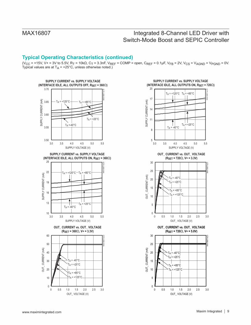
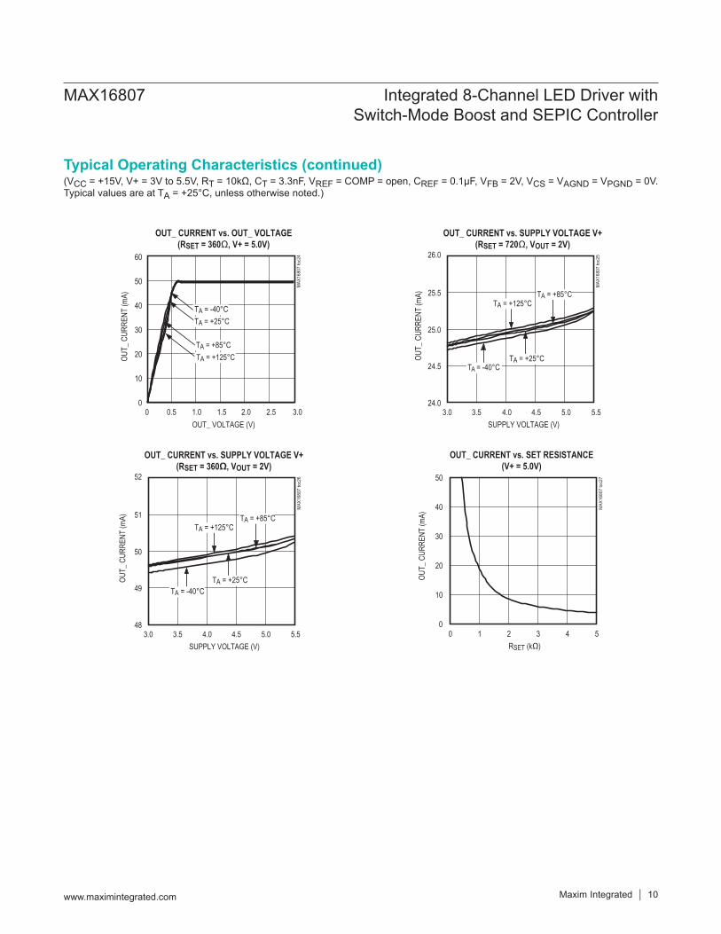
Typical Operating Characteristics
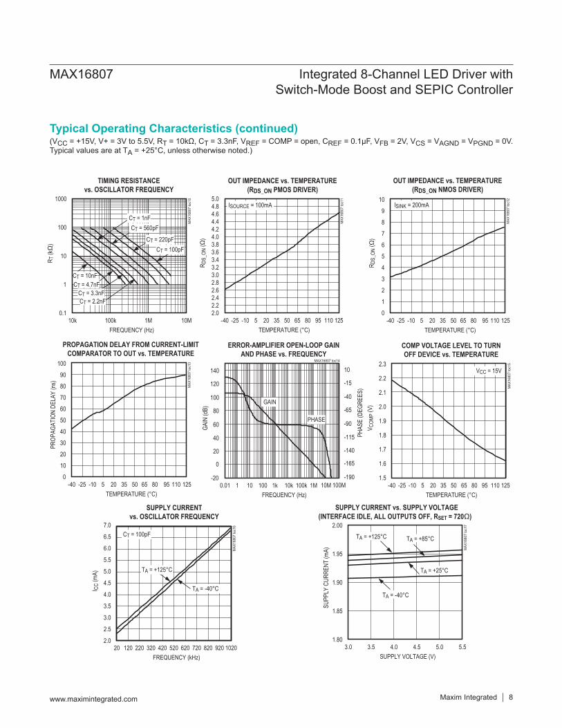
(VCC = +15V, V+ = 3V to 5.5V, RT = 10kΩ, CT = 3.3nF, VREF = COMP = open, CREF = 0.1μF, VFB = 2V, VCS = VAGND = VPGND = 0V. Typical values are at TA = +25°C, unless otherwise noted.)
TIMING RESISTANCEvs. OSCILLATOR FREQUENCY
MAX
1680
7 to
c10
FREQUENCY (Hz)
R T (k
Ω)
1M100k
1
10
100
1000
0.110M10k
CT = 1nFCT = 560pF
CT = 220pFCT = 100pF
CT = 10nFCT = 4.7nF
CT = 3.3nFCT = 2.2nF
OUT IMPEDANCE vs. TEMPERATURE(RDS_ON PMOS DRIVER)
MAX
1680
7 to
c11
TEMPERATURE (°C)
R DS_
ON (Ω
)
1109565 80-10 5 20 35 50-25
2.22.42.62.83.03.23.43.63.84.04.24.44.64.85.0
2.052104-
ISOURCE = 100mA
0
2
1
5
4
3
6
7
9
8
10
OUT IMPEDANCE vs. TEMPERATURE(RDS_ON NMOS DRIVER)
MAX
1680
7 to
c12
R DS_
ON (Ω
)
-40 -10 5 20-25 35 50 9580 11065 125TEMPERATURE (°C)
ISINK = 200mA
0
20
10
50
40
30
60
70
90
80
100
PROPAGATION DELAY FROM CURRENT-LIMITCOMPARATOR TO OUT vs. TEMPERATURE
MAX
1680
7 to
c13
PROP
AGAT
ION
DELA
Y (n
s)
-40 -10 5 20-25 35 50 9580 11065 125TEMPERATURE (°C)
ERROR-AMPLIFIER OPEN-LOOP GAINAND PHASE vs. FREQUENCY
MAX16807 toc14
FREQUENCY (Hz)
GAIN
(dB)
1M100k1k 10k10 1001
0
20
40
60
80
100
120
140
-200.01 100M10M
-165
-140
-115
-90
-65
-40
-15
10
-190
PHASE
GAIN
PHAS
E (D
EGRE
ES)
1.5
1.6
2.2
1.8
1.7
1.9
2.0
2.1
2.3
-40 -25 -10 5 20 35 50 65 80 95 110 125
COMP VOLTAGE LEVEL TO TURNOFF DEVICE vs. TEMPERATURE
MAX
1680
7 to
c15
TEMPERATURE (°C)
V COM
P (V
)VCC = 15V
2.0
3.0
2.5
4.0
3.5
5.0
4.5
5.5
6.5
6.0
7.0
20 120 220 320 420 520 620 720 820 920 1020
SUPPLY CURRENTvs. OSCILLATOR FREQUENCY
MAX
1680
7 to
c16
FREQUENCY (kHz)
I CC
(mA) TA = +125°C
CT = 100pF
TA = -40°C
SUPPLY CURRENT vs. SUPPLY VOLTAGE(INTERFACE IDLE, ALL OUTPUTS OFF, RSET = 720Ω)
MAX
1680
7 to
c17
SUPPLY VOLTAGE (V)
SUPP
LY C
URRE
NT (m
A)
5.04.54.03.5
1.85
1.90
1.95
2.00
1.805.53.0
TA = +125°C TA = +85°C
TA = -40°C
TA = +25°C
Maxim Integrated 8www.maximintegrated.com
MAX16807 Integrated 8-Channel LED Driver withSwitch-Mode Boost and SEPIC Controller
Typical Operating Characteristics (continued)
(VCC = +15V, V+ = 3V to 5.5V, RT = 10kΩ, CT = 3.3nF, VREF = COMP = open, CREF = 0.1μF, VFB = 2V, VCS = VAGND = VPGND = 0V. Typical values are at TA = +25°C, unless otherwise noted.)
SUPPLY CURRENT vs. SUPPLY VOLTAGE(INTERFACE IDLE, ALL OUTPUTS OFF, RSET = 360Ω)
MAX
1680
7 to
c18
SUPPLY VOLTAGE (V)
SUPP
LY C
URRE
NT (m
A)
5.04.54.03.5
3.55
3.60
3.65
3.70
3.505.50.3
TA = +125°C TA = +85°C
TA =-40°C
TA = +25°C
5
8
11
14
17
20
SUPPLY CURRENT vs. SUPPLY VOLTAGE(INTERFACE IDLE, ALL OUTPUTS ON, RSET = 720Ω)
MAX
1680
7 to
c19
SUPPLY VOLTAGE (V)SU
PPLY
CUR
RENT
(mA)
TA = +125°C
TA = -40°CTA = +25°C
TA = +85°C
3.0 3.5 4.0 4.5 5.0 5.5
10
13
16
19
22
25
3.0 3.5 4.0 4.5 5.0 5.5
SUPPLY CURRENT vs. SUPPLY VOLTAGE(INTERFACE IDLE, ALL OUTPUTS ON, RSET = 360Ω)
MAX
1680
7 to
c20
SUPPLY VOLTAGE (V)
SUPP
LY C
URRE
NT (m
A) TA = +125°C
TA = -40°CTA = +25°C
TA = +85°C
0
10
5
20
15
25
30
OUT_ CURRENT vs. OUT_ VOLTAGE(RSET = 720Ω, V+ = 3.3V)
MAX
1680
7 to
c21
OUT_ VOLTAGE (V)
OUT_
CUR
RENT
(mA)
0 1.0 1.50.5 2.0 2.5 3.0
TA = +25°CTA = -40°C
TA = +85°CTA = +125°C
0
20
10
40
30
50
60
OUT_ CURRENT vs. OUT_ VOLTAGE(RSET = 360Ω, V+ = 3.3V)
MAX
1680
7 to
c22
OUT_ VOLTAGE (V)
OUT_
CUR
RENT
(mA)
0 0.5 1.0 1.5 2.0 2.5 3.0
TA = +85°C
TA = +25°C
TA = +125°C
TA = -40°C
0
10
5
20
15
25
30
OUT_ CURRENT vs. OUT_ VOLTAGE(RSET = 720Ω, V+ = 5.0V)
MAX
1680
7 to
c23
OUT_ VOLTAGE (V)
OUT_
CUR
RENT
(mA)
0 1.0 1.50.5 2.0 2.5 3.0
TA = +25°CTA = -40°C
TA = +85°CTA = +125°C
Maxim Integrated 9www.maximintegrated.com
MAX16807 Integrated 8-Channel LED Driver withSwitch-Mode Boost and SEPIC Controller
Typical Operating Characteristics (continued)
(VCC = +15V, V+ = 3V to 5.5V, RT = 10kΩ, CT = 3.3nF, VREF = COMP = open, CREF = 0.1μF, VFB = 2V, VCS = VAGND = VPGND = 0V. Typical values are at TA = +25°C, unless otherwise noted.)
0
20
10
40
30
50
60
OUT_ CURRENT vs. OUT_ VOLTAGE(RSET = 360Ω, V+ = 5.0V)
MAX
1680
7 to
c24
OUT_ VOLTAGE (V)
OUT_
CUR
RENT
(mA)
0 1.0 1.50.5 2.0 2.5 3.0
TA = +25°CTA = -40°C
TA = +85°CTA = +125°C
24.0
24.5
25.0
25.5
26.0
3.0 4.03.5 4.5 5.0 5.5
OUT_ CURRENT vs. SUPPLY VOLTAGE V+(RSET = 720Ω, VOUT = 2V)
MAX
1680
7 to
c25
SUPPLY VOLTAGE (V)OU
T_ C
URRE
NT (m
A)
TA = +125°C
TA = -40°CTA = +25°C
TA = +85°C
48
49
50
51
52
3.0 4.03.5 4.5 5.0 5.5
OUT_ CURRENT vs. SUPPLY VOLTAGE V+(RSET = 360Ω, VOUT = 2V)
MAX
1680
7 to
c26
SUPPLY VOLTAGE (V)
OUT_
CUR
RENT
(mA)
TA = +125°C
TA = -40°CTA = +25°C
TA = +85°C
OUT_ CURRENT vs. SET RESISTANCE(V+ = 5.0V)
MAX
1680
7 to
c27
RSET (kΩ)
OUT_
CUR
RENT
(mA)
4321
10
20
30
40
50
050
Maxim Integrated 10www.maximintegrated.com
MAX16807 Integrated 8-Channel LED Driver withSwitch-Mode Boost and SEPIC Controller
Typical Operating Characteristics (continued)
Detailed DescriptionThe MAX16807 LED driver includes an internal switch-mode controller that can be used as boost or buck-boost (SEPIC) converters to generate the voltage necessary to drive the multiple strings of LEDs. This device incorporates an integrated low-side driver, programmable oscillator (20kHz to 1MHz), error amplifier, low-voltage (300mV) current sense for higher efficiency, and a 5V reference to power up external circuitry (see Figures 1a and 1b).The MAX16807 LED driver includes a 4-wire serial inter-face and a current-mode PWM controller to generate the necessary voltage for driving eight open-drain, constant-current-sinking output ports. The driver uses current-
sensing feedback circuitry (not simple current mirrors) to ensure very small current variations over the full allowed range of output voltage (see the Typical Operating Characteristics). The 4-wire serial interface comprises an 8-bit shift register and an 8-bit transparent latch. The shift register is written through a clock input (CLK) and a data input (DIN), and the data propagates to a data output (DOUT). The data output allows multiple drivers to be cascaded and operated together. The contents of the 8-bit shift register are loaded into the transparent latch through a latch-enable input (LE). The latch is transpar-ent to the shift-register outputs when high and latches the current state on the falling edge of LE. Each driver output is an open-drain, constant-current sink that should be connected to the cathode of a string of LEDs con-
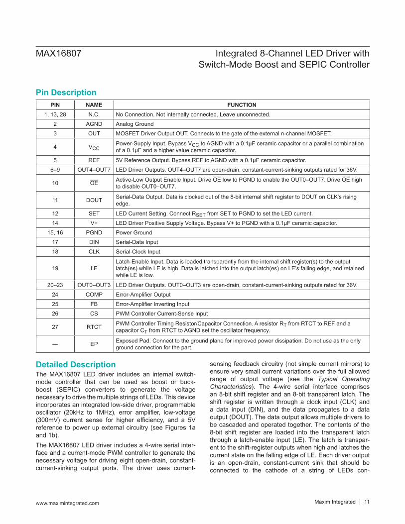
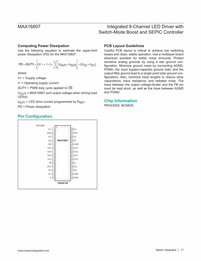
PIN NAME FUNCTION1, 13, 28 N.C. No Connection. Not internally connected. Leave unconnected.
2 AGND Analog Ground
3 OUT MOSFET Driver Output OUT. Connects to the gate of the external n-channel MOSFET.
4 VCCPower-Supply Input. Bypass VCC to AGND with a 0.1µF ceramic capacitor or a parallel combination of a 0.1µF and a higher value ceramic capacitor.
5 REF 5V Reference Output. Bypass REF to AGND with a 0.1µF ceramic capacitor.
6–9 OUT4–OUT7 LED Driver Outputs. OUT4–OUT7 are open-drain, constant-current-sinking outputs rated for 36V.
10 OE Active-Low Output Enable Input. Drive OE low to PGND to enable the OUT0–OUT7. Drive OE high to disable OUT0–OUT7.
11 DOUT Serial-Data Output. Data is clocked out of the 8-bit internal shift register to DOUT on CLK’s rising edge.
12 SET LED Current Setting. Connect RSET from SET to PGND to set the LED current.
14 V+ LED Driver Positive Supply Voltage. Bypass V+ to PGND with a 0.1µF ceramic capacitor.
15, 16 PGND Power Ground
17 DIN Serial-Data Input
18 CLK Serial-Clock Input
19 LELatch-Enable Input. Data is loaded transparently from the internal shift register(s) to the output latch(es) while LE is high. Data is latched into the output latch(es) on LE’s falling edge, and retained while LE is low.
20–23 OUT0–OUT3 LED Driver Outputs. OUT0–OUT3 are open-drain, constant-current-sinking outputs rated for 36V.
24 COMP Error-Amplifier Output
25 FB Error-Amplifier Inverting Input
26 CS PWM Controller Current-Sense Input
27 RTCT PWM Controller Timing Resistor/Capacitor Connection. A resistor RT from RTCT to REF and a capacitor CT from RTCT to AGND set the oscillator frequency.
— EP Exposed Pad. Connect to the ground plane for improved power dissipation. Do not use as the only ground connection for the part.
MAX16807 Integrated 8-Channel LED Driver withSwitch-Mode Boost and SEPIC Controller
www.maximintegrated.com Maxim Integrated 11
Pin Description

nected in series. The constant-current capability is up to 55mA per output, set for all eight outputs by an external resistor (RSET). The device can operate in stand-alone mode (see the Typical Operating Circuits.)
The number of channels can be expanded by using the MAX6970 and MAX6971 family in conjunction with the MAX16807.
Figure 1a. Internal Block Diagram (MAX16807)
2R
R
26.5V
EN_REFBGSNS
300mV
UVLO
ILIM
VEA
CPWM
VOLTAGE-DIVIDER
VDD
THERMALSHUTDOWN
VOLTAGEDIVIDER
OSC
CLK
PREREG5V
REG_OK
5V REG
REFERENCE2.5V
DELAY
SR
Q
Q
VCC
V+
CURRENTREFERENCE
POWER-ONRESET
THERMALSHUTDOWN
D0 D1 D2 D3 D4 D5 D6 D7
D0 D1 D2 D3 D4 D5 D6 D7
D0 D1 D2 D3 D4 D5 D6 D7
CONSTANT-CURRENT SINK
OUTPUT LATCHES
SERIAL-TO-PARALLEL SHIFT REGISTER
AGND
CS
VCC
REF
OUT
RTCT
DOUT
V+
SET
FB
COMP
CLK
DIN
LE
OE
OUT0
OUT1
OUT2
OUT3
OUT4
OUT5
OUT6
OUT7
PGND
MAX16807
MAX16807 Integrated 8-Channel LED Driver withSwitch-Mode Boost and SEPIC Controller
www.maximintegrated.com Maxim Integrated 12
Switch-Mode ControllerCurrent-Mode Control LoopThe advantages of current-mode control over voltage-mode control are twofold. First, there is the feed-forward characteristic brought on by the controller’s ability to adjust for variations in the input voltage on a cycle-by-cycle basis. Second, the stability requirements of the current-mode controller are reduced to that of a single-pole system, unlike the double pole in the voltage-mode control scheme. The MAX16807 uses a current-mode control loop where the output of the error amplifier is compared to the current-sense voltage (VCS). When the current-sense signal is lower than the inverting input of the CPWM comparator, the output of the comparator is low and the switch is turned on at each clock pulse. When the current-sense signal is higher than the inverting input of the CPWM comparator, the output is high and the switch is turned off.
Undervoltage Lockout (UVLO)The turn-on supply voltage for the MAX16807 is 8.4V (typ). Once VCC reaches 8.4V, the reference powers up. There is 0.8V of hysteresis from the turn-on voltage to the UVLO threshold. Once VCC reaches 8.4V, the MAX16807 operates with VCC down to 7.6V (typ). Once VCC goes below 7.6V, the device is in UVLO. When in UVLO, the quiescent supply current into VCC falls back to 32μA (typ), and OUT and REF are pulled low.
MOSFET DriverOUT drives an external n-channel MOSFET and swings from AGND to VCC. Ensure that VCC remains below the
absolute maximum VGS rating of the external MOSFET. OUT is a push-pull output with the on-resistance of the pMOS (typically 3.5Ω) and the on-resistance of the nMOS (typically 4.5Ω). The driver can source 2A and sink 1A (typ). This allows for the MAX16807 to quickly turn on and off high gate-charge MOSFETs. Bypass VCC with one or more 0.1μF ceramic capacitors to AGND, placed close to the VCC pin. The average current sourced to drive the external MOSFET depends on the total gate charge (QG) and operating frequency of the converter. The power dissipation in the device is a function of the average out-put drive current (IDRIVE). Use the following equation to calculate the power dissipation in the device due to IDRIVE:
IDRIVE = (QG x fSW)PD = (IDRIVE + ICC) x VCC
where ICC is the operating supply current. See the Typical Operating Characteristics for the operating supply current at a given frequency.
Error AmplifierThe MAX16807 includes an internal error amplifier. The inverting input is at FB and the noninverting input is internally connected to a 2.5V reference. Set the output voltage using a resistive divider between the output of the converter (VOUT, FB, and AGND). Use the following formula to set the output voltage:
OUT FBR1V 1 VR2
= + ×
where VFB = 2.5V.
OscillatorThe oscillator frequency is programmable using an exter-nal capacitor and a resistor at RTCT (see RT and CT in the Typical Operating Circuits). RT is connected from RTCT to the 5V reference (REF), and CT is connected from RTCT to AGND. REF charges CT through RT until its volt-age reaches 2.8V. CT then discharges through an 8.3mA internal current sink until CT’s voltage reaches 1.1V, at which time CT is allowed to charge through RT again. The oscillator’s period is the sum of the charge and discharge times of CT. Calculate the charge time as follows:
tC = 0.57 x RT x CTwhere tC is in seconds, RT in ohms (Ω), and CT in Farads (F).The discharge time is then:
tD = (RT x CT x 1000)/[(4.88 x RT) - (1.8 x 1000)]where tD is in seconds, RT in ohms (Ω), and CT in Farads (F).
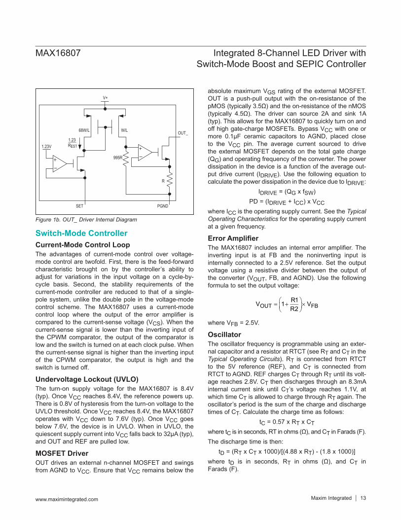
Figure 1b. OUT_ Driver Internal Diagram
V+
W/L OUT_68W/L
995R
REST1.23
R
1.23V
PGNDSET
MAX16807 Integrated 8-Channel LED Driver withSwitch-Mode Boost and SEPIC Controller
www.maximintegrated.com Maxim Integrated 13
The oscillator frequency is then:
OSCC D(t t )
Reference Output (REF)REF is a 5V reference output that can source 20mA. Bypass REF to AGND with a 0.1μF capacitor.
Current LimitThe MAX16807 includes a fast current-limit comparator to terminate the on-cycle during an overload or a fault condition. The current-sense resistor (RCS) connected between the source of the external MOSFET and AGND, sets the current limit. The CS input has a voltage trip level (VCS) of 0.3V. Use the following equation to calculate RCS:
CSCS
P P
VRI −
=
IP-P is the peak current that flows through the MOSFET. When the voltage produced by this current (through the current-sense resistor) exceeds the current-limit compar-ator threshold, the MOSFET driver (OUT) turns the switch off within 60ns. In most cases, a small RC filter is required to filter out the leading-edge spike on the sense wave-form. Set the time constant of the RC filter at 50ns.
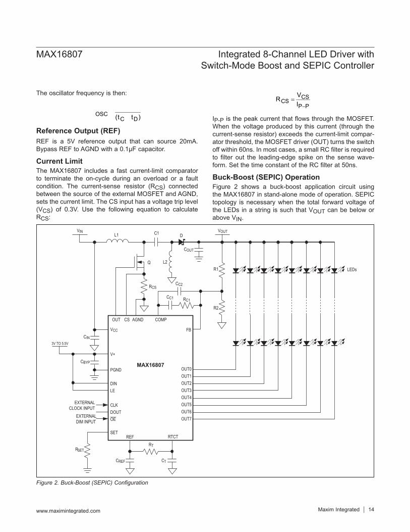
Buck-Boost (SEPIC) OperationFigure 2 shows a buck-boost application circuit using the MAX16807 in stand-alone mode of operation. SEPIC topology is necessary when the total forward voltage of the LEDs in a string is such that VOUT can be below or above VIN.
Figure 2. Buck-Boost (SEPIC) Configuration
MAX16807OUT0
FB
OUT1OUT2OUT3OUT4OUT5OUT6OUT7EXTERNAL
DIM INPUT
EXTERNALCLOCK INPUT
SET
LEDIN
PGND
VCC
V+
OEDOUTCLK
REF RTCT
CREF
CBYP
RSET
RCS
C1 D
CC2
CC1
OUT CS AGND COMP
RC1
R2
R1
CIN
RT
CT
3V TO 5.5V
VIN VOUT
QLEDs
L1
L2
COUT
MAX16807 Integrated 8-Channel LED Driver withSwitch-Mode Boost and SEPIC Controller
www.maximintegrated.com Maxim Integrated 14
LED Driver4-Wire InterfaceThe MAX16807 also operates in stand-alone mode (see the Typical Operating Circuits). For use with a microcon-troller, the MAX16807 features a 4-wire serial interface using DIN, CLK, LE, OE inputs and DOUT as a data out-put. This interface is used to write the LED channels’ data to the MAX16807. The serial-interface data word length is 8 bits (D0–D7). See Figure 3.The functions of the five interface pins are as follows: DIN is the serial-data input, and must be stable when it is sampled on the rising edge of CLK. Data is shifted in MSB first. This means that data bit D7 is clocked in first, followed by seven more data bits, finishing with the LSB (D0).CLK is the serial-clock input that shifts data at DIN into the MAX16807’s 8-bit shift register on its rising edge.LE is the latch-enable input of the MAX16807 that trans-fers data from the 8-bit shift register to its 8-bit output latch (transparent latch). The data is latched on the falling edge of LE (Figure 4). The fourth input (OE) provides output-enable control of the output drivers. When OE is driven high, the outputs (OUT0–OUT7) are forced to high imped-ance without altering the contents of the output latches. Driving OE low enables the outputs to follow the state of the output latches. OE is independent of the operation of the serial interface operation. Data can be shifted into the serial-interface shift register and latched, regardless of the state of OE. DOUT is the serial-data output that
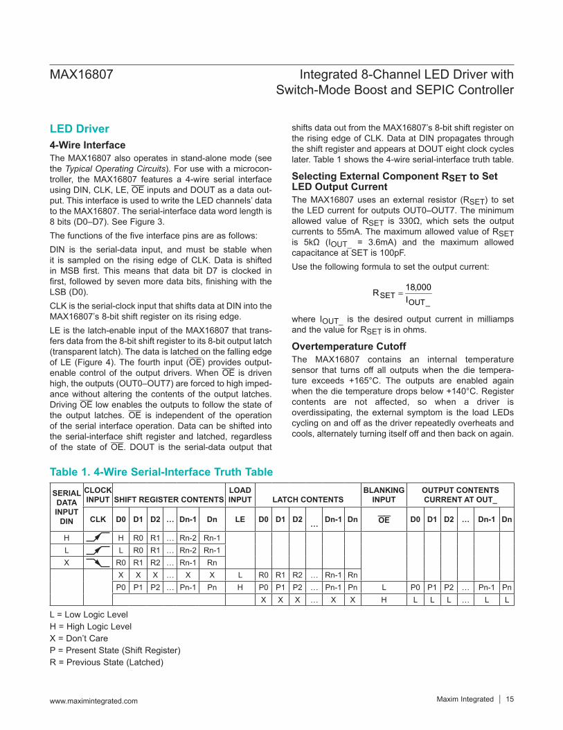
shifts data out from the MAX16807’s 8-bit shift register on the rising edge of CLK. Data at DIN propagates through the shift register and appears at DOUT eight clock cycles later. Table 1 shows the 4-wire serial-interface truth table.
Selecting External Component RSET to Set LED Output CurrentThe MAX16807 uses an external resistor (RSET) to set the LED current for outputs OUT0–OUT7. The minimum allowed value of RSET is 330Ω, which sets the output currents to 55mA. The maximum allowed value of RSET is 5kΩ (IOUT_ = 3.6mA) and the maximum allowed capacitance at SET is 100pF.Use the following formula to set the output current:
SETOUT_
18,000RI
=
where IOUT_ is the desired output current in milliamps and the value for RSET is in ohms.
Overtemperature CutoffThe MAX16807 contains an internal temperature sensor that turns off all outputs when the die tempera-ture exceeds +165°C. The outputs are enabled again when the die temperature drops below +140°C. Register contents are not affected, so when a driver is overdissipating, the external symptom is the load LEDs cycling on and off as the driver repeatedly overheats and cools, alternately turning itself off and then back on again.
L = Low Logic LevelH = High Logic LevelX = Don’t CareP = Present State (Shift Register)R = Previous State (Latched)
Table 1. 4-Wire Serial-Interface Truth Table
SERIAL DATA INPUT
DIN
CLOCK INPUT SHIFT REGISTER CONTENTS
LOAD INPUT LATCH CONTENTS
BLANKING INPUT
OUTPUT CONTENTS CURRENT AT OUT_
CLK D0 D1 D2 … Dn-1 Dn LE D0 D1 D2 … Dn-1 Dn OE D0 D1 D2 … Dn-1 Dn
H H R0 R1 … Rn-2 Rn-1L L R0 R1 … Rn-2 Rn-1X R0 R1 R2 … Rn-1 Rn
X X X … X X L R0 R1 R2 … Rn-1 RnP0 P1 P2 … Pn-1 Pn H P0 P1 P2 … Pn-1 Pn L P0 P1 P2 … Pn-1 Pn
X X X … X X H L L L … L L
MAX16807 Integrated 8-Channel LED Driver withSwitch-Mode Boost and SEPIC Controller
www.maximintegrated.com Maxim Integrated 15

Stand-Alone OperationIn stand-alone operation, the MAX16807 does not use the 4-wire interface (see the Typical Operating Circuits). Connecting DIN and LE to V+ provides at least eight external clock pulses to CLK to enable the RSET outputs. This startup pulse sequence can be provided either using an external clock or the PWM signal. The external clock can also be generated using the signal at RTCT and an external comparator.
LED DimmingPWM DimmingAll the output channels can be dimmed simultaneously by applying a PWM signal (50Hz to 30kHz) to OE. This allows for a wide range of dimming up to a 5000:1 ratio. Each channel can be independently turned on and off using a 4-wire serial interface. The dimming is proportional to the PWM duty cycle.
LED Current-Amplitude AdjustmentUsing an analog or digital potentiometer as RSET allows for LED current-amplitude adjustment and linear dimming.
Figure 3. 4-Wire Serial-Interface Timing Diagram
Figure 4. LE and CLK to OUT_ Timing
tDStDH
tCLtCP
tDO
tOEW
tOEF
tf tr
tOER
tLS
tLWtCH
D0
D7
D7
LE
CLK
DIN
DOUT
OE
OUT_80%
20%
LE
OUT_
LE
OUT_
CLK
OUT_
CLK
OUT_
tCRR
tCRF
tLRR
tLRF
MAX16807 Integrated 8-Channel LED Driver withSwitch-Mode Boost and SEPIC Controller
www.maximintegrated.com Maxim Integrated 16
Computing Power DissipationUse the following equation to estimate the upper-limit power dissipation (PD) for the MAX16807:
( ) ( )i 7
OUTi OUTi CC CCi 0
PD DUTY V I V I V I=
=
= × + × + + × + × ∑
where:V+ = Supply voltageI+ = Operating supply currentDUTY = PWM duty cycle applied to OEVOUTi = MAX16807 port output voltage when driving load LED(s)IOUTi = LED drive current programmed by RSETPD = Power dissipation
PCB Layout GuidelinesCareful PCB layout is critical to achieve low switching losses and clean, stable operation. Use a multilayer board whenever possible for better noise immunity. Protect sensitive analog grounds by using a star ground con-figuration. Minimize ground noise by connecting AGND, PGND, the input bypass-capacitor ground lead, and the output-filter ground lead to a single point (star ground con-figuration). Also, minimize trace lengths to reduce stray capacitance, trace resistance, and radiated noise. The trace between the output voltage-divider and the FB pin must be kept short, as well as the trace between AGND and PGND.
28
27
26
25
24
23
22
1
2
3
4
5
6
7
N.C.
RTCT
CS
FBVCC
OUT
AGND
N.C.
TOP VIEW
MAX16807COMP
OUT3
OUT2OUT5
OUT4
21 OUT18
OUT09
OUT6
20OUT7
19 LE10OE
18 CKL11DOUT
17 DIN12SET
16 PGND13N.C.
15 PGND14V+
REF
TSSOP-EP
+
MAX16807 Integrated 8-Channel LED Driver withSwitch-Mode Boost and SEPIC Controller
www.maximintegrated.com Maxim Integrated 17
Pin Configuration
Chip InformationPROCESS: BiCMOS
PACKAGE TYPE PACKAGE CODE DOCUMENT NO.28 TSSOP U28ME+1 21-0108
MAX16807OUT0
FB
OUT1OUT2OUT3OUT4OUT5OUT6OUT7
SET
PGND
VCC
V+
OELEDOUTDINCLKSCLK
MOSIMISOµC
LOADENABLE
REF RTCT
CREF
RSET
RCSCC2
CC1
OUT CS AGND COMP
RC1
R2
R1
COUT
RT
CT
3V TO 5.5V
VIN VOUT
Q
L D
LEDs
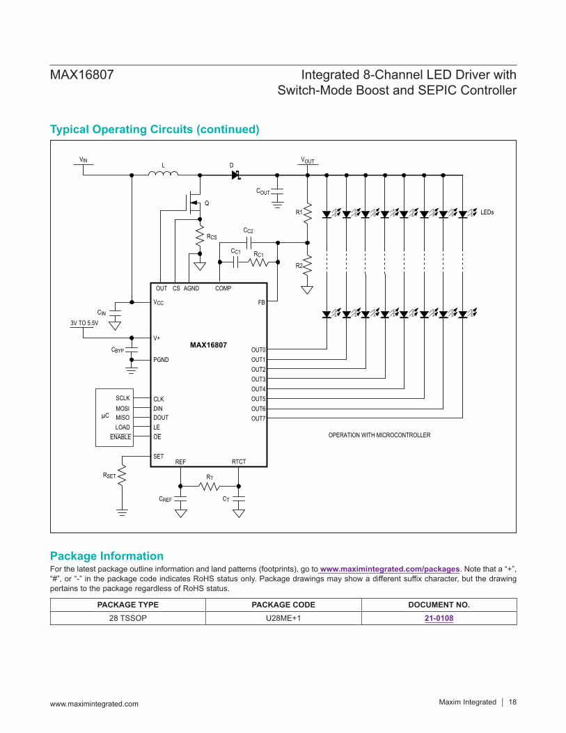
OPERATION WITH MICROCONTROLLER
CIN
CBYP
MAX16807 Integrated 8-Channel LED Driver withSwitch-Mode Boost and SEPIC Controller
www.maximintegrated.com Maxim Integrated 18
Package InformationFor the latest package outline information and land patterns (footprints), go to www.maximintegrated.com/packages. Note that a “+”, “#”, or “-” in the package code indicates RoHS status only. Package drawings may show a different suffix character, but the drawing pertains to the package regardless of RoHS status.
Typical Operating Circuits (continued)
REVISION NUMBER
REVISION DATE DESCRIPTION PAGES
CHANGED
0 10/06 Initial release —
1 4/07 Release of the MAX16808 12 8/09 Removal of the MAX16808 from the data sheet. 1–21
3 11/14 No /V OPN in Ordering Information, removed automotive reference in Applications section 1
Maxim Integrated cannot assume responsibility for use of any circuitry other than circuitry entirely embodied in a Maxim Integrated product. No circuit patent licenses are implied. Maxim Integrated reserves the right to change the circuitry and specifications without notice at any time. The parametric values (min and max limits) shown in the Electrical Characteristics table are guaranteed. Other parametric values quoted in this data sheet are provided for guidance.
Maxim Integrated and the Maxim Integrated logo are trademarks of Maxim Integrated Products, Inc. © 2014 Maxim Integrated Products, Inc. 19
MAX16807 Integrated 8-Channel LED Driver withSwitch-Mode Boost and SEPIC Controller
Revision History
For pricing, delivery, and ordering information, please contact Maxim Direct at 1-888-629-4642, or visit Maxim Integrated’s website at www.maximintegrated.com.


![Semantic construction with s-graph grammars€¦ · Example: the boy wants to sleep 25 term h s (t) • the boy • wants to sleep f subj(∙) ‖ f vcomp(∙) ∙[subj] ‖ G 1 ∙[vcomp]](https://static.fdocuments.in/doc/165x107/60618ea8525600319e3ccad1/semantic-construction-with-s-graph-grammars-example-the-boy-wants-to-sleep-25-term.jpg)